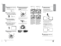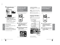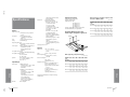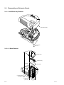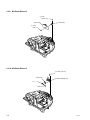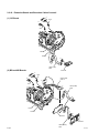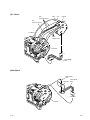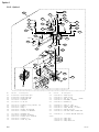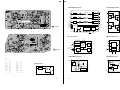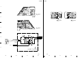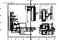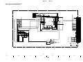
1
SERVICE MANUAL MODEL .............. VPL-HS1 VPL-HS1FP DEST. ......... MODEL .............. DEST. ......... WORLD RM-PJHS1 WORLD WORLD SU-HS1 WORLD IFU-HS1 WORLD LCD VIDEO PROJECTOR ! WARNING This manual is intended for qualified service personnel only. To reduce the risk of electric shock, fire or injury, do not perform any servicing other than that contained in the operating instructions unless you are qualified to do so. Refer all servicing to qualified service personnel. ! WARNUNG Die Anleitung ist nur für qualifiziertes Fachpersonal bestimmt. Alle Wartungsarbeiten dürfen nur von qualifiziertem Fachpersonal ausgeführt werden. Um die Gefahr eines elektrischen Schlages, Feuergefahr und Verletzungen zu vermeiden, sind bei Wartungsarbeiten strikt die Angaben in der Anleitung zu befolgen. Andere als die angegeben Wartungsarbeiten dürfen nur von Personen ausgeführt werden, die eine spezielle Befähigung dazu besitzen. ! AVERTISSEMENT Ce manual est destiné uniquement aux personnes compétentes en charge de l’entretien. Afin de réduire les risques de décharge électrique, d’incendie ou de blessure n’effectuer que les réparations indiquées dans le mode d’emploi à moins d’être qualifié pour en effectuer d’autres. Pour toute réparation faire appel à une personne compétente uniquement. WARNING!! ATTENTION!! AN INSULATED TRANSFORMER SHOULD BE USED DURING ANY SERVICE TO AVOID POSSIBLE SHOCK HAZARD, BECAUSE OF LIVE CHASSIS. THE CHASSIS OF THIS RECEIVER IS DIRECTLY CONNECTED TO THE AC POWER LINE. AFIN D’ÉVITER TOUT RISQUE D’ÉLECTROCUTION PROVENANT D’UN CHÂSSIS SOUS TENSION, UN TRANSFORMATEUR D’ISOLEMENT DOIT ETRE UTILISÉ LORS DE TOUT DÉPANNAGE. LE CHÂSSIS DE CE RÉCEPTEUR EST DIRECTEMENT RACCORDÉ Á L’ALIMENTATION SECTEUR. SAFETY-RELATED COMPONENT WARNING !! ATTENTION AUX COMPOSANTS RELATIFS Á LA SÉCURITÉ!! COMPONENTS IDENTIFIED BY A ! MARK ON THE SCHEMATIC DIAGRAMS, EXPLODED VIEWS AND IN THE PARTS LIST ARE CRITICAL TO SAFE OPERATION. REPLACE THESE COMPONENTS WITH SONY PARTS WHOSE PART NUMBERS APPEAR AS SHOWN IN THIS MANUAL OR IN SUPPLEMENTS PUBLISHED BY SONY. LES COMPOSANTS IDENTIFIÉS PAR UNE MAPQUE ! SUR LES SCHÉMAS DE PRINCIPE, LES VUES EXPLOSÉES ET LES LISTES DE PIECES SONT D’UNE IMPORTANCE CRITIQUE POUR LA SÉCURITÉ DU FONCTIONNEMENT. NE LES REMPLACER QUE PAR DES COMPOSANTS SONY DONT LE NUMÉRO DE PIÈCE EST INDIQUÉ DANS LE PRÉSENT MANUEL OU DANS DES SUPPLÉMENTS PUBLIÉS PAR SONY. For the customers in the Netherlands Voor de klanten in Nederland •Gooi de batterij niet weg, maar lever hem in als KCA. NL Table of Contents 1. Operating Instructions 1-1. 1-2. 1-3. VPL-HS1 ..................................................................................................... 1-1 SU-HS1 ..................................................................................................... 1-25 IFU-HS1 .................................................................................................... 1-27 2. Service Informations 2-1. 2-2. 2-3. Board Layout ............................................................................................... 2-1 Disassembly and Extension Boards ............................................................ 2-2 2-2-1. Hood Block Assy Removal ........................................................ 2-2 2-2-2. H Board Removal ....................................................................... 2-2 2-2-3. C Board Removal ....................................................................... 2-3 2-2-4. MS Board Removal .................................................................... 2-3 2-2-5. BB and NF Boards Removal ...................................................... 2-4 2-2-6. BC Board Removal .................................................................... 2-4 2-2-7. Optics block assy Removal ........................................................ 2-5 2-2-8. Q Board Removal ....................................................................... 2-5 2-2-9. BA Board Removal .................................................................... 2-6 2-2-10. NR Board Removal .................................................................... 2-6 2-2-11. F Board Removal ....................................................................... 2-7 2-2-12. Hi-voltage block and G Board Removal .................................... 2-7 2-2-13. Projection Lens Removal ........................................................... 2-8 2-2-14. Prism Block Assy and In-polarizer Removal ............................. 2-8 2-2-15. Extension Boards and Extension Cables .................................... 2-9 2-2-16. Extension Boards and Extension Cables Connection .............. 2-10 (1)BC Board ............................................................................. 2-10 (2)BB and MS Boards .............................................................. 2-10 (3)C Board ................................................................................ 2-11 (4)BA Board ............................................................................. 2-11 (5)Q Board ............................................................................... 2-12 Power cord ................................................................................................ 2-12 3. Electrical Adjustments 3-1. 3-2. 3-3. 3-4. VPL-HS1 Preparations ................................................................................................. 3-1 3-1-1. Equipment Required ................................................................... 3-1 3-1-2. Optical Unit Adjustment ............................................................ 3-1 3-1-3. Factory Mode Setting ................................................................. 3-1 V-COM Adjustment .................................................................................... 3-1 Adjustment Item Initialize Data .................................................................. 3-2 Service Knowhow ....................................................................................... 3-6 1 3-5. 3-6. 3-4-1. After Replacing the Prism Block ............................................... 3-6 3-4-2. After Replacing the Board ......................................................... 3-6 White Balance Adjustment on Servicing .................................................... 3-7 3-5-1. Signal Level Adjustment ............................................................ 3-7 3-5-2. White Balance Adjustment ........................................................ 3-7 Memory ....................................................................................................... 3-9 4. Semiconductors IC ................................................................................................................. 4-1 Transistor ..................................................................................................... 4-3 Diode ........................................................................................................... 4-4 5. Spare Parts 5-1. 5-2. 5-3. 5-4. 5-5. 5-6. Notes on Repair Parts .................................................................................. 5-1 Exploded Views .......................................................................................... 5-2 5-2-1. Cover .......................................................................................... 5-2 5-2-2. Chassis 1 ..................................................................................... 5-3 5-2-3. Chassis 2 ..................................................................................... 5-4 5-2-4. Stand ........................................................................................... 5-5 5-2-5. Optics 1 ...................................................................................... 5-6 5-2-6. Optics 2 ...................................................................................... 5-7 5-2-7. Stand(SU-HS1) .......................................................................... 5-8 Electrical Parts List ..................................................................................... 5-9 Packing Materials ...................................................................................... 5-31 IFU-HS1 .................................................................................................... 5-31 SU-HS1 ..................................................................................................... 5-31 6. Block Diagrams Q Block ....................................................................................................... 6-1 BA Block ..................................................................................................... 6-2 BB Block ..................................................................................................... 6-3 BC and H Blocks ......................................................................................... 6-4 G Block ....................................................................................................... 6-5 MS Block .................................................................................................... 6-6 C Block ........................................................................................................ 6-7 2 VPL-HS1 7. Diagrams 7-1. 7-2. VPL-HS1 Frame Schematic Diagram .......................................................................... 7-1 Schematic Diagrams and Printed Wiring Boards ........................................ 7-3 Schematic Diagrams BA ......................................................................................................... 7-5 BB ......................................................................................................... 7-9 BC ....................................................................................................... 7-14 C ....................................................................................................... 7-17 F ....................................................................................................... 7-24 G ....................................................................................................... 7-26 H ....................................................................................................... 7-28 Q ....................................................................................................... 7-31 NF ....................................................................................................... 7-35 NR ....................................................................................................... 7-35 MS ....................................................................................................... 7-37 Printed Wiring Boards BA ......................................................................................................... 7-4 BB ......................................................................................................... 7-8 BC ....................................................................................................... 7-13 C ....................................................................................................... 7-15 F ....................................................................................................... 7-24 G ....................................................................................................... 7-25 H ....................................................................................................... 7-28 Q ....................................................................................................... 7-29 NF ....................................................................................................... 7-35 NR ....................................................................................................... 7-35 MS ....................................................................................................... 7-36 3 1-1. VPL-HS1 VPL-HS1 4-085-330-11 (1) LCD Video Projector Manual de instrucciones __________________________________ES 1-1 Reprinted from the operating instructions VPL-HS1 © 2001 Sony Corporation ___________________________________GB _________________________________________FR Section 1 Operating Instructions Operating Instructions Mode d’emploi 1-2 WARNING To prevent fire or shock hazard, do not expose the unit to rain or moisture. To avoid electrical shock, do not open the cabinet. Refer servicing to qualified personnel only. This symbol is intended to alert the user to the presence of uninsulated "dangerous voltage" within the product's enclosure that may be of sufficient magnitude to constitute a risk of electric shock to persons. This symbol is intended to alert the user to the presence of important operating and maintenance (servicing) instructions in the literature accompanying the appliance. For the customers in the USA If you have any questions about this product, you may contact: Sony Electronics Inc. Attn: Business Information Center (BIC) 12451 Gateway Boulevard Ft. Myers, Florida 33913 Telephone No.: 800-686-7669 The number below is for FCC related matters only. Declaration of Conformity Trade Name: SONY Model No.: VPL-HS1 Responsible Party: Sony Electronics Inc. Address: 680 Kinderkamack Road, Oradell NJ 07649 U.S.A. Telephone No.: 201-930-6972 This device complies with Part 15 of the FCC Rules. Operation is subject to the following two conditions: (1) This device may not cause harmful interference, and (2) this device must accept any interference received, including interference that may cause undesired operation. VPL-HS1 GB 2 This equipment has been tested and found to comply with the limits for a Class B digital device, pursuant to Part 15 of the FCC Rules. These limits are designed to provide reasonable protection against harmful interference in a residential installation. This equipment generates, uses, and can radiate radio frequency energy and, if not installed and used in accordance with the instructions, may cause harmful interference to radio communications. However, there is no guarantee that interference will not occur in a particular installation. If this equipment does cause harmful interference to radio or television reception, which can be determined by turning the equipment off and on, the user is encouraged to try to correct the interference by one or more of the following measures: - Reorient or relocate the receiving antenna. - Increase the separation between the equipment and receiver. - Connect the equipment into an outlet on a circuit different from that to which the receiver is connected. - Consult the dealer or an experienced radio/TV technician for help. You are cautioned that any changes or modifications not expressly approved in this manual could void your authority to operate this equipment. Table of Contents Preparing for Viewing the Still Picture Stored in a “Memory Stick” .................................23 Inserting a “Memory Stick” ..........................23 Using the MS (“Memory Stick”) Home .......24 Precautions ............................................... 4 Connections and Preparations Voor de klanten in Nederland Bij dit product zijn batterijen geleverd. Wanneer deze leeg zijn, moet u ze niet weggooien maar inleveren als KCA. The socket-outlet should be installed near the equipment and be easily accessible. Viewing Still Images in Sequence — Slide Show ..........................................24 Displaying Index Pictures on the Full Screen ..............................................26 Displaying the Index Menu ...........................27 Unpacking ................................................. 5 Displaying a Full-Screen Picture .............27 Step 1: Installing the Projector .................. 5 Rotating a Still Picture .............................28 Before Setting Up the Projector ..................... 6 Protecting an Important Still Picture ........29 Installing the Projector and a Screen .............. 7 Projecting a Selected Picture When the Power Is Turned On — Startup ...............30 Step 2: Connecting the Projector .............. 8 Connecting with video equipment ................. 8 For the customers in Canada This Class B digital apparatus complies with Canadian ICES-003. Using a “Memory Stick” About a “Memory Stick” ..........................22 Registering a Still Picture as the Startup Picture ......................................................30 Connecting Using the Optional Signal Interface Cables ........................................................ 8 Setting the Startup Picture ............................31 Connecting Using the Optional Interface Unit 9 Deleting a Still Picture .............................32 Step 3: Adjusting the Picture Size and Position ..................................................... 9 Initializing a “Memory Stick” ....................33 Step 4: Selecting the Menu Language .... 12 Projecting Others Troubleshooting .......................................34 Replacing the Lamp ................................38 Projecting the Picture on the Screen ...... 14 Replacing the Air Filter ............................39 Selecting the Picture Viewing Mode ....... 16 Specifications ..........................................40 Location of Controls ................................44 Using the Menus Front ..............................................................44 Operation through the Menus ................. 17 Rear ...............................................................45 Menu Configurations ............................... 18 Remote control ..............................................46 Menu Items ................................................... 19 Index .......................................................47 About the Preset Memory No. ..................... 21 Adjusting Picture Quality of a Signal from the Computer ................................................. 21 3GB Connections and Preparations This section describes how to install the projector and screen, how to connect the equipment from which you want to project the picture, etc. Step 1: Installing the Projector Connections and Preparations VPL-HS1 Precautions Unpacking On safety • Check that the operating voltage of your unit is identical with the voltage of your local power supply. • Should any liquid or solid object fall into the cabinet, unplug the unit and have it checked by qualified personnel before operating it further. • Unplug the unit from the wall outlet if it is not to be used for several days. • To disconnect the cord, pull it out by the plug. Never pull the cord itself. • The wall outlet should be near the unit and easily accessible. • The unit is not disconnected to the AC power source (mains) as long as it is connected to the wall outlet, even if the unit itself has been turned off. • Do not look into the lens while the lamp is on. • Do not place your hand or objects near the ventilation holes. The air coming out is hot. On preventing internal heat build-up You can obtain good picture quality even when you project the picture from the side of the screen (“SIDE SHOT”) (1 page 7). You can enjoy home entertainment with this projector in various situations. Enjoying home theater Check the carton to make sure it contains the following items: Remote control (1), Size AA (R6) batteries (2) Signal interface cable (1) Air filter (for replacement) (1) Enjoying video games on a large screen After you turn off the power with the I / 1 (on/ standby) switch, do not disconnect the unit from the wall outlet while the cooling fan is still running. Lens cap (1) Caution The projector is equipped with ventilation holes (intake) and ventilation holes (exhaust). Do not block or place anything near these holes, or internal heat build-up may occur, causing picture degradation or damage to the projector. On repacking Save the original shipping carton and packing material; they will come in handy if you ever have to ship your unit. For maximum protection, repack your unit as it was originally packed at the factory. GB 1-3 4 Precautions AC power cord (1) Operating Instructions (1) Inserting the batteries into the remote control Insert the batteries E side first as shown in the illustration. Unpacking / Step 1: Installing the Projector 5 GB 1-4 Highly heated and humid c: Maximum projection distance between the screen and the center of the projector’s lens when you use the horizontal distance a, or when you place the projector with the center of the screen and the center of the lens aligned. d: Minimum projection distance between the screen and the center of the lens when you use the horizontal distance b, or when you place the projector with the center of the screen and the center of the lens aligned. Installing the Projector and a Screen The installation distance between the projector and screen varies depending on the size of the screen. 1 Determine the installation position of the projector and screen. Very dusty and extremely smoky Viewing images, recorded by a digital camera and stored in the “Memory Stick,” on a large screen. Do not use the projector under the following conditions. Tilting the unit out of the range of the adjuster setting When projecting from the side (SIDE SHOT) Position the projector with the lens end come within the area in the illustration, by using the values a, b, c and d in the table below as a guide. Align the bottom of the adjuster of the projector with the bottom end of the screen. When projecting from the center You can change the projection angle using the adjuster. Position the projector with the lens end come within the area in the illustration, by using the values c and d in the table below as a guide. Screen Blocking the ventilation holes Before Setting Up the Projector Do not place the projector in the following situations, which may cause malfunction or damage to the projector. Ventilation holes (exhaust) c a Ventilation holes (intake) Placing the projector without the adjuster b 10° d 10° Projector Connections and Preparations Connections and Preparations Watching sports, etc. with your company Unit: m (feet) Screen 40 size (inches) 60 80 100 120 150 a 0.6 (2.0) 0.9 (3.0) 1.2 (3.9) 1.5 (4.9) 1.8 (5.9) 2.3 (7.5) b 0.4 (1.3) 0.6 (2.0) 0.8 (2.6) 1.0 (3.3) 1.2 (3.9) 1.6 (5.2) c 1.7 (5.6) 2.7 (8.9) 3.6 4.5 5.4 6.8 (11.8) (14.8) (17.7) (22.3) d 1.6 (5.2) 2.5 (8.2) 3.3 4.2 5.0 6.3 (10.8) (13.8) (16.4) (20.7) When you project a 720p format signal, computer’s signal, etc. The table shows the distances when projecting the conventional video signals. Distances used for projecting a 720p format signal, computer’s signal and data stored in the “Memory Stick” are shown on page 41. 2 Project an image on the screen and adjust the picture so that it fits the screen. To project an image, connect video equipment to the projector. (1 page 8) Poorly ventilated a: Maximum horizontal distance between the right/left end of the screen and the center of the projector’s lens when the projector is placed on the side (for “SIDE SHOT”) b: Horizontal distance between the right/left end of the screen and the center of the lens when the projector is placed on the side (for “SIDE SHOT”) VPL-HS1 GB 6 Step 1: Installing the Projector Step 1: Installing the Projector 7 GB Step 2: Connecting the Projector Rear of the projector To connect with a DVD player with component video connectors/digital BS tuner Step 3: Adjusting the Picture Size and Position Connections and Preparations Connections and Preparations VPL-HS1 To connect with a computer Connecting Using the Optional Signal Interface Cables Rear of the projector When making connections, be sure to do the following: • Turn off all equipment before making any connections. • Use the proper cables for each connection. • Insert the cable plugs properly; plugs that are not fully inserted often generate noise. When pulling out a cable, be sure to pull it out from the plug, not the cable itself. • When you connect your projector to PJ MULTI INPUT, select the input signal with the INPUT-A setting in the SET SETTING menu. (1 page 20) Connecting with video equipment Rear remote control detector Computer to monitor output Front remote control detector Adjuster stopper Signal interface cable SIC-HS20 (not supplied) to RGB/component output CB (PB) CR (PR) 6 to audio output to audio output Y Rear of the projector 6 5,8 Signal interface cable SIC-HS30 (not supplied) S Video Audio L Audio R DVD player with component video connectors, digital BS tuner, etc. Connecting Using the Optional Interface Unit Using the optional interface unit allows you to connect various video equipment, and to select the output to the projector or TV from the connected equipment simply by switching the select switch on the interface unit. Rear of the projector To connect with an AV amplifier SIDE SHOT VOLUME + – + – APA VIDEO MEMORY DYNAMIC STANDARD USER 1 Rear of the projector INPUT MS SLIDE USER 2 LIVING 2 4 7 USER 3 OFF MENU ENTER VCR, etc. Signal interface cable (supplied) S video or video/ audio cable (not supplied) to S video or video/ audio output Signal interface cable SIC-HS40 (not supplied) to component video output to video output to video/ audio output Y Video equipment RESET DVD player, etc. with SONY logo upside Video equipment CB (PB) CR (PR) S Video Interface unit IFU-HS1 to PJ multi output PJ multi cable (supplied with the IFU-HS1) Video AV amplifier TV Step 3: Adjusting the Picture Size and Position GB 1-5 8 Step 2: Connecting the Projector 9 GB 1-6 Plug the AC power cord into a wall outlet. The ON/STANDBY indicator lights in red and the projector goes into standby mode. ON/ STANDBY 6 Adjust the size and position of the picture to fit the screen using the zoom lever and adjuster. When projecting from the side When projecting from the center Screen Screen Picture 7 Picture When projecting from the side Corrects the horizontal distortion. Press SIDE SHOT + or – so that the top edge of the picture becomes parallel to the bottom edge. If the left side is longer than the right side, press SIDE SHOT –. Move the zoom lever to adjust the picture size. Lights in red. 2 Adjust to correct the trapezoidal distortion. Connections and Preparations Connections and Preparations 1 Press the @/1 (on/standby) switch to turn on the projector. The ON/STANDBY indicator lights in green. ON/ STANDBY Zoom lever Lights in green. 3 Turn on the equipment connected to the projector. Use the adjuster to adjust the picture position. Hold down and slide the adjuster stopper to the right, move the projector, then replace the stopper. Refer to the operating instructions of the connected equipment. Adjuster stopper 4 Press INPUT to project the picture on the screen. You can move the projector vertically and horizontally within the following ranges: If you position the projector on the left side of the screen, adjust so that the left side of the picture fits the left side of the screen. For the projector positioned on the right side, adjust so that the right side of the picture fits the right side of the screen. If you position the projector below the bottom of the screen, adjust so that the bottom edge of the picture fits the bottom edge of the screen. For the projector positioned above the bottom of the screen, adjust so that the top edge of the picture fits the top edge of the screen. Use SIDE SHOT + if the right side is longer. To fine-adjust the distortion, press M or m. When projecting from the center Corrects the vertical distortion. Use the menu. Select V (vertical) with the KEYSTONE DIR setting in the INSTALL SETTING menu. Next, adjust with the DIGIT KEYSTONE setting so that the left side of the picture becomes parallel to the right side. (1 page 20) If the top edge of the picture is longer than the bottom edge, set to a plus value. Each time you press the button, the input indication changes. (1 page 15) VIDEO 1 INPUT Up to 20° each for horizontal angle 5 Adjust the focus roughly using the focus lever. Up to 10° each for vertical angle If the bottom edge is longer than the top edge, set to a minus value. Up to 2° each for tilting angle 8 Adjust the focus again using the focus lever. Focus lever VPL-HS1 GB 10 Step 3: Adjusting the Picture Size and Position Step 3: Adjusting the Picture Size and Position 11 GB 2 Press the @/1 (on/standby) switch to turn on the projector. The ON/STANDBY indicator lights in green. 3 VOLUME + – + – CONTRAST: BRIGHT: COLOR: HUE: SHARP: D.PICTURE: COLOR TEMP: COLOR SYS: VOLUME: 2 USER 2 4 LIVING USER 3 OFF MENU ENTER 80 50 50 50 50 OFF HIGH AUTO 30 VIDEO 1 SET SETTING STATUS: INPUT-A: LANGUAGE: POWER SAVING: ON COMPONENT ENGLISH OFF INPUT APA USER 1 ENTER or VIDEO 1 PICTURE CTRL MS SLIDE VIDEO MEMORY DYNAMIC STANDARD LANGUAGE, and press , or ENTER. Press MENU. MENU SIDE SHOT 5 Press M or m to select The menu appears. The menu presently selected is shown as a yellow button. You can select one of nine languages for displaying the menu and other on-screen displays. The factory default setting is English. Connections and Preparations Connections and Preparations VPL-HS1 Step 4: Selecting the Menu Language 3 Press M or m to select the SET SETTING menu, and press , or ENTER. The selected menu appears. 6 Press M or m to select a language, and press < or ENTER. The menu changes to the selected language. RESET 4,5,6 ENTER or ENTER STATUS: INPUT-A: LANGUAGE: POWER SAVING: or VIDEO 1 SET SETTING ON COMPONENT ENGLISH OFF To clear the menu 1 Press MENU. Plug the AC power cord into a wall outlet. The ON/STANDBY indicator lights in red and the projector goes into standby mode. Step 4: Selecting the Menu Language GB 1-7 12 Step 4: Selecting the Menu Language 13 GB 1-8 1 Projecting This section describes how to operate the projector to view the picture from the equipment connected to the projector. It also describes how to adjust the quality of the picture to suit your taste. Plug the AC power cord into a wall outlet. The ON/STANDBY indicator lights in red and the projector goes into standby mode. ON/ STANDBY Press the @/1 (on/standby) switch to turn on the projector. The ON/STANDBY indicator lights in green. ON/ STANDBY Lights in green. SIDE SHOT VOLUME + – + – INPUT MS SLIDE APA VIDEO MEMORY DYNAMIC STANDARD USER 1 USER 2 LIVING USER 3 OFF Turn on the equipment connected to the projector. Refer to the operating instructions of the connected equipment. 4 RESET 6 Move the focus lever to adjust the focus. Adjust to obtain sharp focus. AUDIO INPUT Press INPUT repeatedly to select the input you want to project on the screen. RGB/component INPUT A* PJ MULTI equipment connected to INPUT PJ MULTI INPUT via the optional signal interface cable or the interface unit Video equipment VIDEO 2 connected to PJ MULTI INPUT via the optional signal interface cable or the interface unit PJ MULTI INPUT Video equipment S-VIDEO 2 PJ MULTI equipped with S VIDEO INPUT connected to PJ MULTI INPUT via the optional signal interface cable or the interface unit “Memory Stick” inserted into the “Memory Stick” slot MS AUDIO INPUT * Set the INPUT-A setting in the SET SETTING menu according to the input signal. (1 page 20) Display the indication of the input you want. MENU ENTER 2 4 7 3 Video equipment VIDEO 1 connected to VIDEO INPUT on the projector Sound is heard from the equipment connected to Example: To view the picture from the video equipment connected to the VIDEO INPUT jack. 5 Move the zoom lever to adjust the size of the picture. Focus lever 7 Projecting Projecting 2 Press INPUT to display Video equipment S-VIDEO 1 AUDIO INPUT connected to S VIDEO INPUT on the projector Lights in red. Projecting the Picture on the Screen To view the picture from Press VOLUME + or – to adjust the volume. VOLUME + – To turn off the power 1 Press the @/1 (on/standby) switch. A message “Power OFF?” appears on the screen. 2 Press the @/1 switch again. The ON/STANDBY indicator flashes in green and the fan continues to run to reduce the internal heat. Also, the ON/STANDBY indicator flashes quickly during which you will not be able to light up the ON/STANDBY indicator with the @/1 switch. 3 Unplug the AC power cord from the wall outlet after the fan stops running and the ON/STANDBY indicator lights in red. VIDEO 1 INPUT You can turn off the projector by holding the @/1 (on/ standby) switch for about one second, instead of performing the above steps. Zoom lever VPL-HS1 GB 14 Projecting the Picture on the Screen Projecting the Picture on the Screen 15 GB VPL-HS1 Selecting the Picture Viewing Mode Projecting You can select the picture viewing mode that best suits the type of program or room condition. VOLUME + – + – USER 2 LIVING USER 3 VIDEO MEMORY buttons DYNAMIC STANDARD LIVING USER 1, 2 and 3 OFF OFF Press MENU. The menu appears. The menu presently selected is shown as a yellow button. VIDEO 1 PICTURE CTRL Operation through the Menus CONTRAST: BRIGHT: COLOR: HUE: SHARP: D.PICTURE: COLOR TEMP: COLOR SYS: VOLUME: MENU 80 50 50 50 50 OFF HIGH AUTO 30 OFF Select for the setting stored in each input that can be selected with the INPUT button, or each input signal. 2 Tip You can select the picture viewing mode using the VIDEO MEMORY button on the projector. Each press of the button selects the above item. INPUT VIDEO MEMORY USER 1 1 This section describes how to make various adjustments and settings using the menus. Press M or m to select a menu, and press , or ENTER. The selected menu appears. MS SLIDE APA DYNAMIC STANDARD USER 1, 2 and 3 You can adjust the quality of the picture to suit your taste and store the settings into the selected memory of the projector. Press one of the USER 1, 2 and 3 buttons, then adjust the picture by using the menus. The settings are stored, and you can view the picture with the adjusted picture quality by pressing the button. (1 page 20) Using the Menus SIDE SHOT VOLUME + – + – Menus Items Settings INPUT MS SLIDE VIDEO 1 SET SETTING STATUS: INPUT-A: LANGUAGE: POWER SAVING: APA ON COMPONENT ENGLISH OFF VIDEO MEMORY DYNAMIC STANDARD LIVING ENTER USER 1 MENU USER 2 USER 3 OFF ENTER or 1 Using the Menus SIDE SHOT LIVING Select for soft, film-like picture. RESET MENU ENTER 3 RESET RESET button 2,3,4 Select an item you want to adjust. Use M or m to select an item, and press , or ENTER. VIDEO 1 SET SETTING STATUS: INPUT-A: LANGUAGE: POWER SAVING: Press one of the VIDEO MEMORY buttons (DYNAMIC, STANDARD, LIVING and USER 1, 2 and 3). ON COMPONENT ENGLISH OFF ENTER or DYNAMIC Select for enhanced picture contrast and sharpness. STANDARD Recommended for normal viewing condition in your home. Also select to reduce roughness when viewing the picture with DYNAMIC. GB 1-9 16 Selecting the Picture Viewing Mode Operation through the Menus 17 GB 1-10 4 Make the setting or adjustment on an item. When changing the adjustment level Menu Configurations To increase the value, press M or ,. To decrease the value, press m or <. Press ENTER to restore the original screen. Menu Items Adjustable items are limited according to the input signals. Items that cannot be adjusted are not displayed in the menu. (1 page 42) Menu PICTURE CTRL When changing the setting Press M or m to change the setting. Press < or ENTER to restore the original screen. The projector is equipped with four menu pages. The items that can be adjusted in each menu are described on pages 19 and 20. PICTURE CTRL menu VIDEO 1 SET SETTING STATUS: INPUT-A: LANGUAGE: POWER SAVING: ON COMPONENT ENGLISH ON To clear the menu Press MENU. To reset items that have been adjusted Select the item you want to reset, then press RESET. “Complete!” appears on the screen and the setting is reset to its factory preset value. Items that can be reset are: • CONTRAST, BRIGHT, COLOR, HUE, SHARP and RGB ENHANCER in the PICTURE CTRL menu • DOT PHASE, SIZE H and SHIFT in the INPUT SETTING menu • DIGIT KEYSTONE in the INSTALL SETTING menu INPUT SETTING menu The INPUT SETTING menu is used to adjust the input signal. You can adjust the size and position, etc. of the picture. SET SETTING menu The SET SETTING menu is used for changing the settings of the projector. INSTALL SETTING menu The INSTALL SETTING menu is used for correcting distortion. You can change the display position, intensity of the background picture, etc., of the menu screen. INPUT SETTING Description The higher the setting, the greater the contrast. The lower the setting, the lower the cotrast. BRIGHT (brightness) The higher the setting, the brighter the picture. The lower the setting, the darker the picture. COLOR The higher the setting, the greater the intensity. The lower the setting, the lower the intensity. HUE The higher the setting, the more greenish the picture becomes. The lower the setting, the more purplish the picture becomes. SHARP (sharpness) The higher the setting, the sharper the picture. The lower the setting, the softer the picture. RGB ENHANCER Adjusts the picture sharpness when computer signals are input. D. (Dynamic) ON: Emphasizes the black color. PICTURE OFF: Reproduces the dark portions of the picture accurately, in accordance with the source signal. GAMMA MODE GRAPHICS: Reproduces the photos in natural tones. TEXT: Contrasts black and white. Suitable for images that contain lots of text. COLOR TEMP HIGH: Gives the white colors a blue tint. MIDDLE: Gives the white colors a neutral tint. LOW: Gives the white colors a red tint. COLOR SYS (System) Select the color system of the input signal. AUTO: NTSC3.58, PAL, SECAM and NTSC4..43 (switched automatically). Normally, set to this position. PAL-M/N: PAL-M/PAL-N and NTSC3.58 (switched automatically). When the PAL-M, PAL-N or NTSC3.58 signal is input with COLOR SYS set to AUTO, set to this position if the picture is distorted or colorless. VOLUME Adjusts the volume. It can be adjusted for each of the inputs selected with the INPUT button. DOT PHASE When a signal from a computer is input, adjusts the picture for clearer picture after the picture is adjusted by pressing the APA button. SIZE H When a signal from a computer is input, adjusts the horizontal size of the picture. The higher the setting, the wider the picture. The lower the setting, the narrower the picture. SHIFT As the setting for H (horizontal) increases, the picture moves to the right, and as the setting decreases, the picture moves to the left. Use < or , to adjust the horizontal position. As the setting for V (vertical) increases, the picture moves up, and as the setting decreases, the picture moves down. Use M or m to adjust the vertical position. SCAN CONV (Scan ON: Displays a computer signal according to the screen size. The picture will converter) be slightly softer. OFF: Displays a computer signal as it is input. The picture will be clear but the picture size will be smaller. Using the Menus Using the Menus ENTER or The PICTURE CTRL menu is used for adjusting the picture. You can also adjust the volume with this menu. Item CONTRAST Note ASPECT VPL-HS1 GB 18 When SVGA or XGA signal is input, this item will not be displayed. 4:3: Select when the 4:3 aspect ratio picture is input. 16:9: Select when the 16:9 aspect ratio picture (sqeezed) is input from equipment such as a DVD player. Menu Configurations Menu Configurations 19 GB VPL-HS1 Menu INPUT SETTING (continued) STATUS INPUT-A LANGUAGE POWER SAVING INSTALL SETTING KEYSTONE MEM (memory) DIGIT KEYSTONE KEYSTONE DIR MENU POSITION MENU COLOR MENU BACKGROUND LAMP TIMER 1-11 GB 20 Menu Configurations Description You can select picture viewing mode that best suits the type of picture or the environment. OFF: Select for the setting stored in each input channel or input signal. DYNAMIC: Select for enhanced picture contrast and sharpness. STANDARD: Recommended for normal viewing condition. Also select to reduce roughness when viewing the picture with DYNAMIC. LIVING: Select for soft, film-like picture. USER 1, 2 and 3: You can adjust the quality of the picture to suit your taste and store the settings. Once the settings are stored, you can view the picture with the adjusted picture quality by pressing the button. To store the settings 1 Select USER 1, USER 2 or USER 3. 2 Adjust the items you want in the menus. Items that can be stored are: CONTRAST, BRIGHT, COLOR, HUE, SHARP, RGB ENHANCER, D.PICTURE, COLOR TEMP, COLOR SYS, SCAN CONV, ASPECT. Tip You can also adjust the picture quality in DYNAMIC, STANDARD or LIVING mode. To reset to the factory setting, press RESET. Set to OFF to turn off the on-screen displays except for the menus, message when turning off the power, and warning messages. To display all of the on-screen display again, set to ON. Selects the signal input from the PJ MULTI connector. COMPUTER: Inputs the signal from a computer. COMPONENT: Inputs the component or progressive component signal from a DVD player, digital BS tuner, etc. VIDEO GBR: Inputs the signal from a TV game, DVD player or HDTV broadcast. Selects the language used in the menu and on-screen displays. Available languages are: English, French, German, Italian, Spanish, Japanese, Chinese, Portuguese and Korean. When set to ON, the POWER SAVING indicator lights. The projector goes into power saving mode if no signal is input for 10 minutes, and the lamp goes out and the cooling fan keeps running. In power saving mode, no button functions for the first 60 seconds. It is cancelled when a signal is input or any button is pressed. If you do not set the projector to power saving mode, select OFF. ON: DIGIT KEYSTONE setting is stored. The data is retrieved when the projector power is turned on. The setting will remain the same every time. OFF: DIGIT KEYSTONE is reset to “0” when the power is turned on next time. Corrects the trapezoidal distortion caused by the projection angle. Use this item after selecting the type of distortion, H (horizontal) or V (vertical), with KEYSTONE DIR. When the picture is a vertical trapezoid ( ), select V. Next, correct the distortion with DIGIT KEYSTONE. When the picture is a holizontal trapezoid ( ), select H, then correct the distortion with DIGIT KEYSTONE. Selects the display position from TOP LEFT, BOTTOM LEFT, CENTER, TOP RIGHT and BOTTOM RIGHT. Selects the tone of the menu display from STANDARD, WARM, COOL, GREEN or GRAY. Selects the intensity of the background picture of the menu display from DARK, STANDARD or LIGHT. Indicates how long the lamp has been turned on. About the Preset Memory No. This projector has 32 types of preset data for input signals (the preset memory). When the preset signal is input, the projector automatically detects the signal type and recalls the data for the signal from the preset memory to adjust it to an optimum picture. The memory number and signal type of that signal are displayed in the INPUT SETTING menu. INPUT-A INPUT SETTING DOT PHASE: SIZE H: SHIFT: SCAN CONV: 15 800 H: 200 ON V: 30 Memory No. No. 13 640 480 Signal type You can also adjust the preset data through the INPUT SETTING menu. This projector also has 20 types of user memories for INPUT-A into which you can save the setting of the adjusted data for an unpreset input signal. When an unpreset signal is input for the first time, a memory number is displayed as 0. When you adjust the data of the signal in the INPUT SETTING menu, it will be registered to the projector. If more than 20 user memories are registered, the newest memory always overwrites the oldest one. See the chart on page 43 to find if the signal is registered to the preset memory. Adjusting Picture Quality of a Signal from the Computer You can automatically adjust to obtain the clearest picture when projecting a signal from the computer. 1 Project a still picture from the computer. 2 Press the APA button. When the picture is adjusted properly, “complete” appears on the screen. Notes • Press the APA button when the full image is displayed on the screen. If there are black edges around the image, the APA function will not function properly and the image may extend beyond the screen. • If you switch the input signal or re-connect a computer, press the APA button again to get the suitable picture. • To restore the original screen, press the APA button again during the adjustment. • The picture may not be adjusted properly depending on the kinds of input signals. • Adjust the items in the INPUT SETTING menu when you adjust the picture manually. (1 page 19) Using the Menus Using the Menus SET SETTING Item VIDEO MEMORY Since the data is recalled from the preset memory about the following signals, you can use these preset data by adjusting SIZE H. Make fine adjustment by adjusting SHIFT. Signal Memory No. SIZE 1312 Super Mac-2 23 SGI-1 23 1320 Macintosh 19” 25 1328 Note When the aspect ratio of input signal is other than 4:3, a part of the screen is displayed in black. Menu Configurations 21 GB 1-12 Using a “Memory Stick” Before using a “Memory Stick” Terminal This section describes how to view the still images that are recorded by a digital camera and stored in a “Memory Stick.” You can make a slide show using the images, display an index screen of the images, etc. About a “Memory Stick” On “Memory Stick”s “Memory Stick” is a new compact, portable and versatile IC recording medium with a data capacity that exceeds a floppy disk. “Memory Stick” is specially designed for exchanging and sharing digital data among “Memory Stick” compatible products. Because it is removable, “Memory Stick” can also be used for external data storage. Types of “Memory Stick”s Write-protect tab Labeling position • You cannot rotate or erase still images when the write-protect tab on the “Memory Stick” is set to LOCK. • We recommend backing up important data. • Image data may be damaged in the following cases: – If you remove the “Memory Stick,” turn the power off, or detach the battery for replacement when the access lamp is flashing. – If you use a “Memory Stick” near static electricity or magnetic fields. Notes • Prevent metallic objects or your finger from coming into contact with the metal parts of the connecting section. • Do not attach any other material than the supplied label onto the label space. • Attach the label to the prescribed labeling position. Make sure the label is attached to the labeling position properly. • Do not bend, drop or apply strong shock to a “Memory Stick.” • Do not disassemble or modify a “Memory Stick.” • Do not let the “Memory Stick” get wet. • Do not use or keep a “Memory Stick” in locations that are: – Extremely hot such as in a car parked in the sun or under the scorching sun. – Under direct sunlight. – Very humid or subject to corrosive gases. • When you carry or store a “Memory Stick,” put it in its case. Notes • To prevent data loss, make backup of data frequently. In no event will Sony be liable for any loss of data. • Unauthorized recording may be contrary to the provisions of copyright law. • The “Memory Stick” application software may be modified or changed by Sony without prior notice. Preparing for Viewing the Still Picture Stored in a “Memory Stick” Inserting a “Memory Stick” Insert the “Memory Stick” into the “Memory Stick” slot on the front of the projector. ..................................................................................... • “Memory Stick” and are trademarks of Sony Corporation. • “MagicGate Memory Stick” and are trademarks of Sony Corporation. “Memory Stick” Insert the “Memory Stick” in the direction of the arrow until it clicks. To remove the “Memory Stick” When the access lamp is turned off, press the “Memory Stick” and remove your hand. As the lock is released, remove the “Memory Stick.” About formatting “Memory Stick”s When “Memory Stick”s are shipped from the factory, they are already formatted to a special standard format. When you format “Memory Stick”s, we recommend formatting them on this unit. Using a “Memory Stick” Using a “Memory Stick” There are two types of “Memory Stick”s: MagicGate “Memory Stick”s that are equipped with the MagicGate copyright protection technology and general “Memory Stick”s. You can use both types of “Memory Stick” with your projector. However, because your projector does not support the MagicGate standards, data recorded in the “Memory Stick” is not subject to MagicGate copyright protection. Access Lamp If the access lamp is turned on or is flashing, data is being read from or written to the “Memory Stick.” Do not shake the projector or subject it to shock. Do not turn off the power of the projector or remove the “Memory Stick.” This may damage the data. On MagicGate MagicGate is copyright protection technology that uses encryption technology. Format that can be displayed with this projector Image data recorded with a digital camera and recorded on a Memory Stick in the following format: Images (DCF-compatible) compressed in the JPEG (Joint Photographic Experts Group) format (extension: .jpg) VPL-HS1 GB 22 About a “Memory Stick” Caution when formatting “Memory Stick”s on a personal computer Pay attention to the following points when formatting “Memory Stick”s on the personal computer, for example, that you are using. Operation of “Memory Stick”s formatted on the personal computer is not guaranteed on this unit. To use a “Memory Stick” that has been formatted on the personal computer, the “Memory Stick” must be reformatted on this unit. Note that in this case all data stored on the “Memory Stick” will be lost. Access lamp Preparing for Viewing the Still Picture Stored in a “Memory Stick” 23 GB VPL-HS1 Using the MS (“Memory Stick”) Home The initial display on the screen is MS Home when you select MS with the INPUT button. The MS home display is used for executing an event (e.g., slide show with JPEG Viewer), setting the Startup and initializing a “Memory Stick.” The guide for the button operation is displayed at the bottom of the MS home display. The selected item is displayed in yellow. Press INPUT to select MS. Viewing Still Images in Sequence — Slide Show 2 Press M or m to select EVENT , and press ENTER. 5 Press ENTER. The selected contents name and the first two thumbnails are displayed. When you want to view all of the pictures in the selected contents, select “Index” and press ENTER. EVENT JPEG Viewer Slide Show Index EVENT Select Contents JPEG Viewer You can run a slide show by using still pictures (DCFcompatible) of the JPEG format recorded by a digital camera. You can advance a slide automatically or manually. Slide Show Index Select Contents DCIM MS home appears. 3 Press M or m to select “Select EVENT EVENT SETTING “MEMORY STICK” The name of the selected contents* will be displayed. JPEG Viewer Slide Show Index Select Contents SIDE SHOT VOLUME + – + – INPUT MS SLIDE 1 Contents,” and press ENTER. The sub menu for selecting the contents appears. to upper stage Currently selected contents MS SLIDE button 6 APA EVENT VIDEO MEMORY DYNAMIC STANDARD The sub menu for setting the following items appears. DCIM LIVING JPEG Viewer USER 1 USER 2 USER 3 Slide Show MS home mark OFF Select Contents MENU ENTER * Multiple still pictures are included in the contents. The contents may include individual still pictures and other contents. You must select contents when you are viewing a still picture stored in a “Memory Stick.” ** Several small pictures included in the contents can be displayed at one time. They are called thumbnails. EVENT Index Index Select Contents RESET When the JPEG pictures are saved in the current contents, one of them is displayed. Pictures or contents included in the current contents Note The contents are sorted numerically and alphabetically up to 256 contents. The later contents will not be sorted. Select MS by pressing the INPUT button to display the MS home. (1 left column) 1-13 Viewing Still Images in Sequence — Slide Show Execute Return Effect Off Advan.Slds. Auto Interval 1 sec DCIM Effect: set the effect when the slide is displayed. Advan. Slids : set to advance a next slide automatically (“Auto”) or manually (“Manual”). Interval: set the period for which one slide is displayed. When “Advan. Slids” is set to “Manual,” this item does not work. The time is about right. Press M or m to select the 4 contents you want to use for your slide show, and press ENTER. When you want to select contents other than those displayed on the menu, select v or V, then press ENTER. 24 Slide Show 2-9 1 GB JPEG Viewer 0100MSDCF 0101MSDCF 0102MSDCF 0103MSDCF 0104MSDCF 0105MSDCF Using a “Memory Stick” Using a “Memory Stick” First two thumbnails** that are included in the selected contents will appear. Press M or m to select “Slide Show,” and press ENTER. 7 Press M or m to select the item, and press ENTER. Viewing Still Images in Sequence — Slide Show 25 GB 1-14 8 Press M or m to set the selected item, and press ENTER. EVENT JPEG Viewer Slide Show Index Select Contents Displaying Index Pictures on the Full Screen Execute Off Auto Interval 5 sec DCIM You can display the pictures other than the displyed ones by pressing v (previous 9 pictures) or V (next 9 pictures) and ENTER. Displaying a FullScreen Picture To start a slide show with the index screen Press M, m, < or , to select a picture from which a slide show starts, then press MS SLIDE. Return Effect Advan.Slds. When more than 9 pictures are contained in the contents You can display 9 index pictures (thumbnail pictures) contained in the selected contents at one time. Note The index pictures are sorted numerically and alphabetically up to 256 pictures. The later pictures will not be sorted. You can project one of the index pictures on the full screen. MENU MENU Displaying the Index Menu ENTER 9 To return to the MS home before executing the slide show Select “Return” in step 9 above. Executing the Slide Show Promptly As the settings are stored even if you change the input after performing steps 1 to 8, press MS SLIDE just as you start the slide show. The input is changed to MS and the slide show starts promptly. ENTER RESET 2-4 Date when the picture is recorded Name given to each picture (displayed alphabet and numbers only) 1 2 Resolution Perform steps 1 through 5 in “Viewing Still Images in Sequence — Slide Show.” (1 page 24) 1 Sequential number/total number of pictures in the contents Indicates when the protect function (1 page 29) is set to a picture. Indicates when a picture is registered as the startup picture (1 page 30) Press M or m to select “Index,” and press ENTER. No.: 5/32 Size: 1024x768 File: SPORTS Date:7/29/2001 14:22 The index screen appears, and 9 index pictures of the selected contents are displayed. Full Screen Close Reciipe flour - - - - 2 s u g a r - - - 1/2 s a l t - - - - - 1/2 butter - - -1 Return 2 Perform steps 1 through 5 in “Viewing Still Images in Sequence — Slide Show.” (1 page 24) Press M or m to select “Index,” and press ENTER. Using a “Memory Stick” Using a “Memory Stick” To end the slide show Press MS SLIDE or ENTER. Press M, m, < or m to select a picture, and press ENTER. The index menu for the selected picture is displayed. With this menu you can make various settings for each picture. (1 pages 27 to 32) 2 After setting all the items, press M or m to select “Execute” and press ENTER. When you set “Advan. Slids” to “Auto,” the slide show starts automatically. When you set to “Manual,” use the < or m button to advance a next slide. To return to the previous slide, use the , or M button. RESET The index pictures of the selected contents are displayed. Protect Rotate Startup Delete Reciipe flour - - - - 2 s u g a r - - - 1/2 s a l t - - - - - 1/2 butter - - -1 Index menu Setting items To return to the MS home Select “Return” and press ENTER. VPL-HS1 GB 26 Displaying Index Pictures on the Full Screen Displaying a Full-Screen Picture 27 GB VPL-HS1 3 Press M, m, < or , to select the picture you want to display on the full screen, and press ENTER. Rotating a Still Picture 3 Press M, m, < or , to select the picture you want to rotate, and press ENTER. The Index menu appears. The Index menu appears. No.: 5/32 Size: 1024x768 File: SPORTS Date:7/29/2001 14:22 No.: 5/32 Size: 1024x768 File: SPORTS Date:7/29/2001 14:22 You can rotate a still picture in 90° steps. Full Screen Full Screen Close Reciipe flour - - - - 2 s u g a r - - - 1/2 s a l t - - - - - 1/2 butter - - -1 Return Protecting an Important Still Picture You can protect a still picture to prevent it from accidental erasure. Close Reciipe flour - - - - 2 s u g a r - - - 1/2 s a l t - - - - - 1/2 butter - - -1 Protect Return Rotate MENU Protect Startup Rotate MENU Startup Delete ENTER Delete 4 RESET 2-5 Press M or m to select “Full Screen,” and press ENTER. 1 To return to the Index screen Press MS SLIDE or ENTER. 2 Perform steps 1 through 5 in “Viewing Still Images in Sequence — Slide Show.” (1 page 24) Press M or m to select “Index,” and press ENTER. The index pictures of the selected contents are displayed. Rotating a Still Picture direction of rotation, (clockwise) or (counterclockwise), and press ENTER. 1 The picture rotates 90° every pressing of the ENTER button. Notes • You cannot rotate a picture which is protected. ( right column) To rotate it, release the protection on that picture. • When the write-protect tab on the “Memory Stick” is set to LOCK, you cannot rotate the pictures stored in that “Memory Stick.” 2 Perform steps 1 through 5 in “Viewing Still Images in Sequence — Slide Show.” (1 page 24) Press M or m to select “Index,” and press ENTER. Using a “Memory Stick” Using a “Memory Stick” 1-15 28 2-5 4 Press M or m to select 5 Press M or m to select the To display a previous or next slide GB RESET “Rotate,” and press ENTER. The selected picture is projected to fit the screen. To display the next slide, press , or m. To return to the previous slide, press < or M. ENTER The index pictures of the selected contents are displayed. Protecting an Important Still Picture 29 GB 1-16 3 Press M, m, < or , to select the picture you want to protect, and press ENTER. The Index menu appears. No.: 5/32 Size: 1024x768 File: SPORTS Date:7/29/2001 14:22 Full Screen Close Reciipe flour - - - - 2 s u g a r - - - 1/2 s a l t - - - - - 1/2 butter - - -1 Return Protect Rotate Startup Projecting a Selected Picture When the Power Is Turned On — Startup When the projector is turned on, the specific still picture stored in the projector is projected automatically for about one minute, even if no signal is input. You can change this still picture to the one you prefer. 3 Press M, m, < or , to select Setting the Startup Picture the picture you want to use as the startup picture, and press ENTER. The Index menu appears. No.: 5/32 Size: 1024x768 File: SPORTS Date:7/29/2001 14:22 5 1 DYNAMIC STANDARD USER 1 USER 2 LIVING USER 3 Protect OFF Rotate Startup Registering a Still Picture as the Startup Picture When you want to use a picture stored in your “Memory Stick” as the startup picture, register the picture in the “Memory Stick.” Press M or m to select “On” or “All on,” and press ENTER. MENU ENTER ENTER 4 Press M or m to select “Str. 2-4 1 and press ENTER. RESET To release protection The startup mark is displayed in the Index menu. You can register one picture used for the startup picture, per one “Memory Stick.” 2 3 1 2 Select MS by pressing the INPUT button to display MS home. (1 page 24) Press M or m to select SETTING , and press ENTER. Press M or m to select “Startup,” and press ENTER. Using a “Memory Stick” Using a “Memory Stick” 2-5 RESET up,” and press ENTER. 5 Press M or m to select “Entry,” MENU On: A picture selected on the Index screen is protected. All on: All the pictures in the selected contents are protected. The protect mark appears in the Index menu for the protected picture. Select “Off” or “All off” in step 5. Selecting “Off” releases the protection for the selected picture. Selecting “All off” releases the protection for all the pictures in the selected contents. INPUT MS SLIDE Return Delete Press M or m to select “Protect,” and press ENTER. + – APA Close Delete 4 VOLUME + – VIDEO MEMORY Full Screen Reciipe flour - - - - 2 s u g a r - - - 1/2 s a l t - - - - - 1/2 butter - - -1 SIDE SHOT SETTING Perform steps 1 through 5 in “Viewing Still Images in Sequence — Slide Show.” (1 page 24) Startup: Original Original Custom Off Press M or m to select “Index,” and press ENTER. The index pictures of the selected contents are displayed. VPL-HS1 GB 30 Projecting a Selected Picture When the Power Is Turned On — Startup Projecting a Selected Picture When the Power Is Turned On — Startup 31 GB VPL-HS1 4 Press M or m to select the item used for startup picture, and press ENTER. Original: Select to use the original picture stored in the projector. This is the factory setting. Custom: Select to use the picture registered in the index screen and stored in the “Memory Stick.” (1 page 30) Off: Select when you do not set the startup. 2 Press M or m to select “Index,” and press ENTER. The index pictures of the selected contents are displayed. 3 Notes • When you want to clear the startup screen while displaying it, press M/m/</,, or ENTER. • When you are using the registered picture, insert the “Memory Stick” where the registered picture is saved into the projector, then turn on the power. Press M, m, < or , to select the picture you want to delete from the “Memory Stick,” and press ENTER. The Index menu appears. Initializing a “Memory Stick” Close Reciipe flour - - - - 2 s u g a r - - - 1/2 s a l t - - - - - 1/2 butter - - -1 Deleting a Still Picture Return Protect VOLUME + – + – INPUT MS SLIDE USER 2 To return to the MS home before initializing the “Memory Stick” USER 3 1 1-17 GB 32 Select “Return,” and press ENTER in step 4. RESET Perform steps 1 through 5 in “Viewing Still Images in Sequence — Slide Show.” (1 page 24) Deleting a Still Picture 5 RESET Press M or m to select the item you want, then press M to delete the picture(s). Sel. Img.: delete the selected picture All Img.: delete all pictures of the selected contents Close: when you do not delete the picture Notes • You cannot delete the picture which is protected. (1 page 29) To delete it, release the protection on that picture. • When the write-protect tab on the “Memory Stick” is set to LOCK, you cannot delete the pictures from that “Memory Stick.” 2,4,5 2-4 Notes • When the “Memory Stick” is initialized, the protected picture is also cleared. • When the “Memory Stick” with the write-protect tab set to LOCK is initialized, the message “MEMORY STICK locked” is displayed. • While initializing the “Memory Stick,” you cannot use the buttons for operation in MS home. 1 Select MS by pressing the Using a “Memory Stick” Using a “Memory Stick” ENTER 2-5 2-4 Press M to start initializing. MENU ENTER MENU Press M or m to select “Execute,” and press ENTER. LIVING OFF Press M or m to select “Delete,” and press ENTER. Execute Return 5 VIDEO MEMORY DYNAMIC STANDARD 4 Format 1 APA Startup USER 1 You can delete unnecessary picture from the “Memory Stick.” MEMORY STICK 4 SIDE SHOT Rotate Delete Press ENTER again. When a “Memory Stick” cannot be used, initialize it by the projector. All the data stored in a “Memory Stick” is cleared when the “Memory Stick” is initialized. No.: 5/32 Size: 1024x768 File: SPORTS Date:7/29/2001 14:22 Full Screen 3 INPUT button to display the MS home. (1 page 24) 2 Press M or m to select MEMORY STICK ENTER. , and press Initializing a “Memory Stick” 33 GB 1-18 Others Symptom Cause and Remedy The picture flickers. • DOT PHASE in the INPUT SETTING menu has not been adjusted properly. c Adjust DOT PHASE in the INPUT SETTING menu properly (1 page 19). On-screen display does not appear. • STATUS in the SET SETTING menu is set to OFF. c Set STATUS in the SET SETTING menu to ON (1 page 20). No sound. • Cable is disconnected or the connections are wrong. c Check that the proper connections have been made (1 pages 8 and 9). • VOLUME setting is not correct. c Adjust VOLUME in the PICTURE CTRL menu, or press VOLUME + on the remote control. When sound is input through the AUDIO connector, sound comes through one channel only. • Monaural sound is being input through the AUDIO connector. c Input stereo sound. The remote control does not work. • Batteries cound be weak. c Replace the batteries (1 page 5). • The polarity is not correct. c Insert the batteries with correct polarities (1 page 5). This section describes how to solve the problems, how to replace a lamp and air filter, etc. Troubleshooting Symptom Cause and Remedy The power is not turned on. • The power has been turned off and on with the @/ 1 (on/standby) switch at a short interval. c Wait for about one minute before turning on the power (1 page 15). • The lamp cover is detached. c Close the lamp cover securely (1 page 38). • The air filter cover is detached. c Close the air filter cover securely (1 page 39). No picture. The picture from the PJ MULTI connector is colored strange. • Setting for INPUT-A in the SET SETTING menu is incorrect. c Select COMPUTER, COMPONENT or VIDEO GBR for INPUT-A in the SET SETTING menu according to the input signal (1 page 20). Color balance is incorrect. • Picture has not been adjusted properly. c Adjust the picture in the PICTURE CTRL • Projector is set to wrong color system. c Set COLOR SYS in the PICTURE CTRL system being input (1 page 19). The picture is too dark. 34 The picture is not clear. Troubleshooting A still picture in the “Memory Stick” cannot be rotated or deleted. • The write-protect tab on the “Memory Stick” has been set to LOCK. c Cancel the lock (1 page 22). • The picture is protected. c Release the protect in the Index screen (1 page 29). The “Memory Stick” cannot be formatted. • The write-protect tab on the “Memory Stick” has been set to LOCK. c Cancel the lock (1 page 22). • The “Memory Stick” is broken. c Use another “Memory Stick”. When the slide show is made, the MS flashes. • Pictures with different resolutions are used for the slide show. c Set STATUS of the SET SETTING menu to OFF (1 page 20). When the slide show is made, a black picture appears. • When pictures with different resolutions are used, a black picture appears. c Set the resolution of the pictures to the same setting. The thumbnails are not displayed. • The pictures are the JPEG format but not DCF-compatible. c Use the DCF-compatible pictures. menu (1 page 19). menu to match the color • Contrast or brightness has not been adjusted properly. c Adjust the contrast or brightness in the PICTURE CTRL (1 page 19). menu properly Others Others VPL-HS1 GB • Cable is disconnected or the connections are wrong. c Check that the proper connections have been made (1 pages 8 and 9). • Input selection is incorrect. c Select the input source correctly using the INPUT button (1 page 15). • The computer signal is not set to output to an external monitor. c Set the computer signal to output to an external monitor. • The computer signal is set to output to both the LCD of the computer and external monitor. c Set the computer signal to output only to the external monitor. The “Memory Stick” cannot be inserted • The “Memory Stick” is not facing in the correct direction. into the “Memory Stick” slot. c Insert the “Memory Stick” with the arrow mark pointing toward the “Memory Stick” slot of the projector. • Picture is out of focus. c Adjust the focus with the focus lever (1 page 15). • The lens cap is attached to the lens. c Remove the lens cap. • Condensation has occurred on the lens. c Leave the projector for about two hours with the power on. Troubleshooting 35 GB VPL-HS1 Indicators Caution Messages The LAMP/COVER or TEMP/FAN indicator on the control panel lights up or flashes if there is any trouble with your projector. Use the list below to check the meaning of the messages displayed on the screen. LAMP/ COVER TEMP/ FAN POWER SAVING ON/ STANDBY TEMP/FAN Indicator Message Meaning and Remedy NO INPUT • No input signal c Check connections (1 page 8). Not applicable! • You have pressed the wrong button. c Press the appropriate button. File error • In the sub menu for selecting the contents when using a “Memory Stick,” the presently selected contents name consists of more than 66 characters (“/” included). c Reenter the name with less than 66 characters. No MEMORY STICK • The “Memory Stick” is not correctly inserted. c Check the “Memory Stick” and insert it correctly. LAMP/COVER Indicator Indicator Meaning and Remedy LAMP/COVER flashes. • The lamp cover or the air filter cover is detached. c Attach the cover securely (1 pages 38 and 39). LAMP/COVER lights up. • The lamp has reached the end of its life. c Replace the lamp (1 page 38). • The lamp becomes a high temperature. c Wait for one minute to cool down the lamp and turn on the power again (1 page 15). TEMP/FAN flashes. • The fan is broken. c Consult with qualified Sony personnel. • The image data is the JPEG format but not DCF-compatible. Resolution of the image data is out of the acceptable range of the projector. (The projector accepts images with resolution of 5120 ◊ 4096 dots.) TEMP/FAN lights up. • The internal temperature is unusually high. c Check to see if nothing is blocking the ventilation holes. There is the thumbnail but it is not DCF-compatible. LAMP/COVER and TEMP/FAN light up. • The electrical system breaks down. c Consult with qualified Sony personnel. Caution displays while you are using the “Memory Stick” When the following display appears on the screen, you cannot use this “Memory Stick.” Use another one. There is no selected image data. Warning Messages Use the list below to check the meaning of the messages displayed on the screen. 36 Meaning and Remedy • Internal temperature is too high. c Turn off the power. c Check to see if nothing is blocking the ventilation holes. Frequency is out of range! • This input signal cannot be projected as the frequency is out of the acceptable range of the projector. c Input a signal that is within the range of the frequency. • The resolution setting of the output signal of a computer is too high. c Set the setting of output to SVGA. Please check INPUT-A setting. • You have input RGB signal from the computer when INPUT-A in the SET SETTING menu is set to COMPONENT or VIDEO GBR. c Set INPUT-A correctly (1 page 20). Please replace the LAMP. • It is time to replace the lamp. c Replace the lamp (1 page 38). Please replace the filter. • It is time to replace the air filter. c Replace the air filter (1 page 39). Troubleshooting There is the image data but the thumbnail is broken. The image data is broken. Others Others 1-19 GB Message High temp.! Lamp off in 1 min. There is the image data but no thumbnail. Troubleshooting 37 GB 1-20 3 Open the lamp cover by loosening a screw with the Philips screwdriver. Replacing the Lamp The lamp used for the light source has a certain life. When the lamp dims, the color balance of the picture becomes strange, or “Please replace the LAMP.” appears on the screen, the lamp is exhausted. Replace the lamp with a new one (not supplied). Use LMP-H120 Projector Lamp as the replacement lamp. 1 Place a protective sheet (cloth) beneath the projector. Turn the projector over so you can see its underside. Note Be sure that the projector is stable after turning it over. 2 Slide the release lever on the adjuster outward and turn the adjuster clockwise to remove the adjuster. 3 Release lever Knob 4 Remove the filter holder. 4 Loosen the two screws on the lamp unit with the Philips screwdriver. Pull out the lamp unit by the handle. Replacing the Air Filter 5 Remove the air filter from the filter holder by holding the tab on the air filter. Air filter Filter holder 1 2 3 1 5 With the lamp surface facing toward the rear of the projector, insert the new lamp all the way in until it is securely in place. Tighten the two screws. Fold up the handle. Notes • Be careful not to touch the glass surface of the lamp. • The power will not turn on if the lamp is not secured properly. 2 1 3 Push the knob on the filter cover to remove the filter cover. Disposal of used projector lamp As the materials used in this lamp are similar to those of a fluorescent lamp, you should dispose of a used projector lamp in the same way as a fluorescent lamp. When replacing the lamp after using the projector Turn off the projector, then unplug the power cord. Wait for at least an hour for the lamp to cool. Caution The lamp becomes a high temperature after turning off the projector with the @/1 (on/standby) switch. If you touch the lamp, you may scald your finger. When you replace the lamp, wait for at least an hour for the lamp to cool. Notes • Do not put your hands into the lamp replacement spot, or not fall any liquid or object into it to avoid electrical shock or fire. • Be sure to use the LMP-H120 Projector Lamp for replacement. If you use lamps other than LMP-H120, the projector may cause a malfunction. • Be sure to turn off the projector and unplug the power cord before replacing the lamp. 6 Close the lamp cover and tighten the screws. 7 Attach the adjuster. The air filter should be replaced periodically. When “Please replace the filter.” appears on the screen, replace the air filter immediately. Notes • Replacing the air filter is very important to maintain the high efficiency of the projector and to prevent a malfunction. When the replacement message appears on the screen, replace the air filter without delay. • When removing the air filter from the projector, be careful that no dust or object gets into the inside of the projector. Tab 6 Insert the new air filter into the filter holder with the white surface up, then replace it in the projector. 7 Replace the filter cover. 8 Attach the adjuster. 1 Place a protective sheet (cloth) beneath the projector. Turn the projector over so you can see its underside. Note Be sure that the projector is stable after turning it over. 2 Slide the release lever on the adjuster outward and turn the adjuster clockwise to remove the adjuster. Others Others 8 Turn the projector back over. 2 3 9 Connect the power cord and turn the projector to standby mode. 1 Release lever 10 Press the following buttons on the control panel in the following order for less than five seconds each: RESET, <, ,, ENTER. VPL-HS1 GB 38 Replacing the Lamp Replacing the Air Filter 39 GB VPL-HS1 Specifications System Projection system 3 LCD panels, 1 lens, projection system LCD panel 0.7-inch TFT LCD panel, 1,440,000 pixels (480,000 pixels × 3) Lens 1.3 times zoom lens (manual) Lamp 120 W UHP type Projection picture size Range: 40 to 150 inches (measured diagonally) Color system NTSC3.58/PAL/SECAM/NTSC4.43/ PAL-M/PAL-N system, switched automatically/ manually Acceptable video signals 15k, DTV (480i/480p/1080i/720p) Acceptable computer signals fH: 19 to 72 kHz fV: 48 to 92 Hz Speaker Stereo speakers system, 33 mm (1 5/16 inches) diameter, max. 2 W × 2 Input/Output Video input 1-21 GB 40 Specifications Optional accesories When projecting a computer’s signal or data stored in a “Memory Stick” Signal interface unit IFU-HS1 Projector stand SU-HS1 Signal interface cable SIC-HS10 (5 m) SIC-HS20 (5 m) SIC-HS30 (5 m) SIC-HS40 (5 m) Projector Lamp LMP-H120 (for replacement) Air filter PK-HS1FL (for replacement) Unit: m (feet) Projection Distances for a 720p format signal, computer’s signal, etc. Screen 40 size (inches) 60 80 100 120 150 a 0.1 (0.3) 0.1 (0.3) 0.2 (0.7) 0.3 (1.0) 0.4 (1.3) 0.4 (1.3) b 0 (0) 0 (0) 0 (0) 0 (0) 0 (0) 0 (0) c 1.8 (5.9) 2.8 (9.2) 3.7 4.7 5.6 7.0 (12.1) (15.4) (18.4) (23.0) d 1.6 (5.2) 2.5 (8.2) 3.3 4.2 5.0 6.3 (10.8) (13.8) (16.4) (20.7) Screen c a b 10° d 10° General 340 × 154 × 300 mm (13 1/2 × 6 1/8 × 11 7/8 inches) (w/h/d) Mass Approx. 3.9 kg (8 lb 10 oz) Power requirements AC 100 to 240 V, 1.9-0.8 A, 50/60 Hz Power consumption Max. 190 W (Standby mode: 5 W) Supplied accessories Remote control RM-PJHS1 (1) Size AA (R6) batteries (2) Signal interface cable SIC-HS10 (5 m) (1) AC power cord (1) Air filter (for replacement) (1) Lens cap (1) Operating Instructions (1) Dimensions Projector When projecting a 720p format signal Unit: m (feet) Screen 40 size (inches) 60 80 100 120 150 a 0.3 (1.0) 0.5 (1.6) 0.7 (2.3) 0.9 (3.0) 1.1 (3.6) 1.3 (4.3) b 0.1 (0.3) 0.2 (0.7) 0.3 (1.0) 0.4 (1.3) 0.5 (1.6) 0.6 (2.0) c 2.0 (6.6) 3.0 (9.8) 4.0 5.1 6.1 7.6 (13.1) (16.7) (20.0) (24.9) d 1.8 (5.9) 2.7 (8.9) 3.6 4.5 5.4 6.8 (11.8) (14.8) (17.7) (22.3) Others Others AUDIO VIDEO: phono type Composite video: 1 Vp-p ± 2 dB sync negative (75 ohms terminated) S VIDEO: Y/C mini DIN 4-pin type (male) Y (luminance): 1 Vp-p ± 2 dB sync negative (75 ohms terminated) C (chrominance): burst 0.286 Vp-p ± 2 dB (NTSC) (75 ohms terminated), burst 0.3 Vp-p ± 2 dB (PAL) (75 ohms terminated) Stereo minijack 500 mVrms, impedance more than 47 kilohms PJ MULTI 32-pin multi connector Analog RGB/component: R/CR (PR): 0.7 Vp-p ±2 dB (75 ohms terminated) G: 0.7 Vp-p ±2 dB (75 ohms terminated) G with sync/Y: 1 Vp-p ±2 dB sync negative (75 ohms terminated) B/CB (PB): 0.7 Vp-p ±2 dB (75 ohms terminated) SYNC/HD: Composite sync input: 1-5 Vp-p high impedance, positive/ negative Horizontal sync input: 1-5 Vp-p high impedance, positive/ negative VD: Vertical sync input: 1-5 Vp-p high impedance, positive/ negative “Memory Stick” slot 1 Design and specifications are subject to change without notice. Specifications 41 GB 1-22 Preset Signals Input signals and adjustable/setting items Some of the items in the menus cannot be adjusted depending on the input signal. Memory No. 1 2 3 4 PICTURE CTRL menu Input signal Item Video or S video (Y/ C) Component Video GBR Computer/MS CONTRAST z z z z BRIGHT z z z z COLOR z (except for B & W) z z – HUE z (NTSC3.58/4.43 only, except for B & W) z z – – SHARP z z z RGB ENHANCER – – – D. PICTURE z z (15k RGB only) z (15k RGB only) – GAMMA MODE – – z (15k RGB only) z z COLOR TEMP z z z COLOR SYS z – – – VOLUME z z z z z : Adjustable/can be set – : Not adjustable/cannot be set INPUT SETTING menu Input signal Item Video or S video (Y/C) Computer MS – (except for HDTV) z – SIZE H – – (except for HDTV) – (except for HDTV) z – SHIFT z z z z – SCAN CONV – – – z (lower than VGA) – ASPECT z z (except for preset memory numbers 5, 45, 47, 48 and 50 of HDTV) z (except for preset memory numbers 5, 45, 47, 48 and 50 of HDTV) – – z z z z VPL-HS1 Specifications – fH (kHz) fV (Hz) 15.734 59.940 15.625 50.000 15.734 59.940 15.625 50.000 1080/60i, 1035/60i (DTV) VGA mode 1 640 × 350 VGA VESA 85Hz 640 × 400 PC-9801 Normal VGA mode 2 VGA VESA 85Hz 640 480 VGA mode 3 Macintosh 13” VGA VESA 72Hz VGA VESA 75Hz VGA VESA 85Hz SVGA VESA 56Hz 800 × 600 SVGA VESA 60Hz SVGA VESA 72Hz SVGA VESA 75Hz SVGA VESA 85Hz Macintosh 16” 832 × 624 1024 × 768 XGA VESA 43Hz XGA VESA 60Hz XGA VESA 70Hz XGA VESA 75Hz XGA VESA 85Hz 480/60p (Progressive component) 525/50p (Progressive component) 1080/50i (DTV) 720/60p (DTV) 720/50p (DTV) 540/60p 33.750 31.469 37.861 24.823 31.469 37.861 31.469 35.000 37.861 37.500 43.269 35.156 37.879 48.077 46.875 53.674 49.724 35.522 48.363 56.476 60.023 68.677 31.470 31.250 28.130 45.000 37.500 33.750 60.000 70.086 85.080 56.416 70.086 85.080 59.940 66.667 72.809 75.000 85.008 56.250 60.317 72.188 75.000 85.061 74.550 43.479 60.004 70.069 75.029 84.997 60.000 50.000 50.000 60.000 50.000 60.000 Sync –– –– SonG/Y or Composite Sync SonG/Y or Composite sync/ Composite video SonG/Y H-pos, V-neg H-pos, V-neg H-neg, V-neg H-neg, V-pos H-neg, V-pos H-neg, V-neg H-neg, V-neg H-neg, V-neg H-neg, V-neg H-neg, V-neg H-pos, V-pos H-pos, V-pos H-pos, V-pos H-pos, V-pos H-pos, V-pos H-neg, V-neg H-pos, V-pos H-neg, V-neg H-neg, V-neg H-pos, V-pos H-pos, V-pos SIZE –– –– –– –– 1800 800 832 848 800 832 800 864 832 840 832 1024 1056 1040 1056 1048 1152 1264 1344 1328 1312 1376 –– –– 2000 2150 2342 1796 SonG/Y Notes • Whan a signal other than the preset signals shown above is input, the picture may not appear properly. • The signal from the Memory Stick is displayed as No. 53 to 60. Warning on power connection Use a proper power cord for your local power supply. The United States, Canada Plug type YP-11 Female end YC-13L Cord type SPT-2 Rated Voltage & Current 10A/125V Safety approval UL/CSA Continental Europe YP-21 YC-13L H03VVH2-F 2.5A/250V VDE UK Australlia Japan SP-61 YC-13L H03VVH2-F 2.5A/250V BS B8 C7-2 H03VVH2-F 2.5A/250V SAA YP-13 YC-13L VCTFK 7A/125V DENANHO Specifications Others – (except for HDTV) Others – VIDEO MEMORY 42 Video GBR DOT PHASE z : Adjustable/can be set – : Not adjustable/cannot be set GB Component 5 6 7 8 9 10 11 12 13 14 15 16 17 18 19 20 21 22 23 24 25 26 43 44 45 47 48 50 Preset signal Video 60 Hz Video 50 Hz 15k RGB/Component 60 Hz 15k RGB/Component 50 Hz 43 GB VPL-HS1 Rear Location of Controls Speaker Rear remote control detector Front You can use the buttons on the control panel with the same names as those on the remote control to operate the projector. LAMP/COVER indicator (1 page 36) ON/STANDBY indicator (1 page 14) LAMP/ COVER TEMP/ FAN POWER SAVING @/1 (on/standby) switch ON/ STANDBY SIDE SHOT + MENU VIDEO MEMORY INPUT SIDE SHOT +/– buttons MENU button ENTER button Lens Ventilation holes (exhaust) (1 page 6) Lamp cover (bottom) (1 page 38) POWER SAVING indicator (1 page 20) TEMP/FAN indicator (1 page 36) M/m/</, buttons Adjuster (1 page 10) – ENTER RESET INPUT button VIDEO MEMORY button S VIDEO INPUT connector (mini DIN 4-pin)/VIDEO INPUT jack (phono type) (1 page 8) AUDIO L/R jacks (phono type) (1 page 8) ~ AC IN socket (MONO) S VIDEO VIDEO L AUDIO R INPUT PJ MULTI ~ AC IN PJ MULTI INPUT connector (32-pin multi) (1 page 8) RESET button Zoom lever (1 pages 10 and 15) Focus lever (1 page 15) Others Others “Memory Stick” slot (1 page 23) Front remote control detector Ventilation holes (intake) (1 page 6) Adjuster stopper (1 page 10) Air filter cover (bottom) (1 page 39) 1-23 GB 44 Location of Controls Location of Controls 45 GB 1-24 H Remote control Index Infrared transmitter LIGHT button Illuminates the buttons on the remote control. SIDE SHOT +/– buttons (1 page 11) @/1 (on/standby) switch (1 page 14) SIDE SHOT VOLUME + – + – INPUT INPUT button (1 page 14) MS SLIDE MS SLIDE button (1 page 26) APA VOLUME +/– buttons (1 page 15) VIDEO MEMORY DYNAMIC STANDARD USER 1 USER 2 USER 3 OFF MENU button (1 page 17) APA button (1 page 21) LIVING VIDEO MEMORY buttons (1 page 16) DYNAMIC/STANDARD/LIVING USER 1, 2, 3/OFF ENTER B BRIGHT ............................................ 19 MENU M/m/</, buttons (1 page 17) ENTER button (1 page 17) A Adjuster ............................................. 10 Adjusting focus....................................... 10, 15 picture size and position .............. 9 the picture ............................. 19, 21 trapezoidal distortion ................ 11 volume ......................................... 15 zoom ...................................... 10, 15 Air filter ............................................. 39 ASPECT ............................................ 19 RESET RESET button (1 page 18) C COLOR.............................................. 19 COLOR SYS .................................... 19 COLOR TEMP................................. 19 Connections AV amplifier .................................. 8 computer ........................................ 9 digital BS tuner ............................. 8 DVD player.................................... 8 using the optional interface unit . 9 using the optional signal interface cables............................................ 8 video equipment ........................... 8 CONTRAST ..................................... 19 G GAMMA MODE ............................. 19 VPL-HS1 GB 46 Location of Controls O I Optional accesories .......................... 41 Indicator LAMP/COVER .......................... 36 TEMP/FAN ................................. 36 INPUT SETTING menu ........... 18, 19 INPUT-A............................................ 20 INSTALL SETTING menu ...... 18, 20 Installing the Projector and a Screen ................................................ 7 PICTURE CTRL menu ............ 18, 19 POWER SAVING............................. 20 Preset memory ........................... 21, 43 Projection ........................................... 14 K KEYSTONE DIR ............................. 20 KEYSTONE MEM .......................... 20 L Lamp replacement ............................ LAMP TIMER.................................. LANGUAGE..................................... Location of controls front .............................................. rear ................................................ remote control............................. 38 20 20 44 45 46 M “Memory Stick” delete a still picture .................... full-screen picture ...................... index pictures.............................. initializing ................................... inserting ....................................... MS home ..................................... protection..................................... rotate ............................................ slide show .................................... startup........................................... Menu clearing the menu display ......... operation ...................................... reset .............................................. MENU BACKGROUND ................ MENU COLOR ................................ MENU POSITION .......................... Message caution.......................................... caution display (“Memory Stick”).................... 32 27 26 33 23 24 29 28 24 30 18 17 18 20 20 20 P R Remote control inserting the batteries ................... 5 location of controls .................... 46 Remote control detector front ................................................ 9 rear .................................................. 9 RGB ENHANCER ........................... 19 S SCAN CONV .................................... 19 Screen size ........................................... 7 Selecting the menu language .......... 12 SET SETTING menu ................ 18, 20 SHARP ............................................... 19 SHIFT ................................................. 19 SIZE H................................................ 19 Specifications .................................... 40 STATUS ............................................. 20 Supplied accessories .......................... 5 T Troubleshooting ................................ 34 V Ventilation holes exhaust ........................................... 6 intake .............................................. 6 VIDEO MEMORY.................... 16, 20 DYNAMIC ........................... 16, 20 LIVING ................................. 16, 20 STANDARD ........................ 16, 20 USER 1, 2 and 3 .................. 16, 20 VOLUME .......................................... 19 Others Others D D. PICTURE..................................... 19 DIGIT KEYSTONE ........................ 20 DOT PHASE .................................... 19 warning ........................................ 36 HUE .................................................... 19 37 37 Index 47 GB Projector Stand Mounting Instructions page 4 Instructions de montage Montageanleitung Instrucciones de montaje Istruzioni per il montaggio SU-HS1 2001 Sony Corporation page 5 Seite 6 página 7 pagina 8 1-2. SU-HS1 VPL-HS1 4-085-351-01 (1) 1-25 1-26 A 1 English 2 Lower support Upper support Stopper The SU-HS1 is a Projector Stand for the LCD Video Projector only. Assemble the Projector Stand and adjust it as follows: Assembling the Projector Stand Pedestal 3 1 Pass a lower support part through the hole of a pedestal, then fix it with the supplied 4 long screws. 2 Mount a upper support part and stopper to the lower support part and adjust it height, then fix it. 3 Pass a AC power cord and PJ Multi cable through the supports. Pull out the cables from the top of the upper support for 20 to 30 cm so that they reach to the projector. 4 Store the cables into the groove at the back of the adjuster, and fix the adjuster to the support with the four short screws. 5 Connect the cables passed through the supports to the projector. 4 Adjuster B Adjusting the adjuster B Using the adjuster of the projector stand, you can adjust the projecting picture position. Hold down and slide the adjuster stopper to the right, move the projector, then replace the stopper. C A Adjuster stopper B 55 - 80 cm C A Before assembling Remove the adjuster mounted on the LCD Video Projector. To remove it, refer to the Video Projector Operating Instructions. You can move the projector vertically and horizontally within the following ranges: A Up to 20° each for horizontal angle B Up to 10° each for vertical angle C Up to 2° each for tilting angle Adjusting the height of the supports C You can adjust the height of the supports within the following range: 55 to 80 cm (Distance between the center of the lens and the floor) Specifications Dimensions: 420 × 420 × 750mm (W × D × H) Mass: Approx. 5.5 kg (13 lb) VPL-HS1 4 Signal Interface Unit Operating instructions Mode d’emploi Bedienungsanleitung Instrucciones de uso Istruzioni per l’uso IFU-HS1 2001 Sony Corporation Printed in China 1-3. IFU-HS1 VPL-HS1 4-085-602-02 (1) 1-27 1-28 English Connection (Connecting with a TV Game or VCR Equipment or 15k RGB/Component Equipment) How to Use INPUT: Press INPUT select switch to select a equipment connected to the Signal Interface Unit. OUTPUT: Select TV/PROJECTOR select switch to suite your preference. DVD player Video equipment to S video or video output/ audio (L/R) output to RGB or component output/ audio (L/R) output VIDEO IN 1 VIDEO IN 1 VIDEO IN 2 S VIDEO VIDEO (MONO)L – AUDIO – R VIDEO IN 2 Y PB/CB PR/CR Rear side (MONO)L – AUDIO – R PROJECTOR OUT PJ MULTI TV OUT 1 S VIDEO VIDEO (MONO)L – AUDIO – R TV OUT 1 Y PB/CB PR/CR TV OUT 1 (MONO)L – AUDIO – R TV OUT 2 LCD Video Projector PROJECTOR OUT PJ Multi cable (supplied) (10m) Front side S VIDEO to S video or video output connector TV VIDEO IN 3 VIDEO (MONO)L – AUDIO –R to Audio (L/R) output connector S video or audio/video cable VMC-810S etc. (not supplied) TV game Specifications Dimensions: 230 × 90 × 50 mm (without the cable) (W × D × H) Mass: Approx. 850 g (1 lb 12 oz) Supplied Accessory Multi cable 10 m (length) VPL-HS1 Section 2 Service Informations 2-1. Board Layout F G H NR C BA Q BC NF MS BB VPL-HS1 2-1 2-2. Disassembly and Extension Boards 2-2-1. Hood Block Assy Removal 2 Hood block assy 1 Four screws (+B3 x 8) 2-2-2. H Board Removal 3 Top cover 5 Button assy Hood assy 4 H board 1 Three screws (+PTPW3 x 8) 2 Nine screws (+B3 x 8) 2-2 VPL-HS1 2-2-3. C Board Removal 1 Three screws (+B3 x 6) CN102 CN101 CN104 CN106 CN107 CN105 2 C board CN702 CN111 CN502 CN602 2-2-4. MS Board Removal 3 Two screws (+B3 x 6) 1 Screw (+B3 x 6) 2 Holder (MSC) 4 MS board CN804 VPL-HS1 2-3 2-2-5. BB and NF Boards Removal 2 BB board 1 Screw (+B3 x 6) 3 NF board 2-2-6. BC Board Removal 1 Screw (+PSW3 x 8) 2 BC board CN801 Q board CN702 2-4 VPL-HS1 2-2-7. Optics block assy Removal * Remove the C board. (Refer to Sec.2-2-3.) * Remove the MS board. (Refer to Sec.2-2-4.) * Remove the BB and NF boards. (Refer to Sec.2-2-5.) 1 Two screw (+BVTP3 x 6) 3 Two screws (+PTPWH3 x 10) 7 Sheet (L1) 2 Thermostat Spacer (B) 5 Four screws (+PSWH4 x 10) 4 Connector (2P) 6 Optics block assy 2-2-8. Q Board Removal * Remove the Optics block assy. (Refer to Sec.2-2-7.) 1 Four Screw (+B3 x 6) CN501 3 Special head two screws (M1.6 x 5) CN703 CN704 CN503 4 Three screws (+B3 x 6) 2 DC fan VPL-HS1 5 Q board 2-5 2-2-9. BA Board Removal 1 Screw (+PSW3 x 8) 4 BA board 2 Holder (BA) 3 Screw (+B3 x 6) 2-2-10. NR Board Removal 1 Screws (+B3 x 6) 3 NR board 2 RM Window(ER) assy Sheet (ER) CN901 2-6 VPL-HS1 2-2-11. F Board Removal 1 Two screws (+PSW3 x 6) CN1102 2 F Board 3 Sheet (F1) 2-2-12. Hi-voltage block and G Board Removal 5 Screw (+PSW3 x 8) 6 G mount 1 Three screws (+B3 x 6) 2 Holder (G) 4 Hi-voltage block 3 Two screws (+B3 x 6) CN1 VPL-HS1 2-7 2-2-13. Projection Lens Removal * Remove the Optics block assy. (Refer to Sec.2-2-7.) 1 Three screws (+PSW3 x 8) 2 Lens 2-2-14. Prism Block Assy and In-polarizer Removal * Remove the Projection Lens. (Refer to Sec.2-2-13.) 3 Two screws (+B2 x 4) 4 In-polarizer holder 1 Three screws (+PSW4 x 12) 5 In-polarizer panel (G) assy 6 Two screws (+B2 x 4) 7 In-polarizer holder 8 In-polarizer panel (G) assy 9 Two screws (+B2 x 4) 0 In-polarizer holder !- In-polarizer panel (B) assy Flexible cable Hold With fingers 2 Prism Block assy n Use extremo care not to touch the glass section of prism, LCD, and conductive section of the flexible cable in particular. 2-8 VPL-HS1 2-2-15. Extension Boards and Extension Cables X KIT ASSY(A-1502-036-A) 70pin X2 board 70pin X3 board 50pin X4 board 50pin X5 board (Two boards) 50pin (30cm) X1 board Main PW X6 board Flexible cable (24P)(Seven pieces) (X2-X3 x3) (C-X1 x3) (BA-C x1) VISCA Fan X7 board X8 board Fan Cable (3P)Small x3 (X1-C) Cable (3P)Large x1 (X1-C) Power Cable (12P) x1 (G-Q) Cable (12P) C-X7 Cable (5P) C-X8 Power Cable (10P) x1 (G-C) Power Cable (7P) x1 (G-C) VPL-HS1 2-9 2-2-16. Extension Boards and Extension Cables Connecti (1) BC Board X7 12Pin X8 5Pin C Board Q Board X5 X4 Cable (Q-BC) 24Pin BC Board (2) BB and MS Boards X7 12Pin X8 Cable (C-BB) 24Pin x 3 X2 5Pin X3 Cable (Q-BB) 24Pin X4 X5 C Board Q Board X6 X5 BB Board MS Board 2-10 Cable (BB-MS) 24Pin VPL-HS1 (3) C Board 3Pin (Small Connector) 10Pin 7Pin C Board 3Pin (Large Connector) to G Board 24Pin Flexible Cable X1 Board X2 X3 Cable (C-BB) 24Pin (4) BA Board Cable (C-BA) 24Pin BA Board X3 Cable (BA-Q) 24Pin X2 to Q Board C Board VPL-HS1 2-11 (5) Q Board Cable (C-BB) 24Pin x 3 X3 Cable (C-BA) 24Pin X2 BB Board NR Board 12Pin BA Board C Board Q Board to G Board 2-3. Power Cord Use a proper power cord for your local power supply. The United States, Canada Continental Europe UK Australia Japan Plug type YP-11 YP-21 SP-61 B8 YP-13 Female end YC-13L YC-13L YC-13L C7-2 YC-13L Cord type SPT-2 H03VVH2-F H03VVH2-F H03VVH2-F VCTFK Rated Voltage & Current 10 A/125 V 2.5 A/250 V 2.5 A/250 V 2.5 A/250 V 7 A/125 V Safety approval UL/CSA VDE BS SAA DENNANHO 1)Use the correct Plug for your country. 2-12 VPL-HS1 Section 3 Electrical Adjustments 3-1. Preparations 3-1-3. Factory Mode Setting 3-1-1. Equipment Required 1. Make sure that the MENU is indicated. 2. Exit the menu. 3. Press the keys in the following order: “ENTER” → “ENTER” → “LEFT” → “ENTER” 4. The message “Do you wish to enter into the FACTORY MODE? Yes:↑ No:↓ ” will be displayed. 5. Select “Yes:↑”. n . When leaving the FACTORY MODE, perform item 3. “Do you wish to return to the USER MODE? Yes:↑ No:↓ ” will be displayed. Select “Yes:↑”. . Cannot enter FACTORY MODE by MS channel. . Oscilloscope Tektronix 2465 or equivalent (bandwidth: 350 MHz or more) . NTSC, PAL, SECAM component signal generator Tektronix TG2000 + AVG1 (optional module) + AWVG1 (optional module) or equivalent . VG (Programmable video signal generator) VG814 or equivalent . Digital voltmeter Advantest TR6845 or equivalent . Luminance meter . Chrominance difference gauge n Perform the following adjustments at least 5 minutes after turning on the power. 3-1-2. Optical Unit Adjustment Drive the cooling fan and turn on the lamp. 1) Mirror Adjustment Set the screen size to 80-inch at the wide-end. 1. Set the unit in green-only. 2. Adjust the blanking sections at the top, bottom, left, and right for minimum by moving the adjusting plate of the G dichromatics mirror. 3. Tighten the adjusting plate fixing screws. 4. Set the unit in cyan. 5. Adjust the blanking sections at the top, bottom, left, and right for minimum by moving the adjusting plate of the RB mirror, and then maximize the intensity of the blue. 6. Tighten the adjusting plate fixing screws. 7. Set the unit in all white. 8. Adjust the blanking sections at the top, bottom, left, and right for minimum by moving the adjusting plate of the RB mirror, and then maximize the intensity of the red. 9. Tighten the adjusting plate fixing screws. 10. Secure the six adjusting plate fixing screws using a torque screwdriver. Tightening torque: 8 kgf/cm 11. Make sure that the deviation of the lighting range is within the specific range. VPL-HS1 3-2. V-COM Adjustment 1. Input the green-only 30 IRE all white signal to INPUT-A. 2. Set the CONTRAST to 80, BRIGHT to 50 and COLOR TEMP to MID. 3. Set the screen to G VCOM adjustment of “Device Adjust.” Adjust the G VCOM so that the vertical line on the screen is minimum. 4. Input the red-only and blue-only 30 IRE all white signal respectively and adjust R VCOM and B VCOM respectively so that the vertical line becomes minimum. 5. Save the value adjusted. 3-1 3-3. Adjustment Item Initialize Data MenuTitle ItemName SET MEMORY PICTURE CTRL S Video 1 INPUT-A VIDEO 2 S Video 2 MS CONTRAST 80 80 80 80 80 80 BRIGHT 50 50 50 50 50 50 COLOR 50 50 - 50 50 - HUE 50 50 - 50 50 - SHARP 50 50 - 50 50 - D.PICTURE GAMMA MODE - - 30 OFF OFF - - GRAPHICS HIGH COLOR SYS AUTO AUTO 30 30 DOT PHASE HIGH 30 - - GRAPHICS HIGH HIGH AUTO AUTO HIGH - 30 30 30 15 (*) * * SCAN CONV ON (*) ASPECT 4:3 (*) BLANKING 0 (*) VIDEO MEMORY OFF STATUS ON INPUT-A COMPONENT LANGUAGE ENGLISH POWER SAVING OFF KEYSTONE MEM. ON DIGIT KEYSTONE 0 KEY DIRECTION V MENU POSITION CENTER MENU COLOR MENU BACKGROUND W/B ADJUST 30 OFF - SHIFT INFORMATION OFF HIGH SIZE H INSTALL SETTING OFF COLOR TEMP VOLUE SET SETTING STATUS MEMORY CH MEMORY VIDEO 1 RGB ENHANCER INPUT SETTING CH MEMORY STANDARD STANDARD LAMP TIMER INDICATION ONLY fH INDICATION ONLY fV INDICATION ONLY ROM Ver INDICATION ONLY OPERATION TIMER INDICATION ONLY PREVIOUS LAMP TIMER INDICATION ONLY GAIN R G B BIAS R G B * : “DOT PHASE, SIZE H, SHIFT H/V, SCAN CONV, ASPECT and BLANKING” in the “INPUT SETTING” menu have an initial value respectively in accordance with the input signal (PRESET MEMORY No.). Note : There are nonadjustable items in accordance with the input signal. 3-2 VPL-HS1 MemoryName Remarks W/B MEMORY VIDEOHIGH VIDEO-LOW VIDEOMIDDLE RGB-HIGH VIDEO MEMORY RGB-LOW RGBMIDDLE DYNAMIC 200 200 180 180 180 158 200 140 140 180 200 158 200 180 140 180 80 80 80 180 80 80 80 80 80 140 80 80 80 80 80 140 80 80 VPL-HS1 USER 1 USER 2 USER 3 80 70 80 80 80 30 50 50 50 50 50 70 60 50 50 50 50 50 50 50 50 50 50 60 60 50 50 50 50 0 0 0 0 0 0 OFF OFF OFF OFF OFF OFF GRAPHICS GRAPHICS GRAPHICS GRAPHICS GRAPHICS GRAPHICS LOW HIGH HIGH HIGH AUTO AUTO AUTO AUTO AUTO 158 LIVING 90 MIDDLE 200 STANDARD HIGH AUTO ON ON ON ON ON ON 4:3 4:3 4:3 4:3 4:3 4:3 0 0 0 0 0 0 3-3 DeviceName ItemName MemoryName SET MEMORY NT3.58/NT4,43 Pal/Pal-M/N/ /BW60 Secam/BW50 RGB MTRX/ CONTRAST Remarks CHROMA MEMORY 15kRGB INSTALL MEMORY Component Two times speed HDTV(YPbPr) Component (15k) HDTV(GBR) Include two times speed Top/bottom Top/bottom Inversion Not Inversion 16 R DRIVE 9 9 9 9 9 9 9 Fixed Value G DRIVE 9 9 9 9 9 9 9 Fixed Value B DRIVE 9 9 9 9 9 9 9 Fixed Value YUV CON 5 5 4 4 4 4 4 YUV COL 8 8 7 7 7 7 7 SUB HUE 7 9 8 8 8 8 8 CTI LVL 2 2 1 1 1 1 1 Fixed Value R-Y/R 12 11 11 13 13 12 12 Fixed Value R-Y/B 12 13 15 15 15 15 15 Fixed Value G-Y/R 7 5 6 8 8 7 6 Fixed Value G-Y/B 5 5 5 5 5 6 5 Fixed Value SUB SHP 1 1 3 3 3 3 3 Fixed Value SHPF0 1 1 1 1 1 1 1 Fixed Value PRE OVER 0 0 0 0 0 0 0 Fixed Value 1 1 1 1 0 0 0 SUB BRT DMIC PIC 54 3 LTI LVL Fixed Value Fixed Value D.COM/ VENH CHROMA/ SHP GAIN 8 8 8 8 8 8 8 Fixed Value SHP EQ 0 0 0 0 0 0 0 Fixed Value SHP F0 2 2 2 2 2 2 2 Fixed Value P.DRV/ SH/ VAMP/ 5 Fixed Value Y-OUT LVL 51 C-OUT LVL 46 Fixed Value Y-DL * Fixed Value S B-Y ADJ 7 Fixed Value S R-Y ADJ 7 Fixed Value S-INHBT 0 Fixed Value S-ID 0 Fixed Value S GP 0 Fixed Value S V-ID 0 Fixed Value BELL F0 0 Fixed Value HPF 0 Fixed Value Fixed Value OFFSET R(E) 168 168 Fixed Value OFFSET (GE) 168 168 Fixed Value OFFSET B(E) 168 168 Fixed Value VCOM R 50 50 VCOM G 55 55 VCOM B 65 65 SIG CEN 148 Fixed Value CALIB 138 Fixed Value INV CONT 1 Fixed Value SID LVL 95 Fixed Value PRG LVL 215 Fixed Value 7 Fixed Value SH2 R 227 Fixed Value SH2(G) 229 Fixed Value SH2 B 227 Fixed Value CONT(E) 160 SH1 SUB CON R(E) 128 128 SUB CON G(E) 128 128 SUB CON B(E) 128 128 BRT(E) INSTALLATION Fixed Value 195 Fixed Value 0 Fixed Value Note : There are nonadjustable items in accordance with the input signal. * : Depends on the color system and the input terminal. 3-4 VPL-HS1 DeviceName ItemName MemoryName SET MEMORY NT358/NT443 Pal/Pal-M/N/ /BW60 Secam/BW50 3D GAMMA/ OTHER/ 15kRGB Component Two times speed HDTV(YPbPr) Component (15k) INSTALL MEMORY HDTV(GBR) Include two times speed Top/bottom Top/bottom Inversion Not Inversion SUB CONT 0 Fixed Value SUB BRT 0 Fixed Value R OSD LVL 31 Fixed Value G OSD LVL 31 Fixed Value B OSD LVL 31 Fixed Value THROUGH 0 Fixed Value SW 1 Fixed Value APC THRES 25 Fixed Value APC LIMIT 32 Fixed Value H START 104 Fixed Value V START 22 Fixed Value H POSITION 23 Fixed Value TEMP LAMP Adjustment is impossible Fixed Value TEMP PANEL Adjustment is impossible Fixed Value LAMP FAN 1 Adjustment is impossible Fixed Value PANEL FAN 1 Adjustment is impossible Fixed Value LAMP FAN 2 Adjustment is impossible Fixed Value PANEL FAN 2 Adjustment is impossible Fixed Value SYNCHRONOUS GAMMA Remarks CHROMA MEMORY 1 Fixed Value Factory default setting value Note : There are nonadjustable items in accordance with the input signal. VPL-HS1 3-5 3-4. Service Knowhow Cross Table of Board Replacement 3-4-1. After Replacing the Prism Block 1. Perform Section “3-2. V-COM Adjustment.” 2. Perform the Gamma data writing of the Prism Block. 3. Perform Section “3-5. White Balance Adjustment on Servicing.” Board Name BA C Device Name Item Name P.DRV VCOM (R) * O VCOM (G) * O VCOM (B) * O CONT (E) * O SUB CON R (E) * O SUB CON B (E) * O GAIN R * O GAIN G * O VAMP W/B ADJUST 3-4-2. After Replacing the Board INPUT-A HIGH . Refer to the cross table shown on right. . There are no need to perform the adjustment when the board other than the Q board or C board had been replaced. 1) When Replacing the Q Board INPUT-A LOW When the data before replacement can be read properly 1. Make a note of the data before replacement. After replacement, write the data into the new board with service mode. 2. If the white balance is extremely deteriorated, perform the white balance adjustment (Refer to Section 3-5.). When the data before replacement cannot be read 1. Perform Section “3-2. V-COM Adjustment.” 2. Perform Section “3-5. White Balance Adjustment on Servicing.” INPUT-A HIGH INPUT-A MID 2) When Replacing the C Board 1. Before replacement, unsolder the IC305 from the replaced C board and then mount it to the new board. 2. Perform Section “3-2. V-COM Adjustment.” 3. If the white balance is extremely deteriorated, perform the white balance adjustment (Refer to Section 3-5.). VIDEO MID 3) When Replacing the Other Board There are no need to perform the adjustment. VIDEO LOW GAIN B * O BIAS R * O BIAS G * O BIAS B * O GAIN R * O GAIN G * O GAIN B * O BIAS R * O BIAS G * O BIAS B * O GAIN R * O GAIN G * O GAIN B * O BIAS R * O BIAS G * O BIAS B * O GAIN R * O GAIN G * O GAIN B * O BIAS R * O BIAS G * O BIAS B * O GAIN R * O GAIN G * O GAIN B * O BIAS R * O BIAS G * O BIAS B * O GAIN R * O GAIN G * O GAIN B * O BIAS R * O BIAS G * O BIAS B * O * : When down the data before replacement, and then write in the data after the board replacement. O : Need adjustment Value : See description. 3-6 VPL-HS1 3-5. White Balance Adjustment on Servicing 3-5-1. Signal Level Adjustment 3-5-2. White Balance Adjustment 1. Input the 80 IRE FLAT FIELD signal to INPUT-A. (COMPONENT) 2. Warm up the unit at least 10 minutes. nput the 10 STEP signal to INPUT-A, and observe the chromaticity of each luminance. When varying the chromaticity of each luminance, perform the following adjustments. 3. Enter the Factory Mode (Please refer to 3-1-3) Press the keys in the following order. “ENTER”→“ENTER”→“N”→“ENTER” The message “Do you wish to enter into the FACTORY MODE? Yes:↑ No:↓ ” will be displayed. Select “Yes:↑”. n . When leaving the FACTORY MODE, perform item 3. “Do you wish to return to the USER MODE? Yes:↑ No:↓ ” will be displayed. Select “Yes:↑”. . Cannot enter FACTORY MODE by MS channel. 4. Set the COLOR TEMP to MID mode. 5. Set the INPUT signal to the 80 IRE FLAT FIELD GREEN-only mode. 6. Change the CONTRAST: MAX to BRIGHT: MAX. 7. Measure the brightness (Ygmax). 8. Change CONTRAST: 80 to BRIGHT: 50. 9. Enter the P. DRV on the MENU screen by the DEV. ADJ. 10. Adjust the brightness to (0.65 × Ygmax) by the VAMP/CONT (E) of P DRV. 11. Change the INPUT signal to 80 IRE FLAT FIELD white signal. 12. Change the CONTRAST: MAX to BRIGHT: MAX. 13. Measure the chromaticity (xmax, ymax) 14. Change CONTRAST: 80 to BRIGHT: 50. 15. Adjust the chromaticity to (xmax ± 0.002, ymax ± 0.004) by the VAMP/SUB CON R(E) or SUB CON B (E) of P. DRV. VPL-HS1 1) MID Mode of INPUT-A 1. 2. 3. 4. Input the 100 IRE FLAT FIELD signal to INPUT-A Measure the chromaticity (x, y) Input the 80 IRE FLAT FIELD signal to INPUT-A. Adjust the chromaticity (x, y) to the values measured in step 2, by the GAIN R and B of W/B MID mode. 5. Set the INPUT signal to the 30 IRE. 6. Adjust the chromaticity (x, y) to the values measured in step 2, by the BIAS R and B. 7. Repeat above steps 3. to 6. until the chromaticity become the following values. x ± 0.002, y ± 0.004 (The x and y are the values measured in step 2.) 2) HIGH Mode of INPUT-A 1. Input the 80 IRE FLAT FIELD signal to INPUT-A. 2. Set the GAIN G to MID mode value at “_32” with the HIGH mode of the W/B. And set the GAIN R to MID mode value at “_23”. 3. Set the GAIN R and B that are equal to MID mode values. (Set the GAIN R and B to the same as MID mode values.) 4. Set the BIAS R, G and B that are equal to MID mode values. (Set the BIAS R, G and B to the same as MID mode values.) 5. Measure the chromaticity (x, y) 6. Input the 30 IRE signal to INPUT-A. 7. Adjust the chromaticity (x, y) to the values measured in step 2, by the BIAS R and B of W/B HIGH mode. 8. Input the 80 IRE signal to INPUT-A. 9. Adjust the chromaticity (x, y) to the values measured in step 2, by the GAIN R and B. 10. Repeat above steps 6. to 9. until the chromaticity become the following values. x ± 0.002, y ± 0.004 (The x and y are the values measured in step 5.) 3-7 3) LOW Mode of INPUT-A 1. Input the 80 IRE FLAT FIELD signal to INPUT-A. 2. Set the GAIN G to MID mode value at “_35” with the LOW mode of the W/B. Set the GAIN B that is equal to MID mode value at “_30”. (Set the GAIN B to the same as MID mode value “_30”.) 3. Set the GAIN R that is equal to MID mode value. (Set the GAIN R to the same as MID mode value.) 4. Set the BIAS R, G and B that are equal to MID mode value. (Set the BIAS R, G and B to the same as MID mode value). 5. Measure the chromaticity (x, y). 6. Input the 30 IRE signal to INPUT-A. 7 Adjust the chromaticity (x, y) to the values measured in step 2, by the BIAS R and B of W/B HIGH mode. 8. Input the 80 IRE signal to INPUT-A. 9. Adjust the chromaticity (x, y) to the values measured in step 2, by the GAIN R and B. 10. Repeat above steps 6. to 9. until the chromaticity become the following values. x ± 0.002, y ± 0.004 (The x and y are the values measured in step 5.) 4) MID/HIGH/LOW Mode of VIDEO 1. Input the VIDEO signal of NTSC or PAL. 2. Set the BIAS R, G and B and GAIN R, G and B of MID, HIGH and LOW mode of W/B that are equal to the values of corresponding items in INPUT-A. (Altogether 18 items) 3. Set the GAIN G only of MID mode value at “_16” in INPUT-A. 3-8 VPL-HS1 3-6. Memory Memory structure consists of the following five memory blocks. 1. Set memory 2. Status memory 3. Channel memory 4. Chroma memory 5. W/B memory Gamma memory is actualized through Gamma mode functions’offsetting the output values to the Contrast and Brightness devices. When the power plug is connected to the power line (Standby status), all data inside the internal ROM are written into the NVM (Nonvolatile Memory). When the power is turned to on, required data for the current picture, such as status memory data, etc., are selected, and they are written into the internal RAM. When adjustment is carried out, adjustment data are written into the NVM automatically (items on the user mode) or by the trigger of memory operation (items on the service mode and factory mode), then stored them. Adjustable items (W/B and Device Adjust) of the service mode and special service mode are memorized into the NVM by the memory operation. At the same time, the factory preset (adjusted) data are all eliminated from the memory. CPU internal ROM : 256 kbyte Flash Memory CPU internal ROM : 16 kbyte External NVM memory : 8 kbyte EEPROM Set Memory Set Memory Status Memory No.01 No.02 Set Memory INPUT -A Preset No.03 INPUT-A Preset No.01 No.02 No.03 No.04 No.05 Status Memory No.04 No.05 INPUT -MS Preset No.50 INPUT -A User INPUT-MS Preset No.53 No.54 Status Memory No.50 No.53 No.54 No.55 No.60 No.71 No.90 No.55 No.60 Channel Memory Video 1 S Video 1 Input-A Video 2 S Video 2 Input-MS Channel Memory NT358/443/BW60 PAL/PAL-M/N/ SECAM /BW50 Chroma Memory 15k RGB Component (15k) Two ti mes speed Component HDTV (YpbPr) HDTV (GBR) NT358/443/BW60 PAL/PAL-M/N/ SECAM /BW50 Chroma Memory (Include teo times speed) Comput er W/B Memory VIDE O Memory Others HIGH LOW MIDDLE HIGH LOW MIDDLE DYNAMIC STANDARD LIVING USER1 USER2 USER3 CPU ROM Channel Memory Chroma Memory 15k RGB Component(15k ) Two ti mes speed Component HDTV YpbPr HDTV(GBR) (Include teo times speed) Comput er W/B Memory VIDE O Memory Others HIGH LOW MIDDLE HIGH LOW MIDDLE DYNAMIC STANDARD LIVING USER1 USER2 USER3 HIGH W/B Memory LOW MIDDL E Video Memory Exte rnal N VM Initialize VPL-HS1 Video 1 S Video 1 Input-A Video 2 S Video 2 Input-MS CPU RAM Memory Activ e memory copy 3-9 3-10 VPL-HS1 IC Section 4 Semiconductors 24LC21AT/SN BA10393F BA10393F-E2 IRMF-A0T-QTP LT1767EMS8-TR M24C64 M24C64-WMN6T(A) MM1096AFF NJM2533M(TE2) TA75W393FU-TE12R TC7W00FU(TE12R) TC7W14FU(TE12R) TC7W240FU TC7W240FU(TE12R) TC7WH74FK TC7WH74FK(TE85R) TC7WH74FU(TE12R) TL431BCDR2 BA12FP-E2 74VHC240MTCX 74VHC541MTCX 74VHCT541MTCX CXA1846BN-T4 MK1714-01 MK1714-01RT M52347FP-TE LM4041DIM3-1.2 LM4041DIM3-1.2(T&R) CXD9607GB 3 1 MARKING SIDE VIEW 2 A 1 1 BOTTOM VIEW 144PIN PGA 2 CXA2101AQ CXA2101AQ-TL 1 1 TOP VIEW 64 20PIN SOP 41 61 40 80 25 HD64F2633 HD64F2633TE 90 AD9884AKS-100 LM7131BCM5X 61 4 24 TOP VIEW 65 64 103 31 120 1 1 128 39 8PIN SOP 1 30 TOP VIEW 1 38 TOP VIEW 74VHC221AMYCX CXA1875AM CXA1875AM-T4 TC4053BF(EL) TC74HC148AF(EL) LT1399CGN-TR MM1231XFBE 5 60 91 1 102 TOP VIEW 3 2 3 CXA2123AQ CXA2123AQ-T6 HM62V16256CLT5SLZ ADV7123KST140 38 48 24 39 33 LMC7101BIM5X TC7S08FU TC7S08FU(TE85R) TC7SET08FU(TE85R) 25 32 49 48 15 1 17 64 1 14 TOP VIEW 1 16 TOP VIEW TOP VIEW 44PIN SOP 1 TOP VIEW CXA3512R-T6 16PIN SOP 74VHC08MTCX 74VHC14MTCX 74VHC125MTCX BA10339FV BA10339FV-E2 TC74LCX125FT TC74LCX125FT(EL) BA033F-E2 BA033FP-E2 BA05FP-E2 BA09F-E2 BA12FP-E2 BA15FPE2E2LP2985IM5X-3.3 51 33 52 32 64 20 1 NC7SZ04P5 LP2985IM5X-3.3 TC75S56F(TE85R) TC7S04FU(TE85R) ISPLSI2032VE-110 ISPLSI2032VE-110LT44/1714A TC7S14FU(TE85R) MB86189 MB86189PFV-G-BND-ER 19 TOP VIEW 1 TOP VIEW 1 1 TOP VIEW 2 3 1 TOP VIEW 5PIN CHIP 48PIN QFP 14PIN SOP VPL-HS1 4-1 IC MC14162FT M52749FP M52749FP-TP MT48LC8M16A2TG75 MT48LC8M16A2TG-75TR PQ2TZ15U SST39VF800A-70 SST39VF800A-70-1719A-T 1 A 1 1 TOP VIEW 1 BOTTOM VIEW TOP VIEW 1 42PIN SOP 48PIN TOP VIEW 48PIN PGA 5 54PIN TSOP MCZ3001D M52758FP MZ1540 TDA2009A PW365-10U 192 129 193 1 TOP VIEW 18PIN DIP 1 TOP VIEW 128 65 256 1 MARKING SIDE VIEW 1 64 1 TOP VIEW 11 36PIN SOP MD2305F M62392FP RS-140-T PC123F2 PC123FY2 TK11900MTL 4 4 3 1 3 1 2 A TOP VIEW 1 1 TOP VIEW 2 BOTTOM VIEW 24PIN SOP 1 280PIN PGA MBM29LV800TA-90PFTN MSM514265C-60JSDR1 PQ20VZ1U MARKING SIDE VIEW 49 UPD64082GF-3BA 80 51 50 81 INDEX 48 73 72 S-80828ANNP S-80828ANNP-EDR-T2 S-80842ANNP S-80842ANNP-ED6 S-80842ANNP-ED6-T2 31 1 25 96 100 1 24 1 1 TOP VIEW 40PIN SOP 3 5 2 4 30 TOP VIEW 1: DC IN 2:ON/OFF CTL 3: DC OUT 4:DC OUT ADJ 5:GND C147 1 TOP VIEW 4PIN CHIP 4-2 VPL-HS1 Transistor 2SA1037AK 2SA1037AK-T146-QR 2SA1162 2SA1162-G 2SA1162-YG-TE85L 2SA1462-T1Y33Y34 2SA1611 2SA1611-M5M6 2SA1611T1-M5M6 2SC2712 2SC2712-YG-TE85L 2SC3326N 2SC3326N-TE85L-AB DTA144EKA DTA144EKA-T106 DTC114EK DTC144EKA-T146 DTC144EUA DTC144EUA-T10 VPL-HS1 HN1B01FU-T HN1B01FU-TE85R HN1C01FU-TE85R 2SJ530S-TL D XP4501-TXE 4 5 6 3 2 1 4 5 G D 6 3 S 2 1 4-3 Diode 1SS355 1SS355TE-17 D2FS4-T MA111-(K8).S0 MA111-TX RD9.1SB2 RD9.1SB2-T1 UDZ-TE-17-3.9B DAN202K DAN202K-T-146 MA157-TX HN1D03FU-TE85 HN1D03FU-TE85L HN1D03FU-TE85R SEC1901C SEC2422C CATHODE MARK 3 4 5 6 2 3 1 2 3 1 4 2 5 6 1 3 2 1 ANODE DAP202K-T-146 3 2 1 BZA456A 3 6 1 3 4 2 3 CATHODE 2 5 1 UF4005PKG23 RD16M-T1B2 RD18M-T1B1 RD33M-B RD33M-T1B RD6.8M RD6.8M-B1 RD6.8M-T1B1 CATHODE 6 5 4 1 ANODE 2 DF10SC4M DF10SC6M 1 3 2 2 3 1 UMZ6.8M UMZ6.8M-T106 D1FS4A-TA 12 1 (~) 3 RM11C-V1 RM11C(RECTI) 2 (_) 3 (~) 4 5 6 CATHODE 3 2 1 4 5 GP1U28Y 6 3 2 ANODE D6SB80 + 1 ~ ~ _ VOLT VCC GND 4-4 VPL-HS1 Section 5 Spare Parts 5-1. Notes on Repair Parts 1. Safety Related Components Warning w Components marked ! are critical to safe operation. Therefore, specified parts should be used in the case of replacement. [WARNHINWEIS] Les composants identifiés par la marque ! sont critiques pour la sécurité. Ne les remplacer que par une pièce portant le numéro spécifié. 2. Standardization of Parts Some repair parts supplied by Sony differ from those used for the unit. These are because of parts commonality and improvement. Parts List has the present standardized repair parts. 3. Stock of Parts Parts marked with “o” at SP (Supply Code) column of the Spare Parts list may not be stocked. Therefore, the delivery date will be delayed. Items with no part number and no description are not stocked because they are seldom required for routine service. 4. Units for Capacitors, Inductors and Resistors The following units are assumed in Schematic Diagrams, Electrical Parts List and Exploded Views unless otherwise specified. Capacitors : µF Inductors : µH Resistors :Z VPL-HS1 5-1 Cover 5-2. Exploded Views 5-2-1. Cover 7 6 8 11 10 14 9 4 5 9 +PWHTP3 x 12 +PWHTP3 x 12 12 3 +B3 x 8 +B3 x 8 +PWHTP3 x 12 +PWHTP3 x 12 1 +B3 x 8 2 +B3 x 6 +B3 x 8 No. Part No. 1 2 3 4 5 4-085-079-01 4-085-042-01 4-085-033-01 X-4039-440-1 A-1375-226-A s s s s o SLOT, MS GUIDE (MS), LED COVER, FRONT HOOD ASSY MOUNTED CIRCUIT BOARD, H 6 7 8 9 10 4-085-036-01 4-085-032-01 X-4039-442-1 X-4039-453-1 A-1501-949-A s s s o s GUIDE, LED COVER, TOP BUTTON ASSY SPRING ASSY, SPEAKER SPEAKER (L) ASSY 5-2 SP Description No. Part No. SP Description 11 12 14 A-1501-985-A s SPEAKER (R) ASSY X-4039-444-1 o BOX ASSY, SPEAKER 4-085-610-01 s CUSHION (H) Screws 7-682-547-04 7-682-547-09 7-682-548-04 3-703-136-11 s s s s SCREW SCREW SCREW SCREW +B3X6 +B3X6 +B3X8 +PWHTP3X12 VPL-HS1 Chassis 1 5-2-2. Chassis 1 67 HOOD BLOCK ASSY +B3 x 6 69 68 +BVTP3 x 6 70 66 65 SPACER (B) +PSW3 x 8 63 60 +PSW3 x 8 +B3 x 6 62 64 +B3 x 6 71 +PSW3 x 8 73 59 72 +B3 x 6 61 74 75 58 +PSW3 x 8 76 57 +B3 x 6 77 78 56 +PSW3 x 20 +B3 x 6 54 +B3 x 6 +B3 x 8 55 +PSW 3 x 40 +B3 x 6 +B3 x 6 53 +B3 x 6 81 52 80 51 79 82 No. Part No. SP Description 51 52 53 55 56 4-085-084-01 1-763-759-11 4-085-050-01 3-701-822-00 4-085-073-01 o s o s o HOLDER, FAN FAN, DC LOUVER, LAMP HOLDER, WIRE SHEET (G2) 57 58 59 60 61 1-468-625-11 4-085-051-01 4-084-345-01 A-1316-582-A 4-085-053-01 s o s o o POWER BLOCK HOLDER (G) +)P TAPPING SCREW B-O (W) MOUNTED CIRCUIT BOARD, G SHEET (F1) 62 63 64 65 66 A-1245-606-A 4-085-052-01 A-1136-230-A 4-085-509-01 1-576-576-11 o o o s s MOUNTED CIRCUIT BOARD, F HOLDER (AC) MOUNTED CIRCUIT BOARD, BA SPACER (B) THERMOSTAT 67 68 69 70 4-085-072-01 A-1335-148-A 4-085-538-01 4-083-075-01 o o s s SHEET (U1) MOUNTED CIRCUIT BOARD, C GASKET (C1) SCREW, MACHINE, (+) PM4X10 No. Part No. SP Description 71 A-1136-232-A o MOUNTED CIRCUIT BOARD, BC 72 73 74 75 76 X-4039-438-1 4-085-074-01 A-1136-231-A A-1391-155-A 4-085-071-01 s o o o o WINDOW (ER) ASSY, RM SHEET (ER) MOUNTED CIRCUIT BOARD, BB MOUNTED CIRCUIT BOARD, NR HOLDER (BA) 77 78 79 80 81 82 4-085-075-01 A-1275-212-A 4-085-054-01 A-1306-610-A A-1391-165-A 4-085-744-01 s o o o o o SCREW M1.6X5, SPECIAL HEAD MOUNTED CIRCUIT BOARD, Q HOLDER (MSC) MOUNTED CIRCUIT BOARD, MS MOUNTED CIRCUIT BOARD, NF GASKET (MS) 7-682-547-04 7-682-948-09 7-682-953-09 7-682-954-09 7-682-957-09 s s s s s SCREW +B3X6 CREW +PSW 3X8 SCREW +PSW 3X20 SCREW +PSW 3X25 SCREW +PSW 3X40 Screws 7-685-645-79 s SCREW +BVTP3X6 VPL-HS1 5-3 Chassis 2 5-2-3. Chassis 2 +B3 x 6 BASE ASSY 104 105 107 +PSW3 x 25 106 108 +B3 x 6 110 109 103 102 101 111 No. Part No. SP Description 101 102 103 104 105 X-4039-445-1 4-066-202-01 3-715-526-01 X-4039-439-1 3-701-822-01 106 107 108 1-763-757-11 s FAN, BLOWER 4-085-063-01 o DUCT (U), HS 4-085-064-01 o DUCT (B), HS s s o s s COVER ASSY, LAMP SCREW, M3 WASHER (M3) BASE ASSY HOLDER,WIRE No. Part No. SP Description 109 110 4-085-082-01 o HOLDER (S), FAN 4-085-083-01 o PACKING (FHS) 111 X-4039-443-1 s COVER ASSY, FILTER (PLA) Screws 5-4 7-682-547-04 s SCREW +B3X6 7-682-954-09 s SCREW +PSW 3X25 VPL-HS1 Stand 5-2-4. Stand 151 BVTP3 x 8 152 152 +B3 x 6 +B3 x 6 152 No. Part No. SP Description 151 152 X-4039-448-1 s STAND ASSY 4-085-329-01 s FOOT, STAND Screws 7-682-548-04 s SCREW +B3X8 7-682-948-09 s SCREW +BVTP 3X8 VPL-HS1 5-5 Optics 1 5-2-5. Optics 1 204 201 217 213 +B3 x 6 219 216 204 220 213 215 204 218 213 +B3 x 6 212 212 214 211 211 209 +B2 x 4 +B2 x 4 321 +B2 x 4 209 222 210 209 223 206 206 208 207 205 205 202 206 204 No. Part No. 201 202 203 204 205 A-1485-363-A A-1485-364-A A-1502-015-A 4-074-474-01 4-074-473-01 s s s s s 206 207 208 209 210 4-887-321-01 4-085-337-01 4-085-338-01 4-082-784-01 4-082-764-01 211 212 213 214 215 4-074-405-01 4-082-749-01 4-066-174-01 4-082-763-01 4-082-824-01 5-6 SP Description 205 203 No. Part No. SP Description OPTICS BLOCK ASSY PRISM BLOCK ASSY PROJECTION LENS +BSW M3X8 +K M1.7X6 216 217 218 219 220 4-082-744-01 4-082-754-01 4-074-425-01 4-082-750-01 4-082-748-01 o o s o o SPRING (FY-PS) SPRING (UV-FY) TAPE (A), SEAL ADJUSTMENT, G-MIRROR FASTENER (G) s o o o o SCREW(B1.7X4)(G),TAPPING (ST) RING, F RING, Z HOLDER, IN-POLARIZER STOPPER, CH CONDENCER 221 222 223 224 225 4-082-826-01 4-082-765-01 4-082-759-01 4-074-426-01 4-082-758-01 o o s o s COVER (F), UNIT STOPPER, RELAY LENS-2 SCREW, MACHINE, (+)P M4X12 CUSHION (FLY EYE) FLAT HEAD SCREWS WASHER M3X6 o o s o o FASTENER (RB) ADJUSTER, RB-MIRROR STOPPER (OPT), ROTATION STOPPER, P/S COVER (B), UNIT 226 4-084-369-01 s (+) SPECIAL MACHINE SCREW (SW) (NYLON) Screws 7-621-772-10 s SCREW +B2X4 7-682-547-04 s SCREW +B3X6 7-685-903-31 s SCREW,+PWHTP 3X10 VPL-HS1 Optics 2 5-2-6. Optics 2 +B3 x 6 267 267 271 262 270 263 269 258 268 265 261 266 258 264 260 258 266 258 254 257 255 272 253 274 273 256 259 251 252 No. Part No. SP Description No. Part No. 251 252 253 254 255 4-082-825-01 4-066-172-01 4-082-773-01 4-082-771-01 4-082-772-01 o s o o o 256 257 258 259 260 4-082-775-01 4-082-768-01 4-082-745-01 4-082-746-01 4-082-783-01 261 262 263 264 265 4-082-792-01 4-082-793-01 4-082-747-01 A-1501-924-A 4-082-778-11 SP Description BASE, UNIT FASTENER (OPT), MIRROR MIRROR, B-CHANNEL DICHROICMIRROR, B-REFRECT DICHROICMIRROR, G-REFRECT 266 267 268 269 270 4-082-779-11 4-082-766-11 4-082-767-11 A-1501-911-A A-1501-912-A o o o s s LENS, MAIN-2 LENS, GB-CH CONDENSER LENS, R-CH CONDENSER IN POLARIZOR (R) ASSY IN-POLARIZER (G) ASSY o o o o o MIRROR, R-CHANNEL-2 MIRROR, WIDE BAND SPRING (FY) SPRING (R) FILTER, UV-CUT 271 272 273 274 A-1502-017-A 4-082-776-11 4-082-777-11 4-082-774-01 s o o o IN-POLARIZER (B) ASSY LENS, RELAY-1 LENS, RELAY-2 MIRROR, R-CHANNEL-1 o o o s o FLY EYE, LENSE-1 FLY EYE, LENSE-2 SLIT, P/S PS ASSY LENS, MAIN CONDENSER Screws VPL-HS1 7-682-547-04 s SCREW +B3X6 5-7 STAND 5-2-7. Stand (SU-HS1) +BVTP3 x 8 301 +PSW4 x 10 +B3 x 6 302 303 304 +PSW4 x 10 +PSW4 x 16 No. Part No. SP Description 301 302 303 304 X-4039-498-1 4-085-350-01 4-085-355-01 4-085-663-01 s s s O STAND ASSY NUT ADJUSTOR BASES FOOT, RUBBER 7-682-547-09 7-682-548-04 7-682-962-01 7-682-965-01 s s s s SCREW SCREW SCREW SCREW Screws 5-8 +B 3X6 +BVTP 3X8 TYPE2 +PSW 4X10 +PSW 4X16 VPL-HS1 5-3. Electrical Parts List -------BA BOARD -------Ref. No. or Q’ty Part No. (BA BOARD) Ref. No. or Q’ty Part No. SP Description 1pc A-1136-230-A s MOUNTEC C.BOARD,BA COMPL C101 C102 C103 C105 C106 1-117-681-11 1-125-891-11 1-164-227-11 1-162-970-11 1-107-682-11 s s s s s CAPACITOR, ELECT 100MF/16V CAPACITOR CERAMIC 0.47MF/10V CAPACITOR,CERAMIC 0.022MF/25V CAPACITOR CERAMIC 0.01MF/25V B CAPACITOR,CHIP 1MF/16V (3216) C107 C108 C110 C111 C112 1-162-970-11 1-126-601-11 1-162-970-11 1-128-004-11 1-107-826-11 s s s s s CAPACITOR CERAMIC 0.01MF/25V B CAPACITOR,ELECT 2.2MF/50V CAPACITOR CERAMIC 0.01MF/25V B CAPACITOR ELECT 10MF/16V(CHIP) CAPACITOR,CHIP CERAMIC 0.1MF C113 C114 C115 C116 C117 1-117-681-11 1-117-681-11 1-162-970-11 1-162-970-11 1-127-820-11 s s s s s CAPACITOR, ELECT 100MF/16V CAPACITOR, ELECT 100MF/16V CAPACITOR CERAMIC 0.01MF/25V B CAPACITOR CERAMIC 0.01MF/25V B CAPACITOR, SQUARE CHIP 4.7MF C118 C119 C120 C121 C122 1-117-681-11 1-107-826-11 1-162-915-11 1-128-004-11 1-107-826-11 s s s s s CAPACITOR, ELECT 100MF/16V CAPACITOR,CHIP CERAMIC 0.1MF CAPACITOR,CERAMIC 10PF/50V CH CAPACITOR ELECT 10MF/16V(CHIP) CAPACITOR,CHIP CERAMIC 0.1MF C123 C124 C125 C126 C127 1-125-898-11 1-162-970-11 1-162-970-11 1-162-970-11 1-107-826-11 s s s s s CAPACITOR, CERAMIC 0.22MF 50V CAPACITOR CERAMIC 0.01MF/25V B CAPACITOR CERAMIC 0.01MF/25V B CAPACITOR CERAMIC 0.01MF/25V B CAPACITOR,CHIP CERAMIC 0.1MF C128 C129 C130 C131 C132 1-107-826-11 1-107-826-11 1-127-820-11 1-107-826-11 1-107-826-11 s s s s s CAPACITOR,CHIP CERAMIC CAPACITOR,CHIP CERAMIC CAPACITOR, SQUARE CHIP CAPACITOR,CHIP CERAMIC CAPACITOR,CHIP CERAMIC C133 C137 C138 C139 C140 1-107-826-11 1-128-004-11 1-128-004-11 1-162-970-11 1-117-681-11 s s s s s CAPACITOR,CHIP CERAMIC 0.1MF CAPACITOR ELECT 10MF/16V(CHIP) CAPACITOR ELECT 10MF/16V(CHIP) CAPACITOR CERAMIC 0.01MF/25V B CAPACITOR, ELECT 100MF/16V C141 C142 C143 C144 C145 1-107-826-11 1-107-826-11 1-107-826-11 1-162-970-11 1-128-398-11 s s s s s CAPACITOR,CHIP CERAMIC 0.1MF CAPACITOR,CHIP CERAMIC 0.1MF CAPACITOR,CHIP CERAMIC 0.1MF CAPACITOR CERAMIC 0.01MF/25V B CAP, ELECT 220MF/16V (CHIP) C201 C202 C203 C204 C205 1-162-970-11 1-107-826-11 1-107-826-11 1-126-205-11 1-107-826-11 s s s s s CAPACITOR CERAMIC 0.01MF/25V B CAPACITOR,CHIP CERAMIC 0.1MF CAPACITOR,CHIP CERAMIC 0.1MF CAPACITOR,ELECT 47M/6.3 CAPACITOR,CHIP CERAMIC 0.1MF C206 C207 C208 C209 C210 1-128-004-11 1-126-205-11 1-107-826-11 1-107-826-11 1-107-826-11 s s s s s CAPACITOR ELECT 10MF/16V(CHIP) CAPACITOR,ELECT 47M/6.3 CAPACITOR,CHIP CERAMIC 0.1MF CAPACITOR,CHIP CERAMIC 0.1MF CAPACITOR,CHIP CERAMIC 0.1MF C211 C212 C214 C215 C216 1-107-826-11 1-107-826-11 1-128-390-11 1-107-826-11 1-107-826-11 s s s s s CAPACITOR,CHIP CERAMIC 0.1MF CAPACITOR,CHIP CERAMIC 0.1MF CAPACITOR ELECT 220MF/6.3V CAPACITOR,CHIP CERAMIC 0.1MF CAPACITOR,CHIP CERAMIC 0.1MF C217 C218 1-107-826-11 s CAPACITOR,CHIP CERAMIC 0.1MF 1-126-205-11 s CAPACITOR,ELECT 47M/6.3 VPL-HS1 0.1MF 0.1MF 4.7MF 0.1MF 0.1MF SP Description C219 C220 C221 C222 C223 1-162-970-11 1-162-920-11 1-162-920-11 1-162-924-11 1-162-924-11 s s s s s CAPACITOR CERAMIC CAPACITOR,CERAMIC CAPACITOR,CERAMIC CAPACITOR,CERAMIC CAPACITOR,CERAMIC 0.01MF/25V B 27PF/50V CH 27PF/50V CH 56PF/50V CH 56PF/50V CH C224 C225 C226 C228 C229 1-162-970-11 1-128-004-11 1-126-204-11 1-162-919-11 1-162-924-11 s s s s s CAPACITOR CERAMIC 0.01MF/25V B CAPACITOR ELECT 10MF/16V(CHIP) CAPACITOR, ELECT 47MF/16V(CHIP CAPACITOR,CERAMIC 22PF/50V CH CAPACITOR,CERAMIC 56PF/50V CH C230 C231 C232 C301 C303 1-162-919-11 1-117-681-11 1-107-826-11 1-117-681-11 1-107-826-11 s s s s s CAPACITOR,CERAMIC 22PF/50V CH CAPACITOR, ELECT 100MF/16V CAPACITOR,CHIP CERAMIC 0.1MF CAPACITOR, ELECT 100MF/16V CAPACITOR,CHIP CERAMIC 0.1MF C304 C305 C306 C307 C308 1-107-826-11 1-164-392-11 1-117-681-11 1-162-966-11 1-107-826-11 s s s s s CAPACITOR,CHIP CERAMIC 0.1MF CAPACITOR CERAMIC 390PF/50V CH CAPACITOR, ELECT 100MF/16V CAPACITOR,CERAMIC 2200PF/50V B CAPACITOR,CHIP CERAMIC 0.1MF C309 C310 C311 C312 C313 1-117-681-11 1-162-916-11 1-162-916-11 1-162-916-11 1-162-916-11 s s s s s CAPACITOR, ELECT 100MF/16V CAPACITOR,CERAMIC 12PF/50V CAPACITOR,CERAMIC 12PF/50V CAPACITOR,CERAMIC 12PF/50V CAPACITOR,CERAMIC 12PF/50V C314 C315 C317 C318 C319 1-107-826-11 1-107-826-11 1-107-826-11 1-107-826-11 1-107-826-11 s s s s s CAPACITOR,CHIP CAPACITOR,CHIP CAPACITOR,CHIP CAPACITOR,CHIP CAPACITOR,CHIP C321 C322 C323 C325 C326 1-109-982-11 1-107-826-11 1-162-927-11 1-107-826-11 1-107-826-11 s s s s s CAPACITOR,CHIP CERAMIC 1MF/10V CAPACITOR,CHIP CERAMIC 0.1MF CAPACITOR,CERAMIC 100PF/50V CH CAPACITOR,CHIP CERAMIC 0.1MF CAPACITOR,CHIP CERAMIC 0.1MF C327 C328 C329 C330 C331 1-107-826-11 1-162-966-11 1-107-826-11 1-107-826-11 1-107-826-11 s s s s s CAPACITOR,CHIP CERAMIC 0.1MF CAPACITOR,CERAMIC 2200PF/50V B CAPACITOR,CHIP CERAMIC 0.1MF CAPACITOR,CHIP CERAMIC 0.1MF CAPACITOR,CHIP CERAMIC 0.1MF C332 C333 C334 C335 C336 1-107-826-11 1-107-826-11 1-107-826-11 1-107-826-11 1-128-391-11 s s s s s CAPACITOR,CHIP CERAMIC 0.1MF CAPACITOR,CHIP CERAMIC 0.1MF CAPACITOR,CHIP CERAMIC 0.1MF CAPACITOR,CHIP CERAMIC 0.1MF CAPACITOR,ELECT 330MF/6.3V C337 C338 C339 C340 C341 1-107-826-11 1-117-681-11 1-128-013-11 1-162-920-11 1-162-917-11 s s s s s CAPACITOR,CHIP CERAMIC 0.1MF CAPACITOR, ELECT 100MF/16V CAPACITOR ERECT 1MF/50V CAPACITOR,CERAMIC 27PF/50V CH CAPACITOR,CERAMIC 15PF/50V CH C342 C344 C346 C347 C348 1-162-917-11 1-128-004-11 1-164-315-11 1-128-013-11 1-107-826-11 s s s s s CAPACITOR,CERAMIC 15PF/50V CH CAPACITOR ELECT 10MF/16V(CHIP) CAPACITOR,CERAMIC 470PF/50V CH CAPACITOR ERECT 1MF/50V CAPACITOR,CHIP CERAMIC 0.1MF C349 C353 C354 C355 1-117-681-11 1-162-917-11 1-128-004-11 1-164-505-11 s s s s CAPACITOR, ELECT 100MF/16V CAPACITOR,CERAMIC 15PF/50V CH CAPACITOR ELECT 10MF/16V(CHIP) CAPACITOR,CHIP CERAMIC 2.2MF CERAMIC CERAMIC CERAMIC CERAMIC CERAMIC CH CH CH CH 0.1MF 0.1MF 0.1MF 0.1MF 0.1MF 5-9 (BA BOARD) (BA BOARD) Ref. No. or Q’ty Part No. Ref. No. or Q’ty Part No. SP Description SP Description Q205 Q206 Q207 Q208 Q209 8-729-230-49 8-729-230-49 8-729-230-49 8-729-230-49 8-729-230-49 s s s s s TRANSISTOR TRANSISTOR TRANSISTOR TRANSISTOR TRANSISTOR 2SC2712-YG 2SC2712-YG 2SC2712-YG 2SC2712-YG 2SC2712-YG Q210 Q211 Q212 Q213 Q214 8-729-216-22 8-729-216-22 8-729-230-49 8-729-230-49 8-729-230-49 s s s s s TRANSISTOR TRANSISTOR TRANSISTOR TRANSISTOR TRANSISTOR 2SA1162-G 2SA1162-G 2SC2712-YG 2SC2712-YG 2SC2712-YG 1-414-234-11 s INDUCTOR,FERRITE BEAD 1-414-234-11 s INDUCTOR,FERRITE BEAD 1-414-234-11 s INDUCTOR,FERRITE BEAD Q301 Q302 Q303 Q304 Q305 8-729-216-22 8-729-216-22 8-729-216-22 8-729-230-49 8-729-216-22 s s s s s TRANSISTOR TRANSISTOR TRANSISTOR TRANSISTOR TRANSISTOR 2SA1162-G 2SA1162-G 2SA1162-G 2SC2712-YG 2SA1162-G FL101 FL102 FL201 FL202 FL203 1-233-736-21 1-233-736-21 1-233-736-21 1-233-736-21 1-233-736-21 s s s s s FILTER, FILTER, FILTER, FILTER, FILTER, EMI EMI EMI EMI EMI Q306 Q307 Q308 Q309 Q310 8-729-230-49 8-729-216-22 8-729-230-49 8-729-230-49 8-729-216-22 s s s s s TRANSISTOR TRANSISTOR TRANSISTOR TRANSISTOR TRANSISTOR 2SC2712-YG 2SA1162-G 2SC2712-YG 2SC2712-YG 2SA1162-G FL204 FL301 FL302 FL303 1-233-736-21 1-239-848-11 1-239-848-11 1-239-848-11 s s s s FILTER, FILTER, FILTER, FILTER, EMI LOW PASS LOW PASS LOW PASS Q311 Q312 Q313 Q314 Q315 8-729-230-49 8-729-230-49 8-729-230-49 8-729-230-49 8-729-230-49 s s s s s TRANSISTOR TRANSISTOR TRANSISTOR TRANSISTOR TRANSISTOR 2SC2712-YG 2SC2712-YG 2SC2712-YG 2SC2712-YG 2SC2712-YG IC101 IC102 IC103 IC104 IC105 8-759-524-85 8-752-094-47 8-759-353-02 8-759-082-55 8-759-353-02 s s s s s IC IC IC IC IC TC7W240FU(TE12R) CXA2123AQ-T6 NJM2533M (TE2) TC7W00FU NJM2533M (TE2) R101 R102 R103 R104 R105 1-216-809-11 1-216-809-11 1-216-809-11 1-216-805-11 1-218-719-11 s s s s s RESISTOR,CHIP 100 1/16W 1608 RESISTOR,CHIP 100 1/16W 1608 RESISTOR,CHIP 100 1/16W 1608 RESISTOR,CHIP 47 1/16W 1608 RESISTOR,METAL 13K 1/16 IC201 IC202 IC301 IC302 IC304 8-752-072-81 8-759-436-89 8-759-652-56 8-759-533-85 8-759-568-27 s s s s s IC IC IC IC IC CXA1875AM MC141627FT BA033F-E2 L88M05T-FA-TL MSM514265C-60JSDR1 R106 R107 R108 R109 R110 1-216-835-11 1-216-864-11 1-216-825-11 1-216-864-11 1-218-726-11 s s s s s RESISTOR,CHIP 15K 1/16W CONDUCTOR, CHIP (1608) RESISTOR,CHIP 2.2K 1/16W 1608 CONDUCTOR, CHIP (1608) RESISTOR CHIP 27K 1/16W (1608) IC305 8-759-594-44 s IC UPD64082GF-3BA L102 L103 L201 L202 L203 1-412-058-11 1-412-058-11 1-410-389-31 1-410-383-31 1-410-383-31 s s s s s INDUCTOR,SMALL TYPE 10UH INDUCTOR,SMALL TYPE 10UH INDUCTOR,CHIP 47UH (3225) INDUCTOR,CHIP 15UH (3225) INDUCTOR,CHIP 15UH (3225) R111 R112 R113 R114 R115 1-216-805-11 1-216-828-11 1-216-841-11 1-216-841-11 1-216-855-11 s s s s s RESISTOR,CHIP 47 1/16W 1608 RESISTOR, CHIP 3.9K 1/16W 1608 RESISTOR, CHIP 47K 1/16W 1608 RESISTOR, CHIP 47K 1/16W 1608 RESISTOR, CHIP 680K 1/16W 1608 L204 L205 L206 L301 L302 1-410-389-31 1-410-389-31 1-412-058-11 1-412-058-11 1-410-200-31 s s s s s INDUCTOR,CHIP 47UH (3225) INDUCTOR,CHIP 47UH (3225) INDUCTOR,SMALL TYPE 10UH INDUCTOR,SMALL TYPE 10UH CHIP INDUCTOR R116 R117 R118 R119 R120 1-218-692-11 1-216-805-11 1-216-855-11 1-216-809-11 1-216-805-11 s s s s s RESISTOR,CHIP 1.0K 1/16W(1608) RESISTOR,CHIP 47 1/16W 1608 RESISTOR, CHIP 680K 1/16W 1608 RESISTOR,CHIP 100 1/16W 1608 RESISTOR,CHIP 47 1/16W 1608 L304 L305 L307 1-412-058-11 s INDUCTOR,SMALL TYPE 10UH 1-412-058-11 s INDUCTOR,SMALL TYPE 10UH 1-412-058-11 s INDUCTOR,SMALL TYPE 10UH R121 R122 R123 R124 R125 1-216-809-11 1-218-713-11 1-216-809-11 1-216-809-11 1-216-809-11 s s s s s RESISTOR,CHIP 100 1/16W 1608 RESISTOR,METAL 7.5K 1/16W RESISTOR,CHIP 100 1/16W 1608 RESISTOR,CHIP 100 1/16W 1608 RESISTOR,CHIP 100 1/16W 1608 Q101 Q102 Q103 Q104 Q105 8-729-216-22 8-729-230-49 8-729-216-22 8-729-216-22 8-729-216-22 s s s s s TRANSISTOR TRANSISTOR TRANSISTOR TRANSISTOR TRANSISTOR 2SA1162-G 2SC2712-YG 2SA1162-G 2SA1162-G 2SA1162-G R126 R127 R128 R130 R133 1-216-821-11 1-216-809-11 1-216-821-11 1-218-692-11 1-218-692-11 s s s s s RESISTOR,CHIP RESISTOR,CHIP RESISTOR,CHIP RESISTOR,CHIP RESISTOR,CHIP 1.0K 1/16W(1608) 100 1/16W 1608 1.0K 1/16W(1608) 1.0K 1/16W(1608) 1.0K 1/16W(1608) Q106 Q201 Q202 Q203 Q204 8-729-216-22 1-801-806-11 8-729-216-22 8-729-216-22 8-729-216-22 s s s s s TRANSISTOR TRANSISTOR TRANSISTOR TRANSISTOR TRANSISTOR 2SA1162-G DTC144EKA 2SA1162-G 2SA1162-G 2SA1162-G R136 R138 R139 R140 1-218-692-11 1-216-805-11 1-216-805-11 1-216-825-11 s s s s RESISTOR,CHIP RESISTOR,CHIP RESISTOR,CHIP RESISTOR,CHIP 1.0K 1/16W(1608) 47 1/16W 1608 47 1/16W 1608 2.2K 1/16W 1608 C356 C359 C360 C361 1-162-917-11 1-107-826-11 1-117-681-11 1-126-205-11 CN101 CN201 1-770-449-21 o CONNECTOR, BOARD TO BOARD 70P 1-779-730-11 s CONNECTOR, FFC/FPC (ZIF) 24P FB101 FB301 FB302 FB303 FB304 1-414-234-11 1-543-775-11 1-543-775-11 1-543-775-11 1-414-753-91 FB305 FB306 FB307 5-10 s s s s s s s s s CAPACITOR,CERAMIC 15PF/50V CH CAPACITOR,CHIP CERAMIC 0.1MF CAPACITOR, ELECT 100MF/16V CAPACITOR,ELECT 47M/6.3 INDUCTOR,FERRITE BEAD BEAD, FERRITE BEAD, FERRITE BEAD, FERRITE INDUCTOR 4.7UH VPL-HS1 (BA BOARD) (BA BOARD) Ref. No. or Q’ty Part No. Ref. No. or Q’ty Part No. SP Description SP Description R141 R142 R143 R144 R145 1-216-825-11 1-216-825-11 1-216-805-11 1-216-805-11 1-218-694-11 s s s s s RESISTOR,CHIP RESISTOR,CHIP RESISTOR,CHIP RESISTOR,CHIP RESISTOR,CHIP 2.2K 1/16W 1608 2.2K 1/16W 1608 47 1/16W 1608 47 1/16W 1608 1.2K1/16W(1608) R257 R258 R259 R301 R306 1-216-809-11 1-216-809-11 1-216-809-11 1-216-821-11 1-216-824-11 s s s s s RESISTOR,CHIP 100 1/16W 1608 RESISTOR,CHIP 100 1/16W 1608 RESISTOR,CHIP 100 1/16W 1608 RESISTOR,CHIP 1.0K 1/16W(1608) RESISTOR, CHIP 1.8K 1/16W 1608 R146 R147 R201 R202 R203 1-218-694-11 1-218-694-11 1-216-833-11 1-216-809-11 1-216-809-11 s s s s s RESISTOR,CHIP RESISTOR,CHIP RESISTOR,CHIP RESISTOR,CHIP RESISTOR,CHIP 1.2K1/16W(1608) 1.2K1/16W(1608) 10K 1/16W (1608) 100 1/16W 1608 100 1/16W 1608 R307 R308 R309 R310 R311 1-216-823-11 1-216-824-11 1-216-817-11 1-216-824-11 1-216-824-11 s s s s s RESISTOR, CHIP 1.5K 1/16W RESISTOR, CHIP 1.8K 1/16W 1608 RESISTOR,CHIP 470 1/16W 1608 RESISTOR, CHIP 1.8K 1/16W 1608 RESISTOR, CHIP 1.8K 1/16W 1608 R204 R205 R206 R207 R210 1-216-833-11 1-216-809-11 1-216-833-11 1-216-809-11 1-216-809-11 s s s s s RESISTOR,CHIP RESISTOR,CHIP RESISTOR,CHIP RESISTOR,CHIP RESISTOR,CHIP 10K 100 10K 100 100 (1608) 1608 (1608) 1608 1608 R312 R313 R314 R315 R316 1-216-864-11 1-216-809-11 1-216-833-11 1-216-809-11 1-216-824-11 s s s s s CONDUCTOR, CHIP (1608) RESISTOR,CHIP 100 1/16W 1608 RESISTOR,CHIP 10K 1/16W (1608) RESISTOR,CHIP 100 1/16W 1608 RESISTOR, CHIP 1.8K 1/16W 1608 R211 R212 R213 R214 R215 1-218-661-11 1-216-809-11 1-216-833-11 1-216-809-11 1-216-833-11 s s s s s RESISTOR,CHIP RESISTOR,CHIP RESISTOR,CHIP RESISTOR,CHIP RESISTOR,CHIP 51 1/16W (1608) 100 1/16W 1608 10K 1/16W (1608) 100 1/16W 1608 10K 1/16W (1608) R317 R318 R319 R320 R321 1-216-824-11 1-218-664-11 1-216-805-11 1-216-864-11 1-216-829-11 s s s s s RESISTOR, CHIP 1.8K 1/16W 1608 RESISTOR,CHIP 68 1/16W (1608) RESISTOR,CHIP 47 1/16W 1608 CONDUCTOR, CHIP (1608) RESISTOR,CHIP 4.7K 1/16W(1608) R216 R217 R218 R219 R220 1-216-809-11 1-218-731-11 1-216-809-11 1-216-809-11 1-216-809-11 s s s s s RESISTOR,CHIP 100 1/16W RESISTOR,METAL 43K 1/16 RESISTOR,CHIP 100 1/16W RESISTOR,CHIP 100 1/16W RESISTOR,CHIP 100 1/16W 1608 1608 1608 1608 R322 R323 R324 R325 R326 1-216-821-11 1-216-821-11 1-218-686-11 1-218-686-11 1-216-817-11 s s s s s RESISTOR,CHIP RESISTOR,CHIP RESISTOR CHIP RESISTOR CHIP RESISTOR,CHIP R221 R222 R223 R224 R225 1-216-809-11 1-216-809-11 1-216-809-11 1-216-809-11 1-216-809-11 s s s s s RESISTOR,CHIP RESISTOR,CHIP RESISTOR,CHIP RESISTOR,CHIP RESISTOR,CHIP 1608 1608 1608 1608 1608 R327 R328 R329 R330 R331 1-216-817-11 1-216-821-11 1-216-825-11 1-216-821-11 1-216-841-11 s s s s s RESISTOR,CHIP 470 1/16W 1608 RESISTOR,CHIP 1.0K 1/16W(1608) RESISTOR,CHIP 2.2K 1/16W 1608 RESISTOR,CHIP 1.0K 1/16W(1608) RESISTOR, CHIP 47K 1/16W 1608 R226 R227 R228 R229 R231 1-216-809-11 1-216-833-11 1-216-809-11 1-216-809-11 1-216-813-11 s s s s s RESISTOR,CHIP 100 1/16W 1608 RESISTOR,CHIP 10K 1/16W (1608) RESISTOR,CHIP 100 1/16W 1608 RESISTOR,CHIP 100 1/16W 1608 RESISTOR, CHIP 220 1/16W 1608 R332 R333 R335 R336 R337 1-216-849-11 1-216-809-11 1-216-813-11 1-218-710-11 1-218-710-11 s s s s s RESISTOR,CHIP 220K 1/16W 1608 RESISTOR,CHIP 100 1/16W 1608 RESISTOR, CHIP 220 1/16W 1608 RESISTOR,CHIP 5.6K 1/16W(1608) RESISTOR,CHIP 5.6K 1/16W(1608) R232 R233 R234 R235 R236 1-216-809-11 1-216-809-11 1-216-822-11 1-216-827-11 1-218-685-11 s s s s s RESISTOR,CHIP 100 1/16W 1608 RESISTOR,CHIP 100 1/16W 1608 RESISTOR, CHIP 1.2K 1/16W 1608 RESISTOR, CHIP 3.3K 1/16W 1608 RESISTOR,CHIP 510 1/16W R338 R339 R340 R341 R342 1-216-825-11 1-216-825-11 1-218-696-11 1-216-820-11 1-218-686-11 s s s s s RESISTOR,CHIP 2.2K 1/16W 1608 RESISTOR,CHIP 2.2K 1/16W 1608 RESISTOR,CHIP 1.5K 1/16W(1608) RESISTOR, CHIP 820 1/16W 1608 RESISTOR CHIP 560 1/16W (1608) R237 R238 R239 R241 R242 1-216-827-11 1-218-685-11 1-216-813-11 1-216-837-11 1-218-723-11 s s s s s RESISTOR, CHIP 3.3K 1/16W 1608 RESISTOR,CHIP 510 1/16W RESISTOR, CHIP 220 1/16W 1608 RESISTOR,CHIP 22K 1/16W 1608 RESISTOR,CHIP 20K 1/16W(1608) R343 R344 R346 R347 R348 1-218-682-11 1-218-692-11 1-218-674-11 1-216-864-11 1-218-710-11 s s s s s RESISTOR,CHIP 390 1/16W (1608) RESISTOR,CHIP 1.0K 1/16W(1608) RESISTOR CHIP 180 1/16W (1608) CONDUCTOR, CHIP (1608) RESISTOR,CHIP 5.6K 1/16W(1608) R243 R244 R245 R246 R247 1-216-837-11 1-218-723-11 1-216-821-11 1-218-692-11 1-216-814-11 s s s s s RESISTOR,CHIP RESISTOR,CHIP RESISTOR,CHIP RESISTOR,CHIP RESISTOR,CHIP 22K 1/16W 1608 20K 1/16W(1608) 1.0K 1/16W(1608) 1.0K 1/16W(1608) 270 1/16W 1608 R349 R350 R351 R352 R353 1-218-700-11 1-216-820-11 1-218-700-11 1-216-820-11 1-216-839-11 s s s s s RESISTOR,CHIP 2.2K 1/16W(1608) RESISTOR, CHIP 820 1/16W 1608 RESISTOR,CHIP 2.2K 1/16W(1608) RESISTOR, CHIP 820 1/16W 1608 RESISTOR,CHIP 33K 1/16W 1608 R248 R249 R250 R251 R252 1-216-814-11 1-218-660-91 1-218-690-11 1-218-684-11 1-218-690-11 s s s s s RESISTOR,CHIP RESISTOR,CHIP RESISTOR,CHIP RESISTOR,CHIP RESISTOR,CHIP 270 1/16W 1608 47 1/16W (1608) 820 1/16W (1608) 470 1/16W (1608) 820 1/16W (1608) R354 R355 R356 R357 R358 1-216-834-11 1-216-839-11 1-216-834-11 1-216-821-11 1-216-821-11 s s s s s RESISTOR,CHIP RESISTOR,CHIP RESISTOR,CHIP RESISTOR,CHIP RESISTOR,CHIP 12K 1/16W 1608 33K 1/16W 1608 12K 1/16W 1608 1.0K 1/16W(1608) 1.0K 1/16W(1608) R253 R254 R255 R256 1-218-676-11 1-216-821-11 1-216-825-11 1-216-825-11 s s s s RESISTOR,CHIP RESISTOR,CHIP RESISTOR,CHIP RESISTOR,CHIP 220 1/16W(1608) 1.0K 1/16W(1608) 2.2K 1/16W 1608 2.2K 1/16W 1608 R359 R360 R361 R362 1-216-805-11 1-218-686-11 1-216-805-11 1-216-821-11 s s s s RESISTOR,CHIP RESISTOR CHIP RESISTOR,CHIP RESISTOR,CHIP 47 1/16W 1608 560 1/16W (1608) 47 1/16W 1608 1.0K 1/16W(1608) VPL-HS1 100 100 100 100 100 1/16W 1/16W 1/16W 1/16W 1/16W 1/16W 1/16W 1/16W 1/16W 1/16W 1.0K 1/16W(1608) 1.0K 1/16W(1608) 560 1/16W (1608) 560 1/16W (1608) 470 1/16W 1608 5-11 -------BB BOARD -------Ref. No. or Q’ty Part No. (BA BOARD) Ref. No. or Q’ty Part No. SP Description R363 R364 1-216-809-11 s RESISTOR,CHIP 100 1/16W 1608 1-216-864-11 s CONDUCTOR, CHIP (1608) TP101 TP102 TP103 TP104 TP105 1-535-757-11 1-535-757-11 1-535-757-11 1-535-757-11 1-535-757-11 s s s s s CHIP, CHIP, CHIP, CHIP, CHIP, CHECKER CHECKER CHECKER CHECKER CHECKER (CONNECTOR) (CONNECTOR) (CONNECTOR) (CONNECTOR) (CONNECTOR) TP106 TP107 TP108 TP109 TP110 1-535-757-11 1-535-757-11 1-535-757-11 1-535-757-11 1-535-757-11 s s s s s CHIP, CHIP, CHIP, CHIP, CHIP, CHECKER CHECKER CHECKER CHECKER CHECKER (CONNECTOR) (CONNECTOR) (CONNECTOR) (CONNECTOR) (CONNECTOR) TP111 TP301 TP302 1-535-757-11 s CHIP, CHECKER (CONNECTOR) 1-535-757-11 s CHIP, CHECKER (CONNECTOR) 1-535-757-11 s CHIP, CHECKER (CONNECTOR) X101 X301 1-781-914-21 s VIBRATOR, CRYSTAL 1-760-273-11 s VIBRATOR, CRYSTAL 5-12 SP Description 1pc A-1136-231-A s MOUNTED CIRCUIT BOARD, BB C101 C102 C103 C104 C105 1-107-826-11 1-162-927-11 1-107-826-11 1-162-927-11 1-109-982-11 s s s s s CAPACITOR,CHIP CERAMIC 0.1MF CAPACITOR,CERAMIC 100PF/50V CH CAPACITOR,CHIP CERAMIC 0.1MF CAPACITOR,CERAMIC 100PF/50V CH CAPACITOR,CHIP CERAMIC 1MF/10V C106 C201 C202 C203 C204 1-128-994-11 1-125-891-11 1-124-778-00 1-165-176-11 1-164-505-11 s s s s s CAP, ELECT 47MF/10V CAPACITOR CERAMIC 0.47MF/10V CAPACITOR,ELECT 22MF/6.3V CAPACITOR,CERAMIC 47000PF/16V CAPACITOR,CHIP CERAMIC 2.2MF C205 C206 C207 C208 C209 1-165-176-11 1-107-826-11 1-165-176-11 1-162-970-11 1-107-826-11 s s s s s CAPACITOR,CERAMIC 47000PF/16V CAPACITOR,CHIP CERAMIC 0.1MF CAPACITOR,CERAMIC 47000PF/16V CAPACITOR CERAMIC 0.01MF/25V B CAPACITOR,CHIP CERAMIC 0.1MF C210 C211 C212 C213 C214 1-107-826-11 1-165-176-11 1-107-826-11 1-162-970-11 1-107-826-11 s s s s s CAPACITOR,CHIP CERAMIC 0.1MF CAPACITOR,CERAMIC 47000PF/16V CAPACITOR,CHIP CERAMIC 0.1MF CAPACITOR CERAMIC 0.01MF/25V B CAPACITOR,CHIP CERAMIC 0.1MF C215 C216 C217 C218 C219 1-162-970-11 1-162-970-11 1-107-826-11 1-127-692-11 1-107-826-11 s s s s s CAPACITOR CERAMIC 0.01MF/25V B CAPACITOR CERAMIC 0.01MF/25V B CAPACITOR,CHIP CERAMIC 0.1MF CAP, CHIP CERAMIC 10MF B 3216 CAPACITOR,CHIP CERAMIC 0.1MF C220 C221 C222 C223 C224 1-126-205-11 1-107-826-11 1-162-970-11 1-107-826-11 1-164-173-11 s s s s s CAPACITOR,ELECT 47M/6.3 CAPACITOR,CHIP CERAMIC 0.1MF CAPACITOR CERAMIC 0.01MF/25V B CAPACITOR,CHIP CERAMIC 0.1MF CAPACITOR,CERAMIC 3900PF/50V B C225 C226 C227 C228 C229 1-137-652-91 1-107-826-11 1-107-826-11 1-162-970-11 1-107-826-11 s s s s s CAPACITOR,CERAMIC 39000PF /16V CAPACITOR,CHIP CERAMIC 0.1MF CAPACITOR,CHIP CERAMIC 0.1MF CAPACITOR CERAMIC 0.01MF/25V B CAPACITOR,CHIP CERAMIC 0.1MF C230 C231 C232 C233 C234 1-162-970-11 1-162-970-11 1-107-826-11 1-107-826-11 1-162-970-11 s s s s s CAPACITOR CERAMIC 0.01MF/25V B CAPACITOR CERAMIC 0.01MF/25V B CAPACITOR,CHIP CERAMIC 0.1MF CAPACITOR,CHIP CERAMIC 0.1MF CAPACITOR CERAMIC 0.01MF/25V B C235 C236 C237 C401 C402 1-107-826-11 1-162-970-11 1-164-505-11 1-162-916-11 1-162-916-11 s s s s s CAPACITOR,CHIP CERAMIC 0.1MF CAPACITOR CERAMIC 0.01MF/25V B CAPACITOR,CHIP CERAMIC 2.2MF CAPACITOR,CERAMIC 12PF/50V CH CAPACITOR,CERAMIC 12PF/50V CH C403 C404 C501 C503 C504 1-107-826-11 1-162-970-11 1-126-205-11 1-126-205-11 1-107-826-11 s s s s s CAPACITOR,CHIP CERAMIC 0.1MF CAPACITOR CERAMIC 0.01MF/25V B CAPACITOR,ELECT 47M/6.3 CAPACITOR,ELECT 47M/6.3 CAPACITOR,CHIP CERAMIC 0.1MF C505 C506 C508 C509 C510 1-107-826-11 1-107-826-11 1-107-826-11 1-107-826-11 1-107-826-11 s s s s s CAPACITOR,CHIP CAPACITOR,CHIP CAPACITOR,CHIP CAPACITOR,CHIP CAPACITOR,CHIP C511 C512 1-107-826-11 s CAPACITOR,CHIP CERAMIC 0.1MF 1-107-826-11 s CAPACITOR,CHIP CERAMIC 0.1MF CERAMIC CERAMIC CERAMIC CERAMIC CERAMIC 0.1MF 0.1MF 0.1MF 0.1MF 0.1MF VPL-HS1 (BB BOARD) (BB BOARD) Ref. No. or Q’ty Part No. Ref. No. or Q’ty Part No. SP Description SP Description C513 C514 C515 C516 C517 1-107-826-11 1-107-826-11 1-107-826-11 1-107-826-11 1-107-826-11 s s s s s CAPACITOR,CHIP CAPACITOR,CHIP CAPACITOR,CHIP CAPACITOR,CHIP CAPACITOR,CHIP 0.1MF 0.1MF 0.1MF 0.1MF 0.1MF IC401 IC402 IC403 IC404 IC405 8-759-544-01 8-759-472-00 8-759-683-96 8-759-582-37 6-701-045-01 C518 C519 C520 C521 C522 1-107-826-11 1-126-205-11 1-107-826-11 1-107-826-11 1-107-826-11 s s s s s CAPACITOR,CHIP CERAMIC 0.1MF CAPACITOR,ELECT 47M/6.3 CAPACITOR,CHIP CERAMIC 0.1MF CAPACITOR,CHIP CERAMIC 0.1MF CAPACITOR,CHIP CERAMIC 0.1MF IC406 IC408 6-800-755-02 s IC MBM29LV800TA-90PFTN-SX1719 8-759-471-96 s IC 74VHC08MTCX L201 1-412-057-11 s INDUCTOR (SMALL TYPE) 6.8UH C523 C524 C525 C526 C527 1-107-826-11 1-107-826-11 1-107-826-11 1-107-826-11 1-107-826-11 s s s s s CAPACITOR,CHIP CAPACITOR,CHIP CAPACITOR,CHIP CAPACITOR,CHIP CAPACITOR,CHIP Q201 Q202 8-729-427-72 s TRANSISTOR XP4501-TXE 8-729-907-00 s TRANSISTOR DTC114EU C528 C529 C530 C531 C533 1-107-826-11 1-107-826-11 1-126-205-11 1-107-826-11 1-107-826-11 s s s s s CAPACITOR,CHIP CERAMIC 0.1MF CAPACITOR,CHIP CERAMIC 0.1MF CAPACITOR,ELECT 47M/6.3 CAPACITOR,CHIP CERAMIC 0.1MF CAPACITOR,CHIP CERAMIC 0.1MF R101 R102 R103 R104 R105 1-216-801-11 1-216-809-11 1-216-809-11 1-216-809-11 1-216-809-11 s s s s s RESISTOR,CHIP RESISTOR,CHIP RESISTOR,CHIP RESISTOR,CHIP RESISTOR,CHIP C535 C536 C537 C538 C539 1-107-826-11 1-107-826-11 1-107-826-11 1-107-826-11 1-107-826-11 s s s s s CAPACITOR,CHIP CAPACITOR,CHIP CAPACITOR,CHIP CAPACITOR,CHIP CAPACITOR,CHIP R106 R107 R108 R109 R110 1-216-841-11 1-216-830-11 1-216-841-11 1-216-809-11 1-216-809-11 s s s s s RESISTOR, CHIP 47K 1/16W 1608 RESISTOR,CHIP 5.6K 1/16W 1608 RESISTOR, CHIP 47K 1/16W 1608 RESISTOR,CHIP 100 1/16W 1608 RESISTOR,CHIP 100 1/16W 1608 C540 C541 C542 C543 C544 1-126-205-11 1-107-826-11 1-107-826-11 1-107-826-11 1-107-826-11 s s s s s CAPACITOR,ELECT 47M/6.3 CAPACITOR,CHIP CERAMIC 0.1MF CAPACITOR,CHIP CERAMIC 0.1MF CAPACITOR,CHIP CERAMIC 0.1MF CAPACITOR,CHIP CERAMIC 0.1MF R111 R201 R202 R203 R204 1-216-809-11 1-216-631-11 1-216-631-11 1-216-631-11 1-216-631-11 s s s s s RESISTOR,CHIP RESISTOR,CHIP RESISTOR,CHIP RESISTOR,CHIP RESISTOR,CHIP 100 150 150 150 150 C545 1-107-826-11 s CAPACITOR,CHIP CERAMIC 0.1MF R205 R206 R207 R208 R209 1-216-631-11 1-216-631-11 1-216-809-11 1-216-805-11 1-216-845-11 s s s s s RESISTOR,CHIP RESISTOR,CHIP RESISTOR,CHIP RESISTOR,CHIP RESISTOR,CHIP 150 1/10W (2012) 150 1/10W (2012) 100 1/16W 1608 47 1/16W 1608 100K 1/16W(1608) CN101 CN102 CN103 CN401 CN403 1-793-797-21 1-770-449-21 1-568-323-51 1-770-620-21 1-815-354-11 R211 R212 R213 R214 R215 1-216-805-11 1-216-801-11 1-216-801-11 1-216-851-11 1-216-809-11 s s s s s RESISTOR,CHIP RESISTOR,CHIP RESISTOR,CHIP RESISTOR,CHIP RESISTOR,CHIP 47 1/16W 1608 22 1/16W (1608) 22 1/16W (1608) 330K 1/16W 1608 100 1/16W 1608 D401 8-719-914-43 s DIODE DAN202K FB101 FB102 FB201 FB202 FB203 1-414-921-11 1-414-921-11 1-414-748-11 1-414-748-11 1-414-748-11 s s s s s INDUCTOR, INDUCTOR, INDUCTOR, INDUCTOR, INDUCTOR, R216 R218 R219 R220 R221 1-216-833-11 1-216-809-11 1-216-805-11 1-216-833-11 1-216-825-11 s s s s s RESISTOR,CHIP RESISTOR,CHIP RESISTOR,CHIP RESISTOR,CHIP RESISTOR,CHIP 10K 1/16W (1608) 100 1/16W 1608 47 1/16W 1608 10K 1/16W (1608) 2.2K 1/16W 1608 FB204 FB205 FB206 FB401 FB501 1-414-921-11 1-414-921-11 1-414-921-11 1-414-921-11 1-500-451-11 s s s s s INDUCTOR, FERRITE BEAD INDUCTOR, FERRITE BEAD INDUCTOR, FERRITE BEAD INDUCTOR, FERRITE BEAD MICRO INDUCTOR (CHIP) 41P750S R222 R223 R224 R225 R226 1-218-704-11 1-216-805-11 1-216-805-11 1-216-801-11 1-216-809-11 s s s s s RESISTOR,CHIP RESISTOR,CHIP RESISTOR,CHIP RESISTOR,CHIP RESISTOR,CHIP 3.3K 1/16W(1608) 47 1/16W 1608 47 1/16W 1608 22 1/16W (1608) 100 1/16W 1608 FB502 FB503 FB504 FB505 FB506 1-500-451-11 1-414-921-11 1-500-451-11 1-414-921-11 1-414-921-11 s s s s s MICRO INDUCTOR (CHIP) 41P750S INDUCTOR, FERRITE BEAD MICRO INDUCTOR (CHIP) 41P750S INDUCTOR, FERRITE BEAD INDUCTOR, FERRITE BEAD R227 R401 R402 R403 R404 1-216-809-11 1-216-809-11 1-216-864-11 1-216-864-11 1-216-829-11 s s s s s RESISTOR,CHIP 100 1/16W 1608 RESISTOR,CHIP 100 1/16W 1608 CONDUCTOR, CHIP (1608) CONDUCTOR, CHIP (1608) RESISTOR,CHIP 4.7K 1/16W(1608) IC102 IC201 IC202 IC203 IC204 8-759-681-47 8-759-652-56 8-759-659-65 8-759-670-41 8-759-472-14 s s s s s IC IC IC IC IC R405 R406 R408 R409 R410 1-216-864-11 1-216-864-11 1-216-809-11 1-216-809-11 1-216-809-11 s s s s s CONDUCTOR, CHIP (1608) CONDUCTOR, CHIP (1608) RESISTOR,CHIP 100 1/16W 1608 RESISTOR,CHIP 100 1/16W 1608 RESISTOR,CHIP 100 1/16W 1608 R411 R413 1-216-809-11 s RESISTOR,CHIP 100 1/16W 1608 1-216-821-11 s RESISTOR,CHIP 1.0K 1/16W(1608) VPL-HS1 o o s s o CERAMIC CERAMIC CERAMIC CERAMIC CERAMIC CERAMIC CERAMIC CERAMIC CERAMIC CERAMIC CERAMIC CERAMIC CERAMIC CERAMIC CERAMIC CONNECTOR, BOARD TO CONNECTOR, BOARD TO CONNECTOR, BOARD TO PIN, CONNECTOR 3P CONNECTOR, BOARD TO 0.1MF 0.1MF 0.1MF 0.1MF 0.1MF 0.1MF 0.1MF 0.1MF 0.1MF 0.1MF BOARD BOARD 70P BOARD 4P BOARD 50P FERRITE BEAD FERRITE BEAD MICRO (CHIP TYPE) MICRO (CHIP TYPE) MICRO (CHIP TYPE) IRMF-A0T-QTP BA033F-E2 LP2985IM5X-3.3 AD9884AKS-100 74VHC125MTCX s s s s s IC IC IC IC IC S-80828ANNP-EDR-T2 74VHC14MTCX MK1714-01RT PQ2TZ15U PW365-10U 22 1/16W (1608) 100 1/16W 1608 100 1/16W 1608 100 1/16W 1608 100 1/16W 1608 1/16W 1/10W 1/10W 1/10W 1/10W 1608 (2012) (2012) (2012) (2012) 5-13 (BB BOARD) (BB BOARD) Ref. No. or Q’ty Part No. Ref. No. or Q’ty Part No. SP Description R414 R415 R416 R417 R418 1-216-821-11 1-216-805-11 1-216-821-11 1-216-801-11 1-216-809-11 s s s s s RESISTOR,CHIP RESISTOR,CHIP RESISTOR,CHIP RESISTOR,CHIP RESISTOR,CHIP 1.0K 1/16W(1608) 47 1/16W 1608 1.0K 1/16W(1608) 22 1/16W (1608) 100 1/16W 1608 R419 R420 R423 R424 R425 1-216-809-11 1-216-805-11 1-216-821-11 1-216-821-11 1-216-821-11 s s s s s RESISTOR,CHIP RESISTOR,CHIP RESISTOR,CHIP RESISTOR,CHIP RESISTOR,CHIP 100 1/16W 1608 47 1/16W 1608 1.0K 1/16W(1608) 1.0K 1/16W(1608) 1.0K 1/16W(1608) R430 R501 R502 R503 R504 1-216-821-11 1-216-809-11 1-216-809-11 1-216-809-11 1-216-809-11 s s s s s RESISTOR,CHIP RESISTOR,CHIP RESISTOR,CHIP RESISTOR,CHIP RESISTOR,CHIP 1.0K 1/16W(1608) 100 1/16W 1608 100 1/16W 1608 100 1/16W 1608 100 1/16W 1608 R505 R506 R508 R510 R511 1-216-832-11 1-216-833-11 1-216-809-11 1-216-809-11 1-216-809-11 s s s s s RESISTOR,CHIP RESISTOR,CHIP RESISTOR,CHIP RESISTOR,CHIP RESISTOR,CHIP 8.2K 1/16W 1608 10K 1/16W (1608) 100 1/16W 1608 100 1/16W 1608 100 1/16W 1608 R512 R513 R514 R515 R523 1-216-827-11 1-216-827-11 1-216-809-11 1-216-805-11 1-216-801-11 s s s s s RESISTOR, CHIP 3.3K 1/16W 1608 RESISTOR, CHIP 3.3K 1/16W 1608 RESISTOR,CHIP 100 1/16W 1608 RESISTOR,CHIP 47 1/16W 1608 RESISTOR,CHIP 22 1/16W (1608) R524 R532 R533 R535 R538 1-216-801-11 1-216-864-11 1-216-829-11 1-216-829-11 1-216-864-11 s s s s s RESISTOR,CHIP 22 1/16W (1608) CONDUCTOR, CHIP (1608) RESISTOR,CHIP 4.7K 1/16W(1608) RESISTOR,CHIP 4.7K 1/16W(1608) CONDUCTOR, CHIP (1608) R539 R541 R542 R544 R545 1-216-829-11 1-216-864-11 1-216-829-11 1-216-864-11 1-216-864-11 s s s s s RESISTOR,CHIP 4.7K 1/16W(1608) CONDUCTOR, CHIP (1608) RESISTOR,CHIP 4.7K 1/16W(1608) CONDUCTOR, CHIP (1608) CONDUCTOR, CHIP (1608) R546 R547 R550 R551 R552 1-216-864-11 1-216-864-11 1-216-864-11 1-216-864-11 1-216-864-11 s s s s s CONDUCTOR, CONDUCTOR, CONDUCTOR, CONDUCTOR, CONDUCTOR, R553 R554 R556 R557 1-216-864-11 1-216-825-11 1-216-864-11 1-216-809-11 s s s s CONDUCTOR, CHIP (1608) RESISTOR,CHIP 2.2K 1/16W 1608 CONDUCTOR, CHIP (1608) RESISTOR,CHIP 100 1/16W 1608 RB201 RB202 RB203 RB204 RB205 1-233-575-11 1-233-575-11 1-233-575-11 1-233-575-11 1-233-575-11 s s s s s RES, RES, RES, RES, RES, CHIP CHIP CHIP CHIP CHIP NETWORK NETWORK NETWORK NETWORK NETWORK 22 22 22 22 22 RB206 RB207 RB208 RB209 RB210 1-233-575-11 1-233-575-11 1-233-575-11 1-233-575-11 1-233-575-11 s s s s s RES, RES, RES, RES, RES, CHIP CHIP CHIP CHIP CHIP NETWORK NETWORK NETWORK NETWORK NETWORK 22 22 22 22 22 RB211 RB212 RB402 RB403 RB404 1-233-575-11 1-233-575-11 1-233-574-11 1-233-574-11 1-233-574-11 s s s s s RES, CHIP NETWORK 22 RES, CHIP NETWORK 22 RESISTOR,CHIP NETWORK 10 RESISTOR,CHIP NETWORK 10 RESISTOR,CHIP NETWORK 10 5-14 CHIP CHIP CHIP CHIP CHIP SP Description RB405 RB406 RB407 1-233-574-11 s RESISTOR,CHIP NETWORK 10 1-233-574-11 s RESISTOR,CHIP NETWORK 10 1-233-574-11 s RESISTOR,CHIP NETWORK 10 TP101 TP102 TP112 TP201 TP202 1-535-757-11 1-535-757-11 1-535-757-11 1-535-757-11 1-535-757-11 s s s s s CHIP, CHIP, CHIP, CHIP, CHIP, CHECKER CHECKER CHECKER CHECKER CHECKER (CONNECTOR) (CONNECTOR) (CONNECTOR) (CONNECTOR) (CONNECTOR) TP203 TP204 TP205 TP206 TP207 1-535-757-11 1-535-757-11 1-535-757-11 1-535-757-11 1-535-757-11 s s s s s CHIP, CHIP, CHIP, CHIP, CHIP, CHECKER CHECKER CHECKER CHECKER CHECKER (CONNECTOR) (CONNECTOR) (CONNECTOR) (CONNECTOR) (CONNECTOR) TP401 1-535-757-11 s CHIP, CHECKER (CONNECTOR) X201 X501 1-767-908-11 s VIBRATOR, CRYSTAL 13.08384MHZ 1-795-282-21 s OSCILLATOR, CRYSTAL (1608) (1608) (1608) (1608) (1608) VPL-HS1 -------BC BOARD -------Ref. No. or Q’ty Part No. (BC BOARD) Ref. No. or Q’ty Part No. SP Description 1pc 1pc A-1136-232-A s MOUNTED CIRCUIT BOARD, BC 7-682-648-09 s SCREW +PS 3X8(EP-FE/ZNBK/CM2) C801 C802 C803 C804 C805 1-124-779-00 1-124-779-00 1-124-779-00 1-162-970-11 1-126-204-11 s s s s s CAPACITOR,ELECT 10MF/16V CAPACITOR,ELECT 10MF/16V CAPACITOR,ELECT 10MF/16V CAPACITOR CERAMIC 0.01MF/25V B CAPACITOR, ELECT 47MF/16V(CHIP C806 C807 C808 C809 C810 1-107-826-11 1-125-889-11 1-125-889-11 1-164-677-11 1-162-970-11 s s s s s CAPACITOR,CHIP CERAMIC 0.1MF CAPACITOR, C.CERAMIC 2.2MF CAPACITOR, C.CERAMIC 2.2MF CAPACITOR,CERAMIC 0.033MF/16V CAPACITOR CERAMIC 0.01MF/25V B C811 C812 C813 C814 C815 1-126-397-11 1-111-066-11 1-164-156-11 1-164-227-11 1-164-227-11 s s s s s CAPACITOR ELECT 33MF/25V(CHIP) CAPACITOR,ELECT 820MF/25V 105 CAPACITOR,CERAMIC 0.1MF/25V F CAPACITOR,CERAMIC 0.022MF/25V CAPACITOR,CERAMIC 0.022MF/25V C816 C818 C819 C820 C821 1-111-066-11 1-126-200-11 1-115-340-11 1-115-340-11 1-126-200-11 s s s s s CAPACITOR,ELECT 820MF/25V 105 CAPACITOR,ELECT 10MF/35V CAPACITOR CERAMIC 0.22MF/25V B CAPACITOR CERAMIC 0.22MF/25V B CAPACITOR,ELECT 10MF/35V C822 C823 C825 C826 1-111-066-11 1-128-401-11 1-128-399-11 1-128-399-11 s s s s CAPACITOR,ELECT 820MF/25V 105 CAPACITOR,ELECT100MF/25V(CHIP) CAPACITOR ELECT 330MF/16V(CHIP CAPACITOR ELECT 330MF/16V(CHIP CN801 1-793-797-21 o CONNECTOR, BOARD TO BOARD IC801 IC802 IC803 8-752-091-06 s IC CXA1846BN-T4 8-759-980-43 s IC TDA2009A 8-759-388-31 s IC PQ20VZ1U L801 L802 1-412-028-11 s INDUCTOR,CHIP 4.7UH (3225) 1-406-980-51 s COIL, CHOKE 330UH Q803 8-729-013-28 s TRANSISTOR HN1B01FU-TE85R R807 R808 R809 R810 R811 1-216-809-11 1-216-809-11 1-216-809-11 1-216-833-11 1-216-833-11 s s s s s RESISTOR,CHIP RESISTOR,CHIP RESISTOR,CHIP RESISTOR,CHIP RESISTOR,CHIP R812 R813 R814 R815 R816 1-216-834-11 1-216-834-11 1-216-824-11 1-216-824-11 1-216-845-11 s s s s s RESISTOR,CHIP 12K 1/16W 1608 RESISTOR,CHIP 12K 1/16W 1608 RESISTOR, CHIP 1.8K 1/16W 1608 RESISTOR, CHIP 1.8K 1/16W 1608 RESISTOR,CHIP 100K 1/16W(1608) R817 R818 R819 R820 R821 1-216-833-11 1-216-823-11 1-216-827-11 1-216-833-11 1-216-829-11 s s s s s RESISTOR,CHIP 10K 1/16W (1608) RESISTOR, CHIP 1.5K 1/16W RESISTOR, CHIP 3.3K 1/16W 1608 RESISTOR,CHIP 10K 1/16W (1608) RESISTOR,CHIP 4.7K 1/16W(1608) R822 R823 R824 R825 R826 1-218-716-11 1-218-717-11 1-218-685-11 1-216-800-11 1-218-231-11 s s s s s RESISTOR,CHIP 10K 1/16W(1608) RESISTOR,CHIP 11K 1/16W (1608) RESISTOR,CHIP 510 1/16W RESISTOR,CHIP 18 1/16W 1608 RESISTOR, CHIP 1 1/2W (4532) R827 R828 R829 1-218-231-11 s RESISTOR, CHIP 1 1/2W (4532) 1-216-800-11 s RESISTOR,CHIP 18 1/16W 1608 1-216-822-11 s RESISTOR, CHIP 1.2K 1/16W 1608 VPL-HS1 100 100 100 10K 10K 1/16W 1/16W 1/16W 1/16W 1/16W SP Description R830 1-216-822-11 s RESISTOR, CHIP 1.2K 1/16W 1608 TP801 TP802 TP803 TP804 TP805 1-535-757-11 1-535-757-11 1-535-757-11 1-535-757-11 1-535-757-11 TP806 TP807 1-535-757-11 s CHIP, CHECKER (CONNECTOR) 1-535-757-11 s CHIP, CHECKER (CONNECTOR) s s s s s CHIP, CHIP, CHIP, CHIP, CHIP, CHECKER CHECKER CHECKER CHECKER CHECKER (CONNECTOR) (CONNECTOR) (CONNECTOR) (CONNECTOR) (CONNECTOR) 1608 1608 1608 (1608) (1608) 5-15 ------C BOARD ------Ref. No. or Q’ty Part No. (C BOARD) Ref. No. or Q’ty Part No. SP Description 1pc A-1335-148-A s MOUNTED CIRCUIT BOARD, C C102 C103 C104 C105 C106 1-128-992-11 1-126-204-11 1-162-970-11 1-164-156-11 1-164-156-11 s s s s s CAPACITOR ELECT 47MF 25V CAPACITOR, ELECT 47MF/16V(CHIP CAPACITOR CERAMIC 0.01MF/25V B CAPACITOR,CERAMIC 0.1MF/25V F CAPACITOR,CERAMIC 0.1MF/25V F C107 C108 C109 C110 C111 1-164-156-11 1-128-995-11 1-107-826-11 1-126-205-11 1-107-826-11 s s s s s CAPACITOR,CERAMIC 0.1MF/25V F CAPACITOR ELECT 100MF / 10 V CAPACITOR,CHIP CERAMIC 0.1MF CAPACITOR,ELECT 47M/6.3 CAPACITOR,CHIP CERAMIC 0.1MF C112 C113 C114 C115 C116 1-128-995-11 1-107-826-11 1-126-205-11 1-107-826-11 1-107-826-11 s s s s s CAPACITOR ELECT 100MF / 10 V CAPACITOR,CHIP CERAMIC 0.1MF CAPACITOR,ELECT 47M/6.3 CAPACITOR,CHIP CERAMIC 0.1MF CAPACITOR,CHIP CERAMIC 0.1MF C117 C118 C119 C120 C121 1-107-826-11 1-164-004-11 1-126-397-11 1-126-397-11 1-164-004-11 s s s s s CAPACITOR,CHIP CERAMIC 0.1MF CAPACITOR,CERAMIC 0.1MF/25V CAPACITOR ELECT 33MF/25V(CHIP) CAPACITOR ELECT 33MF/25V(CHIP) CAPACITOR,CERAMIC 0.1MF/25V C122 C123 C124 C125 C127 1-117-681-11 1-164-004-11 1-107-826-11 1-107-826-11 1-126-205-11 s s s s s CAPACITOR, ELECT 100MF/16V CAPACITOR,CERAMIC 0.1MF/25V CAPACITOR,CHIP CERAMIC 0.1MF CAPACITOR,CHIP CERAMIC 0.1MF CAPACITOR,ELECT 47M/6.3 C128 C129 C201 C202 C203 1-107-826-11 1-162-970-11 1-109-982-11 1-109-982-11 1-125-889-11 s s s s s CAPACITOR,CHIP CERAMIC 0.1MF CAPACITOR CERAMIC 0.01MF/25V B CAPACITOR,CHIP CERAMIC 1MF/10V CAPACITOR,CHIP CERAMIC 1MF/10V CAPACITOR, C.CERAMIC 2.2MF C204 C205 C206 C207 C208 1-109-982-11 1-162-970-11 1-115-566-11 1-107-826-11 1-107-826-11 s s s s s CAPACITOR,CHIP CERAMIC 1MF/10V CAPACITOR CERAMIC 0.01MF/25V B CAPACITOR,CERAMIC 4.7MF B/6.3V CAPACITOR,CHIP CERAMIC 0.1MF CAPACITOR,CHIP CERAMIC 0.1MF C209 C210 C211 C212 C213 1-107-826-11 1-162-915-11 1-107-826-11 1-162-915-11 1-162-970-11 s s s s s CAPACITOR,CHIP CERAMIC 0.1MF CAPACITOR,CERAMIC 10PF/50V CH CAPACITOR,CHIP CERAMIC 0.1MF CAPACITOR,CERAMIC 10PF/50V CH CAPACITOR CERAMIC 0.01MF/25V B C214 C215 C216 C217 C301 1-164-315-11 1-107-826-11 1-107-826-11 1-107-826-11 1-107-826-11 s s s s s CAPACITOR,CERAMIC 470PF/50V CH CAPACITOR,CHIP CERAMIC 0.1MF CAPACITOR,CHIP CERAMIC 0.1MF CAPACITOR,CHIP CERAMIC 0.1MF CAPACITOR,CHIP CERAMIC 0.1MF C302 C303 C305 C306 C307 1-109-982-11 1-107-826-11 1-162-970-11 1-107-826-11 1-107-826-11 s s s s s CAPACITOR,CHIP CERAMIC 1MF/10V CAPACITOR,CHIP CERAMIC 0.1MF CAPACITOR CERAMIC 0.01MF/25V B CAPACITOR,CHIP CERAMIC 0.1MF CAPACITOR,CHIP CERAMIC 0.1MF C308 C309 C310 C311 C312 1-107-826-11 1-107-826-11 1-107-826-11 1-107-826-11 1-107-826-11 s s s s s CAPACITOR,CHIP CAPACITOR,CHIP CAPACITOR,CHIP CAPACITOR,CHIP CAPACITOR,CHIP C313 C314 1-107-826-11 s CAPACITOR,CHIP CERAMIC 0.1MF 1-107-826-11 s CAPACITOR,CHIP CERAMIC 0.1MF 5-16 CERAMIC CERAMIC CERAMIC CERAMIC CERAMIC 0.1MF 0.1MF 0.1MF 0.1MF 0.1MF SP Description C315 C316 C317 C318 C319 1-126-205-11 1-107-826-11 1-107-826-11 1-107-826-11 1-162-910-11 s s s s s CAPACITOR,ELECT 47M/6.3 CAPACITOR,CHIP CERAMIC 0.1MF CAPACITOR,CHIP CERAMIC 0.1MF CAPACITOR,CHIP CERAMIC 0.1MF CAPACITOR,CERAMIC 5PF/50V 1608 C320 C321 C322 C401 C402 1-107-826-11 1-126-205-11 1-107-826-11 1-126-205-11 1-107-826-11 s s s s s CAPACITOR,CHIP CERAMIC 0.1MF CAPACITOR,ELECT 47M/6.3 CAPACITOR,CHIP CERAMIC 0.1MF CAPACITOR,ELECT 47M/6.3 CAPACITOR,CHIP CERAMIC 0.1MF C403 C404 C405 C406 C407 1-164-156-11 1-107-826-11 1-107-826-11 1-126-205-11 1-135-347-11 s s s s s CAPACITOR,CERAMIC 0.1MF/25V F CAPACITOR,CHIP CERAMIC 0.1MF CAPACITOR,CHIP CERAMIC 0.1MF CAPACITOR,ELECT 47M/6.3 CAP, SOLID ELECT 82MF C408 C409 C410 C411 C412 1-162-970-11 1-126-602-11 1-162-970-11 1-107-826-11 1-124-779-00 s s s s s CAPACITOR CERAMIC 0.01MF/25V B CAPACITOR,ELECT 3.3MF/50V(CHIP CAPACITOR CERAMIC 0.01MF/25V B CAPACITOR,CHIP CERAMIC 0.1MF CAPACITOR,ELECT 10MF/16V C413 C414 C415 C416 C417 1-126-602-11 1-162-970-11 1-115-467-11 1-107-826-11 1-124-779-00 s s s s s CAPACITOR,ELECT 3.3MF/50V(CHIP CAPACITOR CERAMIC 0.01MF/25V B CAPACITOR CERAMIC 0.22MF/10V B CAPACITOR,CHIP CERAMIC 0.1MF CAPACITOR,ELECT 10MF/16V C418 C419 C420 C421 C422 1-126-602-11 1-115-467-11 1-162-970-11 1-124-779-00 1-107-826-11 s s s s s CAPACITOR,ELECT 3.3MF/50V(CHIP CAPACITOR CERAMIC 0.22MF/10V B CAPACITOR CERAMIC 0.01MF/25V B CAPACITOR,ELECT 10MF/16V CAPACITOR,CHIP CERAMIC 0.1MF C423 C424 C501 C502 C503 1-126-205-11 1-162-970-11 1-107-826-11 1-107-826-11 1-128-992-11 s s s s s CAPACITOR,ELECT 47M/6.3 CAPACITOR CERAMIC 0.01MF/25V B CAPACITOR,CHIP CERAMIC 0.1MF CAPACITOR,CHIP CERAMIC 0.1MF CAPACITOR ELECT 47MF 25V C504 C505 C506 C507 C508 1-107-826-11 1-107-826-11 1-162-925-11 1-164-156-11 1-128-992-11 s s s s s CAPACITOR,CHIP CERAMIC 0.1MF CAPACITOR,CHIP CERAMIC 0.1MF CAPACITOR,CERAMIC 68PF/50V CH CAPACITOR,CERAMIC 0.1MF/25V F CAPACITOR ELECT 47MF 25V C510 C511 C512 C513 C514 1-127-760-11 1-115-467-11 1-164-156-11 1-107-826-11 1-107-826-11 s s s s s CAPACITOR,CERAMIC 4.7MF/6.3V CAPACITOR CERAMIC 0.22MF/10V B CAPACITOR,CERAMIC 0.1MF/25V F CAPACITOR,CHIP CERAMIC 0.1MF CAPACITOR,CHIP CERAMIC 0.1MF C515 C516 C517 C518 C519 1-164-156-11 1-162-970-11 1-164-156-11 1-107-826-11 1-115-340-11 s s s s s CAPACITOR,CERAMIC 0.1MF/25V F CAPACITOR CERAMIC 0.01MF/25V B CAPACITOR,CERAMIC 0.1MF/25V F CAPACITOR,CHIP CERAMIC 0.1MF CAPACITOR CERAMIC 0.22MF/25V B C521 C522 C523 C524 C525 1-164-156-11 1-115-467-11 1-115-467-11 1-117-681-11 1-164-156-11 s s s s s CAPACITOR,CERAMIC 0.1MF/25V F CAPACITOR CERAMIC 0.22MF/10V B CAPACITOR CERAMIC 0.22MF/10V B CAPACITOR, ELECT 100MF/16V CAPACITOR,CERAMIC 0.1MF/25V F C526 C601 C602 C603 1-164-156-11 1-107-826-11 1-107-826-11 1-128-992-11 s s s s CAPACITOR,CERAMIC 0.1MF/25V F CAPACITOR,CHIP CERAMIC 0.1MF CAPACITOR,CHIP CERAMIC 0.1MF CAPACITOR ELECT 47MF 25V VPL-HS1 (C BOARD) (C BOARD) Ref. No. or Q’ty Part No. SP Description C604 C605 C606 C607 C608 1-107-826-11 1-107-826-11 1-162-925-11 1-164-156-11 1-128-992-11 s s s s s CAPACITOR,CHIP CERAMIC 0.1MF CAPACITOR,CHIP CERAMIC 0.1MF CAPACITOR,CERAMIC 68PF/50V CH CAPACITOR,CERAMIC 0.1MF/25V F CAPACITOR ELECT 47MF 25V C610 C611 C612 C613 C614 1-127-760-11 1-115-467-11 1-164-156-11 1-107-826-11 1-107-826-11 s s s s s CAPACITOR,CERAMIC 4.7MF/6.3V CAPACITOR CERAMIC 0.22MF/10V B CAPACITOR,CERAMIC 0.1MF/25V F CAPACITOR,CHIP CERAMIC 0.1MF CAPACITOR,CHIP CERAMIC 0.1MF C615 C616 C617 C618 C619 1-164-156-11 1-107-826-11 1-164-156-11 1-115-467-11 1-115-467-11 s s s s s CAPACITOR,CERAMIC 0.1MF/25V F CAPACITOR,CHIP CERAMIC 0.1MF CAPACITOR,CERAMIC 0.1MF/25V F CAPACITOR CERAMIC 0.22MF/10V B CAPACITOR CERAMIC 0.22MF/10V B C620 C621 C622 C701 C702 1-117-681-11 1-164-156-11 1-164-156-11 1-162-970-11 1-107-826-11 s s s s s CAPACITOR, ELECT 100MF/16V CAPACITOR,CERAMIC 0.1MF/25V F CAPACITOR,CERAMIC 0.1MF/25V F CAPACITOR CERAMIC 0.01MF/25V B CAPACITOR,CHIP CERAMIC 0.1MF C703 C704 C705 C706 C707 1-128-992-11 1-107-826-11 1-107-826-11 1-162-925-11 1-164-156-11 s s s s s CAPACITOR ELECT 47MF 25V CAPACITOR,CHIP CERAMIC 0.1MF CAPACITOR,CHIP CERAMIC 0.1MF CAPACITOR,CERAMIC 68PF/50V CH CAPACITOR,CERAMIC 0.1MF/25V F C708 C710 C711 C712 C713 1-128-992-11 1-127-760-11 1-115-467-11 1-164-156-11 1-107-826-11 s s s s s CAPACITOR ELECT 47MF 25V CAPACITOR,CERAMIC 4.7MF/6.3V CAPACITOR CERAMIC 0.22MF/10V B CAPACITOR,CERAMIC 0.1MF/25V F CAPACITOR,CHIP CERAMIC 0.1MF C714 C715 C716 C717 C718 1-107-826-11 1-164-156-11 1-107-826-11 1-164-156-11 1-115-467-11 s s s s s CAPACITOR,CHIP CERAMIC 0.1MF CAPACITOR,CERAMIC 0.1MF/25V F CAPACITOR,CHIP CERAMIC 0.1MF CAPACITOR,CERAMIC 0.1MF/25V F CAPACITOR CERAMIC 0.22MF/10V B C719 C720 C721 C722 1-115-467-11 1-117-681-11 1-164-156-11 1-164-156-11 s s s s CAPACITOR CERAMIC 0.22MF/10V B CAPACITOR, ELECT 100MF/16V CAPACITOR,CERAMIC 0.1MF/25V F CAPACITOR,CERAMIC 0.1MF/25V F CN101 CN102 CN104 CN105 CN106 1-695-223-21 1-580-756-21 1-580-056-21 1-774-730-21 1-580-056-21 o o o s o PIN,CONNECTOR (SMD) 10P PIN, CONNECTOR 7P PIN,CONNECTOR 3P PIN, CONNECTOR (PC BOARD) 3P PIN,CONNECTOR 3P CN107 CN108 CN109 CN110 CN111 1-580-056-21 1-770-622-21 1-778-965-21 1-770-629-21 1-779-730-11 o s s s s PIN,CONNECTOR 3P PIN, CONNECTOR 5P PIN, CONNECTOR (PC BOARD) 12P PIN, CONNECTOR 12P CONNECTOR, FFC/FPC (ZIF) 24P CN112 CN301 CN502 CN602 CN702 1-770-454-21 1-779-884-11 1-779-730-11 1-779-730-11 1-779-730-11 o s s s s CONNECTOR, BOARD TO BOARD 70P PLUG, CONNECTOR 4P CONNECTOR, FFC/FPC (ZIF) 24P CONNECTOR, FFC/FPC (ZIF) 24P CONNECTOR, FFC/FPC (ZIF) 24P D101 D102 D103 D104 D201 8-719-073-11 8-719-073-11 8-719-914-43 8-719-914-43 8-719-024-77 s s s s s DIODE DIODE DIODE DIODE DIODE VPL-HS1 BZA456A BZA456A DAN202K DAN202K HN1D03FU-TE85L Ref. No. or Q’ty Part No. SP Description D202 D301 D401 8-719-024-77 s DIODE HN1D03FU-TE85L 8-719-914-43 s DIODE DAN202K 8-719-988-61 s DIODE 1SS355TE-17 FB101 FB102 FB103 FB104 FB105 1-500-451-11 1-500-451-11 1-500-451-11 1-500-451-11 1-414-921-11 s s s s s MICRO INDUCTOR (CHIP) 41P750S MICRO INDUCTOR (CHIP) 41P750S MICRO INDUCTOR (CHIP) 41P750S MICRO INDUCTOR (CHIP) 41P750S INDUCTOR, FERRITE BEAD FB106 FB107 FB108 FB109 FB110 1-414-921-11 1-414-921-11 1-414-921-11 1-414-921-11 1-414-921-11 s s s s s INDUCTOR, INDUCTOR, INDUCTOR, INDUCTOR, INDUCTOR, FERRITE FERRITE FERRITE FERRITE FERRITE BEAD BEAD BEAD BEAD BEAD FB111 FB113 FB114 FB115 FB116 1-414-921-11 1-414-921-11 1-414-921-11 1-414-921-11 1-414-921-11 s s s s s INDUCTOR, INDUCTOR, INDUCTOR, INDUCTOR, INDUCTOR, FERRITE FERRITE FERRITE FERRITE FERRITE BEAD BEAD BEAD BEAD BEAD FB117 FB118 FB119 FB120 FB121 1-500-451-11 1-500-451-11 1-500-451-11 1-414-921-11 1-414-921-11 s s s s s MICRO INDUCTOR (CHIP) 41P750S MICRO INDUCTOR (CHIP) 41P750S MICRO INDUCTOR (CHIP) 41P750S INDUCTOR, FERRITE BEAD INDUCTOR, FERRITE BEAD FB122 FB301 FB302 FB303 FB304 1-414-921-11 1-414-921-11 1-414-921-11 1-414-921-11 1-414-921-11 s s s s s INDUCTOR, INDUCTOR, INDUCTOR, INDUCTOR, INDUCTOR, FERRITE FERRITE FERRITE FERRITE FERRITE BEAD BEAD BEAD BEAD BEAD FB401 FB402 FB403 FB501 FB502 1-414-921-11 1-414-921-11 1-414-921-11 1-414-921-11 1-414-921-11 s s s s s INDUCTOR, INDUCTOR, INDUCTOR, INDUCTOR, INDUCTOR, FERRITE FERRITE FERRITE FERRITE FERRITE BEAD BEAD BEAD BEAD BEAD FB503 FB505 FB601 FB602 FB603 1-414-921-11 1-414-921-11 1-414-921-11 1-414-921-11 1-414-921-11 s s s s s INDUCTOR, INDUCTOR, INDUCTOR, INDUCTOR, INDUCTOR, FERRITE FERRITE FERRITE FERRITE FERRITE BEAD BEAD BEAD BEAD BEAD FB701 FB702 FB703 1-414-921-11 s INDUCTOR, FERRITE BEAD 1-414-921-11 s INDUCTOR, FERRITE BEAD 1-414-921-11 s INDUCTOR, FERRITE BEAD IC101 IC102 IC103 IC104 IC105 8-759-388-31 8-759-460-81 8-759-533-85 8-759-533-85 8-759-660-98 s s s s s IC IC IC IC IC PQ20VZ1U BA12FP-E2 L88M05T-FA-TL L88M05T-FA-TL NC7SZ02P5 IC106 IC107 IC108 IC109 IC110 8-759-472-14 8-759-388-31 8-759-447-77 8-759-485-79 8-759-485-79 s s s s s IC IC IC IC IC 74VHC125MTCX PQ20VZ1U TC7WH74FU (TE12R) TC7SET08FU (TE85L) TC7SET08FU (TE85L) IC201 IC202 IC203 IC204 IC205 8-759-582-91 8-759-575-16 8-759-544-01 8-759-659-65 8-759-648-10 s s s s s IC IC IC IC IC S-80842ANNP-ED6-T2 LMC7101BIM5X S-80828ANNP-EDR-T2 LP2985IM5X-3.3 HD64F2633TE IC301 IC302 8-759-472-14 s IC 74VHC125MTCX 8-759-824-29 s IC CXD9607GB 5-17 (C BOARD) (C BOARD) Ref. No. or Q’ty Part No. Ref. No. or Q’ty Part No. SP Description SP Description IC303 IC304 IC305 IC306 IC307 8-759-544-01 8-759-447-77 8-759-684-72 8-759-082-57 8-759-683-83 s s s s s IC IC IC IC IC S-80828ANNP-EDR-T2 TC7WH74FU (TE12R) M24C64-WMN6T(A) TC7W04FU 74VHCT541AMTCX R113 R114 R115 R116 R117 1-216-841-11 1-218-723-11 1-218-714-11 1-218-685-11 1-216-841-11 s s s s s RESISTOR, CHIP 47K 1/16W 1608 RESISTOR,CHIP 20K 1/16W(1608) RESISTOR,CHIP 8.2K 1/16W(1608) RESISTOR,CHIP 510 1/16W RESISTOR, CHIP 47K 1/16W 1608 IC308 IC309 IC310 IC401 IC402 8-759-683-83 8-759-683-83 8-759-449-58 8-759-542-46 8-759-571-03 s s s s s IC IC IC IC IC 74VHCT541AMTCX 74VHCT541AMTCX LM7131BCM5X M62392FP LM4041DIM3-1.2(T&R) R118 R119 R120 R121 R122 1-216-837-11 1-216-837-11 1-216-837-11 1-216-041-00 1-216-809-11 s s s s s RESISTOR,CHIP 22K 1/16W 1608 RESISTOR,CHIP 22K 1/16W 1608 RESISTOR,CHIP 22K 1/16W 1608 RESISTOR, CHIP 470 1/10W(2012) RESISTOR,CHIP 100 1/16W 1608 IC403 IC404 IC501 IC503 IC601 8-759-584-86 8-759-645-13 8-752-093-18 8-759-252-41 8-752-093-18 s s s s s IC IC IC IC IC M52749FP-TP ADV7123KST140 CXA3512R-T6 TK11900MTL CXA3512R-T6 R123 R125 R126 R127 R128 1-218-692-11 1-216-833-11 1-218-692-11 1-216-809-11 1-216-815-11 s s s s s RESISTOR,CHIP RESISTOR,CHIP RESISTOR,CHIP RESISTOR,CHIP RESISTOR,CHIP 1.0K 1/16W(1608) 10K 1/16W (1608) 1.0K 1/16W(1608) 100 1/16W 1608 330 1/16W 1608 IC701 8-752-093-18 s IC CXA3512R-T6 L301 L401 L402 L403 L404 1-469-525-91 1-469-525-91 1-469-525-91 1-469-525-91 1-469-525-91 s s s s s INDUCTOR INDUCTOR INDUCTOR INDUCTOR INDUCTOR R129 R130 R131 R132 R133 1-216-815-11 1-216-815-11 1-216-815-11 1-216-833-11 1-216-809-11 s s s s s RESISTOR,CHIP RESISTOR,CHIP RESISTOR,CHIP RESISTOR,CHIP RESISTOR,CHIP 330 330 330 10K 100 L405 L501 L502 L601 L602 1-469-525-91 1-410-369-11 1-410-369-11 1-410-369-11 1-410-369-11 s s s s s INDUCTOR 10UH INDUCTOR,CHIP INDUCTOR,CHIP INDUCTOR,CHIP INDUCTOR,CHIP R134 R135 R136 R137 R138 1-216-809-11 1-216-809-11 1-216-805-11 1-216-805-11 1-216-805-11 s s s s s RESISTOR,CHIP RESISTOR,CHIP RESISTOR,CHIP RESISTOR,CHIP RESISTOR,CHIP 100 1/16W 1608 100 1/16W 1608 47 1/16W 1608 47 1/16W 1608 47 1/16W 1608 L701 L702 1-410-369-11 s INDUCTOR,CHIP 1UH (3225) 1-410-369-11 s INDUCTOR,CHIP 1UH (3225) R140 R142 R143 R144 R146 1-216-805-11 1-216-864-11 1-216-864-11 1-216-041-00 1-216-833-11 s s s s s RESISTOR,CHIP 47 1/16W 1608 CONDUCTOR, CHIP (1608) CONDUCTOR, CHIP (1608) RESISTOR, CHIP 470 1/10W(2012) RESISTOR,CHIP 10K 1/16W (1608) Q101 Q102 Q103 Q301 Q302 8-729-230-49 8-729-230-49 8-729-230-49 8-729-230-49 8-729-026-49 s s s s s TRANSISTOR TRANSISTOR TRANSISTOR TRANSISTOR TRANSISTOR 2SC2712-YG 2SC2712-YG 2SC2712-YG 2SC2712-YG 2SA1037AK-T146-R R201 R202 R203 R204 R205 1-216-833-11 1-216-839-11 1-218-734-11 1-216-833-11 1-218-726-11 s s s s s RESISTOR,CHIP RESISTOR,CHIP RESISTOR,CHIP RESISTOR,CHIP RESISTOR CHIP Q303 Q304 Q401 Q402 Q403 8-729-202-38 8-729-202-38 8-729-112-65 8-729-112-65 8-729-112-65 s s s s s TRANSISTOR TRANSISTOR TRANSISTOR TRANSISTOR TRANSISTOR 2SC3326N-A 2SC3326N-A 2SA1462 2SA1462 2SA1462 R206 R207 R208 R210 R212 1-216-839-11 1-216-809-11 1-216-841-11 1-216-833-11 1-216-833-11 s s s s s RESISTOR,CHIP 33K 1/16W 1608 RESISTOR,CHIP 100 1/16W 1608 RESISTOR, CHIP 47K 1/16W 1608 RESISTOR,CHIP 10K 1/16W (1608) RESISTOR,CHIP 10K 1/16W (1608) Q404 Q501 Q502 Q601 Q602 8-729-112-65 8-729-013-28 8-729-013-28 8-729-013-28 8-729-013-28 s s s s s TRANSISTOR TRANSISTOR TRANSISTOR TRANSISTOR TRANSISTOR 2SA1462 HN1B01FU-TE85R HN1B01FU-TE85R HN1B01FU-TE85R HN1B01FU-TE85R R214 R215 R216 R217 R218 1-216-833-11 1-216-825-11 1-216-825-11 1-216-833-11 1-216-833-11 s s s s s RESISTOR,CHIP RESISTOR,CHIP RESISTOR,CHIP RESISTOR,CHIP RESISTOR,CHIP 10K 1/16W (1608) 2.2K 1/16W 1608 2.2K 1/16W 1608 10K 1/16W (1608) 10K 1/16W (1608) Q701 Q702 8-729-013-28 s TRANSISTOR HN1B01FU-TE85R 8-729-013-28 s TRANSISTOR HN1B01FU-TE85R R101 R102 R103 R104 R105 1-218-716-11 1-218-716-11 1-216-809-11 1-216-809-11 1-218-724-11 s s s s s RESISTOR,CHIP RESISTOR,CHIP RESISTOR,CHIP RESISTOR,CHIP RESISTOR,CHIP 10K 10K 100 100 22K R219 R220 R221 R222 R223 1-216-833-11 1-216-833-11 1-216-833-11 1-216-821-11 1-216-825-11 s s s s s RESISTOR,CHIP RESISTOR,CHIP RESISTOR,CHIP RESISTOR,CHIP RESISTOR,CHIP 10K 1/16W (1608) 10K 1/16W (1608) 10K 1/16W (1608) 1.0K 1/16W(1608) 2.2K 1/16W 1608 R106 R107 R108 R109 R110 1-218-706-11 1-218-706-11 1-218-716-11 1-216-833-11 1-216-829-11 s s s s s RESISTOR,CHIP RESISTOR,CHIP RESISTOR,CHIP RESISTOR,CHIP RESISTOR,CHIP 3.9K 1/16W(1608) 3.9K 1/16W(1608) 10K 1/16W(1608) 10K 1/16W (1608) 4.7K 1/16W(1608) R224 R225 R226 R227 R228 1-216-825-11 1-216-833-11 1-216-833-11 1-216-797-11 1-218-703-11 s s s s s RESISTOR,CHIP RESISTOR,CHIP RESISTOR,CHIP RESISTOR,CHIP RESISTOR,CHIP 2.2K 1/16W 1608 10K 1/16W (1608) 10K 1/16W (1608) 10 1/16W 1608 3.0K 1/16(1608) R111 R112 1-216-844-11 s RESISTOR,CHIP 82K 1/16W 1608 1-216-833-11 s RESISTOR,CHIP 10K 1/16W (1608) R229 R230 R231 R232 1-218-675-11 1-216-809-11 1-216-833-11 1-216-833-11 s s s s RESISTOR,CHIP RESISTOR,CHIP RESISTOR,CHIP RESISTOR,CHIP 200 100 10K 10K 5-18 10UH 10UH 10UH 10UH 10UH (NLFV25) (NLFV25) (NLFV25) (NLFV25) (NLFV25) (NLFV25) 1UH (3225) 1UH (3225) 1UH (3225) 1UH (3225) 1/16W(1608) 1/16W(1608) 1/16W 1608 1/16W 1608 1/16W(1608) 10K 33K 56K 10K 27K 1/16W 1/16W 1/16W 1/16W 1/16W 1608 1608 1608 (1608) 1608 1/16W (1608) 1/16W 1608 1/16W(1608) 1/16W (1608) 1/16W (1608) 1/16W 1/16W 1/16W 1/16W (1608) 1608 (1608) (1608) VPL-HS1 (C BOARD) (C BOARD) Ref. No. or Q’ty Part No. Ref. No. or Q’ty Part No. SP Description SP Description R233 R234 R236 R237 R238 1-216-809-11 1-216-809-11 1-216-825-11 1-216-825-11 1-216-833-11 s s s s s RESISTOR,CHIP RESISTOR,CHIP RESISTOR,CHIP RESISTOR,CHIP RESISTOR,CHIP 100 1/16W 1608 100 1/16W 1608 2.2K 1/16W 1608 2.2K 1/16W 1608 10K 1/16W (1608) R411 R412 R413 R414 R415 1-216-809-11 1-218-688-11 1-216-057-00 1-216-057-00 1-216-808-11 s s s s s RESISTOR,CHIP RESISTOR,CHIP RESISTOR CHIP RESISTOR CHIP RESISTOR,CHIP R239 R240 R241 R242 R301 1-216-826-11 1-216-833-11 1-216-833-11 1-216-833-11 1-216-833-11 s s s s s RESISTOR,CHIP RESISTOR,CHIP RESISTOR,CHIP RESISTOR,CHIP RESISTOR,CHIP 2.7K 1/16W(1608) 10K 1/16W (1608) 10K 1/16W (1608) 10K 1/16W (1608) 10K 1/16W (1608) R416 R417 R418 R419 R420 1-218-665-11 1-216-819-11 1-216-797-11 1-216-816-11 1-216-057-00 s s s s s RESISTOR,CHIP 75 1/16W (1608) RESISTOR,CHIP 680 1/16W 1608 RESISTOR,CHIP 10 1/16W 1608 RESISTOR, CHIP 390 1/16W 1608 RESISTOR CHIP 2.2K 1/10W(2012) R302 R303 R304 R305 R306 1-216-833-11 1-216-839-11 1-216-833-11 1-216-809-11 1-216-809-11 s s s s s RESISTOR,CHIP RESISTOR,CHIP RESISTOR,CHIP RESISTOR,CHIP RESISTOR,CHIP 10K 33K 10K 100 100 R421 R423 R424 R425 R426 1-216-057-00 1-216-819-11 1-216-797-11 1-218-665-11 1-216-808-11 s s s s s RESISTOR CHIP RESISTOR,CHIP RESISTOR,CHIP RESISTOR,CHIP RESISTOR,CHIP R307 R308 R309 R310 R311 1-216-809-11 1-216-809-11 1-216-809-11 1-216-809-11 1-216-841-11 s s s s s RESISTOR,CHIP 100 1/16W 1608 RESISTOR,CHIP 100 1/16W 1608 RESISTOR,CHIP 100 1/16W 1608 RESISTOR,CHIP 100 1/16W 1608 RESISTOR, CHIP 47K 1/16W 1608 R428 R429 R430 R431 R433 1-216-853-11 1-216-816-11 1-216-797-11 1-216-833-11 1-218-665-11 s s s s s RESISTOR,CHIP 470K 1/16W(1608) RESISTOR, CHIP 390 1/16W 1608 RESISTOR,CHIP 10 1/16W 1608 RESISTOR,CHIP 10K 1/16W (1608) RESISTOR,CHIP 75 1/16W (1608) R312 R313 R314 R315 R316 1-216-833-11 1-216-821-11 1-216-833-11 1-216-864-11 1-216-864-11 s s s s s RESISTOR,CHIP 10K 1/16W (1608) RESISTOR,CHIP 1.0K 1/16W(1608) RESISTOR,CHIP 10K 1/16W (1608) CONDUCTOR, CHIP (1608) CONDUCTOR, CHIP (1608) R434 R435 R436 R437 R438 1-216-057-00 1-216-057-00 1-216-841-11 1-216-819-11 1-216-808-11 s s s s s RESISTOR CHIP 2.2K 1/10W(2012) RESISTOR CHIP 2.2K 1/10W(2012) RESISTOR, CHIP 47K 1/16W 1608 RESISTOR,CHIP 680 1/16W 1608 RESISTOR,CHIP 82 1/16W 1608 R318 R319 R320 R321 R322 1-216-833-11 1-216-833-11 1-216-864-11 1-216-864-11 1-216-805-11 s s s s s RESISTOR,CHIP 10K 1/16W (1608) RESISTOR,CHIP 10K 1/16W (1608) CONDUCTOR, CHIP (1608) CONDUCTOR, CHIP (1608) RESISTOR,CHIP 47 1/16W 1608 R439 R440 R441 R442 R502 1-216-809-11 1-216-816-11 1-216-809-11 1-216-809-11 1-218-699-11 s s s s s RESISTOR,CHIP 100 1/16W 1608 RESISTOR, CHIP 390 1/16W 1608 RESISTOR,CHIP 100 1/16W 1608 RESISTOR,CHIP 100 1/16W 1608 RESISTOR,CHIP 2.0K 1/16W(1608) R323 R324 R325 R326 R327 1-216-805-11 1-216-805-11 1-216-805-11 1-216-805-11 1-216-805-11 s s s s s RESISTOR,CHIP RESISTOR,CHIP RESISTOR,CHIP RESISTOR,CHIP RESISTOR,CHIP 47 47 47 47 47 R503 R504 R505 R506 R507 1-218-706-11 1-218-706-11 1-218-699-11 1-216-805-11 1-216-864-11 s s s s s RESISTOR,CHIP 3.9K 1/16W(1608) RESISTOR,CHIP 3.9K 1/16W(1608) RESISTOR,CHIP 2.0K 1/16W(1608) RESISTOR,CHIP 47 1/16W 1608 CONDUCTOR, CHIP (1608) R328 R329 R330 R331 R332 1-216-829-11 1-216-829-11 1-216-825-11 1-216-825-11 1-216-805-11 s s s s s RESISTOR,CHIP RESISTOR,CHIP RESISTOR,CHIP RESISTOR,CHIP RESISTOR,CHIP 4.7K 1/16W(1608) 4.7K 1/16W(1608) 2.2K 1/16W 1608 2.2K 1/16W 1608 47 1/16W 1608 R508 R509 R510 R511 R512 1-216-864-11 1-216-864-11 1-216-864-11 1-218-720-11 1-218-744-11 s s s s s CONDUCTOR, CHIP (1608) CONDUCTOR, CHIP (1608) CONDUCTOR, CHIP (1608) RESISTOR,CHIP 15K 1/16W(1608) RESISTOR,CHIP 150K 1/16W R333 R334 R335 R337 R338 1-216-805-11 1-216-845-11 1-216-845-11 1-216-805-11 1-216-864-11 s s s s s RESISTOR,CHIP 47 1/16W 1608 RESISTOR,CHIP 100K 1/16W(1608) RESISTOR,CHIP 100K 1/16W(1608) RESISTOR,CHIP 47 1/16W 1608 CONDUCTOR, CHIP (1608) R513 R514 R516 R518 R519 1-216-864-11 1-216-864-11 1-216-864-11 1-216-864-11 1-216-809-11 s s s s s CONDUCTOR, CHIP (1608) CONDUCTOR, CHIP (1608) CONDUCTOR, CHIP (1608) CONDUCTOR, CHIP (1608) RESISTOR,CHIP 100 1/16W 1608 R339 R340 R341 R342 R401 1-216-817-11 1-216-805-11 1-216-814-11 1-216-864-11 1-218-716-11 s s s s s RESISTOR,CHIP 470 1/16W 1608 RESISTOR,CHIP 47 1/16W 1608 RESISTOR,CHIP 270 1/16W 1608 CONDUCTOR, CHIP (1608) RESISTOR,CHIP 10K 1/16W(1608) R522 R523 R524 R525 R526 1-216-833-11 1-216-825-11 1-216-809-11 1-216-789-11 1-216-864-11 s s s s s RESISTOR,CHIP 10K 1/16W (1608) RESISTOR,CHIP 2.2K 1/16W 1608 RESISTOR,CHIP 100 1/16W 1608 RESISTOR,CHIP 2.2 1/16W(1608) CONDUCTOR, CHIP (1608) R402 R403 R404 R405 R406 1-218-710-11 1-216-809-11 1-216-809-11 1-216-805-11 1-216-805-11 s s s s s RESISTOR,CHIP RESISTOR,CHIP RESISTOR,CHIP RESISTOR,CHIP RESISTOR,CHIP 5.6K 1/16W(1608) 100 1/16W 1608 100 1/16W 1608 47 1/16W 1608 47 1/16W 1608 R527 R528 R602 R603 R604 1-216-789-11 1-216-825-11 1-218-699-11 1-218-706-11 1-218-706-11 s s s s s RESISTOR,CHIP RESISTOR,CHIP RESISTOR,CHIP RESISTOR,CHIP RESISTOR,CHIP R407 R408 R409 R410 1-216-805-11 1-216-805-11 1-216-805-11 1-216-827-11 s s s s RESISTOR,CHIP 47 1/16W 1608 RESISTOR,CHIP 47 1/16W 1608 RESISTOR,CHIP 47 1/16W 1608 RESISTOR, CHIP 3.3K 1/16W 1608 R605 R606 R607 R608 1-218-699-11 1-216-805-11 1-216-864-11 1-216-864-11 s s s s RESISTOR,CHIP 2.0K 1/16W(1608) RESISTOR,CHIP 47 1/16W 1608 CONDUCTOR, CHIP (1608) CONDUCTOR, CHIP (1608) VPL-HS1 1/16W 1/16W 1/16W 1/16W 1/16W 1/16W 1/16W 1/16W 1/16W 1/16W (1608) 1608 (1608) 1608 1608 1608 1608 1608 1608 1608 100 1/16W 1608 680 1/16W(1608) 2.2K 1/10W(2012) 2.2K 1/10W(2012) 82 1/16W 1608 2.2K 1/10W(2012) 680 1/16W 1608 10 1/16W 1608 75 1/16W (1608) 82 1/16W 1608 2.2 1/16W(1608) 2.2K 1/16W 1608 2.0K 1/16W(1608) 3.9K 1/16W(1608) 3.9K 1/16W(1608) 5-19 (C BOARD) (C BOARD) Ref. No. or Q’ty Part No. Ref. No. or Q’ty Part No. SP Description R609 R610 R611 R612 R614 1-216-864-11 1-216-864-11 1-216-864-11 1-216-864-11 1-216-864-11 s s s s s CONDUCTOR, CONDUCTOR, CONDUCTOR, CONDUCTOR, CONDUCTOR, R616 R617 R620 R621 R622 1-216-864-11 1-216-809-11 1-216-833-11 1-216-825-11 1-216-809-11 s s s s s CONDUCTOR, CHIP (1608) RESISTOR,CHIP 100 1/16W 1608 RESISTOR,CHIP 10K 1/16W (1608) RESISTOR,CHIP 2.2K 1/16W 1608 RESISTOR,CHIP 100 1/16W 1608 R623 R624 R625 R626 R702 1-216-789-11 1-216-864-11 1-216-789-11 1-216-825-11 1-218-699-11 s s s s s RESISTOR,CHIP 2.2 1/16W(1608) CONDUCTOR, CHIP (1608) RESISTOR,CHIP 2.2 1/16W(1608) RESISTOR,CHIP 2.2K 1/16W 1608 RESISTOR,CHIP 2.0K 1/16W(1608) R703 R704 R705 R706 R707 1-218-706-11 1-218-706-11 1-218-699-11 1-216-805-11 1-216-864-11 s s s s s RESISTOR,CHIP 3.9K 1/16W(1608) RESISTOR,CHIP 3.9K 1/16W(1608) RESISTOR,CHIP 2.0K 1/16W(1608) RESISTOR,CHIP 47 1/16W 1608 CONDUCTOR, CHIP (1608) R708 R709 R710 R711 R712 1-216-864-11 1-216-864-11 1-216-864-11 1-216-864-11 1-216-864-11 s s s s s CONDUCTOR, CONDUCTOR, CONDUCTOR, CONDUCTOR, CONDUCTOR, R714 R716 R717 R720 R721 1-216-864-11 1-216-864-11 1-216-809-11 1-216-833-11 1-216-825-11 s s s s s CONDUCTOR, CHIP (1608) CONDUCTOR, CHIP (1608) RESISTOR,CHIP 100 1/16W 1608 RESISTOR,CHIP 10K 1/16W (1608) RESISTOR,CHIP 2.2K 1/16W 1608 R722 R723 R724 R725 R726 1-216-809-11 1-216-789-11 1-216-864-11 1-216-789-11 1-216-825-11 s s s s s RESISTOR,CHIP 100 1/16W 1608 RESISTOR,CHIP 2.2 1/16W(1608) CONDUCTOR, CHIP (1608) RESISTOR,CHIP 2.2 1/16W(1608) RESISTOR,CHIP 2.2K 1/16W 1608 RB101 RB102 RB103 RB201 RB202 1-233-576-11 1-233-576-11 1-233-576-11 1-233-412-11 1-233-576-11 s s s s s RESISTOR,CHIP RESISTOR,CHIP RESISTOR,CHIP RESISTOR,CHIP RESISTOR,CHIP RB203 RB204 RB205 RB206 RB207 1-233-576-11 1-236-908-11 1-233-576-11 1-233-576-11 1-233-576-11 s s s s s RESISTOR,CHIP NETWORK 100 RESISTOR,NETWORK 10K (3216) RESISTOR,CHIP NETWORK 100 RESISTOR,CHIP NETWORK 100 RESISTOR,CHIP NETWORK 100 RB208 RB209 RB210 RB211 RB212 1-233-576-11 1-233-576-11 1-233-576-11 1-233-576-11 1-233-576-11 s s s s s RESISTOR,CHIP RESISTOR,CHIP RESISTOR,CHIP RESISTOR,CHIP RESISTOR,CHIP NETWORK NETWORK NETWORK NETWORK NETWORK 100 100 100 100 100 RB213 RB301 RB302 RB303 RB304 1-233-576-11 1-233-576-11 1-233-576-11 1-233-576-11 1-233-576-11 s s s s s RESISTOR,CHIP RESISTOR,CHIP RESISTOR,CHIP RESISTOR,CHIP RESISTOR,CHIP NETWORK NETWORK NETWORK NETWORK NETWORK 100 100 100 100 100 RB305 RB306 RB307 RB309 1-233-576-11 1-233-576-11 1-233-575-11 1-233-388-11 s s s s RESISTOR,CHIP NETWORK 100 RESISTOR,CHIP NETWORK 100 RES, CHIP NETWORK 22 FILTER, BAND PASS 5-20 CHIP CHIP CHIP CHIP CHIP CHIP CHIP CHIP CHIP CHIP (1608) (1608) (1608) (1608) (1608) (1608) (1608) (1608) (1608) (1608) NETWORK NETWORK NETWORK NETWORK NETWORK 100 100 100 1K 100 SP Description RB310 RB311 RB312 RB402 RB403 1-233-388-11 1-233-575-11 1-233-575-11 1-233-576-11 1-233-576-11 s s s s s FILTER, BAND PASS RES, CHIP NETWORK 22 RES, CHIP NETWORK 22 RESISTOR,CHIP NETWORK 100 RESISTOR,CHIP NETWORK 100 S301 1-771-337-21 s SWITCH, SLIDE TH101 1-808-656-11 s THERMISTOR TP101 TP102 TP103 TP104 TP105 1-535-757-11 1-535-757-11 1-535-757-11 1-535-757-11 1-535-757-11 s s s s s CHIP, CHIP, CHIP, CHIP, CHIP, CHECKER CHECKER CHECKER CHECKER CHECKER (CONNECTOR) (CONNECTOR) (CONNECTOR) (CONNECTOR) (CONNECTOR) TP106 TP107 TP108 TP109 TP110 1-535-757-11 1-535-757-11 1-535-757-11 1-535-757-11 1-535-757-11 s s s s s CHIP, CHIP, CHIP, CHIP, CHIP, CHECKER CHECKER CHECKER CHECKER CHECKER (CONNECTOR) (CONNECTOR) (CONNECTOR) (CONNECTOR) (CONNECTOR) TP111 TP112 TP201 TP202 TP301 1-535-757-11 1-535-757-11 1-535-757-11 1-535-757-11 1-535-757-11 s s s s s CHIP, CHIP, CHIP, CHIP, CHIP, CHECKER CHECKER CHECKER CHECKER CHECKER (CONNECTOR) (CONNECTOR) (CONNECTOR) (CONNECTOR) (CONNECTOR) TP302 TP303 TP304 TP305 TP306 1-535-757-11 1-535-757-11 1-535-757-11 1-535-757-11 1-535-757-11 s s s s s CHIP, CHIP, CHIP, CHIP, CHIP, CHECKER CHECKER CHECKER CHECKER CHECKER (CONNECTOR) (CONNECTOR) (CONNECTOR) (CONNECTOR) (CONNECTOR) TP307 TP308 TP309 TP310 TP311 1-535-757-11 1-535-757-11 1-535-757-11 1-535-757-11 1-535-757-11 s s s s s CHIP, CHIP, CHIP, CHIP, CHIP, CHECKER CHECKER CHECKER CHECKER CHECKER (CONNECTOR) (CONNECTOR) (CONNECTOR) (CONNECTOR) (CONNECTOR) TP312 TP313 TP401 TP402 TP403 1-535-757-11 1-535-757-11 1-535-757-11 1-535-757-11 1-535-757-11 s s s s s CHIP, CHIP, CHIP, CHIP, CHIP, CHECKER CHECKER CHECKER CHECKER CHECKER (CONNECTOR) (CONNECTOR) (CONNECTOR) (CONNECTOR) (CONNECTOR) TP404 TP502 TP503 TP504 TP505 1-535-757-11 1-535-757-11 1-535-757-11 1-535-757-11 1-535-757-11 s s s s s CHIP, CHIP, CHIP, CHIP, CHIP, CHECKER CHECKER CHECKER CHECKER CHECKER (CONNECTOR) (CONNECTOR) (CONNECTOR) (CONNECTOR) (CONNECTOR) TP602 TP603 TP604 TP702 TP703 1-535-757-11 1-535-757-11 1-535-757-11 1-535-757-11 1-535-757-11 s s s s s CHIP, CHIP, CHIP, CHIP, CHIP, CHECKER CHECKER CHECKER CHECKER CHECKER (CONNECTOR) (CONNECTOR) (CONNECTOR) (CONNECTOR) (CONNECTOR) TP704 1-535-757-11 s CHIP, CHECKER (CONNECTOR) X201 1-781-659-11 s VIBRATOR, CRYSTAL VPL-HS1 ------F BOARD ------Ref. No. or Q’ty Part No. 1pc C1101 C1103 C1106 A-1245-606-A s MOUNTED CIRCUIT BOARD, F ! ! ! CN1101 CN1102 F1101 SP Description 1-113-900-11 s CAPACITOR,CERAMIC 470PF/250V 1-115-166-11 s CAPACITOR,FILM 0.22MF/250VAC 1-113-900-11 s CAPACITOR,CERAMIC 470PF/250V 1-793-305-11 s INLET, AC (AC-M11PB52) 1-691-960-11 o PIN,CONNECTOR (PC BOARD) 3P ! FH1101 FH1102 1-576-233-11 s FUSE (H.B.C.) 6.3A/250V 1-533-223-11 s CLIP,FUSE 1-533-223-11 s CLIP,FUSE L1101 ! 1-424-968-11 s COIL, LINE FILTER R1101 ! 1-202-847-00 s RESISTOR,SOLID 560K 1/2W VD1101 ! 1-801-268-11 s VARISTOR (TNR14V471K660) ------G BOARD ------Ref. No. or Q’ty Part No. 1pc 1pc C2004 C2101 C2102 C2103 C2104 A-1316-582-A s MOUNTED CIRCUIT BOARD, G 7-682-949-01 s SCREW +PSW 3X10 1-104-708-11 1-117-227-11 1-117-751-11 1-137-477-11 1-107-909-11 s s s s s CAP, FILM 0.47MF/250VAC CAPACITOR,PE FILM 1.0MF/450V CAPACITOR, ELECT 220MF/450V CAPCITOR,FILM 0.47MF/400V CAPACITOR,ELECT 47MF/50V C2105 C2106 C2107 C3107 C3108 1-115-339-11 1-115-340-11 1-163-251-11 1-163-021-91 1-136-479-11 s s s s s CAPACITOR,CERAMIC 0.1MF/50V CAPACITOR CERAMIC 0.22MF/25V B CAPACITOR CERAMIC 100PF/50V CAPACITOR, CERAMIC 0.01MF/50V CAPACITOR FILM 0.001MF/100V PP C3109 C3110 C3111 C3112 C3113 1-163-021-91 1-124-779-00 1-109-994-11 1-126-967-11 1-130-495-00 s s s s s CAPACITOR, CERAMIC 0.01MF/50V CAPACITOR,ELECT 10MF/16V CAPACITOR,CHIP CERAMIC 2.2MF B CAPACITOR,ELECT 47MF/50V CAPACITOR FILM 0.1MF/50V PETP C3114 C3119 C3120 C3121 C3122 1-128-551-11 1-137-725-21 1-115-566-11 1-107-911-11 1-164-004-11 s s s s s CAPACITOR ERECT 22MF/63V CAP METALIZED PP FILM 8200PF CAPACITOR,CERAMIC 4.7MF B/6.3V CAPACITOR,ELECT 220MF/50V CAPACITOR,CERAMIC 0.1MF/25V C3123 C3124 C3125 C3126 C3128 1-115-789-11 1-115-789-11 1-128-946-11 1-115-339-11 1-115-339-11 s s s s s CAPACITOR ELECT 1000MF/25V 105 CAPACITOR ELECT 1000MF/25V 105 CAP, ELECT 2200MF / 10V CAPACITOR,CERAMIC 0.1MF/50V CAPACITOR,CERAMIC 0.1MF/50V C3130 C3131 C3203 C3204 C3205 1-113-900-11 1-164-004-11 1-126-205-11 1-131-999-11 1-163-263-11 s s s s s CAPACITOR,CERAMIC 470PF/250V CAPACITOR,CERAMIC 0.1MF/25V CAPACITOR,ELECT 47M/6.3 CAPACITOR,SOLID ELECT 150MF CAPACITOR CERAMIC 330PF/50V C3206 C3207 C3209 C3210 C3211 1-163-259-91 1-164-004-11 1-109-982-11 1-117-808-91 1-135-960-91 s s s s s CAPACITOR,CHIP CERAMIC 220PF CAPACITOR,CERAMIC 0.1MF/25V CAPACITOR,CHIP CERAMIC 1MF/10V CAPACITOR,CERAMIC 10MF/10V(B) CAP, CHIP CERAMIC 10MF B(3225) C3212 C3213 C3214 C3318 C3328 1-135-346-11 1-164-004-11 1-163-251-11 1-164-004-11 1-126-205-11 s s s s s CAP, SOLID ELECT 39MF 16V CAPACITOR,CERAMIC 0.1MF/25V CAPACITOR CERAMIC 100PF/50V CAPACITOR,CERAMIC 0.1MF/25V CAPACITOR,ELECT 47M/6.3 C3330 1-107-823-11 s CAPACITOR,CERAMIC 0.47MF/16V CN2001 CN3204 CN3205 CN3301 CN3302 1-691-960-11 1-580-689-11 1-764-101-11 1-564-515-11 1-564-510-11 CN3303 1-764-333-11 o PIN, CONNECTOR (10P)(V TYPE) D2101 D2102 D2103 D2104 D2105 D3103 D3104 D3107 VPL-HS1 SP Description ! ! ! ! 8-719-304-63 8-719-066-75 8-719-055-30 8-719-055-30 8-719-106-98 o o s o o s s s s s PIN,CONNECTOR (PC BOARD) 3P PIN,CONNECTOR (PC BOARD) PIN, CONNECTOR (PC BOARD) 2P PLUG,CONNECTOR (12P) PLUG,CONNECTOR (7P) DIODE DIODE DIODE DIODE DIODE RM11C D6SB80 D1FS4A-TA D1FS4A-TA RD16M-B2 (RECTI) 8-719-107-13 s DIODE RD18M-B1 8-719-055-30 s DIODE D1FS4A-TA 8-719-979-64 s DIODE UF4005PKG23 5-21 (G BOARD) (G BOARD) Ref. No. or Q’ty Part No. Ref. No. or Q’ty Part No. SP Description D3108 D3109 D3110 D3111 D3112 8-719-118-12 8-719-057-85 8-719-510-09 8-719-510-09 8-719-510-12 s s s s s DIODE DIODE DIODE DIODE DIODE RD33M-B D2FS4-TA D10SC6M D10SC6M D10SC4M D3113 D3116 D3117 D3118 D3119 8-719-106-16 8-719-073-01 8-719-073-01 8-719-073-01 8-719-073-01 s s s s s DIODE DIODE DIODE DIODE DIODE D3120 D3121 D3201 D3202 D3203 8-719-073-01 8-719-073-01 8-719-078-04 8-719-058-24 8-719-078-04 s s s s s DIODE DIODE DIODE DIODE DIODE FB3101 FB3102 1-500-451-11 s MICRO INDUCTOR (CHIP) 41P750S 1-500-451-11 s MICRO INDUCTOR (CHIP) 41P750S IC2101 IC3100 IC3102 IC3201 IC3202 8-749-015-27 8-759-670-30 8-759-388-23 6-701-013-01 8-759-713-98 IC3304 IC3307 L2002 L2101 L3204 L3205 L3206 ! R3116 R3117 R3119 R3120 R3121 1-220-338-11 1-220-338-11 1-220-338-11 1-216-001-00 1-216-001-00 s s s s s RESISTOR,CHIP 330K 1/2W (4532) RESISTOR,CHIP 330K 1/2W (4532) RESISTOR,CHIP 330K 1/2W (4532) RESISTOR, CHIP 10 1/10W(2012) RESISTOR, CHIP 10 1/10W(2012) RD6.8M-B1 MA111-(K8).S0 MA111-(K8).S0 MA111-(K8).S0 MA111-(K8).S0 R3122 R3123 R3124 R3125 R3126 1-249-417-11 1-216-035-00 1-216-073-00 1-216-073-00 1-202-933-61 s s s s s RESISTOR,CARBON 1K 1/4W(SMALL) RESISTOR, CHIP 270 1/10W(2012) RESISTOR,CHIP 10K 1/10W(2012) RESISTOR,CHIP 10K 1/10W(2012) RESISTOR, FUSE 0.1 1/2W MA111-(K8).S0 MA111-(K8).S0 EC31QS03L-TE12L RB501V-40TE17 EC31QS03L-TE12L R3127 R3128 R3129 R3130 R3131 1-216-089-91 1-216-073-00 1-220-993-91 1-220-993-91 1-216-073-00 s s s s s RESISTOR, CHIP 47K 1/10W(2012) RESISTOR,CHIP 10K 1/10W(2012) RESISTOR,CHIP 0.68 5025 RESISTOR,CHIP 0.68 5025 RESISTOR,CHIP 10K 1/10W(2012) R3132 R3133 R3134 R3135 R3136 1-216-097-00 1-216-073-00 1-216-049-11 1-216-047-91 1-216-081-00 s s s s s RESISTOR CHIP 100K 1/10W(2012) RESISTOR,CHIP 10K 1/10W(2012) RESISTOR, CHIP 1K 1/10W(2012) RESISTOR, CHIP 820 1/10W(2125) RESISTOR,CHIP 22K 1/10W(2012) 8-759-533-85 s IC L88M05T-FA-TL 8-759-066-55 s IC TA75W393FU R3137 R3138 R3139 R3140 R3141 1-216-061-00 1-216-041-00 1-216-073-00 1-216-073-00 1-216-663-11 s s s s s RESISTOR CHIP 3.3K 1/10W(2012) RESISTOR, CHIP 470 1/10W(2012) RESISTOR,CHIP 10K 1/10W(2012) RESISTOR,CHIP 10K 1/10W(2012) RESISTOR,CHIP 3.3K 1/10W(2012) 1-424-822-11 1-424-820-11 1-406-977-21 1-424-674-11 1-424-673-11 R3142 R3143 R3144 R3145 R3152 1-216-665-11 1-216-661-11 1-216-659-11 1-216-691-11 1-216-095-00 s s s s s RESISTOR,CHIP 3.9K 1/10W(2012) RESISTOR,CHIP 2.7K 1/10W(2012) RESISTOR,CHIP 2.2K 1/10W(2012) RESISTOR,CHIP 47K 1/10W(2012) RESISTOR, CHIP 82K 1/10W(2012) R3153 R3156 R3157 R3158 R3161 1-216-089-91 1-216-061-00 1-216-089-91 1-216-073-00 1-216-073-00 s s s s s RESISTOR, CHIP 47K 1/10W(2012) RESISTOR CHIP 3.3K 1/10W(2012) RESISTOR, CHIP 47K 1/10W(2012) RESISTOR,CHIP 10K 1/10W(2012) RESISTOR,CHIP 10K 1/10W(2012) R3201 R3202 R3203 R3204 R3205 1-216-073-00 1-216-057-00 1-216-073-00 1-216-073-00 1-216-073-00 s s s s s RESISTOR,CHIP RESISTOR CHIP RESISTOR,CHIP RESISTOR,CHIP RESISTOR,CHIP R3206 R3207 R3209 R3210 R3211 1-217-156-00 1-216-049-11 1-216-675-11 1-216-295-91 1-216-095-00 s s s s s RESISTOR METAL 0.22/5W RESISTOR, CHIP 1K 1/10W(2012) RESISTOR,CHIP 10K 1/10W(2012) CONDUCTOR, CHIP (2012) RESISTOR, CHIP 82K 1/10W(2012) R3212 R3213 R3214 R3216 R3217 1-216-089-91 1-216-698-11 1-216-691-11 1-216-073-00 1-216-679-11 s s s s s RESISTOR, CHIP 47K 1/10W(2012) RESISTOR,CHIP 91K 1/10W(2012) RESISTOR,CHIP 47K 1/10W(2012) RESISTOR,CHIP 10K 1/10W(2012) RESISTOR,CHIP 15K 1/10W (2012) R3218 R3219 R3606 R3608 R3609 1-216-691-11 1-240-182-11 1-249-389-11 1-216-057-00 1-216-073-00 s s s s s RESISTOR,CHIP 47K 1/10W(2012) RESISTOR,SQURE TYPE 47M RES,CARBON 4.7 1/4W RESISTOR CHIP 2.2K 1/10W(2012) RESISTOR,CHIP 10K 1/10W(2012) RY2101 1-755-275-11 s RELAY, AC POWER (12V) T1101 1-437-537-11 s TRANSFORMER, CONVERTER s s s s s s s s s s IC IC IC IC IC (RECTI) (RECTI) MZ1540 MCZ3001D TL431BCDR2 LT1767EMS8#TR LTC1772CS6 COIL, COIL, COIL, COIL, COIL, LINE FILTER CHOKE CHOKE 100UH CHOKE 22UH CHOKE 4.7UH PH3100 PH3101 PH3102 8-749-010-64 s PHOTO COUPLER PC123F2 8-749-010-64 s PHOTO COUPLER PC123F2 8-749-010-64 s PHOTO COUPLER PC123F2 Q2101 Q3102 Q3103 Q3104 Q3105 8-729-101-07 8-729-052-29 8-729-052-29 8-729-216-22 8-729-230-49 s s s s s TRANSISTOR TRANSISTOR TRANSISTOR TRANSISTOR TRANSISTOR 2SB798 2SK2876-01MR-F122 2SK2876-01MR-F122 2SA1162-G 2SC2712-YG Q3106 Q3107 Q3108 Q3109 Q3110 8-729-230-49 8-729-048-69 8-729-048-69 8-729-048-69 8-729-230-49 s s s s s TRANSISTOR TRANSISTOR TRANSISTOR TRANSISTOR TRANSISTOR 2SC2712-YG 2SJ530S-TL 2SJ530S-TL 2SJ530S-TL 2SC2712-YG Q3201 Q3601 8-729-034-98 s TRANSISTOR SI9434DY-T1 8-729-101-07 s TRANSISTOR 2SB798 R2101 R2102 R2104 R2105 R2106 1-211-748-11 1-216-065-91 1-220-269-11 1-220-269-11 1-216-063-91 s s s s s RES, CEMENT-COATED RESISTOR,CHIP 4.7K RESISTOR, CHIP 330 RESISTOR, CHIP 330 RESISTOR,CHIP 3.9K R2107 R2109 R3107 R3111 R3112 1-216-065-91 1-216-065-91 1-249-389-11 1-216-681-11 1-216-647-11 s s s s s RESISTOR,CHIP 4.7K 1/10W(2012) RESISTOR,CHIP 4.7K 1/10W(2012) RES,CARBON 4.7 1/4W RESISTOR,CHIP 18K 1/10W (2012) RESISTOR,CHIP 680 1/10W (2012) R3113 R3114 R3115 1-216-677-11 s RESISTOR,CHIP 12K 1/10W(2012) 1-216-627-11 s RESISTOR,CHIP 100 1/10W (2012) 1-216-681-11 s RESISTOR,CHIP 18K 1/10W (2012) 5-22 ! SP Description (FUSE) 5.6 1/10W(2012) 1/2W (4532) 1/2W (4532) 1/10W(2125) 10K 1/10W(2012) 2.2K 1/10W(2012) 10K 1/10W(2012) 10K 1/10W(2012) 10K 1/10W(2012) VPL-HS1 ------H BOARD ------Ref. No. or Q’ty Part No. -------MS BOARD -------Ref. No. or Q’ty Part No. SP Description SP Description 1pc A-1375-226-A s MOUNTED CIRCUIT BOARD, H 1pc A-1306-610-A s MOUNTED CIRCUIT BOARD, MS C801 1-107-826-11 s CAPACITOR,CHIP CERAMIC 0.1MF CN801 1-770-629-21 s PIN, CONNECTOR 12P D801 D802 D803 D804 D805 8-719-045-61 8-719-045-61 8-719-045-51 8-719-045-53 8-719-914-43 s s s s s DIODE DIODE DIODE DIODE DIODE SEC1901C SEC1901C SEC2422C SEC1801C DAN202K C801 C802 C803 C804 C805 1-107-826-11 1-107-826-11 1-107-826-11 1-107-826-11 1-107-826-11 s s s s s CAPACITOR,CHIP CAPACITOR,CHIP CAPACITOR,CHIP CAPACITOR,CHIP CAPACITOR,CHIP D806 D807 D808 D809 D810 8-719-914-44 8-719-914-43 8-719-914-44 8-719-914-43 8-719-914-44 s s s s s DIODE DIODE DIODE DIODE DIODE DAP202K DAN202K DAP202K DAN202K DAP202K C806 C807 C808 C809 C810 1-110-501-11 1-119-667-11 1-107-826-11 1-107-826-11 1-107-826-11 s s s s s CAPACITOR CERAMIC 0.33MF/16V CAPACITOR CERAMIC 22MF/10V(F) CAPACITOR,CHIP CERAMIC 0.1MF CAPACITOR,CHIP CERAMIC 0.1MF CAPACITOR,CHIP CERAMIC 0.1MF D811 D812 D813 D814 8-719-914-43 8-719-914-44 8-719-914-43 8-719-914-44 s s s s DIODE DIODE DIODE DIODE DAN202K DAP202K DAN202K DAP202K C811 C812 C813 C814 C815 1-119-667-11 1-107-826-11 1-162-916-11 1-162-916-11 1-115-416-11 s s s s s CAPACITOR CERAMIC 22MF/10V(F) CAPACITOR,CHIP CERAMIC 0.1MF CAPACITOR,CERAMIC 12PF/50V CH CAPACITOR,CERAMIC 12PF/50V CH CAPACITOR,CERAMIC 1000PF/25V Q801 8-729-027-38 s TRANSISTOR DTA144EKA-T146 C816 C817 C818 C823 C824 1-115-416-11 1-162-927-11 1-162-927-11 1-107-826-11 1-107-826-11 s s s s s CAPACITOR,CERAMIC 1000PF/25V CAPACITOR,CERAMIC 100PF/50V CH CAPACITOR,CERAMIC 100PF/50V CH CAPACITOR,CHIP CERAMIC 0.1MF CAPACITOR,CHIP CERAMIC 0.1MF R801 R802 R803 R804 R805 1-216-838-11 1-216-834-11 1-216-831-11 1-216-828-11 1-216-826-11 s s s s s RESISTOR CHIP 27K 1/16W(1608) RESISTOR,CHIP 12K 1/16W 1608 RESISTOR,CHIP 6.8K 1/16W(1608) RESISTOR, CHIP 3.9K 1/16W 1608 RESISTOR,CHIP 2.7K 1/16W(1608) C825 C826 C827 C828 C829 1-127-715-11 1-107-826-11 1-107-826-11 1-107-826-11 1-107-826-11 s s s s s CAPACITOR,CERAMIC 0.22MF B1608 CAPACITOR,CHIP CERAMIC 0.1MF CAPACITOR,CHIP CERAMIC 0.1MF CAPACITOR,CHIP CERAMIC 0.1MF CAPACITOR,CHIP CERAMIC 0.1MF R806 R807 R808 R809 R810 1-216-838-11 1-216-825-11 1-216-823-11 1-216-834-11 1-216-835-11 s s s s s RESISTOR CHIP 27K 1/16W(1608) RESISTOR,CHIP 2.2K 1/16W 1608 RESISTOR, CHIP 1.5K 1/16W RESISTOR,CHIP 12K 1/16W 1608 RESISTOR,CHIP 15K 1/16W C830 C831 C832 C833 C834 1-107-826-11 1-107-826-11 1-107-826-11 1-107-826-11 1-107-826-11 s s s s s CAPACITOR,CHIP CAPACITOR,CHIP CAPACITOR,CHIP CAPACITOR,CHIP CAPACITOR,CHIP CERAMIC CERAMIC CERAMIC CERAMIC CERAMIC 0.1MF 0.1MF 0.1MF 0.1MF 0.1MF R811 R812 R813 R814 R815 1-216-824-11 1-216-824-11 1-216-828-11 1-216-833-11 1-216-833-11 s s s s s RESISTOR, CHIP 1.8K 1/16W 1608 RESISTOR, CHIP 1.8K 1/16W 1608 RESISTOR, CHIP 3.9K 1/16W 1608 RESISTOR,CHIP 10K 1/16W (1608) RESISTOR,CHIP 10K 1/16W (1608) C835 C836 C837 C838 C839 1-107-826-11 1-107-826-11 1-107-826-11 1-107-826-11 1-107-826-11 s s s s s CAPACITOR,CHIP CAPACITOR,CHIP CAPACITOR,CHIP CAPACITOR,CHIP CAPACITOR,CHIP CERAMIC CERAMIC CERAMIC CERAMIC CERAMIC 0.1MF 0.1MF 0.1MF 0.1MF 0.1MF R816 R817 R818 R819 R820 1-216-833-11 1-216-815-11 1-216-821-11 1-216-833-11 1-216-838-11 s s s s s RESISTOR,CHIP RESISTOR,CHIP RESISTOR,CHIP RESISTOR,CHIP RESISTOR CHIP C840 C841 C842 C843 C844 1-119-667-11 1-107-826-11 1-107-826-11 1-107-826-11 1-107-826-11 s s s s s CAPACITOR CERAMIC 22MF/10V(F) CAPACITOR,CHIP CERAMIC 0.1MF CAPACITOR,CHIP CERAMIC 0.1MF CAPACITOR,CHIP CERAMIC 0.1MF CAPACITOR,CHIP CERAMIC 0.1MF R821 1-216-828-11 s RESISTOR, CHIP 3.9K 1/16W 1608 S801 S802 S803 S804 S805 1-771-105-11 1-771-105-11 1-771-105-11 1-771-105-11 1-771-105-11 s s s s s SWITCH, SWITCH, SWITCH, SWITCH, SWITCH, TACTILE TACTILE TACTILE TACTILE TACTILE C845 C846 C847 C849 C850 1-107-826-11 1-107-826-11 1-107-826-11 1-107-826-11 1-107-826-11 s s s s s CAPACITOR,CHIP CAPACITOR,CHIP CAPACITOR,CHIP CAPACITOR,CHIP CAPACITOR,CHIP CERAMIC CERAMIC CERAMIC CERAMIC CERAMIC 0.1MF 0.1MF 0.1MF 0.1MF 0.1MF S806 S807 S808 S809 S810 1-771-105-11 1-771-105-11 1-771-105-11 1-771-105-11 1-771-105-11 s s s s s SWITCH, SWITCH, SWITCH, SWITCH, SWITCH, TACTILE TACTILE TACTILE TACTILE TACTILE C851 C852 C853 C860 C861 1-107-826-11 1-107-826-11 1-107-826-11 1-107-826-11 1-107-826-11 s s s s s CAPACITOR,CHIP CAPACITOR,CHIP CAPACITOR,CHIP CAPACITOR,CHIP CAPACITOR,CHIP CERAMIC CERAMIC CERAMIC CERAMIC CERAMIC 0.1MF 0.1MF 0.1MF 0.1MF 0.1MF S811 S812 1-771-105-11 s SWITCH, TACTILE 1-771-105-11 s SWITCH, TACTILE C862 C863 C864 1-107-826-11 s CAPACITOR,CHIP CERAMIC 0.1MF 1-119-667-11 s CAPACITOR CERAMIC 22MF/10V(F) 1-162-927-11 s CAPACITOR,CERAMIC 100PF/50V CH CN801 CN802 CN803 CN804 1-815-368-12 1-793-141-11 1-770-625-21 1-815-353-21 VPL-HS1 (DUAL) (DUAL) (DUAL) CERAMIC CERAMIC CERAMIC CERAMIC CERAMIC 0.1MF 0.1MF 0.1MF 0.1MF 0.1MF (DUAL) (DUAL) 10K 1/16W (1608) 330 1/16W 1608 1.0K 1/16W(1608) 10K 1/16W (1608) 27K 1/16W(1608) l o s o CONNECTOR, CARD (MEMORY STICK) PIN, CONNECTOR (PC BOARD) PIN, CONNECTOR 8P CONNECTOR, BORD TO BOARD 50P 5-23 (MS BOARD) (MS BOARD) Ref. No. or Q’ty Part No. Ref. No. or Q’ty Part No. SP Description SP Description R826 R827 R828 R829 R830 1-216-864-11 1-216-864-11 1-216-809-11 1-216-864-11 1-216-845-11 s s s s s CONDUCTOR, CHIP (1608) CONDUCTOR, CHIP (1608) RESISTOR,CHIP 100 1/16W 1608 CONDUCTOR, CHIP (1608) RESISTOR,CHIP 100K 1/16W(1608) R831 R834 R835 R836 R840 1-216-864-11 1-216-821-11 1-216-825-11 1-216-809-11 1-216-809-11 s s s s s CONDUCTOR, CHIP (1608) RESISTOR,CHIP 1.0K 1/16W(1608) RESISTOR,CHIP 2.2K 1/16W 1608 RESISTOR,CHIP 100 1/16W 1608 RESISTOR,CHIP 100 1/16W 1608 R841 R843 R844 R845 R846 1-216-809-11 1-216-833-11 1-216-809-11 1-216-809-11 1-216-829-11 s s s s s RESISTOR,CHIP RESISTOR,CHIP RESISTOR,CHIP RESISTOR,CHIP RESISTOR,CHIP R847 R848 R849 R850 R851 1-216-833-11 1-216-839-11 1-216-839-11 1-216-833-11 1-216-864-11 s s s s s RESISTOR,CHIP 10K 1/16W RESISTOR,CHIP 33K 1/16W RESISTOR,CHIP 33K 1/16W RESISTOR,CHIP 10K 1/16W CONDUCTOR, CHIP (1608) R852 R853 R854 R855 R856 1-216-833-11 1-216-829-11 1-216-864-11 1-216-864-11 1-216-845-11 s s s s s RESISTOR,CHIP 10K 1/16W (1608) RESISTOR,CHIP 4.7K 1/16W(1608) CONDUCTOR, CHIP (1608) CONDUCTOR, CHIP (1608) RESISTOR,CHIP 100K 1/16W(1608) 6-700-379-01 s IC TC74HC148AF(EL) 8-759-831-69 s IC BA10339FV-E2 8-759-510-73 s IC BA10393F-E2 R857 R858 R859 R860 R861 1-216-809-11 1-216-864-11 1-216-833-11 1-216-833-11 1-216-801-11 s s s s s RESISTOR,CHIP 100 1/16W 1608 CONDUCTOR, CHIP (1608) RESISTOR,CHIP 10K 1/16W (1608) RESISTOR,CHIP 10K 1/16W (1608) RESISTOR,CHIP 22 1/16W (1608) Q801 Q802 Q803 Q804 Q805 8-729-029-14 8-729-140-63 8-729-013-28 8-729-140-63 8-729-427-72 s s s s s TRANSISTOR TRANSISTOR TRANSISTOR TRANSISTOR TRANSISTOR DTC144EUA-T106 2SA1611-M5M6 HN1B01FU-TE85R 2SA1611-M5M6 XP4501-TXE R862 R863 R864 R865 R866 1-216-809-11 1-216-809-11 1-216-833-11 1-216-809-11 1-216-864-11 s s s s s RESISTOR,CHIP 100 1/16W RESISTOR,CHIP 100 1/16W RESISTOR,CHIP 10K 1/16W RESISTOR,CHIP 100 1/16W CONDUCTOR, CHIP (1608) R801 R802 R803 R804 R805 1-216-864-11 1-216-864-11 1-216-864-11 1-216-864-11 1-216-864-11 s s s s s CONDUCTOR, CONDUCTOR, CONDUCTOR, CONDUCTOR, CONDUCTOR, CHIP CHIP CHIP CHIP CHIP R867 R869 R870 R871 R872 1-216-807-11 1-216-809-11 1-216-864-11 1-216-809-11 1-216-821-11 s s s s s RESISTOR, CHIP 68 1/16W 1608 RESISTOR,CHIP 100 1/16W 1608 CONDUCTOR, CHIP (1608) RESISTOR,CHIP 100 1/16W 1608 RESISTOR,CHIP 1.0K 1/16W(1608) R806 R807 R808 R809 R810 1-216-864-11 1-216-864-11 1-216-833-11 1-216-857-11 1-216-833-11 s s s s s CONDUCTOR, CHIP (1608) CONDUCTOR, CHIP (1608) RESISTOR,CHIP 10K 1/16W (1608) RESISTOR,CHIP 1M 1/16W(1608) RESISTOR,CHIP 10K 1/16W (1608) R873 R874 R876 R877 R878 1-216-801-11 1-216-864-11 1-216-864-11 1-216-864-11 1-216-828-11 s s s s s RESISTOR,CHIP 22 1/16W (1608) CONDUCTOR, CHIP (1608) CONDUCTOR, CHIP (1608) CONDUCTOR, CHIP (1608) RESISTOR, CHIP 3.9K 1/16W 1608 R811 R812 R813 R814 R815 1-216-833-11 1-216-833-11 1-216-833-11 1-216-864-11 1-216-845-11 s s s s s RESISTOR,CHIP 10K 1/16W (1608) RESISTOR,CHIP 10K 1/16W (1608) RESISTOR,CHIP 10K 1/16W (1608) CONDUCTOR, CHIP (1608) RESISTOR,CHIP 100K 1/16W(1608) R879 R880 R881 R882 R883 1-216-831-11 1-216-829-11 1-216-833-11 1-216-828-11 1-216-831-11 s s s s s RESISTOR,CHIP 6.8K 1/16W(1608) RESISTOR,CHIP 4.7K 1/16W(1608) RESISTOR,CHIP 10K 1/16W (1608) RESISTOR, CHIP 3.9K 1/16W 1608 RESISTOR,CHIP 6.8K 1/16W(1608) R816 R817 R818 R819 R820 1-216-845-11 1-216-864-11 1-216-845-11 1-216-845-11 1-216-845-11 s s s s s RESISTOR,CHIP 100K 1/16W(1608) CONDUCTOR, CHIP (1608) RESISTOR,CHIP 100K 1/16W(1608) RESISTOR,CHIP 100K 1/16W(1608) RESISTOR,CHIP 100K 1/16W(1608) R884 R885 R887 R889 R890 1-216-809-11 1-216-833-11 1-216-833-11 1-216-864-11 1-216-864-11 s s s s s RESISTOR,CHIP 100 1/16W 1608 RESISTOR,CHIP 10K 1/16W (1608) RESISTOR,CHIP 10K 1/16W (1608) CONDUCTOR, CHIP (1608) CONDUCTOR, CHIP (1608) R821 R822 R823 R825 1-216-864-11 1-216-833-11 1-216-833-11 1-216-809-11 s s s s CONDUCTOR, CHIP (1608) RESISTOR,CHIP 10K 1/16W (1608) RESISTOR,CHIP 10K 1/16W (1608) RESISTOR,CHIP 100 1/16W 1608 R892 R893 R895 R896 1-216-833-11 1-216-833-11 1-216-801-11 1-216-809-11 s s s s RESISTOR,CHIP RESISTOR,CHIP RESISTOR,CHIP RESISTOR,CHIP D801 D805 D806 D807 D808 8-719-078-89 8-719-081-42 8-719-081-42 8-719-081-42 8-719-083-58 s s s s s DIODE DIODE DIODE DIODE DIODE FB801 FB802 FB803 FB804 FB805 1-414-921-11 1-414-921-11 1-414-921-11 1-414-921-11 1-414-921-11 s s s s s INDUCTOR, INDUCTOR, INDUCTOR, INDUCTOR, INDUCTOR, FB806 FB807 FB808 FB809 FB810 1-500-451-11 1-414-921-11 1-414-921-11 1-414-921-11 1-414-921-11 s s s s s MICRO INDUCTOR (CHIP) 41P750S INDUCTOR, FERRITE BEAD INDUCTOR, FERRITE BEAD INDUCTOR, FERRITE BEAD INDUCTOR, FERRITE BEAD FB811 1-414-921-11 s INDUCTOR, FERRITE BEAD IC801 IC802 IC803 IC804 IC805 6-700-921-01 6-800-884-12 6-701-043-11 8-759-460-72 8-759-584-32 s IC IC s IC s IC s IC MD2305F SST39VF800A70-1719A-T HM62V16256CLTT-5SLZ BA033FP MB86189PFV-G-BND-ER IC806 IC807 IC808 IC810 IC815 8-759-661-55 8-759-331-27 8-759-831-91 6-800-258-02 8-759-698-31 s s s o s ST24FC21M6TR MM1096AFF MT48LC8M16A2TG-75TR ISPLSI2032VE-110LT44/1714A TC7WH74FK(TE85R) IC816 IC817 IC818 5-24 IC IC IC IC IC CL-190B1-X-T UMZ6.8N-T106 UMZ6.8N-T106 UMZ6.8N-T106 UDZSTE-173.9B FERRITE FERRITE FERRITE FERRITE FERRITE BEAD BEAD BEAD BEAD BEAD (1608) (1608) (1608) (1608) (1608) 100 1/16W 1608 10K 1/16W (1608) 100 1/16W 1608 100 1/16W 1608 4.7K 1/16W(1608) (1608) 1608 1608 (1608) 1608 1608 (1608) 1608 10K 1/16W (1608) 10K 1/16W (1608) 22 1/16W (1608) 100 1/16W 1608 VPL-HS1 -------NF BOARD -------Ref. No. or Q’ty Part No. (MS BOARD) Ref. No. or Q’ty Part No. SP Description R897 R899 R900 R902 R903 1-216-809-11 1-216-833-11 1-216-833-11 1-216-864-11 1-216-831-11 s s s s s RESISTOR,CHIP 100 1/16W 1608 RESISTOR,CHIP 10K 1/16W (1608) RESISTOR,CHIP 10K 1/16W (1608) CONDUCTOR, CHIP (1608) RESISTOR,CHIP 6.8K 1/16W(1608) R904 R905 R906 R907 R908 1-216-828-11 1-216-833-11 1-216-809-11 1-216-809-11 1-216-801-11 s s s s s RESISTOR, CHIP 3.9K 1/16W 1608 RESISTOR,CHIP 10K 1/16W (1608) RESISTOR,CHIP 100 1/16W 1608 RESISTOR,CHIP 100 1/16W 1608 RESISTOR,CHIP 22 1/16W (1608) R909 R910 R913 R914 R915 1-216-809-11 1-216-809-11 1-216-811-11 1-216-833-11 1-216-809-11 s s s s s RESISTOR,CHIP 100 1/16W 1608 RESISTOR,CHIP 100 1/16W 1608 RESISTOR, CHIP 150 1/16W(1608) RESISTOR,CHIP 10K 1/16W (1608) RESISTOR,CHIP 100 1/16W 1608 R916 R917 R918 R919 R920 1-216-809-11 1-216-833-11 1-216-833-11 1-216-841-11 1-216-841-11 s s s s s RESISTOR,CHIP 100 1/16W 1608 RESISTOR,CHIP 10K 1/16W (1608) RESISTOR,CHIP 10K 1/16W (1608) RESISTOR, CHIP 47K 1/16W 1608 RESISTOR, CHIP 47K 1/16W 1608 R921 R922 R923 R926 R927 1-216-809-11 1-216-809-11 1-216-841-11 1-218-704-11 1-218-700-11 s s s s s RESISTOR,CHIP 100 1/16W 1608 RESISTOR,CHIP 100 1/16W 1608 RESISTOR, CHIP 47K 1/16W 1608 RESISTOR,CHIP 3.3K 1/16W(1608) RESISTOR,CHIP 2.2K 1/16W(1608) R928 R929 R930 R931 R932 1-218-696-11 1-218-703-11 1-216-833-11 1-216-833-11 1-216-833-11 s s s s s RESISTOR,CHIP RESISTOR,CHIP RESISTOR,CHIP RESISTOR,CHIP RESISTOR,CHIP R933 R934 R935 R936 R937 1-216-833-11 1-218-720-11 1-218-712-11 1-218-710-11 1-218-704-11 s s s s s RESISTOR,CHIP 10K 1/16W (1608) RESISTOR,CHIP 15K 1/16W(1608) RESISTOR,METAL 6.8K 1/16W RESISTOR,CHIP 5.6K 1/16W(1608) RESISTOR,CHIP 3.3K 1/16W(1608) R938 R939 R940 R941 R942 1-218-704-11 1-218-710-11 1-218-710-11 1-218-712-11 1-216-833-11 s s s s s RESISTOR,CHIP 3.3K 1/16W(1608) RESISTOR,CHIP 5.6K 1/16W(1608) RESISTOR,CHIP 5.6K 1/16W(1608) RESISTOR,METAL 6.8K 1/16W RESISTOR,CHIP 10K 1/16W (1608) R943 R945 R946 1-216-833-11 s RESISTOR,CHIP 10K 1/16W (1608) 1-216-833-11 s RESISTOR,CHIP 10K 1/16W (1608) 1-216-809-11 s RESISTOR,CHIP 100 1/16W 1608 RB801 RB802 RB803 RB804 RB805 1-233-810-21 1-233-810-21 1-233-810-21 1-233-810-21 1-233-576-11 s s s s s RES, NETWORK 100K (3216) RES, NETWORK 100K (3216) RES, NETWORK 100K (3216) RES, NETWORK 100K (3216) RESISTOR,CHIP NETWORK 100 RB806 RB807 RB808 RB809 RB810 1-236-908-11 1-233-574-11 1-233-574-11 1-233-574-11 1-233-574-11 s s s s s RESISTOR,NETWORK 10K (3216) RESISTOR,CHIP NETWORK 10 RESISTOR,CHIP NETWORK 10 RESISTOR,CHIP NETWORK 10 RESISTOR,CHIP NETWORK 10 RB811 1-233-576-11 s RESISTOR,CHIP NETWORK 100 TP801 1-535-757-11 s CHIP, CHECKER (CONNECTOR) X801 X804 1-795-098-11 s VIBRATOR, CRYSTAL 1-781-976-11 s OSCILLATOR, CRYSTAL VPL-HS1 SP Description 1pc A-1391-156-A s MOUNTED CIRCUIT BOARD, NF C101 1-164-004-11 s CAPACITOR,CERAMIC 0.1MF/25V CN101 1-568-346-21 s CONNECTOR, BOARD TO BOARD 4P IC101 8-719-066-43 s DIODE GP1U28Y R101 1-216-025-00 s RESISTOR,CHIP 100 1/10W(2012) 1.5K 1/16W(1608) 3.0K 1/16(1608) 10K 1/16W (1608) 10K 1/16W (1608) 10K 1/16W (1608) 5-25 -------NR BOARD -------Ref. No. or Q’ty Part No. SP Description ------Q BOARD ------Ref. No. or Q’ty Part No. SP Description 1pc A-1391-155-A s MOUNTED CIRCUIT BOARD, NR 1pc A-1275-212-A s MOUNTED CIRCUIT BOARD, Q C901 C902 1-117-370-11 s CAPASITER CERAMIC 10MF (3216) 1-162-970-11 s CAPACITOR CERAMIC 0.01MF/25V B CN901 1-580-057-11 o PIN,CONNECTOR 4P C401 C402 C403 C404 C405 1-128-004-11 1-128-004-11 1-128-004-11 1-126-205-11 1-107-826-11 s s s s s CAPACITOR ELECT 10MF/16V(CHIP) CAPACITOR ELECT 10MF/16V(CHIP) CAPACITOR ELECT 10MF/16V(CHIP) CAPACITOR,ELECT 47M/6.3 CAPACITOR,CHIP CERAMIC 0.1MF IC901 8-749-012-17 s IC RS-140-T R901 R902 R903 1-216-805-11 s RESISTOR,CHIP 47 1/16W 1608 1-216-809-11 s RESISTOR,CHIP 100 1/16W 1608 1-218-702-11 s RESISTOR CHIP 2.7K 1/16W(1608) C406 C407 C408 C409 C410 1-126-205-11 1-107-826-11 1-126-205-11 1-107-826-11 1-128-004-11 s s s s s CAPACITOR,ELECT 47M/6.3 CAPACITOR,CHIP CERAMIC 0.1MF CAPACITOR,ELECT 47M/6.3 CAPACITOR,CHIP CERAMIC 0.1MF CAPACITOR ELECT 10MF/16V(CHIP) TH901 1-808-656-11 s THERMISTOR C411 C412 C413 C414 C415 1-128-004-11 1-107-826-11 1-128-004-11 1-128-004-11 1-128-004-11 s s s s s CAPACITOR ELECT 10MF/16V(CHIP) CAPACITOR,CHIP CERAMIC 0.1MF CAPACITOR ELECT 10MF/16V(CHIP) CAPACITOR ELECT 10MF/16V(CHIP) CAPACITOR ELECT 10MF/16V(CHIP) C416 C417 C418 C419 C420 1-128-004-11 1-107-826-11 1-107-826-11 1-107-826-11 1-107-826-11 s s s s s CAPACITOR ELECT 10MF/16V(CHIP) CAPACITOR,CHIP CERAMIC 0.1MF CAPACITOR,CHIP CERAMIC 0.1MF CAPACITOR,CHIP CERAMIC 0.1MF CAPACITOR,CHIP CERAMIC 0.1MF C421 C423 C424 C425 C426 1-117-681-11 1-127-573-11 1-107-826-11 1-107-826-11 1-107-826-11 s s s s s CAPACITOR, ELECT 100MF/16V CAPACITOR,CERAMIC 1MFB(2012) CAPACITOR,CHIP CERAMIC 0.1MF CAPACITOR,CHIP CERAMIC 0.1MF CAPACITOR,CHIP CERAMIC 0.1MF C427 C428 C429 C430 C431 1-117-681-11 1-107-826-11 1-107-826-11 1-107-826-11 1-107-826-11 s s s s s CAPACITOR, ELECT 100MF/16V CAPACITOR,CHIP CERAMIC 0.1MF CAPACITOR,CHIP CERAMIC 0.1MF CAPACITOR,CHIP CERAMIC 0.1MF CAPACITOR,CHIP CERAMIC 0.1MF C435 C436 C437 C438 C439 1-109-982-11 1-115-566-11 1-115-566-11 1-110-563-11 1-128-004-11 s s s s s CAPACITOR,CHIP CERAMIC 1MF/10V CAPACITOR,CERAMIC 4.7MF B/6.3V CAPACITOR,CERAMIC 4.7MF B/6.3V CAPACITOR CERAMIC 0.068MF/16V CAPACITOR ELECT 10MF/16V(CHIP) C440 C441 C442 C443 C444 1-117-681-11 1-107-826-11 1-164-230-11 1-162-927-11 1-126-205-11 s s s s s CAPACITOR, ELECT 100MF/16V CAPACITOR,CHIP CERAMIC 0.1MF CAPACITOR,CERAMIC 220PF/50V CAPACITOR,CERAMIC 100PF/50V CH CAPACITOR,ELECT 47M/6.3 C445 C446 C447 C448 C449 1-107-826-11 1-162-927-11 1-162-964-11 1-115-156-11 1-115-156-11 s s s s s CAPACITOR,CHIP CERAMIC 0.1MF CAPACITOR,CERAMIC 100PF/50V CH CAPACITOR,CERAMIC 1000PF/50V B CAPACITOR,CERAMIC 1MF/10V(1608 CAPACITOR,CERAMIC 1MF/10V(1608 C450 C451 C503 C505 C506 1-162-927-11 1-115-156-11 1-164-004-11 1-165-112-11 1-164-506-11 s s s s s CAPACITOR,CERAMIC CAPACITOR,CERAMIC CAPACITOR,CERAMIC CAPACITOR,CERAMIC CAPACITOR,CERAMIC C507 C508 C509 C510 C511 1-128-992-11 1-164-506-11 1-162-924-11 1-117-681-11 1-164-004-11 s s s s s CAPACITOR ELECT 47MF 25V CAPACITOR,CERAMIC 4.7MF/16V CAPACITOR,CERAMIC 56PF/50V CH CAPACITOR, ELECT 100MF/16V CAPACITOR,CERAMIC 0.1MF/25V C512 C513 1-107-826-11 s CAPACITOR,CHIP CERAMIC 0.1MF 1-107-826-11 s CAPACITOR,CHIP CERAMIC 0.1MF 5-26 100PF/50V CH 1MF/10V(1608 0.1MF/25V 0.33MF/16V F 4.7MF/16V VPL-HS1 (Q BOARD) (Q BOARD) Ref. No. or Q’ty Part No. Ref. No. or Q’ty Part No. SP Description SP Description C514 C515 C517 C518 C519 1-126-396-11 1-115-156-11 1-117-681-11 1-117-681-11 1-107-826-11 s s s s s CAPACITOR,ELECT 47MF/16V(CHIP) CAPACITOR,CERAMIC 1MF/10V(1608 CAPACITOR, ELECT 100MF/16V CAPACITOR, ELECT 100MF/16V CAPACITOR,CHIP CERAMIC 0.1MF C643 C644 C645 C646 C647 1-125-891-11 1-128-010-11 1-125-891-11 1-125-891-11 1-128-013-11 s s s s s CAPACITOR CERAMIC 0.47MF/10V CAPACITOR,ERECT 0.22MF/50V CAPACITOR CERAMIC 0.47MF/10V CAPACITOR CERAMIC 0.47MF/10V CAPACITOR ERECT 1MF/50V C520 C523 C524 C534 C535 1-107-826-11 1-128-004-11 1-164-156-11 1-128-004-11 1-109-982-11 s s s s s CAPACITOR,CHIP CERAMIC 0.1MF CAPACITOR ELECT 10MF/16V(CHIP) CAPACITOR,CERAMIC 0.1MF/25V F CAPACITOR ELECT 10MF/16V(CHIP) CAPACITOR,CHIP CERAMIC 1MF/10V C648 C649 C650 C651 C652 1-125-891-11 1-128-004-11 1-125-891-11 1-125-891-11 1-125-891-11 s s s s s CAPACITOR CAPACITOR CAPACITOR CAPACITOR CAPACITOR C536 C539 C540 C541 C542 1-126-400-11 1-115-566-11 1-115-566-11 1-107-826-11 1-107-826-11 s s s s s CAPACITOR ELECT 22MF/35V(CHIP) CAPACITOR,CERAMIC 4.7MF B/6.3V CAPACITOR,CERAMIC 4.7MF B/6.3V CAPACITOR,CHIP CERAMIC 0.1MF CAPACITOR,CHIP CERAMIC 0.1MF C653 C654 C655 C656 C657 1-126-204-11 1-107-826-11 1-162-970-11 1-128-004-11 1-107-826-11 s s s s s CAPACITOR, ELECT 47MF/16V(CHIP CAPACITOR,CHIP CERAMIC 0.1MF CAPACITOR CERAMIC 0.01MF/25V B CAPACITOR ELECT 10MF/16V(CHIP) CAPACITOR,CHIP CERAMIC 0.1MF C543 C544 C545 C602 C603 1-107-826-11 1-107-826-11 1-162-964-11 1-164-004-11 1-107-826-11 s s s s s CAPACITOR,CHIP CERAMIC 0.1MF CAPACITOR,CHIP CERAMIC 0.1MF CAPACITOR,CERAMIC 1000PF/50V B CAPACITOR,CERAMIC 0.1MF/25V CAPACITOR,CHIP CERAMIC 0.1MF C658 C659 C660 C661 C662 1-107-826-11 1-164-156-11 1-164-156-11 1-164-156-11 1-164-156-11 s s s s s CAPACITOR,CHIP CERAMIC 0.1MF CAPACITOR,CERAMIC 0.1MF/25V F CAPACITOR,CERAMIC 0.1MF/25V F CAPACITOR,CERAMIC 0.1MF/25V F CAPACITOR,CERAMIC 0.1MF/25V F C604 C605 C606 C607 C608 1-164-004-11 1-126-204-11 1-164-156-11 1-125-891-11 1-125-891-11 s s s s s CAPACITOR,CERAMIC 0.1MF/25V CAPACITOR, ELECT 47MF/16V(CHIP CAPACITOR,CERAMIC 0.1MF/25V F CAPACITOR CERAMIC 0.47MF/10V CAPACITOR CERAMIC 0.47MF/10V C663 C666 C667 C668 C669 1-126-204-11 1-107-826-11 1-115-416-11 1-107-823-11 1-126-395-11 s s s s s CAPACITOR, ELECT 47MF/16V(CHIP CAPACITOR,CHIP CERAMIC 0.1MF CAPACITOR,CERAMIC 1000PF/25V CAPACITOR,CERAMIC 0.47MF/16V CAPACITOR,ELECT 22MF/16V(CHIP) C609 C610 C611 C612 C613 1-125-891-11 1-125-891-11 1-125-891-11 1-125-891-11 1-126-204-11 s s s s s CAPACITOR CERAMIC 0.47MF/10V CAPACITOR CERAMIC 0.47MF/10V CAPACITOR CERAMIC 0.47MF/10V CAPACITOR CERAMIC 0.47MF/10V CAPACITOR, ELECT 47MF/16V(CHIP C670 C671 C674 C675 C701 1-126-395-11 1-126-395-11 1-107-826-11 1-107-826-11 1-128-004-11 s s s s s CAPACITOR,ELECT 22MF/16V(CHIP) CAPACITOR,ELECT 22MF/16V(CHIP) CAPACITOR,CHIP CERAMIC 0.1MF CAPACITOR,CHIP CERAMIC 0.1MF CAPACITOR ELECT 10MF/16V(CHIP) C614 C615 C616 C617 C618 1-164-156-11 1-125-891-11 1-125-891-11 1-125-891-11 1-125-891-11 s s s s s CAPACITOR,CERAMIC CAPACITOR CERAMIC CAPACITOR CERAMIC CAPACITOR CERAMIC CAPACITOR CERAMIC 0.1MF/25V F 0.47MF/10V 0.47MF/10V 0.47MF/10V 0.47MF/10V C702 C703 C704 C705 C706 1-128-004-11 1-128-004-11 1-128-004-11 1-126-395-11 1-164-004-11 s s s s s CAPACITOR ELECT 10MF/16V(CHIP) CAPACITOR ELECT 10MF/16V(CHIP) CAPACITOR ELECT 10MF/16V(CHIP) CAPACITOR,ELECT 22MF/16V(CHIP) CAPACITOR,CERAMIC 0.1MF/25V C619 C620 C621 C622 C623 1-125-891-11 1-125-891-11 1-125-891-11 1-164-004-11 1-125-891-11 s s s s s CAPACITOR CERAMIC CAPACITOR CERAMIC CAPACITOR CERAMIC CAPACITOR,CERAMIC CAPACITOR CERAMIC 0.47MF/10V 0.47MF/10V 0.47MF/10V 0.1MF/25V 0.47MF/10V C707 C708 1-162-917-11 s CAPACITOR,CERAMIC 15PF/50V CH 1-162-917-11 s CAPACITOR,CERAMIC 15PF/50V CH C624 C625 C626 C627 C628 1-125-891-11 1-125-891-11 1-162-959-11 1-162-927-11 1-125-891-11 s s s s s CAPACITOR CERAMIC CAPACITOR CERAMIC CAPACITOR,CERAMIC CAPACITOR,CERAMIC CAPACITOR CERAMIC 0.47MF/10V 0.47MF/10V 330PF/50V SL 100PF/50V CH 0.47MF/10V CN401 CN502 CN503 CN601 CN702 1-815-914-11 1-793-798-21 1-573-290-21 1-770-454-21 1-793-798-21 CN703 CN704 1-695-320-21 o PIN, CONNECTOR(1.5MM)SMD 2P 1-691-550-11 s PIN,CONNECTOR (3P)(SMD)(1.5MM) C629 C630 C631 C632 C633 1-125-891-11 1-125-891-11 1-128-004-11 1-125-891-11 1-125-891-11 s s s s s CAPACITOR CAPACITOR CAPACITOR CAPACITOR CAPACITOR CERAMIC 0.47MF/10V CERAMIC 0.47MF/10V ELECT 10MF/16V(CHIP) CERAMIC 0.47MF/10V CERAMIC 0.47MF/10V D401 D402 D403 D404 D405 8-719-073-11 8-719-158-35 8-719-158-35 8-719-158-35 8-719-158-35 s s s s s DIODE DIODE DIODE DIODE DIODE BZA456A RD9.1SB RD9.1SB RD9.1SB RD9.1SB C634 C635 C636 C637 C638 1-125-891-11 1-125-891-11 1-125-891-11 1-125-891-11 1-125-891-11 s s s s s CAPACITOR CAPACITOR CAPACITOR CAPACITOR CAPACITOR CERAMIC CERAMIC CERAMIC CERAMIC CERAMIC 0.47MF/10V 0.47MF/10V 0.47MF/10V 0.47MF/10V 0.47MF/10V D406 D407 D408 D409 D410 8-719-158-35 8-719-158-35 8-719-800-76 8-719-800-76 8-719-800-76 s s s s s DIODE DIODE DIODE DIODE DIODE RD9.1SB RD9.1SB 1SS226 1SS226 1SS226 C639 C640 C641 C642 1-125-891-11 1-125-891-11 1-125-891-11 1-107-826-11 s s s s CAPACITOR CERAMIC 0.47MF/10V CAPACITOR CERAMIC 0.47MF/10V CAPACITOR CERAMIC 0.47MF/10V CAPACITOR,CHIP CERAMIC 0.1MF D501 D502 D506 D507 8-719-073-01 8-719-800-76 8-719-024-77 8-719-988-61 s s s s DIODE DIODE DIODE DIODE MA111-(K8).S0 1SS226 HN1D03FU-TE85L 1SS355TE-17 VPL-HS1 s o s o o CERAMIC 0.47MF/10V ELECT 10MF/16V(CHIP) CERAMIC 0.47MF/10V CERAMIC 0.47MF/10V CERAMIC 0.47MF/10V CONNECTOR, SQUARE TYPE (32P) CONNECTOR, BOARD TO BOARD PIN,CONNECTOR (4P)(SMD)(1.5MM) CONNECTOR, BOARD TO BOARD 70P CONNECTOR, BOARD TO BOARD (ZENER) (ZENER) (ZENER) (ZENER) (ZENER) (ZENER) 5-27 (Q BOARD) (Q BOARD) Ref. No. or Q’ty Part No. Ref. No. or Q’ty Part No. SP Description D508 D601 D701 D702 D703 8-719-988-61 8-719-988-61 8-719-158-37 8-719-158-37 8-719-158-37 D704 8-719-158-37 s DIODE RD9.1SB2 FB401 FB501 FB502 FB503 1-414-921-11 1-414-921-11 1-414-921-11 1-414-921-11 s s s s INDUCTOR, INDUCTOR, INDUCTOR, INDUCTOR, IC401 IC402 IC403 IC404 IC405 8-759-661-55 8-759-492-19 8-759-541-25 6-701-056-11 8-759-646-02 s s s s s IC IC IC IC IC ST24FC21M6TR MM1231XFBE M52758FP LT1399CGNTR M52347FP-TE IC406 IC407 IC408 IC409 IC501 8-752-072-81 8-759-472-37 8-759-472-35 8-759-082-55 8-759-460-82 s s s s s IC IC IC IC IC CXA1875AM 74VHC240MTCX 74VHC221AMTCX TC7W00FU BA15FP-E2 IC502 IC503 IC504 IC505 IC506 8-759-533-85 8-759-460-81 8-759-066-55 8-759-652-56 8-759-457-53 s s s s s IC IC IC IC IC L88M05T-FA-TL BA12FP-E2 TA75W393FU BA033F-E2 GS1881-CTA IC507 IC508 IC509 IC512 IC601 8-759-460-79 8-759-082-61 8-759-066-55 8-759-684-72 8-759-058-58 s s s s s IC IC IC IC IC BA09FP-E2 TC4W53FU TA75W393FU M24C64-WMN6T(A) TC7S04FU-TE85R IC602 IC603 IC604 IC605 IC606 8-759-494-88 8-759-082-61 8-752-086-33 8-759-472-35 8-759-344-12 s s s s s IC IC IC IC IC TC75S56F(TE85R) TC4W53FU CXA2101AQ-TL 74VHC221AMTCX GS4981CTA IC607 IC608 IC609 IC701 8-759-082-61 8-759-257-96 8-759-277-63 8-759-300-71 s s s s IC IC IC IC TC4W53FU TC7S14FU (TE85R) TC7W14FU (TE12R) HD14053BFP J401 1-770-053-11 s TERMINAL BLOCK, S (FRONT) L401 L402 L403 L404 L405 1-412-363-11 1-412-363-11 1-412-363-11 1-412-363-11 1-412-363-11 s s s s s FERRITE, FERRITE, FERRITE, FERRITE, FERRITE, L406 L407 L408 L409 L410 1-412-363-11 1-412-058-11 1-412-058-11 1-412-058-11 1-412-058-11 s s s s s FERRITE, EMI (SMD) INDUCTOR,SMALL TYPE INDUCTOR,SMALL TYPE INDUCTOR,SMALL TYPE INDUCTOR,SMALL TYPE L411 L501 L502 L503 L504 1-412-058-11 1-409-529-41 1-409-529-41 1-409-529-41 1-412-058-11 s s s s s INDUCTOR,SMALL TYPE 10UH COIL, CHOKE 10UH COIL, CHOKE 10UH COIL, CHOKE 10UH INDUCTOR,SMALL TYPE 10UH L505 L601 1-412-058-11 s INDUCTOR,SMALL TYPE 10UH 1-412-058-11 s INDUCTOR,SMALL TYPE 10UH 5-28 s s s s s DIODE DIODE DIODE DIODE DIODE 1SS355TE-17 1SS355TE-17 RD9.1SB2 RD9.1SB2 RD9.1SB2 FERRITE FERRITE FERRITE FERRITE EMI EMI EMI EMI EMI BEAD BEAD BEAD BEAD (SMD) (SMD) (SMD) (SMD) (SMD) 10UH 10UH 10UH 10UH SP Description L602 L603 L604 L701 L702 1-412-058-11 1-412-058-11 1-412-058-11 1-412-363-11 1-412-363-11 s s s s s INDUCTOR,SMALL TYPE 10UH INDUCTOR,SMALL TYPE 10UH INDUCTOR,SMALL TYPE 10UH FERRITE, EMI (SMD) FERRITE, EMI (SMD) L703 L704 L705 1-412-363-11 s FERRITE, EMI (SMD) 1-412-363-11 s FERRITE, EMI (SMD) 1-414-753-91 s INDUCTOR 4.7UH Q401 Q402 Q403 Q404 Q501 8-729-140-63 8-729-230-49 8-729-230-49 8-729-230-49 1-801-806-11 s s s s s TRANSISTOR TRANSISTOR TRANSISTOR TRANSISTOR TRANSISTOR 2SA1611-M5M6 2SC2712-YG 2SC2712-YG 2SC2712-YG DTC144EKA Q502 Q505 Q510 Q511 Q512 8-729-216-22 8-729-230-49 8-729-013-28 8-729-013-28 8-729-013-28 s s s s s TRANSISTOR TRANSISTOR TRANSISTOR TRANSISTOR TRANSISTOR 2SA1162-G 2SC2712-YG HN1B01FU-TE85R HN1B01FU-TE85R HN1B01FU-TE85R Q513 Q601 Q602 Q603 Q604 1-801-806-11 8-729-230-49 8-729-230-49 8-729-216-22 8-729-427-72 s s s s s TRANSISTOR TRANSISTOR TRANSISTOR TRANSISTOR TRANSISTOR DTC144EKA 2SC2712-YG 2SC2712-YG 2SA1162-G XP4501-TXE Q605 Q606 Q607 Q701 8-729-427-72 8-729-427-72 1-801-806-11 1-801-806-11 s s s s TRANSISTOR TRANSISTOR TRANSISTOR TRANSISTOR XP4501-TXE XP4501-TXE DTC144EKA DTC144EKA R403 R404 R405 R406 R407 1-216-624-11 1-216-624-11 1-216-803-11 1-216-624-11 1-216-821-11 s s s s s RESISTOR,CHIP RESISTOR,CHIP RESISTOR,CHIP RESISTOR,CHIP RESISTOR,CHIP R408 R409 R410 R411 R412 1-216-818-11 1-216-625-11 1-216-625-11 1-216-625-11 1-216-805-11 s s s s s RESISTOR, CHIP 560 1/16W 1608 RESISTOR,CHIP 82 1/10W RESISTOR,CHIP 82 1/10W RESISTOR,CHIP 82 1/10W RESISTOR,CHIP 47 1/16W 1608 R413 R414 R415 R416 R417 1-216-805-11 1-216-624-11 1-216-624-11 1-216-813-11 1-216-624-11 s s s s s RESISTOR,CHIP 47 1/16W 1608 RESISTOR,CHIP 75 1/10W(2012) RESISTOR,CHIP 75 1/10W(2012) RESISTOR, CHIP 220 1/16W 1608 RESISTOR,CHIP 75 1/10W(2012) R418 R419 R423 R424 R425 1-216-835-11 1-216-835-11 1-216-841-11 1-216-845-11 1-216-805-11 s s s s s RESISTOR,CHIP 15K 1/16W RESISTOR,CHIP 15K 1/16W RESISTOR, CHIP 47K 1/16W 1608 RESISTOR,CHIP 100K 1/16W(1608) RESISTOR,CHIP 47 1/16W 1608 R426 R427 R428 R429 R430 1-216-805-11 1-216-805-11 1-216-805-11 1-216-805-11 1-216-805-11 s s s s s RESISTOR,CHIP RESISTOR,CHIP RESISTOR,CHIP RESISTOR,CHIP RESISTOR,CHIP R431 R432 R433 R434 R435 1-216-841-11 1-216-841-11 1-216-841-11 1-216-841-11 1-216-805-11 s s s s s RESISTOR, CHIP 47K 1/16W 1608 RESISTOR, CHIP 47K 1/16W 1608 RESISTOR, CHIP 47K 1/16W 1608 RESISTOR, CHIP 47K 1/16W 1608 RESISTOR,CHIP 47 1/16W 1608 R436 1-216-805-11 s RESISTOR,CHIP 47 1/16W 1608 75 1/10W(2012) 75 1/10W(2012) 33 1/16W (1608) 75 1/10W(2012) 1.0K 1/16W(1608) 47 47 47 47 47 1/16W 1/16W 1/16W 1/16W 1/16W 1608 1608 1608 1608 1608 VPL-HS1 (Q BOARD) (Q BOARD) Ref. No. or Q’ty Part No. Ref. No. or Q’ty Part No. SP Description SP Description R437 R438 R439 R440 R441 1-216-841-11 1-216-841-11 1-216-805-11 1-216-821-11 1-216-821-11 s s s s s RESISTOR, CHIP 47K 1/16W 1608 RESISTOR, CHIP 47K 1/16W 1608 RESISTOR,CHIP 47 1/16W 1608 RESISTOR,CHIP 1.0K 1/16W(1608) RESISTOR,CHIP 1.0K 1/16W(1608) R509 R510 R511 R512 R513 1-216-845-11 1-216-839-11 1-216-833-11 1-216-833-11 1-216-821-11 s s s s s RESISTOR,CHIP RESISTOR,CHIP RESISTOR,CHIP RESISTOR,CHIP RESISTOR,CHIP 100K 1/16W(1608) 33K 1/16W 1608 10K 1/16W (1608) 10K 1/16W (1608) 1.0K 1/16W(1608) R442 R443 R444 R445 R447 1-216-821-11 1-218-688-11 1-218-688-11 1-218-688-11 1-216-813-11 s s s s s RESISTOR,CHIP 1.0K 1/16W(1608) RESISTOR,CHIP 680 1/16W(1608) RESISTOR,CHIP 680 1/16W(1608) RESISTOR,CHIP 680 1/16W(1608) RESISTOR, CHIP 220 1/16W 1608 R515 R517 R518 R519 R520 1-216-821-11 1-216-805-11 1-216-845-11 1-216-839-11 1-216-845-11 s s s s s RESISTOR,CHIP RESISTOR,CHIP RESISTOR,CHIP RESISTOR,CHIP RESISTOR,CHIP 1.0K 1/16W(1608) 47 1/16W 1608 100K 1/16W(1608) 33K 1/16W 1608 100K 1/16W(1608) R448 R449 R450 R458 R459 1-216-864-11 1-216-864-11 1-216-864-11 1-216-815-11 1-216-815-11 s s s s s CONDUCTOR, CHIP (1608) CONDUCTOR, CHIP (1608) CONDUCTOR, CHIP (1608) RESISTOR,CHIP 330 1/16W 1608 RESISTOR,CHIP 330 1/16W 1608 R521 R522 R524 R528 R529 1-218-767-11 1-216-839-11 1-216-805-11 1-216-833-11 1-216-833-11 s s s s s RESISTOR,CHIP RESISTOR,CHIP RESISTOR,CHIP RESISTOR,CHIP RESISTOR,CHIP 430K 1/10W(2012) 33K 1/16W 1608 47 1/16W 1608 10K 1/16W (1608) 10K 1/16W (1608) R460 R461 R462 R463 R464 1-216-815-11 1-216-829-11 1-216-815-11 1-216-842-11 1-216-815-11 s s s s s RESISTOR,CHIP RESISTOR,CHIP RESISTOR,CHIP RESISTOR,CHIP RESISTOR,CHIP R530 R532 R541 R542 R544 1-216-809-11 1-216-817-11 1-216-841-11 1-216-821-11 1-216-805-11 s s s s s RESISTOR,CHIP 100 1/16W 1608 RESISTOR,CHIP 470 1/16W 1608 RESISTOR, CHIP 47K 1/16W 1608 RESISTOR,CHIP 1.0K 1/16W(1608) RESISTOR,CHIP 47 1/16W 1608 R465 R466 R467 R468 R470 1-216-815-11 1-216-624-11 1-216-624-11 1-216-624-11 1-216-864-11 s s s s s RESISTOR,CHIP 330 1/16W 1608 RESISTOR,CHIP 75 1/10W(2012) RESISTOR,CHIP 75 1/10W(2012) RESISTOR,CHIP 75 1/10W(2012) CONDUCTOR, CHIP (1608) R545 R546 R547 R549 R550 1-216-805-11 1-216-809-11 1-216-809-11 1-216-817-11 1-216-821-11 s s s s s RESISTOR,CHIP RESISTOR,CHIP RESISTOR,CHIP RESISTOR,CHIP RESISTOR,CHIP 47 1/16W 1608 100 1/16W 1608 100 1/16W 1608 470 1/16W 1608 1.0K 1/16W(1608) R471 R472 R473 R474 R475 1-218-731-11 1-218-707-11 1-216-833-11 1-216-809-11 1-216-809-11 s s s s s RESISTOR,METAL 43K 1/16 RESISTOR,CHIP 4.3K 1/16W(1608) RESISTOR,CHIP 10K 1/16W (1608) RESISTOR,CHIP 100 1/16W 1608 RESISTOR,CHIP 100 1/16W 1608 R551 R552 R553 R554 R555 1-216-821-11 1-216-817-11 1-216-821-11 1-216-821-11 1-216-833-11 s s s s s RESISTOR,CHIP RESISTOR,CHIP RESISTOR,CHIP RESISTOR,CHIP RESISTOR,CHIP 1.0K 1/16W(1608) 470 1/16W 1608 1.0K 1/16W(1608) 1.0K 1/16W(1608) 10K 1/16W (1608) R476 R477 R478 R480 R481 1-216-833-11 1-216-833-11 1-216-809-11 1-218-684-11 1-216-809-11 s s s s s RESISTOR,CHIP RESISTOR,CHIP RESISTOR,CHIP RESISTOR,CHIP RESISTOR,CHIP 10K 10K 100 470 100 (1608) (1608) 1608 (1608) 1608 R556 R601 R602 R603 R605 1-216-844-11 1-216-809-11 1-216-809-11 1-216-809-11 1-216-805-11 s s s s s RESISTOR,CHIP RESISTOR,CHIP RESISTOR,CHIP RESISTOR,CHIP RESISTOR,CHIP 82K 1/16W 1608 100 1/16W 1608 100 1/16W 1608 100 1/16W 1608 47 1/16W 1608 R482 R483 R484 R485 R486 1-216-833-11 1-218-670-11 1-216-809-11 1-216-833-11 1-218-706-11 s s s s s RESISTOR,CHIP RESISTOR,CHIP RESISTOR,CHIP RESISTOR,CHIP RESISTOR,CHIP 10K 1/16W (1608) 120 1/16W (1608) 100 1/16W 1608 10K 1/16W (1608) 3.9K 1/16W(1608) R606 R607 R608 R609 R610 1-218-708-11 1-218-700-11 1-216-805-11 1-216-805-11 1-216-816-11 s s s s s RESISTOR,CHIP 4.7K 1/16W(1608) RESISTOR,CHIP 2.2K 1/16W(1608) RESISTOR,CHIP 47 1/16W 1608 RESISTOR,CHIP 47 1/16W 1608 RESISTOR, CHIP 390 1/16W 1608 R487 R488 R489 R490 R491 1-216-809-11 1-216-833-11 1-216-833-11 1-218-704-11 1-216-809-11 s s s s s RESISTOR,CHIP RESISTOR,CHIP RESISTOR,CHIP RESISTOR,CHIP RESISTOR,CHIP 100 1/16W 1608 10K 1/16W (1608) 10K 1/16W (1608) 3.3K 1/16W(1608) 100 1/16W 1608 R611 R612 R613 R614 R615 1-216-809-11 1-216-816-11 1-216-809-11 1-216-809-11 1-216-809-11 s s s s s RESISTOR,CHIP 100 1/16W 1608 RESISTOR, CHIP 390 1/16W 1608 RESISTOR,CHIP 100 1/16W 1608 RESISTOR,CHIP 100 1/16W 1608 RESISTOR,CHIP 100 1/16W 1608 R492 R493 R494 R496 R497 1-216-809-11 1-216-809-11 1-216-809-11 1-216-809-11 1-216-809-11 s s s s s RESISTOR,CHIP RESISTOR,CHIP RESISTOR,CHIP RESISTOR,CHIP RESISTOR,CHIP 100 100 100 100 100 R616 R617 R618 R619 R620 1-216-809-11 1-216-805-11 1-216-797-11 1-216-797-11 1-218-724-11 s s s s s RESISTOR,CHIP RESISTOR,CHIP RESISTOR,CHIP RESISTOR,CHIP RESISTOR,CHIP 100 1/16W 1608 47 1/16W 1608 10 1/16W 1608 10 1/16W 1608 22K 1/16W(1608) R498 R499 R502 R503 R504 1-216-809-11 1-216-805-11 1-216-833-11 1-216-833-11 1-216-821-11 s s s s s RESISTOR,CHIP RESISTOR,CHIP RESISTOR,CHIP RESISTOR,CHIP RESISTOR,CHIP 100 1/16W 1608 47 1/16W 1608 10K 1/16W (1608) 10K 1/16W (1608) 1.0K 1/16W(1608) R621 R622 R623 R624 R625 1-216-805-11 1-216-805-11 1-216-805-11 1-218-706-11 1-216-805-11 s s s s s RESISTOR,CHIP RESISTOR,CHIP RESISTOR,CHIP RESISTOR,CHIP RESISTOR,CHIP 47 1/16W 1608 47 1/16W 1608 47 1/16W 1608 3.9K 1/16W(1608) 47 1/16W 1608 R505 R506 R507 R508 1-216-833-11 1-216-844-11 1-216-833-11 1-216-809-11 s s s s RESISTOR,CHIP RESISTOR,CHIP RESISTOR,CHIP RESISTOR,CHIP 10K 82K 10K 100 R626 R627 R628 R629 1-218-706-11 1-216-809-11 1-216-809-11 1-216-805-11 s s s s RESISTOR,CHIP RESISTOR,CHIP RESISTOR,CHIP RESISTOR,CHIP 3.9K 1/16W(1608) 100 1/16W 1608 100 1/16W 1608 47 1/16W 1608 VPL-HS1 330 1/16W 1608 4.7K 1/16W(1608) 330 1/16W 1608 56K 1/16W(1608) 330 1/16W 1608 1/16W 1/16W 1/16W 1/16W 1/16W 1/16W 1/16W 1/16W 1/16W 1/16W 1/16W 1/16W 1/16W 1/16W 1608 1608 1608 1608 1608 (1608) 1608 (1608) 1608 5-29 (Q BOARD) (Q BOARD) Ref. No. or Q’ty Part No. Ref. No. or Q’ty Part No. SP Description R630 R631 R632 R633 R634 1-216-805-11 1-218-690-11 1-216-805-11 1-216-820-11 1-216-817-11 s s s s s RESISTOR,CHIP 47 1/16W 1608 RESISTOR,CHIP 820 1/16W (1608) RESISTOR,CHIP 47 1/16W 1608 RESISTOR, CHIP 820 1/16W 1608 RESISTOR,CHIP 470 1/16W 1608 R635 R636 R637 R638 R640 1-216-863-11 1-216-805-11 1-216-838-11 1-218-750-11 1-216-841-11 s s s s s RESISTOR,CHIP 3.3M 1/16W 1608 RESISTOR,CHIP 47 1/16W 1608 RESISTOR CHIP 27K 1/16W(1608) RESISTOR,CHIP 270K 1/16W(1608) RESISTOR, CHIP 47K 1/16W 1608 R641 R644 R645 R646 R648 1-216-829-11 1-216-805-11 1-216-805-11 1-218-732-11 1-216-805-11 s s s s s RESISTOR,CHIP RESISTOR,CHIP RESISTOR,CHIP RESISTOR,CHIP RESISTOR,CHIP 4.7K 1/16W(1608) 47 1/16W 1608 47 1/16W 1608 47K 1/16W(1608) 47 1/16W 1608 R649 R650 R651 R652 R653 1-216-805-11 1-216-805-11 1-216-825-11 1-216-825-11 1-216-805-11 s s s s s RESISTOR,CHIP RESISTOR,CHIP RESISTOR,CHIP RESISTOR,CHIP RESISTOR,CHIP 47 1/16W 1608 47 1/16W 1608 2.2K 1/16W 1608 2.2K 1/16W 1608 47 1/16W 1608 R654 R655 R656 R657 R658 1-216-805-11 1-216-805-11 1-216-805-11 1-216-805-11 1-216-817-11 s s s s s RESISTOR,CHIP RESISTOR,CHIP RESISTOR,CHIP RESISTOR,CHIP RESISTOR,CHIP 47 1/16W 1608 47 1/16W 1608 47 1/16W 1608 47 1/16W 1608 470 1/16W 1608 R662 R663 R667 R668 R670 1-216-805-11 1-216-817-11 1-216-805-11 1-216-805-11 1-216-805-11 s s s s s RESISTOR,CHIP RESISTOR,CHIP RESISTOR,CHIP RESISTOR,CHIP RESISTOR,CHIP 47 1/16W 1608 470 1/16W 1608 47 1/16W 1608 47 1/16W 1608 47 1/16W 1608 R671 R672 R674 R682 R683 1-216-817-11 1-216-833-11 1-218-708-11 1-216-809-11 1-216-805-11 s s s s s RESISTOR,CHIP RESISTOR,CHIP RESISTOR,CHIP RESISTOR,CHIP RESISTOR,CHIP 470 1/16W 1608 10K 1/16W (1608) 4.7K 1/16W(1608) 100 1/16W 1608 47 1/16W 1608 R685 R686 R687 R688 R701 1-218-710-11 1-218-708-11 1-218-716-11 1-218-704-11 1-216-853-11 s s s s s RESISTOR,CHIP RESISTOR,CHIP RESISTOR,CHIP RESISTOR,CHIP RESISTOR,CHIP 5.6K 1/16W(1608) 4.7K 1/16W(1608) 10K 1/16W(1608) 3.3K 1/16W(1608) 470K 1/16W(1608) R702 R703 R704 R705 R706 1-216-853-11 1-216-853-11 1-216-853-11 1-216-809-11 1-216-809-11 s s s s s RESISTOR,CHIP RESISTOR,CHIP RESISTOR,CHIP RESISTOR,CHIP RESISTOR,CHIP 470K 1/16W(1608) 470K 1/16W(1608) 470K 1/16W(1608) 100 1/16W 1608 100 1/16W 1608 R707 R708 R709 R710 R711 1-216-809-11 1-216-809-11 1-216-845-11 1-216-845-11 1-216-845-11 s s s s s RESISTOR,CHIP RESISTOR,CHIP RESISTOR,CHIP RESISTOR,CHIP RESISTOR,CHIP 100 1/16W 1608 100 1/16W 1608 100K 1/16W(1608) 100K 1/16W(1608) 100K 1/16W(1608) R712 R713 R714 R715 R716 1-216-845-11 1-216-845-11 1-216-845-11 1-216-845-11 1-216-845-11 s s s s s RESISTOR,CHIP RESISTOR,CHIP RESISTOR,CHIP RESISTOR,CHIP RESISTOR,CHIP 100K 100K 100K 100K 100K R717 R718 R719 1-216-841-11 s RESISTOR, CHIP 47K 1/16W 1608 1-216-864-11 s CONDUCTOR, CHIP (1608) 1-216-864-11 s CONDUCTOR, CHIP (1608) 5-30 SP Description S601 S602 1-762-984-11 s SWITCH, PUSH 1-762-984-11 s SWITCH, PUSH TH401 1-809-020-11 s THERMISTOR TP404 TP505 TP506 TP507 TP508 1-535-757-11 1-535-757-11 1-535-757-11 1-535-757-11 1-535-757-11 s s s s s CHIP, CHIP, CHIP, CHIP, CHIP, CHECKER CHECKER CHECKER CHECKER CHECKER (CONNECTOR) (CONNECTOR) (CONNECTOR) (CONNECTOR) (CONNECTOR) TP509 TP510 TP606 TP607 TP701 1-535-757-11 1-535-757-11 1-535-757-11 1-535-757-11 1-535-757-11 s s s s s CHIP, CHIP, CHIP, CHIP, CHIP, CHECKER CHECKER CHECKER CHECKER CHECKER (CONNECTOR) (CONNECTOR) (CONNECTOR) (CONNECTOR) (CONNECTOR) TP702 TP703 1-535-757-11 s CHIP, CHECKER (CONNECTOR) 1-535-757-11 s CHIP, CHECKER (CONNECTOR) 1/16W(1608) 1/16W(1608) 1/16W(1608) 1/16W(1608) 1/16W(1608) VPL-HS1 5-4. Paking Materials --------------------------------------PAKING MATERIALS & SUPPLYED ACCESSORTES --------------------------------------Ref. No. or Q’ty Part No. SP Description 1pc 1pc 1pc 1pc 1pc 1pc 1pc 1pc 1pc 1pc 1-476-957-11 9-885-014-94 1-500-386-21 1-751-271-12 4-083-098-01 s s s s s REMOTE COMMANDER(RM-PJHS1) BATTRY COVER(FOR RM-PJHS1) FILTER, CLAMP (FERRITE CORE) CORD, CONNECTION(VPL-HS1FP ONLY) INSTRUCTION 4-085-330-01 o OPERATING INSTRUCTION (JAPANESE, SIMPLIFIED CHINESE) 4-085-330-11 o OPERATING INSTRUCTION (ENGLISH, FRENCH, SPANISH) 4-085-330-21 o OPERATING INSTRUCTION (GERMAN, ITALIAN) X-4039-446-1 s CAP ASSY, LENS ! CORD, POWER (See Sec.2-3.Power Cord) 5-5. IFU-HS1 1pc 1pc 1pc 1-786-281-11 s SWITCH BLOCK 1-823-499-11 s CORD WITH CONNECTOR(AV MULTI) 4-085-602-02 o MANUAL, INSTRUCTION (JAPANESE, SIMPLIFIED CHINESE, ENGLISH, FRENCH, SPANISH, GERMAN, ITALIAN) 5-6. SU-HS1 1pc VPL-HS1 4-085-351-01 o MANUAL, INSTRUCTION (JAPANESE, SIMPLIFIED CHINESE, ENGLISH, FRENCH, SPANISH, GERMAN, ITALIAN) 5-31 5-32 VPL-HS1 Q Q Section 6 Block Diagrams IC403 VIDEO SW CN401 13 9 5 R G B IC401 DDC DDC SDA DDC SCL 28 20 DDC RETURN 24 V 16 Q401 8 7 5 SDA 6 SCL DDC RESET Q504 Q506,507 BUFFER PEAK HOLD IC508 SYNC SW H 6 7 12 IC506 SYNC SEP Q504 Q505 Q508,509 BUFFER PEAK HOLD 1 IC510(1/2) IC511(1/2) 5 7 7 2 1 BUFFER INPUT 27 23 19 AU-L AU-R 8 4 IC510(2/2) IC511(2/2) 1 5 3 3 6 14 SDA 15 SCL SDA100K1 SCL100K1 DAC0 DAC4 DAC3 SW0 SW1 SW3 7 3 4 2 1 10 H V 15 12 10 CN502 B2 B3 B5 B6 B8 B9 R R G G B B A Q406 TO BB BOARD CN101 1 CVIN CSOUT IC408 P.WIDTH.ADJ 1 13 1A 1Q 19 V.POL 18 H.POL 17 CLP 4 GIN IC407 INV SW 15 6 17 2 8 11 4 13 8 15 VIN HD-OUT 6 14 COMP/HIN HD+OUT 13 VD+OUT J401 OUT SW 19 IC405 SYNC SEP C-VIDEO C Y IN IC406 DAC 5 2 2 5 7 11 R 13 G IN2 16 B 5V-4 1 IC409 7 2 PJ NULTI IC404 RGB AMP 35 R 30 OUT G 27 B 2 R 5 G IN1 7 B Y 5 14 3 18 12 9 16 7 A15 B15 A11 B11 CLP CLP HD HD A13 B13 VD VD C 3 S VIDEO 1 4 IC604 RGB INTERFACE 2 IC402 VIDEO SW Q604-606 C-V VIDEO V L(MONO) L R R R-Y B-Y Y 67 R-Y1 68 B-Y1 69 Y1 15KVS 65 2 66 1 3 9 5 11 4 10 8 7 35 ROUT 37 GOUT 39 BOUT C-V C Y BUFFER 16 1A 11 2A IN1 8 3A 3 1 5 OUT 2 6 3 VL AUDIO VR 15KHS Q402-404 V.R-Y V.R-Y V.B-Y V.B-Y V.Y V.Y 15KHS 15KVS SDA 100K SCL 100K CN601(1/2) A15 B15 A17 B17 A19 B19 A13 B13 A23 B23 R-Y BUFFER B-Y Y SDA100K1 SCL100K1 15KHS 15KVS A10 SCP A21 LAMP COV B26 3 IC607 5 1 6 SCP.SW 7 5 Z0 IN1 12 X0 VL VR 28 VSOUT 29 HSOUT C-V C-V C IN C IN Y IN Y IN CN702 A1 B1 A3 B3 AU-L AU-L AU-R AU-R CN501 3 4 7 8 AUDIO+B AUDIO+B 6V 6V B TO BA BOARD CN101 12 IC701 AUDIO SW OUT 4 Z 14 X 3 Z1 13 IN2 X1 56 SDA 55 SCL Q607 15K/OTHER 1 1B 14 2B IN2 9 3B VS1 VS2 HS1 HS2 R-Y2 PR3 Y2 Y3 B-Y2 PB3 VS3 HS3 CN601(2/2) A6 B6 A2 B2 A4 B4 C TO BC BOARD CN801 Q701 SW 31 SCP IN IC609(1/3) 1 7 IC608 2 4 IC601 IC602 3 B TO BA BOARD CN101 FILT COV A27 EXT TEMP B30 A29 B29 F-RESET A30 CLAMP 1 7 2 4 BUFFER IC605 P.WIDTH.ADJ 5 IC609(2/3) 3 5 IC512 EEPROM Q510 F-SDA F-SCL 6 5 S601 LAMP COV S602 FILT COV TH601 EXT TEMP IC603 4 HS.GEN 5 SDA 6 SCL Q603 SYNC BUFFER IC606 2 SYNC SEP. IC609(3/3) 5 6 2 7 2Q 2 1B 9 2A Q601,602 CLAMP P. + HS 13 1Q 12 5V-4 2Q 8 RESET IC509 COMP Q501 1 P PROT AB/CD A26 B9 7 3 2 5 6 1 IC504 COMP 1 17V D TO G BOARD CN3301 2 3 Q INPUT TERMINAL RGB INTERFACE Q B0ARD VPL-HS1 6-1 6-1 BA B TO Q BOARD CN601 H TO C BOARD CN111 V.R-Y V.R-Y V.B-Y V.B-Y V.Y V.Y C IN C IN Y IN Y IN C-V C-V 15K VS 15K HS SCP RGB SYNC AB/CD 15K/OTHER SCL100K SDA100K AUCS SDAT AUCLK AUDIO MUTE P PROT LAMP COV FILT COV F-SDA F-SCL F-RESET EXT TEMP AUCS SDAT AUCLK AUDIO MUTE P PROT LAMP FILT COV F-SDA F-SCL F-RESET EXT TEMP SDA100K SCL100K CN101 A15 B15 A17 B17 A19 B19 A2 B2 A4 B4 A6 B6 B13 A13 A21 A11 B9 A10 B23 A23 A24 B24 A25 B25 A26 B26 A27 A29 B29 A30 B30 CN201 18 17 16 15 14 13 12 8 7 6 5 20 19 43 IC102 COLOR DECORDER 21 C2 YOUT 44 CBOUT CVBS/Y1 CROUT 1 Q105 BUFFER 23 IC101 BUFFER 6 Y1 A1 2 G 1 5 COMB Y 7 COMB C/FORCEDS 4 VS 3 Y2 9 A2 5 G 7 Q106 BUFFER 22 CVBS/Y2 BA Q104 BUFFER IC305 3D COMB FILTER 3 HS Q315 AMP CVBS OUT FL303 B.P.F Q310 BUFFER SCL100K SDA100K Q304-306 BUFFER X4000 38 16.2MHz 10 IC302 5V REG SCP VCC 6V 19 Y1 41 CVBS/Y3 46 FSC OUT 13 SCL 14 SDA AY0 Q303 BUFFER FL302 B.P.F Q308,311,313 BUFFER 1 7 3 IC105 C SW A0 16 1 VCC 6 VCC 20 VCC OUT SCL100K SDA100K 6 AC0 Q302 BUFFER FL301 B.P.F Q309,312,314 BUFFER 2 1 7 2 3 99 MA8 A8 22 28 29 13 27 14 UCAS LCAS WE OE RAS 4 OUT 83 9 MA0 19 26 IC301 3.3V REG D3.3V 2 AY1 IC304 4M DRAM X101 Q102,103 BUFFER IC103 Y SW 84 CS1 88 Q307 BUFFER Q101 BUFFER 76 IN 10 47 MCAS FSC0 11 MWE 12 MOE 98 MRAS FSCI Q301 BUFFER 3 50 IO01 2 6 10 39 5 IC104 7 NAND 30 5 7 XI 31 28 MIO0 13 MIO15 36 31 X301 20MHz XO 2 59 SCL 60 SDA 1 SCL100K SDA100K IO15 34 IC202 3LINE COMB SCL100K SDA100K 6 15 Q202,205-207,214 AMP VIN YOUT RBT COUT FSC N/M PAL/NTSC D7 C3 C7 D6 C2 C6 D5 C1 C5 14 8 45 IC201 DAC PL/NT AB/CD 1 SW1 2 SW0 10 SW3 9 SW2 VEH1 VEH2 VEH3 SCL SDA 5 6 7 15 14 VEH1 VEH2 VEH3 SCL100K SDA100K BA(CHROMA Q203,208,210,212 BUFFER 46 47 33 29 25 34 30 26 35 31 27 Q204,209,211,213 BUFFER N/M NT/PL VEH1 VEH2 PL/NT Q201 INV VEH3 DECORDER,3D COMB FILTER,3LINE COMB) BA Block 6-2 6-2 VPL-HS1 BB IC203 AD CONVERTER IC405 SCAN CONVERTER 7 RIN 208 GRE0 214 216 221 223 GRE7 190 GRO0 105 112 15 G G GIN B5 B6 Q201 CLAMP 14 DRA7 DRB0 SOGIN 95 BIN 102 22 B B B8 B9 192 197 200 207 GRO7 128 GGE0 133 135 181 184 189 GGE7 117 GGO0 103 104 118 111 112 119 120 GGO7 51 GBE0 26 102 109 77 52 78 110 GBE7 99 GBO0 48 74 23 49 100 75 24 GBO7 DRB7 DGA0 85 92 DGA7 DGB0 A 75 TO Q BOARD CN502 82 DGB7 DBA0 65 72 DBA7 DBB0 55 62 DBB7 SCL SDA CKINV COAST DATACK HSOUT SOGOUT CLP A15 29 30 27 41 115 117 118 53 54 166 142 158 136 151 GENERAL I/O DRA0 GRAPHIC PORT R R CN101 B2 B3 BB VG/Y/U0 64 38 12 39 13 92 66 VG/Y/U7 40 VB/UV/V0 14 93 67 41 15 94 68 VB/UV/V7 16 DREO 231 240 237 248 274 DRE7 273 DGE0 245 272 300 297 270 324 351 DGE7 350 DBE0 323 349 295 322 319 317 DBE7 292 X501 315 MCKEXT 130MHz PORT AO PORT A1 GHSFOUT GCOAST GCLK GFBK GSOG IC401 28 CLAMP 40 HSYNC POWER ON RESET 144 HD HD VD VD A11 B11 A13 B13 GHS IC402 INVERTER CN403(1/2) B14 A14 B13 A13 B12 A12 B11 A11 B10 A10 B9 A9 B8 A8 B7 A7 CN102 A17 B17 A18 B18 A19 B19 A20 B20 B21 B22 B23 B24 B25 B26 B27 B28 A21 A22 A23 A24 A25 A26 A27 A28 VY0 VY7 VUY0 E TO MS BOARD CN804 VUY7 RE0 RE7 GE0 GE7 BE0 F TO C BOARD CN112 BE7 159 12 105 GVS 13 RESET IC406 FLASH ROM 2 A1 25 15 8 1 A17 48 D0 29 36 38 45 D15 11 WE 28 OE 219,220, A0 223,242, 235,249, 275,276, 202,243, 209-217 301,204 A19 2 PORTA6 A2 PW RESET A3 PIC MUTE B3 PW.OSB EN B2 A1 B1 INTERLACE RXD PW TXD PW A34 A35 A4 HSI VSI SIRCS 1 IC408 5 6 1 2 130,131, D0 139,140, 145,146, 153-156 163,164, 169-172 D15 29 PORTA5 IC204,Q202 SYNC SW 185 ROMWE 186 ROMOE IC407 IM SRAM A1 1 5 42 44 18 21 23 A15 27 I/01 7 10 13 16 29 32 35 I/016 38 IC901 IR RX OUT CN901 2 SIRCS-NR CN101 B20 17 WE 41 OE 40 UB NR CN401 1 3 79 RXD 80 TXD CN403(2/2) B25 A4 B4 A5 B5 B21 PIC MUTE MS VVS VVS VHS VHS SIRCS E TO MS BOARD CN804 177 ROMWE 178 ROMOE 201 BHEN CN101 2 SIRCS-NF CN103 2 2 3 IRIN1 IRIN2 5 IROUT NF BB VPL-HS1 RXD TXD IC102 SIRCS IF IC101 IR RECEIVER OUT 5 PORTB6 6-3 6-3 A/D CONVERTER, SCAN CONVERTER BB Block BC, H BC, H S809-810 S807 IC801 VOLUME CONTROL S812 CN801 A1 1 INP1 G R SUB5V AU L 15 OUT1 S801-806 S808,S811 6 2 OUT2 INP2 B3 AU R 7 CE 8 DATA 9 CLK B14 A15 B15 AUCS SDAT AUCLK Q801 SW D803 CN801 5 4 3 2 10 9 8 7 11 KEY3 KEY2 KEY1 KEY0 POWER LED TEMP LED LAMP LED P.SAVE LED D 5V G TO C BOARD CN110 D802 D801 D804 C TO Q BOARD CM702 15 OUT1 16 OUT2 A18 B18 A19 B19 A22 B22 A23 B23 A14 H(KEY,LED) SP R SP R SP R SP R SP L SP L SP L SP L AU-MUTE Q803 M.SW 6 IC802 STEREO AMP 7 5 IN1 1 SPEAKER B L SP-R G SR-L G CN802 1 2 3 4 8 OUT2 IN2 5 10 OUT1 INV1 2 INV2 4 BC(AUDIO AMP,AUDIO CONTROL) BC AND H Blocks 6-4 6-4 VPL-HS1 G TO BIMETAL AC INLET AC(L) AC(N) CN1101 2 1 F1101 F(LINE L1101 3 1 CN1102 AC(L) AC(N) TH(A) TH(B) AC(L) AC(N) G 1 2 CN3204 1 4 D2102 RECT L2002 L2101 D2101 RECTIFIER IC2101 PFC CONTROL FILTER) AC SENSE 5 L SENSE RY2101 VCC 6 FB 3 VSW IC3100 CONVERTER CONTROL 1 18 DH VSENSE 10 9 DC(+) DC(-) CN3302 5 3 6 1 FAN CONT1 FAN+B P CONT SUB 6V CN3301 3 4 7 8 1 11 AUDIO+B AUDIO+B +6V +6V +17V SUB+5V CN3303 5 6 7 1 3 D 3.3V D 3.3V D 3.3V +17V +6V TO BALLAST IC3201 DC-DC CONVERTER 10 +B 3 Q2101 RALAY ON CN2001 1 3 LATHODE 2 VIN 2 16 F/B VG(H) Q3102 SWITCHING D3111 RECT T1101 14 15 1 Q3108 POWER ON SW VS VG(L) 13 3 Q3103 SWITCHING D3110 RECT 12 Q3601 SW Q3107 POWER ON SW 9 IC3202 3 DC-DC CONV. DCP 5 I TO C BOARD CN102 D TO Q BOARD CN501 VINFB 11 D3109 RECT 5 10 9 6 Q3201 POWER ON SW D3112 RECT 8 Q3109 POWER ON SW 7 PH3101 FEED BACK 4 1 3 2 IC3304 5V REG I IC3102 SHUNT REG 1 K REF 8 2 A A 7 3 A A 6 1 PH3100 POWER ON 4 0 2 3 7 5 6 IC3307 DELAY 1 3 2 PH3102 POWER PROT Q3104,3105 LATCH C BOARD CN101 4 1 3 2 Q3110 SW D3113 PROT Q3106 PROT G(DC-DC CONVERTER,FAN DRIVE,EMI FILTER) G Block VPL-HS1 6-5 6-5 MS MS IC805 MS I/F IC801 JPEG ENG TO BB BOARD CN403 14 13 1 4 3 2 1 13 12 11 10 IN7 IN6 IN5 IN4 IN3 IN2 IN1 IN0 1-5 7-10 40,41 44-48 FD 0-15 BS 9 191 7 192 6 193 AD1 A1 SDI0 PI0 SCK0 AD2 A2 FA 0-19 FA0 23-27 29-32 34-37 39-42 FA19 44-46 IC802 8M FLASH ROM 7 FA1 FA2 FA3 IC803 SRAM A1 A2 A3 38 37 36 16 20 17 BS Ucc DIO INS SCLK Vcc MS CONNECTOR Q801,802 +3.3V X804 P00 24 SCKI P43 63 SCL Q805 116 SDA MUTE 107 P25 112 IC808 128M DSRAM DQ0 LD0-7 67,69 72,77 81,86 91,94 DQ7 DQ8 LD7 UD0 42,44 45,47 48,50 51,53 UD0-7 66,70 73,74 78,83 88,92 INT1 P44 P45 E CNT INT0 12 CE 26 CCS FWR FRD P47 CE1 F0E FWE WE 11 OE CS WE 6 28 OE 41 17 250 64 65 59 249 MS-INT MS-RST SDIR MS-RDY MS-INS 3.3V D801 20-26 29-35 MA0-13 A13 CS RAS CAS WE UDQM LDQM CKE CLK 19 18 17 16 39 15 37 38 MS-INT MS-RST SDIR MS-RDY XCS XRD/RDWRX XWRH/XBE0 XWRL/XBE1 X/NT XRS SDIR XDRQ/XRDY 28 MS-INS 119,120 124,125 129,131 133,134 136-140 143 MA13 110 105 100 96 109 114 104 99 X801 12.2727MHz Q804 LED DRIVE 35 32 33 34 11 12 14 29 HCLK UD7 MA0 DQ15 A0 20MHz 51 50 47 B2 277 276 275 LD0 2,4 5,7 8,10 11,13 13 RESET 1 IC806 IK SCL EEPROM SDA 6 5 CS RAS CAS WE DQMU DQML CKE SDCLK Y0 221 223 225 Y7 228 232 MCLKI C0 210,212 214 MCKLO C7 54 A7 B7 A8 B8 A9 B9 A10 B10 A11 B11 A12 B12 A13 B13 A14 B14 A5 B5 A3 B3 A2 B2 CN804(2/2) VUY7 VUY0 VY7 E TO BB BOARD CN403 VY0 VHS VHS VPEN VPEN VCLK VCLK IC810 PLD Y7 Y7 2 218 220 VHS 12 55 CN802 TRST TDI TMS TCK TDO EXTSW 2 3 4 6 8 9 15 FD15 AD0 A0 7-10 13-16 29-32 35-38 2 CN801 1.5-8 10-13 15-18 20-22 1-4 18-27 42-44 4 1.63V 5 8 1.8V 9 10 11 2V 6 2.74V 7 6 3.1V 5 2 3 FD0 29-36 38-45 E A25 A21 B21 A22 B22 A23 B23 A24 B24 B25 IC816 ENCODER 1-9 16-25 48 1.15V CN804(1/2) KEYO MENU STATUS SIRCS BRD STATUS USB MS+ TXD MS USB MSRXD MS MS RESET PIC MUTE MS IC817,818 COMP VPEN 33 3 5 7 9 11 15 68 56 57 76 80 TRST TDI TMS TCK TDO VBLK VBLK 209 1 VTRIGER P36 I/0 14 97 25 PCLK0 207 IC815 UCLKI X803 6MHz 1/2 1 UCLKO IC807 WDT RCT 6 RSTN 8 MS RESET Q803 5 I/0 31 4 VCLK 5 P_VCLK 23 MSCLK 11 7 MRESET RESET/Y1 61 29 P42 TC K/Y2 TMS/NC BSCAN TDI/IN0 TD0/IN1 85 3 MENU STATUS SIRCS BRD STATUS USB MS+ TXD USB MSRXD PIC MUTE MS 90 252 93 256 259 257 260 87 P40 INT3 P35 D+ RXD DTXD/SO P34 MS 27 30 7 8 18 1 3 5 6 7 CN803 TCK TMS BSCAN TDI TDO JPEG ENGINE,MS I/F MS Block 6-6 6-6 VPL-HS1 C C IC302 3D GAMMA & TG RE0 RE1 RE2 RE3 RE4 RE5 RE6 RE7 GE0 GE1 GE2 GE3 GE4 GE5 GE6 GE7 BE0 BE1 BE2 BE3 BE4 BE5 BE6 BE7 PW_OSDEN CN112 A17 B17 A18 B18 A19 B19 A20 B20 B21 B22 B23 B24 B25 B26 B27 B28 A21 A22 A23 A24 A25 A26 A27 A28 B3 73 72 RIN0 128 91 46 127 90 RIN7 126 PW_RESET PIC_MUTE INTERLACE HSOX VSOX ROUT0 ROUT7 116 ROSD0 77 ROSD1 31 ROSD2 86 GIN0 89 41 IC305 EEPROM 5 SDA 6 SCL Q301,302 8 1 2 2 A1 3 A2 4 A3 5 A4 5 IC401 DAC FRP PRG PRGPOL ENB 18 17 16 15 14 13 HCK1R HCK1G HCK1B HCK2R HCK2G HCK2B 55 LCDHCK2 2 A1 3 A2 4 A3 5 A4 18 Y1 17 Y2 16 Y3 15 Y4 HST VST VCK PCG 6 A5 7 A6 8 A7 9 A8 14 Y5 13 Y6 12 Y7 11 Y8 DWN RGT RGTX A1 A2 A3 A4 A5 A6 29 SH OUT1 Y1 Y2 Y3 Y4 Y5 Y6 SCL_100K SDA_100K 2 SCL 3 SDA 14 17 15 18 16 19 4 5 6 9 AO1 AO4 AO2 AO5 AO3 AO6 AO7 AO8 AO9 AO12 48 RESET A30 B30 RXD_PW TXD_PW SDA_400K SCL_400K A1 B1 A9 B9 35 14 10 2 PRG POS-CON1 5 POS-CON2 6 ENB 11 PRGPOL 16 FRP 36 SID 39 RGT 80 HSCL 119 HSDA 125 CLK1 IC108 DVIDER 1/2 CLR IC109 5 1,2 4 BUFFER P-TX P-RX Q303 LUT S301 BUS SW W 2 PC1 3 PC2 N Q304 1 W SCL 2 PC0 BUS SW SIRCS MAIN_STATUS BRO_STATUS TXD_MS RXD_MS MS_RESET 12 40 10 52 53 9 PB0 PE6 ZOOM TXD0 RXD0 PC6 TH101 101 AN8/P90 75 XTAL X201 12.288MHz 77 EXTAL 32 30 28 21 19 17 37 Q601,602 BUFFER SID_0 33 VCOM OUT VIDEO_I CAL_R VIDEO_R VCOM OFF DLYCTR MCLK SIGCNT DIRCTR STATUS PRG POSCTR1 POSCTR2 ENB DCFBSW FRP SID_IN SH SH SH SH SH SH OUT1 OUT2 OUT3 OUT4 OUT5 OUT6 32 30 28 21 19 17 37 Q501,502 BUFFER SID_0 33 VCOM OUT VIDEO_I CAL_R VIDEO_R VCOM OFF DLYCTR MCLK SIGCNT DIRCTR STATUS PRG POSCTR1 POSCTR2 ENB DCFBSW FRP SID_IN SH SH SH SH SH SH OUT1 OUT2 OUT3 OUT4 OUT5 OUT6 32 30 28 21 19 17 37 Q701,702 BUFFER SID_0 33 VCOM OUT CN602 1 2 3 4 5 6 7 RGT 9 HST 13 HCK1R 14 HCK2R 15 ENB 18 VCK 19 VST 20 PCG 21 DWN 22 24 PSIG SIG4 SIG3 SIG5 SIG2 SIG6 SIG1 RGT HST HCK1 HCK2 ENB VCK VST PCG DWN COM TO LDC PANEL (R) CN502 1 2 3 4 5 6 7 RGTX 9 HST 13 HCK2G 14 HCK1G 15 ENB 18 VCK 19 VST 20 PCG 21 DWN 22 24 PSIG SIG4 SIG3 SIG5 SIG2 SIG6 SIG1 RGT HST HCK1 HCK2 ENB VCK VST PCG DWN COM TO LDC PANEL (G) CN702 1 2 3 4 5 6 7 RGT 9 HST 13 HCK1B 14 HCK2B 15 ENB 18 VCK 19 VST 20 PCG 21 DWN 22 24 PSIG SIG4 SIG3 SIG5 SIG2 SIG6 SIG1 RGT HST HCK1 HCK2 ENB VCK VST PCG DWN COM TO LDC PANEL (B) P-EXTSW IC202 3 1 60 RXD4 61 TXD4 AN0/P40 AN1/P41 AN2/P42 AN3/P43 AN4/P44 PE1 TXD3 SCK3 MUTE PD4 PD6 AN9/P91 DA1/AN7/P47 PD1 DA0/AN6/P46 PE5 P10 P11 P12 P13 RES WDTOVF 93 94 KEY1 KEY2 95 KEY3 96 97 AUDIO_CS 35 SDAT 117 AU_CLK 115 114 AUDIO_MUTE 48 POWER_PROT 20 FILT_COVER EXT_TEMP 102 100 45 FAN_CONT1 99 POWER CONT 39 PSAVE_LED 26 LAMP_LED 27 TEMP_LED 28 29 POWER_LED 71 67 KEY0_MS SDA_100K SCL_100K MC_SW SDA4 SCL4 PE4 BUFFER 50 PD6 21 PA0 TXD2(FWR) RXD2(FWR) MD1 MD2 FWE FAIL SAFE SW LAMP_COVER IC201 2 1 RESET D201 IC203 DISCHARGE FAN+B1 FAN_PROT Q103 22 23 119 120 74 5V-1 3.3V-1 SDA_100K SCL_100K AUDIO_CS SDAT AU_CLK AUDIO_MUTE POWER_PROT LAMP_COVER FILT_COVER SDA_400K SCL_400K ROM_RESET EXT_TEMP CN102 3 5 6 FAN+B FAN_CONT1 POWER_CONT KEY0 KEY1 KEY2 KEY3 PSAVE_LED LAMP_LED TEMP_LED POWER_LED G TO H BOARD CN801 H TO BA BOARD CN201 IC107 IC110 38 CN110 2 3 4 5 7 8 9 10 CN111 5 6 7 8 9 10 11 12 13 17 18 19 20 Q202 RESET SCIROCCO 2 1 RESET VPL-HS1 OUT1 OUT2 OUT3 OUT4 OUT5 OUT6 SDA4 SCL4 IC205 MAIN CPU CN301 3 SH SH SH SH SH SH IC701 LCD DRIVER 47 49 46 34 58 IC105,106 W SDA VIDEO_I CAL_R VIDEO_R VCOM OFF DLYCTR MCLK SIGCNT DIRCTR STATUS PRG POSCTR1 POSCTR2 ENB DCFBSW FRP SID_IN IC501 LCD DRIVER 47 49 46 34 58 54 35 14 RGTX 10 PRG 2 POS-CON1 5 POS-CON2 6 ENB 11 PRGPOL 16 FRP 36 SID 39 IC309 BUFFER 97 LCDHST 7 LCDVST 8 LCDVCK 100 LCDPCG IC306(1/3) 5 57 3 LCDDWN 50 LCDRGT 51 LCDRGTX 96 LCDCLP IC306(2/3) 3 1 7 LCDCLR 1 DCLK DCLK Q403 BUFFER SH OUT1 SID POS-CON1 POS-CON2 18 Y1 17 Y2 16 Y3 15 Y4 2 3 4 5 6 7 LCDHCK1 32 RSDA 33 RSCL Q D 22 SCL 23 SDA 21 CLP IC308 BUFFER IC304 RESET SIRCS A4 MENU_STATUS RESET A5 BRD_STATUS +3.3V-2 IC303 B5 TXD_MS A6 RESET RXD_MS B6 MS_RESET A7 MS_SW A8 KEYO_MS B7 SCL_100K SDA_100K IC310 3 1 98 81 35 +3.3V-2 34 B_IN CLOCK 28 OSDYS 65 PG3 63 PG1 61 TXD4 A32 A33 28 IC307 BUFFER 114 BOSD0 75 BOSD1 29 BOSD2 74 OSDYM 47 49 46 34 58 54 35 RGT 14 10 2 PRG POS-CON1 5 POS-CON2 6 ENB 11 PRGPOL 16 36 FRP SID 39 G_IN 24 85 BIN7 39 A2 A3 B2 11 Q401,402,404 R OUT G OUT BUFFER B OUT 23 B9 58 LCDFRP 10 LCDPRG 95 INVCNT 2 AGCSHP BIN0 1 46 28 41 SH OUT1 38 SH OUT1 33 SH OUT1 SH OUT1 52 SID 5 CNT1A 6 CNT2A 123 83 5 6 IOB 11,13 15,16 59, BOUT7 61-63 102,103 120 3 32 IOG BOUT0 115 GOSD0 76 GOSD1 30 GOSD2 2 R_IN 10 G9 14 B0 GIN7 OSD_EN 2 48 R9 1 G0 IC601 LCD DRIVER IC403 CLAMP& 34 IOR 17-20 64-67 GOUT7 106,107 44 HSO VSO SIRCS MENU_STATUS BRD_STATUS TXD_MS RXD_MS MS_RESET MS_SW KEYO_MS 39 R0 GOUT0 F TO BB BOARD CN102 IC404 D/A CONVERTER 21,22 24,26 68-70 72,110 111 6-7 CN104 1 3 CN108 2 3 CN109 2 3 9 10 11 7 8 6 4 SC FLAG BALLAST FAN50 FAN+B2 FAN_PROT RXD TXD VISCA FAN60 FAN+B2 FAN_PROT TXD RXD P-TX P-RX P-EXTSW MD1 MD2 FWR RES CN105 1 2 CN106 1 2 CN107 1 2 3 4 FAN REG 1 D103,104 Q101,102 I TO G BOARD CN3302 SW CPU&PWROM C 6-7 3D GAMMA&TG,LCD DRIVER D/A CONVERTER C Block 6-8 6-8 VPL-HS1 B C CN801 12P :SMD SUB+5V 1 SIRCS-NF 2 GND 3 NF VPL-HS1 7-1 D 1 2 3 GND BB(1/2) E CN103 3P :SMD SUB+5V SIRCS-NF CN804 50P :SMD WHT MS F CN802 15P :SMD WHT G PIC MUTE MS GND TXD RXD RES VIN FWR MD1 MD2 P-TX P-RX P-EXTSW GND +5V W SCL W SDA GND 1 2 3 4 5 6 7 8 9 10 11 12 1 2 3 4 CN109 12P WHT :SMD USB MS+ TXD MS USB MSRXD MS MS RESET KEY 0 SUB+5V RXD TXD GND EXT_SW CPU&PWROM CN108 5P WHT :SMD KYE0 PIC MUTE MS CN101 3P WHT :SMD VISCA RXD MS MS RESET H CN112 70P WHT :SMD 1 2 3 4 5 6 7 8 FAN3 CN110 12P WHT :SMD CN101 10P WHT :SMD SUB 5V MENU STATUS SIRCS BRD STATUS USB MS+ TXD MS USB MS- TO SCIROCCO 1 2 3 4 5 6 7 GND 1 GND 2 GND 3 GND 4 SDA_100K 5 SCL_100K 6 AUDIO_CS 7 SDAT 8 AU_CLK 9 AUDIO_MUTE 10 POWER_PROT 11 LAMP_COVER 12 FILT_COVER 13 NC 14 NC 15 NC 16 SDA_400K 17 SCL_400K 18 ROM_RESET 19 EXT_TEMP 20 GND 21 GND 22 GND 23 GND 24 +17V 1 GND 2 +6V 3 GND 4 D+3.3V 5 D+3.3V 6 D+3.3V 7 GND 8 GND 9 GND 10 SUB+5V GND FAN+B GND FAN_CONT1 POWER_CONT GND 1 DC(+) 2 NC 3 DC(-) SUB 5V GND FAN+B GND FAN CONT1 PCONT GND 17V GND 6V GND D3.3V D3.3V D3.3V GND GND GND 1 2 3 4 5 6 7 1 2 3 4 5 6 7 8 9 10 1 2 CN3303 10P MS+5V GND SUB 5V GND CN601 # VY0 GND GND GND GND MS+5V MS+5V MS+5V CN501 # BLUE SIG1 GND TRST GND TDI GND TMS GND TCK GND TDO SIG3 SIG2 GND EXTSW RED CN102 7P WHT :SMD VY7 VY6 VY5 VY4 VY3 VY2 VY1 GREEN CN104 3P WHT-L :SMD 1 2 3 4 5 CN702 24P FPC :SMD VUY1 VUV0 BLUE CN602 24P FPC :SMD VUY3 VUV2 RED CN502 24P FPC :SMD GND GND VUY7 VUV6 VUY5 VUV4 GREEN SCI 1 GND 2 FLAG 3 LCD(R) PS2G 1 VSSGR 2 VSIG1 3 VSIG2 4 VSIG3 5 VSIG4 6 VSIG5 7 VSIG6 8 VSIG7 9 VSIG8 10 VSIG9 11 VSIG10 12 VSIG11 13 VSIG12 14 HVDD 15 RGT 16 HST 17 HCK2 18 HCK1 19 VSS 20 VSSGL 21 BLK 22 ENB 23 VCK 24 VST 25 DWN 26 HB 27 VB 28 PCG 29 VVDD 30 COM 31 TEST 32 LAMP CN3302 7P 1 2 3 4 5 6 7 8 9 10 11 12 13 14 15 VSS BS VCC DIO # INS # SCLK VCC VSS CN105 3P WHT-L :SMD AC(L) N.C N.C AC(N) CN403 50P # WHT GND GND VCLK VCLK VPEN VPEN VVS VVS VHS VHS GND GND VUY7 VUV6 VUY5 VUV4 VUY3 VUV2 VUY1 VUV0 VY7 VY6 VY5 VY4 VY3 VY2 VY1 VY0 GND GND GND GND SUB5V SUB5V SUB5V SUB5V GND SUB5V MS SW SUB5V MENU STATUS SIRCS BRD STATUS TO FAN50 CN1102 3P PSIG 1 SIG4 2 SIG3 3 SIG5 4 SIG2 5 SIG6 6 SIG1 7 HVDD 8 RGT 9 MODE3 10 MODE2 11 MODE1 12 HST 13 HCK1 14 HCK2 15 VSS 16 BLK 17 ENB 18 VCK 19 VST 20 PCG 21 DWN 22 VVDD 23 COM 24 LCD(G) 1 GND 2 KEY0 3 KEY1 4 KEY2 5 KEY3 6 SUB+5V 7 PSAVE LED 8 LAMP LED 9 TEMP LED 10 POWER LED 11 D+5V 12 GND F 1 2 3 4 CN2001 3P VCC TDO 1 2 3 4 5 6 7 8 9 10 A1 A1 B1 B1 A2 A2 B2 B2 A3 A3 B3 B3 A4 A4 B4 B4 A5 A5 B5 B5 A6 A6 B6 B6 A7 A7 B7 B7 A8 A8 B8 B8 A9 A9 B9 B9 A10 A10 B10 B10 A11 A11 B11 B11 A12 A12 B12 B12 A13 A13 B13 B13 A14 A14 B14 B14 A15 A15 B15 B15 A16 A16 B16 B16 A17 A17 B17 B17 A18 A18 B18 B18 A19 A19 B19 B19 A20 A20 B20 B20 A21 A21 B21 B21 A22 A22 B22 B22 A23 A23 B23 B23 A24 A24 B24 B24 A25 A25 B25 B25 FAN2 PS2G 1 VSSGR 2 VSIG1 3 VSIG2 4 VSIG3 5 VSIG4 6 VSIG5 7 VSIG6 8 VSIG7 9 VSIG8 10 VSIG9 11 VSIG10 12 VSIG11 13 VSIG12 14 HVDD 15 RGT 16 HST 17 HCK2 18 HCK1 19 VSS 20 VSSGL 21 BLK 22 ENB 23 VCK 24 VST 25 DWN 26 HB 27 VB 28 PCG 29 VVDD 30 COM 31 TEST 32 CN1101 2P AC INLET AC(L) 3 N.C. 2 AC(N) 1 GND VCLK VCLK VPEN VPEN VVS VVS VHS VHS GND FAN1 CN106 3P RED-L :SMD AC(L) AC(N) CN3205 2P TDI BSCAN PLUG TMS GND TCK A CN107 3P BLUE-L :SMD PSIG 1 SIG4 2 SIG3 3 SIG5 4 SIG2 5 SIG6 6 SIG1 7 HVDD 8 RGT 9 MODE3 10 MODE2 11 MODE1 12 HST 13 HCK1 14 HCK2 15 VSS 16 BLK 17 ENB 18 VCK 19 VST 20 PCG 21 DWN 22 VVDD 23 COM 24 CN3204 4P RXD PW A1 A1 RXD_PW TXD PW B1 B1 TXD_PW PW RESET A2 A2 PW_RESET INTERLACE B2 B2 INTERLACE PIC MUTE A3 A3 PIC_MUTE PW-OSD EN B3 B3 PW_OSDEN SIRCS A4 A4 SIRCS GND B4 B4 GND MENU STATUS A5 A5 MENU_STATUS BRD STATUS B5 B5 BRD_STATUS TXD MS A6 A6 TXD_MS RXD MS B6 B6 RXD_MS MS RESET A7 A7 MS_RESET KEY 0 B7 B7 KEY0 MS SW A8 A8 MS_SW GND B8 B8 GND SDA 400K A9 A9 SDA_400K SCL 400K B9 B9 SCL_400K SUB 5V A10 A10 SUB+5V SUB 5V B10 B10 SUB+5V GND A11 A11 GND D+3.3V B11 B11 D+3.3V D+3.3V A12 A12 D+3.3V D+3.3V B12 B12 D+3.3V D+3.3V A13 A13 D+3.3V D+3.3V B13 B13 D+3.3V D+3.3V A14 A14 D+3.3V D+3.3V B14 B14 D+3.3V GND A15 A15 GND GND B15 B15 GND GND A16 A16 GND GND B16 B16 GND RE0 A17 A17 RE0 RE1 B17 B17 RE1 RE2 A18 A18 RE2 RE3 B18 B18 RE3 RE4 A19 A19 RE4 RE5 B19 B19 RE5 RE6 A20 A20 RE6 RE7 B20 B20 RE7 BE0 A21 A21 BE0 GE0 B21 B21 GE0 BE1 A22 A22 BE1 GE1 B22 B22 GE1 BE2 A23 A23 BE2 GE2 B23 B23 GE2 BE3 A24 A24 BE3 GE3 B24 B24 GE3 BE4 A25 A25 BE4 GE4 B25 B25 GE4 BE5 A26 A26 BE5 GE5 B26 B26 GE5 BE6 A27 A27 BE6 GE6 B27 B27 GE6 BE7 A28 A28 BE7 GE7 B28 B28 GE7 GND A29 A29 GND GND B29 B29 GND DCLK A30 A30 DCLK DCLK B30 B30 DCLK GND A31 A31 GND GND B31 B31 GND HSOX A32 A32 HSOX GND B32 B32 GND VSOX A33 A33 VSOX GND B33 B33 GND HSI A34 A34 HSI GND B34 B34 GND VSI A35 A35 VSI GND B35 B35 GND 1 2 3 4 5 6 7 8 9 10 11 12 TO FAN60 1 FAN+B1 2 FAN_PROT 3 GND C 1 FAN+B2 2 FAN_PROT 3 GND 2 1 GND KEY0 KEY1 KEY2 KEY3 SUB 5V PSAVE-LED LANP-LED TEMP-LED POWER-LED D.5V GND 1 FAN+B2 2 FAN_PROT 3 GND PSIG 1 SIG4 2 SIG3 3 SIG5 4 SIG2 5 SIG6 6 SIG1 7 HVDD 8 RGT 9 MODE3 10 MODE2 11 MODE1 12 HST 13 HCK1 14 HCK2 15 VSS 16 BLK 17 ENB 18 VCK 19 VST 20 PCG 21 DWN 22 VVDD 23 COM 24 7-1. Frame Schematic Diagram TH(B) TH(A) PS2G 1 VSSGR 2 VSIG1 3 VSIG2 4 VSIG3 5 VSIG4 6 VSIG5 7 VSIG6 8 VSIG7 9 VSIG8 10 VSIG9 11 VSIG10 12 VSIG11 13 VSIG12 14 HVDD 15 RGT 16 HST 17 HCK2 18 HCK1 19 VSS 20 VSSGL 21 BLK 22 ENB 23 VCK 24 VST 25 DWN 26 HB 27 VB 28 PCG 29 VVDD 30 COM 31 TEST 32 Frame(1/2) Frame(1/2) Section 7 Diagrams G(1/2) TO G(2/2) 1 BIMETAL BALLAST 2 A LCD(B) 3 CN111 24P FPC :SMD CN301 4P WHT :SMD CN701 # CN102 70P WHT :SMD RXD GND TXD 4 CN401 3P :SMD TO BB(2/2) 1 2 3 5 CN803 8P :SMD WHT CN801 MS CONNECTOR 7-1 B-SS1719<...>-KESSENZU-P1 H A 7-2 B C D E CN101 50P WHT F CN601 70P G SUB+5 1 SIRCS-NR 2 GND 3 1 2 3 4 5 6 7 8 9 10 11 12 1 2 3 BA CN101 70P SUB+5V SIRCS-NR GND NR CN501 12P WHT CN503 3P WHT A CN401 32P RECTANGULAR 3 TO BB(1/2) CN701 4P WHT :SMD SP_R GND SP_L GND CN502 50P 17V GND AUDIO+B AUDIO+B GND GND 6V 6V GND GND SUB 5V GND GND GND CIN CIN GND GND YIN YIN GND GND C-V C-V GND GND N.C N.C N.C AB/CD 15K/OTHER GND RGB SYNC GND GND GND 15KHS 15KVS GND GND V.R-Y V.R-Y GND GND V.B-Y V.B-Y GND GND V.Y V.Y GND GND SCP GND GND GND SDA100K SCL100K AUCS SDAT AUCLK AUDIO MUTE P PROT LAMP COV FILT COV N.C N.C N.C F-SDA F-SCL F-RESET EXT TEMP A5V A5V A9V A9V GND GND 6V 6V GND GND GND GND AUCS SCL100K SDA100K GND GND SDAT AUCLK 1 2 3 4 5 6 7 8 9 10 11 12 17V GND AUDIO+B AUDIO+B GND GND 6V 6V GND GND SUB 5V GND G(2/2) 1 2 3 4 AU_L A1 A1 AU_L AU_L B1 B1 AU_L GND A2 A2 GND GND B2 B2 GND AU_R A3 A3 AU_R AU_R B3 B3 AU_R GND A4 A4 GND GND B4 B4 GND GND A5 A5 GND GND B5 B5 GND A+12V A6 A6 A+12V A+12V B6 B6 A+12V GND A7 A7 GND GND B7 B7 GND AUDIO+B A8 A8 AUDIO+B AUDIO+B B8 B8 AUDIO+B AUDIO+B A9 A9 AUDIO+B AUDIO+B B9 B9 AUDIO+B GND A10 A10GND GND B10 B10GND GND A11 A11GND GND B11 B11GND NC A12 A12NC NC B12 B12NC NC A13 A13NC NC B13 B13NC AU_MUTE A14 A14AU_MUTE AUCS B14 B14AUCS SDAT A15 A15SDAT AUCLK B15 B15AUCLK GND A16 A16GND GND B16 B16GND GND A17 A17GND GND B17 B17GND SP_R A18 A18SP_R SP_R B18 B18SP_R SP_R A19 A19SP_R SP_R B19 B19SP_R GND A20 A20GND GND B20 B20GND GND A21 A21GND GND B21 B21GND SP_L A22 A22SP_L SP_L B22 B22SP_L SP_L A23 A23SP_L SP_L B23 B23SP_L GND A24 A24GND GND B24 B24GND GND A25 A25GND GND B25 B25GND Q GND SIRCS-NR A5V A5V A5V A5V A5V GND GND GND GND GND GND GND EXT TEMP F-RESET F-SCL F-SDA N.C N.C N.C FILT COV LAMP COV P PROT AUDIO MUTE CN201 24P FPC :SMD A1 A1 GND B1 B1 GND A2 A2 CIN B2 B2 CIN A3 A3 GND B3 B3 GND A4 A4 YIN B4 B4 YIN A5 A5 GND B5 B5 GND A6 A6 C-V B6 B6 C-V A7 A7 GND B7 B7 GND A8 A8 N.C B8 B8 N.C A9 A9 N.C B9 B9 AB /CD 15K/OTHER A10 A10 B10 B10 GND RGB SYNC A11 A11 B11 B11 GND A12 A12 GND B12 B12 GND A13 A13 15KHS B13 B13 15KVS A14 A14 GND B14 B14 GND A15 A15 V.R-Y B15 B15 V.R-Y A16 A16 GND B16 B16 GND A17 A17 V.B-Y B17 B17 V.B-Y A18 A18 GND B18 B18 GND A19 A19 V.Y B19 B19 V.Y A20 A20 GND B20 B20 GND A21 A21 SCP B21 B21 GND A22 A22 GND B22 B22 GND SDA100K A23 A23 SCL100K B23 B23 A24 A24 AUCS B24 B24 SDAT A25 A25 AUCLK AUDIO MUTE B25 B25 P PROT A26 A26 LAMP COV B26 B26 FILT COV A27 A27 B27 B27 N.C A28 A28 N.C B28 B28 N.C A29 A29 F-SDA B29 B29 F-SCL F-RESET A30 A30 EXT TEMP B30 B30 A31 A31 A5V B31 B31 A5V A32 A32 A9V B32 B32 A9V A33 A33 GND B33 B33 GND A34 A34 6V B34 B34 6V A35 A35 GND B35 B35 GND 2 GND GND TO G(1/2) GND A1 A1 GND B1 B1 GND A2 A2 GND B2 B2 R A3 A3 GND B3 B3 R A4 A4 GND B4 B4 GND A5 A5 GND B5 B5 G A6 A6 GND B6 B6 G A7 A7 GND B7 B7 GND A8 A8 GND B8 B8 B A9 A9 GND B9 B9 B A10 A10 GND B10 B10 GND A11 A11 HD B11 B11 HD A12 A12 GND B12 B12 GND A13 A13 VD B13 B13 VD A14 A14 GND B14 B14 GND A15 A15 CLP B15 B15 CLP A16 A16 GND B16 B16 GND A17 A17 GND B17 B17 N.C A18 A18 GND B18 B18 N.C A19 A19 N.C B19 B19 N.C A20 A20 GND B20 B20 SIRCS-NR A21 A21 A5V B21 B21 A5V A22 A22 A5V B22 B22 A5V A23 A23 A5V B23 B23 GND A24 A24 GND B24 B24 GND A25 A25 GND B25 B25 GND 4 GND GND GND R GND R GND GND GND G GND G GND GND GND B GND B GND GND HD HD GND GND VD VD GND GND CLP CLP GND GND GND 1 2 3 4 5 6 7 8 9 10 11 12 13 14 15 16 17 18 19 20 21 22 23 24 Frame(2/2) Frame(2/2) 1 CN3301 12P CN901 3P WHT :SMD NC NC NC GND DDC SDA C-Video NC GND DDC-Return C NC GND DDC SCL Y NC NC V GND NC R H GND GND G AU-L GND GND B AU-R NC NC NC 32 31 30 29 28 27 26 25 24 23 22 21 20 19 18 17 16 15 14 13 12 11 10 9 8 7 6 5 4 3 2 1 CN702 50P WHT :SMD SP(R) CN801 50P WHT :SMD BB(2/2) SP(L) BC B-SS1719<...>-KESSENZU-P2 5 7-2 VPL-HS1 H 7-2. Schematic Diagrams and Printed Wiring Boards Note: . Parts marked “ * ” differ according to the model/destination. Refer to the mount table for each function. . The parts marked “ # ” on schematic diagrams are not mounted. . All capacitors are in µF unless otherwise noted. pF: µµF 50WV or less are not indicated except for electrolytics. . All electrolytics are in 50 V unless otherwise specified. . : fusible resistor . : nonflammable resistor . ∆ : internal component . : panel designation and adjustment for repair . Caution when replacing chip parts New parts must be attached after removal of the chip. Be careful not to heat the minus side of a tantalum capacitor, because it is easily damaged by the heat. Reference information RESISTOR RN RC FPRD FUSE RS RB RW : METAL FILM : SOLID : NONFLAMMABLE CARBON : NONFLAMMABLE FUSIBLE : NONFLAMMABLE METAL OXIDE : NONFLAMMABLE CEMENT : NONFLAMMABLE WIREWOUND : ADJUSTMENT RESISTOR COIL LF-8L : MICRO INDUCTOR CAPACITOR TA PS PP PT MPS MPP ALB ALT ALR : TANTALUM : STYROL : POLYPROPYLENE : MYLAR : METALIZED POLYESTER : METALIZED POLYPROPYLENE : BIPOLAR : HIGH TEMPERATURE : HIGH RIPPLE VPL-HS1 [Measuring conditions, voltage and waveform] . A voltage value is the reference value between the measurement point and the earth, when the RGB color bar signal is received from the color bar generator (digital multi-meter used: 10 M ohms/ V DC). . Unit of voltage is V (volt). . : B+line . : B– line . Voltage variations may occur due to normal production tolerances. . : Measurement disabled. . Circled numbers indicate the reference waveform. . : Signal path. The components identified marked ! are critical for safety. Replace only with the part number specified. Les composants identifiés par la marque ! sont critiques pour la sécurité. Ne les remplacer que par une pièce portant le numéro spécifié. 7-3 7-3 BA Noise Level 3(D6) Noise Level 4(D7) White Level 1(C0) White Level 2(C1) White Level 3(C2) White Level 4(C3) Black Level 1(C4) Black Level 2(C5) Black Level 3(C6) Black Level 4(C7) 36 35 34 33 32 31 30 29 28 27 26 25 Q301 Noise Level 2(D5) C307 R307 C309 1 NC(D3) 37 X301 38 NC(D1) 39 NC(D0) 40 Bypass 41 24 PORT C301 VH BA -A SIDE- DGnd CLKBUF APCF-II PRCESSING C306 Adaptive Vertical Enhancer 42 CONTROL LOGIC FB303 TP107 FB302 C323 R318 TP106 IC103 CN101 Vertical-Dot PRCESSING 43 TE1 IN1 1 SW 2 6dB 8 GND 7 OUT 6 VCC 5 NC SW 1H/2H C349 1H/2H C344 C138 C137 R139 TP102 R138 NC(D2) PORT MODE IC305 Noise Level 1(D4) C305 C338 C322 R316 R317 FB305 C318 R311 R310 IC304 TP105 TP101 R301 R364 R314 C321 R312 NJM2533M (IC103,IC105 C325 TP110 C348 C347 C145 TP108 TP104 C336 C360 C140 R133R146 R136R147 L305 MC141627FT (IC202) L302 C308 R309 C335 C333 C332 C331 C330 C329 FL303 TP301 C327 C304 C334 TP109 R142 C139 Q302 Q303 C340 C339 R313 R315 C341 R325 R323 C361 Q105 R324 R322 C352 C111 Q104 R130 R124 R123 C114 C113 C108 TP103 C342 FL302 Q106 C124 R122 C351 C354 C101 FL301 C350 TP302 L205 R253C230 R254 R257R106 Q214 R105 R255 R258 R249 Q212 L204 C229 C228 R246 R245 Q207 FB101 R145 IC102 CN201 Q210 C225 C118 C120 C121 X101 Q208 R250 C227 C207 C204 TP111 C231 C226 R247 R241R242 L202 C222 C206 R211 C214 C210 R233 C209 R232 Q203 R210 C220R236 R235 R217 IC202 R212 R221R209 R208 C202 C218 C212 C211 R227 R225R230 BA 23 TE0 22 MODE1 21 MODE0 20 ADCLK 19 DGnd 18 NC 17 CLC 16 CLOUT 15 VIN 14 RBT 13 RTP IN2 3 30K NC 4 30K BIAS C129 C128 C127 R120 R117 CLAMF CONTROL LOGIC DAC 4 5 6 7 8 9 10 11 12 FILIN DAGnd YOUT DAVcc COUT DAREF 1BIAS ADGnd ADVcc OUT VCC SCL SDA SAD2 SAD1 SAD0 SW3 SW2 R102 R140 R362 JL303 JL110 JL122 C133 C132 C131 R108 JL111 C143 C142 3 R112 C103 C116 IC101 L102 C126 R116 R110 C107 C106 R101 C110 R119 R121 R111 FL101 C122 C125 R330 C130 IC105 Q101 R104 R103 C117 R118 C123 C141 2 — + GND R109 R115 C104 C112 R141 1 Reference Voltege C105 R114 R143 C144 R334 Q304 JL302 IC301 C328 C326 JL305 IC302 R127 Q102 R128 R144 R126R125 JL121 JL102 JL104 JL106 JL116 JL108 JL118 JL105 JL107 JL117 JL103 JL101 JL109 JL113 R306 R308 C317 C313 C337 C312 R329 R332 R328 C346 Q306 R331 JL112 Q103 48 Bias R204 R202 R206 L103 IC104 Comb/BPF Vcc (IN) IBIPAS C102 C119 Q315 R333 R335R343R342 R360 C356 R363 C359 R113 CLOCK GEN OVcc L307 Q310 47 L201 JL123 Q307 FL202 R320 PAL/NTSC BA033F-E2 (IC301) CXA1875AM (IC201) C115 C319 L304 R347 R326R327 R348 46 ADC 16 15 14 13 12 11 10 9 FL102 L301 JL306 Q311 R321 PAL N/M CLKBUF JL124 JL304 Q308 Q305 45 FL201 C205 FB306 R359 R357 C201 JL119 R361R358 JL301 JL114 C324 R319 Fsc DAC IC201 FL203 Q313 JL120 R355R356 C355 FB304 44 memory mode PCO C215 C219R231 R243C224R244 C216 C223 JL201JL203 JL209JL213 JL220 R259 Q211 R256 R251 Q206 L206 C232 R239 Q309 Q314 R354R353R336 R349 Q213 JL208JL211JL215JL202 JL218 JL205 JL217 JL210JL212JL214JL216 JL219 C303 DVcc R107 R248 R240 C315 C217 C208 Q209 Q205 JL206 R234 C311 C310 R218 R220 Q202 R252 C314 R237 Q204 R238 L203 C221 FL204 JL115 FB301 R213 R215 R201 R216 Q201 R219 C203 R214 R222 R223 R205 R224 R203 R226 R207 R228 R229JL207 R352 R344 Q312 R339 R350 R346 R338 R351 R345R340 C353R341 R337 FB307 SUFFIX: -11 BA -B SIDESUFFIX: -11 LEVEL CONVERTER —BA —1-682-352-11 Q310 Q311 Q312 Q313 Q314 Q315 TP101 TP102 TP103 TP104 TP105 TP106 TP107 TP108 TP109 TP110 TP111 TP301 TP302 *B-4 *B-4 *B-4 *B-3 *A-4 *B-4 POWER ON RESET C-3 C-2 C-2 C-2 C-3 C-4 C-2 C-3 C-3 C-4 B-2 C-3 B-3 – + LATCH LATCH LATCH LATCH LATCH DAC DAC DAC DAC DAC AMP AMP AMP AMP AMP VCC REG 7-4 7-4 1 2 3 4 5 6 7 8 DAC2 DAC1 DAC0 GND *:B Side mount DAC3 *C-2 *C-2 *C-2 B-2 C-2 C-2 *B-1 *A-2 B-2 *B-2 *A-2 *A-2 *A-2 B-3 B-2 *B-2 B-2 *B-2 B-2 *B-2 B-3 B-5 B-4 B-4 *B-4 *C-4 *C-4 *B-4 *B-4 *A-4 DAC4 Q101 Q102 Q103 Q104 Q105 Q106 Q201 Q202 Q203 Q204 Q202 Q205 Q206 Q207 Q208 Q209 Q210 Q211 Q212 Q213 Q214 Q301 Q302 Q303 Q304 Q305 Q306 Q307 Q308 Q309 I2C DECODER SW0 *C-2 C-1 C-2 *C-3 *C-2 *A-1 B-1 *B-5 *C-5 C-5 B-5 LEVEL CONVERTER SW1 IC101 IC102 IC103 IC104 IC105 IC201 IC202 IC301 IC302 IC304 IC305 OPEN COLLECTOR LEVEL CONVERTER LATCH VPL-HS1 BA (1/3) BA (1/3) • Refer to page 7-4 for Printed Wiring Board • Refer to page 7-4 for IC Block Diagrams 1 SDA SCL TP105 TP106 SCL TO 3/3 SDA A 5V FL103 EMI +5V TP108(CR) C127 0.1 16V B:CHIP EMI C126 0.01 25V B:CHIP TO Q(3/4)BOARD CN601 JL123 # C120 10p CH:CHIP R116 1k 1/16W :RN-CP R118 680k 1/16W :CHIP TO 3/3 9 10 11 12 13 14 C122 0.1 16V B:CHIP V.R-Y TP109(CB) 2 CB R141 2.2k 1/16W :CHIP Q105 2SA1162 BUFF TP109 0.5Vp-p(H) V.B-Y 2.4 R133 1.8 47 1/16W :CHIP C130 4.7 16V B:CHIP TP110(Y) C131 0.1 16V B:CHIP C132 0.1 16V B:CHIP R136 47 1/16W :CHIP C133 0.1 16V B:CHIP Y Q106 2SA1162 BUFF R142 2.2k 1/16W :CHIP 0.6Vp-p(H) TP110 V.Y 2.3 1.6 SDA SYNC-Vcc Y FOR SYNC SCP 24 23 22 21 20 19 18 17 16 15 +9V R123 100 1/16W :CHIP R124 100 1/16W :CHIP TP104(COMB Y) GND TP111 TP107(COMB C) 3 COMB C 0.8Vp-p(H) C125 0.01 25V B:CHIP TP107 0.9Vp-p(H) R122 7.5k 1/16W :RN-CP COMB Y TP104 +5V R119 100 1/16W :CHIP G A1 Y2 GND R121 100 1/16W :CHIP VCC 8 1 2 3 H TP102 R117 47 1/16W :CHIP YS3 C124 0.01 25V B:CHIP IC101 TC7W240FU BUFF R111 47 1/16W :CHIP TP108 2.4 B1 8 R108 2.2k 1/16W :CHIP Q101 2SA1162 BUFF G1 7 SYNC-GND G Y1 A2 TP101 R128 1k 1/16W :CHIP Q102 2SC2712 BUFF R138 47 1/16W :CHIP 8 Q103 2SA1162 BUFF 1 C137 10 16V :AL-CP R143 47 1/16W :CHIP C139 0.01 25V B:CHIP 7 6 5 8 IC103 NJM2533M Y SW R127 100 1/16W :CHIP R120 47 1/16W :CHIP RGBSYNC R125 100 1/16W :CHIP R126 1k 1/16W :CHIP 7 R104 47 1/16W :CHIP R1 6 Cr1 6 V.Y Y/C GND 5 5 R107 0 1/16W :CHIP Y2 4 EMI A 5V Cr2 HS 3 TO 2/3 Y/CV-PAL C115 0.01 FL101 25V EMI B:CHIP C113 C116 100 0.01 JL124 # 16V 25V :AL-CP B:CHIP EMI C114 FL102 100 EMI 16V :AL-CP Cb2 D-GND 2 Y/CV-NT V.B-Y Y/C Vcc R2 1 FB101 BK2125HM601 V.R-Y B2 G2 YS/YM COMB C/FORCED S C117 4.7 16V B:CHIP C104 # Y1 D-VDD C103 0.022 25V B:CHIP R103 100 1/16W :CHIP Y OUT APL FIL Cb1 C123 0.22 B:CHIP C108 2.2 :AL-CP Cb out IC102 CXA2123AQ-T6 COLOR DECODER COMB Y R109 0 1/16W :CHIP TO 2/3 FSC Cr out VS :CHIP BPH-Fil Xtal R115 680k 1/16W :CHIP R112 3.9k 1/16W :CHIP R102 100 TO 2/3 1/16W CR R130 1.8 47 1/16W :CHIP YS1 CVBS OUT(2VPpp) AB/CD 15K/OTHER 39 C3 40 APC-Fil 41 CVBS/Y3 42 ADD(8EH) 43 C2 44 CVBS/Y2 45 COMB SYS 46 FSC OUT 47 AFC.Fi 48 C1 SYNC IN C106 1 16V B:CHIP L102 10µH :CHIP R140 2.2k 1/16W :CHIP Q104 2SA1162 BUFF 38 37 36 35 34 33 32 31 30 29 28 27 26 25 C112 C107 0.1 0.01 16V 25V B:CHIP B:CHIP C105 0.01 25V B:CHIP R101 100 1/16W :CHIP C128 0.1 16V B:CHIP X101 16.2MHz C110 0.01 25V B:CHIP A 9V C140 C141 100 0.1 16V 16V :AL-CP B:CHIP 0.5Vp-p(H) CVBS/Y1 C102 R110 0.47 27k 10V 1/16W B:CHIP :RN-CP C129 0.1 16V B:CHIP C121 10 16V :AL-CP 4 A1 GND JL116 B1 GND # A2 CIN B2 CIN A3 GND JL117 B3 GND # A4 YIN B4 YIN A5 GND B5 GND JL118 A6 C-V # B6 C-V A7 GND B7 GND JL101 # A8 N.C JL102 # B8 N.C JL103 # A9 N.C JL104 # B9 AB/CD JL105 # 15K/OTHER A10 B10 GND JL106 # RGB SYNC A11 B11 GND A12 GND B12 GND JL108 # A13 15KHS JL109 # B13 15KVS A14 GND B14 GND JL110 # A15 V.R-Y B15 V.R-Y A16 GND B16 GND JL111 # A17 V.B-Y B17 V.B-Y A18 GND B18 GND JL112 # A19 V.Y B19 V.Y A20 GND JL107 # B20 GND A21 SCP JL119 # B21 GND JL120 # A22 GND B22 GND SDA100K SDA100K A23 SCL100K SCL100K B23 AUCS A24 AUCS SDAT B24 SDAT AUCLK A25 AUCLK AUDIO MUTE AUDIO MUTE B25 P PROT P PROT A26 LAMP COV LAMP COV B26 FILT COV FILT COV A27 B27 N.C A28 N.C B28 N.C F-SDA A29 F-SDA F-SDA F-SCL B29 F-SCL F-SCL F-RESET A30 F-RESET F-RESET EXT TEMP EXT TEMP B30 A 5V A31 A5V JL113 # B31 A5V A 9V A32 A9V JL114 # B32 A9V A33 GND B33 GND 6V A34 6V B34 6V JL115 # A35 GND B35 GND SCL CN101 70P C119 0.1 16V B:CHIP C118 100 16V :AL-CP 2 3 6 4 1 2 3 C142 0.1 16V B:CHIP C138 10 16V :AL-CP C144 0.01 25V B:CHIP 5 IC105 NJM2533M C SW JL122 # R144 47 1/16W :CHIP R139 47 1/16W :CHIP V TP103 7 4 C-PAL FROM 2/3 Y-PAL Y-NT C-NT +5V TP102(H) NTSC/OTHER 3 FROM 3/3 IC104(1/2) TC7W00FU NAND 8 IC104(2/2) TC7W00FU NAND TP103(V) 4 C143 0.1 16V B:CHIP 5 6 1 2 7 N/M NTPL FROM 2/3 4 CONT TO 2/3 5.0Vp-p(H) 5.0Vp-p(H) 5 JL121 # BA(1/3) 3D COMB FILTER, 3LINE COMB,COLOR DECODER B-SS1719<...>-BA.-P1 7-5 VPL-HS1 A B C D 7-5 E F G H BA (2/3) BA (2/3) • Refer to page 7-4 for Printed Wiring Board • Refer to page 7-4 for IC Block Diagrams 1 VEH1 VEH2 VEH3 A 5V FL204 EMI EMI R228 100 1/16W :CHIP R229 100 1/16W :CHIP R226 100 1/16W :CHIP R224 100 1/16W :CHIP R225 100 1/16W :CHIP R222 100 1/16W :CHIP R223 100 1/16W :CHIP EMI R219 100 1/16W :CHIP R221 100 1/16W :CHIP FL201 2 R216 100 1/16W :CHIP A 5V R214 100 1/16W :CHIP R212 100 1/16W :CHIP C214 C215 100 0.1 16V 16V :AL-CP B:CHIP Q207 R253 2SC2712 220 L204 L205 1/16W BUFF 47µH C226 47 16V :AL-CP C216 0.1 16V B:CHIP C218 C219 47 0.01 6.3V 25V :AL-CP B:CHIP CN201 24P FPC :SMD L206 A 9V 10µH :CHIP R239 220 1/16W :CHIP R245 1k 1/16W :CHIP R240 # 1/16W Q214 2SC2712 BUFF Y/CV-PAL FROM 1/3 47µH :CHIP 3.3 :CHIP :CHIP 4.6 R257 100 4.O 1/16W R254 1k 1/16W :CHIP 2.6 C205 0.1 16V B:CHIP C231 C232 0.1 100 16V 16V :AL-CP B:CHIP TO C(1/7)BOARD CN111 Q206 2SC2712 CV-BUFF R234 R231 1.2k 220 1/16W 1/16W :CHIP :CHIP Q202 2SA1162 SHIFT EMI C204 47 6.3V :AL-CP +5V R105 13k 1/16W :RN-CP +9V Q205 2SC2712 CV-CLAMP :CHIP C228 R246 C229 C230 22p 1k 56p 22p 1/16W CH:CHIP CH:CHIP CH:CHIP :CHIP C101 100 16V :AL-CP SDA100K SCL100K AUCS SDAT AUCLK AUDIO MUTE P PROT LAMP COV FILT COV R106 15k 1/16W :CHIP R208 # R230 # FSC FROM 1/3 R209 # JL201 # 36 35 34 33 32 31 30 29 28 27 26 25 D4 D5 D6 D7 C0 C1 C2 C3 C4 C5 C6 C7 R235 3.3k 1/16W :CHIP 37 D3 38 D2 39 D1 40 D0 41 BYPASS 42 VH 43 D GND 44 D VCC 45 FSC 46 N/M 47 PAL/NTSC 48 COMB/BPF TO 1/3 N/M N/M C202 0.1 16V B:CHIP 3 T0 1/3 NTPL NTPL C201 0.01 25V B:CHIP L201 47µH :CHIP C207 47 6.3V :AL-CP FL202 EMI IC202 MC141627FT 3LINE COMB PCO O VCC BIAS FILIN DA GND Y OUT DA VCC C OUT DA REF I BIAS AD GND AD VCC +5V TE1 TE0 MODE1 MODE0 AD CLK D GND NC CLC CLOUT VIN RBT RTP 1 2 3 4 5 6 7 8 24 23 22 21 20 19 18 17 16 15 14 13 C217 0.1 16V Q203 B:CHIP 2SA1162 Y-BUFF 0.9 EMI R241 22k 1/16W :CHIP C212 0.1 16V B:CHIP Q204 2SA1162 Y-BUFF 9 10 11 12 0.9 R233 100 1/16W :CHIP R217 C209 C210 R227 C211 43k 0.1 10k 0.1 1/16W 0.1 16V 16V 16V 1/16W :RN-CP B:CHIP B:CHIP :CHIP B:CHIP 8.4 4.1 R244 20k 3.5 1/16W :RN-CP C223 C221 L203 27p 56p 15µH CH:CHIP :CHIP CH:CHIP R249 47 1/16W :CHIP C227 # R248 270 1/16W :CHIP R243 22k 1/16W :CHIP C224 0.01 25V B:CHIP 3.6 Q208 2SC2712 Y-AMP 4.1 +9V JL203 # F-SDA F-SCL F-RESET EXT TEMP Q212 2SC2712 Y-BUFF R242 20k 1/16W 3.5 :RN-CP R237 3.3k 1/16W :CHIP R238 1.5 510 1/16W :RN-CP JL202 # Q210 2SA1162 Y-AMP R250 820 1/16W :CHIP Q211 2SA1162 C-AMP 8.4 Q209 2SC2712 C-AMP JL206 # 3.6 R251 470 1/16W :CHIP R252 820 1/16W :CHIP R258 100 1/16W 3.0 :CHIP Y-PAL TO 1/3 R255 2.2k 1/16W :CHIP FROM 1/3 GND GND GND GND SDA100K SCL100K AUCS SDAT AUCLK AUDIO MUTE P PROT LAMP COV FILT COV N.C N.C N.C F-SDA F-SCL F-RESET EXT TEMP GND GND GND GND CONT JL205 # Q213 2SC2712 C-BUFF R259 100 1/16W 3.0 :CHIP C-PAL TO 1/3 R256 2.2k 1/16W :CHIP R211 51 1/16W :RN-CP C206 10 16V :AL-CP FL203 C225 10 16V :AL-CP C222 C220 L202 27p 56p 15µH CH:CHIP :CHIP CH:CHIP C213 0.1 16V B:CHIP C208 0.1 16V B:CHIP R236 510 1/16W :RN-CP R232 100 1/16W :CHIP EMI R210 100 1/16W :CHIP 1.5 +9V R247 270 1/16W :CHIP 24 23 22 21 20 19 18 17 16 15 14 13 12 11 10 9 8 7 6 5 4 3 2 1 EMI R213 10k 1/16W :CHIP C203 0.1 16V B:CHIP 4 R206 10k 1/16W :CHIP 1 R204 10k 1/16W :CHIP 4 5 6 7 VEH1 VEH2 VEH3 R205 100 1/16W :CHIP R203 100 1/16W :CHIP R207 100 1/16W :CHIP 8 Q201 DTC144EKA INV R202 100 1/16W :CHIP 3 2 PL/NT SW1 SW0 DAC4 DAC3 VEH1 VEH2 VEH3 GND VCC SCL SDA SDA2 SDA1 SDA0 SW3 SW2 9 10 11 12 13 14 15 16 R201 10k 1/16W :CHIP R215 10k 1/16W :CHIP R218 100 1/16W :CHIP SCL SDA FROM 1/3 R220 100 1/16W :CHIP AB/CD 15K/OTHER FROM 1/3 BA(2/3) IC201 JL207 # CXA1875AM DAC 3D COMB FILTER, 3LINE COMB,COLOR DECODER B-SS1719<...>-BA.-P2 5 7-6 A B C D 7-6 VPL-HS1 E F G H BA (3/3) BA (3/3) • Refer to page 7-4 for Printed Wiring Board • Refer to page 7-4 for IC Block Diagrams 1 C314 C306 0.1 100 16V 16V :AL-CP B:CHIP FB301 BLM32A06 FB302 BLM32A06 IO8 IO9 IO10 IO11 +5V L305 10µH :CHIP VCC IO1 IO2 IO3 IO4 VCC IO5 IO6 IO7 IO8 NC NC *WE *RAS NC A0 A1 A2 A3 VCC 3 4 5 6 5 6 7 8 9 10 11 12 13 14 15 16 17 18 19 20 R320 0 1/16W :CHIP MA0 MA1 MA2 MA3 2 IO0 IO1 IO2 IO3 1 IO4 IO5 IO6 IO7 8 C309 100 16V :AL-CP 7 1 2 3 C324 # IC304 MSM514265C 4M DRAM D5V 4 R319 47 1/16W :CHIP R318 68 1/16W :RN-CP GND IO16 IO15 IO14 IO13 GND IO12 IO11 IO10 IO9 NC *LCAS *UCAS *OE A8 A7 A6 A5 A4 GND JL301 # IC301 BA033F-E2 3.3V REG R326 470 1/16W :CHIP C348 0.1 16V B:CHIP Q306 2SC2712 BUFF Q304 2SC2712 BUFF MA8 +3.3V R321 4.7k 1/16W :CHIP R331 47k 1/16W :CHIP R328 1k 1/16W :CHIP Q305 2SA1162 BUFF C347 1 :AL-CP C310 12p CH:CHIP R306 1.8k 1/16W :CHIP C304 0.1 16V B:CHIP C305 390p CH:CHIP R301 1k 1/16W :CHIP L302 4.7µH :CHIP R309 470 1/16W :CHIP R307 C308 0.1 1.5k 1/16W 16V :CHIP B:CHIP 7 6 5 4 3 2 R310 R311 1.8k 1.8k 1/16W 1/16W :CHIP :CHIP C318 0.1 16V B:CHIP 31 32 33 34 35 36 37 38 39 40 41 42 43 44 45 46 47 48 49 50 XO DVDD HO3 HO2 HO1 HO0 HWCK HRCK HRST DGND HI3 HI2 HI1 HI0 DVDD AVDD FSCO AGND AGND FSC1 C315 0.1 16V B:CHIP 2.4 1.8 Q301 2SA1162 BUFF C338 C337 100 0.1 16V 16V B:CHIP :AL-CP IC305 FROM µPD64082GF 3D COMB FILTER 100 99 98 97 96 95 94 93 92 91 90 89 88 87 86 85 84 83 82 81 A 9V R342 560 1/16W :RN-CP R332 C346 220k 470p 1/16W CH:CHIP :CHIP R329 2.2k 1/16W :CHIP JL303 # Q307 2SA1162 CV-BUFF C339 1 :AL-CP R335 220 1/16W :CHIP R360 560 1/16W :RN-CP R343 390 1/16W R347 :RN-CP 0 1/16W :CHIP 3 Q310 2SA1162 CV-BUFF R334 # 1/16W C356 15p CH:CHIP R348 5.6k 1/16W :RN-CP R314 10k 1/16W :CHIP C322 0.1 16V B:CHIP C321 1 10V B:CHIP R317 1.8k 1/16W :CHIP +3.3V 2 R363 100 R362 1/16W 1k :CHIP 1/16W :CHIP R114 47k 1/16W :CHIP C111 10 16V :AL-CP Y/CV-NT FROM 1/3 2 1 4 6 FB306 BK2125HM601 R333 100 1/16W :CHIP Y-NT FB307 BK2125HM601 TO 1/3 C-NT C329 0.1 16V B:CHIP R323 1k 1/16W :CHIP C330 0.1 16V B:CHIP C331 0.1 16V B:CHIP C332 0.1 16V B:CHIP R349 2.2k 1/16W :RN-CP R336 5.6k 1/16W :RN-CP -9V C340 27p CH:CHIP R353 33k 1/16W :CHIP Q308 2SC2712 R345 BUFF # C333 0.1 16V B:CHIP R325 560 1/16W :RN-CP C361 47 6.3V :AL-CP FB305 BK2125HM601 C342 15p 2.3 CH:CHIP 1.6 1 2 3 C350 # 6 R341 C353 820 15p R350 R354 12k 1/16W CH:CHIP 820 :CHIP 1/16W 1/16W :CHIP :CHIP R338 2.2k 1/16W :CHIP Q303 2SA1162 BUFF R337 5.6k 1/16W :RN-CP +9V C336 330 6.3V :AL-CP L304 10µH :CHIP R324 560 1/16W :RN-CP 1 R351 2.2k 1/16W :RN-CP R357 1k 1/16W :CHIP R355 33k 1/16W :CHIP Q314 2SC2712 C-BUFF Q312 2SC2712 R344 AMP 3 R359 47 1/16W :CHIP R361 47 1/16W :CHIP 1k 1/16W :RN-CP 4 FL301 2.3 1.7 R316 1.8k 1/16W :CHIP 2 3 Q313 2SC2712 Y-BUFF C354 10 16V :AL-CP R346 180 1/16W :RN-CP 4 C334 0.1 16V B:CHIP C335 0.1 16V B:CHIP Q311 2SC2712 AMP R340 1.5k 1/16W :RN-CP FL302 R322 1k 1/16W :CHIP C327 0.1 16V B:CHIP R113 47k 1/16W :CHIP FL303 Q309 2SC2712 BUFF R312 0 1/16W :CHIP C359 C360 100 0.1 16V 16V B:CHIP :AL-CP Q315 2SC2712 CV-BUFF JL302 # C319 0.1 16V B:CHIP +9V C-NT 51 52 53 54 55 56 57 58 59 60 61 62 63 64 65 66 67 68 69 70 71 72 73 74 75 76 77 78 79 80 R364 0 1/16W :CHIP L307 10µH :CHIP R330 1k 1/16W :CHIP C325 0.1 16V B:CHIP DVDD MA8 MRAS AGND ACI VRBC VRTC AVDD AVDD VRTY VRBY VCL AYI AGND AGND CBPY AYO ACO CBPC AVDD C349 100 16V :AL-CP C344 10 16V :AL-CP 1 CPLL RPLL AVDD CKMD DGND CLK8 RSTB SLA0 SCL SDA ST0 ST1 NSTD DVDD DYCO0 DYCO1 DYCO2 DYCO3 DYCO4 DYCO5 DYCO6 DYCO7 DYCO8 DYCO9 ALTF CSI TEST LINE KIL DGND C317 0.1 16V B:CHIP R308 1.8k 1/16W :CHIP C307 0.0022 B:CHIP 8 C326 0.1 16V B:CHIP XI DGND MIO0 MIO1 MIO2 MIO3 MIO4 MIO5 MIO6 MIO7 MIO8 MIO9 MIO10 MIO11 MIO12 MIO13 MIO14 MIO15 MOE MWE MCAS MA0 MA1 MA2 MA3 MA4 MA5 MA6 MA7 DGND 30 29 28 27 26 25 24 23 22 21 20 19 18 17 16 15 14 13 12 11 10 9 C313 12p CH:CHIP L301 10µH :CHIP FB304 4.7UH :CHIP +3.3V X301 C312 20MHz 12p CH:CHIP R327 470 1/16W :CHIP C328 0.0022 B:CHIP MA0 MA1 MA2 MA3 MA4 MA5 MA6 MA7 IO0 IO1 IO2 IO3 IO4 IO5 IO6 IO7 IO8 IO9 IO10 IO11 IO12 IO13 IO14 IO15 D3.3V C311 12p CH:CHIP TP302 A 5V C323 100p CH:CHIP 40 39 38 37 36 35 34 33 32 31 30 29 28 27 26 25 24 23 22 21 C303 0.1 16V B:CHIP C301 100 16V :AL-CP FB303 BLM32A06 GND VCC OUT GND MA4 MA5 MA6 MA7 MA8 IC302 BA05FP 5V REG IO12 IO13 IO14 IO15 6V C341 15p CH:CHIP 6 4 C351 # C355 2.2 16V F:CHIP C352 # R358 1k 1/16W :CHIP JL304 # Q302 2SA1162 BUFF R339 2.2k 1/16W :CHIP R352 R356 12k 820 1/16W 1/16W :CHIP :CHIP R315 100 1/16W :CHIP SDA SCL FROM 1/3 R313 100 1/16W :CHIP BA(3/3) GND TP301 3D COMB FILTER, 3LINE COMB,COLOR DECODER 5 B-SS1719<...>-BA.-P3 7-7 VPL-HS1 A B C D 7-7 E F G H BB BB AD9884AKS-100 (IC203) TP805 A/D C803 C826 G IN C806 R815 R814 C801 IC801 R809 R807 R818 R816 R819 TP801 TP807 CLAMP R IN 7 105 8 112 95 8 92 8 85 82 ROUTA C804 8 CLAMP 15 A/D 1 OE 1 14 VCC 1A 2 13 4 OE ROUTB 102 C802 R808 TP802 Q803 8 8 C805 R817 C811 L801 CN801 74VHC125MTCX (IC204) GOUTA 12 4A GOUTB 1Y 3 R826 R830 R828 C819 C825 8 65 63 A/D CLAMP C821 TP804 C818 72 8 B IN 22 IC802 C816 R827 R829 R825 C820 75 8 55 TP806 L802 C823 IC803 BB -A SIDE- C822 C812 TP803 SUFFIX: -11 HSYNC 40 COAST 41 CLAMP 28 CKINV 27 CKEXT 44 BOUTB 2 115 DATACK 117 HSOUT CLOCK GENERATOR 11 4Y BOUTA 2 OE 4 2A 5 10 3 OE 9 3A 2Y 6 0.15V REF CONTROL 127 REFIN GND 7 45 JL513 C234 R403 CN403 31 32 125 SDA SCL A0 A1 PWRON 126 REFOUT R215 R218 MK1714-01(IC403) IRMF-AOT-QTP (IC102) C226 C223 R216 C214 C221 R214 R209 Q201 C235 C206 C208 C209 R207 C215 C210 C216 C217 C225 C231 C228 C227 R222 C222 C224 R220 C236 R201 JL201 R204 VDD 3,4 R202 JL202 R205 R203 JL203 R206 S4 5 C212 RB211 RB212 JL104 FB202 JL209 INPUT CRYSTAL X1 2 OR CLOCK IC201 BB -B SIDE- JL103 FB201 JL110JL109 JL102JL101JL108JL107JL106 X2 S2 9 VDD 1 5 PLL CLOCK MULTIPLIER AND SPREAD SPECTRUM CIRCUITRY LOW EMI 12 ENABLE JL105 FB203 S3 6 GND 7,8,13,17 PD 18 C201 RB210 RB209 RB208 RB207 C528 R540 R539 R543 R516 R517 R506 JL506JL507 C233 SOGIN SOGOUT 30 IRIN1 2 OUTPUT BUFFER U1 5 IROUT IRIN2 3 OUTPUT BUFFER CRYSTAL OSCILLATOR 10 CLOCK OUT 20 REF RES 4 MODE SELECT INPUT 8 VSS 1 SUFFIX: -11 11 19 XSEL OE (BOTH OUTPUTS) 6 S-80828ANNP (IC401) LP29851M5X-3.3 (IC202) —BB —1-682-353-11 7 IREN2 D401 IC401 IC402 C230 R208 R210 JL204 C521 IC408 C232 29 IREN1 FB502 C517 JL501JL503 JL502 RB202 RB201 C219 IC404 C511 R405 R404 R401 R407 C509 R102 R101 R103 IC102 R105 JL111 JL115 R553 R542 R513 JL510 R512 JL511 R523 JL509 R524 R541 JL508 R409 C524 C525 R402 JL512 C522 C523 R106 C529 C543 C507 R507 R508 C510 C101 C102 R554 FB503 C512 R411 C527 R510 R511 C506 C531 R412 C533 R548 R549 R547 R546 C505 RB205 RB206 RB203 RB204 R533 R534 C536 C514 R556 C516 C537 R406 R551 R550 R544 R552 R545 C526 R537 R538 R518 R520 R522 R559 C105 IC406 JL114 C535 R519 R521 R536 R535 C544 FB506C542 JL514 JL112JL113 C538 R420 R419 R418 R422 R421 C515 Q202 JL207 R226 R227 JL206JL205 JL208 RB407 RB406 C539 R416 R427 C508 R417 R413 C513 R426 R425 R415 R414 R424 R515 FB401R428 C404 R423 C403 R431 JL401 IC403 118 R221 C229 FB205 FILT 14 8 3Y VIN 1 ON/OFF D401 *E-1 Q202 IC102 IC201 IC202 IC203 IC204 IC401 IC402 IC403 IC404 IC405 IC406 IC408 *F-1 A-1 A-1 A-2 A-3 *E-1 *D-1 *D-3 E-1 E-2 *E-2 *D-1 TP101 TP102 TP112 TP201 TP202 TP203 TP204 TP205 TP206 TP207 TP401 TP403 Q201 *A-2 *:B Side mount VOO 3 2 *A-3 B-3 B-3 C-1 B-1 B-1 B-1 A-3 A-3 B-1 B-1 D-3 C-3 V REF BA033F (IC201) 1.23V 1 5 VOUT Vcc (IN) Reference Voltege 4 — OVER CURRENT/ OVER TEMP PROTECTION + OUT 2 VREF VSS 4 GND 7-8 7-8 VPL-HS1 OUT BB (1/4) BB (1/4) • Refer to page 7-8 for Printed Wiring Board • Refer to page 7-8 for IC Block Diagrams 1 CN102 70P WHT :SMD TO 4/4 PW RXD PW TXD PW PW RESET INTERLACE PIC MUTE PW-OSD EN FROM 4/4 MS CONT CN101 50P WHT MENU STATUS BRD STATUS TXD MS RXD MS MS RESET KEY 0 SIRCS TO Q(2/4)BOARD CN502 R MS SW R JL112 # 5V-4 JL104 # G 3.3V-2 G JL113 # JL105 # B B TO 2/4 R101 22 1/16W JL106 # :CHIP R/G/B FROM 3/4 EVEN HS JL107 # DRE0 DRE1 DRE2 DRE3 DRE4 DRE5 DRE6 DRE7 DBE0 DGE0 DBE1 DGE1 DBE2 DGE2 DBE3 DGE3 DBE4 DGE4 DBE5 DGE5 DBE6 DGE6 DBE7 DGE7 R102 100 1/16W :CHIP VS R103 100 JL108 # 1/16W :CHIP CLP JL101 # 5V-4 JL102 # R108 47k 1/16W :CHIP 5V-1 +5V C105 1 10V B:CHIP C106 47 10V C104 100p CH:CHIP VDD IRIN1 IREN1 IRIN2 IREN2 VSS TP101(DHS) 3.3Vp-p(H) 8 R104 100 1/16W :CHIP 1 JL109 # 2 DCLK R107 5.6k 1/16W :CHIP IC101 # C101 0.1 16V B:CHIP VCC OUT GND R105 100 1/16W :CHIP R106 47k 1/16W :CHIP 7 JL110 # R109 100 1/16W :CHIP 6 DHS TP101 R110 100 1/16W :CHIP C103 0.1 16V B:CHIP RES IROUT DHS TP102(DVS) TP102 5 GND SIRCS-NR A5V A5V A5V A5V A5V GND GND GND GND GND JL103 # 3 GND A1 B1 A2 B2 A3 B3 A4 B4 A5 B5 A6 B6 A7 B7 A8 B8 A9 B9 A10 B10 A11 B11 A12 B12 A13 B13 A14 B14 A15 B15 A16 B16 A17 B17 A18 B18 A19 B19 A20 B20 A21 B21 A22 B22 A23 B23 A24 B24 A25 B25 4 GND GND GND R GND R GND GND GND G GND G GND GND GND B GND B GND GND HD HD GND GND VD VD GND GND CLP CLP GND GND GND R111 100 1/16W :CHIP DVS IC102 IRMF-AOT-QTP SIRCS IF DVS FROM 2/4 JL115 # C102 100p CH:CHIP HSI 3.3Vp-p(H) VSI JL114 # CN103 3P :SMD TO NF BOARD CN101 SUB+5V SIRCS-NF GND A1 B1 A2 B2 A3 B3 A4 B4 A5 B5 A6 B6 A7 B7 A8 B8 A9 B9 A10 B10 A11 B11 A12 B12 A13 B13 A14 B14 A15 B15 A16 B16 A17 B17 A18 B18 A19 B19 A20 B20 A21 B21 A22 B22 A23 B23 A24 B24 A25 B25 A26 B26 A27 B27 A28 B28 A29 B29 A30 B30 A31 B31 A32 B32 A33 B33 A34 B34 A35 B35 RXD PW TXD PW PW RESET INTERLACE PIC MUTE PW-OSD EN SIRCS GND MENU STATUS BRD STATUS TXD MS RXD MS MS RESET KEY 0 MS SW GND SDA 400K SCL 400K SUB 5V SUB 5V GND D+3.3V D+3.3V D+3.3V D+3.3V D+3.3V D+3.3V D+3.3V GND GND GND GND RE0 RE1 RE2 RE3 RE4 RE5 RE6 RE7 BE0 GE0 BE1 GE1 BE2 GE2 BE3 GE3 BE4 GE4 BE5 GE5 BE6 GE6 BE7 GE7 GND GND DCLK DCLK GND GND HSOX GND VSOX GND HSI GND VSI GND TO C(1/7)BOARD CN112 2 3 4 BB(1/4) JL111 # 1 2 3 5 SCAN CONVERTER,AD CONVERTER, SIRCS INTERFACE B-SS1719<...>-BB.-P1 7-9 VPL-HS1 A B C D 7-9 E F G H BB (2/4) BB (2/4) • Refer to page 7-8 for Printed Wiring Board • Refer to page 7-8 for IC Block Diagrams RB201 22*4 8 6 5 4 0.58Vp-p(H) 2 1 NC NC NC VD GND GND R IN VD GND VD VD GND GND SOGIN G IN VD GND VD VD GND GND B IN VD GND VD GND CKINV CLAMP SDA SCL A0 A1 PVD PVD GND NC NC NC 3 C206 0.1 16V B:CHIP JL202 # R G G R202 150 :RN-CP B IN R205 150 :RN-CP FB203 BLM11B750S C203 0.047 16V R209 B:CHIP 100k 1/16W :CHIP JL203 # B B R203 150 :RN-CP C209 0.1 16V B:CHIP R207 100 1/16W :CHIP G R206 150 :RN-CP C205 0.047 16V B:CHIP TP203(B IN) TP202(G IN) 0.6p-p(H) FROM 1/4 CLP 0.58Vp-p(H) TP206 TO 4/4 TP207 SCL SDA SDA PW SCL PW C215 0.01 25V B:CHIP C210 0.1 16V B:CHIP C211 0.047 16V B:CHIP C216 0.01 B R208 25V 47 B:CHIP 1/16W C217 :CHIP 0.1 16V B:CHIP R212 22 1/16W :CHIP GBLKSPLR210 # GHSFOUT 3 R213 22 1/16W :CHIP FB206 BK1608TS601 C237 2.2 16V F:CHIP DRB0 DRB1 DRB2 DRB3 DRB4 DRB5 DRB6 DRB7 VDD GND DGA0 DGA1 DGA2 DGA3 DGA4 DGA5 DGA6 DGA7 VDD GND DGB0 DGB1 DGB2 DGB3 DGB4 DGB5 DGB6 DGB7 VDD GND DBA0 DBA1 DBA2 DBA3 DBA4 DBA5 DBA6 DBA7 IC203 AD9884AKS-100 AD9884AKS-140 AD CONVERTER ARO0 ARO1 ARO2 ARO3 ARO4 ARO5 ARO6 ARO7 C234 0.01 25V B:CHIP AGE0 AGE1 AGE2 AGE3 AGE4 AGE5 AGE6 AGE7 RB203 22*4 RB204 22*4 RB205 22*4 RB206 22*4 C235 0.1 16V B:CHIP AGO0 AGO1 AGO2 AGO3 AGO4 AGO5 AGO6 AGO7 RB207 22*4 RB208 22*4 C236 0.01 25V B:CHIP ABE0 ABE1 ABE2 ABE3 ABE4 ABE5 ABE6 ABE7 RB209 22*4 RB210 22*4 39 40 41 42 43 44 45 46 47 48 49 50 51 52 53 54 55 56 57 58 59 60 61 62 63 64 C212 0.1 16V B:CHIP C232 0.1 16V B:CHIP GND HSYNC COAST GND PVD CKEXT FILT NC GND PVD GND PVD GND GND GND VDD DBB7 DBB6 DBB5 DBB4 DBB3 DBB2 DBB1 DBB0 GND VDD FB202 TP202 BLM11B750S TP203 7 CLAMP G IN FROM 1/4 C208 0.01 25V B:CHIP 8 R 2 R214 R 330k Q201 1/16W HN1C01FU-TE85R :CHIP JL201 # 38 37 36 35 34 33 32 31 30 29 28 27 26 25 24 23 22 21 20 19 18 17 16 15 14 13 12 11 10 9 R 6 C207 0.047 16V B:CHIP R201 R204 150 150 :RN-CP :RN-CP FB201 BLM11B750S 5 R IN TP201 C230 0.01 25V B:CHIP VD REFIN REFOUT PWRDNB VD GND GND GND VDD GND SOGOUT HSOUT DATACK/ DATACK VDD GND DRA0 DRA1 DRA2 DRA3 DRA4 DRA5 DRA6 DRA7 VDD GND C214 0.1 16V B:CHIP TP201(R IN) R224 47 1/16W :CHIP 65 66 67 68 69 70 71 72 73 74 75 76 77 78 79 80 81 82 83 84 85 86 87 88 89 90 91 92 93 94 95 96 97 98 99 100 101 102 3 4 C202 22 6.3V C201 0.47 10V B:CHIP C223 C226 R223 0.1 47 0.1 16V 16V 1/16W B:CHIP B:CHIP :CHIP R216 10k 1/16W :CHIP C220 47 6.3V :AL-CP C221 0.1 16V B:CHIP R/G/B 3.3V-2 128 127 126 125 124 123 122 121 120 119 118 117 116 115 114 113 112 111 110 109 108 107 106 105 104 103 C219 0.1 16V B:CHIP +5V RB202 22*4 ABUS TO 3/4 R225 22 1/16W :CHIP ARE0 ARE1 ARE2 ARE3 ARE4 ARE5 ARE6 ARE7 L201 6.8µH 7 2 5V -1 1 IC201 BA033F 3.3V REG ADCLK +3.3V JL206 # GSOG HSOUT JL209 # JL205 # 1 C233 0.1 16V B:CHIP HS R219 47 1/16W :CHIP R222 C227 C228 3.3k C224 1/16W 0.1 0.01 3900p:RN-CP 16V 25V C222 B:CHIP B:CHIPB:CHIP 0.01 C225 25V 39000p B:CHIP 16V B:CHIP RB212 22*4 JL204 # 4 5V -1 IC202 LP2985IM5X-3.3 C213 3.3V REG 0.01 RB211 22*4 FB205 BK1608TS601 Q202 DTC114EUA-T106 SYNC SW 5 4 2 3 VIN VOUT GND BYPASS ON/OFF +3.3V 3.3V-2 FB204 BK1608TS601 25V B:CHIP 1 C204 2.2 16V F:CHIP C231 0.01 25V B:CHIP GCOAST HS VS HS VS GREF FROM 1/4 R220 10k 1/16W :CHIP R217 # ABO7 ABO6 ABO5 ABO4 ABO3 ABO2 ABO1 ABO0 R211 47 1/16W :CHIP R218 100 1/16W :CHIP C218 10 6.3V B:CHIP R221 2.2k 1/16W :CHIP +3.3V TP204(HS) MS/CE FROM 4/4 VCC 4OE 4A 4Y 3 OE 3A 3Y 3.3Vp-p(H) HS C229 0.1 16V B:CHIP JL207 # TP204 HSI R226 100 1/16W :CHIP 8 1 2 3 4 5 6 7 1OE 1A 1Y 2 OE 2A 2Y GND 9 10 11 12 13 14 IC204 74VHC125MTCX BUFF R215 100 1/16W :CHIP TO 1/4 VS JL208 # 5 TP205(VS) TP205 VSI R227 100 1/16W :CHIP 3.3Vp-p(V) VHS VVS BB(2/4) SCAN CONVERTER,AD CONVERTER, SIRCS INTERFACE FROM 4/4 VBUS B-SS1719<...>-BB.-P2 7-10 A B C D 7-10 VPL-HS1 E F G H BB (3/4) BB (3/4) • Refer to page 7-8 for Printed Wiring Board • Refer to page 7-8 for IC Block Diagrams 1 FROM 2/4 ABUS R401 100 1/16W :CHIP R/G/B 3.3V-3 HSOUT 158 3.3V-2 GCLK 144 151 GHS GREF> GSOG GBLKSPL> R406 0 1/16W :CHIP 157 ARE0 GFIELD GCOAST> GHSFOUT> 166 GADCCLK> 168 GREF GBLKSPL GCOAST GHSFOUT PLLCLK 208 TO MS(3/3)BOARD CN804 AGE0 AGE1 AGE2 AGE3 AGE4 AGE5 AGE6 AGE7 VCLK VPEN VVS R416 1k 1/16W :CHIP GRE2 GRE3 GRE4 223 222 GRE5 221 GRE7 133 128 135 181 182 183 184 189 C402 C404 12p 0.01 R414 R427 # CH:CHIP C403 25V 0.1 B:CHIP 1k 16V 1/16W B:CHIP :CHIP GRE6 GGE2 ARO0 ARO1 ARO2 ARO3 ARO4 ARO5 ARO6 ARO7 26 102 109 GGE6 R415 R418 R419 R420 47 47 100 100 1/16W 1/16W 1/16W 1/16W :CHIP :CHIP :CHIP :CHIP GGE7 341 GBE0 > DCKEXT DCLK > GBE1 DVS > GBE2 DHS > GBE3 78 110 GBE6 198 199 GBE5 GBE7 DENR > IC405(1/6) PW365 SCAN CONV DENG > DENB > DRE1 DRE2 GRO1 DRE3 GRO2 DRE4 GRO3 DRE5 GRO4 DRE6 GRO5 DRE7 GRO6 207 GRO7 DGE0 DGE1 5V-4 117 103 104 ABO0 ABO1 ABO2 ABO3 ABO4 ABO5 ABO6 ABO7 99 118 111 112 119 GGO0 DGE2 GGO1 DGE3 GGO2 DGE4 GGO3 DGE5 GGO4 DGE6 GGO5 DGE7 DBE0 GGO7 DBE1 R403 0 1/16W :CHIP MS SW MENU STATUS SIRCS VCLK VPEN 42 44 21 VPEN VVS VHS 47 22 VVS BRD STATUS TXD MS VCLK VLAV 48 74 23 49 100 75 24 GBO0 DBE2 GBO1 DBE3 GBO2 DBE4 GBO3 DBE5 GBO4 DBE6 GBO5 DBE7 DRO0 GBO7 DRO1 DRO2 VFIELD DRO3 RB401 10*4 :CHIP PIC MUTE MS TO 4/4 CN403 5OP WHT R402 10k 1/16W :CHIP VY0 VY1 VY2 VY3 VY4 VY5 VY6 VY7 DRO4 9 VR/ /Y0 36 VR/ /Y1 10 89 63 37 VR/ /Y2 VR/ /Y3 VR/ /Y4 VR/ /Y5 11 90 VR/ /Y6 VR/ /Y7 64 38 12 DRO5 DRO6 DRO7 DGO0 DGO1 DGO2 DGO3 DGO4 VG/Y /U0 VG/Y /U1 VG/Y /U2 DGO5 IC405(2/6) PW365 SCAN CONV DGO6 DGO7 39 13 92 VG/Y /U3 66 40 VG/Y /U6 DBO0 VG/Y /U5 DBO1 DBO2 VG/Y /U7 DBO4 14 VB/UV/V0 93 67 41 15 94 68 16 231 240 239 248 238 237 274 273 DRE0 DRE1 DRE2 DRE3 DRE4 DRE5 DRE6 DRE7 245 272 300 297 270 324 351 350 DGE0 DGE1 DGE2 DGE3 DGE4 DGE5 DGE6 DGE7 323 349 295 322 319 318 292 317 DBE0 DBE1 DBE2 DBE3 DBE4 DBE5 DBE6 DBE7 R421 # RB402 10*4 :CHIP 3 RB403 10*4 :CHIP RB404 10*4 :CHIP RB405 10*4 :CHIP RB406 10*4 :CHIP RB407 10*4 :CHIP 4 339 260 286 312 338 311 337 310 336 283 257 309 282 256 334 333 VG/Y /U4 DBO3 VUV0 VUV1 VUV2 VUV3 VUV4 VUV5 VUV6 VUV7 287 289 263 343 264 290 GBO6 VHS 73 RXD MS MS RESET KEY 0 TO 1/4 GGO6 120 TO 1/4 MS CONT EVEN R/G/B DCLK DVS DHS R422 # DRE0 GRO0 200 AGO0 AGO1 AGO2 AGO3 AGO4 AGO5 AGO6 AGO7 2 GGE5 GBE4 191 192 197 JL401 # R425 1k 1/16W :CHIP GGE4 77 52 190 +3.3V R423 1k 1/16W :CHIP R428 # R424 1k 1/16W :CHIP GGE3 GRAPHIC PORT VUV7 VUV6 VUV5 VUV4 VUV3 VUV2 VUV1 VUV0 VY7 VY6 VY5 VY4 VY3 VY2 VY1 VY0 51 REF OE PD GND S0 NC S1 GND LEE XSEL R417 22 1/16W :CHIP GGE1 VHS ABE0 ABE1 ABE2 ABE3 ABE4 ABE5 ABE6 ABE7 X2 X1 VDD VDD S4 S3 GND GND S2 CLK GGE0 PORT B A1 B1 A2 B2 A3 B3 A4 B4 A5 B5 A6 B6 A7 B7 A8 B8 A9 B9 A10 B10 A11 B11 A12 B12 A13 B13 A14 B14 A15 B15 A16 B16 A17 B17 A18 B18 A19 B19 A20 B20 A21 B21 A22 B22 A23 B23 A24 B24 A25 B25 R426 # R413 1k 1/16W :CHIP C401 12p CH:CHIP GRE1 GENERAL I/O GND GND VCLK VCLK VPEN VPEN VVS VVS VHS VHS GND GND VUY7 VUV6 VUY5 VUV4 VUY3 VUV2 VUY1 VUV0 VY7 VY6 VY5 VY4 VY3 VY2 VY1 VY0 GND GND GND GND SUB5V SUB5V SUB5V SUB5V GND SUB5V MS SW SUB5V MENU STATUS SIRCS BRD STATUS USB MS+ TXD MS USB MSRXD MS MS RESET KEY 0 PIC MUTE MS X201 8 VBUS TO 2/4 214 213 215 216 R409 100 1/16W :CHIP R410 100 1/16W :CHIP R411 100 1/16W :CHIP R412 # GRE0 ARE1 ARE2 ARE3 ARE4 ARE5 ARE6 ARE7 IC403 MK1714-01 SPECTRUM SPREAD FB401 BK1608TS601 R408 100 1/16W :CHIP 2 160 R407 # 167 143 141 142 11 12 13 14 15 16 17 18 19 20 GCLKOUT> 1 GVS 136 3 GSOG GFBK> 4 R405 0 1/16W :CHIP GPEN 5 HS 152 159 6 VS 7 ADCLK 10 9 R404 10k 1/16W :CHIP DBO5 VB/UV/V1 DBO6 VB/UV/V2 IC405(6/6) PW365 SCAN CONV VB/UV/V3 DBO7 307 332 306 254 305 279 330 303 5 VB/UV/V4 VB/UV/V5 DISPLAY PORT BB(3/4) VB/UV/V6 VB/UV/V7 SCAN CONVERTER,AD CONVERTER, SIRCS INTERFACE B-SS1719<...>-BB.-P3 7-11 VPL-HS1 A B C D 7-11 E F G H BB (4/4) BB (4/4) • Refer to page 7-8 for Printed Wiring Board • Refer to page 7-8 for IC Block Diagrams 1 3.3V-3 R517 # INTERLACE PORTC6 XTALIN XTALOUT D1 D2 D3 D4 D5 PORTB1 D6 PORTB2 D7 PORTB3 D8 PORTB4 D9 PORTB5 D10 C532 12p CH:CHIP PORTB6 PORTB7 C534 12p CH:CHIP D11 D12 D13 D14 WDTEN D15 IRRCVR1 196 # R549 # 195 186 ROMOEN 185 ROMWEN 201 BHENN 178 RAMOEN 177 RAMWEN 187 188 WR RD >RXD ROMOE <TXD ROMWE BHEN IC405(4/6) PW365 SCAN CONV R510 100 1/16W :CHIP RAMOE RAMWE CS0 IC404 PQ2TZ15U 2.5V REG 2.5V 1 I O 3 FB502 BLM41P750S C517 0.1 16V B:CHIP +3.3V 5 CS3 TP112 JL512 # G JL502 # 193 194 122 121 129 113 CS2 D+2.5V 2 4 JL501 # CS1 EXTINT0 C519 47 6.3V :AL-CP 132 81 R540 # C520 0.1 16V B:CHIP NC EXTINT1 NC R543 # EXTINT2 NMI IC405(5/6) PW365 SCAN CONV JL503 # R553 10k 1/16W :CHIP +2.5V D3.3V IC405(3/6) PW365 SCAN CONV FB501 BLM41P750S DQ12 DQ4 WE# RP# VCC NC DQ11 NC DQ3 RY/BY DQ10 NC DQ2 A17 DQ9 A7 DQ1 A6 DQ8 A5 DQ0 A4 OE# A3 VSS A2 CE# A1 AQ D11 C543 0.1 16V B:CHIP D3 D10 D2 D9 D1 D8 D0 ROMOEN A1 FB506 BK1608TS601 A1 A2 A3 A4 A5 R550 0 1/16W :CHIP R544 0 1/16W :CHIP R551 0 1/16W :CHIP R545 0 1/16W :CHIP R552 0 1/16W :CHIP R546 0 1/16W :CHIP R547 0 1/16W :CHIP D0 D1 D2 D3 C542 0.1 16V B:CHIP D4 D5 D6 D7 RAMWEN A6 A7 A8 A9 A0 A1 A2 A3 A4 CS I/O1 I/O16 I/O2 I/O15 I/03 I/O14 I/O4 I/O13 A15 A14 A13 OE UB LB VCC VSS VSS VCC I/O5 I/O12 I/O6 I/O11 I/O7 I/O10 I/O8 I/O9 WE NC A5 A12 A6 A11 A7 A10 A8 A9 NC NC A16 A15 A14 RAMOEN BHENN A0 D15 D14 D13 D12 C544 0.1 16V B:CHIP D11 D10 D9 D8 A13 A12 A11 A10 A17 VDD2.5 VDD2.5 VDD2.5 VDD2.5 VDD2.5 VDD2.5 VDD2.5 VDD2.5 VDD2.5 VDD2.5 VDD2.5 VDD2.5 VDD2.5 VDD2.5 VDD2.5 VDD2.5 VDD2.5 VDD2.5 VDD2.5 VDD2.5 VDD2.5 VDD2.5 VDD2.5 VDD2.5 VDD2.5 GND GND GND GND GND GND GND GND GND GND GND GND GND GND GND GND GND GND GND GND GND GND 352 345 344 340 321 299 294 293 291 284 281 278 267 234 230 206 203 176 150 147 126 123 97 96 72 71 70 69 62 59 56 25 20 GND VDD3.3 GND GND VDD3.3 GND VDD2.5 VDD3.3 GND VDD2.5 VDD3.3 GND GND VDD3.3 GND VDD2.5 VDD3.3 GND GND VDD3.3 GND GND VDD3.3 GND VDD2.5 VDD3.3 GND VDD2.5 VDD3.3 GND GND VDD3.3 GND VDD2.5 VDD3.3 GND GND VDD3.3 GND GND VDD3.3 GND GND VDD3.3 GND VDD2.5 VDD3.3 GND VDD2.5 VDD3.3 GND DQ5 NC DQ6 DQ13 IC407 IS61LV6416-15T 1M SRAM GND VDD3.3 GND NC DQ14 D3.3V 3.3V-2 FB504 BLM41P750S GND VDD3.3 GND GND VDD3.3 GND 316 313 308 298 288 285 280 277 269 250 246 232 218 179 174 161 137 127 76 65 55 VDD3.3 GND A8 D15 D7 D14 D6 D13 D5 D12 D4 IC406 MBM29LV800TA 90PFTN FLASH ROM 3.3V-2 3.3V-3 A9 DQ7 R554 2.2k 1/16W :CHIP R548 IRRCVR0 JL511 # D0 D1 D2 D3 D4 D5 D6 D7 D8 D9 D10 D11 D12 D13 D14 D15 131 130 140 139 145 146 153 154 155 156 163 164 169 170 171 172 D0 X502 79 80 JL507 # ON/OFF ADJ 4 227 228 JL510 # R511 100 1/16W :CHIP 1 2 3 A19 PORTB0 116 107 106 RXD PW RXD GND TXD PORTC7 A18 A10 VSS DQ15/A-1 A17 25 26 27 28 29 30 31 32 33 34 35 36 37 38 39 40 41 42 43 44 45 46 47 48 PORTA6 A17 1 PORTC5 CPUTDO A19 A18 A8 A7 A6 A5 A4 A3 A2 2 PORTA5 TXD PW CN401 3P :SMD PORTC4 A16 R559 0 :CHIP 8 7 R504 100 1/16W :CHIP C510 0.1 16V B:CHIP 9 10 11 12 13 14 1 2 3 5 4 R557 100 1/16W :CHIP R514 R520 # 100 1/16W R521 # :CHIP TO 2/4 MS/CE IC408 74VHC08MTCX 3.3V-2 AND GATE 6 PIC MUTE MS FROM 1/4 R519 # R522 # PW-OSD EN PORTA4 57 84 30 4 58 31 5 32 R518 # 3 PORTC3 PORTA7 3.3V-3 R503 100 1/16W :CHIP PORTA3 A15 CPUTDI R524 22 1/16W :CHIP R516 # R558 10k 1/16W :CHIP R501 100 1/16W :CHIP PORTC2 6 86 60 33 7 34 87 61 CPUTCLK 3 PIC MUTE 35 304 328 C541 0.1 16V B:CHIP JL514 # A13 A14 A15 A16 A17 A18 A19 4 RESET PORTA2 A12 5 28 83 29 2 3 PORTC1 MODE0 ROMWEN 6 C545 0.1 16V B:CHIP PORTC0 PORTA1 A11 A11 7 JL508 # JL509 # PORTA0 A10 MODE2 A14 R536 # 53 54 27 MODE1 A12 A16 BYTE# 23 24 25 26 27 28 29 30 31 32 33 34 35 36 37 38 39 40 41 42 43 44 3.3V-2 R523 22 1/16W :CHIP SDA PW SCL PW TO 2/4 A7 A13 8 9 10 11 12 13 14 8 5 4 3 2 1 6 7 PIC MUTE IC402 74VHC14MTCX 3.3V-2 INV MCKEXT A13 R538 0 1/16W :CHIP PW RESET R502 100 1/16W :CHIP A6 A9 253 8 108 R534 # R513 3.3k 1/16W :CHIP UCSRC R537 # 3.3V-3 R512 3.3k 1/16W :CHIP A5 A14 24 23 22 21 20 19 18 17 16 15 14 13 12 11 10 9 2 A4 CLKIN A8 R533 10k 1/16W :CHIP R508 100 1/16W :CHIP R507 # R535 10k 1/16W :CHIP RESET A15 1 C504 0.1 16V B:CHIP 3.3V-3 105 226 115 315 A16 A15 A14 A13 A12 A11 A10 A9 2 TO 1/4 PW C518 0.1 16V B:CHIP C507 # A3 3 C502 1 10V B:CHIP A2 4 VDD OUT A1 5 OE/ST GND CPUTMS A0 A1 A2 A3 A4 A5 A6 A7 A8 A9 A10 A11 A12 202 209 210 217 211 212 219 220 233 242 235 249 243 275 301 276 244 251 327 302 6 JL506 # A0 R541 0 1/16W :CHIP R556 0 1/16W :CHIP R515 47 1/16W :CHIP FB505 BK1608TS601 CPUEN 7 VDD OUT X501 2770Y 130MHz R506 10k 1/16W :CHIP 2 NC VSS R505 33k 1/16W :CHIP 1 4 3 IC401 S-80828ANNP RESET 114 43 FB503 BK1608TS601 8 3.3V-2 D401 DAN202K PROTECT 22 21 20 19 18 17 16 15 14 13 12 11 10 9 3.3V-2 D3.3V 3.3V-2 R542 4.7k 1/16W :CHIP R539 4.7k 1/16W :CHIP GND C501 47 6.3V :AL-CP 348 347 346 342 335 331 329 326 325 320 314 296 271 268 266 265 262 261 259 258 255 252 247 241 236 229 225 224 205 204 180 175 173 165 162 149 148 138 134 125 124 101 98 95 91 88 85 82 50 46 45 19 18 17 1 TP403 C503 47 6.3V :AL-CP 5 C505 0.1 16V B:CHIP C508 0.1 16V B:CHIP C506 0.1 16V B:CHIP C511 0.1 16V B:CHIP C509 0.1 16V B:CHIP C513 0.1 16V B:CHIP C512 0.1 16V B:CHIP C521 0.1 16V B:CHIP C515 0.1 16V B:CHIP C514 C516 0.1 0.1 16V 16V B:CHIP B:CHIP C523 0.1 16V B:CHIP C522 0.1 16V B:CHIP C525 C527 0.1 0.1 16V 16V B:CHIP B:CHIP C524 0.1 16V B:CHIP C526 0.1 16V B:CHIP C529 0.1 16V B:CHIP C528 0.1 16V B:CHIP C531 0.1 16V B:CHIP C530 47 6.3V :AL-CP C535 0.1 16V B:CHIP C533 0.1 16V B:CHIP C537 0.1 16V B:CHIP C536 0.1 16V B:CHIP C539 0.1 16V B:CHIP C538 0.1 16V B:CHIP JL513 # C540 47 6.3V :AL-CP BB(4/4) SCAN CONVERTER,AD CONVERTER SIRCS INTERFACE B-SS1719<...>-BB.-P4 7-12 A B C D 7-12 VPL-HS1 E F G H BC BC VCT1 INAO1 VRIN1 OUT1 N.C. GND VCT Vcc TP805 C803 19 18 17 16 15 14 13 12 11 R826 R827 R830 R828 C819 8dB STEP VOLUME C812 C822 IC803 BC -A SIDE- ZC DET LATCH CONTROL LATCH C823 TP803 1dB STEP VOLUME C821 TP804 C818 – C825 TP806 L802 20 + R829 R825 C820 C804 IC802 C816 INN1 L801 C801 C826 C806 R809 R807 R815 R814 IC801 R808 C802 R817 C811 TP802 R818 R816 R819 TP801 Q803 TP807 C805 INP1 CXA1846BN/T4 (IC801) CN801 VCT BUFFER SHIFT REGISTOR SUFFIX: -11 8dB STEP VOLUME 1dB STEP VOLUME + JL811 4 5 6 7 8 9 10 OUT2 CE DATA CLK INIT JL805 3 VRIN2 JL807 2 INAO2 JL803 1 VCT2 JL817 INN2 JL820 INP2 – JL809 JL804 JL801 JL816 JL802 JL806 JL808 JL810 JL812 C808 R811 R810 C815 R813 JL815 C810 C807 R812 C814 JL813 C809 JL819 JL814 R824 R823 R822 R821 JL818 C813 R820 BC -B SIDESUFFIX: -11 —BC —1-682-361-11 VPL-HS1 IC801 IC802 IC803 B-1 B-2 A-2 Q803 A-2 TP801 TP802 TP803 TP804 TP805 TP806 TP807 A-2 A-2 B-1 D-1 D-2 D-1 A-2 7-13 7-13 BC BC • Refer to page 7-13 for Printed Wiring Board • Refer to page 7-13 for IC Block Diagram 1 IC803 PQ20VZ1U 14V REG 15V R820 10k 1/16W :CHIP +15V R810 10k 1/16W :CHIP AUDIO L C807 2.2 10V B:CHIP TP806 1.3 2 4 24 ON/OFF ADJ 1 I 16.5 G O 3 14.0 5 R822 10k 1/16W :RN-CP R821 4.7k 1/16W :CHIP C809 0.01 25V B:CHIP R814 1.8k 1/16W :CHIP GND C813 0.1 25V F:CHIP 4.7 14V R823 11k 1/16W :RN-CP R824 510 1/16W :RN-CP TP803 L802 4.7µH C816 820 25V :HT JL814 # C822 820 25V :HT +14V JL819 # 2 AUDIO L TP801 4 5 9 10 C802 10 16V :AL-CP R819 3.3k 1/16W :CHIP C804 0.01 25V B:CHIP R807 R808 R809 100 100 100 1/16W 1/16W 1/16W :CHIP :CHIP :CHIP AUDIO R C821 10 35V :AL-CP JL820 # 15V JL813 # R825 18 1/16W :CHIP R813 47k 1/16W :CHIP C808 2.2 10V B:CHIP R815 1.8k 1/16W :CHIP JL805 # JL806 # R830 1.2k 1/16W :CHIP R829 1.2k 1/16W :CHIP R826 C819 0.22 1 25V 1/2W :CHIP B:CHIP JL804 # R811 10k 1/16W :CHIP R828 18 1/16W :CHIP C818 10 35V :AL-CP JL803 # IN2 GND NC OUT2 VS OUT1 NC 1.2 +14V Q803 HNIB01FU-TE85R MUTE SW 1 8 2 7 3 6 4 5 5 4 R818 1.5k 1/16W :CHIP 6 3 R817 10k 1/16W :CHIP 7 VCC 2 R816 100k 1/16W :CHIP C806 0.1 16V B:CHIP 8 VCT 1 C805 47 16V :AL-CP 9 GND INIT NC CLK OUT1 DATA 11 CE 12 VRIN1 13 OUT2 14 VRIN2 15 VCT1 16 INAO1 INN1 17 0.8 6.9 AUDIO L 12V-3 18 INAO2 AUDIO R 19 VCT2 JL802 # 20 INP1 IC801 CXA1846BN-T4 VOLUME CONT INN2 AUDIO L INV_IN2 10 TP802 SVRR 8.1 C815 0.022 25V B:CHIP R_IN INV_IN1 1.2 0.8 C823 100 25V :AL-CP C811 10 35V :AL-CP +12V IN1 11 C814 0.022 25V B:CHIP AUDIO R JL801 # AUDIO L L801 4.7µH :CHIP AUDIO R 3 C803 10 16V :AL-CP INP2 AU_L A1 AU_L B1 GND A2 GND B2 AU_R A3 AU_R B3 GND A4 GND B4 GND A5 GND B5 A+12V A6 A+12V B6 GND A7 GND B7 AUDIO+B A8 AUDIO+B B8 AUDIO+B A9 AUDIO+B B9 GND A10 GND B10 GND A11 GND B11 NC A12 NC B12 NC A13 NC B13 AU_MUTE A14 AUCS B14 SDAT A15 AUCLK B15 GND A16 GND B16 GND A17 GND B17 SP_R A18 SP_R B18 SP_R A19 SP_R B19 GND A20 GND B20 GND A21 GND B21 SP_L A22 SP_L B22 SP_L A23 SP_L B23 GND A24 GND B24 GND A25 GND B25 12V-3 C801 10 16V :AL-CP CN801 50P WHT :SMD TO Q(4/4)BOARD CN702 L_IN R812 47k 1/16W :CHIP 6.9 IC802 TDA2009A STEREO AMP R827 C820 0.22 1 25V 1/2W :CHIP B:CHIP AUDIO R C825 330 25V :AL-CP C810 0.01 25V B:CHIP JL807 # C826 330 25V :AL-CP JL808 # JL809 # JL810 # JL811 # JL812 # SP_R TP804 AUDIO R GND TP807 AUDIO R JL815 # SP_L TP805 JL816 # AUDIO L 1 2 3 4 JL818 # SP_R GND SP_L GND TO LAUDSPEAKER CN802 4P WHT :PH AUDIO L JL817 # BC (AUDIO AMP,AUDIO CONTROL) B-SS1719<...>-BC. 7-14 A B C D 7-14 VPL-HS1 E F G H R136 R137 IC306 Q101 Q102 Q103 Q301 Q302 Q303 Q304 Q401 Q402 Q403 Q404 Q501 Q502 Q601 Q602 Q701 Q702 FB601 FB116 FB109 FB110 FB111 R128 R129 R130 R131 C420 C424 R440 Q404 JL501 R401 R402 D401 C404 R420 FB401 R421 C402 R434 JL401JL404 R435 R438 C103 C508 R523 JL121 JL113 JL112 Q502 R528 Q501 JL221 JL208JL222 JL209JL150JL149 JL122 JL111 JL503 R502 C509 IC104 C112 JL210 JL144JL143 JL220 JL145JL151 C115 C513 C108 C113 C510 C511 C501 R503 C507 FB501 C505 C503 C504 C102 JL505 C531 C720 IC502 R538 R517 C729 C730 R735 C522 C523 C727 R126 R524 C110 R516 R518 R537 C532 R515 L502 JL704 C530 R526 R527 R525 FB505C526 C533 C534 R519 R732 R733 IC702 C723 R405 L404 R411 RB401 RB402 RB403 C403 FB402 R415 R426 R407 C401 C412 L401 C525 C512 C610 R602 C408 C524 R522 JL502 C605 JL504 C521 FB502 R437 R429 Q402 R423 JL406 R419 Q401 R417 R413 L403 R414 C407 C414 C410 C421 JL405 R432 R433 R427 R425 R629 JL602JL601 R628 JL605 C608 R621 FB603C622 R623 R625 R604 C602 R601 R605 C601 R603 R606 C606 R715 C423 C417 R736 JL120 JL116 D104 D103 JL115 JL117 R120 FB122 R112 JL118 TH101 R118 R111 Q101 C104JL124 JL134 CN105 C114 C101 JL205 JL152 JL153 TP101 TP102 TP103 TP104 TP105 TP106 TP107 TP108 TP109 TP110 TP111 TP112 TP201 TP202 TP301 TP302 TP303 TP304 TP305 TP306 TP307 TP308 A-1 B-1 B-1 B-1 B-3 B-2 B-3 B-3 C-1 D-2 F-6 G-6 E-6 G-5 F-5 E-6 D-4 E-5 E-5 E-5 C-5 C-5 TP309 TP310 TP311 TP312 TP313 TP401 TP402 TP403 TP404 TP501 TP502 TP503 TP504 TP505 TP601 TP602 TP603 TP604 TP701 TP702 TP703 TP704 C-5 D-6 C-5 D-6 D-6 A-4 B-4 C-4 B-5 C-3 C-3 C-3 C-3 D-3 D-4 D-4 D-3 D-4 E-3 E-3 E-4 E-3 7-15 7-15 JL109 JL110 JL123 JL102 JL107 JL106 JL105 JL101 C120 C127 R104 JL104 R103 JL103 SUFFIX: -11 C119 JL114 C -B SIDE- SUFFIX: -11 R119 FB121 C121 CN107 C -A SIDE- JL119 FB118 CN106 R106R108 *E-1 E-1 D-1 *G-5 *G-6 H-7 G-6 *B-7 *B-7 B-4 B-4 *C-3 *C-3 *D-4 *D-4 *E-3 *E-3 C409 L405 C122 *:B Side mount B-2 C-1 B-2 G-6 *G-6 E-6 *F-5 *E-6 F-5 *E-6 *E-5 E-6 *E-6 *E-6 B-4 *C-5 B-4 C-5 C-3 E-4 D-4 E-3 C413 C619 C718 C618 R701 C719 C706 R706 R705 C702 R704 C705 JL705 TP701 C728 R731 C708 IC107 R105 R107 Q103 R146 R101R102 R123 C126 R124 R125 CN104 TP109 R410 C411 R424 C405 R412 JL403 R418 IC402 JL402 C604 C607 R622 R626 Q701 R724 R725 JL701 R723 L701 C722FB703 R721 R728 R729 R730 C703 Q102 R144 C128 R121 C118 JL133 JL159 JL128 JL130 JL131 JL127 JL129 JL132 C418 R615 R726 R722 Q702 Q602 R734 FB117 FB120 FB702 C725 C518 C129 TP104 IC110 C623 C624 IC602 R635 C630 R632 R631 C628 R630 C603 JL506 C701 R703 R702 C710 R708 R707 R636 C621 C724 C726 C123 R117 R113 R430 L402 JL703 JL702 FB119 C406 JL603 R633 C620 L602 C517 C711 TP703 IC701 R712 R711 R710 C625 JL313 JL314 R624 C707 C704 R713 R714 C616 TP505 C627 C626 R422 R416 JL312 R613 R614 Q601 IC601 R535 R536 IC501 C712 FB701 L501 R109 R114 R110 R115 IC101 FB102 FB103 FB104 TP103 JL319 CN702 C721 C717 CN101 IC101 IC102 IC103 IC205 IC301 IC302 IC303 IC304 IC305 IC306 IC307 IC308 IC309 IC310 IC401 IC402 IC403 IC404 IC501 IC503 IC601 IC701 C321 C612 R727 R122 FB106 D102 FB105 JL322 JL317 C629 JL311 L702 TP702 TP110 C105 JL323 C317 JL203 TP704 R116 TP102 R709 JL318 JL315 JL316 C320 IC307 R717 R716 R720 JL320 R634 R311 R341 C319 R339 R342 RB308 C715 C502 C506 R506 R501 TP106 R316 R315R317 CN701 R504 CN111 R533 C515 JL307 C307 C709 TP603 C609 C318 C316 C314 C306 L301 R312 JL309 JL308 JL310JL306 C312 JL325JL301 JL324 JL321 R340 R338 C322 IC310 FB304 IC304 C313 IC303 R336 FB303 C311 R320 R205 IC301 R303 R321 R304 D301 C304 JL213 Q301 JL215 JL214 R313 C303 C302 R207 R206 FB302 C308 C315 C204 R210 R209 C205 C207 R203 JL227 JL211 IC201 R235 IC203 C202 C201 JL201 D201 C206 C217 JL219 C309 RB307 JL305 R337 CN112 R213 R214 IC202 C203 JL236 JL237 JL125 FB107 C209 R211 R212 R138 Q302 C301FB301 JL218JL216 JL232 JL233 JL229JL228JL231 JL230 IC105 JL302 CN301 JL126 R230 R221 R202 R201 R204 JL136 JL238 JL217 S301 R133 R135 RB103 R127 CN109 C116 FB114 C216 R229 C211 R231 R232 R208D202 IC204 JL148 JL202 JL204 JL303JL304JL137 R238 JL225 TP202 R222 JL157 JL147 C117 JL146 IC106 R241 R242 FB108 RB102 R233 R331 R227C213 R228C214 R234 R332 R333 RB213 RB212 RB211 RB210 TP112 RB202 RB201 RB204 JL207 RB205 RB206 RB207 RB208 JL206 RB101 R134 CN108 IC305 R307 R308 RB203 IC302 RB306 IC205 R236 R325R324 R237 R239 R240 R132 R512 C519 C716 C714 C713 R534 R510 R513 R514 C528 TP502 R508 R530 R531 R509 R532 C529 C527 TP504 R529 R507 C514 FB101 IC503 C520FB503 FB504 R511 C516 R610 R611 R612 TP303 R505 IC103 C111 C611 CN501 CN502 TP108 C106 TP105 C109 TP101 JL226 JL239 JL156 JL327 JL604 L601 TP604 TP602 R607 TP601 R608 R609 IC403 R428 C415 IC102 TP107 VPL-HS1 C615 C613 C614 TP501 TP503 C107 A-1 C-1 *E-2 *E-1 *G-6 *G-6 *F-6 *B-4 Q304 JL240 JL241 JL326 R620 R406 CN401 R403 R404 D101 D102 D103 D104 D201 D202 D301 D401 RB209 JL142 R327 R328 R326 R322 TP306 IC401 — C — 1-682-354-11 R309 R310 IC308 RB305 TP311 C422 TP404 TP403 Q403 R439 R408 R409 FB403 C416 C305 Q303 R323 C617 TP305 FB602 R616 R617 TP401 CN102 RB301 RB302 TP301 R627 CN601 R431 C419 D101 RB304 TP304 IC404 TP402 RB303 CN602 CN110 R436 R302 TP111 R301 R306 R319 R318 R314 R305 TP309 TP307 R441 R442 C125 FB113 C208 JL212 R215 R216 R224 R223 IC309 RB309 RB310 RB311 RB312 TP313 TP312 R334 R335 TP310 TP308 C124 TP302 C310 R226 C215 R217 R218 R219 TP201 R225 R143 FB115 R139 R142 IC108 R140 IC109 R141 X201 C R220 C210 C212 R330 R329 C SH_IN NC VCC GND GND SID_IN SID_R SID_O FRP SIGCNT VCOMOFF VCOMOUT 46 45 44 43 42 41 40 39 38 37 36 35 34 33 2 CLAMP SUB CONTRAST CAL_R 49 MAIN CONTRAST OSD MIX RETRACE BLANKING AMP 41 OUTPUT (R) OSD IN (G) 9 INPUT (G) 6 CAL_I 51 31 NC CALIBRATION AMP VCOM VDD 52 CLAMP F/B S/H DGND 53 S/H MCLKX 55 SUB CONTRAST MAIN CONTRAST OSD MIX GND 56 38 OUTPUT (G) CLOCK DELAY GND 57 VCC1 (G) 8 INPUT (B) 11 CLAMP OSD MIX RETRACE BLANKING AMP 35 Contrast ref. F/H_CNT 64 S/H S/H 23 PGND BUFFER 22 NC S/H S/H S/H 21 SHOUT4 BUFFER 20 NC S/H 19 SHOUT5 BUFFER 18 NC OFFSET CANCEL 17 SHOUT6 B SUB CONT 8bit G SUB CONT 8bit R SUB CONT 8bit SOG Sep OUT 20 4 5 6 7 8 9 10 11 12 NC POSCTR1 POSCTR2 NC GND GND STATUS ENB NC 13 14 15 16 23 SDA BUS I/F DAC 3 NC Sync On Green Sep 2 PRG 19 VCC=5V 1 PRGPOL 31 Contrast cont. OSD LEVEL 4bit Main CONTRAST 8bit ABL IN 17 7 24 GND CLAMP F/B GND1 (B) 16 INPUT (SOG) 25 GND BUFFER OFFSET CANCEL offset cancel mode timing CLKINX 63 VCC1 (B) 12 26 PVCC S/H S/H S/H CLKIN 62 33 OUTPUT (B) 27 NC BUFFER OFFSET CANCEL TIMING GENERATOR NC 61 MAIN CONTRAST 28 SHOUT3 S/H S/H S/H S/H pulses CLKOUTX 60 SUB CONTRAST 29 NC BUFFER OFFSET CANCEL CLKOUT 59 OSD IN (B) 13 S/H S/H DLYCTR 58 CLAMP F/B GND1 (G) 10 S/H OFFSET CANCEL D RETRACE BLANKING AMP S/H 30 SHOUT2 OFFSET CANCEL MCLK 54 CLAMP 32 SHOUT1 CAL_O 50 3 5 SID INVERT AMP NC GND1 (R) 47 DCFBSW VCC1 (R) 48 D1OR2 INPUT (R) VIDEO_O 30 VIDEO_R Retrace BLK IN 34 4 DIRCTR OSD IN (R) CXA3512R-T6 (IC501,601,701) VIDEO_I Main Brightness 42 M52749FP (IC403) C NC VCC2 C 22 SCL 36 39 GND GND2 ADV7123KST140 (IC404) 10 48 34 DATA REGISTER 10 DATA REGISTER 10 DATA REGISTER 10 Q CLR PR C D Q 1 2 3 4 IOR DAC 33 IOR 32 IOG 31 IOG 28 IOB 27 IOB 36 VNEF BA05FP-E2 (IC103,104) S-80828ANNP (IC303) 1 VIN G9 - G0 1 10 10 DAC 3 2 VCC 1 V REF 1 5 Q Q 39 LP2985IM5X-3.3 (IC204) 6 R BLANK AND SYNC LOGIC 12 R9 - R0 7 S GND 11 D 8 SYNC VOO VCC VAA 13 BLANK ON/OFF TC7WH74FU(TE12R) (IC108) CK D/A OUT5 32 GND OSD BLK IN D/A OUT1 GND D/A OUT2 25 26 27 28 29 D/A OUT3 1 D/A OUT4 14 Clamp Pulse IN 24 GND (5V) 21 1.23V REFFERENCE VOLTAGE 14 B9 - B0 3 OUT OUT 5 VOUT GND 2 4 OVER CURRENT/ OVER TEMP PROTECTION VREF 10 23 PSAVE 38 CLOCK 24 DAC POWER-DOWN MODE VOLTAGE REFERENCE CIRCUIT 25 37 35 GND RSET COMP 2 VSS 4 7-16 7-16 VPL-HS1 C (1/7) C (1/7) • Refer to page 7-15 for Printed Wiring Board • Refer to page 7-16 for IC Block Diagrams 5V-1 IC101 PQ20VZ1U 15.5V REG O JL121 # C106 0.1 25V F:CHIP C107 0.1 25V F:CHIP C103 47 16V :AL-CP GND TP109 JL122 # CN111 24P FPC :SMD LAMP_TEMP GND TH101 10K LAMP C104 0.01 25V B:CHIP TP110 GND 1 GND 2 GND 3 GND 4 SDA_100K 5 SCL_100K 6 AUDIO_CS 7 SDAT 8 AU_CLK 9 AUDIO_MUTE 10 POWER_PROT 11 LAMP_COVER 12 FILT_COVER 13 NC 14 NC 15 NC 16 SDA_400K 17 SCL_400K 18 ROM_RESET 19 EXT_TEMP 20 GND 21 GND 22 GND 23 GND 24 D+3.3V JL124 # FB104 BLM41P750S IC103 BA05FP-E2 5V REG 6.1 5.0 +6V I C108 100 10V :AL-CP O G C109 0.1 16V B:CHIP 6.1 D+5V 5.0 I O G C113 0.1 16V B:CHIP 5V-3 TP105 JL112 # C110 47 6.3V :AL-CP IC104 BA05FP-E2 5V REG C112 100 10V :AL-CP A+5V C111 0.1 16V B:CHIP 5V-2 TP106 JL111 # CN108 5P WHT :SMD C115 0.1 16V B:CHIP C114 47 6.3V :AL-CP 5V -1 FB107 BK1608TS601 VISCA SUB+5V RXD TXD GND EXT_SW 1 2 3 4 5 RB101 100*4 :CHIP JL125 # RXD TXD JL126 # FROM 2/7 I2C SDA_100K SCL_100K JL149 # JL150 # AUDIO_CS SDAT AU_CLK AUDIO_MUTE POWER_PROT LAMP_COVER FILT_COVER MENU_STATUS BRD_STATUS TXD_MS RXD_MS MS_RESET KEY0_MS MS_SW JL143 # SDA4 JL144 # JL145 # JL151 # JL152 # JL136 # JL153 # 3.3V-2 JL115 # JL116 # JL104 # R104 100 1/16W :CHIP GND 1 TXD 2 RXD 3 RES 4 VIN 5 FWR 6 MD1 7 MD2 8 P-TX 9 P-RX 10 P-EXTSW 11 GND 12 TO SCIROCCO 1 2 3 FAN+B1 FAN_PROT GND JL117 # D103 DAN202K OR D101 BZA456A PROTECT R119 22k 1/16W :CHIP FAN+B2 IC107 PQ20VZ1U FAN REG 4 1.3 5.5 2 13.7 ON/OFF ADJ 13.0 O I R105 1 3 G R108 C120 C121 R101 22k 10k 33 10k 0.1 1/16W 1/16W 25V 5 25V 1/16W :RN-CP :RN-CP :AL-CP B:CHIP :RN-CP C118 0.1 R102 25V 10k B:CHIP 1/16W :RN-CP C119 33 25V :AL-CP R106 3.9k 1/16W :RN-CP R107 3.9k 1/16W :RN-CP JL118 # JL119 # R111 10k 0 1/16W :CHIP TO FAN50 1 2 3 FAN+B2 FAN_PROT GND 1 3 7 5 0 D104 R117 DAN202K 47k OR 1/16W R120 22k 1/16W :CHIP C123 R113 C122 100 12k 0.1 1/16W 16V 25V :CHIP :AL-CP B:CHIP JL120 # Q102 2SC2712-YG SW Q103 2SC2712-YG FAIL SAFE SW 0 R132 10k 1/16W :CHIP R133 100 1/16W :CHIP R134 100 1/16W :CHIP JL147 # FAN+B2 FAN_PROT GND IC105 NC7SZ04P5 INV 1 2 3.2 TO 3/7,4/7 DACLK 5V-1 JL159 # JL127 # JL128 # JL129 # FB116 BK1608TS601 FB109 BK1608TS601 FB110 BK1608TS601 FB111 BK1608TS601 R143 0 1/16W :CHIP KEY0 KEY1 KEY2 KEY3 3.3V-2 FB115 BK1608TS601 5V-2 JL130 # R128 330 1/16W :CHIP JL131 # R129 330 1/16W :CHIP JL132 # R130 330 1/16W :CHIP JL133 # R131 330 1/16W :CHIP PSAVE_LED LAMP_LED TEMP_LED POWER_LED 1.5 1.6 1.6 R136 47 1/16W :CHIP 1 MCLK B LAMP_ON R121 C127 47 470 1/10W 6.3V :CHIP :AL-CP R122 100 1/16W :CHIP JL109 # JL110 # TO BALLAST FB106 BK1608TS601 R124 C126 # # 3 4 SCI 1 GND 2 FLAG 3 JL114 # C128 0.1 16V B:CHIP 4 TO 5/7, 6/7,7/7 IC109 TC7SET08FU(TE85) BUFF R137 47 1/16W :CHIP MCLK R R138 47 1/16W :CHIP CK D Q GND PR CLR Q 3.3 3.3 C124 0.1 16V B:CHIP CLR FROM 3/7 HD TP111 TO 3/7 HSO TP112 R140 47 1/16W :CHIP TO 2/7,3/7 VSO VD HSI 1.6 TO 2/7 VSI C125 2.4 0.1 16V B:CHIP R125 10k 1/16W :CHIP VCC IC108 TC7WH74FU(TE12R) DIVIDE 1/2 FB113 BK1608TS601 R123 1k 1/16W :CHIP 2 5 4.9 5.0 R139 # 5V-2 5V-2 IC110 TC7SET08FU(TE85) AND 4.8 FB105 BK1608TS601 A0 B0 Y0 A1 B1 Y1 GND 1 2 3 4 5 6 7 3 R135 100 1/16W :CHIP MCLK G D102 BZA456A PROTECT IC106 74VHC125MTCX 3STATE BUF JL157 # R127 100 1/16W :CHIP 3.5 CN104 3P WHT-L :SMD C117 0.1 16V B:CHIP JL156 # LAMP_COVER 5V -1 14 13 12 11 10 9 8 VCC A2 B2 Y2 A3 B3 Y3 JL148 # R146 10k 1/16W :CHIP R144 470 1/10W :CHIP 4 C116 0.1 16V B:CHIP MD1 MD2 JL146 # GND 1 KEY0 2 KEY1 3 KEY2 4 KEY3 5 SUB+5V 6 PSAVE LED 7 LAMP LED 8 TEMP LED 9 POWER LED 10 D+5V 11 GND 12 TO FAN60 1 2 3 5 CN110 12P WHT :SMD CN107 3P BLUE-L :SMD :CHIP R/G/B RE0 RE1 RE2 RE3 RE4 RE5 RE6 RE7 BE0 GE0 BE1 GE1 BE2 GE2 BE3 GE3 BE4 GE4 BE5 GE5 BE6 GE6 BE7 GE7 0 TXD RXD RES FWR 2 4 8 6 RB103 100*4 :CHIP TO H BOARD CN801 0.7 R112 10k 1/16W :CHIP Q101 2SC2712-YG SW CN106 3P RED-L :SMD FB114 BK1608TS601 3 FAN+B1 +3.3V RB102 100*4 :CHIP 4 R103 100 1/16W :CHIP FB108 BK1608TS601 CPU&PWROM 1 JL103 # R118 22k 1/16W :CHIP 5V -1 2 FB101 BLM41P750S JL101 # JL137 # TO 3/7 GAMMA E 3 JL102 # CN109 12P WHT :SMD CN105 3P WHT-L :SMD 5 5V -1 FAN_CONT2 FAN_PROT TP101 1 2 3 4 5 6 7 FAN_CONT1 POWER_CONT TO G(2/2)BOARD CN3302 SCL4 ROM_RESET EXT_TEMP 3.3V-2 SUB+5V FROM 3/7 5V -1 SDA_400K SCL_400K FB112 BLM41P750S CN102 7P WHT :SMD PW_RESET INTERLACE PIC_MUTE PW_OSDEN SIRCS 8 G MS TO BA(2/3)BOARD CN201 7 I JL113 # FROM 2/7 R126 1k 1/16W :RN-CP JL134 # TP108 12.1 15.6 C102 R116 47 510 25V 1/16W :RN-CP :AL-CP A+12V 12V REG TP107 6 3.3V-2 TP104 PW +15.5V BA12FP-E2 5 R110 4.7k 1/16W :CHIP 12V-3 IC102 R114 20k 1/16W :RN-CP 5 JL107 # 15.5V 4.5 2 4 1.2 R115 8.2k 1/16W 16.2 ON/OFF ADJ :RN-CP 1 I O 3 1 3 G C101 # FB103 BLM41P750S +6V R109 10k 1/16W :CHIP RXD_PW TP103 JL106 # +17V C105 0.1 25V F:CHIP TXD_PW +17V JL105 # +17V 1 GND 2 +6V 3 GND 4 D+3.3V 5 D+3.3V 6 D+3.3V 7 GND 8 GND 9 GND 10 FB102 BLM41P750S 1 TP102 2 TO G(2/2)BOARD CN3303 SUB+5V GND FAN+B GND FAN_CONT1 POWER_CONT GND 1 CPU CN101 10P WHT :SMD R141 # R142 0 1/16W :CHIP JL142 # A1 RXD_PW B1 TXD_PW A2 PW_RESET B2 INTERLACE A3 PIC_MUTE B3 PW_OSDEN A4 SIRCS B4 GND A5 MENU_STATUS B5 BRD_STATUS A6 TXD_MS B6 RXD_MS A7 MS_RESET B7 KEY0 A8 MS_SW B8 GND A9 SDA_400K B9 SCL_400K A10 SUB+5V B10 SUB+5V A11 GND B11 D+3.3V A12 D+3.3V B12 D+3.3V A13 D+3.3V B13 D+3.3V A14 D+3.3V B14 D+3.3V A15 GND B15 GND A16 GND B16 GND A17 RE0 B17 RE1 A18 RE2 B18 RE3 A19 RE4 B19 RE5 A20 RE6 B20 RE7 A21 BE0 B21 GE0 A22 BE1 B22 GE1 A23 BE2 B23 GE2 A24 BE3 B24 GE3 A25 BE4 B25 GE4 A26 BE5 B26 GE5 A27 BE6 B27 GE6 A28 BE7 B28 GE7 A29 GND B29 GND A30 DCLK B30 DCLK A31 GND B31 GND A32 HSOX B32 GND A33 VSOX B33 GND A34 HSI B34 GND A35 VSI B35 GND 2 3 4 TO BB(1/4)BOARD CN102 TO 3/7 TGCLK CN112 70P WHT :SMD 5 JL123 # C(1/7) LAMP_PROT C129 0.01 25V B:CHIP MAIN CPU,EEPROM,DAC,D/A CONVERTER, LCD DRIVE,3D GAMMA&TG B-SS1719<...>-C..-P1 7-17 VPL-HS1 A B C D 7-17 E F G H C (2/7) C (2/7) • Refer to page 7-15 for Printed Wiring Board • Refer to page 7-16 for IC Block Diagrams 1 5V -1 3.3V -1 R208 47k 1/16W :CHIP +5V TO 1/7 PW R202 33k 1/16W :CHIP +3.3V D201 HN1D03FU-TE85R DISCHARGE R201 10k 1/16W :CHIP TO 1/7 CPU TO 1/7 MS R204 10k 1/16W :CHIP C201 1 10V B:CHIP 3 VSS VDD NC 4 NC IC201 S-80842ANNP RESET OUT D202 HN1D03FU-TE85R RESET 3 4 VDD 1 VSS 2 1 OUT 2 R206 33k 1/16W :CHIP IC203 S-80828ANNP RESET C202 1 10V B:CHIP R227 10 1/16W :CHIP JL239 # FWR JL201 # IC204 LP2985IM5X-3.3 3.3V REG 5V-1 5V -1 ROM_RESET 3.3V-1 3.3V -1 +3.3V 2 JL238 # 3 C203 2.2 10V B:CHIP X201 XTAL12.288MHz C208 C214 0.1 470p C212 C210 16V 50V 10p 10p 50V CH:CHIP R225 B:CHIP 50V C211 10k 0.1 CH:CHIP CH:CHIP R228 3k 1/16W 16V 1/16W :CHIP B:CHIP :RN-CP 5 VIN VOUT GND BYPASS ON/OFF C213 0.01 25V B:CHIP C215 0.1 16V B:CHIP JL212 # C205 0.01 25V B:CHIP 4 1 JL211 # RES 2 R226 10k 1/16W :CHIP C206 4.7 10V B:CHIP OSD_EN TO 3/7 RB209 100*4 :CHIP JL216 # R229 200 1/16W :RN-CP JL240 # JL241 # JL218 # R233 100 1/16W :CHIP PW_RESET PW_OSDEN PIC_MUTE INTERLACE TXD_PW RXD_PW R234 100 1/16W :CHIP IC202 LMC7101BI AMP KEY0 R207 100 1/16W :CHIP 3 FAN_CONT1 FAN_CONT2 LAMP_TEMP EXT_TEMP KEY0_MS JL203 # 5V-2 JL205 # MS_SW R210 10k 1/16W :CHIP R212 10k 1/16W :CHIP RB202 100*4 R222 1k :CHIP 1/16W :CHIP RB204 10k*4 :CHIP R213 10k 1/16W :CHIP R214 # JL206 # JL207 # AUDIO_MUTE JL209 # AU_CLK SDAT JL210 # JL208 # RB203 100*4 :CHIP R220 10k 1/16W :CHIP R221 10k 1/16W :CHIP JL202 # JL204 # IC205 HD64F2633 MAIN CPU 1 2 3 4 5 6 7 8 R240 10k 1/16W :CHIP RB210 100*4 :CHIP R241 10k 1/16W :CHIP 60 59 58 57 56 55 54 53 52 51 50 49 48 47 46 45 44 43 42 41 40 39 38 37 36 35 34 33 32 31 R242 10k 1/16W :CHIP RXD4 SCL0 SDA0 SCL1 VSS SDA1 PVCC2 RXD0 TXD0 PD7 PD6 PD5 PD4 PD3 PD2 PD1 PVCC1 PD0 VSS PE7 PE6 PE5 PE4 PE3 PE2 PE1 PE0 TIOCB2 P16 TCLKC R239 2.7k 1/16W :CHIP 91 AVCC 92 VREF 93 AN0/P40 94 AN1/P41 95 AN2/P42 96 AN3/P43 97 AN4/P44 98 AN5/P45 99 DA0/AN6/P46 100 DA1/AN7/P47 101 AN8/P90 102 ANP/P91 103 AN10/P92 104 AN11/P93 105 AN12/P94 106 AN13/P95 107 AN14/P96 108 AN15/P97 109 AVSS 110 P70F/M 111 P71 112 P72 113 P73 114 MUTE 115 SCK3 116 RXD3 117 TXD3 118 MD0 119 MD1 120 MD2 R237 2.2k 1/16W :CHIP RB201 1k*4 :CHIP PVCC1 OSC2 OSC1 VSS EXTAL VCC XTAL FWE STBY NMI RES PLLVSS PLLCAP PLLVCC WDTOVF PG4 PG3 PG2 PG1 PG0 TXD4 R211 # KEY0 KEY1 KEY2 KEY3 PC0 PC1 PC2 SCL VSS SDA-OUT VCC SDA-IN PC6 ZOOM VSS PB0 PVCC1 PB1 PB2 PB3 PB4 PB5 PB6 PB7 PA0 TXD2(FWR) RXD2(FWR) SCLK VSS P10 P11 P12 P13 IRQ0 4 R209 # PF0 PF1 PF2 PF3 PF4 PF5 PF6 VSS PF7/ ? C204 1 10V B:CHIP 5 2 1 90 89 88 87 86 85 84 83 82 81 80 79 78 77 76 75 74 73 72 71 70 69 68 67 66 65 64 63 62 61 3 R203 56k 1/16W :RN-CP +5.0V R236 2.2k 1/16W :CHIP R205 27k 1/16W :RN-CP JL232 # JL233 # RXD_MS TXD_MS C216 0.1 16V B:CHIP RB211 100*4 :CHIP R235 # LAMP_COVER FILT_COVER POWER_PROT FAN_PROT JL220 # JL221 # JL222 # JL231 # C217 0.1 16V B:CHIP R231 10k 1/16W :CHIP R232 10k 1/16W :CHIP RB212 100*4 :CHIP MENU_STATUS JL219 # JL225 # POWER_CONT LAMP_ON JL226 # JL227 # JL228 # RESET TO 3/7 AUDIO_CS JL229 # JL230 # RB213 100*4 :CHIP R238 10k 1/16W :CHIP 9 10 11 12 13 14 15 16 17 18 19 20 21 22 23 24 25 26 27 28 29 30 GND 4 +5.0V TP201 C207 0.1 16V B:CHIP C209 0.1 16V B:CHIP VSI HSI RB205 100*4 :CHIP RB207 100*4 :CHIP R223 2.2k 1/16W :CHIP TO 1/7,3/7 I2C R215 2.2k 1/16W :CHIP R216 2.2k 1/16W :CHIP R217 10k 1/16W :CHIP R218 10k 1/16W :CHIP R219 10k 1/16W :CHIP FROM 1/7 VSO 5V-2 R224 2.2k 1/16W :CHIP RB208 100*4 :CHIP RB206 100*4 :CHIP R230 100 1/16W :CHIP MS_RESET BRD_STATUS SIRCS JL213 # 5 JL237 # PSAVE_LED LAMP_LED TEMP_LED POWER_LED MD2 MD1 JL236 # LAMP_PROT TXD RXD SCL_400K SDA_400K SCL_100K SDA_100K JL217 # JL215 # JL214 # C(2/7) MAIN CPU,EEPROM,DAC,D/A CONVERTER,LCD DRIVE 3D GAMMA&TG B-SS1719<...>-C..-P2 7-18 A B C D 7-18 VPL-HS1 E F G H C (3/7) C (3/7) • Refer to page 7-15 for Printed Wiring Board • Refer to page 7-16 for IC Block Diagrams 1 FROM 1/7 GAMMA E R/G/B TG TO 5/7,6/7,7/7 3.3V-2 IC301 74VHC125MTCX 3STATE BUFF DA DAT TO 4/7 R339 470 1/16W :CHIP FB301 BK1608TS601 R341 270 1/16W :CHIP R342 0 1/16W :CHIP SID 3.3V-2 +3.3V 4 L301 10µH :CHIP R321 0 1/16W :CHIP RB306 47*4 :CHIP R310 47 1/16W :CHIP 3.2 R314 10k 1/16W :CHIP 6 2 3 4 4.9 4.9 R327 47 1/16W :CHIP R323 47 1/16W :CHIP R329 4.7k 1/16W :CHIP R332 47 1/16W :CHIP 5.0 R330 2.2k 4.9 1/16W :CHIP 11 12 13 14 15 16 17 18 19 20 1 2 3 4 5 6 1 2 3 LCDHCK2 4 8 7 6 1.6 5 C316 0.1 16V B:CHIP JL314 # FRP PRG PRG PRGPOL ENB TP306 TP304 TP305 ENB 3 RB308 # G1 A1 A2 A3 A4 A5 A6 A7 A8 GND VCC G2 Y1 Y2 Y3 Y4 Y5 Y6 Y7 Y8 RB309 68*4 :CHIP 2.4 2.4 2.4 2.4 2.4 2.4 HCK1 JL315 # TP312 JL316 # TP313 HCK1R HCK1G HCK1B HCK2R HCK2G HCK2B HCK2 RB310 68*4 :CHIP IC308 TC74VHCT541AFT BUFF 4 C318 0.1 16V B:CHIP LCDHST LCDVST LCDVCK LCDPCG LCDRGT LCDRGTX LCDCLP SCL_400K 2 1 R337 47 1/16W :CHIP SDA_400K R333 47 1/16W :CHIP 5.0 0 3.2 1.6 0.2 0 3.2 0 0.2 G1 A1 A2 A3 A4 A5 A6 A7 A8 GND VCC G2 Y1 Y2 Y3 Y4 Y5 Y6 Y7 Y8 IC309 TC74VHCT541AFT BUFF R331 2.2k 4.9 1/16W :CHIP RB311 22*4 :CHIP 0.1 4.9 2.5 0 0 5.0 0 0.3 GND JL317 # TP307 JL318 # TP308 JL319 # TP309 JL320 # TP310 HST VST VCK PCG TP311 CLP JL321 # JL322 # JL323 # JL324 # HST VST VCK PCG DWN RGT RGTX CLP TO 4/7 RB312 22*4 :CHIP TP302 Q304 2SC3326N BUS SW R324 47 1/16W :CHIP JL302 # JL303 # JL304 # JL305 # Q301 2SC2712-YG RES SW 1.6 6 Q303 2SC3326N BUS SW R328 4.7k 1/16W :CHIP N 5 VCC WC SCL SDA 1 3.2 2 1 C304 # R311 47k 1/16W :CHIP R313 1k 1/16W :CHIP C305 0.01 25V B:CHIP 7 R326 47 1/16W :CHIP E0 E1 E2 E3 IC305 M24C64 EEPROM 0.1 0.6 C303 0.1 16V B:CHIP 8 LCDHCK1 R338 0 1/16W :CHIP JL327 # S301 W FROM 2/7 I2C JL313 # 47 6.3V :AL-CP 8 R322 47 1/16W :CHIP R319 10k 1/16W :CHIP 2.6 R304 10k 1/16W :CHIP IC303 S-80828ANNP RESET C302 1 10V B:CHIP SCL4 R318 10k 1/16W :CHIP 3.3 R303 33k 1/16W :CHIP 3 R336 # 5V-2 FRP JL312 # C317 0.1 16V B:CHIP IC306 TC7W04FU INV JL326 # SDA4 RB307 22*4 :CHIP 2.5 0.3 0 4.5 JL310 # INVCNT LCDCLP 3 R317 # GND G2 Y1 Y2 Y3 Y4 Y5 Y6 Y7 Y8 IC307 TC74VHCT541AFT BUFF C321 JL309 # TO 1/7 CLR R315 0 1/16W :CHIP Q302 2SA1037AK RES SW G1 A1 A2 A3 A4 A5 A6 A7 A8 GND TP TO 5/7,6/7,7/7 8 Q 0 3.3 3.3V-2 D301 DAN202K DISCHARGE LCDRGT LCDRGTX LCDENB R316 0 1/16W :CHIP 3.2 +3.3V LCDPRG LCDFRP FB303 BK1608TS601 7 CLR 6 PR 5 2 4 3 R312 10k 1/16W :CHIP VCC CK D Q GND JL308 # 3.3V-2 TO 1/7 4 TO 4/7 3.3V-2 IC304 TC7WH74FU(TE12R) RESET VDD OUT JL325 # IC302(3/4) CXD9607GB 3D GAMMA & TG FROM 2/7 RESET NC VSS MHD MVD R320 0 1/16W :CHIP 2.8 4.9 GND JL301 # JL307 # LCDPCG 1.6 0.2 0 3.0 11 12 13 14 15 16 17 18 19 20 VSO CLKI CS RESET IFHIZ HSYNCI HSYNCO VSYNCI VSYNCO RSCL HSDA RSDA HSCL SCK DEBUG SIN TEST SOT TEB SCAN_AMC MODE SCAN_SMC TMC1 BUNRI TMC2 140 137 27 73 33 32 37 132 133 129 141 144 LCDFRP LCDPRG INVCNT LCDENB +5.0V 11 12 13 14 15 16 17 18 19 20 HSO 125 48 81 35 119 80 78 79 34 117 118 124 JL306 # LCDVCK 1 TGCLK FROM 2/7 RB305 47*4 :CHIP IC302(1/4) CXD9607GB 3D GAMMA & TG TP301 1.6 R308 47 1/16W :CHIP C320 0.1 16V B:CHIP LCDHST LCDHCK1 LCDHCK2 LCDVST 7 R307 47 1/16W :CHIP POS-CON2 R335 100k 1/16W :CHIP 8 3.3V-2 2 POS-CON1 10 9 RB304 47*4 :CHIP 1 R334 100k 1/16W :CHIP 2 RB303 47*4 :CHIP 52 5 53 6 54 97 98 55 7 99 8 56 100 9 57 10 58 3 50 51 2 101 105 95 96 3 C314 0.1 16V B:CHIP R305 47 1/16W :CHIP R306 47 1/16W :CHIP SID CNT1A CNT1B CNT2A CNT2B LCDHST LCDHCK1 LCDHCK2 LCDVST LCDVST1 LCDVCK LCDVCKX LCDPCG LCDBLK LCDDWN LCDPRG LCDFRP LCDCLR LCDRGT LCDRGTX LCDENB LCDENB1 LCDENB2 INVCNT AGCSHP 4 C312 0.1 16V B:CHIP 5 C313 0.1 16V B:CHIP 2 R340 47 1/16W :CHIP 10 9 RB302 47*4 :CHIP C311 0.1 16V B:CHIP IC302(2/4) CXD9607GB 3D GAMMA & TG 4 2 4 6 8 2 4 6 8 C310 0.1 16V B:CHIP 5 2 4 6 8 2 4 6 8 C308 0.1 16V B:CHIP C309 0.1 16V B:CHIP RB301 47*4 :CHIP 6 R302 10k 1/16W :CHIP 1 3 5 7 1 3 5 7 1 R301 10k 1/16W :CHIP R9 R8 R7 R6 R5 R4 R3 R2 R1 R0 G9 1 G8 3 G7 5 G6 7 G5 1 G4 3 G3 5 G2 7 G1 G0 B9 1 B8 3 B7 5 B6 7 B5 1 B4 3 B3 5 B2 7 B1 R309 47 1/16W :CHIP B0 2 4 6 8 2 4 6 8 21 68 22 69 110 70 111 24 72 26 17 64 18 65 106 19 66 107 20 67 11 59 13 61 102 15 62 103 16 63 3 4 1 12 25 36 49 60 71 82 40 45 104 109 131 134 138 7 BE1 BE0 ROUT9 ROUT8 ROUT7 ROUT6 ROUT5 ROUT4 ROUT3 ROUT2 ROUT1 ROUT0 GOUT9 GOUT8 GOUT7 GOUT6 GOUT5 GOUT4 GOUT3 GOUT2 GOUT1 GOUT0 BOUT9 BOUT8 BOUT7 BOUT6 BOUT5 BOUT4 BOUT3 BOUT2 BOUT1 BOUT0 AGND GND GND GND GND GND GND GND GND GND GND GND GND GND GND GND 8 GE1 GE0 RIN7 RIN6 RIN5 RIN4 RIN3 RIN2 RIN1 RIN0 GIN7 GIN6 GIN5 GIN4 GIN3 GIN2 GIN1 GIN0 BIN7 BIN6 BIN5 BIN4 BIN3 BIN2 BIN1 BIN0 ROSD2 ROSD1 ROSD0 GOSD2 GOSD1 GOSD0 BOSD2 BOSD1 BOSD0 OSDI OSDYS OSDYM AVDD VDD VDD VDD VDD VDD VDD VDD VDD NC GND GND NC 3.2 2.8 0 93 92 128 91 46 127 90 126 89 44 88 43 87 42 86 41 123 122 85 121 84 39 120 83 31 77 116 30 76 115 29 75 114 113 28 74 C322 0.1 16V B:CHIP 7 94 14 23 38 47 130 135 139 142 108 112 143 136 FB304 BK1608TS601 5 IC310 LM7131BCM5X AMP IC302(4/4) CXD9607GB 3D GAMMA & TG C315 47 6.3V :AL-CP C306 0.1 16V B:CHIP C307 0.1 16V B:CHIP RE7 RE6 RE5 RE4 RE3 RE2 RE1 RE0 GE7 GE6 GE5 GE4 GE3 GE2 GE1 GE0 BE7 BE6 BE5 BE4 BE3 BE2 BE1 BE0 RE1 RE0 SID 2.4 FB302 BK1608TS601 R/G/B 1.6 C319 5p 50V CH:CHIP 10 9 5 GE7 A3 B3 Y3 A2 B2 Y2 TP303 5V-2 C301 0.1 16V B:CHIP 0 0.4 3.2 4 FROM 2/7 OSD_EN 9 10 11 12 13 14 3 2 RE7 VCC 8 GND 1 6 7 JL311 # A0 B0 Y0 A1 B1 Y1 R325 47 1/16W :CHIP 5 1 2 3 4 +5V W SCL W SDA GND C(3/7) CN301 4P WHT :SMD MAIN CPU,EEPROM,DAC,D/A CONVERTER, LCD DRIVE,3D GAMMA&TG LUT B-SS1719<...>-C..-P3 7-19 VPL-HS1 A B C D 7-19 E F G H C (4/7) C (4/7) • Refer to page 7-15 for Printed Wiring Board • Refer to page 7-16 for IC Block Diagrams 1 TO 5/7,6/7,7/7 DAC 5V-2 L401 10µH :CHIP C402 C401 0.1 47 16V 6.3V B:CHIP :AL-CP 9 10 11 12 +5.0V R401 10k 1/16W :RN-CP 3.0 SCEN R402 5.6k 1/16W :RN-CP 8 7 6 5 C404 0.1 16V B:CHIP RB402 100*4 :CHIP 4 7 VREFU2 GND AO1 VREFU1 AO2 VREFL AO3 AO12 AO4 AO11 AO5 AO10 AO6 AO9 VCC AO8 VDD AO7 CS2 SDA SCL CS1 CS0 R 3 3.3 3.3 3.3 1.3 1.6 1.9 6 4 2 8 FB402 BK1608TS601 C403 0.1 25V F:CHIP 2.5 4.3 4.3 4.3 4.8 4.8 2 2 D401 1SS355 PROTECT FB401 BK1608TS601 1 7 5 3 2 RB403 100*4 8 :CHIP 6 4 DLYCNT B DLYCNT G DLYCNT R SDA_100K SCL_100K R403 100 1/16W :CHIP R404 100 1/16W :CHIP 1 VIDEO RR VIDEO RG VIDEO RB VCOM R 5 VCOM G 3 VCOM B 1 15.5V 24 23 22 21 20 19 18 17 16 15 14 13 RB401 # FROM 2/7 I2C IC401 M62392FP DAC 5V-1 CN401 # FB403 BK1608TS601 MONITOR R405 47 1/16W :CHIP 1 2 3 4 5 6 7 8 9 R406 47 1/16W :CHIP R407 47 1/16W :CHIP FROM 3/7 3 R408 47 1/16W :CHIP R409 47 1/16W :CHIP MHD MVD 5V-3 R GND G GND B GND HD VD SUB5V L402 10µH :CHIP FROM 3/7 +5.0V 12V-3 1.1Vp-p(H) R411 100 L404 10µH 1/16W :CHIP :CHIP L403 10µH :CHIP RED TP402 R422 # R427 # R418 10 1/16W :CHIP R JL402 # TP403 JL403 # GREEN C416 0.1 16V B:CHIP R424 10 1/16W :CHIP G R416 75 1/16W :RN-CP R425 75 1/16W :RN-CP C418 3.3 50V :AL-CP TP404 R432 # JL405 # BLUE R430 10 1/16W :CHIP C413 3.3 50V :AL-CP B R433 75 1/16W :RN-CP C410 0.01 25V B:CHIP C412 10 16V :AL-CP C414 0.01 25V B:CHIP C417 10 16V :AL-CP 2.8 C421 10 16V :AL-CP C420 0.01 25V B:CHIP 13 14 15 16 17 18 19 20 21 22 23 24 L405 10µH :CHIP TP404(BLUE) C423 47 6.3V :AL-CP C424 0.01 25V B:CHIP 0.3 1.1Vp-p(H) 5 R_IN VCC1 OSDR GND1 G_IN SOG IN VCC1 OSD G MBRT GND1 B_OUT VCC2 R_OUT NC GND2 G_OUT NC 2.8 5V-3 C422 0.1 16V B:CHIP OSDBLK 2.8 FROM 3/7 CLP GND2 CONT REF B_IN GND2 VCC1 CONT DAC OSD B BLK GND1 D/A 1 NC D/A 2 GND1 D/A 3 ABL IN D/A 4 NC D/A 5 VCC 5V GND SOG OUT SDA CLP SCL R413 2.2k 1/10W :CHIP +12V 22 23 24 25 26 27 28 29 30 31 32 33 34 35 36 37 38 39 40 41 42 C411 0.1 16V B:CHIP C408 0.01 25V B:CHIP 1 IC404 ADV7123KST140 D/A CONVERTER VREF COMP IOR IOR IOG IOG VAA VAA IOB IOB GND GND C407 82 16V :OS IC403 M52749FP CLAMP& C409 3.3 50V :AL-CP 25 26 27 28 29 30 31 32 33 34 35 36 R9 R8 R7 R6 R5 R4 R3 R2 R1 R0 PSAVE RSET G0 G1 G2 G3 G4 G5 G6 G7 G8 G9 BLANK SYNC VAA B0 B1 B2 B3 B4 B5 B6 B7 B8 B9 CLOCK 2 3 4 5 6 7 8 G0 G1 G2 G3 G4 G5 G6 G7 G8 G9 12 11 10 9 4 1 48 47 46 45 44 43 42 41 40 39 38 37 R412 680 1/16W :RN-CP 2 1.1Vp-p(H) 3 R9 R8 R7 R6 R5 R4 R3 R2 R1 R0 C406 47 6.3V :AL-CP 4 2 TP403(GREEN) TP402(RED) 5 C405 0.1 16V B:CHIP 1 6 R/G/B R410 3.3k 1/16W :CHIP 7 3 8 IC402 LM4041DIM3-1.2 SHUNT REG 21 20 19 18 17 16 15 14 13 12 11 10 9 1.2 DA DAT R417 680 1/16W :CHIP 4.7 4.6 4.4 3.6 4.7 C415 0.22 10V B:CHIP R423 680 1/16W :CHIP C419 0.22 10V B:CHIP R431 10k 1/16W :CHIP R440 390 1/16W :CHIP CAL CAL 4.8 4.8 R OUT TO 6/7 Q401 2SA1462-T BUFF R420 2.2k 1/10W :CHIP R GND TP401 R421 2.2k JL404 # 2.5 1/10W Q403 2SA1462-T BUFF R426 82 1/16W :CHIP :CHIP G OUT TO 5/7 1.7 G Q402 2SA1462-T BUFF B R437 680 1/16W :CHIP R415 82 1/16W :CHIP 1.7 R429 390 1/16W :CHIP R436 47k 1/16W :CHIP R439 100 1/16W :CHIP JL401 # 2.5 R419 390 1/16W :CHIP G 0 4.2 3.1 R R428 470k 1/16W :CHIP R414 2.2k 1/10W :CHIP R434 2.2k 1/10W :CHIP R435 2.2k JL406 # 2.5 1/10W :CHIP R438 82 1/16W :CHIP B OUT TO 7/7 1.7 B Q404 2SA1462-T BUFF R441 100 1/16W :CHIP SDA_100K SCL_100K B0 B1 B2 B3 B4 B5 B6 B7 B8 B9 R442 100 1/16W :CHIP C(4/7) MAIN CPU,EEPROM,DAC,D/A CONVERTER, LCD DRIVE,3D GAMMA&TG FROM 1/7 DACLK B-SS1719<...>-C..-P4 7-20 A B C D 7-20 VPL-HS1 E F G H C (5/7) C (5/7) R506 C506 47 68p 1/16W 50V :CHIP CH:CHIP TP503 JL503 # C503 47 25V :AL-CP C505 0.1 16V B:CHIP C508 47 25V :AL-CP 3.4 3.4 1 2 3 4 5 0.3 C518 0.1 16V B:CHIP 6 7 8 C512 0.1 25V VID3 7.5 IC503 TK11900MTL 13.5V REG VID5 7.5 R509 0 1/16W :CHIP C515 0.1 25V F:CHIP 15.5V BP VIN SD GND FB VO 1.2 C517 0.1 25V F:CHIP +15.5V 13.7 ENB VID7 R513 0 1/16W :CHIP VCK VST DWN R511 R512 15k 1/16W 150k :RN-CP 1/16W :RN-CP VID9 7.5 VID11 7.6 RGTX F:CHIP HST HCK1G HCK2G 1.2 C516 0.01 25V B:CHIP R510 0 1/16W :CHIP 7.6 JL501 # VID2 JL502 # C520 # R514 0 1/16W :CHIP C519 0.22 25V B:CHIP PCG C521 0.1 25V F:CHIP 9 10 11 12 13 14 15 16 R517 # R516 0 1/16W :CHIP RGTX C523 R515 0.22 # 10V B:CHIP JL506 # R519 100 1/16W :CHIP R518 0 1/16W :CHIP C522 0.22 10V B:CHIP VID1 R508 0 1/16W :CHIP 7.5 FB503 BK1608TS601 FB502 BK1608TS601 FB504 # C524 100 16V :AL-CP PRGPOL SCEN FB505 BK1608TS601 C526 0.1 25V F:CHIP 7.5 FRP ENB POS-CON2 PRG POS-CON1 FROM 4/7 DAC NC VIDEO_I VIDEO_R VIDEO_O SH_IN NC VCC GND GND SID_IN SID_R SID_O FRP SIGCNT VCOMOFF VCOMOUT IC502 # PRG NC NC POSCTR1 POSCTR2 NC GND GND STATUS ENB NC D1OR2 DIRCTR NC DCFBSW DLYCNT G 6.9 R528 2.2k 1/16W :CHIP 1 2 3 4 5 6 7 8 R530 # SHOUT1 NC SHOUT2 NC SHOUT3 NC PVCC GND GND PGND NC SHOUT4 NC SHOUT5 NC SHOUT6 32 31 30 29 28 27 26 25 24 23 22 21 20 19 18 17 R532 # R526 0 1/16W :CHIP TP504 JL505 # Q501 HNIB01FU-TE85R BUFF TP504(PSIG-G) GREEN VID4 CN502 24P FPC :SMD VID6 8.8Vp-p(H) C532 # R533 # VID8 R534 # RGTX VID10 R535 # VID12 HST HCK2G HCK1G VCK VST PCG DWN PRGPOL RGTX ENB POS-CON1 POS-CON2 PRG ENB R537 # C534 # 1 PSIG 2 SIG4 3 SIG3 4 SIG5 5 SIG2 6 SIG6 7 SIG1 8 HVDD 9 RGT 10 MODE3 11 MODE2 12 MODE1 13 HST 14 HCK1 15 HCK2 16 VSS 17 BLK 18 ENB 19 VCK 20 VST 21 PCG 22 DWN 23 VVDD 24 COM TO LCD DANEL(G) VID7 VID5 VID9 VID3 VID11 VID1 R538 # C533 # 3 R522 10k 1/16W :CHIP PSIG G 9 10 11 12 13 14 15 16 R536 # 5V-2 7.4 Q502 HNIB01FU-TE85R BUFF VID2 R531 # R525 2.2 1/16W :CHIP 8.1 48 47 46 45 44 43 42 41 40 39 38 37 36 35 34 33 PRGPOL C531 # 7.5 GND 49 CAL_R 50 CAL_O 51 CAL_I 52 VDD 53 DGND 54 MCLK 55 MCLKX 56 GND 57 GND 58 DLYCTR 59 CLKOUT 60 CLKOUTX 61 NC 62 CLKIN 63 CLKINX 64 F/H_CNT C525 0.1 25V F:CHIP R527 2.2 1/16W :CHIP TP505 C527 # C530 # R523 2.2k 1/16W :CHIP R524 100 1/16W :CHIP R529 # C529 # 2 TO 6/7,7/7 HVDD 15.5V C528 # 1 PS2G 2 VSSGR 3 VSIG1 4 VSIG2 5 VSIG3 6 VSIG4 7 VSIG5 8 VSIG6 9 VSIG7 10 VSIG8 11 VSIG9 12 VSIG10 13 VSIG11 14 VSIG12 15 HVDD 16 RGT 17 HST 18 HCK2 19 HCK1 20 VSS 21 VSSGL 22 BLK 23 ENB 24 VCK 25 VST 26 DWN 27 HB 28 VB 29 PCG 30 VVDD 31 COM 32 TEST TP502 TP501 # VID1 VID2 VID3 VID4 VID5 VID6 VID7 VID8 VID9 VID10 VID11 VID12 0 4.3 3.4 3.4 0 5.0 DLYCNT G IC501 CXA3512R-T6 LCD DRIVER 32 31 30 29 28 27 26 25 24 23 22 21 20 19 18 17 SIG G1 RGTX C514 0.1 16V B:CHIP SHOUT1 NC SHOUT2 NC SHOUT3 NC PVCC GND GND PGND NC SHOUT4 NC SHOUT5 NC SHOUT6 5.0 4.6 2.4 1.4 49 CAL_R 50 CAL_O 51 CAL_I 52 VDD 53 DGND 54 MCLK 55 MCLKX 56 GND 57 GND 58 DLYCTR 59 CLKOUT 60 CLKOUTX 61 NC 62 CLKIN 63 CLKINX 64 F/H_CNT 3.2 1.3 FROM 1/7 MCLK G 6.9 2.5 3.3 7.5 7.5 C513 0.1 16V B:CHIP R507 0 1/16W :CHIP NC VIDEO_I VIDEO_R VIDEO_O SH_IN NC VCC GND GND SID_IN SID_R SID_O FRP SIGCNT VCOMOFF VCOMOUT 3.0 7.4 7.4 JL504 # 48 47 46 45 44 43 42 41 40 39 38 37 36 35 34 33 PRG NC NC POSCTR1 POSCTR2 NC GND GND STATUS ENB NC D1OR2 DIRCTR NC DCFBSW C511 0.22 10V B:CHIP C509 # PRGPOL CAL C510 4.7 6.3V B:CHIP 2.5 3.3 7.5 2.5 7.5 1.9 G FROM 4/7 G OUT CN501 # SIG G2 6 G OUT 8.5Vp-p(H) L501 1µH :CHIP 5 +5V C504 0.1 16V B:CHIP R504 3.9k 1/16W :RN-CP GREEN 4 R502 2k 1/16W :RN-CP FB501 BK1608TS601 1.1Vp-p(H) +15.5V L502 1µH :CHIP 1 5V-2 C507 0.1 25V F:CHIP TP502(PSIG-G1) 2 VIDEO RG 1 15.5V 3 TP503(G OUT) C502 0.1 16V B:CHIP SCEN VCOM G C501 0.1 16V B:CHIP R503 3.9k 1/16W :RN-CP R505 2k 1/16W :RN-CP R501 # FRP SID • Refer to page 7-15 for Printed Wiring Board • Refer to page 7-16 for IC Block Diagrams 4 5 FROM 3/7 TG TP FROM 3/7 C(5/7) MAIN CPU,EEPROM,DAC,D/A CONVERTER, LCD DRIVE,3D GAMMA&TG B-SS1719<J..>-C..-P5 7-21 VPL-HS1 A B C D 7-21 E F G H C (6/7) C (6/7) SID 1 FRP • Refer to page 7-15 for Printed Wiring Board • Refer to page 7-16 for IC Block Diagrams VIDEO RR R602 2k 1/16W :RN-CP FB601 BK1608TS601 C602 0.1 16V B:CHIP C607 0.1 25V F:CHIP R603 3.9k 1/16W :RN-CP R605 2k 1/16W :RN-CP 5V-2 1.1Vp-p(H) JL603 # L601 1µH :CHIP L602 1µH :CHIP R604 3.9k 1/16W :RN-CP C604 0.1 16V B:CHIP C603 47 25V :AL-CP C605 0.1 16V B:CHIP C608 47 25V :AL-CP C614 0.1 16V B:CHIP DLYCNT R 4.3 3.4 3.4 3.4 3.4 1 2 3 4 5 0.3 C616 0.1 16V B:CHIP IC601 CXA3512R-T6 LCD DRIVER 6 7 8 32 31 30 29 28 27 26 25 24 23 22 21 20 19 18 17 R607 0 1/16W :CHIP R608 0 1/16W :CHIP 7.5 VID1 VID1 VID2 VID3 VID4 VID5 VID6 VID7 VID8 VID9 VID10 VID11 VID12 SIG R2 SIG R1 TP601 # TP602 JL601 # C612 0.1 25V VID3 RGT F:CHIP HST HCK2R HCK1R 7.5 VID5 7.5 R609 0 1/16W :CHIP C615 0.1 25V F:CHIP R610 0 1/16W :CHIP R611 0 1/16W :CHIP 7.6 ENB VID7 VCK VST DWN VID9 7.5 VID11 7.6 PCG R612 0 1/16W :CHIP C617 0.1 25V F:CHIP 9 10 11 12 13 14 15 16 R615 # 1 PS2G 2 VSSGR 3 VSIG1 4 VSIG2 5 VSIG3 6 VSIG4 7 VSIG5 8 VSIG6 9 VSIG7 10 VSIG8 11 VSIG9 12 VSIG10 13 VSIG11 14 VSIG12 15 HVDD 16 RGT 17 HST 18 HCK2 19 HCK1 20 VSS 21 VSSGL 22 BLK 23 ENB 24 VCK 25 VST 26 DWN 27 HB 28 VB 29 PCG 30 VVDD 31 COM 32 TEST JL602 # 0 2.4 1.4 0 5.0 FROM 1/7 MCLK R SHOUT1 NC SHOUT2 NC SHOUT3 NC PVCC GND GND PGND NC SHOUT4 NC SHOUT5 NC SHOUT6 5.0 4.6 2 49 CAL_R 50 CAL_O 51 CAL_I 52 VDD 53 DGND 54 MCLK 55 MCLKX 56 GND 57 GND 58 DLYCTR 59 CLKOUT 60 CLKOUTX 61 NC 62 CLKIN 63 CLKINX 64 F/H_CNT 3.2 1.3 C613 0.1 16V B:CHIP 6.9 2.5 3.3 7.5 7.5 3.0 7.4 7.4 NC VIDEO_I VIDEO_R VIDEO_O SH_IN NC VCC GND GND SID_IN SID_R SID_O FRP SIGCNT VCOMOFF VCOMOUT C611 0.22 10V B:CHIP PRG NC NC POSCTR1 POSCTR2 NC GND GND STATUS ENB NC D10R2 DIRCTR NC DCFBSW CAL JL604 # 48 47 46 45 44 43 42 41 40 39 38 37 36 35 34 33 PRGPOL C609 # 2.5 3.3 7.5 2.5 7.5 1.9 R C610 4.7 6.3V B:CHIP RED CN601 # R606 C606 47 68p 1/16W 50V :CHIP CH:CHIP FROM 4/7 R OUT 8.8Vp-p(H) +15.5V R OUT TP603 TP602(PSIG-R1) 15.5V C601 0.1 16V B:CHIP R601 # SCEN VCOM R TP603(R OUT) 15.5V FROM 5/7 HVDD R617 100 1/16W :CHIP R616 0 1/16W :CHIP RGT 3 R614 0 1/16W :CHIP RGT FB602 BK1608TS601 C619 R613 0.22 # 10V B:CHIP C618 0.22 10V B:CHIP C620 100 16V :AL-CP PRGPOL FB603 BK1608TS601 C622 0.1 25V F:CHIP FRP ENB PRG POS-CON1 POS-CON2 FROM 4/7 DAC SCEN 15.5V R627 # R621 2.2k 1/16W :CHIP C621 0.1 25V F:CHIP 7.5 R620 10k 1/16W :CHIP 8.0 7.5 R623 2.2 1/16W :CHIP R622 100 1/16W :CHIP R625 2.2 1/16W :CHIP 6.9 C623 # 5V-2 R624 0 1/16W :CHIP PSIG R TP604 JL605 # 7.4 49 CAL_R 50 CAL_O 51 CAL_I 52 VDD 53 DGND 54 MCLK 55 MCLKX 56 GND 57 GND 58 DLYCTR 59 CLKOUT 60 CLKOUTX 61 NC 62 CLKIN 63 CLKINX 64 F/H_CNT 4 C627 # DLYCNT R IC602 # PRG NC NC POSCTR1 POSCTR2 NC GND GND STATUS ENB NC D10R2 DIRCTR NC DCFBSW C626 # 1 2 3 4 5 6 7 8 R628 # SHOUT1 NC SHOUT2 NC SHOUT3 NC PVCC GND GND PGND NC SHOUT4 NC SHOUT5 NC SHOUT6 PRGPOL C625 # R626 2.2k 1/16W :CHIP 48 47 46 45 44 43 42 41 40 39 38 37 36 35 34 33 NC VIDEO_I VIDEO_R VIDEO_O SH_IN NC VCC GND GND SID_IN SID_R SID_O FRP SIGCNT VCOMOFF VCOMOUT C624 # 32 31 30 29 28 27 26 25 24 23 22 21 20 19 18 17 Q601 HNIB01FU-TE85R BUFF Q602 HNIB01FU-TE85R BUFF VID2 R629 # TP604(PSIG-R) RED VID4 CN602 24P FPC :SMD R630 # VID6 8.8Vp-p(H) C628 # R631 # VID8 R632 # RGT VID10 R633 # VID12 HST HCK1R HCK2R 9 10 11 12 13 14 15 16 R636 # R634 # R635 # ENB VCK VST PCG DWN PRGPOL RGT C630 # ENB PRG 5 POS-CON1 POS-CON2 C629 # 1 PSIG 2 SIG4 3 SIG3 4 SIG5 5 SIG2 6 SIG6 7 SIG1 8 HVDD 9 RGT 10 MODE3 11 MODE2 12 MODE1 13 HST 14 HCK1 15 HCK2 16 VSS 17 BLK 18 ENB 19 VCK 20 VST 21 PCG 22 DWN 23 VVDD 24 COM VID7 VID5 VID9 VID3 VID11 VID1 TO LCD PANEL(R) FROM 3/7 TG TP FROM 3/7 C(6/7) MAIN CPU,EEPROM,DAC,D/A CONVERTER, LCD DRIVE,3D GAMMA&TG B-SS1719<...>-C..-P6 7-22 A B C D 7-22 VPL-HS1 E F G H C (7/7) C (7/7) • Refer to page 7-15 for Printed Wiring Board • Refer to page 7-16 for IC Block Diagrams FRP VIDEO RB 5V-2 1.1Vp-p(H) R702 2k 1/16W :RN-CP FB701 BK1608TS601 C707 0.1 25V F:CHIP R703 3.9k 1/16W :RN-CP R705 2k 1/16W :RN-CP B OUT R704 3.9k 1/16W :RN-CP +15.5V R706 C706 47 68p 1/16W 50V :CHIP CH:CHIP TP703 JL703 # C705 0.1 16V B:CHIP C708 47 25V :AL-CP 3.4 3.4 1 2 3 4 0.3 C716 0.1 16V B:CHIP 5 6 7 8 32 31 30 29 28 27 26 25 24 23 22 21 20 19 18 17 7.5 7.6 VID1 VID2 VID3 VID4 VID5 VID6 VID7 VID8 VID9 VID10 VID11 VID12 SIG B2 SIG B1 TP701 # TP702 JL701 # JL702 # C712 0.1 25V RGT F:CHIP HST HCK2B HCK1B C715 0.1 25V F:CHIP R710 0 1/16W :CHIP R711 0 1/16W :CHIP 7.5 7.5 7.6 1 PS2G 2 VSSGR 3 VSIG1 4 VSIG2 5 VSIG3 6 VSIG4 7 VSIG5 8 VSIG6 9 VSIG7 10 VSIG8 11 VSIG9 12 VSIG10 13 VSIG11 14 VSIG12 15 HVDD 16 RGT 17 HST 18 HCK2 19 HCK1 20 VSS 21 VSSGL 22 BLK 23 ENB 24 VCK 25 VST 26 DWN 27 HB 28 VB 29 PCG 30 VVDD 31 COM 32 TEST ENB VID7 VCK VST DWN VID9 VID11 R712 0 1/16W :CHIP PCG C717 0.1 25V F:CHIP 9 10 11 12 13 14 15 16 2 0 4.3 3.4 3.4 DLYCNT B IC701 CXA3512R-T6 LCD DRIVER R707 0 1/16W VID1 :CHIP R708 0 1/16W :CHIP VID3 R709 0 1/16W :CHIP VID5 7.5 SHOUT1 NC SHOUT2 NC SHOUT3 NC PVCC GND GND PGND NC SHOUT4 NC SHOUT5 NC SHOUT6 0 5.0 C714 0.1 16V B:CHIP 5.0 4.6 2.4 1.4 FROM 1/7 MCLK B 3.2 1.3 C713 0.1 16V B:CHIP NC VIDEO_I VIDEO_R VIDEO_O SH_IN NC VCC GND GND SID_IN SID_R SID_O FRP SIGCNT VCOMOFF VCOMOUT C711 0.22 10V B:CHIP 49 CAL_R 50 CAL_O 51 CAL_I 52 VDD 53 DGND 54 MCLK 55 MCLKX 56 GND 57 GND 58 DLYCTR 59 CLKOUT 60 CLKOUTX 61 NC 62 CLKIN 63 CLKINX 64 F/H_CNT PRG NC NC POSCTR1 POSCTR2 NC GND GND STATUS ENB NC D1OR2 DIRCTR NC DCFBSW 3.1 7.4 7.4 CAL JL704 # 48 47 46 45 44 43 42 41 40 39 38 37 36 35 34 33 PRGPOL C710 4.7 6.3V B:CHIP 2.5 3.3 7.5 2.5 7.5 1.9 6.9 2.5 3.3 7.5 7.5 B OUT C709 # BLUE CN701 # C703 47 25V :AL-CP B FROM 4/7 8.5Vp-p(H) L701 1µH :CHIP L702 1µH :CHIP C704 0.1 16V B:CHIP 1 TP702(PSIG-B1) 15.5V SCEN VCOM B TP703(B OUT) C702 0.1 16V B:CHIP SID C701 0.01 25V B:CHIP R701 # 15.5V FROM 5/7 HVDD 15.5V R721 2.2k 1/16W :CHIP C721 0.1 25V F:CHIP 7.5 8.0 R723 2.2 1/16W :CHIP 7.5 R722 100 1/16W :CHIP FRP R727 # C720 100 16V :AL-CP Q701 Q702 HNIB01FU-TE85R HNIB01FU-TE85R BUFF BUFF C722 0.1 25V F:CHIP PRGPOL SCEN FB703 BK1608TS601 ENB POS-CON1 POS-CON2 PRG DAC FB702 BK1608TS601 C719 R713 0.22 # 10V R714 B:CHIP 0 1/16W :CHIP C718 0.22 10V B:CHIP FROM 4/7 R717 100 1/16W :CHIP RGT RGT R715 # R716 0 1/16W :CHIP R725 2.2 1/16W :CHIP R724 0 1/16W :CHIP 3 5V-2 R720 10k 1/16W :CHIP PSIG B TP704 JL705 # 6.9 C723 # 7.4 NC VIDEO_I VIDEO_R VIDEO_O SH_IN NC VCC GND GND SID_IN SID_R SID_O FRP SIGCNT VCOMOFF VCOMOUT 49 CAL_R 50 CAL_O 51 CAL_I 52 VDD 53 DGND 54 MCLK 55 MCLKX 56 GND 57 GND 58 DLYCTR 59 CLKOUT 60 CLKOUTX 61 NC 62 CLKIN 63 CLKINX 64 F/H_CNT C727 # DLYCNT B IC702 # PRG NC NC POSCTR1 POSCTR2 NC GND GND STATUS ENB NC D1OR2 DIRCTR NC DCFBSW C726 # 1 2 3 4 5 6 7 8 R728 # SHOUT1 NC SHOUT2 NC SHOUT3 NC PVCC GND GND PGND NC SHOUT4 NC SHOUT5 NC SHOUT6 PRGPOL C725 # R726 2.2k 1/16W :CHIP 48 47 46 45 44 43 42 41 40 39 38 37 36 35 34 33 C724 # 32 31 30 29 28 27 26 25 24 23 22 21 20 19 18 17 TP704(PSIG-B) VID2 R729 # BLUE VID4 CN702 24P FPC :SMD R730 # VID6 8.8Vp-p(H) C728 # R731 # VID8 R732 # RGT VID10 R733 # VID12 HST HCK1B HCK2B 9 10 11 12 13 14 15 16 ENB R736 # R734 # PRGPOL RGT C730 # ENB POS-CON1 POS-CON2 PRG C729 # VCK VST PCG DWN R735 # 4 1 PSIG 2 SIG4 3 SIG3 4 SIG5 5 SIG2 6 SIG6 7 SIG1 8 HVDD 9 RGT 10 MODE3 11 MODE2 12 MODE1 13 HST 14 HCK1 15 HCK2 16 VSS 17 BLK 18 ENB 19 VCK 20 VST 21 PCG 22 DWN 23 VVDD 24 COM VID7 VID5 VID9 VID3 VID11 VID1 5 TO LCD PANEL(B) FROM 3/7 TG TP FROM 3/7 C(7/7) MAIN CPU,EEPROM,DAC,D/A CONVERTER, LCD DRIVE,3D GAMMA&TG B-SS1719<...>-C..-P7 7-23 VPL-HS1 A B C D 7-23 E F G H F, GU F, GU 1 CN1101 FH1102 F -A SIDE- CN001 CN002 CN005 SUFFIX: -11 CN003 R1101 C1101 CN004 106 C1 C1103 CN1103 VD1101 F1101 L1101 FH1101 CN1102 2 JL1103 JL1104 GU -A SIDE- GU -B SIDE- SUFFIX: -11 SUFFIX: -11 JL1102 JL1101 3 F -B SIDESUFFIX: -11 C1101 470p 250V B:CHIP F1101 6.3A 250V AC(L) 2 AC(N) 1 3 VD1101 R1101 560k 1/2W :RC 2 JL1101 # CN1101 2P AC INLET JL1102 # AC(L) N.C. AC(N) CN1102 3P TO G(1/2)BOARD CN3204 JL1104 # C1106 470p 250V B:CHIP GND 1 5 3 2 1 C1103 0.22 AC SOCKET 100-120V/220-240V 50/60Hz CN1103 # JL1103 # 1 L1101 FH1101 FH1102 4 4 F (LINE FILTER) B-SS1719<...>-F.. 7-24 A B C D 7-24 VPL-HS1 E F G H G R3117 C3108 C2004 T1101 JL2001 JL2003 2 Gate 3 Input Voltage Sensing 3 4 Source 4 5 5 Zero Current Sensing 6 7 6 7 Drain GND C2106 R3134 R2102 R2109 C2105 R2105 Q3110 JL3319 Q3601 JL2104 D2105 R2104 Q3106 R3137 R3138 R3145 R3142 R3141 R3135 C3126 R3161 D2103 R3608 JL3341 Q2101 R2106 R2107 JL3320 G -A SIDE- G -B SIDE- SUFFIX: -11 SUFFIX: -11 — G — 1-687-357-11 1 8 2 IC3102 D3203 JL3334 JL3312 Q3201 C3209 C3204 R3144 R3158 C3131 Q3109 JL3350 TL431BCDR2 (IC3102) 1 C3128 D2104 R3133 R3143 JL3311 K 1 R3157 JL3321 JL3322 MZ1540 (IC2101) Drain D3113 R3156 D3121 JL3323 JL2103 JL3343 C3122 R3136 D3116 D3118 R3219 L3206 R3218 IC3202 C3206 R3205 CN3302 C3318 C3130 JL3318 C3210 R3216 IC3307 C3203 L2101 R3202 C3214 R3217 R3204 R3203 R3201 C2101 FB3101 C3328 IC3304 C3125 R3132 R3153 R3139 C3207 D3202 R3152 JL3331 JL3317 JL3344 D3108 Q3107 JL3328 CN3303 C3213 CN3301 JL3326 JL3310 CL3101 C3330 L3204 C3211 D3112 PH3100 PH3101 PH3102 C2102 C2103 L3205 IC3201 C3123 JL3330 D3201 R3606 D3109 R3131 D3117 R3214 R3213 C3212 FB3102 C3205 R3209 R3210 D3110 C2104 R3206 IC2101 C2107 R2101 D3119 JL3340 Q3108 C3124 R3609 D3111 R3140 D3120 C3121 D2102 D3104 R3123 R3211 R3212 R3130 R3129 D3107 C3114 R3107 CN2001 C3119 VPL-HS1 R3112 C3109 R3114 R3121 R3125 Q3103 D2101 RY2101 JL2002 D3103 C3111 C3110 C3112 L2002 C3107 R3111 R3120 R3124 R3126 C3120 R3116 R3115 R3113 R3163 R3119 R3122 C3113 R3207 Q3104 Q3105 Q3102 R3128 CN3204 IC3100 R3127 CN3205 G 8 8 Comparator Output 9 10 REF 11 9 10 Vcc Cathode 7-25 A 2 7 A A 3 6 A NC 4 5 NC 7-25 D2101 D2102 D2103 D2104 D2105 D3103 D3104 D3107 D3108 D3109 D3110 D3111 D3112 D3113 D3116 D3117 D3118 D3119 D3120 D3121 D3201 D3202 D3203 B-2 A-2 *B-1 *C-2 *B-1 *B-4 *B-3 C-3 *D-2 D-2 E-2 E-3 E-2 *E-2 *F-2 *F-2 F-2 F-2 *F-3 *F-1 F-2 *F-2 *G-1 IC2101 IC3100 IC3102 IC3201 IC3202 IC3304 IC3307 C-2 C-4 *E-1 F-2 F-1 F-1 E-1 Q2101 Q3102 Q3103 Q3104 Q3105 Q3106 Q3107 Q3108 Q3109 Q3110 Q3201 Q3601 *B-1 D-2 C-3 B-4 B-4 *E-2 *F-2 *F-2 *F-1 *E-1 *F-1 *D-1 *:B Side mount G(1/2) G(1/2) • Refer to page 7-25 for Printed Wiring Board • Refer to page 7-25 for IC Block Diagrams 1 2 1 9 10 4 8 2 1 D2102 D6SB80 RECT C2004 0.47 275V 4 1 2 JL2003 3 # 4 4 RY2101 R2109 4.7k :CHIP 3 D2103 D1FS4A-TA PROT 1 C2103 0.47 400V :MPS R2104 330 1/2W :CHIP C2101 1 450V R2102 4.7k :CHIP C2107 100p CH:CHIP R2105 330 1/2W :CHIP 2 -96.7 3 4 5 D2105 RD16M-T1B2 BIAS R2107 8 CN2001 3P TO BALLAST 9 10 C2102 220 450V DC(+) TO 2/2 DC(-) C2106 C2104 C2105 0.1 0.22 47 25V :HT B:CHIP B:CHIP Q3601 2SA1213-Y-TE12L SW 21.2 Q2101 2SA1213-Y-TE12L RELAY DRIVE 20.6 3 7 DC(+) NC DC(-) JL2104 # IC2101 MZ1540 D2104 D1FS4A-TA CLAMP R3206 0.22 5W :RB R2106 3.9k :CHIP 1 2 3 D2101 RM11C-V1 RECT 2.3 21.2 369.6 AC(N) JL2103 # L3204 100µH GND COMP VCC CATHODE TO F BOARD CN1102 AC(L) N.C N.C R2101 5.6 5W :RF DRAIN GATE AC SENSE SOURCE L SENSE CN3204 4P 2 90.6 0.1 2.3 L2002 1 JL2002 # 2 5 JL2001 # 1 2 3 TH(A) TH(B) 7 CN3205 2P TO BIMETAL 6 L2101 21.3 21.2 R3606 4.7 1/4W :FPRD 21.2 20.6 R3608 2.2k :CHIP 4.7k :CHIP R3609 10k :CHIP VCC POWER ON FROM 2/2 G(1/2) POWER SUPPLY,DC-DC CONVERTER, FAN DRIVE B-SS1719<...>-G..-P1 4 5 7-26 A B C D 7-26 VPL-HS1 E F G H G(2/2) G(2/2) • Refer to page 7-25 for Printed Wiring Board • Refer to page 7-25 for IC Block Diagrams 1 CN3301 12P +17V TO Q(2/4)BOARD CN501 JL3326 # 1 2 3 4 5 6 7 8 9 10 11 12 JL3331 # JL3330 # AUDIO+B D3202 RB501V-40TE-17 JL3310 # IC3201 LT1767EMS8 DC-DC CON R3213 91k :RN-CP 8 BOOST SYNC R3214 47k :RN-CP 0.8 VIN VC VSW FB D3111 D10SC6M +17V RECT D3120 FROM 1/2 368.9 18 P.GND OCP VC2 4.6 11 0 10 10.3 5 4 8 7 6 CN3303 10P C3209 1 10V B:CHIP TO C(1/7)BOARD CN101 5 D1 D2 D3 D4 1 2 4 6 G S3 S2 S1 3 2 SENSE L3206 4.7µH 3.3 D3203 EC31QS03L C3204 150 6.3V 6.1 VFB D+3.3V R3218 47k :RN-CP C3214 R3217 15k 100p CH:CHIP :RN-CP 10 9 C3114 22 25V IC3304 BA05FP-E2 5V REG D3121 MA111-TX 6.2 Q3103 2SK2876-01MR CONVERTER 6.1 6.2 Q3109 2SJ530S-TL SW C3125 2200 10V :HT S C3119 8200p 800V :PP PH3100 PC123FY2 1.1 0.2 D3104 D1FS4A-TA CLAMP D3112 D10SC4M +6V RECT 7 R3125 10k :CHIP R3123 270 :CHIP 4 1 3 2 17V GND 6V GND D3.3V D3.3V D3.3V GND GND GND 3 D3118 MA111-TX R3156 3.3k :CHIP R3157 47k :CHIP SUB +5V SUB+5V 5.0 I C3330 0.47 16V B:CHIP O SUB+5V G C3318 0.1 25V B:CHIP C3328 47 6.3V :AL-CP R3134 1k :CHIP 4 0 R3129 0.68 1/2W :CHIP R3130 0.68 1/2W :CHIP PH3101 PC123FY2 R3202 2.2k :CHIP 4 1 3 2 R3201 10k :CHIP R3137 3.3k :CHIP 4.6 1.3 VCC 6.2 21.4 R3135 820 :CHIP 5.5 0.1 R3132 100k :CHIP R3136 22k :CHIP C3130 470p 250V B:CHIP C3122 0.1 25V B:CHIP K REF A A A A GND 4.7 5 C3203 47 6.3V :AL-CP R3205 10k :CHIP R3204 10k :CHIP 8 OVP Q3106 2SC2712 PROT 7 2 6 3 1 D3108 RD33M-T1B OVP C3128 0.1 B:CHIP R3144 2.2k :RN-CP 2.5 3.7 5 C3120 4.7 10V B:CHIP D3113 5.5 RD6.8M-T1B1 2 R3207 1k :CHIP R3142 3.9k :RN-CP 1 3 4 Q3105 2SC2712-YG-TE85L LATCH R3141 3.3k :RN-CP C3126 0.1 B:CHIP R3133 10k :CHIP 4 3 PH3102 PC123FY2 R3203 10k :CHIP 0 4 R3131 10k :CHIP R3128 10k :CHIP POWER_CONT IC3307 TA75W393FU DELAY 0 4.9 R3138 470 :CHIP 3.6 Q3104 2SA1162-YG-TE85L LATCH 1 2 JL3311 3 # 4 5 6 7 8 9 10 JL3320 # 8 R3114 100 :RN-CP R3127 47k :CHIP Q3201 SI9434DY SW GND 3 C3206 220p CH:CHIP 0.9 R3121 10 :CHIP 11 VC1 VIN 3.1 16 14 VG(L) S 1 6 320.0 12 7 C3109 0.01 B:CHIP SS 21.6 8 R3107 4.7 1/4W :FPRD 12 C3113 0.1 :PT 4.6 9 C3112 47 C3121 220 :HT 5 S D3107 UF4005PKG23 RECT 13 6 NC PGATE ITH/RUN 13 369.4 R3124 0 TIMER R3216 10k :CHIP 14 3 10k 320.0 :CHIP 325.8 C3111 2.2 10V B:CHIP 4.5 1.0 0.8 R3122 1k 1/4W :FPRD R3120 10 6.1 IC3202 LTC1772 DC-DC CON 8 VB C3210 10 10V B:CHIP FB3101 7 GND R3163 # C3110 10 16V AL-CP 1 289.5 :CHIP 289.5 C3108 0.001 R3113 12k 2.5 :PP R3153 47k :CHIP 6 VS T1101 :PIT R3152 82k :CHIP R3219 0.047 :CHIP 16.2 10.2 1 RT NC R3139 10k :CHIP 5 GND C3123 1000 25V :HT 2 SUB 5V GND FAN+B GND FAN CONT1 PCONT GND JL3322 # 2 VG(H) JL3344 # Q3107 2SJ530S-TL SW D3116 16.3 MA111-TX TO C(1/7)BOARD CN102 JL3334 # JL3323 # D3119 MA111-TX S CT R3211 82k 4 DC(-) DC(+) CN3104 # Q3102 2SK2876-01MR CONVERTER 17 F/B 15 2.3 2 R3112 680 :RN-CP VSENSE VD 3 1.8 4 R3111 18k :RN-CP 5 1 6.3 C3213 0.1 25V B:CHIP 10.4 D3109 D2FS4-TA VCC RECT IC3100 MCZ3001D CONV CONT JL3317 # +6V R3126 0.1 1/2W :RF R3119 330k 1/2W :CHIP 1 2 3 JL3321 #JL3328 # 4 5 JL3312 # 6 7 C3212 39 16V :AL L3205 22µH 16.5 R3140 10k D3110 D10SC6M +17V RECT 1 C3107 0.01 B:CHIP R3115 18k :RN-CP R3117 330k 1/2W :CHIP D3201 EC31QS03L JL3319 JL3318 # # S TO 1/2 VCC POWER ON R3116 330k 1/2W :CHIP D3103 RD18M-T1B1 PROT SHDN C3205 330p CH:CHIP D3117 R3212 MA111-TX 47k C3124 1000 25V :HT JL3340 # JL3343 # GND CN3302 7P R3209 10k :RN-CP Q3108 MA111-TX 2SJ530S-TL SW 16.5 JL3341 # 1.2 6 13.8 C3211 10 25V B:CHIP R3210 0 :CHIP 7 2 16.1 3 C3207 0.1 25V B:CHIP FB3102 1 27.3 17V GND AUDIO+B AUDIO+B GND GND 6V 6V GND GND SUB 5V GND 0 R3143 2.7k :RN-CP R3145 47k :RN-CP Q3110 2SC2712 SW 0.7 R3161 10k :CHIP IC3102 TL431BCDR2 SHUNT REG R3158 10k :CHIP 5 G(2/2) C3131 0.1 25V B:CHIP POWER SUPPLY,DC-DC CONVERTER, FAN DRIVE B-SS1719<...>-G..-P2 7-27 VPL-HS1 A B C D 7-27 E F G H H H JL810 JL811 C801 D813 D814 S805 R812 S803 S812 CN801 1 R805 R804 R806 R820 R821 R807 R808 R811 R818 R814 R815 JL808 JL806 D807 Q801 D812 R817 D811 JL804 D808 JL809 R813 R810 R809 D805 S806 JL803 S811 D809 R801 R802 R803 JL801 S807 2 D806 S809 S804 R819 JL802 S801 JL805 R816 JL807 D810 S802 S808 S810 D801 D802 D804 D803 H -A SIDE- H -B SIDE- SUFFIX: -11 SUFFIX: -11 H 1-682-359-11 3 D801 SEC1901C LAMP-LED R815 10k 1/16W :CHIP R819 10k 1/16W :CHIP LAMP R814 10k 1/16W :CHIP S801 S802 LEFT RIGHT R801 27k 1/16W :CHIP R802 12k 1/16W :CHIP S803 DOWN S804 UP S805 S806 D802 SEC1901C TEMP-LED Q801 D804 D805 DTA144EKA SEC1801C SW POWER-SAVE DAN202K PROTECT D807 DAN202K PROTECT D809 DAN202K PROTECT D811 DAN202K PROTECT D813 DAN202K PROTECT PSAVE TEMP JL801 # S808 S811 JL802 # POWER JL803 # ENTER MENU INPUT R805 2.7k 1/16W :CHIP R807 2.2k 1/16W :CHIP R808 1.5k 1/16W :CHIP JL804 # 4 R803 6.8k 1/16W :CHIP R804 3.9k 1/16W :CHIP R811 1.8k 1/16W :CHIP R816 10k 1/16W :CHIP JL805 # R817 330 1/16W :CHIP JL806 # JL811 # JL807 # JL808 # ON/STBY S812 D806 DAP202K PROTECT RESET R812 1.8k 1/16W :CHIP CN801 12P :SMD SUB+5V R818 1k 1/16W :CHIP D803 SEC2422C POWER/STBY D808 DAP202K PROTECT D810 DAP202K PROTECT D812 DAP202K PROTECT GND01 D814 DAP202K PROTECT JL809 # JL810 # 12 11 10 9 8 7 6 5 4 3 2 1 GND D+5V POWER-LED TEMP-LED LANP-LED PSAVE-LED SUB 5V KEY3 KEY2 KEY1 KEY0 GND D801 D802 D803 D804 D805 D806 D807 D808 D809 D810 D811 D812 D813 D814 C-5 C-4 C-2 C-3 B-3 B-3 B-4 B-4 B-3 A-3 B-3 B-3 A-4 A-4 Q801 B-4 TO C(1/7)BOARD CN110 C801 0.1 16V B:CHIP VKEYS810 S809 VKEY+ R809 12k 1/16W :CHIP R813 3.9k 1/16W :CHIP R810 15k 1/16W :CHIP H S807 VIDEO MEM R806 27k 1/16W :CHIP R820 27k 1/16W :CHIP R821 3.9k 1/16W :CHIP KEY,LED DRIVE 5 B-SS1719<...>-H 7-28 A B C D 7-28 VPL-HS1 E F G H R522 JL513 JL626 R649 JL401 JL505 IC609 R621 C629 C623 R632 IC607 JL526 Q607 C668 R674R668 R667 R670 D502 R508 R517 R556 C506 R506 D503 R501 R524 R529 R528 R530 R532 Q502 Q402 R450 JL702 JL718 JL713 JL712 JL711 JL710 JL709 R719 Q701 JL719 JL524 JL514 JL515 JL701 R704 D704 R710R708 R709 R702 D702 R714R706 R713 R703 D703 R712R707 R711 R701 D701 R716R705 R715 JL523 JL521 JL522 JL519 JL518JL517 JL516 JL520 JL525 JL708 JL703 JL706 JL707 R481 R489 R488 R491 JL714 R485 R493 R494 R717 R718 R467 R466 R468 R490R486 C620 R623 R622 Q505 C513 R487 C446 R483 TH401 C450 C449 R480 R479 R492 R512 R511 C508 R462 R464 R459 R460 C443 R471 JL715 R449 R448 R477 R484 R473 C445 IC405 R476 Q602 C618 C616 R463 JL716 R515 C512 C509 Q404 Q403 IC403 C435 C436 C437 R499 JL717 D410 D408 D409 JL501 JL507 R685R686 C655 R640 R637 C652 C650C648 C643 C645 C646C641 C637 C640 C639C638 C635 C636C634 C633 JL618C619 R625 C617 C624 C615 C409 C407 JL428JL427 JL426 JL434 C417 C418 C419 L410 C429 R443 IC408 R478 R411 R410 R409 C405 R404 R618 R497 C545 L411 C420 JL502 R518 R519 R415 L404 R417 L406 JL606 R403 JL409 JL411 JL413 JL415 JL418 C604 JL620 JL625 JL616 L704 C707 L703 JL604 JL608 R603 R601 C430 R444 C431 R445 JL423 C428 R447 JL617 CN704 R423 C412R419 R412 D401 R418 R413 Q401 R416 FB401 R424 CN703 IC401 FB501 JL433 JL408 JL410JL414 JL425 JL424JL419 JL416JL412 JL417 R607R608 R606 R617 R547 R546 R541 JL607 JL612 JL420 JL609 JL421 IC409 JL403 JL402 R406 C422 C438 L501 L502 D405 IC501 IC503 C603 R548 C605 R628 R627 JL404 JL422 R682 R688 C675 Q606 Q605 Q604 C544 R554 C415 L407 C414 R427 R426 CN5 03 R551 C543 R431 R432 R435 R433 R434 R436 R437 R438 R439 C439 FB503 C426 R441 L408 C424 R440 FB502 C451 IC407 R475 R482 R428 R425 R429 Q513 R555 R658 R663 R671 IC402 L403 C427 C421 R454 C658 R647 R636 R646 R644 C662 C661 R687 C660 C659 R635 C651 R602 C403 L402 D403 R430 C416 R474 R630 R657 JL602 J401 C401 L401 D402 C541 R550 R549 D507 C442 R472 R455 IC608 R520 C708 JL605 JL610 JL603 C402 D404 C404 R504 C632 C628 C625 JL506 JL504 JL623 JL621 JL405 CN601 C631 C406 C408 D508 Q512 C534 L505 C519 JL627 IC606 R656 C654 C666 R641 D601 R672 C667 R650 Q603 R662 R652 C665 R651 C657 R638 C642 C622 R624C627 C664 JL512 JL510 C516 C535 IC512 JL406 JL624 IC605 C621 C614 R634 R633 JL619 C630 Q601 R631 R626 C626 JL615R611 C609 R629 JL614R613C608 R616 JL613 R614C607 R683 IC601 JL601 IC602 JL407 R619 R612 R610 R605 R615JL611 C602 R407 R408 R405 R542 Q510 C671 C669 C670 C542 R553 R552 Q511 IC502 C656 C649 D506 C441 R465R458 JL511 IC505 C504 C505 R502 R503 C502 C503 R414 L405 JL432 C410 IC603 R653 R654 R655 C674 L604 C663 C537 IC507 L504 C515 R495 JL435 IC508 C510 C644 C647 C523 C447 TP404 R496 R469 R470 TP505 TP506 TP508 TP509 TP507 CN502 C701 C703 C702 C704 7-29 D501 CN401 D406 C413 R609 IC604 C613 L409 SUFFIX: -11 IC509 C411 C536 C507 C514 C518 IC404 IC406 R498 Q -B SIDESUFFIX: -11 TP510 C705 — Q — 1-682-355-12 JL503 JL622 R505 C511 R507 IC504 JL509 R513 Q501 JL508 R509R510 D407 L503 C538 S601 S602 L701 L702 TP702 L705 C706 Q -A SIDETP703 *:B Side mount A-5 B-6 B-5 B-5 B-1 A-5 A-4 A-5 C-6 B-6 D-7 B-6 Q401 Q402 Q403 Q404 Q501 IC401 IC402 IC403 IC404 IC405 IC406 IC407 7-29 VPL-HS1 C-7 E-7 E-7 F-7 E-7 E-7 F-7 C-3 H-7 G-7 H-8 TP404 TP505 TP506 TP507 TP508 TP509 TP510 TP607 TP701 TP702 TP703 B-5 B-5 A-2 B-5 B-5 C-4 B-2 B-2 C-2 B-4 B-4 B-4 C-4 G-8 Q502 Q505 Q510 Q511 Q512 Q513 Q601 Q602 Q603 Q604 Q605 Q606 Q607 Q701 B-2 B-3 B-2 C-2 C-3 B-3 C-2 G-8 B-5 C-3 F-8 G-8 F-8 G-8 IC603 IC604 IC605 IC606 IC607 IC608 IC609 IC701 D508 D601 D701 D702 D703 D704 C-7 B-4 B-2 B-1 B-2 B-1 B-1 C-5 B-2 C-4 B-1 A-2 B-2 B-2 IC408 IC409 IC501 IC502 IC503 IC504 IC504 IC506 IC507 IC508 IC509 IC512 IC601 IC602 *A-6 A-4 A-5 A-4 A-2 A-1 A-1 B-5 F-7 F-7 B-1 C-5 B-5 D401 D402 D403 D404 D405 D406 D407 D408 D409 D410 D501 D506 D507 Q Q CN501 C517 C653 L603 R620 C612 C606 C611 C610 L601 L602 TP607 R645 R648 TP606 C524 R545 R544 C540 C539 C425 C423 R442 IC506 R521 C520 R461 C444 R453 C440 C448 CN702 IC701 TP701 Q B OSD MIX B BRIGHTNESS G OSD MIX G BRIGHTNESS B HOLD B AMP R OSD MIX R BRIGHTNESS B HOLD B BLANKING G AMP LEVEL CONVERTER R AMP 1Y3 2A3 1Y4 2A4 18 17 16 15 14 13 12 11 1 2 3 4 5 6 7 8 9 10 2Y2 1A4 2Y1 GND 2A3 19 I2C DECODER POWER ON RESET B HOLD G BLANKING OPEN COLLECTOR LEVEL CONVERTER LATCH 1Y2 LEVEL CONVERTER 20 1A3 9 2A4 10 2Y3 11 1A2 12 2G 13 1Y1 SW2 14 2Y4 SW3 15 Vcc SAD0 16 1G SAD1 19 SAD2 21 20 SDA 22 SCL 23 74VHC240MTCX (IC407) VCC 25 24 MAIN BRIGHTNESS 26 NC 27 GND2(R) SUB BRIGHTNEDD (R) 30 29 28 HOLD(R) OUTPUT(G) 31 OUTPUT(R) VCC2(R) GND2(B) 32 GND2(G) SUB BRIGHTMESST (B) 33 SUB BRIGHTNESS (G) HOLD(N) 35 34 HOLD(G) VCC2(B) 36 VCC2(G) OUTPUT(B) CXA1875AX (IC406) OSD ADJUST M52347FP (IC405) 1A1 Q R BLANKING – + LATCH LATCH LATCH LATCH LATCH DAC DAC DAC DAC DAC AMP AMP AMP AMP AMP VCC REG 7 DAC3 DAC2 DAC1 DAC0 A0 A B C 11 10 9 1 2 3 4 5 6 7 8 C0 INH VEE VSS BOUT GND GOUT Vcc N.C. HOUT VOUT GND SW 12 EEPROM ARRAY YDEC 8 4 SENSE AMP R/W CONTROL 8 GND 1 2 3 4 5 6 1 2 3 NC NC NC 7-30 7-30 7 8 9 10 11 12 13 14 15 16 17 18 GND Bin2 Hin2 Vin2 7 2Rext/ Cext Bin1 Hin1 Vin1 GND Ain2 GND Gin2 N.C. 6 2 Cext N.C. Gin1 Vcc 5 2Q Vcc 4 1Q Ain1 Vcc 3 1 CLR 13 PAGE LATCHES VCC VSS 2 1B 14 36 35 34 33 32 31 30 29 28 27 26 25 24 23 22 21 20 19 Q CLK Q 1 1A A1 XDEC 15 C. COM MEMORY CONTROL LOGIC A. COM I/O CONTROL LOGIC 16 C1 5 7 6 B. COM SDA VCLK SCL TC4053BF (IC701) B0 H/V GENERATOR 8 GND 6 VDD Q 5 M52758FP (IC403) 2A 9 CLK 4 B1 Q 2B 10 3 GOUT GND Vcc 2 CLR 11 2Q 12 2 DAC4 SW1 CP IN 1 SW0 17 18 MAIN CONTRAST GND2(R) OSDIN(R) SUB CONTRAST (R) INPUT(R) 15 16 N.C. Vcc 1Q 13 14 GND N.C. 1 Cext 14 13 Vcc ROUT 1Rext/ Cext 15 11 12 R CONTRAST 24LC21AT/SN (IC401) 74VHC221AMTCX (IC408) Vcc 16 10 VCC1(R) 9 R CLAMP GND2(G) 8 SUB CONTRAST (B) 7 INPUT(G) 6 VCC1(G) 5 G CONTRAST OSD IN(G) G CLAMP GND2(B) 4 SUB BRIGHTNESS (B) 3 INPUT(B) VCC1(B) 2 H.STATE 1 B CONTRAST OSD IN(B) B CLAMP VPL-HS1 Q (1/4) Q (1/4) • Refer to page 7-29 for Printed Wiring Board • Refer to page 7-30 for IC Block Diagrams A9V L407 10µH :CHIP C403 10 16V :AL-CP R406 75 :RN-CP A5V 5 6 3 TO 4/4 J/M D403 RD9.1SB-T1 PROTECT IC409(1/2) TC7W00FU(TE12R) NAND 8 1 2 3C-V4 5C 6Y 7 R498 100 1/16W :CHIP 8 D405 RD9.1SB-T1 PROTECT R414 75 :RN-CP 1 JL420 # 0.1 0.1 0.4 4.6 C448 1 10V F:CHIP IC406 CXA1875AX DAC SW1 2 C410 10 16V :AL-CP L405 BLm21B03 VR 4 R485 10k 1/16W :CHIP SW0 3 JL406 # R482 10k 1/16W :CHIP IN1A GND IN2B VCC SW2 IN2A GND IN3B IC402 MM1231XFBE VIDEO SW TO 4/4 R R FROM 3/4 AC/BD 16 15 14 13 12 11 10 9 VL AUDIO AB/CD DAC4 SDA 4 JL405 # R497 100 1/16W :CHIP V POL L L(MONO) JL404 # D404 RD9.1SB-T1 PROTECT IN1B SW1 OUT1 GND OUT2 OUT3 SW3 IN3A JL401 # V VIDEO C402 10 16V :AL-CP 1 2 7 J/M R404 75 :RN-CP L401 BLm21B03 A+5V DAC3 SAD2 5 L403 BLm21B03 2 DAC2 SAD1 6 1 S VIDEO C420 0.1 16V B:CHIP JL403 # 4 DAC1 SAD0 7 C 3 IC409(2/2) TC7W00FU(TE12R) NAND DAC0 SW3 8 J401 Y 1 C422 # D402 RD9.1SB-T1 PROTECT R403 75 :RN-CP H POL L402 BLm21B03 JL402 # GND SW2 VCC SCL 4.6 R493 100 1/16W :CHIP 9 10 11 12 13 14 15 16 C401 10 16V :AL-CP SDA100K1 R489 10k 1/16W :CHIP R488 10k 1/16W :CHIP 4.1 4.9 R491 10k 1/16W :CHIP R474 100 1/16W :CHIP TO 3/4 L409 10µH :CHIP R429 47 1/16W :CHIP C407 0.1 16V B:CHIP OUT(B) GND IN2(R) GND GND OUT(SONG) IN2(G) VCC N.C. N.C. GND OUT(H) IN2(B) OUT(V) IN2(H) GND IN2(V) SW R450 C431 0 0.1 1/16W 16V B:CHIP :CHIP R445 680 1/16W :RN-CP 1 2 3 4 EN G 5 R454 # G R459 330 1/16W :CHIP +IN G OUT G 6 1 2 3 4 IN1(V) VCC2(B) R449 0 1/16W :CHIP V+ B +GND V- +IN B OUT B -IN B EN B R C428 0.1 16V B:CHIP R469 # G TO 2/4 C449 1 10V F:CHIP G R467 75 :RN-CP B IC408 74VHC221AMTCX MONO MULTI B R470 0 1/16W :CHIP R486 2.2k 1/16W :RN-CP R464 330 1/16W :CHIP R460 330 1/16W :CHIP TO 3/4 V CLP A3.3V R466 75 :RN-CP IC404 LT1399CS RGB AMP R455 # R C447 0.001 B:CHIP 1A 1B 1CLR 1Q 2Q 2C 2R/C 2B GND 2A VCC 1R/C 1C 1Q 2Q 2CLR R490 3.3k 1/16W :RN-CP 9 10 11 12 13 14 15 16 R428 47 1/16W :CHIP R425 47 1/16W :CHIP -IN G FROM C430 R444 0.1 680 16V 1/16W :RN-CP B:CHIP R468 75 :RN-CP 1 V-B R410 82 :RN-CP JL412 # GND GND EN R OUT R 2 JL427 # OUT(G) IN1(H) +IN R 3 JL411 # IN1(B) -IN R 4 V-G C406 47 6.3V :AL-CP VCC1(B) VCC2(G) N.C. R 5 V-R IN1(G) R458 330 R453 1/16W :CHIP # 6 JL409 # GND N.C. R448 0 1/16W :CHIP 9 10 11 12 13 14 15 16 JL433 # N.C. C429 0.1 16V B:CHIP 7 C419 0.1 16V B:CHIP G VCC1(G) OUT(R) R443 680 1/16W :RN-CP 8 JL432 # R427 47 1/16W :CHIP IN1(R) 5 D408 MA157-TX PROTECT VCC1(R) VCC2(R) 6 C405 0.1 16V B:CHIP IC403 M52758FP VIDEO SW 7 R JL426 # C417 0.1 16V B:CHIP C418 0.1 16V B:CHIP R465 330 1/16W :CHIP C450 100p CH:CHIP 3 R495 100 1/16W :CHIP HD TO 2/4 PC RGB/OTHER R496 # JL434 # JL413 # A3.3V D409 MA157-TX PROTECT JL414 # IC407 74VHC240MTCX INV SW JL416 # JL424 # R432 47k 1/16W :CHIP AH R433 47k 1/16W :CHIP 5V-4 FB401 BK1608TS601 0 4.5 4.5 R413 47 1/16W :CHIP R412 47 1/16W :CHIP C416 10 16V :AL-CP R424 100k 1/16W :CHIP C438 0.068 16V B:CHIP C439 10 16V :AL-CP CLP VCC HD-OUT HD+OUT VD+OUT R480 R483 120 470 1/16W 1/16W :RN-CP :RN-CP TH401 R473 10k 1/16W R477 10k 1/16W :CHIP 2Y3 1Y2 1A3 2A3 2Y2 1Y3 1A4 2A2 2Y1 1Y4 GND 2A1 11 12 13 14 15 16 17 18 19 20 H.POL C445 0.1 R476 16V B:CHIP 10k 1/16W :CHIP 1 V DET V S OUT V T GATE SW V S IN V-H FROM 3/4 4 V-V C446 100p CH:CHIP CLP R484 100 1/16W :CHIP R471 43k 1/16W :RN-CP R492 100 1/16W :CHIP TO 2/4 VD C443 100p CH:CHIP RE V TO 3/4 R487 100 1/16W :CHIP R457 330 1/16W :RN-CP RGBSYNC TO 3/4 GND B R438 47k 1/16W :CHIP GND COMP/H IN COMP/H DET V IN G/Y R441 1k 1/16W :CHIP Q404 2SC2712 BUFF B C437 10 6.3V B:CHIP G IN C442 220p CH:CHIP 2A4 R439 47 1/16W :CHIP B/B-Y TP404 R442 1k 1/16W :CHIP 5 R423 47k 1/16W :CHIP JL422 # JL423 # R419 15k 1/16W :CHIP R452 1.2k 1/16W :RN-CP CLP SW CLP T V.POL 1A2 VCC C424 0.1 16V B:CHIP 8 7 6 5 4 3 2 1 :CHIP JL421 # R436 47 1/16W :CHIP R437 47k 1/16W :CHIP R416 220 1/16W :CHIP VCC VCLK SCL SDA C426 0.1 16V B:CHIP G R434 47k 1/16W :CHIP NC1 NC2 NC3 GND RE H R456 330 1/16W :RN-CP Q403 2SC2712 BUFF G Q401 R418 2SA1611-T1-M5M6 15k POWER SW 1/16W A+5V FROM 2/4 C415 10 16V :AL-CP IC401 24LC21AT/SN DDC R/R-Y R440 1k 1/16W :CHIP C436 10 6.3V B:CHIP V.STATE 2 R R408 560 1/16W :CHIP R451 1.2k 1/16W :RN-CP H.STATE 3 R R435 47 1/16W :CHIP R463 56k 1/16W :CHIP 1Y1 4 TO 2/4 R461 4.7k 1/16W :CHIP C425 0.1 16V B:CHIP Q402 2SC2712 BUFF 2G 2Y4 5 C414 10 16V :AL-CP 1A1 6 JL407 # R407 1k 1/16W :CHIP 1 16V B:CHIP R479 # R472 4.3k 1/16W :RN-CP 7 AV JL425 # R405 33 1/16W :CHIP L408 10µH :CHIP R431 47k 1/16W :CHIP IC405 M52347FP SYNC SEP A5V 8 JL417 # A 9V C423 11 12 13 14 15 16 17 18 19 20 MR C444 47 6.3V :AL-CP 1 JL408 # C409 0.1 16V B:CHIP 2 R411 82 :RN-CP 1G 10 9 B TO 4/4 JL418 # C435 2.2 10V B:CHIP R447 220 1/16W :CHIP 3 JL419 # C451 1 10V F:CHIP R430 47 1/16W :CHIP D410 MA157-TX PROTECT 4 JL428 # 5 ML 6 JL410 # C408 47 6.3V :AL-CP 7 JL415 # 8 PJ MULTI C NC GND DDC SCL Y NC NC V GND NC R H GND GND G AU-L GND GND B AU-R NC NC NC R426 47 1/16W :CHIP R462 330 1/16W :CHIP 10 9 DDC-Return 32 31 30 29 28 27 26 25 24 23 22 21 20 19 18 17 16 15 14 13 12 11 10 9 8 7 6 5 4 3 2 1 A5V 18 17 16 15 14 13 12 11 10 9 NC NC NC GND DDC SDA C-Video NC GND C404 47 6.3V :AL-CP R409 82 :RN-CP 8 FROM 3/4 VIDEO CN401 32P RECTANGULAR R478 100 1/16W :CHIP C441 0.1 16V B:CHIP C427 100 16V :AL-CP L411 10µH :CHIP 19 20 21 22 23 24 25 26 27 28 29 30 31 32 33 34 35 36 C421 100 16V :AL-CP 2 Q406 DTC144EKA INV C440 100 16V :AL-CP A5V L410 10µH :CHIP 15KRGB/OTHER TO 2/4 R481 100 1/16W :CHIP 7 D407 RD9.1SB-T1 PROTECT A9V R475 100 1/16W :CHIP 8 C411 10 16V :AL-CP Y C C-V PC_SYNC/OTHER R415 75 :RN-CP D406 RD9.1SB-T1 PROTECT PC-RGB/OTHER L404 BLm21B03 INPUT C413 10 16V :AL-CP R417 75 :RN-CP FROM 3/4 R494 100 1/16W :CHIP JL435 # L406 BLm21B03 SCL100K1 SDA100K1 SCL100K1 4.8 4.8 C412 0.1 16V B:CHIP Q(1/4) D401 BZA456A PROTECT INPUT TERMINAL,VIDEO SW,RGB INTERFACE, SYNC SEPARATOR,EEPROM,AUDIO SW B-SS1719<...>-Q..-P1 7-31 VPL-HS1 A B C D 7-31 E F G H Q (2/4) Q (2/4) • Refer to page 7-29 for Printed Wiring Board • Refer to page 7-30 for IC Block Diagrams 1 CN501 12P WHT 12V VCC OUT GND L502 10µH C510 A5V 100 16V :AL-CP C537 # VCC OUT GND 6.1 JL505 # JL501 # C504 0.33 16V F:CHIP JL506 # 5.0 VCC OUT GND JL510 11.9 # 11.9 JL507 # 8 IC502 BA05FP 5V REG 6V JL504 # VCC OUT GND 14.9 7 17.0 C518 100 A9V 16V :AL-CP JL512 # 9.0 TP506(G) TP507(B) 0.6Vp-p(H) 0.6Vp-p(H) TP505(R) 0.6Vp-p(H) A3.3V C517 100 16V :AL-CP CN502 50P TO BB(1/4)BOARD CN101 6 C536 22 35V :AL-CP IC507 BA09FP 9V REG C514 C516 100 0.33 16V 16V :AL-CP F:CHIP 5 JL503 # C511 C507 0.1 47 25V 25V :AL-CP B:CHIP 1 L501 10µH 2 1 2 3 4 5 6 7 8 9 10 11 12 C503 0.1 25V B:CHIP JL502 # IC503 BA12FP 12V REG 3 17V GND AUDIO+B AUDIO+B GND GND 6V 6V GND GND SUB 5V GND IC501 BA15FP 15V REG 4 TO G(2/2)BOARD CN3301 JL511 # 5V-4 L503 10µH C505 0.33 16V F:CHIP IC505 BA033F-E2 3.3V REG C538 # R TP505 R +5V R AUDIO +B TO 4/4 TO 3/4 F 2 JL514 # IC512 M24C64WMN6T EEPROM 5V-4 C535 1 10V B:CHIP 6 JL509 # 7 6 8 7 TP506 G G 6 4.3 JL515 # R547 100 1/16W :CHIP Q510 HN1B01FU-TE85R RES.SW 5 G R546 100 1/16W :CHIP 5 2 4 8 1 2 GND VCC WC SCL SDA E0 E1 E2 GND B JL513 # TP507 B R519 33k 1/16W :CHIP R522 33k 1/16W :CHIP 5 GND 0.6 JL526 # 4 VCC 3 R510 33k 1/16W :CHIP 4 R509 100k 1/16W :CHIP R520 100k 1/16W :CHIP 3 IC504 TA75W393FU COMP 2 Q501 DTC144EKA INV JL508 # VCC 8 D501 MA111-TX DISCHARGE R542 1k 1/16W :CHIP F-RESET 7 R505 10k 1/16W :CHIP 1 R502 10k 1/16W :CHIP R541 47k 1/16W :CHIP 3 SUB+5V R507 10k 1/16W :CHIP R513 1k 1/16W :CHIP 1 R548 # IC509 TA75W393FU COMP B FROM 1/4 F-SDA JL516 # HD R518 100k 1/16W :CHIP F-SCL TP508 HD TP508(HD) C502 R503 10 10k 10V 1/16W F:CHIP :CHIP JL517 # VD AUDIO+B TP509 VD JL518 # CLP 3.3Vp-p(H) 3 TP510 POWER_PROT TO 3/4 POWER_PROT CLP TP509(VD) JL519 # A9V C501 22 16V :ALB-CP R524 47 1/16W :CHIP AV C523 10 16V :AL-CP R501 82k 1/16W :CHIP TP510(CLP IC510(2/2) TL082CPS 3 BUFF 3.5 4 3 2 R514 47 1/16W :CHIP 1 R506 82k 1/16W :CHIP 5 AH 4 D505 DAN202K PROTECT JL521 # A5V JL522 # JL523 # A5V 1 3.7 :CHIP R538 120k 1/16W :CHIP R532 470 1/16W :CHIP JL520 # 3.2Vp-p(V) R539 47k 1/16W :CHIP Q505 R537 2SC2712 47k BUFF 1/16W R529 10k 1/16W :CHIP IC508 TC4W53FU SYNC SW 6 R508 100 1/16W :CHIP 7 D502 MA157-TX PROTECT C515 1 10V F:CHIP C506 4.7 16V F:CHIP 8 A5V R530 100 1/16W :CHIP R528 10k 1/16W :CHIP Q508 2SC2712 PEAK HOLD 2 C529 1 :AL-CP D503 RD9.1SB2 PROTECT FROM 1/4 C524 0.1 25V F:CHIP L504 10µH :CHIP A+9V C526 10 16V :AL-CP L505 10µH :CHIP 3.7Vp-p(H) C534 10 16V :AL-CP R540 47k 1/16W :CHIP Q509 2SA1162 PEAK HOLD C530 10 16V :AL-CP A+5V A1 B1 A2 B2 A3 B3 A4 B4 A5 B5 A6 B6 A7 B7 A8 B8 A9 B9 A10 B10 A11 B11 A12 B12 A13 B13 A14 B14 A15 B15 A16 B16 A17 B17 A18 B18 A19 B19 A20 B20 A21 B21 A22 B22 A23 B23 A24 B24 A25 B25 GND GND GND R GND R GND GND GND G GND G GND GND GND B GND B GND GND HD HD GND GND VD VD GND GND CLP CLP GND GND GND N.C GND N.C N.C N.C GND SIRCS-NR A5V A5V A5V A5V A5V GND GND GND GND GND 15KRGB/OTHER R512 10k 1/16W :CHIP 8 CS OUT GND BACK PCH D504 DAN202K PROTECT 3.4 5 C533 0.1 16V B:CHIP 8 3.6 R534 100k 1/16W :CHIP R536 47k 1/16W :CHIP Q507 2SA1162 PEAK HOLD VCC IN2+ IN2- 1 2 3 4 5V-4 IC511 SN75157 COMP JL525 # 1 2 3 CN503 3P WHT SUB+5 SIRCS-NR GND TO NR BOARD CN901 7 C528 1 :AL-CP 6 4 R544 47 1/16W :CHIP 3.7 R531 1k 1/16W :CHIP C520 0.1 16V B:CHIP IC506 GS1881-CTA SYNC SEP R533 82k 1/16W :CHIP C532 0.1 25V F:CHIP 5 GND Q504 2SC2712 BUFF 4.3 R526 22k 1/16W :CHIP 7 6 1 VCC CV IN ODD/ EVEN VS OUT RESET 5 Q502 2SA1162 BUFF C509 56p CH:CHIP C519 0.1 16V B:CHIP 2 C513 0.1 16V B:CHIP 3 5 C508 4.7 16V F:CHIP R515 1k 1/16W :CHIP 4 R504 1k 1/16W :CHIP R511 10k 1/16W :CHIP R523 47 1/16W :CHIP R517 47 1/16W :CHIP C512 0.1 16V B:CHIP R527 100 1/16W :CHIP R535 47k 1/16W :CHIP 6 OUT2 C521 22 16V :AL-CP Q506 2SC2712 PEAK HOLD 7 OUT1 R525 22k 1/16W :CHIP 8 IN1+ C522 0.1 25V F:CHIP C531 10 16V :AL-CP IN1- JL524 # C525 22 16V :AL-CP IC510(1/2) TL082CPS BUFF MTX H TO 3/4 MTX V R545 47 1/16W :CHIP RE H TO 3/4 C527 22 16V :AL-CP RE V R521 430k :RN-CP Q(2/4) INPUT TERMINAL,VIDEO SW,RGB INTERFACE, SYNC SEPARATOR,EEPROM,AUDIO SW B-SS1719<...>-Q..-P2 7-32 A B C D 7-32 VPL-HS1 E F G H Q (2/4) Q (2/4) C663 47 16V :AL-CP C662 0.1 25V F:CHIP R640 47k 1/16W :CHIP C649 10 16V :AL-CP C651 0.47 10V B:CHIP R635 3.3M 1/16W :CHIP R637 27k 1/16W :CHIP C656 10 16V :AL-CP C640 0.47 10V B:CHIP C643 0.47 10V B:CHIP C645 0.47 10V B:CHIP C605 47 16V :AL-CP C631 10 16V :AL-CP C606 0.1 25V F:CHIP L601 10µH :CHIP C633 0.47 10V B:CHIP C635 0.47 10V B:CHIP C637 0.47 10V B:CHIP A9V SDA100K1 SCL100K1 TO 1/4 R628 100 1/16W :CHIP SDA100K C615 0.47 10V B:CHIP C617 0.47 10V B:CHIP C619 0.47 10V B:CHIP SCL100K C624 0.47 10V B:CHIP R625 47 1/16W :CHIP R627 100 1/16W :CHIP • Refer to page 7-29 for Printed Wiring Board • Refer to page 7-30 for IC Block Diagrams 1 A9V L604 10µH :CHIP R642 10 1/16W :CHIP R671 1k 1/16W :CHIP R658 1k 1/16W :CHIP R663 1k 1/16W :CHIP 3.3 0 3.1 3.4 3.2 2.1 2.1 2.1 3.0 0 4.7 4.8 4.2 3.3 3.3 3.3 R639 10 1/16W :CHIP 64 63 62 61 60 59 58 57 56 55 54 53 52 51 50 49 48 47 46 45 44 43 42 41 JL607 # FROM 1/4 RGBSYNC FROM 1/4 R/R-Y G/Y B/B-Y R623 47 1/16W :CHIP V-G C670 22 16V :AL-CP 2.8 C661 0.1 25V F:CHIP R648 47 1/16W :CHIP Q606 2SA1162 BUFF C674 0.1 16V B:CHIP 2.1 Q605 2SA1162 BUFF 2 Q604 2SA1162 BUFF VIDEO TO 1/4 R644 47 1/16W :CHIP 0.7 0 4.6 2.7 0 V-R 2.1 0 R645 47 1/16W :CHIP R646 47k C658 1/16W 0.1 :RN-CP 16V B:CHIP R647 # A+9V IC607 TC4W53FU SCP.SW SCP IN 3 TP606 4 JL618 # R674 4.7k 1/16W :RN-CP R667 47 1/16W :CHIP 7 2 1 C655 0.01 25V B:CHIP C648 0.47 10V B:CHIP C652 0.47 10V B:CHIP C647 1 :AL-CP C650 0.47 10V B:CHIP TP607 8 R636 47 1/16W :CHUP TO 1/4 AB/CD R621 47 1/16W :CHIP V-B C669 22 16V :AL-CP 2.8 2.1 R654 47 1/16W :CHIP R655 47 1/16W :CHIP 9 10 11 12 13 14 15 16 17 18 19 20 21 22 23 24 C646 0.47 10V B:CHIP JL605 # JL606 # 8 C641 0.47 10V B:CHIP R682 100 1/16W :CHIP 7 C644 0.22 :AL-CP JL602 # JL603 # JL604 # 6 C614 0.1 25V F:CHIP C616 0.47 10V B:CHIP C618 0.47 10V B:CHIP R603 100 1/16W :CHIP 5 C639 0.47 10V B:CHIP C613 47 16V :AL-CP C-V 4 C671 22 16V :AL-CP 2.8 R653 47 1/16W :CHIP 6 L602 10µH :CHIP JL610 # 3 7.0 7.0 2.6 2.6 2.6 FROM 1/4 Y R602 100 1/16W :CHIP 2 C659 0.1 25V F:CHIP C660 0.1 25V F:CHIP 3.3 2.1 3.3 2.1 3.3 2.1 5 1 40 39 38 37 36 35 34 33 32 31 30 29 28 27 26 25 2.5 2.5 2.5 2.5 2.5 3.0 2.5 2.5 2.5 2.5 2.5 3.1 A9V JL609 # C638 0.47 10V B:CHIP C R601 100 1/16W :CHIP C636 0.47 10V B:CHIP JL608 # GND R668 47 1/16W :CHIP C668 0.47 16V B:CHIP R622 47 1/16W :CHIP R670 47 1/16W :CHIP 3 Q607 DTC144EKA INV MTX H FROM 2/4 MTX V JL611 # 15KHS 15KVS JL612 # JL613 # V.R-Y JL614 # V.B-Y R656 47 1/16W :CHIP V-H TO 1/4 C602 0.1 16V B:CHIP R606 4.7k 1/16W :RN-CP F FROM 2/4 JL624 # F-SDA F-SCL F-RESET A9V 4 5 2C 2R/C 2B GND 2A 1Q 2Q 2CLR C626 330p CH:CHIP 0.1 1.0 4.1 C603 0.1 16V B:CHIP IC606 GS4981 SYNC SEP. 1 C627 100p CH:CHIP 2 3 R638 270k 1/16W :RN-CP R641 4.7k 1/16W :CHIP 4 C654 0.1 16V B:CHIP Q603 2SA1162 SYNC BUFF IC605 74VHC221AMTCX P.WIDTH.ADJ R617 47 1/16W :CHIP R649 47 1/16W :CHIP C657 0.1 16V B:CHIP 4 C664 # IC608 TC7S14FU VS.INV R650 47 1/16W :CHIP R651 470 1/16W :CHIP 3 5 R662 47 1/16W :CHIP 2 6 4 7 1 1C 1Q 6 1CLR 2Q 9 10 11 12 13 14 15 16 1 2 1R/C 7 8 7 5 6 1 8 C665 # R652 2.2k 1/16W :CHIP 8 C666 0.1 16V B:CHIP 7 6 5 IC609 TC7W14FU INV. R630 47 1/16W :CHIP 1 2 3 4 R669 47 1/16W :CHIP R604 2.7k 1/16W :RN-CP JL617 # A5V 2 IC603 TC4W53FU CLAMP SW 5V-4 VCC 1B 1.0 3 IC601 TC7S04FU CLAMP BUFF. JL627 # JL625 # R626 3.9k 1/16W :RN-CP 4 JL626 # JL623 # 1.0 C642 0.1 16V B:CHIP 1A 3 R615 100 1/16W :CHIP 3 2 4 1 JL622 # C622 0.1 16V B:CHIP R624 3.9k 1/16W :RN-CP A+5V R609 47 1/16W :CHIP V CLP FROM 1/4 A5V C653 47 16V :AL-CP 5 C604 0.1 16V B:CHIP 5 IC602 TC75S56F HS.GEN. 4 1 2 R608 47 1/16W :CHIP JL620 # JL621 AUCS # SDAT TO 4/4 AUCLK LAMP COV AU_MUTE S601 FILT COV POWER_PROT FROM 2/4 S602 R657 47 1/16W :CHIP A+5V R605 47 1/16W :CHIP JL619 # L603 10µH :CHIP R632 47 1/16W :CHIP A5V 8 V.Y R607 4.7k 1/16W :RN-CP 3 JL615 # V-V 5 A1 GND B1 GND A2 CIN B2 CIN A3 GND B3 GND A4 YIN B4 YIN A5 GND B5 GND A6 C-V B6 C-V A7 GND B7 GND A8 N.C B8 N.C A9 N.C B9 AB /CD 15K/OTHER A10 B10 GND RGB SYNC A11 B11 GND A12 GND B12 GND A13 15KHS B13 15KVS A14 GND B14 GND A15 V.R-Y B15 V.R-Y A16 GND B16 GND A17 V.B-Y B17 V.B-Y A18 GND B18 GND A19 V.Y B19 V.Y A20 GND B20 GND A21 SCP B21 GND A22 GND B22 GND SDA100K A23 SCL100K B23 A24 AUCS B24 SDAT A25 AUCLK AUDIO MUTE B25 P PROT A26 LAMP COV B26 FILT COV A27 B27 N.C A28 N.C B28 N.C A29 F-SDA B29 F-SCL F-RESET A30 EXT TEMP B30 A31 A5V B31 A5V A32 A9V B32 A9V A33 GND B33 GND A34 6V B34 6V A35 GND B35 GND C634 0.47 10V B:CHIP TO BA(1/3)BOARD CN101 C632 0.47 10V B:CHIP 2.2 2.2 2.2 4.6 4.6 4.6 C630 0.47 10V B:CHIP CN601 70P BS/H B OUT GS/H G OUT RS/H R OUT GND OUT HP IN VBLK IN SCP IN VCC OUT HS OUT VS OUT IREF SYNC YG IN YG OUT IC604 CXA2101AQ RGB INTERFACE C629 0.47 10V B:CHIP 2.5 2.5 2.5 2.5 2.5 2.5 R620 22k 1/16W :RN-CP C610 0.47 10V B:CHIP C611 0.47 10V B:CHIP C612 0.47 10V B:CHIP C625 0.47 10V B:CHIP C609 0.47 10V B:CHIP R611 100 1/16W :CHIP C628 0.47 10V B:CHIP C608 0.47 10V B:CHIP R613 100 1/16W :CHIP C623 0.47 10V B:CHIP C607 0.47 10V B:CHIP VS1 HS1 R-Y1 B-Y1 Y1 GND SIG IREF YC VCC SIG SELCR IN SELCB IN SELY IN SELY OUT SELCB OUT SELCR OUT SELH OUT SELV OUT C621 0.47 10V B:CHIP 4.5 3.1 3.1 3.1 3.1 R619 10 1/16W :CHIP 65 66 67 68 69 70 71 72 73 74 75 76 77 78 79 80 R643 10 1/16W :CHIP EY IN ECB IN ECR IN YCBCR SW VM/SHP/COFF VM OUT CLP C DPIC MUTE SDA SCL DPIC C ADDRESS LB2 IN LG2 IN LR2 IN YS/YM2 LB1 IN LG1 IN LR1 IN YS/YM1 ABL IN ABL FIL PABL FIL IK IN R618 10 1/16W :CHIP HS2 VS2 R-Y2 B-Y2 Y2 VCC MAT HS3 VS3 PR3 PB3 Y3 GND MAT HS4 VS4 R4 B4 G4 V PH 2HS5 2VS5 2R-Y5 2B-Y5 2Y5 H PH 15KVS 15KHS V.R-Y V.B-Y V.Y R614 100 1/16W :CHIP R612 390 1/16W :CHIP C620 0.47 10V B:CHIP R610 390 1/16W :CHIP C601 0.01 25V B:CHIP R616 100 1/16W :CHIP TH601 10K EXT TEMP Q602 2SC2712 HS ADD R629 47 1/16W :CHIP JL616 # Q601 2SC2712 CLAMP P.ADD 6V R631 820 1/16W :RN-CP C667 0.001 25V CH:CHIP R634 470 1/16W :CHIP R672 10k 1/16W :CHIP D601 1SS355 SPEED UP 5 R633 470 1/16W :CHIP Q(3/4) JL601 # INPUT TERMINAL,VIDEO SW,RGB INTERFACE, SYNC SEPARATOR,EEPROM,AUDIO SW B-SS1719<...>-Q..-P3 7-33 VPL-HS1 A B C D 7-33 E F G H Q (4/4) Q (4/4) • Refer to page 7-29 for Printed Wiring Board • Refer to page 7-30 for IC Block Diagrams 1 A 9V L705 4.7µH R713 R715 100k 100k 1/16W 1/16W :CHIP :CHIP C705 22 16V :AL-CP A+9V C706 0.1 25V B:CHIP R718 0 1/16W :CHIP R705 100 1/16W :CHIP C701 10 16V :AL-CP D701 RD9.1SB2-T1 PROTECT L701 BLm21B03 ML R702 470k 1/16W :CHIP C702 10 16V :AL-CP D702 RD9.1SB2-T1 PROTECT R709 R707 100k 100 1/16W 1/16W :CHIP :CHIP R711 100k 1/16W :CHIP 1 2 3 4 5 Y1 Y0 Z1 Z Z0 INH VEE VSS VDD Y X X1 X0 A B C 9 10 11 12 13 14 15 16 R701 470k 1/16W :CHIP 8 L703 BLm21B03 VR 4.3 5.2 5.2 6 R714 100k 1/16W :CHIP R716 100k 1/16W :CHIP 7 R706 100 1/16W :CHIP 2 TP702 JL701 # JL702 # R719 0 1/16W :CHIP TP703 5.2 4.4 5.2 JL703 # 12V 0 R708 100 R710 1/16W 100k :CHIP 1/16W :CHIP IC701 TC4053BF AUDIO SW R712 100k 1/16W :CHIP R717 47k 1/16W :CHIP FROM 1/4 FROM 2/4 AUDIO +B L704 BLm21B03 VL R703 470k 1/16W :CHIP C703 10 16V :AL-CP D703 RD9.1SB2-T1 PROTECT Q701 DTC144EKA-T146 SW J/M FROM 1/4 JL706 # L702 BLm21B03 JL707 # MR R704 470k 1/16W :CHIP C704 10 16V :AL-CP D704 RD9.1SB2-T1 PROTECT JL708 # GND TP701 JL714 # AU_MUTE AUCS FROM 3/4 3 SDAT AUCLK JL709 # JL710 # JL711 # JL712 # JL713 # JL715 # SP_R GND SP_L GND 1 2 3 4 JL716 # TO SPEAKER CN701 4P WHT :SMD 4 Q(4/4) A1 AU_L B1 AU_L A2 GND B2 GND A3 AU_R B3 AU_R A4 GND B4 GND A5 GND B5 GND A6 A+12V B6 A+12V A7 GND B7 GND A8 AUDIO+B B8 AUDIO+B A9 AUDIO+B B9 AUDIO+B A10GND B10GND A11GND B11GND A12NC B12NC A13NC B13NC A14AU_MUTE B14AUCS A15SDAT B15AUCLK A16GND B16GND A17GND B17GND A18SP_R B18SP_R A19SP_R B19SP_R A20GND B20GND A21GND B21GND A22SP_L B22SP_L A23SP_L B23SP_L JL717 # A24GND B24GND A25GND B25GND TO BC BOARD CN801 INPUT TERMINAL,VIDEO SW,RGB INTERFACE, SYNC SEPARATOR,EEPROM,AUDIO SW CN702 50P WHT :SMD B-SS1719<...>-Q..-P4 5 7-34 A B C D 7-34 VPL-HS1 E F G H NF, NR NF, NR 1 IC101 C901 R903 CN901 TH901 C902 R902 IC901 C101 CN101 R101 R901 2 NF -A SIDE- NF -B SIDE- NR -A SIDE- NR -B SIDE- SUFFIX: -11 SUFFIX: -11 SUFFIX: -11 SUFFIX: -11 IC101 GPIU28Y IR RECEIVER VCC OUT GND NR CN101 3P WHT :SMD R101 100 :CHIP 1 2 3 C101 0.1 25V B:CHIP (SIRCS) IC901 RS-140-T IR RX SUB+5V SIRCS-NF GND TO BB(1/4)BOARD CN103 GND1 VCC GND2 OUT C901 10 10V F:CHIP NF CN901 3P WHT :SMD R901 47 1/16W :CHIP 1 2 3 R902 100 1/16W :CHIP (REMOCON RECEIVER) B-SS1713<...>-NF. 3 SUB+5V SIRCS-NR GND TO Q(2/4)BOARD CN503 B-SS1719<...>-NR. 4 5 7-35 VPL-HS1 A B C D 7-35 E F G H MS JL832 R893 C820 R810 R811 R812 Q CLR PR VCC 3 4 D Q GND IC807 JL863 JL864 R864 C823 IC806 C840 JL834 C831 C835 C832 JL814C833 R922 JL870 D804D807 R883 R882 JL850 R879 JL836 JL854 R862 C838 C839 R895 C836 R867 C837 R861 CN804 C821 C822 R804 JL802 R806 R907 R872 R891 R890 Q 2 JL848 R837 R805 JL835 R807 JL849 R840 JL859 R841 R843 R842 JL856JL858 R902 R859 R878 C858 JL851 JL857JL855 JL816 JL861JL853 R863 C802 IC803 C801 R904 R885 R903 D805 D802 R887 C859 X803 D Q805 R921 C830 C829 C828 C834 JL801 IC802 R886 R870 C819 R857 R839 R838 R871 RB807 RB808 R917 R918 R856 C816 R836 R802 IC801 R877 R869 R873 RB810 RB809 R855 R860 C 1 C827 R809 R868 C826 JL847 JL833 JL831 JL830 JL827 JL828 JL811 JL829JL825 JL810JL808 JL812 JL826JL824JL813 FB803FB809 R814 R801 R803 C815 C803 C813 X801 IC815 JL815 R813 C814 C841 R826 R808 R818 R820 C804 R858 R889 R888 C842 C844 C843 R900 D803 FB804 C847 IC808 R846 R906 R910 C845 C824 R853 Q803 R880 R892 R898 R946 R945 R821 R817 5 Q Q801 RB803 CN801 6 R R835 FB802 C812 JL809 C807 C846 FB808C860 FB811 IC805 RB802 C806 R894 R905 R852 R881 FB806 R884 JL805 7 S JL860 JL862 JL843 8 R923 C864 JL822 R924 FB805 JL846 R854 JL821 R938 R944 R866 R939 C817 R940 JL820 R874 R875 R819 R816 R815 R822 R823 R824 JL842 R851 JL841 RB804 RB801 R850 IC810 R896 R901 JL803 R914 C861 R935 R937 CK JL845 C849 R865 D808 C805 IC804 RB811 R908 FB801JL838 RB806 JL837 JL840 JL839 RB805 CN802 R931 R930 FB810 R942 IC818 C851 R916 R943 R825 JL823 JL844 CN803 R925 R920 IC817 C818 C852 C863 Q804 IC816 D806 JL806 R829 R828 C809 R827 R831 R830 C850 R832 R915 C811 R909 R899 R911 Q802 C810 R897 JL818 R833 R834 R932 JL807 R933 JL804 C808 R927 R912 FB807 X804 C853 R928 R913 R941 C862 R876 R919 TC7WH74FK (IC815) R936 R929 D801 R934 R926 C825 R849 R845 R848 R844 R847 MS TP801 MS -A SIDE- MS -B SIDE- SUFFIX: -11 SUFFIX: -11 —MS —1-682-358-11 D801 D805 D806 D807 D808 A-4 A-1 A-2 *A-1 *B-3 IC801 IC802 IC803 IC804 IC805 IC806 IC807 IC808 IC810 IC815 IC816 IC817 IC818 B-2 *C-1 C-1 A-3 *B-3 *A-2 *A-3 *B-3 B-4 A-2 A-4 A-4 A-4 Q801 Q802 Q803 Q804 Q805 *B-3 *A-3 A-3 *A-4 *A-2 TP801 B-1 *:B Side mount 7-36 7-36 VPL-HS1 MS (1/3) MS (1/3) • Refer to page 7-35 for Printed Wiring Board • Refer to page 7-35 for IC Block Diagram 3.3V 1 FB801 BK1608TS601 +3.3V R892 10k 1/16W :CHIP IC804 BA033FP-E2 3.3V REG 5V JL803 # C806 0.33 16V B:CHIP 3.3V JL804 # I 4.9 TO 2/3 F-BSY O G 3.3 C808 0.1 16V B:CHIP C807 22 10V F:CHIP R814 0 :CHIP 3.3V 5V R912 120 1/16W :CHIP R914 10k 1/16W :CHIP R913 # :CHIP D801 LED ORANGE :SMD R833 # Q802 2SA1611-T1-M5M6 SW TO 2/3 2.7 R835 R911 # D808 UDZ-TE-17-3.9B PROTECT C805 0.1 R820 16V 100k B:CHIP 1/16W :CHIP FD13 FD12 FD11 FD10 FD9 A2 A1 SEL D15 D14 VSS VD0 D13 D12 D11 D10 D9 IC805 MB86189 MS I/F C804 0.1 16V B:CHIP 2 3 4 5 FD8 FD7 FD6 FD5 FD4 1 6 7 8 Q801 DTC144EUA-T106 SW FD4 FD5 FD6 FD7 GND C801 0.1 16V B:CHIP FA5 FA6 FA7 FA8 FA9 TP801 1.8 1.4 1.4 1.5 3.2 1.4 1.0 1.6 2.9 1.8 1 2 3 4 5 6 I/O1 I/O2 I/O3 I/O4 VCC GND I/O5 I/O6 I/O7 I/O8 /WE A5 A6 A7 A8 A9 A17 A16 A15 /OE /UB /LB I/O16 I/O15 I/O14 I/O13 GND VCC I/O12 I/O11 I/O10 I/O9 CS2 A14 A13 A12 A11 A10 23 24 25 26 27 28 29 30 31 32 33 34 35 36 37 38 39 40 41 42 43 44 FD0 FD1 FD2 FD3 7 TO 2/3 S-CS A0 A1 A2 A3 A4 /CS 8 R808 10k 1/16W :CHIP FA17 FA16 FA15 MS_INT 24 23 22 JL806 # 21 20 19 18 17 16 15 14 13 C809 0.1 16V B:CHIP R830 100k 1/16W :CHIP R824 # R831 0 :CHIP R827 0 :CHIP TO 2/3 SDIR VSS BS VCC DIO # INS # SCLK VCC VSS CN801 MS CONNECTOR R828 100 1/16W :CHIP R829 0 :CHIP P_VCLK FROM 2/3 R825 # 3.3V 4 FB807 BK1608TS601 GND R884 100 1/16W :CHIP VDD OUT X804 DSO751SV 20MHz XTAL R817 0 :CHIP 1 2 3 4 5 6 7 8 9 10 2.7 0 PO0 PI3 PI2 PI1 PI0 VDD VSS SCKO SDIO BS SDIR SCKI R821 0 :CHIP MS_RST C810 0.1 16V B:CHIP 9 10 11 12 FD3 FD2 FD1 FD0 C803 0.1 16V B:CHIP FD15 FD14 37 38 39 40 41 42 43 44 45 46 47 48 3 C812 0.1 16V B:CHIP 36 35 34 33 32 31 30 29 28 27 26 25 FD15 RB801 FD14 100k*4 :CHIP FD13 FD12 FD11 RB802 FD10 100k*4 :CHIP FD9 FD8 FD7 RB803 FD6 100k*4 :CHIP FD5 FD4 FD3 RB804 FD2 100k*4 :CHIP FD1 FD0 FA0 0.1 0 0 0.3 2.2k 1/16W :CHIP R834 1k 1/16W :CHIP CONT 1.6 1.6 1.6 1.7 1.9 3.2 1.7 1.1 1.4 1.7 C811 22 10V F:CHIP R832 # +3.3V FA0 FA1 FA2 FA3 FA4 22 21 20 19 18 17 16 15 14 13 12 11 10 9 IC801(1/6) MD2305F JPEG ENG +3.3V MS_RDY R801 0 :CHIP /CCS /FWR /FRD CD1 CD2 /REG /CE1 CE2 /FWE /FOE /IOWR /IORD /RESET /INPACT RDY/BSY /WAIT WP /VS1 BVD1 BVD2 FB802 BK1608TS601 R822 10k 1/16W :CHIP R915 100 1/16W :CHIP R818 100k 1/16W :CHIP 51 50 R802 0 :CHIP 47 R803 0 :CHIP 264 265 JL801 # 262 R804 0 :CHIP 277 JL802 # 278 R805 0 :CHIP 275 R806 0 :CHIP 276 272 274 273 271 270 269 R807 0 :CHIP 267 266 279 280 R819 100k 1/16W :CHIP R823 10k 1/16W :CHIP FD11 FD3 FD10 FD2 FD9 FD1 FD8 FD0 IC802 SST39VF800A-70 8M FLASH ROM R891 # R816 100k 1/16W :CHIP XWRH/XBE0 XRD/RDWRX VSS XDAK/XAS XDRQ/XRDY HCKI PO3 PO2 PO1 FD0 FD1 FD2 FD3 FD4 FD5 FD6 FD7 FD8 FD9 FD10 FD11 FD12 FD13 FD14 FD15 FROM 3/3 MSCLK R815 100k 1/16W :CHIP FA3 FA18 FA17 FA7 FA6 FA5 FA4 FA3 FA2 FA1 R812 10k 1/16W :CHIP R890 0 :CHIP 3.3V FD15 FD7 FD14 FD6 FD13 FD5 FD12 FD4 A3 XCS XWRL/XBE1 R889 0 :CHIP C862 0.1 16V B:CHIP FA16 D8 D7 D6 D5 D4 VSS D3 D2 D1 D0 XINT XRS R888 # A16 A15 /BYTE A14 GND A13 A12 I/O15/A-1 I/O7 A11 I/O14 A10 I/O6 A9 I/O13 A8 I/O5 A19 I/O12 NC I/O4 /WE VCC /RESET NC/VPP I/O11 I/O3 NC RDY/BUSYI/O10 I/O2 A18 I/O9 A17 I/O1 A7 I/O8 A6 I/O0 A5 /OE A4 GND A3 /CE A2 A0 A1 FA1 FA2 1 2 3 4 5 6 7 1 5 6 7 8 10 11 12 13 15 16 17 18 20 21 22 R811 10k 1/16W :CHIP FA15 FA14 FA13 FA12 FA11 FA10 FA9 FA8 FA19 8 FD0 FD1 FD2 FD3 FD4 FD5 FD6 FD7 FD8 FD9 FD10 FD11 FD12 FD13 FD14 FD15 FA0 FA1 FA2 FA3 FA4 FA5 FA6 FA7 FA8 FA9 FA10 FA11 FA12 FA13 FA14 FA15 FA16 FA17 FA18 FA19 24 23 22 21 20 19 18 17 16 15 14 13 12 11 10 9 23 24 25 26 27 29 30 31 32 34 35 36 37 39 40 41 42 44 45 46 C861 0.1 16V B:CHIP 25 26 27 28 29 30 31 32 33 34 35 36 37 38 39 40 41 42 43 44 45 46 47 48 TO 2/3 F-RST FA0 FA1 FA2 FA3 FA4 FA5 FA6 FA7 FA8 FA9 FA10 FA11 FA12 FA13 FA14 FA15 FA16 FA17 FA18 FA19 R813 10k 1/16W :CHIP JL805 # R810 10k 1/16W :CHIP 2 Q804 2SA1611-T1-M5M6 LED DRIVER 3.3 2.6 C853 0.1 16V B:CHIP MS_INS 1.0 1.7 1.3 1.4 FD15 FD14 FD13 FD12 1.4 1.5 1.8 1.6 3.3 0.6 1.7 2.0 2.2 1.7 FD11 FD10 FD9 FD8 R826 0 :CHIP 5 R893 10k 1/16W FA14 :CHIP FA13 FA12 FA11 FA10 MS(1/3) C802 0.1 16V B:CHIP JPEG ENG, MS I/F IC803 HM62V16256 SRAM B-SS1714<...>-MS.-P1 7-37 VPL-HS1 A B C D 7-37 E F G H MS (2/3) MS (2/3) • Refer to page 7-35 for Printed Wiring Board • Refer to page 7-35 for IC Block Diagram 3.3V 1 FB809 BK1608TS601 R876 0 :CHIP R910 100 1/16W :CHIP TO 1/3 R842 1.5k 1/16W :CHIP DQ7 DQ8 VCC VSS LDQM NC /WE UDQM /CAS CLK /RAS CKE /CS NC A13 A11 A12 A9 A10 A8 A0 A7 A1 A6 A2 A5 A3 A4 VCC VSS 28 29 30 31 32 33 34 35 36 37 38 39 40 41 42 43 44 45 46 47 48 49 50 51 52 53 54 1 2 3 4 5 6 7 8 VCCQ CS RAS CAS WE UD4 UD3 UD2 UD1 110 105 100 96 109 114 104 99 DQML R858 0 :CHIP115 UD0 MA13 MA12 MA11 MA10 MA9 MA8 MA7 MA6 MA5 MA4 MA3 MA2 MA1 MA0 MA11 MA9 MA8 MA7 MA6 MA5 MA4 120 125 119 131 124 129 133 136 137 140 143 139 138 134 UD5 UD4 UD3 UD2 UD1 UD0 /CS /RAS /CAS /WE /DQMU /DQML CKE SDCLK MA14 MA13 MA12 MA11 MA10 MA9 MA8 MA7 MA6 MA5 MA4 MA3 MA2 MA1 MA0 FB810 BK1608TS601 JL843 # JL844 # 8 3.3 1.4 0 R809 1M 1/16W :CHIP R853 4.7k 1/16W :CHIP R868 # R938 3.3k 1/16W :RN-CP 1 2 3 4 5 6 3.3 3.3 3.3 3.1 3.3 R940 5.6k 1/16W :RN-CP OUT1 VCC -IN1 OUT2 +IN1 -IN2 GND +IN2 A1 A2 R941 6.8k 1/16W :RN-CP R847 10k 1/16W :CHIP IC806 24LC21AT/SN 1K EEPROM R939 5.6k 1/16W :RN-CP 3.3 2.7 3.3 R920 47k 1/16W :CHIP R923 47k 1/16W :CHIP R943 10k 1/16W :CHIP R942 10k 1/16W :CHIP R919 47k 1/16W :CHIP A0 0 R936 5.6k 1/16W :RN-CP C863 C852 22 0.1 10V 16V B:CHIP F:CHIP R928 1.5k 1/16W :RN-CP IC818 BA10393F COMPARATOR C827 C826 0.1 0.1 16V 16V B:CHIP B:CHIP 7 6 MS RESET FROM 3/3 R881 10k 1/16W :CHIP VCC EO GS IN3 IN2 IN1 IN0 A0 NC1 NC2 NC3 GND VCC VCLK SCL SDA R894 0 :CHIP 3.3V R924 R925 R944 # R848 33k 1/16W :CHIP 8 1.6 C825 0.22 16V B:CHIP RSTN VS RCT VCC R937 3.3k 1/16W :RN-CP IN4 IN5 IN6 IN7 EI A2 A1 GND 7 JL842 # C824 0.1 16V B:CHIP TC NC CLK GND 3.2 0 R929 3k 1/16W :RN-CP R880 4.7k 1/16W :CHIP 3.3 3.3 3.3 3.3 6 JL841 # 0.3 R934 15k 1/16W :RN-CP R935 6.8k 1/16W :RN-CP 5 JL840 # R905 10k 1/16W :CHIP OUT3 OUT4 GND +IN4 -IN4 +IN3 -IN3 1 JL839 # SIG1 GND TRST GND TDI GND TMS GND TCK GND TDO SIG3 SIG2 GND EXTSW OUT2 OUT1 VCC -IN1 +IN1 -IN2 +IN2 2 JL837 # Q803 HN1B01FU-T BUFF 4 8 2 4 6 1 2 3 4 5 6 7 8 9 10 11 12 13 14 15 FROM 3/3 KEY0 R852 10k 1/16W :CHIP IC807 MM1096AFF WDT R851 0 :CHIP R850 10k 1/16W :CHIP R927 2.2k 1/16W :RN-CP IC816 TC74HC148AF(EL) ENCODER 9 10 11 12 13 14 15 16 IC817 BA10339FV COMPARATOR 7 MRESET TO 3/3 JL846 # R906 100 1/16W :CHIP C851 0.1 16V B:CHIP 3 +3.3V R846 4.7k 1/16W :CHIP +3.3V R933 10k 1/16W :CHIP 9 10 11 12 13 14 R916 100 1/16W :CHIP R932 10k 1/16W :CHIP R931 10k 1/16W :CHIP 8 R930 10k 1/16W :CHIP 4 TO 3/3 +5V JL838 # 5 DQ9 VSSQ UD7 UD6 3.3V R926 3.3k 1/16W :RN-CP RB806 10k*4 :CHIP 7 1 3 5 DQ10 DQ6 66 70 73 74 78 83 88 92 5V-2 RXD TXD RB805 100*4 :CHIP 8 2 4 6 DQ5 UD7 UD6 UD5 UD4 UD3 UD2 UD1 UD0 LD5 LD4 LD3 LD2 LD1 LD0 C842 C843 C844 C845 C846 C847 C841 0.1 0.1 0.1 0.1 0.1 0.1 0.1 16V 16V 16V 16V 16V 16V 16V B:CHIP B:CHIP B:CHIP B:CHIP B:CHIP B:CHIP B:CHIP R918 10k 1/16W :CHIP 7 1 3 5 IC801(3/6) MD2305F JPEG ENG VSSQ LD7 LD6 R917 10k 1/16W :CHIP 7 10p CH:CHIP 6.00MHz 10p CH:CHIP 2.2 6.3V B:CHIP # DQ11 VCCQ 94 91 86 81 77 72 69 67 IC801(5/6) MD2305F JPEG ENG 6 # C819 X803 C820 C821 C822 DQ12 DQ4 LD7 LD6 LD5 LD4 LD3 LD2 LD1 LD0 IC801(4/6) MD2305F JPEG ENG 3.3V 100 1/16W :CHIP 560 1/16W :CHIP DQ3 UD6 UD5 8 R840 100 1/16W :CHIP JL849 R841 100 1/16W :CHIP # JL850 R843 10k 1/16W :CHIP # C858 220p B:CHIP C859 220p B:CHIP C813 12p CH:CHIP X801 12.2727MHz C814 12p CH:CHIP C815 1000p 25V CH:CHIP C816 1000p 25V CH:CHIP 150 186 196 200 VSSQ VCCQ 8 R839 22 1/16W :CHIP DQML WE CAS RAS CS MA13 MA12 MA10 MA0 MA1 MA2 MA3 DQ13 UD7 7 R838 22 1/16W :CHIP USB MS+ USB MS- LD7 DQ14 DQ2 6 S-CS LD5 LD6 DQ1 5 R883 6.8k 1/16W :CHIP 9 19 33 43 53 71 84 98 108 118 132 206 224 238 248 263 VCCQ VSSQ 1 F-RST MS_RST SDIR MS_INS R904 3.9k 1/16W :CHIP MENU STATUS FROM 3/3 R882 3.9k 1/16W :CHIP F-BSY JL835 # JL836 # R903 6.8k 1/16W :CHIP TO 3/3 C839 0.1 16V B:CHIP C840 22 10V F:CHIP DQ15 2 VTRIGER PXOE FROM 3/3 LD3 LD4 C837 0.1 16V B:CHIP C838 0.1 16V B:CHIP VSS DQ0 27 26 25 24 23 22 21 20 19 18 17 16 15 14 13 12 11 10 9 PIC MUTE MS BRD STATUS C836 0.1 16V B:CHIP 5 256 257 255 260 259 261 258 54 55 49 147 147 R836 148 148 R886 3 4 2 R837 61 52 68 76 57 56 80 R907 100 1/16W :CHIP 1 UCLKI UCLKO LFTU /MRESET TEST TRST TCK TMS TDI TDO R902 0 :CHIP JL848 # Q805 HN1C01FU-TE85R OPEN CORECTOR CS2 CLK LD1 LD2 3.3V-2 VCC 3 90 62 85 63 64 65 75 82 CS0 CS1 LD0 4 P40 P41 P42 P43 P44 P45 P46 P47 JL830 # JL831 # JL832 # JL833 # JL834 # JL847 # FB804 BK1608TS601 +3.3V 5 111 106 101 95 87 93 97 102 # 185 195 199 205 3.3V IC808 MT48LC8M16A2TG75 128M SDRAM 1 P30 P31 P32 P33 P34 P35 P36 P37 SDA C828 0.1 16V B:CHIP C829 0.1 16V B:CHIP C830 0.1 16V B:CHIP C831 0.1 16V B:CHIP C832 0.1 16V B:CHIP C833 0.1 16V B:CHIP C834 0.1 16V B:CHIP C835 0.1 16V B:CHIP FB803 BK1608TS601 14 28 38 48 58 79 89 103 113 123 149 219 229 243 253 268 2 130 JL825 # 126 JL826 R844 PXOE 3.3V 100 # R864 R845 121 JL827 1/16W 10k 100 # :CHIP 1/16W JL864 1/16W 116 SCL # :CHIP :CHIP JL863 # 107 112 R921 100 1/16W :CHIP :CHIP 117 R922 100 1/16W JL828 # 122 JL829 +3.3V 3 P20 P21 P22 P23 P24 P25 P26 P27 D+ DUSBP TXD/SO RXD SCK /SCS MCLKI MCLKO LFT RTCLKI RTCLKO 4 JL807 DATA0 # JL808 DATA1 # JL809 DATA2 # JL810 DATA3 # JL811 DATA4 # JL812 DATA5 # JL813 DATA6 # JL824 DATA7 # 2 3 144 142 141 135 127 128 145 146 3 P10 P11 P12 P13 P14 P15 P16 P17 4 2 AD0 AD1 AD2 AD3 DA0 DA1 DA2 DA3 INT0 INT1 INT2 INT3 INT4 ECNT /WKP COM0 COM1 COM2 COM3 SEG0 SEG1 SEG2 SEG3 SEG4 SEG5 SEG6 SEG7 SEG8 SEG9 SEG10 SEG11 SEG12 SEG13 SEG14 SEG15 SEG16 SEG17 SEG18 SEG19 SEG20 SEG21 SEG22 SEG23 SEG24 SEG25 SEG26 VLC1 VLC2 VLC3 191 A0 TO 1/3 192 R877 0 :CHIP A1 193R854 0 :CHIP A2 194R855 0 :CHIP VDD1 187 187 VDD2 JL814 # 188 VDD3 C817 C818 C864 189 VDD4 100p 100p 100p 190 CH:CHIP CH:CHIP CH:CHIP VDD5 249 VDD6 MS_INS FROM 1/3 250 VDD7 MS_INT 251 R878 3.9k 1/16W :CHIP VDD8 252 SIRCS VDD9 FROM 3/3 254JL851 VDD10 # MS_RDY 59 VDD11 FROM 1/3 60 JL815 # VDD12 R879 R856 R857 181 6.8k VDD13 100k 100 1/16W 1/16W 182 1/16W VDD14 :CHIP :CHIP :CHIP 183 VDD15 184 VDD16 151 AVDD1 152 AVDD2 153 AVDD3 154 AVDD4 155 156 GND1 157 GND2 158 GND3 159 GND4 160 GND5 161 GND6 162 GND7 163 GND8 164 GND9 165 GND10 166 GND11 170 GND12 171 GND13 172 GND14 173 GND15 174 GND16 175 AGND1 176 AGND2 177 AGND3 178 AGND4 179 180 IC801(6/6) 169 MD2305F 168 JPEG ENG 167 3.3 3.2 3.2 # # R849 33k 1/16W :CHIP SCL SDA C823 0.1 16V B:CHIP JL845 # CN802 15P :SMD WHT MS(2/3) JPEG ENG, MS I/F B-SS1714<...>-MS.-P2 7-38 A B C D 7-38 VPL-HS1 E F G H MS (3/3) MS (3/3) • Refer to page 7-35 for Printed Wiring Board • Refer to page 7-35 for IC Block Diagram 1 CN803 8P :SMD WHT TCK GND TMS PLUG BSCAN TDI TDO VCC R865 100 1/16W :CHIP 1 2 3 4 5 6 7 8 RB811 100*4 7 :CHIP 5 3 1 8 6 4 2 3.3V JL818 # YUV FB805 BK1608TS601 TO BB(3/4)BOARD CN403 JL823 # 2.9 3.3 VVS I/O 20 I/O 21 I/O 14 I/O 1 I/O 13 MSCLK 3.2 R873 22 1/16W :CHIP VPEN GND I/O 0 1.8 RB810 10*4 :CHIP I/O 22 I/O 15 RESET /Y1 VCC TCK/Y2 P_VCLK 23 24 25 26 27 28 29 30 31 32 33 R896 100 1/16W :CHIP GOE 0 TDI/IN 0 2.9 RB809 10*4 :CHIP 2.9 2.9 I/O 23 BSCAN IC810 ISPLSI2032VE-110 PLD SX1714A 12 VHS 13 I/O 4 14 I/O 5 15 I/O 6 16 I/O 7 17 GND 18 TDO/IN 1 19 I/O 8 20 I/O 9 21 PRST 22 I/O 11 R901 # I/O 24 HBLK I/O 26 1 3 VCC 0 3.3 C850 0.1 16V B:CHIP JL822 # R899 10k 1/16W :CHIP VCLK R897 100 1/16W :CHIP R869 100 1/16W :CHIP VPEN FROM 2/3 R871 100 1/16W :CHIP MRESET R909 100 1/16W :CHIP 2.9 FROM 2/3 VUV7 VUV6 VUV5 VUV4 VUV3 VUV2 VUV1 VUV0 VY7 VY6 VY5 VY4 VY3 VY2 VY1 VY0 VTRIGER 2.9 JL821 # P_VCLK TO 1/3 1.6 R875 # +3.3V R874 0 :CHIP JL820 # R861 22 1/16W :CHIP MSCLK TO 1/3 5V R895 22 1/16W :CHIP D802 # D803 # D804 # D805 UMZ6.8N PROTECT D806 UMZ6.8N PROTECT D807 UMZ6.8N PROTECT FB806 BLM41P750S 5V-2 FB811 BK1608TS601 R860 R859 10k 10k 1/16W1/16W :CHIP:CHIP MENU STATUS SIRCS 3.3V FB808 BK1608TS601 2 4 3 IC801(2/6) MD2305F JPEG ENG CK D Q GND VCC PR CLR Q R945 R900 10k 10k 1/16W 1/16W :CHIP :CHIP TO 2/3 R866 0 :CHIP R946 100 1/16W :CHIP 8 IC815 TC7WH74FK D-FF C860 0.1 16V B:CHIP R867 100 1/16W :CHIP R898 # JL853 # JL854 # JL855 # JL856 # JL857 # JL858 # JL859 # JL860 # JL861 # JL862 # BRD STATUS USB MS+ TXD USB MSRXD MS RESET KEY0 PIC MUTE MS 7 234 233 235 237 246 247 239 VCLK 0.3 6 PD1 PD0 VD HD FL2 FL1 PXCLK 3.3V TMS/NC 1 202 201 230 231 245 244 242 241 240 236 I/O 16 I/O 31 1.8 RB808 10*4 :CHIP 209 R862 100 1/16W :CHIP 213 R863 100 1/16W :CHIP 208 JL816 # 211 PXOE TO 2/3 207 198 197 204 203 G B PD9 PD8 PD7 PD6 PD5 PD4 PD3 PD2 I/O 30 5 VBLK HBLK FLD PXOE PCLKO IREFC CVBS IREFL R I/O 17 4 VUV7 VUV6 VUV5 VUV4 VUV3 VUV2 VUV1 VUV0 C849 0.1 16V B:CHIP VPEN Y7 5 210 212 214 215 216 217 218 220 R908 22 1/16W :CHIP RB807 10*4 :CHIP VBLK 6 C7 C6 C5 C4 C3 C2 C1 C0 3.2 0.1 7 VY7 VY6 VY5 VY4 VY3 VY2 VY1 VY0 8 221 222 223 225 226 227 228 232 11 10 9 Y7 Y6 Y5 Y4 Y3 Y2 Y1 Y0 2 I/O 27 44 43 42 41 40 39 38 37 36 35 34 YUV MRESET VCLK A1 B1 A2 B2 A3 B3 A4 B4 A5 B5 A6 B6 A7 B7 A8 B8 A9 B9 A10 B10 A11 B11 A12 B12 A13 B13 A14 B14 A15 B15 A16 B16 A17 B17 A18 B18 A19 B19 A20 B20 A21 B21 A22 B22 A23 B23 A24 B24 A25 B25 FROM 2/3 MS(3/3) JPEG ENG, 2 GND GND VCLK VCLK VPEN VPEN VVS VVS VHS VHS GND GND VUY7 VUV6 VUY5 VUV4 VUY3 VUV2 VUY1 VUV0 VY7 VY6 VY5 VY4 VY3 VY2 VY1 VY0 GND GND GND GND MS+5V MS+5V MS+5V MS+5V GND SUB 5V GND SUB 5V MENU STATUS SIRCS BRD STATUS 3 4 USB MS+ TXD MS USB MSRXD MS MS RESET KYE0 PIC MUTE MS CN804 50P :SMD WHT MS I/F B-SS1714<...>-MS.-P3 5 7-39 VPL-HS1 A B C D 7-39 E F G H SAFETY CHECK-OUT After correcting the original service problem, perform the following safety checks before releasing the set to the customer : Check the metal trim, “metallized” knobs, screws, and all other exposed metal parts for AC leakage. Check leakage as described below. LEAKAGE TEST The AC leakage from any exposed metal part to earth ground and from all exposed metal parts to any exposed metal part having a return to chassis, must not exceed 0.5 mA. Leakage current can be measured by any one of three methods. 1. A commercial leakage tester, such as the Simpson 229 or RCA WT-540A. Follow the manufacturers’ instructions to use these instruments. 2. A battery-operated AC milliammeter. The Data Precision 245 digital multimeter is suitable for this job. 3. Measuring the voltage drop across a resistor by means of a VOM or battery-operated AC voltmeter. The “limit” indication is 0.75 V, so analog meters must have an accurate lowvoltage scale. The Simpson 250 and Sanwa SH-63Trd are examples of a passive VOM that is suitable. Nearly all battery operated digital multimeters that have a 2 V AC range are suitable. (See Fig. A) To Exposed Metal Parts on Set 0.15 µF 1.5 kZ AC voltmeter (0.75V) Earth Ground Fig A. Using an AC voltmeter to check AC leakage. Sony Corporation 9-870-308-01 B&P Company English 01HZ08-1 ©2001.8