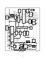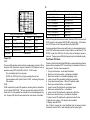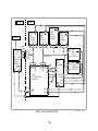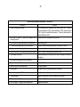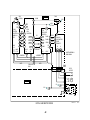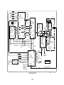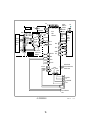
1
S ® Digital Video Player Circuit Description and Troubleshooting Course: DVD-02 Training Manual Course Description and Troubleshooting: Model: DVP-S530D Prepared by: National Training Department Sony Service Company A Division of Sony Electronics Inc. Course presented by______________________________________ Date___________________________________________________ Student Name ___________________________________________ Sony Service Company A Division of Sony Electronics Inc ©1999 All Rights Reserved Printed in U.S.A. “DTS” is a trademark of Digital Theater Systems, Inc. “AC-3” is a trademark of Dolby Laboratories Licensing Corporation. “Dolby” and “Dolby Surround” are trademarks of Dolby Laboratories Licensing Corporation. “Sony” and “Digital Cinema Sound” are trademarks of Sony. “THX” is a trademark of Lucasfilm, Ltd. Table of Contents Introduction to the DTS Audio Format 1 What is DTS? What do I need to play the DTS surround format? What do I need to play both the AC-3 and DTS surround formats? Will a 5.1 channel DTS CD play in my CD player? Why won’t my older DVD player play DTS DVDs? Can DVD movies contain both DTS and AC-3 audio tracks? How does DTS work? 2 2 2 2 3 Board Layout DVD Features Block Diagram 5 6 7 Power Supply Communications Servo Control Video and Audio Processing 7 7 7 9 3 3 Power Supply Block 11 Standby Power Supply Main Power Supply Power Consumption 11 11 11 Oscillator Frequencies 11 Standby Oscillator 13 Start Run 13 13 Regulation Concept Regulation Circuitry 13 13 Main Oscillator 15 Enable Start Run Regulation 15 15 15 15 Power Control 17 Plug In 17 Communications Block 21 Serial Data Parallel Data 21 21 Serial Data Communications 23 Serial Bus 0 Serial Bus 1 23 25 Parallel Data Communications 27 Communications from IC202 to Other ICs 29 Communications from a Destination IC to IC202 29 Mechanism 31 Disc Tray and Laser Platform Position Tilt Motor Power ON Mechanical Sequence - No Disc Power ON Mechanical Sequence - DVD Disc 31 32 34 35 Tray Motor Drive 37 Initial Sled Motor Drive 41 Manually Driving the Tilt Motor 71 Initial Sled Movement Home Position Detection 41 45 Laser Servo KHM-220A DVD Optical Block 47 49 A/V Processing Block A/V Processing Test Mode 73 75 81 DVD Focus CD Focus Three Laser Beams from One Laser Photo Detectors 49 49 50 51 Test Mode Access Tests Additional Test Mode Self-Diagnostic Function (Customer Error Codes) 81 81 83 83 Troubleshooting 85 Disc Identification 53 General Problems and Troubleshooting Guide 85 Operation 53 SACD Disc Type 53 Focus 55 Search 55 Servo Focus Drive Focus Search Communications 55 57 57 Spindle Motor 61 Kick Mode CLV PB Mode 61 63 Tracking Servo 65 Tracking Counting in Pause or Picture Jump 65 Sled Motor Drive - PB 67 Following the Track 59 Tilt Servo 69 Operation 69 1 Introduction to the DTS Audio Format Several major consumer audio formats that exist today are listed in this table: Audio Formats Year Chan Typical Typical Data Rate Compression Format (note 1) Class Used -nels sample (note 2) (Approx.) 1. Stereo 1933 2. PCM (digital version of stereo) 2 Analog linear 2 Digital 16 bits / sample. 705kbit/sec (44.1kHz sample) None DVD, LD VHS 1982 3 Analog None 4. Dolby Prologic 1987 4 Analog None 5. Dolby Digital 1991 6 Digital 7. THX 1993 1982 6 2-6 Digital Signal Source (note 3) FM, VHS, CD, LD, etc. 3. Dolby Surround 6. DTS Test Disc 20 bits / sample 384 Kbytes/sec 20 bits / sample 1,411kbits/sec 90% Prologic test CD Dolby DVD-TEST1 Dolby DVD-TEST1 VHS, theaters DTS Test CD DTS Test DVD DVD, LD, CD DVD, LD, DTV (44.1kHz sample) 75% (44.1kHz sample) Either Theaters, DVD, LD, VHS Note 1 - All formats require decoders, except Stereo and THX. THX is not a processing system but an audio/video quality control approval system. Its certification stamp means that the video and audio quality at theaters and CD/DVD discs meet uniform standards. This means the same movie viewed at one theater will not be different when viewing it at another theater. Note 2 - Data rate = bits sampled X sample rate. A CD player (44.1kHz) rate was chosen for comparison. The DVD sample rate of 48kHz would make its data rate higher than shown. Note 3 - LD = Laser Discs; DVD = Digital videodiscs; DTV = Digital TV; theaters = Movie theaters; VHS = Videotape format. Test discs can be purchased from different distributors: Prologic test CD #SSTCD · Sony parts distributors. Call 1-800-222-Sony for a distributor Dolby DVD – TEST 1 # 22707 $45. · USC Products Marketing Co.; 1 800 983 6529 DTS Test CD (digital output only) · Digital Sound Systems Entertainment 5171 Clareton Drive, Agoura Hills, Calif. 91301 1-818-706-3525 part #DTS-CD 96091 · Sony parts distributors. Call 1-800-222-Sony for a distributor CD part # J2501-154-A $7.76 list price DTS Test DVD #DTS-DVD 98061 · Digital Sound Systems Entertainment Agoura Hills, Calif. 91301 1-818-706-3525 part #DTS- DVD 98061 AC-3 decoder in the Receiver: What is DTS? Digital Theater Systems has developed a digital audio compression method similar to Dolby Digital AC-3. DTS processed audio is not as compressed as Dolby AC-3. Therefore it is said to have more surround detail (separation), envelopment and better bass because of less compression (losses). CD/DVD Player 5 Speakers 6 Channel Receiver With DTS Decoder What do I need to play the DTS surround format? And AC-3 Decoder The DTS source can be a DVD movie or CD. The DTS decoder is commonly found in the receiver. 5 Speakers Digital output preamp out to Sub Woofer Will a 5.1 channel DTS CD play in my CD player? CD/DVD Player 6 Channel Receiver Only digital noise will appear from the L/R analog outputs if not automatically muted. There will be digital output from the coaxial and optical ports. Either digital output can be fed to a DTS stand-alone decoder or a receiver with a DTS internal decoder. The DTS receiver will produce the six channels (“5.1”) or be downmixed into two (front L/R) channels depending upon the user menu. With DTS Decoder Digital output preamp out to Sub Woofer What do I need to play both the AC-3 and DTS surround formats? A DTS CD compresses the six channels of audio into the space originally occupied by the two-channel uncompressed CD audio. In order for six compressed channels to fit on a CD, the data rate must be equal to or less than the rate of a normal uncompressed CD. The AC-3 source can be DVD or HDTV (future). The decoder can be found in the player or receiver. AC-3 decoder in the Player: Data rate of an uncompressed CD per channel = 5 Speakers CD/DVD Player 6 Channel Receiver With AC-3 decoder With DTS Decoder 16 bits/sample x 44, 100 samples/second = 706 Kbytes/sec. There are two channels so the rate is doubled. Therefore the data rate of a normal stereo CD = 1,412kbit/sec. This is just about the same data rate as a DTS compressed CD. The DTS data rate is 1,411kbits, so no analog sound will be output from a DTS CD. For comparison, CD, DTS, and AC-3 data rates are shown: preamp out to Digital Output Sub Woofer Data Rate Comparison (44.1 kHz sample rate) Format 2 Output Data Rate CD Not compressed 1,412 Kbytes/sec. DTS Compressed 1,411 Kbytes/sec. Dolby Digital AC-3 Compressed 384 Kbytes/sec. 3 Why won’t my older DVD player play DTS DVDs? The DVD DTS flag was not established until Nov 1998. This flag must be inserted into the DVD’s digital coax or optical output for the receiver to recognize and decode DTS. Therefore DVD units that are not marked “DTS ready” will not play DTS even though they have digital outputs. Can DVD movies contain both DTS and AC-3 audio tracks? MDCT Time to Frequency Conversion Each single channel PCM source signal is grouped and allocated to one of 32 frequency bands for analysis. The process is commonly known as Modified Discrete Cosine Transformation (MDTC). This frequency band allocation allows for identification and removal of redundancy among the channels in the next compression stage. Coefficients Yes they can. Currently the DVD audio choices are: · · · 6 CHANNELS PCM – Producing the conventional analog L/R sound Dolby Digital or AC-3 – Compressed 5.1 channel surround sound DTS – Compressed 5.1 channel surround sound How does DTS work? Frequency Coefficients The DTS and AC-3 encoding formats are generally similar. DTS and AC3 can accept digital (PCM) audio with word lengths from 16 to 24 bits. Both encoders can accept the common 32, 44.1 and 48kHz PCM sampling frequencies, but DTS has 12 more optional frequencies. The general encoding of the DTS compression system will be explained. DTS has four blocks used to compress the PCM input audio into a single bit stream: Frequency Compression Adaptive Predictive Coding (ADPCM) PCM audio Time to 6 Channels Frequency ADPCM involves smaller support stages to: Compression Conversion 6 lines DTS Multiplexer Packer Compressed Bit Stream Sync Combine the same sounds found in other channels, Remove undetectable audio levels (below human hearing thresholds), Remove short interval noises that are swamped by louder sounds (psycho acoustic masking); and · Remove transient noises that do not repeat on the same or other channels. The support stages include transient, vector and prediction analysis stages to determine if the sound is short term, increasing or decreasing, and if the sound will repeat. Removal or the combination of sounds (compression) is determined by the analysis. · · · Multiplexer Compression Block: The six compressed channels are combined into a single line for ease of delivery. To do this each channel is stored into a register made up of flipflops. A high speed Multiplexer removes the information at six times the storage (sample) speed. Multiplexer ADPCM: From time to freq Converter • • • Transient analysis Vector analysis Prediction analysis Multiplexer Six Channels Global Bit Management Variable Length Coding N sample frequency F/F type Registers 6 lines Packer The packer organizes the information into blocks and adds: Global Bit Management · · Once compression has taken place, an examination of the six data streams for density is made. Bit groups are tagged and moved from a high-density channel to a low-density channel equalizing the amount of data. 0011100011000011111001010101 channel 1 0000001011000000000000000000 channel 3 Variable Length Coding Common fixed length codes and no data (00000000) codes are removed and replaced with shorter codes using a look up table. These shorter length code replacements are flagged for decoding. 0100011111 ROM Table 011 + flag 4 Error correction Synchronization information to each block and groups of blocks 5 BOARD LAYOUT DVD Features $ 499.00 $ 599.00 x x x x x x x x x x x x $ 899.00 $ 1,399.00 x x x x x x x x x x x x x x x x x x x x x x x x x x x x x x x x x x x x x x x x x x x x x x x x x x x x x x * MSRP = Manufacturer's Suggested List Price 6 00 77 -S VP D Audio 96kHz / 24 bit audio D/A Converter Sony Digital Cinema Sound Virtual Surround Sound Dolby AC-3 Surround Decoder DTS Decoder 2 Analog Outputs Coax & Optical Digital Outputs 1/4" Headphone Output $ 449.00 0 60 -C VP D Video 10 bit Video D/A Converter Digital RF Processor Digital Noise Reduction Video Page Bookmark 2 Composite Video Outputs 2 S-Video Outputs Component Video (Y, U, V) Outputs 0D 55 -S VP D MSRP * General Single Optical Assembly Dual Optical Assembly Active laser platform tilt servo TV / receiver / DVD Remote Advanced Test Mode Glow in the dark Remote keys Glass Epoxy Circuit Boards Anti-Resonate Chassis & tray Copper Plated Shielded Chassis 0D 53 -S VP D 0 33 -S VP D DVD Models x x x x x x x 7 Block Diagram ICs Checked During Start Up Name There are four major stages within this DVD player. They operate in this sequence to produce the discs’ video and audio: · · · · Power Supply Communications Servo Control Video and Audio Processing Power Supply The power supply block delivers five different voltages. Ever 5V is the only voltage present when the unit is plugged into AC. Ever 5V powers Interface IC201 to switch on the remainder of the voltages when it receives the power ON (P Cont) command. Communications Plug In At plug in, Interface IC201 powers on the unit for 1.3 seconds, keeping the display dark. During this time there is a brief communication between Interface IC201 and System Control IC202 on the serial bus. At the conclusion of this communication “handshaking”, the front panel Dolby Digital indicator lights and quickly extinguishes as the unit powers off. The front panel red standby light is on during the entire initial communication, never turning green when momentarily powering up at plug in. Power ON At power ON, the red standby light turns to green and the power supply is turned on. After another brief communication between IC201 and IC202, IC202 retrieves and implements the start up program stored in Flash Memory IC205. The start up program requires IC202 to check for the presence of these six ICs on the parallel bus and IC501 on the serial bus: Number Purpose 1. Flash ROM IC205 Start up program instructions 2. Hybrid Gate Array IC601 Expansion port for System Control IC202 to indirectly communicate with others on the parallel bus. 3. SRAM IC204 IC202’s local memory 4. AV Decoder IC401 Audio (AC-3) and Video (MPEG 2) decoder 5. ARP2 IC303 CD/DVD data processing and separation 6. Servo IC701 Analog servo control Dolby Prologic, Rear channel delays, 5.1 channel downmixing to 2 channels If an IC does not reply, IC202 instructs IC201 to power off the set. 7. Audio DSP IC501 Servo Control At the successful conclusion of the start up program, IC202 retrieves servo parameter data from EEProm IC201 using the serial bus. Then IC202 communicates with expansion port HGA IC601. IC601 relays the information to other ICs connected to it. One of those ICs is IC701. Servo IC701 is instructed to reset the base unit mechanism to the initial position and confirm it: · Tray closed · Tilt servo at mid position · Sled returned to home position If the initial position is not confirmed before a time limit (“time out”), IC201 will power off the set. Confirmation comes from IC701 through IC601 to IC202. IC202 then sends commands back to servo IC701 for disc detection. SPINDLE CONTROL IC802 MECHANISM OPTICAL DEVICE DVD DATA TK-51 BD. RF IC001 RF AMP LD FE TE PI FOCUS COIL TRACK COIL M RF IC801 FOCUS & TRACKING COIL TILT MOTOR DRIVER IC401 AV DECODER SPINDLE M CD DATA, CLK IC701 SERVO IC802 SPINDLE, SLED, & LOADING MOTOR DRIVER 3.3V LOADING VIDEO BUFFERS IC501 AUDIO DSP DIGITAL AUDIO OUT ANALOG AUDIO IC902 OUT DAC IC905-7 DAC 5.1 CH AC-3 OUT IC204 SRAM IC202 SYSTEM CONTROL IC601 HGA COMPONENT V OUT COMPOSITE V OUT PARALLEL BUS IC205 FLASH MEM SERIAL BUS SPINDLE CONTROL IC303 SLED M Y,Pb, Pr Y SPDIF, ACHI-6, CLK TILT M S VIDEO OUT Y,C IC303 ARP2 S. DATA CLK AU212 BD. IC402 IC403 SDRAM IC304 DRAM IC201 EEPROM MB-85 BD. EVER 5V POWER BLOCK IR REC 5V 12V -12V IC201 INTERFACE MICRO FR150 BD. DISPLAY FL101 BD. PANEL SWITCHES P CONT. BLOCK DIAGRAM 8 1DVD02 1146 6 22 99 9 Video and Audio Processing After the servos have begun, RF data will come from the optical assembly within the base unit. The “eye pattern” RF data is split into two paths to provide: 1. Feedback signal to lock the servos; and 2. Video and audio information. In the A/V processing chain, the RF data is processed by the following ICs: Audio / Video Processing ICs Name IC Audio or Video RF Amp IC001 A/V (both) ARP2 IC303 A/V (both) Decoder DSP IC401 IC501 A/V (both) A DAC IC902 A DACs IC905IC907 A Purpose Matrix the optical outputs to produce signals for servo and A/V circuits • 16 to 8 bit Demodulation • Descrambles the main data using external memory IC304 • Generates bit clock Video • MPEG decompression using the external IC402 and IC403 memories • Crops the 16x9 image for a 4x3 TV picture • Controls spindle motor speed • Sends disc’s control and menu data to IC202 • On screen display graphics • D/A Converter (analog video output) Audio • MPEG audio decompression • Dolby Digital AC-3 decompression using external SRAM IC402 / IC403 • Sound enhancements when there is no AC-3 received (Rear channel delay) • Downmixing of 6 channel AC-3 into 2 (L/R) channels • Dolby Prologic decoding • Digital coax and optical output • Rear channel delay • Front/rear level balancing • Test tone generation Digital to analog converter for the front left and right channels 3 Digital to analog converters for the six AC-3 channels SPINDLE CONTROL IC802 MECHANISM OPTICAL DEVICE DVD DATA TK-51 BD. RF IC001 RF AMP LD FE TE PI FOCUS COIL TRACK COIL M RF IC801 FOCUS & TRACKING COIL TILT MOTOR DRIVER IC401 AV DECODER SPINDLE M CD DATA, CLK IC701 SERVO IC802 SPINDLE, SLED, & LOADING MOTOR DRIVER 3.3V LOADING VIDEO BUFFERS IC501 AUDIO DSP DIGITAL AUDIO OUT ANALOG AUDIO IC902 OUT DAC IC905-7 DAC 5.1 CH AC-3 OUT IC204 SRAM IC202 SYSTEM CONTROL IC601 HGA COMPONENT V OUT COMPOSITE V OUT PARALLEL BUS IC205 FLASH MEM SERIAL BUS SPINDLE CONTROL IC303 SLED M Y,Pb, Pr Y SPDIF, ACHI-6, CLK TILT M S VIDEO OUT Y,C IC303 ARP2 S. DATA CLK AU212 BD. IC402 IC403 SDRAM IC304 DRAM IC201 EEPROM MB-85 BD. EVER 5V POWER BLOCK IR REC 5V 12V -12V IC201 INTERFACE MICRO FR150 BD. DISPLAY FL101 BD. PANEL SWITCHES P CONT. BLOCK DIAGRAM 10 1DVD02 1146 6 22 99 11 Power Supply Block The power supply is on a single board located to the left of the DVD mechanism. This board contains both the standby and the main power supply. The input line filter L101 and the board connectors are the only parts that are not available. Standby Power Supply This power supply produces Ever 5V as long as AC is present. Ever 5V is supplied to interface IC201 (MB85 board) and the mute transistors (AU212 board). The standby power supply consists of an oscillator and an error regulator. The oscillator consists of switch Q121 and a control transistor Q122. The oscillator output is applied to T102. T102’s secondary is rectified to output Ever 5V. Regulation The Ever 5V voltage regulation circuit uses: · IC202 – error detector · PC121 – photocoupler · Q122 – control transistor. IC202 samples the Ever 5V output and produces a correction voltage. Photocoupler PC121 passes the error voltage from the cold ground circuit to the hot ground side circuit. The control transistor Q122 receives the error voltage and uses it to alter the base bias of switch Q121. The change in bias alters the off time of the oscillator signal. This changes the oscillator frequency. The changes in frequency affect the efficiency of the transformer, which regulates the Ever 5V. Main Power Supply The main power supply works similarly to the standby supply except the main supply is switched, handles more power and has multiple secondaries. The main power supply is switched ON by PCONT from the Interface IC on the FR148 board. A high at PCONT enables switch Q101 to begin oscillating. Transformer T101 produces several output voltages that are rectified into DC for the remainder of the DVD unit. When a shorted spindle motor driver IC802 loaded the unfused +12V supply line, the main oscillator quit. The oscillator worked again when the short was removed. Regulation The 3.3Vdc output is used to regulate the main power supply. Error detector IC201 receives the 3.3Vdc and produces a correction voltage. If the input voltage increases, the error detector output decreases. The PC101 photocoupler passes the correction signal to the control transistor Q102. Q102 adjusts the off time of the oscillator signal to correct the 3.3Vdc output the secondary. If the DVD power consumption is normal, the remainder of the T101 outputs will be correct. Power Consumption The current along each supply line was measured in both the idle and the DVD disc playback mode. Model DVP-S530D Current Consumption Part replaced Supply line Current by Ammeter Idle Disc PB Ever 5V L205 30ma (set off) 77mA (set on ) +12V partial PS201 196mA 198mA +12V total L201 236mA 350-700mA +5V PS202 281mA 305mA +3.3V PS203 * 894mA 950mA -12V PS204 129mA 130mA * Use short ammeter leads or the unit will not PB the disc and the display will not come on. The PS203 current without the display will only be 580mA. Oscillator Frequencies Power Supply Oscillator Frequencies Power Supply Set Off Set On (stop mode) Standby (Q121/D) 57.45kHz 49.65kHz Main (Q101/C) 0 101.2kHz SRV902UC BOARD L201 +12V PS201 +5V CN201 4 PS202 Q101,102,T101 MAIN OSC. +3.3V 2 PS203 1 PS204 6 -12V D101-104 +3.3V -12V TO AU212 BD. ANALOG AUDIO/ VIDEO 7 CN202 2 L101 LINE FILTER +5V EVER 5V RV201 PC101 PHOTO COUPLER +12V IC201 ERROR DET. 1 5 M+12V A+12V +5V TO MB 85 BD. SERVO CONTROL 6 +3.3V 7 PC102,Q201 POWER CONTROL CN203 1 3 5 Q121,122,T102 STBY OSC. EVER 5V PCONT +5V -12V EVER 5V L205 TO FR148,FL101 BDS. INTERFACE/ DISPLAY 2 F101 PC121 PHOTO COUPLER 1 2 IC202 ERROR DET. CN101 POWER SUPPLY BLOCK 12 2DVD02 1137 4 27 99 13 Standby Oscillator The standby oscillator produces Ever +5 volts when the DVD player is plugged into 120VAC. This Ever 5V is applied to the Interface IC201 (on the circuit board behind the front panel) and the audio and video mute transistors (on the rear board). The standby oscillator stage consists of two transistors and a transformer. Regulation is performed using the Ever 5V output to control the off time of the oscillator cycle. The standby oscillator has three operational parts: · Start · Run · Regulation Start At AC plug in, the standby oscillator stage begins when R122 and R123 bring the FET Q121 gate voltage from 0 to about 1volt. This turns on the low power FET, allowing it to pass Drain to Source current and complete T102’s primary circuit path to hot ground. Run Oscillator transistor Q121 turns ON As current flows in T102’s upper left primary winding, a voltage is induced in the lower secondary winding that will keep FET oscillator Q121 turned ON. A positive voltage from the lower secondary winding takes two paths. The first path is through R126, R125 and C121 to Q121’s gate. This keeps Q121 conducting. The second path is through R127 and R128 to Q122’s base. Q122’s collector is connected to the oscillator’s gate. As a result, Q122 becomes an active resistor. Q122’s conduction prevents the gate voltage from rising too high (protection) and later we will see that it is used for regulation. Oscillator transistor Q101 turns OFF When Q101 is saturated, there is no longer a change in T102’s primary current. The voltage induced into the lower secondary winding decays. This reduction in bias voltage permits Q121 to turn OFF. With Q121 OFF, the magnetic field in T102’s primary winding collapses, causing current flow thorough C123 and limiter R130. The collapsing magnetic field induces a negative voltage into the lower secondary winding. The negative voltage takes two paths to reset the oscillator. The first path is through R126, R125 and C121 to keep oscillator transistor Q121 OFF. The second path is through D121 and R128 into the base of Q122. This turns off transistor Q122 in preparation for the next oscillator cycle. Regulation Concept Regulation of the Ever 5V line is accomplished by sampling the output voltage and using it to reduce the off time of the oscillator. By reducing the off time, the total oscillator cycle is reduced. Shortening the time it takes to complete a cycle means its frequency is increased. This oscillator signal is applied to transformer T102. A transformer has an optimum frequency that will allow maximum power transfer (at resonance). When the applied oscillator frequency is above resonance, the efficiency drops and its secondary voltage is reduced. By varying the applied frequency, the output voltage can be regulated. Regulation Circuitry IC202 is the error regulator for this stage. Voltage divider R212, R209 and R210 reduce the Ever 5V so there is 2.5V at IC202’s input. This allows its operation in the linear region. IC202’s output (collector) is inversely proportional to its input. The collector output is connected to the opto-isolator diode that passes the error signal to the hot ground oscillator circuit. If the Ever 5V increased, the opto-isolator transistor would conduct more, reducing the resistance between the lower secondary winding and Q122’s base. The reduced resistance allows more current to flow, permitting Q122 to turn on sooner. The sooner it turns on, the sooner the FET turns off, increasing its frequency of operation that results in a reduced output voltage for regulation. IMPORTANT VOLTAGES MEASURED WITH THE SET OFF: Voltage DC Voltage Q101/Drain 300Vp-p 166V Q101/Gate 13.8Vp-p 2V D121/Anode 16Vp-p 0V MAIN OSC D101-D104 R121 T102 C123 R122 C108 220 Q121 R123 D206 L205 5V CN203 2 C102 + S C121 L101 LINE FILTER R130 D R124 C210 100 D208 CN201 R125 7 Q122 R128 22k R126 + C211 100 EVER 5V TO FR150 BD. (DISPLAY) EVER 5V TO AV212 BD. (MUTE) R127 D121 R129 100 OHM R206 470 OHMS D122 R212 R207 1k PC121 ON3131 C212 4.1V R209 R208 2.5V IC202 AN1431 R210 STANDBY OSCILLATOR 14 29DVD02 1175 6 28 99 15 Main Oscillator Run Q101 Turns ON The main oscillator stage operates like the standby oscillator stage except that the main oscillator is switched ON/OFF and there are multiple secondaries to supply the needs of the DVD player. The main oscillator has four parts: · · · · Enable Start Run Regulation Enable Oscillator OFF The operation of the main oscillator is inhibited by PC102. When the unit is plugged into AC, Ever 5V is made by the standby oscillator stage and is used to turn on the opto-isolator LED in PC102. The LED’s infrared light turns on the phototransistor and it conducts. PC102’s phototransistor is connected to oscillator transistor Q101’s start voltage applied to the base. When PC201 conducts, the start voltage from R102/R103 is grounded, stopping the oscillator. Oscillator ON Q201 removes the voltage to the opto-isolator diode in PC102, permitting the main oscillator stage to run. When PCONT from Interface IC201 goes high at CN203/pin 1, Q201 turns ON. Its conduction grounds the voltage from R211, removing voltage from the LED. PC102 transistor turns off, removing the ground from R103 so the main oscillator transistor Q101 can start. Start Once the PCONT control line at CN203/pin 1 goes high, PC102’s transistor no longer conducts. The ground is removed from the start voltage at the junction of C111 and R104 so it rises. It will reach 6.6V, limited by the voltage divider formed by R102, R103 and R104. Sufficient current passes through C111 during this voltage increase to turn ON main oscillator Q101. This is how oscillator transistor Q101 starts conducting (turns ON) and the main oscillator starts. When Q101 turns ON, current flows through the main transformer’s primary winding at the upper left of T101. This induces a positive voltage to the lower T101 winding that follows two paths. The first path is through R106, R107, D109 and C113 to Q101’s base to keep it conducting. The second path is through D108 and R109 to bias Q102. Q102 acts like an active resistor at Q101’s base to keep the voltage from becoming excessive (protection) and is used later for regulation. Consequently the correct value components and transistors are critical. When Q101 reaches saturation, there is no longer a change in T101’s primary current. The steady current flow no longer induces a voltage into the lower secondary winding and the secondary voltage decays. Q101 Turns OFF The reduction in secondary voltage turns Q101’s OFF. The magnetic field in T101’s primary collapses. D105, limiter, L102 and C110 short its energy. D106 is used to discharge C110 (when Q101 is ON). The collapsing (changing) magnetic field induces a negative voltage at the lower secondary winding. This negative voltage from T101 passes through R106, R107 and C113 to the base of oscillator transistor Q101. It is used to cut off Q101 to conclude this oscillator cycle. Regulation The 3.3-volt output is monitored by error regulator IC201 and used to control the conduction of phototransistor PC101. If the 3.3-volt line rises, the phototransistor conducts harder. This reduces the resistance between the lower secondary winding and Q102’s base, increasing Q102 base current. The increased base current drives Q102 harder, lowering the oscillator’s base bias voltage and causing the oscillator to be turned OFF sooner. When part of the oscillator waveform is shortened, its frequency increases. This reduces T101 efficiency and the 3.3V output voltage is returned to normal. IMPORTANT VOLTAGES: Q101/Collector = 336Vp-p; 150Vdc. PC101/collector = 2.6Vdc. PC101/emitter = 0.21Vdc Feedback secondary voltage at D108/cathode = 20Vp-p; 0.21Vdc. CN202 2 M+12V 6 STBY OSC 7 T101 D201 PS201 0.5A L201 5 +5V 1 A+12V CN201 4 D105 L105 C110 +12V C202 PS202 D202 R102 TO MB85 BD. R213 AC C201 +3.3V 2 +5V C203 C111 4.7mF R103 D110 L102 D106 Q101 D203 L202 TO AV212 BD. 1A PS203 L203 1 +3.3V 6 -12V RV201 3.3V ADJ. R104 C113 PS204 0.75A D204 D108 MTZJ3.0 Q102 D109 R106 47 1W R109 R107 R204 2.5V R205 R201 D107 R203 EVER 5V PC101 ON3131 IC201 AN1431 C205 4V R211 Q201 P CONT 1 PC102 ON3131 FROM FR150 BD. CN203 MAIN OSCILLATOR 16 30DVD02 1174 7 12 99 17 Power Control Plug In When the DVD player is plugged into AC, the power supply only outputs Ever 5V to: · Analog audio mute transistors – AU-212 board · Interface IC201/pin 16 – FL101 board · Reset IC202/pin 5 - FL101 board The mute transistors are biased ON to keep the 5.1, headphones and L/ R channel audio outputs grounded. 10. Interface IC201 brings PCONT low, removing power to the set. Unit is now in standby and ready to be powered ON. IC201 – IC202 Communications Waveforms The following sets of waveforms show this communication between IC201 and IC202. Notice that the Dolby Digital LED is turned ON only at the conclusion of the plug in communications. The LED does not light when there are incomplete communications. PM3394, FLUKE & PHILIPS ch1 T 1 ch2 ch3 2 Ever 5V applied to Interface IC201 starts the 4MHz X201 crystal connected to pins 14 and 15. ch4 3 Reset IC202 on the FL101 board uses C211 to hold its pin 4 momentarily low when Ever 5V is first applied. This resets Interface IC201/pin 18. After reset, a brief communication occurs between IC201 and IC202. A momentary light of the front panel blue Dolby Digital LED (D203) marks the end of the plug in communications and the unit shuts down. The plug in sequence is listed below: 1. 2. 3. 4. 5. 6. AC plug in Ever 5V is applied to Interface IC201/pin 16 X201 becomes active and stays active Red power off/standby LED comes ON. PCONT from Interface IC201/pin 24 goes high to power the set Ready pulse is output IC201/pin 78 as an interrupt line to IC202 to begin communications. It is difficult to see this low going interrupt pulse on a a scope, but it will light a scope’s “triggered” LED. 7. IC601 transfers this “ready” (interrupt) information to System Control IC202 by using another interrupt signal from IC601/pin 155 (low going). The low forces IC202 to generate a chip select (CS1 or CS4) so the data can be transferred to IC202 on the parallel bus. 8. System Control IC202 sends chip select (difficult to see the low going pulse from pin 97), bit clock (low pulses from pin 78) and serial data (high pulses from pin 77) to Interface IC201. 9. IC201 acknowledges by lighting the Digital Dolby LED D203 CH1!5.00 V= 4 CH2!2.00 V= CH3!5.00 V= CH4!5.00 V= CHP MTB 200ms- 0.40dv ch1+ Plug in Communications – between IC201 / IC202 Name Location Voltage/div Channel 1 PCONT CN203/pin 1 5Vp-p Channel 2 Dolby Digital LED D203/anode 2Vp-p Channel 3 CS from IC202 CN006/pin 3 5Vp-p Channel 4 Data from IC201 CN006/pin 4 5Vp-p Time base 200msec/div. The following second set of waveforms is taken of IC202 CS signal (ch 3) that is replying to IC201. Notice that the return clock (ch 3) and data (ch 4) from IC202 occur before IC201 turns the LED (ch 2) ON. IC202 RESET PST9140 FR150 EVER 5V 5 5 CN201/ CN002 3 4 C211 R274 2 IC051 1 IR RECEIVER 16 4 30 CN202/ CN006 SIN 72 5 9 IC201 INTERFACE CONTROL M38857 MCHE206FP GRN R072 6 31 7 32 R071 MB85 BD. 14 IC203 BUFFER SN74 HCT08 R285 18 3 5V D203 DOLBY DIGITAL 3 3.3V 1 43 SCLK 70 6 6 4 3 71 4 12 11 SRDY1 78 5 14 15 69 70 2 24 97 93 IC202 SYSTEM CONTROL 11 76 MB91101 R045 SI0 PFV CS4 CS1 R044 RED 78 SC0 CSOL SBUSY1 76 S OUT EVER 5V 4 77 SO01 7 R036 CE 10 37 47 26 IC205 FLASH ROM MBM29 LV160 R221 3 S071 POWER R222 X201 4MHz FRONT PANEL BUTTONS S212-S218 12 2 DISPLAY 142 22 R037 FL101 BD. 3.3V 1 3.3V SRV902UC PWR BLK 1 6 P CONT. EVER 5V PARALLEL BUS PARALLEL BUS 5V 2 3.3V 20 5 5V 40 CS4 XIF INT 141 CS1 IC601 HGA CXD8788Q CN202 CN001/ POWER CONTROL 18 13DVD02 1154 6 22 99 19 PM3394, FLUKE & PHILIPS Power ON IC check sequence (not shown in the diagram) ch1 T Chip Select Source 1 ch2 ch3 2 ch4 3 CH1!5.00 V= 4 CH2!2.00 V= CH3!5.00 V= CH4!5.00 V= CHP MTB 200ms- 0.40dv ch1+ Plug in Communications – between IC201 / IC202 Name Location 1. CS 1 - IC202/pin 10 SRAM IC204 / HGA IC601 2. CE – IC202/pin 11 Flash ROM IC205 3. CS 3 – IC202/pin 8 AV Decoder IC401 4. CS 4 – IC202/pin 7 HGA IC601 5. CS 2 – IC202/pin 9 AV Decoder IC401 6. XCS – IC601/pin 111 ARP2 IC303 7. HCS - IC601/pin 118 Servo IC701 Voltage/div Channel 1 PCONT CN203/pin 1 5Vp-p Channel 2 Dolby Digital LED D203/anode 2Vp-p Channel 3 Bit clock from IC202 CN006/pin 6 5Vp-p Channel 4 Data from IC202 CN006/pin 5 5Vp-p Time base Destination IC 200msec/div. Power ON IC201 The power ON operation works much like a modern day computer. When the power ON command is received, Interface IC201 begins a boot up sequence using IC202 and IC205 to finish it. IC201 causes: · The red standby light to turn to green; · PCONT (at IC201/pin 24) to go high, powering the set; and · Communications with System Control IC202, continuing the power ON operation IC202 IC202 continues the power ON operation, retrieving start up information from the Flash ROM IC205. This start up information instructs IC202 to check each IC on the parallel bus and wait for an acknowledgement signal. At power ON, these ICs are polled in the order shown in the table: When all the replies have been received, Interface IC201 is informed and IC201 keeps the unit powered ON (PCONT remains high). At the same time, IC201 turns on the front panel blue Dolby Digital LED. If a communications failure occurs and there is no acknowledgement signal to IC202 within three seconds of power ON, the unit will turn off. The PCONT signal (from IC201/pin 24) will go low and the player power is removed. The green power ON light changes back to red (standby mode). Post Power ON Check Therefore, if the blue Dolby Digital LED lights, communications have taken place and the unit remains ON. The next step is to determine if there is a disc present. The disc check sequence is: 1. Tray up and chucked – chuck switch feedback 2. Sled moves to home position – photosensor feedback 3. Sled moves outward – no feedback (stepping motor) 4. Laser is turned ON momentarily while focus searching 5. Focus Search is performed – FE and PI feedback signal 6. Sled moves outward further – no feedback 7. Laser is turned ON and Search is performed again 8. Sled moves outward further – no feedback 9. Laser is turned ON and Search is performed a third time 10. Sled moves inward to home – photosensor feedback 11. Laser is turned ON and Search is performed a fourth time 12. Spindle motor rotates – FG amp kick drive feedback 13. Display reads NO DISC. If an IC fails to receive the correct feedback from its sensors, System Control will instruct IC201 to enter standby (red front panel light). IC202 RESET PST9140 FR150 EVER 5V 5 5 CN201/ CN002 3 4 C211 R274 2 IC051 1 IR RECEIVER 16 4 30 CN202/ CN006 SIN 72 5 9 IC201 INTERFACE CONTROL M38857 MCHE206FP GRN R072 6 31 7 32 R071 MB85 BD. 14 IC203 BUFFER SN74 HCT08 R285 18 3 5V D203 DOLBY DIGITAL 3 3.3V 1 43 SCLK 70 6 6 4 3 71 4 12 11 SRDY1 78 5 14 15 69 70 2 24 97 93 IC202 SYSTEM CONTROL 11 76 MB91101 R045 SI0 PFV CS4 CS1 R044 RED 78 SC0 CSOL SBUSY1 76 S OUT EVER 5V 4 77 SO01 7 R036 CE 10 37 47 26 IC205 FLASH ROM MBM29 LV160 R221 3 S071 POWER R222 X201 4MHz FRONT PANEL BUTTONS S212-S218 12 2 DISPLAY 142 22 R037 FL101 BD. 3.3V 1 3.3V SRV902UC PWR BLK 1 6 P CONT. EVER 5V PARALLEL BUS PARALLEL BUS 5V 2 3.3V 20 5 5V 40 CS4 XIF INT 141 CS1 IC601 HGA CXD8788Q CN202 CN001/ POWER CONTROL 20 13DVD02 1154 6 22 99 21 Communications Block Both serial and parallel bus structures are used in the same unit of today’s DVD players. The serial data bus is a simple way to provide communications between ICs. On one line, data is transmitted one bit after another to the next IC in 8, 16, 20, 24 or 32 bit groups. On another line, corresponding clock pulses accompany the bits of data. One clock pulse identifies each bit of data - this is why this line is also called a bit clock. Therefore, it takes 8, 16, 20, 24 or 32 clock pulses to receive a group of data in a serial bus. A parallel data bus is used when large amounts of data need to be transmitted in a shorter time frame. In the parallel bus, multiple data lines are used along with a clock line. When a single clock pulse is sent, the 8, 16, 20, 24 or 32 lines each simultaneously transmit a bit of data to the receiving IC. (Only 16 data lines are used here.) Therefore, it takes only one clock pulse to receive a group of data in a parallel bus. The parallel bus is used in processing video information (IC401) and in the disc playback servo (IC701) where large amounts of data must be handled quickly. Serial Data The serial data bus connects several ICs and consists of two or three lines. Serial data is transmitted from one IC to another on a unidirectional line (arrows shown in one direction). This data is accompanied by a clock signal for a total of two lines in a unidirectional serial communication. The interface control IC201 and System Control IC202 communicate bidirectionally (arrows shown in two directions). Three lines are necessary when bi-directional transmissions are called. There is a data line for each direction. The additional clock signal makes a total of three lines for a bi-directional serial bus. The clock signal usually comes from the controlling micro, which in this case is System Control IC202. System Control IC202 communications with Interface IC201, EEProm IC201 and DSP IC501 are bi-directional. System Control communications to the Digital to Analog Converters (DAC) IC902, IC905-7 are unidirectional. Parallel Data The parallel data bus is much more complicated than the serial bus. It consists of address lines, data lines and a clock line. Just before data is transmitted from one IC to another, a location is designated using address lines. Then clock pulses are sent from the master IC202 to transfer the data into the receiving IC. When communications are bi-directional on the parallel bus, an additional line identified as write enable (WE) and/or read enable (RE) is used. These lines determine the direction of the data to or from the master IC. When there is no WE or RE line, the bi-directional data communication is preestablished first as read-data from the master micro. Write-data occurs afterwards. CS FROM IC601 IC201 INTERFACE CONTROL IC201 4k EEPROM CS FROM IC202 CS FROM IC202 IC902 AUDIO 2 CH DAC IC501 AUDIO DSP CS FROM IC202 IC905 DAC FRONT CS FROM IC601 IC906-7 DAC REAR, CENTER SERIAL BUS CS CHIP SELECTS CS FROM IC202 IC202 SYSTEM CONTROL CS FROM IC202 CS FROM IC202 IC205 FLASH IC204 SRAM IC601 HGA CHIP SELECTS CS FROM IC601 IC701 SERVO PARALLEL BUS CS FROM IC202 IC401 AV DECODE IC303 ARP2 COMMUNICATIONS BLOCK 22 CS FROM IC601 6DVD02 1149 6 23 99 23 Serial Data Communications A close examination of the serial bus structure shows there are two serial buses. Both are active as long as the set is ON. IC202/pins 76 and 77 to occur. The entire operation is similar to someone working when interrupted by a doorbell. When he is ready, he will answer the door. Afterwards he returns to his work in the house or elsewhere. The IC201 to IC202 communications sequence is: System Control IC202 and Interface IC201 Data Transfer Sequence Serial Bus 0 Name of Signal Serial Bus 1 1. SRDY (ready) IC201pin 78 Request communications 2. CSOL (chip select) IC202/pin 97 Communications window (active low) 3. SC0 (clock) IC202/pin 78 Serial clock for data 4. SI0 (data) IC201/pin 71 User commands 5. SO0 (data) IC202/pin 77 Display update 6. CSOL (chip select) IC202/pin 97 Communications ends (returns high) Serial Bus 0 Bus 0 is used for bi-directional communications between: · System Control IC202 · Interface IC201 · EEProm IC201 System Control IC202 is the master IC. It sends and receives data on the serial data in (SI0, at IC202/pin 76) and out (SO0, at IC202/pin 77) lines. The data is always accompanied by serial clock (SC0, at IC202/pin 78) from IC202. There are always communications between these two ICs as long as there is power applied. Interface IC201 System Control IC202 has the continuous task of transferring display information to the Interface IC201. The Interface IC201 must inform System Control IC202 that there is a new command such as play or stop. Communications begin when Interface IC201/pin 78 outputs a low going “ready” pulse. In this IC the ready command is more like an interrupt command. This low going pulse is received by IC601/pin 22, which is used as an expansion port to access System Control IC201 via the parallel bus. The interrupt input is periodically checked within IC202’s program. When found, IC202 will enter a subroutine and acknowledge IC201’s request to send data for processing. System Control IC202 acknowledges the interrupt signal by outputting two signals: a low chip select signal from pin 97 and a clock signal from pin 78. This allows for data communications on the SI0 and SO0 lines at Signal Source Signal purpose EEProm IC201 During playback or when playback is started, System Control IC202 retrieves information held in EEProm IC201. IC201 holds servo data and stores some disc parameters, such as how many information layers are on the disc. Some of this data is visible in the test mode. Bi-directional communications between System Control IC202 and EEProm IC201 is accomplished using: · Two single direction serial data lines (SO0 and SI0) · Clock pulses from IC202/pin 78 · Chip Select signal from IC601/pin 23 Periodically in IC202’s routine, EEProm IC201is chip selected (when pin 3 is brought low). When this occurs, data is transferred between the ICs on the data lines (SO0 and SI0). FL101 BD. MB85 BD. IC201 CS 4k EEPROM AK6440AF SC0 SO0 SI0 DISPLAY 4 5 CSO 28 IC902 AUDIO 2 CH DAC CXD8799N 62 3 6 IC501 CS AUDIO DSP CDX1901R SC1 SI1 SO1 SC1 SO1 63 27 26 66 61 IC905 FRONT CS2 28 L/R DAC CXD8799N SC1 SO1 27 CN202/ CN006 SIN 1 S OUT 1 72 71 SC1 70 IC201 INTERFACE CONTROL M38857MCH 4 SI0 SERIAL BUS 1 76 S BUSY SRDY 78 IC906 27 SC1 CS2 28 REAR L/R DAC 26 SO1 CXD8799N 5 SO0 6 SC0 77 79 80 89 78 SC0 76 SC1 10 SI1 SI0 SO0 SO1 7 IC601 HGA CXD8788Q CS1 CS4 141 142 XDACS2 96 OICS 28 PARALLEL BUS XFMCS 97 CSOL IC907 CS3 28 27 SC1 CENTER WOOFER DAC 26 SO1 CXD8799N XDACS3 97 IC202 SYSTEM CONTROL MB91101PFV 3 26 PB3 99 PB2 98 XIFINT XECS 23 22 2 XIF BUSY SERIAL DATA COMMUNICATIONS 24 4DVD02.DWG 1144 6 23 99 25 Serial Bus 1 Bus 1 is used for communications between: · System Control IC202 · Audio DSP IC501 · Audio 2 channel IC902 · Front, Rear, and Center D/A converters IC905 to IC907 System Control IC202 is the master IC. It sends and receives data on the serial data in (SI1, at IC202/pin 79) and out (SO1, at IC202/pin 80) lines. The data is always accompanied by serial clock (SC1, at IC202/pin 89) from IC202. There are always communications present at IC202/pins 79,80 and 89 as long as there is power applied just like in serial bus 0. Audio DSP IC501 Bi-directional communications between System Control IC202 and IC501 is similar to that with EEProm IC201. Communications between System Control IC202 and Audio DSP IC501 are accomplished using: · Two serial data lines (SO1 and SI1) · Clock from IC202/pin 89 · Chip Select from IC601/pin 28 Periodically in IC202’s routine, Audio DSP IC501 is chip selected. When the chip select pin 62 line is brought low, data is transferred between the ICs on the data lines (SO1 and SI1). Audio 2 Channel D/A Converter IC902 Audio Front, Rear, and Center D/A Converters IC905 - IC907 System Control IC202 communicates with the remainder of the ICs on the serial bus 1 lines in a unidirectional manner. Each one of these D/A Converters has an individual chip select line from IC601. The SO1 data line from IC202/pin 80 is common to the D/A Converters. Data applies only to the D/A Converter when its chip line is low. The data as always is accompanied by bit clock from IC202/pin 89. IC Function IC Name Number Function System Control IC202 Main Micro Interface IC201-FL101 Bd Accepts user commands (play, open tray, next, etc) EEProm IC201-MB85 Bd Stores servo info Audio DSP IC501 Delays (echoes) for speaker effects Audio 2 channel D/A Converter IC902 D/A Converter for analog audio Front, Rear, Center, D/A Converter IC905 - IC907 D/A Converter for 5.1 AC-3 signal. FL101 BD. MB85 BD. IC201 CS 4k EEPROM AK6440AF SC0 SO0 SI0 DISPLAY 4 5 CSO 28 IC902 AUDIO 2 CH DAC CXD8799N 62 3 6 IC501 CS AUDIO DSP CDX1901R SC1 SI1 SO1 SC1 SO1 63 27 26 66 61 IC905 FRONT CS2 28 L/R DAC CXD8799N SC1 SO1 27 CN202/ CN006 SIN 1 S OUT 1 72 71 SC1 70 IC201 INTERFACE CONTROL M38857MCH 4 SI0 SERIAL BUS 1 76 S BUSY SRDY 78 IC906 27 SC1 CS2 28 REAR L/R DAC 26 SO1 CXD8799N 5 SO0 6 SC0 77 79 80 89 78 SC0 76 SC1 10 SI1 SI0 SO0 SO1 7 IC601 HGA CXD8788Q CS1 CS4 141 142 XDACS2 96 OICS 28 PARALLEL BUS XFMCS 97 CSOL IC907 CS3 28 27 SC1 CENTER WOOFER DAC 26 SO1 CXD8799N XDACS3 97 IC202 SYSTEM CONTROL MB91101PFV 3 26 PB3 99 PB2 98 XIFINT XECS 23 22 2 XIF BUSY SERIAL DATA COMMUNICATIONS 26 4DVD02.DWG 1144 6 23 99 27 Parallel Data Communications Chip Select Signals from IC202 (active low) CS Source There are six ICs that communicate with System Control IC202 on the parallel bus: ICs on the Parallel Bus Name Number Purpose Pulse Width/Polarity Destination 1. CS 1 - IC202/pin 10 SRAM IC204 / 0.56us /– HGA IC601 0.9usec/- 2. CE – IC202/pin 11 Flash ROM IC205 0.56us /– 1. Flash ROM IC205 Start up program instructions 3. CS 2 – IC202/pin 9 AV Decoder IC401 2. Hybrid Gate Array IC601 Expansion port for System Control IC202 0.7 & .26 usec/- 4. CS 4 – IC202/pin 7 HGA IC601 0.3usec/- 3. SRAM IC204 IC202’s local memory 5. CS 3 – IC202/pin 8 AV Decoder IC401 1.2usec/- 4. AV Decoder IC401 Audio (AC-3) and Video (MPEG 2) decoder 6. XCS – IC601/pin 111 ARP2 IC303 0.3usec/- 7. HCS - IC601/pin 118 Servo IC701 0.3usec/- 5. ARP2 IC303 CD/DVD data processing & separation Chip Select Waveforms 6. Servo DSP IC701 Analog servo control The following waveforms show the chip select signals going to the S RAM IC204 (ch 1) and AV Decoder IC401 (ch 2 and 3). They can be compared to the D1 data (ch 4) to show that the chip select (ch 1-3) signals occupy more than one bit clock interval. Note that on each of the CS 1 (ch 1) and CS 2 (ch 2) lines, two different pulse widths are used. These waveforms were taken with the unit on without a disc being played. Bi-directional communications between these ICs are accomplished using the following lines; however, not all ICs use the last three lines: · · · · · · Chip Select from IC202 Address from IC202 Data (bi-directional) Clock from IC202 Interrupt from destination IC Read/Write from IC202 PM3394, FLUKE & PHILIPS ch1 ch2 1 ch3 T 2 ch4 3 Chip Select Line CH1!5.00 V= System Control IC202 systematically polls each IC on the communications bus with a chip select signal. This low or high going pulse identifies the individual destination IC that System Control wants to communicate with. The chip select output sequence is listed below: CH2!5.00 V= CH3!5.00 V= 4 CH4!2.00 V= ALT MTB5.00us- 1.34dv ch2- Chip Select signals from IC202 (active low) Name Location Voltage/div Channel 1 CS = CS1 IC202/pin 10 5Vp-p Channel 2 CS = CS2 IC202/pin 9 5Vp-p Channel 3 CS = CS3 IC202/pin 8 5Vp-p Channel 4 Data = D1 IC202/pin 26 2Vp-p Time base 5usec/div. INTERRUPT WAIT/INTERRUPT IC601/72 198 196 IC402 16M SRAM KM416S1020 99 XCS3 98 XCS2 SDCS OON 121 IC401 AV DECODER CXD1930Q SDCS1ON IC205 16M FLASH MBM29LV160B 26 CE MB85 BD. 18 CS ADDRESS, WE, CAS, RAS, DATA 120 95 8 9 A1-20 DO-15 11 AO-21 DO-15 CS3 CS2 CE IC202 SYSTEM CONTROL MB91101PFV CS4 18 CS IC403 16M SRAM KM416S1020 AO-21 DO-15 IC304 16M DRAM KM416V1200 OE ADDRESS & DATA PARALLEL BUS 33 A1-16 DO-15 CS1 AO-5 A17-19 D8-15 7 10 A0-1 DO-7 AO-7 D8-15 IC204 1M SRAM IDT71VD16S20 6 CS XCS1 INTERRUPTS SERIAL BUS TO IC201 IC501 IC902 IC905-7 IC601 HGA CXD8788Q INTERRUPTS IC601/PIN IC202 PIN 19 PIN 88 PIN 97 141 CS1 142 CS4 118 18 34 35 151 150 RAS CAS DATA ADDRESS 152 SI SO SC WE 17 3 148 HCS XOE IC701 SERVO DSP CXDP791Q XMWR IC303 ARP2 CXD8784R 128 115 107 INTERRUPT ARP INTERRUPT 83 84 XCS 111 PIN 157 PIN 155 PIN 156 PARALLEL DATA COMMUNICATION 28 5DVD02 1146 6 29 99 29 Address Lines Read / Write Lines Direct Addressing Bi-directional communications on the parallel bus may use a single write enable (WE) / read enable (RE) line from the master IC202. During the chip select interval, this line determines the direction of the data to or from the master IC202. A high is one data direction while a low is the other. In some systems, two individual read and write lines are used. The parallel bus in this unit contains multiple address lines to designate the destination of the data within the IC that is chip selected. These address lines are labeled A0-21 from master IC202. Address lines are shared by some destination ICs and none use all 22 address lines. Column and Row Addressing IC401 and IC303 control three memory ICs. A memory IC has more data locations than can be accessed by one set of address lines directly. CAS and RAS lines are used to expand that number. Memory locations can be addressed like cells in a multiplication table. For example, when CAS is active, the address lines identify a column of memory locations. Then when RAS is active, the address lines now pin point the memory cell by identifying the row it is in. Data and Clock Lines Serial data communications involve the fewest number of connections between ICs. When speed is important, the parallel data structure is used. Instead of having a single data line between the communicating ICs, there are 8 or 16 lines that carry data. As in the serial bus structure, on a separate line the parallel bus uses a bit clock signal. When a single bit clock pulse occurs, the entire group of 8 or 16 bits of data is transferred at once. Therefore, the data transfer rate of the parallel bus system is much faster than the serial bus. When there are no interrupt, WE or RE lines, communications are preestablished to share the time to read and write during the chip select interval. Communications from IC202 to Other ICs IC202 can only send data to another IC after it chip selects the IC and supplies internal address and bit clock to carry the data. Consequently, a list of communications from IC202 would consist of the following: · Chip Select (usually active low) · Write control line (usually active low) · Address data (Identifies the registers/memory location in the destination IC to put the data) · Bit clock · Data Communications from Another IC to IC202 Interrupt Lines If another IC has finished a task and wants to reply with sensor information, it must request the service (signals) above to return data. Once the destination IC sends an interrupt pulse, IC202 will reply with all the signals listed above so the other IC can send data to IC202. Interrupt signals are used when the destination IC has carried out the instruction given to it and wants to reply with resultant data (such as task completed or information such as AC-3 detected). A destination IC can not generate a clock or chip select lines to send data to the master IC202. The destination IC must send an interrupt signal to the master IC202 requesting attention. When the master IC202 is ready, it will send chip select and clock signals, allowing the destination IC to send data. The Read control line (from IC202) is active instead of the write line in the date reply to IC202. All or some of the address locations are checked by IC202. The number is dependent upon the firmware built into Syscon IC202. For example, IC202 may request the Servo IC701 perform a sled movement to home task. Later IC202 receives an interrupt from IC701. Instead of checking all of IC701’s address locations, it will just access the one that contains the sled at home data. INTERRUPT WAIT/INTERRUPT IC601/72 198 196 IC402 16M SRAM KM416S1020 99 XCS3 98 XCS2 SDCS OON 121 IC401 AV DECODER CXD1930Q SDCS1ON IC205 16M FLASH MBM29LV160B 26 CE MB85 BD. 18 CS ADDRESS, WE, CAS, RAS, DATA 120 95 8 9 A1-20 DO-15 11 AO-21 DO-15 CS3 CS2 CE IC202 SYSTEM CONTROL MB91101PFV CS4 18 CS IC403 16M SRAM KM416S1020 AO-21 DO-15 IC304 16M DRAM KM416V1200 OE ADDRESS & DATA PARALLEL BUS 33 A1-16 DO-15 CS1 AO-5 A17-19 D8-15 7 10 A0-1 DO-7 AO-7 D8-15 IC204 1M SRAM IDT71VD16S20 6 CS XCS1 INTERRUPTS SERIAL BUS TO IC201 IC501 IC902 IC905-7 IC601 HGA CXD8788Q INTERRUPTS IC601/PIN IC202 PIN 19 PIN 88 PIN 97 141 CS1 142 CS4 118 18 34 35 151 150 RAS CAS DATA ADDRESS 152 SI SO SC WE 17 3 148 HCS XOE IC701 SERVO DSP CXDP791Q XMWR IC303 ARP2 CXD8784R 128 115 107 INTERRUPT ARP INTERRUPT 83 84 XCS 111 PIN 157 PIN 155 PIN 156 PARALLEL DATA COMMUNICATION 30 5DVD02 1146 6 29 99 31 Mechanism Disc Tray and Laser Platform Position Tray Movement The loading motor moves the disc tray in or out. Without the tray, the loading motor’s shaft is seen on the right side. Tab underneath Teeth Pawl Channel Mechanism Bottom Tab Tray Bottom Loading Motor Top View The rotation of the motor turns the three gears to its left. The final gear at the far-left mates with the teeth on the tray. Motor direction determines tray movement. Electrical feedback to stop the motor is an opened/closed electrical switch under the white activator arm. The tray at the end position pushes the arm. Platform Position When the loading motor drives the tray inward, a channel in the tray moves a spring-loaded pawl into the middle rotating gear. The gear’s rotation continues to slide this pawl to the left. The front part of this pawl that faces the laser assembly platform lifts a pin connected to the platform. As the pawl slides left, the platform is lifted up. The pawl in the tray’s channel prevents the tray from sliding out. No Power Tray Removal – From the Bottom A spring-loaded pawl under the tray locks the tray closed. The bottom part of this pawl can be accessed from under the mechanism assembly. 1. Unplug AC power and press the power button to discharge the power supply capacitors. 2. At the mechanism top, remove the two screws and the mechanism’s top cover. The cover acts as a tray stop. Cover removal allows the tray to be pulled out later. 3. At the rear of the mechanism remove the rear black screw for finger clearance. 4. Place your finger under the mechanism. Push the slider’s bottom tab. 5. At the bottom of the assembly, slide the tab toward the center of the mechanism. This lowers the laser (unchucks), freeing the tray. 6. From the top of the mechanism, slide the tray out No Power Tray Removal – From the Top 1. Remove the two screws and the mechanism’s top cover to expose the tray and laser platform. 2. Locate the top pawl under the tray by inserting a small screwdriver between the platform and tray. The pawl is just in front of the spindle motor. Incline Gear The stepping motor then increments the incline gear to the middle position. This position is stored in EEProm IC201 and updated during the test mode automatic adjustments. During DVD playback, if the RF level fluctuates, the tilt motor rotates until the RF level stabilizes. The incline gear remains at the middle position during CD playback. Sled Position 3. Slide the pawl to the right to lower the platform and free the tray. 4. Remove the tray. Tilt Motor Purpose The sled motor moves the laser assembly away from home position at the spindle motor. The laser assembly‘s home position is marked as it blocks the light to a photo detector sensor. This picture shows the photosensor location under the sled motor shaft. Maximum RF output level occurs when the laser beam is perpendicular to the disc’s information layer. The tilt motor raises one end of the laser platform so its beam is perpendicular to the disc. Access and Operation The tilt motor is a stepping motor located next to the incline gear. At power OFF, the incline gear lowers one end of the laser platform. At power ON, the incline gear raises the platform to full height. Sled Sensor 32 33 Focus Coil Laser Voltage applied to the focus coil that is connected to the lens opposes a stationary vertical magnet. The force generated moves the objective lens up or down to focus the laser spot on the information layer of the disc. A ribbon cable connects the laser assembly to its circuit board. A circuit board connector clamps the assembly’s ribbon cable. Free the cable from the connector by pulling the connector tabs on both sides 1mm toward the cable. The connector will slide out.. F Coil Magnet Lens In this picture the left side of the cable is free from the connector. Protection Spot Left connector unlocked Ribbon Cable In a replacement laser assembly, a spot of solder is placed on the foils of the ribbon cable (see the focus coil picture) to protect the laser diode from static damage that will shorten its life. Remove the solder spot AFTER connecting the laser assembly cable to the circuit board. Power ON Mechanical Sequence – No Disc Operation 1. Power On button is pressed. Purpose IC202 retrieves start up program from Flash ROM IC205. After the ICs are checked for basic communications, IC202 instructs Servo IC701 to start the mechanical sequence. The servo parameters are stored in EEProm IC201. 2. Disc tray is closed (if open) and placed into a Clamps a disc on the spindle motor platform. chucked position. 3. Sled moves the optical assembly to home position. Sled starting point. 4. Tilt Motor resets laser platform to mid position. Presets the laser beam perpendicular to the disc for max RF. 5. Sled moves outward quickly, then slows down. Optical assembly is moving under the disc’s information area. 6. Laser is turned ON momentarily during focus Looks for a disc. Reflected light identifies a disc. search. 7. Focus search one time. Optical assembly lens moves up then down, looking for the disc’s information layer. 8. Sled increases speed moving further outward. Sled slows down in a second attempt to locate a disc. 9. Sled slows down 10. Laser is turned ON momentarily during focus Looks for a disc using reflected light. search. 11. Focus search. Looks for the disc’s information laye. 12. Sled again moves quickly outward then slows, Third attempt to locate a disc. followed by laser and focus search. 13. Sled moves inward to home and stops. Disc check at home position. 14. Laser is turned ON momentarily. Final attempt to identify a disc. 15. Focus search. 16. Spindle motor rotates. (laser is off) 17. Display reads NO DISC User feedback 34 35 Power ON Mechanical Sequence – DVD Disc Operation 1. Power On button is pressed. Purpose IC202 retrieves start up program from Flash ROM IC205. After the ICs are checked for basic communications, IC202 instructs Servo IC701 to start the mechanical sequence. The servo parameters are stored in EEProm IC201. 2. Disc tray is closed (if open) and placed into a Clamps a disc on the spindle motor platform. chucked position. 3. Sled moves the optical assembly to home position. Sled starting point. 4. Tilt Motor resets laser platform to mid position. Presets the laser beam perpendicular to the disc for max RF. 5. Sled moves outward quickly then slows down. Optical assembly is moving under the disc’s information area. 6. Laser is turned ON momentarily during focus search. Looks for a disc. Reflected light identifies a disc. 7. Focus search one time. Optical assembly lens moves up then down, counting the number of disc layers. 8. Sled stops moving when a disc Is identified. 9. Spindle motor rotates. Rotates the disc. 10. Laser is turned ON a second time. To begin playback. 11. Focus search. Focuses on the first information layer on the disc. 12. Focus servo is turned ON. Maintains focus on the layer. 13. Tracking begins. Keeps the laser beam at the information track’s center. 14. Tilt motor servo starts. Maintains high RF level. 15. Disc PB begins. Display shows elapsed time. Playback verification. NOTES 36 37 Tray Motor Drive The opening and closing of the disc tray involves two micro controllers, one gate array IC and a driver IC that powers the loading motor. The loading motor is powered by pressing the front panel open/close tray button S212. The following occurs when the tray button is pressed: 1. Interface Controller IC201 recognizes the tray button 2. IC201 turns on the display to show the command entered 3. IC201 communicates with System Control IC202 4. IC202 instructs Hybrid gate array IC601 to issue a drive command 5. Driver IC802 translates the command into loading motor current 6. The tray position switch returns information to IC201 (via IC601) The tray position switch information is sent to Interface IC201 via IC202 to complete the tray open cycle. The “OPEN” display disappears when the cycle is complete. This also sets the latch, permitting the tray to be closed the next time the tray button is pressed. 2. IC601 sends this information along the parallel bus to IC202. This occurs when IC601/pin 142 is periodically (chip) selected using CS1 or CS4 to send and receive data. Two chip select lines are used in different parts of the Hybrid Gate Array IC601. 3. When IC202 is ready, it outputs a low chip select signal (ch 4) from pin 97 to Interface IC201/pin 76. IC203, in-between IC201 and IC202, translates the signal to a 5-volt level for IC201. 4. IC202 simultaneously sends serial clock from pin 78 to IC201/pin 70 (ch 3) during the chip select interval. 5. Data is transmitted from IC201/pin 71 to IC202/pin 76 (ch 2). As seen below, the group of waveforms on the left in “tray 1” are of the serial communications between IC201 and IC202 when the DVD player is on. It consists of a low going interrupt pulse used for triggering at channel 1. This is better seen in the tray 2 waveform group taken at an expanded time base. Shortly after interrupt (ch 1), clock (ch 3) and a chip select (ch 4) pulse appear. Then data (ch 2) is transmitted to IC202. PM3394, FLUKE & PHILIPS PM3394, FLUKE & PHILIPS Interface Controller IC201 Recognizes the Tray Button Pressing the tray button S212 reduces the voltage at IC201/pin 5 from +5V to +0.65V. ch1 ch1 T T 1 1 ch2 ch2 ch3 ch3 ch4 2 ch4 2 IC201 Turns On the Display Once the command is recognized by Interface Control IC201, the ND201 fluorescent display digits and segments lines are multiplexed with a LOW to illuminate the word OPEN. IC201 Communicates with System Control IC202 At almost the same time the display is lit, serial communications occurs with System Controls IC202. The serial communications are always present as long as the DVD player is on, but an additional group of data is output when the S212 tray button is pressed. Serial communications in this DVD player occur in the following sequence: 1. IC201 starts it with a single low (almost undetectable) interrupt pulse from IC201/pin 78 (ch 1). Resistors R036 and R037 reduce the signal for IC601. The input voltage should never exceed the IC’s supply voltage. =A G 3 3 CH1!5.00 V= CH1!5.00 V= CH2!5.00 V= CH2!5.00 V= 4 CH3!5.00 V= 4 CH3!5.00 V= CH4!5.00 V= CHP MTB10.0ms- 0.72dv ch1- CH4!5.00 V= CHP MTB 200us- 0.72dv ch1- Waveform = tray 1 Waveform = tray 2 Waveforms Tray 1 and 2 = DVD Player Powered ON Name Location Voltage/div Channel 1 XIFint(interrupt) CN006/pin 2 5Vp-p Channel 2 Serial data (to IC202) CN006/pin 4 5Vp-p Channel 3 Serial clock (SCO) CN006/pin 6 5Vp-p Channel 4 Chip select (CSOL) CN006/pin 3 5Vp-p Time base Tray 1 = 10msec/div. Tray 2 = 0.2msec/div 5V S213-S218 FRONT PANEL BUTTONS IC201 16 INTERFACE CONTROL CN202/ M38857 CN006 MCH SIN 72 5 R211 R213 5 MB85 BD. 14 EVER 5V AN1 3 3.3V 1 77 SO01 4 43 SCLK 70 R212 6 6 4 78 SC0 SBUSY1 76 TRAY OPEN/CLOSE S212 DIGITS S OUT 71 3 11 97 SI0 76 4 R044 SRDY1 78 12 R045 2 M+12V 69 CSOL ON/OFF S071 (FR101 BD.) MS-29 BD. IC203 BUFFER SN74 HCT08 IC202 SYSTEM 93 CONTROL MB91101 PFV CS4 7 28 70 CS1 10 VCC 22 M 2 23 R814 24 + TRAY LOADING DRIVER R865 PARALLEL BUS FL101 BD. 1 R811 R036 ND201 FLUORESCENT DISPLAY CN011/ CN001 R812 R866 SEGMENTS IC802 1/3 BA5983FP 1.6V REF 142 141 92 R813 3.3V IC803/1 LD 22 CS4 2.5V REF R832 MP/ R037 CS1 XIF IC803/7 OMP D803 3.3V INT LDMM LDMM 91 1 R004 63 20 OCSW2 IC601 64 HGA 40 OCSW1 R005 CXD8788Q R003 R006 CKSW1 88 R001 R002 3.3V TRAY MOTOR DRIVE 38 9 2.3V MUTE S001 TRAY CLOSED 6 4 OPEN S002 3 CHUCKED = SHORTED 7DVD02 1147 6 23 99 39 The “tray 3” group of waveforms below are taken of the serial communications occurring when the front panel tray button S212 is pressed. Note that when comparing these waveforms to the group of “tray 1”, an extra set of communications takes place 20msec later. PM3394, FLUKE & PHILIPS ch1 T 1 Loading Motor Command Tray Motion Command Voltage at IC601/pin 92 Stopped 1.6V (open circuit) Opening 3.2V Closing 0V ch2 Driver IC802 Translates the Command ch3 Name Location Voltage/div Channel 1 XIFint(interrupt) CN006/pin 2 5Vp-p Driver IC802 applies the voltage necessary to turn the loading motor. The loading motor moves the tray. As the tray moves in, the motor pulls up the laser platform. Tray Drive Voltages Tray CN011/pin 1 CN011/pin 2 Stopped 5.7V 5.7V Opening 7.36V 3.5V Closing 3.6V 7.6 Channel 2 Serial data CN006/pin 4 5Vp-p Tray Position Switch Returns Information to IC201 Channel 3 Serial clock (SCO) CN006/pin 6 5Vp-p Channel 4 Chip select (CSOL) CN006/pin 3 5Vp-p Two switches under the transport on the MS-29 board detect the tray and laser platform position. Both of these switches return status information to Interface IC201. ch4 2 =A G 3 CH1!5.00 V= CH2!5.00 V= 4 CH3!5.00 V= CH4!5.00 V= CHP MTB10.0ms- 0.72dv ch1- Waveforms Tray 3 = Tray Button Pressed Time base 10msec/div. IC202 Instructs Hybrid Gate Array IC601 System Control IC202 coordinates and controls many operations. A Hybrid Gate Array IC601 is used to interface IC202 to other ICs for analog and digital operations. Information is sent between IC202 and IC601 using a parallel bus and chip select lines. Communications between these two ICs occurs when IC202/pins 7 and 10 applies a low to chip select IC601/pin 142 & 141. From this communication, the Hybrid Gate Array IC601/pin 92 outputs the loading motor command using tri-state output. When the output is open circuited, the loading motor does not turn. A high causes the tray to open (extend). IC601/pin 91 is grounded when the tray is out. This low is brought to IC802/pin 9 to prevent the tray motor from moving (inhibited). Tray position switch S001 stops the loading motor during tray open. IC601 receives the switch information and opens drive pin 92 to stop the loading motor. Both S001 and S002 stop the motor during tray close. Tray Position Switch Voltages Tray Position Switch S001 Chuck Switch S002 Tray CN011/pin 3 CN011/pin 4 CN011/pin 6 Open 3.2V 0V 3.2V Closed 0V 3.2V 0V S001 and S002 switch information pass IC601 and IC202 to IC201: 1. This information completes the tray position logic so the motor can reverse rotation with each press of the tray button. 2. Activates the loading motor if the user has pushed the tray in. If IC201 does not receive the correct tray closed or open feedback, the loading motor will be instructed to reverse direction. 5V S213-S218 FRONT PANEL BUTTONS IC201 16 INTERFACE CONTROL CN202/ M38857 CN006 MCH SIN 72 5 R211 R213 5 MB85 BD. 14 EVER 5V AN1 3 3.3V 1 77 SO01 4 43 SCLK 70 R212 6 6 4 78 SC0 SBUSY1 76 TRAY OPEN/CLOSE S212 DIGITS S OUT 71 3 11 97 SI0 76 4 R044 SRDY1 78 12 R045 2 M+12V 69 CSOL ON/OFF S071 (FR101 BD.) MS-29 BD. IC203 BUFFER SN74 HCT08 IC202 SYSTEM 93 CONTROL MB91101 PFV CS4 7 28 70 CS1 10 VCC 22 M 2 23 R814 24 + TRAY LOADING DRIVER R865 PARALLEL BUS FL101 BD. 1 R811 R036 ND201 FLUORESCENT DISPLAY CN011/ CN001 R812 R866 SEGMENTS IC802 1/3 BA5983FP 1.6V REF 142 141 92 R813 3.3V IC803/1 LD 22 CS4 2.5V REF R832 MP/ R037 CS1 XIF IC803/7 OMP D803 3.3V INT LDMM LDMM 91 1 R004 63 20 OCSW2 IC601 64 HGA 40 OCSW1 R005 CXD8788Q R003 R006 CKSW1 88 R001 R002 3.3V TRAY MOTOR DRIVE 40 9 2.3V MUTE S001 TRAY CLOSED 6 4 OPEN S002 3 CHUCKED = SHORTED 7DVD02 1147 6 23 99 41 Initial Sled Motor Drive Initial Sled Movement Start When the laser’s platform is lifted to a level position, the disc is sandwiched between the spindle motor table and the magnet. In this position the disc is said to be “chucked”. The chucked position requires System Control IC202 to retrieve the initial sled program stored in EEProm memory IC201 (not shown) via the parallel bus. Movement The program in IC201 instructs the sled motor to move the laser to home position then quickly outward, but the sled does not stop. It just slows down while the laser and focus search is activated. If a disc is found, the sled stops and playback begins. However, if no disc is found, the sled speeds up and moves outward again further into the disc area. As it slows down a second time, the laser and focus system is instructed to look for a disc (specifically its information layer). If it fails to find it, the sled is quickly moved outward the last time for the third search. The “no disc found” cycle concludes when the sled motor is reversed and the laser assembly is driven home. IC202 employs expansion port Hybrid Gate Array (HGA) IC601 for assistance in managing the remaining ICs. IC202 to IC601 Communications When IC202 wants to send data to IC601, IC202 must also send chip select, clock, write pulses and address information to support the data. IC202 to IC601 Communications Signals Signal Active Signal Present When: Chip Select (CS1 or CS4 Low from IC202/pins 10 or 7)) IC202 & IC205 gets Vcc Clock IC202/pin 5 Low IC202 gets B+ Write IC202/pin 22 Low IC202 & IC205 gets Vcc Six Address lines HA 0-5 IC202 gets B+ 16 Data lines HD 0-15 IC202 gets B+ IC601 to IC202 Communications When IC601 wants to send reply data to IC202, an interrupt signal is sent to IC202. When IC202 is ready, it will send chip select, clock, read pulses, and address to support the data received from IC601. IC601 to IC202 Communications Signal Active Signal Present When: ICs Used Interrupt (INT1 or INT3) Low System Control IC202 controls the sled motor during this initial disc search stage. A series of ICs are used for this control: An operation is completed (e.g. sled moved) Chip Select (CS1 or CS4) Low IC202 & IC205 gets Vcc Clock IC202/pin 5 Low IC202 gets B+ Read IC202/pin 24 Low IC202 & IC205 gets Vcc · · · · System Control IC202 uses HGA IC601 as an expansion port HGA IC601 instructs Servo DSP IC701 Servo DSP IC701 issues analog commands to Driver IC802 Sled Driver IC802 sends voltages to the stepper sled motor Six Address lines HA 0-5 IC202 gets B+ 16 Data lines HD 0-15 IC202 gets B+ System Control IC202 uses HGA IC601 HGA IC601 Instructs Servo DSP IC701 System Control IC202 plans out the DVD operations, but turns the details of each operation over to a partner IC. It is much like a manager who starts many projects, but has the details of each project finished by a subordinate. When there are too many projects, the manager needs help from an assistant manager to help oversee the activity. System Controls IC601 controls many ICs. One of them is Servo DSP IC701. Communications between these ICs use four control lines to transfer the address and data on the parallel bus: X201 12.5MHz 91 91 D803 MB85 BD LDMM 3.3V 92 R832 CS1 10 141 CS4 7 142 CS4 IC202 IC601 SYSTEM HGA CLK 135 CONTROL 5 CXD8788Q RD MB91101 145 22 SDCPS PFV WE 143 24 SDPWR INT1 156 94 SPPRD INT3 HD0 155 88 SDPIT -15 HA0-5 HA0--5 HD0 17-19 17-19 -15 CS 118 116 117 115 ADDRESS DATA X001 27MHz 59 CS1 WRITE 108 IC701 SERVO DSP CXD8791Q 2.3V 9 HCS PWM2 7 2 HWR PWM0 9 1 HRD PWM1 8 3 STVC SLDA SLDB FG 23 IN 128 HINT INTERRUPT EA0-1 2 3 6 IC802 2/3 SLED MOTOR DRIVE BA598IFP B A 12 11 13 14 HD0-7 LASER ASSEMBLY KHM-220AAA ADDRESS PARALLEL BUS DATA R752 11 8 8 10 7 9 11 9 12 10 CN003/ CN004 SLED MOTOR + 5 A 7 4 B TK51 BD. 6 R001 R004 + 1 5V 3.3V 2 3 CN002 INITIAL SLED MOTOR DRIVE 42 M IN LIMIT 8DVD02 1148 6 29 99 43 IC601 to IC701 Communications Waveforms IC601 and IC701 Communications Name Name Location Voltage/div From IC When Present 1. Chip Select System Control IC202 Power on/off, playback, tray open close, and start/stop.. Channel 1 Chip Select (HCS) IC701/pin 3 2Vp-p Channel 2 Read (HRD) IC701/pin 1 2Vp-p 2. Read System Control IC202 Always when powered on Channel 3 Write (HWR) IC701/pin 2 2Vp-p 3. Write System Control IC202 Completion of command (PB, pause, pwr on/off) Channel 4 Interrupt (HINT) IC701/pin 128 2Vp-p 4. Interrupt Servo IC701 Completion of command (PB, pause, pwr on/off) Address Bi-directional Always when powered on Data Bi-directional Always when powered on Bi-directional communications between IC601 and IC701 are similar to that described for IC202 and IC601. The differences are in the IC pin numbers and that IC601-IC701 communications are only taking place when a servo command is changed. Communications Waveforms The following waveforms were taken during a sled forward command initiated from the service mode. They show IC701/pin 3 being chip selected when low (ch 1). This means 16 bits of data (HD0-15) can be transferred at each clock interval when this line is low. The chip select pulse is as wide as three clock intervals. Consequently three groups of data (HD015 =16 bits) can be written or read by IC202. The write line (ch 3) goes low during the chip select interval (ch 1) to identify the direction of the (sled forward) bus data into Servo IC701. The read line is high during this time, meaning it is inactive. The interrupt signal will go low later on after the sled fast forward movement has been completed (ch 4). PM3394, FLUKE & PHILIPS Time base 0.25usec/div. Servo DSP IC701 Issues Analog Commands to Driver IC802 Digital commands from IC202 (via IC601) tell Servo IC701 to perform sled operations. First IC701 sends an interrupt signal to IC202 (via IC601), followed by data about the in limit sensor. This data tells IC202 if the laser is at home position (IC701/pin 23 = 0.7V = home). If the laser is not at home position, IC202 data to the Servo IC701 instructs it to rotate the sled motor until home position is reached. The sled output of Servo IC701 consists of three 50% duty cycle in phase square waves at about 80kHz. The square wave from IC701/pin 7 is used as reference and does not change. If the square wave from pin 8 or 9 decreases in width, the sled motor rotates. This can be seen in the following waveforms. Sled Motor Stop Waveforms The following waveforms were taken of the square waves from IC701 when the sled motor is not turning and when it is moving away from the spindle shaft (outward). PM3394, FLUKE & PHILIPS PM3394, FLUKE & PHILIPS ch1: freq= 79.4kHz ch1: freq= 79.4kHz ch1 ch1 T ch2 T ch2 1 ch1 1 ch3 ch3 T ch2 1 ch3 2 2 ch4 2 CH1!2.00 V= CH1!2.00 V= C 3 H2!2.00 V= 3 CH1!2.00 V= CH2!2.00 V= CH3!2.00 V= C 4 H4!2.00 V= ALT MTB 250ns- 1.06dv ch1- CH2!2.00 V= 3 CH3!2.00 V= ALT MTB5.00us ch1+ Sled Still CH3!2.00 V= ALT MTB5.00us ch1+ Sled Outward X201 12.5MHz 91 91 D803 MB85 BD LDMM 3.3V 92 R832 CS1 10 141 CS4 7 142 CS4 IC202 IC601 SYSTEM HGA CLK 135 CONTROL 5 CXD8788Q RD MB91101 145 22 SDCPS PFV WE 143 24 SDPWR INT1 156 94 SPPRD INT3 HD0 155 88 SDPIT -15 HA0-5 HA0--5 HD0 17-19 17-19 -15 CS 118 116 117 115 ADDRESS DATA X001 27MHz 59 CS1 WRITE 108 IC701 SERVO DSP CXD8791Q 2.3V 9 HCS PWM2 7 2 HWR PWM0 9 1 HRD PWM1 8 3 STVC SLDA SLDB FG 23 IN 128 HINT INTERRUPT EA0-1 2 3 6 IC802 2/3 SLED MOTOR DRIVE BA598IFP B A 12 11 13 14 HD0-7 LASER ASSEMBLY KHM-220AAA ADDRESS PARALLEL BUS DATA R752 11 8 8 10 7 9 11 9 12 10 CN003/ CN004 SLED MOTOR + 5 A 7 4 B TK51 BD. 6 R001 R004 + 1 5V 3.3V 2 3 CN002 INITIAL SLED MOTOR DRIVE 44 M IN LIMIT 8DVD02 1148 6 29 99 45 Sled Drive Mute/Inhibit Sled Stepping Motor Name Location Voltage/div The sled and loading motors are inhibited when the tray is out. IC601 performs this operation by grounding IC802/pin 9 to stop the driver IC802. Channel 1 STVC (ref) IC701/pin 7 2Vp-p Channel 2 SLDA (inward) IC701/pin 9 2Vp-p Driver IC 802/pin 9 Mute/Inhibit Channel 3 SLDB (outward) IC701/pin 8 2Vp-p IC802/pin 9 Voltage Mode 2.3V = normal operation Tray closed 0V = tray loading and sled motors inhibited Tray open Time base 5usec/div. The sled motor can be driven manually in either direction to produce the waveforms shown by using the test mode’s manual servo control. Sled Driver IC802 Sends Voltages to the Stepper Sled Motor When the input pulses to pulse Sled motor Driver IC802 are not identical to the input reference, the sled motor is driven. At the output, if pulses to the B coil of the stepper type sled motor are lower than the pulses applied to the A coil, the sled moves the laser outward. This can be seen in the waveforms taken at IC802’s output. Sled Motor Waveforms All four sled motor drive signals in these waveforms show that the B coil of the stepper motor gets a reduced amplitude pulse to move the laser assembly outward. PM3394, FLUKE & PHILIPS ch1 ch2 1 ch3 ch4 2 T 3 CH1!5.00 V= CH2!5.00 V= CH3!5.00 V= 4 STOP CH4!5.00 V= CHP MTB50.0ms- 1.34dv ch3- Outward Sled Drive Waveforms Name Location Voltage/div Channel 1 B coil - CN003/pin 11 5Vp-p Channel 2 B coil + CN003/pin 8 5Vp-p Channel 3 A coil - CN003/pin 7 5Vp-p Channel 4 A coil + CN003/pin 9 5Vp-p Time base 50msec/div. Home Position Detection The laser assembly’s home position is identified by a in-limit photodetector within the assembly. The photodetector consists of an IR LED and a photo transistor. Light from the LED passes through an open area to turn on the phototransistor, placing CN003/pin 11 at ground level. When the laser assembly arrives at home position, it blocks the light, permitting IC701/pin 23 to go high. IC701 relays this information to Syscon IC201, via IC601 and home is identified. The verification of this detector is important to determine if IC202 can complete the initial check sequence and remain powered ON. 1. Place the unit in the special test mode (From power OFF, Press front panel buttons RETURN and STOP together. Press MENU on the remote. The unit will power up if IC201 and the power supply are OK). 2. Measure the voltage at MB-85 board, CN003/pin 11. · 3V = Laser at home (by the spindle motor) · 0V = Laser away from home 3. You can manually push the metal laser base to slide the laser. X201 12.5MHz 91 91 D803 MB85 BD LDMM 3.3V 92 R832 CS1 10 141 CS4 7 142 CS4 IC202 IC601 SYSTEM HGA CLK 135 CONTROL 5 CXD8788Q RD MB91101 145 22 SDCPS PFV WE 143 24 SDPWR INT1 156 94 SPPRD INT3 HD0 155 88 SDPIT -15 HA0-5 HA0--5 HD0 17-19 17-19 -15 CS 118 116 117 115 ADDRESS DATA X001 27MHz 59 CS1 WRITE 108 IC701 SERVO DSP CXD8791Q 2.3V 9 HCS PWM2 7 2 HWR PWM0 9 1 HRD PWM1 8 3 STVC SLDA SLDB FG 23 IN 128 HINT INTERRUPT EA0-1 2 3 6 IC802 2/3 SLED MOTOR DRIVE BA598IFP B A 12 11 13 14 HD0-7 LASER ASSEMBLY KHM-220AAA ADDRESS PARALLEL BUS DATA R752 11 8 8 10 7 9 11 9 12 10 CN003/ CN004 SLED MOTOR + 5 A 7 4 B TK51 BD. 6 R001 R004 + 1 5V 3.3V 2 3 CN002 INITIAL SLED MOTOR DRIVE 46 M IN LIMIT 8DVD02 1148 6 29 99 47 Laser Servo After the disc tray is closed (disc chucked/platform up), the laser is turned on. The laser on command takes this six-step path from IC202: remaining high for 16 bits. SSWD (ch 3) is the clock signal, and not a write command. These waveforms are only present at disc PB start and stop. PM3394, FLUKE & PHILIPS PM3394, FLUKE & PHILIPS ch1 ch1 T 1. System control IC202 2. HGA IC601 3. Servo DSP IC701 4. DVD/CD RF Amplifier IC00 5. Q101 6. DVD/CD Laser Module T ch2 ch2 1 1 ch3 ch4 System Control IC202 and HGA IC601 Communications After System Control receives the platform up verification (S002 in the Tray Motor Drive diagram), it gives the command to move the sled to the home position, then outward. The laser is timed by IC202 to turn on about the time the sled has already moved away from home position and is resting under the disc. HGA IC601 to Servo DSP IC701 Communications The laser turn on instruction is sent from IC601 to DSP IC701 using the parallel bus. Since the bus is used by other ICs as well, communication is valid between these ICs when the CS chip select at IC701/pin 3 is low. Servo DSP IC701 to RF Amplifier IC001 Communications The laser turn on command uses three of the four communications lines that interconnect IC701 and IC001: IC701 – IC001 Communications Label Location Description 1. SSCS CN002/pin 5 High for 16 bits of data (load) 2. SSRD CN002/pin 6 Not used 3. SSWD CN002/pin 7 Clock 4. SSCK CN002/pin 8 Data ch3 ch4 2 2 3 3 CH1!2.00 V= CH1!2.00 V= CH2!5.00 V= CH2!5.00 V= CH3!2.00 V= 4 CH4!2.00 V= CHP MTB1.00ms- 0.30dv ch1+ CH3!2.00 V= 4 CH4!2.00 V= CHP MTB50.0us- 1.58dv ch1+ Waveform Comm 1 Waveform Comm 2 Communications 1 and 2 when the Play button is Pressed Name Location Voltage/div Channel 1 SSCS CN002/pin 5 3Vp-p Channel 2 SSRD CN002/pin 6 0Vp-p Channel 3 SSWD CN002/pin 7 3Vp-p Channel 4 SSCK CN002/pin 8 3Vp-p Time base Comm 1 = 1msec/div. ; Comm 2 = 50usec/div. Laser Life There are three ways to predict laser life: q q q Laser current – Measures the voltage across R005 at Q001/emitter. New laser = 0.733V. Bad laser will read over 1 volt. Laser operating hours – From the test mode adds the CD and DVD hours. This accumulative information is stored in IC201 EEProm. Laser light – 0.18mW was measured using the wrong (freq) laser power meter (Leader model 8001). 0.35mW of power is the correct power level using the model 8000 (HeNe position). DVD/CD Laser Module The following waveforms show the communications between the two ICs when PB is pressed. Waveform group “Comm 2” was taken at an expanded time base. They show that SSCK (ch4) is actually the data line and not the clock. The SSCS (ch 1) marks the 2-byte group of data by The laser turns on when the voltage from CN001/pin 2 = 2 volts. Within the laser module is a light receiving diode that monitors the laser light intensity. This voltage is fed back to IC001/pin 19 for regulation. The voltage is the same for CD and DVD SL PB. 5V TK51 BD,. MB85 BD. R007 CN002/ CN003 IC701 SERVO DSP CXD879 1Q CS 44 43 42 41 SSCS SSRD SSWD SSCK 3 PARALLEL BUS 46 SDEN 6 13 45 SRO 7 12 44 SWD 43 SCLK 8 11 IC001 DVD/CD RF AMP SSI33P 3722 LD 20 3.66V L001 P 3.6V C016 6 5V C012 Q001 2.24V + C006 LD 2 5 19 PD 0.174V SDEN - CHIP SELECT SRO - NOT USED SWD - CLOCK SCLK - DATA COMMUNICATIONS ONLY WHEN A CHANGE IS NEEDED VLD LD DVD/LD LASER MODULE D003 R002 100 OHMS 4 VR PD BASE UNIT KHM-220AAA Q001 VOLTAGES FROM HGA IC601/118 CN002 4.27V R008 5 14 R006 R005 + LASER E B C 2.24 ON 4.27 3.6 OFF 5.1 5.0 LASER SERVO 48 LESS THAN 2V WARNING: NEVER LOOK DIRECTLY AT THE LASER LIGHT LASER POWER = 0.15mW IN THE MODEL DVPS530D. MEASURED WITH A LEADER MODEL 8001 LASER POWER METER 9DVD02 1160 6 23 99 49 KHM-220A DVD Optical Block Sony DVD players had two independent laser assemblies. One was used to play DVD and the other used to play CDs. In 1999, a single DVD laser in the KHM-220A block was used to play both discs. There were two additional G & H photo detectors added to the optical assembly, but they are not used. By examining disc focusing, we can see why the lens was altered to playback a CD with a DVD laser. CD Focus The information layer within a DVD is at the center of the disc. The information layer in a CD is at the top. The laser beam has to go further into the CD disc. Focus 1.1 cm Points Info Layer CD Refraction DVD Focus Focusing the DVD laser on the information layer of the disc is not simple. The DVD laser must pass through the objective lens before reaching the disc. Like a magnifying glass, this convex lens focuses the beams of light into a point above the lens. As the beam leaves the lens, it passes from air into the polycarbonate CD. This change in medium (density) refracts or bends the light. Focus Points Close Together DVD Info Layer Laser Objective Lens 0.6 cm DVD Laser CD FOCUS - NO CORRECTION Objective Lens DVD Laser DVD PLAYBACK The frequency of the laser, the transition medium and the angle of light entry determines the amount of refraction. Bending of the light as it enters the disc causes a few focus points to form within. The focus points form a short line perpendicular to the DVD’s information layer. Because the laser beam only travels a short 0.6cm in a DVD disc before arriving at the information layer, the number of valid focus points is limited. Because the beam must go further, the focus points are spread into a longer line perpendicular to the CD’s information layer. Any point along this line results in a correct focus point, causing focus variations and RF eye pattern fluctuations. This focusing aberration was corrected by reshaping the objective lens to read the CD. The lens changes the angle of the light as it enters the CD, reducing the number of focus points. The beam can now focus on the CD layer, but the objective lens must move slightly higher to compensate for the angle change. 1.1 cm Single Focus Point Info Layer 2ND Order CD DVD Laser Beam 2ND Order 1ST Order Main Laser Beam 1ST Order To Objective Lens Objective Lens Defraction Grading DVD Laser Light CD FOCUS CORRECTED Three Laser Beams from One Laser Although there is one laser, there are three spots of light on the disc’s information layer. The three spots are made by diffraction grading inside the laser assembly. A diffraction grading is made of a glass sheet with lines etched on it forming channels. The channels are represented by the spaces between the dotted lines in the diagram. As the main laser beam passes through a channel, secondary light beams are produced. The first order beams are the strongest and these are the two additional (side) spots that pass through the objective lens onto the disc. These side spots are used for CD tracking. 50 51 Photo Detectors Photo Detector Manufactured Signals The three beams of light are reflected from the disc and returned to the optical assembly. They land on the photodetectors within these three groups. E Photo Detectors A–D F A D C B G Signals Produced TE (DVD only) FE, PI, Mirr., RF (eye pattern) The voltages from these detectors are matrixed by RF Amplifier IC001 that follows (on the TK-51 board) into servo correction and disc identification signals. TE – DVD tracking error FE – Focus error PI – “Pull In” is the analog sum of A-D detectors used to ID the disc and create MIRR. MIRR – mirror signal goes high (4V) if PI is above a threshold. MIRR is used to count tracks and ID the disc. H KHM - 220AAA PHOTO DETECTORS Purpose RF – Audio and Video Data E, F * TE +, TZC CD Tracking error, track count. G,H * TE –, TZC CD Tracking error, track count *In CD and older DVD players, there are only two outer tracking error detectors (E & F). In this new laser assembly, two outer detectors were added but they are not used in this player. The extra detectors are to permit this laser assembly to read DVD-R discs in future players. This DVD player cannot play DVD-Recordable discs even though the laser has the ability to do so. Detectors E & F are added together and treated as one. G & H detectors are also added in the matrix / RF amp IC001 that follows (not shown). NOTES 52 53 Disc Identification DVD Player models DVP-S330, S530D, S550D and S705D identify the disc during focus search as the laser’s objective lens is rising. Photo detector group A-D in the optical assembly is used for this detection process. These detector outputs are matrixed by the RF amplifier IC001 to produce several outputs. Two signals are used to identify one of four discs placed in the player. Mirror – Voltage created when the light returned from the disc exceeds a threshold. The light is the strongest when focus is near. Focus Error – Identifies the exact point of focus. The point of focus will occur within the window created by the MIRROR signal. The Mirror signal is used for disc detection. The focus error signal is used to verify that the mirror signal is a valid one. Operation During focus search, the laser’s objective lens is instructed to move up and down while light reflected back from the disc is analyzed. As the lens moves up during focus search, so does its corresponding focus point. Light is first returned when the focus point arrives at the bottom of the disc. This creates the first voltage (disc entry) at the mirror output. A second voltage occurs when the information layer is found. A third voltage occurs if there is a second information layer. The time between the voltages determines the disc type. For example, in a DVD disc the information layer is closer to the bottom of the disc than a CD. Therefore in a DVD, the second mirror signal will occur sooner than in a CD where the layer is further away. This disc ID information is initially used to determine the rough speed of the disc. Finally, the disc type is authenticated during playback when the digital data reveals the disc type. Therefore the first full upward travel of the lens during focus search will identify the disc type. SACD Disc Type SACD stands for Super Audio Compact Disc. Although this DVD player can detect the SACD disc, it can only play its normal CD layer (number two). The first layer can contain six channels of uncompressed audio and a PCM audio track. At this time the SACD disc is only available in Japan. DISC TYPE OPTICAL BLOCK MIRROR SIGNAL 1.1 CM CD INFO LAYER CD DISC ENTRY 0.6 CM DVD SL DVD SL INFO LAYER DISC ENTRY INFO LAYER 0.6 CM DVD DL 2ND LAYER DVD DL 1ST LAYER DISC ENTRY 0.6 CM SACD 1ST 2ND LAYER 1.1 CM DVD? SACD 2ND LAYER 1ST LAYER DISC ENTRY DISC IDENTIFICATION CONCEPT 54 1ST 2ND LAYER 20DVD02 6 7 99 55 Focus Search End – Disc Identification Focus Mechanical focus of the laser beam on the information layer of the disc is accomplished by moving the laser’s objective (final) lens closer to or away from the disc. Applying a current to a coil that is attached to the lens controls the lens position. When the lens moves up and down, so does its corresponding focus point at the disc area. Focus is found when the laser’s focus point rests on the information layer of the disc. Search There is a large and a small lens movement associated with focus. The large up and down lens movement is used to locate a disc by moving the focus point until it finds the disc layer. This large lens movement is called focus search and can be seen by observing the lens after the tray moves in. Focus search employs five ICs and the focus coil. System Control IC202 initiates focus search by sending data to IC701 which makes voltage to move the lens. The results of the search are sent as data from IC701 back to IC202 on the parallel bus so a stop search command from IC202 can follow. Details of the IC202 and IC701 bi-directional communications are explained later. Focus Search Devices Device System Control IC202 Purpose Retrieves and acts on the focus search program stored in memory EEProm Memory IC201 Stores focus search sequence HGA IC601 Expansion port for IC202 Servo IC701 • Translates digital commands analog focus coil voltages Driver IC801 • Identifies disc’s layer using IC001 Voltage to current coil driver Focus coil Moves objective lens RF Amp IC001 Feedback to electrically identify focus to Focus search concludes when focus is found or when the search cycle is over and no disc was found. Using A to D laser diode signals from the optical base unit electrically identifies the mechanical focus on the disc layer. RF Amp IC001 combines them to output PI (pin 29) and FE (pin 40) signals. Both are needed to find the focus position and stop focus search. PI identifies a disc when the signal goes high. FE identifies the focus position as this line rises and crosses 1.8V on the way down during search. Once the focus position has been found, the lens search operation ends and the servo operation begins. IC701 makes the crossover by informing System Control IC202 the disc layer has been found when FCSON from IC701/pin 39 goes high. It remains high as long as focus is maintained by servo IC701. Servo Once the disc layer is found during focus search, smaller lens movements maintain focus as the disc is spun during playback. The focus servo uses three ICs to provide small correction voltages to the focus coil: Focus Servo Devices Device Purpose RF Amp IC001 Feedback to electrically identify focus Servo IC701 Identifies disc’s layer position using IC001 Driver IC801 Voltage to current coil driver Focus coil Corrects objective lens position The FE signal from IC001/pin 40 is used not only to stop focus search, but also to maintain playback focus. This error signal is amplified and output IC701/pins 7 and 9 to drive the focus coil. X201 12.5MHz 91 Q801 141 IC601 HGA CS1 CXD8788Q 142 CS4 92 CS1 10 CS4 7 IC202 SYSTEM CONTROL MB91101 PFV HD0 -15 HA0-5 17-19 CLK 5 135 22 24 94 88 RD WE INT1 INT3 145 143 93 X001 27MHz 59 118 SDPWR 116 SDPRD 117 SDPIT 115 D806 108 CS SDCPS 156 155 XDRV MUTE 3 WRITE 2 READ 1 HCS HWR HRD 0V 9 IC701 SERVO DSP CXD8791Q MUTE DAB3 80 FCDR802 HINT R801 DAB2 85 G HD0-7 FCD+ 39 1010 ADC2 ADC1 21 FCSON EA0-1 TR 68 68 IN ADDRESS MIRROR PI FE 128 INTERRUPT HAO-5, 17-19 HDO 54 -15 ADDRESS IC801 1/3 FOCUS COIL DRIVER 3 IN1+ BA5981FP -DO1 +DO1 2 DATA PARALLEL BUS PI 29 CN002/ 16 CN003 3 10 9 12 7 DATA FE 40 IN1- 13 14 13 6 CN003/ CN004 12 7 26 IC001 DVD/CD RF AMP SSI33P3722 TK51 BD. 9-12 CN001 MB-85 BD. 9 10 16 17 20 19 A-D MATRIX AMP./ LASER FOCUS COIL LENS KHM-220AAA LASER ASSEMBLY 11DVD02 1155 FOCUS 56 6 29 99 57 Focus Drive Focus Driver IC801 Input/Output Servo IC701 outputs two square waves from pins 80 and 85 as long as the set is powered. The reference square wave comes from pin 80 and is fixed at 50% duty cycle. When the duty cycle of pin 85’s waveform changes, the focus coil receives current. The following waveforms were taken during focus search. Note that the falling edge of the reference waveform (ch 2) is always in line with the drive signal (ch 3) from pin 85. Name Location Voltage/div Channel 1 FCD - IC701/pin 80 2Vp-p Channel 2 FCD + IC701/pin 85 2Vp-p Channel 3 + DO 1 CN003/pin 12 1Vp-p AC coupled Channel 4 - DO 1 CN003/pin 13 1Vp-p AC coupled Time base 5usec/div. PM3394, FLUKE & PHILIPS Driver IC801 supplies the current to the focus coil within the optical base assembly. The spring suspended focus coil is attached to the lens positioned next to a stationary magnet. The lens is moved when current is applied to the coil. Lens movement changes the laser’s focal point. ch2: freq= 79.4kHz ch2 ch3 2 Focus Search Communications T 3 System Control IC202 to Servo IC701 CH2!2.00 V= CH3!2.00 V= ALT MTB2.00us- 1.16dv ch3- Focus Search Waveforms Name Location Voltage/div Channel 2 FCD - IC701/pin 80 2Vp-p Channel 3 FCD + IC701/pin 85 2Vp-p Time base 2usec/div. This second group of waveforms compares the input and output of the driver IC801 during playback. When there is a change to the duty cycle of pin 9’s waveform, there is a differential voltage applied to the focus coil. PM3394, FLUKE & PHILIPS ch1: pkpk= 3.80 V ch1 ch1: freq= 79.4kHz ch2 1 ch3 ch4 T 2 3 CH1!2.00 V= CH2!2.00 V= 4 CH3!1.00 V~ CH4!1.00 V~ ALT MTB5.00us- 0.94dv ch2+ During focus search, bi-directional communications take place between IC202 and IC701. Since the number of output ports IC202 has is limited, HGA IC601 is used as an expansion port to control the flow of bi-directional information to and from destination ICs such as IC701. All three ICs share a common address and data bus. The information placed on the bus is time-shared by each IC. The time is controlled by System Control IC202. System Control IC202 to HGA IC701 IC202 cannot communicate with IC701 directly to control servo operations. It must use a middleman - IC601. IC601 handles so many operations it is electronically divided, having two chip select inputs. When IC202 wants to send data to IC601, IC202 must also send chip select, clock, write pulses and address information to support the data. X201 12.5MHz 91 Q801 141 IC601 HGA CS1 CXD8788Q 142 CS4 92 CS1 10 CS4 7 IC202 SYSTEM CONTROL MB91101 PFV HD0 -15 HA0-5 17-19 CLK 5 135 22 24 94 88 RD WE INT1 INT3 145 143 93 X001 27MHz 59 118 SDPWR 116 SDPRD 117 SDPIT 115 D806 108 CS SDCPS 156 155 XDRV MUTE 3 WRITE 2 READ 1 HCS HWR HRD 0V 9 IC701 SERVO DSP CXD8791Q MUTE DAB3 80 FCDR802 HINT R801 DAB2 85 G HD0-7 FCD+ 39 1010 ADC2 ADC1 21 FCSON EA0-1 TR 68 68 IN ADDRESS MIRROR PI FE 128 INTERRUPT HAO-5, 17-19 HDO 54 -15 ADDRESS IC801 1/3 FOCUS COIL DRIVER 3 IN1+ BA5981FP -DO1 +DO1 2 DATA PARALLEL BUS PI 29 CN002/ 16 CN003 3 10 9 12 7 DATA FE 40 IN1- 13 14 13 6 CN003/ CN004 12 7 26 IC001 DVD/CD RF AMP SSI33P3722 TK51 BD. 9-12 CN001 MB-85 BD. 9 10 16 17 20 19 A-D MATRIX AMP./ LASER FOCUS COIL LENS KHM-220AAA LASER ASSEMBLY 11DVD02 1155 FOCUS 58 6 29 99 59 IC202 to IC601 Communications Signal Active IC601 to IC701 Communications Signal Present when Chip Select (CS1 or CS4) Low IC202 & IC205 gets Vcc Clock IC202/pin 5 Low Write IC202/pin 22 Low Signal Active Signal Present when Low IC202 gets B+ Chip Select (SDCPS IC601/pin 118) Power on/off, Tray in/out, disc playback IC202 & IC205 gets Vcc Clock Input IC701/pin 108 Low 3.3V is present Six Address lines HA 0-5 IC202 gets B+ Low 16 Data lines HD 0-15 IC202 gets B+ Write (SDPWR IC601/pin 116) Power on/off, Tray in/out, disc playback Two Address lines HA 0-1 IC202 gets Vcc 8 Data lines HD 0-7 IC202 gets Vcc When IC601 wants to send reply data to IC202, an interrupt signal is sent to IC202. When IC202 is ready, it will send chip select, clock, read pulses and address to support the data received from IC601. IC601 to IC202 Communications Signal Active Signal Present when IC701 to IC601 Communications Signal Interrupt (HINT IC701/pin 128) Active from Signal Present when Low An operation is completed (e.g. sled moved) Interrupt (INT1 or INT3) Low An operation is completed (e.g. sled moved) Chip Select (SDCPS Low from IC601/pin 118) Power on/off, Tray in/out, disc playback Chip Select (CS1 or CS4) Low IC202 and IC205 gets Vcc 3.3V is present Clock IC202/pin 5 Low IC202 gets B+ Clock Input IC701/pin Low 108 Read IC202/pin 24 Low IC202 and IC205 gets Vcc Read 117 Power on/off, Tray in/out, disc playback Six Address lines HA 0-5 IC202 gets B+ 16 Data lines HD 0-15 IC202 gets B+ HGA IC601 to Servo IC701 Bi-directional communications between these two ICs is similar to that described for IC202 and IC601. The differences are in the IC pin numbers and that IC601-IC701 communications are only taking place when a servo command is changed. from IC601/pin Low Two Address lines HA 0-1 IC202 gets Vcc 8 Data lines HD 0-7 IC202 gets Vcc X201 12.5MHz 91 Q801 141 IC601 HGA CS1 CXD8788Q 142 CS4 92 CS1 10 CS4 7 IC202 SYSTEM CONTROL MB91101 PFV HD0 -15 HA0-5 17-19 CLK 5 135 22 24 94 88 RD WE INT1 INT3 145 143 93 X001 27MHz 59 118 SDPWR 116 SDPRD 117 SDPIT 115 D806 108 CS SDCPS 156 155 XDRV MUTE 3 WRITE 2 READ 1 HCS HWR HRD 0V 9 IC701 SERVO DSP CXD8791Q MUTE DAB3 80 FCDR802 HINT R801 DAB2 85 G HD0-7 FCD+ 39 1010 ADC2 ADC1 21 FCSON EA0-1 TR 68 68 IN ADDRESS MIRROR PI FE 128 INTERRUPT HAO-5, 17-19 HDO 54 -15 ADDRESS IC801 1/3 FOCUS COIL DRIVER 3 IN1+ BA5981FP -DO1 +DO1 2 DATA PARALLEL BUS PI 29 CN002/ 16 CN003 3 10 9 12 7 DATA FE 40 IN1- 13 14 13 6 CN003/ CN004 12 7 26 IC001 DVD/CD RF AMP SSI33P3722 TK51 BD. 9-12 CN001 MB-85 BD. 9 10 16 17 20 19 A-D MATRIX AMP./ LASER FOCUS COIL LENS KHM-220AAA LASER ASSEMBLY 11DVD02 1155 FOCUS 60 6 29 99 61 Spindle Motor Tri State Voltages from IC303/pins 49 or/and 52 Output The spindle motor has a “kick” mode and a run mode. The kick mode is used to start and stop the motor, bringing the motor up to speed or to a stop quickly. The CLV PB mode utilizes the pits on the disc surface to regulate the spindle motor speed. Kick Mode IC202 issues the kick command to start or stop the spindle motor. Afterwards, all of the ICs in the Spindle Motor diagram are used in the kick mode except for IC001. IC202 In the start program, System Control IC202 kicks (starts) the spindle motor after focus is found (or after the optical assembly sleds to home position without a disc). This kick command is written to IC601 using: · Chip select CS4 from IC202/pin 7 (low going) · Clock from IC202/pin 5 · Write from IC202/pin 24 (low going) · Address and Data on the parallel bus IC601 Gate Array IC601 transfers this kick command to ARP2 IC303 using similar communications: · Chip select CS4 from IC601/pin 111 (low going) · Common bit clock from PLL IC001/pin 1 · Write from IC601/pin 109 (low going) · Address and Data on the parallel bus IC303 ARP2 IC303 produces pulses at pins 49 and 52 to control the spindle motor. These motor drive speed (MDSO) and motor drive phase (MDPO) outputs are tri state voltages, combined by R820 and R822 to current drive IC802. Spindle motor Direction Open Circuit (1.6V external bias) No rotation 3.3V (pulse) Forward 0V (pulse) Slows down During start, both outputs at IC303/pins 49 and 52 are at 3.3V to bring the motor up to approximate data speed. IC802 Spindle motor Driver IC802 takes the combined speed and phase voltages input pin 26 and amplifies them. The differential DC voltage output from IC802/pins 15 and 16 are applied to the spindle motor for rotation. The higher the voltage, the faster the spindle motor rotates. Spindle Motor Voltage CD DVD Start/Stop (kick) 5V (approx.) 6.3V (approx.) Disc Inside PB 1.6V 2.8V Disc Outside PB 0.98 1.5V IC803 FG amplifier IC803 outputs a signal during a sudden spindle motor speed change. This start/stop conformation signal is returned to IC202 via IC701 and IC601 as a completion of the issued command. IC701 and IC601 The comparators in Servo IC701 use the voltage change at pin 65 to determine when the spindle motor has started or stopped. This is because IC303 in the kick chain is multi tasking and will be busy at start up. IC701’s kick confirmation signal is sent to IC601, which transfers it to System Control IC202. IC202 issues a kick stop signal after a fixed time. The kick time duration depends upon the disc type detected. A DVD is spun faster and consequently is kicked longer. After the kick mode, a new command is issued to start the spindle motor servo in the run mode. ARPINT X001 27MHz 107 ARPRD 110 ARPWR 109 ARPCS IC601 HGA CXD8788Q 59 111 X201 12.5MHz IC202 CS1 SYSTEM CS4 CONTROL MB91101 PFV HDO -15 CS SDCPS 10 141 7 142 5 135 94 156 HAO-5, 17-19 118 CS1 SDPWR 116 CS4 117 CLK SDPIT 115 INT1 54 HA0-5 17-19 HD0 -15 ADDRESS WRITE 3 HCS 2 HWR 1 39 DATA D8-15 AO-7 IC001 PLL1700E 12 XWR ARPRD XRD ARPINT INT SCKO1 CLK 33.8MHz 60 61 5 14 9 8 M 7 CN001 OPTICAL DEVICE RF SPINDLE 27 BASE UNIT KHM-220 R816 1.6V REF IC803/1 MB-85 BD. MD 52 PO RF IN 19 R820 R823 1.6V REF IC803/1 R824 IC303 ARP2 CXD8784R 123 57 13 26 MD 49 SO 82 RF/CLK COMPARISON NO DISC=3V LOCKED=0.5V 6 13 IC802 3/3 SPINDLE MOTOR DRIVER BA5983P-E2 IN4IN4+ CN003/ CN002 17 2 1 12 15 16 EA0-1 PARALLEL BUS ARPWR 6 14 IC001 RF AMP SSI33 P3722 54 CN003/ CN004 HD0-7 84 XCS XT1 65 HINT + - ADDRESS DATA FROM X001 27MHz IC803 FG AMP BA1032 4AFV 1/4 ADC4 128 FCSON TK51 BD. IC701 SERVO DSP CXD8791Q TO IC001/6 92 91 108 R822 17 RF SPINDLE MOTOR 62 1.4Vp-p DVD OR CD 12DVD02 1153 6 29 99 63 CLV PB Mode In the CLV PB mode, IC001, IC303 and IC802 are used to regulate the spindle motor speed. System Control IC202 issues a CLV run command to IC303. By this time, the disc has reached data output speed so IC303 can use the data to govern the spindle motor. RF output from IC001/pin 54 is processed by IC303. IC303 compares the RF input to internal CD or DVD references and produces MDS and MDP spindle motor correction pulses. The correction pulses vary the speed of the motor so the RF disc data is always output at a constant rate. This is called constant linear velocity. The following waveform taken during DVD playback shows that the MDP (ch 2) signals are periodic pulses that keep the disc spinning forward. The MDS (ch 1) pulses provide incremental speed correction in the form of 3V or 0 V pulses to speed up or slow down the motor. The combined MDP + MDS voltage at IC802/pin 26 is shown in channel 3. The feedback signal (ch 4) is only present during a drastic spindle motor speed change, so it remains at 3V during DVD playback. PM3394, FLUKE & PHILIPS ch1 T ch2 ch3 1 ch4 2 3 CH1!2.00 V= CH2!2.00 V= CH3! 200mV~ CH4!2.00 V= CHP MTB50.0us 4 ch1+ Motor Drive Signals Name Location Voltage/div. Channel 1 MDS IC303/pin 49 2Vp-p Channel 2 MDP IC303/pin 52 2Vp-p Channel 3 Composite drive IC802/pin 26 0.2Vp-p (AC coupled) Channel 4 Feedback IC701/pin 65 2Vp-p Time base 50usec/div. ARPINT X001 27MHz 107 ARPRD 110 ARPWR 109 ARPCS IC601 HGA CXD8788Q 59 111 X201 12.5MHz IC202 CS1 SYSTEM CS4 CONTROL MB91101 PFV HDO -15 CS SDCPS 10 141 7 142 5 135 94 156 HAO-5, 17-19 118 CS1 SDPWR 116 CS4 117 CLK SDPIT 115 INT1 54 HA0-5 17-19 HD0 -15 ADDRESS WRITE 3 HCS 2 HWR 1 39 DATA D8-15 AO-7 IC001 PLL1700E 12 XWR ARPRD XRD ARPINT INT SCKO1 CLK 33.8MHz 60 61 5 14 9 8 M 7 CN001 OPTICAL DEVICE RF SPINDLE 27 BASE UNIT KHM-220 R816 1.6V REF IC803/1 MB-85 BD. MD 52 PO RF IN 19 R820 R823 1.6V REF IC803/1 R824 IC303 ARP2 CXD8784R 123 57 13 26 MD 49 SO 82 RF/CLK COMPARISON NO DISC=3V LOCKED=0.5V 6 13 IC802 3/3 SPINDLE MOTOR DRIVER BA5983P-E2 IN4IN4+ CN003/ CN002 17 2 1 12 15 16 EA0-1 PARALLEL BUS ARPWR 6 14 IC001 RF AMP SSI33 P3722 54 CN003/ CN004 HD0-7 84 XCS XT1 65 HINT + - ADDRESS DATA FROM X001 27MHz IC803 FG AMP BA1032 4AFV 1/4 ADC4 128 FCSON TK51 BD. IC701 SERVO DSP CXD8791Q TO IC001/6 92 91 108 R822 17 RF SPINDLE MOTOR 64 1.4Vp-p DVD OR CD 12DVD02 1153 6 29 99 65 Tracking Servo The purpose of the tracking servo is to keep the laser beam positioned at the center of the disc’s data (stream). This is achieved mechanically by attaching a lightweight coil of wire to the laser’s objective (final) lens. This coil faces a stationary magnet. Voltage applied to the tracking coil moves the coil and its attached lens. The laser beam that passes through the center of the lens is moved with the lens from side to side. HGA IC601 to Servo DSP IC701 Communications IC601 controls many ICs. One of them is Servo DSP IC701. Communications between these ICs use four control lines to transfer the address and data on the parallel bus: IC601 and IC701 Communications From IC When present 1. Chip Select System Control IC202 Power on/off, playback, tray open, close and start/stop. The sources of the tracking coil signals are four detectors in the optical assembly base unit (E-H). These signals are matrixed by IC001 to make a tracking error (TE) signal. When the TE signal is connected to the tracking coil by IC701, the servo loop is complete and the servo is turned on. The laser beam is now locked to the stream of disc data. 2. Read System Control IC202 Always when powered on 3. Write System Control IC202 Completion of command (PB, pause, pwr on/off) 4. Interrupt Servo IC701 Completion of command (PB, pause, pwr on/off) Tracking Servo Address Bi-directional Always when powered on The tracking servo in IC701 is turned on by IC202 after the second focus search while the disc is spinning. System Control IC202 must first communicate with IC601, which relays that command to Servo IC701. Data Bi-directional Always when powered on System Control IC202 Uses HGA IC601 IC202 sends a tracking servo on command using data on the parallel bus. The transfer of data must be supported by additional signals from IC202: IC202 to IC601 Communications Signals Name Servo IC701 turns on the tracking servo by completing the tracking servo loop. IC701 amplifies the tracking error signal input pin 69 and outputs it as a differential drive signal at pins 92 and 97. Track Counting in Pause or Picture Jump Chip Select (CS1 or CS4) Low IC202 and IC205 gets Vcc Clock IC202/pin 5 Low IC202 gets B+ The new single DVD/CD laser still projects three light beams close together on to the disc. However, the early electronics inside the optical assembly produce new tracking detector outputs (E-H) in addition to the standard A-D RF outputs. IC001 matrixes the E-H tracking outputs to produce: Write IC202/pin 22 Low IC202 and IC205 gets Vcc TE = tracking error signal for the playback servo Six Address lines HA 0-5 IC202 gets B+ 16 Data lines HD 0-15 IC202 gets B+ TZC = tracking zero crossing signal from IC001/pin 32 to count tracks in pause or when approaching a disc destination. Signal Active Signal Present when Both of these signals are applied to IC701. When the tracking servo is turned on by IC202, IC701 is instructed to amplify (and LPF) the TE signals from IC701/pin 69 and produce complementary signals at pins 92 and 97. The analog TZC signal at IC701/pin 20 is judged and sent to IC202 (via IC601) as digital track count information on the parallel bus. Driver IC801 just amplifies the input signal to drive the tracking coil. Q801 XDRV MUTE IC601 HGA CXD8788Q CS1 10 IC202 SYSTEM CS4 7 CONTROL MB91101 5 PFV HD0 -15 141 CS1 142 CS4 CLK 135 HA0-5 17-19 HA0-5 17-19 ADDRESS 93 CS SDCPS 118 SDPWR 116 WRITE 3 IC701 SERVO DSP CXD8791Q HCS 2 HWR D806 MUTE TRD+ R805 DAB0 97 5 IN2+ 128 HINT R806 DAB1 92 6 IN2INTERRUPT G HD0-7 TRDTZC 1010 54 39 -DO2 20 FCSON ADC1 EA0-1 11 69 TZC TE ADDRESS SDPIT 115 HD0 -15 CN002/ 14 CN003 5 11 8 DATA 0V 9 PARALLEL BUS DATA 15 4 IC801 3/3 TRACK COIL DRIVER BA5981FP +DO2 12 TRK 14 5 CN003/ CN004 32 39 IC001 DVD/CD RF AMP SSI33P3722 TK51 BD. 13-16 MB85 BD. 8 11 15 18 TRACKING COIL 21 22 CN001 KHM-220AAA LASER ASSEMBLY E-H MATRIX AMP. TRACKING SERVO 66 LENS LASER 14DVD02 1155 6 29 99 67 Sled Motor Drive - PB Initially during disc search, just System Control IC202 data was used to move the sled motor. During playback, IC202 data and tracking error are used to handle the sled movement. The choice is dependent upon the location of disc information. When the disc is played linearly requiring smooth sled travel, the tracking error signal is used to follow the track. When information must be retrieved at a different part of the disc, System Control IC202 instructs the sled to momentary move the laser assembly to another location. Following the Track When playing a CD, and most of the time when playing a DVD, the sled is periodically pulsed or “kicked” ahead so the tracking coil can remain within operating range of the new disc information. These sled kick pulses originate from the linear tracking error signal taken from Tracking Coil Driver IC801/pin 6. This error signal is amplified internally and output IC801/pin 7. The amplified tracking error signal is LPF by R707 and C705 before entering IC702/pin 3. With C706 positioned between IC702/pins 1 and 2 for negative feedback, IC702 is configured as an active LPF. These two low pass filters remove the instantaneous tracking error “noise” component. What is left is a DC voltage that increases when the tracking servo approaches its mechanical limit. The DC component of the tracking error signal is passed onto Servo IC701/ pin 66. IC701 makes a judgment about the input voltage level. When a DC threshold is reached, IC701 “kicks” or rotates the sled motor forward (laser outward) one step. The movement of the sled motor returns the laser assembly to the center range of the tracking servo. This causes the tracking error’s DC voltage component to drop below the sled movement threshold. Sled Movement to Another Location Supplemental information can be found in different locations on the DVD disc. When this information is called for, the sled is asked to move to approximately that location. The disc information is played to determine how close the laser is to the target. IC202 then decides to make a smaller jump or remain where it is. This sled movement is controlled by System Control IC202 after receiving disc information from ARP2 IC303. IC202 communicates with IC701 on the parallel bus in order to have IC701 move the sled. Once the sled is moved, System Control IC202 waits for disc information (from Processor IC303) to determine if the laser is close enough to the target information before requesting another sled movement. If no sled movement is called for, the laser plays through the supplemental information. Afterwards IC202 instructs the laser to return to where it originated to resume normal playback. IC Summary Chart ICs involved in Sled Movement Disc Identification DVD Playback CD Playback IC202 IC001 (TK51 Bd) IC001 (TK51 Bd) IC601 IC303 IC701 IC701 IC202 IC702 IC802 IC601 IC801 IC701 IC802 IC702 IC801 IC802 2.5V REF. IC803/7 R708 C706 R710 2V(IC803/9) 2 C705 IC801 3/3 TRACKING COIL 7 + 3 MB 85 BD 1 R707 DRIVER BA5981FP 66 R705 IC701 SERVO DSP CXD8791Q ADC3 IC702 NJM2904V R839 R806 IN2IN2+ 6 92 DAB1 5 97 PWM2 7 PWM0 9 PWM1 8 DAB0 R805 11, 12 HD0-7 TRACKING COIL SLDB FG IN 23 2 3 6 IC802 2/3 SLED MOTOR DRIVE BA598IFP B A 12 11 13 14 LASER ASSEMBLY KHM-220AAA 69 ADDRESS HA0-5, 17-18 R752 HD015 DATA PARALLEL BUS 11 8 OPTICAL DEVICE RF SLDA ADCO EA0-1 IC202 SYSCON MB91101 PFV (REF) STVC IC001 DVD/CD 1 RF AMP RF SSI33P 3722 TE 39 CN002/ CN003 11 8 CN003/ 8 10 7 9 CN004 11 9 12 10 + 5 SLED MOTOR A 7 TE 4 M B 6 R001 R004 3.3V TK51 BD. 5V + 1 2 3 CN002 SLED MOTOR DRIVE - PB 68 IN LIMIT 15DVD02 1156 6 22 99 69 Tilt Servo Operation The laser is mounted on a platform that pivots at the center and rests on an incline gear at one end. The tilt motor controls the incline gear and consequently the angle of the laser beam with respect to the disc. The tilt motor is operational at: · Power ON – the laser platform is reset to mid position · DVD Playback-the platform is moved when the RF level fluctuates · Power OFF – the laser platform is brought to its lowest position Power ON At power on, the tilt motor resets the laser platform to mid position. At first the laser platform is angled up at one end, then brought to the middle using position data stored in EEProm IC201. Tilt UP The tilt motor shaft has a gear that mates with the incline gear. The incline gear has mechanical stops at each end, which establishes upper and lower limits to the laser platform that rests upon it. At power ON, the tilt motor is rotated for a revolution of the incline gear (from one stop to the other). At this point the platform is fully elevated and IC202 is aware the platform is at this position. Tilt to Mid Position The tilt motor is a stepping motor. Each time the stepping motor is pulsed, it moves the incline gear and corresponding laser assembly a known amount. Consequently, IC202 can pulse the motor a given number of times to reset the laser platform to mid position. At mid position, the laser beam is perpendicular to the disc. ICs Involved Five ICs are used to perform this reset function: · System Control IC202 · EEProm IC201 · Hybrid Gate Array IC601 · Servo DSP IC701 · Motor Driver IC801 At power on after initial communications, IC202 retrieves the servo mechanism reset data from EEProm IC201. IC202 issues the tilt motor turn command to IC601 when it is chip selected (CS4 = low into IC601/pin 142). That information is transferred from IC601 to Servo IC701 at a different time using a different chip select line (HCS at IC701/pin 3). Servo IC701 interprets this input data and produces stepping pulses to drive the tilt motor. The stepping pulses are out of phase to rotate the motor in one direction. The following waveforms show three tilt drive down pulses generated from the servo control test mode. The TLTA signal appears before TLTB, causing the tilt motor to rotate toward coil B (laser platform down). These signals (ch 1 and 2) that are input to the tilt motor driver IC801 are compared to the drive output (ch 3 and 4). They show that only the TLTA input signal corresponds to the ITA outputs to the tilt motor A coil. PM3394, FLUKE & PHILIPS ch1 ch2 1 ch3 T ch4 2 3 CH1!2.00 V= CH2!2.00 V= Incline Gear CH3!5.00 V= 4 CH4!5.00 V= CHP MTB 500ms- 3.28dv ch2- X201 12.5MHzx 91 92 CS1 10 141 CS4 7 142 7 142 IC202 SYSTEM CONTROL MB91101 PFV CLK 5 22 24 HA0-5, HD0 17-19 -15 D806 Q801 XDRV MUTE TO IC801/9 93 RD WE CS1 IC601 CS4 HGA CXD8788Q 135 118 145 SDPWR 116 94 INT1 156 INT3 155 HA0-5, 88 17-19 117 CS WRITE 3 HCS 2.5V REF IC803/7 2 HWR IC701 SERVO DSP CXD8791Q TLTB GI02 48 HD0-7 1010 EA0-1 HD0 -15 3V 20 R841 R 1 HRD INTERRUPT 128 HINT SDPIT 115 SDPRD D805 108 SDCPS 143 X001 27MHz 59 GI01 49 R843 24 IN3+ 27 IN4+ 26 IN4- R842 23 IN3- TLTA 15- 18 PI ADDRESS DATA IC801 1/3 TILT MOTOR DRIVER BA5981FP ITA,B ADC2 67 ADDRESS MUTE 2.4V 0.1Vp-p - DVD 0.2Vp-p - cd CN002/ 12 7 CN003 DATA PARALLEL BUS 1 2 3 4 CN003/ 18 17 16 15 CN004 PI 29 IC001 DVD/CD RF AMP SSI33P3722 SERIAL BUS IC201 EEPROM AK6440AF 9-12 TK51 BD. CN001 9 10 16 17 CN002 13 12 11 B A-D OPTICAL DEVICE TILT SERVO 70 10 A M TILT MOTOR 10DVD02 1151 6 22 99 71 Delivery Tilt Drive– Test Mode Tilt Down Channel 1 TLTB IC701/pin 48 2Vp-p Channel 2 TLTA IC701/pin 49 2Vp-p Channel 3 ITA - CN003/pin 1 5Vp-p First IC701/pin 128 sends an interrupt low to IC202 via IC601. When IC202 is ready to receive this information, it sends a chip select low pulse from IC601/pin 118 and a read low pulse from IC601/pin 115 so IC701 can send the low RF data information to IC601. IC601 passes this information to IC202 on the parallel bus when chip selected by IC202. Channel 4 ITA + CN003/pin 2 5Vp-p Decision to Tilt Name Location Time base Voltage/div 500msec/div. Driver IC801 supplies the current necessary to develop the magnetic fields in the motor to make it step. The tilt motor driver IC801 is inhibited (muted) from working when the tray is out when a low is placed at IC801/pin 20. DVD Playback Only during DVD playback, the tilt servo adjusts the angle of the laser beam to obtain minimum RF level fluctuations. The highest RF level is achieved when the laser beam is perpendicular to the horizontal layer of the disc. The tilt servo circuitry is most effective when the laser is at the outer limits of a warped DVD disc. Disc When the RF voltage has dropped below the threshold level stored in Flash ROM IC205, IC202 instructs the tilt motor to rotate in one direction. The RF level is sampled afterwards. If it is still low, the tilt motor is rotated in the other direction and the RF voltage is sampled again. The process is repeated until the RF fluctuations have reached a minimum level. Power OFF At power off, the tilt motor drops the laser platform to the lowest position just before the power supply is shut off. At this laser position the incline gear is at one of the lower stop position. At the next power ON, the incline gear will be stepped to the higher stop position, bringing the laser platform to maximum before going to mid position. Clicking Noises laser 90 degree Laser angle ○ ○ ○ ○ ○ ○ ○ ○ ○ ○ ○ RF level ○ ○ ○ ○ ○ ○ ○ ○ ○ ○ ○ ○ ○ ○ ○ ○ ○ ○ ○ ○ ○ ○ ○ ○ ○ ○ ○ ○ ○ ○ ○ ○ ○ Laser beam perpendicular to disc results in max RF output and lowest fluctuations. Laser Angle 85o 90o 95o During CD playback, the incline gear remains at mid position. During DVD disc playback, the tilt servo is active. The RF eye pattern signal from IC001 is input to IC701/pin 67 and monitored by IC701. IC701 filters the RF fluctuations and delivers this information as a digital level to System Control IC202. If the DVD player was unplugged, the incline gear will not be returned to its lower stop position and will remain at its middle playback position. When the unit is powered ON again, the incline gear will be instructed to step a full rotation from one stop to the other. Since the incline gear was as mid position instead of at the lower stop position, the incline gear has less to travel and will prematurely reach its mechanical stop. You will hear clocking noises as the tilt motor gears slip. To avoid these clicking noises, shut off the unit first and wait for the red standby light to come on before unplugging the set. This will allow the tilt motor to return the incline gear to its stop position. Manually Driving the Tilt Motor The tilt motor can be driven in either direction using the unit’s test mode. This checks the gears and communications between IC202, IC601 and IC701. It does not check the tilt motor operation during playback, which uses the RF input to IC701/pin 67. X201 12.5MHzx 91 92 CS1 10 141 CS4 7 142 7 142 IC202 SYSTEM CONTROL MB91101 PFV CLK 5 22 24 HA0-5, HD0 17-19 -15 D806 Q801 XDRV MUTE TO IC801/9 93 RD WE CS1 IC601 CS4 HGA CXD8788Q 135 118 145 SDPWR 116 94 INT1 156 INT3 155 HA0-5, 88 17-19 117 CS WRITE 3 HCS 2.5V REF IC803/7 2 HWR IC701 SERVO DSP CXD8791Q TLTB GI02 48 HD0-7 1010 EA0-1 HD0 -15 3V 20 R841 R 1 HRD INTERRUPT 128 HINT SDPIT 115 SDPRD D805 108 SDCPS 143 X001 27MHz 59 GI01 49 R843 24 IN3+ 27 IN4+ 26 IN4- R842 23 IN3- TLTA 15- 18 PI ADDRESS DATA IC801 1/3 TILT MOTOR DRIVER BA5981FP ITA,B ADC2 67 ADDRESS MUTE 2.4V 0.1Vp-p - DVD 0.2Vp-p - cd CN002/ 12 7 CN003 DATA PARALLEL BUS 1 2 3 4 CN003/ 18 17 16 15 CN004 PI 29 IC001 DVD/CD RF AMP SSI33P3722 SERIAL BUS IC201 EEPROM AK6440AF 9-12 TK51 BD. CN001 9 10 16 17 CN002 13 12 11 B A-D OPTICAL DEVICE TILT SERVO 72 10 A M TILT MOTOR 10DVD02 1151 6 22 99 73 Audio/Video Processing Block The RF / eye pattern signal is processed by several blocks to recover the audio and video signal that is output the rear panel. Optical Device The optical device contains an active amplifier and matrix to produce a low noise RF or eye pattern signal from the A-H detector’s signals. The RF and A-H detector signals are all input to the RF amplifier IC001. RF Amplifier IC001 The RF signal is amplified when small, and limited when large, to equalize the eye pattern signal that is applied to the next A/V stage. The A-H detector signals are matrixed in the RF amplifier to produce servo signals like focus error (FE), tracking error (TE), track zero crossing (TZC) and PI and Mirror signals for disc identification. These signals go to the servo IC. ARP2 IC303 The Advanced RF Processor (ARP2) IC303 receives the analog eye pattern data and first converts it into a digital waveform by “slicing” it across the middle. A voltage above the middle becomes a HIGH output and a voltage below becomes a LOW voltage. The HIGH and LOW voltage begin their digital journey within IC303. To support the digital signal a clock is made from the input signal. How successful the data locks to the internal PLL to make this clock can be monitored at the JITTER pin 57 of IC303. A low voltage proves a lock. This means the servos are OK and the signal processing is OK to this point. A high voltage means the input eye pattern should be examined again. A clear (no noise) signal means the servos are OK and the disc signal is incorrect or IC303 is not able to lock onto the input signal (IC303 or its support parts are defective). Additional signal processing within IC303 unscrambles the digital data and channels the CD and DVD data into separate output ports. Both outputs are fed to separate A/V Decoder IC401 inputs. A/V Decoder IC401 The CD and DVD input signals undergo separate processing. The CD audio is virtually untouched and leaves the IC in the audio processing path to IC501. The DVD video signal is MPEG decompressed using two external SDRAM ICs (not shown) for momentary storage during the processing. The subpicture (subtitle and DVD disc menu) pieces of data are loaded into memory and when called for, added into the main picture. The digital information is returned to analog form by the internal D/A converter. The DVD player’s menu is added as an on screen display (OSD) just before the analog video leaves IC401. The DVD audio signal is also MPEG decompressed and the PCM is extracted to take the route out of IC401 through IC501 and IC902 for the analog audio processing. Dolby digital AC-3 decompression takes place in this IC401 using the two external SDRAMs (not shown) that are also used for video decompression. IC401 first recognizes the 5.1 channel AC-3 or DTS data and informs Syscon IC202. Audio DSP IC501 IC501 Audio Processing CD DVD DVD with AC-3 Rear channel delay (Digital Cinema Sound / VES) Rear channel delay (Digital Cinema Sound / VES) Pass through of the 5.1 channel AC-3 signal Dolby Prologic Decoding Dolby Prologic Decoding Downmixing of 5.1 channel AC-3 to 2 channels. Dolby Surround Adds DTS flag to the digital output Signal balancing Test tone generation The outputs are digital signals to the rear panel coax and optical ports and digital signals to the D/A converters IC902, IC905-7. D/A Converters IC902 receives the digital signals for the analog L/R channels. The remainder of the converters, IC905-7, is used for the 5.1 channel digital conversion to analog signals. RF OPTICAL DEVICE A-H DVD RF AMP IC001 SERVO IC AUDIO DSP IC501 RF EYE PATTERN ARP2 IC303 CD A/V DECODER IC401 VIDEO OUTPUT 57 JITTER AUDIO DIGITAL AUDIO (COAX/DIG) D/A CONV IC902 IC905 IC906 IC907 L/R (ANALOG) L/R MAIN (5.1) L/R (REAR 5.1) C/W (5.1) A/V PROCESS BLOCKS 74 AUDIO OUTPUT 28DVD02 6 22 99 75 A/V Processing Outputs: There are three major ICs in the combined A/V processing chain; two buffers in the following video chain and nine ICs in the final audio chain: A/V Processing ICs Name DVD Output Signals from IC303 Purpose When present SD 0-7 disc data IC303/pins 97, 98, 100105. A/V disc data DVD PB only XSHD IC303/pin 93 0.25usec low going pulse to mark the beginning of the DVD data DVD PB only Front Ch D/A Conv. IC902 XSRQ IC401/pin 51 Used as a busy line DVD PB only Rear Ch D/A Conv. IC902 XSAK IC303/pin 95 Data Acknowledgement DVD PB only Center/Woofer D/A Converter IC907 SDCK IC303/pin 91 Bit clock Power on Combined A/V Video RF Amp IC001 Video Buffers IC303 DSP IC501 ARP2 IC303 Video Buffers IC321 2Ch D/A Conv. IC902 A/V Decoder From IC Audio Amplifiers IC431, IC502, IC541 and IC571 Once the servos begin operation, there is RF output from the optical device in the base unit. These ICs process the RF output: RF Amp IC001 Purpose: Amplifies and matrixes the A-D input signals from the optical assembly to produce RF, FE, PI outputs. Matrixes the E-H input signals to produce TE (and TZC). CD Output Signals from IC303 Name From IC303 Purpose When present Data Pin 107 CD data Power on D Out (data) Pin 110 CD data CD PB only B Clk Pin 108 Bit clock Power on L/R Clock Pin 109 Left/right clock Power on The following waveforms show the two CD data outputs (Ch 1 and Ch 3) from ARP2 IC303 accompanied by the left / right clock (Ch 2). PM3394, FLUKE & PHILIPS ch1: freq= 927kHz ch1 Outputs: T ch2 1 · RF signal for A/V and spindle motor processing · FE,TE, PI signals for servo control ch3 2 ARP2 IC303 3 Purpose: CH1!5.00 V= CH2!5.00 V= CH3!5.00 V= ALT MTB2.00us- 2.00dv ch1+ · Asymmetrical correction – Active circuit for AC coupling the input RF signal. Shapes sine input signal into a square wave. · Sync clock extraction – Bit clock (PLL) made from the disc data. · EFM and De-Interleaving – First level of descrambling the data pieces using external memory IC304 (Reed – Solomon Code). CD Data Output Waveforms – CD PB Name Location Voltage/div Channel 1 CD Data IC303/pin 107 5Vp-p Channel 2 L/R Clock IC303/pin 109 5Vp-p Channel 3 CD D Out (data) IC303/pin 110 5Vp-p Time base 2usec/div. 3.3V MB85 BD. CN001 RF OPTICAL DEVICE KHM220 -AAA A-D E-H R022 18 8 15 11 A-D (AC) TK51 BD. 4 20 49 32 VPA 60 VPB 18 IC001 9-12 SI RF RF AMP C001 DVD SSI33P 54 GO 17 2 17 RF IN1 5-8 3722 CN003/ 19 RF IN2 13 - 16,40 CN002 C002 CD FE,TE,PI TO SERVO IC701 MB85 BD. 52 IC303 ARP2 CXD8784R 5V 1.2Vp-p EYE PATTERN 1 A-D (DC) 7 12 23 25 45 54 69 40 C019 7 16 17 9 10 5V IC302 5 REG WJM2370U33 XRAJ 107 CD DATA 108 BCLK 109 LRCK 110 CD OUT MDPO+ MDSO TO SPINDLE DRIVER IC802 DATA 00-15 ADDRESS 151 XEAJ 150 XMWR 148 XOE 152 3.3V 1 6 25 IC304 DRAM KM416V1200 A0-9 18 RAS UCAS 34 LCAS 35 17 WE 33 OE A/V DATA SD0-7 97,98 100 105 XSHD SDCK XSRQ XSAK BUS PARALLEL BUS TO FLASH ROM IC205, SYSCON IC202 91 93 94 95 50 51 49 47 DVD DATA TO A/V DECODER IC401 38-46 CD DATA TO A/V DECODER IC401 A/V PROCESSING 76 26DVD02 1172 6 22 99 77 These waveforms were taken with the player turned on and no disc inserted. They show that the CD DOut data signal (ch 2) from IC303/pin 110 is fixed to half of the bit clock frequency (ch 1). PM3394, FLUKE & PHILIPS ch2:dc = 1.84 V, rms = 2.47 V ch1 pkpk= 4.25 V, freq= 1.41MHz Contains fixed data about how this DVD player should store, retrieve and process information. SYSCON IC202 processes this information. Some of the information processed is as follows:: T ch2 1 · · · · · · ch3 2 3 CH1!5.00 V= CH2!5.00 V= CH3!5.00 V= ALT MTB 250ns- 2.00dv ch1+ CD Output – Power ON only (no PB) Name Location Voltage/div Channel 1 Bit Clock IC303/pin 108 5Vp-p Channel 2 CD DOut (data) IC303/pin 110 5Vp-p Time base Flash ROM IC205 0.25usec/div. A/V Decoder IC401 Purpose Video · MPEG decompression using the external IC402 and IC403 memories. · Crops the 16x9 image for a 4x3 TV picture (software dependent). · Communicates with IC202 with servo control changes to get info at different parts of the disc. · On screen display graphics. · D/A Converter (analog video output). · Generates MacroVision copyguard signals when instructed. Audio · MPEG audio decompression · Dolby Digital AC-3 decompression using external SRAM IC402 / IC403 Outputs: · 6 Analog Video channel Outputs (Y, B-Y, R-Y, Composite, Y, C) · 6 channels of Dolby Digital (AC-3) audio with clock signal support. Some variables in the MEPEG Video and AC-3 Audio processing What ICs to check during start up Stores the power ON DVD Sony logo Test mode overall operation (servo data is in IC201) Color bars used in the test mode (main picture) Menu languages and characters DVD DATA FROM IC303 XSAK XSRQ XSHD SDCK A/V DATA BUS CD AUDIO DATA FROM IC303 CD OUT 32 CD LRK B CLK 100 105 31 CD BCK CD DATA 30 CD IN1 0 IC402, IC403 DRAMS KM16S 1020CT 1 ICLK 47 121 IS MAX 49 120 IREQOW 51 IVRLIW 50 L/RCK BCK A CH 120 A CH 340 A CH 560 COMPONENT OUTPUT Y B-Y R-Y 97 98 29 CD IN2 CD L/RCLK IC401 A/V DECODER 25 CXD1930Q 26 58 21 65 22 61 23 62 57 59 SDCK 15 XSHD XSRQ AU212 BD. XSAK 2 Y 13 10 IC303 BUFFERS BA7660F 4 7 1 V MUTE IC201/11 4 4 B-Y 2 6 R-Y 6 2 COMP Y C 1 1 28 2 3 26 4 5 24 7 IC321 BUFFERS BA7660F 10 15 13 AUDIO PROCESS TO IC501,IC902, IC905-7 VIDEO PROCESS 78 C Y S VIDEO OUT 1,2 VIDEO 1,2 OUT JACKS 27DVD02 1173 6 29 99 79 D/A Converters IC902, IC905 – IC907 Audio DSP IC501 Purpose Purpose: · Down-mixing of six channel AC-3 into two (L/R) channels · Dolby Prologic decoding · Audio enhancements when there is no AC-3 received (this rear channel delay circuitry is only found in some models): q Digital Cinema Soundâ gives you the illusion of various spatial room environments q Virtual Enhanced Surround (VES) for 3D sound with two speakers q Enhanced Surround for a greater sense of presence from the normal Dolby Prologic sound · Digital coax and optical output · Rear channel delay · Front/rear level balancing · Test tone generation Converts the digital input to analog output when received. Support Signals All the D/A IC support signals go to the same pins of these ICs because they are the same number IC (CXD8799). D/A Converter Required Signals Name Location pin # 8, 9 3.3V (not shown) At power ON Audio Data 2 Data During PB L/R Clock 1 3Vp-p 44.1kHz = CD detected 48.kHz = DVD detected Purpose At power ON 3Vp-p DSP IC501 Output Signals From IC501 When Present Vcc Outputs: Name Signal When present Bit Clock 3 2,116MHz = CD detected 2,304MHz = DVD detected L/R Clock Pin 10 48kHz or 44.1kHz clk * Power On Bit Clock Pin 9 2.3MHz or 2.1MHz clk. * Power On CH78O Pin 11 Data for analog channels Audio PB CH12O Pin 15 Data for 5.1 front channels Audio PB CH34O Pin 14 Data for 5.1 rear channels When AC-3 source is input CH56O Pin 12 Data for 5.1 center and When AC-3 woofer channels source is input DO Pin 16 Digital Output Power On * Depending upon the last disc detected. First frequency is for DVD. At power ON 3Vp-p Master Clock (Xtal) 5 Output 13 & 16 2Vp-p (analog audio) During PB Chip Select 28 10usec, 3Vp-p, low pulse. At play, pause, stop. Communi cations Clock 27 4 groups of 8 low going pulses. During PB Communi cations Data 26 20usec positive going data During PB pulses. Data is used for reset, mute, and gain/balance. 33.868MHz = CD detected 36.864MHz = DVD detected At power ON 4Vp-p H= pause or stop. MB85 BD. AV212 BD. DIGITAL OUTPUT TO: COAX JACK OPTICAL PORT CN005/ CN301 L/R CK FROM IC401/25 B CLK FROM IC401/26 A CH 120 A CH 340 A CH 560 FROM IC401/21,23 CD OUT CD L/R B CK CD DATA DO 16 49 CH780 47 11 15 14 D IN 2 IC902 2 CH D/A CXD8799 2 IC905 FRONT D/A CXD8799 IC501 AUDIO DSP CXD1901R CH120 15 52 D IN 16 11 18 3 13 13 16 5 16 21 8 3 13 23 6 5 IC431 AMP BA4558 IC431 AMP BA4558 1 L 7 R 1 7 AUDIO OUT 1,2 5.1 CH OUTPUTS L FRONT R 51 50 CH340 14 D IN 2 IC906 REAR D/A CXD8799 16 3 11 3 13 5 9 5 16 7 7 3 13 9 5 5 IC431 AMP BA4558 1 L 7 R 1 L CENTER 7 R WOOFER REAR 25 CD DO 28 CD LR 27 CD BK CH560 12 D IN 26 CD SO 2 IC907 CENTER WOOFER D/A CXD8799 L/R IN 1 9 10 BCK IN 3 IC431 AMP BA4558 CN007/ CN302 L/R CLK B CK AUDIO PROCESSING 80 17DVD02 1158 5 25 99 81 Test Mode The test mode allows you to diagnosis problems and make adjustments using the remote commander and TV monitor. The instructions and results are given on the TV screen (OSD). Test Mode Access 1. Plug in the DVD player, 2. Select DVD on the remote, 3. Aim the remote at the DVD player; and 4. Press the TITLE, CLEAR and POWER buttons one after another. The red standby light changes to green and the blue Dolby Digital light will come on. The display will momentarily flash DIAG START as IC202 retrieves the program from the flash ROM IC205. 1. Drive Auto Adjustment Automatically plays the disc and reloads new data into EEProm IC201. This is used when memory IC201 or the optical assembly is replaced. Test discs are required for these adjustments. The Super Audio CD (SACD) procedure is in this generic test program, but this DVD player cannot play SACDs. 2. Drive Manual Adjustment Servo adjustments stored in EEProm IC201 can be altered manually. This operation is useful if you want to determine if the player can identify the disc type as the first step in playing the disc. Servo Usage - Automatic Disc Identification Servos used Servos NOT used Exit Sled moves laser Sled moves laser assembly to home position outward slightly at Manual Adj. entry (pressing the # 2 button) To leave the test mode, turn the power off. Laser Tilt motor resets platform to mid position at Manual Adj. entry (pressing the # 2 button) Focus Tracking Spindle motor kick Spindle motor servo (lock) Tests The initial test mode menu shows seven options. Selecting a number enters that option level. You can navigate through each menu of that level using the remote’s PREV or NEXT keys. The RETURN key brings you to the previous level. 0. Syscon Diagnosis This is a communications test between IC202 and IC on the parallel bus and is similar to the quicker checks that occur during power ON. If the unit powers on, it will usually pass this check. Writing information in and reading the same information checks most ICs. When the two match, the IC is deemed good. This testing occurs when the TV screen changes to a blue background. The IC is good if the original menu reappears. In this check, the remainder of the video IC401 is tested by producing a video patterns to confirm operation. The audio IC501 is instructed to produce individual audio tones to each channel. In checking the A/V Decoder (CDX1930 IC401), the OSD words “CHG_COLCON” mean this part of the IC is OK. Within the Manual Adjustment is a Servo Control subsection that permits you to turn on each servo separately for observation. You can also play the disc and observe an eye pattern when all servos are on (sled does not come on in PB). 3. Mechanical Aging This mode cycles the tray in, and then momentary plays the disc for identification. The number of cycles and the disc type found is displayed on the TV screen. 4. Emergency History This is the most valuable diagnostic information in the test mode. The last failure is recorded in EEProm IC201 and displayed on the TV. Ten codes may all pertain to one failure that affects various parts of the DVD circuitry that is monitored. An emergency code list is found in the service manual. ### Syscon Diagnosis ### Check Menu 0 0. 1. 2. 3. 4. 5. 6. 7. 8. Quit All Version Peripheral Servo Supply AV Decoder Video Audio ### Mecha Aging ### TEST MODE ACCESS With the unit in standby, press these 3 buttons on the remote at the same time: Press OPEN key 3 Abort: STOP key • • • TITLE CLEAR POWER ## Drive Auto Adjustment ## ### EMG. History ### Adjustment Menu 1 Test Mode Menu 0. ALL 1. DVD-SL 2. CD 3. DVD-DL 4. SACD Exit: RETURN ## Drive Manual Operation ## Operation Menu 2 1. 2. 3. 4. 5. 6. Laser Hours Disc Type Servo Control Track/Layer Jump Manual Adjustment Auto Adjustment Memory Check 0. 1. 2. 3. 4. 5. 6. Syscon Diagnosis Drive Audo Adjustment Drive Manual Operation Mecha Aging Emergency History Version Information Video Level Adjustment Exit: Power Key _ Model: DPX1230UC Revision: 1.500 1. 82 05 01 06 00 61 00 00 00 00 00 00 00 00 00 00 Select: 1 - 9 Scroll: UP/Down (1: Last EMG.) Exit: Return ## Version Information ## IF con. Ver. 1.000 (D6FD) Group 02 SYScon. Ver. 1.500 (DOB5) Model 20 Region 01 Servo DSP Exit: RETURN 82 4 2. 63 68 01 04 04 00 03 3F 68 00 03 00 00 FE FF 00 On Screen Display 0. Disc Check Memory Exit: RETURN CD 0h DVD 2h Ver. 1.000 5 83 Clearing Emergency Codes Self-Diagnostic Function (Customer Error Codes) · Press TITLE, then CLEAR while viewing the emergency history screen. Clearing Laser Hours (after replacing the laser) In the owner’s manual there are two codes listed that can appear on the front panel display when there is a problem: · Press DISPLAY, then CLEAR while viewing the emergency history screen. C13 = The disc is dirty (This really means the RF eye pattern is fluctuating or the eye pattern is below normal amplitude. 6. Video Level Adjustment RV401 on the MB85 Bd. is adjusted for 1Vp-p video output. C31 = The disc is not correctly inserted. (The disc was put in upside down.) Additional Test Mode Exx = To prevent the player from malfunctioning, the self-diagnostics has stopped the unit. Please give the xx number to your service technician. There is an additional test that permits the Interface IC201 to power up the DVD unit and test the front panel display. This individual operation of the Interface IC201 is independent of the initial start up communications with Syscon IC202. Access: Plug in the DVD player Press and hold the front panel keys: RETURN STOP Press this remote control key: MENU Activity All lights on the front panel will turn on. After a few moments, the front panel display will cycle through all the segments. You can interrupt the cycle to test an input button by just pressing the button on the front panel or remote. The button pressed will be identified on the display. The xx refers to the error codes listed in the (DVP-S530D) DVD service manual, on page 6-4. NOTES 84 85 Troubleshooting When the model DVP-S530 DVD player is first plugged in and turned on, several things occur before “NO DISC” is displayed on the front panel. One operation is performed after the next until it reaches the end of the chain. A failure will prevent it from reaching the end and often a side trip is taken to protect the unit by shutting down. Finding out where in the chain the unit has stopped will help locate the failure. Below is a general description of the start-up operations followed by problems and answers. Use the information below as a troubleshooting guide to remain on track throughout your testing. Operations Details found in: 1. DVD Player is plugged in and the power button is pressed. Power Control section of the training book 2. Communications between Interface IC201 and Syscon IC202 on the serial bus. Power Control section 3. Front panel blue Digital Dolby indicator lights. Power Control section 4. Communications with other ICs on the parallel bus. Parallel Data Communications section 5. SONY DVD appears on the fluorescent display. Power Control section 6. Sensors are checked and the Transport is returned to the initial state (tray is closed, sled goes to home position). Mechanism section 7. Sony DVD logo appears on the monitor (OSD). See no logo problem listed below. 8. Search for a disc is initiated using the focus search operation and other servos Use the Test Mode section in the service manual to test the Laser, Focus, Spindle and Tracking servos. Then see the problem servo section. 9. NO DISC is displayed in the fluorescent display. Serial Data Communications / Power Control section GENERAL PROBLEMS AND TROUBLESHOOTING GUIDE No Power ON 1. Unplug unit and press the POWER button to discharge the power supply. 2. Watch the front panel Dolby Digital indicator while plugging the unit into AC. If there is Interface IC201 to Syscon IC202 serial communications, the blue indicator will light momentarily. See the Power Control section for details. To check the Interface IC201 alone (without IC202), use the procedure in the test mode section of this book (last paragraphs). 3. Press the power ON button. If the unit does not remain ON, there is a loss of communication between Syscon IC202 and a slave IC or the servo IC701 failed to reset the mechanism. Communications occur when Syscon IC202 Chip Selects several ICs, sends data and waits for an interrupt reply from each. Use the scope to look for a low interrupt reply pulse at these ICs highlighted (in bold) while repeatedly pressing the power button to reinitiate the sequence: Request Pulses to Syscon IC202 for Service Interrupt pulse From Through IC601 To 4. After the brief communications above, the servo IC701 must initialize the mechanism by closing the tray and moving the sled to home position. When completed, IC701 replies to Syscon IC202. If no reply is received within approximately 2 seconds of powering ON, IC202 instructs Interface IC201 to power down (set OFF). For details, see the Mechanism section, Tray Motor Drive section and the Initial Sled Drive section of this training book. ARP2 IC303/pin 86 (Wait) In pin 108 (arpwt) A/V Decoder IC401/pin 198 (wait) In pin 72 (avdwt) Out pin 157 (wait) A/V Decoder IC401/pin 196 (interrupt) Direct IC202/pin 95 (interrupt) The DVD initial OSD power ON logo is stored in Flash ROM IC205. This information takes the following path to become video that outputs the AU212 board: Interface IC201/pin 78 (CN006/pin 2) In pin 22 (interrupt) Out pin 155 (Interrupt 3) IC202/pin 88 (interrupt) ARP2 IC303/pin 83 (Interrupt) In pin 107 (interrupt) IC202/pin 94 Out pin 156 (Interrupt 1) (interrupt) Servo IC701/pin 128 (Interrupt) In pin 107 (interrupt) EEProm IC201/pin 1 (busy) In pin 25 1. Flash ROM IC205 (storage) 2. Syscon IC202 (extraction and processing) 3. ARP2 IC303 (pass through) 4. A/V Decoder IC401 (sub-picture generation) 5. Video Buffers on the AU212 board In the test mode (Syscon Diagnosis/A/V Decoder test), the A/V Decoder can generate a main picture (color bar) or a sub picture (“CHG_COLCON”) from the flash ROM data. Unfortunately they take the same path as the logo, finally separating inside the A/V decoder IC401. Therefore if the logo, test bars or test sub picture does not appear, the problem may be the storage area in Flash ROM IC205. If none appear, the path from Flash ROM to A/V Decoder IC401 is broken. DSP IC501/pin 55 (Interrupt 0) IN pin 29 Out pin 155 (Interrupt 3) No DVD PB (CD PB OK) DSP IC501/pin 56 (Interrupt 1) IN pin 30 1. Use the test mode to perform the DVD auto adjustments using the DVD test disc. 2. Use the test mode to examine the OSD emergency code entries for failures. The emergency code list description is in the DVP-S330/ S530/S550/S705 service manual on page 6-10E. The front panel customer code errors are preceded by a C and listed on page 6-4 of the manual. 3. Use the test mode to manually play the DVD disc by activating servos 1-6 individually. 4. The minimum (marginal) eye pattern amplitude is 0.8Vp-p @ CN012/ pin 1. Clean lens or replace laser. Follow eye pattern into ARP2 Out pin 157 (wait) IC202/pin 19 (Ready) No DVD OSD logo Out pin 156 (Interrupt 1) Out pin 155 (Interrupt 3) Out pin 155 (Interrupt 3) IC202/pin 88 (interrupt) 86 87 IC303/pin 17 (1.4Vp-p) which should produce less than 0.5Vdc at IC303/pin 57 if the PLL clock is able to lock to the data. Insufficient IC303/pin 17 input level will prevent a lock and so will a defective IC303. 5. This DVD player uses the laser and focus servos to identify the DVD. One may not be working. From the test mode, manually turn on the laser and focus search servos (Drive Manual Operation/Servo Control) for observation. · Laser test – using a light meter measure the laser light (never look directly at the laser) and measure voltage across R006 (laser current). 1Vdc or more across R006 means the laser is at the end of life. The light measurement is quick but not a definitive test. The current measurement is better. · Focus search test – Scope FE (test connector CN012/pin 3) for 1.5Vpp minimum sine wave used for disc layer ID. Scope MIRROR output at CN002/pin 16 for 3Vp-p pulses during the search. The Mirror signal is an amplified the PI signal. Both come from RF Amplifier IC001. No DVD DL PB (other discs PB OK) 1. Perform the test mode’s “Drive Auto Adjustments” using a Single, and then a Dual layer disc, to reload data into the EEProm IC201. 2. Check the operation of the tilt circuit in the test mode by seeing if the tilt incline gear moves manually (Test mode/Drive Manual Operation/ Manual Adj/Tilt Position). 3. A single layer DVD Eye pattern’s minimum level is 0.8Vp-p at the MB85 board test connector CN012/pin 1. The laser level is affected by dirt/oil in the lens and the tilt circuit. A new laser will output approximately 1.2Vp-p. No Disc PB 1. Use the test mode to perform the CD auto adjustments. 2. Use the test mode to examine the emergency code entry for failures. 3. Use the test mode to manually PB the CD disc by activating servos 16 individually to see if one is faulty. 4. The minimum (marginal) eye pattern amplitude is .8Vp-p @ CN012/ pin 1. Clean lens or replace laser. Follow eye pattern into ARP2 IC303/pin 19 (1.4Vp-p) which should produce less than 0.6Vdc at IC303/pin 57 if PLL clock is locked (3V= no lock, 0V = defective IC or external short). 6. This DVD player uses the laser and focus servos to identify the CD. One servo may not be working properly. From the test mode, manually turn on the laser and focus search servos (Drive Manual Operation/Servo Control) for observation. · Laser test – Using a light meter, measure the laser light (never look directly at the laser) and measure the voltage across R006 (laser current). 1Vdc or more across R006 means the laser is at the end of its life. The light measurement is quick, but is not a definitive test. The current measurement is better. · Focus search test – Scope FE (test connector CN012/pin 3) for 1.5Vpp minimum sine wave used for disc layer ID. Scope MIRROR output at CN002/pin 16 for 3Vp-p pulses during the search. The Mirror signal is an amplified the PI signal. Both come from RF Amplifier IC001.