1
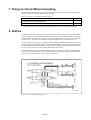
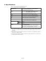
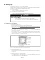
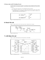
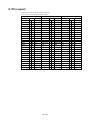
M38C89T-ADF
Temporary Target Board for M38C89RLFS
User's Manual
Rev.1.00
September 1, 2003
REJ10J0296-0100Z
* IC51-1444-1354-18 is a product of Yamaichi Electronics Co., Ltd.
Keep safety first in your circuit designs!
• Renesas Technology Corporation and Renesas Solutions Corporation put the maximum effort into making semiconductor products better
and more reliable, but there is always the possibility that trouble may occur with them. Trouble with semiconductors may lead to personal
injury, fire or property damage. Remember to give due consideration to safety when making your circuit designs, with appropriate
measures such as (i) placement of substitutive, auxiliary circuits, (ii) use of nonflammable material or (iii) prevention against any
malfunction or mishap.
Notes regarding these materials
• These materials are intended as a reference to assist our customers in the selection of the Renesas Technology product best suited to
the customer's application; they do not convey any license under any intellectual property rights, or any other rights, belonging to Renesas
Technology Corporation, Renesas Solutions Corporation or a third party.
• Renesas Technology Corporation and Renesas Solutions Corporation assume no responsibility for any damage, or infringement of any
third-party's rights, originating in the use of any product data, diagrams, charts, programs, algorithms, or circuit application examples
contained in these materials.
• All information contained in these materials, including product data, diagrams, charts, programs and algorithms represents information
on products at the time of publication of these materials, and are subject to change by Renesas Technology Corporation and Renesas
Solutions Corporation without notice due to product improvements or other reasons. It is therefore recommended that customers contact
Renesas Technology Corporation, Renesas Solutions Corporation or an authorized Renesas Technology product distributor for the latest
product information before purchasing a product listed herein. The information described here may contain technical inaccuracies or
typographical errors. Renesas Technology Corporation and Renesas Solutions Corporation assume no responsibility for any damage,
liability, or other loss rising from these inaccuracies or errors. Please also pay attention to information published by Renesas Technology
Corporation and Renesas Solutions Corporation by various means, including the Renesas home page (http://www.renesas.com).
• When using any or all of the information contained in these materials, including product data, diagrams, charts, programs, and algorithms,
please be sure to evaluate all information as a total system before making a final decision on the applicability of the information and
products. Renesas Technology Corporation and Renesas Solutions Corporation assume no responsibility for any damage, liability or
other loss resulting from the information contained herein.
• Renesas Technology semiconductors are not designed or manufactured for use in a device or system that is used under circumstances
in which human life is potentially at stake. Please contact Renesas Technology Corporation, Renesas Solutions Corporation or an
authorized Renesas Technology product distributor when considering the use of a product contained herein for any specific purposes,
such as apparatus or systems for transportation, vehicular, medical, aerospace, nuclear, or undersea repeater use.
• The prior written approval of Renesas Technology Corporation and Renesas Solutions Corporation is necessary to reprint or reproduce
in whole or in part these materials.
• If these products or technologies are subject to the Japanese export control restrictions, they must be exported under a license from the
Japanese government and cannot be imported into a country other than the approved destination. Any diversion or reexport contrary to
the export control laws and regulations of Japan and/or the country of destination is prohibited.
• Please contact Renesas Technology Corporation or Renesas Solutions Corporation for further details on these materials or the products
contained therein.
Precautions to be taken when using this product
• This product is a development supporting unit for use in your program development and evaluation stages. In mass-producing your
program you have finished developing, be sure to make a judgment on your own risk that it can be put to practical use by performing
integration test, evaluation, or some experiment else.
• In no event shall Renesas Solutions Corporation be liable for any consequence arising from the use of this product.
• Renesas Solutions Corporation strives to renovate or provide a workaround for product malfunction at some charge or without charge.
However, this does not necessarily mean that Renesas Solutions Corporation guarantees the renovation or the provision under any
circumstances.
• This product has been developed by assuming its use for program development and evaluation in laboratories. Therefore, it does not fall
under the application of Electrical Appliance and Material Safety Law and protection against electromagnetic interference when used in
Japan.
For inquiries about the contents of this document or product, fill in the text file the installer of the emulator debugger generates in the
following directory and email to your local distributor.
\SUPPORT\Product-name\SUPPORT.TXT
Renesas Tools Homepage http://www.renesas.com/en/tools
( 2 / 14 )
Contents
1. Things to Check When Unpacking ..................................................................................... 4
2. Outline ................................................................................................................................ 4
3. Specifications ..................................................................................................................... 5
4. Setting Up ........................................................................................................................... 6
4.1 Connecting to the Emulator .................................................................................. 6
4.2 Mounting the M38C89MF-xxxFP/M38C89EFFP ................................................ 8
5. Oscillator Circuit ................................................................................................................ 9
5.1 Main Clock Generator Circuit ............................................................................... 9
5.2 Sub Clock Generator Circuit ................................................................................. 9
5.3 How to Use the RC Oscillator Circuit ................................................................. 10
6. Reset Circuit ..................................................................................................................... 10
7. LCD Bias Circuit .............................................................................................................. 10
8. Pin Layout ........................................................................................................................ 11
( 3 / 14 )
1. Things to Check When Unpacking
The M38C89T-ADF package consists of the following products. When unpacking your package,
check to see that all of these components are included.
Table 1.1 Contents of the M38C89T-ADF package
Item
Quantity
M38C89T-ADF temporary target board
1
M38C89T-ADF User's Manual (this manual)
1
* If you find any item missing or faulty, or any suggestion, contact your local distributor.
2. Outline
The M38C89T-ADF is a temporary target board used to develop software with a PC4701 emulator
system. It supplies to the M38C89RLFS MCU the minimum required signals needed to operate the
emulator MCU, including power supply voltage, clock signals and reset signals. Use it when the
target system is not ready. A block diagram of the M38C89T-ADF is shown in Figure 2.1.
IC1 has a pattern for mounting a socket for an M38C89MF-xxxFP/M38C89EFFP. This makes it
possible for this board to debug programs using an emulator MCU in IC2 or execute programs using
an M38C89MF-xxxFP/M38C89EFFP. A socket for M38C89MF-xxxFP/M38C89EFFP and parts
for an LCD bias circuitry are not mounted. Mount them as necessary.
Expansion boards can be installed in the through-holes of connectors J2, J3 and J4. Spacing between
connectors is given in Figure 2.1. Keep connector location in mind when making expansion boards.
Use 2.54-mm-pitch connectors. For pin array, see Table 8.1.
Unit: mm
Figure 2.1 Block diagram and pin layout
( 4 / 14 )
3. Specifications
Table 3.1 lists specifications of the M38C89T-ADF.
Table 3.1 Specifications of the M38C89T-ADF
Applicable MCUs
IC1: 38C8 Group (M38C89MF-xxxFP/M38C89EFFP)
IC2: M38C89RLFS (Emulator MCU)
Clock
Main clock: 4.0MHz oscillator mounted (for IC2 only)
(RC oscillation: approx. 2 MHz*1)
Sub clock: 32.768 kHz mounted (for IC2 only)
VccM
Power supply for IC1 and IC2 (supplied separately*2)
VccU
Power supply for universal part (supplied separately*2)
Vss
Common signal ground (supplied separately*2)
RESET
• Reset circuit mounted (power-on reset and reset switch)
• Connects the reset output of an emulation pod
External dimensions
Others
Width
220 mm
Depth
160 mm
• Universal part prepared
• Through hole for 2.54-mm-pitch connector prepared
• RC oscillator circuit can be selected as a main clock oscillator*3
• Bias circuit for LCD prepared (parts not mounted)
*1 RC oscillation frequency will vary according to MCU power supply voltage, resistance,
temperature, etc. That listed herein was measured for reference purposes only and is not
guaranteed.
*2 Power cannot be supplied from the emulation pod for PC4701 (e.g. M38000TL2-FPD). A
separate power supply is needed.
*3 Jumpers must be changed to enable RC oscillation. For more information, see "5.3 How to Use
the RC Oscillator Circuit" (page 10).
( 5 / 14 )
4. Setting Up
This chapter describes how to set up the M38C89T-ADF.
With this product, the debugging with an emulator MCU and M38C89MF-xxxFP/M38C89EFFP is
possible. Use the M38C89T-ADF mounting one of these MCUs.
To use an emulator MCU:
Read "4.1 Connecting to the Emulator" (this page)
To use the M38C89MF-xxxFP/M38C89EFFP:
Read "4.2 Mounting the M38C89MF-xxxFP/M38C89EFFP" (page 8)
CAUTION
Note on Setting Up:
• Always shut OFF power before connecting the M38C89T-ADF.
• Do not mount the IC1 and IC2 at the same time. Mount either of them only.
4.1 Connecting to the Emulator
(1) Mounting the emulator MCU
Mount the emulator MCU in the IC2 socket on the M38C89T-ADF.
Raise the socket's clamp and insert the emulator MCU flush against the socket's left and bottom
sides, placing the "•" marking on the emulator MCU at the right bottom corner. Then, lower the
clamp to lock the emulator MCU in place.
If your emulator MCU does not have the "•" marking on it, use one pin (back of the MCU) for
positioning as shown below.
MCUs have 20 x 20 pins to the socket's 21 x 21 holes. Since there are more socket holes to MCU
pins, insert the MCU flush against the socket's left and bottom sides. The socket is taped to prevent
improper MCU mounting. Do not peel off the tape.
Figure 4.1 Mounting the emulator MCU on the M38C89T-ADF
(2) Connecting the emulation probe
Insert the connector on the tip of the emulation pod probe to the J1 of this board. For the direction,
see Figure 4.2.
(3) Setting the emulation pod (M38000TL2-FPD)
As the applicable emulator MCU (M38C89RLFS) for this product is RLFS type, set the switch
on the side of the emulation pod to RLSS/RLFS side.
( 6 / 14 )
(4) Connecting the control signal lines
Connect the three lines of the emulation pod to the test pins.
VCC cable (yellow) ........... VccM (test pin with a yellow bead)
GND cable (black) ............. GND (test pin with a black bead)
Reset cable (white) ............. RESET (test pin with a white bead)
Figure 4.2 Connecting the M38C89T-ADF
(5) Setting jumpers
Set the jumpers (JP3 to JP7) according to your application. Table 4.1 describes the functions of
the jumpers for the emulator MCU (IC2).
Table 4.1 Functions of the jumpers (JP) of the M38C89T-ADF (1/2)
Name
Applicable signal
Function
Factory-setting
JP3
Vss (NC)-VLIN
Remain Open.
Open
JP4
OSCSEL
Switches the OSCSEL pin
• Short-circuit: OSCSEL = "L"
Selects the oscillation by ceramic resonator.
• Open: OSCSEL = "H"
Selects the RC oscillation.
Short-circuit
JP5
XIN
R10 side: RC oscillation, X2 side: Oscillation by X2
X2 side
JP6
XOUT
JP7
VccM-VccU
For short-circuit of VccM-VccU
Open
(6) Connecting a power supply
Connect a power supply (not included) to the board's VccM power supply test (large) pin and
GND. Power is supplied to Vcc of IC1 and IC2.
To use the VccU universal power supply, connect a power supply (not included) to the VccU
power supply test pin.
VccM and VccU are not connected on the board. They can be connected by short-circuiting
jumper JP7.
( 7 / 14 )
4.2 Mounting the M38C89MF-xxxFP/M38C89EFFP
(1) Mounting parts
Mount the socket for IC1 and the oscillator circuit part. Table 4.2 lists the applicable parts for this
board.
Table 4.2 Socket for the M38C89MF-xxxFP/M38C89EFFP and applicable oscillator circuit
No.
Part No.
Type name
Remarks
Manufacturer
1
IC1
IC51-1444-1354-18 Yamaichi Electronics Co., Ltd.
144-pin socket
2
X1
CST4.00MGW040 Murata Manufacturing Co., Ltd.
Built-in capacitor type, 4 MHz
3
XC1
SP-T2B 32.768 kHz Seiko Instruments Inc.
On-board type
4
C5, C6
RPE132CH100J50 Murata Manufacturing Co., Ltd.
10 pF
5
R2
6
R3
-
-
RD16S 6.8MΩJ
0 Ω, short-circuit
6.8 MΩ
KOA
(2) Mounting the M38C89MF-xxxFP/M38C89EFFP
To mount the M38C89MF-xxxFP/M38C89EFFP, remove the emulator MCU and install the
M38C89MF-xxxFP/M38C89EFFP in the IC1 socket. Align pin No. 1 with the printed mark.
(3) Setting jumpers (JP)
Set the jumpers (J1 to J4 and J7) according to your applications. Table 4.3 describes the functions
of the jumpers.
Table 4.3 Functions of the jumpers (JP) of the M38C89T-ADF (2/2)
Name
Applicable signal
JP1
XIN
JP2
XOUT
JP3
Function
Factory-setting
R1 side: RC oscillation, X1 side: Oscillation by X1
Open
Vss (NC)-VLIN
Remain Open.
Open
JP4
OSCSEL
Switches the OSCSEL pin
• Short-circuit: OSCSEL = "L"
Selects the oscillation by ceramic resonator
• Open: OSCSEL = "H"
Selects the RC oscillation
Short-circuit
JP7
VccM-VccU
For short-circuit of VccM-VccU
Open
(4) Connecting a power supply
Connect a power supply (not included) to the board's VccM power supply test (large) pin and
GND. Power is supplied to Vcc of IC1 and IC2.
To use the VccU universal power supply, connect a power supply (not included) to the VccU
power supply test pin.
VccM and VccU are not connected on the board. They can be connected by short-circuiting
jumper JP7.
( 8 / 14 )
5. Oscillator Circuit
5.1 Main Clock Generator Circuit
The main clock of 4.0 MHz is mounted (X2 only). Figure 5.1 shows the main clock generator circuit.
Figure 5.1 Main clock generator circuit
5.2 Sub Clock Generator Circuit
The sub clock generator circuit is shown in Figure 5.2. The sub clock oscillates at 32.768 kHz.
Capacitors C19 and C20 have a capacitance of 10 pF, while resistor R11 has a resistance of 0 Ω and
resistor R12 a resistance of 6.8 MΩ. Components are not mounted on the IC1 side.
If MCU power supply voltage is low, it will take time for sub clock oscillation to stabilize. Be aware
of this when changing from the main clock to the sub clock.
Figure 5.2 Sub clock generator circuit
( 9 / 14 )
5.3 How to Use the RC Oscillator Circuit
The clock selection circuit is shown in Figure 5.3. Oscillation can be switched between RC oscillation
and the oscillator by changing the jumpers. The following procedure explains how to switch to RC
oscillation.
(1) Cut jumper JP4. (When JP4 is cut, the OSCSEL pin becomes high.)
(2) To enable RC oscillation in IC1, set resistor R1 (see Table 4.3) in jumpers JP1 and JP2
described in Figure 5.1. To enable RC oscillation in IC2, set resistor R10 (see Table 4.1) in
jumpers JP5 and JP6 described in Figure 5.1.
Figure 5.3 Clock selection circuit
6. Reset Circuit
Figure 6.1 shows the reset circuit. The reset circuit is common for IC1 and IC2.
Figure 6.1 Reset circuit
7. LCD Bias Circuit
Figure 7.1 shows the LCD bias circuit. The parts are not mounted.
Figure 7.1 LCD bias circuit
( 10 / 14 )
8. Pin Layout
Table 8.1 lists the pin layout of the connectors.
Table 8.1 Pin layout of the M38C89T-ADF
J2
Signal
J3
Pin No.
Signal
Signal
J4
Pin No.
Signal
Signal
Signal
Pin No.
VccM
1
2
GND
1
2
GND
VccM
1
2
GND
SEG0/COM16
3
4
SEG1/COM17 SEG46
3
4
SEG47
P00
3
4
P01
SEG2/COM18
5
6
SEG3/COM19 SEG48
5
6
SEG49
P02
5
6
P03
SEG4/COM20
7
8
SEG5/COM21 SEG50
7
8
SEG51
P04
7
8
P05
SEG6/COM22
9
10 SEG7/COM23 SEG52
9
10 SEG53
P06
9
10 P07
SEG8
11
12 SEG9
SEG54
11
12 SEG55
P10
11
12 P11
SEG10
13
14 SEG11
SEG56
13
14 SEG57
P12
13
14 P13
SEG12
15
16 SEG13
SEG58
15
16 SEG59
P14
15
16 P15
SEG14
17
18 SEG15
SEG60/COM31 17
18 SEG61/COM30 P16
17
18 P17
SEG16
19
20 SEG17
SEG62/COM29 19
20 SEG63/COM28 P20
19
20 P21
SEG18
21
22 SEG19
SEG64/COM27 21
22 SEG65/COM26 P22
21
22 P23
SEG20
23
24 SEG21
SEG66/COM25 23
24 SEG67/COM24 P24
23
24 P25
SEG22
25
26 SEG23
COM0
25
26 COM1
P26
25
26 P27
SEG24
27
28 SEG25
COM2
27
28 COM3
P30
27
28 P31
SEG26
29
30 SEG27
COM4
29
30 COM5
P32
29
30 P33
SEG28
31
32 SEG29
COM6
31
32 COM7
P40
31
32 P41
SEG30
33
34 SEG31
COM8
33
34 COM9
P42
33
34 P43
SEG32
35
36 SEG33
COM10
35
36 COM11
P44
35
36 P45
SEG34
37
38 SEG35
COM12
37
38 COM13
P46
37
38 P47
SEG36
39
40 SEG37
COM14
39
40 COM15
NC
39
40 NC
SEG38
41
42 SEG39
NC
41
42 NC
NC
41
42 NC
SEG40
43
44 SEG41
NC
43
44 NC
NC
43
44 NC
SEG42
45
46 SEG43
NC
45
46 NC
NC
45
46 NC
SEG44
47
48 SEG45
NC
47
48 NC
NC
47
48 NC
GND
49
50 VccU
GND
49
50 VccU
GND
49
50 VccU
VccM
( 11 / 14 )
MEMO
( 12 / 14 )
M38C89T-ADF User's Manual
Rev.1.00
September 1, 2003
REJ10J0296-0100Z
COPYRIGHT ©2003 RENESAS TECHNOLOGY CORPORATION
AND RENESAS SOLUTIONS CORPORATION ALL RIGHTS RESERVED