1
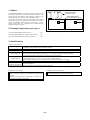
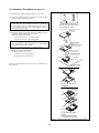
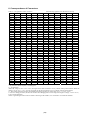
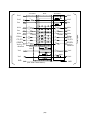
R0E330850ACBP0
Protection Board for M16C/60 Series M16C/62P Group and M32C/80 Series Emulator
User’s Manual
CAUTION
Renesas Tools Homepage
Rev.1.02
Jan. 08, 2008
REJ10J1734-0102
If the requirements shown in the "CAUTION" sentences are ignored,
the equipment may cause personal injury or damage to the products.
http://www.renesas.com/tools
(1/8)
1. Outline
LED1
40b
1b
40a
1a
TOOL SIDE
40
b
40
a
1b
1a
R0E330850ACBP0
protection board
MADE IN JAPAN
Pb Free
The R0E330850ACBP0 is a protection board for the M16C/60
Series M16C/62P Group and M32C/80 Series emulator. This
product protects the emulator from improper connections by
connecting to between the converter board and emulator.
This product is designed to protect the emulator from troubles
caused by applying overvoltage to port pins. Note that it cannot
protect the emulator when applying overvoltage or reverse
voltage to the power pins, or applying more voltage than the
allowable voltage to each pin.
R0E330850ACBP0
User's Manual (Jpn/Eng)
J2
J1
LED2
R0E330850ACBP0 REV.A
RENESAS
RENESAS
R0E330850ACBP0
R0E330850ACBP0
ユーザーズマニュアル
User's Manual
ルネサス テクノロジ
www.renesas.com
2. Package Components (See Figure 1)
(1/*)
Renesas Technology
www.renesas.com
(1/*)
Figure 1 Package components of the R0E330850ACBP0
(1) R0E330850ACBP0 protection board ......................... 1pc.
(2) R0E330850ACBP0 User's Manual (This manual) ..... 1pc.
(2) R0E330850ACBP0 User's Manual (Japanese)........... 1pc.
3. Specifications
Table 1 Specifications
Applicable products
Interface connectors
Vcc
Protect function
Protected pins*
M30830T-EPB, M30850T2-EPB, M30870T-EPB, M30880T-EPB, M3062PT2-EPB,
M30850T3-CPE, M30870T2-CPE, M3062PT3-CPE
80pin 0.8mm pitch (Matsushita Electric Works, Ltd.)
3.0 - 5.5 V (When the power pin Vcc1 is set to 5.6 V or more, LED1 and LED2 light.)
Overvoltage: When applying voltage up to +10 V, the input voltage is limited by a diode.
Reverse voltage: When applying voltage up to -10 V, the input voltage is limited by a diode.
Over current: When the signal is short-circuited, the current is limited.
Signal input/output pins except pins below.
Pins not protected: Vcc1, Vss1, Vcc2, Vss2, AVcc, VREF and AVss
(Note that pins of BYTE, CNVss, P70 and P71 are not protected against overvoltage)
Max.120 mA (without error) *Power is supplied from the Vcc1 pin of the user system
Icc
Insertion/removal
50 times guaranteed
iterations of connector
* About protections of each pin, see “Table 2 Correspondence of the connectors”.
Examples to be protected
- Connection between a port and +10[V] signal
- Short-circuiting between a port and ECL (-5.5[V]) output
signal
- Short-circuiting between output ports or between an
output port and the power supply
Examples NOT to be protected
- Applying +9[V] to the power supply
- Connection between a port and +24[V] signal
(2/9)
4. Connection Procedure (See Figure 2)
J3
J4
1b
1b
40b
1a
1a
40b
(1) Check that neither the RVC12 nor RVS12 on this product
has been disconnected using a tester.
40a
40a
The procedure for connecting this product is shown below.
RVC12
RVS12
- When the RVC12 and RVS12 are disconnected, this
product may have been damaged because of overload. Do
not connect this product with the emulator or user system.
As the emulator may also have been damaged, make a
request for inspection of it.
(1) Check neither RVC12 nor
RVS12 have been disconnected
before using this product.
Emulator
(2) Mount this product on the converter board. Make sure NOT
to use this product without the user system.
Install the connectors as follows.
Converter board CN1 = J3 of this product
Converter board CN2 = J4 of this product
(J4)
(J3)
(3)
- Check to see if power is off.
- Do not attach this product between the PCA7501EPBA
board and the M3T-FLX160-EPB.
- Be sure not to attach the board in a wrong direction.
This product
J2 Side
Match the direction
of the connectors
J1Side
(J4)
(3) Mount the emulator on this product.
Install the connectors as follows.
Emulator J3 = J1 of this product
Emulator J4 = J2 of this product
(J3)
(2)
Match the direction
of the connectors
Converter board
CN2 side
Socket
CN1 side
1pin
Before using this product, be sure to read "5. Precautions" on
the next page.
User system
Do NOT use without the
user system.
M3T-FLX160-EPB
-
-
PCA7501EPBA
Do not attach this product
between
the PCA7501EPBA board
and the M3T-FLX160-EPB.
Figure 2 Connection procedure of the R0E330850ACBP0
(3/9)
5. Precautions
CAUTION
Caution to Be Taken for This Product:
z Be sure to connect this product to the user system, and supply power from the Vcc1 pin.
z Use the power pin Vcc1 with 5.5 V or less. If the Vcc1 pin is set to 5.6 V or more accidentally, the LED1 and LED2
will light up to notify it. If the LEDs light up, turn the power off immediately.
z If the pins protected against overvoltage are overvoltaged, the voltage of the Vcc1 pin may rise up to 5.6 V because
of reverse current. When you need to maintain the Vcc1 pin voltage of the user system, add dummy resistance and
voltage regulator diode to the power line of the Vcc1. (Figure 3 is a mounting example.)
z Do NOT touch this product while powering on. Part of the circuit may be at a high temperature immediately after
turning off the emulator. Please take some time to let it cool down before touching this product.
IMPORTANT
Notes on This Product:
z It does not provide any guarantees to protect the emulator from any possible improper connection with the user
system. For details, refer to the specifications.
z When using this product, the electrical characteristics change slightly compared with when not using it. For final
evaluation or characteristics verification, use the evaluation MCU.
z We cannot accept any request for repair. When requesting for repair of the emulator used with this product, refer to
“7. Troubleshooting” on page 6.
z For inquiries about the product or the contents of this manual, contact your local distributor.
Renesas Tools Homepage
http://www.renesas.com/tools
Figure 3 Example of component mounting (When restricting the voltage to 3.6 V or less in the 3.3 V user system)
(4/8)
6. Correspondence of Connectors
Table 2 Correspondence of the connectors
No.
J3-1a
Signals
Protections
GND
No.
-
J3-1b
(The following signals are for the M32C/87 Group)
Signals
Protections
No.
P86
V+,V-,I
J4-1a
Signals
Protections
GND
No.
-
J4-1b
Signals
RESET#
Protections
V+,V-,I
J3-2a
P87
V+,V-,I
J3-2b
CNVss
XOUT
Vss1 *
V-,I
J3-3b
P140
J4-3a
XIN
V+,V-,I
V+,V-,I
J4-2b
BYTE
V-,I
V+,V-,I
J4-2a
J3-3a
J4-3b
Vcc1 *
J3-4a
P141
V+,V-,I
J3-4b
P142
V+,V-,I
J4-4a
P85
V+,V-,I
J4-4b
P84
V+,V-,I
J3-5a
P143
V+,V-,I
J3-5b
P144
V+,V-,I
J4-5a
P83
V+,V-,I
J4-5b
P82
V+,V-,I
J3-6a
P145
V+,V-,I
J3-6b
P146
V+,V-,I
J4-6a
P81
V+,V-,I
J4-6b
P80
V+,V-,I
J3-7a
P90
V+,V-,I
J3-7b
P91
V+,V-,I
J4-7a
P77
V+,V-,I
J4-7b
P76
V+,V-,I
J3-8a
P92
V+,V-,I
J3-8b
P93
V+,V-,I
J4-8a
P75
V+,V-,I
J4-8b
P74
V+,V-,I
J3-9a
P94
V+,V-,I
J3-9b
P95
V+,V-,I
J4-9a
P73
V+,V-,I
J4-9b
P72
V+,V-,I
J3-10a
P96
V+,V-,I
J3-10b
GND
-
J4-10a
P71
V-,I
J4-10b
GND
J3-11a
GND
-
J3-11b
P97
V+,V-,I
J4-11a
GND
-
J4-11b
P70
J3-12a
AVcc
J3-12b
VREF
V~
J4-12a
P67
V+,V-,I
J4-12b
Vcc1
-
V~
-
V-,I
J3-13a
P100
V+,V-,I
J3-13b
AVss
P66
Vss1
V+,V-,I
J3-14b
P102
J4-14a
P65
V+,V-,I
V+,V-,I
J4-13b
P101
V~
V+,V-,I
J4-13a
J3-14a
J4-14b
P64
V+,V-,I
J3-15a
P103
V+,V-,I
J3-15b
P104
V+,V-,I
J4-15a
P63
V+,V-,I
J4-15b
P62
V+,V-,I
J4-16a
P61
V+,V-,I
J4-16b
P60
V+,V-,I
V+,V-,I
J3-16a
P105
V+,V-,I
J3-16b
P106
V+,V-,I
J3-17a
P107
V+,V-,I
J3-17b
Vcc1
-
J4-17a
P137
V+,V-,I
J4-17b
P136
J3-18a
P150
V+,V-,I
J3-18b
Vss1
-
J4-18a
P135
V+,V-,I
J4-18b
P134
V+,V-,I
J3-19a
P151
V+,V-,I
J3-19b
P152
V+,V-,I
J4-19a
P57
V+,V-,I
J4-19b
P56
V+,V-,I
J3-20a
P153
V+,V-,I
J3-20b
GND
P55
GND
-
J3-21b
P154
J4-21a
GND
V+,V-,I
-
J4-20b
GND
V+,V-,I
J4-20a
J3-21a
J4-21b
P54
V+,V-,I
J3-22a
P155
V+,V-,I
J3-22b
P156
V+,V-,I
J4-22a
P133
V+,V-,I
J4-22b
Vss2
P00
V+,V-,I
P132
V+,V-,I
J4-23b
Vcc2
-
J4-24a
P131
V+,V-,I
J4-24b
P130
V+,V-,I
J4-25a
P53
V+,V-,I
J4-25b
P52
V+,V-,I
P51
V+,V-,I
J4-26b
P50
V+,V-,I
P127
V+,V-,I
J4-27b
P126
V+,V-,I
J4-28b
P47
V+,V-,I
V+,V-,I
J3-23a
P157
V+,V-,I
J3-23b
J4-23a
J3-24a
P01
V+,V-,I
J3-24b
P02
V+,V-,I
J3-25a
P03
V+,V-,I
J3-25b
P110
V+,V-,I
P112
V+,V-,I
P114
V+,V-,I
P05
V+,V-,I
J4-28a
P125
V+,V-,I
V+,V-,I
J4-29a
P46
V+,V-,I
J4-29b
P45
-
J4-30a
P44
V+,V-,I
J4-30b
GND
J3-26a
J3-27a
J3-28a
P111
P113
P04
V+,V-,I
V+,V-,I
V+,V-,I
J3-26b
J3-27b
J3-28b
J4-26a
J4-27a
-
J3-29a
P06
V+,V-,I
J3-29b
P07
J3-30a
P10
V+,V-,I
J3-30b
GND
J3-31a
GND
-
J3-31b
P11
V+,V-,I
J4-31a
GND
-
J4-31b
P43
V+,V-,I
J3-32a
P12
V+,V-,I
J3-32b
P13
V+,V-,I
J4-32a
Vcc2
-
J4-32b
P42
V+,V-,I
J3-33a
P14
V+,V-,I
J3-33b
P15
V+,V-,I
J4-33a
Vss2
-
J4-33b
P41
V+,V-,I
J3-34a
P16
V+,V-,I
J3-34b
P17
V+,V-,I
J4-34a
P40
V+,V-,I
J4-34b
P37
V+,V-,I
J3-35a
P20
V+,V-,I
J3-35b
P21
V+,V-,I
J4-35a
P36
V+,V-,I
J4-35b
P35
V+,V-,I
J3-36a
P22
V+,V-,I
J3-36b
P23
V+,V-,I
J4-36a
P34
V+,V-,I
J4-36b
P33
V+,V-,I
J3-37a
P24
V+,V-,I
J3-37b
P25
V+,V-,I
J4-37a
P32
V+,V-,I
J4-37b
P31
V+,V-,I
J3-38a
P26
V+,V-,I
J3-38b
P27
V+,V-,I
J4-38a
P124
V+,V-,I
J4-38b
P123
V+,V-,I
J3-39a
Vss2
-
J3-39b
P30
V+,V-,I
J4-39a
P122
V+,V-,I
J4-39b
P121
V+,V-,I
J3-40a
Vcc2
-
J3-40b
GND
-
J4-40a
P120
V+,V-,I
J4-40b
GND
-
-
Notes:
-: No protection (direct-coupled), *: Feeding point
V~: No protection
(When the voltage is set to -1.0 V or less, the signal will be short-circuited to Vss by a diode on the protection board. When the
voltage is set to “Vcc1 + 1.0” V or more, the signal will be short-circuited to Vcc1 by a diode on the protection board.)
V+: Overvoltage protection (Protects the emulator from being applied overvoltage from “Vcc1 + 1.0” V to +10 V.)
V-: Reverse voltage protection (Protects the emulator from being applied reverse voltage from negative voltage -1.0 V to -10 V.)
I: Over current protection
GND is a ground signal of the connector. When connecting to the emulator, it is connected to Vss inside the emulator.
(5/8)
7. Troubleshooting
If you have trouble when using this product with connected to the emulator, refer to the following procedures.
Table 3
Type
Improper
use
Items to check when having trouble with this product used
Problems
Items to check
Used without the user system.
After turning off the power, verify that this product is connected to the user system, and
then use it.
Installed on a wrong position.
Applied more than 5.5[V] voltage
or reverse voltage to the power
pin Vcc1/Vss1.
Applied more than 10[V] of
voltage or more than -10[V] of
reverse voltage to each pin other
than the power pins.
Error
Error was detected by
self-check of the emulator.
the
product
Check to see if this product is disconnected to the emulator. When the product is
connected to the emulator, after turning off the power and disconnecting it, execute the
self-check of the emulator again.
See the chapter of the Self-check in the user’s manual of the emulator.
The self-check needs to be performed with the emulator disconnected from the
product.
It indicates that abnormal voltage is being supplied. Turn the power off immediately
and disconnect this product and the emulator. Check the connection between the
emulator and the user system, the power supply voltage, and inadequateness or
misuse of the user system.
LED of this product lights up.
FUSE of this
disconnected.
This product and the emulator may have been damaged due to improper use of this
product. Turn the power off immediately and disconnect this product and the emulator.
Make a request for support or repair according to the procedure shown in Figure 4.
Add the detailed information about the improper use to the column of Cause of fault in
the Repair Request Sheet.
is
This product is damaged due to the overload that exceeded the allowable limit of this
product. The emulator may also have been damaged. Make a request for support or
repair according to the procedure shown in Figure 4.
When requesting for support or repair, please inform us of this product being used. If you request repair for the emulator used with
this product, send us both the emulator and this product (We cannot accept any request for repair of this product).
Support /repair request
Was this product
connected to the
emulator?
Unconnected
See the Emulator’s user’s
manual to request for
support/repair.
Connected
Disconnect this product and the
user system from the emulator and
execute the self-check of the
emulator.
Complete
Check t o s e e if the FUSE of this
product is disconnected.
Make a request for support or repair. Be sure to inform us of this product being
used with the emulator, and add the following information of (1)(2) to the column
of Operating environment on the Repair Request Sheet, and that of (3)(4) to the
column of Symptoms.
(1) [Optional product : R0E330850ACBP0]
(2) [Serial number: (Rot number of R0E330850ACBP0)]
(3) [Results of the self-check : (LED status or the error massage)]
(4) [FUSE status of R0E330850ACBP0:
(Normal, RVC12 disconnected or RVS12 disconnected)]
Complete
Figure 4
Note: If you request repair for the emulator used
with this product, send us both the emulator and
this product.
Support/repair request flow when using this product
(6/8)
8. Appendix
Table 4 Correspondence of part numbers and signals
Signals
J1J2side resistors
Diode
J3J4 side resistors
CNVss
BYTE
RESET#
XIN
XOUT
P00-P07
P10-P17
P20-P27
P30-P37
P40-P47
P50-P57
P60-P67
P70,P71
P72-P67
P80-P85
P86
P87
P90-P97
P100-P103
P105-P107
P104
P110-P114
P120-P127
P130-P137
P140-P146
P150-P157
AVcc
VREF
AVss
Vcc1
RCNV1
RBYT1
RRES1
RXIN1
RXO1
N6,N17
N3,N10
N1,N7
N5,N8,R3
N11,N15
N12,N20
N23,N26
N29
N29,N31
N28,N33
R11
R12
N25,N30
(DCNV1), D87
(DBYT1), D94
DRES1
DXIN1
DXO1
D10,D13,D21,D56,D68,D73
D1,D7,D14,D49,D55,D59
D2,D8,D46,D47,D48,D51
D6,D30,D43,D53,D54
D15,D19,D23,D58,D61,D65
D12,D20,D24,D52,D57,D66
D28,D31,D69,D78.D82,D74
(D86), D36,D89
D36,D37,D42,D89,D92
D35,D41,D83,D93
D94
D87
D30,D38,D79,D80,D88,D95
RCNV2
RBYT2
RRES2
RXIN2
RXO2
N42,N50
N38,N45
N35,N41
N36,N40,R15
N44,N48
N43,N51
N54,N57
N60
N60,N63
N61,N66
R18
R17
N58,N64
N21,N24
D26,D29,D32,D34,D72,D76,D85,D91
N56,N59
R10
N13,N14
N2,N4,N9
N16,N22
N27,N32
N18,N19
RAVC1
RVRF1
RAVS1
RVC2
-
D34
D17,D18,D62,D63
D4,D5,D9,D44,D45,D50
D16,D27,D60,D64,D70,D75
D33,D39,D40,D84,D90
D25,D67,D71,D77,D81
DAVC1
D32,D91
D32,D91
-
R16
N46,N49
N34,N37,N39
N47,N55
N62,N65
N52,N53
RAVC2
RVRF2
RAVS2
RVC12
RVC10
(RVC11)
RVS12
-
Vcc2
Vss
Notes) - : No mount position, (…): Unmount
(7/8)
Remark
DCNV1 unmount
DBYT1 unmount
D86 unmount
0ohm
0ohm
0ohm
See Figure 5
See Figure 5
See Figure 5
0ohm
See Figure 5
See Figure 5
J1J2 side R
Vcc1
Diode
J3J4 side R
J2-3b
J4-3b
0.5A Fuse
RVC12
0
Vcc2
Vss
RVC2
J4-2b
0.5A Fuse
J2-2b
Vcc1
Vcc2
Vss
RVS12
RAVC1
To emulator
CNVss
RVRF1
J1-12b
RAVS1
P70,P71
RESET#,
X IN,X OUT
otherPort
Vcc1
0
0
J1-13b
22
22
22
22
22
22
Power
block
AVcc
RAVC2
J3-12a
RVRF2
J3-12b
RAVS2
J3-13b
0
0
V REF
AVss
0
0
J1-12a
V REF
AVss
CNVss
BYTE
P70,P71
RESET#,
X IN ,X OUT
otherPort
UDZS5.6B
ZD6
110
0
RVC10
J1-17b
ZD3
CV3
Vcc1
ZD5
CV5
GND
0
RVC11
J3-17b
Vcc1
Vcc1
GND
(Note: Diode is Rohm RB731U)
Figure 5 Connection diagram
(8/8)
To user system
AVcc