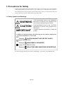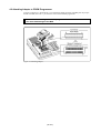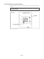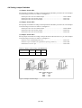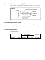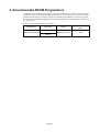
1
PCA7438FF-100
Flash memory programming adapter for 38000 Series
User's Manual
Rev.1.00
September 1, 2003
REJ10J0251-0100Z
* R4945 and R4945A are trademarks of Advantest Corporation.
Keep safety first in your circuit designs!
• Renesas Technology Corporation and Renesas Solutions Corporation put the maximum effort into making semiconductor products better
and more reliable, but there is always the possibility that trouble may occur with them. Trouble with semiconductors may lead to personal
injury, fire or property damage. Remember to give due consideration to safety when making your circuit designs, with appropriate
measures such as (i) placement of substitutive, auxiliary circuits, (ii) use of nonflammable material or (iii) prevention against any
malfunction or mishap.
Notes regarding these materials
• These materials are intended as a reference to assist our customers in the selection of the Renesas Technology product best suited to
the customer's application; they do not convey any license under any intellectual property rights, or any other rights, belonging to Renesas
Technology Corporation, Renesas Solutions Corporation or a third party.
• Renesas Technology Corporation and Renesas Solutions Corporation assume no responsibility for any damage, or infringement of any
third-party's rights, originating in the use of any product data, diagrams, charts, programs, algorithms, or circuit application examples
contained in these materials.
• All information contained in these materials, including product data, diagrams, charts, programs and algorithms represents information
on products at the time of publication of these materials, and are subject to change by Renesas Technology Corporation and Renesas
Solutions Corporation without notice due to product improvements or other reasons. It is therefore recommended that customers contact
Renesas Technology Corporation, Renesas Solutions Corporation or an authorized Renesas Technology product distributor for the latest
product information before purchasing a product listed herein. The information described here may contain technical inaccuracies or
typographical errors. Renesas Technology Corporation and Renesas Solutions Corporation assume no responsibility for any damage,
liability, or other loss rising from these inaccuracies or errors. Please also pay attention to information published by Renesas Technology
Corporation and Renesas Solutions Corporation by various means, including the Renesas home page (http://www.renesas.com).
• When using any or all of the information contained in these materials, including product data, diagrams, charts, programs, and algorithms,
please be sure to evaluate all information as a total system before making a final decision on the applicability of the information and
products. Renesas Technology Corporation and Renesas Solutions Corporation assume no responsibility for any damage, liability or
other loss resulting from the information contained herein.
• Renesas Technology semiconductors are not designed or manufactured for use in a device or system that is used under circumstances
in which human life is potentially at stake. Please contact Renesas Technology Corporation, Renesas Solutions Corporation or an
authorized Renesas Technology product distributor when considering the use of a product contained herein for any specific purposes,
such as apparatus or systems for transportation, vehicular, medical, aerospace, nuclear, or undersea repeater use.
• The prior written approval of Renesas Technology Corporation and Renesas Solutions Corporation is necessary to reprint or reproduce
in whole or in part these materials.
• If these products or technologies are subject to the Japanese export control restrictions, they must be exported under a license from the
Japanese government and cannot be imported into a country other than the approved destination. Any diversion or reexport contrary to
the export control laws and regulations of Japan and/or the country of destination is prohibited.
• Please contact Renesas Technology Corporation or Renesas Solutions Corporation for further details on these materials or the products
contained therein.
Precautions to be taken when using this product
• This product is a development supporting unit for use in your program development and evaluation stages. In mass-producing your
program you have finished developing, be sure to make a judgment on your own risk that it can be put to practical use by performing
integration test, evaluation, or some experiment else.
• In no event shall Renesas Solutions Corporation be liable for any consequence arising from the use of this product.
• Renesas Solutions Corporation strives to renovate or provide a workaround for product malfunction at some charge or without charge.
However, this does not necessarily mean that Renesas Solutions Corporation guarantees the renovation or the provision under any
circumstances.
• This product has been developed by assuming its use for program development and evaluation in laboratories. Therefore, it does not fall
under the application of Electrical Appliance and Material Safety Law and protection against electromagnetic interference when used in
Japan.
Renesas Tools Homepage http://www.renesas.com/en/tools
( 2 / 18 )
Contents
1. Precautions for Safety ......................................................................................................... 4
1.1 Safety Symbols and Meanings .............................................................................. 4
2. Introduction ........................................................................................................................ 6
2.1 Things to Check When Unpacking ....................................................................... 6
3. Specifications ..................................................................................................................... 7
4. How to Write the Program ................................................................................................. 8
4.1 Programming Procedures ...................................................................................... 8
4.2 Attaching Adapter to PROM Programmer ............................................................ 9
4.3 Inserting MCU into Programming Adapter ........................................................ 10
4.4 Setting Jumper Switches ..................................................................................... 11
4.5 Precautions When Opening and Closing IC Socket ............................................ 12
4.6 Precautions When Handling Adapter .................................................................. 12
4.7 Setting Programming Area .................................................................................. 12
5. Recommended PROM Programmers ............................................................................... 13
6. Memory Maps .................................................................................................................. 14
7. Troubleshooting ................................................................................................................ 15
7.1 Errors That Occur When Writing to ROM ......................................................... 15
7.1.1 When Newly Purchased ........................................................................ 15
7.1.2 Previously Written Normally ................................................................ 15
7.2 MCU Does Not Function Normally .................................................................... 16
7.3 Other Precautions ................................................................................................ 16
7.3.1 About the Recommended PROM Programmer .................................... 16
7.3.2 About Reading Out of Device Identification Code .............................. 16
7.4 How to Request for Support ................................................................................ 16
To use the product properly
Precautions for Safety
• In both this User's Manual and on the product itself, several icons are used to insure
proper handling of this product and also to prevent injuries to you or other persons,
or damage to your properties.
• The icons' graphic images and meanings are given in "Chapter 1. Precautions for
Safety". Be sure to read this chapter before using the product.
( 3 / 18 )
1. Precautions for Safety
In both the user's manual and on the product itself, several icons are used to insure proper handling
of this product and also to prevent injuries to you or other persons, or damage to your properties.
This chapter describes the precautions which should be taken in order to use this product safely and
properly. Be sure to read this chapter before using this product.
1.1 Safety Symbols and Meanings
WARNING
If the requirements shown in the "WARNING"
sentences are ignored, the equipment may
cause serious personal injury or death.
CAUTION
If the requirements shown in the "CAUTION"
sentences are ignored, the equipment may
malfunction.
IMPORTANT
It means important information on using this
product.
In addition to the three above, the following are also used as appropriate.
means WARNING or CAUTION.
Example:
CAUTION AGAINST AN ELECTRIC SHOCK
means PROHIBITION.
Example:
DISASSEMBLY PROHIBITED
means A FORCIBLE ACTION.
Example:
UNPLUG THE POWER CABLE FROM THE RECEPTACLE.
The following pages describe the symbols "WARNING", "CAUTION", and "IMPORTANT".
( 4 / 18 )
WARNING
Warning for Use Environment:
• This equipment is to be used in an environment with a maximum ambient temperature of 35˚C. Care
should be taken that this temperature is not exceeded.
• Select the proper programming mode of the PROM programmer.
CAUTION
Cautions to Be Taken for This Product:
• Do not disassemble or modify this product. Disassembling or modifying this product can cause
damage.
• Use caution when handling this product. Be careful not to apply a mechanical shock such as falling.
• Do not directly touch the connector pins of this product.
• Be careful with the static electricity when handling this product and the MCU.
When Not Using This Product for a Long Time:
(1) Attach the connector pins of this product to the conductive sponge.
(2) Put it into a conductive polyvinyl, and keep it in the package case shipped from the factory.
(3) Store it in the place where humidity and temperature are low and direct sunshine does not strike.
IMPORTANT
When Using The Product:
• Attach this product to the IC socket on the PROM programmer properly.
• Insert the MCU to the IC socket of this product properly.
• When opening and closing the IC socket of this product, be sure to keep it horizontal.
• Be sure to set the programming area as described in this user's manual.
• Do not use the PROM programmer's device identification code readout function.
( 5 / 18 )
2. Introduction
This product is a flash memory programming adapter for Renesas 38000 Series of 8-bit microcomputers. The adapter is a tool that can be used to write programs into internal flash memory of
microcomputers using a commercially available PROM programmer.
This manual describes the specifications and the operation.
Figure 2.1 shows the external view and constituent parts of the adapter.
Figure 2.1 External view and constituent parts
2.1 Things to Check When Unpacking
This product consists of the items listed in Table 2.1. Check to see that it contains all of the items.
Table 2.1 Package components
Main unit
PCA7438FF-100
Interface unit
PCA7438B
Connector
PCA7402E (32 pins)
User's manual
This manual
If any part is missing or there is any doubt about your product package, contact your local distributor.
( 6 / 18 )
3. Specifications
Table 3.1 lists specifications of the programming adapter.
Table 3.1 Specifications of the programming adapter
Applicable MCU
M38B79FFFP (100-pin 0.65mm-pitch QFP)
1MHz
(Supplied by the ceramic oscillator mounted on the adapter)
Operating clock frequency
Power supply
Supplied from Vcc of the PROM programmer
IC socket
IC51-1004-814-6 (made by Yamaichi Electronics Co., Ltd.)
Board to insert a programmable MCU
(IC socket mounted on it)
Main unit
Board
configuration
PCA7438B
(Interface unit)
PCA7402E
(Connector)
( 7 / 18 )
Interface board
(Connected by two rows of standard-pitch 18-pin
connectors and two rows of standard-pitch 16-pin
connectors to the upper and lower boards)
Board to connect to the PROM programmer
(Standard-pitch 32-pin pin-header mounted)
4. How to Write the Program
This chapter describes how to write programs using a PROM programmer. For details on how to
operate the PROM programmer, refer to the user's manual of the PROM programmer.
4.1 Programming Procedures
Follow procedures (1) to (8) to write programs into the MCU.
(1) Read the program into the PROM programmer.
(2) Attach the adapter to the PROM programmer. (see section 4.2)
(3) Set the jumper switches (SW1, SW2 and SW3). (see section 4.4)
(4) Insert the MCU into the adapter. (see section 4.3)
(5) Specify the programming area of the MCU using the PROM programmer. (see section 4.7) *1
(6) Using the PROM programmer's erase check function, check whether data can be written into
the programming area of the MCU. *2
(7) Write the program into the programming area of the MCU using the PROM programmer. *2
(8) Verify the programming area of the MCU using the PROM programmer to check whether the
program is written into the MCU correctly. *2
*1 Be sure to set the programming area. Otherwise the mode's shift to the programming mode may not be
performed successfully. The erase check function etc. may not also be performed completely.
*2 Some PROM programmers perform the steps (6) through (8) automatically.
( 8 / 18 )
4.2 Attaching Adapter to PROM Programmer
As shown in Figure 4.1, attach the No. 1 pin of the PCA7402E connector (standard-pitch 32-pin pinheader mounted) to the No. 1 pin of the IC socket of the PROM programmer.
Be careful when attaching to the PROM programmer because incorrect insertion
can cause fatal damage to the MCU.
Figure 4.1 Attaching adapter
( 9 / 18 )
4.3 Inserting MCU into Programming Adapter
As shown in Figure 4.2, insert the No. 1 pin of the MCU into the No. 1 pin of the IC socket on the
main unit.
Be careful when inserting the MCU because incorrect insertion can cause fatal
damage to the MCU.
Top view
Figure 4.2 Inserting MCU
( 10 / 18 )
4.4 Setting Jumper Switches
(1) Jumper Switch SW1
Set the jumper switch SW1 according to the output format of the MCU ports P20 to P23. The examples
of switch settings are shown in Table 4.1 and Figure 4.3.
• When ports P20 to P23 are CMOS output ........................................................ SW1: CMOS
• When ports P20 to P23 are Pch output .............................................................. SW1: Pch
• When ports P20 to P23 are Nch output .............................................................SW1: Nch
(2) Jumper Switch SW2
Set the jumper switch SW2 according to the output format of the MCU ports P24 to P27. The examples
of switch settings are shown in Table 4.1 and Figure 4.3.
• When ports P24 to P27 are CMOS output ........................................................ SW2: CMOS
• When ports P24 to P27 are Pch output .............................................................. SW2: Pch
• When ports P24 to P27 are Nch output .............................................................SW2: Nch
(3) Jumper Switch SW3
Set the jumper switch SW3 according to the specification of the sub-clock XCIN pin. The examples
of switch settings are shown in Table 4.1 and Figure 4.3.
• When XCIN pin is dedicated pin for XCIN ..........................................................SW3: ON
• When XCIN pin is used also as a general I/O port (e.g. P80/XCIN) .................... SW3: OFF
• When there is no XCIN pin ................................................................................ SW3: OFF
Table 4.1 Jumper switch settings of M38B79FFFP
MCU
SW1
SW2
SW3
M38B79FFFP
Pch
Pch
OFF
Note: Switch settings for
SW1 ....... Pch
SW2 ....... Pch
SW3 ....... ON
Figure 4.3 Jumper switch settings
( 11 / 18 )
4.5 Precautions When Opening and Closing IC Socket
When opening and closing the IC socket, hold the adapter horizontally as shown in Figure 4.4.
Otherwise the inside of the IC socket may become damaged and cause an electrical insulation failure.
Side view
Figure 4.4 Holding the adapter in a horizontal position
4.6 Precautions When Handling Adapter
Do not directly touch the connector in the IC socket and the pins on the PROM programmer connector
because dirt may cause an electrical insulation failure.
When not using this product, attach the connector pins of this product to the conductive sponge as
it was shipped from the factory.
4.7 Setting Programming Area
When writing and erasing programs, be sure to set the programming area. And also, specify its device
of the PROM programmer.
Table 4.1 Programming area
PROM programmer
MCU
M38B79FFFP
Device
Programming area
Internal flash
memory
area of MCU
M5M28F101
0100016 - 0FFFF16
100016 - FFFF16
ROM size
60KB
( 12 / 18 )
5. Recommended PROM Programmers
The PROM programmers listed in Table 5.1 are recommended for this product. Using the actual
products, we have verified that these PROM programmers can be used to write programs without
problem. Nonconformity occurring by using any other PROM programmers can not be supported.
For the latest type of PROM programmers, contact the manufacturer to confirm whether it can be used
for your product.
Table 5.1 Recommended PROM programmers
Manufacturer
Type name
Device
Programming voltage
(Vpp)
M5M28F101 mode
12.0V
R4945
Advantest Corporation
R4945A
( 13 / 18 )
6. Memory Maps
Figure 6.1 shows memory maps of the MCU and the PROM programmer.
000016
0000016
0FFF16
100016
00FFF16
0100016
Internal flash
memory area
(60K bytes)
Programming area
0FFFF16
1000016
FFFF16
1FFFF16
MCU
PROM programmer
(M5M28F101 mode)
Figure 6.1 Memory maps
( 14 / 18 )
7. Troubleshooting
The table below summarizes errors to be checked carefully before you determine them to be a fault.
7.1 Errors That Occur When Writing to ROM
7.1.1 When Newly Purchased
Cause
Remedy
See page
9
Programming adapter
Is the adapter attached to the correct position of the PROM
programmer?
Is the MCU attached to the correct position?
10
Is the area specification set correctly?
12
Is the correct device selected?
13
PROM programmer
The IC socket of the PROM programmer may be stained. The
socket needs replacing.
-
Cause
Remedy
See page
Is the adapter attached to the correct position of the PROM
programmer?
9
Programming adapter
Is the MCU attached to the correct position?
10
Is the area specification set correctly?
12
Is the correct device selected?
13
Contact failure
7.1.2 Previously Written Normally
PROM programmer
Contact failure
The IC socket of the PROM programmer may be stained. The
socket needs replacing.
-
The PROM programmer connector at which the PROM
programmer is contacted may be stained. Clean it with alcohol,
etc.
-
( 15 / 18 )
7.2 MCU Does Not Function Normally
The program operates normally on the emulator, but when the MCU that has normally been written
is attached the same program does not function normally.
(1) Is the offset address specified correctly when copying data into the PROM programmer?
(2) In the emulator, NOPs are often inserted in the area where the program has not been read, therefore
the program happens to appear functioning normally even though it may have gone wild. Check
your program again.
(3) The emulator and the actual MCU may differ in characteristics. Consult the user's manual of the
emulation pod to check for differences in characteristics again.
7.3 Other Precautions
7.3.1 About the Recommended PROM Programmer
Not all PROM programmers available on the market can be checked to see if they function properly.
There are several PROM programmers that we have verified to function properly. These products are
listed as recommended PROM programmers in "5. Recommended PROM Programmers". Other
PROM programmers may also be used providing that you verified them to function properly.
Note: No matter which type of PROM programmer you use, it is necessary to verify completion of
programming by executing screening, etc. that are stipulated for each microcomputer used.
7.3.2 About Reading Out of Device Identification Code *1
Please do not use the PROM programmer's device identification code readout function.
Using this function may break down the MCU. The device identification code is included in EPROM
to indicate the manufacturer code and device code; it is not included in the MCU.
*1 Depending on PROM programmer manufacturers, this may be referred to by another name (e.g.
ID code).
7.4 How to Request for Support
After checking this manual, fill in the following information and email to your local distributor.
For prompt response, please specify the following information:
(1) Contact address
• Company name
• Department
• Responsible person
• Phone number
• Fax number
• E-mail address
(2) Product information
• Name of the programming adapter
• Serial number
• Date of purchase
• Target MCU
• Symptoms (Fails blank check/Cannot write a program/Fails verification etc.)
• Detailed symptoms
• How often does the problem occur? (2 out of 10 etc.)
• When did the problem start to occur? (Since purchase/Used to work correctly)
• Type name of the PROM programmer (Advantest R4945A etc.)
• Specified device when writing to PROM (M27C101 etc.)
• Specified programming area when writing to PROM
• Switch settings of the adapter when writing to PROM
( 16 / 18 )
PCA7438FF-100 User's Manual
Rev.1.00
September 1, 2003
REJ10J0251-0100Z
COPYRIGHT ©2003 RENESAS TECHNOLOGY CORPORATION
AND RENESAS SOLUTIONS CORPORATION ALL RIGHTS RESERVED