1
APPLICATION NOTE
SH7145F
Asynchronous Serial Data Transmission/Reception
Summary
The SH7144 series is a single-chip microprocessor based on the SH-2 RISC (Reduced Instruction
Set Computer) CPU core and integrating a number of peripheral functions.
This application note describes asynchronous serial data transmission/reception using the SCI
(Serial Communication Interface) module of the SH7145F. It is intended to be used as reference
by users designing software applications.
The program examples contained in this application note have been tested. However, operation
should be confirmed before using them in an actual application.
Device for Which Operation Has Been Confirmed
SH7145F
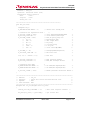
Contents
1. Specifications ................................................................................................ 2
2
Functions Used ............................................................................................. 3
3. Operation....................................................................................................... 6
4. Software ........................................................................................................ 8
5. Flowcharts ..................................................................................................... 11
6. Program Listing ............................................................................................. 14
REJ06B0357-0100O/Rev.1.00
March 2004
Page 1 of 17
SH7145F
Asynchronous Serial Data Transmission/Reception
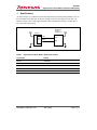
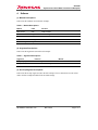
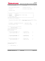
1. Specifications
As shown in figure 1, asynchronous serial data transmission is performed using channel 1 (ch1) of
the SCI module of the SH7145F. In this task example 3 bytes of serial data are received by the
SH7145, and the receive data is then transmitted. The communication format is 192,000 bps, 8bit, one stop bit, and no parity.
3.3 V
Serial data
transfer
target MCU
SH7145
TXD
SCI
(ch1)
RXD
3.3 V
RXD
TXD
Figure 1 Asynchronous Serial Data Transmission/Reception by SH7145
Table 1
Asynchronous Serial Data Transmission Format
Format Item
Setting
Bit rate
19200 bps
Data length
8 bits
Parity bit
No
Stop bit
1 bit
Serial/parallel conversion format
LSB first
REJ06B0357-0100O/Rev.1.00
March 2004
Page 2 of 17
SH7145F
Asynchronous Serial Data Transmission/Reception
2
Functions Used
In this task example the SCI (Serial Communication Interface) is used to perform asynchronous
serial data transmission/reception. Figure 2 shows a block diagram of channel 1 (ch1) of the SCI
module. The functions of the elements shown in figure 2 are described below.
SCI0 synchronous serial transfer function block
Transfer rate generator
SCI1 clock I/O pin
(SCK1)
External
clock
Baud rate generator
Bit rate register 1
(BRR_1)
On-chip
peripheral clock
Pφ/128
Pφ/32
Pφ/8
Pφ1
Clock
Transmit/receive operation control settings
Serial mode register 1
(SMR_1)
Serial control register 1
(SCR_1)
Transmit/receive
control circuit
Serial status register 1
(SSR_1)
Interrupt
requests
TEI_1
TXI_1
RXI_1
ERI_1
Serial direction control register 1
(SDCR_1)
Transmit data control
SCI1 transmit data
output pin
(TXD1)
Transmit shift register 1
(TSR_1)
Transmit data register 1
(TDR_1)
Receive data control
SCI1 receive data
input pin
(RXD1)
Receive shift register 1
(RSR_1)
Receive data register 1
(RDR_1)
Figure 2 SCI (ch1) Block Diagram
•
Asynchronous Mode
Serial data communication is performed using synchronization by character unit. This allows
serial communication with a standard dedicated asynchronous communication chip such as a
Universal Asynchronous Receiver/Transmitter (UART) or Asynchronous Communication
Interface Adapter (ACIA). In addition, the asynchronous mode supports serial communication
among multiple processors (multiprocessor communication function).
REJ06B0357-0100O/Rev.1.00
March 2004
Page 3 of 17
SH7145F
Asynchronous Serial Data Transmission/Reception
•
On-Chip Peripheral Clock Pφ
This is the reference clock for operation of on-chip peripheral functions. The clock signal is
generated by a clock oscillator.
•
Receive Shift Register (RSR_1)
This register is used to receive serial data. Serial data is input to RSR_1 from the RxD_1 pin.
When one frame of data has been received, it is automatically transferred to the receive data
register (RDR_1). RSR_1 cannot be accessed by the CPU.
•
Receive Data Register (RDR_1)
Received data is stored in this 8-bit register. When one frame of data has been received, it is
automatically transferred from RSR_1. RSR_1 and RDR_1 are in a double-buffer
configuration, allowing continuous reception of data. RDR_1 is a receive-only register, so it
can only be read by the CPU.
•
Transmit Shift Register (TSR_1)
This register is used to transmit serial data. In order to transmit data, the data is first
transferred from the transmit data register (TDR_1) to TSR_1. Then the transmit data is
output from the TxD_1 pin. TSR_1 cannot be accessed directly by the CPU.
•
Transmit Data Register (TDR_1)
Data to be transmitted is stored in this 8-bit register. When it is detected that TDR_1 is empty,
data that has been written to TDR_1 is automatically transferred to TSR_1. TDR_1 and
TSR_1 are in a double-buffer configuration. This allows data to be transferred to TSR_1 after
one frame of data has been transmitted and the next frame of data is still being written to
TDR_1, making possible continuous transmission of data. It is always possible to read or
write to the TDR from the CPU, but before writing to the TDR it should be confirmed that the
value of the TDRE bit in the serial status register (SSR_1) is 1.
•
Serial Mode Register (SMR_1)
This 8-bit register is used to select the serial data communication format and the clock source
for the on-chip baud rate generator.
•
Serial Control Register (SCR_1)
This register is used for transmit and receive control, interrupt control, and to select the
transmit and receive clock source.
•
Serial Status Register (SSR_1)
This register comprises the SCI1 status flag and the transmit and receive multiprocessor bits.
TDRE, RDRF, ORER, PER, and FER can be cleared only.
•
Serial Direction Control Register (SDCR_1)
This register is used to select whether the LSB or MSB is first. For 8-bit communication
either LSB-first or MSB-first may be selected, but LSB-first should be used for 7-bit
communication.
REJ06B0357-0100O/Rev.1.00
March 2004
Page 4 of 17
SH7145F
Asynchronous Serial Data Transmission/Reception
•
Bit Rate Register (BRR_1)
This 8-bit register is used to adjust the bit rate. The SCI has independent baud rate generators
for the individual channels, allowing different bit rates to be set for each. See the hardware
manual for details on setting values, execution rate relationships, etc.
Table 2 shows the function allocations for the task example.
Table 2
Function Allocations
Function
Classification
Function Allocation
TXD1
Pin
Channel 1 transmit data output pin
RXD1
Pin
Channel 1 transmit data input pin
SMR_1
SCI1
Sets communication format to asynchronous mode
SCR_1
SCI1
Enables transmit operation
SSR_1
SCI1
Status flag showing SCI1 operation status
SDCR_1
SCI1
Specifies LSB-first
BRR_1
SCI1
Sets communication bit rate
TSR_1
SCI1
Register for transmitting serial data
TDR_1
SCI1
Register for storing transmit data
RSR_1
SCI1
Register for receiving serial data
RDR_1
SCI1
Register for storing receive data
REJ06B0357-0100O/Rev.1.00
March 2004
Page 5 of 17
SH7145F
Asynchronous Serial Data Transmission/Reception
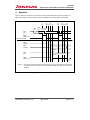
3. Operation
Figure 3 shows the operation of asynchronous mode data transmission in the task example. To
help explain figure 3, table 3 lists the software and hardware processing that is performed.
(1)
(2)
Start
bit
TxD1
(pin)
0
Data
bits
(3)
(6)
(4) (5) (7) (8)
(9)
(10)
(11)
(14)
(12) (13) (15)
Stop Start
bit bit
1
0
Data bits D0 to D7
RDRF
(SSR_1 bit)
Receive operation
Transmit operation
TDR_1
(register)
TSR_1
(register)
Start
bit
TXD1
(pin)
0
Data bits D0 to D7
TDRE
(SSR_1 bit)
Notes: 1. The start bit, transmit data, parity bit, and stop bit are output, in that order, from the TxD1 pin.
2. To perform continuous reception, read data transferred to RDR until reception of next data is
complete.
Figure 3
REJ06B0357-0100O/Rev.1.00
Data Transmission Operation
March 2004
Page 6 of 17
SH7145F
Asynchronous Serial Data Transmission/Reception
Table 3
Processing
Software Processing
Hardware Processing
(1)
—
RSR_1 receives serial data and transfers it
to RDR_1
(2)
—
Set RDRF flag in SSR_1 to 1
(3)
Read data from RDR_1
(4)
Clear RDRF flag in SSR_1 to 0
(5)
Write receive data to TDR_1
—
(6)
Clear TDRE flag in SSR_1 to 1
—
(7)
—
Transfer data from TDR_1 to TSR_1
(8)
—
Set TDRE flag in SSR_1 to 1 and output
transmit data from pin TXD1
(9)
—
RSR_1 receives serial data and transfers it
to RDR_1
(10)
—
Set RDRF flag in SSR_1 to 1
(11)
Read data from RDR_1
(12)
Clear RDRF flag in SSR_1 to 0
(13)
Write receive data to TDR_1
—
(14)
Clear TDRE flag in SSR_1 to 1
—
(15)
—
Transfer data from TDR_1 to TSR_1
(16)
Repeat
Repeat
REJ06B0357-0100O/Rev.1.00
March 2004
Page 7 of 17
SH7145F
Asynchronous Serial Data Transmission/Reception
4. Software
(1) Module Descriptions
Table 4 lists the modules used in the task example.
Table 4
Module Descriptions
Module
Label
Function
Main routine
main
Calls modules
SCI routine
init_sci
Initial settings of SCI1
Receive routine
rcv_sci
Receives serial data
Transmit routine
trans_sci
Transmits serial data
Error handling
err_int
Handles receive errors
(2) Argument Descriptions
Table 5 lists the arguments used in the task example.
Table 5
Argument Descriptions
Argument
Function
Module
Rev_data[0–2]
Stores SCI_1 receive data
Receive routine
trans_data
Transmits data from SCI_1
Transmit routine
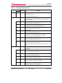
(3) On-Chip Register Descriptions
Table 6 lists the on-chip registers used in the task example. The set values shown are the values
used in the task example and differ from the initial settings.
REJ06B0357-0100O/Rev.1.00
March 2004
Page 8 of 17
SH7145F
Asynchronous Serial Data Transmission/Reception
Table 6
On-Chip Register Descriptions
Register
Bit
MSTCR1
MSTP17
Set Value
0
Function
Module standby control register 1
SCI1 standby control bit
Standby cancelled when MSTP17 = 0
SCR_1
H'70
Serial control register 1 (SCI_1)
Transmit and receive control, interrupt control, transmit and receive
clock source control
TIE
0
RIE
1
Transmit interrupt enable
TXI interrupt requests enabled when set to 1
Receive interrupt enable
RXI and ERI interrupt requests enabled when set to 1
TE
1
Transmit enable
Transmit operations enabled when set to 1
RE
1
Receive enable
Receive operations enabled when set to 1
MPIE
0
Multiprocessor interrupt enable
(In asynchronous mode, enabled when MP = 1 in SMR)
In the task example, disabled because MP = 0
TEIE
0
Transmit end interrupt enable
TEI interrupt requests enabled when set to 1
CKE1
0
Clock enable 1, 0
CKE2
0
Selects clock source and SCK pin function
In the task example, clock source is on-chip clock and SCK pin is not
used
SMR_1
H'00
Serial mode register 1
Selects communication format and the clock source for on-chip baud
rate generator
C/A
0
CHR
0
Communication mode
Asynchronous mode when cleared to 0
Character length (enabled in asynchronous mode only)
8-bit transmission and reception when 0
PE
0
Parity enable (enabled in asynchronous mode only)
No-parity transmission and reception when 0
O/E
0
Parity mode (enabled in asynchronous mode when PE = 1)
(In this example PE = 0 and this bit is disabled)
STOP
0
Stop bit length (enabled in asynchronous mode only)
1-stop-bit transmission and reception when 0
REJ06B0357-0100O/Rev.1.00
March 2004
Page 9 of 17
SH7145F
Asynchronous Serial Data Transmission/Reception
Register
Bit
SMR_1
Set Value
Function
MP
0
Multiprocessor mode (enabled in asynchronous mode only)
CKS1
0
Clock select 1, 0
CKS2
0
When value is 00, Pφ clock selected using on-chip baud rate generator
as clock source
Multiprocessor communication disabled when 0
BRR_1
H'40
Bit rate register 1
8-bit register for adjusting bit rate
SDCR_1
H'F2
Serial direction control register 1
DIR bit (bit 3) selects LSB-first or MSB-first
In task example, DIR = 0 (LSB-first)
SSR_1
H'xx
Serial status register 1
Comprises SCI1 status flag and transmit and receive multiprocessor bits
Only 0 may be written to the status flag, to clear it
PACRL2
TDRE
*
Transmit data register empty (status flag)
RDRF
*
Receive data register full (status flag)
ORER
*
Overrun error (status flag)
FER
*
Framing error (status flag)
PER
*
Parity error (status flag)
TEND
*
Transmit end (status flag)
MPB
0
Multiprocessor bit
MPBT
0
Multiprocessor bit transfer
PA4MD1
0
Port A control register L2
PA4MD0
1
Function setting for port A multiplex pin (TXD1)
PA3MD1
0
Port A control register L2
PA3MD0
1
Function setting for port A multiplex pin (RXD1)
*: Can only be cleared to 0. Setting to 1 is performed by hardware.
REJ06B0357-0100O/Rev.1.00
March 2004
Page 10 of 17
SH7145F
Asynchronous Serial Data Transmission/Reception
5. Flowcharts
(1) Main Routine
main()
Initialize SCI module
init_sci()
rcv_sci()
Receive 1st byte of data
rcv_sci()
Receive 2nd byte of data
rcv_sci()
Receive 3rd byte of data
REJ06B0357-0100O/Rev.1.00
March 2004
Page 11 of 17
SH7145F
Asynchronous Serial Data Transmission/Reception
(2) SCI1 Initialize Routine
init_sci()
Cancel SCI1 module standby status
Clear to 0 bits TIE, RIE, TE, RE, MPIE,
and TEIE in SCR_0
Select on-chip clock as clock source
using CKE1 and CKE0 in SCR_0
Using SMR_1, select asynchronous
mode, 8 data bits, no parity, 1 stop bit,
and Pφ as baud rate generator clock
source
Using BRR_1, set communication
speed to 19,200 bps
Using DIR bit in SDCR_1, select
LSB-first communication
Wait minimum
1-bit transfer time
No
Yes
Using SCR_1, enable ERI interrupt
Using PACRL2, set PA3 (pin 133) to
RXD function and PA4 (pin 134)
to RXD function
Set bits TE and RE in SCR_1 to 1 to
enable transmit operation and receive
operation
RTE
REJ06B0357-0100O/Rev.1.00
March 2004
Page 12 of 17
SH7145F
Asynchronous Serial Data Transmission/Reception
(3) Data Receive Routine
rcv_sci()
Wait until
RDR_1 finishes receiving
data
No
Yes
Read receive data from RDR_1 and
store it in on-chip RAM
Clear RDRF flag in SSR_1 to 0
Transmit receive data without
modification
RTE
(4) Data Transfer Routine
trans_sci()
Wait until
possible to write to
TDR_1
No
Yes
Write transmit data to TDR_1
Clear TDRE bit in SSR_1 to 0
RTE
REJ06B0357-0100O/Rev.1.00
March 2004
Page 13 of 17
SH7145F
Asynchronous Serial Data Transmission/Reception
6. Program Listing
/**************************************************************/
/* SH7145F Application Note
*/
/*
*/
/* Function
*/
/*
:SCI1
*/
/*
*/
/* External input clock
: 12.5MHz
*/
/* Internal CPU clock
: 50MHz
*/
/* Internal peripheral clock : 25MHz
*/
/*
*/
/* Written
:2003/7
Rev.1.0
*/
/**************************************************************/
#include "iodefine.h"
#include <machine.h>
/*------------ Symbol Definition ----------------------------------------------*/
#define COUNT 3
/*------------ Function Definition --------------------------------------------*/
void main(void);
void init_sci(void);
unsigned char rcv_sci(unsigned char);
void trans_sci(char);
void err_int(void);
void dummy_f(void);
/*------------ RAM allocation Definition --------------------------------------*/
volatile unsigned char Rev_data[COUNT];
/**************************************************************/
/* main Program
*/
/**************************************************************/
void main( void )
{
unsigned char i = 0;
init_sci();
i = rcv_sci(i);
i = rcv_sci(i);
i = rcv_sci(i);
while(1);
/*
/*
/*
/*
/*
Initialize SCI
Receive 1st byte of serial data
Receive 2nd byte of serial data
Receive 3rd byte of serial data
LOOP
*/
*/
*/
*/
*/
}
/**************************************************************
REJ06B0357-0100O/Rev.1.00
March 2004
Page 14 of 17
SH7145F
Asynchronous Serial Data Transmission/Reception
Function : init_sci
Operation : Initialize serial (sci1)
Asynchronous receive operation
-Data
: 8bit
-Stop bit
: 1bit
-Parity bit : No
**************************************************************/
void init_sci(void)
{
unsigned long i;
P_STBY.MSTCR1.BIT.MSTP17 = 0;
/* disable SCI1 standby mode
/* Initialize SCI Asynchronous mode *
P_SCI1.SCR_1.BYTE &= 0x03 ;
/*
P_SCI1.SCR_1.BIT.CKE = 0;
/*
P_SCI1.SMR_1.BYTE = 0x00;
/*
//
CA = 0;
/*
//
CHR = 0;
/*
//
PE = 0;
/*
//
OE = 0;
/*
//
STOP = 0;
/*
//
CKS = 0;
/*
*/
*/
clear TIE,RIE,TE,RE,MPIE,TEIE
clock:internal,SCK:output
8bit,No parity,1stop bit
Asynchronous mode
data length 8bits
No parity
(=0)even parity
1 stop bit
clock source=Pφ(25MHz)
*/
*/
*/
*/
*/
*/
*/
*/
*/
P_SCI1.BRR_1 = 40;
P_SCI1.SDCR_1.BIT.DIR = 0;
/* 19200bps@25MHz(Peripheral)
/* LSB first send
*/
*/
for( i=0; i < 0x0300 ; i++);
/* Wait 1bit
*/
P_SCI1.SCR_1.BIT.TIE = 0;
P_SCI1.SCR_1.BIT.RIE = 0;
/* TXI1 interrupt disable
/* RXI1,ERI interrupt disable
*/
*/
*/
/* set TXD1(PA4:134pin@SH7145)
/* set RXD1(PA3:133pin@SH7145)
*/
*/
/* Initialize SCI1 PORT
P_PORTA.PACRL2.BIT.PA4MD = 1;
P_PORTA.PACRL2.BIT.PA3MD = 1;
P_SCI1.SCR_1.BYTE |= 0x30;
/* TE=RE=1,Transmit and Receive Enable */
}
/******************************************************************************/
/* Function
: rcv_sci
*/
/* Operation
: Serial data receive and send function calls
*/
/* Argument
: None
*/
/* Value returned : None
*/
/******************************************************************************/
unsigned char rcv_sci(unsigned char rev_count)
{
while(P_SCI1.SSR_1.BIT.RDRF == 0);
/* Wait until reception finishes */
Rev_data[rev_count] = P_SCI1.RDR_1;
REJ06B0357-0100O/Rev.1.00
/* get receive data
March 2004
*/
Page 15 of 17
SH7145F
Asynchronous Serial Data Transmission/Reception
P_SCI1.SSR_1.BIT.RDRF = 0;
/* Clear RDRF
*/
trans_sci(Rev_data[rev_count]);
/* Transmit receive data
*/
rev_count++ ;
/* Increment storage address
*/
return(rev_count);
}
/************************************************************************/
/* Function
: trans_sci
*/
/* Operation
: Write 1 character to serial output
*/
/* Argument
: trans_data
*/
/* Value returned : None
*/
/************************************************************************/
void trans_sci(char tarans_data) {
while(!(P_SCI1.SSR_1.BYTE & 0x80)){ /* Wait until data can be written to TDR */
;
/* (until TDRE is set to 1)
*/
}
P_SCI1.TDR_1 = (unsigned char)trans_data;
P_SCI1.SSR_1.BYTE &= 0x7F;
/* Write data to TDR
/* Clear flag, transmit
*/
*/
}
/**************************************
Interrupt handling
**************************************/
#pragma interrupt(err_int)
void err_int(void)
{
if(P_SCI1.SSR_1.BIT.ORER == 1){
P_SCI1.SSR_1.BIT.ORER = 0;
}
/* Overrun error
/* ORER flag clear
*/
*/
if(P_SCI1.SSR_1.BIT.FER == 1){
P_SCI1.SSR_1.BIT.FER = 0;
}
/* Framing error
/* FER flag clear
*/
*/
if(P_SCI1.SSR_1.BIT.PER == 1){
P_SCI1.SSR_1.BIT.PER = 0;
}
/* Parity error
/* PER flag clear
*/
*/
}
#pragma interrupt(dummy_f)
void dummy_f(void)
{
/*
Other Interrupt
*/
}
REJ06B0357-0100O/Rev.1.00
March 2004
Page 16 of 17
SH7145F
Asynchronous Serial Data Transmission/Reception
Keep safety first in your circuit designs!
1. Renesas Technology Corp. puts the maximum effort into making semiconductor products better and
more reliable, but there is always the possibility that trouble may occur with them. Trouble with
semiconductors may lead to personal injury, fire or property damage.
Remember to give due consideration to safety when making your circuit designs, with appropriate
measures such as (i) placement of substitutive, auxiliary circuits, (ii) use of nonflammable material or
(iii) prevention against any malfunction or mishap.
Notes regarding these materials
1. These materials are intended as a reference to assist our customers in the selection of the Renesas
Technology Corp. product best suited to the customer's application; they do not convey any license
under any intellectual property rights, or any other rights, belonging to Renesas Technology Corp. or
a third party.
2. Renesas Technology Corp. assumes no responsibility for any damage, or infringement of any thirdparty's rights, originating in the use of any product data, diagrams, charts, programs, algorithms, or
circuit application examples contained in these materials.
3. All information contained in these materials, including product data, diagrams, charts, programs and
algorithms represents information on products at the time of publication of these materials, and are
subject to change by Renesas Technology Corp. without notice due to product improvements or
other reasons. It is therefore recommended that customers contact Renesas Technology Corp. or
an authorized Renesas Technology Corp. product distributor for the latest product information
before purchasing a product listed herein.
The information described here may contain technical inaccuracies or typographical errors.
Renesas Technology Corp. assumes no responsibility for any damage, liability, or other loss rising
from these inaccuracies or errors.
Please also pay attention to information published by Renesas Technology Corp. by various means,
including the Renesas Technology Corp. Semiconductor home page (http://www.renesas.com).
4. When using any or all of the information contained in these materials, including product data,
diagrams, charts, programs, and algorithms, please be sure to evaluate all information as a total
system before making a final decision on the applicability of the information and products. Renesas
Technology Corp. assumes no responsibility for any damage, liability or other loss resulting from the
information contained herein.
5. Renesas Technology Corp. semiconductors are not designed or manufactured for use in a device or
system that is used under circumstances in which human life is potentially at stake. Please contact
Renesas Technology Corp. or an authorized Renesas Technology Corp. product distributor when
considering the use of a product contained herein for any specific purposes, such as apparatus or
systems for transportation, vehicular, medical, aerospace, nuclear, or undersea repeater use.
6. The prior written approval of Renesas Technology Corp. is necessary to reprint or reproduce in
whole or in part these materials.
7. If these products or technologies are subject to the Japanese export control restrictions, they must
be exported under a license from the Japanese government and cannot be imported into a country
other than the approved destination.
Any diversion or reexport contrary to the export control laws and regulations of Japan and/or the
country of destination is prohibited.
8. Please contact Renesas Technology Corp. for further details on these materials or the products
contained therein.
REJ06B0357-0100O/Rev.1.00
March 2004
Page 17 of 17