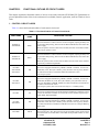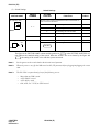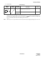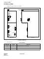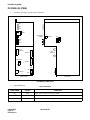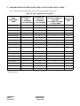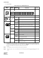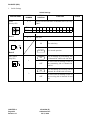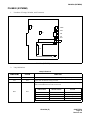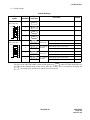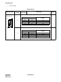
1
ND-45504 (E)
ISSUE 2
PART OF STOCK # 151900
®
Circuit Card Manual
DECEMBER, 1997
NEC America, Inc.
LIABILITY DISCLAIMER
NEC America Inc. reserves the right to change the specifications,
functions, or features, at any time, without notice.
NEC America Inc. has prepared this document for use by its employees and customers. The information contained herein is the
property of NEC America Inc. and shall not be reproduced without
prior written approval from NEC America Inc.
NEAX and Dterm are registered trademarks of NEC Corporation.
Copyright 1997
NEC America Inc.
Printed in the U.S.A.
PAGE No.
ADD. No.
001
i
002
003
004
005
006
007
008
2.2
ii
2.1
PAGE No.
36
2.2
iv
38
1
39
40
2.2
4
2.1
42
5
2.1
43
6
44
7
45
004
005
006
007
008
2.1
2.2
2.2
46
9
2.2
47
10
2.2
48
11
2.2
49
12
2.2
50
13
14
51
2.1
52
15
53
16
54
17
55
18
56
19
57
20
2.2
59
22
60
23
61
24
62
25
63
26
64
27
65
28
29
2.1
30
31
65-1
2.1
65-2
2.1
65-3
2.1
2.2
65-4
2.1
2.2
66
33
2.2
67
34
2.2
32
2.1
58
21
2.1
JULY, 1998
ADDENDUM-002
DATE
ADDENDUM-005
DATE
NEAX2000 IVS
Circuit Card Manual
2.1
68
ADDENDUM-001
DATE
003
2.2
41
8
002
2.2
37
3
001
35
iii
2
ADD. No.
OCTOBER, 1998
ADDENDUM-003
DATE
ADDENDUM-006
DATE
ADDENDUM-004
DATE
ADDENDUM-007
DATE
ADDENDUM-008
DATE
Addendum Revision Sheet 1/2
ND-45504 (E) ISSUE 2
PAGE No.
ADD. No.
001
002
003
004
005
006
007
008
PAGE No.
68-1
2.1
97
68-2
2.1
98
68-3
2.1
99
68-4
2.1
100
69
2.1
102
71
2.1
103
72
104
73
105
74
106
75
107
76
108
77
109
78
002
003
004
005
006
007
008
110
2.1
111
78-2
2.1
112
78-3
2.1
113
78-4
2.1
114
78-5
2.1
115
78-6
2.1
116
79
117
80
118
81
119
82
120
83
121
84
122
85
123
86
124
87
125
88
126
89
127
90
128
91
129
92
130
93
131
94
132
95
133
96
134
ADDENDUM-001
DATE
001
101
70
78-1
ADD. No.
JULY, 1998
ADDENDUM-002
DATE
ADDENDUM-005
DATE
NEAX2000 IVS
Circuit Card Manual
OCTOBER, 1998
ADDENDUM-003
DATE
ADDENDUM-006
DATE
ADDENDUM-004
DATE
ADDENDUM-007
DATE
ADDENDUM-008
DATE
Addendum Revision Sheet 2/2
ND-45504 (E) ISSUE 2
ND-45504 (E)
ISSUE 2
DECEMBER, 1997
NEAX2000 IVS
Circuit Card Manual
TABLE OF CONTENTS
Page
LIST OF FIGURES . . . . . . . . . . . . . . . . . . . . . . . . . . . . . . . . . . . . . . . . . . . . . . . . . . . . . . . . . . . . . . . . . . . . . . . . . iii
LIST OF TABLES . . . . . . . . . . . . . . . . . . . . . . . . . . . . . . . . . . . . . . . . . . . . . . . . . . . . . . . . . . . . . . . . . . . . . . . . . . iv
CHAPTER 1
INTRODUCTION . . . . . . . . . . . . . . . . . . . . . . . . . . . . . . . . . . . . . . . . . . . . . . . . . . . . . . . . . . 1
1. PURPOSE . . . . . . . . . . . . . . . . . . . . . . . . . . . . . . . . . . . . . . . . . . . . . . . . . . . . . . . . . . . . . . . . . . . . . . . . . 1
2. OUTLINE OF THE MANUAL . . . . . . . . . . . . . . . . . . . . . . . . . . . . . . . . . . . . . . . . . . . . . . . . . . . . . . . . . . . 1
CHAPTER 2
FUNCTIONAL OUTLINE OF CIRCUIT CARDS . . . . . . . . . . . . . . . . . . . . . . . . . . . . . . . . . . . 3
1. CONTROL CIRCUIT CARDS . . . . . . . . . . . . . . . . . . . . . . . . . . . . . . . . . . . . . . . . . . . . . . . . . . . . . . . . . . 3
2. APPLICATION CIRCUIT CARDS . . . . . . . . . . . . . . . . . . . . . . . . . . . . . . . . . . . . . . . . . . . . . . . . . . . . . . . 4
3. LINE/TRUNK CIRCUIT CARDS. . . . . . . . . . . . . . . . . . . . . . . . . . . . . . . . . . . . . . . . . . . . . . . . . . . . . . . . . 6
CHAPTER 3
CIRCUIT CARD INSTALLATION CONDITIONS . . . . . . . . . . . . . . . . . . . . . . . . . . . . . . . . . . 9
1. CIRCUIT CARD MOUNTING SLOTS . . . . . . . . . . . . . . . . . . . . . . . . . . . . . . . . . . . . . . . . . . . . . . . . . . . . 9
2. INSTALLATION CONDITIONS FOR CONTROL CIRCUIT CARDS . . . . . . . . . . . . . . . . . . . . . . . . . . . . 11
2.1
PN-CP00/PN-CP00-B/PN-CP00-C (MP) . . . . . . . . . . . . . . . . . . . . . . . . . . . . . . . . . . . . . . . . . . 11
2.2
PN-CP01 (FP) . . . . . . . . . . . . . . . . . . . . . . . . . . . . . . . . . . . . . . . . . . . . . . . . . . . . . . . . . . . . . . . 11
2.3
PN-CP02/PN-CP02-C (MP) . . . . . . . . . . . . . . . . . . . . . . . . . . . . . . . . . . . . . . . . . . . . . . . . . . . . 12
2.4
PN-BS00-A/PN-BS00-B (BS00), PN-BS01-A/PN-BS01-B (BS01) . . . . . . . . . . . . . . . . . . . . . . . 13
2.5
PN-PW00 (EXTPWR) . . . . . . . . . . . . . . . . . . . . . . . . . . . . . . . . . . . . . . . . . . . . . . . . . . . . . . . . . 13
2.6
PZ-PW86 (PWR) . . . . . . . . . . . . . . . . . . . . . . . . . . . . . . . . . . . . . . . . . . . . . . . . . . . . . . . . . . . . . 13
3. INSTALLATION CONDITIONS FOR APPLICATION CIRCUIT CARDS . . . . . . . . . . . . . . . . . . . . . . . . . 14
4. INSTALLATION CONDITIONS FOR LINE/TRUNK CIRCUIT CARDS . . . . . . . . . . . . . . . . . . . . . . . . . . 16
CHAPTER 4
LAMP INDICATIONS AND SWITCH SETTINGS . . . . . . . . . . . . . . . . . . . . . . . . . . . . . . . . . 17
1. PRECAUTION IN HANDLING . . . . . . . . . . . . . . . . . . . . . . . . . . . . . . . . . . . . . . . . . . . . . . . . . . . . . . . . . 18
2. LAMP INDICATIONS AND SWITCH SETTINGS OF CONTROL CIRCUIT CARDS. . . . . . . . . . . . . . . . 21
PN-BS00-A/PN-BS00-B (BS00). . . . . . . . . . . . . . . . . . . . . . . . . . . . . . . . . . . . . . . . . . . . . . . . . . . . . . . . 22
PN-BS01-A (BS01) . . . . . . . . . . . . . . . . . . . . . . . . . . . . . . . . . . . . . . . . . . . . . . . . . . . . . . . . . . . . . . . . . 24
PN-BS01-B (BS01) . . . . . . . . . . . . . . . . . . . . . . . . . . . . . . . . . . . . . . . . . . . . . . . . . . . . . . . . . . . . . . . . . 26
PN-CP00 (MP) . . . . . . . . . . . . . . . . . . . . . . . . . . . . . . . . . . . . . . . . . . . . . . . . . . . . . . . . . . . . . . . . . . . . . 28
PN-CP00-B/PN-CP00-C (MP) . . . . . . . . . . . . . . . . . . . . . . . . . . . . . . . . . . . . . . . . . . . . . . . . . . . . . . . . . 31
PN-CP03/PN-CP03-C (MP) . . . . . . . . . . . . . . . . . . . . . . . . . . . . . . . . . . . . . . . . . . . . . . . . . . . . . . . . . . . 34
PN-CP01 (FP) . . . . . . . . . . . . . . . . . . . . . . . . . . . . . . . . . . . . . . . . . . . . . . . . . . . . . . . . . . . . . . . . . . . . . 37
PN-CP02/PN-CP02-C (MP) . . . . . . . . . . . . . . . . . . . . . . . . . . . . . . . . . . . . . . . . . . . . . . . . . . . . . . . . . . . 39
PN-PW00 (EXTPWR) . . . . . . . . . . . . . . . . . . . . . . . . . . . . . . . . . . . . . . . . . . . . . . . . . . . . . . . . . . . . . . . 42
PZ-PW86 (PWR) . . . . . . . . . . . . . . . . . . . . . . . . . . . . . . . . . . . . . . . . . . . . . . . . . . . . . . . . . . . . . . . . . . . 44
PZ-PW86-A (PWR) . . . . . . . . . . . . . . . . . . . . . . . . . . . . . . . . . . . . . . . . . . . . . . . . . . . . . . . . . . . . . . . . . 46
PZ-PW86 (C) (PWR) . . . . . . . . . . . . . . . . . . . . . . . . . . . . . . . . . . . . . . . . . . . . . . . . . . . . . . . . . . . . . . . . 48
PZ-PW86 (D) (PWR) . . . . . . . . . . . . . . . . . . . . . . . . . . . . . . . . . . . . . . . . . . . . . . . . . . . . . . . . . . . . . . . . 50
ND-45504 (E)
Addendum-002
OCTOBER, 1998
TABLE OF CONTENTS
Page i
Revision 2.2
Page
3. LAMP INDICATIONS AND SWITCH SETTINGS OF APPLICATION CIRCUIT CARDS . . . . . . . . . . . . . 52
PN-AP00-A (AP00) . . . . . . . . . . . . . . . . . . . . . . . . . . . . . . . . . . . . . . . . . . . . . . . . . . . . . . . . . . . . . . . . . . 53
PN-AP01 (AP01) . . . . . . . . . . . . . . . . . . . . . . . . . . . . . . . . . . . . . . . . . . . . . . . . . . . . . . . . . . . . . . . . . . . . 59
PN-BRTA (BRI) . . . . . . . . . . . . . . . . . . . . . . . . . . . . . . . . . . . . . . . . . . . . . . . . . . . . . . . . . . . . . . . . . . . . . 62
PN-2BRTC (BRI). . . . . . . . . . . . . . . . . . . . . . . . . . . . . . . . . . . . . . . . . . . . . . . . . . . . . . . . . . . . . . . . . . . 65-1
PN-CC00 (ETHER) . . . . . . . . . . . . . . . . . . . . . . . . . . . . . . . . . . . . . . . . . . . . . . . . . . . . . . . . . . . . . . . . . . 66
PN-CC01 (ETHER) . . . . . . . . . . . . . . . . . . . . . . . . . . . . . . . . . . . . . . . . . . . . . . . . . . . . . . . . . . . . . . . . . 68-1
PN-CK00 (PLO) . . . . . . . . . . . . . . . . . . . . . . . . . . . . . . . . . . . . . . . . . . . . . . . . . . . . . . . . . . . . . . . . . . . . 69
PN-24DTA (DTI) . . . . . . . . . . . . . . . . . . . . . . . . . . . . . . . . . . . . . . . . . . . . . . . . . . . . . . . . . . . . . . . . . . . . 72
PN-24DTA-A (DTI) . . . . . . . . . . . . . . . . . . . . . . . . . . . . . . . . . . . . . . . . . . . . . . . . . . . . . . . . . . . . . . . . . . 75
PN-30DTC/30DTC-A (DTI) . . . . . . . . . . . . . . . . . . . . . . . . . . . . . . . . . . . . . . . . . . . . . . . . . . . . . . . . . . . 78-1
PN-ME00 (EXTMEM) . . . . . . . . . . . . . . . . . . . . . . . . . . . . . . . . . . . . . . . . . . . . . . . . . . . . . . . . . . . . . . . . 79
PN-4RSTB (MFR) . . . . . . . . . . . . . . . . . . . . . . . . . . . . . . . . . . . . . . . . . . . . . . . . . . . . . . . . . . . . . . . . . . . 84
PN-4RSTC (CIR). . . . . . . . . . . . . . . . . . . . . . . . . . . . . . . . . . . . . . . . . . . . . . . . . . . . . . . . . . . . . . . . . . . . 86
PN-SC00 (CCH) . . . . . . . . . . . . . . . . . . . . . . . . . . . . . . . . . . . . . . . . . . . . . . . . . . . . . . . . . . . . . . . . . . . . 88
PN-SC01 (DCH) . . . . . . . . . . . . . . . . . . . . . . . . . . . . . . . . . . . . . . . . . . . . . . . . . . . . . . . . . . . . . . . . . . . . 91
PN-SC02 (ICH) . . . . . . . . . . . . . . . . . . . . . . . . . . . . . . . . . . . . . . . . . . . . . . . . . . . . . . . . . . . . . . . . . . . . . 94
PN-SC03 (ICH) . . . . . . . . . . . . . . . . . . . . . . . . . . . . . . . . . . . . . . . . . . . . . . . . . . . . . . . . . . . . . . . . . . . . . 96
PN-SC03 (CSH) . . . . . . . . . . . . . . . . . . . . . . . . . . . . . . . . . . . . . . . . . . . . . . . . . . . . . . . . . . . . . . . . . . . . 98
4. LAMP INDICATIONS AND SWITCH SETTINGS OF LINE/TRUNK CIRCUIT CARDS . . . . . . . . . . . . . 100
PN-2AMPA (AMP). . . . . . . . . . . . . . . . . . . . . . . . . . . . . . . . . . . . . . . . . . . . . . . . . . . . . . . . . . . . . . . . . . 101
PN-AUCA (AUC) . . . . . . . . . . . . . . . . . . . . . . . . . . . . . . . . . . . . . . . . . . . . . . . . . . . . . . . . . . . . . . . . . . . 102
PN-CFTA (CFT) . . . . . . . . . . . . . . . . . . . . . . . . . . . . . . . . . . . . . . . . . . . . . . . . . . . . . . . . . . . . . . . . . . . 103
PN-4COTB (COT) . . . . . . . . . . . . . . . . . . . . . . . . . . . . . . . . . . . . . . . . . . . . . . . . . . . . . . . . . . . . . . . . . . 104
PN-4COTG (COT). . . . . . . . . . . . . . . . . . . . . . . . . . . . . . . . . . . . . . . . . . . . . . . . . . . . . . . . . . . . . . . . . . 105
PN-2DATA (DAT) . . . . . . . . . . . . . . . . . . . . . . . . . . . . . . . . . . . . . . . . . . . . . . . . . . . . . . . . . . . . . . . . . . 106
PN-DK00 (DK). . . . . . . . . . . . . . . . . . . . . . . . . . . . . . . . . . . . . . . . . . . . . . . . . . . . . . . . . . . . . . . . . . . . . 108
PN-4DITB (DIT). . . . . . . . . . . . . . . . . . . . . . . . . . . . . . . . . . . . . . . . . . . . . . . . . . . . . . . . . . . . . . . . . . . . 109
PN-2DLCB (DLC) . . . . . . . . . . . . . . . . . . . . . . . . . . . . . . . . . . . . . . . . . . . . . . . . . . . . . . . . . . . . . . . . . . 110
PN-2DLCC (DLC) . . . . . . . . . . . . . . . . . . . . . . . . . . . . . . . . . . . . . . . . . . . . . . . . . . . . . . . . . . . . . . . . . . 111
PN-2DLCN (DLC) . . . . . . . . . . . . . . . . . . . . . . . . . . . . . . . . . . . . . . . . . . . . . . . . . . . . . . . . . . . . . . . . . . 112
PN-4DLCA (DLC) . . . . . . . . . . . . . . . . . . . . . . . . . . . . . . . . . . . . . . . . . . . . . . . . . . . . . . . . . . . . . . . . . . 113
PN-4DLCD (DLC) . . . . . . . . . . . . . . . . . . . . . . . . . . . . . . . . . . . . . . . . . . . . . . . . . . . . . . . . . . . . . . . . . . 114
PN-4DLCF (DLC) . . . . . . . . . . . . . . . . . . . . . . . . . . . . . . . . . . . . . . . . . . . . . . . . . . . . . . . . . . . . . . . . . . 115
PN-4DLCM (DLC) . . . . . . . . . . . . . . . . . . . . . . . . . . . . . . . . . . . . . . . . . . . . . . . . . . . . . . . . . . . . . . . . . . 116
PN-4DLCQ (DLC) . . . . . . . . . . . . . . . . . . . . . . . . . . . . . . . . . . . . . . . . . . . . . . . . . . . . . . . . . . . . . . . . . . 117
PN-2DPCB (DPC) . . . . . . . . . . . . . . . . . . . . . . . . . . . . . . . . . . . . . . . . . . . . . . . . . . . . . . . . . . . . . . . . . . 118
PN-2ILCA (ILC) . . . . . . . . . . . . . . . . . . . . . . . . . . . . . . . . . . . . . . . . . . . . . . . . . . . . . . . . . . . . . . . . . . . . 121
PN-4LCD/4LCD-A (LC) . . . . . . . . . . . . . . . . . . . . . . . . . . . . . . . . . . . . . . . . . . . . . . . . . . . . . . . . . . . . . . 124
PN-4LCJ (LC) . . . . . . . . . . . . . . . . . . . . . . . . . . . . . . . . . . . . . . . . . . . . . . . . . . . . . . . . . . . . . . . . . . . . . 125
PN-M03 (M03). . . . . . . . . . . . . . . . . . . . . . . . . . . . . . . . . . . . . . . . . . . . . . . . . . . . . . . . . . . . . . . . . . . . . 126
PN-2ODTA (ODT) . . . . . . . . . . . . . . . . . . . . . . . . . . . . . . . . . . . . . . . . . . . . . . . . . . . . . . . . . . . . . . . . . . 129
PN-8RSTA (PBR) . . . . . . . . . . . . . . . . . . . . . . . . . . . . . . . . . . . . . . . . . . . . . . . . . . . . . . . . . . . . . . . . . . 130
PN-TNTA (TNT) . . . . . . . . . . . . . . . . . . . . . . . . . . . . . . . . . . . . . . . . . . . . . . . . . . . . . . . . . . . . . . . . . . . 131
PN-2CSIA (CSI) . . . . . . . . . . . . . . . . . . . . . . . . . . . . . . . . . . . . . . . . . . . . . . . . . . . . . . . . . . . . . . . . . . . 133
TABLE OF CONTENTS
Page ii
Revision 2.1
ND-45504 (E)
Addendum-001
JULY, 1998
LIST OF FIGURES
Figure
3-1
3-2
3-3
3-4
3-5
3-6
4-1
4-2
Title
Page
Circuit Card Mounting Slots . . . . . . . . . . . . . . . . . . . . . . . . . . . . . . . . . . . . . . . . . . . . . . . . . . . . . . . . . . . 9
MP/FP Card Mounting Slots . . . . . . . . . . . . . . . . . . . . . . . . . . . . . . . . . . . . . . . . . . . . . . . . . . . . . . . . . . 11
MP/FP Card Mounting Slots for Back up MP System . . . . . . . . . . . . . . . . . . . . . . . . . . . . . . . . . . . . . . 12
BS00/BS01 Card Mounting Slots . . . . . . . . . . . . . . . . . . . . . . . . . . . . . . . . . . . . . . . . . . . . . . . . . . . . . . 13
Application Circuit Card Mounting Slots . . . . . . . . . . . . . . . . . . . . . . . . . . . . . . . . . . . . . . . . . . . . . . . . . 15
Line/Trunk Circuit Card Mounting Slots . . . . . . . . . . . . . . . . . . . . . . . . . . . . . . . . . . . . . . . . . . . . . . . . . 16
Static Electricity Precautions (1 of 2) . . . . . . . . . . . . . . . . . . . . . . . . . . . . . . . . . . . . . . . . . . . . . . . . . . . 18
Circuit Card Handling Precautions . . . . . . . . . . . . . . . . . . . . . . . . . . . . . . . . . . . . . . . . . . . . . . . . . . . . . 20
ND-45504 (E)
LIST OF FIGURES
Page iii
Revision 2.0
LIST OF TABLES
Table
2-1
2-2
2-3
4-1
4-2
4-3
Title
Page
Functional Outline of Control Circuit Cards . . . . . . . . . . . . . . . . . . . . . . . . . . . . . . . . . . . . . . . . . . . .
Functional Outline of Application Circuit Cards . . . . . . . . . . . . . . . . . . . . . . . . . . . . . . . . . . . . . . . . .
Functional Outline of Line/Trunk Circuit Cards . . . . . . . . . . . . . . . . . . . . . . . . . . . . . . . . . . . . . . . . .
Table of Control Circuit Cards . . . . . . . . . . . . . . . . . . . . . . . . . . . . . . . . . . . . . . . . . . . . . . . . . . . . . .
Table of Application Circuit Cards . . . . . . . . . . . . . . . . . . . . . . . . . . . . . . . . . . . . . . . . . . . . . . . . . . .
Table of Line /Trunk Circuit Cards . . . . . . . . . . . . . . . . . . . . . . . . . . . . . . . . . . . . . . . . . . . . . . . . . . .
... 3
... 4
... 6
. . 21
. . 52
. 100
LIST OF TABLES
Page iv
Revision 2.0
ND-45504 (E)
CHAPTER 1
INTRODUCTION
1. PURPOSE
For installers and maintenance technicians of the NEAX2000 IVS (PBX), this manual explains the functional
outline and installation conditions of the circuit cards, and explains the meaning of each indicator lamp (LED)
and the switch settings on the circuit cards.
2. OUTLINE OF THE MANUAL
This manual consists of four chapters. The contents of Chapter 2 through 4 are as outlined below.
•
Chapter 2: Functional Outline of Circuit Cards
This chapter outlines various circuit cards used in the system by means of tables.
•
Chapter 3: Circuit Card Accommodating Conditions
This chapter explains the conditions for installing various circuit cards used in the system.
•
Chapter 4: Lamp Indications and Switch Settings
This chapter explains the meaning of lamp indications and the switch settings of various circuit cards used
in the system.
Each switch setting table provided in Chapter 4 has a “CHECK” column. Make necessary entries in the CHECK
column during and/or after system installation and maintenance. After the result of switch setting has been
checked, use each table as a reference for subsequent system maintenance and operations.
ND-45504 (E)
CHAPTER 1
Page 1
Revision 2.0
This page is for your notes.
CHAPTER 1
Page 2
Revision 2.0
ND-45504 (E)
CHAPTER 2
FUNCTIONAL OUTLINE OF CIRCUIT CARDS
This chapter explains the functional outline of various circuit cards used in the NEAX2000 IVS. Explanations are
given in alphabetical order of the circuit card names for each kind (Control, Application, and Line/Trunk) of circuit
cards.
1. CONTROL CIRCUIT CARDS
Table 2-1 shows the functional outline of each control circuit card.
Table 2-1 Functional Outline of Control Circuit Cards
CARD NAME
PN-BS00-A
/PN-BS00-B
PN-BS01-A
/PN-BS01-B
PN-CP00
/PN-CP00-B
/PN-CP00-C
PN-CP03
/PN-CP03-C
PN-CP01
PN-CP02
/PN-CP02-C
PN-PW00
FUNCTIONAL
NAME
FUNCTIONAL OUTLINE
BS00
Bus interface card for PIM0.
This card functions as a driver/receiver of various signals, adjusts gate delay timing and cable delay timing, monitors the I/O Bus and PCM Bus, and controls the
power supply.
When the system consists of more than one PIM, this card is mounted in PIM0.
Only one per system is used.
BS01
Bus interface card for PIM1 through PIM7.
This card functions as a driver/receiver of various signals, adjusts gate delay timing and cable delay timing, monitors the I/O Bus and PCM Bus, and controls the
power supply.
When the system consists of more than one PIM, one each of this card is mounted
respectively in PIM1 through PIM7.
MP
Main Processor card.
This card is equipped with Memory, TDSW (1024CH × 1024CH), 16-Line CFT,
PB Sender, Clock, PLO (slave mode 2 ports), RS-232C Ports (2 ports), Modem
for remote maintenance, and Internal Music-On-Hold tone source.
One card per system.
MP
Main Processor card.
This card is equipped with Memory, TDSW (1024CH × 1024CH), 16-Line CFT,
PB Sender, PB Receiver, Clock, PLO (slave mode 2 ports), RS-232C Ports (2
ports) for MAT/Built-in SMDR, Modem for remote maintenance, Internal/External Music-On-Hold tone source.
One card per system (This card can be used only in 1 or 2 PIM system).
FP
Firmware Processor card.
This card is equipped with Line/Trunk Interface and Memory. When the system
consists of more than one PIM, one each of this card is mounted respectively in
PIM0, PIM2, PIM4 and PIM6.
MP
Main Processor card for Back Up MP System only.
This card is equipped with Memory, TDSW (1024CH × 1024CH), 16-Line CFT,
PB Sender, Clock, PLO (slave mode 2 ports), RS-232C Ports (2 ports), Modem
for remote maintenance, and Music-On-Hold tone source. Two cards per Back up
MP System.
PW00
Power Supply card for SN716 Desk Console.
This card provides –48 V DC power for one SN716 Desk Console, and is mounted in the LT/AP slot of PIM. Max. 3 PN-PW00 cards per PIM and max. 4 cards
per 4 PIM.
ND-45504 (E)
Addendum-002
OCTOBER, 1998
CHAPTER 2
Page 3
Revision 2.2
Table 2-1 Functional Outline of Control Circuit Cards (Continued)
CARD NAME
PZ-PW86/
PZ-PW86-A
PZ-PW86(C)
PZ-PW86(D)
FUNCTIONAL
NAME
FUNCTIONAL OUTLINE
PWR
Main power supply card.
Input:
AC100 V/200 V (50 Hz/60 Hz)
Output: –27 V (8 A), +5 V (8.5 A), CR (30 mA)
One card per PIM.
PWR
Main power supply card.
Input:
AC100 V/200 V (50 Hz/60Hz)
Output: –27 V (4.5 A), +5 V (7.5 A), CR (30 mA), +80 V (110 mA)
One card per PIM.
PWR
Main power supply card.
Input:
AC100 V/200 V (50 Hz/60 Hz)
Output: –27 V (4.5 A), +5 V (7.5 A), CR (30 mA), +80 V (110 mA)
One card per PIM.
2. APPLICATION CIRCUIT CARDS
Table 2-2 shows the functional outline of each application circuit card.
Table 2-2 Functional Outline of Application Circuit Cards
CARD NAME
PN-AP00-A
PN-AP01
PN-BRTA
PN-2BRTC
FUNCTIONAL
NAME
FUNCTIONAL OUTLINE
AP00
Application Processor card.
This card is equipped with four RS-232C ports, and is used for SMDR, H/M Printer, PMS functions and MCI.
One card per system.
AP01
Application Processor card.
This card is equipped with one RS-232C port and one Ethernet interface port, and
is used for OAI function. Also, this card is used to expand authorization code and
ACD.
One card per system.
BRI
Basic Rate (2B+D) Interface Trunk card. (S/T Interface)
This card has one circuit of Basic Rate interface and provides one 2-channel PCM
digital line.
This card is used for BRI trunks from the Telco to the PBX.
BRI
Basic Rate (2B+D) Interface Trunk card.
This card has two circuits of Basic Rate interface and provides two 2-channel
PCM digital lines.
This card is used for BRI trunks from the Telco to the PBX.
PN-ME00
EXTMEM
Memory Expansion card.
This card is used with PN-AP00-A card for providing expansion memory.
This card can be equipped with a SRAM card (1MB) as extra SMDR data memory.
PN-CC00
ETHER
Ethernet Control card.
This card is used with the PN-AP01 card to accommodate the Ethernet, transmitting/receiving a signal of TCP/IP protocol.
CHAPTER 2
Page 4
Revision 2.1
ND-45504 (E)
Addendum-001
JULY, 1998
Table 2-2 Functional Outline of Application Circuit Cards (Continued)
FUNCTIONAL
NAME
FUNCTIONAL OUTLINE
ETHER
Ethernet Control card.
This card is used with the PN-AP01 card to accommodate the Ethernet, transmitting/receiving a signal of TCP/IP protocol.
10 BASE-T twisted pair cable can be connected directly to this card.
PN-CK00
PLO
Phase Locked Oscillator card.
This card is a phase locked oscillator for providing a synchronized clock signal
with the network.
This card is used when the PBX is a master office or when the PBX requires two
clock supply routes and those frequencies differ.
PN-24DTA
/PN-24DTA-A
DTI
Digital Trunk Interface (23B+D, 1.5 Mbps) card.
This card accommodates one 24-channel PCM digital lines.
PN-30DTC
/PN-30DTC-A
DTI
Digital Trunk Interface (2 Mbps) card.
This card accommodates one 30-channel PCM digital line.
PN-4RSTB
MFR
4-line MF Receiver Trunk card.
This card is used for MF Signaling on Digital DID trunks. A maximum of four
cards can be provided per one system, including the PN-4RSTC card.
PN-4RSTC
CIR
4-line CALLER ID Receiver Trunk card.
This card is used for CALLER ID (CLASS SM) on analog trunks. A maximum of
four cards can be provided per one system, including the PN-4RSTB card.
PN-SC00
CCH
Common Channel Handler card.
This card transmits/receives signals on the common signaling channel of No. 7
CCIS.
PN-SC01
DCH
D-channel Handler card.
This card transmits/receives signals on the D channel of ISDN Primary Rate
(23B+D).
PN-SC02
/PN-SC03
ICH
ISDN-channel Handler card.
This card provides the D channel signaling interface and controls an ILC (Layer 2
and 3).
There are 2 types of the ICH card.
PN-SC02 is the 2-channel ICH card.
PN-SC03 is the 8-channel ICH card.
PN-SC03
CSH
Zone Transceiver Channel Handler card.
This card provides 8 D-channel signaling interface through the PN-2CSIA to the
Zone Transceiver for the Wireless Communication System.
CARD NAME
PN-CC01
ND-45504 (E)
Addendum-001
JULY, 1998
CHAPTER 2
Page 5
Revision 2.1
3. LINE/TRUNK CIRCUIT CARDS
Table 2-3 shows the functional outline of each line/trunk circuit card.
Table 2-3 Functional Outline of Line/Trunk Circuit Cards
CARD NAME
FUNCTIONAL
NAME
FUNCTIONAL OUTLINE
PN-2AMPA
AMP
2-line Amplifier Trunk card.
This card is equipped with the functions of Echo Canceller (EC), Automatic Gain
Controller (AGC) and Tone Disabler (TD).
PN-AUCA
AUC
2-line Long-Line circuit card provided with the Power Failure Transfer (PFT)
function.
Line resistance in the case of a long-line circuit: Max. 2500 ohms (inclusive of
the internal resistance of the distant office equipment)
This card is internally equipped with a –48 V DC On-Board Power Supply.
This card can also be used as a 2-line Direct Inward Dialling trunk card.
PN-CFTA
CFT
Conference Trunk card
Use of one card: Can control a conference of up to six participants.
Use of two cards:Can control a conference of up to ten participants.
PN-4COTB
COT
4-line Central Office Trunk card (Ground Start/Loop Start trunk) equipped with
the functions for loop detection, sending/detecting ground on Ring/Tip wire.
PN-4COTG
COT
4-line Central Office Trunk card (Loop Start trunk) equipped with the functions
for loop detection, receiving/sending the CALLER ID (CLASS SM) signal.
PN-2DATA
DAT
2-line Digital Announcement Trunk card.
Duration: Max. 60 seconds.
PN-DK00
DK
Circuit card for External Relay Control/External Key Scan.
This card is provided with eight circuits, and can provide the above-mentioned
control functions on a per circuit basis.
DIT
4-line Direct In Dialing Trunk card.
This card is equipped with the function for loop detection, sending reverse signal
and PB to DP signal conversion.
This card is internally equipped with –48 V DC On-Board Power supply.
DLC
2-line Digital Line Circuit card for Dterm Series E/Series III/DSS Console.
[–48V Version, 2-wire type, line length: max. 850 m (2789 ft.)]
This card is equipped with quick diagnostics to detect short line conditions and
the normality (Synchronous/Asynchronous) of the terminal.
This card is internally equipped with a –48 V DC On-Board Power Supply.
DLC
2-line Digital Line Circuit card for Dterm Series II/SN610 Attendant Console.
[–48 V Version, 4-wire type, line length: max. 1200 m (3940 ft.)]
This card is equipped with quick diagnostics to detect short line conditions and
the normality (Synchronous/Asynchronous) of the terminal.
This card is internally equipped with –48 V On-Board Power Supply.
DLC
2-line Digital Line Circuit card for Dterm Series E/Series III/DSS Console.
[–48 V Version, 2-wire type, line length: max. 850 m (2789 ft.)]
This card is equipped with quick diagnostics to detect short line conditions
and the normality (Synchronous/Asynchronous) of the terminal.
This card is internally equipped with a –48 V DC On-Board Power Supply.
PN-4DITB
PN-2DLCB
PN-2DLCC
PN-2DLCN
CHAPTER 2
Page 6
Revision 2.0
ND-45504 (E)
Table 2-3 Functional Outline of Line/Trunk Circuit Cards (Continued)
FUNCTIONAL
NAME
FUNCTIONAL OUTLINE
DLC
4-line Digital Line Circuit card for Dterm Series E/Series III/ElectraPro/DSS Console.
[–27 V Version, 2-wire type, line length: max. 200 m (656 ft.)]
This card is equipped with quick diagnostics to detect short line conditions and
the normality (Synchronous/Asynchronous) of the terminal.
PN-4DLCD
DLC
4-line Digital Line Circuit card exclusively used for D term Series E/Series III.
[-27 V Version, 2-wire type, line length: max. 200 m (656 ft.)]
This card is equippedwith quick diagnostics to detect short line conditions and the
normality (Synchronous/Asynchronous) of the terminal.
PN-4DLCF
DLC
4-line Digital Line Circuit card for Dterm Series II/SN610 Attendant Console
[-27 V Version, 4-wire type, line length: max. 300 m (984.3 ft.)].
This card is equipped with quick diagnostics to detect short line conditions.
DLC
4-line Digital Line Circuit card for Dterm Series E/Series III/ElectraPro/DSS Console.
[–27 V Version, 2-wire type, line length: max. 200 m (656 ft.)]
This card is equipped with quick diagnostics to detect short line conditions and
the normality (Synchronous/Asynchronous) of the terminal.
DLC
4-line Digital Line Circuit card exclusively used for D term Series E/Series III.
[–27 V Version, 2-wire type, line length: max. 200 m (656 ft.)]
This card is equipped with quick diagnostics to detect short line conditions and
the normality (Synchronous/Asynchronous) of the terminal.
PN-2DPCB
DPC
2-line Data Port Controller card.
This card is used for the intra-office or inter-office digital data transmission on
fixed path connection.
And this card can accommodate a maximum of two DTE with V.11 (X.21) interface or V.24/V.28 (RS-232C) interface.
PN-2ILCA
ILC
2-line ISDN Line Circuit card.
This card provides a physical interface to ISDN Terminals.
LC
4-line Analog Line Circuit card for single line telephones.
This card is equipped with the function for controlling Message Waiting Lamp.
Loop resistance: Max. 600 ohms.
This card is equipped with quick diagnostics to detect short and open line conditions.
This card is internally equipped with a +80 V DC-DC Power Supply circuit and
a relay for momentary open (only in No.3 circuit).
LC
4-line Analog Line Circuit card for single line telephones.
This card is equipped with momentary open function.
This card is equipped with the function for controlling Message Waiting Lamp.
Loop resistance: Max. 600 ohms.
This card is equipped with quick diagnostics to detect short and open line conditions.
This card is internally equipped with a +80 V DC-DC Power Supply circuit.
CARD NAME
PN-4DLCA
PN-4DLCM
PN-4DLCQ
PN-4LCD
PN-4LCD-A
ND-45504 (E)
CHAPTER 2
Page 7
Revision 2.0
Table 2-3 Functional Outline of Line/Trunk Circuit Cards (Continued)
FUNCTIONAL
NAME
FUNCTIONAL OUTLINE
PN-4LCJ
LC
4-line Analog Line Circuit card for single line telephones.
This card provides 4 circuits with Disconnect Supervision.
Loop resistance: Max. 600 ohms.
This card is equipped with quick diagnostics to detect short and open line conditions.
PN-M03
M03
V.35 DTE interface card.
This card is used together with the PN-2DPCB card to provide the V.35 interface.
PN-2ODTA
ODT
2-line OD Trunk card.
This card can be used as either a 2-wire E&M trunk or a 4-wire E&M trunk, and
is internally equipped with a –48 V DC On-Board Power Supply.
Both No. 0 and No. 1 circuits must be set to same purpose (2-wire or 4-wire) in
one card.
PN-8RSTA
PBR
8-line PB Receiver card.
This card can be used for a PB station line, DID or tie line.
PN-TNTA
TNT
2-line Tone/Music Source interface card.
This card is used for BGM or Music on Hold, and is equipped with two interface
for an external tone/music source.
CSI
2-line Zone Transceiver Interface card.
The CSI is used to interface with the Wireless Communication System to the
Zone Transceiver, based on ISDN S-interface.
Each CSI occupies 7 time slots.
CARD NAME
PN-2CSIA
CHAPTER 2
Page 8
Revision 2.0
ND-45504 (E)
CHAPTER 3
CIRCUIT CARD INSTALLATION CONDITIONS
This chapter explains the conditions for installing various kinds of circuit cards used in the PBX.
1. CIRCUIT CARD MOUNTING SLOTS
Figure 3-1 below shows circuit card mounting slots allocated in the PIM based on circuit card type.
BUS/AP8
FP/AP6
MP/FP/AP7
LT15/AP5
LT14/AP4
LT13/AP3
LT12/AP2
LT11/AP1
LT10/AP0
LT09
LT08
LT07
LT06
LT05
LT04
LT03
LT02
LT00
LT01
PIM0 - 7
PWR
*1
*2 *3 *4
BUILT-IN BATTERY
LT00 - LT15
AP0 - AP8
MP
FP
BUS
PWR
:
:
:
:
:
:
Line/trunk circuit card mounting slots
Application circuit card mounting slots
PN-CP00/PN-CP00-B/PN-CP00-C mounting slot
PN-CP01 mounting slots
PN-BS00-A/PN-BS00-B, PN-BS01-A/PN-BS01-B mounting slot
PZ-PW86 mounting slot
*1 Either line/trunk circuit cards or application circuit cards can be mounted in these slots.
*2 PN-CP01 or an application circuit card is to be mounted in this slot according to the system
configuration.
*3 PN-CP00/PN-CP00-B/PN-CP00-C, PN-CP01 or an application circuit card is to be
mounted in this slot according to the system configuration.
*4 PN-BS00-A/PN-BS00-B, PN-BS01-A/PN-BS01-B or an application circuit card is to be
mounted in this slot according to the system configuration.
Figure 3-1 Circuit Card Mounting Slots
ND-45504 (E)
Addendum-002
OCTOBER, 1998
CHAPTER 3
Page 9
Revision 2.2
BUS/AP8
MP0
MP1
LT14/AP4
LT15/FP/AP5
LT13/AP3
LT12/AP2
LT11/AP1
LT10/AP0
LT09
LT08
LT07
LT06
LT05
LT04
LT03
LT02
LT01
LT00
PIM(H)0
PWR
*1
*2
*3
BUILT-IN BATTERY
LT00 - LT15
AP0 - AP8
MP0, MP1
FP
BUS
PWR
:
:
:
:
:
:
Line/trunk circuit card mounting slots
Application circuit card mounting slots
PN-CP02/PN-CP02-C mounting slot
PN-CP01 mounting slots
PN-BS00-A/PN-BS00-B, PN-BS01-A/PN-BS01-B mounting slot
PZ-PW86/PZ-PW86-A/PZ-PW86 (C)/(D) mounting slot
*1
Either line/trunk circuit cards or application circuit cards can be mounted in these slots.
*2
Either line/trunk circuit card, PN-CP01 or an application circuit card is to be mounted in this slot
according to the system configuration.
*3
PN-BS00-A/PN-BS00-B, PN-BS01-A/PN-BS01-B or an application circuit card is to be mounted in
this slot according to the system configuration.
Figure 3-1 Circuit Card Mounting Slots (Continued)
CHAPTER 3
Page 10
Revision 2.2
ND-45504 (E)
Addendum-002
OCTOBER, 1998
2. INSTALLATION CONDITIONS FOR CONTROL CIRCUIT CARDS
2.1 PN-CP00/PN-CP00-B/PN-CP00-C (MP)
Mount the PN-CP00/PN-CP00-B/PN-CP00-C in the MP slot of PIM0.
2.2 PN-CP01 (FP)
1.
The PN-CP01 is required only if any of the following is true.
• More than one PIM is used.
• A PN-2DLCC is used.
• A PN-AP01 is used.
• OAI, ACD, No. 7 CCIS or ISDN is used.
2.
When the system is equipped with two PIMs, mount one PN-CP01 in the FP slot of PIM0. When the system is equipped with more than two PIMs--depending on the number of additional PIMs used--mount one
PN-CP01 in the FP slot of PIM0 and one PN-CP01 in the MP/FP slot of PIM2, PIM4 and PIM6.
PIM3
PIM7
F
P
PIM2
F
P
PIM1
PIM0
PIM6
PIM5
F
P
M
P
F
P
PIM4
Figure 3-2 MP/FP Card Mounting Slots
ND-45504 (E)
Addendum-002
OCTOBER, 1998
CHAPTER 3
Page 11
Revision 2.2
2.3 PN-CP02/PN-CP02-C (MP)
Mount the PN-CP02/PN-CP02-C in the MP0 and MP1 slot of PIM(H)0.
This card is used only for Back up MP system.
PIM3
PIM7
F
P
PIM2
F
P
PIM1
PIM(H)0
PIM5
F
P
M
P
1
M
P
0
F
P
Figure 3-3 MP/FP Card Mounting Slots for Back up MP System
CHAPTER 3
Page 12
Revision 2.2
PIM6
ND-45504 (E)
Addendum-002
OCTOBER, 1998
PIM4
2.4 PN-BS00-A/PN-BS00-B (BS00), PN-BS01-A/PN-BS01-B (BS01)
1.
In a one-PIM system, neither the PN-BS00-A/PN-BS00-B nor the PN-BS01-A/PN-BS01-B is needed.
2.
When the system is equipped with more than one PIM, mount a PN-BS00-A/PN-BS00-B in the BUS slot
of PIM0 or PIM(H)0.
3.
When the system is equipped with more than one PIM, mount one PN-BS01-A/PN-BS01-B in the BUS
slot of PIM1 through PIM7, as required.
PIM3
B
S
0
1
B
S
0
1
PIM7
PIM2
B
S
0
1
B
S
0
1
PIM6
PIM1
B
S
0
1
B
S
0
1
PIM5
B
S
0
0
B
S
0
1
PIM4
PIM0
or
PIM(H)0
Figure 3-4 BS00/BS01 Card Mounting Slots
2.5 PN-PW00 (EXTPWR)
Mount the PW00 card into the LT01-AP8 slot. A maximum of three PW00 cards can be mounted in one frame
(4PIMs).
Note:
The PW00 card occupies the adjoining left side (smaller number) slot because of its two-stories structure.
2.6 PZ-PW86 (PWR)
Mount one PZ-PW86 in the PWR slot of PIM0/PIM(H)0 through PIM7, as required.
ND-45504 (E)
CHAPTER 3
Page 13
Revision 2.0
3. INSTALLATION CONDITIONS FOR APPLICATION CIRCUIT CARDS
1.
When the system is equipped with only one PIM:
• An application circuit card can be mounted in the AP0 through AP6, and AP8 slots.
• An application circuit card can not be mounted in the AP6 slot if any of the following is true.
– A PN-2DLCC is used.
– A PN-AP01 is used.
– OAI, ACD, No. 7 CCIS or ISDN is used.
– The PN-CP02s are used.
2.
When the system is equipped with more than one PIM:
• An application circuit card can be mounted in the AP0 through AP5 slots of PIM0/PIM(D)0.
• An application circuit card can be mounted in the AP0 through AP6 slots of PIM2, 4 and 6.
• An application circuit card can be mounted in the AP0 through AP7 slots of PIM1, 3, 5 and 7.
• If the system is equipped with CP02s, the AP5 and AP6 slot of PIM(H)0 cannot be used for an application circuit card.
Note 1:
The application circuit card (PN-24DTA/PN-24DTA-A/PN-30DTC/PN-30DTC-A) cannot be mounted
in either the AP7 or the AP8 slot since neither of these slots have a connection to the MDF through the
Back Wiring Board.
Note 2:
The application circuit card (PN-24DTA/PN-24DTA-A/PN-30DTC/PN-30DTC-A [DT10, DT11] which
receives a clock signal must be mounted in the AP0 through AP5 slots of PIM0/PIM(H)0.
Note 3:
The application circuit card (PN-CK00) must be mounted in the AP0 through AP6 slots of PIM0/
PIM(H)0.
Note 4:
The application circuit card (PN-CC00/PN-CC01) can be mounted in any one of the LT slots or the AP
slots.
PN-CC00 card needs two LT/AP slots per one card.
Note 5:
The application circuit card (PN-CC00/PN-CC01) should be mounted in a LT/AP slot that adjoins an
AP slot for the PN-AP01 card because the cable (48-TW0.3 CONN CA) is connected between the PNCC00/PN-CC01 card and the PN-AP01 card.
CHAPTER 3
Page 14
Revision 2.1
ND-45504 (E)
Addendum-001
JULY, 1998
BUS/AP8
MP/FP/AP7
PIM0-7
FP/AP6
AP5
AP4
AP3
AP2
AP1
AP0
LT SLOTS (00-09)
PWR
*
BUILT-IN BATTERY
•
Line/trunk circuit cards can also be mounted in AP0 - AP5 slots.
MP0
BUS/AP8
AP5
MP1
AP4
AP3
AP2
AP1
AP0
LT SLOTS (00-09)
PIMH (0)
PWR
*
BUILT-IN BATTERY
•
Line/trunk circuit cards can also be mounted in AP0 - AP5 slots.
Figure 3-5 Application Circuit Card Mounting Slots
ND-45504 (E)
CHAPTER 3
Page 15
Revision 2.0
4. INSTALLATION CONDITIONS FOR LINE/TRUNK CIRCUIT CARDS
Mount the line/trunk circuit cards in the LT00 through LT15 slots of PIM0/PIM(H)0 through PIM7.
BUS/AP8
MP/FP/AP7
AP6
LT15
LT14
LT13
LT12
LT11
LT10
LT09
LT08
LT07
LT06
LT05
LT04
LT03
LT02
LT01
LT00
PIM0-7
PWR
*
BUILT-IN BATTERY
•
Application circuit cards can also be mounted in the LT10 through LT15 slots.
MP0
BUS/AP8
MP1
LT15
LT14
LT13
LT12
LT11
LT10
LT09
LT08
LT07
LT06
LT05
LT04
LT03
LT02
LT01
LT00
PIM(H)0
PWR
*
BUILT-IN BATTERY
•
Application circuit cards can also be mounted in the LT10 through LT15 slots.
Figure 3-6 Line/Trunk Circuit Card Mounting Slots
CHAPTER 3
Page 16
Revision 2.0
ND-45504 (E)
CHAPTER 4
LAMP INDICATIONS AND SWITCH SETTINGS
This chapter explains various circuit cards used in the PBX with respect to the following items. Explanations
are given in the alphabetical order of the circuit card names within each circuit card category (Control, Application, and Line/Trunk).
1.
Locations of Lamps, Switches, and Connectors
The locations of lamps, switches, and connectors of each circuit card are shown by a face layout.
2.
Lamp Indications
The name, color, and functions of each indicator lamp equipped on each circuit card are shown and described in a table.
3.
Switch Settings
The name, settings, and functions of each switch equipped on each circuit card are shown and described in
a table.
Each switch setting table has a “CHECK” column. Make necessary entries in the CHECK column during and/
or after system installation and maintenance, and use each table as a reference for subsequent system maintenance and operations.
ND-45504 (E)
CHAPTER 4
Page 17
Revision 2.0
1. PRECAUTION IN HANDLING
When handling a circuit card, the installer must wear a grounded wrist strap to protect the circuit card from static
electricity.
• WHEN PLUGGING/UNPLUGGING A CIRCUIT CARD
PBX
WRIST STRAP
FRAME GROUND SCREW
CONNECT THE GROUND WIRE TO THE
FRAME EARTH OF THE EQUIPMENT.
NEVER TOUCH THE COMPONENTS OR
SOLDERED SURFACE WITH BARE HANDS.
• WHEN HOLDING A CIRCUIT CARD
CARD FRONT
Figure 4-1 Static Electricity Precautions (1 of 2)
CHAPTER 4
Page 18
Revision 2.0
ND-45504 (E)
• WHEN SETTING SWITCHES ON A CIRCUIT CARD
CIRCUIT
CARD
WEAR A WRIST STRAP AND PERFORM
THE WORK STANDING ON A GROUNDED
CONDUCTIVE WORK SURFACE.
• WHEN CARRYING A CIRCUIT CARD
CIRCUIT
CARD
CONDUCTIVE
POLYETHYLENE
BAG
WHEN CARRYING A CIRCUIT
CARD AROUND, KEEP THE
CARD IN THE CONDUCTIVE
POLYETHYLENE BAG.
Figure 4-1 Static Electricity Precautions (2 of 2)
ND-45504 (E)
CHAPTER 4
Page 19
Revision 2.0
CAUTION
The installer must hold the edge of circuit card, when plugging or unplugging the circuit card. If you touch
another area, you may be exposed to hazardous voltages.
PBX
NEVER TOUCH THE COMPONENTS
OR SOLDERED SURFACE WITH
BASE HANDS.
CARD FRONT
Figure 4-2 Circuit Card Handling Precautions
CHAPTER 4
Page 20
Revision 2.0
ND-45504 (E)
2. LAMP INDICATIONS AND SWITCH SETTINGS OF CONTROL CIRCUIT CARDS
Table 4-1 below shows the control circuit cards to be explained in this section.
Table 4-1 Table of Control Circuit Cards
NAME
(FUNCTIONAL
NAME)
EXTRACTION/INSERTION
EXISTENCE OF
EXISTENCE OF
WITH POWER ON
LAMPS
SWITCHES
X: ALLOWED
X: PROVIDED
X: PROVIDED
∆: ALLOWED AFTER MB*
—: NOT PROVIDED —: NOT PROVIDED
—: NOT ALLOWED
REFERENCE
PAGE
PN-BS00-A/
PN-BS00-B (BS00)
—
X
∆
22
PN-BS01-A (BS01)
—
X
∆
24
PN-BS01-B (BS01)
—
X
∆
26
PN-CP00 (MP)
X
X
—
28
PN-CP00-B
/PN-CP00-C (MP)
X
X
—
31
PN-CP03
/PN-CP03-C (MP)
X
X
—
34
PN-CP01 (FP)
X
X
∆
37
PN-CP02
/PN-CP02-C (MP)
X
X
∆
39
PN-PW00
(EXTPWR)
X
X
∆
42
PZ-PW86 (PWR)
X
X
—
44
PZ-PW86-A (PWR)
X
X
—
46
PZ-PW86(C) (PWR)
X
X
—
48
PZ-PW86(D)
(PWR)
X
X
—
50
* MB = Make Busy
ND-45504 (E)
Addendum-002
OCTOBER, 1998
CHAPTER 4
Page 21
Revision 2.2
PN-BS00-A/PN-BS00-B (BS00)
PN-BS00-A/PN-BS00-B (BS00)
1.
Locations of Lamps, Switches, and Connectors
MB
CN2
CN1
PN-BS00-A/PN-BS00-B (BS00) Card
2.
Lamp Indications
This card has no indicator lamps.
CHAPTER 4
Page 22
Revision 2.0
ND-45504 (E)
PN-BS00-A/PN-BS00-B (BS00)
(3) Switch Settings
Switch Settings
SWITCH NAME
SWITCH
NUMBER
SETTING
POSITION
MB (Toggle SW)
FUNCTION
CHECK
For make-busy
ON
UP
For normal operation
DOWN
Note
The figure in the SWITCH NAME column and the position in
in the SETTING POSITION column indicate the standard setting of the switch. When the switch is not set as shown by the figure and
, the setting of the switch varies with the system concerned.
Note:
When the power is on, flip the MB switch to ON (UP position) before plugging/unplugging the circuit card.
ND-45504 (E)
CHAPTER 4
Page 23
Revision 2.0
PN-BS01-A (BS01)
PN-BS01-A (BS01)
1.
Locations of Lamps, Switches, and Connectors
MB
CN2
SW13
CN1
PN-BS01-A (BS01) Card
2.
Lamp Indications
This card has no indicator lamps.
CHAPTER 4
Page 24
Revision 2.0
ND-45504 (E)
PN-BS01-A (BS01)
(3) Switch Settings
Switch Settings
SWITCH NAME
SWITCH
NUMBER
MB (Toggle SW)
SETTING
POSITION
UP
ON
FUNCTION
CHECK
For make-busy
For normal operation
DOWN
Note
SW13 (Dip SW)
ON
1, 5
OFF
ON 1 2 3 4 5 6 7 8
Set SW13 according to the mounting location of this
card.
ON
2, 6
OFF
ON
3, 7
OFF
ON
4, 8
OFF
MOUNTING
LOCATION
PIM1
PIM2, PIM3
PIM4, PIM5
PIM6, PIM7
SWITCH
SW13
No.
-1, 5
ON
OFF
OFF
OFF
SW13
-2, 6
SW13
-3,7
SW13
-4, 8
OFF
ON
OFF
OFF
OFF
OFF
ON
OFF
OFF
OFF
OFF
ON
The figure in the SWITCH NAME column and the position in
in the SETTING POSITION column indicate the standard setting of the switch. When the switch is not set as shown by the figure and
, the setting of the switch varies with the system concerned.
Note:
When the power is on, flip the MB switch to ON (UP position) before plugging/unplugging the circuit card.
ND-45504 (E)
CHAPTER 4
Page 25
Revision 2.0
PN-BS01-B (BS01)
PN-BS01-B (BS01)
1.
Locations of Lamps, Switches, and Connectors
SW0
MB
CN2
CN1
PN-BS01-B (BS01) Card
2.
Lamp Indications
This card has no indicator lamps.
CHAPTER 4
Page 26
Revision 2.0
ND-45504 (E)
PN-BS01-B (BS01)
(3) Switch Settings
Switch Settings
SWITCH NAME
SWITCH
NUMBER
SW0 (Rotary SW)
SETTING
POSITION
FUNCTION
CHECK
Set this rotary switch to match the location in which this circuit
card is to be mounted.
0-3
Note 1
0
For mounting this card in PIM1
1
For mounting this card in PIM2, 3
2
For mounting this card in PIM4, 5
3
For mounting this card in PIM6, 7
Not used
4-F
For make-busy
MB (Toggle SW)
ON
UP
For normal operation
DOWN
Note 2
The figure in the SWITCH NAME column and the position in
in the SETTING POSITION column indicate the standard setting of the switch. When the switch is not set as shown by the figure and
, the setting of the switch varies with the system concerned.
Note 1:
Set the groove on the switch knob to the desired switch position.
Note 2:
When the power is on, flip the MB switch to ON (UP position) before plugging/unplugging the circuit
card.
ND-45504 (E)
CHAPTER 4
Page 27
Revision 2.0
PN-CP00 (MP)
PN-CP00 (MP)
1.
Locations of Lamps, Switches, and Connectors
SW3
RUN
SW1
SW2
CLKIN
JP0
RS
PN-CP00 (MP) Card
2.
Lamp Indications
Lamp Indications
LAMP NAME
COLOR
RUN
Green
Flashes at 120 IPM while the circuit card is operating normally.
CLKIN
Green
Lights while receiving clock signals to the PLO oscillator.
CHAPTER 4
Page 28
Revision 2.0
FUNCTION
ND-45504 (E)
PN-CP00 (MP)
(3) Switch Settings
Switch Settings
SWITCH NAME
SWITCH
NUMBER
SETTING
POSITION
SW3 (Rotary SW)
0
On Line (Call processing is in progress)
2
Off Line (Call processing is stopped)
• I/O port: Depending on
CM40 YY=08
3
Off Line (Call processing is stopped)
• I/O port: 1200 bps (Fixed)
B
For clearing the office data
C
For setting the resident system program
0
0~F
Note
FUNCTION
1, 4 ~ 9
A, D ~ F
SW1 (Push SW)
CHECK
Not used
For initializing the CPU
SW2 (Piano Key SW)
ON
KF Mode
OFF
MF/PF Mode.
1
OFF
Selection of PLO (Phase Locked Oscillator)
• When using the internal PLO of MP card:
4
3
2
SWITCH NUMBER
FUNCTION
1
ON
2, 3
2
3
OFF
OFF
1.5 MHz clock
[For PN-24DTA/PN-24DTA-A]
ON
OFF
192 kHz clock
[For PN-BRTA]
OFF
ON
2 MHz clock
[For PN-30DTC/PN-30DTC-A/
PN-2BRTC]
ON
ON
Not used
ND-45504 (E)
Addendum-001
JULY, 1998
CHAPTER 4
Page 29
Revision 2.1
PN-CP00 (MP)
Switch Settings (Continued)
SWITCH NAME
SWITCH
NUMBER
SW2 (Piano Key SW)
SETTING
POSITION
FUNCTION
CHECK
• When using the PLO card (PN-CK00):
OFF
2, 3
SW2-2
OFF
SW2-3
ON
4
• When not using the internal PLO and the PLO card:
SW2-2
SW2-3
OFF
OFF
3
2
1
ON
4
OFF
Not used
JP0 (Jumper pin)
LEFT
For factory testing
Front
RIGHT
For normal operation
JP2 (Jumper pin)
UP
DOWN
For normal operation
Memory backup connected
For factory test only
Disconnect battery
The figure in the SWITCH NAME column and the position in
in the SETTING POSITION column indicate the standard setting of the switch. When the switch is not set as shown by the figure and
, the setting of the switch varies with the system concerned.
Note:
Set the groove on the switch knob to the desired switch position.
CAUTION
When the operating power is being supplied to this circuit card, do not plug/unplug this circuit card into/from its
mounting slot.
CHAPTER 4
Page 30
Revision 2.0
ND-45504 (E)
PN-CP00-B/PN-CP00-C (MP)
PN-CP00-B/PN-CP00-C (MP)
1.
Locations of Lamps, Switches, and Connectors
SW3
RUN
SW1
SW2
CLKIN
[CP00-B] Note JP0
RS
[CP00-C] Note JP0
Note:
Location of JP0 is different between CP00-B and CP00-C.
PN-CP00-B/PN-CP00-C (MP) Card
2.
Lamp Indications
Lamp Indications
LAMP NAME
COLOR
FUNCTION
RUN
Green
Flashes at 120 IPM while the circuit card is operating normally.
CLKIN
Green
Lights while receiving clock signals to the PLO oscillator.
ND-45504 (E)
Addendum-002
OCTOBER, 1998
CHAPTER 4
Page 31
Revision 2.2
PN-CP00-B/PN-CP00-C (MP)
(3) Switch Settings
Switch Settings
SWITCH NAME
SWITCH
NUMBER
SETTING
POSITION
SW3 (Rotary SW)
0
On Line (Call processing is in progress)
2
Off Line (Call processing is stopped)
• I/O port: Depending on CM40 YY=08
3
Off Line (Call processing is stopped)
• I/O port: 1200 bps (Fixed)
B
For clearing the office data
C
For setting the resident system program
0
0~F
Note
FUNCTION
1, 4 ~ 9
A, D ~ F
SW1 (Push SW)
Not used
For initializing the CPU
SW2 (Piano Key SW)
ON
KF Mode
OFF
MF/PF Mode
1
OFF
Selection of PLO (Phase Locked Oscillator)
• When using the internal PLO of MP card:
8
7
SWITCH NUMBER
6
FUNCTION
5
2
3
OFF
OFF
1.5 MHz clock
[For PN-24DTA/PN-24DTA-A]
ON
OFF
192 kHz clock
[For PN-BRTA]
OFF
ON
2 MHz clock
[For PN-30DTC/PN-30DTC-A
/PN-2BRTC]
ON
ON
Not used
4
3
2, 3
2
1
ON
CHAPTER 4
Page 32
Revision 2.2
ND-45504 (E)
Addendum-002
OCTOBER, 1998
CHECK
PN-CP00-B/PN-CP00-C (MP)
Switch Settings (Continued)
SWITCH NAME
SWITCH
NUMBER
SW2 (Piano Key SW)
SETTING
POSITION
FUNCTION
CHECK
• When using the PLO card (PN-CK00):
OFF
2, 3
SW2-2
OFF
SW2-3
ON
8
• When not using the internal PLO and the PLO card:
SW2-2
SW2-3
OFF
OFF
7
6
5
4
3
2
1
4~8
OFF
Not used
UP
For normal operation
Memory backup connected
ON
JP0 (Jumper pin)
DOWN
Front
For factory testing
(Disconnect battery for memory backup.)
The figure in the SWITCH NAME column and the position in
in the SETTING POSITION column
indicate the standard setting of the switch. When the switch is not set as shown by the figure and
, the
setting of the switch varies with the system concerned.
Note:
Set the groove on the switch to the desired switch position.
CAUTION
When the operating power is being supplied to this circuit card, do not plug/unplug this circuit card into/from its
mounting slot.
ND-45504 (E)
Addendum-002
OCTOBER, 1998
CHAPTER 4
Page 33
Revision 2.2
PN-CP03/PN-CP03-C (MP)
PN-CP03/PN-CP03-C (MP)
1.
Locations of Lamps, Switches, and Connectors
SW3
RUN
SW1
SW2
JACK
CLK
JP0
JP1
VR
RS1
RS0
PN-CP03/PN-CP03-C (MP) Card
2.
Lamp Indications
Lamp Indications
LAMP NAME
COLOR
RUN
Green
Flashes at 120 IPM while the circuit card is operating normally.
CLKIN
Green
Lights while receiving clock signals to the PLO oscillator.
CHAPTER 4
Page 34
Revision 2.2
FUNCTION
ND-45504 (E)
Addendum-002
OCTOBER, 1998
PN-CP03/PN-CP03-C (MP)
(3) Switch Settings
Switch Settings
SWITCH NAME
SWITCH
NUMBER
SW3 (Rotary SW)
SETTING
POSITION
0
On Line (Call processing is in progress)
2
Off Line (Call processing is stopped)
• I/O port: Depending on CM40 YY=08
3
Off Line (Call processing is stopped)
• I/O port: 1200 bps (Fixed)
B
For clearing the office data
C
For setting the resident system program
0~F
Note
FUNCTION
1, 4 ~ 9
A, D ~ F
SW1 (Push SW)
CHECK
Not used
For initializing the CPU
SW2 (Piano Key SW)
ON
KF Mode
OFF
MF/PF Mode
1
OFF
Selection of PLO (Phase Locked Oscillator)
When using the internal PLO of MP card:
4
3
SWITCH NUMBER
2
1
ON
2, 3
2
3
OFF
OFF
ON
OFF
OFF
ON
ON
ON
ND-45504 (E)
Addendum-002
OCTOBER, 1998
FUNCTION
1.5 MHz clock
[For PN-24DTA/PN-24DTA-A]
192 kHz clock
[For PN-BRTA]
2 MHz clock
[For PN-30DTC/PN-30DTC-A
/PN-2BRTC]
Not used
CHAPTER 4
Page 35
Revision 2.2
PN-CP03/PN-CP03-C (MP)
Switch Settings (Continued)
SWITCH NAME
SWITCH
NUMBER
SW2 (Piano Key SW)
OFF
2, 3
4
3
2
1
SETTING
POSITION
FUNCTION
CHECK
• When using the PLO card (PN-CK00):
SW2-2
SW2-3
OFF
ON
• When not using the internal PLO and the PLO card:
SW2-2
SW2-3
OFF
OFF
ON
When using RS1 port for built-in MODEM
OFF
When using RS1 port for RS-232C.
4
ON
VR (Rotary SW)
Variable Resister for External Hold Tone
Source
(0 - 20 KΩ: Clockwise)
20
0
JP0 (Jumper pin)
UP
Front
DOWN
For normal operation
Memory backup connected
For factory testing
(Disconnect battery for memory backup.)
JP1 (Jumper pin)
UP
Front
DOWN
For normal operation
For using External Tone Source
The figure in the SWITCH NAME column and the position in
in the SETTING POSITION column indicate the standard setting of the switch. When the switch is not set as shown by the figure and
, the setting of the switch varies with the system concerned.
Note:
Set the groove on the switch knob to the desired switch position.
CAUTION
When the operating power is being supplied to this circuit card, do not plug/unplug this circuit card into/from its
mounting slot. When the CP03/CP03-C is plugged in and power is on, do not move Jumper JP1.
CHAPTER 4
Page 36
Revision 2.2
ND-45504 (E)
Addendum-002
OCTOBER, 1998
PN-CP01 (FP)
PN-CP01 (FP)
1.
Locations of Lamps, Switches, and Connectors
SW1
RUN
MB
PN-CP01 (FP) Card
2.
Lamp Indications
Lamp Indications
LAMP NAME
COLOR
RUN
Green
FUNCTION
Flashes at 120 IPM while the circuit card is operating normally.
ND-45504 (E)
CHAPTER 4
Page 37
Revision 2.0
PN-CP01 (FP)
(3) Switch Settings
Switch Settings
SWITCH NAME
SWITCH
NUMBER
SETTING
POSITION
CHECK
Set this rotary switch to match the location in which this circuit card is to be mounted.
SW1 (Rotary SW)
0–3
Note 1
0
For mounting this card in PIM0
1
For mounting this card in PIM2
2
For mounting this card in PIM4
3
For mounting this card in PIM6
4–F
MB (Toggle SW)
FUNCTION
Not used
UP
ON
For make-busy
For normal operation
DOWN
Note 2
The figure in the SWITCH NAME column and the position in
in the SETTING POSITION column indicate the standard setting of the switch. When the switch is not set as shown by the figure and
, the setting of the switch varies with the system concerned.
Note 1:
Set the groove on the switch knob to the desired switch position.
Note 2:
When the power is on, flip the MB switch to ON (UP position) before plugging/unplugging the circuit
card.
Note 3:
The PN-CP01 is required only if any of the following is true:
•
•
•
•
CHAPTER 4
Page 38
Revision 2.0
More than one PIM is used.
A PN-2DLCC is used.
A PN-AP01 is used.
OAI, ACD, No. 7 CCIS, or ISDN is used.
ND-45504 (E)
PN-CP02/PN-CP02-C (MP)
PN-CP02/PN-CP02-C (MP)
1.
Locations of Lamps, Switches, and Connectors
SW3
RUN
SW1
SW2
CLKIN
STBY
[CP02] Note JP0
SW4
MT
RS
[CP02-C] Note JP0
Note:
Location of JP0 is different between CP02 and CP02-C.
PN-CP02/PN-CP02-C (MP) Card
2.
Lamp Indications
Lamp Indications
LAMP NAME
COLOR
FUNCTION
RUN
Green
• Flashes at 120 IPM while the circuit card is active status and operating normally.
• Flashes at 30 IPM or 15 IPM while the circuit card is stand by status.
Normally operating: 30 IPM (1 sec - ON, 1 sec - OFF)
Copying office data: 15 IPM (3 sec - ON, 1 sec - OFF)
CLKIN
Green
Lights while receiving clock signals to the PLO oscillator.
STBY
Red
Lights when the circuit card is in the standby mode.
ND-45504 (E)
Addendum-002
OCTOBER, 1998
CHAPTER 4
Page 39
Revision 2.2
PN-CP02/PN-CP02-C (MP)
(3) Switch Settings
Switch Settings
SWITCH NAME
SWITCH
NUMBER
SETTING
POSITION
SW3 (Rotary SW)
0
0~F
Note 2
Note 1
FUNCTION
0
On Line (Call processing is in progress)
2
Off Line (Call processing is stopped)
• I/O port: Depending on CM40 YY=08
3
Off Line (Call processing is stopped)
• I/O port: 1200 bps (Fixed)
B
For clearing the office data
C
For setting the resident system program
1, 4 ~ 9
A, D ~ F
Not used
SW1 (Push SW)
For initializing the CPU
SW2 (Piano Key SW)
ON
KF Mode
OFF
MF/PF Mode
1
OFF
Selection of PLO (Phase Locked Oscillator)
• When using the internal PLO of MP card:
8
7
6
SWITCH
NUMBER
5
4
3
2
1
2, 3
ON
CHAPTER 4
Page 40
Revision 2.2
FUNCTION
2
3
OFF
OFF
1.5 MHz clock
[For PN-24DTA/PN-24DTA-A]
ON
OFF
192 kHz clock
[For PN-BRTA]
OFF
ON
2 MHz clock
[For PN-30DTC/PN-30DTC-A/PN2BRTC]
ON
ON
Not used
ND-45504 (E)
Addendum-002
OCTOBER, 1998
CHECK
PN-CP02/PN-CP02-C (MP)
Switch Settings (Continued)
SWITCH NAME
SWITCH
NUMBER
SW2 (Piano Key SW)
SETTING
POSITION
FUNCTION
CHECK
• When using the PLO card (PN-CK00):
SW2-2
SW2-3
OFF
ON
OFF
2, 3
8
• When not using the internal PLO and the PLO card:
SW2-2
SW2-3
OFF
OFF
7
6
5
4
3
4~7
2
OFF
Not used
ON
Allowed to use MAT
OFF
For normal operation
(Not allowed to use MAT)
UP
For normal operation
Memory backup connected
1
ON
8
Note 3
JP0 (Jumper pin)
Front
DOWN
For factory test only
(Disconnect battery for memory backup.)
SW4 (Toggle SW)
ON
UP
DOWN
For make-busy
For normal operation
Note 4
The figure in the SWITCH NAME column and the position in
in the SETTING POSITION column indicate the standard setting of the switch. When the switch is not set as shown by the figure and
, the setting of the switch varies with the system concerned.
Note 1:
Set the groove on the switch to the desired switch position.
Note 2:
On the stand by status circuit card, the SW3 can be set to only “0” or “B”. Do not set to the other
position (1-9, A, C-F).
Note 3:
MP0 and MP1 must not set to “ON” at the same time.
Note 4:
When the power is on, flip the MB switch to ON (UP position) before plugging/unplugging the circuit
card.
ND-45504 (E)
Addendum-002
OCTOBER, 1998
CHAPTER 4
Page 41
Revision 2.2
PN-PW00 (EXTPWR)
PN-PW00 (EXTPWR)
1.
Locations of Lamps, Switches and Connectors
RUN
MB
CONN
PN-PW00 (EXTPWR) Card
2.
Lamp Indications
Lamp Indications
LAMP NAME
COLOR
RUN
Green
CHAPTER 4
Page 42
Revision 2.0
FUNCTION
Remains lit while –48 V power is being supplied
ND-45504 (E)
PN-PW00 (EXTPWR)
(3) Switch Setting
Switch Settings
SWITCH
NAME
SWITCH
NUMBER
SETTING
POSITION
MB (Toggle SW)
FUNCTION
CHECK
For make-busy (–48 V power off)
UP
ON
For normal operation (–48 V power on)
Note
DOWN
The figure in the SWITCH NAME column and the position in
in the SETTING POSITION column indicate the standard setting of the switch. When the switch is not set as shown by the figure and
, the setting of the switch varies with the system concerned.
Note:
When the power is on, flip the MB switch to ON (UP position) before plugging/unplugging the circuit card.
ND-45504 (E)
CHAPTER 4
Page 43
Revision 2.0
PZ-PW86 (PWR)
PZ-PW86 (PWR)
1.
Locations of Lamps, Switches, and Connectors
SW102
MJ
MJ
MN
MN
ON
ON
ON
1
2
GND
FG
–27V
GND
FG
–27V
ON
–
OFF
100/120
240
SIDE VIEW
FRONT VIEW
PZ-PW86 (PWR) Card
2.
Lamp Indications
Lamp Indications
LAMP NAME
COLOR
MJ
Red
Lights upon occurrence of a major trouble
MN
Yellow
Lights upon occurrence of a minor trouble
ON
Green
Remains lit while the operating power is being supplied
CHAPTER 4
Page 44
Revision 2.0
FUNCTION
ND-45504 (E)
PZ-PW86 (PWR)
(3) Switch Settings
Switch Settings
SWITCH NAME
SWITCH
NUMBER
SETTING
POSITION
FUNCTION
CHECK
Set to ON.
1
ON
ON
Standard setting (for equalize charging)
1
2
ON
2
Not used
OFF
SW
For turning AC source power on
I (ON)
O (OFF)
ON
For turning AC source power off
OFF
AC INPUT: 90 V - 138 V
100/120
UP
AC INPUT: 180 V - 276 V
240
DOWN
The figure in the SWITCH NAME column and the position in
in the SETTING POSITION column indicate the standard setting of the switch. When the switch is not set as shown by the figure and
, the setting of the switch varies with the system concerned.
CAUTION
• When the operating power is being supplied to this circuit card, do not plug/unplug this circuit card into/from
its mounting slot.
• Set the appropriate voltage by using the AC voltage select switch (slide switch) before powering on.
ND-45504 (E)
CHAPTER 4
Page 45
Revision 2.0
PZ-PW86-A (PWR)
PZ-PW86-A (PWR)
1.
Locations of Lamps, Switches, and Connectors
SW102
SW102
MJ
MJ
MN
MN
ON
ON
ON
1
2
GND
FG
–27V
GND
FG
–27V
ON
–
OFF
100/120
240
SIDE VIEW
FRONT VIEW
PZ-PW86-A (PWR) Card
2.
Lamp Indications
Lamp Indications
LAMP NAME
COLOR
MJ
Red
Lights upon occurrence of a major trouble
MN
Yellow
Lights upon occurrence of a minor trouble
ON
Green
Remains lit while the operating power is being supplied
CHAPTER 4
Page 46
Revision 2.0
FUNCTION
ND-45504 (E)
PZ-PW86-A (PWR)
(3) Switch Settings
Switch Settings
SWITCH NAME
SWITCH
NUMBER
SETTING
POSITION
FUNCTION
CHECK
SW102
PRESS
MOMENTARILY
1
To start each PIM on battery power, when AC
power is not provided (Switch “SW” must be
ON).
ON
Set to ON.
ON
For float charging
OFF
Standard setting for equalize charging (Set to
equalize for Gel cell or no battery.)
ON
For turning AC source power on
OFF
For turning AC source power off
UP
AC INPUT: 90 V - 138 V
DOWN
AC INPUT: 180 V - 276 V
ON
1
2
2
SW
I (ON)
O (OFF)
100/120
240
The figure in the SWITCH NAME column and the position in
in the SETTING POSITION column indicate the standard setting of the switch. When the switch is not set as shown by the figure and
, the setting of the switch varies with the system concerned.
CAUTION
• When the operating power is being supplied to this circuit card, do not plug/unplug this circuit card into/from
its mounting slot.
• Set the appropriate voltage by using the AC voltage select switch (slide switch) before powering on.
ND-45504 (E)
CHAPTER 4
Page 47
Revision 2.0
PZ-PW86 (C) (PWR)
PZ-PW86 (C) (PWR)
1.
Locations of Lamps, Switches, and Connectors
BATTERY
START
SW102
MJ
MN
ON
ON
1
MODE
2
ON
GND
FG
–27V
2
1
SW301
SIG
SW1
BATT2
ON
OFF
BATT1
100/120VAC
AC INPUT
240VAC
SIDE VIEW
FRONT VIEW
PZ-PW86(C) (PWR) Card
2.
Lamp Indications
Lamp Indications
LAMP NAME
COLOR
MJ
Red
Lights upon occurrence of a major trouble
MN
Orange
Lights upon occurrence of a minor trouble
ON
Green
Remains lit while the operating power is being supplied
CHAPTER 4
Page 48
Revision 2.0
FUNCTION
ND-45504 (E)
PZ-PW86 (C) (PWR)
(3) Switch Settings
Switch Settings
SWITCH NAME
MODE
SWITCH
NUMBER
SETTING
POSITION
1
OFF
Always set to OFF
ON
Float charging, for sealed batteries (Normal
Setting).
OPTION: Periodic Equalize charging of
external vented batteries.
ON
1
2
2
OFF
SW1
ON
ON (I)
FUNCTION
CHECK
Flaot charging, for vented batteries only.
For turning AC power and the battery on
For turning AC power and the battery off
OFF
OFF (O)
100/120 VAC
UP
AC INPUT: 90 V - 138 V
AC INPUT: 180 V - 264 V
DOWN
240 VAC
SW102
To start each PIM on battery power, when
PRESS
AC power is not provided (switch “SW”
MOMENTARILY must be ON)
SW301
ON
CR Voltage: 75 Vrms
OFF
CR Voltage: 90 Vrms
ON
Frequency: 20 Hz
OFF
Frequency: 25 Hz
1
20Hz
25Hz
2
ON
75V
1
OFF
2
90V
The figure in the SWITCH NAME column and the position in
in the SETTING POSITION column indicate the standard setting of the switch. When the switch is not set as shown by the figure and
, the setting of the switch varies with the system concerned.
ND-45504 (E)
CHAPTER 4
Page 49
Revision 2.0
PZ-PW86 (D) (PWR)
PZ-PW86 (D) (PWR)
1.
Locations of Lamps, Switches, and Connectors
MJ
MN
ON
ON
1
MODE
2
BATTERY
START
SW102
ON
2
1
GND
FG
–27V
SW301
SIG
(CN103)
SIG
(CN103)
BATT2
100/120VAC
BATT1
240VAC
SW1
ON
AC INPUT
OFF
SIDE VIEW
FRONT VIEW
PZ-PW86(D) (PWR) Card
2.
Lamp Indications
Lamp Indications
LAMP NAME
COLOR
MJ
Red
Lights upon occurrence of a major trouble
MN
Orange
Lights upon occurrence of a minor trouble
ON
Green
Remains lit while the operating power is being supplied
CHAPTER 4
Page 50
Revision 2.0
FUNCTION
ND-45504 (E)
PZ-PW86 (D) (PWR)
(3) Switch Settings
Switch Settings
SWITCH NAME
MODE
SWITCH
NUMBER
SETTING
POSITION
1
OFF
Always set to OFF
ON
Float charging, for sealed batteries (Normal
Setting).
OPTION: Periodic Equalize charging of
external vented batteries.
ON
1
2
2
OFF
SW1
ON
ON (I)
FUNCTION
CHECK
Flaot charging, for vented batteries only.
For turning AC power and the battery on
For turning AC power and the battery off
OFF
OFF (O)
100/120 VAC
UP
AC INPUT: 90 V - 138 V
AC INPUT: 180 V - 264 V
DOWN
240 VAC
SW102
To start each PIM on battery power, when
PRESS
AC power is not provided (switch “SW”
MOMENTARILY must be ON)
SW301
ON
CR Voltage: 75 Vrms
OFF
CR Voltage: 90 Vrms
ON
Frequency: 20 Hz
OFF
Frequency: 25 Hz
1
20Hz
25Hz
2
ON
OFF
1
75V
2
90V
The figure in the SWITCH NAME column and the position in
in the SETTING POSITION column indicate the standard setting of the switch. When the switch is not set as shown by the figure and
, the setting of the switch varies with the system concerned.
ND-45504 (E)
CHAPTER 4
Page 51
Revision 2.0
3. LAMP INDICATIONS AND SWITCH SETTINGS OF APPLICATION CIRCUIT CARDS
Table 4-2 below shows the application circuit cards to be explained in this section.
Table 4-2 Table of Application Circuit Cards
EXISTENCE OF
LAMPS
X: PROVIDED
—: NOT PROVIDED
EXISTENCE OF
SWITCHES
X: PROVIDED
—: NOT PROVIDED
EXTRACTION/INSERTION WITH POWER ON
X: ALLOWED
∆: ALLOWED AFTER MB*
—: NOT ALLOWED
REFERENCE
PAGE
PN-AP00-A (AP00)
X
X
∆
53
PN-AP01 (AP01)
X
X
∆
59
PN-BRTA (BRI)
X
X
∆
62
PN-2BRTC (BRI)
X
X
∆
65-1
PN-CC00 (ETHER)
X
X
X
66
PN-CC01 (ETHER)
X
X
∆
68-1
PN-CK00 (PLO)
X
X
∆
69
PN-24DTA (DTI)
X
X
∆
72
PN-24DTA-A (DTI)
X
X
∆
75
PN-30DTC/30DTC-A
(DTI)
X
X
∆
78-1
PN-ME00 (EXTMEM)
X
X
∆
79
PN-4RSTB (MFR)
X
X
∆
84
PN-4RSTC (CIR)
X
X
∆
86
PN-SC00 (CCH)
X
X
∆
88
PN-SC01 (DCH)
X
X
∆
91
PN-SC02 (ICH)
X
X
∆
94
PN-SC03 (ICH)
X
X
∆
96
PN-SC03 (CSH)
X
X
∆
98
NAME
(FUNCTIONAL
NAME)
* MB=Make Busy
CHAPTER 4
Page 52
Revision 2.1
ND-45504 (E)
Addendum-001
JULY, 1998
PN-AP00-A (AP00)
PN-AP00-A (AP00)
1.
Locations of Lamp, Switches, and Connectors
MB
J16
SENSE
RUN
MB
SW1
WE
L3
L2
L1
L0
RS3
RS2
RS1
RS0
SW0
PN-AP00-A (AP00) Card
ND-45504 (E)
CHAPTER 4
Page 53
Revision 2.0
PN-AP00-A (AP00)
(2) Lamp Indications
Lamp Indications
LAMP NAME
COLOR
RUN
Green
WE
Red
FUNCTION
Flashes at 120 IPM while this card is operating normally.
Not used.
Second data setting value for the first data 250 of CM D001
L0 - L3
0
1 (port 0) - 3 (port 2)
Indication of the transmitting status of
port 0
Indication of the status of CTS signal on
port 0 - 2
L2
Indication of the transmitting status of
port 1
Indication of the status of DCD signal
on port 0 - 2
L1
Indication of the transmitting status of
port 2
Indication of the status of TXD signal
on port 0 - 2
L0
Indication of the transmitting status of
port 3
Indication of the status of RXD signal
on port 0 - 2
L3
Green
CHAPTER 4
Page 54
Revision 2.0
ND-45504 (E)
PN-AP00-A (AP00)
(3) Switch Settings
Switch Settings
SWITCH NAME
SENSE
(Rotary SW)
SWITCH
NUMBER
SETTING
POSITION
FUNCTION
CHECK
Set the switch to match the AP Number (04 - 15) to be set by
CM05.
4-F
AP NO.
04
05
06
07
08
09
10
11
12
13
14
15
SW NO.
4
5
6
7
8
9
A
B
C
D
E
F
Note 1
0-3
MB (Toggle SW)
Not used
UP
ON
For make-busy
For normal operation
DOWN
Note 2
SW1 (Piano Key SW)
1
OFF
4
2
3
2
1
3
ON
4
J16 (Jumper pin)
ON
For normal operation
OFF
Not used
ON
For normal operation
OFF
For AP data clearing by CMD100/CMD101
ON
For normal operation
OFF
For AP data clearing by CMD100/CMD101
OFF
Always set to OFF
RIGHT
Memory backup ON
Memory backup OFF
LEFT
Front
ND-45504 (E)
CHAPTER 4
Page 55
Revision 2.0
PN-AP00-A (AP00)
Switch Settings (Continued)
SWITCH NAME
SWITCH
NUMBER
SETTING
POSITION
FUNCTION
ON
Enables the receive clock from the DCE (Modem) side when the No. 0 Port is synchronous.
(Clock is received at the RXC terminal.)
OFF
• Uses the internal clock as the receive clock
when the No. 0 Port is synchronous
• When the No. 0 Port is asynchronous
ON
Enables transmit clock from the DCE (Modem) side when the No. 0 Port is synchronous.
(Clock is received at the TXC (2) terminal.)
OFF
• Uses the internal clock as the send clock
when the No. 0 Port is synchronous
• When the No. 0 Port is asynchronous
ON
For transmitting the send clock from the DTE
(this card) when the No. 0 Port is synchronous. (Clock is transmitted from the TXC (1)
terminal.)
OFF
• For not transmitting the send clock from the
DTE (this card) side when the No. 0 Port is
synchronous
• When the No. 0 Port is asynchronous
ON
When the No. 0 Port is asynchronous
OFF
When the No. 0 Port is synchronous
SW0 (Dip SW)
ON 1 2 3 4 5 6 7 8
1
Note 3
2
3
4
CHAPTER 4
Page 56
Revision 2.0
ND-45504 (E)
CHECK
PN-AP00-A (AP00)
Switch Settings (Continued)
SWITCH NAME
SWITCH
NUMBER
SETTING
POSITION
FUNCTION
ON
• Uses the internal clock as the receive
clock when the No. 0 Port is synchronous.
• When the No. 0 Port is asynchronous.
OFF
Enables receive clock from the DCE (Modem) side when the No. 0 Port is synchronous. (Clock is received at the RXC
terminal)
ON
Set No. 0 port forcibly in a state which DSR
signal is always provided. Force DSR signal high for port 0. No SMDR buffering.
OFF
Receive DSR signal from the DCE on No.
0 port. Detect DSR signal from DCE for
port 0. Allows SMDR records to buffer.
ON
Set No. 1 port forcibly in a state which DSR
signal is always provided. Force DSR signal high for port 1. No SMDR buffering.
OFF
Receive DSR signal from the DCE on No.
1 port. Detect DSR signal from DCE for
port 1. Allows SMDR records to buffer.
ON
Set No. 2 port forcibly in a state which
DSR signal is always provided. Force DSR
signal high for port 2. No SMDR buffering.
OFF
Receive DSR signal from the DCE on No.
2 port. Detect DSR signal from DCE for
port 2. Allows SMDR records to buffer.
SW0
5
Note 4
6
Note 5
7
Note 5
8
Note 5
CHECK
The figure in the SWITCH NAME column and the position in
in the SETTING POSITION column indicate the standard setting of the switch. When the switch is not set as shown by the figure and
, the setting of the switch varies with the system concerned.
ND-45504 (E)
CHAPTER 4
Page 57
Revision 2.0
PN-AP00-A (AP00)
Note 1:
Set the groove on the switch knob to the desired switch position.
Note 2:
When the power is on, flip the MB switch to ON (UP position) before plugging/unplugging the circuit
card.
Note 3:
The SW 1 is used to select the AP operating mode as shown below.
SWITCH
ON LINE
OFF LINE
SW 1-4
OFF
OFF
SW 1-3
ON
OFF
SW 1-2
ON
OFF
SW 1-1
ON
ON
On line
: Normal operating mode. The AP should be always in the “On line”, other than when you delete the AP
data.
Off line : The mode for AP data clearing by the command CMD100/CMD101.
Note 4:
The use of the external clock (from the distant end) or the internal clock is determined by the following
table:
SW0
CLOCK
Note 5:
1
5
External
ON
OFF
Internal
OFF
ON
When the DCE connected to the port does not provide a function to send the DSR signals, set the switch
to ON. In this case, the AP00 card can not recognize the actual state of the DCE, so that the call records
or system messages will not be stored in the memory buffer on the AP00 card even if the cable is disconnected from the DCE.
When the switch is set to OFF, the call records or system messages will be stored when the cable is disconnected, and will be sent when the cable is re-connected.
CHAPTER 4
Page 58
Revision 2.0
ND-45504 (E)
PN-AP01 (AP01)
PN-AP01 (AP01)
1.
Locations of Lamps, Switches, and Connectors
MB
SENSE
RUN
MB
SW1
L3
L2
L1
L0
RS0
IP
SW0
PN-AP01 (AP01) Card
2.
Lamp Indications
Lamp Indications
LAMP NAME
COLOR
RUN
Green
L3
Flashes at 120 IPM while this card is operating normally.
Indication of the status of CTS signal on the RS-232C port.
L2
L0-L3
FUNCTION
Indication of the status of DCD signal on the RS-232C port.
Green
L1
Indication of the status of TXD signal on the RS-232C port
L0
Indication of the status of RXD signal on the RS-232C port.
ND-45504 (E)
CHAPTER 4
Page 59
Revision 2.0
PN-AP01 (AP01)
(3) Switch Settings
Switch Settings
SWITCH NAME
SENSE
(Rotary SW)
SWITCH
NUMBER
SETTING
POSITION
4-F
FUNCTION
Set the switch to match the AP Number (04 - 15) to be set by
CM05.
AP NO.
04
05
06
07
08
09
10
11
12
13
14
15
SW NO.
4
5
6
7
8
9
A
B
C
D
E
F
Note 1
0-3
MB(Toggle SW)
Not used
UP
ON
For make-busy
DOWN
For normal operation
ON
For normal operation
OFF
Not used
ON
For normal operation
OFF
Not used
ON
For normal operation
OFF
Not used
ON
For normal operation
OFF
Not used
Note 2
SW1 (Piano Key
SW)
OFF
1
2
4
3
3
2
1
ON
CHAPTER 4
Page 60
Revision 2.0
CHECK
4
ND-45504 (E)
PN-AP01 (AP01)
Switch Settings (Continued)
SWITCH NAME
SW0 (Dip SW)
ON
1 2 3 4
SWITCH
NUMBER
SETTING
POSITION
1
OFF
Always set to OFF
2
OFF
Always set to OFF
3
OFF
Always set to OFF
4
OFF
Always set to OFF
FUNCTION
CHECK
The figure in the SWITCH NAME column and the position in
in the SETTING POSITION column indicate the standard setting of the switch. When the switch is not set as shown by the figure and
, the setting of the switch varies with the system concerned.
Note 1:
Set the groove on the switch knob to the desired switch position.
Note 2:
When the power is on, flip the MB switch to ON (UP position) before plugging/unplugging the circuit
card.
ND-45504 (E)
CHAPTER 4
Page 61
Revision 2.0
PN-BRTA (BRI)
PN-BRTA (BRI)
1.
Locations of Lamps, Switches, and Connectors
SENS
RUN
MB
B1
B2
D
ALM
SW0
SW1
PN-BRTA (BRI) Card
CHAPTER 4
Page 62
Revision 2.0
ND-45504 (E)
PN-BRTA (BRI)
(2) Lamp Indications
Lamp Indications on the PN-BRTA (BRI) Card
LAMP NAME
COLOR
RUN
Green
Flashes at 120 IPM while this card is operating normally.
Green
B1 channel status
ON:
Busy
OFF:
Idle
Flash (60 IPM):Make Busy
B2
Green
B2 channel status
ON:
Busy
OFF:
Idle
Flash (60 IPM):Make Busy
D
Green
D channel status
ON:
Busy
OFF:
Idle
ALM
Red
B1
FUNCTION
Transmission line fault status
ON:
Line fault
OFF:
Normal operation
ND-45504 (E)
CHAPTER 4
Page 63
Revision 2.0
PN-BRTA (BRI)
(3) Switch Settings
Switch Settings on the PN-BRTA (BRI) Card
SWITCH
NAME
SWITCH
NUMBER
SENS
(Rotary SW)
4-F
0
SETTING
POSITION
FUNCTION
CHECK
Set the switch to match the AP Number (04 - 15) as set by CM05.
AP NO.
04
05
06
07
08
09
10
11
12
13
14
15
SW NO.
4
5
6
7
8
9
A
B
C
D
E
F
Note 1
0-3
Not used
MB (Toggle SW)
For make-busy
UP
ON
DOWN
Note 2
SW0 (Dip SW)
1
ON
1 2 3 4
2
Note 3
3
Note 3
4
SW1 (Dip SW)
ON
1 2
For normal operation
ON
For normal operation (BRI mode)
OFF
Not used
ON
Clock signal from a master office is sent to the PLO of
MP card according to the switch setting of SW0-3.
OFF
Clock signal from a master office is not sent to the PLO
of MP card.
ON
Clock signal is sent to PLO 0 of MP card.
OFF
Clock signal is sent to PLO 1 of MP card.
ON
For normal operation
OFF
Not used
ON
For terminating the transmitting side of channels B1 and
B2 with 100 ohms.
OFF
To remove the terminating resistor on the transmitting
side of channels B1 and B2.
ON
For terminating the receiving side of channels B1 and B2
with 100 ohms.
OFF
To remove the terminating resistor on the receiving side
of channels B1 and B2.
1
2
The figure in the SWITCH NAME column and the position in
in the SETTING POSITION column indicate the standard setting of the switch. When the switch is not set as shown by the figure and
, the setting of the switch varies with the system concerned.
Note 1:
Set the groove on the switch knob to the desired switch position.
Note 2:
When the power is on, set the MB switch to ON (UP position) before plugging/unplugging the circuit
card.
CHAPTER 4
Page 64
Revision 2.0
ND-45504 (E)
PN-BRTA (BRI)
Note 3:
Set SW0-2 and SW0-3 as follows.
No. of BRI
SW
CONDITIONS
When one BRI is
provided.
BRI 0
BRI 1
SW
0-2
SW
0-3
BRI 2
SW
0-2
SW
0-3
....
BRI 11
SW
0-2
SW
0-3
REMARKS
SW
0-2
SW
0-3
ON
ON
The MP card will receive the clock signal
from BRI 0 at its PLO 0 input.
ON
The MP card will receive the clock signal
from BRI 0 at its PLO 0 input under normal conditions.
Should a clock failure occur on BRI 0, the
MP card will automatically switch to the
PLO 1 input, and so derive the clock from
BRI 1.
....
When more than
one BRI is provided.
ON
ON
OFF
OFF
ON
....
OFF
ND-45504 (E)
ON
CHAPTER 4
Page 65
Revision 2.0
PN-2BRTC (BRI)
PN-2BRTC (BRI)
1.
Locations of Lamps, Switches, and connectors
SENS
RUN
MB
B21
B11
D1
ALM1
B20
B10
D0
ALM0
SW10 SW11
SW0
PN-2BRTC (BRI) Card
CHAPTER 4
Page 65-1
Revision 2.1
ND-45504 (E)
Addendum-001
JULY, 1998
PN-2BRTC (BRI)
2.
Lamp Indications
Lamp Indications
LAMP NAME
COLOR
RUN
Green
B21
Red
B11
Red
D1
Green
ALM1
Red
B20
Red
B10
Red
D0
Green
ALM0
Red
FUNCTION
Flashes at 120 IPM while this card is operating normally.
No.1 Circuit
B2 channel status
ON:
Busy
OFF:
Idle
Flash (60 IPM): Make Busy
B1 channel status
ON:
Busy
OFF:
Idle
Flash (60 IPM): Make Busy
D channel status
ON: Busy
OFF: Idle
Transmission line fault status
ON: Line fault
OFF: Normal operation
No.0 Circuit
B2 channel status
ON:
Busy
OFF:
Idle
Flash (60 IPM): Make Busy
B1 channel status
ON:
Busy
OFF:
Idle
Flash (60 IPM): Make Busy
D channel status
ON: Busy
OFF: Idle
Transmission line fault status
ON: Line fault
OFF: Normal operation
ND-45504 (E)
Addendum-001
JULY, 1998
CHAPTER 4
Page 65-2
Revision 2.1
PN-2BRTC (BRI)
3.
Switch Settings
Switch Settings
SWITCH NAME
SENS
(Rotary SW)
SWITCH
NUMBER
SETTING
POSITION
4~F
0
Note 1
FUNCTION
CHECK
Set the switch to match the AP Number (04-15) as set by
CM05.
AP No.
04
05
06
07
08
09
10
11
12
13
14
15
SW No.
4
5
6
7
8
9
A
B
C
D
E
F
0~3
Not used
MB (Toggle SW)
UP
For make-busy
ON
DOWN
For normal operation
Note 2
SW0, SW10
(Dip SW)
1 2
ON
ON
For terminating the transmitting side
of channels B1 and B2 with 100 ohms.
OFF
To remove the terminating resistor on
the transmitting side of channels B1
and B2.
ON
For terminating the receiving side of
channels B1 and B2 with 100 ohms.
OFF
To remove the terminating resistor on
the receiving side of channels B1 and
B2.
1
2
CHAPTER 4
Page 65-3
Revision 2.1
ND-45504 (E)
Addendum-001
JULY, 1998
PN-2BRTC (BRI)
Switch Settings (Continued)
SWITCH
NUMBER
SWITCH NAME
SETTING
POSITION
SW11 (Dip SW)
FUNCTION
CHECK
ON
For normal operation (BRI mode)
OFF
Not used
ON
Output clock signals according to the
switch setting of SW11-3.
OFF
Do not output clock signals.
ON
Output clock signals to PLO 0 of MP.
OFF
Output clock signals to PLO 1 of MP.
ON
For normal operation
OFF
Not used
1
ON
1 2 3 4
2
Note 3
3
Note 3
4
The figure in the SWITCH NAME column and the position in
in the SETTING POSITION
column indicate the standard setting of the switch. When the switch is not set as shown by the figure and
, the setting of the switch varies with the system concerned.
Note 1:
Set the groove on the switch knob to the desired switch position.
Note 2:
When the power is on, set the MB switch to ON (UP position) before plugging/unplugging the circuit
card.
Note 3:
The system can supply clock signals from two clock supply routes.
In normal condition, the system synchronizes to the clock signals supplied on the PLO 0 of MP card via
the Back Wiring Board, and if the clock signals are failed, the clock supply route takes over to PLO1
automatically. Set SW11-2 and SW11-3 as follows.
No. of
BRI
SW
CONDITIONS
When one BRI is
provided.
When more than
one BRI is provided.
BRI 0
BRI 1
BRI 2
SW SW SW SW SW SW
11-2 11-3 11-2 11-3 11-2 11-3
ON
ON
----
BRI 11
----
SW SW
11-2 11-3
REMARKS
ON
The clock signals are supplied to the
PLO through No. 0 circuit the BRI. If
the clock supply route of No. 0 circuit
is failed, the clock supply route of No.
1 circuit takes over automatically.
ON
The system can supply the clock
signals from BRI 0 or BRI 1. The
system is synchronized to the BRI 0
clock signals normally, and if both
No. 0 circuit clock supply route and
No. 1 circuit clock supply route is
failed, the BRI 1 takes over.
ON
OFF
OFF
ON
----
OFF
ND-45504 (E)
Addendum-001
JULY, 1998
ON
CHAPTER 4
Page 65-4
Revision 2.1
PN-CC00 (ETHER)
PN-CC00 (ETHER)
1.
Locations of Lamps, Switches, and Connectors
PN-CC00
PZ-M397
ETHER
RUN
RUN
SW
SW
ERR
S1
S2
S3
ERR
S1
S2
S3
IP
SW31
SW51
PN-CC00 (ETHER) Card
CHAPTER 4
Page 66
Revision 2.0
ND-45504 (E)
PN-CC00 (ETHER)
2.
Lamp Indications
Lamp Indications
LAMP NAME
COLOR
FUNCTION
RUN
Green
ERR
Red
S1
Green
Lights when it is transmitting or receiving the data.
S2
Green
Lights when it can transmit or receive the data.
S3
Green
Lights when the power sets ON.
Steadily lights while this card is operating normally.
Flashes at 120 IPM when system error occurs.
ND-45504 (E)
Addendum-001
JULY, 1998
CHAPTER 4
Page 67
Revision 2.1
PN-CC00 (ETHER)
(3) Switch Settings
Switch Settings
SWITCH
NAME
SWITCH
NUMBER
SW
(Rotary SW)
SETTING
POSITION
0
FUNCTION
CHECK
Always set to 0
Not used
1-F
SW51 (Dip SW)
ON 1 2 3 4 5 6 7 8
1 (D15)
2 (D14)
3 (D13)
4 (D12)
5 (D11)
Note
6 (D10)
7 (D9)
8 (D8)
1 (D7)
SW31 (Dip SW)
ON 1 2 3 4 5 6 7 8
2 (D6)
3 (D5)
Note
4 (D4)
5 (D3)
6 (D2)
7 (D1)
8 (D0)
Note:
ON
ON
ON
OFF
ON
OFF
ON
OFF
ON
OFF
ON
OFF
ON
OFF
ON
OFF
ON
OFF
ON
OFF
ON
OFF
ON
OFF
ON
OFF
ON
OFF
ON:0 OFF:1
MAC ADDRESS
SWITCH SETTING
00003225 1 X X X
(HEX)
Fixed
SW51-1 (D15)
SW51-2 (D14)
SW51-3 (D13)
SW51-4 (D12)
ON
ON
ON
OFF
SW51-5 (D11)
SW51-6 (D10)
SW51-7 (D9)
SW51-8 (D8)
ON/OFF
ON/OFF
ON/OFF
ON/OFF
SW31-1 (D7)
SW31-2 (D6)
SW31-3 (D5)
SW31-4 (D4)
ON/OFF
ON/OFF
ON/OFF
ON/OFF
SW31-5 (D3)
SW31-6 (D2)
SW31-7 (D1)
SW31-8 (D0)
ON/OFF
ON/OFF
ON/OFF
ON/OFF
Each equipment must have a unique MAC address to distinguish between systems. Therefore, when more
than one PBX is installed in the same network, assign the lower 3 digits of the following MAC address by
SW31 and SW51 to prevent duplicate addresses.
000032251
XXX (HEX)
According to the switch setting of SW51 (D11-D8) and SW31 (D7-D0).
Fixed
CHAPTER 4
Page 68
Revision 2.0
ND-45504 (E)
PN-CC01 (ETHER)
PN-CC01 (ETHER)
1.
Location of Lamps, Switches, and Connectors
SW1
SW2
RUN
MB
LINK
XMT
RCV
RVP
ERR
10 BASE-T
IP
PN-CC01 (ETHER) Card
ND-45504 (E)
Addendum-001
JULY, 1998
CHAPTER 4
Page 68-1
Revision 2.1
PN-CC01 (ETHER)
2.
Lamp Indications
Lamp Indications
LAMP NAME
COLOR
RUN
Green
Flashes at 60 IPM while this card is operating normally.
LINK
Green
Lights when link is established.
XMT
Green
Lights when it is transmitting the data.
RCV
Green
Lights when it is receiving the data.
RVP
Green
Lights only when it is receiving the data with its own IP address.
ERR
CHAPTER 4
Page 68-2
Revision 2.1
FUNCTION
Not used
ND-45504 (E)
Addendum-001
JULY, 1998
PN-CC01 (ETHER)
3.
Switch Settings
Switch Settings
SWITCH
NAME
SWITCH
NUMBER
MB (Toggle SW)
SETTING
POSITION
UP
FUNCTION
CHECK
For make-busy
ON
DOWN
Note 1
SW1 (Dip SW)
ON 1 2 3 4 5 6 7 8
1 (D15)
2 (D14)
3 (D13)
4 (D12)
5 (D11)
Note 2
6 (D10)
7 (D9)
8 (D8)
SW2 (Dip SW)
1 (D7)
ON 1 2 3 4 5 6 7 8
2 (D6)
3 (D5)
Note 2
4 (D4)
5 (D3)
6 (D2)
7 (D1)
8 (D0)
ON
ON
ON
OFF
ON
OFF
ON
OFF
ON
OFF
ON
OFF
ON
OFF
ON
OFF
ON
OFF
ON
OFF
ON
OFF
ON
OFF
ON
OFF
ON
OFF
For normal operation
ON: 0 OFF: 1
MAC ADDRESS
SWITCH SETTING
00004CA4 X X X X
(HEX)
Fixed
SW1-1 (D15)
SW1-2 (D14)
SW1-3 (D13)
SW1-4 (D12)
ON/OFF
ON/OFF
ON/OFF
ON/OFF
SW1-5 (D11)
SW1-6 (D10)
SW1-7 (D9)
SW1-8 (D8)
ON/OFF
ON/OFF
ON/OFF
ON/OFF
SW2-1 (D7)
SW2-2 (D6)
SW2-3 (D5)
SW2-4 (D4)
ON/OFF
ON/OFF
ON/OFF
ON/OFF
SW2-5 (D3)
SW2-6 (D2)
SW2-7 (D1)
SW2-8 (D0)
ON/OFF
ON/OFF
ON/OFF
ON/OFF
Note 1: When the power is on, set the MB switch to ON (UP position) before plugging/unplugging the Circuit card.
Note 2: Each equipment must have a unique MAC address to distinguish between systems. Therefore, when more
than one PBX is installed in the same network, assign the lower 4 digits of the following MAC address by
SW1 and SW2 to prevent duplicate addresses.
00004CA4
XX XX (HEX)
According to the switch setting of SW2 (D7-D0)
According to the switch setting of SW1 (D15-D8)
Fixed
ND-45504 (E)
Addendum-001
JULY, 1998
CHAPTER 4
Page 68-3
Revision 2.1
This page is for your notes.
CHAPTER 4
Page 68-4
Revision 2.1
ND-45504 (E)
Addendum-001
JULY, 1998
PN-CK00 (PLO)
PN-CK00 (PLO)
1.
Locations of Lamps, Switches, and Connectors
SYNC
PLO0
PLO1
ALM
DRFT
MB
SW0
PN-CK00 (PLO) Card
2.
Lamp Indications
Lamp Indications
LAMP NAME
COLOR
FUNCTION
SYNC
Green
Lights while clock signals from this card are sent out and are not DRIFT status.
PLO0
Green
Lights while receiving clock signals from the network to the PLO0 input on this
card.
PLO1
Green
Lights while receiving clock signals from the network to the PLO1 input on this
card.
ALM
Red
Lights while clock signal from this card are not sent out.
DRFT
Red
Lights while clock signals are DRIFT status.
DRIFT:
Means the status which the oscillation of clock signal from the PN-CK00 is not synchronized with
the network.
ND-45504 (E)
CHAPTER 4
Page 69
Revision 2.0
PN-CK00 (PLO)
(3) Switch Settings
Switch Settings
SWITCH NAME
SWITCH
NUMBER
MB (Toggle SW)
SETTING
POSITION
UP
FUNCTION
CHECK
For make-busy
ON
DOWN
For normal operation
Note
SW0 (Piano Key SW)
Selection of PLO 0 (Phase Locked Oscillator)
SWITCH NUMBER
OFF
FUNCTION
1
2
ON
ON
2 MHz clock
[For PN-30DTC/PN-30DTC-A/
PN-2BRTC]
OFF
ON
1.5 MHz clock
[For PN-24DTA/PN-24DTA-A]
ON
OFF
192 kHz clock
[For PN-BRTA]
OFF
OFF
Not used
8
7
1, 2
6
5
4
3
2
1
ON
Selection of PLO 1 (Phase Locked Oscillator)
SWITCH NUMBER
FUNCTION
3, 4
5~7
3
4
ON
ON
2 MHz clock
[For PN-30DTC/PN-30DTC-A/
PN-2BRTC]
OFF
ON
1.5 MHz clock
[For PN-24DTA/PN-24DTA-A]
ON
OFF
192 kHz clock
[For PN-BRTA]
OFF
OFF
Not used
OFF
Not used
ON
PLO frequency hold circuit OFF
OFF
PLO frequency hold circuit ON
8
The figure in the SWITCH NAME column and the position in
in the SETTING POSITION
column indicate the standard setting of the switch. When the switch is not set as shown by the figure and
, the setting of the switch varies with the system concerned.
CHAPTER 4
Page 70
Revision 2.1
ND-45504 (E)
Addendum-001
JULY, 1998
PN-CK00 (PLO)
Note 1: When the power is on, flip the MB switch ON (UP position) before plugging/unplugging the circuit card.
Note 2: When using this card, set the SW2 switch on the PN-CP00/PN-CP00-B/PN-CP03 (MP) as follows.
SW2-2: OFF
SW2-3: ON
Note 3: When using this card for providing a master office clock signal, set the SW0 switch on the PN-CK00 and
the SW switch on the PN-24DTA/PN-24DTA-A or the PN-30DTC/PN-30DTC-A mounted in PIM0 as follows.
•
PN-CK00 card
SW0-1: OFF
SW0-2: OFF
SW0-3: OFF
SW0-4: OFF
SW0-8: ON
•
PN-24DTA/PN-24DTA-A card
SW-1: OFF
SW-2: OFF
•
PN-30DTC/PN-30DTC-A card
SW-1: OFF
SW-2: OFF
Note 4: When using this card as a sub-master, set the SW0 switch on the PN-CK00 and the SW switch on the
PN-24DTA/PN-24DTA-A or the PN-30DTC/PN-30DTC-A as follows:
For 1.5MHz interface:
•
PN-CK00 card
SW0-1: OFF
SW0-2: ON
SW0-3: OFF
SW0-4: ON*
SW0-8: ON
•
PN-24DTA/PN-24DTA-A card
SW-1: ON
SW-2: OFF
* Set to ON, when more than one DTI card is mounted in PIM0, or set to OFF when only one DTI
card is mounted in PIM0.
For 2MHz interface:
•
PN-CK00 card
SW0-1: ON
SW0-2: ON
SW0-3: ON
SW0-4: ON*
SW0-8: ON
•
PN-30DTC/PN-30DTC-A card
SW-1: ON
SW-2: OFF
* Set to ON, when more than one DTI card is mounted in PIM0, or set to OFF when only one DTI
card is mounted in PIM0.
ND-45504 (E)
Addendum-001
JULY, 1998
CHAPTER 4
Page 71
Revision 2.1
PN-24DTA (DTI)
PN-24DTA (DTI)
1.
Locations of Lamps, Switches, and Connectors
SENS
RUN
MB
SW
JPS
CRC
PCM
FRM
RMT
AIS
BL
JPR1
JPR0
PN-24DTA (DTI) Card
2.
Lamp Indications
Lamp Indications
LAMP NAME
COLOR
RUN
Green
CRC
Red
Lights when detecting Cyclic Redundancy Checking (CRC) errors.
PCM
Red
Lights when detecting PCM signal loss.
FRM
Red
Lights when detecting a Frame Alignment signal loss.
RMT
Red
Lights when receiving a Frame Alignment signal loss alarm from a distant office.
AIS
Red
Lights when a pattern of consecutive “1” bits is received. The distant office transmits this
signal for a loop-back test.
Red
B channel status
ON
: More than 10 channels are busy
OFF : All channels are idle
Flash (60 IPM):Only one channel is busy
Flash (120 IPM):2 through 10 channels are busy
BL
CHAPTER 4
Page 72
Revision 2.0
FUNCTION
Flashes at 120 IPM while this card is operating normally.
ND-45504 (E)
PN-24DTA (DTI)
(3) Switch Settings
Switch Settings
SWITCH
NAME
SWITCH
NUMBER
SENS
(Rotary SW)
4-F
SETTING
POSITION
FUNCTION
CHECK
Set the switch to match the AP Number (04 - 15) to be set by CM05.
AP NO.
04
05
06
07
08
09
10
11
12
13
14
15
SW NO.
4
5
6
7
8
9
A
B
C
D
E
F
Note 1
0-3
Not used
For make-busy
MB (Toggle SW)
UP
ON
For normal operation
DOWN
Note 2
SW
(Piano Key SW)
ON
Clock signal from a master office is sent to the PLO 0 input on the MP card.
OFF
Clock signal from a master office is not sent to the PLO
0 input on the MP card.
ON
Clock signal from a master office is sent to the PLO 1 input on the MP card.
OFF
Clock signal from a master office is not sent to the PLO
1 input on the MP card.
ON
Remote loop-back
OFF
For normal operation
ON
Local loop-back (AIS send)
OFF
For normal operation
ON
Set the equalizer according to the cable length
between the PBX and the MDF.
1
OFF
8
2
7
6
5
4
3
3
2
1
4
ON
5
OFF
ON
6
OFF
ON
7
OFF
8
OFF
SW-5
ON
ON
ON
ON
OFF
OFF
SW-6
ON
ON
OFF
OFF
ON
OFF
SW-7
ON
OFF
ON
OFF
ON
OFF
CABLE LENGTH
0 - 40 m ( 0 - 131.2 ft.)
40 - 80 m (131.2 - 262.5 ft.)
80 - 120 m (262.5 - 394 ft.)
120 - 160 m (394 - 525 ft.)
160 - 200 m (525 - 656 ft.)
Signal is not sent
Always set to OFF
ND-45504 (E)
CHAPTER 4
Page 73
Revision 2.0
PN-24DTA (DTI)
Switch Settings (Continued)
SWITCH
NAME
SWITCH
NUMBER
SETTING
POSITION
FUNCTION
Right
Neutral grounding on the transmitting line is not provided.
JPS (Jumper pin)
Left
JPR0 (Jumper pin)
CHECK
Neutral grounding on the transmitting line is provided.
Neutral grounding on the receiving line is not provided.
Up
Neutral grounding on the receiving line is provided.
Down
JPR1 (Jumper pin)
Right
Left
Line impedance : 110 ohms
Line impedance : 100 ohms
The figure in the SWITCH NAME column and the position in
in the SETTING POSITION column indicate the standard setting of the switch. When the switch is not set as shown by the figure and
, the setting of the switch varies with the system concerned.
Note 1:
Set the groove on the switch knob to the intended switch position.
Note 2:
When the power is on, flip the MB switch to ON (UP position) before plugging/unplugging the circuit
card.
Note 3:
Set SW-1 and SW-2 as follows:
NO. OF DTI
DTI0
SW SW
-1
CONDITIONS
SW
-2
When one DTI is
provided
OFF
ON
DTI1
SW
-1
SW
-2
Note 4:
OFF OFF
SW
-1
SW
-2
DTI3
SW
-1
SW
-2
DTI4
SW
-1
SW
-2
REMARKS
The MP card receives the clock
signal from DTI0 at its PLO0 input.
When more than one
DTI is provided
ON
DTI2
ON
The MP card receives the clock
signal from DTI0 at its PLO0 input under normal conditions.
OFF OFF OFF OFF OFF OFF Should a clock failure occur with
DTI0, the MP card switches to the
PLO1 input, which gets clock
from DTI1.
When the PBX is the master office, set the SW-1 and SW-2 on all the DTI cards mounted in PIM0 to
“OFF”.
CHAPTER 4
Page 74
Revision 2.0
ND-45504 (E)
PN-24DTA-A (DTI)
PN-24DTA-A (DTI)
1.
Location of Lamps, Switches, and Connectors
[When Card Issue No. is before 5A]
[When Card Issue No. is after 5B]
SENS
SENS
RUN
RUN
MB
MB
SW
SW
AISS
AISS
MAS
JPR1
JPS
CRC
PCM
FRM
RMT
AIS
BL
MAS
JPR1
JPR0
JPS
CRC
PCM
FRM
AIS
RMT
BL
JPR0
PN-24DTA-A (DTI) Card
2.
Lamp Indications
Lamp Indications
LAMP NAME
COLOR
RUN
Green
CRC
Red
Lights when detecting Cyclic Redundancy Checking (CRC) errors.
PCM
Red
Lights when detecting PCM signal loss.
FRM
Red
Lights when detecting a Frame Alignment signal loss.
RMT
Red
Lights when receiving a Frame Alignment signal loss alarm from a distant office.
AIS
Red
Lights when a pattern of consecutive “1” is received. The distant office transmits this signal
for a loop-back test.
Red
B channel status
ON
: More than 10 channels is busy
OFF : All channels are idle
Flash (60 IPM):Only one channel is busy
Flash (120 IPM):2 through 10 channels are busy
BL
FUNCTION
Flashes at 120 IPM while this card is operating normally.
ND-45504 (E)
CHAPTER 4
Page 75
Revision 2.0
PN-24DTA-A (DTI)
(3) Switch Settings
Switch Settings
SWITCH
NAME
SWITCH
NUMBER
SENS
(Rotary SW)
4~F
Note 1
SETTING
POSITION
FUNCTION
CHECK
Set the switch to match the AP Number (04 ~ 15) to be set by CM05.
AP NO.
04
05
06
07
08
09
10
11
12
13
14
15
SW NO.
4
5
6
7
8
9
A
B
C
D
E
F
0~3
Not used
MB (Toggle SW)
UP
For make-busy
ON
DOWN
For normal operation
Note 2
ON
Clock signal from a master office is sent to the PLO 0 input on the MP card.
OFF
Clock signal from a master office is not sent to the PLO
0 input on the MP card.
ON
Clock signal from a master office is sent to the PLO 1 input on the MP card.
OFF
Clock signal from a master office is not sent to the PLO
1 input on the MP card.
ON
Remote loop-back
1
SW
(Piano Key SW)
2
OFF
3
8
OFF
7
6
For normal operation
ON
Local loop-back (AIS send)
OFF
For normal operation
ON
Set the equalizer according to the cable length between
the PBX and the MDF.
4
5
4
3
5
2
OFF
1
ON
ON
6
OFF
ON
7
OFF
8
CHAPTER 4
Page 76
Revision 2.0
ON
SW-5
SW-6
SW-7
ON
ON
ON
ON
OFF
OFF
ON
ON
OFF
OFF
ON
OFF
ON
OFF
ON
OFF
ON
OFF
Always set to ON
ND-45504 (E)
CABLE LENGTH
0 - 40 m ( 0 - 131.2 ft.)
40 - 80 m (131.2 - 262.5 ft.)
80 - 120 m (262.5 - 394 ft.)
120 - 160 m (394 - 525 ft.)
160 - 200 m (525 - 656 ft.)
Signal is not sent
PN-24DTA-A (DTI)
Switch Settings (Continued)
SWITCH
NAME
SWITCH
NUMBER
SETTING
POSITION
FUNCTION
Right
Neutral grounding on the transmitting line is not provided.
JPS (Jumper pin)
Left
Neutral grounding on the transmitting line is provided.
Right
Neutral grounding on the receiving line is provided.
Left
Neutral grounding on the receiving line is not provided.
Right
Line impedance : 110 ohms
Left
Line impedance : 100 ohms
CHECK
JPR0 (Jumper pin)
JPR1 (Jumper pin)
AISS (Jumper pin)
Right
AIS signal is sent out when make-busy or power on.
Left
AIS signal is not sent out when make-busy or power on.
Right
When this card is used for factory testing.
Left
When this card is used for normal operation.
MAS (Jumper pin)
The figure in the SWITCH NAME column and the position in
in the SETTING POSITION column indicate the standard setting of the switch. When the switch is not set as shown by the figure and
, the setting of the switch varies with the system concerned.
Note 1:
Set the groove on the switch knob to the intended switch position.
Note 2:
When the power is on, flip the MB switch to ON (UP position) before plugging/unplugging the circuit
card.
ND-45504 (E)
CHAPTER 4
Page 77
Revision 2.0
PN-24DTA-A (DTI)
Note 3:
Set SW-1 and SW-2 as follows:
No. of DTI
SW
CONDITIONS
When one DTI is provided.
When more than one
DTI is provided.
Note 4:
DTI0
DTI1
DTI2
DTI3
DTI4
SW- SW- SW- SW- SW- SW- SW- SW- SW- SW1
2
1
2
1
2
1
2
1
2
REMARKS
The MP card will receive the
clock signal from DTI0 at its
PLO0 input.
ON
OFF
ON
The MP card will receive the
clock signal from DTI0 at its
PLO0 input, under normal conditions.
OFF OFF ON OFF OFF OFF OFF OFF OFF
Should a clock failure occur with
DTI0, the MP card will switch to
the PLO1 input which gets clock
from DTI1.
When the PBX is the master office, set the SW1-1 and SW1-2 on all the DTI cards mounted in PIM0 to
“OFF”.
CHAPTER 4
Page 78
Revision 2.0
ND-45504 (E)
PN-30DTC/30DTC-A (DTI)
PN-30DTC/30DTC-A (DTI)
1.
Locations of Lamps, Switches, and Connectors
SENS
RUN
MB
SW
PCM
FRM
MFRM
RMT
MRMT
AIS
BL
JPS
JPR
JP
PN-30DTC/30DTC-A (DTI) Card
ND-45504 (E)
Addendum-001
JULY, 1998
CHAPTER 4
Page 78-1
Revision 2.1
PN-30DTC/30DTC-A (DTI)
2.
Lamp Indications
Lamp Indications
LAMP NAME
COLOR
RUN
Green
PCM
Red
Lights when detecting PCM signal loss.
FRM
Red
Lights when detecting Frame Alignment signal loss.
MFRM
Red
Lights when detecting Multi-Frame Alignment signal loss on time slot 16.
RMT
Red
Lights when receiving an alarm because Frame Alignment signal loss has been
detected at the distant office.
MRMT
Red
Lights when receiving an alarm because Multi-Frame Alignment signal loss has
been detected at the distant office.
AIS
Red
Lights when indicating that the pattern of consecutive “1” is being received. (The
distant office transmits this signal for a loop-back test).
BL
Red
CHAPTER 4
Page 78-2
Revision 2.1
FUNCTION
Flashes at 120 IPM when this card is normally operating.
B channel status
ON
OFF
Flash (60 IPM)
Flash (120 IPM)
:
:
:
:
More than10 channels are busy
All channels are idle
Only one channel is busy
2 to 10 channels are busy
ND-45504 (E)
Addendum-001
JULY, 1998
PN-30DTC/30DTC-A (DTI)
3.
Switch Settings
Switch Settings
SWITCH
NAME
SWITCH
NUMBER
SENS
(Rotary SW)
4~F
0
Note 1
SETTING
POSITION
FUNCTION
CHECK
Set the switch to match the AP Number (04-15) as set by CM05.
AP NO.
04
05
06
07
08
09
10
11
12
13
14
15
SW NO.
4
5
6
7
8
9
A
B
C
D
E
F
0~3
MB (Toggle SW)
Not used
UP
For make-busy
ON
DOWN
For normal operation
Note 2
SW
(Piano Key SW)
1
Note 3
OFF
8
2
7
ON
Clock signal from master office is sent to PLO 0 on
the MP card.
OFF
Clock signal from master office is not sent to
PLO 0 on the MP card.
ON
Clock signal from master office is sent to PLO 1 on
the MP card.
OFF
Clock signal from master office is not sent to
PLO 1 on the MP card.
ON
Remote loop-back
OFF
For normal operation
ON
Local loop-back (AIS send)
OFF
For normal operation
ON
Transmission line cable: Coaxial (75 Ω)
OFF
Transmission line cable: Twisted-pair (120 Ω)
6
Note 3
5
4
3
2
3
1
ON
4
5
6
OFF
7
OFF
8
ON
Note 4
Always set to OFF
Always set to ON
ND-45504 (E)
Addendum-001
JULY, 1998
CHAPTER 4
Page 78-3
Revision 2.1
PN-30DTC/30DTC-A (DTI)
Switch Settings
SWITCH
NAME
JPS
(Jumper pin)
SWITCH
NUMBER
SETTING
POSITION
UP
DOWN
JPR
(Jumper pin)
JP
(Jumper pin)
UP
FUNCTION
CHECK
Balanced transmission
(For twisted-pair cable)
TA is grounded on the transmission line
(For coaxial cable)
Note 4
Balanced transmission
(For twisted-pair cable)
DOWN
RA is grounded on the transmission line
(For coaxial cable)
RIGHT
Line impedance: 75 ohms
Note 4
(For coaxial cable)
LEFT
Line impedance: 120 ohms
(For twisted-pair cable)
The figure in the SWITCH NAME column and the position in
in the SETTING POSITION column indicate the standard setting of the switch. When the switch is not set as shown by the figure and
, the setting of the switch varies with the system concerned.
Note 1: Set the groove on the switch knob to the intended switch position.
Note 2: When the power is on, set the MB switch to ON (UP position) before plugging/unplugging the circuit
card.
CHAPTER 4
Page 78-4
Revision 2.1
ND-45504 (E)
Addendum-001
JULY, 1998
PN-30DTC/30DTC-A (DTI)
Note 3: Set SW-1 and SW-2 as follows.
No. of DTI
CONDITIONS
DTI 0
DTI 1
DTI 2
DTI 3
REMARKS
SW SW-1 SW-2 SW-1 SW-2 SW-1 SW-2 SW-1 SW-2
When one DTI is provided.
When more than one DTI
is provided.
ON
ON
OFF
The MP card will receive the clock
signal from DTI 0 at its PLO 0 input.
OFF
The MP card will receive the clock
signal from DTI 0 at its PLO 0 input,
under normal conditions.
Should a clock failure occur on
DTI 0, the MP card will automatically switch to the PLO 1 input, and so
derive the clock from DTI 1.
OFF
ON
OFF
OFF
OFF
OFF
Note 4: Coaxial cable connection to the PN-30DTC/30DTC-A is not available in the U.S.
ND-45504 (E)
Addendum-001
JULY, 1998
CHAPTER 4
Page 78-5
Revision 2.1
This page is for your notes.
CHAPTER 4
Page 78-6
Revision 2.1
ND-45504 (E)
Addendum-001
JULY, 1998
PN-ME00 (EXTMEM)
PN-ME00 (EXTMEM)
1.
Locations of Lamps, Switches, and Connectors
JP0
SENS
RUN
JP2
MB
WP
BAT
CN0
PN-ME00 (EXTMEM) Card
2.
Lamp Indications
Lamp Indications
LAMP NAME
COLOR
RUN
Green
WP
Red
FUNCTION
Flashes at 120 IPM while this circuit card is operating normally.
Lights when the RAM is being accessed.
Lights indicating the status (Write Protect Switch status and the battery voltage
status) of the SRAM card on this circuit card.
WRITE PROTECT
SWITCH STATUS
LAMP STATUS
BAT
Red
BATTERY VOLTAGE
STATUS
On
Protect On
OK
Flash (60 IPM)
Protect Off
Needs to be replaced
Flash (120 IPM)
Protect On
Needs to be replaced
Off
Protect Off
OK
ND-45504 (E)
CHAPTER 4
Page 79
Revision 2.0
PN-ME00 (EXTMEM)
How to Handle the SRAM Card
■ Mounting the SRAM Card
①
②
③
④
⑤
Slide the lock switch downward (Lock Release), then remove the battery case from the SRAM card.
Mount the battery on the battery case, then insert the battery case into the SRAM card.
Slide the lock switch upward (Lock).
Mount the SRAM card in the PN-ME00 card.
Slide the write protect switch downward (Active).
BATTERY CASE LOCK SWITCH
WRITE PROTECT SWITCH
DOWNWARD
LOCK
UPWARD
ACTIVE
LOCK RELEASE
PROTECT
LOCK
FRONT
Front View of the SRAM Card
CHAPTER 4
Page 80
Revision 2.0
ND-45504 (E)
PN-ME00 (EXTMEM)
■
Removing the SRAM Card
➀ Push the card slot bar of the PN-ME00 card.
➁ Remove the SRAM card.
PN-ME00
PUSH
SRAM
Removing the SRAM Card
■ Replacing the SRAM Battery
CAUTION
To prevent loss of memory on an active system, the battery must be replaced when the SRAM card is installed on
the PN-ME00, and the PN-ME00 is installed in the system. Also, power to the system must be “ON”.
➀ Slide the lock switch downward (Lock Release), then remove the battery case from the SRAM card.
➁ Replace the battery, then insert the battery case into the SRAM card.
➂ Slide the lock switch upward (Lock).
ND-45504 (E)
CHAPTER 4
Page 81
Revision 2.0
PN-ME00 (EXTMEM)
PN-ME00
REMOVE THE
BATTERY CASE
LITHIUM BATTERY:
BR2325 OR CR2325
Replacing the SRAM Battery
CHAPTER 4
Page 82
Revision 2.0
ND-45504 (E)
PN-ME00 (EXTMEM)
(3) Switch Settings
Switch Settings
SWITCH NAME
SENSE
(Rotary SW)
SWITCH
NUMBER
SETTING
POSITION
4-F
Note 1
FUNCTION
Set the switch to match the AP Number (04 - 15) to be set by
CM05.
AP NO.
04
05
06
07
08
09
10
11
12
13
14
15
SW NO.
4
5
6
7
8
9
A
B
C
D
E
F
0-3
MB(Toggle SW)
CHECK
Not used
UP
For make-busy
For normal operation
ON
DOWN
Note 2
JP0 (Jumper pin)
For normal operation
UP
Front
Note 3
JP2 (Jumper pin)
For normal operation
UP
Front
The figure in the SWITCH NAME column and the position in
in the SETTING POSITION column indicate the standard setting of the switch. When the switch is not set as shown by the figure and
, the setting of the switch varies with the system concerned.
Note 1:
Set the groove on the switch knob to the desired switch position.
Note 2:
When the power is on, flip the MB switch to ON (UP position) before plugging/unplugging the circuit
card.
Note 3:
Do not touch the JP0. If the jumper is pulled off, the data in the memory of the ME00 card is cleared.
ND-45504 (E)
CHAPTER 4
Page 83
Revision 2.0
PN-4RSTB (MFR)
PN-4RSTB (MFR)
1.
Locations of Lamps, Switches and Connectors
SENS
RUN
MB
SW
OPE3
OPE2
OPE1
OPE0
PN-4RSTB (MFR) Card
2.
Lamp Indications
Lamp Indications
LAMP NAME
COLOR
RUN
Green
OPE
Red
CHAPTER 4
Page 84
Revision 2.0
FUNCTION
Flashes at 120 IPM while the circuit card is operating normally.
• Lights when the corresponding circuit is in use.
• Flashes at 60 IPM when the corresponding circuit is in the make-busy state or the system
data for this card is not assigned.
ND-45504 (E)
PN-4RSTB (MFR)
(3) Switch Settings
Switch Settings
SWITCH
NAME
SWITCH
NUMBER
4-F
SENS
(Rotary SW)
SETTING
POSITION
FUNCTION
CHECK
Set the switch to match the AP Number (04 - 15) to be set by CM05.
AP NO.
04
05
06
07
08
09
10
11
12
13
14
15
SW NO.
4
5
6
7
8
9
A
B
C
D
E
F
Note 1
0-3
MB (Toggle SW)
Not used
UP
For make-busy
For normal operation
ON
DOWN
Note 2
SW
(Piano Key SW)
ON
For make-busy No. 0 circuit
1
OFF
ON
For normal operation
For make-busy No. 1 circuit
2
OFF
OFF
8
ON
For normal operation
For make-busy No. 2 circuit
3
7
OFF
6
5
ON
For normal operation
For make-busy No. 2 circuit
4
4
OFF
3
2
5
OFF
1
6
OFF
ON
7
OFF
8
ON
For normal operation
Not used
Always set to ON
Note 1:
Set the groove on the switch knob onto the desired switch position.
Note 2:
When the power is on, flip the MB switch to ON (UP position) before plugging/unplugging the circuit
card.
ND-45504 (E)
CHAPTER 4
Page 85
Revision 2.0
PN-4RSTC (CIR)
PN-4RSTC (CIR)
1.
Locations of Lamps, Switches and Connectors
SENSE
RUN
MB
SW1
BL3
BL2
BL1
BL0
JP0
PN-4RSTC (CIR) Card
2.
Lamp Indications
Lamp Indications
LAMP NAME
COLOR
RUN
Green
BL0-3
Red
CHAPTER 4
Page 86
Revision 2.0
FUNCTION
Flashes at 120 IPM while the circuit card is operating normally.
Lights when receiving a CALLER ID (CLASS SM) signal.
ND-45504 (E)
PN-4RSTC (CIR)
(3) Switch Settings
Switch Settings
SWITCH
NAME
SWITCH
NUMBER
SENSE
(Rotary SW)
4-F
SETTING
POSITION
FUNCTION
Set the switch to match the AP Number (04 - 15) to be set by CM05.
AP NO.
04
05
06
07
08
09
10
11
12
13
14
15
SW NO.
4
5
6
7
8
9
A
B
C
D
E
F
0-3
Note 1
CHECK
Not used
MB(Toggle SW)
UP
For make-busy
ON
DOWN
For normal operation
Note 2
SW1
(Piano Key SW)
ON
1
OFF
ON
OFF
2
4
3
OFF
ON
3
2
1
ON
OFF
ON
4
For make-busy No. 0 circuit
For normal operation
For make-busy No. 1 circuit
For normal operation
For make-busy No. 2 circuit
For normal operation
For make-busy No. 3 circuit
OFF
For normal operation
Right
For normal operation
JP0 (Jumper pin)
Note 1:
Set the groove on the switch knob onto the desired switch position.
Note 2:
When the power is on, flip the MB switch to ON (UP position) before plugging/unplugging the circuit
card.
ND-45504 (E)
CHAPTER 4
Page 87
Revision 2.0
PN-SC00 (CCH)
PN-SC00 (CCH)
1.
Locations of Lamps, Switches and Connectors
SW1
SENS
RUN
MB
SW0
LC
LPB
RS
PN-SC00 (CCH) Card
2.
Lamp Indications
Lamp Indications
LAMP NAME
COLOR
RUN
Green
Flashes at 120 IPM while this card is operating normally.
LC
Green
Lights when communications are normally ongoing with the common signalling channel
data links connected.
LPB
Green
Lights when a loop-back test is in progress.
CHAPTER 4
Page 88
Revision 2.0
FUNCTION
ND-45504 (E)
PN-SC00 (CCH)
(3) Switch Settings
Switch Settings
SWITCH
NAME
SWITCH
NUMBER
SENS
(Rotary SW)
Note 1
4-F
SETTING
POSITION
FUNCTION
CHECK
Set the switch to match the AP Number (04 - 15) to be set by CM05.
AP NO.
04
05
06
07
08
09
10
11
12
13
14
15
SW NO.
4
5
6
7
8
9
A
B
C
D
E
F
0-3
MB(Toggle SW)
Not used
UP
For make-busy
For normal operation
ON
DOWN
Note 2
SW0
(Piano Key SW)
OFF
ON
Loop-back test
OFF
For normal operation
ON
Analog interface
OFF
Digital interface
ON
RS-232C RTS signal (to MODEM) ON
Note 3
OFF
RS-232C RTS signal (to MODEM) OFF
ON
Always set to ON
1
2
4
3
2
3
1
ON
4
ND-45504 (E)
CHAPTER 4
Page 89
Revision 2.0
PN-SC00 (CCH)
Switch Settings (Continued)
SWITCH
NAME
SWITCH
NUMBER
SETTING
POSITION
ON
1
OFF
ON
2
FUNCTION
• Common channel signalling data transmission speed
(For Digital Interface)
TRANSMISSION
SPEED
SW
1-1
SW
1-2
SW
1-3
SW
1-4
SW
1-5
48Kbps ¨
48Kbps ¦
56Kbps
64Kbps
ON
ON
ON
ON
ON
ON
ON
ON
OFF
ON
OFF
ON
OFF
OFF
ON
ON
ON
ON
ON
ON
OFF
ON
3
SW1(Dip SW)
OFF
ON
ON
12345 678
4
OFF
CHECK
• Common channel signalling data transmission speed
(For Analog Interface)
Set switches (SW1-1 - SW1-5) to OFF.
ON
5
OFF
ON
A-Law
OFF
µ-law
7
OFF
Always set to OFF
8
OFF
Always set to OFF
6
The figure in the SWITCH NAME column and the position in
in the SETTING POSITION column indicate the standard setting of the switch. When the switch is not set as shown by the figure and
, the setting of the switch varies with the system concerned.
Note 1:
Set the groove on the switch knob to the desired switch position.
Note 2:
When the power is on, flip the MB switch to ON (UP position) before plugging/unplugging the circuit
card.
Note 3:
This setting is available when SW0-2 is set to ON (Analog Interface).
Note 4:
The followimg two kinds of rate adaptation method are available when using 48 Kbps data transmission. The rate adaptation method must be set to match the rate adaptation of the master office.
1 SW1-3: OFF
2 SW1-3: ON
48 Kbps
1
1
Data
CHAPTER 4
Page 90
Revision 2.0
48 Kbps
1
1
Data
ND-45504 (E)
PN-SC01 (DCH)
PN-SC01 (DCH)
1.
Locations of Lamps, Switches and Connectors
SW1
SENS
RUN
MB
SW0
LC
LPB
PN-SC01 (DCH) Card
2.
Lamp Indications
Lamp Indications
LAMP NAME
COLOR
FUNCTION
RUN
Green
Flashes at 120 IPM while this card is operating normally.
LC
Green
Lights when communications are normally ongoing with the D channel data links connected.
LPB
Green
Not used.
ND-45504 (E)
CHAPTER 4
Page 91
Revision 2.0
PN-SC01 (DCH)
(3) Switch Settings
Switch Settings
SWITCH
NAME
SWITCH
NUMBER
SENS
(Rotary SW)
4-F
SETTING
POSITION
FUNCTION
CHECK
Set the switch to match the AP Number (04 - 15) to be set by CM05.
AP NO.
04
05
06
07
08
09
10
11
12
13
14
15
SW NO.
4
5
6
7
8
9
A
B
C
D
E
F
Note 1
0-3
Not used
MB(Toggle SW)
UP
For make-busy
ON
DOWN
For normal operation
Note 2
SW0
(Piano Key SW)
OFF
1
OFF
AT&T Interface
ON
Northern Telecom Interface
OFF
No deletion
ON
Delete the first three digits of all 011 International Calls.
2
4
3
3
OFF
Always set to OFF
4
ON
Always set to ON
2
1
ON
SW1 (Dip SW)
ON
1
1234 5 678
2
3
4
5
6
7
8
CHAPTER 4
Page 92
Revision 2.0
OFF
OFF
OFF
OFF
OFF
OFF
OFF
OFF
Always set to OFF
Always set to OFF
Always set to OFF
Always set to OFF
Always set to OFF
Always set to OFF
Always set to OFF
Always set to OFF
ND-45504 (E)
PN-SC01 (DCH)
The figure in the SWITCH NAME column and the position in
in the SETTING POSITION column indicate the standard setting of the switch. When the switch is not set as shown by the figure and
, the setting of the switch varies with the system concerned.
Note 1:
Set the groove on the switch knob onto the intended switch position.
Note 2:
When the power is on, flip the MB switch to ON (UP position) before plugging/unplugging the circuit
card.
ND-45504 (E)
CHAPTER 4
Page 93
Revision 2.0
PN-SC02 (ICH)
PN-SC02 (ICH)
1.
Locations of Lamps, Switches, and Connectors
SENS
RUN
MB
DOPE1
DOPE0
SW0
PN-SC02 (ICH) Card
2.
Lamp Indications
Lamp Indications
LAMP NAME
COLOR
RUN
Green
Flashes at 120 IPM while this card is operating normally.
DOPE0
Green
ON: No. 0 circuit D channel link is connected.
OFF: No. 0 circuit D channel link is not connected.
DOPE1
Green
ON: No. 1 circuit D channel link is connected.
OFF: No. 1 circuit D channel link is not connected.
CHAPTER 4
Page 94
Revision 2.0
FUNCTION
ND-45504 (E)
PN-SC02 (ICH)
(3) Switch Settings
Switch Settings
SWITCH
NAME
SWITCH
NUMBER
SENS
(Rotary SW)
4-F
SETTING
POSITION
FUNCTION
CHECK
Set the switch to match the AP Number (04 - 15) to be set by CM05.
AP NO.
04
05
06
07
08
09
10
11
12
13
14
15
SW NO.
4
5
6
7
8
9
A
B
C
D
E
F
Note 1
0-3
MB (Toggle SW)
Not used
UP
For make-busy
ON
DOWN
For normal operation
Note 2
SW0
(Piano Key SW)
OFF
1
2
OFF
OFF
Always set to OFF
Always set to OFF
4
3
3
2
OFF
1
4
ON
ON
Always set to OFF
Always set to ON
The figure in the SWITCH NAME column and the position in
in the SETTING POSITION column indicate the standard setting of the switch. When the switch is not set as shown by the figure and
, the setting of the switch varies with the system concerned.
Note 1:
Set the groove on the switch knob to the desired switch position.
Note 2:
When the power is on, flip the MB switch to ON (UP position) before plugging/unplugging the circuit
card.
ND-45504 (E)
CHAPTER 4
Page 95
Revision 2.0
PN-SC03 (ICH)
PN-SC03 (ICH)
1.
Locations of Lamps, Switches, and Connectors
SENSE
RUN
MB
DOPE7
DOPE6
DOPE5
DOPE4
DOPE3
DOPE2
DOPE1
DOPE0
PN-SC03 (ICH) Card
2.
Lamp Indications
Lamp Indications on ICH Card
LAMP NAME
COLOR
RUN
Green
Flashes at 120 IPM while the card is operating normally.
DOPE7
Green
Lights when No.7 circuit D channel link is connected.
DOPE6
Green
Lights when No.6 circuit D channel link is connected.
DOPE5
Green
Lights when No.5 circuit D channel link is connected.
DOPE4
Green
Lights when No.4 circuit D channel link is connected.
DOPE3
Green
Lights when No.3 circuit D channel link is connected.
DOPE2
Green
Lights when No.2 circuit D channel link is connected.
DOPE1
Green
Lights when No.1 circuit D channel link is connected.
DOPE0
Green
Lights when No.0 circuit D channel link is connected.
CHAPTER 4
Page 96
Revision 2.0
FUNCTION
ND-45504 (E)
PN-SC03 (ICH)
(3) Switch Settings
Switch Settings on ICH Card
SWITCH
NAME
SWITCH
NUMBER
SENSE
(Rotary SW)
4~F
SETTING
POSITION
FUNCTION
CHECK
Set the switch to match the AP Number (04 ~ 15) to be set by CM05.
AP No.
04
05
06
07 08
09
10
11
12
13
14 15
SW No.
4
5
6
7
9
A
B
C
D
E
8
F
Note 1
0~3
Not used
MB (Toggle SW)
For make-busy
UP
ON
DOWN
For normal operation
Note 2
The figure in the SWITCH NAME column and the position in
in the SETTING POSITION column indicate the standard setting of the switch. When the switch is not set as shown by the figure and
, the setting of the switch varies with the system concerned.
Note 1:
Set the groove on the switch knob to the intended switch position.
Note 2:
When the power is on, flip the MB switch to ON (UP position) before plugging/unplugging the circuit
card.
ND-45504 (E)
CHAPTER 4
Page 97
Revision 2.0
PN-SC03 (CSH)
PN-SC03 (CSH)
1.
Locations of Lamps, Switches, and Connectors
SENSE
RUN
MB
DOPE7
DOPE6
DOPE5
DOPE4
DOPE3
DOPE2
DOPE1
DOPE0
PN-SC03 (CSH) Card
CHAPTER 4
Page 98
Revision 2.0
ND-45504 (E)
PN-SC03 (CSH)
(2) Lamp Indications
Lamp Indications on CSH Card
LAMP NAME
COLOR
RUN
Green
Flashes at 120 IPM while the card is operating normally.
DOPE7
Green
Lights when No.7 circuit D channel link is connected.
DOPE6
Green
Lights when No.6 circuit D channel link is connected.
DOPE5
Green
Lights when No.5 circuit D channel link is connected.
DOPE4
Green
Lights when No.4 circuit D channel link is connected.
DOPE3
Green
Lights when No.3 circuit D channel link is connected.
DOPE2
Green
Lights when No.2 circuit D channel link is connected.
DOPE1
Green
Lights when No.1 circuit D channel link is connected.
DOPE0
Green
Lights when No.0 circuit D channel link is connected.
3.
FUNCTION
Switch Settings
Switch Settings on CSH Card
SWITCH
NAME
SWITCH
NUMBER
SENSE
(Rotary SW)
4~F
Note 1
SETTING
POSITION
FUNCTION
CHECK
Set the switch to match the AP Number (04 ~ 15) to be set by CM05.
AP No.
04
05
06
07 08
09
10
11
12
13
14 15
SW No.
4
5
6
7
9
A
B
C
D
E
0~3
8
F
Not used
MB (Toggle SW)
For make-busy
UP
ON
For normal operation
DOWN
Note 2
The figure in the SWITCH NAME column and the position in
in the SETTING POSITION column indicate the standard setting of the switch. When the switch is not set as shown by the figure and
, the setting of the switch varies with the system concerned.
Note 1:
Set the groove on the switch knob to the intended switch position.
Note 2:
When the power is on, flip the MB switch to ON (UP position) before plugging/unplugging the circuit
card.
ND-45504 (E)
CHAPTER 4
Page 99
Revision 2.0
4. LAMP INDICATIONS AND SWITCH SETTINGS OF LINE/TRUNK CIRCUIT CARDS
Table 4-3 below shows the line/trunk circuit cards to be explained in this section.
Table 4-3 Table of Line /Trunk Circuit Cards
EXISTENCE OF
LAMPS
EXISTENCE OF
SWITCHES
EXTRACTION/INSERTION WITH POWER ON
X: PROVIDED
— : NOT PROVIDED
X: PROVIDED
— : NOT PROVIDED
X: ALLOWED
— : NOT ALLOWED
PN-2AMPA (AMP)
X
—
X
101
PN-AUCA (AUC)
X
—
X
102
PN-CFTA (CFT)
X
—
X
103
PN-4COTB (COT)
X
—
X
104
PN-4COTG (COT)
X
—
X
105
PN-2DATA (DAT)
X
X
X
106
PN-DK00 (DK)
—
—
X
108
PN-4DITB (DIT)
X
—
X
109
PN-2DLCB (DLC)
X
—
X
110
PN-2DLCC (DLC)
X
—
X
111
PN-2DLCN (DLC)
X
—
X
112
PN-4DLCA (DLC)
X
—
X
113
PN-4DLCD (DLC)
X
—
X
114
PN-4DLCF (DLC)
X
—
X
115
PN-4DLCM (DLC)
X
—
X
116
PN-4DLCQ (DLC)
X
—
X
117
PN-2DPCB (DPC)
X
X
X
118
PN-2ILCA (ILC)
X
X
X
121
PN-4LCD/4LCD-A (LC)
X
—
X
124
PN-4LCJ (LC)
X
—
X
125
PN-M03 (M03)
X
X
X
126
PN-2ODTA (ODT)
X
—
X
129
PN-8RSTA (PBR)
—
—
X
130
PN-TNTA (TNT)
—
X
X
131
PN-2CSIA (CSI)
X
X
X
133
NAME
(FUNCTIONAL NAME)
CHAPTER 4
Page 100
Revision 2.0
ND-45504 (E)
REFERENCE
PAGE
PN-2AMPA (AMP)
PN-2AMPA (AMP)
1.
Locations of Lamps, Switches and Connectors
BL1
BL0
PN-2AMPA (AMP) Card
2.
Lamp Indications
Lamp Indications
LAMP NAME
COLOR
FUNCTION
BL0, 1
Red
• Remains lit when the corresponding circuit is in use.
• Flashes at 60 IPM when the corresponding circuit is in the make-busy state or the system
data for this card is not assigned.
3.
Switch Settings
This card has no switches.
ND-45504 (E)
CHAPTER 4
Page 101
Revision 2.0
PN-AUCA (AUC)
PN-AUCA (AUC)
1.
Locations of Lamps, Switches and Connectors
BL1
BL0
CN1
PN-AUCA (AUC) Card
2.
Lamp Indications
Lamp Indications
LAMP NAME
COLOR
FUNCTION
BL0, 1
Red
• Remains lit when the corresponding circuit is in use.
• Flashes at 60 IPM when the corresponding circuit is in the make-busy state or the system
data for this card is not assigned.
3.
Switch Settings
This card has no switches.
CHAPTER 4
Page 102
Revision 2.0
ND-45504 (E)
PN-CFTA (CFT)
PN-CFTA (CFT)
1.
Locations of Lamps, Switches and Connectors
BL1
PN-CFTA (CFT) Card
2.
Lamp Indications
Lamp Indications
LAMP NAME
COLOR
FUNCTION
BL0
Red
• Remains lit when the card is in use.
• Flashes (60 IPM) When the circuit on the card is in the make-busy state on the system data
for this card is not assigned.
3.
Switch Settings
This card has no switches.
ND-45504 (E)
CHAPTER 4
Page 103
Revision 2.0
PN-4COTB (COT)
PN-4COTB (COT)
1.
Locations of Lamps, Switches and Connectors
BL3
BL2
BL1
BL0
CN1
PN-4COTB (COT) Card
2.
Lamp Indications
Lamp Indications
LAMP NAME
COLOR
FUNCTION
BL0 - 3
Red
• Remains lit when the corresponding circuit is in use.
• Flashes at 60 IPM when the corresponding circuit is in the make-busy state or the system
data for this card is not assigned.
3.
Switch Settings
This card has no switches.
CHAPTER 4
Page 104
Revision 2.0
ND-45504 (E)
PN-4COTG (COT)
PN-4COTG (COT)
1.
Locations of Lamps, Switches and Connectors
BL3
BL2
BL1
BL0
CN1
PN-4COTG (COT) Card
2.
Lamp Indications
Lamp Indications
LAMP NAME
COLOR
FUNCTION
BL0 - 3
Red
• Remains lit when the corresponding circuit is in use.
• Flashes at 60 IPM when the corresponding circuit is in the make-busy state or the system
data for this card is not assigned.
3.
Switch Settings
This card has no switches.
ND-45504 (E)
CHAPTER 4
Page 105
Revision 2.0
PN-2DATA (DAT)
PN-2DATA (DAT)
1.
Locations of Lamps, Switches and Connectors
BL1
BL0
SW
PN-2DATA (DAT) Card
2.
Lamp Indications
Lamp Indications
LAMP NAME
COLOR
FUNCTION
BL0, 1
Red
• Remains lit when the corresponding circuit is in use.
• Flashes at 60 IPM when the corresponding circuit is in the make-busy state or the system
data for this card is not assigned.
CHAPTER 4
Page 106
Revision 2.0
ND-45504 (E)
PN-2DATA (DAT)
(3) Switch Settings
Switch Settings
SWITCH
NAME
SW
(Piano Key SW)
SWITCH
NUMBER
SETTING
POSITION
ON
CHECK
Data write into the No.1 circuit is disabled.
SW-0
OFF
ON
SW1
ON
SW0
FUNCTION
Data write into the No.1 circuit is enabled.
Data write into the No.1 circuit is disabled.
SW-1
OFF
OFF
Data write into the No.1 circuit is enabled.
The figure in the SWITCH NAME column and the position in
in the SETTING POSITION column indicate the standard setting of the switch. When the switch is not set as shown by the figure and
, the setting of the switch varies with the system concerned.
ND-45504 (E)
CHAPTER 4
Page 107
Revision 2.0
PN-DK00 (DK)
PN-DK00 (DK)
1.
Locations of Lamps, Switches and Connectors
PN-DK00 (DK) Card
2.
Lamp Indications
This card has no indicator lamps.
3.
Switch Settings
This card has no switches.
CHAPTER 4
Page 108
Revision 2.0
ND-45504 (E)
PN-4DITB (DIT)
PN-4DITB (DIT)
1.
Locations of Lamps, Switches, and Connectors
BL3
BL2
BL1
BL0
PN-4DITB (DIT) Card
2.
Lamp Indications
Lamp Indications
LAMP NAME
COLOR
FUNCTION
Red
• Light when the corresponding circuit is in use.
• Flashes at 60 IPM when the corresponding circuit is in the make-busy state or
the system data for this card is not assigned.
BL0 ~ 3
3.
Switch Settings
This card has no switches.
ND-45504 (E)
CHAPTER 4
Page 109
Revision 2.0
PN-2DLCB (DLC)
PN-2DLCB (DLC)
1.
Locations of Lamps, Switches and Connectors
BL1
BL0
CN0
PN-2DLCB (DLC) Card
2.
Lamp Indications
Lamp Indications
LAMP NAME
COLOR
FUNCTION
BL0 , 1
Red
• Remains lit when the corresponding circuit is in use.
• Flashes at 60 IPM when the corresponding circuit is in the make-busy state or the system
data for this card is not assigned.
3.
Switch Settings
This card has no switches.
CHAPTER 4
Page 110
Revision 2.0
ND-45504 (E)
PN-2DLCC (DLC)
PN-2DLCC (DLC)
1.
Locations of Lamps, Switches and Connectors
BL1
BL0
PN-2DLCC (DLC) Card
2.
Lamp Indications
Lamp Indications
LAMP NAME
COLOR
FUNCTION
BL0 , 1
Red
• Remains lit when the corresponding circuit is in use.
• Flashes at 60 IPM when the corresponding circuit is in the make-busy state or the system
data for this card is not assigned.
3.
Switch Settings
This card has no switches.
ND-45504 (E)
CHAPTER 4
Page 111
Revision 2.0
PN-2DLCN (DLC)
PN-2DLCN (DLC)
1.
Locations of Lamps, Switches and Connectors
BL1
BL0
CN0
PN-2DLCN (DLC) Card
2.
Lamp Indications
Lamp Indications
LAMP NAME
COLOR
FUNCTION
BL0, 1
Red
• Remains lit when the corresponding circuit is in use.
• Flashes at 60 IPM when the corresponding circuit is in the make-busy state or the system
data for this card is not assigned.
3.
Switch Settings
This card has no switches.
CHAPTER 4
Page 112
Revision 2.0
ND-45504 (E)
PN-4DLCA (DLC)
PN-4DLCA (DLC)
1.
Locations of Lamps, Switches and Connectors
BL3
BL2
BL1
BL0
PN-4DLCA (DLC) Card
2.
Lamp Indications
Lamp Indications
LAMP NAME
COLOR
FUNCTION
BL0 - 3
Red
• Remains lit when the corresponding circuit is in use.
• Flashes at 60 IPM when the corresponding circuit is in the make-busy state or the system
data for this card is not assigned.
3.
Switch Settings
This card has no switches.
ND-45504 (E)
CHAPTER 4
Page 113
Revision 2.0
PN-4DLCD (DLC)
PN-4DLCD (DLC)
1.
Locations of Lamps, Switches and Connectors
BL3
BL2
BL1
BL0
PN-4DLCD (DLC) Card
2.
Lamp Indications
Lamp Indications
LAMP NAME
COLOR
FUNCTION
BL0-3
Red
• Remains lit when the corresponding circuit is in use
• Flashes at 60 IPM when the corresponding circuit is in the make-busy state or the
system data for this card is not assigned
3.
Switch Settings
This card has no switches.
CHAPTER 4
Page 114
Revision 2.0
ND-45504 (E)
PN-4DLCF (DLC)
PN-4DLCF (DLC)
1.
Locations of Lamps, Switches and Connectors
BL3
BL2
BL1
BL0
CN1
PN-4DLCF (DLC) Card
2.
Lamp Indications
Lamp Indications
LAMP NAME
COLOR
FUNCTION
BL0 - 3
Red
• Remains lit when the corresponding circuit is in use.
• Flashes at 60 IPM when the corresponding circuit is in the make-busy state or the system
data for this card is not assigned.
3.
Switch Settings
This card has no switches.
ND-45504 (E)
CHAPTER 4
Page 115
Revision 2.0
PN-4DLCM (DLC)
PN-4DLCM (DLC)
1.
Locations of Lamps, Switches and Connectors
BL3
BL2
BL1
BL0
PN-4DLCM (DLC) Card
2.
Lamp Indications
Lamp Indications
LAMP NAME
COLOR
FUNCTION
BL0-3
Red
• Remains lit when the corresponding circuit is in use.
• Flashes at 60 IPM when the corresponding circuit is in the make-busy state or the system
data for this card is not assigned.
3.
Switch Settings
This card has no switches.
CHAPTER 4
Page 116
Revision 2.0
ND-45504 (E)
PN-4DLCQ (DLC)
PN-4DLCQ (DLC)
1.
Locations of Lamps, Switches and Connectors
BL3
BL2
BL1
BL0
PN-4DLCQ (DLC) Card
2.
Lamp Indications
Lamp Indications
LAMP NAME
COLOR
FUNCTION
BL0-3
Red
• Remains lit when the corresponding circuit is in use.
• Flashes at 60 IPM when the corresponding circuit is in the make-busy state or the system
data for this card is not assigned.
3.
Switch Settings
This card has no switches.
ND-45504 (E)
CHAPTER 4
Page 117
Revision 2.0
PN-2DPCB (DPC)
PN-2DPCB (DPC)
1.
Location of Lamps, Switches and Connectors
RSC1
SDT1
RDR1
CDI1
BL1
LB11
LB12
RSC0
SDT0
RDR0
CDI0
BL0
LB01
LB02
SW1
SW0
XCN1
XCN0
RS1
RS0
PN-2DPCB (DPC) Card
CHAPTER 4
Page 118
Revision 2.0
ND-45504 (E)
PN-2DPCB (DPC)
(2) Lamp Indications
Lamp Indications
LAMP NAME
COLOR
FUNCTION
BL0
Red
ON: Ready for digital data transmission or the circuit is busy.
OFF: Fixed path is not connected.
Flash (60IPM): Make-busy state or the system data for this card is not assigned.
Flash (120IPM): Fixed path is connected.
LB01
Red
ON: Loop Back 1 is set.
OFF: Normally operating.
LB02
Red
ON: Loop Back 2 is set.
OFF: Normally operating.
No. 0 Circuit
RSC0
Green
ON: RTS/C signal ON.
OFF: RTS/C signal OFF.
SDT0
Green
ON: TXD/T signal is “0”.
OFF: TXD/T signal is “1”.
RDR0
Green
ON: RXD/R signal is “0”.
OFF: RXD/R signal is “1”.
CDI0
Green
ON: DCD/I signal ON.
OFF: DCD/I signal OFF.
BL1
Red
ON: Ready for digital data transmission or the circuit is busy.
OFF: Fixed path is not connected.
Flash (60IPM): Make-busy state or the system data for this card is not assigned.
Flash (120IPM): Fixed path is connected.
LB11
Red
ON: Loop Back 1 is set.
OFF: Normally operating.
LB12
Red
ON: Loop Back 2 is set.
OFF: Normally operating.
No. 1 Circuit
RSC1
Green
ON: RTS/C signal ON.
OFF: RTS/C signal OFF.
SDT1
Green
ON: TXD/T signal is “0”.
OFF: TXD/T signal is “1”.
RDR1
Green
ON: RXD/R signal is “0”.
OFF: RXD/R signal is “1”.
CDI1
Green
ON: DCD/I signal ON.
OFF: DCD/I signal OFF.
ND-45504 (E)
CHAPTER 4
Page 119
Revision 2.0
PN-2DPCB (DPC)
(3) Switch Settings
Switch Settings
SWITCH NAME
SW1
(Piano Key SW)
SWITCH
NUMBER
SETTING
POSITION
ON
CHECK
Loop Back 1 ON
1
OFF
ON
OFF
FUNCTION
No. 0
Circuit
Loop Back 1 OFF
Loop Back 2 ON
2
4
3
2
OFF
Loop Back 2 OFF
ON
Loop Back 1 ON
3
OFF
1
ON
ON
No. 1
Circuit
Loop Back 1 OFF
Loop Back 2 ON
4
SW0 (Dip SW)
OFF
Loop Back 2 OFF
ON
Forcibly turning the DTR signal to ON
OFF
The DTR signal from DTE goes through the card
1
ON 1 2 3 4 5 6 7 8
ON
2
OFF
3
Forcibly turning the RTS/C signal to ON
No. 0
Circuit
The RTS/C signal from DTE goes through the card
OFF
Not used
ON
V.11 (X.21) interface
OFF
V.24/V.28 (RS-232C) interface
ON
Forcibly turning the DTR signal to ON
OFF
The DTR signal from DTE goes through the card
4
5
ON
6
OFF
7
Forcibly turning the RTS/C signal to ON
No. 1
Circuit
The RTS/C signal from DTE goes through the card
OFF
Not used
ON
V.11 (X.21) interface
OFF
V.24/V.28 (RS-232C) interface
8
The figure in the SWITCH NAME column and the position in
in the SETTING POSITION column indicate the standard setting of the switch. When the switch is not set as shown by the figure
and
, the setting of the switch varies with the system concerned.
Note:
When the power is on, disconnect the cables before unplugging the circuit card, and connect the cables after plugging the circuit card.
CHAPTER 4
Page 120
Revision 2.0
ND-45504 (E)
PN-2ILCA (ILC)
PN-2ILCA (ILC)
1.
Locations of Lamps, Switches, and Connectors
ACT1
PAL1
LPB1
B21
B11
ACT0
PAL0
LPB0
B20
B10
SW1
SW0
PN-2ILCA (ILC) Card
ND-45504 (E)
CHAPTER 4
Page 121
Revision 2.0
PN-2ILCA (ILC)
(2) Lamp Indications
Lamp Indications
LAMP NAME
COLOR
ACT1
Green
PAL1
Red
LPB1
Red
B21
Green
ON: B2 channel is in use.
OFF: B2 channel is idle.
B11
Green
ON: B1 channel is in use.
OFF: B1 channel is idle.
ACT0
Green
ON: Normally operating.
OFF: Not operating.
PAL0
Red
LPB0
Red
B20
Green
ON: B2 channel is in use.
OFF: B2 channel is idle.
B10
Green
ON: B1 channel is in use.
OFF: B1 channel is idle.
CHAPTER 4
Page 122
Revision 2.0
FUNCTION
ON: Normally operating.
OFF: Not operating.
ON: Line is short-circuiting.
OFF: Normally operating.
No. 1 Circuit
OFF: Not used.
ON: Line is short-circuiting.
OFF: Normally operating.
No. 0 Circuit
OFF: Not used.
ND-45504 (E)
PN-2ILCA (ILC)
(3) Switch Settings
Switch Settings
SWITCH
NAME
SW1
(Piano Key SW)
OFF
SWITCH
NUMBER
SETTING
POSITION
1
OFF
2
OFF
3
OFF
4
OFF
FUNCTION
CHECK
Always set to OFF
Always set to OFF
4
3
2
1
Always set to OFF
Always set to OFF
ON
SW0
(Piano Key SW)
1
ON
OFF
No. 0 Circuit
(Receiving)
Terminating register is provided.
No. 0 Circuit
(Sending)
Terminating register is provided.
No. 1 Circuit
(Receiving)
Terminating register is provided.
No. 1 Circuit
(Sending)
Terminating register is provided.
Terminating register is not provided.
OFF
2
4
ON
OFF
3
2
3
1
ON
OFF
ON
4
ON
OFF
Terminating register is not provided.
Terminating register is not provided.
Terminating register is not provided.
The figure in the SWITCH NAME column and the position in
in the SETTING POSITION column indicate the standard setting of the switch. When the switch is not set as shown by the figure and
, the setting of the switch varies with the system concerned.
ND-45504 (E)
CHAPTER 4
Page 123
Revision 2.0
PN-4LCD/4LCD-A (LC)
PN-4LCD/4LCD-A (LC)
1.
Locations of Lamps, Switches and Connectors
BL3
BL2
BL1
BL0
PN-4LCD/4LCD-A (LC) Card
2.
Lamp Indications
Lamp Indications
LAMP NAME
COLOR
FUNCTION
BL0-3
Red
• Remains lit when the corresponding circuit is in use.
• Flashes at 60 IPM when the corresponding circuit is in the make-busy state or the system
data for this card is not assigned.
3.
Switch Settings
This card has no switches.
CHAPTER 4
Page 124
Revision 2.0
ND-45504 (E)
PN-4LCJ (LC)
PN-4LCJ (LC)
1.
Locations of Lamps, Switches and Connectors
BL3
BL2
BL1
BL0
PN-4LCJ (LC) Card
2.
Lamp Indications
Lamp Indications
LAMP NAME
COLOR
FUNCTION
BL0 - 3
Red
• Remains lit when the corresponding circuit is in use.
• Flashes at 60 IPM when the corresponding circuit is in the make-busy state or the system
data for this card is not assigned.
3.
Switch Settings
This card has no switches.
ND-45504 (E)
CHAPTER 4
Page 125
Revision 2.0
PN-M03 (M03)
PN-M03 (M03)
1.
Locations of Lamps, Switches and Connectors
OPRS
OPER
SW0
OPSD
OPE
RS
SD
RD
CD
ER
DR
CS
SELX21
X21
SELCN0
CN0
JP1B
V35
JP1A
PN-M03 (M03) Card
CHAPTER 4
Page 126
Revision 2.0
ND-45504 (E)
PN-M03 (M03)
(2) Lamp Indications
Lamp Indications
LAMP NAME
COLOR
FUNCTION
OPE
Green
ON: This card is normally connected to the PN-2DPCB.
OFF: This card is abnormally connected to the PN-2DPCB.
RS
Green
ON: RTS signal is ON.
OFF: RTS signal is OFF.
SD
Green
ON: TXD signal is “0” (Space condition).
OFF: TXD signal is “1” (Mark condition).
RD
Green
ON: RXD signal is “0” (Space condition).
OFF: RXD signal is “1” (Mark condition).
CD
Green
ON: DCD signal is ON.
OFF: DCD signal is OFF.
ER
Green
ON: DTR signal is ON.
OFF: DTR signal is OFF.
DR
Green
ON: DSR signal is ON.
OFF: DSR signal is OFF.
CS
Green
ON: CTS signal is ON.
OFF: CTS signal is OFF.
SELX21
Green
ON: Connecting to the PN-2DPCB is available.
OFF: Connecting to the PN-2DPCB is not available.
SELCN0
Green
Not used.
ND-45504 (E)
CHAPTER 4
Page 127
Revision 2.0
PN-M03 (M03)
(3) Switch Settings
Switch Settings
SWITCH
NAME
SWITCH
NUMBER
SETTING
POSITION
1
OFF
SW0 (Dip SW)
FUNCTION
CHECK
Always set to OFF.
Not used.
2
2
1
OFF
ON
JP1A (Jumper pin)
TXC(2) signal is sent out.
Right
TXC(2) signal is inputted.
Left
Note
JP1B (Jumper pin)
TXC(2) signal is sent out.
Right
TXC(2) signal is inputted.
Left
Note
OPSD (Jumper pin)
Set the function of extending distance for TXD signal.
Right
Left
OPRS (Jumper pin)
Cancel the function of extending distance for TXD signal.
Set the function of extending distance for RTS signal.
Right
Left
OPER (Jumper pin)
Cancel the function of extending distance for RTS signal.
Set the function of extending distance for DTR signal.
Right
Left
Note:
Cancel the function of extending distance for DTR signal.
The JP1A and JP1B must be set to the same position each other.
The figure in the SWITCH NAME column and the position in
in the SETTING POSITION column indicate the standard setting of the switch. When the switch is not set as shown by the figure and
, the setting of the switch varies with the system concerned.
CHAPTER 4
Page 128
Revision 2.0
ND-45504 (E)
PN-2ODTA (ODT)
PN-2ODTA (ODT)
1.
Locations of Lamps, Switches and Connectors
BL1
BL0
CN1
PN-2ODTA (ODT) Card
2.
Lamp Indications
Lamp Indications
LAMP NAME
COLOR
FUNCTION
BL0, 1
Red
• Remains lit when the corresponding circuit is in use.
• Flashes at 60 IPM when the corresponding circuit is in the make-busy state or the system
data for this card is not assigned.
3.
Switch Settings
This card has no switches.
ND-45504 (E)
CHAPTER 4
Page 129
Revision 2.0
PN-8RSTA (PBR)
PN-8RSTA (PBR)
1.
Locations of Lamps, Switches and Connectors
PN-8RSTA (PBR) Card
2.
Lamp Indications
This card has no indicator lamps.
3.
Switch Settings
This card has no switches.
CHAPTER 4
Page 130
Revision 2.0
ND-45504 (E)
PN-TNTA (TNT)
PN-TNTA (TNT)
1.
Location of Lamps, Switches and Connectors
SW
JACK1
JACK0
PN-TNTA (TNT) Card
2.
Lamp Indications
This card has no lamps.
ND-45504 (E)
CHAPTER 4
Page 131
Revision 2.0
PN-TNTA (TNT)
3.
Switch Settings
Switch Settings
SWITCH NAME
SWITCH
NUMBER
SW
(Piano Key SW)
SETTING
POSITION
FUNCTION
Volume adjustment for No. 0 circuit
SWITCH NUMBER
OFF
1, 2
4
CHECK
3
2
1
2
OFF
ON
OFF
ON
OFF
OFF
ON
ON
VOLUME
–10 dB
–7 dB
–4 dB
–1 dB
1
ON
Volume adjustment for No. 1 circuit
SWITCH NUMBER
3, 4
CHAPTER 4
Page 132
Revision 2.0
3
4
OFF
ON
OFF
ON
OFF
OFF
ON
ON
ND-45504 (E)
VOLUME
–10 dB
–7 dB
–4 dB
–1 dB
PN-2CSIA (CSI)
PN-2CSIA (CSI)
1.
Locations of Lamps, Swtiches, and Connectors.
OPE
LB
B13
B12
B11
B10
B03
B02
B01
B00
DL1
DL0
PN-2CSIA (CSI) Card
2.
Lamp Indications
Lamp Indications
LAMP NAME
COLOR
OPE
Green
LB
Red
Lights when a loop-back is in progress.
B13
Red
Not used (Flash [60IPM])
Red
B channel status
ON : B2 channel of the No. 1 circuit is in use.
OFF : B2 channel of the No. 1 circuit is in idle.
Flash (60 IPM) : ZT is not connected to the No. 1 circuit.
ZT is in make-busy status.
Red
B channel status
ON : B1 channel of the No. 1 circuit is in use.
OFF : B1 channel of the No. 1 circuit is in idle.
Flash (60 IPM) : ZT is not connected to the No. 1 circuit.
ZT is in make-busy status.
B12
B11
FUNCTION
Lights when the corresponding circuit is in use.
ND-45504 (E)
CHAPTER 4
Page 133
Revision 2.0
PN-2CSIA (CSI)
Lamp Indications
LAMP NAME
FUNCTION
B10
Red
B channel status
ON : B0 channel of the No. 1 circuit is in use.
OFF : B0 channel of the No. 1 circuit is in idle.
Flash (60 IPM) : ZT is not connected to the No. 1 circuit.
ZT is in make-busy status.
B03
Red
Not used (Flash[60 IMP])
Red
B channel status
ON : B2 channel of the No. 0 circuit is in use.
OFF : B2 channel of the No. 0 circuit is in idle.
Flash (60 IPM) : ZT is not connected to the No. 0 circuit.
ZT is in make-busy status.
Red
B channel status
ON : B1 channel of the No. 0 circuit is in use.
OFF : B1 channel of the No. 0 circuit is in idle.
Flash (60 IPM) : ZT is not connected to the No. 0 circuit.
ZT is in make-busy status.
Red
B channel status
ON : B0 channel of the No. 0 circuit is in use.
OFF : B0 channel of the No. 0 circuit is in idle.
Flash (60 IPM) : ZT is not connected to the No. 0 circuit.
ZT is in make-busy status.
B02
B01
B00
3.
COLOR
Switch Settings
Switch Settings
SWITCH NAME
SWITCH
NUMBER
SETTING
POSITION
FUNCTION
CHECK
For normal operation
DL0 (Rotary SW)
0
0~F
Not used
1~F
Note
For normal operation
DL1 (Rotary SW)
0
0~F
Not used
1~F
Note
The figure in the SWITCH NAME column and the position in
in the SETTING POSITION column indicate the standard setting of the switch. When the switch is not set as shown by the figure and
, the setting of the switch varies with the system concerned.
Note:
Set the groove on the switch knob to the intended switch position.
CHAPTER 4
Page 134
Revision 2.0
ND-45504 (E)