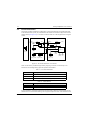
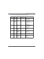
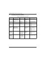
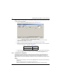
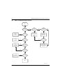
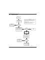
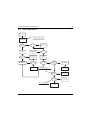
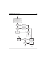
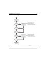
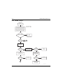
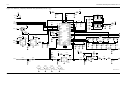
1
Note: to be printed in grayscale
SSE™ 5000
UHF Range 2
(450–488 MHz)
Portable Radio
Service Manual
SSE™ 5000
Title Page
UHF Range 2 (450–488 MHz)
Portable Radio
Service Manual
Motorola, Inc.
8000 West Sunrise Boulevard
Fort Lauderdale, Florida 33322
6881094C12-A
Foreword
This manual includes all the information necessary to maintain peak product performance and maximum working time of
the SSE 5000 portable radio, using Level 1, 2, and 3 service procedures. (For a description of the different levels of service,
see Section 3.1: “Levels of Service” on page 3-1.) Therefore, the manual contains sections on radio specifications for UHF
Range 2 (450–488 MHz), a general description of the SSE 5000 radio, radio alignment procedures, test equipment, service
aids, general maintenance recommendations, procedures for assembly and disassembly, schematics, board overlays,
parts lists, and service procedures down to the component level.
For information on user operation of the radio, refer to the applicable publications available separately (see “Related
Publications” on page vii).
Product Safety and RF Exposure Compliance
!
Caution
Before using this product, read the operating instructions
for safe usage contained in the Product Safety and RF
Exposure booklet enclosed with your radio.
ATTENTION!
This radio is restricted to occupational use only to satisfy FCC RF energy exposure requirements.
Before using this product, read the RF energy awareness information and operating instructions in the
Product Safety and RF Exposure booklet enclosed with your radio (Motorola Publication part number
6881095C98) to ensure compliance with RF energy exposure limits.
Manual Revisions
Changes which occur after this manual is printed are described in FMRs (Florida Manual Revisions). These FMRs provide
complete replacement pages for all added, changed, and deleted items. To obtain FMRs, contact the Radio Products
Services Division (refer to Appendix B: “Replacement Parts Ordering”).
Computer Software Copyrights
The Motorola products described in this manual may include copyrighted Motorola computer programs stored in
semiconductor memories or other media. Laws in the United States and other countries preserve for Motorola certain
exclusive rights for copyrighted computer programs, including, but not limited to, the exclusive right to copy or reproduce in
any form the copyrighted computer program. Accordingly, any copyrighted Motorola computer programs contained in the
Motorola products described in this manual may not be copied, reproduced, modified, reverse-engineered, or distributed in
any manner without the express written permission of Motorola. Furthermore, the purchase of Motorola products shall not
be deemed to grant either directly or by implication, estoppel, or otherwise, any license under the copyrights, patents or
patent applications of Motorola, except for the normal non-exclusive license to use that arises by operation of law in the
sale of a product.
Document Copyrights
No duplication or distribution of this document or any portion thereof shall take place without the express written permission
of Motorola. No part of this manual may be reproduced, distributed, or transmitted in any form or by any means, electronic
or mechanical, for any purpose without the express written permission of Motorola.
Disclaimer
The information in this document is carefully examined, and is believed to be entirely reliable. However, no responsibility is
assumed for inaccuracies. Furthermore, Motorola reserves the right to make changes to any products herein to improve
readability, function, or design. Motorola does not assume any liability arising out of the applications or use of any product
or circuit described herein; nor does it cover any license under its patent rights nor the rights of others.
Trademarks
MOTOROLA, the Stylized M logo, and FLASHport are registered in the US Patent & Trademark Office. All other products or
service names are the property of their respective owners.
© Motorola, Inc. 2005.
Table of Contents
iii
Table of Contents
Foreword .........................................................................................................ii
Product Safety and RF Exposure Compliance ............................................................................................ii
Manual Revisions ........................................................................................................................................ii
Computer Software Copyrights ...................................................................................................................ii
Document Copyrights ..................................................................................................................................ii
Disclaimer....................................................................................................................................................ii
Trademarks .................................................................................................................................................ii
Commercial Warranty ...................................................................................xi
Special Note on NYPD Warranty Agreement .............................................................................................xi
Limited Warranty ........................................................................................................................................xi
MOTOROLA COMMUNICATION PRODUCTS ................................................................................xi
I. What This Warranty Covers And For How Long .....................................................................xi
II. General Provisions ................................................................................................................ xii
III. State Law Rights .................................................................................................................. xii
IV. How To Get Warranty Service ............................................................................................. xii
V. What This Warranty Does Not Cover.................................................................................... xii
VI. Patent And Software Provisions ......................................................................................... xiii
VII. Governing Law................................................................................................................... xiii
Chapter 1
1.1
1.2
1.3
1.4
1.5
1.6
Physical Features of the Radio...................................................................................................... 1-1
FLASHport® ................................................................................................................................... 1-1
Portable Radio Model Numbering System..................................................................................... 1-2
SSE 5000 UHF Range 2 (450–488 MHz) Model Chart ................................................................. 1-3
Specifications for UHF Range 2 (450–488 MHz) Radios .............................................................. 1-4
Notations Used in This Manual...................................................................................................... 1-5
Chapter 2
2.1
2.2
2.3
2.4
Radio Description ............................................................... 1-1
Theory of Operation............................................................ 2-1
Major Assemblies .......................................................................................................................... 2-1
Mode of Operation ......................................................................................................................... 2-2
2.2.1 Receiving .......................................................................................................................... 2-2
2.2.2 Transmitting ...................................................................................................................... 2-3
Power Distribution.......................................................................................................................... 2-4
2.3.1 DC Power Routing—Transceiver Board ........................................................................... 2-5
2.3.2 DC Power Routing—VOCON Board................................................................................. 2-5
Transceiver Board ......................................................................................................................... 2-7
2.4.1 Interconnections ............................................................................................................... 2-7
2.4.1.1 Battery Connector J3 ............................................................................................... 2-7
2.4.1.2 VOCON Connector P1............................................................................................. 2-7
2.4.1.3 Antenna Ports .......................................................................................................... 2-8
2.4.1.4 Serial EEPROM ....................................................................................................... 2-8
2.4.1.5 Power Conditioning Components ............................................................................ 2-9
6881094C12-A
November 11, 2004
iv
Table of Contents
2.5
2.4.2 Receiver............................................................................................................................ 2-9
2.4.2.1 Receiver Front-End.................................................................................................. 2-9
2.4.2.2 Receiver Back-End ................................................................................................ 2-10
2.4.3 Transmitter...................................................................................................................... 2-11
2.4.3.1 Power Distribution.................................................................................................. 2-12
2.4.3.2 Driver Amplifier ...................................................................................................... 2-12
2.4.3.3 Power Amplifier Transistor Q107 ........................................................................... 2-12
2.4.3.4 Directional Coupler ................................................................................................ 2-13
2.4.3.5 Antenna Switch ...................................................................................................... 2-13
2.4.3.6 Harmonic Filter....................................................................................................... 2-13
2.4.3.7 RF Detector D101 .................................................................................................. 2-14
2.4.3.8 Power-Control IC (PCIC) U104.............................................................................. 2-14
2.4.4 Frequency Generation Unit (FGU) .................................................................................. 2-16
2.4.4.1 Reference Oscillator Y200 ..................................................................................... 2-16
2.4.4.2 Fractional-N Frequency Synthesizer (FracN) IC U202 .......................................... 2-16
2.4.4.3 Loop Filter .............................................................................................................. 2-17
2.4.4.4 VCO Buffer IC (VCOBIC)....................................................................................... 2-17
VOCON Board ............................................................................................................................. 2-17
2.5.1 Interconnections.............................................................................................................. 2-18
2.5.1.1 Transceiver Board Connector P201....................................................................... 2-18
2.5.1.2 Universal Flex Connector J102.............................................................................. 2-18
2.5.1.3 Internal Speaker and Microphone Flex Connector M102 ...................................... 2-19
2.5.1.4 Control Top Flex Connector J707 .......................................................................... 2-19
2.5.1.5 Encryption Module Connector J701....................................................................... 2-19
2.5.1.6 Display Module Connector J301 ............................................................................ 2-19
2.5.2 Functional Blocks............................................................................................................ 2-19
2.5.2.1 Controller and Memory .......................................................................................... 2-19
2.5.2.2 Audio and Power.................................................................................................... 2-23
2.5.2.3 Interface Support ................................................................................................... 2-26
2.5.3 Display Module ............................................................................................................... 2-31
2.5.4 Controls and Control Top Flex ........................................................................................ 2-31
2.5.5 VOCON Audio Paths ...................................................................................................... 2-32
2.5.5.1 Transmit Audio Path .............................................................................................. 2-32
2.5.5.2 Receive Audio Path ............................................................................................... 2-33
2.5.6 Radio Power-Up/Power-Down Sequence ....................................................................... 2-34
Chapter 3
3.1
3.2
3.3
3.4
Levels of Service............................................................................................................................ 3-1
Test Equipment.............................................................................................................................. 3-1
Service Aids ................................................................................................................................... 3-3
Field Programming......................................................................................................................... 3-6
Chapter 4
4.1
4.2
4.3
4.4
Test Equipment and Service Aids ..................................... 3-1
Performance Checks .......................................................... 4-1
Test Equipment Setup ................................................................................................................... 4-1
Radio Test Mode............................................................................................................................ 4-2
4.2.1 Access the Test Mode ...................................................................................................... 4-2
4.2.2 RF Test Mode ................................................................................................................... 4-4
4.2.3 Control Top Test Mode ..................................................................................................... 4-5
Receiver Performance Checks ...................................................................................................... 4-6
Transmitter Performance Checks .................................................................................................. 4-7
November 11, 2004
6881094C12-A
Table of Contents
Chapter 5
5.1
5.2
5.3
5.4
5.5
5.6
7.2
7.3
7.4
7.5
7.6
Encryption ........................................................................... 6-1
Load an Encryption Key................................................................................................................. 6-1
Multikey Feature ............................................................................................................................ 6-1
Chapter 7
7.1
Radio Alignment Procedures............................................. 5-1
Radio Alignment Test Setup .......................................................................................................... 5-1
Reading the Radio ......................................................................................................................... 5-2
Tuner Menu ................................................................................................................................... 5-2
Radio Information .......................................................................................................................... 5-2
Transmitter Alignments.................................................................................................................. 5-3
5.5.1 Softpot .............................................................................................................................. 5-3
5.5.2 Reference Oscillator Alignment ........................................................................................ 5-3
5.5.3 Transmit Power Alignment................................................................................................ 5-4
5.5.4 Transmit Deviation Balance Alignment ............................................................................. 5-7
5.5.5 Transmit Deviation Limit Alignment .................................................................................. 5-8
Performance Testing ..................................................................................................................... 5-9
5.6.1 Transmitter Test Pattern ................................................................................................... 5-9
5.6.2 Battery Reading Calibration .............................................................................................. 5-9
Chapter 6
6.1
6.2
v
Disassembly/Reassembly Procedures ............................. 7-1
General Maintenance .................................................................................................................... 7-1
7.1.1 Inspection ......................................................................................................................... 7-1
7.1.2 Cleaning............................................................................................................................ 7-1
Handling Precautions..................................................................................................................... 7-2
SSE 5000 Exploded View.............................................................................................................. 7-3
Disassembly/Reassembly Procedures for Accessories................................................................. 7-6
7.4.1 Antenna ............................................................................................................................ 7-6
7.4.1.1 Attach the Antenna .................................................................................................. 7-6
7.4.1.2 Remove the Antenna ............................................................................................... 7-6
7.4.2 Battery .............................................................................................................................. 7-6
7.4.2.1 Attach the Battery .................................................................................................... 7-7
7.4.2.2 Remove the Battery ................................................................................................. 7-7
7.4.3 Belt Clip ............................................................................................................................ 7-7
7.4.3.1 Attach the Belt Clip .................................................................................................. 7-7
7.4.3.2 Remove the Belt Clip ............................................................................................... 7-8
7.4.4 Carry Case........................................................................................................................ 7-9
7.4.5 Universal Connector Dust Cover .................................................................................... 7-10
7.4.5.1 Remove the Universal Connector Dust Cover....................................................... 7-10
7.4.5.2 Attach the Universal Connector Dust Cover .......................................................... 7-10
Disassembly/Reassembly Procedures for Radio Knobs ............................................................. 7-10
7.5.1 Channel Select Knob ...................................................................................................... 7-11
7.5.1.1 Remove the Channel Select Knob......................................................................... 7-11
7.5.1.2 Install the Channel Select Knob............................................................................. 7-11
7.5.2 Volume Knob .................................................................................................................. 7-11
7.5.2.1 Remove the Volume Knob..................................................................................... 7-11
7.5.2.2 Install the Volume Knob......................................................................................... 7-12
Disassembly Procedures for SSE 5000 Radio ............................................................................ 7-12
7.6.1 Separate the Chassis and Housing Assemblies ............................................................. 7-12
7.6.2 Disassemble the Chassis Assembly ............................................................................... 7-12
6881094C12-A
November 11, 2004
vi
Table of Contents
7.7
7.6.3 Disassemble the Control Top.......................................................................................... 7-13
7.6.4 Disassemble the Housing Baseplate .............................................................................. 7-14
Reassembly Procedures for SSE 5000 Radio ............................................................................. 7-15
7.7.1 Reassemble the Control Top .......................................................................................... 7-15
7.7.2 Reassemble the Chassis Assembly................................................................................ 7-16
7.7.3 Join the Chassis and Housing Assemblies ..................................................................... 7-16
7.7.4 Reassemble the Housing Baseplate............................................................................... 7-17
Chapter 8
8.1
8.2
8.3
8.4
8.5
8.6
8.7
Voltage Measurement and Signal Tracing..................................................................................... 8-1
Standard Bias Table ...................................................................................................................... 8-1
Power-Up Error Codes................................................................................................................... 8-2
Operational Error Codes ................................................................................................................ 8-3
Receiver Troubleshooting .............................................................................................................. 8-3
Transmitter Troubleshooting .......................................................................................................... 8-4
Encryption Troubleshooting ........................................................................................................... 8-4
Chapter 9
9.1
9.2
9.6
9.7
9.8
9.9
9.10
9.15
9.16
Troubleshooting.................................................................. 8-1
Troubleshooting Charts ..................................................... 9-1
List of Troubleshooting Charts ....................................................................................................... 9-1
Main Troubleshooting Flowchart.................................................................................................... 9-2
Volume Set Error ......................................................................................................................... 9-11
Channel Select Error.................................................................................................................... 9-12
Button Test................................................................................................................................... 9-13
Top/Side Button Test ................................................................................................................... 9-14
VCO TX/RX Unlock...................................................................................................................... 9-15
Keyload Failure ............................................................................................................................ 9-28
Secure Hardware Failure ............................................................................................................. 9-29
Chapter 10
Troubleshooting Tables ................................................... 10-1
10.1 List of Board and IC Signals ........................................................................................................ 10-1
Chapter 11
11.1
11.2
11.3
11.4
11.5
11.6
11.7
11.8
Troubleshooting Waveforms ........................................... 11-1
List of Waveforms ........................................................................................................................ 11-1
13 MHz Clock............................................................................................................................... 11-2
16.8 MHz Buffer Input and Output ............................................................................................... 11-3
32.768 kHz Clock Outputs ........................................................................................................... 11-4
SPI B Data ................................................................................................................................... 11-5
Receive Serial Audio Port (SAP) ................................................................................................. 11-6
Receive Baseband Interface Port (RX BBP)................................................................................ 11-7
Transmit Baseband Interface Port (TX BBP) ............................................................................... 11-8
Chapter 12
Schematics, Board Layouts, and Parts Lists ................. 12-1
12.1 Transceiver (RF) Board ............................................................................................................... 12-2
12.2 VOCON Board ........................................................................................................................... 12-17
November 11, 2004
6881094C12-A
Table of Contents
vii
12.3 Control Flex ............................................................................................................................... 12-33
12.4 Universal Flex ............................................................................................................................ 12-35
12.5 UCM........................................................................................................................................... 12-37
Appendix A Accessories .........................................................................A-1
A.1
A.2
A.3
A.4
A.5
A.6
A.7
A.8
A.9
Antennas........................................................................................................................................A-1
Batteries.........................................................................................................................................A-1
Carrying Accessories.....................................................................................................................A-1
Chargers and Charger Accessories...............................................................................................A-1
Dust Cover.....................................................................................................................................A-1
Keyload Accessories .....................................................................................................................A-2
Microphones and Microphone Accessories ...................................................................................A-2
Programming Cables .....................................................................................................................A-2
Surveillance Accessories...............................................................................................................A-2
Appendix B Replacement Parts Ordering..............................................B-1
B.1
B.2
B.3
B.4
B.5
B.6
B.7
B.8
Basic Ordering Information ............................................................................................................B-1
Transceiver Board and VOCON Board Ordering Information........................................................B-1
Motorola Online .............................................................................................................................B-1
Mail Orders ....................................................................................................................................B-1
Telephone Orders..........................................................................................................................B-1
Fax Orders.....................................................................................................................................B-2
Parts Identification .........................................................................................................................B-2
Product Customer Service.............................................................................................................B-2
Glossary ......................................................................................... Glossary-1
Index ..................................................................................................... Index-1
Related Publications
SSE 5000 Portable Radio User Guide....................................................................................... 6881094C11
SSE 5000 Portable Radio User Guide (on CD) ......................................................................... 9985086F04
SSE 5000 Product Listing (Factory Mutual Approval) ............................................................... 6881094C14
SSE 5000 Portable Radio Quick Guide ..................................................................................... 6881094C16
SSE 5000 Interactive End-User Training (on CD) ..................................................................... 6881094C17
SSE 5000 Portable Radio Service Manual (on CD) .................................................................. 9985086F05
FLASHport User Guide.............................................................................................................. 6881094C35
CPS Installation guide ............................................................................................................... 6881095C44
6881094C12-A
November 11, 2004
viii
Notes
November 11, 2004
6881094C12-A
List of Figures
ix
List of Figures
Figure 1-1. Physical Features of the SSE 5000 Radio............................................................................ 1-1
Figure 2-1. SSE 5000 Overall Block Diagram ......................................................................................... 2-1
Figure 2-2. Receiver Block Diagram ....................................................................................................... 2-2
Figure 2-3. Transceiver (UHF Range) Block Diagram (Power and Control Omitted).............................. 2-3
Figure 2-4. DC Power Distribution—UHF Radios ................................................................................... 2-4
Figure 2-5. Abacus III (AD9874) Functional Block Diagram.................................................................. 2-11
Figure 2-6. Transmitter Block Diagram ................................................................................................. 2-12
Figure 2-7. VOCON Board Block Diagram............................................................................................ 2-18
Figure 2-8. Dual-Core Processor EIM and Memory Block Diagram...................................................... 2-23
Figure 2-9. Universal Side Connector ................................................................................................... 2-29
Figure 2-10. VOCON Board Connector J102.......................................................................................... 2-30
Figure 2-11. VOCON Transmit Audio Path ............................................................................................. 2-33
Figure 2-12. VOCON Receive Audio Path .............................................................................................. 2-34
Figure 4-1. Performance Checks Test Setup .......................................................................................... 4-1
Figure 5-1. Radio Alignment Test Setup.................................................................................................. 5-1
Figure 5-2. Tuner Software Main Menu................................................................................................... 5-2
Figure 5-3. Radio Information Screen ..................................................................................................... 5-2
Figure 5-4. Typical Softpot Screen .......................................................................................................... 5-3
Figure 5-5. Reference Oscillator Alignment Screen ................................................................................ 5-4
Figure 5-6. Transmit Power Alignment Screen (High Power) ................................................................. 5-6
Figure 5-7. Transmit Power Alignment Screen (Low Power) .................................................................. 5-6
Figure 5-8. Transmit Deviation Balance Alignment Screen..................................................................... 5-7
Figure 5-9. Transmit Deviation Limit Alignment Screen .......................................................................... 5-8
Figure 5-10. Transmitter Test Pattern Screen ........................................................................................... 5-9
Figure 5-11. Battery Reading Calibration Screen.................................................................................... 5-10
Figure 7-1. SSE 5000 Exploded View ..................................................................................................... 7-3
Figure 7-2. Attaching/Removing the Antenna ......................................................................................... 7-6
Figure 7-3. Attaching/Removing the Battery ........................................................................................... 7-7
Figure 7-4. Attaching the Belt Clip........................................................................................................... 7-8
Figure 7-5. Removing the Belt Clip ......................................................................................................... 7-8
Figure 7-6. Assembling the Carry Case .................................................................................................. 7-9
Figure 7-7. Attaching the Universal Connector Dust Cover .................................................................. 7-10
Figure 11-1. 13 MHz Clock Waveform .................................................................................................... 11-2
Figure 11-2. 16.8 MHz Buffer Input and Output Waveforms ................................................................... 11-3
Figure 11-3. 32.768 kHz Clock Outputs Waveforms ............................................................................... 11-4
Figure 11-4. SPI B Data Waveforms ....................................................................................................... 11-5
Figure 11-5. Receive Serial Audio Port (SAP) Waveforms ..................................................................... 11-6
Figure 11-6. Receive Baseband Interface Port (RX BBP) Waveforms ................................................... 11-7
Figure 11-7. Transmit Baseband Interface Port (TX BBP) Waveforms ................................................... 11-8
6881094C12-A
November 11, 2004
x
List of Tables
List of Tables
Table 2-1.
Table 2-2.
Table 2-3.
Table 2-4.
Table 2-5.
Table 2-6.
Table 2-7.
Table 2-8.
Table 2-9.
Table 2-10.
Table 2-11.
Table 3-1.
Table 3-2.
Table 4-1.
Table 4-2.
Table 4-3.
Table 4-4.
Table 4-5.
Table 4-6.
Table 5-1.
Table 5-2.
Table 7-1.
Table 7-2.
Table 8-1.
Table 8-2.
Table 8-3.
Table 8-4.
Table 8-5.
Table 8-6.
Table 9-1.
Table 10-1.
Table 10-2.
Table 10-3.
Table 10-4.
Table 10-5.
Table 10-6.
Table 10-7.
Table 10-8.
Table 10-9.
Table 11-1.
Table 12-1.
Table 12-2.
Table 12-3.
Table 12-4.
Table 12-5.
Conventional Batteries .......................................................................................................... 2-4
Smart Batteries ..................................................................................................................... 2-4
Transceiver Voltage Regulators ............................................................................................ 2-5
VOCON Board DC Power Distribution .................................................................................. 2-6
Battery Connector J3 ............................................................................................................ 2-7
VOCON Connector P1 .......................................................................................................... 2-7
Local Oscillator and First IF Frequencies ............................................................................. 2-9
Power Control IC (U104) Pin Descriptions.......................................................................... 2-14
Audio PA Status .................................................................................................................. 2-26
Pin Assignments for Universal Side Connector .................................................................. 2-30
Option Select Functions ...................................................................................................... 2-31
Test Equipment ..................................................................................................................... 3-1
Service Aids .......................................................................................................................... 3-3
Initial Equipment Control Settings ......................................................................................... 4-2
Test-Mode Displays............................................................................................................... 4-3
Test Frequencies (MHz) ........................................................................................................ 4-4
Test Environments................................................................................................................. 4-4
Receiver Performance Checks ............................................................................................. 4-6
Transmitter Performance Checks ......................................................................................... 4-7
Reference Oscillator Alignment ............................................................................................ 5-4
Transmit Power Settings ....................................................................................................... 5-5
SSE 5000 Exploded View Parts List ..................................................................................... 7-4
Tools Used for Disassembly/Reassembly ........................................................................... 7-10
Standard Operating Bias ....................................................................................................... 8-1
Power-Up Error Code Displays ............................................................................................. 8-2
Operational Error Code Displays .......................................................................................... 8-3
Receiver Troubleshooting Chart ........................................................................................... 8-3
Transmitter Troubleshooting Chart........................................................................................ 8-4
Encryption Troubleshooting Chart......................................................................................... 8-4
Troubleshooting Charts List .................................................................................................. 9-1
List of Tables of Board and IC Signals ................................................................................ 10-1
J102 VOCON Board to Universal Flex................................................................................ 10-2
J707 VOCON Board to Controls Flex Assembly................................................................. 10-2
J701 VOCON Board to Encryption Module......................................................................... 10-3
U402 FLASH Pinouts .......................................................................................................... 10-4
U403 SRAM Pinouts ........................................................................................................... 10-6
U401 MCU/DSP IC Pinouts ................................................................................................ 10-8
U301 Digital-Support IC Pinouts ....................................................................................... 10-17
U501 GCAP II IC Pinouts.................................................................................................. 10-19
List of Waveforms ............................................................................................................... 11-1
List of Transceiver Schematics, Board Layouts and Parts Lists ......................................... 12-1
List of VOCON Schematics, Board Layouts and Parts Lists ............................................... 12-1
List of Control Flex Schematics and Board Layouts ........................................................... 12-1
List of Universal Flex Schematics and Board Layouts ........................................................ 12-1
List of UCM Schematics and Board Layouts....................................................................... 12-1
November 11, 2004
6881094C12-A
Commercial Warranty
Special Note on NYPD Warranty Agreement
The three-year warranty on the NYPD SSE 5000 portable radio units represents the combination of the
standard one-year product warranty (detailed in this section) and the two-year Motorola Express Service Plus
(ESP) option. ESP is an extended service coverage plan, which provides for the repair of this product for an
additional period of two years beyond the expiration date of the standard warranty. For more information about
ESP, contact the Motorola Radio Support Center at 2200 Galvin Drive, Elgin IL 60123, (800) 422-4210 (U.S.
and Canada) / (847) 538-8023 (international).
Limited Warranty
MOTOROLA COMMUNICATION PRODUCTS
I. What This Warranty Covers And For How Long
MOTOROLA INC. (“MOTOROLA”) warrants the MOTOROLA manufactured Communication
Products listed below (“Product”) against defects in material and workmanship under normal use and
service for a period of time from the date of purchase as scheduled below:
SSE 5000 Portable Units
Three (3) Years
Product Accessories
One (1) Year
Motorola, at its option, will at no charge either repair the Product (with new or reconditioned parts),
replace it (with a new or reconditioned Product), or refund the purchase price of the Product during
the warranty period provided it is returned in accordance with the terms of this warranty. Replaced
parts or boards are warranted for the balance of the original applicable warranty period. All replaced
parts of Product shall become the property of MOTOROLA.
This express limited warranty is extended by MOTOROLA to the original end user purchaser only
and is not assignable or transferable to any other party. This is the complete warranty for the Product
manufactured by MOTOROLA. MOTOROLA assumes no obligations or liability for additions or
modifications to this warranty unless made in writing and signed by an officer of MOTOROLA.
Unless made in a separate agreement between MOTOROLA and the original end user purchaser,
MOTOROLA does not warrant the installation, maintenance or service of the Product.
MOTOROLA cannot be responsible in any way for any ancillary equipment not furnished by
MOTOROLA which is attached to or used in connection with the Product, or for operation of the
Product with any ancillary equipment, and all such equipment is expressly excluded from this
warranty. Because each system which may use the Product is unique, MOTOROLA disclaims
liability for range, coverage, or operation of the system as a whole under this warranty.
xii
Commercial Warranty
II. General Provisions
This warranty sets forth the full extent of MOTOROLA’S responsibilities regarding the Product.
Repair, replacement or refund of the purchase price, at MOTOROLA’s option, is the exclusive
remedy. THIS WARRANTY IS GIVEN IN LIEU OF ALL OTHER EXPRESS WARRANTIES. IMPLIED
WARRANTIES, INCLUDING WITHOUT LIMITATION, IMPLIED WARRANTIES OF
MERCHANTABILITY AND FITNESS FOR A PARTICULAR PURPOSE, ARE LIMITED TO THE
DURATION OF THIS LIMITED WARRANTY. IN NO EVENT SHALL MOTOROLA BE LIABLE FOR
DAMAGES IN EXCESS OF THE PURCHASE PRICE OF THE PRODUCT, FOR ANY LOSS OF
USE, LOSS OF TIME, INCONVENIENCE, COMMERCIAL LOSS, LOST PROFITS OR SAVINGS
OR OTHER INCIDENTAL, SPECIAL OR CONSEQUENTIAL DAMAGES ARISING OUT OF THE
USE OR INABILITY TO USE SUCH PRODUCT, TO THE FULL EXTENT SUCH MAY BE
DISCLAIMED BY LAW.
III. State Law Rights
SOME STATES DO NOT ALLOW THE EXCLUSION OR LIMITATION OF INCIDENTAL OR
CONSEQUENTIAL DAMAGES OR LIMITATION ON HOW LONG AN IMPLIED WARRANTY
LASTS, SO THE ABOVE LIMITATION OR EXCLUSIONS MAY NOT APPLY.
This warranty gives specific legal rights, and there may be other rights which may vary from state to
state.
IV. How To Get Warranty Service
You must provide proof of purchase (bearing the date of purchase and Product item serial number)
in order to receive warranty service and, also, deliver or send the Product item, transportation and
insurance prepaid, to an authorized warranty service location. Warranty service will be provided by
Motorola through one of its authorized warranty service locations. If you first contact the company
which sold you the Product, it can facilitate your obtaining warranty service. You can also call
Motorola at 1-888-567-7347 US/Canada.
V. What This Warranty Does Not Cover
A. Defects or damage resulting from use of the Product in other than its normal and customary
manner.
B. Defects or damage from misuse, accident, water, or neglect.
C. Defects or damage from improper testing, operation, maintenance, installation, alteration,
modification, or adjustment.
D. Breakage or damage to antennas unless caused directly by defects in material workmanship.
E. A Product subjected to unauthorized Product modifications, disassemblies or repairs
(including, without limitation, the addition to the Product of non-Motorola supplied equipment)
which adversely affect performance of the Product or interfere with Motorola's normal
warranty inspection and testing of the Product to verify any warranty claim.
F.
Product which has had the serial number removed or made illegible.
G. Rechargeable batteries if:
- any of the seals on the battery enclosure of cells are broken or show evidence of
tampering.
- the damage or defect is caused by charging or using the battery in equipment or service
other than the Product for which it is specified.
H. Freight costs to the repair depot.
November 11, 2004
6881094C12-A
Commercial Warranty
xiii
I.
A Product which, due to illegal or unauthorized alteration of the software/firmware in the
Product, does not function in accordance with MOTOROLA’s published specifications or the
FCC type acceptance labeling in effect for the Product at the time the Product was initially
distributed from MOTOROLA.
J.
Scratches or other cosmetic damage to Product surfaces that does not affect the operation of
the Product.
K. Normal and customary wear and tear.
VI. Patent And Software Provisions
MOTOROLA will defend, at its own expense, any suit brought against the end user purchaser to the
extent that it is based on a claim that the Product or parts infringe a United States patent, and
MOTOROLA will pay those costs and damages finally awarded against the end user purchaser in
any such suit which are attributable to any such claim, but such defense and payments are
conditioned on the following:
A. that MOTOROLA will be notified promptly in writing by such purchaser of any notice of such
claim;
B. that MOTOROLA will have sole control of the defense of such suit and all negotiations for its
settlement or compromise; and
C. should the Product or parts become, or in MOTOROLA’s opinion be likely to become, the
subject of a claim of infringement of a United States patent, that such purchaser will permit
MOTOROLA, at its option and expense, either to procure for such purchaser the right to
continue using the Product or parts or to replace or modify the same so that it becomes
noninfringing or to grant such purchaser a credit for the Product or parts as depreciated and
accept its return. The depreciation will be an equal amount per year over the lifetime of the
Product or parts as established by MOTOROLA.
MOTOROLA will have no liability with respect to any claim of patent infringement which is based
upon the combination of the Product or parts furnished hereunder with software, apparatus or
devices not furnished by MOTOROLA, nor will MOTOROLA have any liability for the use of ancillary
equipment or software not furnished by MOTOROLA which is attached to or used in connection with
the Product. The foregoing states the entire liability of MOTOROLA with respect to infringement of
patents by the Product or any parts thereof.
Laws in the United States and other countries preserve for MOTOROLA certain exclusive rights for
copyrighted MOTOROLA software such as the exclusive rights to reproduce in copies and distribute
copies of such Motorola software. MOTOROLA software may be used in only the Product in which
the software was originally embodied and such software in such Product may not be replaced,
copied, distributed, modified in any way, or used to produce any derivative thereof. No other use
including, without limitation, alteration, modification, reproduction, distribution, or reverse
engineering of such MOTOROLA software or exercise of rights in such MOTOROLA software is
permitted. No license is granted by implication, estoppel or otherwise under MOTOROLA patent
rights or copyrights.
VII. Governing Law
This Warranty is governed by the laws of the State of Illinois, USA.
6881094C12-A
November 11, 2004
xiv
Commercial Warranty
Notes
November 11, 2004
6881094C12-A
Chapter 1 Radio Description
1.1
Physical Features of the Radio
Figure 1-1 shows the physical features of the SSE 5000 portable radio.
Display
Button
Monitor
Button
15
Control
Top
1
7
5
Channel
Bank Select
Switch
Transmit/
Receive
Indicator
(LED)
3
On/Off/
Volume
Knob
Antenna
Channel
Select
Knob
SS
NY
000
E5
Display (1 line x 8 char,
bitmapped LCD)
PD
Speaker/
Mic
PTT
Channel
Bank
Button
Secure
Button
Battery
Figure 1-1. Physical Features of the SSE 5000 Radio
The SSE 5000 portable radio operates in the UHF Range 2 (450–488 MHz) frequency band. It can
be programmed with up to 96 channels. Earlier versions of the radio, which could be programmed
with up to 48 channels, can be upgraded to 96-channel capability via FLASHport®.
1.2
FLASHport®
The SSE 5000 radio utilizes Motorola’s FLASHport technology. FLASHport allows you to add
software that drives the radio’s capabilities, both at the time of purchase and afterwards. Previously,
changing a radio’s features and capabilities meant significant modifications, or buying a new radio.
Now the radio’s features and capabilities can be upgraded with FLASHport software, similar to how a
computer can be loaded with different software. For information on upgrading the radio’s features
using FLASHport, see the FLASHport User Guide (Motorola publication part number 6881094C35).
1-2
1.3
Radio Description: Portable Radio Model Numbering System
Portable Radio Model Numbering System
SSE 5000 Model Number: H 1 0
Position: 1 2 3
S
4
D D
5 6
Position 1 - Type of Unit
H = Hand-Held Portable
P
8
W 6
9 10
A
11
N S P 0 1
12 13 14 15 16
Positions 13 - 16
SP Model Suffix
Position 12 - Unique Model Variations
C = Cenelec
N = Standard Package
Positions 2 & 3 - Model Series
10 = SSE 5000
Position 4 - Frequency Band
A = Less than 29.7MHz
P=
B = 29.7 to 35.99MHz
Q=
C = 36 to 41.99MHz
R=
D = 42 to 50MHz
S=
F = 66 to 80MHz
T=
G = 74 to 90MHz
U=
H = Product Specific
V=
J = 136 to 162MHz
W=
K = 146 to 178MHz
Y=
L = 174 to 210MHz
Z=
M = 190 to 235MHz
9
7
336 to 410MHz
403 to 437MHz
438 to 482MHz
470 to 520MHz
Product Specific
764 to 870MHz
825 to 870MHz
896 to 941MHz
1.0 to 1.6GHz
1.5 to 2.0GHz
Values given represent range only; they are
not absolute.
Position 5 - Power Level
A = 0 to 0.7 Watts
B = 0.7 to 0.9 Watts
C = 1.0 to 3.9 Watts
D = 4.0 to 5.0 Watts
E = 5.1 to 6.0 Watts
F = 6.1 to 10 Watts
Position 6 - Physical Packages
A = RF Modem Operation
B = Receiver Only
C = Standard Control; No Display
D = Standard Control; With Display
E = Limited Keypad; No Display
F = Limited Keypad; With Display
G = Full Keypad; No Display
H = Full Keypad; With Display
J = Limited Controls; No Display
K = Limited Controls; Basic Display
L = Limited Controls; Limited Display
M = Rotary Controls; Standard Display
N = Enhanced Controls; Enhanced Display
P = Low Profile; No Display
Q = Low Profile; Basic Display
R = Low Profile; Basic Display, Full Keypad
Position 7 - Channel Spacing
1 = 5kHz
5 = 15kHz
2 = 6.25kHz 6 = 20/25kHz
3 = 10kHz 7 = 30kHz
4 = 12.5kHz 9 = Variable/Programmable
Position 11 - Version
Version Letter (Alpha) - Major Change
Position 10 - Feature Level
1 = Basic
6 = Standard Plus
2 = Limited Package 7 = Expanded Package
3 = Limited Plus
8 = Expanded Plus
4 = Intermediate
9 = Full Feature/
5 = Standard Package Programmable
Position 9 - Primary System Type
A = Conventional
B = Privacy Plus
C = Clear SMARTNET
D = Advanced Conventional Stat-Alert
E = Enhanced Privacy Plus
F = Nauganet 888 Series
G = Japan Specialized Mobile Radio (JSMR)
H = Multi-Channel Access (MCA)
J = CoveragePLUS
K = MPT1327* - Public
L = MPT1327* - Private
M = Radiocom
N = Tone Signalling
P = Binary Signalling
Q = Phonenet
W = Programmable
X = Secure Conventional
Y = Secure SMARTNET
* MPT = Ministry of Posts and Telecommunications
Position 8 - Primary Operation
A = Conventional/Simplex
B = Conventional/Duplex
C = Trunked Twin Type
D = Dual Mode Trunked
E = Dual Mode Trunked/Duplex
F = Trunked Type I
G = Trunked Type II
H = FDMA* Digital Dual Mode
J = TDMA** Digital Dual Mode
K = Single Sideband
L = Global Positioning Satellite Capable
M = Amplitude Companded Sideband (ACSB)
P = Programmable
* FDMA = Frequency Division Multiple Access
** TDMA = Time Division Multiple Access
MAEPF-27326-A
November 11, 2004
6881094C12-A
Radio Description: SSE 5000 UHF Range 2 (450–488 MHz) Model Chart
1.4
1-3
SSE 5000 UHF Range 2 (450–488 MHz) Model Chart
MODEL NUMBER
H10SDD9PW6AN
ITEM NUMBER
X
—
X
—
X
NUE7337_
X
NCN6186_
X
—
X
—
X
—
X
NTN7061_
X
NNTN4709_
X
NNTN4825_
X
NNTN4826_
X
8485687E01
X
NNTN4468_
X
NNTN4467_
X
8485791E01
X
—
X
NNTN4006_
XX —
DESCRIPTION
UHF Range 2 (450–488 MHz), 2–5 Watts, SSE 5000
DESCRIPTION
Antenna, UHF (Refer to Section A.1: “Antennas” on page A-1)
Battery (Refer to Section A.2: “Batteries” on page A-1)
Board, Transceiver, UHF Range 2 (450–488 MHz)
Board, VOCON *
Cable, Programming (Refer to Section A.8: “Programming Cables” on page A-2)
Case, Carrying (Refer to Section A.3: “Carrying Accessories” on page A-1)
Charger (Refer to Section A.4: “Chargers and Charger Accessories” on page A-1)
Cover, Accessory Connector
Kit, Belt Clip
Kit, Chassis, Back
Kit, Chassis, Front
Kit, Control Flex
Kit, Hardware
Kit, Housing
Kit, Speaker Mic Flex
Mic Accessories (Refer to Section A.7: “Microphones and Microphone Accessories” on page A-2)
Module, Encryption, DES, DES-XL, DES-PFB
Surveillance Accessories (Refer to Section A.9: “Surveillance Accessories” on page A-2)
Notes:
X = Item Included
* = When ordering a VOCON board, you will be asked to provide the radio's model number, FLASHcode, host
code, and DSP code. You can find this information as follows:
• For the radio model number and FLASHcode, place the radio in test mode (see Section 4.2: “Radio Test
Mode” on page 4-2) and view the scrolling displays.
• For the host code and DSP code, read the radio using the programming cable (RKN4121_ or RKN4122_)
and view the information in the CPS.
6881094C12-A
November 11, 2004
1-4
1.5
Radio Description: Specifications for UHF Range 2 (450–488 MHz) Radios
Specifications for UHF Range 2 (450–488 MHz) Radios
All specifications are per Telecommunications Industry Association TIA/EIA-603 unless otherwise
noted.
GENERAL
FCC Designation:
Temperature Range:
Operating:
Storage:
RECEIVER
AZ489FT4861
–30°C to +60°C
–40°C to +85°C
Power Supply: Nickel-Cadmium Battery (NiCd)
Battery Voltage:
Nominal:
Range:
Frequency Range:
TRANSMITTER
450–488 MHz
Bandwidth:
38 MHz
Reference Sensitivity (12 dB SINAD) (typical):
0.25 µV
Intermodulation Rejection (typical):
7.5 Vdc
6 to 9 Vdc
Transmit Current Drain (typical)*:
5W RF Power:
1800 mA
2W RF Power:
1100 mA
Receive Current Drain at Rated Audio
(typical)*:
240 mA
Standby Current Drain (typical)*:
80 mA
Frequency Range:
Conducted Carrier Output Power Rating:
450–488 MHz:
2–5 Watts
Carrier Frequency Stability (typical)
(–30 to +60°C; 25°C ref.):
±0.0002%
75 dB
Adjacent Channel Rejection (typical):
25/30 kHz 78 dB
12.5 kHz 68 dB
Spurious Response Rejection (typical): 80 dB
Rated Audio Frequency Output Power:
500 mW
Conducted Spurious Emissions (typical):
70 dBc
FM Hum and Noise Ratio (typical)
(Companion Receiver):
25 kHz 50 dB
12.5 kHz 40 dB
Audio Distortion (typical):
Modulation Limiting:
Recommended Battery:
NiCd:
NTN4595
or NiCd Smart:
HNN9033
Optional FM (Factory Mutual) Battery:
NiCd FM:
NTN4596*
or NiCd FM (HazMat):
NTN4992*
or NiCd Smart FM:
HNN9034*
* FM Intrinsically Safe.
Hum and Noise Ratio (typical):
25 kHz 50 dB
12.5 kHz 43 dB
Audio Distortion (typical):
Channel Spacing:
450–488 MHz
1.0%
12.5/25 kHz
1.5%
25 kHz ±5.0 kHz
12.5 kHz ±2.5 kHz
Adjacent Channel Power Ratio (ACPR)
(typical):
25 kHz 77 dBc
12.5 kHz 62 dBc
Emissions Designators:
20K0F1E, 16K0F3E, 11K0F3E, 8K10F1D, and
8K10F1E
Dimensions (H x W x D):
Without Battery (Radio Only):
D
H
W
(no antenna) (at cntl top)
(at cntl top)
4.7 in.
2.92 in.
1.37 in.
119.5 mm
74.2 mm
34.9 mm
(no antenna) (at bottom)
(at PTT)
4.7 in.
2.66 in.
1.27 in.
119.5 mm
67.6 mm
32.2 mm
With Battery:
D
H
W
(no antenna) (at cntl top)
(at cntl top)
8.5 in.
2.92 in.
1.37 in.
215.9 mm
74.2 mm
34.9 mm
(no antenna) (at bottom)
(at PTT)
8.5 in.
2.66 in.
1.27 in.
215.9 mm
67.6 mm
32.2 mm
Weight: (w/ Antenna):
Less Battery:
With NiCd Smart:
With NiCd:
11.2 oz (316.9 gm)
15.9 oz (449.4 gm)
13.7 oz (387.8 gm)
* Test box will add 25 mA.
Specifications subject to change without notice.
November 11, 2004
6881094C12-A
Radio Description: Notations Used in This Manual
1.6
1-5
Notations Used in This Manual
Throughout the text in this publication, you will notice the use of note, caution, warning, and danger
notations. These notations are used to emphasize that safety hazards exist, and due care must be
taken and observed.
NOTE: An operational procedure, practice, or condition that is essential to emphasize.
!
CAUTION indicates a potentially hazardous situation which, if
not avoided, might result in equipment damage.
Caution
!
WARNING
!
DANGER
6881094C12-A
WARNING indicates a potentially hazardous situation
which, if not avoided, could result in death or injury.
DANGER indicates an imminently hazardous
situation which, if not avoided, will result in death or
injury.
November 11, 2004
1-6
Radio Description: Notations Used in This Manual
Notes
November 11, 2004
6881094C12-A
Chapter 2 Theory of Operation
This chapter provides a detailed circuit description of the SSE 5000 transceiver and VOCON boards.
When reading the theory of operation, refer to the appropriate schematic and component location
diagrams located in the back of this manual. This detailed theory of operation can help isolate the
problem to a particular component.
The SSE 5000 radio is a dual-mode (digital/analog), microcontroller-based transceiver incorporating
a digital signal processor (DSP). The microcontroller handles the general radio control, monitors
status, and processes commands input from the keypad or other user controls. The DSP processes
the typical analog signals, and generates the standard signaling digitally to provide compatibility with
existing analog systems. In addition, the DSP provides digital modulation techniques, utilizing voice
encoding techniques with error correction schemes. This provides the user with enhanced range and
audio quality, all in a reduced bandwidth channel requirement. It allows embedded signaling, which
can mix system information and data with digital voice to support a multitude of system features.
The SSE 5000 radio operates within the UHF range (450 to 488 MHz).
2.1
Major Assemblies
The SSE 5000 radio includes the following major assemblies (see Figure 2-1):
• VOCON Board — contains a dual-core processor which includes both the microcontroller unit
(MCU) and a digital signal processor (DSP) core, the processor’s memory devices, an audio
and power supply support integrated circuit (IC), a digital-support IC, and the audio power
amplifier.
• Transceiver (XCVR) Board — contains all transmit, receive, and frequency generation
circuitry, including the digital receiver back-end IC and the reference oscillator.
• Controls/Universal Flex — contains on/off/volume switch, channel select switch, push-to-talk
(PTT) switch, monitor button, several function-selectable switches, universal connector,
speaker, and microphone.
• Display — 112 pixels x 32 pixels bit-mapped, liquid-crystal display (LCD).
Internal Speaker
& Mic Flex
12
Control
Top
Display
External
Accessory
Connector
7.5V
Battery
M102
P201
Note:
Indicates 12
wires
Standard
Antenna
4
20
20
26
P1
J101
Remote
Antenna
Transceiver
Board
J707
J102
VOCON
Board
J301
J1
3
12
14
3
Universal
Flex
J102
J701
40
Encryption
Module
(Optional)
MAEPF-27277-B
Figure 2-1. SSE 5000 Overall Block Diagram
2-2
2.2
Theory of Operation: Mode of Operation
Mode of Operation
This section provides an overview of the radio’s receive and transmit operation in the analog mode.
2.2.1
Receiving
When the radio is receiving (see Figure 2-2), the signal travels from the antenna connector to the
transceiver board, passing through the antenna switch and the receiver front-end. The signal is then
filtered, amplified, and mixed with the first local-oscillator signal, generated by the voltage-controlled
oscillator (VCO).
RX Front End
RF Input
Harmonic
Filter
Remote
Port
Harmonic
Filter
Antenna
Switch
Preselector
Filter
LNA
Preselector
Filter
1st LO
1st
Mixer
ABACUS III - RX Back End
XTAL
Filter
3 ADC
LO
RX_SSI_ DATA
to VOCON Board
CKO
MAEPF-27278-B
Figure 2-2. Receiver Block Diagram
The resulting intermediate frequency (IF) signal is fed to the IF circuitry, where it is again filtered and
passed to the Abacus III digital back-end IC. In the digital back-end IC, the IF signal is mixed with the
second local oscillator to create the second IF at 2.25 MHz. In the back-end IC, a bandpass, sigmadelta, analog-to-digital converter then decodes the second IF signal, and outputs, on the radio’s
serial synchronous interface (SSI) bus, digital audio to the VOCON board.
On the VOCON board, the dual-core processor’s digital-signal processor (DSP) digitally filters the
PCM audio. The DSP decodes the information in the signal and identifies the appropriate destination
for it.
• For a voice signal, the DSP will route the digital voice data to the CODEC inside the audio and
power supply support IC, for conversion to an analog signal. The CODEC will then present the
signal to the receive audio pre-amplifier, then to the audio power amplifier, which drives the
speaker.
• For signaling information, the DSP will decode the message and pass it internally to the
microcontrol unit of the dual-core processor.
November 11, 2004
6881094C12-A
Theory of Operation: Mode of Operation
2.2.2
2-3
Transmitting
When the radio is transmitting, microphone audio is passed through gain stages to the CODEC,
where the signal is digitized (see Figure 2-3). The CODEC passes digital data to the DSP, where preemphasis and low-pass (splatter) filtering are done. The DSP passes this signal to a digital/analog
converter (DAC), where it is reconverted into an analog signal and scaled for application to the
voltage-controlled oscillator as a modulation signal.
TX Driver
TX
Amplifier
VCOBIC Buffer
U102
Reference
Oscillator
Loop
Filter
Y200
Power
Module
Q107
VCO 1
FracN
Directional
Coupler
U101
D101
VCO 2
TX_SSI from
VOCON Board
3 MOD
IN
LPF
FL200
DAC
U203
Dual Antenna
Switch Note:
This UHF range has 2 VCOs (1 TX, 1 RX)
To
Remote
Port
PCIC
U104
Harmonic
Filter
Serial EE
PROM
U4
To
Antenna
ABACUS III U500
3 RX_SSI to
VOCON Board
Crystal
Filter
Sample
Clk
Mixer
Preselector RX LNA Preselector
Filter
Filter
2ND
LO
MAEPF-27530-A
Figure 2-3. Transceiver (UHF Range) Block Diagram (Power and Control Omitted)
Transmitted signaling information is applied to the DSP from the microcontrol unit, where it is coded,
and passed to the DAC, which handles it the same as a voice signal. The DAC output connects to
the synthesizer modulation input. A modulated carrier is provided to the transmitter power amplifier,
which transmits the signal under dynamic power control.
6881094C12-A
November 11, 2004
2-4
2.3
Theory of Operation: Power Distribution
Power Distribution
This section provides a detailed circuit description of the power distribution of the SSE 5000 radio.
In the SSE 5000 radio, power (B+) is distributed to two boards: the transceiver (RF) board and the
VOCON board (see Figure 2-4). In the case of a secure radio, B+ is also supplied to the encryption
module.
VOCON Board
RF Board
Battery
J1 BATT
FB+
Fuse
UNSW_B+
P1
VCC 5
P201
RAW B+
FET
FET
XB+
(control signal)
5 Volts
SW_B+
3.8 V (VSW1)
V5A
GCAP II
7.5 Volts
(Nominal)
5 Volts
V3A
V3D
1.55V
3 Volts
Analog Circuits
3 Volts
Digital Circuits
1.55 Volts
(VSW_1.55)
1.875 Volts
(VSW2)
2.893 2.893 Volts Volts
(VREF) (V2)
MAEPF-27419-A
Figure 2-4. DC Power Distribution—UHF Radios
Power for the radio is provided through a battery supplying a nominal 7.5 Vdc directly to the
transceiver. The following battery types and capacities are available:
Table 2-1. Conventional Batteries
Part Number
Description
NTN4595
Premium NiCd (1800 mAh, 7.5 V)
NTN4596
Premium NiCd FM (1800 mAh, 7.5 V)
NTN4992
Premium NiCd FM (1800 mAh, 7.5 V) (HazMat)
Table 2-2. Smart Batteries
Part Number
Description
HNN9033
impres™ NiCd (2000 mAh)
HNN9034
impres™ NiCd FM (2000 mAh)
B+ from the battery is electrically switched to most of the radio, rather than routed through the On/
Off/Volume knob. The electrical switching of B+ supports a keep-alive mode. Under software control,
November 11, 2004
6881094C12-A
Theory of Operation: Power Distribution
2-5
even when the On/Off/Volume knob has been turned to the off position, power remains on until the
microcontroller unit (MCU) completes its power-down, at which time the radio is physically powered
down.
2.3.1
DC Power Routing—Transceiver Board
Connector J1, the B+ assembly, connects the battery to the transceiver board. Two capacitors
provide protection against momentary breaks at the B+ connector due to contact bounce when the
radio is dropped.
An RF bead forms a power-line filter for signal RAWB+, which supplies battery voltage to the
transmitter PA.
A transistor, controlled by signal SWB+ from the VOCON board, turns on XB+, which supplies the
5-V linear regulator, TX_ALC block and SW_FL.
Fuse F901 and a filter supply fused B-plus to the VOCON board. In turn, the VOCON board supplies
VSW1, regulated 3.8 Vdc, from the Global Control Audio and Power (GCAP) switching regulator to
the XCVR. A switch, controlled by SWB+, turns on V38 to the XCVR 3-V linear regulators. The
XCVR regulated power supplies are summarized in Table 2-3.
Table 2-3. Transceiver Voltage Regulators
IC
Name
2.3.2
Output
Signal Name
Description
LP2989
V5A
Regulated 5.0 Vdc
LP3985
V3D
Regulated 3.0 Vdc digital
LP3985
V3A
Regulated 3.0 Vdc analog for the RX FE
DC Power Routing—VOCON Board
Raw B+, or unswitched B+, (UNSW_B+) is routed to connector J1 on the transceiver board, and then
on to P201 on the VOCON board. Here the UNSW B+ is forwarded to the radio’s control top
On/Off/Volume knob through connector J707 and a flex circuit, as well as to regulator U505 (VCC5).
The On/Off/Volume knob controls B+SENSE to a BJT switch, which in turn controls a power
MOSFET. The MOSFET is a solid-state power switch that provides SW B+ to the VOCON board, the
audio PA, the GCAP II IC (via GCAP_B+), and back to the transceiver board.
In the case of a secure radio model, SW B+ and UNSW B+ are also supplied to the encryption
module through connector J701.
The BJT switch is also under the control of the MCU via Vref from the GCAP II IC (U501). This allows
the MCU to follow an orderly power-down sequence when it senses that B+SENSE is off. This sense
is provided through MECH_SW_BAR (inverted B+SENSE).
The digital circuits in the VOCON board are powered from regulators located in the GCAP II IC
(U501), an external 5 Vdc regulator (VCC5, U505), and an external 1.55 Vdc regulator (VSW_1.55).
The GCAP II IC provides three supplies: VSW1, VSW2, and V2. These regulators are software
programmable.
6881094C12-A
November 11, 2004
2-6
Theory of Operation: Power Distribution
Table 2-4 lists the supply voltages and the circuits that use these voltages.
Table 2-4. VOCON Board DC Power Distribution
Supply
Name
Output
Voltage
Supply Type
Unprogrammed
Output Voltage
UNSW_B+
9 to 6 Vdc
7.5 Vdc
nominal
Battery
N/A
VCC5 input
Mechanical switch
Power switch (FET)
Secure module
SW_B+
9 to 6 Vdc
7.5 Vdc
nominal
Battery
N/A
VSW1 input (GCAP)
Audio power amplifier
Side connector
SW_B+ to transceiver board
GCAP IC
Secure module
USB circuitry
VCC5
5Vdc
Linear regulator
N/A
Smart battery circuitry
Int. / ext. microphone bias
Audio preamplifier
Digital-support IC
Display LEDs
VSW1
3.8 Vdc
Switching
regulator
software programmable
3.2 Vdc
3-V regulators (RF)
VSW2 input
V2 input
1.55 V regulator bias
VSW2
1.8 Vdc
Switching
regulator
software programmable
2.2 Vdc
Dual-core processor’s external
memory interface
FLASH IC
SRAM
1.55 V regulator bias
VSW_1.55
1.55 Vdc
Linear regulator
N/A
Dual-core processor core
V2
2.893 Vdc
Switching
regulator
software programmable
2.775 Vdc
Dual-core processor’s I/O ring
Digital-support IC
EEPOT
Display
16.8 MHz buffer
November 11, 2004
Circuits Supplied
6881094C12-A
Theory of Operation: Transceiver Board
2.4
2-7
Transceiver Board
The transceiver (XCVR) board performs the transmitter and receiver functions necessary to translate
between voice and data from the VOCON board and the modulated radio-frequency (RF) carrier at
the antenna. The transceiver board contains all the radio’s RF circuits for the following major
components:
• Receiver
• Transmitter
• Frequency Generation Unit (FGU)
2.4.1
Interconnections
This section describes the various interconnections for the transceiver board.
2.4.1.1 Battery Connector J3
Battery connector J3 consists of three gold-plated contacts on the printed circuit board that mate with
a B-plus connector assembly. Signal descriptions are in Table 2-5.
Table 2-5. Battery Connector J3
Pin No.
Signal
Description
1
BATT
Battery positive terminal, nominally 7.5 Vdc
2
BSTAT
Battery status, from battery to VOCON
3
BAT_RTN
Battery negative terminal, tied to PCB ground
2.4.1.2 VOCON Connector P1
VOCON connector P1 (located on the XCVR board) consists of 26 gold-plated pads for the 26-pin
compression connector, and one plated tool hole (pin 27) used for connector alignment. This is a
digital interface carrying DC power, control, and data between the XCVR and VOCON boards. P1
connects through the compression connector to P201 on the VOCON board.
Table 2-6 lists the connector pins, their signals, and functions. SPI refers to the serial peripheral
interface, which is the control bus from the microprocessor. SSI is the serial synchronous interface
bus for data to and from the DSP. There is a RX SSI bus for demodulated data from the receiver and
a TX SSI bus for modulation data to the transmitter.
Table 2-6. VOCON Connector P1
Pin No.
VOCON Signal
XCVR
Signal
XCVR
I/O
Type
Description
1
UNSW_B+
FUB+
O
dc
Fused B+ to VOCON
2
UNSW_B+
FUB+
O
dc
Fused B+ to VOCON
3
LOCK_DET*
LOCK
O
status
FGU lock detect
4
TX_SSI_DATA
TXTD
O
ssi
TX SSI data
5
SSI_CLK
RXCK
O
ssi
RX SSI clock
6881094C12-A
November 11, 2004
2-8
Theory of Operation: Transceiver Board
Table 2-6. VOCON Connector P1 (Continued)
Pin No.
VOCON Signal
XCVR
Signal
XCVR
I/O
Type
Description
6
SSI_FSYNC
RXFS
O
ssi
RX SSI frame sync
7
16.8MHz
F168
O
RF
16.8 MHz reference clock
8
SW_B+
SWB+
I
dc
Switch control
9
TX_SSI_FSYNC
TXFS
I
ssi
TX SSI frame sync
10
TX_SSI_CLK
TXCK
I
ssi
TX SSI clock
11
AD4_RF_BD_ID
RF_BD_ID
O
dc
RF board ID
12
RX_SSI_DATA
RXDO
O
ssi
RX SSI data
13
ABACUS3_CS
ABCS
I
ssi
SPI Abacus chip select
14
GND
GND
15
VSW1
VSW1
I
dc
Regulated 3.8 V
16
SPI_CLK_A
SPCK
I
spi
SPI clock
17
SPI_MISO_A
MISO
O
spi
SPI data out
18
EEPROM_SEL*
EECS
I
spi
SPI EEPROM chip select
19
TX_INHIBIT
TXINH
I
control
TX inhibit control for secure
20
GND
GND
21
BAT_STATUS
BSTAT
O
dc
Battery status
22
GND
GND
23
SPI_MOSI_A
MOSI
I/O
spi
SPI data I/O
24
UNI_CS
USEL
I
spi
SPI universal chip select
25
RF_RX_ATNR
RX_ATNR
I
dc
RF RX attenuator
26
POR*
RSTL
I/O
control
asynchronous reset, active low
2.4.1.3 Antenna Ports
Antenna port J101 is a hot launch connector that interfaces to the antenna connector that is part of
the control top. This interface provides the launch mechanism for the antenna. Antenna port J102
provides RF to the accessory RF connector on the back of the SSE 5000 radio. This port provides
RF energy for tuning purposes, as well as RF for a public safety microphone.
2.4.1.4 Serial EEPROM
The serial, electrostatically erasable, programmable, read-only memory (EEPROM) has the
reference designator U4 on the SSE 5000 transceiver board. This IC holds all of the transceiver
tuning data. This allows transceivers to be tuned in the factory and installed in the field without
retuning.
November 11, 2004
6881094C12-A
Theory of Operation: Transceiver Board
2-9
2.4.1.5 Power Conditioning Components
DC power-conditioning components include zener diodes, capacitors, ferrite beads, a power
inductor, and the fuse. Diodes VR1 and VR2 provide over-voltage protection. Ferrite beads
(designated E1, E4, E101) and capacitors suppress electromagnetic interference from the
transceiver. The power-line filter consisting of L1, C13, and C14 suppresses digital noise from the
VOCON board switching power supplies that could degrade the transmitter spectral purity.
Pass transistor Q1 switches the battery voltage to the transceiver when control signal SWB+ or SB+
from the VOCON board is asserted high. This increases the transceiver’s immunity to conducted
interference that might be present on SWB+ or SB+, such as from switching voltage regulators on
the VOCON board.
Ground clip G9 makes contact between the transceiver board ground and the radio chassis. The
chassis connection is a necessary electrical reference point to complete the antenna circuit path.
Shields SH201 through SH702 and the tool hole appear on the schematic to show their connection
to ground.
2.4.2
Receiver
The SSE 5000 transceiver has a dual-conversion superheterodyne receiver. Figure 2-2 illustrates
the major receiver components:
• Receiver front-end
• Receiver back-end
2.4.2.1 Receiver Front-End
NOTE: Refer to Figure 2-2 for the receiver block diagram, Table 2-7 for local oscillator (LO) and first
IF information, and Figure 12-2 for the receiver front-end schematic.
The receiver front-end tunes to the desired channel and down converts the RF signal to the first
intermediate frequency (IF). Channel selection is by way of a tunable local oscillator, RXLO, from the
FGU.
Table 2-7. Local Oscillator and First IF Frequencies
UHF Range 2
(450–488 MHz)
LO Frequency Range
376.65–414.65 MHz
First IF Frequency
73.35 MHz
The receiver front-end consists of a preselector filter, an RF amplifier, a second preselector, mixer,
and an IF crystal filter. The SSE 5000 radio also contains a switchable attenuator between the
antenna switch and the first preselector filter. The RF amplifier is a discrete RF transistor with
associated circuitry. The mixer is a double-balanced, active mixer IC, coupled by transformers. The
receiver (RX) local oscillator (LO) is provided by the FGU.
2.4.2.1.1 Preselector Filters
The receiver front-end uses two discrete bandpass filters to achieve its required out-of-band
rejection. The first preselector filter precedes the RF amplifier, while the second preselector filter
follows the RF amplifier.
6881094C12-A
November 11, 2004
2-10
Theory of Operation: Transceiver Board
2.4.2.1.2 LNA (Low-Noise Amplifier)
The SSE 5000 radio uses a discrete transistor for the low-noise amplifier (Q430). A feedback
network between the collector and base improves stability and gain balance across the frequency
band. Input and output LC networks match the LNA impedance to 50 ohms.
A diode limiter (D400) protects the amplifier damage by strong input signals.
2.4.2.1.3 Mixer
The mixer (U470) down-converts the received RF to the first intermediate frequency (IF). The IF is
73.35 MHz. Low-side LO injection is used. Transformers are used as baluns to convert signals from
single-ended to balanced at pins MI, MIX, LO, and LOX. An output transformer converts the
balanced signal at pins MO and MOX to a single-ended output.
2.4.2.1.4 IF Filter
The IF filter (FL400) is a leadless, surface-mount, 3-pole, quartz crystal filter. This narrow bandpass
filter gives the radio its adjacent-channel and alternate-channel rejection performance.
Input and output LC networks match the filter impedance to 50 ohms.
2.4.2.2 Receiver Back-End
NOTE: Refer to Figure 2-2 for the receiver block diagram and Figure 12-3 for the receiver back-end
schematic.
The receiver back-end, which consists of the Abacus III (AD9874 IF digitizing subsystem) IC and its
associated circuitry, processes the down-converted IF signal to produce digital data for final
processing by the VOCON DSP.
2.4.2.2.1 Abacus III IC U500
The AD9874 is a general-purpose, IF subsystem that digitizes a low-level 10–300 MHz IF input with
a bandwidth up to 270 kHz. The output of the Abacus III IC is SSI data to the VOCON.
The signal chain of the AD9874 consists of a low-noise amplifier, a mixer, a bandpass sigma-delta
A/D converter, and a decimation filter with programmable decimation factor. An automatic gain
control (AGC) circuit provides the AD9874 with 12 dB of continuous gain adjustment. The high
dynamic range and inherent anti-aliasing provided by the bandpass sigma-delta converter allow the
AD9874 to cope with blocking signals 80 dB stronger than the desired signal.
Auxiliary blocks include frequency synthesizers for the second LO and sampling clock LO, as well as
an SPI port. The second LO uses a discrete external loop filter and VCO. The clock oscillator has an
external loop filter and resonator.
November 11, 2004
6881094C12-A
GCP
GCN
IF2P
2-11
IF2N
MXOP
MXON
Theory of Operation: Transceiver Board
AD9874
DAC
AGC
-16dB
LNA
M
IFIN
ADC
Decimation
Filter
DOUTA
Formatting/SSI
DOUTB
FS
......=13-26MHz
FREF
CLKOUT
LO VCO and
Loop Filter
Control Logic
SYNCB
PE
PD
SPI
PC
Voltage/
Current
Reference
VREFP
RREF
VREFN
CLKN
CLKP
IOUTC
Samp. Clock
Synthesizer
LOP
LON
IOUTL
LO
Synth.
CLK VCO and
Loop Filter
MAEPF-27412-O
Figure 2-5. Abacus III (AD9874) Functional Block Diagram
Input signal RXIF is 73.35 MHz IF from crystal filter FL400 in the receiver front-end. Components
L547 and C542 match the input impedance to 50 ohms. Formatted SSI data is output to the VOCON
board on ports FS, DOUTA, and CLKOUT.
2.4.2.2.2 Second Local Oscillator
The second LO is controlled by the Abacus LO synthesizer, which mixes with IFIN to produce a 2.25
MHz final IF. The external VCO consists of Q502 and its bias network and frequency-determining
elements. Signal FREF is the 16.8 MHz reference from the FGU. Darlington transistor Q501 with
C550 and R501 form an active power-line filter.
The second LO frequency is 71.1 MHz by default or 75.6 MHz in special cases as needed to avoid
radio self-quieters. The loop filter is composed of R551, C558, C559, R552, and C512.
2.4.2.2.3 Sampling Clock Oscillator
The Abacus sampling clock synthesizer operates at 18 MHz = 8 x 2.25 MHz. The VCO uses an
internal transistor and external resonator. The resonator is composed of L503, C535, C929, and
D501.
The loop filter is composed of R512, C536, R514, C570, and C571.
2.4.3
Transmitter
NOTE: Refer to Figure 2-6 for the transmitter block diagram and Figure 12-4 for the transmitter
schematic.
The transmitter takes modulated RF from the FGU and amplifies it to the radio’s rated output power
to produce the modulated transmitter carrier at the antenna.
The transmitter consists of an RF driver IC that receives its input signal from the voltage-controlled
oscillator (VCO) and a high-power output transistor. Transmitter power is controlled by a power-
6881094C12-A
November 11, 2004
2-12
Theory of Operation: Transceiver Board
control IC (PCIC) that senses the output of a directional coupler and adjusts PA control voltages to
maintain a constant power level. The signal passes through a dual antenna switch and harmonic
filters to the antenna or to the remote RF port.
Dual
Antenna
switch
Driver amplifier
RX
Power
amplifier
VV V
VV
Antenna
To
Remote
RF
Directional
coupler
Modulated RF
from FGU
INT
Harmonic
filters
Forward power detector
Vd = m*sqrt(P) + b
PCIC
RFIN
MAEPF-27408-O
Figure 2-6. Transmitter Block Diagram
2.4.3.1 Power Distribution
To minimize voltage drop to the power amplifiers, net RAWB+ connects to power module Q107 and
the second stage of driver amplifier U102 through components having minimal series resistance—
ferrite beads and chokes only. During receive, no RF or DC bias is applied, and leakage current
through U102 and Q107 is less than 100 microamps.
At the rated transmitter power of 5 Watts, the radio consumes approximately 1800 mA, and at the
rated transmitter power of 2 Watts the radio consumes approximately 1100 mA.
2.4.3.2 Driver Amplifier
The driver amplifier IC (U102) contains two LDMOS FET amplifier stages and two internal resistor
bias networks. Pin 16 is the RF input. Modulated RF from the FGU, at a level of +3 dBm ±2 dB, is
coupled through a DC blocking capacitor to the gate of FET-1. An LC interstage matching network
connects the first stage output VD1 to the second stage input G2. The RF output from the drain of
FET-2 is pin 6 (RFOUT1). Gain control is provided by a voltage applied to pin 1 (VCNTRL). Typical
output power is about +27 dBm (500 mW) with VCNTRL at 5.0 V.
L109 and C113 are the interstage matching network. Components L105 and C110 match the output
impedance to 50 ohms; capacitor C107 is a DC block.
2.4.3.3 Power Amplifier Transistor Q107
The power amplifier transistor, Q107, is an LDMOS FET housed in a high-power, surface-mount, ring
package. To prevent thermal damage, it is essential that the heat sink of the power module be held in
place against the radio chassis. The input impedance-matching network uses discrete inductors and
capacitors. The low-pass output matching network uses both transmission lines and lumped LCs.
Drain bias is applied through E101 and L101. Gain is dynamically controlled by adjusting the gate
bias. The gate is insulated from the drain and source so that gate bias current is essentially zero.
The input impedance-matching network is L106, L107, C108, and C109. A transmission-line
structure and C137, C111, L110 and C112 form the output-matching network. Gate bias is applied
through R105 and L108.
November 11, 2004
6881094C12-A
Theory of Operation: Transceiver Board
2-13
2.4.3.4 Directional Coupler
A directional coupler senses the transmitter forward power as a control signal in the transmitter’s
automatic level control (ALC) loop. Isolated ports are terminated with external resistors.
The directional coupler is U101, a low-loss, bidirectional coupler.
2.4.3.5 Antenna Switch
The SSE 5000 has two antenna switches: one standard antenna switch and a remote antenna
switch.
The standard antenna switch is a quarterwave switch that determines whether the radio is in receive
or transmit mode. The standard antenna switch consists of part numbers D701, D702, C706, C704,
C701, C707, L702, L703, and R701. When the standard antenna switch is in receive mode, the
diodes D701 and D702 are unbiased and radio signals are able to travel to the receive front-end.
When the standard antenna switch is in transmit mode, radio signals travel from the transmitter to
the selected port and radio signals from the transmitter to the receive front-end are redirected by the
large impedance presented by L702 and C704. The receive front-end is also protected from the
transmitter because of the combined effect of the radio wave redirection and the short produced by
C703 when the standard antenna switch is enabled.
The circuitry that enables the standard antenna switch consists of part numbers L703, C707, and
U104. When the radio is in transmit mode, pin 32 (also known as ANO) on U104 provides
approximately 6.7 volts to diode D702. This voltage is dropped approximately 1.4 volts, or two diode
drops, and applied to R701. R701 sets the current through the antenna switch (approximately 14
mA). L703 and C707 are used as a DC bias network designed to only transmit DC signals.
The remote antenna switch is also a quarterwave switch, but this switch determines which antenna
the radio uses for transmit or receive. The remote antenna switch consists of part numbers D602,
D601, C724, C725, C726, C727, C728, L701, L704, L711, R703, R704, R705, Q702, and Q703.
When the radio is receiving from the standard antenna, no diodes are forward biased. In order to
activate the remote antenna port, the VOCON must supply 2.9 volts (+/– 3%) to pin 19 of the 26-pin
connector. Pin 19 is also known as TX_INH. TX_INH going high causes the voltage on the collector
of Q703 to become the voltage on the emitter. The voltage on the emitter for this circuit is zero volts.
The collector is connected to the gate of Q702, which in turn forces the voltage on the drain of Q702
to become the voltage on the source of Q702. The voltage on the source of Q702 is switched B+, or
battery voltage. Switched B+ is dropped approximately 1.4 volts, or two diode drops, and applied to
R705. R705 sets the current through the remote port switch (approximately 12 mA).
L701 and C724 are used as a DC bias network designed to only transmit dc signals. When the radio
is receiving or transmitting through the remote port, radio signals travel through diode D602. The
signals are directed away from the standard antenna by the large impedance presented by L704 and
C727. Accidental radiation through the standard antenna is prevented, because of the combined
effect of the radio wave redirection and the short produced by C725 when the remote port is
enabled.
NOTE: Part numbers C728 and L711 are used to resonate the parasitic capacitance created by diode
D602. The parasitic capacitance was creating a degradation in the transmit response through
the standard antenna port. Essentially, C728 is a DC block to prevent reverse biasing D602,
and L711 resonates with the parasitic capacitance of D602 to create a large impedance.
2.4.3.6 Harmonic Filter
RF from the power amplifier is routed through the coupler (U101), passed through the antenna
switch, passed through the remote port switch, and applied to a harmonic filtering network. The SSE
5000 harmonic filters are five-pole elliptical low-pass filters.
6881094C12-A
November 11, 2004
2-14
Theory of Operation: Transceiver Board
The initial design utilizes a cutoff frequency of 750 MHz, even though the actual design cutoff
frequency is 488 MHz. The reasoning behind using a significantly higher cutoff frequency is due to
the lower frequency response of realized circuits. The design tables used for the filter synthesis can
be located in the Handbook of Filter Synthesis (Zverev, pp. 218–219), where θ = 47.0. This design
was chosen because the attenuation at the stop band was the closest to the desired ratio for the
SSE 5000 design.
The remote port harmonic filter consists of parts C709, C710, C711, C712, C713, L706, and L707.
The antenna port harmonic filter consists of parts C716, C717, C718, C719, C720, L709, and L710.
The filters are optimized for the impedance match seen for their respective ports and terminations.
NOTE: Capacitor C720 was changed to 2pF, because this value improved the radiated response of
the radio with the antenna removed. Also, Capacitors C710 and C711 were increased in order
to remove a spur located at the (2*LO)-IF frequency point (680.075 MHz), where LO is
450.0625 MHz – 73.35 MHz and IF is 73.35 MHz. Essentially, C710 and C711 decreased the
cutoff frequency of the remote port harmonic filter.
2.4.3.7 RF Detector D101
Schottky diode D101 is used as a forward-power detector. Forward-coupled RF from the power
amplifier is converted to a DC voltage. Detector output is a positive DC voltage, proportional to the
amplitude of the RF signal at the input, and is applied to the ALC input of the PCIC.
2.4.3.8 Power-Control IC (PCIC) U104
The PCIC, U104, contains all of the digital, and most of the analog, circuits needed to control the
transmitter power amplifier. Host control is through a 3-wire, smart SPI interface. Pin descriptions are
shown in Table 2-8.
Table 2-8. Power Control IC (U104) Pin Descriptions
Pin
Name
Description
1
RFIN
Detector voltage input to ALC
2
T1
Test point
3
CI
External capacitor for integrator time constant
4
INT
Integrator output; control voltage to amplifiers
5
CJ
External capacitor for PA rise and fall times
6, 7
VL, CL
External capacitor for PA rise and fall times
8
GND1
Ground
9
F168
Reference clock input, 2.1 MHz
10, 13
QX, CQX
External capacitor for voltage multiplier
11, 12
Q, CQ
External capacitor for voltage multiplier
14
V10
Voltage multiplier output
15
VG
Internal band-gap reference voltage
16
V45
Regulated 4.5 Vdc output
17
V5EXT
Power supply input for internal voltage regulator
November 11, 2004
6881094C12-A
Theory of Operation: Transceiver Board
2-15
Table 2-8. Power Control IC (U104) Pin Descriptions (Continued)
Pin
Name
Description
18
VAR2
Buffered D/A output
19
VLIM
Test point for internal D/A No.2 voltage
20
VAR1
Buffered D/A output
21
RS
Asynchronous reset input
22
NA
Spare pin
23
RX
RX/TX mode control-bit output
24
VAR3
Buffered D/A output
25
GND2
Ground
26
CLK
SPI clock input
27
BPOS
Power supply input
28
DATA
SPI data input/output
29
CEX
SPI chip select input
30
TEMP
Temperature sensor input
31
RSET
External resistor; used to set the temperature cutback rate
32
ANO
Switched BPOS output
2.4.3.8.1 Power and Control
Since U104 is powered from switched B+, it makes its own regulated 4.5 Vdc to power the internal
logic. The supply input is V5EXT at pin 17, and the output is V45 at pin 16. ANO at pin 32 is the
control signal to the RX/TX antenna switch control circuit.
2.4.3.8.2 Automatic Level Control (ALC)
In TX mode, the PCIC disables the receiver, turns on the transmitter, and controls the TX power
level. The automatic level control (ALC) circuit operates as follows:
The power level is set by programming an internal DAC to a calibrated reference voltage. D/A
settings for the power set points were determined during radio tuning and stored in EEPROM. An
internal op-amp compares the D/A reference voltage to the detector voltage at pin 1(RFIN) (TP101)
and produces an error signal output. This signal is buffered by another op-amp, configured as a lowpass filter, or integrator, to produce the INT output at pin 4 (TP111).
This INT output supplies voltage to drive the gain control pins of amplifiers U102 and Q107.
Resistors R105 and R106 determine the voltage ratio between U102 pin 1 (VCNTRL) and the Q107
gate. Transient response during key-up and key-down is controlled by the power amplifier rise and
fall times. External capacitors at pins CI, CJ, and CL, along with internal programmable resistors,
determine the ALC time constants.
2.4.3.8.3 Temperature Cut Back
The PCIC contains a temperature cut-back circuit to protect the power amplifier (PA) from thermal
damage that might result from incorrect assembly of the radio. External sensor U103 is a linear
temperature-to-voltage transducer, placed near the hottest spot in the radio: power module Q107.
6881094C12-A
November 11, 2004
2-16
Theory of Operation: Transceiver Board
The output is a DC voltage at pin 2 (VOUT) proportional to the temperature at pin 3 (GND). VOUT is
750 mV at 25°C and increases by 10 mV/°C. The PCIC temperature cut-back threshold is
programmed to correspond to 85 or 90°C. Above this threshold, the ALC gradually cuts back the
transmitter until it is fully turned off at 125°C. The slope of cut-back versus temperature is set by
external resistor R111. Diode D104 clamps TEMP to a voltage not much less than VG (pin 15), about
1.3 V, to improve the transient response of the cut-back circuit.
2.4.4
Frequency Generation Unit (FGU)
The frequency-generation function is performed by several ICs, two voltage-controlled oscillators
(VCOs) (one transmit and one receive), and associated circuitry. The reference oscillator provides a
frequency standard to the fractional-N frequency synthesizer (FracN) IC, which controls the VCOs
and VCO buffer IC (VCOBIC). The VCOBIC amplifies the VCO signal to the correct level for the next
stage.
NOTE: Refer to Figure 12-5 and Figure 12-6 for the FGU schematics.
2.4.4.1 Reference Oscillator Y200
The radio’s frequency stability and accuracy derive from the Voltage-Controlled TemperatureCompensated Crystal Oscillator (VCTCXO), Y200. This 16.8 MHz oscillator is controlled by the
voltage from the WARP pin of the FracN IC, U202, that can be programmed through a serial
peripheral interface (SPI). The oscillator output at pin 3 is coupled through capacitor C234 to the
FracN synthesizer reference oscillator input and through C236 to the non-invertive input of the opamp, U201.
Op-amp U201 buffers the 16.8 MHz output to the VOCON board. Components L205 and C214 form
a low-pass filter to reduce harmonics of the 16.8 MHz.
The Digital-to-Analog Converter (DAC) IC, U203, and Switched Capacitors Filter (SCF) IC, FL200,
form the interface between radio's DSP and the analog modulation input of the FracN IC.
2.4.4.2 Fractional-N Frequency Synthesizer (FracN) IC U202
The FracN IC, U202, is a mixed-mode, Motorola-proprietary, CMOS, fractional-N frequency
synthesizer with built-in dual-port modulation. The SSE 5000 radio uses a low-voltage version of the
device, sometimes called LVFracN, for compatibility with the 3 V logic used throughout the radio.
The FracN IC incorporates frequency division and comparison circuitry to keep the VCO signals
stable. The FracN IC is controlled by the MCU through a serial bus. All of the synthesizer circuitry is
enclosed in rigid metal cans on the transceiver board to reduce interference effects.
Separate power supply inputs are used for the various functional blocks on the IC. Inductors L203
and L204 provide isolation between supply pins 20 (AVDD) and 36 (DVDD) connected to Vdd3. Host
control is through a three-wire, smart SPI interface (pins 7, 8, and 9) with a bi-directional data pin.
FracN functions include frequency synthesis, reference clock generation, modulation control, voltage
multiplication and filtering, and auxiliary logic outputs.
2.4.4.2.1 Synthesizer
Frequency synthesis functions include a dual-modulus prescaler, a phase detector, a programmable
loop divider and its control logic, a charge pump, and a lock detector output. Fractional-N synthesizer
IC principles of operation are covered in detail in the manufacturers’ literature. No similar discussion
will be attempted here.
2.4.4.2.2 Clocks
U202, pin 23 (XTAL1), is the 16.8 MHz reference oscillator input from the VCTCXO (Y200).
November 11, 2004
6881094C12-A
Theory of Operation: VOCON Board
2-17
2.4.4.2.3 Modulation
To support many voice, data, and signaling protocols, the SSE 5000 radio must modulate the
transmitter carrier frequency over a wide audio frequency range, from less than 10 Hz up to more
than 6 kHz. The FracN supports audio frequencies down to zero Hz by using dual-port modulation.
The audio signal at pin 10 (MODIN) is internally divided into high- and low-frequency components,
which modify both the synthesizer dividers and the external VCOs through signal MODOUT (pin 41).
The IC is adjusted to achieve flat modulation frequency response during transmitter modulation
balance calibration using a built-in modulation attenuator.
2.4.4.2.4 Voltage Multiplier and Superfilter
Pins 12 (VMULT3) and 11 (VMULT4) together with diode arrays D201 and D202 and their associated
capacitors form the voltage multiplier. The voltage multiplier generates 11.5 Vdc to supply the phase
detector and charge-pump output stage at pin 47 (VCP).
The superfilter is an active filter that provides a low-noise supply for the VCOs and VCOBIC. The
input is regulated 5 Vdc from Vdd5 at pin 30 (SFIN). The output is superfiltered voltage FSF at pin 28
(SFOUT).
The output from pin 15 (VMULT1) is used as a clock for the SCF IC, FL200.
2.4.4.3 Loop Filter
The components connected to pins 43 (IOUT) and 45 (IADAPT) form a 3rd-order, RC low-pass filter.
Current from the charge-pump output, IOUT, is transformed to voltage VCTRL, which modulates the
VCOs. Extra current is supplied by IADAPT for rapid phase-lock acquisition during frequency
changes. The lock detector output pin 4 (LOCK) goes to a logic “1” to indicate when the phased-lock
loop is in lock.
2.4.4.4 VCO Buffer IC (VCOBIC)
The VCOBIC (U250) is an analog IC containing two NPN transistors for use as oscillators, an activebias circuit, transmitter and receiver buffer amplifiers, and switching circuitry. The VCOBIC has three
RF outputs:
• TX_OUT (pin 10)—the modulated transmitter carrier
• RX_OUT (pin 8)—the receiver first LO
• PRESC_OUT (pin 12)—connected to FracN pin 32 (PREIN) through a matching circuit
Transmit/receive control is a single 5.0 Vdc logic input, TRB_IN (pin 19). When TRB_IN is low, the
receiver buffer is active and the transmitter circuits are disabled. The converse is also true.
This radio uses two external, discrete, varactor-tuned, Colpitts VCOs based on transistors Q211 and
Q215. Bias current to the VCOs is switched on and off by transistors Q214 and Q210, which are
controlled by FracN outputs AUX2 and AUX4. Transistors packged in Q301 form a 3.3 Vdc-to-5 Vdc
logic-level shifter for the signal from the FracN AUX3 pin to the VCOBIC.
2.5
VOCON Board
This section provides a detailed circuit description of the SSE 5000 VOCON (vocoder and controller)
board.
NOTE: Refer to Table 12-2 for a listing of VOCON schematics that will aid in the following discussion.
The VOCON board block diagram (see Figure 2-7) contains three functional blocks and six
connector symbols.
The functional blocks consist of the following:
6881094C12-A
November 11, 2004
2-18
Theory of Operation: VOCON Board
• Controller and Memory: The dual-core processor (U401) with the microcontroller unit (MCU)
and a digital signal processor (DSP) in a single integrated circuit (IC) package, the SRAM
(U403) and Flash (U402) memory devices.
• Audio and Power: The GCAP II (U501), a 5 Vdc linear regulator (U505), a 1.55 Vdc linear
regulator, the audio pre-amplifier (U502), the audio power amplifier (U503), and the dual
EEPOT (U509).
• Interface Support: The digital-support IC (U301) (Flipper), ESD protection circuitry, and side
connector interface circuitry.
The connector symbols represent the following:
• Transceiver board connector
• Universal flex connector
• Internal speaker and microphone flex connector
• Control top flex connector
• Liquid-crystal display (LCD) board connector
• Encryption module connector (optional)
INTERFACE SUPPORT
ESD Protection &
Side Connector
Circuitry
Digital Support IC
Clocks & Side
Connector Support
AUDIO & POWER
Transceiver
Board
Universal/
Accessory
Connector
Internal
Speaker &
Microphone Audio EEPOT
Pre-amp &
Power Amp
GCAP II
& Discrete Voltage Regulators
VOCON
Board
CONTROLLER & MEMORY
Control Top
FLASH
Memory
Dual-Core
Processor
MCU & DSP
SRAM
Display
Encryption
MAEPF-27533-B
Figure 2-7. VOCON Board Block Diagram
2.5.1
Interconnections
2.5.1.1 Transceiver Board Connector P201
This is a 26-pin compression connector that interfaces between the VOCON board and the
transceiver board. See Section 2.4.1.2: “VOCON Connector P1” on page 2-7 for a detailed
description of the interface between the VOCON and transceiver boards through P201.
2.5.1.2 Universal Flex Connector J102
This is a 40-pin connector that mates with the universal flex on the housing. A majority of the lines on
the connector are for user interface: emergency and side buttons (pin 14), monitor button (pin 17),
secure/clear switch (pin 23), channel switch (pins 24, 25, 26, and 27), volume knob (pin 31), and the
three-position toggle switch (pin 34). The LEDs on the universal flex are controlled through pins 20,
November 11, 2004
6881094C12-A
Theory of Operation: VOCON Board
2-19
21, and 22. Connections to the external accessory connector, which include serial communication
data lines, external audio, and option select lines for controlling audio modes, are present at pins 1
through 13. Switched battery voltage (B+SENSE) is provided on pin 32. Most of the pins at this
connector have ESD protection devices and components. See Section 2.5.2.3.3: “Universal
Connector Interface Circuitry” on page 2-29 for more details on this connection circuitry.
2.5.1.3 Internal Speaker and Microphone Flex Connector M102
The audio switching between the internal and accessory microphones is controlled via flex connector
M102. See Section 2.5.2.2.1: “GCAP II IC U501” on page 2-24 for a discussion of this audio
switching.
2.5.1.4 Control Top Flex Connector J707
The control top switches and side controls are connected through a flex circuit to the controller at
J707. See Section 2.5.4: “Controls and Control Top Flex” on page 2-31 for a discussion of these
controls.
2.5.1.5 Encryption Module Connector J701
This 40-pin connector provides the interface between the VOCON board and the encryption module.
Two voltages are provided to the encryption board: UNSWB+ and SWB+. The SAP (Serial Audio
Port) SSI lines, serial communication data lines, and general-purpose I/O lines from the dual-core
processor are included in the interface to the encryption board.
2.5.1.6 Display Module Connector J301
This 20-pin connector (J301) mates the VOCON board to the display module flex. The VOCON kits
have a serial data interface to the display module. In this design, only 2.9 V is provided to the display
module on pins 11 and 14. The display’s serial dataline (pin 18), serial clock line (pin 7), and chip
select line (pin 3) are at 2.9V logic levels. See Section 2.5.3: “Display Module” on page 2-31 for
details on the display module.
2.5.2
Functional Blocks
2.5.2.1 Controller and Memory
The controller and memory section contains the following components:
• Dual-core processor (U401), which acts as both the microcontroller unit (MCU) and the digital
signal processor (DSP) for the radio
• Static RAM (SRAM) IC (U403), a volatile device, which is used as working memory and shares
the address and data bus with the Flash memory device
• Flash memory IC (U402), which contains host firmware, DSP firmware, and some codeplug
data
2.5.2.1.1 Dual-Core Processor U401
The dual-core processor U401 contains a 32-bit microcontroller unit (MCU) and a 16-bit digital signal
processor (DSP) in one IC package. It comes in a 256-pin, ball-grid array (BGA) package with 1mm
pitch solder balls. Most of the pins on the dual-core processor operate from the 3 V supply. A 1.55 V
supply is used for the core voltage and the clock amplifier module. The remaining pins of the
processor use a 2.9 V supply. The External Interface Module (EIM) utilizes a 1.85 V supply.
There are also two system clocks provided to the dual-core processor.
6881094C12-A
November 11, 2004
2-20
Theory of Operation: VOCON Board
Microcontroller Unit (MCU)
The MCU portion of the dual-core processor controls receive/transmit frequencies, power levels,
display, and other radio functions, using either direct logic control or serial communications paths to
the devices. The microcontrol unit executes a stored program located in the FLASH memory device.
Data is transferred to and from memory by the microcontrol unit data bus. The memory location from
which data is read, or to which data is written, is selected by the address lines. The microcontrol unit
requires a 16.8 MHz clock and a 32.768 kHz clock.
The MCU portion of the dual-core processor has 22.5k x 32 bits of internal RAM and 1k x 32 bits of
internal ROM, which is used for the bootstrapping code. The MCU has several peripherals including
an External Interface Module (EIM), the Multiple Queue Serial Peripheral Interface (MQSPI), two
Universal Asynchronous Receiver/Transmitter (UART) modules, and the One-Wire Interface
module. The MCU communicates internally to the DSP through the MCU/DSP Interface (MDI).
External Interface Module (EIM)
The External Interface Module (EIM) is the MCU interface to the SRAM U403 and Flash Memory
U402. The EIM lines include 24 external address lines, 16 external bi-directional data lines, 6 chip
selects lines, read/write line, and output enable line among others. All of the EIM lines operate at 1.8V logic levels, and the EIM operates at the MCU clock speed.
Multiple Queue Serial Peripheral Interface (MQSPI)
The Multiple Queue Serial Peripheral Interface (MQSPI) is the MCUs programming interface to other
ICs. The dual-core processor has two independent SPI busses, and each has its own clock line (test
points SCKA and SCKB), data-out line (test points MOSIA and MOSIB), and data-in line (test points
MISOA and MISOB). There are 10 SPI chip selects (SPICS) that are programmable to either SPI A,
the transceiver board SPI bus, or to SPI B, the dedicated VOCON SPI bus.
The devices on the SPI A bus include the PCIC and FracN IC on the SPICS4 (R131), the Abacus III
IC on SPICS5 (R126), an analog-to-digital converter (ADC) on SPICS6 (R133), and the serial
EEPROM on SPICS7 (R132). The two SPI B chip selects are for the GCAP II IC U501 on SPICS2
(R539) and the digital-support IC U301 on SPICS3. All of the SPI module lines operate at GPIO
voltage logic levels.
There are several devices on the transceiver board that only have one bi-directional SPI data line.
Components U404, U405, and U406 are configurable by MCU GPIO pin TOUT13 (MISOA_SEL) to
route the data line to the appropriate pin on the dual-core processor depending on which SPI device
is being accessed.
Universal Asynchronous Receiver/Transmitter (UART)
The dual-core processor has two Universal Asynchronous Receiver/Transmitter (UART) modules.
UART1 handles the RS232 lines while UART 2 is connected to the SB9600 lines. Each UART has a
receive data line (URXD), a transmit data line (UTXD), and hardware flow control signals (RTS–
request to send) and (CTS–clear to send). All UART lines operate at GPIO voltage logic levels. The
translation to 5 V logic levels for the accessory side connector is discussed in Section 2.5.2.3.1:
“Digital-Support IC U301” on page 2-26.
One-Wire Interface
The MCU has a One-Wire Interface module that is used to communicate to a One-Wire device like a
USB cable or a smart battery using the Dallas Semiconductor protocol. This module uses a GPIO
voltage logic level.
November 11, 2004
6881094C12-A
Theory of Operation: VOCON Board
2-21
Digital Signal Processor (DSP)
The DSP portion of the dual-core processor performs signaling and voice encoding and decoding, as
well as audio filtering and volume control. The DSP performs Private-Line/Digital Private-Line (PL/
DPL) encode and alert-tone generation. The DSP transmits pre-emphasis on analog signals, and
applies a low-pass (splatter) filter to all transmitted signals. The DSP controls squelch, deviation, and
executes receiver and transmitter filtering. The DSP executes a stored program located in the
FLASH memory device.
The DSP requires a 16.8 MHz clock. The DSP uses the 16.8 MHz clock to generate a 256 kHz clock
and an 8 kHz frame synchronization signal that is supplied to the CODEC. Additionally, the DSP
requires clock and frame synchronization from the Abacus III digital back-end IC on the transceiver
board to generate another clock and frame synchronization signal, and these signals are supplied to
transmit DAC on the transceiver board.
The DSP has 84k x 24 bits of program RAM and 62k x 16 bits of data RAM. It has its own set of
peripherals including the Baseband Interface Port (BBP), the DSP Timer module, and the Serial
Audio CODEC Port (SAP). Additionally, the DSP shares some peripherals with the MCU, including
the USB interface and the General Purpose Input/Output module (GPIO).
Baseband Interface Port (BBP)
The Baseband Interface Port (BBP) module is the DSP’s serial synchronous interface (SSI) to the
transceiver board. The BBP has independent sections for the receiver and the transmitter. The
receiver BBP pins include the receive data pin SRDB (U703 pin 4), the receive clock signal pin SC0B
(U705 pin 4), and the receive frame synchronization (sync) signal pin SC1B (U704 pin 4). The
transmitter's BBP pins include the transmit data pin STDB (R717), the transmit clock signal pin
SCKB (R715), and the transmit frame sync signal pin SC2B (R711). All BBP lines use GPIO voltage
logic levels.
DSP Timer Module
While the BBP receive clock and frame sync signals are supplied by the Abacus III IC from the
transceiver board, the BBP transmit clock and frame sync signals are generated by the DSP Timer.
The BBP receive clock, connected to the DSP Timer input pin T10, is reference used to generate the
BBP transmit clock and frame sync signals. These two signals, along with the BBP transmit data
signal, are connected to the DAC on the transceiver board.
Serial Audio CODEC Port (SAP)
The Serial Audio CODEC Port (SAP) module is the DSP’s serial synchronous interface (SSI) to the
audio CODEC on the GCAP II IC. The SAP also interfaces with the encryption module.
The SAP interface consists of four signals including the SAP clock line pin SCKA (component R405),
the SAP frame sync line pin SC2A (component R406), the SAP receive data line pin SRDA
(component R402), and the transmit data line pin STDA (component R403).
The SAP clock is generated by the dual-core processor U401, and is a 256 kHz, 2.9 V peak-to-peak
square wave. The SAP frame sync signal is generated by the dual-core processor U401, and is an 8
kHz, 2.9 V peak-to-peak square wave.
Universal Serial Bus (USB)
The dual-core processor USB peripheral, shared by the MCU and the DSP, provides the required
buffering and protocol to communicate on the Universal Serial Bus. The dual-core processor
supports USB slave functionality.
The receive data path is routed from the discrete USB receiver (U302 pin 8) and is buffered by U308.
Single-ended positive data is generated at U302 pin 3 and is sent to the dual-core processor pin
URXD_RTS.
6881094C12-A
November 11, 2004
2-22
Theory of Operation: VOCON Board
USB data minus comes from U302 pin 4 and this signal is sent to URXD1 of the dual-core processor.
General-Purpose Input/Output (GPIO) Module
The General-Purpose Input/Output (GPIO) module is shared by the MCU and the DSP. This module
consists of four 16-pin bi-directional ports and a 15 pin bi-directional port. While some of the pins on
these ports are being used for other functions (UART, SPI, SAP, BBP, and Interrupt pins), the
remaining pins can be programmed to become GPIOs that can be used by either the DSP or the
MCU. Each GPIO pin has up to 8 alternate output functions and up to 4 alternate input functions.
This allows for the GPIO pins to be routed internally to pertinent dual-core processor modules.
Additionally, the GPIO module adds selectable edge-triggered or level-sensitive interrupt
functionality to the GPIO pins. Some examples of GPIO pins include the Audio PA control signals
(EXT_SPKR_SEL, AUDIO_PA_EN, and AUDIO_MODE_SEL), the EEPOT control signals
(EEPOT_INC*, EEPOT_U_D*, EEPOT_CS*, and EEPOT_CS_EXT*), and the LED control signals
(RED_LED and GREEN_LED).
System Clocks
Two main clocks are provided to the dual-core processor. The first clock, a 16.8 MHz sine wave,
comes from the RF interface connector P201 pin 7. This is the most important clock, since it is used
internally to generate the clocks for both the MCU and DSP cores, as well as most of the peripherals.
It is conditioned by the clock buffer circuit, which includes Q601, R603, R605, R615, L601, C606,
C609, R608, and C607. The output of this buffer (C452) goes to the dual-core processor CKIH pin,
as well as to the digital-support IC REF_16_IN.
The other clock supplied to the dual-core processor is a 3 V peak-to-peak 32.768 kHz square wave
(32 kHz test point). It is generated by the digital-support IC U301 internal oscillator and an external
32.768 kHz crystal Y301, and is supplied to the CKIL pin on the dual-core processor. While not as
widely used as the 16.8 MHz clock, the 32.768 kHz clock is needed by some components in the
dual-core processor, including the reset circuitry.
2.5.2.1.2 Static RAM (SRAM) U403
The static RAM (SRAM) IC U403 is an asynchronous, 1 MB, CMOS device that is capable of 70 ns
access speed. It is supplied with 1.8 volts. The SRAM has its 19 address lines and 16 data lines
connected to the EIM of the dual-core processor through the Address(23:0) and Data(15:0) busses.
The SRAM has an active-high chip select CS2 that is tied directly to the 1.8 V supply and an active
low chip select CS1 that is connected to the EIM CS2_N pin (test point CS2). When the SRAM CS1
pin is not asserted, the SRAM is in standby mode, which reduces current consumption.
Two other control signals from the EIM that change the mode of the SRAM are the read/write signal,
R/W, and the output enable signal, OE. The R/W of the EIM is connected to the SRAM EN_WE pin
(test point R_W), while the OE signal from the EIM is connected to the SRAM EN_OE pin. The
SRAM is in read mode when the EN_WE pin is not asserted and the EN_OE pin is asserted. The
SRAM is in write mode when the EN_WE pin is asserted, regardless of the state of the EN_OE pin.
The other SRAM pins are the lower-byte enable pin LB and the upper-byte enable pin UB. These
pins are used to determine which byte (LB controls data lines 0-7 and UB controls data lines 8-15) is
being used when there is a read or a write request from the dual-core processor. The LB pin is
controlled by the EIM EB1_N signal, while the UP pin is controlled by the EB0_N signal.
2.5.2.1.3 FLASH Memory U402
The Flash memory IC is an 8 MB CMOS device with simultaneous read/write or simultaneous read/
erase operation capabilities with 70 ns access speed. It is supplied with 1.8 volts. The Flash memory
has its 22 address lines and 16 data lines connected to the EIM of the dual-core processor through
November 11, 2004
6881094C12-A
Theory of Operation: VOCON Board
2-23
the Address(23:0) and Data(15:0) busses. The Flash memory contains host firmware, DSP firmware,
and codeplug data with the exception of the tuning values that reside on the transceiver board’s
serial EEPROM. The Flash memory IC is not field repairable.
The RESET_OUT of the dual-core processor is at a GPIO voltage logic level. Components D401 and
R401 are used to convert the voltage down to a 1.8 V logic level, and this 1.8 V reset signal is fed to
the Flash RESET pin. When this pin is asserted (active low logic), the Flash is in reset mode. In this
mode, the internal circuitry powers down, and the outputs become high-impedance connections.
The Flash active-low chip select pin, EN_CE, is connected to the active-low CS0_N pin (CS0 test
point) of the EIM. When the EN_CE is not asserted, the Flash is in standby mode, which reduces
current consumption.
Several other active-low control pins determine what mode the Flash memory is in: the address valid
pin ADV that is connected to the EIM LBA_N signal, the output enable pin EN_OE that is connected
to the EIM OE_N signal, and the write enable pin EN_WE that is connected to the EIM EB1_N
signal. For read mode, the ADV and EN_OE pins are asserted while the EN_WE pin is not asserted.
When the EN_WE is asserted and the EN_OE pin is unasserted, the Flash operates in the write
mode.
Figure 2-8 illustrates the EIM and memory ICs block diagram.
RESET_OUT
Voltage
Translator
RESET
ADV
LBA_N
CS0_N
CSO
EN_CE
EN_WE
EB1_N
EN_OE
OE_N
A(23:1)
Dual-Core
Processor
U401
Flash
U402
A(22:0)
D(15:0)
A(19:1)
A(23:0)
A(18:0)
D(15:0)
D(15:0)
EN_OE
LB
EB0_N
CS2_N
RW_N
SRAM
U403
UB
CS2
R_W
CS1
EN_WE
MAEPF-27414-A
Figure 2-8. Dual-Core Processor EIM and Memory Block Diagram
2.5.2.2 Audio and Power
The audio and power section contains the following components:
• GCAP II IC U501
• 5 V regulator U505
• 1.55 V regulator
• Audio pre-amplifier U502
• Audio power amplifier (PA) U503
• EEPOT U509
6881094C12-A
November 11, 2004
2-24
Theory of Operation: VOCON Board
The audio and power supply IC (GCAP II IC) has many functions. It supplies most of the voltages
used on the VOCON board, while external linear regulators supply 5 Vdc and 1.55 Vdc. It also has
microphone audio amplifiers, switching between internal and accessory microphones, multiplexing
capability for receive and transmit audio, filtering, voltage regulators, a real-time clock (RTC), and the
audio CODEC. The audio CODEC performs analog-to-digital and digital-to-analog conversions on
audio signals. The GCAP IC also has an analog/digital converter (ADC), which is used to monitor
volume setting and battery voltage. The GCAP II IC is programmed by the dual-core processor.
The audio pre-amplifier and the audio PA condition the received audio signal from the analog output
of the CODEC from the GCAP IC before the audio is routed to the speaker. The dual EEPOT sets
the gain of the microphone signal. The audio PA is sourced from the battery, and both of these
devices are programmed by the dual-core processor.
2.5.2.2.1 GCAP II IC U501
The GCAP II IC is a mixed-signal (analog and digital) IC that provides control, audio, and voltage
regulation functionality. It comes in a 100-pin, ball-grid array (BGA) package with 0.8 mm pitch solder
balls. The GCAP II IC is supplied with switched battery voltage GCAP_B+ (R581).
Voltage Regulation
The GCAP II IC contains several voltage regulators that are used in the design of the VOCON board:
VSW1, VSW2, and V2. The VSW1 regulator is a programmable switching regulator that uses the
switched battery voltage as its input on pin PSRC1. The output voltage of VSW1 (R502) is
programmable by the dual-core processor U401 through the SPI bus. The initial output of VSW1 is
3.2 volts, which is then programmed to 3.8 volts. The VSW1 voltage is supplied to the RF Interface
connector P201 pin 15 and to the input pins of the VSW2 and V2 regulators.
The VSW2 regulator is a SPI programmable switching regulator that uses VSW1 as its input on pin
PSRC2. The initial output of VSW2 (R501) is 2.2 volts, which is then programmed to 1.875 volts
(referred to as 1.8 volts throughout this document). The VSW2 voltage is supplied to the dual-core
processor (core voltage and the EIM voltage), the SRAM U403, the Flash memory U402, and the
display module connector J301
The V2 regulator is a SPI programmable linear regulator that uses VSW1 as its input on pin VIN2.
The initial output of V2 (R560) is 2.775 volts, which is then programmed to 2.9 volts. The V2 voltage
is supplied to the dual-core processor (I/O ring - SPI, BBP, SAP, UART, GPIO, etc.), the digitalsupport IC U301, the EEPOT U509, the display module connector J301, and the many discrete
components that interface with the dual-core processor and the digital-support IC.
MCU Interface
The GCAP II IC has a four-wire, SPI connection to the dual-core processor (SPI B). The SPI B clock
is connected to the SPI_CLK pin (test point SCKB). The SPI B MOSI line is connected to the
SPI_DW pin (test point MOSIB). The SPI B MISO line is connected to the SPI_DR pin (test point
MISOB). The GCAP SPI B chip-select signal is connected to the CE pin (R539). Through this
interface, the dual-core processor can program the voltage regulators, the CODEC, the transmit and
receive audio filters and amplifiers, as well as read information from the ADC and the real-time clock.
The GCAP II IC has an 8-bit ADC with general-purpose six channels and four voltage-monitoring
channels. The six general-purpose analog-to-digital (A/D) channels are assigned to the display
backlight button on the control head (AD0), the monitor volume (AD5); the two-position toggle switch
(AD1); the OPT_SEL_IN (AD2) (for determining accessory attachment), VOCON board ID (AD3),
and RF board ID (AD4). Battery voltage is also monitored by the ADC. The dual-core processor
activates and reads the A/D values through the SPI bus.
November 11, 2004
6881094C12-A
Theory of Operation: VOCON Board
2-25
Audio Circuitry
A 13-bit CODEC, internal to the GCAP II IC and programmable by the dual-core processor through
the SPI bus, converts microphone audio into a digital bit stream for processing by the DSP. The
CODEC also converts receive audio data that was processed by the DSP into an analog audio signal
for amplification to a speaker. The CODEC interfaces to the DSP through the 4-wire SAP bus. The
CODEC clock, which is 256 kHz and is supplied to the DCLK pin. The CODEC 8 kHz CODEC frame
synchronization signal is supplied to the FSYNC pin. The CODEC transmit data signal is on the TX
pin, while the CODEC receive data signal is on the RX pin. For the CODEC to operate with those
clock and frame sync signals, a 13 MHz clock (R302), generated by the digital-support IC, is
supplied to the GCAP CLK_IN pin.
The GCAP II IC contains internal amplification, filtering, and multiplexing functionality for both
receive and transmit audio. These functions are dual-core processor-programmable through the SPI
bus. The input for the internal microphone audio (R540) is the MICIN_NEG pin, while the input for
the external microphone audio (R566) is the AUX_MIC_NEG pin. The output for the speaker audio is
the EXTOUT pin (C533).
2.5.2.2.2 5 V Regulator U505
The 5 V regulator uses UNSW_B+ as its input voltage. The digital-support IC WDI line controls the
regulator’s SHUTDOWN pin. The 5 V supply (R503) is used by the digital-support IC U301, audio
preamplifier U502, microphone bias circuitry (R531 and R563), digital-support IC protection diodes,
bi-directional voltage translators, battery data-line isolation circuitry, and ESD protection circuitry.
2.5.2.2.3 1.55 V Regulator
The 1.55 V regulator is made up of the following components: R600, Q600, U600, C601, C600,
R601, R602, R617, C605, C603, and C604. This circuit uses VSW1 to bias the regulator while
VSW2 sources the current. This voltage is used by the dual-core processor U401 for its core voltage
and clock amplifier.
2.5.2.2.4 Audio Pre-Amplifier U502
The audio pre-amplifier U502 is a single-package, 5-pin, op-amp supplied with 5 volts. This pre-amp
is an active low-pass filter and provides a fixed gain, which is selected by the components R551 and
R537. The input (U502 pin 4) of stage is the EXTOUT pin from the GCAP II IC, while the output
(U502 pin 1) of this stage goes to the audio PA.
2.5.2.2.5 Audio Power Amplifier U503
The audio PA U503 consists of two BTL amplifiers, complementary outputs, and control logic. Each
of the amplifiers has a fixed gain—the external audio PA gain is set by components R553 and R554,
while the internal audio PA gain is set by components R549 and R550.
The MODE pin (U503 pin 4) voltage determines the operation of the amplifier. That voltage is
controlled by the dual-core processor GPIO lines AUDIO_PA_EN (to Q505) and
AUDIO_MODE_SEL (to Q506). Table 2-9 describes how the dual-core processor GPIO lines
configure the audio PA.
The SELECT pin (U503 pin 6) is used to switch the audio path between internal and external
speaker. The voltage on that pin is determined by the EXT_SPKR_SEL line from the dual-core
processor and the Q505 transistor. When the voltage at the SELECT pin is high (B+), the audio is
routed to the internal speaker lines. When the voltage at the SELECT pin is low (V_select < 0.5V),
the audio is routed to the external speaker lines.
6881094C12-A
November 11, 2004
2-26
Theory of Operation: VOCON Board
Table 2-9. Audio PA Status
AUDIO_PA_EN
AUDIO_MODE_SEL
Audio PA Status
MODE Voltage
0
0
Standby
V_Mode > 7 V
0
1
Mute
1.5 V < V_Mode < 6 V
1
0
On
V_Mode < 0.5 V
1
1
On
V_Mode < 0.5 V
2.5.2.2.6 EEPOT U509
The EEPOT is a digitally programmable potentiometer with 256 taps and a total resistance of 50
Kohms. This 10-pin package contains two independent potentiometers, one for each microphone
line. The EEPOT resistance values are programmed by the dual-core processor GPIOs
EEPOT_INC* (U509 pin 9) and EEPOT_U_D* (U509 pin 2). The EEPOT_INC* signal increments the
resistance value up or down, which depends on the EEPOT_U_D* signal. The EEPOT_CS* line
(U509 pin 10) is asserted when the internal microphone gain is being changed. Similarly, the
EEPOT_CS_EST* (U509 pin 1) is asserted for external microphone gain changes. The EEPOT is
supplied with voltage from the GCAP II V2 regulator.
2.5.2.3 Interface Support
The interface support section consists of the following:
• Digital-support IC U301
• ESD protection circuitry
• Universal connector interface circuitry
The digital-support IC contains a USB transceiver, switching logic between RS232 and boot data
path, One- Wire side connector support, and several clock generators. The digital-support IC is
programmed by the dual-core processor.
ESD protection devices include zener diodes and low-capacitance ESD suppressors.
Side connector interface circuitry includes current-limiting resistors and noise-suppressing shunt
capacitors.
2.5.2.3.1 Digital-Support IC U301
NOTE: See Figure 12-14. NCN6186_ VOCON Flipper Circuit on page 12-20.
The digital-support IC U301 is an application-specific integrated circuit (ASIC) device designed for
the SSE 5000. It is contained in a 64-pin µBGA package with 0.8 mm pitch solder balls. The digitalsupport IC is supplied with 5 V and the processor’s GPIO voltage. It is supplied with a 16.8 MHz
clock from the transceiver board. Using this clock, the digital-support IC generates a 13 MHz clock
for the GCAP II IC. Additionally, the digital-support IC uses a crystal to generate the 32 kHz clock
used by the dual-core processor and GCAP II IC.
The digital-support IC supports many functions, including the radio’s universal (accessory) side
connector interface, One-Wire option detect support, watchdog timer, and 32 kHz oscillator with
CMOS output. It also monitors the position of the on/off switch and controls the shutdown of the
regulators on the GCAP II IC.
The digital-support IC is programmable by the dual-core processor through the SPI bus.
November 11, 2004
6881094C12-A
Theory of Operation: VOCON Board
2-27
Side Connector Interface, Logic Level Translation, and Boot Data Path Control
The digital-support IC facilitates the interface to the radio's side connector. Some of the side
connector lines are at 5 V logic levels, so the digital-support IC converts those lines to GPIO voltage
logic levels to interface to the dual-core processor. These lines include the SB9600 bus busy line
LH_BUSY (R242), and the RS 232 CTS (R245).The SB9600 data line uses an external, bi-direc
tional, voltage translation circuit that includes Q304, D302, R328, R329, R330, U303, and C314.
USB Transceiver
The USB transceiver, U302, is capable of transmitting and receiving serial data at a rate of 12
megabits per second. The differential USB data comes from the side connector, through the 33-ohm
resistors R252 and R253 and the isolation switch Q301, and then to the VP and VM pins on U302.
The USB receive interface from the digital-support IC to the dual-core processor is as follows: VP
routed to PA2_USB_VPIN VM, routed to USB_VMI_RXD, and the differential decoded data is output
at the RCV pin and goes to the dual-core processor URTS1 pin.
The USB transmitter is enabled when the SUSPND and OE_EN signals are both driven low by the
dual-core processor. The single-ended data is output from the dual-core processor on the UTXD1
pin and goes to VO_VPO on U302. The data is driven out differentially on the DPOS and DNEG
pins, which go to the side connector. The dual-core processor sends the single-ended zero signal
from pin PC0_USB_VMOUT to the FSE0_VMO pin on U302.
When a USB cable is detected, Q302 pin 2 goes high. This controls the isolation switch Q301 so that
the data that is on those lines are routed to the USB transceiver. If a USB cable is not detected, the
Q302 pin is low and the USB transceiver is isolated. This isolation is done primarily because the
RS232 data lines are 5 V lines, so the switch protects the transceiver since it operates at a lower
voltage, and the USB data lines to the side connector also act as the RS232 lines.
On the VOCON board, the USB transceiver on the digital-support IC is not used. Instead, a discrete
USB transceiver U310 is used. The transceiver is provided with 5 V and 2.9 V. The 5 V powers an
internal 3.3 V voltage regulator on the transceiver, which is used as the voltage for the USB data pins
D+ and D- as well as the VPU pin. The 2.9 V is used by the remaining pins as they interface to the
dual-core processor U401.
One-Wire Support
New options and accessories that attach to the side connector are identified by the dual-core
processor using the One-Wire protocol. The One-Wire pin on the side connector serves as the OneWire data pin. This signal is connected to the ONE_WIRE_OPT pin. This pin is connected to the
dual-core processor One-Wire bus ONE_WIRE_UP through an internal isolation switch controlled by
a dual-core processor GPIO line to the digital-support IC ONE_WIRE_EN_X pin. This isolation is
needed to prevent possible contention on the One-Wire bus when a smart battery is attached to the
radio.
These new accessories are to ground, CTS (TP208), of the side connector. When this occurs, the
digital-support IC pin KVL_USB_DET_X is asserted and the dual-core processor detects the
change. The dual-core processor then asserts the ONE_WIRE_EN_X pin on the digital-support IC to
connect the side connector One-Wire line to the dual-core processor One-Wire bus. In the case of
the USB cable, the dual-core processor reads the One-Wire data from the cable and, upon
determining that a USB cable is attached, programs the digital-support IC for USB mode.
6881094C12-A
November 11, 2004
2-28
Theory of Operation: VOCON Board
Watchdog Timer
The digital-support IC monitors the position of the radio’s On/Off switch on the BP_SEN_X pin, and
that signal is located on Q508 pin 3. If the voltage on pin 3 is ground, then the radio is turned on. If
the voltage on pin 3 is 3 volts, then the radio is off. When the radio is turned off, a counter inside the
digital-support IC begins incrementing. That counter can be refreshed by the dual-core processor
through the SPI bus.
This is done so that the software has enough time to complete its tasks before the power is taken
away from the dual-core processor. If the counter is not refreshed by the time the count is complete,
the digital-support IC pin WD_OUT goes low, which shuts down the GCAP II voltage regulators.
During normal radio operation, WD_OUT should be high (V2 regulated voltage).
32 kHz Oscillator and CMOS Output
The 32 kHz oscillator circuitry uses a separate voltage supply pin (VDD3_XTL) than the other 3-V
portions of the digital-support IC. The oscillator circuitry is internal to the digital-support IC, and the
32.768 kHz crystal Y301 and additional load capacitors C308 and C309 are located next to the IC.
The output of the 32 kHz oscillator is an LI_CELL voltage (approximately 3 volts peak-to-peak),
32.768 kHz square wave on pin REF32_OUT. This clock goes to two destinations: the dual-core
processor CKIL pin (32 kHz test point) as a square wave and the GCAP II IC XTAL1 pin (C306) as a
sine wave.
Components C306 and C313 are used to filter the square wave into a sine wave before the signal
goes to the GCAP II IC.
13 MHz Reference Generation for GCAP II IC
The 13 MHz reference is required by the GCAP II IC for the CODEC time base and the SSI clock
generator module internal to the digital-support IC. A phase locked loop (PLL) is used to generate
the 13 MHz using the 16.8 MHz clock, which is provided to the digital-support IC REF_16_IN pin
(C307). An external RC loop filter network, consisting of R301, C301, and C302, is connected to the
PLL_LFT pin.
The 13 MHz reference output pin, REF_13_OUT, is conditioned by the RC network of R302 and
C303. The signal at REF_13_OUT is a 3-V peak-to-peak square wave, and the RC filter produces a
lower-level triangle wave that is suitable for the GCAP II IC.
The 13 MHz reference is disabled as the digital-support IC powers up. The 13 MHz reference is
enabled by the dual-core processor through the SPI bus, and, during normal radio operation, this
signal should be present.
November 11, 2004
6881094C12-A
Theory of Operation: VOCON Board
2-29
2.5.2.3.2 ESD Protection Circuitry
NOTE: See Figure 12-13. NCN6186_ VOCON Universal Connector Circuit on page 12-19.
Several components on the VOCON board protect the circuitry from ESD. The side connector signal
lines have ESD protection components on them since they are exposed. These protection
components include:
• 5.6-V zeners VR205, VR206, VR220, and VR221 on the SB9600 lines, RS232 lines,
microphone lines, and option-select lines
• 12-V zeners VR201, VR203, and VR209 on the internal and external speaker and microphone
audio lines
• 13-V zener VR204 on the OPTB+ line
• Low-capacitance ESD suppressors C205, C206, C209 D203, VR220,VR221, and VR205 on
audio lines, USB datalines, and option-select lines
There were also several protection diodes on lines connected to the digital-support IC. These include
C224, C225, C226, C227, VR205, and VR206. ESD protection for the battery status line is provided
by a 5.6-V zener VR501.
2.5.2.3.3 Universal Connector Interface Circuitry
Some important components on the universal connector interface are two op-amps. The first opamp, U201, is used as a unity-gain buffer for the option-select line. Similarly, the other op-amp,
U202, is used as a comparator for the buffered option-select line. The comparator threshold is
determined by the voltage-divider network of R240 and R243.
Universal Connector and Option Selects
The universal connector is located on the back of the radio. It is the external port or interface to the
outside and is used for programming and interfacing to external accessories. The universal
connector connects to the VOCON board at connector J102 via a flex circuit that is routed inside the
external housing. Figure 2-9 shows the pinout for the universal side connector, and Table 2-10
shows the pin assignments. Connections to J102 on the VOCON board are shown in Figure 2-10.
1
2
3
EXT_SPKR_NEG EXT_SPKR LHDATA
4
5
6
EXT_MIC CTSOUT LHBUSY
7
8
9
OPT_SEL OPT_B+/VPP RTSIN/KEYFAIL 10
11
12
1-WIRE RS232_DOUT/USB_D+ RS232_DIN/USB_D-
Figure 2-9. Universal Side Connector
6881094C12-A
November 11, 2004
2-30
Theory of Operation: VOCON Board
Table 2-10. Pin Assignments for Universal Side Connector
Pin Number
Description
1
EXT_SPKR_NEG
2
EXT_SPKR_PLUS
3
LHDATA
4
EXT_MIC
5
CTS_OUT
6
LHBUSY
7
OPT_SEL
8
OPT_B+/VPP
9
RTSIN/KEYFAIL
10
1-WIRE
11
RS232_DOUT/USB+
12
RS232_DIN/USB-
Figure 2-10. VOCON Board Connector J102
Most of the signals are extensions of circuits described in other areas of this manual. However, the
option-select pin is used to configure special modes: option-select 1 and option-select 2. This pin is
controlled by accessories connected to the universal connector.
November 11, 2004
6881094C12-A
Theory of Operation: VOCON Board
2-31
Table 2-11 outlines their functions as defined at the universal connector.
Table 2-11. Option Select Functions
Function
2.5.3
Option Select
Voltage
External PTT
< 0.30
External Audio & Internal Antenna
1.25
External Audio & External Antenna
2.50
No Accessory Attached
>4.40
Display Module
NOTE: The VOCON kit is only compatible with the 7285419E01 display module.
The 7285419E01 display module is an integral 112 by 32 pixel bit-mapped, liquid-crystal display
(LCD) module. The display module is connected to the VOCON board through flex connector J301.
It uses chip-on-film technology and is not field repairable.
The display module is controlled by the dual-core processor MCU core, which programs the display
through the serial peripheral interface (SPI) bus. The SPI bus programs the display through the
serial data line (pin 10), serial clock line (pin 7), chip select line (pin 3), and register select line (pin 6)
that is used to select the register to be programmed. The dual-core processor can reset the display
module through pin 2.
The display is supplied with 2.893V GCAP II regulated voltage (B700) to pins 11 and 14. Display
backlighting is controlled by the dual-core processor GPIO line BL_EN signal through components
R140 and Q101. The LEDs on the display module are powered by 5 V going through resistors R704,
R705, and Q700.
2.5.4
Controls and Control Top Flex
The housing assembly top controls include the On/Off/Volume switch (S1), a 16-position Channel
Select switch, and a programmable three-position (A,B,C) toggle switch (S2).
The side controls include three programmable pushbutton switches (top side button [SB1], side
button 1 [SB2], side button 2 [SB3]) and a Push-to-Talk (PTT) switch (SW2). These components are
connected through a flex circuit to the controller at J707.
UNSW_B+ is routed through switch S1 to provide the B+SENSE signal, which is used to activate the
SW_B+ and GCAP_B+ voltages that, in turn, power up the radio. Volume control is also provided by
S1, which contains a potentiometer biased between V2 regulated voltage and ground. The VOL
signal is a voltage level between V2 regulated voltage and ground, depending on the position of the
knob. The VOL signal is fed to buffer U506 pin 3, and then the output of the buffer is voltage-divided
down to 2.5 volts before the signal goes to the GCAP II IC AD5 pin. The dual-core processor reads
the GCAP II IC A/D value through the SPI bus, and from this reading, the dual-core processor DSP
adjusts the speaker volume.
Switch S2 is the three-position, programmable, toggle switch typically used for zone selection. The
switch can output the following voltages: 0 volts, half of the V2 regulated voltage, or V2 regulated
voltage (measurable at R523). The switch is connected to the GCAP II IC AD1 input pin through the
voltage divider network of R519 and R523. The dual-core processor reads the A/D value through the
SPI bus, and it uses that reading to determine the position of the toggle switch.
6881094C12-A
November 11, 2004
2-32
Theory of Operation: VOCON Board
Programmable side buttons SB1, SB2, and SB3 are active-low (activated when side button voltage
is 0V). When the side buttons are not pressed there are 2 V on the respective lines. S1 is a binarycoded switch. The output pins from U1, which are connected to GPIO pins on the dual-core
processor, provide a four-bit binary word (signals RTA0, RTA1, RTA2, and RTA3) to the MCU,
indicating to which of the 16 positions the rotary is set.
2.5.5
VOCON Audio Paths
This section describes the VOCON transmit and receive audio paths.
2.5.5.1 Transmit Audio Path
Refer to Figure 2-11. The internal microphone audio enters the VOCON board through pin 8 of the
M102 contact, and the internal microphone bias is set by circuitry that includes R531, R533, C519
and C521. The internal microphone signal is connected to the MICIN_NEG pin, which is the input
terminal on the GCAP II IC internal op-amp A3. The gain of the A3 op-amp is set by the values of
R540, R555, and the resistance of EEPOT U509 (digital potentiometer), which is programmed by
dual-core processor GPIO lines.
The external microphone audio enters the VOCON board through the remote connector J102, pin
10, and the external microphone bias is set by circuitry that includes R563, R565, C547, and C548.
The external microphone signal is connected to the AUX_MIC_NEG pin, which is an input terminal
on the GCAP II IC internal op-amp A5. The gain of the A5 op-amp is set by the values of R566,
R561, and the resistance of the EEPOT U509.
The dual-core processor, through the SPI bus, programs a multiplexer to select one of the
microphone signals. Then, the selected amplified microphone signal goes through a programmable
gain amplifier before it goes to the CODEC for A/D conversion. The resulting digital data is filtered
and sent to the DSP on the SAP CODEC_TX line from the GCAP II IC TX pin. After additional
filtering and processing, the DSP sends the data-out from the STDB pin to the RF interface
connector P201 pin 4 (TX_DATA), which is connected to the DAC U203 on the transceiver board.
November 11, 2004
6881094C12-A
Theory of Operation: VOCON Board
R555
2-33
EEPOT U509
0 - 50K, 256 taps
MIC_OUT
INTERNAL MIC
Bias (R531,
R533, C519, C521)
and Input
(R540, C522)
MICIN
_NEG
MIC PREAMP
A3
Gain =
-14dB to 16dB
GCAP II IC U501
PGA
-7 to +8dB
in 1dB steps
Set at 6dB
MUX
EXTERNAL MIC
Bias (R563,
R565, C547, C548)
and Input
(R566, C549)
AUX_MIC
_NEG
CODEC A/D
13-bit
MIC PREAMP
A5
Gain =
-14dB to 16dB
HP FILTER
cutoff = 200HZ
LP FILTER
cutoff = 3.5KHZ
AUX_OUT
R561
TP214
GCAP_CE, SCKB
SPI_MISOB
SPI_MOSIB
EEPOT U509
0 - 50K, 256 taps
4
EEPOT_CS_EXT*
EEPOT_CS*
EEPOT_U_D*
EEPOT_INC*
Patriot GPIO
PB4, PB5,
PB6, PB7
CODEC_FSYNC
CODEC_TX
4
Patriot SPIB
CODEC_DCLK
Patriot SAP/BBP
3
Flipper
U301
TX_SSI_FSYNC
TX_SSI_CLK
TX_DATA
RF D/A
U203
(On RF Board)
MAEPF-27418-A
Figure 2-11. VOCON Transmit Audio Path
2.5.5.2 Receive Audio Path
Refer to Figure 2-12. The receive audio data comes from the Abacus III IC U500 through the RF
interface connector P201 pin 12 (RX_DATA) to the dual-core processor SRDB pin. The DSP
decodes the data and sends it out through the CODEC_RX line to the GCAP II IC RX pin. The
CODEC filters and converts the digital data into an analog audio signal, which, in turn, is sent to a
programmable gain amplifier. The dual-core processor programs a multiplexer to route the audio
signal to the A4 amplifier, which has a fixed gain of 3.5 dB. The output of the A4 amplifier is pin
EXTOUT.
From the EXTOUT pin, the audio signal goes through the pre-amplifier U502 and then to the audio
power amplifier U503, which together provide approximately 30 dB of gain. The dual-core processor
selects whether the amplified audio is routed to the internal speaker or the external speaker.
6881094C12-A
November 11, 2004
2-34
Theory of Operation: VOCON Board
GCAP II IC U501
TP212
LP FILTER
cutoff = 3.5KHZ
PGA
-35 to 0dB
in 5dB steps
Default 0dB
GCAP CODEC
13-bit D/A
HP FILTER
cutoff = 200HZ
GCAP A4
Gain = 1.5
(3.5dB)
TP2123
External
Speaker
EXTOUT
CODEC_DCLK
4
CODEC_FSYNC
GCAP_CE, SCKB
SPI_MOSIB
SPI_MISOB
CODEC_RX
Flipper
U301
PATRIOT
SPI B
PATRIOT
SAP/BBP
AUDIO PA U503
Gain set by R550,
R554, R549, and
R553
EXT PRE-AMP
U502
Gain set by
R537 and R551
PATRIOT
GPIO
28 Ohm
Internal
Speaker
MODE SELECT
RX_SSI_FSYNC
RX_SSI_CLK
RX_SSI_DATA
3
Audio PA Enable
Control circuits
1/2 Q505
ABACUS III
U500
(On RF Board)
Audio PA Mute
Control
Q506,R564,R559
AUDIO_PA_ENABLE
Int/Ext SPKR SEL
Control circuits
1/2 Q505, R558
AUDIO_MODE_SEL
EXT_SPKR_SEL
Internal Speaker
Audio_PA_Enable
Audio_Mode_Sel
Audio PA Status
Mode (V)
PA Status
Select (V)
0
0
Audio Off
1.5V <V_mode<6V
Mute
B+ (7.5V)
Internal Speaker
0
1
Mute
<0.5V
Audio On
<0.5V
External Speaker
1
0
Audio On
>7V
Audio Off
1
1
Audio On
MAEPF-27417-A
Figure 2-12. VOCON Receive Audio Path
2.5.6
Radio Power-Up/Power-Down Sequence
The radio power-up sequence begins when the user closes the radio On/Off switch on the control
top, placing 7.5 Vdc on the B+SENSE line. This voltage enables the pass element Q501 and Q502,
enabling SW_B+ and GCAP_B+.
When the GCAP II IC U501 detects a low-to-high voltage transition on GCAP_B+, it turns on and
enables voltage supplies VSW1, VSW2, V2 and Vref. As soon as these voltages come up, the
1.55 V regulator ramps up (only on the VOCON board), and the digital-support IC U301 drives the
WDI line high to enable VCC5 from regulator U505 and to maintain the GCAP II IC in the ON state. If
WDI remains low, the GCAP II IC turns off 50 ms after turning on.
The radio power-down sequence begins by opening the radio On/Off switch, which removes the
B+SENSE signal from the VOCON board. This does not immediately remove power because the
GCAP II IC has control of Q502 through Vref, and U301 through WDI maintains the GCAP II IC in an
active state. Both the MCU and digital-support IC monitor B+SENSE. After B+SENSE is removed,
the digital-support IC waits 125 ms. before releasing WDI to allow for software cleanup; however, the
software has the ability to prolong this time if it was necessary to complete its operations. When WDI
is released, the GCAP II IC shuts down its supplies and the rest of the radio through Q501.
November 11, 2004
6881094C12-A
Chapter 3 Test Equipment and Service Aids
This chapter provides lists of test equipment and service aids, as well as information on field
programming equipment that can be used in programming and servicing SSE 5000 radios at all of
the three different levels of service.
3.1
Levels of Service
Level 1 service procedures, shown below, are all performed on the outside of the radio:
• Operating the radio
• Programming the radio
• Aligning the radio
• Checking radio performance
Level 2 service procedures are performed inside the radio, and include all Level 1 procedures, in
addition to:
• Disassembling and reassembling the radio
• Replacing assemblies, controls, flexes, gaskets, connectors, microphones, speakers, etc.
• Replacing boards or modules
Level 3 service procedures include all Level 1 and Level 2 procedures, in addition to:
• Replacing components on boards or modules
Table 3-1 lists the test equipment used to perform Level 1 service procedures. Table 3-2 lists the
service aids for all levels of service, and indicates the level for which each item is appropriate.
3.2
Test Equipment
The list of equipment contained in Table 3-1 includes all of the standard test equipment required for
servicing the SSE 5000 radio. The “Characteristics” column is included so that equivalent equipment
may be substituted, as needed.
Table 3-1. Test Equipment
Motorola
Model Number
Description
Characteristics
This monitor will substitute for
items with an asterisk (*)
Application
R2670_ or
equivalent
Communications
System Analyzer
Frequency/deviation meter and
signal generator for wide-range
troubleshooting and alignment
Agilent 8901B or
equivalent
Modulation Analyzer
Transmitter parameter testing:
deviation balance and limit
R1717_, R1737_,
R1738_ or
equivalent
Digital Multimeter
Recommended for ac/dc voltage
and current measurements
WPLN4124_R or
equivalent
Battery Optimizing
System (BOS)
3-2
Test Equipment and Service Aids: Test Equipment
Table 3-1. Test Equipment (Continued)
Motorola
Model Number
Description
Characteristics
Application
RL73063
BOS Adapter for SSE
5000
R1512_ or
equivalent
Function Generator
with Benchlinks
Software
R1730_ or
equivalent
120 W Single-Output
DC Power Supply
0-20 Vdc, 0-5 Amps
current limited
R1736_ or
equivalent
Scopemeter
200 MHz
R1150_ or
equivalent*
Code Synthesizer
R1736_ or
equivalent*
Single-Channel
Power/Voltmeter (AC)
1 mV to 300 V, 10-Megohm
input impedance
Audio voltage measurements
R1733_, R1734_ or
equivalent
Digital Dual-Trace
Oscilloscope
20 MHz bandwidth 5 mV to
5 V/division
Waveform measurements
R1515_ or
equivalent
Microwave Counter
225 MHz, frequency to 1.5 GHz
R1440_ or
equivalent*
Wattmeter
Fixed-Element, Broadband
Transmitter power output
measurements
S1339_ or
equivalent
RF Millivolt Meter
100 µV to 3 V RF
RF level measurements
R1013_ or
equivalent*
SINAD Meter
Receiver sensitivity measurements
HP8903_ or
equivalent
Audio Generator
Used for RF tests (RX and TX)
RF Generator
Must produce at least 1 GHz and
FM modulation
Injection of audio and digital
signaling codes
RRDN4010_ or
equivalent
Standard RF Probe Kit
RRDN4011_ or
equivalent
50-ohm Diode Power
Sensor
500 KHz to 18 GHz, –70 to +20
0180386A82 or
equivalent
Anti-Static Kit
Includes wrist strap, ground
cords, table mat and floor mat
R1735_
Bandit Split Vision
Rework System with
Monitor
November 11, 2004
Bench supply for 7.5 Vdc
Guards against electrostatic
discharge
6881094C12-A
Test Equipment and Service Aids: Service Aids
3.3
3-3
Service Aids
Refer to Table 3-2 for a listing and description of the service aids designed specifically for servicing
this family of radios. These kits and/or parts are available from the Radio Products and Services
Division offices listed in “Appendix B: Replacement Parts Ordering”. While all of these items are
available from Motorola, most are standard shop equipment items, and any equivalent item capable
of the same performance may be substituted for the item listed.
Table 3-2. Service Aids
Motorola
Part
Number
Description
Service
Level
Application
0180386A82
Anti-static grounding
kit
Used during all radio assembly and disassembly procedures
RKN4121_
USB Cable Kit
Connects radio to RLN-4460 Portable Test Set for radio
performance checks, and to Universal Serial Bus (USB) port on
personal computer for CPS programming and tuner
alignments.
1
RKN4122_
RS232 Cable Kit
Connects radio to RLN-4460 Portable Test Set for radio
performance checks, and to serial port on personal computer
for CPS programming and tuner alignments.
1
RLN4460_
Portable Test Set
Used for radio performance checks and alignments. Connects
to radio’s universal connector and allows remote switching and
signal injection/outputs for test equipment measurements.
1
RTL4224_
Battery Eliminator
Used in place of battery to connect radio to an external power
supply.
1
RVN4181_
Customer
Programming Software
(CPS) and Tuner
Software
CPS allows customer-specific programming of modes and
features. Tuner software required to perform alignment of radio
parameters.
1
TKN8506_
Saber Keyload Cable
Connects radio to keyloader for loading encryption keys.
1
5880384G68
SMA-BNC Adapter
Adapts radio’s female SMA antenna port to BNC cabling of test
equipment.
1
RSX4043_
ROTO-TORQ Tool
Adjustable torque screwdriver
2
6680321B79
Phillips Head Star Bit
Bit used for attaching/detaching power contact screws.
2
6680370B88
Channel and Volume
Switch Spanner Nut Bit
Bit used for attaching/detaching volume control and channel
select switch spanner nuts.
2
6680371B34
Antenna Spanner Nut
Bit
Bit used for attaching/detaching antenna spanner nuts.
2
6680387A74
T-10 Torx Bit
Bit used for attaching/detaching radio bolts.
2
8180384N70
Housing Eliminator
Special fixture that allows radio’s internal board to be mounted
externally. Provides easy access to electronic circuits, required
for board-level troubleshooting.
2
R1453
Digital-readout solder
station
Digitally controlled soldering iron
3
6881094C12-A
1, 2, 3
November 11, 2004
3-4
Test Equipment and Service Aids: Service Aids
Table 3-2. Service Aids (Continued)
Motorola
Part
Number
Description
Application
Service
Level
RLN4062
Hot-air workstation,
120V
Tool for hot-air soldering/desoldering of surface-mounted
integrated circuits
3
0180386A78
Illuminated magnifying
glass with lens
attachment
Illumination and magnification of components
3
0180302E51
Master lens system
3
6684253C72
Straight prober
3
6680384A98
Brush
3
1010041A86
Solder (RMA type), 63/
67, 0.5 mm diameter,
1 lb. spool
3
0180303E45
SMD tool kit (included
with R1319A)
3
R1319
ChipMaster (110V)
R1321
ChipMaster (220V)
R1364
Surface-mount removal and assembly of surface-mounted
integrated circuits and/or rework station shields. Includes 5
nozzles.
3
Digital heated tweezer
system
Chip component removal
3
R1427
Board preheater
Reduces heatsink on multi-level boards
3
6680309B53
Rework equipment
catalog
Contains application notes, procedures, and technical
references used to rework equipment
3
Heat-focus heads for R1319 workstation
3
3
ChipMaster Options:
6680370B54
0.710” x 0.710”
6680370B57
0.245” x 0.245”
6680370B58
0.340” x 0.340”
6680371B15
0.460” x 0.560”
November 11, 2004
6881094C12-A
Test Equipment and Service Aids: Service Aids
3-5
Table 3-2. Service Aids (Continued)
Motorola
Part
Number
Description
Application
Service
Level
ChipMaster Nozzles:
6680333E28
PA nozzle
6680332E83
PLCC-28* nozzle
6680332E93
PLCC-32 nozzle
6680332E82
PLCC-44* nozzle
6680332E94
PLCC-52 nozzle
6680332E95
PLCC-68* nozzle
6680332E96
PLCC-84 nozzle
6680332E89
QFP-80 nozzle
6680332E90
QFP-100* nozzle
6680332E91
QFP-132* nozzle
6680334E67
QFP-160 nozzle
6680332E86
SOIC-14/SOL-16J
nozzle
6680333E46
SOL-18 nozzle
6680332E84
SOIC-20 nozzle
6680332E87
SOL-20J nozzle
6680333E45
SOL-24 nozzle
6680332E88
SOL-28J nozzle
6680333E54
TSOP-32 nozzle
6680333E55
TSOP-64 nozzle
Soldering and unsoldering ICs
3
* Included with ChipMaster packages
!
Caution
6881094C12-A
To maintain the integrity of the RF PA, never heat it above 210°C while performing repair or
rework procedures. To prevent overheating the RF PA during rework, use a ChipMaster (R1319
or R1321) top-side pre-heat set point of 215°C and a Dragon (R1427) bottom-side pre-heat set
point of 204°C for 1 minute before and throughout top-side heat application, assuming that the
RF PA is removed from the applied heat 10 seconds after reflow occurs. (The RF PA
temperature does not reach the ChipMaster’s internal set point temperature). All other parts on
the transceiver board can be reworked with ChipMaster top-side heat alone.
November 11, 2004
3-6
3.4
Test Equipment and Service Aids: Field Programming
Field Programming
This family of radios can be aligned and programmed in the field. This requires specific equipment
and special instructions. Refer to the Customer Programming Software (CPS) Installation Guide
(Motorola publication part number 6881095C44) for information on installing the CPS, and to the online help in the CPS for complete field programming information. Refer to Figure 2-9 on page 2-29
for the accessory connector pinout.
November 11, 2004
6881094C12-A
Chapter 4 Performance Checks
This chapter covers performance checks used to ensure that the SSE 5000 radio meets published
specifications. The recommended test equipment listed in the previous section approaches the
accuracy of the manufacturing equipment, with a few exceptions. Accuracy of the test equipment
must be maintained in compliance with the manufacturer’s recommended calibration schedule.
Checks should be performed if radio performance degradation is suspected.
4.1
Test Equipment Setup
Supply voltage can be connected from the battery eliminator. The equipment required for the
performance checks is connected as shown in Figure 4-1.
30 dB PAD
SYSTEM ANALYZER
OR COUNTER
30 dB PAD
WATTMETER
TRANSMIT
BNC
RF GENERATOR
RECEIVE
BATTERY
ELIMINATOR
RTL4224
SET TO APPROX. 450mV FOR Tx
RADIO
AUDIO IN TX
TEST SET
RLN-4460_
RX
AUDIO GENERATOR
SINAD METER
AC VOLTMETER
PROGRAM/TEST CABLE
RKN4121 or RKN4122
MEASURE 80mV FOR Tx
NOT USED
MAEPF-27212-B
Figure 4-1. Performance Checks Test Setup
Initial equipment control settings should be as indicated in Table 4-1 and should be the same for all
performance checks and alignment procedures, except as noted.
4-2
Performance Checks: Radio Test Mode
Table 4-1. Initial Equipment Control Settings
System Analyzer
Test Set
Power Supply
Monitor Mode: Standard
Spkr/Load: Speaker
Voltage: 7.5 Vdc
Receiver Checks
RF Control: GEN
Output Level: -47 dBm
Modulation: 1 kHz tone
@3 kHz deviation
Frequency: Set to selected
radio RX frequency
Meter: AC Volts
PTT: OFF (center)
DC On/Standby: Standby
Meter Out: RX
Volt Range: 7.5 Vdc
Opt Sel: ON
Current: 2.5 Amps
Transmitter Checks
RF Control: MONITOR
Frequency: Set to selected
radio TX frequency
Meter: RF Display
Modulation Type: FM
Attenuation: 20 dB
4.2
Radio Test Mode
This section provides instructions for performing tests in display radio test mode.
4.2.1
Access the Test Mode
To enter the display radio test mode:
1. Turn the radio on.
2. Within 10 seconds of turning the radio on, press the one-dot side button five times in
succession.
The radio shows a series of displays that give information regarding various version numbers
and subscriber specific information. The displays are described in Table 4-2.
NOTE: When you turn the radio on normally, the radio performs a limited self-test. To allow the radio
to perform a full self-test, press and hold the top side button while turning the radio on. If the
self-test is successful, you hear a chirp. If the self-test is unsuccessful, you hear a single, lowfrequency tone and see an error code on the radio’s display. See Table 8-2 on page 8-2 for
the power-up error codes.
November 11, 2004
6881094C12-A
Performance Checks: Radio Test Mode
4-3
Table 4-2. Test-Mode Displays
Display
Description
Appears
SERVICE
The radio has entered test mode.
Always
HOST VER, followed
The version of host firmware
Always
DSP VER, followed by
the version number
The version of DSP firmware
Always
SECURE, followed by
the version number
The version of encryption firmware
When the radio is secure
equipped
KG, followed by the
Type of encryption algorithm being used
When the radio is secure
equipped and at least one
encryption algorithm is installed
(Model number)
The radio’s model number, as
programmed in the codeplug
Always
(Serial number)
The radio’s serial number, as programmed
in the codeplug
Always
(ESN)
The radio’s electronic serial number, as
programmed in the codeplug
Always
(ROM size)
The memory capacity of the host FLASH
part
Always
FLASHCOD, followed
The FLASH codes, as programmed in the
codeplug
Always
by the FLASH code(s)
UHFL
The RF band in which the radio operates
Always
Tuning Version
The default tuning data version
Always
Processor Version
The processor type and ROM version
Always
RF TEST
The radio has completed test mode.
Always
by the version number
encryption type*
* There is a KG display for as many algorithms as are installed in the radio. If there
are no encryption algorithms installed, the radio displays “KGNONE” during the testmode display sequence.
NOTE: All displays are temporary and will expire without any user intervention. If
information is longer than the physical length of the radio’s display, the information
will wrap around to the next display.
3. Do one of the following:
• Press the green button on the control top to stop the displays and enter the RF test mode.
The test mode menu option “1 CSQ” is displayed, indicating test frequency 1, Carrier
SQuelch mode. See Section 4.2.2: “RF Test Mode” on page 4-4.
OR
• Press the top side button to stop the displays and select the control top test mode. The
test mode menu option “CH TEST” is displayed, indicating that you have selected the
control top test mode. See Section 4.2.3: “Control Top Test Mode” on page 4-5.
NOTE: Each press of the top side button toggles between “CH TEST” and “RF TEST”.
6881094C12-A
November 11, 2004
4-4
Performance Checks: Radio Test Mode
NOTE: Once your radio is in a particular test mode, you must turn off the radio and turn it back on
again to access the other test mode.
4.2.2
RF Test Mode
When the SSE 5000 radio is operating in its normal environment, the radio's microcomputer controls
the RF channel selection, transmitter key-up, and receiver muting, according to the customer
codeplug configuration. However, when the unit is on the bench for testing, alignment, or repair, it
must be removed from its normal environment using a special routine, called RF test mode.
While in RF test mode:
• Each press of the one-dot side button advances to the next test channel. (Refer to Table 4-3.)
• Each press of the two-dot side button scrolls through and accesses the test environments
shown in Table 4-4.
!
Transmit into a load when keying a radio under test.
Caution
Table 4-3. Test Frequencies (MHz)
Test
Channel
RX
TX
F1
450.0625
450.0125
F2
459.0625
459.0125
F3
469.0625
469.0125
F4
479.0625
479.0125
F5
488.0625
488.0125
Table 4-4. Test Environments
No. of
Tones
Display
Description
Function
1
CSQ
Carrier
Squelch
RX: unsquelch if carrier detected
TX: mic audio
3
TPL
Tone
Private-Line
RX: unsquelch if carrier and tone (192.8 Hz)
detected
TX: mic audio + tone (192.8 Hz)
11
AST
ASTRO
RX: none
TX: 1200 Hz tone *
12
USQ
Carrier
Unsquelch
RX: unsquelch always
TX: mic audio
* All deviation values are based on deviation tuning of this mode.
November 11, 2004
6881094C12-A
Performance Checks: Radio Test Mode
4.2.3
4-5
Control Top Test Mode
This test mode is used to verify proper operation of all radio buttons and switches if a failure is
suspected.
To perform the control top checks:
1. Press and hold the green button on the control top: the display is backlit, the radio icons are
displayed, and the LED lights red.
2. Release the green button: “3/0” appears, which indicates that the green button is in the
open position.
NOTE: Your radio is now in the control top test mode.
3. Press and hold the green button again: “3/1” appears, which indicates that the green button
is in the closed position. Release the green button.
4. Rotate the Channel Select knob: “4/0” through “4/15” appear, which indicate that the select
knob is in any of the channel positions from 1 through 16.
5. Cycle through the Channel Bank Select (A/B/C) switch settings: “67/0”, “67/1” and “67/2”
appear.
6. Rotate the On/Off/Volume knob: “2/0” through “2/255” appear. The display values may vary
slightly at the upper and lower limits.
7. Press and hold the top side button: “96/1” appears; release: “96/0” appears.
8. Press and hold the two-dot side button: “97/1” appears; release: “97/0” appears.
9. Press and hold the one-dot side button: “98/1” appears; release: “98/0” appears.
10. Press the PTT button: “1/1” appears; release: “1/0” appears.
6881094C12-A
November 11, 2004
4-6
4.3
Performance Checks: Receiver Performance Checks
Receiver Performance Checks
The following table outlines the performance checks for the receiver.
Table 4-5. Receiver Performance Checks
Test Name
System Analyzer
Radio
Test Set
Comments
Reference
Frequency
RF Control: Monitor
Meter: RF Display
Display: Bar Graphs
Freq: Selected radio TX
freq.
TEST MODE CSQ
channel*
PTT to continuous
(during the
performance
check)
UHF R2 (450–488 MHz):
2.5 ppm
Rated Audio
RF Control: Gen
Output Level: -47 dBm
Freq: Selected radio RX
freq.
Mod: 1 kHz tone @ 3 kHz
dev.
Meter: AC Volts
As above
PTT to OFF
(center)
Set volume control to
3.74 Vrms
Distortion
As above, except
Meter: Ext Dist.
As above
As above
Distortion < 3.0%
Sensitivity
(SINAD)
As above, except
Meter: SINAD
As above
As above
RF input to be < 0.35 µV
Noise Squelch
Threshold
Set as for rated audio
check
Out of TEST
MODE
As above
Set volume control to
3.74 Vrms.
Set RF level to -130 dBm
and raise until radio
unsquelches.
Unsquelch to occur at
< 0.25 µV. Preferred SINAD
= 6-8 dB.
* See Table 4-4 on page 4-4.
November 11, 2004
6881094C12-A
Performance Checks: Transmitter Performance Checks
4.4
4-7
Transmitter Performance Checks
The following table outlines the performance checks for the transmitter.
Table 4-6. Transmitter Performance Checks
Test Name
System Analyzer
Radio
Test Set
Comments
Reference
Frequency
RF Control: Monitor
Meter: RF Display
Display: Bar Graphs
Freq: Selected radio TX
freq.
TEST MODE CSQ
channel*
PTT to continuous
(during the
performance
check).
UHF R2 (450–488 MHz):
2.5 ppm
RF Power
As above
As above
As above
UHF R2 (450–488 MHz):
2–5 Watts
Voice
Modulation
(external)
As above. Set fixed 1 kHz
audio level to 400 mV.
As above
As above
Deviation:
(12.5 kHz) ≥ 2.1 kHz, but
≤ 2.5 kHz
(25 kHz) ≥ 4.1 kHz, but
≤ 5.0 kHz
Voice
Modulation
(internal)
RF Control: Monitor
Meter: RF Display
Display: Bar Graphs
Freq: Selected radio TX
freq.
As above
Remove
modulation input.
PTT to OFF
(center)
Press PTT button on radio.
Say “four” loudly into the
radio mic. Measure
deviation:
(12.5 kHz) ≥ 2.1 kHz but
≤ 2.5 kHz
(25 kHz) ≥ 4.1 kHz but
≤ 5.0 kHz
PL Modulation
(radios with
clear mode,
coded squelch
operation only)
As above
Conventional
coded squelch
personality (clear
mode operation)
or TPL channel
(test mode*)
PTT to continuous
(during the
performance
check)
Deviation:
(12.5 kHz) ≥ 375 Hz but
≤ 500 Hz
(25 kHz) ≥ 500 Hz but
≤ 1000 Hz
Secure
Modulation
(radios with
secure mode,
talkaround
operation only)
As above
Programmed
conventional
channel (secure
mode operation)
Load key into
radio.
As above
Deviation:
≥ 3.7 kHz but ≤ 4.3 kHz
* See Table 4-4 on page 4-4.
6881094C12-A
November 11, 2004
4-8
Performance Checks: Transmitter Performance Checks
Notes
November 11, 2004
6881094C12-A
Chapter 5 Radio Alignment Procedures
This chapter describes radio alignment procedures for both the receiver and transmitter.
5.1
Radio Alignment Test Setup
A personal computer (PC) and tuner software (RVN4181) are required to align the radio. Refer to the
Customer Programming Software (CPS) Installation Guide (Motorola publication part number
6881095C44) for setup procedures for the software, and to the on-line help in the CPS for complete
field programming information. To perform the alignment procedures, the radio must be connected to
the PC and to a universal test set. The radio alignment test setup is shown in Figure 5-1.
30 dB PAD
SYSTEM ANALYZER
OR COUNTER
30 dB PAD
WATTMETER
TRANSMIT
BNC
RF GENERATOR
RECEIVE
SET TO APPROX. 450mV FOR Tx
BATTERY
ELIMINATOR
RTL4224
RADIO
AUDIO IN TX
TEST SET
RLN-4460_
RX
AUDIO GENERATOR
SINAD METER
AC VOLTMETER
COMPUTER
PROGRAM/TEST CABLE
RKN4121 or RKN4122
MEASURE 80mV FOR Tx
MAEPF-27212-C
Figure 5-1. Radio Alignment Test Setup
!
Caution
These radio alignment procedures should only be attempted by qualified
service personnel. Failure to perform alignment procedures properly may
result in seriously degraded radio or system performance.
5-2
5.2
Radio Alignment Procedures: Reading the Radio
Reading the Radio
Select Tuner from the START menu. To read the radio, use the File > Read Device menu or click on
.
5.3
Tuner Menu
Figure 5-2 illustrates how the alignment screens are organized. To access a screen, double-click on
the desired screen name in the Tuner menu.
Figure 5-2. Tuner Software Main Menu
5.4
Radio Information
Figure 5-3 shows a typical Radio Information screen. This screen is informational only and cannot be
directly changed.
Figure 5-3. Radio Information Screen
November 11, 2004
6881094C12-A
Radio Alignment Procedures: Transmitter Alignments
5.5
Transmitter Alignments
5.5.1
Softpot
5-3
The alignment screens introduce the concept of the “softpot,” an analog SOFTware-controlled
POTentiometer used for adjusting all transceiver alignment controls.
!
Caution
DO NOT switch radios in the middle of any alignment
procedure. Always left-click the Close button on the screen to
return to the Main Menu screen before disconnecting the
radio. Improper exits from the alignment screens might leave
the radio in an improperly configured state and result in
seriously degraded radio or system performance.
Each alignment screen provides the ability to increase or decrease the softpot value by using a slider
or the spin buttons in the New Softpot Value box, or by entering the new value from the keyboard
directly into the box. The slider bar indicates the minimum and maximum values of the softpot, while
the Radio Softpot Value indicates the recommended value; see Figure 5-4.
Figure 5-4. Typical Softpot Screen
Adjusting the softpot value sends information to the radio to increase (or decrease) the voltage in the
corresponding circuit. For example, left-clicking the UP spin button in the New Softpot Value scroll
box on the Reference Oscillator screen instructs the radio’s microcomputer to increase the voltage
across a varactor in the reference oscillator, which increases the frequency.
In ALL cases, the softpot value is just a relative number corresponding to a digital-to-analog (D/A)
generated voltage in the radio.
Perform the following procedures in the sequence indicated.
NOTE: Some of the following screens may vary depending upon the radio under test and the version
of tuner software you are using. Refer to the software’s online help.
!
When keying the radio during a test, always transmit into a
dummy load.
Caution
5.5.2
Reference Oscillator Alignment
Adjustment of the reference oscillator is critical for proper radio operation. Improper adjustment will
result not only in poor operation, but also in a misaligned radio that will interfere with other users
operating on adjacent channels. For this reason, the reference oscillator should be checked every
time the radio is serviced, or once a year, whichever comes first. The frequency counter used for this
procedure must have a stability of 0.1 ppm (or better).
6881094C12-A
November 11, 2004
5-4
Radio Alignment Procedures: Transmitter Alignments
NOTE: Reference oscillator alignment is required after replacing (or servicing) the transceiver board.
To align the reference oscillator:
1. Select the Reference Oscillator alignment screen. See Figure 5-5.
Figure 5-5. Reference Oscillator Alignment Screen
2. Left-click the PTT Toggle button on the screen to make the radio transmit. The screen
indicates whether the radio is transmitting.
3. Measure the transmit RF frequency with your communications system analyzer.
4. Adjust the reference oscillator’s softpot value until the measured value is as close as possible
to the frequency shown on the screen. See Table 5-1.
Table 5-1. Reference Oscillator Alignment
Band
Target
UHF R2 (450–488 MHz)
±100 Hz
5. Left-click the Program All button on the screen to dekey the radio and save the tuned values.
6. Left-click the Close button on the screen to return to the Transmitter Alignments menu.
5.5.3
Transmit Power Alignment
This alignment procedure adjusts the transmit power of the radio and must be performed for two
different power levels (Low and High), at multiple frequencies for each power level, to allow for
proper alignment across the entire RF band. (The mid-power level is available to be tuned, but it
cannot be used.) The RF band is divided into frequency zones with a calibration point (value) in each
zone.
NOTES:
• The same softpot attenuation value will result in different radio output power levels at different
frequencies.
• All power measurements are to be made at the antenna port.
• Transmit Power alignment is required after replacing (or servicing) the transceiver board.
November 11, 2004
6881094C12-A
Radio Alignment Procedures: Transmitter Alignments
5-5
To align transmit power:
1. Select the TX Power (Low or High) alignment screen. The screen will indicate the transmit
frequencies to be used. See Figure 5-6 and Figure 5-7.
2. Left-click the desired frequency field (starting with the highest frequency shown).
3. Left-click the PTT Toggle button on the screen to make the radio transmit. The screen
indicates whether the radio is transmitting.
4. Measure the transmit power of the radio with your communications system analyzer.
5. Adjust the softpot value until the required power, as shown in Table 5-2, is indicated on the
communications system analyzer.
Table 5-2. Transmit Power Settings
Transmit Power
(Watts)
Power Level
UHF R2
(450–488 MHz)
Low
2.2–2.4
High
4.5–5.0
6. Repeat Steps 2 through 5 for all frequencies and all power levels.
7. Left-click the Program All button on the screen to dekey the radio and save the tuned values.
8. Left-click the Close button on the screen to return to the Transmitter Alignments menu.
6881094C12-A
November 11, 2004
5-6
Radio Alignment Procedures: Transmitter Alignments
Figure 5-6. Transmit Power Alignment Screen (High Power)
Figure 5-7. Transmit Power Alignment Screen (Low Power)
November 11, 2004
6881094C12-A
Radio Alignment Procedures: Transmitter Alignments
5.5.4
5-7
Transmit Deviation Balance Alignment
This alignment procedure balances the modulation contributions of the low- and high-frequency
portions of a baseband signal. Proper alignment is critical to the operation of signalling schemes that
have very low frequency components (for example, PL) and could result in distorted waveforms if
improperly adjusted.
This procedure needs to be performed at multiple frequencies to allow for proper alignment across
the entire RF band. The RF band is divided into frequency zones with a calibration point (value) in
each zone.
NOTE: This alignment is required after replacing (or servicing) the VOCON board or the transceiver
board.
To align transmit deviation balance:
1. Select the TX Deviation Balance alignment screen. The screen indicates the transmit
frequencies to be used. See Figure 5-8 on page 5-7.
2. Left-click the desired frequency field (starting with the highest frequency shown).
3. Left-click the PTT Toggle button on the screen to make the radio transmit. The screen
indicates whether the radio is transmitting.
4. Left-click the PTT Tone: Low button.
5. Measure the transmitted signal deviation of the radio with your communications system
analyzer.
6. Left-click the PTT Tone: High button.
7. Adjust the softpot value until the measured deviation, when using the High Tone, is as close
as possible to that observed when using the Low Tone.
Figure 5-8. Transmit Deviation Balance Alignment Screen
6881094C12-A
November 11, 2004
5-8
Radio Alignment Procedures: Transmitter Alignments
8. Repeat Steps 2 through 7 for all frequencies.
9. Left-click the Program All button on the screen to dekey the radio and save the tuned values.
10. Left-click the Close button on the screen to return to the Transmitter Alignments menu.
5.5.5
Transmit Deviation Limit Alignment
This alignment procedure limits the modulation of a baseband signal. It is used for primary
modulation limiting.
This procedure needs to be performed at multiple frequencies to allow for proper alignment across
the entire RF band. The RF band is divided into frequency zones with a calibration point (value) in
each zone.
NOTE: This alignment is required after replacing (or servicing) the VOCON board or the transceiver
board.
To align the transmit deviation limit:
1. Select the TX Deviation Limit alignment screen. The screen indicates the transmit
frequencies to be used. See Figure 5-9.
2. Left-click the desired frequency field (starting with the highest frequency shown).
3. Left-click the PTT Toggle button on the screen to make the radio transmit. The screen
indicates whether the radio is transmitting.
4. Measure the transmitted signal deviation of the radio with your communications system
analyzer.
5. Adjust softpot value until the measured deviation is as close as possible to 2.83 kHz.
Figure 5-9. Transmit Deviation Limit Alignment Screen
November 11, 2004
6881094C12-A
Radio Alignment Procedures: Performance Testing
5-9
6. Repeat the above process for all frequencies.
7. Left-click the Program All button on the screen to dekey the radio and save the tuned values.
8. Left-click the Close button on the screen to return to the Transmitter Alignments menu.
5.6
Performance Testing
5.6.1
Transmitter Test Pattern
The Transmitter Test Pattern test is used to transmit specific test patterns at a desired frequency so
that the user can perform tests on the radio’s transmitter (see Figure 5-10).
This screen contains the following fields:
• Tx Frequency:
This field selects the Transmit Frequency directly in MHz.
• Channel Spacing:
This field allows the user to select the desired transmit deviation in kHz.
• Test Pattern Type:
This field represents the type of test pattern which will be transmitted by the radio when PTT
TOGGLE button is pressed.
NOTE: Channel Spacing and Test Pattern Type fields will be grayed out while radio is transmitting.
Figure 5-10. Transmitter Test Pattern Screen
5.6.2
Battery Reading Calibration
This alignment procedure adjusts the calibration factor used by the radio when determining the
battery voltage. Correct calibration is required to ensure valid operation of the low battery indicator.
Before starting this procedure, make sure that the radio is not connected to the PC.
1. Remove the battery and use a regulated power supply to apply exactly 6.9 V to the battery
contacts.
2. Connect the radio to the PC and read the radio (see Section 5.2: “Reading the Radio” on
page 5-2).
3. Click on the “Auto Calibrate” button to make the radio determine a new calibration factor.
6881094C12-A
November 11, 2004
5-10
Radio Alignment Procedures: Performance Testing
4. Click on the “Program All” button to save the new calibration factor.
Figure 5-11. Battery Reading Calibration Screen
November 11, 2004
6881094C12-A
Chapter 6 Encryption
This chapter describes the encryption capability of the SSE 5000 radio.
6.1
Load an Encryption Key
To load an encryption key:
1. Refer to the key-variable loader (KVL) manual for equipment connections and setup.
2. Attach the KVL to the radio. The display shows “KEYLOAD.” All other radio functions, except
for power down, backlight, and volume, are locked out.
3. Refer to the KVL manual for how to load the encryption keys into the radio.
4. When the key is loaded successfully, you will hear:
• On single-key radios—a short tone.
• On multikey radios—an alternating tone.
6.2
Multikey Feature
This feature allows the radio to be equipped with multiple encryption keys. The encryption keys can
be tied (strapped), on a one-per-channel basis. It can support up to three different encryption
algorithms simultaneously (DES, DES-XL and DES-OFB).
6-2
Encryption: Multikey Feature
Notes
November 11, 2004
6881094C12-A
Chapter 7 Disassembly/Reassembly Procedures
This chapter provides detailed procedures for disassembling/reassembling SSE 5000 radios and
also includes preventive maintenance and handling precautions, which provide information vital to
the successful operation and maintenance of your radio.
When performing the disassembly/reassembly procedures, refer to the exploded view (Figure 7-1 on
page 7-3) and to the parts list (Table 7-1 on page 7-4). Items in parentheses ( ) throughout this
chapter refer to item numbers in the exploded view and its associated parts list.
This chapter also has procedures for removing and installing the SSE 5000 radio’s standard
accessories and changing the Volume and Channel Select knobs.
7.1
General Maintenance
In order to avoid operating outside the limits set by the FCC, we recommend that you align the
SSE 5000 radio’s reference oscillator every time the radio is taken apart, or once per year, whichever
comes first. Periodic visual inspection and cleaning is also recommended.
7.1.1
Inspection
Check that the external surfaces of the radio are clean, and that all external controls and switches
are functional. A detailed inspection of the interior electronic circuitry is not needed.
7.1.2
Cleaning
The following procedures describe the recommended cleaning agents and the methods to be used
when cleaning the external surfaces of the radio. External surfaces include the housing assembly
and battery case. These surfaces should be cleaned whenever a periodic visual inspection reveals
the presence of smudges, grease, and/or grime.
The only recommended agent for cleaning the external radio surfaces is a 0.5% solution of a mild
dishwashing detergent in water.
!
Caution
The effects of certain chemicals and their vapors can have harmful results
on certain plastics. Aerosol sprays, tuner cleaners, and other chemicals
should be avoided.
The detergent-water solution should be applied sparingly with a stiff, non-metallic, short-bristled
brush to work all loose dirt away from the radio. A soft, absorbent, lintless cloth or tissue should be
used to remove the solution and dry the radio. Make sure that no water remains entrapped near the
connectors, cracks, or crevices.
7-2
7.2
Disassembly/Reassembly Procedures: Handling Precautions
Handling Precautions
Complementary metal-oxide semiconductor (CMOS) devices, and other high-technology devices,
are used in this family of radios. While the attributes of these devices are many, their characteristics
make them susceptible to damage by electrostatic discharge (ESD) or high-voltage charges.
Damage can be latent, resulting in failures occurring weeks or months later. Therefore, special
precautions must be taken to prevent device damage during disassembly, troubleshooting, and
repair. Handling precautions are mandatory for this radio, and are especially important in lowhumidity conditions. DO NOT attempt to disassemble the radio without observing the following
handling precautions.
1. Eliminate static generators (plastics, Styrofoam, etc.) in the work area.
2. Remove nylon or double-knit polyester jackets, roll up long sleeves, and remove or tie back
loose-hanging neckties.
3. Store and transport all static-sensitive devices in ESD-protective containers.
4. Disconnect all power from the unit before ESD-sensitive components are removed or inserted
unless otherwise noted.
5. Use a static-safeguarded workstation, which can be accomplished through the use of an antistatic kit (Motorola part number 0180386A82). This kit includes a wrist strap, two ground
cords, a static-control table mat and a static-control floor mat.
• The SSE 5000 radio casting has one vent port that allows for pressure
equalization in the radio. Never poke this vent with any objects, such as
needles, tweezers, or screwdrivers.
!
Caution
• The pressure equalization vent is located on the chassis, just below the
battery contact. Never obstruct or cover the two slots with any object,
including a label. Ensure that no oily substances come in contact with this
vent.
If the radio battery contact area becomes wet, dry and clean the radio battery contacts before
attaching a battery to the radio. Otherwise, the water could short-circuit the radio.
If the radio has come into contact with water, shake the radio briskly so that any water that is trapped
inside the speaker grille and microphone port can be removed. Otherwise, the water will decrease
the audio quality of the radio.
!
Caution
November 11, 2004
To maintain the integrity of the RF PA, never heat it above
210°C while performing repair or rework procedures. To
prevent overheating the RF PA during rework, use a
ChipMaster (R1319 or R1321) top-side pre-heat set point of
215°C and a Dragon (R1427) bottom-side pre-heat set point
of 204°C for 1 minute before and throughout top-side heat
application, assuming that the RF PA is removed from the
applied heat 10 seconds after reflow occurs. (The RF PA
temperature does not reach the ChipMaster’s internal set
point temperature). All other parts on the transceiver board
can be reworked with ChipMaster top-side heat alone.
6881094C12-A
Disassembly/Reassembly Procedures: SSE 5000 Exploded View
7.3
7-3
SSE 5000 Exploded View
This section contains the SSE 5000 radio exploded view and parts list.
NOTES:
• Numbers in parentheses ( ) refer to item numbers in Figure 7-1 and Table 7-1 on page 7-4.
33
32
37
36
29
14
14
15
19
20
19
42
18
41
25
25
22
40
34
39
63
30
21
38
13 24
28
31
65
16
46
45
69
23
44
27
35
26
48
61
17
64
66
10
67
53
47
43 49
52
55
57
54
58
62
11
12
1
3
7
4
50 51
68
9
8
56
60
2
6
5
59
MAEPF-27701-O
Figure 7-1. SSE 5000 Exploded View
6881094C12-A
November 11, 2004
7-4
Disassembly/Reassembly Procedures: SSE 5000 Exploded View
Table 7-1. SSE 5000 Exploded View Parts List
Item
1
Part Number
NNTN4467_
Description
KIT, HOUSING (includes items 2–12)
Qty
1
2
6485388E02
ASSEMBLY, BASEPLATE
1
3
3205472M02
SEAL, PORT
1
4
5585389E01
LATCH, BATTERY
1
5
0305731J22
SCREWS, CONTACT
3
6
3905253X01
CONTACTS, POWER
3
7
4105775Q01
LATCH, SPRING
1
8
1485390E01
INSULATOR, BASEPLATE CONTACT
1
9
3285391E01
SEAL, BASEPLATE BUSHING
1
10
1405182M03
INSULATOR, UNIVERSAL CONNECTOR
1
11
3385436E01
LABEL, FRONT (MOTOROLA)
1
12
3385436E02
LABEL, FRONT (NYPD)
1
13
NNTN4825_
KIT, BACK CHASSIS (includes items 14–49)
1
14
0205163Q02
NUTS, SPANNER, CHANNEL/VOLUME POT
2
15
0205591R01
NUT, ANTENNA BUSHING
1
16
0285393E01
NUTS, HEX, TOP-INSERT
5
17
4285643F01
RETAINERS, HEX, LOCK NUT
2
18
0400139731
LOCKWASHER, INTERNAL TOOTH
1
19
0402838X01
WASHERS, WAVE CHANNEL/VOLUME POT
2
20
0405659W01
WASHER, ANTENNA SWITCH
1
21
0785411E02
BRACKET, METALIZED LCD/RF SHIELD WITH INSULATOR
1
22
0985412E01
CONNECTOR, RF (Bullseye)
1
23
1185815E01
ADHESIVE, CLEAR (NUT RETAINERS)
3
24
2785302E01
CHASSIS, BACK
1
25
3205082E13
O-RINGS, TX LIGHTPIPE and RF BULLSEYE
2
26
3262737D01
PAD, THERMAL
1
27
3285425E01
SEAL, TOGGLE
1
28
3285730E01
SEAL ACTUATOR, DISPLAY
1
29
3205082E86
O-RING, VOLUME TORQUE
1
30
3285796E01
O-RING, ANTENNA BUSHING
1
31
3285797E01
O-RINGS, CHANNEL/VOLUME POT
2
32
3605649S02
KNOB, CHANNEL SELECT
1
33
3605862T01
KNOB, VOLUME
1
34
3885413E01
BUTTON, DISPLAY
1
35
4285416E01
CLIP, RF GROUND, PLATED
1
36
4305141R02
INSERT, CHANNEL SELECT KNOB
1
37
4305648S01
INSERT, VOLUME KNOB
1
November 11, 2004
6881094C12-A
Disassembly/Reassembly Procedures: SSE 5000 Exploded View
7-5
Table 7-1. SSE 5000 Exploded View Parts List (Continued)
Item
Part Number
Description
Qty
38
4385294E01
BUSHING, ANTENNA/INSULATOR
1
39
6185418E01
LIGHTPIPE, TX
1
40
6485298E02
SUB-ASSEMBLY, CONTROL TOP
1
41
7285419E01
MODULE, LCD
1
42
7585729E01
PAD, DUST, DISPLAY
1
43
8485687E01
ASSEMBLY, CONTROL FLEX (includes items 44–49)
1
44
1885300E01
SWITCH, VOLUME POT
1
45
4005572W04
SWITCH, 3-POSITION TOGGLE
1
46
4085299E01
SWITCH, CHANNEL SELECT
1
47
4085414E01
SWITCH ARRAY, SIDE BUTTONS
1
48
4085415E01
SWITCH, TACTILE DOME, DISPLAY
1
49
8485174F01
FLEX, CONTROL
1
50
NNTN4826_
KIT, FRONT CHASSIS (includes items 51–58)
1
51
2785301E01
CHASSIS, FRONT
1
52
4385778E01
COVER, MIC
1
53
7505316J12
PAD, 20-PIN RETAINER
1
54
8485791E01
ASSEMBLY, SPEAKER MIC FLEX (includes items 55–58)
1
55
1480577C01
BOOT, MIC
1
56
5085927E01
SPEAKER
1
57
5086347A02
MIC
1
58
8485423E01
FLEX, SPEAKER MIC
1
59
0385392E01
BOLT, SELF-SEALING STAR PAN
2
60
0385913E01
BOLTS, CHASSIS
3
61
2685303E01
SHIELD, MAIN (PLATED PLASTIC)
1
62
2885866A01
CONNECTOR, COMPRESSION, 26-PIN BOARD-TO-BOARD
1
63
3285196F01
SEAL, MAIN
1
64
NCN6186_
BOARD, VOCON
1
65
NUE7337_
BOARD, TRANSCEIVER
1
66
NNTN4709_
KIT, BELT CLIP
1
67
NNTN4006_
MODULE, ENCRYPTION
1
BATTERY (see Section A.2: “Batteries” on page A-1 for part numbers)
1
CLIP, RF CONTACT
1
—
68
69
3985586E01
6881094C12-A
November 11, 2004
7-6
Disassembly/Reassembly Procedures: Disassembly/Reassembly Procedures for Accessories
7.4
Disassembly/Reassembly Procedures for Accessories
7.4.1
Antenna
This section explains how to attach and remove the antenna.
7.4.1.1 Attach the Antenna
3
5
1
7
15
With the radio turned off, twist the antenna clockwise onto the connector on the top of the radio.
Figure 7-2. Attaching/Removing the Antenna
NOTE: If you are using a public safety mic (PSM), the antenna for the PSM must be attached to the
PSM. Refer to the accessory guide included with the PSM.
7.4.1.2 Remove the Antenna
With the radio turned off, twist the antenna counter-clockwise to remove it from the radio.
7.4.2
Battery
This section explains how to properly attach and remove the battery.
!
WARNING
November 11, 2004
To avoid a possible explosion:
• DO NOT charge, remove, or attach the battery in an area
labeled “hazardous atmosphere.”
• DO NOT discard batteries in a fire.
6881094C12-A
Disassembly/Reassembly Procedures: Disassembly/Reassembly Procedures for Accessories
!
Caution
7-7
If the radio is programmed for volatile-key retention,
encryption keys will be retained for approximately 30 seconds
after battery removal.
NOTE: The Motorola-approved battery shipped with the SSE 5000 radio is uncharged. Prior to using
a new battery, charge it for a minimum of 16 hours to ensure optimum capacity and
performance.
7.4.2.1 Attach the Battery
1. With the radio turned off, align the baseplate on the bottom of the radio with the groove on the
top of the battery.
2. Slide the battery toward the latch until it clicks into place.
BATTERY
REMOVE
BATTERY
LATCH
BASEPLATE
ATTACH
Figure 7-3. Attaching/Removing the Battery
7.4.2.2 Remove the Battery
With the radio turned off, slide the battery latch up and hold it while sliding the battery away from the
latch.
7.4.3
Belt Clip
This section explains how to attach and remove the belt clip.
7.4.3.1 Attach the Belt Clip
1. With the battery removed, remove the baseplate assembly from the housing assembly
(complete up to Step 5. in Section 7.6.4: “Disassemble the Housing Baseplate” on page 714).
2. Hook the top of the belt clip into the slot near the top of the radio in the back.
3. Press the bottom of the belt clip into the slot near the base of the radio until it is pressed firmly
into place.
6881094C12-A
November 11, 2004
7-8
Disassembly/Reassembly Procedures: Disassembly/Reassembly Procedures for Accessories
4. Re-install the baseplate assembly in the housing assembly (complete up to Step 5. in Section
7.7.4: “Reassemble the Housing Baseplate” on page 7-17).
HOOK
TOP SLOT
BOTTOM
SLOT
Figure 7-4. Attaching the Belt Clip
7.4.3.2 Remove the Belt Clip
1. With the battery removed, remove the baseplate assembly from the housing assembly
(complete up to Step 5. in Section 7.6.4: “Disassemble the Housing Baseplate” on page 714).
2. Lift the belt clip up and away from the radio.
3. Re-install the baseplate assembly in the housing assembly (complete up to Step 5. in Section
7.7.4: “Reassemble the Housing Baseplate” on page 7-17).
BELT
CLIP
Figure 7-5. Removing the Belt Clip
November 11, 2004
6881094C12-A
Disassembly/Reassembly Procedures: Disassembly/Reassembly Procedures for Accessories
7.4.4
7-9
Carry Case
This section explains how to assemble the carry case, belt loop and T-strap.
1. Slide the belt loop onto your belt.
2. Snap the two horizontal snaps of the T-strap onto the back of the carry case so that the cords
lead upwards.
3. Insert the radio snugly into the carry case.
4. Pull the cords of the T-strap over the top of the radio, on either side of the Channel Select
knob.
5. Snap the other end of the T-strap onto the front of the carry case.
6. Turn the carry case, with the radio strapped in, upside down.
7. Align the knob on the back of the carry case with the open end of the groove on the front of
the belt loop.
8. Slide the carry case all the way down into the groove.
3
5
1
7
15
9. Turn the carry case and radio right side up.
Figure 7-6. Assembling the Carry Case
6881094C12-A
November 11, 2004
7-10
7.4.5
Disassembly/Reassembly Procedures: Disassembly/Reassembly Procedures for Radio Knobs
Universal Connector Dust Cover
This section explains how to remove and attach the dust cover for the universal connector.
!
When the universal connector is not in use, keep it covered
with the dust cover.
Caution
7.4.5.1 Remove the Universal Connector Dust Cover
1. Use a Phillips-head screwdriver to unscrew the screw at the top of the dust cover.
2. Pull the dust cover away and up until it is separated from the radio.
7.4.5.2 Attach the Universal Connector Dust Cover
1. Hook the bottom of the dust cover into the slot on the left rear of the radio, just below the
accessory connector.
2. Align the screw on the dust cover with the hole on the radio, behind the antenna connector.
3. Use a Phillips-head screwdriver to screw the dust cover firmly into place.
THREADED
HOLE
CONNECTOR
SCREW
SLOT
DUST
COVER
TAB
Figure 7-7. Attaching the Universal Connector Dust Cover
7.5
Disassembly/Reassembly Procedures for Radio Knobs
NOTE: Numbers in parentheses ( ) refer to item numbers in Figure 7-1 on page 7-3 and Table 7-1 on
page 7-4.
Table 7-2. Tools Used for Disassembly/Reassembly
Tool
Comment
Part No.
ROTO-TORQ Tool
Adjustable torque driver
RSX4043_
Phillips Head Star Bit
Used for attaching/detaching power contact screws.
6680321B79
Channel and Volume Switch
Spanner Nut Bit
Used for attaching/detaching volume control and channel
select switch spanner nuts.
6680370B88
Antenna Spanner Nut Bit
Used for attaching/detaching antenna spanner nuts.
6680371B34
T-10 Torx Bit
Used for attaching/detaching radio bolts.
6680387A74
November 11, 2004
6881094C12-A
Disassembly/Reassembly Procedures: Disassembly/Reassembly Procedures for Radio Knobs
7.5.1
7-11
Channel Select Knob
This section explains how to remove and install the Channel Select knob.
NOTES:
• Remove the battery from the radio before removing or installing the Channel Select knob.
• The Channel Select knob is a two-part kit, consisting of a knob and an insert. Once an insert is
removed, it cannot be used again. Therefore, remove an insert only if the channel select switch
must be replaced, or if the control top must be removed from the chassis.
• When the channel select insert must be removed, a new one must be used for reassembly.
7.5.1.1 Remove the Channel Select Knob
1. Hold the radio so that the top of the radio faces upward, and the front of the radio faces you.
2. Grasp the Channel Select knob (32) and pull it upward, while rocking the knob back and forth,
until it is free from the Channel Select knob retainer insert (36), or the insert is free from the
shaft.
3. To remove the knob retainer insert (36), place the tip of a thin-bladed screwdriver into the slot
of the insert, and pry the insert open by twisting the screwdriver. This will allow you to easily
remove the insert from the channel select switch shaft. Discard the removed insert.
7.5.1.2 Install the Channel Select Knob
1. Hold the radio so that the top of the radio faces upward, and the front of the radio faces you.
2. Place a new Channel Select knob retainer insert (36) on the channel select shaft, orienting
the “TOP” marking on the insert upwards and aligning the insert’s D-shaped hole with the Dshaped shaft. Press downward firmly on the insert until the top of it is flush with the top of the
channel select shaft.
3. Place the Channel Select knob (32) on the retainer insert (36), aligning the three ribs of the
insert to the corresponding slots on the inside of the knob. Press downward firmly on the knob
until it seats securely in place.
7.5.2
Volume Knob
This section explains how to remove and install the Volume knob.
NOTES:
• Remove the battery from the radio before removing or installing the Volume knob.
• The Volume knob is a two-part kit, consisting of a knob and an insert. Once an insert is
removed, it cannot be used again. Therefore, remove an insert only if the volume control must
be replaced, or if the control top must be removed from the chassis.
• When the volume insert must be removed, a new one must be used for reassembly.
7.5.2.1 Remove the Volume Knob
1. Turn the Volume knob (33) to the off position.
2. Hold the radio so that the top of the radio faces upward, and the front of the radio faces you.
3. Grasp the Volume knob (33) and pull it upward, while pushing it toward the back of the radio,
until it is free from the Volume knob retainer insert (37), or the insert is free from the shaft.
4. To remove the knob retainer insert (37), place the tip of a thin-bladed screwdriver into the slot
of the insert, and pry the insert open by twisting the screwdriver. This will allow you to easily
remove the insert from the volume control shaft. Discard the removed insert.
6881094C12-A
November 11, 2004
7-12
Disassembly/Reassembly Procedures: Disassembly Procedures for SSE 5000 Radio
5. Using needle-nosed pliers or some other pointed instrument, remove the volume torque
o-ring (29).
7.5.2.2 Install the Volume Knob
1. Place the volume torque o-ring (29) over the volume control shaft.
2. Hold the radio so that the top of the radio faces upward, and the front of the radio faces you.
3. Place a new Volume knob retainer insert (37) on the volume control shaft, orienting the “TOP”
marking on the insert upwards and aligning the insert’s D-shaped hole with the D-shaped
shaft. Press downward firmly on the insert until the top of it is flush with the top of the volume
control shaft.
4. Place the Volume knob (33) on the retainer insert (37), aligning the three ribs of the insert to
the corresponding slots on the inside of the knob. Press downward firmly on the knob until it
seats securely in place.
7.6
Disassembly Procedures for SSE 5000 Radio
This section contains instructions for disassembling the radio.
NOTE: Numbers in parentheses ( ) refer to item numbers in Figure 7-1 on page 7-3 and Table 7-1 on
page 7-4.
7.6.1
Separate the Chassis and Housing Assemblies
1. Turn the radio off by rotating the On/Off/Volume knob (33) fully counter-clockwise until you
hear a click.
2. Remove the battery, the universal connector dust cover or any accessory (other than the
antenna) connected to the radio.
NOTE: It is not necessary to remove the Volume knob (33) and insert (37) or Channel
Select knob (32) and insert (36) to service the chassis assembly (13). However, if
any top control is suspected, then the knobs and inserts should be removed prior to
removing the chassis assembly (13) from the housing assembly (1). See Section
7.5.1.1: “Remove the Channel Select Knob” on page 7-11 and Section 7.5.2.1:
“Remove the Volume Knob” on page 7-11.
3. Remove the two self-sealing bolts (59) on the bottom of the radio using a ROTO-TORQ
adjustable torque screwdriver with a T-10 TORX bit (see Table 7-2 on page 7-10 for part
numbers).
NOTE: Inspect the seals of the bolts after removal. If the seals are damaged, discard both
the seals and the bolts and replace with new self-sealing bolts.
4. Remove the chassis (13) from the radio housing (1) by grasping the antenna and gently
pulling upward to separate the assembly from the housing. Do not depress the PTT button
during removal.
NOTE: Inspect the universal connector insulator (10), located inside the housing on the
back face, for damage. If it is damaged, replace the insulator, taking care to ensure
that all contacts facing the inside of the radio are covered and keeping the insulator
away from the main o-ring (63) sealing area.
7.6.2
Disassemble the Chassis Assembly
NOTE: If the radio is equipped with hardware encryption, the encryption board (67) is attached to the
front side of the VOCON board (64) via a 40-pin connector.
November 11, 2004
6881094C12-A
Disassembly/Reassembly Procedures: Disassembly Procedures for SSE 5000 Radio
7-13
1. Put the housing assembly (1) aside.
2. Remove the main seal/toggle support (63) from around the chassis assembly (13).
NOTE: Inspect the main-seal/toggle support for damage. If it is damaged, replace with a
new seal prior to reassembly.
3. With the front of the radio facing upward, remove the three chassis bolts (60) from the front
chassis (50) using a ROTO-TORQ adjustable torque screwdriver with a T-10 TORX bit (see
Table 7-2 on page 7-10 for part numbers).
4. Remove the front chassis assembly (50).
5. Disconnect the encryption board (67), if present, by separating the 40-pin connector from the
VOCON board (64).
6. Disconnect the 20-pin control flex connector and the 20-pin display flex connector from the
VOCON board (64).
7. Remove the VOCON board (64) from the back chassis (13) by lifting the board from the
bottom and pulling the board out and away from the assembly.
8. Lift out the 26-pin compression connector (62).
9. Remove the main shield (61) and transceiver board (65) from the back chassis (13) in unison
by lifting both parts from the bottom of the radio until they clear the center boss of the back
chassis. Once clear of the center boss, they can be pulled out and away from the assembly.
NOTE: Inspect the back chassis (13) to make sure that the thermal pad (26) is attached to
the chassis. If the pad is attached to the transceiver board, remove it from the board,
discard it, and attach a new thermal pad to the chassis heat sink island.
10. Separate the main shield (61) from the transceiver board (65).
NOTE: Inspect the conductive gasket of the main shield for damage. If the conductive
gasket seal is damaged, discard the main shield and replace it with a new one.
NOTE: The hex lock nuts (16), which hold the housing to the chassis assembly (13), are located in
recesses at the bottom of the back chassis. These nuts are retained by the hex lock nut
retainers (17). If the hex lock nuts need to be replaced, they can be removed with tweezers.
7.6.3
Disassemble the Control Top
1. Referring to Section 7.5.1.1: “Remove the Channel Select Knob” on page 7-11 and Section
7.5.2.1: “Remove the Volume Knob” on page 7-11, remove the Channel Select knob (32),
channel select insert (36), Volume control knob (33), volume control insert (37), and volume
torque o-ring (29).
2. Remove the volume control and channel select spanner nuts (14) using a ROTO-TORQ
adjustable torque screwdriver with the volume/channel switch spanner nut bit (see Table 72 on page 7-10 for part numbers).
3. Remove the volume control and channel select wave washers (19).
4. Remove the antenna spanner nut (15) using a ROTO-TORQ adjustable torque screwdriver
with the antenna spanner nut bit (see Table 7-2 on page 7-10 for part numbers).
5. Remove the antenna star lock washer (18) and the antenna wave washer (20).
6. Remove the external RF retainer clip (35) by sliding the clip towards the bottom of the radio,
in a direction parallel to the back face of the radio, until the clip disengages from the external
RF contact (22) and the clip is free of the back chassis (13).
7. Remove the external RF contact (22) from the control top (40) by gently pushing the contact
from the inside of the radio until it is free from the back of the radio.
6881094C12-A
November 11, 2004
7-14
Disassembly/Reassembly Procedures: Disassembly Procedures for SSE 5000 Radio
NOTE: Inspect the RF contact seal (25) for damage. If it is damaged, discard it and replace
with a new seal.
8. Remove the control top (40) from the back chassis (13) by pulling the control top away from
the back chassis.
9. Remove the LCD module (41) by lifting the module away from the LCD module bracket (21),
while feeding the 20-pin LCD module flex connector through the hole in the bracket. Use care
not to damage the flex of the LCD module during removal.
10. Remove the TX/RX lightpipe (39) from the LCD module bracket (21) by lifting the lightpipe
from the bracket.
NOTE: Inspect the lightpipe seal (25) for damage. If it is damaged, discard it and replace
with a new seal.
11. Remove the display button (34) and seal (28) from the control top (40) by pushing the display
button from the outside surface of the control top until the seal and button fall free from the
control top.
NOTE: Inspect the display button seal (28) for damage. If it is damaged, discard it and
replace with a new seal.
12. Remove the antenna bushing (38) from the back chassis (13) by lifting the bushing from the
back chassis.
NOTE: Inspect the antenna bushing o-ring (30) for damage. If it is damaged, discard it and
replace with a new seal.
7.6.4
Disassemble the Housing Baseplate
NOTE: All repairs to the baseplate assembly can, and should, be made with the radio chassis inside
the radio.
1. If not done already, remove the two self-sealing bolts (59) on the bottom of the radio using a
ROTO-TORQ adjustable torque screwdriver with a T-10 TORX bit (see Table 7-2 on page 710 for part numbers).
NOTE: Inspect the seals of the bolts after removal. If the seals are damaged, discard both
the seals and the bolts and replace with new self-sealing bolts.
2. Remove the three radio power contact screws (5) using a ROTO-TORQ adjustable torque
screwdriver with a Phillips star bit (see Table 7-2 on page 7-10 for part numbers).
3. Remove the three power contacts (6).
4. Remove the baseplate contact insulator (8).
5. Remove the baseplate (2).
6. Remove the battery latch (4).
7. Remove the latch spring (7).
8. Remove the baseplate seal (9).
NOTE: Inspect the baseplate seal for damage. If it is damaged, discard it and replace with
a new seal.
9. Inspect the radio port seal (3).
NOTE: If the port seal is punctured or damaged, it must be replaced with a new port seal.
If the port seal needs to be replaced, it can be peeled off of the housing. All residual
adhesive on the housing must be removed before replacing the port seal.
November 11, 2004
6881094C12-A
Disassembly/Reassembly Procedures: Reassembly Procedures for SSE 5000 Radio
7.7
7-15
Reassembly Procedures for SSE 5000 Radio
This section contains instructions for reassembling the radio.
NOTE: Numbers in parentheses ( ) refer to item numbers in Figure 7-1 on page 7-3 and Table 7-1 on
page 7-4.
7.7.1
Reassemble the Control Top
1. Install the antenna bushing (38) by sliding it into the antenna bushing recess in the back
chassis (13). Ensure that the antenna bushing o-ring (30) is in place before proceeding.
2. Install the lightpipe (39) into the LCD bracket (21). Ensure that the lightpipe o-ring (25) is in
place before proceeding
3. Install the display button (34) and seal (28) into the control top (40). Ensure that the seal is
pressed firmly in place and is fully retained in the recess of the control top.
4. Install the LCD module (41) into the LCD bracket (21), orienting the display such that the
locating hole of the LCD support frame aligns with the locating pin of the LCD bracket, while
feeding the 20-pin flex connector of the LCD through the hole in the LCD bracket.
NOTE: If the glass surface of the LCD display requires cleaning, gently clean the glass
surface using a soft, lint-free cloth.
NOTE: Before placing the control top (40) onto the back chassis (13), inspect the channel select and
volume control seals (31) and toggle switch seal (27) for damage. If any are damaged, discard
and replace with new seal(s).
5. Install the control top (40) onto the back chassis (13), aligning the controls and the antenna
bushing (38) of the radio through their respective holes in the control top.
6. Install the external RF contact (22) into the back of the control top (40). Push the RF contact
fully into place until it is flush with the back of the control top.
7. While holding the RF contact (22) flush to the back of the control top (40) and ensuring the
short “L” leg of the retainer clip (35) is pointing towards the front of the radio, install the
external RF retainer clip by sliding it towards the top of the radio, in a direction parallel to the
back face of the radio, until the clip engages and “snaps” onto the external RF contact (22).
8. Place the antenna wave washer (20) and then the antenna star lock washer (18) over the
antenna bushing (38).
9. Place the antenna spanner nut (15) onto the antenna bushing (38). Using a ROTO-TORQ
adjustable torque screwdriver with the antenna spanner nut bit (see Table 7-2 on page 7-10
for part numbers), tighten the antenna spanner nut to 20 in-lbs.
10. Place the volume control and channel select wave washers (19) over the volume control and
channel select recesses.
11. Place the volume control and channel select spanner nuts (14) over the volume control and
channel select wave washers (19). Using a ROTO-TORQ adjustable torque screwdriver with
the volume/channel switch spanner nut bit (see Table 7-2 on page 7-10 for part numbers),
tighten the volume control and channel select spanner nuts to 8 in-lbs.
12. Referring to Section 7.5.1.1: “Remove the Channel Select Knob” on page 7-11 and Section
7.5.2.1: “Remove the Volume Knob” on page 7-11, install the Channel Select knob (32),
channel select insert (36), Volume control knob (33), volume control insert (37), and volume
torque o-ring (29).
6881094C12-A
November 11, 2004
7-16
7.7.2
Disassembly/Reassembly Procedures: Reassembly Procedures for SSE 5000 Radio
Reassemble the Chassis Assembly
1. Ensure that the thermal pad (26) is attached to the back chassis (13). If it is not, attach a new
thermal pad to the chassis heat sink island.
2. Install the transceiver board (65) by orienting the board at an angle so that it can be inserted
into the antenna contact area of the back chassis (13), with the alignment post of the back
chassis aligned with the alignment hole of the board. Once the chassis post and the board
hole are aligned, the board can be lowered onto the support rails of the back chassis.
NOTE: Take care not to snag the RF contact clip (69) or the RF ground clip (35) on the back
chassis during assembly.
3. Install the main shield (61) by orienting the shield at an angle so that it can be inserted into
the antenna contact area of the back chassis (13), with the alignment post of the back chassis
aligned with the alignment hole of the main shield. Once the chassis post and the main shield
hole are aligned, the main shield can be lowered onto the surface of the transceiver board.
4. Install the 26-pin compression connector (62). It can only be inserted in one way: with the
two-peg edge pointing downward on the right side.
5. While holding the 20-pin connectors of the control and display flex away from the surface of
the main shield (61), install the VOCON board (64) by orienting the board at slight angle so
that it can be inserted into the antenna contact area of the back chassis (13), with the
alignment post of the back chassis aligned with the alignment hole of the board. Once the
chassis post and the board hole are aligned, the board can be lowered onto the main shield.
6. Plug the 20-pin connector at the end of the LCD module flex into the mating connector on the
VOCON board (64).
7. Plug the 20-pin connector at the end of the controls flex into the mating connector on the
VOCON board (64).
8. If so equipped, install the encryption board (67) by orienting the board at a slight angle so that
it can be inserted under the LCD bracket (21), while the board is being plugged into the 40pin connector of the VOCON board (64).
9. Place the hex lock nut retainers (17) into the rounded end of the hex lock nuts (16).
10. Place two lock nuts (16) with retainers (17) into the lock nut recesses at the bottom of the
back chassis (13), orienting the hex lock nut retainers towards the top of the radio and the
flats of the nuts parallel to the sides of the nut recesses.
11. Install the front chassis assembly (50) into the back chassis assembly (13), orienting the
speaker cone (56) towards the outside of the radio, and using the three chassis bolt bosses
as assembly guides.
12. Insert three chassis bolts (60) through the front chassis (50). Using a ROTO-TORQ
adjustable torque screwdriver with a T-10 TORX bit (see Table 7-2 on page 7-10 for part
numbers), tighten the three chassis bolts to 18 in-lbs.
13. Install the main seal/toggle support (63), orienting the toggle support part of the seal such that
it hangs towards the bottom of the radio at the toggle switch side of the radio. Ensure that the
main seal is captured between the front and back chassis and the control top (40).
14. Push the toggle switch support into the area between the front and back chassis, directly
under the toggle switch backer.
7.7.3
Join the Chassis and Housing Assemblies
1. While holding the chassis assembly (13) in one hand and the housing assembly (1) in the
other, insert the chassis assembly into the housing, orienting the speaker towards the front of
the radio.
November 11, 2004
6881094C12-A
Disassembly/Reassembly Procedures: Reassembly Procedures for SSE 5000 Radio
7-17
2. Push the chassis assembly into the housing, taking care not to pinch the main seal (63)
between the housing (1) and the control top (40). Do not depress the PTT button during
assembly.
3. Install the two self-sealing bolts (59) through the baseplate (2) on the bottom of the radio.
Using a ROTO-TORQ adjustable torque screwdriver with a T-10 TORX bit (see Table 7-2 on
page 7-10 for part numbers), tighten the two self-sealing bolts to 18 in-lbs.
NOTE: Inspect the seals of the bolts before assembly. If the seals are damaged, discard
both the seals and the bolts and replace with new self-sealing bolts.
7.7.4
Reassemble the Housing Baseplate
NOTE: All repairs to the baseplate assembly can, and should, be made with the radio chassis inside
the radio.
1. Inspect the radio port seal (3).
NOTE: If the port seal is punctured or damaged, it must be replaced with a new port seal.
If the port seal needs to be replaced, it can be peeled off of the housing. All residual
adhesive on the housing must be removed before replacing the port seal.
2. Install the baseplate seal (9). Ensure that the baseplate seal is seated around the two
threaded radio contact bushings and the remainder of the seal is in the baseplate seal recess
of the housing.
NOTE: Inspect the baseplate seal for damage. If it is damaged, discard it and replace with
a new seal.
3. Install the latch spring (7) into the latch spring recess in the housing, with the convex form
facing the bottom of the radio.
4. Install the battery latch (4) into the battery latch recess in the housing, with the battery catch
facing the bottom of the radio.
5. Install the baseplate (2), taking care not to push the baseplate seal (9) into the housing. You
can verify this by looking into the bottom of housing to see if the seal has been pushed into
the housing.
6. Install the baseplate contact insulator (8).
7. Install the three power contacts (6).
8. Install the three radio power contact screws (5) using a ROTO-TORQ adjustable torque
screwdriver with a Phillips star bit (see Table 7-2 on page 7-10 for part numbers). Tighten all
three screws to 2.5 in-lbs.
9. If not done already, install the two self-sealing bolts (59) through the baseplate (2) on the
bottom of the radio. Using a ROTO-TORQ adjustable torque screwdriver with a T-10 TORX
bit (see Table 7-2 on page 7-10 for part numbers), tighten the two self-sealing bolts to 18 inlbs.
NOTE: Inspect the seals of the bolts before assembly. If the seals are damaged, discard
both the seals and the bolts and replace with new self-sealing bolts.
NOTE: If the Channel Select knob (32) or Volume knob (33) were removed prior to servicing the main
chassis, reinstall them. See Section 7.5.1.2: “Install the Channel Select Knob” on page 7-11
and Section 7.5.2.2: “Install the Volume Knob” on page 7-12.
6881094C12-A
November 11, 2004
7-18
Disassembly/Reassembly Procedures: Reassembly Procedures for SSE 5000 Radio
Notes
November 11, 2004
6881094C12-A
Chapter 8 Troubleshooting
The purpose of this chapter is to aid in troubleshooting problems with the SSE 5000 radio. It is
intended to be detailed enough to localize the malfunctioning circuit and isolate the defective
component.
8.1
Voltage Measurement and Signal Tracing
It is always a good idea to check the battery voltage under load. This can be done by checking the
OPT_B+_VPP pin at the accessory connector (pin 8). The battery voltage should remain at or above
7.0 Vdc. If the battery voltage is less than 7.0 Vdc, then it should be recharged or replaced as
necessary prior to analyzing the radio.
In most instances, the problem circuit may be identified using a multimeter, an RF millivoltmeter,
oscilloscope (preferably with 100 MHz bandwidth or more), and a spectrum analyzer.
!
Caution
8.2
When checking a transistor or module, either in or out of
circuit, do not use an ohmmeter having more than 1.5 Vdc
appearing across test leads or use an ohms scale of less than
x100.
Standard Bias Table
Table 8-1 outlines some standard supply voltages and system clocks which should be present under
normal operation. These should be checked as a first step to any troubleshooting procedure.
Table 8-1. Standard Operating Bias
Signal Name
Nominal Value
Tolerance
VOCON Board Source
13 MHz
13 MHz
±1000 ppm
C303
FLIP_32K
32.768 kHz
±400 ppm
R337
CKIH
16.8 MHz
R615
16_8MHz
16.8 MHz
C607
POR
3.0 Vdc
±5%
R725
RESET_OUT
3.0 Vdc
±5%
D401, pin 1
VSW1
3.85 Vdc
±5%
Test point TP501
VSW2
1.85 Vdc
±5%
Test point TP500
FILT_B+
7.5 Vdc
6.0-9.0 Vdc
C523
V2
3.0 Vdc
±5%
R560
GCAP_B+
7.5 Vdc
6.0-9.0 Vdc
R581
UNSW_B+
7.5 Vdc
6.0-9.0 Vdc
B702
SW_B+
7.5 Vdc
6.0-9.0 Vdc
R587
VCC5
5.0 Vdc
±5%
R503
8-2
8.3
Troubleshooting: Power-Up Error Codes
Power-Up Error Codes
When the radio is turned on (power-up), the radio performs self-tests to determine if its basic
electronics and software are in working order. When you turn the radio on normally, the radio
performs a limited self-test. This allows the radio to achieve full power within two seconds. To allow
the radio to perform a full self-test (which extends the time required to achieve full power), press and
hold the top side button while turning the radio on. If the self-test is successful, you hear a chirp. If
the self-test is unsuccessful, you hear a single, low-frequency tone and see an error code on the
radio’s display. The radio should be sent to the depot if cycling power and reprogramming the code
plug do not solve the problem. The presence of an error should prompt the user that a problem exists
and that a service technician may need to be contacted.
Self-test errors are classified as either fatal or non-fatal. Fatal errors will inhibit user operation; nonfatal errors will not. Use Table 8-2 to aid in understanding particular power-up error code displays.
Table 8-2. Power-Up Error Code Displays
Error
Code
Description
Error Type
Corrective Action
01/02
FLASH ROM Codeplug Checksum Error
Non-Fatal
1. Turn radio off, then on
2. Reprogram the radio codeplug
01/12
Security Partition Checksum Error
Non-Fatal
Reprogram the security codeplug
01/20
ABACUS Tune Failure
Non-Fatal
Turn radio off, then on
01/22
Tuning Codeplug Checksum Error
Non-Fatal
Reprogram the tuning codeplug,
then retune the radio
01/82
FLASH ROM Codeplug Checksum Error
Fatal
Reprogram the radio codeplug
01/88
External RAM failure — Note: Not a checksum
failure
Fatal
1. Turn radio off, then on
2. Reprogram the radio codeplug
01/90
General Hardware Failure
Fatal
Turn radio off, then on
01/92
Security Partition Checksum Error
Fatal
Reprogram the security codeplug
01/A0
ABACUS IC failure
Fatal
Turn radio off, then on
01/A2
Tuning Codeplug Checksum Error
Fatal
Reprogram the tuning codeplug,
then retune the radio
02/88
DSP RAM failure — Note: Not a checksum failure
Fatal
Turn radio off, then on
02/90
General DSP Hardware Failure (DSP startup
message not received correctly)
Fatal
Turn radio off, then on
09/10
Secure Hardware Error
Non-Fatal
Turn the radio off, then on.
09/90
Secure Hardware Fatal Error
Fatal
Turn the radio off, then on.
Note: If more than one corrective action is listed, try the first one to see if it fixes the problem before trying the second
one. If none of the actions listed fixes the problem, or if your radio displays an error code other than those shown
above, send the radio to the depot.
November 11, 2004
6881094C12-A
Troubleshooting: Operational Error Codes
8.4
8-3
Operational Error Codes
During radio operation, the radio performs dynamic tests to determine if the radio is working properly.
Problems detected during these tests are presented as error codes on the radio’s display. The
presence of an error code should prompt a user that a problem exists and that a service technician
should be contacted. Use Table 8-3 to aid in understanding particular operational error codes.
Table 8-3. Operational Error Code Displays
Error Code
8.5
Description
Corrective Action
FAIL 001
Synthesizer Out-of-Lock
1. Reprogram external codeplug
2. If 1 does not work, then send
radio to depot
FAIL 002
Selected Mode/Zone Codeplug
Checksum Error
Reprogram external codeplug
Receiver Troubleshooting
Table 8-4 lists the possible causes of, and corrections for, receiver problems.
Table 8-4. Receiver Troubleshooting Chart
Symptom
Radio Dead; Display Does Not
Turn On
Possible Cause
Correction or Test
(Measurements at Room Temperature)
1. Dead Battery
Replace with charged battery
2. Blown Fuse
Send radio to depot
3. On/Off Switch
4. Regulators
Radio Dead; Display
Turns On
1. VOCON Board
No Receive Audio, or Receiver
Does Not Unmute
Programming
1. Does the transmitted signal match the receiver
configuration (PL, etc.)?
2. With the monitor function enabled, can the
radio be unmuted?
Audio Distorted or Not Loud
Enough
Synthesizer Not On
Frequency
Check synthesizer frequency by measuring the
transmitter frequency; realign if off by more than
±1000 Hz
RF Sensitivity Poor
1. Synthesizer Not On
Frequency
Check synthesizer frequency by measuring the
transmitter frequency; realign if off by more than
±1000 Hz
2. Antenna Switch/
Connector
Send radio to depot
VOCON Board
Send radio to depot
Radio Will Not Turn Off
6881094C12-A
Send radio to depot
2. RF Board
November 11, 2004
8-4
8.6
Troubleshooting: Transmitter Troubleshooting
Transmitter Troubleshooting
Table 8-5 lists the possible causes of, and corrections for, transmitter problems.
Table 8-5. Transmitter Troubleshooting Chart
Symptom
No RF Power Out
Correction or Test (Measurements
Taken at Room Temperature)
Possible Cause
1. TX Power Level or Frequency
Check TX power level and frequency
programming (from tuner)
2. No Injection To Power
Amplifier
Send radio to depot
3. Antenna Switch/Connector
No Modulation;
Distorted Modulation
1. Programming
Check deviation and compensation
settings using the tuner
2. VOCON Board
Send radio to depot
1. Check Deviation and
Compensation
Realign if necessary
2. Microphone
Send radio to depot
No/Low signaling
(PL, DPL, MDC)
1. Programming
Check programming
2. VOCON Board
Send radio to depot
Cannot Set Deviation
Balance
RF Board
Send radio to depot
Bad Microphone Sensitivity
8.7
Encryption Troubleshooting
Table 8-6 lists the possible causes of, and corrections for, encryption problems.
Table 8-6. Encryption Troubleshooting Chart
Symptom
Possible Cause
Corrective Action
No “KEYLOAD” on Radio Display When
Keyloading Cable is Attached to the Radio
Side Connector
1. Defective Keyload Cable
Keyloader Displays “KEY LOAD FAILURE!”
1. Wrong Keyloader Type
Use correct keyloader
type. Refer to Keyloader
User Guide for more
information
2. Bad Keyloader
Try another keyloader
3. Defective Radio
Send radio to depot
November 11, 2004
Send radio to depot
2. Defective Radio
6881094C12-A
Chapter 9 Troubleshooting Charts
This section contains detailed troubleshooting flowcharts. These charts should be used as a guide in
determining the problem areas. They are not a substitute for knowledge of circuit operation and
astute troubleshooting techniques. It is advisable to refer to the related detailed circuit descriptions in
the theory of operation sections prior to troubleshooting a radio.
9.1
List of Troubleshooting Charts
Most troubleshooting charts (see Table 9-1) end up by pointing to an IC to replace. It is not always
noted, but it is good practice to verify supplies and grounds to the affected IC and to trace
continuity to the malfunctioning signal and related circuitry before replacing any IC. For
instance, if a clock signal is not available at a destination, continuity from the source IC should be
checked before replacing the source IC.
Table 9-1. Troubleshooting Charts List
Chart Title
Page
Number
Main Troubleshooting Flowchart
9-2
Power-Up Failure
9-3
DC Supply Failure
9-5
Display Failure
9-8
Volume Set Error
9-11
Channel Select Error
9-12
Button Test
9-13
Top/Side Button Test
9-14
VCO TX/RX Unlock
9-15
VOCON TX Audio
9-16
VOCON RX Audio
9-18
RX RF
9-20
TX RF
9-25
Keyload Failure
9-28
Secure Hardware Failure
9-29
9-2
9.2
Troubleshooting Charts: Main Troubleshooting Flowchart
Main Troubleshooting Flowchart
Start
Good
power-up
Self-Test?
Yes
Go to
TX RF
flowchart
No
Is there
TX Power?
No
Error
Message?
No
Yes
Display
Model?
Yes
No
See Table 5-2:
Power-up SelfCheck Error
Codes
Use RSS to
display Error
Messages
Yes
Go to
TX RF
flowchart
No
Is TX
Deviation
OK?
Yes
Go to
VOCON
RX Audio
flowchart
No
Receive
Audio?
Yes
Error
Messages on
RSS?
No
Go to either
Display Failure or
Power-Up Failure
flowchart
Yes
No
Good
SINAD?
Yes
See Button
Test flowchart
No
Buttons
Functional?
Yes
End
MAEPF-27403-A
November 11, 2004
6881094C12-A
Troubleshooting Charts: Power-Up Failure
9.3
9-3
Power-Up Failure—Page 1
Radio
Power-Up
Failure
Verify Standard
Bias in
Table 5-1
Isolate and
Repair Problem
See DC Supply
Failure flowchart
No
Standard
Bias OK?
Yes
Signal may appear
for a very short period
of time (50 ms). Use
an oscilloscope with
trigger to capture signal. Probe
32.768 kHz
Clock at R316
Signal
Present?
No
Verify integrity
of C308 and
C309
2
Yes
1
MAEPF-27389-D
6881094C12-A
November 11, 2004
9-4
Troubleshooting Charts: Power-Up Failure
Power-Up Failure—Page 2
1
Signal may
appear for a very
short period of
time (50ms). Use
an oscilloscope
with trigger to
capture signal.
Probe
16.8 MHz
Signal at R615
Signal
greater than
600mV?
Investigate
16.8 MHz
Reference
Oscillator
No
Yes
This signal may
contain harmonics
and, therefore, may
not appear as a perfect sinewave.
Check 16.8 MHz
Signal at
C607
Signal
greater than
600mV?
Note: All components noted on this
chart are VOCON components.
Investigate
Clock Buffer
Components and
Isolate Problem
No
Yes
Refer Board to
Service Depot for
Reflash, Patriot,
SRAM, and
FLASH Analysis
2
Components
OK?
No
Replace
Problem
Component
Yes
Fixed?
Yes
End
No
Replace
Y301
Fixed?
No
Replace
U301
Yes
November 11, 2004
6881094C12-A
Troubleshooting Charts: DC Supply Failure
9.4
9-5
DC Supply Failure—Page 1
NOTE: Since the failure of a critical voltage supply might cause the radio to automatically power
down, supply voltages should first be probed with a multimeter. If all the board voltages
are absent, then the voltage test point should be retested using a rising-edge-triggered
oscilloscope. If the voltage is still absent, then another voltage should be tested using the
oscilloscope. If that voltage is present, then the original voltage supply in question is
defective and requires investigation of associated circuitry.
Problem with
DC Distribution
Network
Check Voltage
at pin 5 of
Q501 (VOCON)
Voltage
= B+?
No
Check
Continuity of
Fuse F901
on transceiver
Fuse OK?
Yes
Replace
Fuse
Yes
Check Battery
Connections for
Good Contact
Check Voltage
at pin 1 of
Q501
Voltage
= B+?
No
No
Check Voltage
at pin 3 of
Q502
Voltage
= B+?
Yes
No
Replace Front
Cover Housing
Assembly
Yes
1
Check Voltage
at pin 2 of
Q502
Fixed?
Yes
End
No
Replace
Q501
Yes
Voltage
= 0V?
No
Replace
Q502
MAEPF-27391-A
6881094C12-A
November 11, 2004
9-6
Troubleshooting Charts: DC Supply Failure
DC Supply Failure—Page 2
1
Check Voltage
at B502
(VOCON)
Voltage
= 3.77V+/-5%?
No
Check R502,
C506, L502,
and D503
Yes
Yes
No
Replace
Problem
Component
Check Voltage
at R501
Voltage
= 1.85V+/-5%?
Components
OK?
No
Check R501,
D502, L501, and C504
Components
OK?
2
Yes
ReFLASH
HOST C
Code
No
Yes
Replace
Problem
Component
Check Voltage
at R560
Fixed?
Yes
End
No
Voltage
= V2?*
No
2
* per Standard Bias Table
Replace
U501
(GCAP II)
Yes
3
MAEPF-27392-C
November 11, 2004
6881094C12-A
Troubleshooting Charts: DC Supply Failure
9-7
DC Supply Failure—Page 3
3
Check Voltage
at pin 5 of
U505 (VOCON)
Voltage
= 5.0V+/-5%?
No
Check R503,
D501, C509,
C510, and C508
Components
OK?
No
Replace
Problem
Component
No
Replace
Problem
Component
No
Replace
Problem
Component
No
Replace
Problem
Component
No
Replace
Problem
Component
Yes
Yes
Replace
700-800: U505
VHF: U1
Check Voltage
at TP5
* per Standard Bias Table
Check
700-800: E6, C15,
Voltage
No
C16, C17, and D2
= V2?*
VHF: E6, C6,
C8, and D2
Yes
Check Voltage
at TP7
Components
OK?
Yes
Replace
U2
* per Standard Bias Table
Voltage
= V2?*
No
Check
700-800: D3, R704,
C19, and C20
VHF: E7, C9, C10,
C11, and D3
Yes
No
Components
OK?
Yes
Replace
U3
Is unit
VHF?
Yes
Check Voltage
at TP6
* per Standard Bias Table
Voltage
= V2?*
No
Check
E8, C18, C19,
C20, and D4
Yes
Yes
Check Voltage
at TP3
Voltage
= 5.0V+/-5%?
Yes
End
6881094C12-A
Components
OK?
Replace
U5
No
Check
700-800: D1, E5,
C12, C13, and C14
VHF: E5, C3, C4,
C5, and D1
Components
OK?
Yes
Replace
U1
MAEPF-27393-C
November 11, 2004
9-8
9.5
Troubleshooting Charts: Display Failure
Display Failure—Page 1
No Display
Replace
LCD Display
Problem
Resolved?
Yes
End
No
Check DC
on J301,
pins 11 and 14
2.775 V<V<3.1 V?
Yes
1
No
Check integrity
of B700
B700 OK?
No
Replace
B700
Yes
Verify V2
using
DC Supply Failure
flowchart
MAEPF-27505-C
November 11, 2004
6881094C12-A
Troubleshooting Charts: Display Failure
9-9
Display Failure—Page 2
1
Check RESET
at J301, pin 6
V = V2?*
Yes
No
Verify Signal
Path Integrity
and correct
* per Standard Bias Table
Problem
Resolved?
Yes
End
No
Check
REG_SEL
at J301, pin 6
V = V2?*
Yes
No
Verify Signal
Path Integrity
and correct
* per Standard Bias Table
Problem
Resolved?
Yes
End
No
Check CS at
J301, pin 3
V = V2?*
Yes
No
Verify Signal
Path Integrity
and correct
* per Standard Bias Table
Problem
Resolved?
Yes
End
No
3
MAEPF-27506-B
6881094C12-A
November 11, 2004
9-10
Troubleshooting Charts: Display Failure
Display Failure—Page 3
3
Use an oscilloscope to check for
a low-level (0V) pulse occurrence
during power-on initialization period.
Check Active
Low Status on
both RESET
and CS
LowLevel Pulses
Present?
No
Return radio to
service depot for
further analysis
Yes
Use an oscilloscope to check for
either a low-level (0V) pulse or high-level (0-V2) occurrence during
power-on initialization period.
Check J301, pins
7 and 10 for
appropriate voltage
levels (0-V2)
Signal
present
at appropriate
level?
No
Yes
Replace
Display
MAEPF-27507-B
November 11, 2004
6881094C12-A
Troubleshooting Charts: Volume Set Error
9.6
9-11
Volume Set Error
Volume
Set Error
Synopsis
This chart relates to a failure in the volume
set knob. Basic failure modes are as follows:
1) Failure in control top/PTT flex circuit
2) Bad connection
3) Defective volume control potentiometer
4) Defective A/D port in GCAP II
5) Problem in receive audio circuit
Verify operation
of volume knob
using Button Test
flowchart
Refer to VOCON RX
Audio flowchart
Yes
Volume
check OK?
No
Using a voltmeter,
measure voltage at
U507 pin 1, when volume
knob is all the way on.
The value should be V2*
Voltage
Functional?
Yes
Replace
U501
No
* per Standard Bias Table
Replace
U507
Measure voltage from
R526 to GND while
moving volume knob
from min to max. Max
volume is 2.50V
Replace
Housing
Assembly
No
Volume
pot OK?
Yes
Verify connections
and control top/PTT
flex connections
MAEPF-27401-B
6881094C12-A
November 11, 2004
9-12
9.7
Troubleshooting Charts: Channel Select Error
Channel Select Error
Channel
Select Error
Channel
RTA3
Probe Point (R241)
Verify operation
of channel knob
using Button Test
flowchart
By studying the
adjacent table against
the channel numbers
that have errors, one
signal may be determined
to be in error. Verify
logic levels at R235,
R236, R239, and R241
for each channel.
Signals
check good at U1
on the controls
flex assy.?
Yes
1
2
3
4
5
6
7
8
9
10
11
12
13
14
15
16
1
1
1
1
1
1
1
1
0
0
0
0
0
0
0
0
RTA2
(R239)
RTA1
(R236)
RTA0
(R235)
1
1
1
1
0
0
0
0
1
1
1
1
0
0
0
0
1
1
0
0
1
1
0
0
1
1
0
0
1
1
0
0
1
0
1
0
1
0
1
0
1
0
1
0
1
0
1
0
Verify codeplug
programming with
RSS. If codeplug
checks OK, then
replace U1.
No
Replace
Housing
Assembly
MAEPF-27402-A
November 11, 2004
6881094C12-A
Troubleshooting Charts: Button Test
9.8
9-13
Button Test
Button Test
Place radio in Test Mode.
Press Top Side Button
(Monitor) so display reads
CH TEST. This places the
radio in button test mode.
Then, press the green
(display) button to verify codes display as shown
in the Button Table at right
End
Yes
Buttons
correct?
Synopsis
This chart relates to a failure in the button functions.
Basic Failure modes are as follows:
1) Failure in control top/PTT 2) Bad Connection
3) Defective Switches or pads
4) Defective A/D port in GCAP II
Button Table
Button
PTT
Volume Control Knob
Display Button
Channel Select (Frequency)
Channel Bank Select
Top Side Button (Monitor)
Two-Dot Side Button
One-Dot Side Button Code
1/ 0-1
2/ 0-255
3/ 0-1
4/ 0-15
67/ 0-2
96/ 0-1
97/ 0-1
98/ 0-1
No
Check signal
path integrity of
button in question
MAEPF-27399-A
6881094C12-A
November 11, 2004
9-14
9.9
Troubleshooting Charts: Top/Side Button Test
Top/Side Button Test
Top/Side
Button Test
Synopsis
This chart relates to a failure in
reading the buttons: Display,
Top Side Button, One-Dot Side Button, or Two-Dot Side Button.
Basic failure modes are as follows:
1) Failure in controls flex circuit
2) Bad connection
3) Defective Switch
4) Defective A/D port in GCAP II
Verify operation
of channel knob
using Button Test
flowchart
Using RSS,
verify problem
button is enabled
for function
Yes
Button
check OK?
No
Buttons
Enabled?
Yes
No
Use RSS
to enable
button
Replace
U501
Using a voltmeter, measure the voltage at
U504 pin 3 while depressing the following
buttons: - Display - Top Side Button - One-Dot Side Button - Two-Dot Side Button
The voltage for each depressed
button should be 0 V. The voltage for each button when not depressed should
be 2.9 V.
Yes
Levels
correct?
No
Verify physical
operation of
buttons
Buttons
OK?
No
Replace
Housing
Assembly
Yes
Verify connections
and control top/PTT
flex circuit and
repair as necessary
November 11, 2004
6881094C12-A
Troubleshooting Charts: VCO TX/RX Unlock
9-15
9.10 VCO TX/RX Unlock
VCO TX/RX
unlock
Sniff: Using an inductive field probe
as an antenna to measure
frequency. Place the probe
approximately 1/2 inch away
from components to be sniffed.
"Sniff"
frequency near
VCO shield
Frequency
detected?
No
Yes
5V at TP3?
Check parts
around U1. If
OK, replace U1
No
Yes
Check parts
around U2. If
OK, replace U2
Check control
voltage at
TP243
No
3V at TP5?
Yes
<0.6Vdc
>11.0Vdc or
drifting?
No
Check if VCO
is locked using
spectrum analyzer
Remove
VCO shield
VCO locked?
Aux. line
4 high for TX
or low for RX?
Yes
Check parts
around U202. If
OK, replace U202
No
Yes
Check
VOCON board
Yes
No
Is pin
19 of VCOBIC
low for RX and
4.5 for TX?
No
Remove
VCO buffer
shield (SH302)
Yes
Check parts
around Q302. If
OK, replace Q302 Field Effect Transistor (FET)
Q210 Q214
FET
drain voltage
0V?
No
Check parts
around FET. If
OK, replace FET
Yes
BJT
emitter voltage
>1.2V?
No
Check parts
around U250. If
OK, replace U250
Yes
Bi-polar Transistor (BJT)
Q211 Q215 Check parts around BJT. If
OK, replace BJT
MAEPF-27398-A
6881094C12-A
November 11, 2004
9-16
Troubleshooting Charts: VOCON TX Audio
9.11 VOCON TX Audio—Page 1
Radio has no
Transmitter Deviation
(VOCON Evaluation)
Inspect
Microphone and
Flex Connector
No
Connections
OK?
Repair connections
and/or replace flex
and microphone
Yes
Connect an
RLN4460A audio
test box (or equivalent)
to the radio side
connector
Inject a 200 mV
rms 1.0 kHz tone
to the test box
Audio In port
Is FM
deviation approx.
3.0 kHz?
Yes
No Problem
found.
End
No
Verify Integrity
of Mic path up
to U509
No
Probe Voltage
at U509, pin 5
Is
1 kHz Signal
present at approx.
14 mV rms?
Problem
with Mic path
components?
Replace
appropriate
component
No
Yes
1
Yes
2
MAEPF-27396-O
November 11, 2004
6881094C12-A
Troubleshooting Charts: VOCON TX Audio
9-17
VOCON TX Audio—Page 2
1
Use an oscilloscope to check the
SSI audio signals from the GCAP
(U703). The following test points
are used for data collection:
DCLK: 256 kHz Square Wave Clock
TX: Audio Data Words
SYNC: 8 kHz Frame Sync Pulse
Clock
and Frame Sync
present?
No
Replace U401
and reflash
No
Replace U501
(GCAP II)
Yes
Data
present at TX
test point?
Yes
Go to
TX RF
flowchart
No
Problem
Resolved?
Yes
End
2
Replace
U509
(EEPOT)
Is
1 kHz signal
present at about
14 mV
rms?
No
Replace
U501
(GCAP II)
Yes
Problem
Solved?
Yes
End
No
1
MAEPF-27397-B
6881094C12-A
November 11, 2004
9-18
Troubleshooting Charts: VOCON RX Audio
9.12 VOCON RX Audio—Page 1
Bad SINAD
Bad 20db Quieting
No Recovered Audio
A standard input is an
RF signal with a 1 kHz
tone modulated with 3 kHz
deviation in a 25 kHz channel.
Inject Standard
Input into Antenna
Connector
Check Preamp
Input Signal at
C533 Signal
Present?
No
Yes
Yes
1
Data
Present?
No
Probe R405
for Clock Signal,
Compare with
RX SAP
waveform, Trace 3
Clock
Present?
Probe R406 for
Frame Sync Signal,
Compare with
RX SAP waveform,
Trace 1
Replace U501
(GCAP II)
No
Go to
RX RF
flowchart
No
Yes
Yes
Check Distortion of
Signal at C533
THD <3%?
Probe R403 for
Data, Compare
with RX SAP
waveform, Trace 2
Yes
Frame
Sync
Present?
No
Replace U401
and reflash
MAEPF-27394-B
November 11, 2004
6881094C12-A
Troubleshooting Charts: VOCON RX Audio
9-19
VOCON RX Audio—Page 2
1
Check Preamp
Output Signal
at C530
Signal
Present?
No
Check Preamp
U502 and its
associated
components
Make sure that you look at
all solder contacts. Check
resistors and capacitors
associated with this check. If
all look fine, then replace U502.
Yes
Distortion
>3%?
Yes
No
Preamp Gain
= 2.8 V/V?
No
Yes
PA Gain
= 11.2 V/V?
No
Check Audio PA
U503 and its
Components
Make sure that you look at
all solder contacts. Check
resistors and capacitors
associated with this check. If
all look fine, then replace U503.
Yes
Distortion
>3%?
Yes
No
Check Flex
Connector
MAEPF-27395-O
6881094C12-A
November 11, 2004
9-20
Troubleshooting Charts: RX RF
9.13 RX RF—Page 1
Poor RX
sensitivity or
no RX audio
Inject a standard FM test signal
into the antenna port. Use CPS to
ensure that attenuator feature is
disabled. Use a spectrum analyzer
and high-impedance RF probe to
measure the IF signal on side 2.
Frequency OK?
UHF: 73.35 MHz
3 kHz FM deviation,
1 kHz rate, -47 dBm
No
Check
RXLO
Yes
IF
level about
-38 dBm?
Yes
1
No
Measure RF
input level
at TP02
RF level
about
-47 dBm?
No
Inspect coaxial
antenna connector
and cable assembly
Measure RF levels at TP02
and TP13 ,
compute SW_FL loss
Yes
2
No
Replace
bad part
No
Replace
cable assembly
Yes
Yes
SW_FL
loss < 2 dB?
Visual
inspection
OK?
No
Remove cable
assembly, measure
insertion loss
Check
SW_FL
Loss
< 0.2 db?
Yes
Bad antenna connector.
Replace chassis
(connector is not
serviceable)
MAEPF-27470-B
November 11, 2004
6881094C12-A
Troubleshooting Charts: RX RF
9-21
RX RF—Page 2
1
Measure 2nd LO at
TP501 on PCB side 2 2nd LO DC bias
Signal
Present?
No
Q501-c
= 5.0 Vdc?
Yes
No
Check Voltage
Regulator U1
No
Replace
Q501
No
Repair
Defects
Yes
LO Freq.
OK?
UHF: 71.1 MHz
No
3
Q501-e
= 3.7 Vdc?
Yes
Remove SH501
and inspect
2nd LO VCO
Yes
Measure
RXCK, P1-5
RXFS, P1-6
RXDO, P1-12
Visual
examination OK?
Observe
0 to 3 Vdc
digital signals
Levels
OK?
Yes
No
Replace
Q502
5
Yes
Measure
bit clock rate
(Fbit) at RXCK
Fbit =
1.2 MHz?
No
4
RXDO = 24-bit I,
24-bit Q, 8-bit
AGC. AGC varies
with RF level
Yes
RXDO
OK?
RXFS = 20 kHz
sync pulse
No
5
Yes
RXFS
OK?
Yes
6881094C12-A
No
5
Go to
VOCON RX
AUDIO flowchart
MAEPF-27471-B
November 11, 2004
9-22
Troubleshooting Charts: RX RF
RX RF—Page 3
2
3
Measure RF levels at first preselector
filter and compute filter loss.
UHF: TP13, U401-3
Loss < 3 db?
No
UHF R1
TP502 TP501
(Vdc) (MHz)
Fvco
Measure
control voltage
at TP502
6
1.7
3.7
Fvco
too low?
UHF: < 71.1 MHz
No
TP502
= 0 Vdc?
71.1
75.6
No
5
Yes
Yes
Yes
Measure RF levels at LNA
and compute LNA gain.
UHF: U401-1, TP402
No
TP502
= 5 Vdc?
5
Yes
Gain
about
+12 dB?
No
Check
LNA
Yes
Measure RF levels at second preselector
filter and compute filter loss.
UHF: TP402, TP403
Remove Abacus shield and
inspect second LO VCO.
UHF: SH501
Visual
examination
OK?
Repair
defects
No
Yes
Loss
< 3 dB?
No
8
Replace
Varactor D550
Yes
Measure RF and IF level at mixer
and compute mixer conversion gain.
UHF: TP403, TP404
Mixer
gain about
4 dB?
Yes
No
Measure IF level at XTAL filter
and compute XTAL filter loss.
UHF: TP404, TP12
Check
mixer
Loss
< 3 dB?
No
7
Yes
No problem
found
MAEPF-27472-B
November 11, 2004
6881094C12-A
Troubleshooting Charts: RX RF
9-23
RX RF—Page 4
Clock
synthesizer
4
5
Measure
tuning voltage
(Vt) at R512
Fbit
< 1.2 MHz?
Remove SH501,
inspect
components
No
Vt = 0 Vdc?
Yes
Yes
Vt= 3 Vdc?
No
No
5
Visual
examination
OK?
No
Repair
defects
Yes
Replace
Abacus
U500
5
Yes
Remove SH501,
inspect clock
oscillator circuit at
U500-19, 20
Repair
defects
No
Visual
examination
OK?
Yes
Replace
Varactor D501
MAEPF-27473-O
6881094C12-A
November 11, 2004
9-24
Troubleshooting Charts: RX RF
RX RF—Page 5
6
8
Remove IF filter shield. Check IF
filter and LC matching networks.
UHF: SH403
Measure preselector filter
tuning voltage dac1 and dac2.
UHF: TP401, TP405
dac1 = dac2?
No
Replace
PCIC
Tune the radio across several
channels. Measure dac2,
proportional to frequency.
Yes
Visual
inspection
OK?
No
Repair
defects
Yes
Yes
Dac
voltages
OK?
7
No
Replace IF filter.
UHF: FL490
Replace
PCIC
Band F (MHz) dac2 (Vdc)
UHF 470
2.9
Check discrete
preselector filters.
MAEPF-27474-B
November 11, 2004
6881094C12-A
Troubleshooting Charts: TX RF
9-25
9.14 TX RF—Page 1
No or low
TX power
Measure RF level
at PA output,
C103.
Place XCVR and VOCON
into the analysis fixture.
Key up. Measure RF
power at remote port (fixture default).
TX
power OK?
Yes
Original
power issue with remote port?
No
No
Use a spectrum analyzer
and high-impedance RF
probe. Measure TXRF
at FGU side of C106.
1
Yes
Check remote port launch J102 & radio assembly
Level about
+38 dBm?
No
Check
FGU
Yes
Level
about
+4 dBm?
No
Check
FGU
3
Yes
Measure RF levels at C722 & C723 (AC coupled). Calculate TX/RX switch loss.
Loss < 1 db?
Frequency
OK?
No
No
Check/fix
TX/RX switch
Yes
Check/fix antenna/
remote switch and remote harmonic filter.
Yes
Measure RF level
at driver amp
outlet, just after C107.
RF level at approx. +26 dBm?
No
2
Yes
MAEPF-27475-B
6881094C12-A
November 11, 2004
9-26
Troubleshooting Charts: TX RF
TX RF—Page 2
1
2
Measure RF levels at C723 & C721 (AC coupled). Calculate loss thru antenna/remote switch and antenna harmonic filter.
Measure
RAWB+ voltage
at U102-6
Loss < 2 dB?
Yes
Check antenna
launch J101 &
radio assembly.
No
Check/fix antenna/remote switch and antenna harmonic filter.
RAWB+
about
7.2 Vdc?
Check
continuity to J1-1 thru E1.
No
Yes
Measure
TXB+ at
U102-14
TXB+
about
7.2 Vdc?
Check
continuity to J1-1 thru Q1, F901 & E4.
No
Yes
Measure
Vgate at TP111,
normally 4 to
5.5 Vdc
Vgate
> 4 Vdc?
No
4
Yes
All parts around U102 & U104 soldered?
Driver
has low gain. Replace U102.
November 11, 2004
No
Solder and recheck
MAEPF-27420-B
6881094C12-A
Troubleshooting Charts: TX RF
9-27
TX RF—Page 3
3
4
Measure
RAWB+
at Q107-drain
Measure TEMP
voltage at R130
RAWB+
about
7.2 Vdc?
No
Check
continuity to
J1-1 thru E101.
Yes
Yes
PA has low gain. Replace Q107.
No
Repair temperature
sensor circuit
(U103, R129,
R130).
Yes
Measure
gate bias
at L108
V.gate
about 2-3 Vdc?
TEMP
voltage < 1.0 Vdc at 25∞C?
Measure RFIN DC voltage at
TP101
No
Check
continuity of nodes to TP111
TP101
< 0.5 Vdc?
Yes
No
Check RF detector
(D101, C118, R107, R103, R109) and
coupler (U101, R104, R110, R118, R119). Repair defects.
PCIC is bad. Replace U104
MAEPF-27476-O
6881094C12-A
November 11, 2004
9-28
Troubleshooting Charts: Keyload Failure
9.15 Keyload Failure
Keyload Failure Verify the use of the correct secure kit and key loader.
Obtain correct
KVL and
cable
No
Synopsis
This failure relates only to secureequipped radios and indicates a
failure to load key with the KVL
indicated by the message
"KEYFAIL" and key-fail tone.
Typical failure modes would be:
1) Open between universal
connector uC which places radio
in Keyload mode.
2) Use of wrong KVL or KVL cable.
3) Failure of secure module.
Correct
equipment?
Yes
With KVL attached to
radio and radio on,
verify display
message "KEYLOAD"
Verify and repair
connection of UC_CTS,
UC_RS232DIN_USB-,
and UC_OPT_SEL2 signals
from KVL to universal
connector to J101
No
"KEYLOAD"
message
displayed?
Yes
Verify connection of KEYFAIL
from the universal
connector pin 13 to
J101-2 and D301
Good
connection?
No
Repair
connection
Yes
No
Activity?
Repair
connection
Yes
No
Verify
connection
across J701
Good
connection?
Yes
Verify operation of
voltage translator
circuit by seeing
activity on R315
Translator
circuit OK?
With KVL attached to radio
and radio on, initiate a
keyload by pressing PTT on
the keyloader and look for
activity on J701-1
Replace
secure
module
No
Replace
translator
circuit
Yes
Replace
VOCON
board
MAEPF-27388-B
November 11, 2004
6881094C12-A
Troubleshooting Charts: Secure Hardware Failure
9-29
9.16 Secure Hardware Failure
Fail
09/10 or 09/90
Secure Hardware
Failure
Verify connections
to secure module
through J701
No
Repair
opens
Connections
good?
Yes
Replace module
with known good
one and retest
Yes
Synopsis
This failure relates only to secure-equipped
radios and indicates a power-up self-test failure
for the secure module. More specifically this
failure indicates a failure in communications
between the DSP and secure module. The
secure module is not considered field repairable
so troubleshooting is limited to verifying a
problem with the module and replacing.
Typical failure modes would be:
1) Open between secure module and VOCON
board at J701.
2) Failure of the SSI bus that the DSP uses to
communicate with the secure module.
3) Failure to get proper supplies and grounds
to J701.
Is
known good
module
available?
No
Radio
functions with
known good
module?
Yes
Replace
secure
module
No
Use ohmmeter to electrically
verify the following signal
connections to source IC:
Signal @ J701
Source
ENC_SSI_DI
R403
ENC_SSI_DO
R402
ENC_SSI_CLK
R405
RESET_ENC
R418
Verify bias of following signals:
Signal @ J701
Nominal Bias
UNSW_B+
7.5VDC+/-1.0VDC
SW_B+
7.5VDC+/-1.0VDC
GND
GND
Replace
respective
source IC or
VOCON board
No
Connections
good?
Repair
connections
Yes
Verify electrical activity
at the following signals
at power up:
Signal @ J701 Source
ENC_SSI_DI
R403
ENC_SSI_CLK R405
No
Signals
good?
Yes
Replace
secure
module
MAEPF-27387-O
6881094C12-A
November 11, 2004
9-30
Troubleshooting Charts: Secure Hardware Failure
Notes
November 11, 2004
6881094C12-A
Chapter 10 Troubleshooting Tables
10.1 List of Board and IC Signals
Due to the nature of the schematic-generating program, signal names might be different when they
are not directly connected to the same point. The tables in this chapter provide a cross reference to
the various pinouts for these signals. Table 10-1 lists and provides links to each of the tables in this
chapter.
Table 10-1. List of Tables of Board and IC Signals
Table No.
Table Name
Page No.
10-2
J102 VOCON Board to Universal Flex
10-2
10-3
J707 VOCON Board to Controls Flex Assembly
10-2
10-4
J701 VOCON Board to Encryption Module
10-3
10-5
U402 FLASH Pinouts
10-4
10-6
U403 SRAM Pinouts
10-6
10-7
U401 MCU/DSP IC Pinouts
10-8
10-8
U301 Digital-Support IC Pinouts
10-17
10-9
U501 GCAP II IC Pinouts
10-19
10-2
Troubleshooting Tables: List of Board and IC Signals
Table 10-2. J102 VOCON Board to Universal Flex
J102
Pin No.
Description
Probe Point
Side
Connector
Number
1
2
NO CONNECT
3
UC_SB9600_BUSY
4
BAT_STATUS
5
UC_RTS_KEYFAIL
6
UC_EXT_SPKR
7
UC_OPTB+_VPP
8
NONE
R242
6
NA
NA
R248
9
VR201, pin 1
2
R255
8
UC_EXT_SPKR_NEG
VR201, pin 3
1
9
UC_RS232DIN_USB–
R253
12
10
UC_EXT_MIC
L207
4
11
UC_RS232DOUT_USB+
R252
11
12
UC_OPT_SEL1
R217
7
13
UC_CTS
R245
14
ONE_WIRE
R218
10
Table 10-3. J707 VOCON Board to Controls Flex Assembly
J707
Pin No.
November 11, 2004
Description
To/From
1
GND
NA
2
GND
NA
3
UC_DISP_PSH
R259
4
BSENS_1
L202
5
V2A
L203
6
UNSW_B+
L201
7
UC_TG1
R224
8
V2A
L203
9
GND
NA
10
UC_VOLUME
R249
11
UC_MONITOR
R233
6881094C12-A
Troubleshooting Tables: List of Board and IC Signals
10-3
Table 10-3. J707 VOCON Board to Controls Flex Assembly (Continued)
J707
Pin No.
Description
To/From
12
GND
NA
13
UC_INT_PTT
R216
14
UC_RTA0
R235
15
UC_SCAN
R256
16
UC_RTA1
R236
17
UC_SEC_CLEAR
R234
18
UC_RTA2
R239
19
GND
20
UC_RTA3
NA
R241
Table 10-4. J701 VOCON Board to Encryption Module
J701
Pin No.
6881094C12-A
Description
1
KEYFAIL_LH_BDMDATA
2
NO CONNECT
3
NO CONNECT
4
NO CONNECT
5
NO CONNECT
6
NO CONNECT
7
SW_B+
8
NO CONNECT
9
NO CONNECT
10
NO CONNECT
11
NO CONNECT
12
NO CONNECT
13
NO CONNECT
14
NO CONNECT
15
BOOT_ENC
16
NO CONNECT
17
NO CONNECT
18
NO CONNECT
To/From
U305, pin 1
C101
U401
November 11, 2004
10-4
Troubleshooting Tables: List of Board and IC Signals
Table 10-4. J701 VOCON Board to Encryption Module (Continued)
J701
Pin No.
Description
19
NO CONNECT
20
NO CONNECT
21
NO CONNECT
22
NO CONNECT
23
NO CONNECT
24
NO CONNECT
25
NO CONNECT
26
WAKEUP
27
NO CONNECT
28
UCM_SSI_ENC
29
NO CONNECT
30
RESET_ENC
31
NO CONNECT
32
SPARE1_ENC
33
GND
34
SPARE2_ENC
35
NO CONNECT
36
UNSW_B+
C102
37
ENC_SSI_CLK
U301
38
NO CONNECT
39
ENC_SSI_DI
U401
40
ENC_SSI_DO
U401
To/From
U401
U301
U401
U401
U401
Table 10-5. U402 FLASH Pinouts
U402
Pin No.
To/From
B4
B_CLK
B_CLK**
E7
CS0
F8
EN_OE
No
C5
EN_WE
No
D6
WRITE PROTECT
No
November 11, 2004
CS0
Comment
Accessible
on Vocon?
Description
Yes
Active Low
Yes
6881094C12-A
Troubleshooting Tables: List of Board and IC Signals
10-5
Table 10-5. U402 FLASH Pinouts (Continued)
U402
Pin No.
6881094C12-A
Description
To/From
Comment
ADV**
Accessible
on Vocon?
C4
ADV
B5
RESET
E8
ADDRESS 1
No
D8
ADDRESS 2
No
C8
ADDRESS 3
No
B8
ADDRESS 4
No
A8
ADDRESS 5
No
B7
ADDRESS 6
No
A7
ADDRESS 7
No
C7
ADDRESS 8
No
A2
ADDRESS 9
No
B2
ADDRESS 10
No
C2
ADDRESS 11
No
A1
ADDRESS 12
No
B1
ADDRESS 13
No
C1
ADDRESS 14
No
D2
ADDRESS 15
No
D1
ADDRESS 16
No
D4
ADDRESS 17
No
B6
ADDRESS 18
No
A6
ADDRESS 19
No
C6
ADDRESS 20
No
B3
ADDRESS 21
No
C3
ADDRESS 22
No
D7
ADDRESS 23
A3
GROUND
No
F1
GROUND
No
G2
GROUND
No
G8
GROUND
No
E2
DATA 15
No
F2
DATA 14
No
D401, pin 2
R427*
Yes
1.875 V
Yes
Yes
November 11, 2004
10-6
Troubleshooting Tables: List of Board and IC Signals
Table 10-5. U402 FLASH Pinouts (Continued)
U402
Pin No.
Description
To/From
Comment
Accessible
on Vocon?
F3
DATA 13
No
D5
DATA 12
No
F4
DATA 11
No
F5
DATA 10
No
F6
DATA 9
No
G7
DATA 8
No
G1
DATA 7
R435**
Yes
E3
DATA 6
R434**
Yes
G3
DATA 5
R433**
Yes
E4
DATA 4
R432**
Yes
G5
DATA 3
R431**
Yes
E5
DATA 2
R430**
Yes
E6
DATA 1
R429**
Yes
F7
DATA 0
R428**
Yes
A5
VPP
G6
D402, pin 3
1.875 V
Yes
VSW2
C409*
1.875 V
Yes
E1
VSW2
C409*
1.875 V
Yes
G4
VSW2
C409*
1.875 V
Yes
A4
VSW2
C409*
1.875 V
Yes
* Component located under a shield on the VOCON board
** No test point/component on the VOCON board – signal not accessible
Table 10-6. U403 SRAM Pinouts
U403
Pin No.
Description
To/From
Comment
Accessible
on Vocon?
A2
EN_OE
G5
R_W
A1
LB
No
B2
UB
No
B5
CS1
CS2 (TP)
Active Low
Yes
A6
CS2
C411*
Active Low
Yes
November 11, 2004
No
R_W
W=0V
Yes
6881094C12-A
Troubleshooting Tables: List of Board and IC Signals
10-7
Table 10-6. U403 SRAM Pinouts (Continued)
6881094C12-A
U403
Pin No.
Description
A3
ADDRESS 1
Yes
A4
ADDRESS 2
Yes
A5
ADDRESS 3
Yes
B3
ADDRESS 4
Yes
B4
ADDRESS 5
Yes
C3
ADDRESS 6
Yes
C4
ADDRESS 7
Yes
D4
ADDRESS 8
No
H2
ADDRESS 9
No
H3
ADDRESS 10
No
H4
ADDRESS 11
No
H5
ADDRESS 12
No
G3
ADDRESS 13
No
G4
ADDRESS 14
No
F3
ADDRESS 15
No
F4
ADDRESS 16
No
E4
ADDRESS 17
No
D3
ADDRESS 18
No
H1
ADDRESS 19
No
D1
GROUND
No
E6
GROUND
No
E3
GROUND
No
H6
NOT USED
No
G2
NOT USED
No
G1
DATA 15
No
F1
DATA 14
No
F2
DATA 13
No
E2
DATA 12
No
D2
DATA 11
No
C2
DATA 10
No
C1
DATA 9
No
To/From
Comment
Accessible
on Vocon?
November 11, 2004
10-8
Troubleshooting Tables: List of Board and IC Signals
Table 10-6. U403 SRAM Pinouts (Continued)
U403
Pin No.
Description
To/From
Comment
Accessible
on Vocon?
B1
DATA 8
No
G6
DATA 7
R435**
No
F6
DATA 6
R434**
No
F5
DATA 5
R433**
No
E5
DATA 4
R432**
No
D5
DATA 3
R431**
No
C6
DATA 2
R430**
No
C5
DATA 1
R429**
No
B6
DATA 0
R428**
No
D6
VSW2
C411*
1.875 V
Yes
E1
VSW2
C411*
1.875 V
Yes
* Component located under a shield on the VOCON board
** No test point/component on the VOCON board – signal not accessible
Table 10-7. U401 MCU/DSP IC Pinouts
U401
Pin No.
Description
To/From
Comment
Accessible
on Vocon?
H10
EEPOT_INC*
C537
Active Low
Yes
J14
EXT_SPKR_SEL
C14
AUDIO_PA_EN
B14
HOST_WAKE
F6
BATTERY_ID
E5
MECH_SW_BAR
J6
Q505, pin 5
Yes
R575
Yes
No
C556
Yes
Q508, pin 3
Active Low
Yes
INT_PTT
R216
Active Low
Yes
J5
GCAP_INT
R538
Yes
J4
OPT_SEL1_IN
U201 pin 1
Yes
J3
UART_INT*
C16
8KHZ_INT
G11
OPT_SEL2_IN
No
R406
8 kHz Pulse
Yes
U202 pin 1
Yes
F1
KP_ROW0
C131
Yes
H4
KP_ROW1
C130
Yes
November 11, 2004
6881094C12-A
Troubleshooting Tables: List of Board and IC Signals
10-9
Table 10-7. U401 MCU/DSP IC Pinouts (Continued)
U401
Pin No.
6881094C12-A
Description
To/From
Comment
Accessible
on Vocon?
H6
KP_ROW2
C129
Yes
G2
KP_ROW3
C128
Yes
G11
KP_ROW4
C127
Yes
G7
KP_ROW5
C126
Yes
H7
KP_ROW6
C125
Yes
H1
SPARE1_ENC
J701, pin 32
Yes
D1
KP_COL0
C134
Yes
G5
KP_COL1
C133
Yes
F3
KP_COL2
C132
Yes
G4
ENC_RESET
J701, pin 30
Yes
F2
BOOT*
J701, pin 15
Yes
E1
WAKEUP
J701, pin 26
Yes
H6
SPARE2_ENC
J701, pin 34
Yes
G3
NOT USED
No
E7
NOT USED
No
A8
NOT USED
No
F8
MISOA_SEL
E8
NOT USED
No
G8
NOT USED
No
C3
NOT USED
No
D4
LOCK_DET
C123
A2
TG2
R234
Yes
B2
RTA3
R241
Yes
A3
RTA2
R239
Yes
B3
RTA1
R236
Yes
B4
RTA0
R235
Yes
A7
VSW2
E401*
1.875 V
Yes
P3
VSW2
E401*
1.875 V
Yes
P6
VSW2
E401*
1.875 V
Yes
T9
VSW2
E401*
1.875 V
Yes
N10
VSW2
E401*
1.875 V
Yes
U406, pin 2
Yes
Active Low
Yes
November 11, 2004
10-10
Troubleshooting Tables: List of Board and IC Signals
Table 10-7. U401 MCU/DSP IC Pinouts (Continued)
U401
Pin No.
Description
To/From
Comment
Accessible
on Vocon?
R16
VSW2
E401*
1.875 V
Yes
H9
V2
E402*
3.0 V
Yes
G9
V2
E402*
3.0 V
Yes
E15
V2
E402*
3.0 V
Yes
A16
V2
E402*
3.0 V
Yes
K10
V2
E402*
3.0 V
Yes
C12
V2
E402*
3.0 V
Yes
D8
V2
E402*
3.0 V
Yes
B7
V2
E402*
3.0 V
Yes
A4
V2
E402*
3.0 V
Yes
A16
V2
E402*
3.0 V
Yes
H2
V2
E402*
3.0 V
Yes
K3
VSW2
E401*
1.875 V
Yes
R8
VSW2
E401*
1.875 V
Yes
G15
VSW2
E401*
1.875 V
Yes
C10
VSW2
E401*
1.875 V
Yes
K12
URXD1_USB_VMI
No
L16
URTS1_XRXD
No
F13
ADTRIG
No
B16
URXD2
D14
BSY_IN_RTS
B12
RX_SSI_DATA
R123
Data From
Abacus to
DSP
Yes
C11
TX_SSI_CLK
R125
1.536 MHz
Yes
B10
RED_LED
Q201, pin 3
Active High
Yes
D10
GREEN_LED
Q201, pin 5
Active High
Yes
B11
TX_SSI_FSYNC
R119
48 kHz
Yes
J10
CODEC_TX
R402
GCAP to DSP
Tx Audio Data
Yes
J15
CODEC_DCLK
R405
256 kHz
Yes
K16
CODEC_FSYNC
R406
8 kHz Pulse
Yes
November 11, 2004
U303, pin 4
Yes
No
6881094C12-A
Troubleshooting Tables: List of Board and IC Signals
10-11
Table 10-7. U401 MCU/DSP IC Pinouts (Continued)
U401
Pin No.
6881094C12-A
Description
To/From
Comment
Accessible
on Vocon?
D7
SPI_MISOA
MISOA
SPI A Data In
Yes
D3
SPI_MISOB
MISOB
SPI B Data In
Yes
E6
NOT USED
No
F7
NOT USED
No
D6
EEPROM_SEL*
R132
Active Low
Yes
C5
AD_CS*
R133
Active Low
Yes
A9
NOT USED
No
B8
NOT USED
No
B9
NOT USED
No
A10
NOT USED
No
G6
BT_DISABLE
No
D13
NOT USED
No
S15
BT_WAKE
No
F11
RX_SSI_CLK
R124
Yes
B15
OPT_SEL2_OUT
R256
Yes
J13
AUDIO_MODE_SEL
R257
Yes
J16
EEPOT_CS_EXT*
U509, pin 1
Yes
J12
EEPOT_U_D*
U509, pin 2
Yes
H11
EEPOT_CS*
U509, pin 10
Yes
A5
GROUND
GROUND
Yes
N6
GROUND
GROUND
Yes
P8
GROUND
GROUND
Yes
P11
GROUND
GROUND
Yes
M11
GROUND
GROUND
Yes
L15
GROUND
GROUND
Yes
H16
GROUND
GROUND
Yes
F14
GROUND
GROUND
Yes
G14
GROUND
GROUND
Yes
E13
GROUND
GROUND
Yes
B13
GROUND
GROUND
Yes
K15
GROUND
GROUND
Yes
November 11, 2004
10-12
Troubleshooting Tables: List of Board and IC Signals
Table 10-7. U401 MCU/DSP IC Pinouts (Continued)
U401
Pin No.
Comment
Accessible
on Vocon?
Description
To/From
D9
GROUND
GROUND
Yes
C8
GROUND
GROUND
Yes
B5
GROUND
GROUND
Yes
C2
GROUND
GROUND
Yes
C1
GROUND
GROUND
Yes
H3
GROUND
GROUND
Yes
K15
GROUND
GROUND
Yes
T8
GROUND
GROUND
Yes
H15
GROUND
GROUND
Yes
C9
GROUND
GROUND
Yes
B6
ABACUS_CS*
R126
Active Low
Yes
E2
UNI_SEL*
R131
Active Low
Yes
D2
FLPR_CS*
Active Low
No
E3
GCAP_CE
R539
Active High
Yes
E4
SCKB
SCKB
SPI B Clock
Yes
B1
NOT USED
No
F4
NOT USED
No
F5
SPI_MOSIB
MOSIB
SPI Data Out
Yes
C7
SCKA
SCKA
SPI A Clock
Yes
C6
MOSIA
MOSIA
SPI Data Out
Yes
G10
NOT USED
G16
OPT_SEL1_OUT
J11
CODEC_RX
R403
DSP to GCAP
Rx Audio Data
Yes
A12
RX_SSI_FSYNC
R123
20 kHz pulse
Yes
A11
RX_SSI_CLK
R124
1.2 MHz
Yes
E9
TX_SSI_DATA
R127
Data From
DSP to A/D
Yes
C15
BSY_OUT_CTS*
F12
UTXD2
D15
USB_SUSP
E14
DISPLAY_R_W*
November 11, 2004
No
U201, pin 3
Yes
No
U303, pin 1*
Yes
No
D403, pin 3
W=0V
Yes
6881094C12-A
Troubleshooting Tables: List of Board and IC Signals
10-13
Table 10-7. U401 MCU/DSP IC Pinouts (Continued)
U401
Pin No.
6881094C12-A
Description
To/From
Comment
Accessible
on Vocon?
D16
NOT USED
No
G12
UCTS1_USB_SPEED*
No
K11
UTXD1_USB_VPO
No
K14
USB_VMO
No
K13
USB_TX_EN
No
D5
8 KHZ_INT
R406
H14
BL_EN
C124
K4
LV_DETECT
POR
F9
NOT USED
No
J2
NOT USED
No
A6
16_8_MHZ
C452*
16.8 MHz
Yes
J7
FLIP_32K
U302, pin 2*
32.768 kHz
Yes
8 kHz Pulse
Yes
Yes
3.0 V
Yes
G13
NOT USED
No
J11
MOD
A13
NOT USED
No
M6
NOT USED
No
R1
NOT USED
No
N3
NOT USED
No
M5
NOT USED
No
P2
NOT USED
No
P1
NOT USED
No
N1
NOT USED
No
M4
NOT USED
No
M3
NOT USED
No
M2
NOT USED
No
M1
NOT USED
No
L4
NOT USED
No
L3
NOT USED
No
L1
NOT USED
No
L2
NOT USED
No
MOD
Bootstrap
mode > 2.7 V
Yes
November 11, 2004
10-14
Troubleshooting Tables: List of Board and IC Signals
Table 10-7. U401 MCU/DSP IC Pinouts (Continued)
U401
Pin No.
Description
To/From
Comment
Accessible
on Vocon?
K2
NOT USED
No
T1
NOT USED
No
R2
NOT USED
No
T2
NOT USED
No
K7
NOT USED
No
N2
NOT USED
No
L5
NOT USED
No
L6
NOT USED
No
C4
NOT USED
No
L13
NOT USED
No
D11
ONE_WIRE_EN*
Active Low
No
E16
KVL_USB_DET*
Active Low
No
F15
NOT USED
K5
BAT_BUS_EN*
H8
NOT USED
F16
RESET
K6
USB_VPI
H12
BL_FREQ
H13
NOT USED
E10
DSP_DE
DSP_DE
ONCE/JTAG
Yes
F10
MCU_DE
MCU_DE
ONCE/JTAG
Yes
D12
TCK
TCK
ONCE/JTAG
Yes
C13
TMS
TMS
ONCE/JTAG
Yes
E11
TRST
TRST
ONCE/JTAG
Yes
A14
TDO
TDO
ONCE/JTAG
Yes
E12
TDI
TDI
ONCE/JTAG
Yes
M16
NOT USED
No
L14
NOT USED
No
P15
NOT USED
No
L11
NOT USED
No
M14
NOT USED
No
November 11, 2004
No
Q507, pin 2
Active Low
Yes
No
D401, Pin 3
Reset = 0 V
Yes
No
Q202, pin 5
Active High
Yes
No
6881094C12-A
Troubleshooting Tables: List of Board and IC Signals
10-15
Table 10-7. U401 MCU/DSP IC Pinouts (Continued)
U401
Pin No.
6881094C12-A
Description
To/From
Comment
Accessible
on Vocon?
N16
NOT USED
No
L12
NOT USED
No
M12
CKO
N15
NOT USED
No
M15
NOT USED
No
R12
ADDRESS 0
T13
ADDRESS 1
No
M10
ADDRESS 2
No
T12
ADDRESS 3
No
P13
ADDRESS 4
No
M9
ADDRESS 5
No
P10
ADDRESS 6
No
P12
ADDRESS 7
No
N9
ADDRESS 8
No
R10
ADDRESS 9
No
P9
ADDRESS 10
No
L10
ADDRESS 11
No
T10
ADDRESS 12
No
R9
ADDRESS 13
No
L9
ADDRESS 14
No
K9
ADDRESS 15
No
J9
ADDRESS 16
No
L8
ADDRESS 17
No
M8
ADDRESS 18
No
N8
ADDRESS 19
No
K8
ADDRESS 20
No
L7
ADDRESS 21
No
T7
ADDRESS 22
No
R7
ADDRESS 23
R3
DATA 15
No
T3
DATA 14
No
CKO
J101, pin 7
R427*
Disabled
Not accessible
Yes
Yes
Yes
November 11, 2004
10-16
Troubleshooting Tables: List of Board and IC Signals
Table 10-7. U401 MCU/DSP IC Pinouts (Continued)
U401
Pin No.
Description
To/From
Comment
Accessible
on Vocon?
N4
DATA 13
No
P4
DATA 12
No
R4
DATA 11
No
J8
DATA 10
No
T4
DATA 9
No
N5
DATA 8
No
P5
DATA 7
R435**
Yes
R5
DATA 6
R434**
Yes
T5
DATA 5
R433**
Yes
R6
DATA 4
R432**
Yes
T6
DATA 3
R431**
Yes
M7
DATA 2
R430**
Yes
N7
DATA 1
R429**
Yes
P7
DATA 0
R428**
Yes
N11
R_W
R_W
Yes
T11
NOT USED
No
R14
NOT USED
No
N12
CS3*
R106**
Active Low
Yes
T14
CS2
CS2
Active Low
Yes
R11
NOT USED
R15
CS0
P16
OE_EN
No
M13
EB1_N
No
R13
EBO_N
No
N14
NOT USED
No
T16
WAIT
P14
NOT USED
N13
ADV
T15
B_CLK
No
CS0
Active Low
WAIT**
Yes
Yes
No
ADV**
Yes
B_CLK**
Yes
* Component located under a shield on the VOCON board
** No test point/component on the VOCON board – signal not accessible
November 11, 2004
6881094C12-A
Troubleshooting Tables: List of Board and IC Signals
10-17
Table 10-8. U301 Digital-Support IC Pinouts
U301
Pin No.
6881094C12-A
Description
To/From
Comment
Accessible
on Vocon?
E7
RXDIN_ENC_3V
R308
Yes
D5
TXDO_BDI_5V
R329*
5 V RS232
Data Out
Yes
C7
RXDIN_5V
R328*
5 V RS232
Data In
Yes
A8
RTS
D303 pin 3
Request to
Send (RS232)
Yes
D7
CTS
R303
Clear to Send
(RS232)
Yes
H8
CTS_FILLREQ_3V
R306**
H3
16.8 MHz
C307*
16.8 MHz
Clock
Yes
H6
13 MHz
R302
R331*
13 MHz Clock
(OUT)
Yes
H5
PLL_LFT
C302*
PLL Loop
Filter
Yes
F4
CODEC_DCLK
R405
520 kHz
Yes
E5
CODEC_FSYNC
R406
8 kHz Pulse
Yes
G4
UCM_SS
G2
V2
C304*
3.0 V
Yes
F1
V2
C317*
3.0 V
Yes
F3
VSS3_DC
GROUND
Yes
F2
VSS3_AC
GROUND
Yes
D8
VCC5
C305*
C8
VSS5
GROUND
A7
LI_CELL
C6
VSS3_XTL
GROUND
Yes
A4
UART_TX
NC
No
C4
UART_RX
NC
No
G3
ONE_WIRE_UP
No
G7
KVL_USB_DET
No
G1
ONE_WIRE_EN*
No
B5
BSY_IN_RTS
No
C5
BSY_OUT_CTS
No
E4
UCTS1_USB_SPEED*
No
C1
USB_TXENAB
No
Yes
J701 pin 28
C312*
Yes
5.0 V
Yes
Yes
3.0-3.3 V
Yes
November 11, 2004
10-18
Troubleshooting Tables: List of Board and IC Signals
Table 10-8. U301 Digital-Support IC Pinouts (Continued)
U301
Pin No.
Description
To/From
Comment
Accessible
on Vocon?
D1
UTXD1_USP_VPO
No
B1
USB_VMO
No
C3
URTS1_XRXD
No
C2
USB_VPI
No
D2
URXD1_USB_VMI
No
E3
USB_SUSP
No
B2
SCKB
SCKB
SPI B Clock
Yes
B3
SPI_MOSIB
MOSIB
SPI Data Write
to Flipper IC
Yes
A2
SPI_MISOB
MISOA
SPI Data Read
from Flipper IC
Yes
A1
FLPR_CS*
No
A3
UART_INT*
No
F5
GCAP_RESET_X
H4
C310*
Yes
TEST_MODE1
GROUND
Yes
H1
TES_MODE2
GROUND
Yes
G6
OUT_DIS
GROUND
Yes
G5
SCAN_EN
GROUND
Yes
A6
XTAL32_IN
Yes
B6
XTAL32_OUT
Yes
A5
REF32_OUT
R316
B7
BYPASS_32
GROUND
B4
BP_SEN_X
R510
0V
Yes
D4
WD_OUT
R528
Watchdog Int
to GCAP II
Yes
H2
ONE_WIRE_OPT
D6
SB96D_BDO_KF_5V
B8
32.768 kHz
Square Wave
Yes
Yes
D306 pin 3
Yes
NC
No
LH_BUSY
D307 pin 3
Yes
D3
USB_DIS
R310*
Yes
E2
USB_DPLUS
Q301 pin 1*
USB Data Plus
Yes
E1
USB_DMINUS
Q301 pin 4*
USB Data
Minus
Yes
E8
SB96D_BDO_KF_3V
F6
SB96D_BDO_3V
November 11, 2004
NC
No
D308 pin 3
Yes
6881094C12-A
Troubleshooting Tables: List of Board and IC Signals
10-19
Table 10-8. U301 Digital-Support IC Pinouts (Continued)
U301
Pin No.
Description
To/From
Comment
Accessible
on Vocon?
H7
RTS_FILLSEN_3V
NC
No
G8
CTS_FILLREQ_3V
R309*
Yes
F8
TXDO_BDI_ENC_3V
R317
Yes
F7
TXDO_BDI_UP_3V
R317
Yes
E6
RXDIN_ENC_3V
R308
Yes
* Component located under a shield on the VOCON board
** No test point/component on the VOCON board – signal not accessible
Table 10-9. U501 GCAP II IC Pinouts
U501
Pin No.
6881094C12-A
Description
To/From
Comment
Accessible
on Vocon?
A2
AD4_BD_ID
R525
Yes
B2
AD3_BDTYPE
R524
Yes
B3
AD2_BAT_STAT
R568
Yes
A3
AD_TG1
R523
Yes
D4
AD0_EMERG
R522
Yes
C4
LV_DETECT
R511
B4
AD_TRIG
A4
CONV_BYP
C516
B5
V3
C550
Unused
Voltage
Regulator
Yes
A5
VIN3
C515
3.77 V
Yes
D5
VSEN1
GROUND
0V
Yes
C5
VSIN
C515
3.77 V
Yes
C6
VSIM1
C551
Unused
Voltage
Regulator
Yes
A6
V1
C552
Unused
Voltage
Regulator
Yes
B6
VIN1
B503
7.5V
Yes
D6
LI_CELL
C553
3.0-3.3V
Yes
D7
CHARGE
NC
Active Low
Yes
No
Yes
No
November 11, 2004
10-20
Troubleshooting Tables: List of Board and IC Signals
Table 10-9. U501 GCAP II IC Pinouts (Continued)
U501
Pin No.
Description
To/From
Comment
G_32K
32.768 kHz
Square Wave
Accessible
on Vocon?
A7
XTAL1
Yes
B7
XTAL2
A8
PRSC2
C514
3.77V
Yes
B8
LX2
D502
262.144 kHz
Square Wave
Yes
A9
PGND1
B9
FB2
R501
C8
ON
R579
A10
FB1
R502
3.77V
Yes
B10
LX1
D503
262.144 kHz
Square Wave
Yes
C9
PWRON
C529
At Battery
Voltage Level
Yes
D8
INT_EXT
GROUND
C10
PSRC1
C531
At Battery
Voltage Level
Yes
E7
WDI
R576
3.0V
Yes
D10
MOSPORTB
C529
At Battery
Voltage Level
Yes
D9
ISENSE
NC
No
E8
CHRGC
NC
No
E9
SQ_OUT
NC
No
E10
BPOS
No
GROUND
C529
Yes
1.85V
Yes
Yes
Yes
At Battery
Voltage Level
Yes
F7
BATTERY
NC
No
F8
AUX_BAT
NC
No
F9
AUX_FET
NC
No
F10
MAIN_FET
NC
No
E6
PGM2
C529
At Battery
Voltage Level
Yes
G8
PGM1
C529
At Battery
Voltage Level
Yes
G10
AGND1
G9
REF
November 11, 2004
GROUND
C528
Yes
3.0V
Yes
6881094C12-A
Troubleshooting Tables: List of Board and IC Signals
10-21
Table 10-9. U501 GCAP II IC Pinouts (Continued)
U501
Pin No.
6881094C12-A
Description
To/From
Comment
Accessible
on Vocon?
H9
PA_DRV
NC
No
H10
PA_SENSE
NC
No
G7
PGM0
GROUND
Yes
H8
LS3_RX
NC
No
J10
DGND
GROUND
Yes
K10
LS3TX_PABPOS
GROUND
Yes
K1
MIC_OUT
U509 pin 6
AC Mic Signal
Yes
G4
STANDBY
R557
3.0V
Yes
K2
AUX_OUT
U509 pin 6
AC Mic Signal
Yes
H3
AUX_MIC_NEG
C538
Virtual Ground
Yes
J3
MB_CAP
C535
Yes
H4
EXT_MIC
NC
No
K3
MIC_BIAS
C535
Yes
J4
CD_CAP
C543
Yes
K4
VAG
C544
Yes
J5
V2
R560
3.0V
Yes
K5
VIN2
R502
3.77V
Yes
G5
ON2
NC
H5
EXTOUT
K6
SPKR_OUT
NC
No
J6
SPKR_IN
NC
No
H6
SPKR_NEG
NC
No
H7
SPKR_POS
NC
No
K7
LS1IN_TG1A
GROUND
Yes
J7
LS1OUT_TG1
NC
No
G6
LS2IN_TG2A
GROUND
Yes
F6
LS2OUT_TG2
No
K8
ALRT_GND
No
K9
ALRT_OUT
NC
No
J9
ALRT_VCC
NC
No
C533
No
AC RX Audio
Signal
Yes
November 11, 2004
10-22
Troubleshooting Tables: List of Board and IC Signals
Table 10-9. U501 GCAP II IC Pinouts (Continued)
U501
Pin No.
Description
J8
SIMI_O
A1
AD5_VOLUME
B1
AGND3
C3
DWN_OUT
C2
DWN_IN
C1
To/From
Comment
NC
R526
Accessible
on Vocon?
No
0-2.5V
Yes
GROUND
Yes
NC
No
GROUND
Yes
CMP_OUT
NC
No
D3
DSC_INN
GROUND
Yes
D2
DSC_INP
GROUND
Yes
D1
SPI_CLK
SCKB
SPI Data
Clock
Yes
E4
SPI_DR
MISOB
SPI Data Read
From GCAP
Yes
E3
SPI_DW
MOSIB
SPI Data Write
To GCAP
Yes
E2
SR_VCCIN
NC
No
E1
SR_VCCOUT
NC
No
F3
SR_IN
NC
No
F2
SR_OUT
NC
No
F1
INTERRUPT
R538
GCAP
Interrupt
Yes
F4
CE
R539
Active High
GCAP Chip
EN
Yes
F5
CLK_IN
R302
R331*
13 MHz
Yes
E5
CODEC_DCLK
R405
256 kHz
Yes
G1
CODEC_TX
R402
TX Audio Data
To DSP
Yes
G2
CODEC_RX
R403
RX Audio Data
From DSP
Yes
G3
CODEC_FSYNC
R406
8 kHz Frame
Sync
Yes
H1
AGND4
GROUND
Yes
J1
AGND2
GROUND
Yes
H2
MICIN_POS
C534
Yes
November 11, 2004
6881094C12-A
Troubleshooting Tables: List of Board and IC Signals
10-23
Table 10-9. U501 GCAP II IC Pinouts (Continued)
U501
Pin No.
Description
J2
MICIN_NEG
To/From
Comment
Accessible
on Vocon?
Virtual Ground
No
* Component located under a shield on the VOCON board
6881094C12-A
November 11, 2004
10-24
Troubleshooting Tables: List of Board and IC Signals
Notes
November 11, 2004
6881094C12-A
Chapter 11 Troubleshooting Waveforms
This chapter contains images of waveforms that might be useful in verifying operation of certain parts
of the circuitry. These waveforms are for reference only; the actual data depicted will vary depending
on operating conditions.
11.1 List of Waveforms
Table 11-1 lists each waveform and the page on which the waveform can be found.
Table 11-1. List of Waveforms
Waveform
Page No.
13 MHz Clock
11-2
16.8 MHz Buffer Input and Output
11-3
32.768 kHz Clock Outputs
11-4
SPI B Data
11-5
Receive Serial Audio Port (SAP)
11-6
Receive Baseband Interface Port (RX BBP)
11-7
Transmit Baseband Interface Port (TX BBP)
11-8
11-2
Troubleshooting Waveforms: 13 MHz Clock
11.2 13 MHz Clock
MAEPF-27490-O
13 MHz clock from U301 to U501.
Similar waveform is visible on C339 on the VOCON board.
Figure 11-1. 13 MHz Clock Waveform
November 11, 2004
6881094C12-A
Troubleshooting Waveforms: 16.8 MHz Buffer Input and Output
11-3
11.3 16.8 MHz Buffer Input and Output
Trace 1: Buffer input at R452.
Trace 2: Buffer output at C452.
Note: These components are under a shield on the VOCON board.
Figure 11-2. 16.8 MHz Buffer Input and Output Waveforms
6881094C12-A
November 11, 2004
11-4
Troubleshooting Waveforms: 32.768 kHz Clock Outputs
11.4 32.768 kHz Clock Outputs
MAEPF-27492-O
Trace 1: Output at C313 (to real-time clock of GCAP II IC).
Trace 2: Output at U302, pin 2 (to Patriot IC CKIL input).
Note: These components are under a shield on the VOCON board.
Figure 11-3. 32.768 kHz Clock Outputs Waveforms
November 11, 2004
6881094C12-A
Troubleshooting Waveforms: SPI B Data
11-5
11.5 SPI B Data
MAEPF-27493-O
Trace 1: GCAP II IC chip enable at R539 (Note active high).
Trace 2: SPI data clock at Test Point SCKB.
Trace 3: SPI data to GCAP II IC at Test Point MOSIB.
Figure 11-4. SPI B Data Waveforms
6881094C12-A
November 11, 2004
11-6
Troubleshooting Waveforms: Receive Serial Audio Port (SAP)
11.6 Receive Serial Audio Port (SAP)
MAEPF-27494-O
Trace 1: 8 kHz frame sync at R406 (each word is 13 bits after failing edge of FSYNC).
Trace 2: SAP data at R403 (audio data from GCAP II IC CODEC to Patriot IC DSP).
Note: Transmit is identical, except data acquired at R402.
Trace 3: 256 kHz bit clock at R405 on the VOCON board.
Figure 11-5. Receive Serial Audio Port (SAP) Waveforms
November 11, 2004
6881094C12-A
Troubleshooting Waveforms: Receive Baseband Interface Port (RX BBP)
11-7
11.7 Receive Baseband Interface Port (RX BBP)
Trace 1: BBP RX frame sync signal at R123.
Trace 2: BBP RX clock signal at R124.
Trace 3: BBP RX data signal at R121.
Figure 11-6. Receive Baseband Interface Port (RX BBP) Waveforms
6881094C12-A
November 11, 2004
11-8
Troubleshooting Waveforms: Transmit Baseband Interface Port (TX BBP)
11.8 Transmit Baseband Interface Port (TX BBP)
Trace 1: BBP TX frame sync signal at R711.
Trace 2: BBP TX clock signal at R715.
Trace 3: BBP TX data signal at R717.
Figure 11-7. Transmit Baseband Interface Port (TX BBP) Waveforms
November 11, 2004
6881094C12-A
Chapter 12 Schematics, Board Layouts, and Parts Lists
This chapter contains the schematics, board layouts, and parts lists
for the SSE 5000 radio. Use them in conjunction with the theory of
operation and the troubleshooting procedures, charts, and waveforms
to isolate a problem to the component level.
The following tables list the pages where the schematics, board
layouts and parts lists for the SSE 5000 radio are found.
Table 12-1. List of Transceiver Schematics, Board Layouts and Parts Lists
Transceiver Board Schematic/Board Layout/Parts List
Page No.
Table 12-2. List of VOCON Schematics, Board Layouts and Parts Lists
VOCON Board Schematic/Board Layout/Parts List
Page No.
Table 12-3. List of Control Flex Schematics and Board Layouts
Control Flex Schematic/Board Layout
Page No.
NUE7337_ Transceiver (RF) Board Overall Circuit Schematic
12-2
NCN6186_ VOCON Board Overall Circuit Schematic
12-17
Control Flex Overall Circuit Schematic
12-33
NUE7337_ Receiver Front-End Circuit
12-3
NCN6186_ VOCON Universal Connector Circuit
12-19
Control Flex Board Layout—Side 1
12-34
NUE7337_ Receiver Back-End Circuit
12-4
NCN6186_ VOCON Flipper Circuit
12-20
Control Flex Board Layout—Side 2
12-34
NUE7337_ Transmitter and Automatic Level Control Circuits
12-5
NCN6186_ VOCON Controller and Memory Circuits
12-21
NUE7337_ Frequency Generation Unit (Synthesizer) Circuit—1 of 2
12-6
NCN6186_ VOCON Audio and DC Circuits
12-23
NUE7337_ Frequency Generation Unit (Synthesizer) Circuit—2 of 2
12-7
NCN6186_ VOCON DC Clocks
12-24
NUE7337_ DC Power
12-8
NCN6186_ VOCON Display–RF Interface
12-25
NUE7337_ Antenna Switch and Harmonic Filter
12-9
NCN6186_ VOCON Spark Gaps
12-26
NUE7337_ Transceiver (RF) Board Layout—Side 1
12-10
NCN6186_ VOCON Board Layout—Side 1
12-27
NUE7337_ Transceiver (RF) Board Layout—Side 2
12-11
NCN6186_ VOCON Board Layout—Side 2
12-28
NUE7337_ Transceiver (RF) Board Parts List
12-12
NCN6186_ VOCON Board Parts List
12-29
Table 12-4. List of Universal Flex Schematics and Board Layouts
Universal Flex Schematic/Board Layout
Page No.
Universal Flex Overall Circuit Schematic
12-35
Universal Flex Board Layout—Side 1
12-36
Universal Flex Board Layout—Side 2
12-36
Table 12-5. List of UCM Schematics and Board Layouts
UCM Schematic/Board Layout
Page No.
UCM Flex Overall Circuit Schematic
12-37
UCM Board Layout—Side 1
12-38
UCM Board Layout—Side 2
12-38
12-2
Schematics, Board Layouts, and Parts Lists: Transceiver (RF) Board
12.1 Transceiver (RF) Board
Figure 12-1. NUE7337_ Transceiver (RF) Board Overall Circuit Schematic
TP39
TP38
TP1 TP8 TP2 TP3 TP5 TP7 TP4
RAWB+ XB+ V5A V3D V3A
BATT
J1
2
1
3
XB+ RAWB+
BATT
RAWB+
FB+
XB+
DC V5A
SB+
V3D
VSW1
V3A
ERR
VR2
10V
RAWB+
TXB+
A100
TX_ALC
TXRF
RSTL
RSTL
V3D
MOSI
SPCK
USEL
R4
100K
J102
PAOUT
W02
1
MOSI
SPCK
USEL
TP02
ANO
NC
TP37
NC
SWB+
W2
C24
10uF
NC
C23
10uF
C22
10uF
IO4
IO3
W4
IO2
W1
IO1
W3 W14
C12
1000pF
W8
IO5
SW_FL
IO6
A700
V5A
W9 W10 W21 W22
XB+
TX5V
LOCK
A200 (+300)
ANO
FGU
TP02g
V3D
SCEN
LOCK
TXRF
TXRF
J101
ANT
MOSI
SPCK
USEL
TXTD
TXCK
TXFS
NC
REMOTE
V5A
NC
W7
NC
W6
IO7
V3D
W24 W5
RXRF
DATA
CLK
CSX
TX_INH
M
M+1
RXLO
SSTD
SSCK
SSFS
F168
V3A
V5A
V3A
V5A
V5A V3D
V3D
V3D
V3D
C15
R11
56K
8
5
SI
4
MOSI
6
CLK_S
1
EN_CS
3
WP
7
HOLD
LOIN
FREF
V5A
V3D
1
PIN1
2
PIN2
G9
PIN3
3
0.1uF
VCC
SPCK
EECS
RSTL
R7
10K
GND
R6
10K
R10
20K
XB+
IO8
NP FUB+ P900-1
NP FUB+ P900-2
NP BSTAT P900-21
NP SWB+ P900-8
NP VSW1 P900-15
NP TXINH P900-19
NP RX_ATNR P900-25
NP RSTL P900-26
NP LOCK P900-3
NP MISO P900-17
NP MOSI P900-23
NP SPCK P900-16
NP USEL P900-24
NP EECS P900-18
NP TXTD P900-4
NP TXCK P900-10
NP TXFS P900-9
NP
F168 P900-7
NP ABCS P900-13
NP RXCK P900-5
NP RXFS P900-6
NP RXDO P900-12
NP
P900-11
NP
GND P900-14
NP
GND P900-20
GND P900-22
NP
V3A
D4
W15 W16 W17 W18 W19 W20 W23 W11 W12
SO
R8
2
100
U4
X25160
EEPROM
MOSI
SPCK
ABCS
A400
RX_FE
PD
PC
PE
CKO
RXCK
RXFS
RXDO
CLKOUT
FS
DOUTA
RXIF
ADC
A500
LO
RX_BE
RXIF
RXIN
RX_ATNR
MAEPF-27946-O
November 11, 2004
6881094C12-A
Schematics, Board Layouts, and Parts Lists: Transceiver (RF) Board
12-3
Figure 12-2. NUE7337_ Receiver Front-End Circuit
V3A
C433
0.1uF
U403
NC7WZ04
VCC
5
RX_ATNR
1
Y1
A1
6
V3A
C430
4
2
L401
R431
R432
2.2K
2.2K
11.03nH
C402
13pF
C405
12pF
C406
12pF
C422
12pF
C409
C404
C401
R440
180
L712
100nH
C408
7pF
C403
7pF
V5A
C428
12pF
C429
C425
8pF
C424
7pF
4pF
C427
7pF
8pF
C494
1.0pF
C435
Q430
BFS520
56pF
8pF
4pF
8pF
C426
12pF
15pF
C436
C400
100pF
C423
12pF
C421
L432
6.8nH
L430
22.0nH
4.7uF
C407
13pF
L434
68nH
R434
820
L433
27.0nH
V5A
T471
XFMR
V3A
NC
L492
6
27nH
V3A
L473
18nH
2
4
RX_ATNR
NC
1
C471
4.7pF
RX_ATNR
5
L472
3
82
T472
XFMR
NC
L493
5.1nH
C928
12pF
6
5
1
2
4
3
L470
240
220nH
C473
100pF
C472
100pF
NC
C474
3300pF
T473
15V07
V3A
18nH
R471
LOIN
R470
4
V5A
10
9
8
6
5
STB
MIX
MI
LO
LOX
VCC
D400
MMBD352
11.03nH
4
V1
5
V2
C434
L402
1
MO
2
MOX
3
GND1
7
GND2
1
RFIO1
3
RFIO2
2
100pF
U401
AT267
GND
RXIN
11.03nH
11.03nH
R430
240
R433
6.8K
C492
L422
L421
100pF
3
4
1
1
620nH
120nH
C475
68pF
2
*FL490*
24B01
L490
L471
IN
OUT
2
GND1
3
GND2
5
GND3
6
GND4
Y2
A2
GND
3
C490
3.3pF
5
4
L491
RXIF
620nH
C491
5.1pF
U470
PMB2335
C444
100pF
C445
100pF
SH403
SHIELD
1
SH401
SHIELD
1
SH402
SHIELD
2685242D01
RXFE_1
1
delete,.
2685242D01
RXFE_2
delete,.
MAEPF-27944-O
6881094C12-A
November 11, 2004
12-4
Schematics, Board Layouts, and Parts Lists: Transceiver (RF) Board
Figure 12-3. NUE7337_ Receiver Back-End Circuit
V5A
C550
R501
0.1uF
100K
Q501
MMBTA13
V3D
C553
.033uF
C552
1000pF
R503
R506
10K
10K
71.1 to 75.6 MHz
R502
180
D551
1SV305
V3D
C554
Q502
BFQ67W
9.1pF
C556
47pF
V5A
C555
R504
R552
15pF
10K
0
D550
1SV305
C512
0.5pF
L550
330nH
C560
C559
0.1uF
R551
1.3K
V5A
27pF
L601
820.0nH
C558
0.47uF
C557
47pF
R508
330
LOP
C515
L547
V3D
R509
270nH
.01uF
E501
47
C542
12pF
L501
10uH
73.35 MHz
C521
0.1uF
L502
10uH
C501
E503
C516
1000pF
V5A
E502
vddp
V3D
C526
2200pF
MXOP
MXON
GNDF
IF2N
IF2P
VDDF
GCP
GCN
VDDA
GNDA
VREFP
VREFN
GNDL
FREF
GNDS2
SYNCB
GNDH
FS
DOUTB
DOUTA
CLKOUT
VDDH
VDDD
PE
U500
AD9874
36
35
34
33
32
31
30
29
28
27
26
25
C530
.01uF
C533
100pF
C532
.01uF
C534
100pF
E505
FS
NC
DOUTA
CLKOUT
vddh
vddd
C535
L503
3.3uH
10K
E509
SH501
SHIELD
C601
0.5pF
C529
0.1uF
1
AbacusB
2685281E01
SH520
SHIELD
1
AbacusF
2685282E01
R512
10K
68pF
R513
FREF
PE
PD
PC
CLKN
C537
0.1uF
1K
R560
100K
.01uF
IOUTC
E508
R561
R510
100K
R511
100K
V3D
V3D
V3D
C543
C528
0.1uF
13
14
15
16
17
18
19
20
21
22
23
24
E507
1
2
3
4
5
6
7
8
9
10
11
12
V3D
E504
48
47
46
45
44
43
42
41
40
39
38
37
C524
100pF
E506
C525
.01uF
V3D
C517
.01uF
C518
0.1uF
C523
100pF
V3D
cxvl
lon
cxvm
vddl
cxif
ifin
vddi
150pF
C522
.01uF
V3D
C519
.01uF
VDDI
IFIN
CXIF
GNDI
CXVL
LOP
LON
CXVM
VDDL
VDDP
IOUTL
GNDP
V3D
C520
0.1uF
RREF
VDDQ
IOUTC
GNDQ
VDDC
GNDC
CLKP
CLKN
GNDS1
GNDD
PC
PD
RXIF
IOUTL
V3D
C929
1.8pF
D501
1SV279
C536
0.1uF
R514
390
CLKP
C541
0.1uF
C539
.01uF
C570
0.33uF
C571
0.33uF
MAEPF-27943-O
November 11, 2004
6881094C12-A
Schematics, Board Layouts, and Parts Lists: Transceiver (RF) Board
12-5
Figure 12-4. NUE7337_ Transmitter and Automatic Level Control Circuits
TXB+
RAWB+
RAWB+ E101
88Z01
TXB+
RAWB+
TXB+
RAWB+
C104
R118
100
C101
0.1uF
L101
59.71nH
C136
1uF
B1
C102
C103
L110
.01uF
BLM11A601S
L104
16
RFIN
1
VCNTRL
14
VD 1
11
G2
L109
12nH
C113
8
NC1
9
NC2
10
NC3
15
NC4
100pF
C108
100pF
12pF
43pF
C111
15.0pF
C137
27pF
C112
3.0pF
PORTB1
PORTB2
1 PORT1
A2
R110
100
U101
33C23
R104
100
B2
PORT2 2
PORTA2
PORTA1
PAOUT
A1
2
L106
12nH
C110
3.3pF
C114
.01uF
100pF
6
C109
L105
12nH
U102
30C65
4
GND1
5
GND2
12
GND3
13
GND4
17
EP
100pF
6
RFOUT 1
7
RFOUT 2
2
VG 1
3
VG 2
C107
1
3
4
C106
TXRF
11.87nH
BLM11A601S
L103
5
7
8
.01uF
R119
100
Q107
R120
100
L107
2.7nH
R121
100
ANO
C115
.01uF
C138
.01uF
POS
1
C116
* NOT PLACED
100
18K
2
L108
R106
39K
C117
100pF
R108
12K
47
U103
LM50
VOUT
GND
R105
R129
4.7K
3
C119
100pF
R102
Q108
R130
39K
R101
51K
L111
5.6nH
delete,.*
TP101
D101
FWD
K2
NC
SPCK
C118
100pF
MOSI
RSTL
USEL
R107
4.7K
NC2
A2
C139
20pF
delete,.*
A1
NC1
K1
NC
ANO
R109
100
R103
220
ANO
1
C122
2200pF
NC
TP111
C125
100pF
C124
100pF
U104
H99S4
5185765B26
24
VAR3
23
RX
22
NA
21
RS
20
VAR1
19
VLIM
18
VAR2
17
V5EXT
NC
NC
NC
NC
NC
C133
.01uF
NC
NC
NC
NC
NC
D104
C123
* NOT
PLACED
RFIN
2
T1
3
CI
4
INT
5
CJ
6
VL
7
CL
8
GND1
9
F168
10
QX
11
Q
12
CQ
13
CQX
14
V10
15
VG
16
V45
C121
33pF
TXB+
32
ANO
31
RSET
30
TEMP
29
CEX
28
DATA
27
BPOS
26
CLK
25
GND2
R111
100K ANO
NC
R117
10
TXB+
MMBD7000
C131
1uF
C130
0.1uF
MAEPF-27947-O
6881094C12-A
November 11, 2004
12-6
Schematics, Board Layouts, and Parts Lists: Transceiver (RF) Board
Figure 12-5. NUE7337_ Frequency Generation Unit (Synthesizer) Circuit—1 of 2
V3D
V3D
V3D
V3D
L203
L204
2.2uH
2.2uH
V3D
C210
0.1uF
C211
0.1uF
D202
V5A
K3
1
K2
2
K1
3
C208
V5A
A3
6
A2
5
A1
4
0.1uF
VCP
1
47K
47K
VSF
39K
R204
10K
V3D
0.1uF
OUT
IN
1
COM
6
OS
C220
10uF
VDD
4
2
1
R216
5
3
C221
0.1uF
C297
220pF
R220
27K
35
PVREF
21
VBPASS
NC
26
SFCAP
27
SFBASE
32
PREIN
NC
NC
18
REFSEL
42
CCOMP
NC
NC
NC
8.2K
FL200
MAX7414
NC
U202
63A27
17
NC1
29
NC2
31
NC3
0.1uF
C206
10uF
C207
0.1uF
D201
C202
K3
1
K2
2
K1
3
0.1uF
2.2uH
A3
6
A2
5
A1
4
C204
0.1uF
C203
2.2uF
C201
0.1uF
48
AUX1
1
AUX2
2
AUX3
3
AUX4
37
TEST1
38
TEST2
43
45
4
46
28
16
25
IOUT
IADAPT
LOCK
ADAPTSW
SFOUT
INDMULT
WARP
6
22
33
44
VOUT
DIN
GND
VDD
SCLK
SYNC
2
4
8
CLK
7
SHDN
GND
5
6
U203
AD5320BRT
15
VMULT1
14
VMULT2
12
VMULT3
11
VMULT4
40
BIAS1
39
BIAS2
39K
C215
3
C216
0.1uF
NC
NC
R205
R221
V3D
NC
10
MODIN
7
DATA
30
SFIN
Q201
NC
19
FREFOUT
41
MODOUT
DGND
AGND
PRE_GND
PD_GND
SCEN
CLK
CEX
PD_VDD
PRE_VDD
AVDD
DVDD
VRO
VCP
23
XTAL1
24
XTAL2
V5A
8
9
SSTD
V3D
L201
AUX2
AUX4
R210
NC
NC
C222
4700pF
R217
1.2K
C217
.047uF
C218
.047uF
C219
1800pF
R211
1K
R212
NC
VSF
L207
1uH
1
C231
.01uF
TP243
120
2
NC
C230
39pF
delete
VCTRL
390
1
TP210
V3D
SSCK
SSFS
C205
5
34
20
36
13
47
CLK
CSX
DATA
C224
0.1uF
C232
10uF
C225
0.1uF
C226
0.1uF
C227
0.1uF
C242
0.1uF
C925
0.1uF
R213
LOCK
10K
V5A
L202
V3D
TP299
10K
68pF
1
C228
3.3pF
C235
100pF
VCON
GND
6.8nH
1
2
PRESC
R215
2
SH201
SHIELD
1
November 11, 2004
SH202
SHIELD
XO
2685787B01 1
SH301
SHIELD
FracN
2685787B01 1
VCO
2685279E01
0.1uF
R202
R201
33K
4
VCC
R214
1K
L206
0.1uF
4
1
2.2uH
C223
2.2uH
C233
L208
OUT
3
C234
.01uF
Y200
45J68
16.8MHz
C229
100pF
C209
2K
5
1
C236
3
1000pF
R208
33K
2
U201
CLC450
R207
C213
82
1000pF
L205
F168
1uH
C214
100pF
SH302
SHIELD
1
VCOBIC
2685282E01
MAEPF-27941-O
6881094C12-A
Schematics, Board Layouts, and Parts Lists: Transceiver (RF) Board
12-7
Figure 12-6. NUE7337_ Frequency Generation Unit (Synthesizer) Circuit—2 of 2
VSF
Steering Line
2 to 11 VDC
L301
C399 DNP
C302
390nH
2 2
D301
R312
220
0.5pF
VSF
1.8pF
R301
30K
D302
1 1
VCTRL
VSF
C303
C317
22pF
C304
Q211
L302
390nH
1.5pF
3.9pF
1 1
D303
C305
2.2pF
TR201
17.76nH
D304
C315
0.1uF
R209
33K
2 2
C316
120pF
L307
22nH C318
R313
TXRF
18
10pF
R311
33
R314
300
R315
300
R303
22
C306
3.9pF
VSF
R304
220
C301
33pF
C307
33pF
NC
NC
NC
NC
AUX4
R709
51K
VSF
VCO Select Line
L304
10
TX_OUT
8
RX_OUT
PRESC_OUT
12
7
NC
RX_SWITCH
13
NC
TX_SWITCH
U250
50U54
VSF
C319
9 11 17
0V for RX
VSF
390nH
2 2
D305
C310
C398
3.9pF
0.5pF
120pF
L231
470nH
U502
Q301
L305
C309
C311
2.7pF
1.5pF
R306
30K
1 1
D308
TR202
26.25nH
2 2
R308
R318
R319
270K
1K
C320
R316
120pF
30
RXLO
82nH
AUX4
C312
3pF
L308
R218
33K
Q215
390nH
D307
1
DNP
D306
1 1
C308
33pF
TX_IADJ
RX_IADJ
SUPER_FLTR
COLL_RFIN
RX_BASE
RX_EMITTER
TX_BASE
TX_EMITTER
FLIP_IN
TRB_IN
GND_FLAG
GND_BUFFERS
GND_LOGIC
Q210
1
2
3
4
5
6
16
15
20
19
VCC_BUFFERS
VCC_LOGIC
14 18
L303
390nH
R317
51
24
R309
220
C926
C313
5.6pF
R320
10K
L306
390nH
V5A
120pF
C927
L309
PRESC
68nH
R219
33 0
120pF
C314
33pF
Q214
V5A
AUX2
R310
51K
MAEPF-27942-O
6881094C12-A
November 11, 2004
12-8
Schematics, Board Layouts, and Parts Lists: Transceiver (RF) Board
Figure 12-7. NUE7337_ DC Power
E1
88Z01
RAWB+
E4
88Z01
F901
L1
BATT
3
NC
2
VR1
20V
C1
.01uF
C2
1uF
FB+
6.8uH
32V
2A
C14
1uF
C13
1uF
1
XB+
D1
Q1
MGSF1P02LT1
R1
100K
MBRM140T3
U1
LP2989
LP2989IMMX-5.0
E5
BK1005HM471
NC
3
SB+
BYPASS
2.2 uF min.
47K
GND
4
5
INPUT
OUTPUT
8
7
SHUTDOWN ERROR
6
SENSE
1
2
47K
Q2
DTC144EKA
C3
10uF
V5A
ERR
NC
C5
10uF
C4
.01uF
D2
V5A
VSW1
U2
LP3985
LP3985IM5X-3.0
R2
0
L2
3
VEN
1
VIN
4
100uH
VOUT
5
V3D
BYPASS
GND
C21
10uF
C6
1uF
C7
.01uF
C8
1uF
2
E6
BK1005HM471
MBRM140T3
D3
U3
LP3985
LP3985IM5X-3.0
3
VEN
1
VIN
4
L5
100uH
VOUT
5
V3A
BYPASS
C9
1uF
C10
.01uF
2
GND
C70
10uF
C11
1uF
MAEPF-27940-O
November 11, 2004
6881094C12-A
Schematics, Board Layouts, and Parts Lists: Transceiver (RF) Board
12-9
Figure 12-8. NUE7337_ Antenna Switch and Harmonic Filter
C701
XB+
RXRF
R704
100pF
47K
100K
TX_INH
47K
D701
C703
100pF
R701
390
1
Q702
C704
C724
3
2.4pF
L702
19.61nH
C722
D702
L703
470nH
ANO
C723
C711
3.6pF
2.2pF
L706
L707
8.67nH
12.16nH
L701
470nH
D602
100pF
C706
4.3pF
C728
C726
2.7pF
L704
19.61nH
C727
C707
100pF
C710
100pF
TXRF
100pF
R703
51K
Q703
2
1pF
100pF
L711
C713
4.7pF
C712
6.8pF
C709
3pF
100nH
C714
REMOTE
100pF
R705
620
D601
C725
100pF
C717
3.6pF
SH701
SHIELD
1
6881094C12-A
C716
C719
3pF
1.6pF
L709
L710
8.67nH
12.16nH
C718
6.8pF
C721
ANT
100pF
C720
2pF
SH702
SHIELD
1
MAEPF-27945-O
November 11, 2004
12-10
Schematics, Board Layouts, and Parts Lists: Transceiver (RF) Board
Figure 12-9. NUE7337_ Transceiver (RF) Board Layout—Side 1
TP210
TP299
C104
R304
6
T472
C119
L402
C406
C709
L711
C713
C711
C714
SH702
SH401
L709
R705
C727
C408
C724
C720
L710
C721
J101
C719
D601
C718
C706
L704
C725
C407
SH402
L401
R703
Q702
L421
C405
C723
C726
R704
C425
C403
Q703
C429
C712
R108
Q108
C115
Q201
R101
C114
D702
D701
L702
C404 C401
C601
SH520
L703
C402
C421
C541
E509
E508
R511
C534
C529
25
13
C532
C701
C424
E505
C530
C537
271E01
E504
L707
L706
C728
C423
U500
D602
L422
C422
C528
E506
L701
C717
R510
E507
C533
D400
C543
C525
C426
1
R4
C471
D551
37
C710
C707
C704
E502
C123
R701
C409
C521
C427
TP4
C522
R105
R102
C703
L492
C428
7
R504 C555
13
6
D550
TP111 C124
R106
3
4
Q502
C125
C122
R221
C445
T471
C131
9
4
C121
L473
R471
3
L550
C560
C518
E503
C557 R508
L601
R318
U104
P900
C556 C554
17
25
6
L472
C490
L104
C133
D104
5
R313
C307
L493
C444
10
1
R117
C234
C475
5
VR2
R315
C928
U470
L490
8
C472
3
2
R320
C926
L309
R309
C314
L308
L307
R312
SH302
C474
L470
4
T473
20
R311
C315
L231
C227
R470
14
26
C318
R111
L471
R314
10
SH201
C5
C12
R319
C317
C473
Q301
U250
C320
C226
C224
C4
21
11
1
R317
C15
R7
Q214
C225
C242
4
R8
Q210
C319
U1
4
C221
C316
5
C215
L202
1
8
L306
L303
Y200
C209
R6
U4
C927
20
R709
5
R201
8
U201
L206
R316
D1
FL200
U203
R202 R207
C236
R208
C233
C235
C213
C3
R215
C216
R214
L205
E5
TP5
R310
R220
L208
C214
TP2
R219
R216
C297
C716
SH701
MAEPF-27936-O
November 11, 2004
6881094C12-A
Schematics, Board Layouts, and Parts Lists: Transceiver (RF) Board
12-11
R218
C311
C230
C231
C925
D201
C202
U202
Q1
R1
F901
D202
1
13
C207
R211
R303
37
C201
C205
R210
L304
Q211
25
R205
R212 R217
D307
C222
D306
C217
C310
C219
C218
L201
R204
Q2
C206
L203
C210
E4
C113
SH202
TP243
C1
L106
C108
C553
C520
C512
R501
C517
C519
C516
C558
L501
E501
C552
L547
VR1
TP8
C13
C501
L503
C535
C524 C523
R512 R514
C536
C570
C526
R561
L1
R509
L502
C539
C70
C542 C515
C929
L432
L430
C494
R11
R430
C435
L434
Q430
R440
R10
C433
R433 R432
L712
C436
L433
3
10
C
L110
C11
R431 C430
R434
C434
6
3
U403
U401
C136
C101
C111
C112
C400
C137
L111
4
Q501
R513
TP7
R503
D501
C10
C492
L5
C14
C550
R506
C559
R551
C22
R552
R104
D3
7
B1
R109
R103
6
R118
3
C139
5
L101
A2
3
TP38
U3
R119
U101
D101
G9
R502
E1
B2
A1
5 TP101 R107
4
5
2
8
3
L2
72
2
C118
D4
4
R110
8
Q107
C21
C23
E101
C
R121
4
TP39
C9
L107
2
R120
TP02g
J102
R129
1
1
6
R560
U103
R130
2
2
C24
TP1
3
J1
C2
5
SH403
D2
C109
C138
TP02
2
FL490
E6
L108
4
C107
L105
C117
3
C491
C7
U2
C110
8
C6
C8
1
L103
U102
L491
TP3
C130
C102
9
R2
U502
16
TP37
C208
C229 R213
SH301
L109
C203
C220
C211
D308
C309
R209
C116
C106
C223
L305
C232
L207
C306
TR201
L301
C305
D302
D305
C204
L204
TR202
C302
D304
R301
C304
C303
C308
R308
D301
C398
R306
D303
Q215
C399
L302
C228
C312
C301
C313
Figure 12-10. NUE7337_ Transceiver (RF) Board Layout—Side 2
C571
SH501
MAEPF-27937-O
6881094C12-A
November 11, 2004
12-12
Schematics, Board Layouts, and Parts Lists: Transceiver (RF) Board
NUE7337_ Transceiver (RF) Board Parts List
Ref.
Des.
Motorola Part
Number
Description
C1
2113741F49
CAP CHIP CL2 X7R REEL
10000
C10
2113743L41
CAP CHIP 10000 PF 10%
X7R
C101
2113743E20
CAP CHIP .10 UF 10%
C102
2113741F49
CAP CHIP CL2 X7R REEL
10000
C103
2113740F51
CAP CHIP REEL CL1 +/-30
100
Ref.
Des.
Motorola Part
Number
Description
Ref.
Des.
Motorola Part
Number
Description
Ref.
Des.
Motorola Part
Number
Description
C122
2113743L25
CAP CHIP 2200 PF 10% X7R
C210
2113743M24
C234
2113743L41
C123
NOTPLACED
64AM DUMMY PART
NUMBER
CAP CHIP 100000 PF +8020% Y5V
CAP CHIP 10000 PF 10%
X7R
C211
2113743M24
CAP CHIP 100000 PF +8020% Y5V
C235
2113743N50
CAP CHIP 100 PF 5% COG
C236
2113743L17
CAP CHIP 1000 PF 10% X7R
C213
2113743L17
CAP CHIP 1000 PF 10% X7R
C24
2113743T19
C214
2113743N50
CAP CHIP 100 PF 5% COG
CAP 10UF 16V CER 3225
X5R
C124
C125
2113743N50
2113740F51
CAP CHIP 100 PF 5% COG
CAP CHIP REEL CL1 +/-30
100
C13
2113743S01
CAP CER CHIP 1.0 UF 10%
16V
C215
2113743M24
CAP CHIP 100000 PF +8020% Y5V
C242
2109720D14
CAP CER CHIP LOW DIST .1
UF
C130
2113743E20
CAP CHIP .10 UF 10%
C216
2113743M24
C297
2113743L01
CAP CHIP 220 PF 10% X7R
C131
2113743A31
CAP CHIP 1.0 UF 10% X7R
CAP CHIP 100000 PF +8020% Y5V
C3
2113743T19
C217
2113743E12
CAP CHIP .047 UF 10% X7R
CAP 10UF 16V CER 3225
X5R
C218
2113743E12
CAP CHIP .047 UF 10% X7R
C301
2113743N38
CAP CHIP 33.0 PF 5% COG
C104
2113741F49
CAP CHIP CL2 X7R REEL
10000
C133
C106
2113740F51
CAP CHIP REEL CL1 +/-30
100
C136
2113743A31
CAP CHIP 1.0 UF 10% X7R
C219
2109720D19
C302
2113740F09
C137
2113742J06
CAP CHIP REEL CL1 +/-30
1.8
C107
2113740F51
CAP CHIP REEL CL1 +/-30
100
CAP CHIP 27 PF 5% 0805
ACCU-P
CAP CHIP LOW DIST 1800
SOV
C22
2113743T19
C303
2113740L08
CAP CER CHIP 3.9 PF +0.1PF
C108
2113740F42
CAP CHIP REEL CL1 +/-30
43
CAP CHIP CL2 X7R REEL
10000
CAP 10UF 16V CER 3225
X5R
C220
2113743T19
C304
2113740F07
CAP CHIP REEL CL1 +/-30
1.5
C109
2113740F29
CAP CHIP REEL CL1 +/-30
12
64AM DUMMY PART
NUMBER
CAP 10UF 16V CER 3225
X5R
C221
2113743M24
C305
2113743N10
CAP CHIP 2.2 PF +-.25PF
COG
C11
2113743S01
CAP CER CHIP 1.0 UF 10%
16V
CAP CER CHIP 1.0 UF 10%
16V
CAP CHIP 100000 PF +8020% Y5V
C222
2113741F41
C306
2113743N16
C15
2113743E20
CAP CHIP .10 UF 10%
CAP CHIP CL2 X7R REEL
4700
CAP CHIP 3.9 PF +-.25PF
COG
C110
2113740F15
CAP CHIP REEL CL1 +/-30
3.3
C2
2113743S01
CAP CER CHIP 1.0 UF 10%
16V
C223
2113743N46
QAP CHIP 68.0 PF 5% COG
C307
2113743N38
CAP CHIP 33.0 PF 5% COG
C224
2109720D14
2113743N38
CAP CHIP 33.0 PF 5% COG
2113951A37
CAP NPO 15.0PF +/-5%
250V HI FREQ
C201
CAP CHIP 100000 PF +8020% Y5V
CAP CER CHIP LOW DIST .1
UF
C308
C111
C309
2113740L04
C225
2109720D14
CAP CER CHIP 2.7 PF +0.1PF
CAP NPO 3.00PF +/-.1PF
250V HI FREQ
C202
CAP CHIP 100000 PF +8020% Y5V
CAP CER CHIP LOW DIST .1
UF
C310
2113740L08
C226
2109720D14
CAP CER CHIP 3.9 PF +0.1PF
CAP CHIP REEL CL1 +/-30
100
C203
CAP CHIP 2.2 UF 16V +8020%
CAP CER CHIP LOW DIST .1
UF
C311
2113740F07
C227
2109720D14
CAP CHIP REEL CL1 +/-30
1.5
CAP CHIP CL2 X7R REEL
10000
C204
CAP CHIP 100000 PF +8020% Y5V
CAP CER CHIP LOW DIST .1
UF
C312
2113743N13
C228
2113743Q14
CAP CHIP 3.0 PF +-.25PF
COG
CAP CHIP CL2 X7R REEL
10000
C205
CAP CHIP 100000 PF +8020% Y5V
CAP CHIP 3.3 PF +/-.1PF
20*40
C313
2113743N20
C229
2113743N50
CAP CHIP 100 PF 5% COG
CAP CHIP 5.6 PF + -.5PF
COG
C314
2113743N38
CAP CHIP 33.0 PF 5% COG
C315
2113743M24
CAP CHIP 100000 PF +8020% Y5V
C316
2113743N52
CAP CHIP 120 PF 5% COG
C112
C113
C114
C115
2113951A21
2113740F51
2113741F49
2113741F49
C138
C139
C14
2113743L41
2113741F49
NOTPLACED
2113743S01
2113743M24
2113743M24
2113743F18
2113743M24
2113743M24
CAP CHIP 10000 PF 10%
X7R
C116
NOTPLACED
64AM DUMMY PART
NUMBER
C206
2113743T19
CAP 10UF 16V CER 3225
X5R
C23
2113743T19
CAP 10UF 16V CER 3225
X5R
C117
2113740F51
CAP CHIP REEL CL1 +/-30
100
C207
2113743M24
CAP CHIP 100000 PF +8020% Y5V
C230
2113743N40
CAP CHIP 39.0 PF 5% COG
C118
2113740F51
CAP CHIP REEL CL1 +/-30
100
C231
2113743L41
C208
2113743M24
CAP CHIP 100000 PF +8020% Y5V
CAP CHIP 10000 PF 10%
X7R
C317
2113743N34
CAP CHIP 22.0 PF 5% COG
C232
2113743T19
CAP 10UF 16V CER 3225
X5R
C318
2113743N26
CAP CHIP 10.0 PF 5% COG
C233
2113743M24
CAP CHIP 100000 PF +8020% Y5V
C319
2113743N52
CAP CHIP 120 PF 5% COG
C320
2113743N52
CAP CHIP 120 PF 5% COG
C119
2113740F51
CAP CHIP REEL CL1 +/-30
100
C209
C12
2113743L17
CAP CHIP 1000 PF 10% X7R
C21
C121
2113743N38
CAP CHIP 33.0 PF 5% COG
November 11, 2004
2113743M24
2113743T19
CAP CHIP 100000 PF +8020% Y5V
CAP 10UF 16V CER 3225
X5R
6881094C12-A
Schematics, Board Layouts, and Parts Lists: Transceiver (RF) Board
Ref.
Des.
Motorola Part
Number
Description
C398
NOTPLACED
64AM DUMMY PART
NUMBER
C399
NOTPLACED
64AM DUMMY PART
NUMBER
C4
2113743L41
CAP CHIP 10000 PF 10%
X7R
C400
2113743N50
CAP CHIP 100 PF 5% COG
C401
2113743N65
CAP CHIP 8.0PF 16V .5PF
COG
Ref.
Des.
12-13
Motorola Part
Number
Description
C701
2113740F51
C471
2113743N18
CAP CHIP 4.7 PF +-.25PF
COG
CAP CER CHIP 0.1UF 10%
6.3
CAP CHIP REEL CL1 +/-30
100
C530
2113743L41
CAP CHIP 10000 PF 10%
X7R
C703
2113740F51
CAP CHIP REEL CL1 +/-30
100
C532
2113743L41
CAP CHIP 10000 PF 10%
X7R
C704
2113740F12
CAP CHIP REEL CL1 +/-30
2.4
C533
2113743N50
CAP CHIP 100 PF 5% COG
C706
2113740F18
C534
2113743N50
CAP CHIP 100 PF 5% COG
CAP CHIP REEL CL1 +/-30
4.3
C535
2113743N46
QAP CHIP 68.0 PF 5% COG
C707
2113740F51
C536
2113928N01
CAP CER CHIP 0.1UF 10%
6.3
CAP CHIP REEL CL1 +/-30
100
C709
2113740F14
C537
2113928N01
CAP CER CHIP 0.1UF 10%
6.3
CAP CHIP REEL CL1 +/-30
3.0
C710
2113740F16
C539
2113743L41
CAP CHIP 10000 PF 10%
X7R
CAP CHIP REEL CL1 +/-30
3.6
C711
2113740F11
C541
2113928N01
CAP CER CHIP 0.1UF 10%
6.3
CAP CHIP REEL CL1 +/-30
2.2
C712
2113740F23
C542
2113743N28
CAP CHIP 12.0 PF 5% COG
CAP CHIP REEL CL1 +/-30
6.8
C543
2113743L41
CAP CHIP 10000 PF 10%
X7R
C713
2113740F19
CAP CHIP REEL CL1 +/-30
4.7
C550
2113743E20
CAP CHIP .10 UF 10%
C714
2113740F51
CAP CHIP REEL CL1 +/-30
100
C552
2113743L17
CAP CHIP 1000 PF 10% X7R
C716
2113740F14
CAP CHIP REEL CL1 +/-30
3.0
C472
2113743N50
CAP CHIP 100 PF 5% COG
C473
2113743N50
CAP CHIP 100 PF 5% COG
C474
2113743L29
CAP CHIP 3300 PF 10% X7R
C475
2113740F47
CAP CHIP REEL CL1 +/-30
68
C490
2113740F15
CAP CHIP REEL CL1 +/-30
3.3
CAP CHIP 7.0PF 16V .5PF
COG
C491
C404
2113743N58
CAP CHIP 4.0PF 16V .25PF
COG
C492
2113743N50
CAP CHIP 100 PF 5% COG
C405
2113743N28
CAP CHIP 12.0 PF 5% COG
C494
2104801Z06
CAP CER NPO 1.0PF 16V
1005 SMD
C406
2113743N28
CAP CHIP 12.0 PF 5% COG
C5
2113743T19
C407
2113743N29
CAP 13PF 20X40
CAP 10UF 16V CER 3225
X5R
C408
2113743N64
CAP CHIP 7.0PF 16V .5PF
COG
C501
2113743N54
CAP CHIP 150 PF 5% COG
CAP CHIP 8.0PF 16V .5PF
COG
Description
2113928N01
2113743N64
2113743N65
Motorola Part
Number
C529
C403
C421
Ref.
Des.
CAP CHIP 100 PF 5% COG
CAP 13PF 20X40
CAP CHIP 8.0PF 16V .5PF
COG
Description
2113743N50
2113743N29
2113743N65
Motorola Part
Number
C445
C402
C409
Ref.
Des.
C512
C515
2113740F20
NOTPLACED
2113743L41
CAP CHIP REEL CL1 +/-30
5.1
64AM DUMMY PART
NUMBER
CAP CHIP 10000 PF 10%
X7R
C516
2113743L17
CAP CHIP 1000 PF 10% X7R
C553
2113743L50
CAP CHIP 33000 PF 10%
C517
2113743L41
CAP CHIP 10000 PF 10%
X7R
C554
2113743N25
CAP CHIP 9.1 PF + -.5PF
COG
C717
2113740F16
CAP CHIP REEL CL1 +/-30
3.6
C555
2113743N30
CAP CHIP 15.0 PF 5% COG
C718
2113740F23
C556
2113743N42
CAP CHIP 47.0 PF 5% COG
CAP CHIP REEL CL1 +/-30
6.8
C557
2113743N42
CAP CHIP 47.0 PF 5% COG
C719
2113740F08
CAP CHIP REEL CL1 +/-30
1.6
C558
2113946D01
CAP CER CHP 0.47UF 6.3V
10%
C720
2113740F10
CAP CHIP REEL CL1 +/-30
2.0
C559
2113928N01
CAP CER CHIP 0.1UF 10%
6.3
C721
2113740F51
CAP CHIP REEL CL1 +/-30
100
C560
2113743N36
CAP CHIP 27.0 PF 5% COG
C722
2113740F51
C570
2113743A24
CAP CHIP .330 UF 10% 16V
CAP CHIP REEL CL1 +/-30
100
C422
2113743N28
CAP CHIP 12.0 PF 5% COG
C423
2113743N28
CAP CHIP 12.0 PF 5% COG
C424
2113743N64
CAP CHIP 7.0PF 16V .5PF
COG
C518
2113928N01
CAP CER CHIP 0.1UF 10%
6.3
C425
2113743N58
CAP CHIP 4.0PF 16V .25PF
COG
C519
2113743L41
CAP CHIP 10000 PF 10%
X7R
C426
2113743N28
CAP CHIP 12.0 PF 5% COG
C520
2113928N01
C427
2113743N64
CAP CHIP 7.0PF 16V .5PF
COG
CAP CER CHIP 0.1UF 10%
6.3
C521
2113928N01
CAP CER CHIP 0.1UF 10%
6.3
C522
2113743L41
CAP CHIP 10000 PF 10%
X7R
C523
2113743N50
CAP CHIP 100 PF 5% COG
C571
2113743A24
CAP CHIP .330 UF 10% 16V
C723
2113740F51
C524
2113743N50
CAP CHIP 100 PF 5% COG
C6
2113743S01
C525
2113743L41
CAP CHIP 10000 PF 10%
X7R
CAP CER CHIP 1.0 UF 10%
16V
CAP CHIP REEL CL1 +/-30
100
C724
2113740F51
C601
NOTPLACED
C526
2113743L25
CAP CHIP 2200 PF 10% X7R
64AM DUMMY PART
NUMBER
CAP CHIP REEL CL1 +/-30
100
C725
2113740F51
C528
2113928N01
CAP CER CHIP 0.1UF 10%
6.3
C7
2113743L41
CAP CHIP 10000 PF 10%
X7R
CAP CHIP REEL CL1 +/-30
100
C726
2113740F13
C70
2113743T19
CAP 10UF 16V CER 3225
X5R
CAP CHIP REEL CL1 +/-30
2.7
C428
2113743N28
CAP CHIP 12.0 PF 5% COG
C429
2113743N65
CAP CHIP 8.0PF 16V .5PF
COG
C430
2113743N50
CAP CHIP 100 PF 5% COG
C433
2113743E20
CAP CHIP .10 UF 10%
C434
2113928C04
CAP CER CHIP 4.7UF
6.3V10%0805
C435
2113743N30
CAP CHIP 15.0 PF 5% COG
C436
2113743N44
CAP CHIP 56.0 PF 5% COG
C444
2113743N50
CAP CHIP 100 PF 5% COG
6881094C12-A
November 11, 2004
12-14
Ref.
Des.
Schematics, Board Layouts, and Parts Lists: Transceiver (RF) Board
Motorola Part
Number
Description
Ref.
Des.
Motorola Part
Number
Description
C727
2113740F03
CAP CHIP REEL CL1 +/-30
1.0
D4
4805656W39
QUAD ESD SUPPRESSOR
ARRAY -41206ESD
C728
2113740F51
CAP CHIP REEL CL1 +/-30
100
D400
4813825A19
DIODE SCHOTTKY
BARRIER SERIES
C8
2113743S01
CAP CER CHIP 1.0 UF 10%
16V
D501
4809877C08
DIODE VARACTOR 1SV279
SMD
C9
2113743S01
CAP CER CHIP 1.0 UF 10%
16V
D550
4809877C13
DIODE VARACTOR ISV305
SMD
C925
2109720D14
CAP CER CHIP LOW DIST .1
UF
D551
NOTPLACED
64AM DUMMY PART
NUMBER
C926
2113743N52
CAP CHIP 120 PF 5% COG
D601
4805656W24
“DIODE, PIN RF”
C927
2113743N52
CAP CHIP 120 PF 5% COG
D602
4805656W24
“DIODE, PIN RF”
C928
2113740F29
CAP CHIP REEL CL1 +/-30
12
D701
4805656W24
“DIODE, PIN RF”
D702
4805656W24
C929
2113944A07
CAP CER CHP 1.8PF 50V +/0.25PF
E1
D1
4813833A20
DIODE SCHOTTKY 1A 40V
PWRMITE
D101
4802197J83
D104
D2
Ref.
Des.
Motorola Part
Number
Description
G9
3985931D02
CLIP GND
L308
2409377M16
J1
0986237A02
CONNECTOR (CONTACT
BATTERY)
“IDCTR,CHIP,82NH,5%,400
MA,.58OHM,SM,”
L309
2409377M14
“IDCTR,CHIP,68NH,5%,600
MA,.34OHM,SM,”
L401
2460591B04
COIL AIR WOUND INDUC
11.03
CONTACT ANTENNA
J102
3985586E01
CONTACT RF CONNECTOR
L1
2486085A04
“COIL, 6.8 UH POWER
INDUCTOR”
L402
2460591B04
L101
2460591K40
COIL AIR WOUND INDUC
59.71
COIL AIR WOUND INDUC
11.03
L421
2460591B04
L103
2480574F01
IND FERRITE CHIP 600
OHM 0603
COIL AIR WOUND INDUC
11.03
L422
2460591B04
L104
2480574F01
IND FERRITE CHIP 600
OHM 0603
COIL AIR WOUND INDUC
11.03
L430
2409154M92
“DIODE, PIN RF”
L105
2413926H13
IND CHIP 12.0 NH 5%
“FIXED
INDUCTOR,CHIP,22NH,5%,2
00MA,.”
2405688Z01
INDUCTOR FERRITE BEAD
L106
2413926H13
IND CHIP 12.0 NH 5%
L432
2409154M11
E101
2405688Z01
INDUCTOR FERRITE BEAD
L107
2413926H05
IND CHIP 2.7 NH +/-0.3NH
E4
2405688Z01
INDUCTOR FERRITE BEAD
L108
0660076N17
RES CHIP 47 OHM 5 1/16
“FIXED
INDUCTOR,CHIP,6.8NH,5%,,
.33OH”
DUAL SHOTTKY DIODE
MBD330DWT1
E5
2480640Z01
SURFACE MOUNT FERRITE
BEAD
L109
2413926H13
IND CHIP 12.0 NH 5%
L433
2409154M18
L110
2460591C03
4805129M06
DIODE MMBD7000
E501
2480640Z01
L434
2409377M14
4813833A20
DIODE SCHOTTKY 1A 40V
PWRMITE
SURFACE MOUNT FERRITE
BEAD
COIL AIR WOUND INDUC
11.87
“FIXED
INDUCTOR,CHIP,27NH,5%,,
1.04OH”
E502
2480640Z01
SURFACE MOUNT FERRITE
BEAD
64AM DUMMY PART
NUMBER
“IDCTR,CHIP,68NH,5%,600
MA,.34OHM,SM,”
L470
2409377M36
L2
2462587L50
FERRITE INDUCTOR 100UH
“IDCTR,CHIP,220NH,5%,200
MA,2.1OHM,SM”
E503
2480640Z01
SURFACE MOUNT FERRITE
BEAD
L201
2462587Q20
“IND CHIP 2,200 NH 20%”
L471
2409377M19
L202
2462587Q20
“IND CHIP 2,200 NH 20%”
“IDCTR,CHIP,120NH,5%,300
MA,.65OHM,SM”
L203
2462587Q20
“IND CHIP 2,200 NH 20%”
L472
2409377M07
“IDCTR,CHIP,18NH,5%,700
MA,.17OHM,SM,”
L473
2409377M07
“IDCTR,CHIP,18NH,5%,700
MA,.17OHM,SM,”
L490
2462587T25
IND CHIP 620NH 5% LOW
PRO
L491
2462587T25
IND CHIP 620NH 5% LOW
PRO
L492
2409377M09
“IDCTR,CHIP,27NH,5%,600
MA,.22OHM,SM,”
L493
2409377M24
IND CHIP WW 5.1 NH 5%
1608
L5
2462587L50
FERRITE INDUCTOR 100UH
L501
2405769X05
COIL INDUCTOR
L502
2405769X05
COIL INDUCTOR
L503
2462587Q53
IND CHIP 3.300 NH 10%
L547
2404574Z14
IND CHIP WW 270NH 2%
2012 SMD
DIODE TRIPLE SOT25-RH
D202
4802233J09
DIODE TRIPLE SOT25-RH
D3
4813833A20
DIODE SCHOTTKY 1A 40V
PWRMITE
E504
2480640Z01
SURFACE MOUNT FERRITE
BEAD
L111
NOTPLACED
D301
4809877C08
DIODE VARACTOR 1SV279
SMD
E505
2480640Z01
SURFACE MOUNT FERRITE
BEAD
L204
2462587Q20
“IND CHIP 2,200 NH 20%”
D302
4809877C08
DIODE VARACTOR 1SV279
SMD
L205
2462587Q47
“IND CHIP 1,000 NH 10%”
E506
2480640Z01
SURFACE MOUNT FERRITE
BEAD
L206
2462587V21
CHIP IND 6.8 NH 5% 0805
D303
4809877C08
DIODE VARACTOR 1SV279
SMD
E507
2480640Z01
SURFACE MOUNT FERRITE
BEAD
L207
2462587Q47
“IND CHIP 1,000 NH 10%”
L208
2462587Q20
“IND CHIP 2,200 NH 20%”
DIODE VARACTOR 1SV279
SMD
E508
2480640Z01
SURFACE MOUNT FERRITE
BEAD
L231
2462587N61
CHIP IND 470 NH 5%
L301
2462587V59
IND CHIP 390 NH 5%
4809877C08
D305
4809877C08
DIODE VARACTOR 1SV279
SMD
E509
2480640Z01
SURFACE MOUNT FERRITE
BEAD
L302
2462587V59
IND CHIP 390 NH 5%
D306
4809877C08
DIODE VARACTOR 1SV279
SMD
E6
2480640Z01
SURFACE MOUNT FERRITE
BEAD
L303
2462587V59
IND CHIP 390 NH 5%
L304
2462587V59
IND CHIP 390 NH 5%
DIODE VARACTOR 1SV279
SMD
F901
6505757V02
FUSE SURFACE MT 2AMP
L305
2462587V59
IND CHIP 390 NH 5%
FL200
9185130D01
FLTR SW CAP 3 POLE
BUTTERW
L306
2462587V59
IND CHIP 390 NH 5%
L307
2462587T38
IND CHIP 22NH 5% LOW
PRO
D308
Description
3985585E01
4802233J09
D307
Motorola Part
Number
J101
D201
D304
Ref.
Des.
4809877C08
4809877C08
November 11, 2004
DIODE VARACTOR 1SV279
SMD
FL490
9185924B01
“FILTER, 73.35 MHZ 3-POLE
CRYSTAL”
6881094C12-A
Schematics, Board Layouts, and Parts Lists: Transceiver (RF) Board
Ref.
Des.
Motorola Part
Number
Description
Ref.
Des.
12-15
Motorola Part
Number
Description
Ref.
Des.
Motorola Part
Number
Description
Ref.
Des.
Motorola Part
Number
Description
L550
2462587N59
CHIP IND 330 NH 5%
Q703
4880048M01
TSTR NPN DIG 47K/47K
R217
0662057M76
RES. CHIP 1200 5% 20X40
R509
0662057M42
RES. CHIP 47 5% 20X40
L601
2462587V73
IND CHIP 820.0 NH 5%
R1
0662057N23
RES. CHIP 100K 5% 20X40
R218
0662057N11
RES. CHIP 33K 5% 20X40
R510
0662057N23
RES. CHIP 100K 5% 20X40
L701
2413926K31
IND CER CHIP 470.0 NH 5%
R10
0662057N06
RES. CHIP 20K 5% 20X40
R219
0662057M62
RES. CHIP 330 5% 20X40
R511
0662057N23
RES. CHIP 100K 5% 20X40
L702
2460591B80
COIL AIR WOUND INDUC
19.61
R101
0662057N16
RES. CHIP 51K 5% 20X40
R220
NOTPLACED
R512
0662057M98
RES. CHIP 10K 5% 20X40
R102
0662057M50
RES. CHIP 100 5% 20X40
64AM DUMMY PART
NUMBER
R513
0662057M98
RES. CHIP 10K 5% 20X40
L703
2413926K31
IND CER CHIP 470.0 NH 5%
R221
0662057M98
RES. CHIP 10K 5% 20X40
R514
0662057M64
RES. CHIP 390 5% 20X40
L704
2460591B80
COIL AIR WOUND INDUC
19.61
R301
0662057N10
RES. CHIP 30K 5% 20X40
R551
0662057M77
RES. CHIP 1300 5% 20X40
R303
0662057M34
RES. CHIP 22 5% 20X40
R552
0662057M01
RES. CHIP 0 5% 20X40
R304
0662057M58
RES. CHIP 220 5% 20X40
R560
0662057N23
RES. CHIP 100K 5% 20X40
R306
0662057N10
RES. CHIP 30K 5% 20X40
R561
0662057M74
RES. CHIP 1000 5% 20X40
R308
0662057M35
RES CHIP 24 5% 20X40
R6
0662057M98
RES. CHIP 10K 5% 20X40
R309
0662057M58
RES. CHIP 220 5% 20X40
R7
0662057M98
RES. CHIP 10K 5% 20X40
R310
0662057N16
RES. CHIP 51K 5% 20X40
R701
0662057A39
CHIP RES 390 OHMS 5%
R311
0662057M38
RES. CHIP 33 5% 20X40
R703
0662057A90
CHIP RES 51K OHMS 5%
R312
0662057M58
RES. CHIP 220 5% 20X40
R704
0662057A97
CHIP RES 100K OHMS 5%
R313
0662057M32
RES. CHIP 18 5% 20X40
R705
0662057A44
CHIP RES 620 OHMS 5%
R314
0662057M61
RES. CHIP 300 5% 20X40
R709
0662057N16
RES. CHIP 51K 5% 20X40
R315
0662057M61
RES. CHIP 300 5% 20X40
R8
0662057M50
RES. CHIP 100 5% 20X40
R316
0662057M37
20X40 30 OMH 5% CHIP
RESISTOR
SH201
2685787B01
SHLD FRAC-N
R317
0662057M43
RES. CHIP 51 5% 20X40
SH202
2685787B01
SHLD FRAC-N
R318
0662057N33
RES CHIP 270K 5% 20X40
SH301
2685279E01
SHIELD VCO
R319
0662057M74
RES. CHIP 1000 5% 20X40
SH302
2685282E01
SHIELD ABACUS FRONT
R320
0662057M98
RES. CHIP 10K 5% 20X40
SH401
2685242D01
SHLD FILTER
R4
0662057N23
RES. CHIP 100K 5% 20X40
SH402
2685242D01
SHLD FILTER
R430
0662057M59
RES CHIP 240 5% 20X40
SH403
2680624Z01
SHIELD MIXER DIODE
R431
0662057M82
RES. CHIP 2200 5% 20X40
SH501
2685281E01
SHIELD ABACUS BACK
R432
0662057M82
RES. CHIP 2200 5% 20X40
SH520
2685282E01
SHIELD ABACUS FRONT
R433
0662057M94
RES. CHIP 6800 5% 20X40
SH701
2685308E01
SHEILD
R434
0662057M72
RES. CHIP 820 5% 20X40
SH702
2685308E01
SHEILD
R440
0662057M56
RES. CHIP 180 5% 20X40
T471
2580541Z02
BALUN TRANSFORMER
(NEW)
R470
0662057M59
RES CHIP 240 5% 20X40
T472
2580541Z02
R471
0662057M48
RES. CHIP 82 5% 20X40
BALUN TRANSFORMER
(NEW)
R501
0662057N23
RES. CHIP 100K 5% 20X40
T473
2505515V07
XFMR JEDI MIXER 25:1
R502
0662057M56
RES. CHIP 180 5% 20X40
TR201
2460591D30
R503
0662057M98
RES. CHIP 10K 5% 20X40
COIL AIR WOUND INDUC
17.76
R504
0662057M98
RES. CHIP 10K 5% 20X40
TR202
2460591E66
R506
0662057M98
RES. CHIP 10K 5% 20X40
COIL AIR WOUND INDUC
26.25
R508
0662057M62
RES. CHIP 330 5% 20X40
U1
5185353D13
IC MINI SO-8 HI PRECISION
REG 5V
L706
2460591B22
COIL AIR WOUND INDUC
8.67
L707
2460591B59
COIL AIR WOUND INDUC
12.16
L709
2460591B22
COIL AIR WOUND INDUC
8.67
L710
L711
L712
2460591B59
2409377M17
2409377M17
COIL AIR WOUND INDUC
12.16
“IDCTR,CHIP,100NH,5%,400
MA,.58OHM,SM”
“IDCTR,CHIP,100NH,5%,400
MA,.58OHM,SM”
P900
NOTPLACED
64AM DUMMY PART
NUMBER
PCB
8485271E01
R103
R104
R105
R106
R107
R108
R109
R11
R110
R111
R117
R118
R119
0662057M58
0662057M50
0662057N05
0662057N13
0662057M90
0662057N01
0662057M50
0662057N17
0662057M50
0662057N23
0662057M26
0662057M50
0662057M50
RES. CHIP 220 5% 20X40
RES. CHIP 100 5% 20X40
RES. CHIP 18K 5% 20X40
RES. CHIP 39K 5% 20X40
RES. CHIP 4700 5% 20X40
RES CHIP 12K 5% 20X40
RES. CHIP 100 5% 20X40
RES. CHIP 56K 5% 20X40
RES. CHIP 100 5% 20X40
RES. CHIP 100K 5% 20X40
RES. CHIP 10 5% 20X40
RES. CHIP 100 5% 20X40
RES. CHIP 100 5% 20X40
R120
0662057M50
RES. CHIP 100 5% 20X40
PCB RF 450-488 MHZ 1-6-1
HDI LAYERS
R121
0662057M50
RES. CHIP 100 5% 20X40
R129
0662057M90
RES. CHIP 4700 5% 20X40
Q1
4813821A47
TSTR P-CH HDTMOS 20V
R130
0662057N13
RES. CHIP 39K 5% 20X40
Q107
5185633C51
MODULE RING
TRANSISTOR PWR FET
R2
NOTPLACED
64AM DUMMY PART
NUMBER
Q108
4805218N11
XISTOR SOT RH BST82
R201
0662057N11
RES. CHIP 33K 5% 20X40
Q2
4880048M01
TSTR NPN DIG 47K/47K
R202
0662057M81
RES. CHIP 2000 5% 20X40
Q201
4880048M01
TSTR NPN DIG 47K/47K
R204
0662057N13
RES. CHIP 39K 5% 20X40
Q210
4805218N11
XISTOR SOT RH BST82
R205
0662057N13
RES. CHIP 39K 5% 20X40
Q211
4805793Y01
TRANS MINI SOT NPN LOW
NOISE
R207
0662057M48
RES. CHIP 82 5% 20X40
R208
0662057N11
RES. CHIP 33K 5% 20X40
R209
0662057N11
RES. CHIP 33K 5% 20X40
R210
0662057M64
RES. CHIP 390 5% 20X40
Q214
4805218N11
XISTOR SOT RH BST82
Q215
4805793Y01
TRANS MINI SOT NPN LOW
NOISE
Q301
4805921T11
XSTR DUAL PNP
R211
0662057M74
RES. CHIP 1000 5% 20X40
Q430
4805585Q19
TRANSISTOR
R212
0662057M52
RES. CHIP 120 5% 20X40
Q501
4805128M19
TSTR SOT23 MMBTA13 RH
R213
0662057M98
RES. CHIP 10K 5% 20X40
Q502
4805218N63
RF TRANS SOT 323
BFQ67W
R214
0662057M74
RES. CHIP 1000 5% 20X40
R215
0662057M98
RES. CHIP 10K 5% 20X40
TSTR P-CH HDTMOS 20V
R216
0662057M96
RES. CHIP 8200 5% 20X40
Q702
4813821A47
6881094C12-A
November 11, 2004
12-16
Ref.
Des.
Schematics, Board Layouts, and Parts Lists: Transceiver (RF) Board
Motorola Part
Number
Description
U101
5185633C23
MODULE DIRECT
COUPLER
U102
5185130C65
IC VHF/UHF/800 MHZ
LDMOS DRIVER
U103
5185963A15
IC TEMPERTURE SENSOR
1M50C
U104
5185765B26
IC PWR CTRL IN MOS20
U2
5185353D14
IC SOT23-5 HI PRECISION
REG 3V
U201
5185956E66
“IC,OP AMP,1PER
PKG,LMH6723,IC”
U202
5185963A27
IC TESTED AT25016 48 PIN
GFP
U203
5185368C83
IC 12 BIT DAC
U250
5105750U54
IC PKG DIE VCO BUFFER
U3
5185353D14
IC SOT23-5 HI PRECISION
REG 3V
U4
5105462G78
IC EEPROM 16K SPEI
CMOS
U401
5185130C83
IC 15DB DIGITAL
ATTEUATOR SOT25 PKG
U403
5185143E12
IC INVERTER DUAL SC70
U470
5185130C91
IC MIXER RF SOIC 10
U500
5185963A85
IC-ABACUS III-LP
U502
NOTPLACED
64AM DUMMY PART
NUMBER
VR1
4813830A33
DIODE 20V 5% 225MW
MMBZ5250B_
VR2
4805656W45
DIODE TRANSIENT
VOLTAGE SUPPRESSOR
Y200
4802245J68
“OSC, REF 16.8 MHZ 1.5
PPM”
November 11, 2004
6881094C12-A
Schematics, Board Layouts, and Parts Lists: VOCON Board
12-17
12.2 VOCON Board
Figure 12-11. NCN6186_ VOCON Board Overall Circuit Schematic—Sheet 1 of 2
UC_INT_SPKR
UC_INT_SPKR_NEG
M102
CONTACT
1
PIN8
PIN1
2
PIN7
PIN2
3
PIN6
PIN3
4
PIN5
PIN4
8
7
6
5
UC_INT_MIC
B_SENSE_1
J701-7
SW_B+
REGULATED_V_ENC
J701-8
NC
RS232_DTR_IN_ENC
RS232_RI_OUT_ENC
CONT_3VDC_OUT_ENC
RS232_DCD_ENC
WAKEUP
RESET_ENC
BOOT_ENC
SPARE1_ENC
SPARE2_ENC
ENC_SSI_DI
ENC_SSI_DO
TX_INHIBIT
USB_MINUS_MON
USB_PLUS_MON
LHDATA_BDMDATA_KEYFAIL
KEYFAIL_LH_BDMDATA
RS232_DIN_UP
RTSIN_ENC
RS232_DOUT_UP
RS232_DOUT_ENC
RS232_DIN_ENC
UCM_SS_ENC
ENC_SSI_CLK
ENC_SSI_FS
SSI_DI_CODEC_ENC
SSI_DO_CODEC_ENC
GREEN_LED_ENC
RED_LED_ENC
TG2_ENC
EMERG_ENC
RTA3_ENC
RTA2_ENC
RTA1_ENC
RTAO_ENC
MONITOR
GND_ENC
TAMPER
J701-9
J701-10
J701-12
J701-13
J701-26
J701-30
J701-15
J701-32
J701-34
J701-39
J701-40
J701-27
J701-11
J701-14
J701-24
J701-1
J701-3
J701-4
J701-5
J701-6
J701-2
J701-28
J701-37
J701-38
J701-18
J701-17
J701-25
J701-29
J701-23
J701-35
J701-22
J701-21
J701-20
J701-19
J701-31
J701-33
J701-16
NC
NC
NC
NC
UNSW_B+
C101
C102
470pF
470pF
NC
NC
NC
NC
NC
NC
NC
NC
NC
NC
NC
NC
NC
NC
NC
NC
NC
NC
NC
NC
NC
1
2
3
4
5
6
7
8
NC
J102-2
J102-4
J102-10
J102-7
J102-12
J102-5
J102-6
J102-3
J102-11
J102-8
J102-9
J102-14
J102-1
J102-13
BAT_STATUS
UC_EXT_MIC
UC_OPTB+_VPP
UC_OPT_SEL1
UC_RTS_KEYFAIL
UC_EXT_SPKR
UC_SB9600_BUSY
UC_RS232DOUT_USB+
UC_EXT_SPKR_NEG
UC_RS232DIN_USBONE_WIRE
UC_LHDATA
UC_CTS
NC
NC
4
8
7
9
2
6
11
1
12
10
3
5
REMOTE PINS
J701-36
SW_B+_ENC
ENCRYPTION INTERFACE
INTERNAL SPEAKER/MIC
UNSW_B+_ENC
UNIVERSAL CONNECTOR BLOCK
9
UNIVERSAL
CONTROL FLEX
BSENS_1
UNSWB+1
V2A
UC_RTA3
UC_RTA2
UC_RTA1
UC_RTA0
UC_INT_PTT
UC_MONITOR
UC_SEC_CLEAR
UC_SCAN
UC_DISP_PSH
UC_TG1
UC_VOLUME
*J707-1*
*J707-2*
*J707-9*
*J707-12*
*J707-19*
*J707-4*
*J707-6*
*J707-5*
*J707-8*
*J707-20*
*J707-18*
*J707-16*
*J707-14*
*J707-13*
*J707-11*
*J707-17*
*J707-15*
*J707-3*
*J707-7*
*J707-10*
replace,0980423L08
CONTROL FLEX
INT MIC/SPKR
UC_INT_MIC
UC_INT_SPKR_NEG
UC_INT_SPKR
10
11
FLIPPER I/O
UC_CTS
UC_LHDATA
UC_ONE_WIRE
UC_RS232DIN_USBUC_EXT_SPKR_NEG
UC_RS232DOUT_USB+
UC_SB9600_BUSY
UC_EXT_SPKR
UC_RTS_KEYFAIL
UC_OPT_SEL1
UC_OPTB+_VPP
UC_EXT_MIC
BAT_STATUS_IN
CONTROLLER I/O
GAP2_PIN_4
GAP2_PIN_6
GAP2_PIN_5
GAP2_PIN_8
GAP2_PIN_20
GAP2_PIN_18
GAP2_PIN_16
GAP2_PIN_14
GAP2_PIN_13
GAP2_PIN_11
GAP2_PIN_17
GAP2_PIN_15
GAP2_PIN_3
GAP2_PIN_7
GAP2_PIN_10
R102
0
delete,.
AUDIO I/O
UNIVERSAL CONNECTOR
GAP_PIN_13
GAP_PIN_1
GAP_PIN_14
GAP_PIN_9
GAP_PIN_8
GAP_PIN_11
GAP_PIN_3
GAP_PIN_6
GAP_PIN_5
GAP_PIN_12
GAP_PIN_7
GAP_PIN_10
GAP_PIN_4
GAP_PIN_2
CONTROL TOP CONNECTOR
ESD SPARK GAPS
LHDATA
LH_BUSY
CTS
RTS_KEYFAIL
RS232_DO_USB+
RS232_DI_USBONE_WIRE_OPT
12
13
14
15
16
17
18
0
BAT_STATUS_OUT
SEC_CLEAR
SCAN
MONITOR
RTA0
RTA1
RTA2
RTA3
RED_LED
GREEN_LED
OPTB+_VPP
INT_PTT
MOD
EXT_PTT
TG1
DISP_PSH
VOLUME
EXT_SPKR
EXT_SPKR_NEG
INT_SPKR
INT_SPKR_NEG
EXT_MIC
INT_MIC
VPP_EN
OPT_SEL1_IN
1
2
3
4
5
6
7
8
9
10
11
12
13
0
1
2
3
4
5
6
7
8
9
10
CONTROLLER_IO(13:0)
19
AUDIO_IO(10:0)
20
MAEPF-27956-O
6881094C12-A
November 11, 2004
12-18
Schematics, Board Layouts, and Parts Lists: VOCON Board
Figure 12-12. NCN6186_ VOCON Board Overall Circuit Schematic—Sheet 2 of 2
Notes: This design supports both Patriot Ram 2.2 and Patriot Bravo. Jumpers in the "Controller & Memory" block
need to be changed depending on the device to be used.
Block descriptions:
ESD SPARK GAPS - Contains non-physical parts representing spark gap layout features for ESD protection.
UNIVERSAL CONNECTOR BLOCK - Filtering and signal shaping for Control top / universal connercor. Transmit LED Circuit.
ASIC BLOCK - RS232 level conversion, USB Tranceiver, UCM keyload data routing and Flipper Asic..
CONTROLLER AND MEMORY BLOCK - Patriot u-controller, Memory devices and DC_CLOCKs sub-block.
DC_CLOCKS SUB-BLOCK - 1.55 V regulator, 16.8 MHz clock buffer and smart battery circuitry.
RF AND DISPLAY INTERFACE - Display circuits and filtering/signal shaping for the 26 pin RF - VOCON interface.
AUDIO AND DC BLOCK - GCAP IC (power control, voltage regulators, codec, AD converters), audio PA, and 5 volt regulator.
19
0
1
2
3
0
1
2
3
4
0
1
2
3
4
5
6
7
8
9
10
11
12
13
CONTROLLER_IO(13:0)
UNIV_BUS(4:0)
ASIC_GCAP_BUS(3:0)
BAT_STATUS
SEC_CLEAR
SCAN
MONITOR
RTA0
RTA1
RTA2
RTA3
RED_LED
GREEN_LED
OPTB+_VPP
INT_PTT
MOD
EXT_PTT
LOCK_DET
TX_SSI_FSYNC
RX_SSI_DATA
RX_SSI_FSYNC
RX_SSI_CLK
TX_SSI_CLK
ABACUS3_CS
TX_SSI_DATA
SCKA
SPI_MOSIA
SPI_MISOA
UNI_SEL *
EEPROM_SEL *
CKIH
ANT_SW1
RX_ATNR
0
1
2
3
4
5
6
7
8
9
10
11
12
13
14
15
RF_INTERFACE_BUS(15:0)
GCAP_INT
LV_DETECT
ADTRIG
MECH_SW_BAR
EEPOT_CS*
EEPOT_CS_EXT*
EEPOT_U_D*
EEPOT_INC*
EXT_SPKR_SEL
AUDIO_PA_EN
AUDIO_MODE_SEL
GCAP_CE
CODEC_RX
CODEC_TX
SCKB
SPI_MOSIB
SPI_MISOB
CODEC_DCLK
CODEC_FSYNC
8KHZ_INT
GCAP_INT
LV_DETECT
AD_TRIG
MECH_SW_BAR
EEPOT_CS*
EEPOT_CS_EXT*
EEPOT_U_D*
EEPOT_INC*
EXT_SPKR_SEL
AUDIO_PA_EN
AUDIO_MODE_SEL
GCAP_CE
CODEC_RX
CODEC_TX
SCKB
SPI_MOSIB
SPI_MISOB
CODEC_DCLK
CODEC_FSYNC
4 3 2 1 0
0
1
2
3
SINE32K
CLK_IN
WDI
FLPR_MSBAR
AUDIO/DC
BLOCK
RF I/O
ASIC
ASIC I/O
LHDATA
LH_BUSY
CTS
RTS_KEYFAIL
RS232_DO_USB+
RS232_DI_USBONE_WIRE_OPT
UNIVERSAL CONNECTOR I/O
12
13
14
15
16
17
18
16_8MHZ
BSY_OUT_CTS*
BSY_IN_RTS
UCTS1_USB_SPEED*
URTS1_XRXD
UTXD1_USB_VPO
URXD1_USB_VMI
USB_VMO
USB_VPI
USB_SUSP
USB_TXENAB
KVL_USB_DET*
ONE_WIRE_UP
ONE_WIRE_EN*
FLPR_CS*
USB_ENUM
RS232_USB*
FLIP_32K
UTXD2
URXD2
MISC I/O
UCM_SS
SSI_CLK_ENC
0
1
2
3
4
5
6
7
8
9
10
11
12
13
14
0
1
2
3
4
5
6
7
8
9
10
11
12
13
14
MCU I/O
10
11
16_8MHZ
BSY_OUT_CTS*
BSY_IN_RTS
UCTS1_USB_SPEED*
URTS1_XRXD
UTXD1_USB_VPO
URXD1_USB_VMI
USB_VMO
USB_VPI
USB_SUSP
USB_TXENAB
KVL_USB_DET*
ONE_WIRE_UP
ONE_WIRE_EN*
FLPR_CS*
USB_ENUM
RS232_USB*
FLIP_32K
UTXD2
URXD2
SCKB
SPI_MOSIB
SPI_MISOB
CODEC_DCLK
CODEC_FSYNC
SINE32K
13MHZ
WDI
FLPR_MSBAR
GCAP I/O MCU
UCM_KEYFAIL
UNIV CONN I/O
9
SECURE I/O
CONTROLLER
& MEMORY
CONTROLLER I/O
ASIC_PATRIOT_BUS(14:0)
GCAP I/O
0
BL_EN
RESET
REG_SEL
D_CS*
SCK
SDA
0
1
2
3
4
5
6
7
8
9
10
11
12
13
14
15
AD4_RF_BD_ID
POR
UNIV CONN I/O
8
BL_EN
RESET
REG_SEL
D_CS*
D_SCK
D_SDA
POR
AD4_RF_BD_ID
LOCK
TX_SSI_FSYNC
RX_SSI_DATA
RX_SSI_FSYNC
RX_SSI_CLK
TX_SSI_CLK
ABACUS3_CS
TX_SSI_DATA
SCKA
SPI_MOSIA
SPI_MISOA
UNI_SEL*
EEPROM_SEL*
RF_16_8MHZ
ANT_SW1
RX_ATNR
FLIPPER
I/O
R101
SECURE I/O
WAKEUP
ENC_RESET
BOOT*
SPARE1_ENC
SPARE2_ENC
SSI_DI_ENC
SSI_DO_ENC
UCM_SS_BRAVO
RF I/O
1
2
3
4
5
6
7
DISPLAY I/O KEYPAD
RF & DISPLAY
INTERFACE
TG1
DISP_PSH
VOLUME
EXT_SPKR
EXT_SPKR_NEG
INT_SPKR
INT_SPKR_NEG
EXT_MIC
INT_MIC
VPP_EN
OPT_SEL1_IN
0
1
2
3
4
5
6
7
8
9
10
20
MAEPF-27957-O
November 11, 2004
6881094C12-A
Schematics, Board Layouts, and Parts Lists: VOCON Board
12-19
Figure 12-13. NCN6186_ VOCON Universal Connector Circuit
V2
VPP_EN
270nH
270nH
270nH
GREEN
PATRIOT
270
1
10K
SW_B+
GREEN_LED
5
C202
470pF
C241
0.1uF
C204
470pF
C203
470pF
R209
10K
4
R211
100K
10K
Q203
10K
C201
470pF
3
1
R204
MOD
R210
10K
2
10K
1
R212
68
3
L201
L202
L203
5
RED_LED
4
UNSWB+1
BSENS_1
V2A
10K
3
300
6
R203
4
Q204
10K
2
RED
10K
2
RED
GRN
4
B+SENSE V2
UNSW_B+
10K
Q201
2
CONTROL TOP FLEX POWER & GROUND
D207
1
3
5
BAT_STATUS_OUT
BAT_STATUS_IN
D201
BPRG1204W-TR
6
V2
V2
OPTB+_VPP
V2
VCC5
V2
INT_PTT
1
D202
Place close to J101
VR201
12.6V
1
K1
3
K2
4
K3
6
K4
NC
NC
AUDIO SIGNALS
UC_OPTB+_VPP
A1 2
A2 5
UC_INT_PTT
UC_OPT_SEL1
GCAP
UC_EXT_SPKR
UC_EXT_SPKR_NEG
UC_INT_SPKR
UC_INT_SPKR_NEG
UC_EXT_MIC
UC_INT_MIC
L207
L208
EXT_SPKR
EXT_SPKR_NEG
INT_SPKR
INT_SPKR_NEG
EXT_MIC
INT_MIC
270nH
270nH
R217
C206
.01uF
C209
.01uF
.01uF
NC
NC
replace,4805656W08
*VR207*
5.6V
1
K1
A1 2
3
K2
A2 5
4
K3
6
K4
R215
10K
VR202
9.1V
2
V2
3
V2
C219
R255
100
R216
4.7K
R218
390
R201
200K
0.1uF
U202
5 LM7301
1
4
UC_ONE_WIRE
3
1
C232
VR204
13V
C233
R207
0
VCC5
NC
EXT_PTT
2
R202
20K
C234
0.1uF
100pF 100pF
2
replace,4805656W08
*VR208*
5.6V
1
K1
A1 2
3
K2
4
A2 5
K3
6
K4
Replace 4805656W08
R214
20K
0
C236
100pF
C205
R213
47K
OPTION SELECT & PTT
C251
replace,4805656W08
*VR205*
5.6V
1
K1
A1 2
3
K2
A2 5
4
K3
6
K4
0.1uF
5
4
R257
1
3
2
Place close to J101
OPT_SEL1_I N
10K
1%
U201
LM7301
C207
1000pF
delete,
.
R258
10K
1%
USB/RS232/SB9600
Replace 4805656W08
R224
56K
R249
470K
R259
10K
V2
V2
R219
10K
V2
R225
10K
R230
10K
V2
V2
V2
R226
10K
R227
10K
ONE_WIRE_OPT
V2
R228
10K
UC_LHDATA
R229
10K
UC_SB9600_BUSY
R231
R232
UC_TG1
UC_VOLUME
UC_DISP_PSH
UC_MONITOR
UC_SEC_CLEAR
UC_SCAN
UC_RTA0
UC_RTA1
UC_RTA2
UC_RTA3
C238
C212
C240
C237
C214
C239
470pF
470pF
470pF
470pF
470pF 470pF
C215
C216
470pF 470pF
C217
C218
470pF 470pF
1K
1K
R233
R234
R256
1K
1K
1K
R235
R236
R239
R241
1K
1K
1K
1K
replace,4805656W08
*VR209*
5.6V
1
K1
3
A1 2
K2
A2 5
4
K3
6
K4
Replace 4805656W08
TG1
VOLUME
DISP_PSH
GCAP
A/D
UC_RTS_KEYFAIL
180
390
R245
1K
R248
1K
LHDATA
LH_BUSY
CTS
FLIPPER
RTS_KEYFAIL
UC_RS232DOUT_USB+
MONITOR
SEC_CLEAR
SCAN
RTA0
RTA1
RTA2
RTA3
UC_CTS
R237
R242
UC_RS232DIN_USBPATRIOT
replace,4805656W08
*VR206*
5.6V
1
K1
3
A1 2
K2
A2 5
4
K3
6
K4
C224
C225
33pF
470pF 33pF
C226
R252
33
R253
33
RS232_DO_USB+
RS232_DI_USB-
C227
1
470pF
D203
1
4
Place close to J101
R205
10K
2
1
2
2
VR221
5.6V
VR220
5.6V
VCC5
3
3
NC
CONTROL TOP BUTTONS
V2
NC
V2
3
MAEPF-27955-O
6881094C12-A
November 11, 2004
12-20
Schematics, Board Layouts, and Parts Lists: VOCON Board
Figure 12-14. NCN6186_ VOCON Flipper Circuit
1
V2
VCC
VCC
VCC
C319
0.1uF
VCC
5
U309-2
PWR_GND
OR Gate
VCC
C320
0.1uF
GND
GND
GND
GND
GND
GND
3
C317
0.1uF
U308-2
PWR_GND
3
C316
0.1uF
U306-2
PWR_GND
3
URXD2
C315
0.1uF
U305-2
PWR_GND
5
5
VCC
C314
0.1uF
U304-2
PWR_GND
3
LHDATA
2
U303-2
PWR_GND
V2
3
3
UTXD2
V2
V2
3
1
R329
100K
R328
10K
V2
V2
5
2
2
1
D302
V2
U303-1
NC7SZ125
4
5
V2
5
VCC5
Q304
R330
C301
0.1uF
Place close to Flipper
Place close to Flipper
10K
C302
.01uF
R301
510
Place close to Flipper
R302
13MHZ
VCC5
1K
V2
VCC5
C322
1
2
GND
V2
R333
R303
10K
U304-1
NC7SZ125
4
1
2
1
NC
U306-1
NC7SZ125
4
2
R320
1MEG
UCM_KEYFAIL
Secure Pin 1
R321
SW_B+
3
10K
2 10K
U308-1
NC7SZ125
4
2
4
R307
10K
LH_BUSY
VCC5
E8
SB96D_BDO_KF_3V
F6
SB96D_BDO_3V
URTS1_XRXD
NC
NC
NC
NC
10K
G1
2
V2
4 S2
D2 3
R336
0 delete,.
VREG
RCV
OE_N
VP
VO_VPO
VM
FSE0_VMO
VPU
SUSPND
DPOS ENUMERATE
DNEG
MODE
USB_DET
U302
ISP1104
UTXD1_USB_VPO
USB_TXENAB
USB_VMO
VDD3_DC
VDD3_AC
VSS3_DC
VSS3_AC
VDD5
VSS5
VDD3_XTL
VSS3_XTL
F4
SSI_CLK
E5
FRSYNC
G4
SEC_SS_X
H3
G2
F1
F3
F2
D8
C8
A7
C6
ONE_WIRE_UP
KVL_USB_DET*
ONE_WIRE_EN*
B5
BSY_IN_RTS
C5
BSY_OUT_CTS*
E4
USPEED_CTS_X
C1
USB_TXENAB
D1
TXD_USB_VPO
B1
USB_FSEZ
NC
NC
NC
C3
URXD_RTS
C2
USB_VPI
D2
USB_VMI_RXD
E3
USB_SUSP
NC
NC
NC
NC
QSCK
MOSI
MISO
SPI_CSIN_X
UART_INT_X
B2
B3
A2
A1
A3
UCTS1_USB_SPEED*
SCKB
SPI_MOSIB
SPI_MISOB
FLPR_CS*
NC
WDI
FLPR_MSBAR
C310
0.1uF
R337
U309-1
NC7SZ32
V2
4
C326
2
0.1uF
2
4
1
NC
3
NC
2
C313
12pF
1
USB_SUSP
32.768KHz
RS232_USB*
C308
5.6pF
C309
5.6pF
VCC
USB_RS232*
1
SINE32K
100
Y301
CC4V
USB_ENUM
Placed for ISP1105 (5187970L07)
November 11, 2004
RTS_FILLSEN_3V
CTS_FILLREQ_3V
TXDO_BDI_ENC_3V
TXDO_BDI_UP_3V
RXDIN_ENC_3V
NC
NC
FLIP_32K
1
11
12
5
16
6
5
R310
1.5K
VBUS
14
VCC
7
13
2
3
4
15
10
9
8
S1 1
C325
0.1uF
C324
0.1uF
GND
C327
0.1uF
GND
6
R312
1MEG
R313
1MEG
C312
0.1uF
NC
NC
NC
5
17
1
5 G2
NC
USB_VPI
H7
G8
F8
F7
E6
BSY_OUT_CTS_X
*U301*
68C66
FLIPPER
D3
USB_DIS
E2
USB_DPLUS
E1
USB_DMINUS
1
V2
D6
SB96D_BDO_KF_5V
B8
SB96_BUS_BUSY
NC
NC
NC
10K
Q301
ONE_WIRE_OPT
URXD1_USB_VMI
1
Q302
10K
A4
UART_TX
C4
UART_RX
BSY_IN_RTS
10K
6 D1
H2
ONE_WIRE_OPT
R326
RS232_DI_USB-
C305
0.1uF
G3
ONE_WIRE_UP
G7
KVL_USB_DET_X
G1
ONE_WIRE_EN_X
A6
XTAL32_IN
B6
XTAL32_OUT
A5
REF32_OUT
B7
BYPASS_32
V2
RS232_DO_USB+
2
Q303
H4
TEST_MODE1
H1
TEST_MODE2
G6
OUT_DIS
G5
SCAN_EN
3
RTS_KEYFAIL
U305-1
NC7SZ125
4
GCAP_RESET_X
R327
100K
F5
R325
10K
REF_16_IN
2
1
D301
H6
REF_13_OUT
H5
PLL_LFT
V2
VCC5
A8
RTS_FILLSEN_5V
D7
CTS_FILLREQ_5V
H8
CTS_3V
E7
RXDIN_3V
D5
RXDIN_5V
470K
R305
C7
NC
1
470K
R304
V2
CTS
TXDO_BDI_5V
2
VCC5
C304
0.1uF
R334
0
10K
replace,5185143E74
V2
VCC5
WD_OUT
1
V2
16_8MHZ
Q306
BP_SEN_X
3
B
A
SSI_CLK_ENC
CODEC_DCLK
CODEC_FSYNC
UCM_SS
R332
100K
B4
VCC
*Q305*
OE
2
R331
10K
D4
0.1uF
D303
C303
33pF
MAEPF-27951-O
U312
TC7SH04
6881094C12-A
Schematics, Board Layouts, and Parts Lists: VOCON Board
12-21
Figure 12-15. NCN6186_ VOCON Controller and Memory Circuits—Sheet 1 of 2
SIM
ANT_SW1
4
CODEC_TX I
1
2
R402
0
SSI_DO_ENC I
RTA0
RTA1
RTA2
RTA3
CODEC_DCLK I
CODEC_FSYNC I
R405
R406
MISOA
MISOB
0
0
1
U404-1
NC7SZ125
4
4
0.1uF
.016uF
VCC
1
1
1
NC
1
CKO
NC
REAL TIME TRACE
.016uF
R410
0
Not Placed for Bravo
delete,.
VSW_1.55
A5
N6
P8
P11
M11
L15
H16
F14
G14
E13
B13
K15
D9
C8
B5
C2
C1
H3
K1
T8
H15
C9
*U401-5*
IC_PWR_GND
PATRIOT
BL_EN
R417
0
delete,.
R400
LV_DETECT
0
C427
C428
0.1uF
0.1uF
C444
.016uF
K14
PC0_USB_VMOUT
K13
PC1_USB_TXENB
D5
PC12_STO
H14
PC11_OC1_USBCLK
USB_VMO
USB_TXENAB
I
NC
NC
C445
1uF
DC_CLOCKS
FLIP_32K
MOD
CKIH
CKIH
16_8MHZ
16_8MHZ
1
K4
RESET_IN
F9
WDOG_N
J2
OC3_PC13_FRAME_TICK
A6
CKIH
J7
CKIL
G13
NC
MUX_CTL
J1
MOD
A13
NC
TES T
V2
BAT_STATUS
BAT_STATUS
BAT_BUS_EN
R419
10K
delete,.
R418
RESET_OU T
PWM_PE13
PWM_N_PE1 4
CKOH_SCC_CLK
MISCELLANEOUS
C440
100pF
NC
NC
NC
NC
NC
NC
NC
NC
NC
NC
NC
NC
NC
NC
NC
NC
M6
R1
N3
M5
P2
P1
N1
M4
M3
M2
M1
L4
L3
L1
L2
K2
0
CCM/WDOC/ECPT/CLK
TDO
TRST
TMS
TCK
MCU_DE
DSP_DE
JTAC
PC8_UTXD1_UTXD2
PC9_URXD1_URXD2
PA2_USB_VPIN
*U401-3*
MISC_BLOCK
PATRIOT
TDI
STBY_PD14
CLKSEL_PD1 5
RAM_BKUP
ANALOG_TEST
H13 Reserved for Mobile/Portable classification
NC
H12
NC
K6
USB_VPI
F16
H8
K5
F15
E16
D11
L13
C4
RESET
USB_ENUM
NC
KVL_USB_DET*
ONE_WIRE_EN*
NC
NC
DSP TRACE
BATTERY_ID
MOD
CPIO
PGAD0_PF0_MD16
PGAD1_PF1_MD17
PGAD2_PF2_MD18
PGAD3_PF3_MD19
PGAD4_PF4_MD20
PGAD5_PF5_MD21
PGAD6_PF6_MD22
PGAD7_PF7_MD23
PGAD8_PF8_MD24
PGAD9_PF9_MD25
PGAD10_PF10_MD26
PGAD11_PF11_MD27
PGAD12_PF12_MD28
PGAD13_PF13_MD29
PGAD14_PF14_MD30
PGAD15_PF15_MD31
C417
0.1uF
A7 Clock Amplifier
VCCA
GNDA
P3 EIM (1.8V )
A1VSS
A1VDD
P6
A2VSS
A2VDD
T9
A3VSS
A3VDD
N10
A4VSS
A4VDD
R16
A5VSS
A5VDD
H9 SIM/SAP
B1VSS
B1VDD
G9
B2VSS
B2VDD
B2VSSA
E15 UART/SIM
C1VSS
C1VDD
A16
C2VSS
C2VDD
K10 UART/GPIO
DVSS
DVDD
C12BBP
EVSS
EVDD
D8 L1T/QSPI
H1VSS
H1VDD
B7
H2VSS
H2VDD
A4
I1VS S
I1VDD
A1 INT/KPP
I2VS S
I2VDD
H2
J1VSS J1VDD_J2VDD
K3 Core
J2VSS
Q3VDD
R8
Q4VDD
Q4VSS
G15
Q5VDD
Q5VSS
C10
Q6VSS
Q6VDD
C416
1
1
1
1
1
PATRIOT_V 2
PATRIOT_VSW2
C425
0.1uF
MOSIB
SCKA
MOSIA
1
NC
NC
0.1uF
1
3
U406
TC7SH04
UCM_SS_BRAVO
D_SDA
D_SCK
SCKA
SPI_MOSIB
SCKB
D_CS*
REG_SEL
GCAP_CE
FLPR_CS*
UNI_SEL*
SCKB
4
GND
C421
1uF
O
1
1
1
M15
N15
M12
L12
N16
M14
L11
P15
L14
M16
C420
100pF
O
O
CODEC_RX
ABACUS3_CS
SIZ0
SIZ1
CKO_PA3
TABORT
TC2
TC1
TC0
STROBE
MLB_TSCA
MLB_TSCD
C419
100pF
O
C6
C7
F5
E4
B1
F4
E3
D2
E2
2
5
C418
1uF
C426
0.1uF
MOSIA
QSCKA
MOSIB
QSCKB
SPICS0_PE10
SDI_D_C_PE5_SPICS1
SPICS2_PE 4
SPICS3_PE 6
SPICS4_PE 7
U405-1
NC7SZ125
2
C424
SSI_DI_ENC
0
R403
V2
SPI_MOSIA
1
TX_SSI_DATA
I RX_SSI_CLK
I RX_SSI_FSYNC
EEPROM_SEL*
C437
B402
BLM11A601S
C423
O
1
0.1uF
C422
UTXD2
BSY_OUT_CTS*
J11
STDA
G16
NC
SC1A_PC6
G10
SC0A_PC7
SAP
1
2
R416
10K
V2
E9
STDB
A11
SC0B_PC2
A12
SC1B
SERIAL_PORTS_BLOCK
PATRIO T
D7
MISOA
D3
MISOB
RX_ATNR
V2
VSW2
BBP
*U401-2*
J10
SRDA
J15
SCKA
K16
SC2A
SPI_MISOA
SPI_MISOB I
SPARE1_ENC
SPARE2_ENC
WAKEUP
BOOT*
ENC_RESET
B401
BLM11A601S
SRDB
SCKB
SRDB2_PC4_OC2
SCKB2_PC5_OC3
SC2B_PC3
MOSPI
LOCK_DET
MONITOR
SEC_CLEAR
SCAN
NC
NC
NC
NC
B12
C11
B10
D10
B11
RX_SSI_DATA I
TX_SSI_CLK
O
RED_LED
NC7SZ125
U407-1
GREEN_LED
O
TX_SSI_FSYNC
PSTROBE
KEY PAD I/O
ROW0
ROW1
ROW2
ROW3
ROW4
ROW5
ROW6
ROW7
A10
NC
B9
NC
B8
NC
A9
NC
B4
B3
A3
B2
A2
NC
D4
C3
G8
E8
F8 MISOA_SEL
A8 HAB_MOD
E7
F12
UTXD2_PB0
C15
UCTS2_PB2
T2
F1
H4
H6
G2
G1
G7
H7
H1
TOUT0
TOUT1
TOUT2
TOUT3
TOUT4_PD0
TOUT5_PD1
TOUT6_PD2
TOUT7_PD3
TOUT8_PD4
TOUT9_PD12
TOUT10_PD13
TOUT11_PD7
TOUT12_PD8
TOUT13_PD9
TOUT14_PD10
TOUT15_PD11
D1
G5
F3
G4
F2
E1
H5
G3
NC
NC
NC
NC
NC
NC
NC
LAYER 1 TIMERS SECONDARY UART
K7
K1_2VDD
N2
K3VDD
L5
K1_2VSS
L6
K3VSS
8KHZ_INT
EXT_PTT I
INTERRUPTS
INT0_PE8
INT1_PE9
INT2_PC14
INT3_PC15
INT4_PA6_OPTION_SELECT1_IC1A
INT5_PA7_OPTION_SELECT2_IC1B
COLUMN0
COLUMN1
COLUMN2
COLUMN3
COLUMN4_PE12_IC2B
COLUMN5
COLUMN6
COLUMN7
J6
J5
J4
NC
J3
NC
C16
G11
INT_PTT I
GCAP_INT I
I
B16
URXD2_PB1
D14
URTS2_PB3
URXD2
BSY_IN_RTS
NC
G6
USB_SUSP
NC
NC
NC
NC
DSC_TX_PD5
DSC_RX_PD6
UTXD1_USB_VPO
UCTS1_USB_SPEED*
RS232_USB*
E12
A14
E11
C13
D12
F10
E10
F6
OWIRE_DAT_PC10
E5
MECH_SW_BAR
OSC AND ONE_WIRE
K11
G12
D16
E14
NC
D15
TDI
TDO
TRS T
TMS
TCK
MCU_DE
DSP_DE
ONE_WIRE_UP
R414
10K
T1
PAGE0
R2
PAGE1
10K
HAB_DISABLE
NC
NC
R415
PRIMARY UART
K12
URXD1_PA15_USB_VMIN_IRXD_TDI
UTXD1_PA14_USB_VPOUT_ITXD_TDO
L16
URTS1_PA13_USBXRXD_IPWR_RESET_N_IC2A
UCTS1_PA12_USB_FSEN_IOE_MCU_DE
F13
DTRA_PA11_IPMODEIN_TMS_INT7_SRD A
DSRA_PA10_IRE_TRST_INT6_STDA
DCDA_PA8_IPMODEOTHI_DSP_DE_SC2A
RIA_PA9_USBSUSP_IPMODEOTLO_TCK_DSCEN_SCKA
URXD1_USB_VMI
URTS1_XRXD
ADTRIG
NC
NC
NC
NC
NC
NC
NC
V2
V2
E6
F7
D6
C5
B6
AUDIO_PA_EN
EEPOT_CS*
EEPOT_U_D*
EEPOT_CS_EXT*
AUDIO_MODE_SEL
NC
0
0
0
O
NC
NC
0
SPICS9_PE 3
SPICS8_PE 2
SPICS7_PE 1
SPICS6_PE 0
SPICS5_PE11
H11
J12
J16
J13
B15
NC
F11
SIM_PD1_PB15_DSP_DBG_PAW
SIM_RST1_PB12_TIN0
A15
SIM_CLK1_PB13_TIN1_DSP_DBG_YDW
NC
D13
SIM_SVEN1_PB14_TIN2_DSP_DBG_XDW
NC
SIM_D0TX_PB4
EEPOT_INC*
EXT_SPKR_SEL
*U401-4*
H10
SIM_RST0_PB6
SIM_D0RX_PB5
SIM_INT_TOUT_BLOCK
J14
SIM_PD0_PB9
SIM_CLK0_PB7
PATRIOT
SIM_SVEN0_PB8
C14
SIM_D1RX_PB11
SIM_D1TX_PB10
B14
MAEPF-27952-O
6881094C12-A
November 11, 2004
12-22
Schematics, Board Layouts, and Parts Lists: VOCON Board
Figure 12-16. NCN6186_ VOCON Controller and Memory Circuits—Sheet 2 of 2
VSW2
R401
4.7K
D401
1
I OPTB+_VPP
VSW2
VSW2
C409
C442
0.1uF
0.1uF
D402
VSW2
A4
G4
E1
G6
A5
VCC1
VCC2
VCCQ1
VCCQ2
VPP
B4
CLK
E7
EN_C E
F8
EN_O E
C5
EN_W E
D6
WP
128Mbit Only
NC
A0
*U402* D0 F7
A1
28F320 D1 E6
A2
FLASH D2 E5
A3
G5
D3
A4
E4
D4
A5
G3
D5
A6
E3
D6
A7
G1
D7
A8
G7
D8
A9
F6
D9
A10
F5
D10
A11
F4
D11
A12
D5
D12
A13
F3
D13
A14
F2
D14
A15
E2
D15
A16
A17
A18
A19
A20
A21
A22
0
1
2
3
4
5
6
7
8
9
10
11
12
13
14
15
A1
A2
B2
B5
G5
1
2
3
4
5
6
7
8
9
10
11
12
13
14
15
16
17
18
IO0
IO1
IO2
IO3
IO4
IO5
A3
IO6
A0
A4
IO7
A1
A5
IO8
A2
B3
IO9
A3
U403
B4
IO10
A4
C3
CY62147V
IO11
A5
C4
A6
IO12
D4
IO13
A7
H2
IO14
A8
H3
IO15
A9
H4
A10
H5
NC1
A11
G3
NC2
A12
G4
NC3
A13
F3
NC4
A14
F4
NC5
A15
E4
A16
D3
A17
EN_BLE
EN_OE
EN_BHE
EN_C E
EN_WE
A3
GND 1
F1
GND 2
G2
GND 3
G8
GND 4
EIM & MEMORY BLOCK
D3
A6
E3
G2
H1
H6
0
1
2
3
4
5
6
7
8
9
10
11
12
13
14
15
NC
NC
NC
NC
NC
V2
C446
0.1uF
0
U407-2
PWR_GND
VCC
GND
V2
V2
C438
C439
0.1uF
U404-2
PWR_GND
0.1uF
VCC
VCC
GND
GND
3
replace,5185956E16
Address(22:0)
B6
C5
C6
D5
E5
F5
F6
G6
B1
C1
C2
D2
E2
F2
F1
G1
5
1
2
3
4
5
6
7
8
9
10
11
12
13
14
15
16
17
18
19
20
21
22
WAIT
1
3
P7
N7 0
M7 1
T6 2
R6 3
T5 4
R5 5
P5 6
N5 7
T4 8
J8 9
R4 10
P4 11
N4 12
T3 13
R3 14
15
E8
D8
C8
B8
A8
B7
A7
C7
A2
B2
C2
A1
B1
C1
D2
D1
D4
B6
A6
C6
B3
C3
D7
1
CS2
5
C4
ADV
B5
RESET
C443
0.1uF
D6
VCC 1
E1
VCC 2
C441
470pF
SH401
SHIELD
C411
0.1uF
1
U405-2
PWR_GND
3
D0
D1
D2
D3
D4
D5
D6
D7
D8
D9
D10
D11
D12
D13
D14
D15
R15
R11
NC
T14
N12
NC
R14
NC
T11
NC
N11
R_W
5
NC
CS0_N
CS1_N
CS2_N
CS3_N
CS4_N
CS5
RW_ N
C401
0.1uF
D1
GND1
E6
GND2
A0
A1
A2
A3
A4
A5
A6
A7
A8
A9
*U401-1*
A10
EIM_BLOCK
A11
A12
PATRIOT
A13
A14
A15
A16
A17
A18
A19
A20
A21
A22_PA1_DSP_DBG_XDW
A23_PA0_DSP_DBG_YDW
1
P14
NC
T16
N14
NC
R13
M13
P16
SOE_N
ECB_N_PA4
SEB_N_PA5
EB0_ N
EB1_ N
OE_N
0
1
2
3
4
5
6
7
8
9
10
11
12
13
14
15
16
17
18
19
20
21
22
R12
T13
M10
T12
P13
M9
P10
P12
N9
R10
P9
L10
T10
R9
L9
K9
J9
L8
M8
N8
K8
L7
T7
R7
BURSTCLK
LBA_N
T15
N13
Patriot Shield
CS0
NC
Data(15:0)
MAEPF-27953-O
November 11, 2004
6881094C12-A
Schematics, Board Layouts, and Parts Lists: VOCON Board
12-23
Figure 12-17. NCN6186_ VOCON Audio and DC Circuits
Place close to GCAP
B502
BLM11A601S
VSW1
*SH500*
SHIELD
POWER SWITCH
GCAP_B+
BATTERY INTERFACE CIRCUITRY
VSW1: 3.8 V Place close to GCAP
VSW1
C552
C551
C550
0.1uF
0.1uF
0.1uF
1
C514
10uF
R581
2.2
VSW2
POR
R501
0
.039uF
AD1_TG1
10K
47uH
R588
22
C505
C506
100pF
33uF
R577
47K
1
D503
1
2
R578
47K
Q502
5
Q509
1
1
AD0_EMERG
2
C502
C503
C504
100pF
100pF
33uF
2
4
B+SENSE
3
G_32K
VSW1
GCAP_B+
SINE32K
D502
R514
20K
2
VCC5 Regulator
VPP_EN
NC
1
CS1
CS2
2
U_D
9
INC
5
L1
6
L2
C535
R560
V2
VREF
NC
R584
10K
C529
10uF
C540
10uF
0
delete,.
150pF
C527
R585
10K
0.1uF
R548
20K
R551
20K
U502
5 LM7301
1
4
3
2
R549
R550
C530
8.2K
R553
R554
0.1uF
8.2K
82K
R589
10K
C554
1uF
FILT_B+
16
IN1POS
17
0
PATRIOT GPIO
R558
6.8K
Q505
5
EXT_SPKR_SEL
R559
10K
R563
10uF
R565
C548
2.2K
100pF
C549
R566
1uF
7.5K
EXT_MIC
6881094C12-A
C547
390
FILT_B +
4
C544
0.1uF
0.1uF
C541
0.1uF
3
AUDIO_PA_EN
2
R575
C546
100pF
Place close
to VAG GND
R527
AUDIO_MODE_SEL
1K
10K
3
1
Q506
15
IN2POS
14
8
OUT2POS
13
SVR
R582
4.7K
INT_SPKR
INT_SPKR_NEG
EXT_SPKR
EXT_SPKR_NEG
OUT2NEG
6
SELECT
4
MODE
5
C542
0.1uF
NC1
NC2
NC3
NC4
NC5
2
7
9
12
19
NC
NC
NC
NC
NC
GROUND CONNECT
C545
10uF
R564
10K
3
OUT1POS
18
OUT1NEG
1
C543
C524
0.1uF
U503
TDA8547
IN1NEG
IN2NEG
1
1K
C523
10uF
82K
R561
VCC5
GND
R595
470K
C526
VCC5
R557
10K
1K
FILT_B+
SW_B+
R586
R556
20K
C510
10uF
FILT_B+
R537
GCAP_B+
C533
100K
C520
VCC5
C528
.039uF
R574
NC
C508
.01uF
30K
NC
NC
NC
3
C555
0.1uF
330pF
1uF
V2: 3 V
R555
R576
100K
C531 Place close to GCAP
10uF
0.1uF
V2
GCAP_B+
BYPASS
VCC2 11
U509
MAX5452
4
W1
7
W2
NC
NC
NC
GCAP_B+
NC
VSW1
8
EEPOT_U_D*
EEPOT_INC*
GND
1
10
EEPOT_CS_EXT*
EEPOT_CS*
VDD
3
0.1uF
B503
BLM11A601S
NC
NC
NC
C509
10uF
VCC1 20
C532
WDI
GND2
C525
100pF
Place close
to VAG GND
V2
4
5
INPUT
OUTPUT
8
7
SHUTDOWN ERROR
6
SENSE
2
1
R528
1K
R503
0
U505
LP2989
UNSW_B+
GND1
7.5K
1uF
A10
B10
C9
D8
C10
E7
D10
D9
E8
E9
E10
F7
F8
F9
F10
E6
G8
G10
G9
H9
H10
G7
H8
J10
K10
10
R540
2
D501
FB1
LX1
PWRON
INT_EXT
PSRC1
WDI
MOBPORTB
ISENSE
CHRGC
SQ_OUT
BPOS
BATTERY
AUX_BAT
AUX_FET
MAIN_FET
PGM2
PGM1
AGND1
REF
PA_DRV
PA_SENSE
PGMO
LS3_RX
DGND
LS3TX_PABPOS
NC
NC
NC
C522
INT_MIC
1
100pF
1
2.2K
TP_DCLK
R533
10uF
C521
1
390
TP_TX
C519
R531
(13 MHz)
CODEC_DCL K
PATRIOT
CODEC_TX
CODEC_RX
SAP
CODEC_FSYNC
1
VCC5
R538
R539
GCAP_INT
GCAP_CE
CLK_IN
TP_RX
U506
LM7301
TP_FSYNC
2
NC
1
3
U501
79E58
GCAP II
NC
5
SCKB
SPI_MISOB
SPI_MOSIB
NC
NC
NC
NC
R526
10K
1%
NC
4
2K
1%
MIC_OUT
STANDBY
AUX_OUT
AUX_MIC_NEG
MB_CAP
EXT_MIC
MIC_BIAS
CD_CAP
VAG
V2
VIN2
ON2
EXTOUT
SPKROUT
SPKRIN
SPKRNEG
SPKRPOS
LS1IN_TG1A
LS1OUT_TG1
LS2IN_TG2A
LS2OUT_TG2
ALRT_GND
ALRTOUT
ALRT_VCC
SIMI_O
R520
AD5
AGND3
DWN_OUT
DWN_IN
CMP_OUT
DSC_INN
DSC_INP
SPI_CLK
SPI_DR
SPI_DW
SR_VCCIN
SR_VCCOUT
SR_IN
SR_OUT
INTERRUPT
CE
CLK_IN
DCLK
TX
RX
FSYNC
AGND4
AGND2
MICIN_POS
MICIN_NEG
K1
G4
K2
H3
J3
H4
K3
J4
K4
J5
K5
G5
H5
K6
J6
H6
H7
K7
J7
G6
F6
K8
K9
J9
J8
AD5_VOLUME A1
B1
C3
NC
C2
C1
NC
D3
D2
D1
E4
E3
E2
NC
E1
NC
F3
NC
F2
NC
F1
0
F4
0
F5
E5
G1
G2
G3
H1
J1
H2
J2
AD4
AD3
AD2
AD1
AD0
RESETB
ADTRIG
CONV_BYP
V3
VIN3
VSEN1
VSIN
VSIM1
V1
VIN1
LI_CELL
CHARGE
XTAL1
XTAL2
PRSC2
LX2
FQ32KHZ
PGND1
FB2
ON
A2
B2
B3
A3
D4
C4
B4
A4
B5
A5
D5
C5
C6
A6
B6
D6
D7
A7
B7
A8
B8
C7
A9
B9
C8
NC
6.8K
AD4_RF_BD_ID
NC
NC
AD3_BDTYPE
AD4_RF_BD_ID
1
VCC5
R524
VCC5
FLPR_MSBAR
Q508
100pF
2
3
MECH_SW_BAR
3
C507
47uH
1
V2
R523
47K
R510
10K
VREF
L501
R522
47K
VOLUME
R504
20K
TP500
B+SENSE
L502
R587
22
4
1
C516
V2
TP501
R502
0
8
7
6
3
2
1
5
R519
SW_B+
Q501
UNSW_B+
VSW2: 1.875 V
Place close to GCAP
AD_TRIG
LV_DETECT
TG1
OPT_SEL1_IN
DISP_PSH
1
R583
4.7K
Place close to RF battery contact
2
MAEPF-27948-O
November 11, 2004
12-24
Schematics, Board Layouts, and Parts Lists: VOCON Board
Figure 12-18. NCN6186_ VOCON DC Clocks
V2
VSW2
VSW1
R600
Q600
L601
1uH
VSW_1.55
750
1
R601
12K
C601
C605
100pF
TP600
R615
.033uF
C607
NC
CKIH
2 A1
1
5 A2
NC
Q601
47
R602
220
K 3
U600
NCP100
C609
100pF
C606
0.1uF
R603
8.2K
C604
4.7uF
C603
0.1uF
16_8MHZ
1uF
REF 4
C600
100pF
*SH600*
SHIELD
R617
10K
R605
33K
R608
390
1
CORE DC
16.8 MHz BUFFER
VCC5
VCC5
R611
4.7K
V2
C608
V2
BAT_STATUS
D602
R609
100
VCC5
U601
TC7S66F
VDD
2
1
CNTL
D603
Q603
VSS
4
V2
R612
10K
Q602
10K
R613
100K
3
D601
5.6V
NC
10K
5
0.1uF
10K
10K
BATTERY_ID
R610
100K
BAT_BUS_EN
SMART BATTERY
MAEPF-27949-O
November 11, 2004
6881094C12-A
Schematics, Board Layouts, and Parts Lists: VOCON Board
12-25
Figure 12-19. NCN6186_ VOCON Display–RF Interface
VSW1
ESD Spark Gaps *J301-17* LED1K
E836
SPARK_GAP
delete,.
L700
180
270nH
E837
SPARK_GAP
delete,.
C733
100pF
1
1
B702
BLM11P600S
*J301-15* LED1A_1
E700 E701 E702 E708 E715 E716 E717 E719
1
R703
R705
10K
SW_B+
1
C736
100pF
UNSW_B+
1
2
1
1
VCC5
1
100pF
Q700
4.7K
1
R704
BL_EN
1
C732
C704
100pF
C706
470pF
C705
1uF
2
VCC5
R702
E838
SPARK_GAP
delete,.
*J301-18* LED1A_2
180
1
2
E839
SPARK_GAP
delete,.
C734
V2
B700
BLM11A601S
100pF
1
*J301-14* D_VCC
*J301-11* D_VDD
C700
470pF
LOCK
U703-1
NC7SZ125
4
RX_SSI_DATA
2
1
*J301-6* DAT_CTRL
1
2
U704-1
NC7SZ125
4
2
RX_SSI_FSYNC
*P201-1*
RF_UNSWB+1
*P201-2*
RF_UNSWB+2
*P201-3*
RF_LOCK_DET
*P201-12*
RX_DATA
2
*P201-6*
SSI_FSYNC
*P201-5*
SSI_CLK
*P201-9*
TX_SSFS
*P201-10*
TX_SSCK
*P201-13*
ABACUS3_CS*
*P201-4*
TX_DATA
*P201-19*
RF_ANT_SW1
*P201-16*
RF_SCKA
*P201-23*
RF_MOSIA
*P201-17*
RF_MISOA
*P201-24*
FN_PC_SEL*
*P201-18*
RF_EEPROM_SEL*
*P201-25*
RF_RX_ATNR
1
2
V2
V2
SWB+2
1
E842
SPARK_GAP
delete,.
*J301-2* D_RESET
RESET
RF_VSW1
*P201-8*
1
E841
SPARK_GAP
delete,.
REG_SEL
2
2
E840
SPARK_GAP
delete,.
1
U702-1
NC7SZ125
4
*P201-15*
U705-1
NC7SZ125
4
RX_SSI_CLK
2
1
E843
SPARK_GAP
delete,.
C703
470pF
delete,.
R710
1K
delete, .
1
TX_SSI_CLK
R709
D_CS*
*J301-3* D_CS
100
C726
TX_SSI_DATA
C725
6
5
ANT_SW1
VCC
4
A
3
B0
1
B1
SDA
SCKA
SEL
6
E844
SPARK_GAP
delete,.
1
SPI_MOSIA
SPI_MISOA
2
R728
R711
100
R715
100
R716
100
R717
100
R718
100
R719
100
R720
100
R727
1K
R722
100
R723
100
R724
100
10K
2
2
GND
SEL
U701
NC7SB3157
GND
5
0.1uF
U700
NC7SB3157
VCC
4
A
3
B0
1
B1
SCK
ABACUS3_CS
V2
V2
0.1uF
TX_SSI_FSYNC
2
*J301-10* DATA7_SDA
UNI_SEL*
*J301-7* DATA6_SCK
E845
SPARK_GAP
delete,.
*J301-12* DISPL_GND
VCC
C730
0.1uF
VCC
GND
GND
GND
GND
AD4_RF_BD_ID
RF_POR*
*P201-21*
IFGND4
*P201-20*
IFGND4
*P201-22*
IFGND4
*P201-14*
IFGND4
E721
E704
E705
E706
E707
E709
E710
E711
E712
E713
E714
E718
1
1
U705-2
PWR_GND
1
U704-2
PWR_GND
3
C729
0.1uF
5
U703-2
PWR_GND
3
VCC
3
C728
0.1uF
5
U702-2
PWR_GND
5
5
VCC
3
*J301-20* DISPL_GND
C727
0.1uF
1
POR
1K
*J301-16* DISPL_GND
RF_16_8MHZ
*P201-11*
R725
V2
V2
V2
1
V2
*J301-13* DISPL_GND
*J301-19* DISPL_GND
C707
470pF
R726
10K
1
DISPL_GND
1
*J301-9*
*P201-7*
*P201-26*
V2
V2
1
DISPL_GND
1
DISPL_GND
*J301-8*
1
DISPL_GND
*J301-5*
AD4_RF_BD_ID
1
*J301-4*
2
1
1
RF_16_8MHZ
1
C735
100pF
DISPL_GND
RX_ATNR
1
*J301-1*
EEPROM_SEL*
E703
C724
100pF
C710 C711 C712
470pF 470pF 470pF
C714
100pF
C715 C716
100pF 470pF
C717 C718 C719 C723
100pF 470pF 100pF 100pF
E720
replace,0980423L08
MAEPF-27950-O
6881094C12-A
November 11, 2004
12-26
Schematics, Board Layouts, and Parts Lists: VOCON Board
Figure 12-20. NCN6186_ VOCON Spark Gaps
E801
SPARK_GAP
delete,.
GAP_PIN_1
1
2
E808
SPARK_GAP
delete,.
GAP_PIN_8
1
E802
SPARK_GAP
delete,.
GAP_PIN_2
1
2
1
2
GAP_PIN_9
1
1
2
GAP_PIN_10
1
1
2
GAP_PIN_11
1
GAP_PIN_7
1
2
E807
SPARK_GAP
delete,.
1
2
2
GAP2_PIN_5
2
GAP2_PIN_6
E812
SPARK_GAP
delete,.
GAP_PIN_12
1
E806
SPARK_GAP
delete,.
GAP_PIN_6
GAP2_PIN_4
E811
SPARK_GAP
delete,.
E805
SPARK_GAP
delete,.
GAP_PIN_5
2
2
GAP2_PIN_7
E813
SPARK_GAP
delete,.
GAP_PIN_13
1
2
GAP2_PIN_8
1
1
2
2
E823
SPARK_GAP
delete,.
1
2
E824
SPARK_GAP
delete,.
1
2
E825
SPARK_GAP
delete,.
1
2
E826
SPARK_GAP
delete,.
1
2
GAP2_PIN_11
1
GAP2_PIN_10
1
2
2
E829
SPARK_GAP
delete,.
GAP2_PIN_13
GAP2_PIN_14
GAP2_PIN_15
GAP2_PIN_16
GAP2_PIN_17
1
2
E830
SPARK_GAP
delete,.
1
2
E831
SPARK_GAP
delete,.
1
2
E832
SPARK_GAP
delete,.
1
2
E833
SPARK_GAP
delete,.
1
2
E834
SPARK_GAP
delete,.
E827
SPARK_GAP
delete,.
E814
SPARK_GAP
delete,.
GAP_PIN_14
E828
SPARK_GAP
delete,.
E822
SPARK_GAP
delete,.
E810
SPARK_GAP
delete,.
E804
SPARK_GAP
delete,.
GAP_PIN_4
GAP2_PIN_3
E809
SPARK_GAP
delete,.
E803
SPARK_GAP
delete,.
GAP_PIN_3
2
E821
SPARK_GAP
delete,.
1
2
GAP2_PIN_18
1
2
E835
SPARK_GAP
delete,.
GAP2_PIN_20
1
2
MAEPF-27954-O
November 11, 2004
6881094C12-A
Schematics, Board Layouts, and Parts Lists: VOCON Board
12-27
MOD
CKO
C238
E825
E826
E821
C240
C237
E828
C239
C214
E833
E831
E829
E822
E827
E823
E824
E830
C241
C212
R249
C215
C216
C217
C218
C507
C700
L202
R702
E838
C732
19
E836
20
J301
C203
SCKB
C201
MOSIB
E839
E837
C733
C202
L201
SCKA
E844
C734
VR201
MOSIA
E845
R703
TP501
TP_FSYNC
C205
2
E841
E840
L203
TP_RX
C204
C227
E805
C502
C546
R561
D601
E803
E807
E843
C735
SH500
VR204
E809
E842
R709
B700
R215
R218
C233
C224
E801
TP_TX
R253
MISOB MISOA
C427
R405
R406
R403
C416
R600
R617
C600
C418
3
1
R400
C421
D201
2
J701
4
A1
T1
C424
DSP_DE
C444
C417
40
2
R102
C422
R417
R211
5
39
R101
C607
MCU_DE
C426
R608
R605
C609
U600
TCK
C440
Q601
R615
R419 R418
C606
R416
R603
4
SH600
C102
Q203
Q204
L601
D207
TMS
3
B401
VR202
TRST
C604
U407
TP600
U401
C419
TDO
C445
L207
C420 C428 C425
R212
B402
TDI
C234
C226
D202
R255
VR205
C209
C207
VR221
R217
C601
T16
C446
R414 R402
A16
R410
VR220
Q600
C603
C423
R602 R601
R205
E811
R415
C605
C206
D203
R245
E813
E835
E834
E832
C522
R612
C608
02
R710
L502
R502 C505
C547
TP_DCLK
R252
E814
TP500
C506
U312
R242 C225
R248
2
C703
VR206
E806
E812
R565
D503
R609
E810
R566
R237
E802
E808
D502
R563
2
M1
Q602
C326
E804
L208
R613
R330
R328
J707
L501
20
C532
C549
R329
R610
C327
Q306
R333
D302
U601
R501 C503
5
3
R331
R531
R611
C504
6
U509
4
D303
13
Q304
19
10
C521 R533
C236
9
R332 R336
C519
Q603
D602
C324
U302
D603
C548
C319
C317
U308
5
C325
R555
R540
U306
U309
C320
C525
Figure 12-21. NCN6186_ VOCON Board Layout—Side 1
SH401
MAEPF-27938-O
6881094C12-A
November 11, 2004
12-28
Schematics, Board Layouts, and Parts Lists: VOCON Board
Figure 12-22. NCN6186_ VOCON Board Layout—Side 2
C309
R560
C543
C313
R549
Q303
R303 C305 C312
R307
C310
U303
C316
R321
R305
R595
R301
Q301
4
6
R304
J102
C314
2
Q305
C315
C704
4
3
6
5
8
7
10
9
12
11
C437
C706
C736
C219
G8
C232 R214
R202
C251
U201
R207
U202
C723
C715
8
R720
C714
R715
C719
R728
R727
14
21
P201
14
13
C724
15
C717
R717
13
R258 R257
7
26
20
C728
U403
H1
H6
C443
CS2
5
R587
R_W
R722
R724
R723
4
Q501
Q509
R510
Q508
D401
Q502
R578
A6
A1
C712
C710
C711
U704
C730
R577
U703
D402
CS0
C509
U705
A8
4
R504
D501
R711
R719
C727
R201
L700
U702
U405
C439
B702
C438
U406
R527
C401 C442 R401 C441
U505
R320
3
U304
U404
Q201
5
C411
C508
C101
U700
C726
8
R704 R705
A1
U402
C409
C510
R325
R337
R583
C524
C523
Q506
R575
R209
R503
U701
C725
Q700
U305
R310
C705
G1
R574
Q302
R313
R210
R203
R326
C322
R550
D301
R312
C301
R553
H8
C302
R554
H1
R584
C530
C527
U301
R334 C304
U502
R589
R585 R586
R523
R519
R528
C554
R556
R548
C533
R539
C541
C516
C551
C550
C552
C555
20
11
R537
Q505
R204
U503
C520
R564
C514
R576
G_32K
B502
R520
B503
C526
R559
A1
A10
A8
A1
R582
1
C542
R581
Y301
10
R551
R514 R524
C529
R538
R259
R526 R557
R522
U501
C531
C545
R558
K1
K10
C528
R239 R228
R227
R236
VR209
R226
R235
R232
VR208
C544
R229
C535
VR207
R327
C308
C303
C540
R302
U506
R241
R225
R234
R256
R230
R219
R233
R231
R224
R216 R213
C729
R725
C707
R718
R716 C718
R726
C716
8
R588
MAEPF-27939-O
November 11, 2004
6881094C12-A
Schematics, Board Layouts, and Parts Lists: VOCON Board
NCN6186_ VOCON Board Parts List
Ref.
Des.
Motorola Part
Number
Description
B401
2480574F01
IND FERRITE CHIP 600 OHM
0603
B402
2480574F01
IND FERRITE CHIP 600 OHM
0603
B502
2480574F01
IND FERRITE CHIP 600 OHM
0603
12-29
Ref.
Des.
Motorola Part
Number
Description
C237
2113743L09
CAP CHIP 470 PF 10% X7R
C238
2113743L09
CAP CHIP 470 PF 10% X7R
C239
2113743L09
CAP CHIP 470 PF 10% X7R
C240
2113743L09
CAP CHIP 470 PF 10% X7R
C241
2113743M24
CAP CHIP 100000 PF +80-20%
Y5V
C251
2113743M24
CAP CHIP 100000 PF +80-20%
Y5V
Ref.
Des.
Motorola Part
Number
Description
Ref.
Des.
Motorola Part
Number
Description
C327
2113743M24
CAP CHIP 100000 PF +80-20%
Y5V
C446
2113743M24
CAP CHIP 100000 PF +80-20%
Y5V
C401
2113743M24
CAP CHIP 100000 PF +80-20%
Y5V
C502
2113743N50
CAP CHIP 100 PF 5% COG
C503
2113743N50
CAP CHIP 100 PF 5% COG
C409
2113743M24
CAP CHIP 100000 PF +80-20%
Y5V
C504
2311049C52
CAP TANT CHIP 33UF 10%
10V
C411
2113743M24
CAP CHIP 100000 PF +80-20%
Y5V
C505
2113743N50
CAP CHIP 100 PF 5% COG
C416
2113743M24
CAP CHIP 100000 PF +80-20%
Y5V
C506
2311049C52
CAP TANT CHIP 33UF 10%
10V
C507
2113743N50
CAP CHIP 100 PF 5% COG
C508
2113743L41
CAP CHIP 10000 PF 10% X7R
C509
2113743T19
CAP 10UF 16V CER 3225 X5R
C510
2113743T19
CAP 10UF 16V CER 3225 X5R
C514
2311049A57
CAP TANT CHIP A/P 10UF
10% 16V
C516
2113743E11
CAP CHIP .039 UF 10% X7R
C519
2311049A57
CAP TANT CHIP A/P 10UF
10% 16V
C520
2113743L05
CAP CHIP 330 PF 10% X7R
C521
2113743N50
CAP CHIP 100 PF 5% COG
C522
2113743A31
CAP CHIP 1.0 UF 10% X7R
B503
2480574F01
IND FERRITE CHIP 600 OHM
0603
C301
2113743E20
CAP CHIP .10 UF 10%
B700
2480574F01
IND FERRITE CHIP 600 OHM
0603
C302
2113743L41
CAP CHIP 10000 PF 10% X7R
C417
2113743E04
CER CHIP CAP .016UF
B702
2462586G33
INDUCTOR CHIP FERRITE
BEADS
C303
2113743N38
CAP CHIP 33.0 PF 5% COG
C418
2113743A31
CAP CHIP 1.0 UF 10% X7R
C304
2113743M24
C419
2113743N50
CAP CHIP 100 PF 5% COG
C101
2113743L09
CAP CHIP 470 PF 10% X7R
CAP CHIP 100000 PF +80-20%
Y5V
C420
2113743N50
CAP CHIP 100 PF 5% COG
C102
2113743L09
CAP CHIP 470 PF 10% X7R
C421
2113743A31
CAP CHIP 1.0 UF 10% X7R
C201
2113743L09
C422
2113743M24
C202
CAP CHIP 100000 PF +80-20%
Y5V
C423
2113743M24
CAP CHIP 100000 PF +80-20%
Y5V
C424
2113743E04
CER CHIP CAP .016UF
C425
2113743M24
CAP CHIP 100000 PF +80-20%
Y5V
C426
2113743M24
CAP CHIP 100000 PF +80-20%
Y5V
C523
2311049A57
CAP TANT CHIP A/P 10UF
10% 16V
C427
2113743M24
CAP CHIP 100000 PF +80-20%
Y5V
C524
2113743M24
CAP CHIP 100000 PF +80-20%
Y5V
C428
2113743M24
CAP CHIP 100000 PF +80-20%
Y5V
C525
2113743N50
CAP CHIP 100 PF 5% COG
C526
2113743M24
C437
2113743M24
CAP CHIP 100000 PF +80-20%
Y5V
CAP CHIP 100000 PF +80-20%
Y5V
C527
NOTPLACED
64AM DUMMY PART NUMBER
C438
2113743M24
CAP CHIP 100000 PF +80-20%
Y5V
C528
2113743E11
CAP CHIP .039 UF 10% X7R
C439
2113743M24
CAP CHIP 100000 PF +80-20%
Y5V
C529
2311049A57
CAP TANT CHIP A/P 10UF
10% 16V
C440
2113743N50
CAP CHIP 100 PF 5% COG
C530
2113743A19
CAP CHIP .100 UF 10% X7R
C441
2113743L09
CAP CHIP 470 PF 10% X7R
C531
2311049A57
CAP TANT CHIP A/P 10UF
10% 16V
C442
2113743M24
CAP CHIP 100000 PF +80-20%
Y5V
C532
2113743M24
CAP CHIP 100000 PF +80-20%
Y5V
C443
2113743M24
CAP CHIP 100000 PF +80-20%
Y5V
C533
2113743A31
CAP CHIP 1.0 UF 10% X7R
C444
2113743E04
CER CHIP CAP .016UF
C535
2113743M24
CAP CHIP 100000 PF +80-20%
Y5V
C445
2113743A31
CAP CHIP 1.0 UF 10% X7R
C540
2311049A57
CAP TANT CHIP A/P 10UF
10% 16V
C305
2113743M24
CAP CHIP 100000 PF +80-20%
Y5V
CAP CHIP 470 PF 10% X7R
C308
2113743N20
CAP CHIP 5.6 PF + -.5PF COG
2113743L09
CAP CHIP 470 PF 10% X7R
C309
2113743N20
CAP CHIP 5.6 PF + -.5PF COG
C203
2113743L09
CAP CHIP 470 PF 10% X7R
C310
2113743M24
C204
2113743L09
CAP CHIP 470 PF 10% X7R
CAP CHIP 100000 PF +80-20%
Y5V
C205
2113743L41
CAP CHIP 10000 PF 10% X7R
C206
2113743L41
CAP CHIP 10000 PF 10% X7R
C207
NOTPLACED
64AM DUMMY PART NUMBER
C209
2113743L41
CAP CHIP 10000 PF 10% X7R
C212
2113743L09
CAP CHIP 470 PF 10% X7R
C214
2113743L09
CAP CHIP 470 PF 10% X7R
C215
2113743L09
CAP CHIP 470 PF 10% X7R
C216
2113743L09
CAP CHIP 470 PF 10% X7R
C217
2113743L09
CAP CHIP 470 PF 10% X7R
C218
2113743L09
CAP CHIP 470 PF 10% X7R
C219
2113743M24
CAP CHIP 100000 PF +80-20%
Y5V
C224
2113743N38
CAP CHIP 33.0 PF 5% COG
C225
2113743L09
CAP CHIP 470 PF 10% X7R
C226
2113743N38
CAP CHIP 33.0 PF 5% COG
C227
2113743L09
CAP CHIP 470 PF 10% X7R
C232
2113743N50
CAP CHIP 100 PF 5% COG
C233
2113743N50
CAP CHIP 100 PF 5% COG
C234
2113743M24
CAP CHIP 100000 PF +80-20%
Y5V
C236
2113743N50
6881094C12-A
CAP CHIP 100 PF 5% COG
C312
2113743M24
CAP CHIP 100000 PF +80-20%
Y5V
C313
2113743N28
CAP CHIP 12.0 PF 5% COG
C314
2113743M24
CAP CHIP 100000 PF +80-20%
Y5V
C315
2113743M24
CAP CHIP 100000 PF +80-20%
Y5V
C316
2113743M24
CAP CHIP 100000 PF +80-20%
Y5V
C317
C319
C320
2113743M24
2113743M24
2113743M24
CAP CHIP 100000 PF +80-20%
Y5V
CAP CHIP 100000 PF +80-20%
Y5V
CAP CHIP 100000 PF +80-20%
Y5V
C322
2113743M24
CAP CHIP 100000 PF +80-20%
Y5V
C324
2113743M24
CAP CHIP 100000 PF +80-20%
Y5V
C325
2113743M24
CAP CHIP 100000 PF +80-20%
Y5V
C326
2113743M24
CAP CHIP 100000 PF +80-20%
Y5V
November 11, 2004
12-30
Ref.
Des.
Schematics, Board Layouts, and Parts Lists: VOCON Board
Motorola Part
Number
Description
C541
2113743M24
CAP CHIP 100000 PF +80-20%
Y5V
C542
2113743M24
CAP CHIP 100000 PF +80-20%
Y5V
C543
2113743M24
CAP CHIP 100000 PF +80-20%
Y5V
C544
2113743M24
C545
2311049A57
Ref.
Des.
Motorola Part
Number
Description
C707
2113743L09
CAP CHIP 470 PF 10% X7R
C710
2113743L09
CAP CHIP 470 PF 10% X7R
C711
2113743L09
CAP CHIP 470 PF 10% X7R
C712
2113743L09
CAP CHIP 470 PF 10% X7R
C714
2113743N50
CAP CHIP 100 PF 5% COG
CAP CHIP 100000 PF +80-20%
Y5V
C715
2113743N50
C716
CAP TANT CHIP A/P 10UF
10% 16V
Ref.
Des.
Motorola Part
Number
Description
Ref.
Des.
Motorola Part
Number
Description
D502
4813833A20
DIODE SCHOTTKY 1A 40V
PWRMITE
Q303
4813824A10
TSTR NPN 40V .2A GEN
PURP
D503
4813833A20
DIODE SCHOTTKY 1A 40V
PWRMITE
Q304
4813824A10
TSTR NPN 40V .2A GEN
PURP
D601
4813830A15
DIODE 5.6V 5% 225MW
MMBZ5232B_
Q305
5185143E74
IC SINGLE FET BUS SWITCH
CAP CHIP 100 PF 5% COG
Q306
4813824A10
D602
4805656W37
TSTR BAT54HT1
TSTR NPN 40V .2A GEN
PURP
2113743L09
CAP CHIP 470 PF 10% X7R
D603
4805129M06
DIODE MMBD7000
Q501
4885844C01
XSTR FET
C717
2113743N50
CAP CHIP 100 PF 5% COG
J102
2802624J02
4805921T09
XSTR DUAL ROHM FMG8
2113743L09
CAP CHIP 470 PF 10% X7R
CONNECTOR,
COMPRESSION SPRING
Q502
C718
Q505
4805921T09
XSTR DUAL ROHM FMG8
C719
2113743N50
CAP CHIP 100 PF 5% COG
J301
0980423L08
Q506
4813824A10
C723
2113743N50
CAP CHIP 100 PF 5% COG
CONN,STACKING, F, 20,
2ROWS, 8MMPITC
TSTR NPN 40V .2A GEN
PURP
J701
0980423L02
CONN 40 POS PAK-8
Q508
4813824A10
J707
0980423L08
CONN,STACKING, F, 20,
2ROWS, 8MMPITC
TSTR NPN 40V .2A GEN
PURP
Q509
4805218N11
XISTOR SOT RH BST82
L201
2404574Z14
IND CHIP WW 270NH 2% 2012
SMD
Q600
4813824A13
XSTR NPN 80V .5A DRIVER
B=50
L202
2404574Z14
IND CHIP WW 270NH 2% 2012
SMD
Q601
4805793Y01
TRANS MINI SOT NPN LOW
NOISE
L203
2404574Z14
IND CHIP WW 270NH 2% 2012
SMD
Q602
4805723X03
TRANS DUAL NPN-PNP
UMD3N ROHM
L207
2404574Z14
IND CHIP WW 270NH 2% 2012
SMD
Q603
4805793Y01
TRANS MINI SOT NPN LOW
NOISE
L208
2404574Z14
IND CHIP WW 270NH 2% 2012
SMD
Q700
4813824A10
TSTR NPN 40V .2A GEN
PURP
L501
2486085A06
COIL 47UH SMT POWER
INDUCTOR
R101
0662057M01
RES. CHIP 0 5% 20X40
L502
2486085A06
COIL 47UH SMT POWER
INDUCTOR
R102
NOTPLACED
64AM DUMMY PART NUMBER
R201
0662057V35
RES CHIP 200K 1% 1/16W
C546
2113743N50
CAP CHIP 100 PF 5% COG
C547
2311049A57
CAP TANT CHIP A/P 10UF
10% 16V
C548
2113743N50
CAP CHIP 100 PF 5% COG
C724
2113743N50
CAP CHIP 100 PF 5% COG
C549
2113743A31
CAP CHIP 1.0 UF 10% X7R
C725
2113743M24
C550
2113743M24
CAP CHIP 100000 PF +80-20%
Y5V
CAP CHIP 100000 PF +80-20%
Y5V
C726
2113743M24
C551
2113743M24
CAP CHIP 100000 PF +80-20%
Y5V
CAP CHIP 100000 PF +80-20%
Y5V
C727
2113743M24
C552
2113743M24
CAP CHIP 100000 PF +80-20%
Y5V
CAP CHIP 100000 PF +80-20%
Y5V
C728
2113743M24
C554
2113743A31
CAP CHIP 1.0 UF 10% X7R
CAP CHIP 100000 PF +80-20%
Y5V
C555
2113743M24
CAP CHIP 100000 PF +80-20%
Y5V
C729
2113743M24
CAP CHIP 100000 PF +80-20%
Y5V
C730
2113743M24
CAP CHIP 100000 PF +80-20%
Y5V
C600
2113743N50
CAP CHIP 100 PF 5% COG
C601
2113743L50
CAP CHIP 33000 PF 10%
C732
2113743N50
CAP CHIP 100 PF 5% COG
C603
2113743M24
CAP CHIP 100000 PF +80-20%
Y5V
C733
2113743N50
CAP CHIP 100 PF 5% COG
C604
2113928C04
CAP CER CHIP 4.7UF
6.3V10%0805
C734
2113743N50
CAP CHIP 100 PF 5% COG
C735
2113743N50
CAP CHIP 100 PF 5% COG
L601
2462587N68
CHIP IND 1000 NH 5%
R202
0662057N06
RES. CHIP 20K 5% 20X40
C605
2113743N50
CAP CHIP 100 PF 5% COG
C736
2113743N50
CAP CHIP 100 PF 5% COG
L700
2404574Z14
R203
0662057M61
RES. CHIP 300 5% 20X40
C606
2113743M24
CAP CHIP 100000 PF +80-20%
Y5V
D201
4805729G99
LED STANLEY BICOLOR REDGREEN LED
IND CHIP WW 270NH 2% 2012
SMD
R204
0662057M60
RES. CHIP 270 5% 20X40
M102
3987522K04
R205
0662057M98
RES. CHIP 10K 5% 20X40
C607
2113928E01
CAP CER CHIP 1.0 UF 10 %
10V
D202
4805656W37
TSTR BAT54HT1
CONN, CONTACT BLOCK
BATT
RES. CHIP 0 5% 20X40
ZENER SR05
BD CKT VOCON
0662057M01
4802021P15
8485270E01
R207
D203
PCB
D207
4805656W37
TSTR BAT54HT1
XSTR DUAL ROHM FMG8
RES. CHIP 10K 5% 20X40
CAP CHIP 100000 PF +80-20%
Y5V
4805921T09
0662057M98
2113743M24
Q201
R209
C608
RES. CHIP 10K 5% 20X40
TSTR BAT54HT1
TRANS DUAL NPN-PNP
UMD3N ROHM
0662057M98
4805656W37
4805723X03
R210
D301
Q203
R211
0662057N23
RES. CHIP 100K 5% 20X40
D302
4805656W37
TSTR BAT54HT1
Q204
4805723X03
R212
0662057M46
RES. CHIP 68 5% 20X40
D303
4805656W37
TSTR BAT54HT1
TRANS DUAL NPN-PNP
UMD3N ROHM
R213
0662057N15
RES. CHIP 47K 5% 20X40
Q301
4809579E35
TSTR FET DUAL N-CHAN
FDG3601N
R214
0662057N06
RES. CHIP 20K 5% 20X40
Q302
4805723X03
TRANS DUAL NPN-PNP
UMD3N ROHM
R215
0662057M98
RES. CHIP 10K 5% 20X40
R216
0662057M90
RES. CHIP 4700 5% 20X40
C609
2113743N50
CAP CHIP 100 PF 5% COG
C700
2113743L09
CAP CHIP 470 PF 10% X7R
C703
NOTPLACED
64AM DUMMY PART NUMBER
C704
2113743N50
CAP CHIP 100 PF 5% COG
C705
2113743A31
CAP CHIP 1.0 UF 10% X7R
C706
2113743L09
CAP CHIP 470 PF 10% X7R
November 11, 2004
D401
4805656W37
TSTR BAT54HT1
D402
4805656W37
TSTR BAT54HT1
D501
4813833A20
DIODE SCHOTTKY 1A 40V
PWRMITE
6881094C12-A
Schematics, Board Layouts, and Parts Lists: VOCON Board
Ref.
Des.
Motorola Part
Number
Description
12-31
Ref.
Des.
Motorola Part
Number
Description
Ref.
Des.
Motorola Part
Number
Description
Ref.
Des.
Motorola Part
Number
Description
R217
0662057M01
RES. CHIP 0 5% 20X40
R313
0662057N47
RES. CHIP 1.0 MEG 5% 20X40
R523
0662057N15
RES. CHIP 47K 5% 20X40
R586
0662057N39
RES. CHIP 470K 5% 20X40
R218
0662057M64
RES. CHIP 390 5% 20X40
R320
0662057N47
RES. CHIP 1.0 MEG 5% 20X40
R524
0662057M94
RES. CHIP 6800 5% 20X40
R587
0662057M34
RES. CHIP 22 5% 20X40
R219
0662057M98
RES. CHIP 10K 5% 20X40
R321
0662057M98
RES. CHIP 10K 5% 20X40
R526
0662057V02
RES CHIP 10K 1% 1/16W
R588
0662057M34
RES. CHIP 22 5% 20X40
R224
0662057N17
RES. CHIP 56K 5% 20X40
R325
0662057M98
RES. CHIP 10K 5% 20X40
R527
0662057M74
RES. CHIP 1000 5% 20X40
R589
0662057M98
RES. CHIP 10K 5% 20X40
R225
0662057M98
RES. CHIP 10K 5% 20X40
R326
0662057M98
RES. CHIP 10K 5% 20X40
R528
0662057M74
RES. CHIP 1000 5% 20X40
R595
0662057B47
R226
0662057M98
RES. CHIP 10K 5% 20X40
R327
0662057N23
RES. CHIP 100K 5% 20X40
R531
0662057M64
RES. CHIP 390 5% 20X40
CHIP RES 0 OHMS +-.050
OHMS
R227
0662057M98
RES. CHIP 10K 5% 20X40
R328
0662057M98
RES. CHIP 10K 5% 20X40
R533
0662057M82
RES. CHIP 2200 5% 20X40
R600
0662057M71
RES CHIP 750 5% 20X40
R228
0662057M98
RES. CHIP 10K 5% 20X40
R329
0662057N23
RES. CHIP 100K 5% 20X40
R537
0662057N10
RES. CHIP 30K 5% 20X40
R601
0662057V04
RES CHIP 12K 1% 1/16W
R229
0662057M98
RES. CHIP 10K 5% 20X40
R330
0662057M98
RES. CHIP 10K 5% 20X40
R538
0662057M01
RES. CHIP 0 5% 20X40
R602
0662057U60
RES CHIP 220 1% 1/16w
R230
0662057M98
RES. CHIP 10K 5% 20X40
R331
0662057M98
RES. CHIP 10K 5% 20X40
R539
0662057M01
RES. CHIP 0 5% 20X40
R603
0662057M96
RES. CHIP 8200 5% 20X40
R231
0662057M74
RES. CHIP 1000 5% 20X40
R332
0662057N23
RES. CHIP 100K 5% 20X40
R540
0662057M95
RES. CHIP 7500 5% 20X40
R605
0662057N11
RES. CHIP 33K 5% 20X40
R232
0662057M74
RES. CHIP 1000 5% 20X40
R333
0662057M98
RES. CHIP 10K 5% 20X40
R548
0662057N06
RES. CHIP 20K 5% 20X40
R608
0662057M64
RES. CHIP 390 5% 20X40
R233
0662057M74
RES. CHIP 1000 5% 20X40
R334
0662057M01
RES. CHIP 0 5% 20X40
R549
0662057M96
RES. CHIP 8200 5% 20X40
R609
0662057M50
RES. CHIP 100 5% 20X40
R234
0662057M74
RES. CHIP 1000 5% 20X40
R336
NOTPLACED
64AM DUMMY PART NUMBER
R550
0662057V25
RES CHIP 82K 1% 1/16
R610
0662057N23
RES. CHIP 100K 5% 20X40
R235
0662057M74
RES. CHIP 1000 5% 20X40
R337
0662057M50
RES. CHIP 100 5% 20X40
R551
0662057N06
RES. CHIP 20K 5% 20X40
R611
0662057M90
RES. CHIP 4700 5% 20X40
R236
0662057M74
RES. CHIP 1000 5% 20X40
R400
0662057B47
R553
0662057M96
RES. CHIP 8200 5% 20X40
R612
0662057M98
RES. CHIP 10K 5% 20X40
R237
0662057M56
RES. CHIP 180 5% 20X40
CHIP RES 0 OHMS +-.050
OHMS
R554
0662057V25
RES CHIP 82K 1% 1/16
R613
0662057N23
RES. CHIP 100K 5% 20X40
R239
0662057M74
RES. CHIP 1000 5% 20X40
R555
0662057M74
RES. CHIP 1000 5% 20X40
R615
0662057M42
RES. CHIP 47 5% 20X40
R241
0662057M74
RES. CHIP 1000 5% 20X40
R556
0662057N06
RES. CHIP 20K 5% 20X40
R617
0662057V02
RES CHIP 10K 1% 1/16W
R242
0662057M64
RES. CHIP 390 5% 20X40
R557
0662057M98
RES. CHIP 10K 5% 20X40
R702
0662057M56
RES. CHIP 180 5% 20X40
R245
0662057M74
RES. CHIP 1000 5% 20X40
R558
0662057M94
RES. CHIP 6800 5% 20X40
R703
0662057M56
RES. CHIP 180 5% 20X40
R248
0662057M74
RES. CHIP 1000 5% 20X40
R559
0662057M98
RES. CHIP 10K 5% 20X40
R704
0662057M90
RES. CHIP 4700 5% 20X40
R249
0662057N39
RES. CHIP 470K 5% 20X40
R560
0662057M01
RES. CHIP 0 5% 20X40
R705
0662057M98
RES. CHIP 10K 5% 20X40
R252
0662057M38
RES. CHIP 33 5% 20X40
R561
0662057M74
RES. CHIP 1000 5% 20X40
R709
0662057M50
RES. CHIP 100 5% 20X40
R253
0662057M38
RES. CHIP 33 5% 20X40
R563
0662057M64
RES. CHIP 390 5% 20X40
R710
NOTPLACED
64AM DUMMY PART NUMBER
R255
0662057M50
RES. CHIP 100 5% 20X40
R564
0662057M98
RES. CHIP 10K 5% 20X40
R711
0662057M50
RES. CHIP 100 5% 20X40
R256
0662057M74
RES. CHIP 1000 5% 20X40
R565
0662057M82
RES. CHIP 2200 5% 20X40
R715
0662057M50
RES. CHIP 100 5% 20X40
R257
0662057V02
RES CHIP 10K 1% 1/16W
R566
0662057M95
RES. CHIP 7500 5% 20X40
R716
0662057M50
RES. CHIP 100 5% 20X40
R258
0662057V02
RES CHIP 10K 1% 1/16W
R574
0662057N23
RES. CHIP 100K 5% 20X40
R717
0662057M50
RES. CHIP 100 5% 20X40
R259
0662057M98
RES. CHIP 10K 5% 20X40
R575
0662057M98
RES. CHIP 10K 5% 20X40
R718
0662057M50
RES. CHIP 100 5% 20X40
R301
0662057M67
RES. CHIP 510 5% 20X40
R576
0662057N23
RES. CHIP 100K 5% 20X40
R719
0662057M50
RES. CHIP 100 5% 20X40
R302
0662057M74
RES. CHIP 1000 5% 20X40
R577
0662057N15
RES. CHIP 47K 5% 20X40
R720
0662057M50
RES. CHIP 100 5% 20X40
R303
0662057M98
RES. CHIP 10K 5% 20X40
R578
0662057N15
RES. CHIP 47K 5% 20X40
R722
0662057M50
RES. CHIP 100 5% 20X40
R304
0662057N39
RES. CHIP 470K 5% 20X40
R581
0662057M10
RES CHIP 2.2 5% 20X40
R723
0662057M50
RES. CHIP 100 5% 20X40
R305
0662057N39
RES. CHIP 470K 5% 20X40
R582
0662057M90
RES. CHIP 4700 5% 20X40
R724
0662057M50
RES. CHIP 100 5% 20X40
R307
0662057M98
RES. CHIP 10K 5% 20X40
R583
0662057M90
RES. CHIP 4700 5% 20X40
R725
0662057M74
RES. CHIP 1000 5% 20X40
R310
0662057M78
RES. CHIP 1500 5% 20X40
R584
0662057M98
RES. CHIP 10K 5% 20X40
R726
0662057M98
RES. CHIP 10K 5% 20X40
R312
0662057N47
RES. CHIP 1.0 MEG 5% 20X40
R585
0662057M98
RES. CHIP 10K 5% 20X40
R727
0662057M74
RES. CHIP 1000 5% 20X40
6881094C12-A
R401
0662057M90
RES. CHIP 4700 5% 20X40
R402
0662057M01
RES. CHIP 0 5% 20X40
R403
0662057M01
RES. CHIP 0 5% 20X40
R405
0662057M01
RES. CHIP 0 5% 20X40
R406
0662057M01
RES. CHIP 0 5% 20X40
R410
NOTPLACED
64AM DUMMY PART NUMBER
R414
0662057M98
RES. CHIP 10K 5% 20X40
R415
0662057M98
RES. CHIP 10K 5% 20X40
R416
0662057M98
RES. CHIP 10K 5% 20X40
R417
NOTPLACED
64AM DUMMY PART NUMBER
R418
0662057M01
RES. CHIP 0 5% 20X40
R419
NOTPLACED
64AM DUMMY PART NUMBER
R501
0662057M01
RES. CHIP 0 5% 20X40
R502
0662057M01
RES. CHIP 0 5% 20X40
R503
0662057M01
RES. CHIP 0 5% 20X40
R504
0662057N06
RES. CHIP 20K 5% 20X40
R510
0662057M98
RES. CHIP 10K 5% 20X40
R514
0662057N06
RES. CHIP 20K 5% 20X40
R519
0662057M98
RES. CHIP 10K 5% 20X40
R520
0662057U84
RES CHIP 2K 1% 1/16W
R522
0662057N15
RES. CHIP 47K 5% 20X40
November 11, 2004
12-32
Ref.
Des.
Schematics, Board Layouts, and Parts Lists: VOCON Board
Motorola Part
Number
Description
R728
0662057M98
RES. CHIP 10K 5% 20X40
SH401
2685752E01
SHIELD SUB PATRIOT
SH500
2685533E01
SHEILD
SH600
NOTPLACED
64AM DUMMY PART NUMBER
U201
5109731C15
IC OP AMP SNGL OPA237
SOT23
U202
5109731C15
IC OP AMP SNGL OPA237
SOT23
U301
5185368C66
IC CUSTOM FLIPPER
U302
5187970L15
IC USB TRANS FULL-SPEED
U303
5109522E53
IC SNGL BUF NC7S125P5X
SC70
U304
5109522E53
IC SNGL BUF NC7S125P5X
SC70
U305
5109522E53
IC SNGL BUF NC7S125P5X
SC70
U306
5109522E53
IC SNGL BUF NC7S125P5X
SC70
U308
5109522E53
IC SNGL BUF NC7S125P5X
SC70
U309
5185368C12
IC 1.8V SN LOGIC GATE
U312
5105492X03
IC SNG HI SPD L-MOS NOT
GATE
U401
5185956E51
IC PATRIOT BRAVO 1.0.2
U402
5185956E16
IC FLASH 32MB 1.8V 60NS
U403
5185130C38
IC SRAM 4MG
U404
5109522E53
IC SNGL BUF NC7S125P5X
SC70
U405
5109522E53
IC SNGL BUF NC7S125P5X
SC70
U406
5105492X03
IC SNG HI SPD L-MOS NOT
GATE
U407
5109522E53
IC SNGL BUF NC7S125P5X
SC70
U501
5109879E58
IC, COMP, AUDIO AND
POWER MANAGEMENT
U502
5109731C15
IC OP AMP SNGL OPA237
SOT23
U503
5102463J44
AUDIO AMPLIFIER
TDA8547TS
U505
5185353D13
IC MINI SO-8 HI PRECISION
REG 5V
November 11, 2004
Ref.
Des.
Motorola Part
Number
Description
U506
5109731C15
IC OP AMP SNGL OPA237
SOT23
U509
5185353D35
IC DUAL EEPOT 256 TAP
U600
5113816A73
IC ADJST 1.7% TOL SHUNT
REG 20MA
U601
5105492X92
IC CMOS BILATERAL SWITCH
U700
5109817F62
IC SPDT SWITCH/
MULTIPLEXER
U701
5109817F62
IC SPDT SWITCH/
MULTIPLEXER
U702
5109522E53
IC SNGL BUF NC7S125P5X
SC70
U703
5109522E53
IC SNGL BUF NC7S125P5X
SC70
U704
5109522E53
IC SNGL BUF NC7S125P5X
SC70
U705
5109522E53
IC SNGL BUF NC7S125P5X
SC70
VR201
4813832C72
TRANS SUP QUAD 12V
VR202
4813830A22
DIODE 9.1V 5% 225MW
MMBZ5239B_
VR204
4813830C26
DIODE 13V ‘H3’
MMSZ5243BT1
VR205
4805656W08
DIODE ZENER QUAD
VR206
4805656W08
DIODE ZENER QUAD
VR207
4805656W08
DIODE ZENER QUAD
VR208
4805656W08
DIODE ZENER QUAD
VR209
4805656W08
DIODE ZENER QUAD
VR220
4805656W03
DIODE DUAL 5.6V ZENER
VR221
4805656W03
DIODE DUAL 5.6V ZENER
Y301
4809995L05
XTAL QUARTZ 32.768KHZ
CC4V-T1
6881094C12-A
Schematics, Board Layouts, and Parts Lists: Control Flex
12-33
12.3 Control Flex
Figure 12-23. Control Flex Overall Circuit Schematic
MAEPF-28008-O
6881094C12-A
November 11, 2004
12-34
Schematics, Board Layouts, and Parts Lists: Control Flex
Figure 12-24. Control Flex Board Layout—Side 1
Figure 12-25. Control Flex Board Layout—Side 2
MAEPF-28009-O
November 11, 2004
MAEPF-28007-O
6881094C12-A
Schematics, Board Layouts, and Parts Lists: Universal Flex
12-35
12.4 Universal Flex
Figure 12-26. Universal Flex Overall Circuit Schematic
MAEPF-28014-O
6881094C12-A
November 11, 2004
12-36
Schematics, Board Layouts, and Parts Lists: Universal Flex
Figure 12-27. Universal Flex Board Layout—Side 1
Figure 12-28. Universal Flex Board Layout—Side 2
MAEPF-28015-O
November 11, 2004
MAEPF-28013-O
6881094C12-A
Schematics, Board Layouts, and Parts Lists: UCM
12-37
12.5 UCM
Figure 12-29. UCM Flex Overall Circuit Schematic
MAEPF-28011-O
6881094C12-A
November 11, 2004
12-38
Schematics, Board Layouts, and Parts Lists: UCM
Figure 12-30. UCM Board Layout—Side 1
Figure 12-31. UCM Board Layout—Side 2
MAEPF-28012-O
November 11, 2004
MAEPF-28010-O
6881094C12-A
Appendix A
Accessories
Motorola provides the following approved optional accessories to improve the productivity of the
SSE 5000 portable radio.
A.1
A.2
Antennas
NAE6132
UHF (for PSM NMN6129)
NAE6440
UHF whip
Batteries
HNN9033*
impres™ NiCd (2000 mAh)
HNN9034*
impres™ NiCd FM (2000 mAh)
HNN9034_SP01*
impres™ NiCd FM (2000 mAh), engraved (NYPD)
NTN4595
Premium NiCd (1800 mAh, 7.5 V)
NTN4596
Premium NiCd FM (1800 mAh, 7.5 V)
NTN4992
Premium NiCd FM (1800 mAh, 7.5 V) (HazMat)
NTN4992_SP01
Premium NiCd FM (1800 mAh, 7.5 V) (HazMat),
engraved (NYPD)
* B versions of batteries or higher only
A.3
A.4
A.5
Carrying Accessories
4205633T01
Belt loop (used with carry case NTN5644_SP01)
NNTN4709
Belt clip
NTN5574_SP02
T-strap (6 in.) with hard snap and dual fasteners (used
with carry case NTN5644_SP01)
NTN5644_SP01
Carry case, leather
Chargers and Charger Accessories
NLN7697
Wall mount kit
RLN5382
Individual retrofit charger display module (CDM)
WPLN4108
impres™ 6-bay multi-unit, 110 V
WPLN4111
impres™ single-unit, 110 V
WPLN4130
impres™ 6-bay multi-unit, 110 V, with display
Dust Cover
NTN7061
Dust cover for universal accessory connector
A-2
A.6
Accessories: Keyload Accessories
Keyload Accessories
TKN8506
A.7
A.8
A.9
KVL 3000 keyloader cable
Microphones and Microphone Accessories
NMN6129
Public Safety Mic (PSM)
NMN6158
Back swivel PSM clip
NMN6225
Remote speaker mic (RSM)
Programming Cables
RKN4121
USB cable
RKN4122
RS232 cable
Surveillance Accessories
November 11, 2004
NTN5664
Surveillance kit/keyloader adapter
ZMN6032
Surveillance kit (mic and PTT), 2-wire
ZMN6038
Surveillance kit (mic and PTT), 2-wire (extra loud)
6881094C12-A
Appendix B
B.1
Replacement Parts Ordering
Basic Ordering Information
When ordering replacement parts or equipment information, the complete identification number
should be included. This applies to all components, kits, and chassis. If the component part number
is not known, the order should include the number of the chassis or kit of which it is a part, and
sufficient description of the desired component to identify it.
Crystal orders should specify the crystal type number, crystal and carrier frequency, and the model
number in which the part is used.
B.2
Transceiver Board and VOCON Board Ordering Information
When ordering a replacement transceiver board or VOCON board, refer to the applicable model
chart in the front of this manual, read the transceiver board or VOCON board note, and include the
proper information with your order.
B.3
Motorola Online
Motorola Online users can access our online catalog at
https://www.motorola.com/businessonline
To register for online access:
• Domestic customers: please call 800-814-0601 (U.S. and Canada).
• International customers: please go to https://www.motorola.com/businessonline and click on
“Sign Up Now.”
B.4
Mail Orders
Send written orders to the following addresses:
United States and Canada Orders
(except for U.S. Federal
Government orders):
Motorola Inc.
Radio Products and
Services Division*
Attention: Order Processing
2200 Galvin Drive
Elgin, IL 60123
U.S.A.
B.5
U.S. Federal Government Orders:
International Orders:
Motorola Inc.
U.S. Federal Government
Markets Division
Attention: Order Processing
7230 Parkway Drive
Landover, MD 21076
U.S.A.
Motorola Inc.
Radio Products and
Services Division*
Attention: International
Order Processing
2200 Galvin Drive
Elgin, IL 60123
U.S.A.
Telephone Orders
Radio Products and Services Division*
(United States and Canada)
7:00 AM to 7:00 PM (Central Standard Time)
Monday through Friday (Chicago, U.S.A.)
1-800-422-4210
1-847-538-8023 (International Orders)
B-2
Replacement Parts Ordering: Fax Orders
U.S. Federal Government Markets Division (USFGMD)
1-800-826-1913 Federal Government Parts - Credit Cards Only
8:30 AM to 5:00 PM (Eastern Standard Time)
B.6
Fax Orders
Radio Products and Services Division*
(United States and Canada)
1-800-622-6210
1-847-576-3023 (International)
USFGMD
(Federal Government Orders)
1-800-526-8641 (For Parts and Equipment Purchase Orders)
B.7
Parts Identification
Radio Products and Services Division*
(United States and Canada)
1-800-422-4210, menu 3
B.8
Product Customer Service
Customer Response Center
(Non-technical Issues)
1-800-247-2346
FAX:1-800-247-2347
*The Radio Products and Services Division (RPSD) was formerly known as the Customer Care and Services
Division (CCSD) and/or the Accessories and Aftermarket Division (AAD).
November 11, 2004
6881094C12-A
Glossary
Glossary
This glossary contains an alphabetical listing of terms and their definitions that are applicable to
portable and mobile subscriber radio products.
Term
Definition
A/D
See analog-to-digital conversion.
Abacus IC
A custom integrated circuit providing a digital receiver intermediate
frequency (IF) backend.
ADC
See analog-to-digital converter.
ALC
See automatic level control.
analog
Refers to a continuously variable signal or a circuit or device designed
to handle such signals. See also digital.
analog-to-digital
conversion
Conversion of an instantaneous dc voltage level to a corresponding
digital value. See also D/A.
analog-to-digital
converter
A device that converts analog signals into digital data. See also DAC.
antenna
Any structure or device used to collect or radiate electromagnetic
waves.
automatic level
control
A circuit in the transmit RF path that controls RF power amplifier output,
provides leveling over frequency and voltage, and protects against high
VSWR.
band
Frequencies allowed for a specific purpose.
BBP
See baseband interface port.
baseband interface
port
Synchronous serial interface to the transceiver board used to transfer
transmit and receive audio data.
BGA
See ball grid array.
ball grid array
A type of IC package characterized by solder balls arranged in a grid
that are located on the underside of the package.
clear to send
A handshaking signal (used in communication links, especially RS232)
used by a transmitter to indicate to a receiver that transmission may
proceed. Generated in response to a request-to-send signal. See also
request to send.
CODEC
See coder/decoder.
Glossary-2
Term
Definition
codeplug
Firmware that contains the unique personality for a system or device. A
codeplug is programmable and allows changes to system and unit
parameters. See also firmware.
coder/decoder
A device that encodes or decodes a signal.
CPS
See Customer Programming Software.
CTS
See clear to send.
Customer
Programming
Software
Software with a graphical user interface containing the feature set of a
radio. See also RSS.
D/A
See digital-to-analog conversion.
DAC
See digital-to-analog converter.
debounce time
An amount of time (which is set using a hardware device or software)
that ensures that only a single signal will be acted upon for a single
opening or closing of a contact.
deemphasis
In an FM transmission, the process of restoring the amplitude-versusfrequency characteristics of the signal.
default
A pre-defined set of parameters.
deviation
The difference, usually the absolute difference, between a number and
the mean of a set of numbers, or between a forecast value and the
actual value.
digital
Refers to data that is stored or transmitted as a sequence of discrete
symbols from a finite set; most commonly this means binary data
represented using electronic or electromagnetic signals. See also
analog.
digital-to-analog
conversion
Conversion of a digital signal to a voltage that is proportional to the input
value. See also A/D.
digital-to-analog
converter
A device that converts digital data into analog signals. See also ADC.
digital signal
processor
A microcontroller specifically designed for performing the mathematics
involved in manipulating analog information, such as sound, that has
been converted into a digital form. DSP also implies the use of a data
compression technique.
digital signal
processor code
Object code executed by the Digital Signal Processor in a subscriber
radio. The DSP is responsible for computation-intensive tasks, such as
decoding ASTRO signaling.
DSP
See digital signal processor.
DSP code
See digital signal processor code.
November 11, 2004
6881094C12-A
Glossary-3
Term
Definition
DTMF
See dual tone multi-frequency.
dual tone multifrequency
The system used by touch-tone telephones. DTMF assigns a specific
frequency, or tone, to each key so that it can easily be identified by a
microprocessor.
EEPROM
See Electrically Erasable Programmable Read-Only Memory.
effective radiated
power
The power supplied to an antenna multiplied by the antenna gain in a
given direction. ERP is usually calculated by multiplying the measured
transmitter output power by the specified antenna system gain, relative
to a half-wave dipole, in the direction of interest.
EIA
Electronic Industries Association
Electrically Erasable
Programmable
Read-Only Memory
A special type of PROM that can be erased by exposing it to an
electrical charge. An EEPROM retains its contents even when the
power is turned off.
electronic
potentiometer
A digital potentiometer that is electrically programmable.
EPOT
See electronic potentiometer.
ERP
See effective radiated power.
FCC
Federal Communications Commission.
firmware
Code executed by an embedded processor such as the Host or DSP in
a subscriber radio. This type of code is typically resident in non-volatile
memory and as such is more difficult to change than code executed
from RAM.
FGU
See frequency generation unit.
flash
A non-volatile memory device similar to an EEPROM. Flash memory
can be erased and reprogrammed in blocks instead of one byte at a
time.
FLASHcode
A 13-digit code which uniquely identifies the System Software Package
and Software Revenue Options that are enabled in a particular
subscriber radio. FLASHcodes are only applicable for radios which are
upgradeable through the FLASHport process.
FLASHport
A Motorola term that describes the ability of a radio to change memory.
Every FLASHport radio contains a FLASHport memory chip that can be
software written and rewritten to, again and again.
FMR
See Florida Manual Revision.
Florida Manual
Revision
A publication that provides supplemental information for its parent
publication before it is revised and reissued.
6881094C12-A
November 11, 2004
Glossary-4
Term
Definition
frequency
Number of times a complete electromagnetic-wave cycle occurs in a
fixed unit of time (usually one second).
frequency
generation unit
This unit generates ultra-stable, low-phase noise master clock and other
derived synchronization clocks that are distributed throughout the
communication network.
General-Purpose
Input/Output
Pins whose function is programmable.
GPIO
See General-Purpose Input/Output.
ground
In an electrical circuit, a common return path that (a) may not
necessarily be connected to earth and (b) is the zero-voltage reference
level for the equipment or system.
ground plane
An electrically conductive surface that serves as the near-field reflection
point for an antenna.
host code
Object code executed by the host processor in a subscriber radio. The
host is responsible for control-oriented tasks such as decoding and
responding to user inputs.
IC
See integrated circuit.
IF
Intermediate Frequency.
impedance
The total opposition, including both resistance and reactance, that a
circuit offers to the flow of alternating current (AC) or any other varying
current at a particular frequency.
inbound signaling
word
Data transmitted on the control channel from a subscriber unit to the
central control unit.
integrated circuit
An assembly of interconnected components on a small semiconductor
chip, usually made of silicon. One chip can contain millions of
microscopic components and perform many functions.
ISW
See inbound signaling word.
key-variable loader
A device used to load encryption keys into a radio.
kHz
See kilohertz.
kilohertz
One thousand cycles per second. Used especially as a radio-frequency
unit.
KVL
See key-variable loader.
LCD
See liquid-crystal display.
LED
See LED.
light emitting diode
An electronic device that lights up when electricity is passed through it.
November 11, 2004
6881094C12-A
Glossary-5
Term
Definition
liquid-crystal display
An LCD uses two sheets of polarizing material with a liquid-crystal
solution between them. An electric current passed through the liquid
causes the crystals to align so that light cannot pass through them.
LO
See local oscillator.
local oscillator
A device used to generate a signal that is combined with another signal
in order to mix the second signal to a different frequency.
low-speed
handshake
150-baud digital data sent to the radio during trunked operation while
receiving audio.
LSH
See low-speed handshake.
Master In Slave Out
SPI data line from a peripheral to the MCU.
Master Out Slave In
SPI data line from the MCU to a peripheral.
MCU
See microcontroller unit.
MDC
Motorola Digital Communications.
MHz
See Megahertz.
Megahertz
One million cycles per second. Used especially as a radio-frequency
unit.
microcontroller unit
Also written as µC. A microprocessor that contains RAM and ROM
components, as well as communications and programming components
and peripherals.
MISO
See Master In Slave Out.
MOSFET
Metal-Oxide-Silicon Field Effect Transistor
MOSI
See Master Out Slave In.
multiplexer
An electronic device that combines several signals for transmission on
some shared medium (e.g., a telephone wire).
MUX
See multiplexer.
NiCd
Nickel-cadmium.
NiMH
Nickel-metal-hydride.
ohm
A unit of electrical resistance.
OMPAC
See over-molded pad-array carrier.
open architecture
A controller configuration that utilizes a microprocessor with extended
ROM, RAM, and EEPROM.
oscillator
An electronic device that produces alternating electric current and
commonly employs tuned circuits and amplifying components.
6881094C12-A
November 11, 2004
Glossary-6
Term
Definition
OSW
See outbound signaling word.
OTAR
See over-the-air rekeying.
outbound signaling
word
Data transmitted on the control channel from the central controller to the
subscriber unit.
over-molded padarray carrier
A Motorola custom IC package, distinguished by the presence of solder
balls on the bottom pads.
over-the-air rekeying
Allows the dispatcher to remotely reprogram the encryption keys in the
radio.
PA
Power amplifier.
paging
One-way communication that alerts the receiver to retrieve a message.
PC Board
Printed Circuit Board. Also referred to as a PCB.
phase-locked loop
A circuit in which an oscillator is kept in phase with a reference, usually
after passing through a frequency divider.
pigtail
A short length of electrical conductor permanently affixed to a
component, used to connect the component to another conductor.
pinout
A description of the purpose of each pin in a multi-pin hardware
connection interface.
PL
See private-line tone squelch.
PLL
See phase-locked loop.
polarity
The positive or negative state in which a body reacts to a magnetic,
electric, or other field.
private-line tone
squelch
A continuous sub-audible tone that is transmitted along with the carrier.
Programmable
Read-Only Memory
A memory chip on which data can be written only once. Once data has
been written onto a PROM, it remains there forever.
PROM
See Programmable Read-Only Memory.
PTT
See Push-to-Talk.
Push-to-Talk
The switch or button usually located on the left side of the radio which,
when pressed, causes the radio to transmit. When the PTT is released,
the unit returns to receive operation.
radio frequency
The portion of the electromagnetic spectrum between audio sound and
infrared light (approximately 10 kHz to 10 GHz).
radio frequency
power amplifier
Amplifier having one or more active devices to amplify radio signals.
November 11, 2004
6881094C12-A
Glossary-7
Term
Definition
Radio Service
Software
DOS-based software containing the feature set of a radio. See also
CPS.
random access
memory
A type of computer memory that can be accessed randomly; that is, any
byte of memory can be accessed without touching the preceding bytes.
RAM
See random access memory.
read-only memory
A type of computer memory on which data has been prerecorded. Once
data has been written onto a ROM chip, it cannot be removed and can
only be read.
receiver
Electronic device that amplifies RF signals. A receiver separates the
audio signal from the RF carrier, amplifies it, and converts it back to the
original sound waves.
registers
Short-term data-storage circuits within the microcontroller unit or
programmable logic IC.
repeater
Remote transmit/receive facility that re-transmits received signals in
order to improve communications range and coverage (conventional
operation).
repeater/talkaround
A conventional radio feature that permits communication through a
receive/transmit facility, which re-transmits received signals in order to
improve communication range and coverage.
request to send
A handshaking signal (used in communication links, especially RS232)
to indicate that data is ready for transmission. See also clear to send.
RESET
Reset line: an input to the microcontroller that restarts execution.
RF
See radio frequency.
RF PA
See radio frequency power amplifier.
ROM
See read-only memory.
RPCIC
Regulator/power control IC.
RPT/TA
See repeater/talkaround.
RS232
A common interface standard for data communication equipment.
RSS
See Radio Service Software.
RTS
See request to send.
RX
Receive.
RX DATA
Recovered digital data line.
SAP
See Serial Audio CODEC Port.
6881094C12-A
November 11, 2004
Glossary-8
Term
Definition
Serial Audio CODEC
Port
SSI to and from the GCAP II IC CODEC used to transfer transmit and
receive audio data.
Serial Peripheral
Interface
How the microcontroller communicates to modules and ICs through the
CLOCK and DATA lines.
serial port
A hardware interface on a radio that transmits data one bit at a time.
sideband
The band of frequencies on either side of the carrier frequency,
produced by modulation of a carrier wave.
signal
An electrically transmitted electromagnetic wave.
Signal Qualifier
mode
An operating mode in which the radio is muted, but still continues to
analyze receive data to determine RX signal type.
softpot
See software potentiometer.
software
Computer programs, procedures, rules, documentation, and data
pertaining to the operation of a system.
software
potentiometer
A computer-adjustable electronic attenuator.
spectrum
Frequency range within which radiation has specific characteristics.
SPI
See Serial Peripheral Interface.
squelch
Muting of audio circuits when received signal levels fall below a predetermined value. With carrier squelch, all channel activity that exceeds
the radio’s preset squelch level can be heard.
SRAM
See static RAM.
SSI
See Synchronous Serial Interface.
Standby mode
An operating mode in which the radio is muted but still continues to
monitor data.
static RAM
A type of memory used for volatile, program/data memory that does not
need to be refreshed.
station
One or more transmitters or receivers, including the accessory
equipment, necessary at one location for carrying on radio
communication services.
Synchronous Serial
Interface
DSP interface to peripherals that consists of a clock signal line, a frame
synchronization signal line, and a data line.
system central
controllers
Main control unit of the trunked dispatch system; handles ISW and
OSW messages to and from subscriber units (See ISW and OSW).
system select
The act of selecting the desired operating system with the system-select
switch (also, the name given to this switch).
November 11, 2004
6881094C12-A
Glossary-9
Term
Definition
termination
An impedance, often resistive, that is connected to a radio as a dummy
load, for test purposes.
thin small-outline
package
A type of dynamic random-access memory (DRAM) package that is
commonly used in memory applications.
time-out timer
A timer that limits the length of a transmission.
TOT
See time-out timer.
transceiver
Transmitter-receiver. A device that both transmits and receives analog
or digital signals. Also abbreviated as XCVR.
transmitter
Electronic equipment that generates and amplifies an RF carrier signal,
modulates the signal, and then radiates it into space.
TSOP
See thin small-outline package.
TX
Transmit.
UART
See also Universal Asynchronous Receiver Transmitter.
UHF
Ultra-High Frequency.
Universal
Asynchronous
Receiver Transmitter
A microchip with programming that controls a computer's interface to its
attached serial devices.
Universal Serial Bus
An external bus standard that supports data transfer rates of 12 Mbps.
USB
See Universal Serial Bus.
VCO
See voltage-controlled oscillator.
VHF
Very-High Frequency.
VOCON
See vocoder/controller.
vocoder
An electronic device for synthesizing speech by implementing a
compression algorithm particular to voice. See also voice encoder.
vocoder/controller
A PC board that contains a radio’s microcontroller, DSP, memory, audio
and power functions, and interface support circuitry.
voice encoder
The DSP-based system for digitally processing analog signals, and
includes the capabilities of performing voice compression algorithms or
voice encoding. See also vocoder.
voltage
The electric pressure between two points, which is capable of producing
current flow when there is a closed circuit between the two points.
voltage-controlled
oscillator
An oscillator in which the frequency of oscillation can be varied by
changing a control voltage.
XCVR
See transceiver.
6881094C12-A
November 11, 2004
Glossary-10
Notes
November 11, 2004
6881094C12-A
Index-1
Index
Index
A
accessories
antennas A-1
batteries A-1
carry A-1
chargers A-1
dust cover A-1
keyload A-2
microphone accessories A-2
microphones A-2
programming cables A-2
surveillance A-2
alignment, tuner
introduction 5-1
main menu 5-2
radio information screen 5-2
reference oscillator 5-3
softpot use 5-3
test setup 5-1
transmit deviation balance 5-7
transmit deviation limit 5-8
transmit power 5-4
transmitter test pattern 5-9
analog mode
receiving 2-2
transmitting 2-3
antenna
attaching 7-6
removing 7-6
antennas, types A-1
audio and power supply IC theory of operation 2-24
audio power amplifier theory of operation 2-24
B
battery
attaching 7-7
removing 7-7
types A-1
types and capacities 2-4
belt clip
attaching 7-7
removing 7-8
block diagram
power distribution 2-4
board overlays
transceiver (RF) board 12-10
C
carry case
assembly 7-9
channel select knob
installing 7-11
removing 7-11
charts, troubleshooting
button test 9-13
channel/zone select error 9-12
6881094C12-A
DC supply failure 9-5
display failure 9-8
keyload failure 9-28
list 9-1
main 9-2
power-up failure 9-3
secure hardware failure 9-29
top/side button test 9-14
VCO Tx/Rx unlock 9-15
VOCON
Rx audio 9-18
Rx RF 9-20
Tx audio 9-16
Tx RF 9-25
volume set error 9-11
chassis and housing assemblies
joining 7-16
separating 7-12
chassis assembly
disassembling 7-12
reassembling 7-16
cleaning external plastic surfaces 7-1
control top
disassembling 7-13
reassembling 7-15
control top and keypad test mode 4-5
D
digital signal processor (DSP) theory of operation 2-21
digital support IC theory of operation 2-26
disassembly/reassembly
antenna
attaching 7-6
removing 7-6
battery
attaching 7-7
removing 7-7
belt clip
attaching 7-7
removing 7-8
carry case 7-9
channel select knob
installing 7-11
removing 7-11
chassis assembly
disassembling 7-12
reassembling 7-16
control top
disassembling 7-13
reassembling 7-15
introduction 7-1
universal connector dust cover
attaching 7-10
removing 7-10
volume knob 7-11
installing 7-12
removing 7-11
E
encryption
troubleshooting chart 8-4
November 11, 2004
Index-2
error codes
operational 8-3
power-up 8-2
exploded view 7-3
F
field programming equipment 3-6
FLASHport 1-1
frequency generation unit theory of operation 2-16
G
GCAP II IC U501
power routing 2-5
global control audio and power II IC 501 See GCAP II IC
U501
P
parts, ordering replacement B-1
performance checks
receiver 4-6
test setup 4-1
transmitter 4-7
power distribution
block diagram 2-4
radio 2-4
transceiver board 2-5
VOCON board 2-5
power-up error codes 8-2
precautions, handling 7-2
R
maintenance
cleaning 7-1
inspection 7-1
manual
notations 1-5
MCU theory of operation 2-20
model chart
numbering system 1-2
model numbering system, radio 1-2
radio
alignment 5-1
control top and keypad test mode 4-5
disassembling
chassis assembly 7-12
control top 7-13
separating chassis and housing assemblies 7-12
entering test mode 4-2
exploded view 7-3
FLASHport feature 1-1
information screen 5-2
model numbering system 1-2
physical features 1-1
power distribution 2-4
reassembling
chassis assembly 7-16
control top 7-15
joining chassis and housing assemblies 7-16
RF test mode 4-4
test environments 4-4
test frequencies 4-4
test mode 4-2
test environments 4-4
test frequencies 4-4
receiver
performance checks 4-6
troubleshooting 8-3
receiver back-end theory of operation 2-10
receiver front-end theory of operation 2-9
receiving
analog mode 2-2
reference oscillator alignment 5-3
replacement parts, ordering B-1
RF test mode
radio 4-4
N
S
notations
manual 1-5
warning, caution, and danger 1-5
schematics
transceiver (RF) board 12-2
service aids 3-3
signal tracing, troubleshooting 8-1
softpot 5-3
specifications
UHF radios 1-4
standard supply voltages 8-1
H
handling precautions 7-2
K
key, encryption
loading 6-1
knob
channel select
installing 7-11
removing 7-11
volume
installing 7-12
removing 7-11
L
loading an encryption key 6-1
M
O
ordering replacement parts B-1
November 11, 2004
6881094C12-A
Index-3
surveillance accessories
earpieces A-2
system clocks
troubleshooting 8-1
T
test equipment
recommended 3-1
test mode, entering
radios 4-2
test setup
alignment 5-1
performance checks 4-1
tests
receiver
performance checks 4-6
transmitter
performance checks 4-7
theory of operation
first IF frequencies 2-9
frequency generation unit 2-16
local oscillator frequencies 2-9
major assemblies 2-1
mode 2-2
overview 2-1
receiver back-end 2-10
receiver front-end 2-9
transceiver (XCVR) board 2-7
VOCON board
audio and power supply IC 2-24
audio power amplifier 2-24
components 2-17
digital support IC 2-26
DSP 2-21
MCU 2-20
transceiver
board overlays 12-10
power distribution diagram 2-5
schematics 12-2
voltage regulators 2-5
transceiver board theory of operation 2-7
transmit deviation
balance alignment 5-7
limit alignment 5-8
transmit power alignment 5-4
transmitter
performance checks 4-7
test pattern 5-9
troubleshooting 8-4
transmitting
analog mode 2-3
troubleshooting
button test 9-13
channel/zone select error 9-12
charts listing 9-1
DC supply failure 9-5
display failure 9-8
encryption problems 8-4
introduction 8-1
keyload failure 9-28
main chart 9-2
operational error codes 8-3
power-up error codes 8-2
6881094C12-A
power-up failure 9-3
receiver problem chart 8-3
secure hardware failure 9-29
signal tracing 8-1
standard supply voltages 8-1
system clocks 8-1
top/side button test 9-14
transmitter problem chart 8-4
VCO Tx/Rx unlock 9-15
VOCON
Rx audio 9-18
Rx RF 9-20
Tx audio 9-16
Tx RF 9-25
voltage measurement 8-1
volume set error 9-11
troubleshooting waveforms
13 MHz clock 11-2
16.8 MHz buffer input and output 11-3
32.768 kHz clock outputs 11-4
list 11-1
receive baseband interface port (BBP) 11-7
RX serial audio port (SAP) 11-6
SPI B data 11-5
transmit baseband interface port (BBP) 11-8
tuner
introduction 5-1
main menu 5-2
radio information screen 5-2
reference oscillator alignment 5-3
test setup 5-1
transmit deviation balance alignment 5-7
transmit deviation limit alignment 5-8
transmit power alignment 5-4
transmitter test pattern 5-9
U
universal connector dust cover
attaching 7-10
removing 7-10
V
view, exploded 7-3
VOCON board
audio and power supply IC theory of operation 2-24
audio power amplifier theory of operation 2-24
digital support IC theory of operation 2-26
DSP theory of operation 2-21
MCU theory of operation 2-20
power distribution 2-5
theory of operation 2-17
voltage
measurement, troubleshooting 8-1
regulators, transceiver 2-5
voltages, standard supply 8-1
volume knob
installing 7-12
removing 7-11
November 11, 2004
Index-4
W
warning, caution, and danger notations 1-5
warranty, commercial xi
waveforms, troubleshooting
13 MHz clock 11-2
16.8 MHz buffer input and output 11-3
32.768 kHz clock outputs 11-4
list 11-1
receive baseband interface port (BBP) 11-7
RX serial audio port (SAP) 11-6
SPI B data 11-5
transmit baseband interface port (BBP) 11-8
November 11, 2004
6881094C12-A
Motorola, Inc.
8000 West Sunrise Boulevard
Ft. Lauderdale, FL 33322
MOTOROLA, the Stylized M logo, and FLASHport
are registered in the US Patent & Trademark Office.
All other product or service names are the property of their
respective owners. © Motorola, Inc. 2005.
All rights reserved. Printed in U.S.A.
*6881094C12*
6881094C12-A