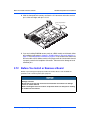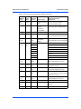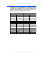
1
CPCI-6020 CompactPCI Single Board
Computer
Installation and Use
6806800A51C
February 2008
©
Copyright 2008, 2007 Motorola
All rights reserved.
Trademarks
Motorola® and the stylized M logo are trademarks registered in the U.S. Patent and Trademark Office.
PowerPC® is a registered trademark of International Business Machines and is used by Motorola Inc. under license from IBM
Corporation.
CompactPCI® is a registered trademark of PCI Industrial Computer Manufacturers Group. All other product or service names
mentioned in this document are trademarks or registered trademarks of their respective holders.
All other product or service names mentioned in this document are the property of their respective holders.
Notice
While reasonable efforts have been made to assure the accuracy of this document, Motorola assumes no liability resulting from any
omissions in this document, or from the use of the information obtained therein. Motorola reserves the right to revise this document
and to make changes from time to time in the content hereof without obligation of Motorola to notify any person of such revision or
changes.
Electronic versions of this material may be read online, downloaded for personal use, or referenced in another document as a URL to
a Motorola website. The text itself may not be published commercially in print or electronic form, edited, translated, or otherwise altered
without the permission of Motorola,
It is possible that this publication may contain reference to or information about Motorola products (machines and programs),
programming, or services that are not available in your country. Such references or information must not be construed to mean that
Motorola intends to announce such Motorola products, programming, or services in your country.
Limited and Restricted Rights Legend
If the documentation contained herein is supplied, directly or indirectly, to the U.S. Government, the following notice shall apply unless
otherwise agreed to in writing by Motorola.
Use, duplication, or disclosure by the Government is subject to restrictions as set forth in subparagraph (b)(3) of the Rights in Technical
Data clause at DFARS 252.227-7013 (Nov. 1995) and of the Rights in Noncommercial Computer Software and Documentation clause
at DFARS 252.227-7014 (Jun. 1995).
Contact Address
Motorola Inc.
ECC Embedded Communications Computing
2900 South Diablo Way, Suite 190
Tempe, Arizona 85282
Contents
About this Manual . . . . . . . . . . . . . . . . . . . . . . . . . . . . . . . . . . . . . . . . . . . . . . . . . . . . . . . . . . . . . . . . . . 13
Safety Notes. . . . . . . . . . . . . . . . . . . . . . . . . . . . . . . . . . . . . . . . . . . . . . . . . . . . . . . . . . . . . . . . . . . . . . . 19
Sicherheitshinweise . . . . . . . . . . . . . . . . . . . . . . . . . . . . . . . . . . . . . . . . . . . . . . . . . . . . . . . . . . . . . . . . 25
1
Introduction . . . . . . . . . . . . . . . . . . . . . . . . . . . . . . . . . . . . . . . . . . . . . . . . . . . . . . . . . . . . . . . . . . . . 31
1.1
1.2
1.3
2
Features . . . . . . . . . . . . . . . . . . . . . . . . . . . . . . . . . . . . . . . . . . . . . . . . . . . . . . . . . . . . . . . . . .
Standard Compliances . . . . . . . . . . . . . . . . . . . . . . . . . . . . . . . . . . . . . . . . . . . . . . . . . . . . . . .
Ordering Information . . . . . . . . . . . . . . . . . . . . . . . . . . . . . . . . . . . . . . . . . . . . . . . . . . . . . . . . .
1.3.1 Supported Board Models . . . . . . . . . . . . . . . . . . . . . . . . . . . . . . . . . . . . . . . . . . . . . . . .
1.3.2 Board Accessories . . . . . . . . . . . . . . . . . . . . . . . . . . . . . . . . . . . . . . . . . . . . . . . . . . . . .
31
32
33
33
34
Hardware Preparation and Installation . . . . . . . . . . . . . . . . . . . . . . . . . . . . . . . . . . . . . . . . . . . . . . 35
2.1
2.2
2.3
2.4
2.5
Overview . . . . . . . . . . . . . . . . . . . . . . . . . . . . . . . . . . . . . . . . . . . . . . . . . . . . . . . . . . . . . . . . . .
Unpacking and Inspecting the Board . . . . . . . . . . . . . . . . . . . . . . . . . . . . . . . . . . . . . . . . . . . .
Overview of Start-up Procedure . . . . . . . . . . . . . . . . . . . . . . . . . . . . . . . . . . . . . . . . . . . . . . . .
Equipment Required . . . . . . . . . . . . . . . . . . . . . . . . . . . . . . . . . . . . . . . . . . . . . . . . . . . . . . . . .
Environmental and Power Requirements . . . . . . . . . . . . . . . . . . . . . . . . . . . . . . . . . . . . . . . . .
2.5.1 Environmental Requirements . . . . . . . . . . . . . . . . . . . . . . . . . . . . . . . . . . . . . . . . . . . . .
2.5.2 Power Requirements . . . . . . . . . . . . . . . . . . . . . . . . . . . . . . . . . . . . . . . . . . . . . . . . . . .
2.5.3 Thermal Requirements. . . . . . . . . . . . . . . . . . . . . . . . . . . . . . . . . . . . . . . . . . . . . . . . . .
2.6 Hardware Configuration . . . . . . . . . . . . . . . . . . . . . . . . . . . . . . . . . . . . . . . . . . . . . . . . . . . . . .
2.7 CPCI-6020 Baseboard Preparation . . . . . . . . . . . . . . . . . . . . . . . . . . . . . . . . . . . . . . . . . . . . .
2.8 Jumper Settings . . . . . . . . . . . . . . . . . . . . . . . . . . . . . . . . . . . . . . . . . . . . . . . . . . . . . . . . . . . .
2.8.1 Flash Bank Selection . . . . . . . . . . . . . . . . . . . . . . . . . . . . . . . . . . . . . . . . . . . . . . . . . . .
2.8.2 Harrier Power Up Configuration Header . . . . . . . . . . . . . . . . . . . . . . . . . . . . . . . . . . . .
2.8.3 PMC 66 MHz Disable . . . . . . . . . . . . . . . . . . . . . . . . . . . . . . . . . . . . . . . . . . . . . . . . . . .
2.8.4 Enable/Disable +12 V and -12 V Use. . . . . . . . . . . . . . . . . . . . . . . . . . . . . . . . . . . . . . .
2.8.5 Enable/Disable Lockdown of One or More Flash Blocks for Bank A . . . . . . . . . . . . . . .
2.8.6 Enable Write-Protect for Entire Flash on Bank A . . . . . . . . . . . . . . . . . . . . . . . . . . . . . .
2.8.7 Remote Switch . . . . . . . . . . . . . . . . . . . . . . . . . . . . . . . . . . . . . . . . . . . . . . . . . . . . . . . .
2.9 Hardware Installation . . . . . . . . . . . . . . . . . . . . . . . . . . . . . . . . . . . . . . . . . . . . . . . . . . . . . . . .
2.10 PMC Module Installation . . . . . . . . . . . . . . . . . . . . . . . . . . . . . . . . . . . . . . . . . . . . . . . . . . . . . .
2.11 CompactFlash Memory Card Installation . . . . . . . . . . . . . . . . . . . . . . . . . . . . . . . . . . . . . . . . .
2.12 Before You Install or Remove a Board . . . . . . . . . . . . . . . . . . . . . . . . . . . . . . . . . . . . . . . . . . .
2.12.1 Watch for Bent Pins or Other Damage. . . . . . . . . . . . . . . . . . . . . . . . . . . . . . . . . . . . . .
2.12.2 Use Caution When Installing or Removing Boards . . . . . . . . . . . . . . . . . . . . . . . . . . . .
CPCI-6020 CompactPCI Single Board Computer Installation and Use (6806800A51C)
35
35
36
37
37
37
39
39
39
40
41
41
42
42
42
43
43
43
43
44
46
47
48
48
3
Contents
2.12.3 Understanding Hot Swap . . . . . . . . . . . . . . . . . . . . . . . . . . . . . . . . . . . . . . . . . . . . . . . .
2.12.4 Recognize Different Injector/Ejector Lever Types . . . . . . . . . . . . . . . . . . . . . . . . . . . . .
2.12.5 Verify Slot Usage . . . . . . . . . . . . . . . . . . . . . . . . . . . . . . . . . . . . . . . . . . . . . . . . . . . . . .
2.12.6 Preserve EMI Compliance . . . . . . . . . . . . . . . . . . . . . . . . . . . . . . . . . . . . . . . . . . . . . . .
2.13 Installing and Removing a Module . . . . . . . . . . . . . . . . . . . . . . . . . . . . . . . . . . . . . . . . . . . . . .
2.14 Startup and Operation . . . . . . . . . . . . . . . . . . . . . . . . . . . . . . . . . . . . . . . . . . . . . . . . . . . . . . . .
2.15 System Considerations . . . . . . . . . . . . . . . . . . . . . . . . . . . . . . . . . . . . . . . . . . . . . . . . . . . . . . .
3
Controls, LEDs, and Connectors. . . . . . . . . . . . . . . . . . . . . . . . . . . . . . . . . . . . . . . . . . . . . . . . . . . 57
3.1
3.2
3.3
3.4
4
Overview . . . . . . . . . . . . . . . . . . . . . . . . . . . . . . . . . . . . . . . . . . . . . . . . . . . . . . . . . . . . . . . . . .
CPCI-6020 Baseboard Layout . . . . . . . . . . . . . . . . . . . . . . . . . . . . . . . . . . . . . . . . . . . . . . . . .
Front Panel Connectors and LEDs . . . . . . . . . . . . . . . . . . . . . . . . . . . . . . . . . . . . . . . . . . . . . .
3.3.1 Front Panel Ethernet Port. . . . . . . . . . . . . . . . . . . . . . . . . . . . . . . . . . . . . . . . . . . . . . . .
3.3.2 Front Panel Asynchronous Serial Port . . . . . . . . . . . . . . . . . . . . . . . . . . . . . . . . . . . . .
3.3.3 Front Panel USB ports . . . . . . . . . . . . . . . . . . . . . . . . . . . . . . . . . . . . . . . . . . . . . . . . . .
3.3.4 ABORT# Switch . . . . . . . . . . . . . . . . . . . . . . . . . . . . . . . . . . . . . . . . . . . . . . . . . . . . . . .
3.3.5 RESET# Switch . . . . . . . . . . . . . . . . . . . . . . . . . . . . . . . . . . . . . . . . . . . . . . . . . . . . . . .
3.3.6 Front Panel LEDs . . . . . . . . . . . . . . . . . . . . . . . . . . . . . . . . . . . . . . . . . . . . . . . . . . . . . .
Connector Pin Assignments . . . . . . . . . . . . . . . . . . . . . . . . . . . . . . . . . . . . . . . . . . . . . . . . . . .
3.4.1 CompactPCI Bus Connectors . . . . . . . . . . . . . . . . . . . . . . . . . . . . . . . . . . . . . . . . . . . .
3.4.2 CompactPCI User I/O Connector . . . . . . . . . . . . . . . . . . . . . . . . . . . . . . . . . . . . . . . . . .
3.4.3 CompactPCI User I/O Connector . . . . . . . . . . . . . . . . . . . . . . . . . . . . . . . . . . . . . . . . . .
3.4.4 CompactPCI User I/O Connector . . . . . . . . . . . . . . . . . . . . . . . . . . . . . . . . . . . . . . . . .
3.4.5 Memory Mezzanine Connectors. . . . . . . . . . . . . . . . . . . . . . . . . . . . . . . . . . . . . . . . . . .
3.4.6 PCI Mezzanine Card (PMC) Connectors . . . . . . . . . . . . . . . . . . . . . . . . . . . . . . . . . . . .
3.4.7 Lock Down Flash Enable Jumper. . . . . . . . . . . . . . . . . . . . . . . . . . . . . . . . . . . . . . . . . .
3.4.8 PMC 66 Mhz Disable Jumper. . . . . . . . . . . . . . . . . . . . . . . . . . . . . . . . . . . . . . . . . . . . .
3.4.9 Remote Switch Connector . . . . . . . . . . . . . . . . . . . . . . . . . . . . . . . . . . . . . . . . . . . . . . .
3.4.10 Flash Write Protect Enable Jumper . . . . . . . . . . . . . . . . . . . . . . . . . . . . . . . . . . . . . . . .
3.4.11 Harrier Power Up Configuration . . . . . . . . . . . . . . . . . . . . . . . . . . . . . . . . . . . . . . . . . . .
3.4.12 Xport Flash Bank Select Header . . . . . . . . . . . . . . . . . . . . . . . . . . . . . . . . . . . . . . . . . .
3.4.13 RISCWatch Header . . . . . . . . . . . . . . . . . . . . . . . . . . . . . . . . . . . . . . . . . . . . . . . . . . . .
3.4.14 Mictor Debug Connector . . . . . . . . . . . . . . . . . . . . . . . . . . . . . . . . . . . . . . . . . . . . . . . .
57
57
58
58
59
59
60
60
60
60
60
63
64
65
67
68
72
73
73
73
74
74
74
75
Functional Description . . . . . . . . . . . . . . . . . . . . . . . . . . . . . . . . . . . . . . . . . . . . . . . . . . . . . . . . . . . 81
4.1
4.2
4.3
4
48
49
50
50
51
54
55
Overview . . . . . . . . . . . . . . . . . . . . . . . . . . . . . . . . . . . . . . . . . . . . . . . . . . . . . . . . . . . . . . . . . .
Block Diagram . . . . . . . . . . . . . . . . . . . . . . . . . . . . . . . . . . . . . . . . . . . . . . . . . . . . . . . . . . . . . .
Local PCI Bus Resources . . . . . . . . . . . . . . . . . . . . . . . . . . . . . . . . . . . . . . . . . . . . . . . . . . . . .
4.3.1 PCI Bus A Resources. . . . . . . . . . . . . . . . . . . . . . . . . . . . . . . . . . . . . . . . . . . . . . . . . . .
4.3.1.1 Local CompactPCI Bus . . . . . . . . . . . . . . . . . . . . . . . . . . . . . . . . . . . . . . . . .
4.3.1.2 Remote (Expansion) CompactPCI Bus . . . . . . . . . . . . . . . . . . . . . . . . . . . . .
4.3.1.3 Primary Ethernet Channel . . . . . . . . . . . . . . . . . . . . . . . . . . . . . . . . . . . . . . .
4.3.1.4 ISA Bridge, Including EIDE Function . . . . . . . . . . . . . . . . . . . . . . . . . . . . . . .
4.3.1.5 EIDE Interface . . . . . . . . . . . . . . . . . . . . . . . . . . . . . . . . . . . . . . . . . . . . . . . .
4.3.1.6 ISA Bus Resources . . . . . . . . . . . . . . . . . . . . . . . . . . . . . . . . . . . . . . . . . . . .
81
82
83
83
83
83
83
84
84
84
CPCI-6020 CompactPCI Single Board Computer Installation and Use (6806800A51C)
Contents
4.4
4.5
4.6
4.7
4.8
4.9
4.10
4.11
4.12
4.13
4.3.1.7 Synchronous Serial Ports . . . . . . . . . . . . . . . . . . . . . . . . . . . . . . . . . . . . . . . . 84
4.3.1.8 USB Controller . . . . . . . . . . . . . . . . . . . . . . . . . . . . . . . . . . . . . . . . . . . . . . . . 85
PCI Bus B Resources . . . . . . . . . . . . . . . . . . . . . . . . . . . . . . . . . . . . . . . . . . . . . . . . . . . . . . . . 85
4.4.1 PMC Slot . . . . . . . . . . . . . . . . . . . . . . . . . . . . . . . . . . . . . . . . . . . . . . . . . . . . . . . . . . . . 85
4.4.2 Secondary Ethernet Channel . . . . . . . . . . . . . . . . . . . . . . . . . . . . . . . . . . . . . . . . . . . . . 86
Processor Bus Resources . . . . . . . . . . . . . . . . . . . . . . . . . . . . . . . . . . . . . . . . . . . . . . . . . . . . 87
4.5.1 Processor . . . . . . . . . . . . . . . . . . . . . . . . . . . . . . . . . . . . . . . . . . . . . . . . . . . . . . . . . . . . 87
4.5.2 L2 Cache . . . . . . . . . . . . . . . . . . . . . . . . . . . . . . . . . . . . . . . . . . . . . . . . . . . . . . . . . . . . 87
Harrier System Memory Controller and PCI Host Bridge ASIC . . . . . . . . . . . . . . . . . . . . . . . . 87
4.6.1 Dual Harrier Assignments . . . . . . . . . . . . . . . . . . . . . . . . . . . . . . . . . . . . . . . . . . . . . . . 88
4.6.2 Harrier Power-Up Configuration . . . . . . . . . . . . . . . . . . . . . . . . . . . . . . . . . . . . . . . . . . . 88
4.6.3 Debug Connector . . . . . . . . . . . . . . . . . . . . . . . . . . . . . . . . . . . . . . . . . . . . . . . . . . . . . . 90
4.6.4 PPC Bus Arbitration . . . . . . . . . . . . . . . . . . . . . . . . . . . . . . . . . . . . . . . . . . . . . . . . . . . . 90
ECC Memory Bus Resources . . . . . . . . . . . . . . . . . . . . . . . . . . . . . . . . . . . . . . . . . . . . . . . . . . 90
4.7.1 Harrier A Memory Bus . . . . . . . . . . . . . . . . . . . . . . . . . . . . . . . . . . . . . . . . . . . . . . . . . . 90
4.7.2 Harrier B Memory Bus . . . . . . . . . . . . . . . . . . . . . . . . . . . . . . . . . . . . . . . . . . . . . . . . . . 91
4.7.3 RAM500 Memory Mezzanine . . . . . . . . . . . . . . . . . . . . . . . . . . . . . . . . . . . . . . . . . . . . . 91
Harrier Xport Resources . . . . . . . . . . . . . . . . . . . . . . . . . . . . . . . . . . . . . . . . . . . . . . . . . . . . . . 91
4.8.1 Harrier A, Channel 0 - Onboard Bank A Flash . . . . . . . . . . . . . . . . . . . . . . . . . . . . . . . . 92
4.8.2 Harrier A, Channel 1 - Socketed Bank B Flash . . . . . . . . . . . . . . . . . . . . . . . . . . . . . . . 92
4.8.3 Harrier A, Channel 2 - NVRAM, RTC, External Register Set . . . . . . . . . . . . . . . . . . . . . 92
4.8.4 Harrier A, Channel 3. . . . . . . . . . . . . . . . . . . . . . . . . . . . . . . . . . . . . . . . . . . . . . . . . . . . 92
4.8.5 Harrier B, Channel 0, 1, 2 and 3. . . . . . . . . . . . . . . . . . . . . . . . . . . . . . . . . . . . . . . . . . . 92
Other Harrier Resources . . . . . . . . . . . . . . . . . . . . . . . . . . . . . . . . . . . . . . . . . . . . . . . . . . . . . . 93
4.9.1 I2C Bus Resources - Serial EEPROM . . . . . . . . . . . . . . . . . . . . . . . . . . . . . . . . . . . . . . 93
4.9.2 Asynchronous Serial Ports . . . . . . . . . . . . . . . . . . . . . . . . . . . . . . . . . . . . . . . . . . . . . . . 93
4.9.3 32-Bit Timers . . . . . . . . . . . . . . . . . . . . . . . . . . . . . . . . . . . . . . . . . . . . . . . . . . . . . . . . . 93
4.9.4 Watchdog Timers . . . . . . . . . . . . . . . . . . . . . . . . . . . . . . . . . . . . . . . . . . . . . . . . . . . . . . 93
Other Board Resources . . . . . . . . . . . . . . . . . . . . . . . . . . . . . . . . . . . . . . . . . . . . . . . . . . . . . . 94
4.10.1 Miscellaneous Control and Status . . . . . . . . . . . . . . . . . . . . . . . . . . . . . . . . . . . . . . . . . 94
4.10.2 Clock Generator . . . . . . . . . . . . . . . . . . . . . . . . . . . . . . . . . . . . . . . . . . . . . . . . . . . . . . . 94
4.10.3 Onboard Power Supplies . . . . . . . . . . . . . . . . . . . . . . . . . . . . . . . . . . . . . . . . . . . . . . . . 95
4.10.4 Board Reset Logic . . . . . . . . . . . . . . . . . . . . . . . . . . . . . . . . . . . . . . . . . . . . . . . . . . . . . 95
4.10.5 Soft Reset . . . . . . . . . . . . . . . . . . . . . . . . . . . . . . . . . . . . . . . . . . . . . . . . . . . . . . . . . . . 97
4.10.6 Front Panel Resources. . . . . . . . . . . . . . . . . . . . . . . . . . . . . . . . . . . . . . . . . . . . . . . . . . 97
4.10.7 ABORT# and RESET# Switches . . . . . . . . . . . . . . . . . . . . . . . . . . . . . . . . . . . . . . . . . . 97
4.10.8 On-Board LEDs . . . . . . . . . . . . . . . . . . . . . . . . . . . . . . . . . . . . . . . . . . . . . . . . . . . . . . . 98
4.10.9 Harrier Power Up Configuration Header . . . . . . . . . . . . . . . . . . . . . . . . . . . . . . . . . . . . 98
Hot Swap Support . . . . . . . . . . . . . . . . . . . . . . . . . . . . . . . . . . . . . . . . . . . . . . . . . . . . . . . . . . . 98
High Availability Support . . . . . . . . . . . . . . . . . . . . . . . . . . . . . . . . . . . . . . . . . . . . . . . . . . . . . . 98
4.12.1 HSC Bridge Board Interface. . . . . . . . . . . . . . . . . . . . . . . . . . . . . . . . . . . . . . . . . . . . . . 98
4.12.2 Local CompactPCI Bus Interface . . . . . . . . . . . . . . . . . . . . . . . . . . . . . . . . . . . . . . . . . . 99
4.12.3 Secondary Bus Arbitration . . . . . . . . . . . . . . . . . . . . . . . . . . . . . . . . . . . . . . . . . . . . . . . 99
4.12.4 Secondary Bus Tri-Stating . . . . . . . . . . . . . . . . . . . . . . . . . . . . . . . . . . . . . . . . . . . . . . . 99
4.12.5 System Slot Hot Swap . . . . . . . . . . . . . . . . . . . . . . . . . . . . . . . . . . . . . . . . . . . . . . . . . . 99
EIDE Interface . . . . . . . . . . . . . . . . . . . . . . . . . . . . . . . . . . . . . . . . . . . . . . . . . . . . . . . . . . . . . 100
CPCI-6020 CompactPCI Single Board Computer Installation and Use (6806800A51C)
5
Contents
4.14
4.15
4.16
4.17
4.18
4.19
4.20
4.21
4.22
4.23
4.24
4.25
4.26
4.27
5
6.5
6.6
107
107
108
108
108
110
110
114
Overview . . . . . . . . . . . . . . . . . . . . . . . . . . . . . . . . . . . . . . . . . . . . . . . . . . . . . . . . . . . . . . . . .
RAM500 Description . . . . . . . . . . . . . . . . . . . . . . . . . . . . . . . . . . . . . . . . . . . . . . . . . . . . . . . .
RAM500 Module Installation . . . . . . . . . . . . . . . . . . . . . . . . . . . . . . . . . . . . . . . . . . . . . . . . . .
Features . . . . . . . . . . . . . . . . . . . . . . . . . . . . . . . . . . . . . . . . . . . . . . . . . . . . . . . . . . . . . . . . .
6.4.1 SROM. . . . . . . . . . . . . . . . . . . . . . . . . . . . . . . . . . . . . . . . . . . . . . . . . . . . . . . . . . . . . .
6.4.2 Host Clock Logic . . . . . . . . . . . . . . . . . . . . . . . . . . . . . . . . . . . . . . . . . . . . . . . . . . . . .
6.4.3 Serial Presence Detect (SPD) Data . . . . . . . . . . . . . . . . . . . . . . . . . . . . . . . . . . . . . . .
RAM500 Connectors . . . . . . . . . . . . . . . . . . . . . . . . . . . . . . . . . . . . . . . . . . . . . . . . . . . . . . . .
6.5.1 Bottom Side Memory Expansion Connector (P1). . . . . . . . . . . . . . . . . . . . . . . . . . . . .
6.5.2 Top Side Memory Expansion Connector (J1) . . . . . . . . . . . . . . . . . . . . . . . . . . . . . . .
RAM500 Programming Issues . . . . . . . . . . . . . . . . . . . . . . . . . . . . . . . . . . . . . . . . . . . . . . . .
117
117
118
119
119
120
120
120
120
123
125
Transition Module Preparation and Installation. . . . . . . . . . . . . . . . . . . . . . . . . . . . . . . . . . . . . . 127
7.1
7.2
7.3
6
PPCBug Overview . . . . . . . . . . . . . . . . . . . . . . . . . . . . . . . . . . . . . . . . . . . . . . . . . . . . . . . . .
PPCBug Basics . . . . . . . . . . . . . . . . . . . . . . . . . . . . . . . . . . . . . . . . . . . . . . . . . . . . . . . . . . . .
Memory Requirements . . . . . . . . . . . . . . . . . . . . . . . . . . . . . . . . . . . . . . . . . . . . . . . . . . . . . .
PPCBug Implementation . . . . . . . . . . . . . . . . . . . . . . . . . . . . . . . . . . . . . . . . . . . . . . . . . . . . .
MPU, Hardware and Firmware Initialization . . . . . . . . . . . . . . . . . . . . . . . . . . . . . . . . . . . . . .
Using PPCBug . . . . . . . . . . . . . . . . . . . . . . . . . . . . . . . . . . . . . . . . . . . . . . . . . . . . . . . . . . . .
Debugger Commands . . . . . . . . . . . . . . . . . . . . . . . . . . . . . . . . . . . . . . . . . . . . . . . . . . . . . . .
Diagnostic Tests . . . . . . . . . . . . . . . . . . . . . . . . . . . . . . . . . . . . . . . . . . . . . . . . . . . . . . . . . . .
RAM500 Memory Expansion Module . . . . . . . . . . . . . . . . . . . . . . . . . . . . . . . . . . . . . . . . . . . . . . 117
6.1
6.2
6.3
6.4
7
100
100
100
101
101
101
103
103
104
105
105
105
105
105
Firmware . . . . . . . . . . . . . . . . . . . . . . . . . . . . . . . . . . . . . . . . . . . . . . . . . . . . . . . . . . . . . . . . . . . . . 107
5.1
5.2
5.3
5.4
5.5
5.6
5.7
5.8
6
Ethernet Interface . . . . . . . . . . . . . . . . . . . . . . . . . . . . . . . . . . . . . . . . . . . . . . . . . . . . . . . . . .
Hot Swap Support . . . . . . . . . . . . . . . . . . . . . . . . . . . . . . . . . . . . . . . . . . . . . . . . . . . . . . . . . .
PMC Interface Module (PIM) . . . . . . . . . . . . . . . . . . . . . . . . . . . . . . . . . . . . . . . . . . . . . . . . .
Asynchronous Serial Ports . . . . . . . . . . . . . . . . . . . . . . . . . . . . . . . . . . . . . . . . . . . . . . . . . . .
Synchronous Serial Ports . . . . . . . . . . . . . . . . . . . . . . . . . . . . . . . . . . . . . . . . . . . . . . . . . . . .
I/O Signal Multiplexing (IOMUX) . . . . . . . . . . . . . . . . . . . . . . . . . . . . . . . . . . . . . . . . . . . . . . .
Serial Interface Modules (SIM) . . . . . . . . . . . . . . . . . . . . . . . . . . . . . . . . . . . . . . . . . . . . . . . .
PMC Interface Module (PIM) . . . . . . . . . . . . . . . . . . . . . . . . . . . . . . . . . . . . . . . . . . . . . . . . .
PMC Interface Module Form Factor . . . . . . . . . . . . . . . . . . . . . . . . . . . . . . . . . . . . . . . . . . . .
PMC Interface Connector . . . . . . . . . . . . . . . . . . . . . . . . . . . . . . . . . . . . . . . . . . . . . . . . . . . .
Host I/O Connector . . . . . . . . . . . . . . . . . . . . . . . . . . . . . . . . . . . . . . . . . . . . . . . . . . . . . . . . .
Speaker Port . . . . . . . . . . . . . . . . . . . . . . . . . . . . . . . . . . . . . . . . . . . . . . . . . . . . . . . . . . . . . .
Floppy Disk Port . . . . . . . . . . . . . . . . . . . . . . . . . . . . . . . . . . . . . . . . . . . . . . . . . . . . . . . . . . .
Mouse and Keyboard Port . . . . . . . . . . . . . . . . . . . . . . . . . . . . . . . . . . . . . . . . . . . . . . . . . . .
Overview . . . . . . . . . . . . . . . . . . . . . . . . . . . . . . . . . . . . . . . . . . . . . . . . . . . . . . . . . . . . . . . . .
General Description . . . . . . . . . . . . . . . . . . . . . . . . . . . . . . . . . . . . . . . . . . . . . . . . . . . . . . . .
7.2.1 Component Layout . . . . . . . . . . . . . . . . . . . . . . . . . . . . . . . . . . . . . . . . . . . . . . . . . . . .
7.2.2 Rear Panel Connectors . . . . . . . . . . . . . . . . . . . . . . . . . . . . . . . . . . . . . . . . . . . . . . . .
Unpacking and Inspecting the RTM . . . . . . . . . . . . . . . . . . . . . . . . . . . . . . . . . . . . . . . . . . . .
127
127
129
130
131
CPCI-6020 CompactPCI Single Board Computer Installation and Use (6806800A51C)
Contents
7.4
7.5
7.6
7.7
7.8
7.9
8
131
131
132
133
135
136
138
140
141
143
143
143
146
146
147
147
148
148
149
149
150
CNFG and ENV Commands . . . . . . . . . . . . . . . . . . . . . . . . . . . . . . . . . . . . . . . . . . . . . . . . . . . . . . 151
8.1
8.2
8.3
8.4
A
Preparing the Transition Module . . . . . . . . . . . . . . . . . . . . . . . . . . . . . . . . . . . . . . . . . . . . . . .
7.4.1 Serial Ports 1 and 2 . . . . . . . . . . . . . . . . . . . . . . . . . . . . . . . . . . . . . . . . . . . . . . . . . . .
7.4.2 Serial Ports 3 and 4 . . . . . . . . . . . . . . . . . . . . . . . . . . . . . . . . . . . . . . . . . . . . . . . . . . .
7.4.3 Serial Interface Module Circuitry . . . . . . . . . . . . . . . . . . . . . . . . . . . . . . . . . . . . . . . . .
7.4.4 Port Configuration . . . . . . . . . . . . . . . . . . . . . . . . . . . . . . . . . . . . . . . . . . . . . . . . . . . .
Installing the SIMs . . . . . . . . . . . . . . . . . . . . . . . . . . . . . . . . . . . . . . . . . . . . . . . . . . . . . . . . . .
Installing the PIM . . . . . . . . . . . . . . . . . . . . . . . . . . . . . . . . . . . . . . . . . . . . . . . . . . . . . . . . . .
Installing and Removing the Transition Module . . . . . . . . . . . . . . . . . . . . . . . . . . . . . . . . . . .
Connectors and Cables . . . . . . . . . . . . . . . . . . . . . . . . . . . . . . . . . . . . . . . . . . . . . . . . . . . . .
Connector Pin Assignments . . . . . . . . . . . . . . . . . . . . . . . . . . . . . . . . . . . . . . . . . . . . . . . . . .
7.9.1 CompactPCI Connectors . . . . . . . . . . . . . . . . . . . . . . . . . . . . . . . . . . . . . . . . . . . . . . .
7.9.2 PMC I/O Module Connector . . . . . . . . . . . . . . . . . . . . . . . . . . . . . . . . . . . . . . . . . . . . .
7.9.3 10BaseT/100BaseTx Connectors . . . . . . . . . . . . . . . . . . . . . . . . . . . . . . . . . . . . . . . .
7.9.4 COM1 Connector . . . . . . . . . . . . . . . . . . . . . . . . . . . . . . . . . . . . . . . . . . . . . . . . . . . . .
7.9.5 COM2 Header . . . . . . . . . . . . . . . . . . . . . . . . . . . . . . . . . . . . . . . . . . . . . . . . . . . . . . .
7.9.6 EIDE Header . . . . . . . . . . . . . . . . . . . . . . . . . . . . . . . . . . . . . . . . . . . . . . . . . . . . . . . .
7.9.7 Floppy Port Header . . . . . . . . . . . . . . . . . . . . . . . . . . . . . . . . . . . . . . . . . . . . . . . . . . .
7.9.8 +5VDC Power Connector . . . . . . . . . . . . . . . . . . . . . . . . . . . . . . . . . . . . . . . . . . . . . . .
7.9.9 Keyboard/Mouse Connector. . . . . . . . . . . . . . . . . . . . . . . . . . . . . . . . . . . . . . . . . . . . .
7.9.10 Sync/Async Serial Ports . . . . . . . . . . . . . . . . . . . . . . . . . . . . . . . . . . . . . . . . . . . . . . . .
7.9.11 Speaker Output Header . . . . . . . . . . . . . . . . . . . . . . . . . . . . . . . . . . . . . . . . . . . . . . . .
Overview . . . . . . . . . . . . . . . . . . . . . . . . . . . . . . . . . . . . . . . . . . . . . . . . . . . . . . . . . . . . . . . . .
CNFG - Configure Board Information . . . . . . . . . . . . . . . . . . . . . . . . . . . . . . . . . . . . . . . . . . .
ENV - Set Environment . . . . . . . . . . . . . . . . . . . . . . . . . . . . . . . . . . . . . . . . . . . . . . . . . . . . . .
Configuring the PPCBug Parameters . . . . . . . . . . . . . . . . . . . . . . . . . . . . . . . . . . . . . . . . . . .
151
151
152
152
Related Documentation . . . . . . . . . . . . . . . . . . . . . . . . . . . . . . . . . . . . . . . . . . . . . . . . . . . . . . . . . 161
A.1
A.2
A.3
Embedded Communications Computing Documents . . . . . . . . . . . . . . . . . . . . . . . . . . . . . . . 161
Manufacturers’ Documents . . . . . . . . . . . . . . . . . . . . . . . . . . . . . . . . . . . . . . . . . . . . . . . . . . . 161
Related Specifications . . . . . . . . . . . . . . . . . . . . . . . . . . . . . . . . . . . . . . . . . . . . . . . . . . . . . . 162
Index . . . . . . . . . . . . . . . . . . . . . . . . . . . . . . . . . . . . . . . . . . . . . . . . . . . . . . . . . . . . . . . . . . . . . . . . . . . . 165
CPCI-6020 CompactPCI Single Board Computer Installation and Use (6806800A51C)
7
Contents
8
CPCI-6020 CompactPCI Single Board Computer Installation and Use (6806800A51C)
List of Tables
Table 1-1
Table 1-2
Table 2-1
Table 2-2
Table 2-3
Table 2-4
Table 3-1
Table 3-2
Table 3-3
Table 3-4
Table 3-5
Table 3-6
Table 3-7
Table 3-8
Table 3-9
Table 3-10
Table 3-11
Table 3-12
Table 3-13
Table 3-14
Table 3-15
Table 3-16
Table 3-17
Table 3-18
Table 3-19
Table 3-20
Table 3-21
Table 3-22
Table 3-23
Table 3-24
Table 3-25
Table 4-1
Table 4-2
Table 4-3
Table 4-4
Table 4-5
Table 4-6
Table 4-7
Table 5-1
Table 5-2
Features . . . . . . . . . . . . . . . . . . . . . . . . . . . . . . . . . . . . . . . . . . . . . . . . . . . . . . . . . . . . 31
Board Standard Compliances . . . . . . . . . . . . . . . . . . . . . . . . . . . . . . . . . . . . . . . . . . . 32
Startup Overview . . . . . . . . . . . . . . . . . . . . . . . . . . . . . . . . . . . . . . . . . . . . . . . . . . . . . 36
Specifications . . . . . . . . . . . . . . . . . . . . . . . . . . . . . . . . . . . . . . . . . . . . . . . . . . . . . . . . 38
Baseboard and RTM Power Requirements . . . . . . . . . . . . . . . . . . . . . . . . . . . . . . . . . 39
Slot Usage Indicators . . . . . . . . . . . . . . . . . . . . . . . . . . . . . . . . . . . . . . . . . . . . . . . . . . 50
Ethernet Connector Pin Assignments . . . . . . . . . . . . . . . . . . . . . . . . . . . . . . . . . . . . . 58
COM1 Pin Assignments . . . . . . . . . . . . . . . . . . . . . . . . . . . . . . . . . . . . . . . . . . . . . . . . 59
USB Port 1 . . . . . . . . . . . . . . . . . . . . . . . . . . . . . . . . . . . . . . . . . . . . . . . . . . . . . . . . . . 59
USB Port 0 . . . . . . . . . . . . . . . . . . . . . . . . . . . . . . . . . . . . . . . . . . . . . . . . . . . . . . . . . . 59
Front Panel LEDs . . . . . . . . . . . . . . . . . . . . . . . . . . . . . . . . . . . . . . . . . . . . . . . . . . . . . 60
J1 CompactPCI Connector . . . . . . . . . . . . . . . . . . . . . . . . . . . . . . . . . . . . . . . . . . . . . 61
J2 CompactPCI Connector . . . . . . . . . . . . . . . . . . . . . . . . . . . . . . . . . . . . . . . . . . . . . 61
J3 CompactPCI User I/O Connector . . . . . . . . . . . . . . . . . . . . . . . . . . . . . . . . . . . . . . 63
Signal Descriptions for the J3 Connector . . . . . . . . . . . . . . . . . . . . . . . . . . . . . . . . . . . 63
J4 Local PCI Expansion Connector Pinout . . . . . . . . . . . . . . . . . . . . . . . . . . . . . . . . . 64
J5 User I/O Connector . . . . . . . . . . . . . . . . . . . . . . . . . . . . . . . . . . . . . . . . . . . . . . . . . 65
J5 Signal Descriptions . . . . . . . . . . . . . . . . . . . . . . . . . . . . . . . . . . . . . . . . . . . . . . . . . 65
J8 and J27 Memory Mezzanine Connector . . . . . . . . . . . . . . . . . . . . . . . . . . . . . . . . . 67
PMC Connector J11 Pin Assignments . . . . . . . . . . . . . . . . . . . . . . . . . . . . . . . . . . . . . 68
J12 PMC Connector J12 Pin Assignments . . . . . . . . . . . . . . . . . . . . . . . . . . . . . . . . . 69
PMC Connector J13 Pin Assignments . . . . . . . . . . . . . . . . . . . . . . . . . . . . . . . . . . . . . 70
PMC Connector J14 Pin Assignments . . . . . . . . . . . . . . . . . . . . . . . . . . . . . . . . . . . . . 71
J17 Lock Down Flash Enable Jumper . . . . . . . . . . . . . . . . . . . . . . . . . . . . . . . . . . . . . 72
J21 PMC 66 MHz Disable Jumper . . . . . . . . . . . . . . . . . . . . . . . . . . . . . . . . . . . . . . . . 73
J19 Remote Switch Connector . . . . . . . . . . . . . . . . . . . . . . . . . . . . . . . . . . . . . . . . . . 73
J20 Flash Write Protect Enable Jumper . . . . . . . . . . . . . . . . . . . . . . . . . . . . . . . . . . . . 73
J22 Harrier Power Up Configuration Header Pin Assignments . . . . . . . . . . . . . . . . . . 74
J24 Xport Flash Bank Select Header . . . . . . . . . . . . . . . . . . . . . . . . . . . . . . . . . . . . . . 74
J25 RISCWatch Header Pin Assignments . . . . . . . . . . . . . . . . . . . . . . . . . . . . . . . . . . 74
J28 Debug Connector . . . . . . . . . . . . . . . . . . . . . . . . . . . . . . . . . . . . . . . . . . . . . . . . . 75
Special Function Processor PMC Pins . . . . . . . . . . . . . . . . . . . . . . . . . . . . . . . . . . . . 86
Harrier Power-Up Configuration Settings . . . . . . . . . . . . . . . . . . . . . . . . . . . . . . . . . . . 88
Expansion SDRAM Memory Mezzanine Size Options . . . . . . . . . . . . . . . . . . . . . . . . . 91
Bank A Flash Options . . . . . . . . . . . . . . . . . . . . . . . . . . . . . . . . . . . . . . . . . . . . . . . . . 92
PPC to PCI Clock Ratios . . . . . . . . . . . . . . . . . . . . . . . . . . . . . . . . . . . . . . . . . . . . . . . 94
Reset Sources and Devices Affected . . . . . . . . . . . . . . . . . . . . . . . . . . . . . . . . . . . . . . 96
Multiplexing Sequence of the IOMX Function . . . . . . . . . . . . . . . . . . . . . . . . . . . . . . 102
Debugger Commands . . . . . . . . . . . . . . . . . . . . . . . . . . . . . . . . . . . . . . . . . . . . . . . . 111
Diagnostic Test Groups . . . . . . . . . . . . . . . . . . . . . . . . . . . . . . . . . . . . . . . . . . . . . . . 115
CPCI-6020 CompactPCI Single Board Computer Installation and Use (6806800A51C)
9
List of Tables
Table 6-1
Table 6-2
Table 6-3
Table 6-4
Table 7-1
Table 7-2
Table 7-3
Table 7-4
Table 7-5
Table 7-6
Table 7-7
Table 7-8
Table 7-9
Table 7-10
Table 7-11
Table 7-12
Table 7-13
Table 7-14
Table A-1
Table A-2
Table A-3
10
RAM500 SDRAM Memory Size Options . . . . . . . . . . . . . . . . . . . . . . . . . . . . . . . . . .
RAM500 Feature Summary . . . . . . . . . . . . . . . . . . . . . . . . . . . . . . . . . . . . . . . . . . . .
RAM500 Bottom Side Connector (P1) Pin Assignments . . . . . . . . . . . . . . . . . . . . . .
RAM500 Top Side Connector (J1) Pin Assignments . . . . . . . . . . . . . . . . . . . . . . . . .
SIM Model Numbers . . . . . . . . . . . . . . . . . . . . . . . . . . . . . . . . . . . . . . . . . . . . . . . . .
Rear Transition Module Connectors/Headers . . . . . . . . . . . . . . . . . . . . . . . . . . . . . .
Rear Transition Module Cables . . . . . . . . . . . . . . . . . . . . . . . . . . . . . . . . . . . . . . . . .
PMC I/O Module - Host I/O Connector Pin Assignments . . . . . . . . . . . . . . . . . . . . . .
PMC I/O Module - PMC I/O Connector Pin Assignments . . . . . . . . . . . . . . . . . . . . .
10BaseT/100BaseTx Connector Pin Assignments . . . . . . . . . . . . . . . . . . . . . . . . . .
COM1 Connector Pin Assignments . . . . . . . . . . . . . . . . . . . . . . . . . . . . . . . . . . . . . .
COM2 Header Pin Assignments . . . . . . . . . . . . . . . . . . . . . . . . . . . . . . . . . . . . . . . .
EIDE Header Pin Assignments . . . . . . . . . . . . . . . . . . . . . . . . . . . . . . . . . . . . . . . . .
Floppy Header Pin Assignments . . . . . . . . . . . . . . . . . . . . . . . . . . . . . . . . . . . . . . . .
+5Vdc Power Connector . . . . . . . . . . . . . . . . . . . . . . . . . . . . . . . . . . . . . . . . . . . . . .
Keyboard/Mouse Connector Pin Assignments . . . . . . . . . . . . . . . . . . . . . . . . . . . . . .
Sync/Async Serial Connector Pin Assignments . . . . . . . . . . . . . . . . . . . . . . . . . . . . .
Speaker Output Connector Pin Assignments . . . . . . . . . . . . . . . . . . . . . . . . . . . . . . .
Embedded Communications Computing Documents . . . . . . . . . . . . . . . . . . . . . . . . .
Manufacturers’ Documents . . . . . . . . . . . . . . . . . . . . . . . . . . . . . . . . . . . . . . . . . . . .
Related Specifications . . . . . . . . . . . . . . . . . . . . . . . . . . . . . . . . . . . . . . . . . . . . . . . .
118
119
120
123
132
141
142
143
144
146
146
147
147
148
148
149
149
150
161
161
162
CPCI-6020 CompactPCI Single Board Computer Installation and Use (6806800A51C)
List of Figures
Figure 2-1
Figure 2-2
Figure 2-3
Figure 3-1
Figure 3-2
Figure 4-1
Figure 4-2
Figure 4-3
Figure 4-4
Figure 4-5
Figure 7-1
Figure 7-2
Figure 7-3
Figure 7-4
Figure 7-5
Figure 7-6
Header Locations and Jumper Settings . . . . . . . . . . . . . . . . . . . . . . . . . . . . . . . . . . . . 41
Injector/Ejector Lever Types . . . . . . . . . . . . . . . . . . . . . . . . . . . . . . . . . . . . . . . . . . . . . 49
Start Up Flow Diagram . . . . . . . . . . . . . . . . . . . . . . . . . . . . . . . . . . . . . . . . . . . . . . . . . 55
Headers, Connectors and LEDs . . . . . . . . . . . . . . . . . . . . . . . . . . . . . . . . . . . . . . . . . . 57
Front Panel Connectors and LEDs . . . . . . . . . . . . . . . . . . . . . . . . . . . . . . . . . . . . . . . . 58
Block Diagram . . . . . . . . . . . . . . . . . . . . . . . . . . . . . . . . . . . . . . . . . . . . . . . . . . . . . . . 82
Reset Block Diagram . . . . . . . . . . . . . . . . . . . . . . . . . . . . . . . . . . . . . . . . . . . . . . . . . . 96
Serial Port Signal Multiplexing . . . . . . . . . . . . . . . . . . . . . . . . . . . . . . . . . . . . . . . . . . 101
P2MX Signal Timings . . . . . . . . . . . . . . . . . . . . . . . . . . . . . . . . . . . . . . . . . . . . . . . . . 103
PMC Interface Module Layout . . . . . . . . . . . . . . . . . . . . . . . . . . . . . . . . . . . . . . . . . . 104
Block Diagram . . . . . . . . . . . . . . . . . . . . . . . . . . . . . . . . . . . . . . . . . . . . . . . . . . . . . . 128
Component Layout . . . . . . . . . . . . . . . . . . . . . . . . . . . . . . . . . . . . . . . . . . . . . . . . . . . 129
Rear Panel Connectors, Cut-outs . . . . . . . . . . . . . . . . . . . . . . . . . . . . . . . . . . . . . . . 130
Ports 3 and 4 Header Settings . . . . . . . . . . . . . . . . . . . . . . . . . . . . . . . . . . . . . . . . . . 133
EIA-232-D DCE Ports 3 and 4 Configuration . . . . . . . . . . . . . . . . . . . . . . . . . . . . . . . 135
EIA-232-D DTE Ports 3 and 4 Configuration . . . . . . . . . . . . . . . . . . . . . . . . . . . . . . . 136
CPCI-6020 CompactPCI Single Board Computer Installation and Use (6806800A51C)
11
List of Figures
12
CPCI-6020 CompactPCI Single Board Computer Installation and Use (6806800A51C)
About this Manual
Overview of Contents
This manual provides the information required to install and configure an CPCI-6020 Single
Board Computer. Moreover, this manual provides specific preparation and installation
information and data applicable to the board. The CPCI-6020 was previously offered as the
MCP820 Single Board Computer.
The CPCI-6020 is a high-performance CompactPCI single board computer featuring the
MPC7410 with Alti-Vec™ technology for algorithmic intensive computational capabilities.
This manual is divided into the following chapters and appendices:
Safety Notes, a collection of standard product safety notes for the CPCI-6020 in English.
Sicherheitshinweise, a collection of standard product safety ntoes for the CPCI-6020 translated
to German.
Chapter 1, Introduction, lists the features of the CPCI-6020 baseboard, standards compliances,
model numbers for boards, memory, and RTMs.
Chapter 2, Hardware Preparation and Installation, includes a description of the CPCI-6020,
unpacking instructions, environmental and power requirement, and how to prepare and install
the CompactFlash, a PMC module, and the CPCI-6020 baseboard.
Chapter 3, Controls, LEDs, and Connectors provides illustrations of the board components and
face plate details. This chapter also gives descriptions for the onboard and front panel LEDs
and connections and pinout information for connectors, headers and jumpers.
Chapter 4, Functional Description describes the major features of the CPCI-6020 baseboard
and the CPCI-6020-MCPTM-01 transition module. These descriptions include both
programming and hardware characteristics of major components.
Chapter 5, Firmware describes the role, process and commands employed by the CPCI-6020
diagnostic and initialization firmware PPCBug. This chapter also briefly describes how to use
the debugger commands.
Chapter 6, RAM500 Memory Expansion Module provides information for installing the RAM500
memory mezzanine. If also provides information on pinouts and features.
Chapter 7, Transition Module Preparation and Installation, includes a description of the CPCI6020-MCPTM-01 rear transition module. The chapter provides illustrations of the RTM
components and face plate details. It describes jumper settings, port configuration diagrams,
and procedures for installing SIMs and PIMs. Pin assignment tables for the RTM are included
in this chapter.
Chapter 8, CNFG and ENV Commands describes how to use the CNFG and ENV commands
of PPCBug to modify certain parameters within the CPCI-6020.
CPCI-6020 CompactPCI Single Board Computer Installation and Use (6806800A51C)
13
About this Manual
Appendix A, Related Documentation provides listings for Motorola publications, manufacturer’s
documents and related industry specification for this product.
Abbreviations
This document uses the following abbreviations:
14
Abbreviation
Description
ACE
Asynchronous Communications Element
ANSI
American National Standards Institute
ASIC
Application Specific Integrated Circuit
BBRAM
Battery Backed-up RAM
BDFL
Board Fail
CF
Compact Flash
CHRP
Common Hardware Reference Platform
CMOS
Complementary metal oxide semiconductor
DCE
Data Circuit Termination
DTE
Data Terminal Equipment
EIDE
Enhanced Integrated Design Electronics
EMI
Electro Magnetic Interference
ESD
Electro Static Discharge
FDD
Floppy Disk Drive
GB
Gigabyte
HA
High Availability
HDD
Hard Disk Drive
HSC
Hot Swap Controller
IOMUX
I/O Signal Multiplexing
ISA
Industry Standard Architecture
KB
Kilobyte
MAC
Media Access Controller
MPU
Microprocessing Unit
Mbps
Megabits per second
MB
Megabyte
NVRAM
Non Volatile Random Access Memory
OHCI
Open Host Controller Interface
PF
Port Format
PHB
PCI Host Bridge
PHY
Physical Layer
PIB
PCI Arbiter
CPCI-6020 CompactPCI Single Board Computer Installation and Use (6806800A51C)
About this Manual
Abbreviation
Description
PIM
PMC Interface Module
PIO
Parallel Input Output
PIRQx
PCI Interrupts
PMC
Peripheral Mezzanine Card
PRP
PowerPC Reference Platform
PrPMC
Processor PMC
RISC
Reduced Instruction Set Computer
RoHS
Restriction of Hazardous Substances
SIM
Serial Interface Module
SMC
System Memory Controller
SPD
Serial Presence Detect
TA
Terminal Attach
UART
Universal Asynchronous Receiver-Transmitter
USB
Universal Serial Bus
VPD
Vital Product Data
Conventions
The following table describes the conventions used throughout this manual.
Notation
Description
0x00000000
Typical notation for hexadecimal numbers (digits
are 0 through F), for example used for addresses
and offsets
0b0000
Same for binary numbers (digits are 0 and 1)
bold
Used to emphasize a word
Screen
Used for on-screen output and code related
elements or commands in body text
Courier + Bold
Used to characterize user input and to separate it
from system output
Reference
Used for references and for table and figure
descriptions
File > Exit
Notation for selecting a submenu
<text>
Notation for variables and keys
[text]
Notation for software buttons to click on the
screen and parameter description
...
Repeated item for example node 1, node 2, ...,
node 12
CPCI-6020 CompactPCI Single Board Computer Installation and Use (6806800A51C)
15
About this Manual
Notation
Description
.
Omission of information from example/command
that is not necessary at the time being
.
.
..
Ranges, for example: 0..4 means one of the
integers 0,1,2,3, and 4 (used in registers)
|
Logical OR
Indicates a hazardous situation which, if not
avoided, could result in death or serious injury
Indicates a hazardous situation which, if not
avoided, may result in minor or moderate injury
Indicates a property damage message
No danger encountered. Pay attention to
important information
Summary of Changes
This manual has been revised and replaces all prior editions.
Part Number
Publication Date
6806800A36A
Description
First release. Replaces MCP820 SBC.
6806800A36B
January 2007
J24 Xport flash bank select header
description corrected.
6806800A36C
January 2008
Remove Winbond PC97317 for 6/6 version.
Legacy functionality remains via serial,
Ethernet, and CompactFlash components.
RoHS 6/6 compliancy.
Editorial and style changes to manual.
16
CPCI-6020 CompactPCI Single Board Computer Installation and Use (6806800A51C)
About this Manual
Comments and Suggestions
We welcome and appreciate your comments on our documentation. We want to know what you
think about our manuals and how we can make them better.
Mail comments to:
z
Motorola, Inc.
Embedded Communications Computing
2900 South Diablo Way, Suite 190
Tempe, Arizona 85282
z
[email protected]
In all your correspondence, please list your name, position, and company. Be sure to include
the title, part number, and revision of the manual and tell how you used it.
CPCI-6020 CompactPCI Single Board Computer Installation and Use (6806800A51C)
17
About this Manual
18
CPCI-6020 CompactPCI Single Board Computer Installation and Use (6806800A51C)
Safety Notes
This section provides warnings that precede potentially dangerous procedures
throughout this manual. Instructions contained in the warnings must be followed during
all phases of operation, service, and repair of this equipment. You should also employ
all other safety precautions necessary for the operation of the equipment in your
operating environment. Failure to comply with these precautions or with specific
warnings elsewhere in this manual could result in personal injury or damage to the
equipment.
Motorola intends to provide all necessary information to install and handle the product
in this manual. Because of the complexity of this product and its various uses, we do not
guarantee that the given information is complete. If you need additional information, ask
your Motorola representative.
The product has been designed to meet the standard industrial safety requirements. It
must not be used except in its specific area of office telecommunication industry and
industrial control.
Only personnel trained by Motorola or persons qualified in electronics or electrical
engineering are authorized to install, remove or maintain the product.
The information given in this manual is meant to complete the knowledge of a specialist
and must not be used as replacement for qualified personnel.
Keep away from live circuits inside the equipment. Operating personnel must not
remove equipment covers. Only Factory Authorized Service Personnel or other qualified
service personnel may remove equipment covers for internal subassembly or
component replacement or any internal adjustment.
Do not install substitute parts or perform any unauthorized modification of the
equipment or the warranty may be voided. Contact your local Motorola representative for
service and repair to make sure that all safety features are maintained.
EMC
This equipment has been tested and found to comply with the limits for a Class A digital
device, pursuant to Part 15 of the FCC Rules. These limits are designed to provide
reasonable protection against harmful interference when the equipment is operated in a
commercial environment. This equipment generates, uses, and can radiate radio
frequency energy and, if not installed and used in accordance with the instruction
manual, may cause harmful interference to radio communications.
Operation of this equipment in a residential area is likely to cause harmful interference
in which case the user will be required to correct the interference at his own expense.
Changes or modifications not expressly approved by Motorola Embedded
Communications Computing could void the user's authority to operate the equipment.
CPCI-6020 CompactPCI Single Board Computer Installation and Use (6806800A51C)
19
Safety Notes
Board products are tested in a representative system to show compliance with the above
mentioned requirements. A proper installation in a compliant system will maintain the
required performance. Use only shielded cables when connecting peripherals to assure
that appropriate radio frequency emissions compliance is maintained.
20
CPCI-6020 CompactPCI Single Board Computer Installation and Use (6806800A51C)
Safety Notes
Operation
Damage of Module Surface
High humidity and condensation on the product surface causes short circuits.
Do not operate the product outside the specified environmental limits. Make sure the
product is completely dry and there is no moisture on any surface before applying
power.
Overheating and Damage of the Product
Operating the product without forced air cooling may lead to overheating and thus
damage of the product.
When operating the product, make sure that forced air cooling is available in the shelf.
Signaling Requirements
Ensure the backplane does not bus J3, J4 or J5 signals to other slots.
Set the VIO on the backplane to either +3.3 V or +5 V, depending upon your system’s
signaling requirements.
Data Loss
Powering down or removing a board before the operating system or other software
running on the board has been properly shut down may cause corruption of data or file
systems.
Make sure all software is completely shut down before removing power from the board
or removing the board from the chassis.
Data Loss
Although a command that allows erasing and reprogramming of flash memory is
available, note that reprogramming any portion of the CPCI-6020 baseboard’s flash
memory (Bank B) will erase everything currently contained in the baseboard flash,
including the PPCBug debugger.
Use caution when reprogramming or erasing flash memory. Refer to the programming
documents listed in Appendix A, Related Documentation.
Installation
Personal Injury
Dangerous voltages capable of causing death exist.
To prevent injury, use extreme caution when handling, testing and adjusting this
equipment.
Damage of Circuits
Electrostatic discharge and incorrect module installation and removal can damage
circuits or shorten their life.
CPCI-6020 CompactPCI Single Board Computer Installation and Use (6806800A51C)
21
Safety Notes
Before touching the module or electronic components, make sure that you are working
in an ESD-safe environment.
Damage of Module and Additional Devices
Incorrect installation of additional devices or modules may damage the product or the
additional devices or modules.
Before installing or removing an additional device or module, read the respective
documentation.
Board Damage
Inserting or removing modules that are not HA capable with power applied may result in
damage to module components.
Verify that your board is HA capable.
Product Damage
Prevent possible damage to module components by verifying the proper slot usage for
your configuration.
Check the icons and colored card rails for slot purpose prior to installing a module.
Damage to the Product/Backplane or System Components
Bent pins or loose components can cause damage to the product, the backplane, or
other system components.
Therefore, carefully inspect the product and the backplane for both pin and component
integrity before installation.
Embedded Communications Computing and our suppliers take significant steps to
ensure there are no bent pins on the backplane or connector damage to the boards prior
to leaving the factory. Bent pins caused by improper installation or by inserting boards
with damaged connectors could void the ECC warranty for the backplane or boards.
22
CPCI-6020 CompactPCI Single Board Computer Installation and Use (6806800A51C)
Safety Notes
Preserve EMI Compliance
To preserve compliance with applicable standards and regulations for electromagnetic
interference (EMI), during operation all front and rear openings on the chassis or board
face plates must be filled with an appropriate card or covered with a filler panel. If the
EMI barrier is open, devices may cause or be susceptible to excessive interference.
Rear Transition Module
Product Damage
Inserting or removing modules in a non-hot swap chassis with the power applied may
result in damage to the module components. The CPCI-6020-MCPTM-01 is not a hot
swap board, but it may be installed in a hot swap chassis with power applied if the
corresponding CPCI-6020 is removed from the front slot first.
Environment
Always dispose of used AMC modules, system components and RTMs according to
your country’s legislation and manufacturer’s instructions.
CPCI-6020 CompactPCI Single Board Computer Installation and Use (6806800A51C)
23
Safety Notes
24
CPCI-6020 CompactPCI Single Board Computer Installation and Use (6806800A51C)
Sicherheitshinweise
Dieses Kapitel enthält Hinweise, die potentiell gefährlichen Prozeduren innerhalb dieses
Handbuchs vorrangestellt sind. Beachten Sie unbedingt in allen Phasen des Betriebs,
der Wartung und der Reparatur des Systems die Anweisungen, die diesen Hinweisen
enthalten sind. Sie sollten außerdem alle anderen Vorsichtsmaßnahmen treffen, die für
den Betrieb des Produktes innerhalb Ihrer Betriebsumgebung notwendig sind. Wenn Sie
diese Vorsichtsmaßnahmen oder Sicherheitshinweise, die an anderer Stelle diese
Handbuchs enthalten sind, nicht beachten, kann das Verletzungen oder Schäden am
Produkt zur Folge haben.
Motorola ist darauf bedacht, alle notwendigen Informationen zum Einbau und zum
Umgang mit dem Produkt in diesem Handbuch bereit zu stellen. Da es sich jedoch um
ein komplexes Produkt mit vielfältigen Einsatzmöglichkeiten handelt, können wir die
Vollständigkeit der im Handbuch enthaltenen Informationen nicht garantieren. Falls Sie
weitere Informationen benötigen sollten, wenden Sie sich bitte an die für Sie zuständige
Geschäftsstelle von Motorola.
Das System erfüllt die für die Industrie geforderten Sicherheitsvorschriften und darf
ausschließlich für Anwendungen in der Telekommunikationsindustrie und im
Zusammenhang mit Industriesteuerungen verwendet werden.
Einbau, Wartung und Betrieb dürfen nur von durch Motorola ausgebildetem oder im
Bereich Elektronik oder Elektrotechnik qualifiziertem Personal durchgeführt werden.
Die in diesem Handbuch enthaltenen Informationen dienen ausschließlich dazu, das
Wissen von Fachpersonal zu ergänzen, können dieses jedoch nicht ersetzen.
Halten Sie sich von stromführenden Leitungen innerhalb des Produktes fern. Entfernen
Sie auf keinen Fall Abdeckungen am Produkt. Nur werksseitig zugelassenes
Wartungspersonal oder anderweitig qualifiziertes Wartungspersonal darf Abdeckungen
entfernen, um Komponenten zu ersetzen oder andere Anpassungen vorzunehmen.
Installieren Sie keine Ersatzteile oder führen Sie keine unerlaubten Veränderungen am
Produkt durch, sonst verfällt die Garantie. Wenden Sie sich für Wartung oder Reparatur
bitte an die für Sie zuständige Geschäftsstelle von Motorola. So stellen Sie sicher, dass
alle sicherheitsrelevanten Aspekte beachtet werden.
EMV
Das Produkt wurde in einem Motorola Standardsystem getestet. Es erfüllt die für digitale
Geräte der Klasse A gültigen Grenzwerte in einem solchen System gemäß den FCCRichtlinien Abschnitt 15 bzw. EN 55022 Klasse A. Diese Grenzwerte sollen einen
angemessenen Schutz vor Störstrahlung beim Betrieb des Produktes in Gewerbe- sowie
Industriegebieten gewährleisten.
CPCI-6020 CompactPCI Single Board Computer Installation and Use (6806800A51C)
25
Sicherheitshinweise
Das Produkt arbeitet im Hochfrequenzbereich und erzeugt Störstrahlung. Bei
unsachgemäßem Einbau und anderem als in diesem Handbuch beschriebenen Betrieb
können Störungen im Hochfrequenzbereich auftreten.
Wird das Produkt in einem Wohngebiet betrieben, so kann dies mit grosser
Wahrscheinlichkeit zu starken Störungen führen, welche dann auf Kosten des
Produktanwenders beseitigt werden müssen. Änderungen oder Modifikationen am
Produkt, welche ohne ausdrückliche Genehmigung von Motorola ECC durchgeführt
werden, können dazu führen, dass der Anwender die Genehmigung zum Betrieb des
Produktes verliert. Boardprodukte werden in einem repräsentativen System getestet,
um zu zeigen, dass das Board den oben aufgeführten EMV-Richtlinien entspricht. Eine
ordnungsgemässe Installation in einem System, welches die EMV-Richtlinien erfüllt,
stellt sicher, dass das Produkt gemäss den EMV-Richtlinien betrieben wird. Verwenden
Sie nur abgeschirmte Kabel zum Anschluss von Zusatzmodulen. So ist sichergestellt,
dass sich die Aussendung von Hochfrequenzstrahlung im Rahmen der erlaubten
Grenzwerte bewegt.
Warnung! Dies ist eine Einrichtung der Klasse A. Diese Einrichtung kann im
Wohnbereich Funkstörungen verursachen. In diesem Fall kann vom Betreiber verlangt
werden, angemessene Maßnahmen durchzuführen.
26
CPCI-6020 CompactPCI Single Board Computer Installation and Use (6806800A51C)
Sicherheitshinweise
Betrieb
Beschädigung des Produktes
Hohe Luftfeuchtigkeit und Kondensat auf der Oberfläche des Produktes können zu
Kurzschlüssen führen.
Betreiben Sie das Produkt nur innerhalb der angegebenen Grenzwerte für die relative
Luftfeuchtigkeit und Temperatur. Stellen Sie vor dem Einschalten des Stroms sicher,
dass sich auf dem Produkt kein Kondensat befindet.
Überhitzung und Beschädigung des Produktes
Betreiben Sie das Produkt ohne Zwangsbelüftung, kann das Produkt überhitzt und
schließlich beschädigt werden.
Bevor Sie das Produkt betreiben, müssen Sie sicher stellen, dass das Shelf über eine
Zwangskühlung verfügt.
Anforderungen hinsichtlich Signalverbindungen
Stellen Sie sicher, dass J3, J4 und J5 Signale nicht über die Backplane mit anderen Slots
verbunden sind.
Setzen Sie die VIO der Backplane auf entweder +3.3 V oder +5 V, gemäss den jeweiligen
Systemanforderungen.
Datenverlust
Das Herunterfahren oder die Deinstallation eines Boards bevor das Betriebssystem oder
andere auf dem Board laufende Software ordnungsmemäss beendet wurde, kann zu
partiellem Datenverlust sowie zu Schäden am Filesystem führen.
Stellen Sie sicher, dass sämtliche Software auf dem Board ordnungsgemäss beendet
wurde, bevor Sie das Board herunterfahren oder das Board aus dem Chassis entfernen.
Datenverlust
Obwohl das Board über ein Softwarekommando verfügt, welches das Löschen und die
Neuprogrammierung eines Flashes erlaubt, beachten Sie, dass die Neuprogrammierung
auch nur irgendeines Abschnittes des Flashes (Bank B) auf dem CPCI-6020 zur
Löschung sämtlicher Inhalte des Flashes führt, einschliesslich des PPC-Debuggers.
Gehen Sie sehr sorgfältig vor, wenn Sie einen Flash löschen oder neu programmieren.
Weitere Informationen finden Sie in den Softwarebeschreibungen im Abschnitt
Appendix A, Related Documentation.
CPCI-6020 CompactPCI Single Board Computer Installation and Use (6806800A51C)
27
Sicherheitshinweise
Installation
Schwere Verletzungen oder Tod
Dieses System wird mit gefährlichen Spannungen betrieben, die schwere Verletzungen
oder Tod verursachen können.
Gehen Sie deshalb extrem vorsichtig vor, wenn Sie mit dem System oder seinen
Komponenten umgehen, es testen oder anpassen.
Beschädigung des Produktes und von Zusatzmodulen
Fehlerhafte Installation von Zusatzmodulen, kann zur Beschädigung des Produktes und
der Zusatzmodule führen.
Lesen Sie daher vor der Installation von Zusatzmodulen die zugehörige Dokumentation.
Beschädigung von Schaltkreisen
Elektrostatische Entladung und unsachgemäßer Ein- und Ausbau des Produktes kann
Schaltkreise beschädigen oder ihre Lebensdauer verkürzen.
Bevor Sie das Produkt oder elektronische Komponenten berühren, vergewissern Sie
sich, daß Sie in einem ESD-geschützten Bereich arbeiten.
Beschädigung des Boards
Die Installation oder Deinstallation eines nicht HA-fähigen Modules in ein System/aus
einem System, dessen Spannungsversorgung eingeschaltet ist, kann zur Beschädigung
des Modules führen.
Stellen Sie sicher, dass das Modul HA-fähig ist.
Beschädigung des Produktes
Vermeiden Sie eine mögliche Beschädigung des Modules, indem Sie sicherstellen, dass
der zu verwendende Slot für Ihr Modul und Ihre Systemkonfiguration geeignet ist.
Überprüfen Sie, bevor Sie das Modul installieren, die grafischen Symbole und die mit
Farbcodes versehenen Führungsschienen. Diese geben Auskunft über den
Verwendungszweck des Slots.
Beschädigung des Produktes, der Backplane oder von System Komponenten
Verbogene Pins oder lose Komponenten können zu einer Beschädigung des Produktes,
der Backplane oder von Systemkomponenten führen.
Überprüfen Sie daher das Produkt sowie die Backplane vor der Installation sorgältig und
stellen Sie sicher, dass sich beide in einwandfreien Zustand befinden und keine Pins
verbogen sind.
28
CPCI-6020 CompactPCI Single Board Computer Installation and Use (6806800A51C)
Sicherheitshinweise
Motorola Embedded Communications Computing (ECC) und unsere Zulieferer
unternehmen größte Anstrengungen um sicherzustellen, dass sich Pins und Stecker
von Boards vor dem Verlassung der Produktionsstätte in einwandfreiem Zustand
befinden. Verbogene Pins, verursacht durch fehlerhafte Installation oder durch
Installation von Boards mit beschädigten Steckern kann die durch ECC gewährte
Garantie für Boards und Backplanes erlöschen lassen.
Sicherstellung der EMV-Konformität
Stellen Sie sicher, dass während des Betriebes alle Slots an der Vorder- und Rückseite
des Chassis entweder mit einem geeignetem Board/Module oder mit einer Blindblende
bestückt sind. So ist sichergestellt, dass alle Standards und Richtlinien hinsichtlich EMV
erfüllt sind. Sobald die EMV-Abschirmung des Chassis durchlässig wird, können
Boards/Module sowohl starke Störstrahlung aussenden als auch selber starker
Störstrahlung ausgesetzt sein.
Rear Transition Module
Beschädigung des Produktes
Die Installation oder Deinstallation eines Modules in ein nicht Hot-Swap-fähiges
System/aus einem nicht Hot-Swap-fähigem System, dessen Spannungsversorgung
eingeschaltet ist, kann zur Beschädigung des Modules führen. Das CPCI-6020-MCPTM01 ist kein Hot-Swap-fägiges Board, aber es kann in ein Hot-Swap-fähiges Chassis
installiert werden bei eingeschalteter Spannungsversorgung, unter der Voraussetzung,
dass das zugehörige CPCI-6020-Board zuvor aus dem Slot an der Vorderseite entfernt
wurde.
Umweltschutz
Entsorgen Sie alte Batterien und/oder Blades/Systemkomponenten/RTMs stets gemäß
der in Ihrem Land gültigen Gesetzgebung, wenn möglich immer umweltfreundlich.
CPCI-6020 CompactPCI Single Board Computer Installation and Use (6806800A51C)
29
Sicherheitshinweise
30
CPCI-6020 CompactPCI Single Board Computer Installation and Use (6806800A51C)
Introduction
1.1
1
Features
The following table summarizes the features of the CPCI-6020 single-board computers.
Table 1-1 Features
Feature
Description
Processor
Single MPC7410 Processor
Core Frequency up to 500 MHz for MPC7410
Bus Clock Frequency of 100 MHz
Address and data bus parity
L2 Cache
2 MB back side L2 Cache using pipeline burst-mode SRAMS
Data bus parity
Flash
Xport Channel 0 (Bank A): 32 MB on-board using one 256 megabit device.
Xport Channel 1 (Bank B): 1 MB socketed flash using two 512 kilobit devices.
Bank A/B Reset vector select jumpers.
SDRAM
Double-Bit-Error detect, Single-Bit-Error correct across 72 bits
Two connectors, one behind each Harrier, for use with RAM500 stacking
SDRAM mezzanines. Using 512 megabit SDRAM devices on the mezzanine
will allow a maximum of 2 GB memory.
Memory Controllers
Harriers’ SMC (System Memory Controller).
PCI Host Bridges
Harriers’ PHB (PCI Host Bridge).
Interrupt Controller
Harriers’ MPIC (Multi-Processor Interrupt Controller).
PCI Interfaces
Dual 33 MHz, 32/64-bit PCI 2.1 busses bridging from the processor bus, one
PCI Bus also capable of 66 MHz
+3.3 V/+5 V universal signaling interface
One PMC slot
Connection through the J4 connector to the backplane
Address/data parity per PCI specification
Ethernet Interface
Two 10BaseT/100BaseTx interfaces based on Intel 82551IT device.
One port is routed to the backplane, the other port is routed to front panel
(standard product). The latter port can also be routed to backplane, but it is
determined by a custom-build option. Contact the custom solution center for
more information.
AT93C46 SROMs for 82551IT configuration
SROM
Two 8 KB dual-address I2C serial EEPROM devices for Vital Product Data
and user configuration data
256-byte standard I2C serial EEPROMs (on mezzanines) for memory SPD
CompactPCI
Interface
Intel 21154 PCI-to-PCI Bridge interfaces to Compact PCI Bus
Capable of driving seven slots
64-bit primary bus/64-bit secondary bus interface
Up to 33 MHz operation
Form Factor
6U Eurocard
CPCI-6020 CompactPCI Single Board Computer Installation and Use (6806800A51C)
31
Introduction
Standard Compliances
Table 1-1 Features (continued)
Feature
Description
RTC/NVRAM
32 KB NVRAM/RTC/WDT provided by M48T37V
Connected to Harrier A Xport 2 configured as 8-bit port
Watchdog Timers
Two independent programmable timers in each Harrier
One programmable timer in M48T37V
Peripheral Support
USB host/hub interface
10BaseT/100BaseTX Ethernet interface
IDE Interface for IDE flash and external IDE drive support
Two 16550-compatible async serial ports (Harrier UART0/UART1)
Two sync/async serial ports
CPCI-6020 (5E Only)
One PS/2 Keyboard and one PS/2 Mouse
Floppy disk controller
PMC Slot
One 32/64-bit PMC slot with front-panel I/O plus rear I/O, 33/66 MHz capable
Local PCI Bus
Expansion
Local 64-bit PCI bus routed to J4 to support additional PCI-to-PCI bridge and
CompactPCI bus on companion card
Front Panel
Asynchronous COM port via RJ-45
10/100 MB Ethernet via RJ-45
Two USB ports
Recessed RESET and ABORT switches
CPU Activity and Board Fail LEDs
Switch in handle to support hot swap
Debug Support
1.2
16550-compatible async serial port (in Harrier) with RS-232 interface
Processor JTAG Interface
RESET and ABORT signals
Access to processor bus via Mictor connector
Standard Compliances
The CPCI-6020 is designed to be CE compliant and to meet the following standard
requirements.
Table 1-2 Board Standard Compliances
Standard
Description
UL 60950-1
Safety Requirements (legal)
EN 60950-1
IEC 60950-1
CAN/CSA C22.2 No 60950-1
32
CPCI-6020 CompactPCI Single Board Computer Installation and Use (6806800A51C)
Ordering Information
Introduction
Table 1-2 Board Standard Compliances (continued)
Standard
Description
CISPR 22
EMC requirements (legal) on system level (predefined Motorola
system)
CISPR 24
EN 55022
EN 55024
FCC Part 15
Industry Canada ICES-003
VCCI Japan
AS/NZS CISPR 22
EN 300 386
NEBS Standard GR-1089 CORE
NEBS Standard GR-63-CORE
Environmental Requirements
ETSI EN 300 019 series
Directive 2002/95/EC
1.3
Directive on the restriction of the use of certain hazardous
substances in electrical and electronic equipment (RoHS)
Ordering Information
When ordering board variants or board accessories, use the order numbers given in the
following tables.
1.3.1
Supported Board Models
At the time of publication of this manual, the CPCI-6020 Single Board Computer is available in
the configurations shown below. Memory is purchased separately according to the following
table.
Model Number
Description
CPCI-60206E-500
MPC7410, 500 MHz, memory separate (configured), no Super I/O
CPCI-60206E-505
MPC7410, 500 MHz, memory separate (configured), no USB, no Super
I/O
CPCI-6020-500
MPC7410, 500 MHz, memory separate (configured), 5E
CPCI-6020-505
MPC7410, 500 MHz, memory separate (configured), no USB, 5E
CPCI-6020 CompactPCI Single Board Computer Installation and Use (6806800A51C)
33
Introduction
1.3.2
Board Accessories
Board Accessories
This table lists the available memory modules and Rear Transition Module available for the
CPCI-6020.
34
Model Number
Description
RAM5006E-005
Top memory: 128 MB
RAM5006E-015
Bottom memory: 128 MB
RAM5006E-006
Top memory: 256 MB
RAM5006E-016
Bottom memory: 256 MB
RAM5006E-010
Top memory: 512 MB
RAM5006E-020
Bottom memory: 512 MB
RAM500-005
Top memory: 128 MB, 5E
RAM500-015
Bottom memory: 128 MB, 5E
RAM500-006
Top memory: 256 MB, 5E
RAM500-016
Bottom memory: 256 MB, 5E
RAM500-010
Top memory: 512 MB, 5E
RAM500-020
Bottom memory: 512 MB, 5E
CFLASH5E-256
CompactFlash 256 MB
CFLASH5E-512
CompactFlash 512 MB
CPCI-60206E-MCPTM-01
CPCI-6020 Rear Transition Module
CPCI-6020-MCPTM-01
CPCI-6020 Rear Transition Module, 5E
SIM232DCE6E
Serial Interface Module, EIA-232-D DCE
SIM232DTE6E
Serial Interface Module, EIA-232-D DTE
CPCI-6020 CompactPCI Single Board Computer Installation and Use (6806800A51C)
Hardware Preparation and Installation
2.1
2
Overview
This chapter provides startup and safety instructions related to this product, hardware
preparation instructions, including: default jumper settings; system considerations, and
installation instructions for the baseboard; as well as the PMC, memory mezzanines, and
transition module associated with this board.
A fully implemented CPCI-6020 consists of the baseboard plus:
2.2
z
A single-wide PCI mezzanine card (PMC) for added versatility.
z
One or two RAM500 SDRAM memory mezzanines per mezzanine site (two sites available)
for a maximum of 2 GB of added memory.
z
One CPCI-6020-MCPTM-01 rear transition module for support of the mapped I/O from the
CPCI-6020 baseboard to the J3 and J5 CompactPCI connectors.
Unpacking and Inspecting the Board
Read all notices and cautions prior to unpacking the product.
Damage of Circuits
Electrostatic discharge and incorrect installation and removal can damage circuits or
shorten their life.
Before touching the AMC or electronic components, make sure that you are working
in an ESD-safe environment.
CPCI-6020 CompactPCI Single Board Computer Installation and Use (6806800A51C)
35
Hardware Preparation and Installation
Overview of Start-up Procedure
Shipment Inspection
To inspect the shipment, perform the following steps:
1. Verify that you have received all items of your shipment.
2. Check for damage and report any damage or differences to customer service.
3. Remove the desiccant bag shipped together with the board and dispose of it
according to your country’s legislation.
The product is thoroughly inspected before shipment. If any damage occurred during
transportation or any items are missing, contact customer service immediately.
2.3
Overview of Start-up Procedure
The following table lists the things you will need to do before you can use this board and tells
you where to find the information you need to perform each step. Be sure to read this entire
chapter, including all Caution and Warning notes, before you begin.
Table 2-1 Startup Overview
36
Task
Page
Unpack the hardware.
Chapter 2, Unpacking and Inspecting the Board, on
page 35
Configure the hardware by setting jumpers
on the boards.
Chapter 2, Jumper Settings, on page 41
Ensure CompactFlash card is installed (if
required).
Chapter 2, CompactFlash Memory Card Installation,
on page 46
Ensure memory mezzanines are properly
installed on the board.
Chapter 6, RAM500 Module Installation, on page 118
Install PMC Module
(if required).
Chapter 2, PMC Module Installation, on page 44
Install the CPCI-6020 in the chassis.
Chapter 2, Installing and Removing a Module, on page
51
Install PIM on CPCI-6020-MCPTM-01
(if required)
Chapter 7, Installing the PIM, on page 138
Install peripherals, and any other devices or
equipment used.
Appendix A, Manufacturers’ Documents, on page 161
Power up the system.
Chapter 2, Hardware Preparation and Installation
Ensure that the debugger initializes the
CPCI-6020
Chapter 5, Firmware
CPCI-6020 CompactPCI Single Board Computer Installation and Use (6806800A51C)
Equipment Required
Hardware Preparation and Installation
Table 2-1 Startup Overview (continued)
Task
Page
Initialize the system clock.
Chapter 5, Firmware
Examine and/or change environmental
parameters.
Chapter 8, CNFG and ENV Commands
Program the board as needed for your
applications.
CPCI-6020 CompactPCI Single Board Computer
Programmer’s Reference Guide
Harrier Application Specific Integrated Circuit (ASIC)
Programmer’s Reference Guide
2.4
Equipment Required
The following equipment is recommended to complete an CPCI-6020 system:
z
CompactPCI system enclosure (in compliance with CompactPCI Specification, PICMG 2.0,
Rev. 2.1)
z
System console terminal
z
Operating system (and/or application software)
z
Disk drives (and/or other I/O) and controllers
z
Transition module (CPCI-6020-MCPTM-01) and connecting cables
CPCI-6020 modules are designed with front and rear panel I/O. Front panel I/O includes two
USB ports, one Ethernet port (unless run to rear), a UART Port 0 and a PMC I/O port (if a PMC
is installed). The rear panel I/O is provided via a CPCI-6020-MCPTM-01 Transition Module and
includes two Ethernet ports (only port 2 is connected in standard product configuration. Contact
custom solution center for connecting port 1 through custom build options), two USB ports, two
UART ports (one may be run to front), and two synchronous COM ports.
2.5
Environmental and Power Requirements
You must make sure that the blade, when operated in your particular system configuration,
meets the environmental requirements specified in the next section.
2.5.1
Environmental Requirements
The following table lists the currently available specifications for the environmental
characteristics of the CPCI-6020. A complete functional description of the CPCI-6020
baseboard appears in Chapter 4, Functional Description .
CPCI-6020 CompactPCI Single Board Computer Installation and Use (6806800A51C)
37
Hardware Preparation and Installation
Environmental Requirements
You must make sure that the board, when operated in your particular system configuration,
meets the environmental requirements specified below.
Operating temperatures refer to the temperature of the air circulating around the board
and not to the component temperature.
Table 2-2 Specifications
Characteristics
Operating
Nonoperating
Operating temperature
0°C to +55°C (32°F to 131°F) entry
air with forced-air cooling
–40°C to +70° C (104°F to ‘158°F)
Temperature change
+/-0.5° C/min according to NEBS
Standard GR-63-CORE
Forced Air Flow
250 LFM @ 55°C (131°F ambient
temperature
Relative humidity
5% to 90%
5% to 90%
Vibration
1.0G sine sweep, 5-200 Hz, .25
octaves/min, all 3 axis (operating)
20-200 Hz @ -3.0 dB/octave
5-20 Hz @ 0.01 g/Hz
Random 5-20 Hz @ 1 m/Sec
Random 20-200 Hz @ -3 dB/oct
Shock
Half-sine, 11 mSec, 30 m/Sec
Blade level packaging
Half-sine, 6 mSec at 180 m/Sec
Free Fall
Blade level packaging
100mm (unpackaged) per GR-63CORE
Product Damage
High humidity and condensation on the board surface causes short circuits.
Do not operate the board outside the specified environmental limits.
Make sure the board is completely dry and there is no moisture on any surface before
applying power.
38
CPCI-6020 CompactPCI Single Board Computer Installation and Use (6806800A51C)
Power Requirements
2.5.2
Hardware Preparation and Installation
Power Requirements
The CPCI-6020 module draws +3.3VDC, +5VDC, VIO, +12VDC and -12VDC, with a voltage
variation of -/+ 5% from the standard value, from the CompactPCI backplane connector J1.
Typical power consumption of only the CPCI-6020 is approximately 15 W at +5VDC and 9 W at
+ 3.3VDC.
Table 2-3 Baseboard and RTM Power Requirements
Board ID
CPCI-6020-500
CPCI-6020-MCPTM-01
+3.3 V
+5 V
+12 V
2.6 A typ
2.8 A typ.
15 mA typ.
3.5 A max
3.75 A max.
20 mA max.
0.0 A typ.
50 mA typ
0.0 A typ.
0.0 A max.
100 mA max.
0.0 A max.
The CPCI-6020 supplies +3.3VDC, +5.0VDC, +12VDC and -12VDC to J3 and J5 for use by the
transition module. Separately fused +5VDC is also provided for the keyboard/mouse. Separate
+5VDC fused power is also provided for each USB channel and the PMC slot +5VDC.
No more than 0.5 of an amp is allowed per power pin (IEEE 1386.1 specification) on any power
connector.
2.5.3
Thermal Requirements
The CPCI-6020 module requires a minimum air flow of 250 LFM when operating at a 55°C
(131°F) ambient temperature.
Most of the heat is generated by CPU at the top layer. Make sure that there is sufficient airflow
to the CPU heatsink.
2.6
Hardware Configuration
To produce the desired configuration and ensure proper operation of the CPCI-6020, you may
need to carry out certain hardware modifications before installing the module.S ome hardware
modifications are controlled through manual installation or removal of header jumpers or
interface modules on the baseboard or the associated transition module. These modifications
are described in the next section.
CPCI-6020 CompactPCI Single Board Computer Installation and Use (6806800A51C)
39
Hardware Preparation and Installation
CPCI-6020 Baseboard Preparation
The CPCI-6020 also provides configuration modification via software control by setting bits in
control registers after installing the module in a system. The CPCI-6020 control registers are
described in the CPCI-6020 CompactPCI Single Board Computer Programmer’s Reference
Guide, and the Harrier Application Specific Integrated Circuit (ASIC) Programmer’s Reference
Guide.
2.7
CPCI-6020 Baseboard Preparation
Prior to installing any memory, flash, or PMC modules on the CPCI-6020 baseboard, ensure
that all jumpers that are user configurable are set properly. To do this, refer to Figure 2-1 or the
board itself for the location of specific jumpers. Set the jumpers according to the following
descriptions. Manually configured items on the baseboard include:
40
z
Flash bank selection (J24)
z
Harrier Power up configuration header (J22)
z
PMC 66 MHz optional setting (J21)
z
Enable/disable +12 V and -12 V use on the CPCI-6020 (J18)
z
Enable/disable lockdown of one or more flash blocks of Bank A (J17)
z
Enable/disable write-protect for all of flash Bank A (J20)
CPCI-6020 CompactPCI Single Board Computer Installation and Use (6806800A51C)
Jumper Settings
Hardware Preparation and Installation
z
Remote switch (J19)
z
Jumpers J7 and J25 are only for factory use
Figure 2-1
Header Locations and Jumper Settings
J18
J19
J17
U18
U19
J21
J20
1
U31
3
J24
J22
2.8
Jumper Settings
The following sections describe the on-board jumpers and their configurations for the CPCI6020. For jumper locations, see Figure 2-1.
2.8.1
Flash Bank Selection
The CPCI-6020 contains one bank of 32 MB 16-bit flash memory soldered on-board (Bank A)
and 1 MB of 16-bit socketed flash memory (Bank B). Bank A is 64-bits wide and Bank B is 16bits wide. Bank B contains the on-board debugger and diagnostics, PPCBug.
CPCI-6020 CompactPCI Single Board Computer Installation and Use (6806800A51C)
41
Hardware Preparation and Installation
Harrier Power Up Configuration Header
To enable Flash Bank A, place a jumper across pins 1 and 2 of header J24. To enable Flash
Bank B, place a jumper across pins 2 and 3 of header J24.
J24
Jumper On
1-2
Flash Bank A Enabled (32 MB, soldered)
2-3
Flash Bank B Enabled (1 MB, sockets)
Factory Configuration
2.8.2
Harrier Power Up Configuration Header
A 2 mm, 8-pin low profile header located on side 1 of the CPCI-6020 provides the means to
change some of the Harrier power up configuration settings. The pin assignments for this
header, along with the power up setting with the jumper on or off, are as follows (boards are
shipped with all jumpers off):
2.8.3
J22
Jumper On
Jumper Off
1-2
PUST0 = 0
Harrier PUST Bit 0 in GCSR Register
PUST0 = 1
3-4
PUST1 = 0
Harrier PUST Bit 1 in GCSR Register
PUST1 = 1
5-6
PUST2 = 0
Harrier PUST Bit 2 in GCSR Register
PUST2 = 1
7-8
PUST3 = 0
Harrier PUST Bit 2 in GCSR Register
PUST3 = 1
PMC 66 MHz Disable
This 0.1 inch, 2-pin header (J21) located on the CPCI-6020 is used to disable 66 MHz
operation on PCI Bus B. When a jumper is installed between pins 1 and 2, PCI Bus B will
operate at 33 MHz regardless of whether the PMC is capable of 66 MHz. This prevents the
secondary Ethernet controller from being disabled if a 66 MHz capable PMC is installed. The
jumper pulls the M66EN signal low so the PMC can be aware that the bus is operating at 33
MHz.
J21
GND
M66EN
2.8.4
Enable/Disable +12 V and -12 V Use
This 0.1 inch, 2-pin header (J18) located on the CPCI-6020 is used to disable +/-12 V on the
board.
42
CPCI-6020 CompactPCI Single Board Computer Installation and Use (6806800A51C)
Enable/Disable Lockdown of One or More Flash Blocks for Bank A
Hardware Preparation and Installation
When using the +12 V and -12 V power disable (J18 jumper is installed), +12 V and -12 V power
is not provided to on-board CPCI-6020 electronics or to the rear transition module. This may
affect operation of any modules installed, such as: a PMC on the CPCI-6020 or a PIM or SIM
on the rear transition module. For example, COM Port 3 and COM Port 4 on the rear transition
module will not operate when the J18 jumper is installed. Generally, this jumper should be
installed when there is no +/-12 V power coming from the chassis.
2.8.5
Enable/Disable Lockdown of One or More Flash Blocks for
Bank A
This 0.1 inch, 2-pin header (J17) located on the CPCI-6020 is used to enable lockdown of one
or more flash blocks of bank A. When a jumper is installed between pins 1 and 2, one or more
blocks of bank A are locked. Blocks in lockdown cannot be unlocked with the Flash Unlock
command.
2.8.6
Enable Write-Protect for Entire Flash on Bank A
This 0.1 inch, 2-pin header (J20) located on the CPCI-6020 is used to enable write-protect for
the entire flash on bank A. When a jumper is installed between pins 1 and 2, memory contents
cannot be altered in the entire flash.
2.8.7
Remote Switch
This 0.1 inch, 3-pin header (J19) located on the CPCI-6020 allows you to connect a remote
switch that performs the same function as front panel reset and abort switch. The pin
configuration is as follows:
2.9
Pin #
Signal
1
Abort
2
GND
3
RESET
Hardware Installation
The following sections discuss the installation of a PMC module on the CPCI-6020 baseboard,
the installation of CompactFlash, and the installation of the complete CPCI-6020 assembly into
a CompactPCI chassis. Also described are the start-up procedure and system considerations
relevant to installation. Before installing the CPCI-6020, ensure that the serial ports and all
jumpers are properly configured, refer t o CPCI-6020 Baseboard Preparation on page 40 and
Preparing the Transition Module on page 131 for serial port configurations.
In most cases, the memory mezzanine card (RAM500) is already in place on the baseboard.
The user-configured jumpers are accessible with the mezzanines installed. At least one
RAM500 memory mezzanine card must be installed on the CPCI-6020 prior to operation in
order for the board to function properly. To install one or more RAM500 memory mezzanine
cards, refer to Chapter 6, RAM500 Memory Expansion Module.
CPCI-6020 CompactPCI Single Board Computer Installation and Use (6806800A51C)
43
Hardware Preparation and Installation
PMC Module Installation
Should it be necessary to install a PMC mezzanine on the baseboard, refer to PMC Module
Installation in this chapter for a description of that installation procedure.
Damage of Circuits
Electrostatic discharge and incorrect module installation and removal can damage
circuits or shorten their life.
Before touching the module or electronic components, make sure that you are
working in an ESD-safe environment.
2.10
PMC Module Installation
Procedure
The PCI mezzanine card (PMC) module mounts beside the RAM500 mezzanine on top of the
CPCI-6020 baseboard. To install a PMC module, proceed as follows:
1. Attach an ESD strap to your wrist. Attach the other end of the ESD strap to the
chassis as a ground. The ESD strap must be secured to your wrist and to ground
throughout the procedure.
2. If the PMC module is being installed in a non-hot swap chassis, perform an
operating system shutdown. Turn the AC or DC power off and remove the AC cord
or DC power lines from the system. Remove the chassis or system cover(s) as
necessary for access to the CompactPCI.
Product Damage
Inserting or removing PMC modules with power applied may result in damage to
module components.
Before installing or removing additional devices or modules, read the documentation
that came with the product.
Personal Injury or Death
Dangerous voltages capable of causing death exist.
To prevent injury, use extreme caution when handling, testing and adjusting this
equipment.
44
CPCI-6020 CompactPCI Single Board Computer Installation and Use (6806800A51C)
PMC Module Installation
Hardware Preparation and Installation
3. Carefully remove the CPCI-6020 from the CompactPCI card slot and place it on a
clean and adequately protected working surface with connectors J1 through J5
facing you.
Product Damage
Avoid touching areas of integrated circuitry; static discharge can damage these
circuits.
Before touching the board or electronic components, make sure you are working in
an ESD-safe environment.
4. Remove the PCI filler from the front panel.
5. Slide the edge connector of the PMC module into the front panel opening from
behind and place the PMC module on top of the baseboard. The four connectors on
the underside of the PMC module should then connect smoothly with the
corresponding connectors (J11/12/13/14) on the CPCI-6020.
6. Insert the four short phillips-head screws (provided with the PMC) through the holes
on the bottom side of the CPCI-6020 and the PMC front bezel and into rear
standoffs. Tighten the screws.
7. Reinstall the CPCI-6020 assembly in its proper card slot. Be sure the module is well
seated in the backplane connectors. Do not damage or bend connector pins.
8. If the PMC module was installed in a non-hot swap chassis, replace the chassis or
system cover(s), reconnect the system to the AC or DC power source and turn the
equipment power on.
CPCI-6020 CompactPCI Single Board Computer Installation and Use (6806800A51C)
45
Hardware Preparation and Installation
2.11
CompactFlash Memory Card Installation
CompactFlash Memory Card Installation
Procedure
The CompactFlash memory card mounts on the CPCI-6020 baseboard. To upgrade or install a
CompactFlash memory card, refer to the next figure and proceed as follows:
1. Attach an ESD strap to your wrist. Attach the other end of the strap to the chassis
(for proper grounding). The ESD strap must be secured to your wrist and to chassis
ground throughout the procedure.
2. If you are installing the board in a non-hot swap chassis, perform an operating
system shutdown. Turn the AC or DC power off and remove the AC cord or DC
power lines from the system. Remove the chassis or system cover(s) as necessary
to access the compact PCI module.
Board Damage
Inserting or removing modules that are not HA capable with power applied may result
in damage to module components.
Verify that your board is HA capable.
Personal Injury
Dangerous voltages capable of causing death exist.
To prevent injury, use extreme caution when handling, testing and adjusting this
equipment.
3. Carefully remove the CPCI-6020 from the CompactPCI card slot and place it on a
clean and adequately protected working surface with connectors J1 through J5
facing you.
Product Damage
Avoid touching areas of integrated circuitry; static discharge can damage these
circuits.
Before touching the board or electronic components, make sure you are working in
an ESD-safe environment.
46
CPCI-6020 CompactPCI Single Board Computer Installation and Use (6806800A51C)
Before You Install or Remove a Board
Hardware Preparation and Installation
4. Slide the CompactFlash memory card into the J15 connector and make sure that
pin 1 of the card aligns with pin 1 of J15.
Insert CompactFlash
5. If you are installing RAM500 memory cards or a PMC module on this board, follow
the installation instructions in Chapter 6, RAM500 Memory Expansion Module, on
page 117 and PMC Module Installation on page 44. If not, read the next section nad
then reinstall the CPCI-6020 assembly in the proper card slot. Check that the board
is properly seated in the backplane connectors. Take care not to damage or bend
connector pins.
2.12
Before You Install or Remove a Board
Boards may be damaged if improperly installed or handled. Please read and follow the
guidelines in this section to protect your equipment.
Damage of Circuits
Electrostatic discharge and incorrect board installation and removal can damage
circuits or shorten their life
Before touching the board or electronic components make sure that you are working
in an ESD-safe environment.
CPCI-6020 CompactPCI Single Board Computer Installation and Use (6806800A51C)
47
Hardware Preparation and Installation
2.12.1
Watch for Bent Pins or Other Damage
Watch for Bent Pins or Other Damage
Product Damage
Bent pins or loose components can cause damage to the board, the backplane or
other system components.
Carefully inspect your board and the backplane for both pin and component integrity
before installation.
ECC and our suppliers take significant steps to ensure there are no bent pins on the backplane
or connector damage to the boards prior to leaving our factory. Bent pins caused by improper
installation or by boards with damaged connectors could void the ECC warranty for the
backplane or boards.
If a system contains one or more crushed pins, power off the system and contact your local
sales representative to schedule delivery of a replacement chassis assembly.
2.12.2
Use Caution When Installing or Removing Boards
Product Damage
Bent pins or loose components can cause damage to the board, the backplane or
other system components.
Carefully inspect your board and the backplane for both pin and component integrity
before installation.
When first installing boards in an empty chassis, we recommend that you start at the left of the
card cage and work to the right when cards are vertically aligned; in horizontally aligned cages,
work from bottom to top.
When inserting or removing a board in a slot adjacent to other boards, use extra caution to
avoid damage to the pins and components located on the primary or secondary sides of the
boards.
2.12.3
Understanding Hot Swap
The PICMG 2.1 Hot Swap specification defines varying levels of hot swap. A board that is
compliant with the specification can be inserted and removed safely with system power on
without damage to on-board circuitry. If a module is not hot swap compliant, you should
remove power to the slot or system before inserting or removing the module.
48
CPCI-6020 CompactPCI Single Board Computer Installation and Use (6806800A51C)
Recognize Different Injector/Ejector Lever Types
Hardware Preparation and Installation
The CPCI-6020 does not support a hot swap LED. You may need to manually shut down
applications or operating systems running on the board prior to board removal.
Data Loss
Powering down or removing a board before the operating system or other software
running on the board has been properly shut down may cause corruption of data or
file systems.
Make sure all software is completely shut down before removing power from the
board or removing the board from the chassis.
Refer to the documents listed in Appendix A, Related Documentation for more information
about hot swap and the PCI Industrial Computer Manufacturers Group (PICMG) Hot Swap
Specification.
2.12.4
Recognize Different Injector/Ejector Lever Types
The modules you install may have different ejector handles and latching mechanisms. The
following illustration shows the typical board ejector handles used with ECC payload cards: (A)
Elma Latching, (B) Rittal Type II, (C) Rittal Type IV. All handles are compliant with the
CompactPCI specification and are designed to meet the IEEE1101.10 standards.
Figure 2-2
Injector/Ejector Lever Types
A
B
C
Each lever type has a latching mechanism to prevent the lever from being opened accidentally.
You must press the lever release before you can open the lever. Never force the lever. If the
lever does not open easily, you may not have pressed firmly enough on the release. If the lever
does not close easily, the board may not be properly seated in the chassis.
z
To open a lever, press the release and move the lever outward away from the face plate.
z
To close a lever, move the lever inward toward the face plate until the latch engages.
CPCI-6020 CompactPCI Single Board Computer Installation and Use (6806800A51C)
49
Hardware Preparation and Installation
2.12.5
Verify Slot Usage
Verify Slot Usage
Product Damage
Prevent possible damage to module components by verifying the proper slot usage
for your configuration.
Check the icons and colored card rails for slot purpose prior to installing a module.
In most cases, connector keying will prevent insertion of a board into an incompatible slot.
However, as an extra precaution, you should be familiar with the glyphs and colored card rails
used to indicate slot purpose.
The following table lists the colors and glyphs common to ECC chassis.
Table 2-4 Slot Usage Indicators
Card Rail
Color
Tan
Glyph
none
Usage
MXP: Alarm Management Controller slot
CPX: Hot Swap Controller or Bridge slot
Red
MXP: Fabric Switch Card slot
CPX: System Controller slot
Black
MXP: Payload Card slot
CPX: Non-system Controller or I/O Card slot
2.12.6
Preserve EMI Compliance
Preserve EMI Compliance
To preserve compliance with applicable standards and regulations for
electromagnetic interference (EMI), during operation all front and rear openings on
the chassis or board face plates must be filled with an appropriate card or covered
with a filler panel. If the EMI barrier is open, devices may cause or be susceptible to
excessive interference.
50
CPCI-6020 CompactPCI Single Board Computer Installation and Use (6806800A51C)
Installing and Removing a Module
2.13
Hardware Preparation and Installation
Installing and Removing a Module
This section describes a recommended procedure for installing and removing a board module
in a chassis. Before you install your module, please read all cautions, warnings and instructions
presented in this section and the guidelines explained in Before You Install or Remove a Board
on page 47.
Installation Procedure
Hot swap compliant modules may be installed while the system is powered on. If a module is
not hot swap compliant, you should remove power to the slot or system before installing the
module. See Understanding Hot Swap on page 48 for more information.
Signaling Requirements
Ensure the backplane does not bus J3, J4 or J5 signals to other slots.
Set the VIO on the backplane to either +3.3 V or +5 V, depending upon your system’s
signaling requirements.
CPCI-6020 CompactPCI Single Board Computer Installation and Use (6806800A51C)
51
Hardware Preparation and Installation
Installing and Removing a Module
Refer to the following illustration and perform these steps when installing modules. Note that
this illustration is for general reference only and may not accurately depict the connectors and
handles on the board you are installing.
Stage 2
(Detail)
Stage 1
J5
P5
J5
P5
J4
P4
J4
P4
J3
P3
J3
P3
J2
P2
J2
P2
J1
P1
J1
P1
Stage 2
Stage 3
1. Open the injector levers on your board (see Recognize Different Injector/Ejector
Lever Types on page 49).
2. Verify the proper slot for the module you are inserting (see Verify Slot Usage on
page 50). Align the edges of the module with the card cage rail guides in the
appropriate slot. Insert the board by holding the injector levers, do not exert
unnecessary pressure on the face plate.
3. Using your thumbs, apply equal and steady pressure as necessary to carefully slide
the module into the card cage rail guides (Stage 1). Continue to gently push until the
prealignment guide pegs engage with the backplane connector (Stage 2) and the
injector levers make contact with the chassis rails. Do not force the board into the
backplane slot.
4. Use the injector levers to seat the module in the slot by closing the levers until they
latch into the locked position (Stage 3). If the levers do not completely latch, remove
the module from the chassis and visually inspect the slot to ensure there are no bent
pins.
5. When the module you are installing is completely latched, secure it by tightening the
captive screws at both ends of the face plate.
This section describes a recommended procedure for removing a board module from a chassis.
52
CPCI-6020 CompactPCI Single Board Computer Installation and Use (6806800A51C)
Installing and Removing a Module
Hardware Preparation and Installation
Before you remove your module, please read all cautions, warnings and instructions presented
in this section and the guidelines explained in Before You Install or Remove a Board on page 47.
Hot swap compliant modules may be removed while the system is powered on. If a module is
not hot swap compliant, you should remove power to the slot or system before removing the
module. See Understanding Hot Swap on page 48 for more information.
Data Loss
Powering down or removing a board before the operating system or other software
running on the board has been properly shut down may cause corruption of data or
file systems.
Make sure all software is completely shut down before removing power from the
board or removing the board from the chassis.
Removal Procedure
To remove a board module, follow these steps:
1. Loosen the module’s captive screws at both ends of the front panel.
2. Begin to remove your module by unlatching the ejector lever (the lower lever on
vertically mounted boards). See Recognize Different Injector/Ejector Lever Types on
page 49. Do not remove the module immediately.
3. Once the applications and operating system running on the board have stopped and
it is safe to remove the board, open both ejector levers to partially unseat the module
from the backplane connectors.
CPCI-6020 CompactPCI Single Board Computer Installation and Use (6806800A51C)
53
Hardware Preparation and Installation
Startup and Operation
If your module is hot swap compliant and you are running fully functional hot swapaware software, unlatching this ejector lever will start the shutdown process on the
board.
4. Carefully pull the module from the chassis.
2.14
Startup and Operation
This section describes startup information used with the CPCI-6020 family of single board
computers in a system configuration. The information includes system considerations, a brief
explanation and graphic of the power-up sequence performed by the firmware.
Power-up Procedure
Perform the following steps to ensure proper board operation:
1. Before applying power, ensure you configure the hardware properly (for example,
jumper settings, memory installation, flash installation, PMC installation and other
hardware features).
2. Check all connections and ensure the installation is complete (cabling, transition
module connections, if applicable).
3. Once everything is verified, power up the system.
When the power is turned on, the MPU, the hardware and the firmware initialization processes
are performed. The firmware initializes the devices on the CPCI-6020 in preparation for booting
the operating system.
The firmware is shipped from the factory with an appropriate set of defaults. In most cases, it is
not necessary to modify the firmware configuration before booting the operating system.
54
CPCI-6020 CompactPCI Single Board Computer Installation and Use (6806800A51C)
System Considerations
Hardware Preparation and Installation
The following flowchart shows the basic initialization process that takes place during system
startup. Refer to a detailed initialization list in Chapter 5, Firmware, on page 107.
Figure 2-3
Start Up Flow Diagram
Startup
System
Initialization
Console Detection
Run Self Tests
(if enabled)
Auto Boot
(if enabled)
Operating
System
2.15
System Considerations
The CPCI-6020 is designed to operate as a CompactPCI system slot board. As a system slot
board, the CPCI-6020 provides system clocks and arbitration for other peripheral slots in the
subrack. Consequently, the CPCI-6020 must be installed in a subrack system slot marked with
a triangle symbol.
The CPCI-6020 provides seven peripheral slot clock outputs (CLK0-CLK6) per CompactPCI
specification 2.0 R2.1. Arbitration for the seven peripheral slot bus masters is provided by the
CPCI-6020.
On the CPCI-6020 baseboard, the standard serial console port (COM1) serves as the PPCBug
debugger console port. The firmware console should be set up as follows:
z
Eight bits per character
z
One stop bit per character
z
Parity disabled (no parity)
z
Baud rate of 9600 baud
CPCI-6020 CompactPCI Single Board Computer Installation and Use (6806800A51C)
55
Hardware Preparation and Installation
System Considerations
A default baud rate of 9600 is used for serial ports on CPCI-6020 boards. After power-up, the
baud rate can be changed using the PPCBug PF (Port Format) command via the command line
interface. Whatever the baud rate, some type of hardware handshaking; either XON/OFF or via
the RTS/CTS line is desirable if the system supports it.
56
CPCI-6020 CompactPCI Single Board Computer Installation and Use (6806800A51C)
Controls, LEDs, and Connectors
3.1
3
Overview
This chapter summarizes the controls, LEDs, and pin assignments for the CPCI-6020
baseboard. Controls, LEDs, and pin assignments for the CPCI-6020-MCPTM-01 transition
module and RAM500 memory modules can be found in Chapter 7, Transition Module
Preparation and Installation and Chapter 6, RAM500 Memory Expansion Module respectively.
3.2
CPCI-6020 Baseboard Layout
The next figure illustrates the placement of the headers, connectors and LED indicators on the
CPCI-6020.
Figure 3-1
Headers, Connectors and LEDs
CPCI-6020 CompactPCI Single Board Computer Installation and Use (6806800A51C)
57
Controls, LEDs, and Connectors
3.3
Front Panel Connectors and LEDs
Front Panel Connectors and LEDs
The CPCI-6020 front panel provides access to recessed Abort and Reset push-button
switches, Board Fail, and CPU Bus Activity LEDs, an RJ-45 Ethernet connector, an RJ-45 serial
port connector, two USB connectors and the PMC front panel.
This section describes the baseboard connectors and LEDs.
Figure 3-2
Front Panel Connectors and LEDs
10/100 BASE T
USB1
USB0
PCI MEZZANINE CARD
COM1
ABT
HOLD
RST
CPU
FAIL
3.3.1
Front Panel Ethernet Port
A 10BaseT/100BaseTx RJ-45 receptacle is located on the front panel of the CPCI-6202 to
provide Ethernet I/O. The pin assignments for this connector are:
Table 3-1 Ethernet Connector Pin Assignments
58
Pin
Signal
1
TD+
2
TD-
3
RD+
4
AC Terminated
5
AC Terminated
CPCI-6020 CompactPCI Single Board Computer Installation and Use (6806800A51C)
Front Panel Asynchronous Serial Port
Controls, LEDs, and Connectors
Table 3-1 Ethernet Connector Pin Assignments (continued)
3.3.2
Pin
Signal
6
RD-
7
AC Terminated
8
AC Terminated
Front Panel Asynchronous Serial Port
An RJ-45 receptacle is located on the front panel of the CPCI-6020 to provide the interface to
the COM1 serial port. This port is configured as DCE. The pin assignments for this connector
is as follows:
Table 3-2 COM1 Pin Assignments
3.3.3
Signal
Pin
1
DCD
2
RTS
3
GND
4
TXD
5
RXD
6
GND
7
CTS
8
DTR
Front Panel USB ports
There are two USB Series A receptacles located on the front panel of the CPCI-6020. The pin
assignments are shown in the next tables:
Table 3-3 USB Port 1
Pin Number
Pin Name
1
USBVOUT1
2
USB1DATA_N
3
USB1DATA_P
4
GND
Table 3-4 USB Port 0
Pin Name
Pin Number
1
USBVOUT0
2
USB0DATA_N
CPCI-6020 CompactPCI Single Board Computer Installation and Use (6806800A51C)
59
Controls, LEDs, and Connectors
ABORT# Switch
Table 3-4 USB Port 0 (continued)
3.3.4
Pin Name
Pin Number
3
USB0DATA_P
4
GND
ABORT# Switch
The ABORT# switch is recessed to reduce the likelihood of accidental activation. The ABORT#
signal is connected to the Harrier Abort Switch (ABTSW_L) input and generates an MPIC
internal interrupt. This signal is debounced in the Harrier ASIC.
3.3.5
RESET# Switch
The RESET# switch is recessed to reduce the likelihood of accidental activation. The signal is
connected to the Harrier Reset Switch (RSTSW_L) input which will generate a Harrier Reset
Out, which is ORed with the board reset logic. This signal is debounced in the Harrier ASIC.
3.3.6
Front Panel LEDs
The CPCI-6020 provides these LEDs on the front panel. Refer to the Harrier Application
Specific Integrated Circuit (ASIC) Programmer’s Reference guide for details of the BDFL bit.
Table 3-5 Front Panel LEDs
LED/Color
CPU/green
BDFL/yellow
3.4
Description
Status
Illuminated
Processor bus active
Extinguished
Processor bus inactive
Illuminated
BDFL bus active
Extinguished
BDFL bus inactive
Connector Pin Assignments
The following tables describe connectors available on the CPCI-6020 base board. Note that the
pin assignments for connectors J3, J4 and J5 apply to the transition module, as well as the
CPCI-6020.
3.4.1
CompactPCI Bus Connectors
The CPCI-6020 implements a 64-bit CompactPCI interface on connectors J1 and J2. Each of
these connectors conform to the CompactPCI specification. The pinout for connectors J1 and
J2 are shown in Table 3-6 on page 61 below and Table 3-7 on page 61.
60
z
J1 is a 110 pin AMP Z-pack 2 mm hard metric type A connector with keying for +3.3 V or
+5 V
z
J2 is a 110 pin AMP Z-pack 2 mm hard metric type B connector
CPCI-6020 CompactPCI Single Board Computer Installation and Use (6806800A51C)
CompactPCI Bus Connectors
Controls, LEDs, and Connectors
Pin D15 of J1 is used in peripheral slots for the BD_SEL# signal supporting hot swap. In the
system slot, this pin is defined as GND. The CPCI-6020 interprets this pin as BD_SEL_L. In a
non-High Availablility (HA) chassis, this signal is GND (always asserted) and hence this usage
is backwardly compatible.
Table 3-6 J1 CompactPCI Connector
Pin
Row A
Row B
Row C
Row D
Row E
Pin
25
+5 V
REQ64_L
ENUM_L
+3.3 V
+5 V
25
24
AD1
+5 V
VIO
AD0
ACK64_L
24
23
+3.3 V
AD4
AD3
+5 V
AD2
23
22
AD7
GND
+3.3 V
AD6
AD5
22
21
+3.3 V
AD9
AD8
GND
CBE0_L
21
20
AD12
GND
VIO
AD11
AD10
20
19
+3.3 V
AD15
AD14
GND
AD13
19
18
SERR_L
GND
+3.3 V
PAR
CBE1_L
18
17
+3.3 V
No Connect
(SDONE)
No Connect
GND
PERR_L
17
GND
VIO
No Connect
16
16
DEVSEL_L
(SBO_L)
STOP_L
(LOCK_L)
15
+3.3 V
12 -14
KEY AREA
11
AD18
10
9
FRAME_L
IRDY_L
BD_SEL_L
TRDY_L
15
12 14
AD17
AD16
GND
CBE2_L
11
AD21
GND
+3.3 V
AD20
AD19
10
CBE3_L
IDSEL
AD23
GND
AD22
9
8
AD26
GND
VIO
AD25
AD24
8
7
AD30
AD29
AD28
GND
AD27
7
6
REQ_L
GND
+3.3 V
CLK
AD31
6
5
No Connect
(BRSVP1A5)
No Connect
(BRSVP1B5)
RST_L
GND
GNT_L
5
No Connect
HEALTHY_L
VIO
4
4
(BRSVP1A4)
No Connect
No Connect
(INTP)
(INTS)
3
INTA_L
INTB_L
INTC_L
+5 V
INTD_L
3
2
TCK
+5 V
TMS
TDO
TDI
2
1
+5 V
-12 V
TRST_L
+12 V
+5 V
1
Table 3-7 J2 CompactPCI Connector
Pin
Row A
Row B
Row C
Row D
Row E
Pin
22
GA4
GA3
GA2
GA1
GA0
22
CPCI-6020 CompactPCI Single Board Computer Installation and Use (6806800A51C)
61
Controls, LEDs, and Connectors
CompactPCI Bus Connectors
Table 3-7 J2 CompactPCI Connector (continued)
Pin
Row A
Row B
Row C
Row D
Row E
Pin
21
No Connect
(CLK6)
GND
No Connect
(RSV)
No Connect
(RSV)
No Connect
(RSV)
21
20
No Connect
CLK5
GND
No Connect
GND
No Connect
(RSV)
20
GND
GND
No Connect
No Connect
No Connect
19
(RSV)
(RSV)
(RSV)
19
(RSV)
18
No Connect
BRSVP2A18
No Connect
BRSVP2B18
No Connect
BRSVP2C18
GND
No Connect
BRSVP2E18
18
17
No Connect
BRSVP2A17
GND
No Connect
(PRST_L)
No Connect
(REQ6_L)
No Connect
(GNT6_L)
17
16
No Connect
BRSVP2A16
No Connect
BRSVP2B16
No Connect
(DEG_L)
GND
No Connect
(BRSVP2E16)
16
15
No Connect
BRSVP2A15
GND
No Connect
(FAL_L)
No Connect
(REQ5_L)
No Connect
(GNT5_L)
15
14
AD35
AD34
AD33
GND
AD32
14
13
AD38
GND
VIO
AD37
AD36
13
12
AD42
AD41
AD40
GND
AD39
12
11
AD45
GND
VIO
AD44
AD43
11
10
AD49
AD48
AD47
GND
AD46
10
9
AD52
GND
VIO
AD51
AD50
9
8
AD56
AD55
AD54
GND
AD53
8
7
AD59
GND
VIO
AD58
AD57
7
6
AD63
AD62
AD61
GND
AD60
6
5
CBE5_L
64EN-L
VIO
CBE4_L
PAR64
5
4
VIO
No Connect
BRSVP2B4
CBE7_L
GND
CBE6_L
4
No Connect
GND
No Connect
No Connect
No Connect
3
(GNT3_L)
(REQ4_L)
(GNT4_L)
3
(CLK4)
2
1
No Connect
No Connect
No Connect
No Connect
No Connect
(CLK2)
(CLK3)
(SYSEN_L)
(GNT2_L)
(REQ3_L)
No Connect
GND
No Connect
No Connect
No Connect
(REQ1_L)
(GNT1_L)
REQ2_L
(CLK1)
62
2
1
CPCI-6020 CompactPCI Single Board Computer Installation and Use (6806800A51C)
CompactPCI User I/O Connector
3.4.2
Controls, LEDs, and Connectors
CompactPCI User I/O Connector
Connector J3 is a 110 pin AMP Z-pack 2 mm hard metric type B connector. This connector
routes the I/O signals for the PMC I/O, serial port and USB ports. The pin assignments for J3
on the processor board and on the transition module are shown in Table 3-8 below (outer row
F is assigned and used as ground pins but is not shown in the table):
Table 3-8 J3 CompactPCI User I/O Connector
Pin
Row A
Row B
Row C
Row D
Row E
Pin
19
RESERVED
+12 V
-12 V
RXD3
RXD4
19
18
HSC_REQ_L
GND
RSC3
GND
RXC4
18
17
HSC_GNT_L
MXCLK
MXDI
MXSYNC_L
MXDO
17
16
HSC_FLOAT
GND
TXC3
GND
TXC4
16
15
HSC_EJECT_L
RESERVED
RESERVED
TXD3
TXD4
15
14
+3.3 V
+3.3 V
+3.3 V
+5 V
+5 V
14
13
PMCIO5
PMCIO4
PMCIO3
PMCIO2
PMCIO1
13
12
PMCIO10
PMCIO9
PMCIO8
PMCIO7
PMCIO6
12
11
PMCIO15
PMCIO14
PMCIO13
PMCIO12
PMCIO11
11
10
PMCIO20
PMCIO19
PMCIO18
PMCIO17
PMCIO16
10
9
PMCIO25
PMCIO24
PMCIO23
PMCIO22
PMCIO21
9
8
PMCIO30
PMCIO29
PMCIO28
PMCIO27
PMCIO26
8
7
PMCIO35
PMCIO34
PMCIO33
PMCIO32
PMCIO31
7
6
PMCIO40
PMCIO39
PMCIO38
PMCIO37
PMCIO36
6
5
PMCIO45
PMCIO44
PMCIO43
PMCIO42
PMCIO41
5
4
PMCIO50
PMCIO49
PMCIO48
PMCIO47
PMCIO46
4
3
PMCIO55
PMCIO54
PMCIO53
PMCIO52
PMCIO51
3
2
PMCIO60
PMCIO59
PMCIO58
PMCIO57
PMCIO56
2
1
PMCVIO
PMCIO64
PMCIO63
PMCIO62
PMCIO61
1
Table 3-9 on page 63 shows the signal descriptions for the J3 Connector:
Table 3-9 Signal Descriptions for the J3 Connector
Pin
Definition
RXDn
Receive Data
TXDn
Transmit data
RXCn
Synchronous channel receive clock
TXCn
Synchronous channel transmit clock
MXCLK
Clock for multiplexed data containing synchronization port control signals.
MXDI
Multiplexed data input
CPCI-6020 CompactPCI Single Board Computer Installation and Use (6806800A51C)
63
Controls, LEDs, and Connectors
3.4.3
CompactPCI User I/O Connector
CompactPCI User I/O Connector
Connector J4 is a 110 pin AMP Z-pack 2 mm hard metric type B connector. This connector
routes the PCI bus of Harrier A to hot swap controller bridge board. The pin assignments for J4
on the processor board are shown in Table 3-10 (outer row F is assigned and used as ground
pins but is not shown in the table).
Table 3-10 J4 Local PCI Expansion Connector Pinout
64
Pin
Row A
Row B
Row C
Row D
Row E
Pin
25
AD36
AD35
AD34
AD33
AD32
25
24
AD40
AD39
AD38
GND
AD37
24
23
AD45
AD44
AD43
AD42
AD41
23
22
AD49
+3.3 V
AD48
AD47
AD46
22
21
AD53
AD52
AD51
GND
AD50
21
20
AD57
+3.3 V
AD56
AD55
AD54
20
19
AD61
AD60
AD59
GND
AD58
19
18
CBE4#
+3.3 V
PAR64
AD63
AD62
18
17
REQ64#
CBE7#
CBE6#
GND
CBE5#
17
16
AD2
+3.3 V
AD1
AD0
ACK64#
16
15
AD6
AD5
AD4
GND
AD3
15
11
AD9
AD8
CBE0#
GND
AD7
11
10
AD13
+5.0V
AD12
AD11
AD10
10
9
PAR
CBE1#
AD15
GND
AD14
9
8
STOP#
+5.0V
LOCK#
PERR#
SERR#
8
7
FRAME#
IRDY#
TRDY#
GND
DEVSEL#
7
6
AD18
+5.0V
AD17
AD16
CBE2#
6
5
AD21
CLK
AD20
GND
AD19
5
4
CBE3#
+5.0V
RESERVED
AD23
AD22
4
3
AD28
AD27
AD26
AD25
AD24
3
2
GNT#
REQ#
AD31
AD30
AD29
2
1
INTA#
INTB#
INTC#
INTD#
RST#
1
CPCI-6020 CompactPCI Single Board Computer Installation and Use (6806800A51C)
CompactPCI User I/O Connector
3.4.4
Controls, LEDs, and Connectors
CompactPCI User I/O Connector
Connector J5 is a 110 pin AMP Z-pack 2 mm hard metric type B connector. This connector
routes the I/O signals for the two COM ports, the IDE secondary port, the keyboard, the mouse,
the two USB ports and the two ethernet ports. Table 3-11 show the pin assignments (row F is
assigned as ground pins but is not shown in the table) and Table 3-12 describes the signals:
Table 3-11 J5 User I/O Connector
Pin
Row A
Row B
Row C
Row D
Row E
Pin
22
RESERVED
GND
RESERVED
+5.0 V
SPKROC_L
22
21
KBDDAT
KBDCLK
KBAUXVCC
AUXDAT
AUXCLK
21
20
RESERVED
RESERVED
RESERVED
GND
RESERVED
20
19
RESERVED
GND
UVCC0
UDATA0+
UDATA0-
19
18
RESERVED
UDATA1+
UDATA1-
GND
UVCC1
18
17
RESERVED
ENET1_T+
ENET2_T+
ENET1_R+
ENET2_R+
17
16
RESERVED
ENET1_T-
ENET2_T-
ENET1_R-
ENET2_R-
16
15
RESERVED
RESERVED
RESERVED
RESERVED
RESERVED
15
14
RTSa
CTSa
RIa
GND
DTRa
14
13
DCDa
+5.0 V
RXDa
DSRa
TXDa
13
12
RTSb
CTSb
RIb
5.0V
DTRb
12
11
DCDb
GND
RXDb
DSRb
TXDb
11
10
TR0_L
WPROT_L
RDATA_L
HDSEL_L
DSKCHG_L
10
9
MTR1_L
DIR_L
STEP_L
WDATA_L
WGATE_L
9
8
RESERVED
INDEX_L
MTR0_L
DS1_L
DS0_L
8
7
CS1FX_L
CS3FX_L
DA1
RESERVED
RESERVED
7
6
RESERVED
GND
RESERVED
DA0
DA2
6
5
DMARQ
IORDY
DIOW_L
DMACK_L
DIOR_L
5
4
DD14
DD0
GND
DD15
INTRQ
4
3
DD3
DD12
DD2
DD13
DD1
3
2
DD9
DD5
DD10
DD4
DD11
2
1
RESET_L
DRESET_L
DD7
DD8
DD6
1
Table 3-12 J5 Signal Descriptions
Signal
Description
AUXCLK
Clock for the PS/2 auxiliary device (mouse)
AUXDAT
Serial data line for PS/2 auxiliary device (mouse)
CS1FX_L
Chip-select drive 0 or command register block select.
CS3FX_L
Chip select drive 1 or command register block select.
CTSn
Clear to send
CPCI-6020 CompactPCI Single Board Computer Installation and Use (6806800A51C)
65
Controls, LEDs, and Connectors
CompactPCI User I/O Connector
Table 3-12 J5 Signal Descriptions (continued)
Signal
Description
DA (2:0)
Drive register and data port address lines.
DCDn
Data carrier detected
DD (15:0)
Data lines
DIOR_L
I/O read
DIOW_L
I/O write
DIR_L
Controls the direction of the floppy head reader.
DMACK_L
DMA acknowledge
DMARQ
DMA Request
DRESET_L
Reset signal to drive
DS (1:0)
Select disk drives
DSKCHG_L
Indicates drive door has been opened
DSRn
Data set ready
DTRn
Data terminal ready
EIDE port (ATA-2), TTL Levels
ENETn_R-
Low side of differential receive data
ENETn_R+
High side of differential receive data
ENETn_T-
Low side of differential transmit data
ENETn_T+
High side of differential transmit data
Ethernet Ports 1 & 2:
Floppy Disk, TTL levels:
HDSEL_L
Selects the top or bottom head
INDEX_L
Indicates the beginning of track
INTRQ
Drive the interrupt request.
IORDY
Indicates the drive ready for I/O
KBAUXVCC
Fused power for the keyboard and auxiliary device.
KBDDAT
Clock for the PC/AT or PS/2 keyboard
Keyboard/Auxiliary Device TTL:
MTR (1:0)
Enable/ Disable motor
RDATA_L
Data read
RESET_L
Board hard reset output, TTL
Rin
Ring indicator
RTSn
Request to send
RXDn
Serial receive data
Serial COM Ports (a & b), RS-232 levels:
66
SPKROC_L
PC/AT Speaker output, open collector
STEP_L
Step head
CPCI-6020 CompactPCI Single Board Computer Installation and Use (6806800A51C)
Memory Mezzanine Connectors
Controls, LEDs, and Connectors
Table 3-12 J5 Signal Descriptions (continued)
Signal
Description
TR0_L
Track 0 indicator
TXDn
Serial transmit data
UDATAn-
Low signal of differential data for USB channel
UDATAn+
High signal of differential data for USB channel
Universal Serial Bus (USB 0 & 1), USB levels
3.4.5
UVCCn
Fused power for USB channel.
WDATA_L
Write data
WGATE_L
Enables the head write circuitry
WPROT_L
Indicates the disk is write protected.
Memory Mezzanine Connectors
Table 3-13 on page 67 shows the pin assignments for the two 140-pin AMP 0.6 mm Free Height
mating connectors, which provide a memory expansion capability and include common ground
contacts that mate.
Table 3-13 J8 and J27 Memory Mezzanine Connector
Pin
Pin Name
Pin Name
Pin
Pin
Pin Name
Pin Name
Pin
1
GND *
GND *
2
73
DQ56
DQ57
74
3
DQ00
DQ01
4
75
DQ58
DQ59
76
5
DQ02
DQ03
6
77
DQ60
DQ61
78
7
DQ04
DQ05
8
79
GND *
GND *
80
9
DQ06
DQ07
10
81
DQ62
DQ63
82
11
+3.3 V
+3.3 V
12
83
CKD00
CKD01
84
13
DQ08
DQ09
14
85
CKD02
CKD03
86
15
DQ10
DQ11
16
87
CKD04
CKD05
88
17
DQ12
DQ13
18
89
+3.3 V
+3.3 V
90
19
DQ14
DQ15
20
91
CKD06
CKD07
92
21
GND *
GND *
22
93
BA1
BA0
94
23
DQ16
DQ17
24
95
A12
A11
96
25
DQ18
DQ19
26
97
A10
A09
98
27
DQ20
DQ21
28
99
GND *
GND *
100
29
DQ22
DQ23
30
101
A08
A07
102
31
+3.3 V
+3.3 V
32
103
A06
A05
104
33
DQ24
DQ25
34
105
A04
A03
106
35
DQ26
DQ27
36
107
A02
A01
108
37
DQ28
DQ29
38
109
+3.3 V
+3.3 V
110
CPCI-6020 CompactPCI Single Board Computer Installation and Use (6806800A51C)
67
Controls, LEDs, and Connectors
PCI Mezzanine Card (PMC) Connectors
Table 3-13 J8 and J27 Memory Mezzanine Connector (continued)
3.4.6
Pin
Pin Name
Pin Name
Pin
Pin
Pin Name
Pin Name
Pin
39
DQ30
DQ31
40
111
A00
CS_C0_L
112
41
GND *
GND *
42
113
CS_E0_L
GND*
114
43
DQ32
DQ33
44
115
CS_C1_L
CS_E1_L
116
45
DQ34
DQ35
46
117
WE_L
RAS_L
118
47
DQ36
DQ37
48
119
GND *
GND *
120
49
DQ38
DQ39
50
121
CAS_L
+3.3 V
122
51
+3.3 V
+3.3 V
52
123
+3.3 V
DQMB0
124
53
DQ40
DQ41
54
125
DQMB1
SCL
126
55
DQ42
DQ43
56
127
SDA
A1_SPD
128
57
DQ44
DQ45
58
129
A0_SPD
MEZZ1_L
130
59
DQ46
DQ47
60
131
MEZZ2_L
GND
132
61
GND *
GND *
62
133
GND
SDRAMCLK1
134
63
DQ48
DQ49
64
135
SDRAMCLK3
+3.3 V
136
137
SDRAMCLK4
SDRAMCLK2
138
139
GND *
GND *
140
67
DQ52
DQ53
68
69
+3.3 V
+3.3 V
70
71
DQ54
DQ55
72
PCI Mezzanine Card (PMC) Connectors
There are four 64-pin EIA E700 AAAB SMT connectors on the CPCI-6020 to provide the 64-bit
(2x32) PCI interface and optional I/O interface to the PMC, J11 through J14. The following table
shows the J11 pin assignments:
Table 3-14 PMC Connector J11 Pin Assignments
Pin
68
Signal
Signal
Pin
1
TCK
-12 V
2
3
GND
INTA#
4
5
INTB#
INTC#
6
7
PRESENT#
+5 V
8
9
INTD#
PCI_RSVD
10
11
GND
PCI_RSVD
12
13
CLK
GND
14
15
GND
GNT#/XREQ0#
16
17
REQ#/XGNT0#
+5 V
18
19
VIO
AD31
20
21
AD28
AD27
22
CPCI-6020 CompactPCI Single Board Computer Installation and Use (6806800A51C)
PCI Mezzanine Card (PMC) Connectors
Controls, LEDs, and Connectors
Table 3-14 PMC Connector J11 Pin Assignments (continued)
Pin
Signal
Signal
Pin
23
AD25
GND
24
25
GND
C/BE3#
26
27
AD22
AD21
28
29
AD19
+5 V
30
31
VIO
AD17
32
33
FRAME#
GND
34
35
GND
IRDY#
36
37
DEVSEL#
+5 V
38
39
GND
LOCK#
40
41
SDONE#
SBO#
42
43
PAR
GND
44
45
VIO
AD15
46
47
AD12
AD11
48
49
AD09
+5 V
50
51
GND
C/BE0#
52
53
AD06
AD05
54
55
AD04
GND
56
57
VIO
AD03
58
59
AD02
AD01
60
61
AD00
+5 V
62
63
GND
REQ64#
64
The following table shows the pin assignments for J12.
Table 3-15 J12 PMC Connector J12 Pin Assignments
Pin
Signal
Signal
1
+12 V
TRST#
2
3
TMS
TDO
4
5
TDI
GND
6
7
GND
PCI_RSVD
8
9
PCI_RSVD
PCI_RSVD
10
11
MOT_RSVD
+3.3 V
12
13
RST#
MOT_RSVD
14
15
+3.3 V
MOT_RSVD
16
17
PCI_RSVD
GND
18
19
AD30
AD29
20
CPCI-6020 CompactPCI Single Board Computer Installation and Use (6806800A51C)
Pin
69
Controls, LEDs, and Connectors
PCI Mezzanine Card (PMC) Connectors
Table 3-15 J12 PMC Connector J12 Pin Assignments (continued)
Pin
Signal
Signal
Pin
21
GND
AD26
22
23
AD24
+3.3 V
24
25
IDSEL
AD23
26
27
+3.3 V
AD20
28
29
AD18
GND
30
31
AD16
C/BE2#
32
33
GND
IDSELB
34
35
TRDY#
+3.3 V
36
37
GND
STOP#
38
39
PERR#
GND
40
41
+3.3 V
SERR#
42
43
C/BE1#
GND
44
45
AD14
AD13
46
47
M66EN
AD10
48
49
AD08
+3.3 V
50
51
AD07
REQB_L
52
53
+3.3 V
GNTB_L
54
55
MOT_RSVD
GND
56
57
MOT_RSVD
EREADY
58
59
GND
NC (RESETOUT_L)
60
61
ACK64#
+3.3 V
62
63
GND
NC (MONARCH#)
64
Table 3-16 shows the J13 pin assignments:
Table 3-16 PMC Connector J13 Pin Assignments
70
Pin
Signal
Signal
Pin
1
PCI_RSVD
GND
2
3
GND
C/BE7#
4
5
C/BE6#
C/BE5#
6
7
C/BE4#
GND
8
9
VIO
PAR64
10
11
AD63
AD62
12
13
AD61
GND
14
15
GND
AD60
16
17
AD59
AD58
18
CPCI-6020 CompactPCI Single Board Computer Installation and Use (6806800A51C)
PCI Mezzanine Card (PMC) Connectors
Controls, LEDs, and Connectors
Table 3-16 PMC Connector J13 Pin Assignments (continued)
Pin
Signal
Signal
Pin
19
AD57
GND
20
21
VIO
AD56
22
23
AD55
AD54
24
25
AD53
GND
26
27
GND
AD52
28
29
AD51
AD50
30
31
AD49
GND
32
33
GND A
D48
34
35
AD47
AD46
36
37
AD45
GND
38
39
VIO
AD44
40
41
AD43
AD42
42
43
AD41
GND
44
45
GND
AD40
46
47
AD39
AD38
48
49
AD37
GND
50
51
GND
AD36
52
53
AD35
AD34
54
55
AD33
GND
56
57
VIO
AD32
58
59
NC
NC
60
61
NC
GND
62
63
GND
NC
64
The following table shows the J14 pin assignments.
Table 3-17 PMC Connector J14 Pin Assignments
Pin
Signal
Signal
Pin
1
PMCIO1
PMCIO2
2
3
PMCIO3
PMCIO4
4
5
PMCIO5
PMCIO6
6
7
PMCIO7
PMCIO8
8
9
PMCIO9
PMCIO10
10
11
PMCIO11
PMCIO12
12
13
PMCIO13
PMCIO14
14
15
PMCIO15
PMCIO16
16
CPCI-6020 CompactPCI Single Board Computer Installation and Use (6806800A51C)
71
Controls, LEDs, and Connectors
Lock Down Flash Enable Jumper
Table 3-17 PMC Connector J14 Pin Assignments (continued)
3.4.7
Pin
Signal
Signal
Pin
17
PMCIO17
PMCIO18
18
19
PMCIO19
PMCIO20
20
21
PMCIO21
PMCIO22
22
23
PMCIO23
PMCIO24
24
25
PMCIO25
PMCIO26
26
27
PMCIO27
PMCIO28
28
29
PMCIO29
PMCIO30
30
31
PMCIO31
PMCIO32
32
33
PMCIO33
PMCIO34
34
35
PMCIO35
PMCIO36
36
37
PMCIO37
PMCIO38
38
39
PMCIO39
PMCIO40
40
41
PMCIO41
PMCIO42
42
43
PMCIO43
PMCIO44
44
45
PMCIO45
PMCIO46
46
47
PMCIO47
PMCIO48
48
49
PMCIO49
PMCIO50
50
51
PMCIO51
PMCIO52
52
53
PMCIO53
PMCIO54
54
55
PMCIO55
PMCIO56
56
57
PMCIO57
PMCIO58
58
59
PMCIO59
PMCIO60
60
61
PMCIO61
PMCIO62
62
63
PMCIO63
PMCIO64
64
Lock Down Flash Enable Jumper
A 0.1 inch, 2-pin header (J17) located on the CPCI-6020 enables lock down of one or more
bank A flash. When a jumper is installed between pins 1 and 2, the lock down is enabled.
Table 3-18 J17 Lock Down Flash Enable Jumper
72
Pin
Signal
1
WP_L
2
GND
CPCI-6020 CompactPCI Single Board Computer Installation and Use (6806800A51C)
PMC 66 Mhz Disable Jumper
3.4.8
Controls, LEDs, and Connectors
PMC 66 Mhz Disable Jumper
A 0.1 inch, 2-pin header (J21) located on the CPCI-6020 disables 66 MHz operation on PCI Bus
B if jumpered. When a jumper is installed between pins 1 and 2, the PCI Bus B operates at
33MHz, regardless of the PMC’s capability. This jumper setting prevents the secondary
Ethernet controller from being disabled if a 66 MHz capable PMC is installed. The jumper pulls
the M66EN signal low so the PMC knows the bus is running at 33 MHz.
Table 3-19 J21 PMC 66 MHz Disable Jumper
Pin
3.4.9
Signal
1
GND
2
M66EN
Remote Switch Connector
A 0.1 inch, 3-pin header (J19) located on the CPCI-6020 can be used to extend the front panel's
Reset and Abort switches functions through the cables to a remote location.
Table 3-20 J19 Remote Switch Connector
3.4.10
Pin
Signal
1
Abort
2
GND
3
Reset
Flash Write Protect Enable Jumper
A 0.1 inch, 2-pin header (J20) located on the CPCI-6020 enables write protect of bank A flash.
When a jumper is installed between pins 1 and 2, the flash cannot be written.
Table 3-21 J20 Flash Write Protect Enable Jumper
Pin
Signal
1
VPP
2
GND
CPCI-6020 CompactPCI Single Board Computer Installation and Use (6806800A51C)
73
Controls, LEDs, and Connectors
3.4.11
Harrier Power Up Configuration
Harrier Power Up Configuration
An 8-pin header on the CPCI-6020 provides the means to change some of the Harrier powerup configuration settings. The pin assignments for this header, along with the power-up setting
with the shunt on or off, are as follows:
Table 3-22 J22 Harrier Power Up Configuration Header Pin Assignments
Pin
Signal
Signal
Pin
Shunt On
Shunt Off
1
XAD[20]
GND
2
PUST0=0
PUST0=1
GND
4
PUST1 =0
PUST1 =1
GND
6
PUST2=0
PUST2=1
GND
8
PUST3 =0
PUST3 =1
termination
3
XAD[21]
termination
5
XAD[22]
termination
7
XAD[23]
termination
3.4.12
Xport Flash Bank Select Header
A 0.1 inch, 3-pin header located on the CPCI-6020 controls the state of the Harrier RVEN0 bit
during power up and selects which Flash bank functions as the source for the reset vector.
Placing the jumper between pins 1 and 2 of J24 selects Xport 0 (Flash Bank A). Placing the
jumper between pins 2 and 3 selects Xport 1 (Flash Bank B). The pin assignments for this
header are as follows:
Table 3-23 J24 Xport Flash Bank Select Header
3.4.13
Pin
Signal
1
+3.3 V
2
BANKB_SEL_L
3
GND
RISCWatch Header
The CPCI-6020 provides a standard 2x8 0.1” header for the RISCWatch interface. The pin
assignments for this header are as follows:
Table 3-24 J25 RISCWatch Header Pin Assignments
74
Pin
Signal
Signal
Pin
1
CPUTDO
No Connect
2
3
CPUTDI
CPUTRST_L
4
5
No Connect
PULLUP
6
7
CPUTCK
No Connect
8
CPCI-6020 CompactPCI Single Board Computer Installation and Use (6806800A51C)
Mictor Debug Connector
Controls, LEDs, and Connectors
Table 3-24 J25 RISCWatch Header Pin Assignments (continued)
3.4.14
Pin
Signal
Signal
Pin
9
CPUTMS
No Connect
10
11
SRESET_L
No Connect
12
13
CPURST_L
VOID
14
15
CKSTPO_L
GND
16
Mictor Debug Connector
A 190-pin Mictor connector provides access to the processor bus (MPU Bus) and some
bridge/memory controller signals. It can be used for debugging purposes. The pin assignments
are listed in the following table.
Table 3-25 J28 Debug Connector
Pin
Signal
Signal
Pin
1
PA0
PA1
2
3
PA2
PA3
4
5
PA4
PA5
6
7
PA6
PA7
8
9
PA8
PA9
10
11
PA10
PA11
12
PA13
14
GND
13
PA12
15
PA14
PA15
16
17
PA16
PA17
18
19
PA18
PA19
20
21
PA20
PA21
22
23
PA22
PA23
24
25
PA24
PA25
26
27
PA26
PA27
28
29
PA28
PA29
30
31
PA30
PA31
32
33
PAPAR0
PAPAR1
34
35
PAPAR2
PAPAR3
36
37
APE_L
RSRV_L
38
CPCI-6020 CompactPCI Single Board Computer Installation and Use (6806800A51C)
75
Controls, LEDs, and Connectors
Mictor Debug Connector
Table 3-25 J28 Debug Connector (continued)
76
Pin
Signal
Signal
Pin
39
PD0
PD1
40
41
PD2
PD3
42
43
PD4
PD5
44
45
PD6
PD7
46
47
PD8
PD9
48
49
PD10
PD11
50
51
PD12
PD13
52
53
PD14
PD15
54
55
PD16
PD17
56
57
PD18
PD19
58
59
PA20
PD21
60
61
PD22
PD23
62
63
PD24
PD25
64
65
PD26
PD27
66
67
PD28
PD29
68
69
PD30
PD31
70
71
PD32
PD33
72
73
PD34
PD35
74
75
PD36
PD37
76
+5 V
CPCI-6020 CompactPCI Single Board Computer Installation and Use (6806800A51C)
Mictor Debug Connector
Controls, LEDs, and Connectors
Table 3-25 J28 Debug Connector (continued)
Pin
Signal
Signal
Pin
77
PD38
PD39
78
79
PD40
PD41
80
81
PD42
PD43
82
83
PD44
PD45
84
85
PD46
PD47
86
87
PD48
PD49
88
89
PA50
PD51
90
91
PD52
PD53
92
93
PD54
PD55
94
95
PD56
PD57
96
97
PD58
PD59
98
99
PD60
PD61
100
101
PD62
PD63
102
103
PDPAR0
PDPAR1
104
105
PDPAR2
PDPAR3
106
107
PDPAR4
PDPAR5
108
109
PDPAR6
PDPAR7
110
111
Reserved
Reserved
112
113
DPE_L
DBDIS_L
114
GND
CPCI-6020 CompactPCI Single Board Computer Installation and Use (6806800A51C)
77
Controls, LEDs, and Connectors
Mictor Debug Connector
Table 3-25 J28 Debug Connector (continued)
78
Pin
Signal
Signal
Pin
115
TT0
TSIZ0
116
117
TT1
TSIZ1
118
119
TT2
TSIZ2
120
121
TT3
Reserved
122
123
TT4
Reserved
124
125
CI_L
Reserved
126
Reserved
128
+3.3 V
127
WT_L
129
GLOBAL_L
Reserved
130
131
SHARED_L
DBWO_L
132
133
AACK_L
TS_L
134
135
ARTY_L
XATS_L
136
137
DRTY_L
TBST_L
138
139
TA_L
Reserved
140
141
TEA_L
Reserved
142
143
Reserved
DBG_L
144
145
Reserved
DBB_L
146
147
Reserved
ABB_L
148
149
TCLK_OUT
CPUGNT0_L
150
151
Reserved
CPUREQ0_L
152
CPCI-6020 CompactPCI Single Board Computer Installation and Use (6806800A51C)
Mictor Debug Connector
Controls, LEDs, and Connectors
Table 3-25 J28 Debug Connector (continued)
Pin
Signal
Signal
Pin
153
CPUREQ1_L
INT0_L
154
155
CPUGNT1_L
MCHK0_L
156
157
WDT1TO_L
SMI_L
158
159
WDT2TO_L
CKSTPI_L
160
161
L2BR_L
CKSTPO_L
162
163
L2BG_L
HALTED
164
165
L2CLAIM_L
TLBISYNC_L
166
167
Reserved
TBEN
168
169
Reserved
171
Reserved
173
Reserved
170
Reserved
172
SRESET_L
Reserved
174
175
HRESET_L
NAPRUN
176
177
SRST1_L
QREQ_L
178
179
SRESET0_D_L
QACK_L
180
181
HRESET_L
CPUTDO
182
183
GND
CPUTDI
184
185
CPUCLK
CPUTCK
186
187
CPUCLK
CPUTMS
188
189
CPUCLK
CPUTRST#
190
GND
CPCI-6020 CompactPCI Single Board Computer Installation and Use (6806800A51C)
79
Controls, LEDs, and Connectors
80
Mictor Debug Connector
CPCI-6020 CompactPCI Single Board Computer Installation and Use (6806800A51C)
Functional Description
4.1
4
Overview
The CPCI-6020 is a CompactPCI system slot controller based on the PowerPlus III architecture
and includes support for the Motorola High Availability (HA) architecture (such as the
CPX8216). It consists of the MPC7410 processor and L2 backside cache, dual Harrier System
Memory Controller /PCI Host Bridge ASICs, 32 MB plus1 MB of flash memory, and 128 MB to
2 GB of ECC-protected SDRAM on mezzanines. Front panel access is provided for one of the
two 10 BaseT/100 Base TX Ethernet channels, an RS-232 serial debug port, two USB ports
and the single PMC slot.
The front Ethernet port may also be routed (by means of custom-build option) to the backplane
via the CompactPCI J3 and J5 connectors. Other I/O routed to the backplane include a second
Ethernet port, two 16550 compatible asynchronous serial ports, two high speed synchronous
serial ports, and IDE. A CompactFlash Type I/II compatible socket residing on the IDE Bus is
included onboard.
The floppy disk controller, keyboard, and mouse are supported only on the CPCI-6060 5E
variants. A parallel port, which was available on the previous generation board, has been
eliminated in favor of routing the Ethernet ports to the backplane connectors.
The CPCI-6020 features two host bridges, which allow two totally independent PCI Bus
hierarchies. One bus supports the single PMC and the secondary Ethernet port. This bus may
be run at 33 MHz or 66 MHz depending on the capability of the installed PMC. When run at 66
MHz, the secondary Ethernet is disabled because it is not 66 MHz capable. The other PCI Bus
supports all other onboard PCI resources and runs at a fixed speed of 33 MHz.
The CPCI-6020 board has a 190-pin Mictor connector attached to the processor bus to support
board debug. There is also access provided to the MPC7410 processor JTAG port via a
standard 16 pin header.
The block diagram for the CPCI-6020 module is shown in Figure 4-1 on page 82.
CPCI-6020 CompactPCI Single Board Computer Installation and Use (6806800A51C)
81
Functional Description
4.2
Block Diagram
Block Diagram
The following figure is a block diagram of the CPCI-6020 architecture.
Figure 4-1
82
Block Diagram
CPCI-6020 CompactPCI Single Board Computer Installation and Use (6806800A51C)
Local PCI Bus Resources
4.3
Functional Description
Local PCI Bus Resources
As stated earlier in this chapter, the CPCI-6020 features two host bridges (provided by Harrier
A and B ASICs), which allow for two independent PCI Bus hierarchies. The resources of these
two buses are described in the following subsections.
4.3.1
PCI Bus A Resources
The Harrier A ASIC serves as the bridge from the processor bus (marked PowerPC Bus on the
block diagram) to local PCI Bus A. In addition to the Harrier A ASIC, PCI Bus A is connected to
two CompactPCI domains: a local domain using a transparent PCI-to-PCI bridge and the J1
and J2 connectors and a remote domain for connection to a Motorola HA chassis using the J4
connector. PCI Bus A also serves as an interface to the primary Ethernet port on the front panel,
a PCI/ISA bridge connecting ESCC, CIO, and four USB ports. All features on PCI Bus A are
described in the following subsections.
4.3.1.1
Local CompactPCI Bus
PCI Bus A provides a local CompactPCI Bus interface by using the Intel 21154 PCI-to-PCI
bridge chip. This device implements a 64-bit primary data bus and 64-bit secondary data bus
interface and is PCI 2.1 compliant. The 21154 provides read/write data buffering in both
directions.
The 21154 supports +3.3 V or +5 V signalling at the PCI busses with a separate VIO pin for the
primary and secondary bus buffers. The primary bus signalling voltage is tied to +5 V. The
secondary bus signalling voltage is tied to the CPCI Bus VIO, so the CPCI-6020 is a universal
board that may operate in a +3.3 V or +5 V chassis.
A CompactPCI Bus interface will support a maximum of seven CompactPCI cards/loads per
segment when operating at 33 MHz. This CompactPCI Bus interface is compliant with the
CompactPCI 2.0 specification as listed in Appendix A, Related Documentation.
4.3.1.2
Remote (Expansion) CompactPCI Bus
PCI Bus A is also routed to the J4 connector. In a Motorola HA chassis this is routed across the
backplane to a bridge card. On the bridge card this bus interfaces to the remote CompactPCI
Bus through a transparent PCI-to-PCI bridge. The interrupts INTA-D# coming from the bridge
card are kept separate from the interrupts INTA-INTD# from sources on the CPCI-6020 even
though they share the same bus segment.
4.3.1.3
Primary Ethernet Channel
The CPCI-6020 uses an Intel GD82551IT Ethernet Controller to implement a primary
10BaseT/100BaseTx Ethernet channel on PCI Bus A. The GD82551IT consists of both the
Media Access Controller (MAC) and the physical layer (PHY) in a single integrated package.
The standard board configuration provides for a front panel Ethernet connection via an RJ-45
connector. A custom-build option is available for a rear I/O Ethernet by routing the Ethernet
transmit and receive signal pairs to the J5 connector.
This GD82551IT resides on PCI Bus A and always runs at 33 MHz and 64 bits.
CPCI-6020 CompactPCI Single Board Computer Installation and Use (6806800A51C)
83
Functional Description
PCI Bus A Resources
The 82551IT interfaces to an AT93C46 serial EEPROM device which provides power up
configuration information for the 82551IT. This is a 1 KB device organized as 64 16-bit words.
Refer to the corresponding VPD information in Appendix A, Related Documentation for the
contents of this device.
4.3.1.4
ISA Bridge, Including EIDE Function
The CPCI-6020 uses the Winbond W83C554F Peripheral Bus Controller (PBC) device to
interface to ISA and EIDE devices, and for additional system resources. The PBC provides the
following additional features:
4.3.1.5
z
ISA Bus arbitration for DMA devices
z
Functionality of two 82C59 Interrupt Controllers to support 14 ISA interrupts
z
Edge/Level control for ISA interrupts
z
Steerable PCI interrupts (Note: Feature not used. Interrupt steering is via the Harrier ASIC)
z
Seven independently programmable DMA channels (functionality of two 82C37SA devices)
z
Three interval Counter/Timer (82C54 functionality)
EIDE Interface
The PBC EIDE interface is capable of accelerated PIO transfers, as well as acting as a PCI Bus
master on behalf of an IDE DMA slave device. This resource provides a primary and secondary
EIDE interface for up to four EIDE devices, and also supports ATAPI-compliant devices.
The primary EIDE interface is routed to the CompactFLASH memory card. The secondary
EIDE interface is routed to the J5 User I/O connector for interfacing to external EIDE devices.
Some Motorola HA chassis route the EIDE Bus across the backplane to the peripheral bay. The
secondary EIDE interface is implemented in such a way to support these chassis. This includes
short traces matched in length, targeted impedance of 80 ohms and onboard termination.
4.3.1.6
ISA Bus Resources
The PBC provides an ISA Bus compatible master and slave interface. The ISA interface
supports the following types of cycles:
4.3.1.7
z
PCI master initiated I/O and memory cycles to the ISA Bus
z
DMA compatible cycles between main memory and ISA I/O
z
ISA master initiated memory cycles to PCI and ISA master initiated I/O cycles to internal
PBC registers
Synchronous Serial Ports
The two sync/async ports are implemented with the Z85230 ESCC. Since the Z85230 does not
have all modem control lines, a Z8536 CIO is used to provide the missing modem lines.
A PLD device is used to perform decode for the Z85230 and the Z8536 for register accesses
and pseudo interrupt acknowledge cycles in ISA I/O space. DMA support for the Z85230 is
provided by the PBC.
84
CPCI-6020 CompactPCI Single Board Computer Installation and Use (6806800A51C)
PCI Bus B Resources
Functional Description
The clock input to the Z85230 PCLK pin is a 10 MHz clock. The two ports will support data
transfers up to 2.5 Mbs/sec. The Z85230 supplies an interrupt vector during a pseudo interrupt
acknowledge cycle. The vector is modified based upon the interrupt source within the Z85230.
All modem control lines from the ESCC are multiplexed/de-multiplexed through J3 by the P2MX
function due to I/O pin limitations.
4.3.1.8
USB Controller
The NEC uPD720101 device provides five USB ports (only four are used) for connectivity with
any USB compliant device or hub. It is an USB2.0 host controller, having one EHCI (Enhanced
Host Controller Interface) and two OHCI (Open Host Controller Interface) integrated onto a
single chip. It is a +3.3 V / +5 V device and supports PCI specification Rev.2.2 (32-bit, 33 MHz).
This device supports USB2.0 specification and is also backward compatible with USB1.1
specification. Hi-speed, full-speed or low-speed peripherals are supported along with all of the
USB transfer types: control, interrupt, bulk, or isochronous.
Two ports are routed to standard USB Series A receptacle at the front panel. The other two
ports are routed to J5 User I/O connector.
The four ports may be independently powered on and off through the use of an external USB
power control switch provided on board. Legacy keyboard and mouse interrupts from this
device are not supported on the CPCI-6020.
4.4
PCI Bus B Resources
The Harrier B ASIC bridges from the processor bus to PCI Bus B. Other than the Harrier, there
are only two resources on the bus; the secondary Ethernet controller and a PMC slot. The PMC
slot includes secondary arbitration and IDSEL signals as defined in the VITA 32-199x Processor
PMC Standard which allows for two possible devices on the PMC on this bus segment. PCI Bus
B is compliant to PCI Revision 2.1, including 64-bit expansion signals. It runs at +3.3 V levels
but is tolerant of +5 V signalling from the PMC. This bus runs at 33 MHz unless a 66 MHz
capable PMC is installed in which case the ethernet controller is disabled and the bus runs at
66 MHz.
4.4.1
PMC Slot
The CPCI-6020 contains four EIA-E700 AAAB connectors which provide a 32/64-bit PCI
interface to an IEEE P1386.1 compliant PMC. Connectors J11-J13 provide the 32/64-bit PCI
interface while J14 provides a user I/O path from the PMC slot to the CompactPCI backplane.
PMC user I/O signals are routed from the PMC J14 connector to the CompactPCI J3 connector
following the PIM differential signalling recommendations. A cutout in the CPCI-6020 allows for
front I/O through the PMC face plate.
If a 66 MHz capable PMC is installed, which is indicated by the state of its M66EN pin, PCI Bus
B is also configured at power up to run at 66 MHz. In this case, the 82551IT Ethernet device on
this bus, which is not 66 MHz capable, is disabled. If no PMC is installed, or if the PMC is not
66 MHz capable, then the bus runs at 33 MHz and the Ethernet device remains enabled. A
jumper is provided to override the M66EN pin from the PMC and force the bus to run at 33 MHz.
CPCI-6020 CompactPCI Single Board Computer Installation and Use (6806800A51C)
85
Functional Description
Secondary Ethernet Channel
The Harrier PCI I/O buffers operate at +3.3 V output levels and are +5 V tolerant allowing the
PCI interface to operate at either voltage level. VIO is connected to +3.3 V on the planned
standard product, but may be connected to +5 V by means of a build option. If VIO is connected
to +5 V then 66 MHz PCI operation is prohibited and disabled by means of a build option.
The following special function processor PMC pins, as defined by the Processor PMC Standard
VITA 32-2003, are implemented on the CPCI-6020 as described in the following table:
Table 4-1 Special Function Processor PMC Pins
4.4.2
PrPMC Signal
Pin Number
Support
PRESENT#
J11-7
The PRESENT# signal from the slot is used in conjunction with
M66EN to detect the presence of a 66 MHz capable PMC. The state
of this bit is readable in the external register set on Harrier A Xport
channel 2.
MONARCH#
J12-64
The CPCI-6020 leaves the MONARCH# pin floating, causing any
installed processor PMC to operate as a slave module. Processor
PMC monarch mode is not supported.
IDSELB
J12-34
IDSELB is connected to PCI Bus B AD[17].
REQB#
J12-52
REQB# is routed to the PCI Bus B arbiter.
GNTB#
J12-54
GNTB# is routed to the PCI Bus B arbiter.
M66EN
J12-47
The CPCI-6020 has a weak pull-up on this signal. If the signal is
grounded, as it will be on 33 MHz PMCs, the PCI Bus B will be
configured to run at 33 MHz upon power-up. If this line is left floating,
as it will be on 66 MHz capable PMCs, and it is qualified by assertion
of PRESENT#, then PCI Bus B will be configured to run at 66 MHz
upon power-up (as a side effect the secondary ethernet controller
on PCI Bus B will be disabled). A jumper is provided on the CPCI6020 to ground and thereby defeat the 66 MHz enable signal.
RESETOUT_L
J12-60
The CPCI-6020 does not make any connection to RESETOUT_L.
EREADY
J12-58
The EREADY signal (driven by the PMC) is connected to the Harrier
B EREADY pin and may be read in the XCSR.MCSR.EREADY
register of Harrier B. A pull-up is provided on board.
Secondary Ethernet Channel
The CPCI-6020 uses the Intel GD82551IT Ethernet controller to implement a secondary
10BaseT/100 BaseTx Ethernet channel on PCI Bus B. The GD82551IT consists of both the
Media Access Controller (MAC) and the physical layer (PHY) in a single integrated package.
The secondary Ethernet provides only rear I/O by routing the Ethernet transmit and receive
signal pairs to J5 connector.
The GD82551IT82551IT is limited to a maximum of 33 MHz PCI Bus operation. If the PMC slot
is populated with a 66 MHz capable PMC, the PCI Bus B will run at 66 MHz and this Ethernet
controller will be disabled by keeping it in reset.
The 82551IT interfaces to an AT93C46 serial EEPROM device which provides power up
configuration information for the 82551IT. This is a 1 kilobit device organized as 64, 16-bit
words.
86
CPCI-6020 CompactPCI Single Board Computer Installation and Use (6806800A51C)
Processor Bus Resources
4.5
Functional Description
Processor Bus Resources
Devices resident on the processor bus of the CPCI-6020 are a single processor, two Harriers
(denoted Harrier A and Harrier B) and a Mictor debug connector. The bus is the standard 60x
interface running at 100 MHz. Processor address and data bus parity generation and checking
is supported in conjunction with the Harrier ASICs. The MPX Bus extension, which the
MCP7410 is capable of, is not supported.
The MCP7410 processor uses a +2.5 V signalling level and is not +3.3 V tolerant. Care should
be taken that probe boards attached to the Mictor debug connector do not pull up or drive
signals in violation of this. The JTAG port is tolerant of +3.3 V signals.
4.5.1
Processor
The CPCI-6020 has the 360-pin CBGA foot print that supports the MPC7410 family of
processors. The CPCI-6020 supports an external processor bus speed of 100 MHz. The
common processor configuration will support variable core voltages between 0.8V and +3.3 V
and I/O voltages of either +2.5 V or +3.3 V.
4.5.2
L2 Cache
The CPCI-6020 uses a back-side L2 cache structure via the MPC7410 processor chip families.
The L2 cache is implemented with an on-chip, 2-way set-associative tag memory and external
direct-mapped synchronous SRAMs for data storage. The external SRAMs are accessed
through a dedicated 72-bit wide (64 bits of data and 8 bits of parity) L2 cache port. The
MPC7410 processor can support up to 2 MB. The L2 cache can operate in copyback or writethrough modes and supports system cache coherency through snooping. Data parity
generation and checking can be disabled by programming the processor L2 cache control
registers accordingly. The MPC7410 processor also supports direct mapping of the SRAM
memory, in conjunction with normal L2 cache operation. In this mode, a portion of the SRAM
memory space may be mapped to appear as a private memory space in the memory map.
Refer to the processor data sheet for additional information.
The L2 cache data SRAM for the CPCI-6020 is implemented using two 128 KB x 36-bit or 256
KB x 36-bit synchronous pipelined burst SRAMs providing a total 2 MB of L2 cache. Either
memory size is able to support a minimum L2 bus speed of 200 MHz. The common SRAM
footprint supports only+ 3.3 V core voltages and either +2.5 V or +3.3 V I/O voltages.
4.6
Harrier System Memory Controller and PCI Host
Bridge ASIC
The Harrier ASIC provides the bridge function between the PPC60X Bus, the system memory
and the PCI Local Bus. The Harrier ASIC provides the following key features:
z
100 MHz PowerPC Bus interface
z
SDRAM interface supporting up to eight banks of 256 MB each, with ECC
z
32/64-bit Rev 2.1 compliant PCI Bus interface capable of running up to 66 MHz
CPCI-6020 CompactPCI Single Board Computer Installation and Use (6806800A51C)
87
Functional Description
Dual Harrier Assignments
z
Single channel DMA controller
z
Message passing unit supporting I2O and generic functions
z
Two internal 16550-type UARTs
z
Two I2C Bus master interfaces
z
MPIC compliant interrupt controller
z
Four Xport channels for interfacing to flash or other external registers/devices
Refer to the Harrier Application Specific Integrated Circuit (ASIC) Programmer’s Reference
Guide (ASICHRA1/PG) for additional information and programming details.
4.6.1
Dual Harrier Assignments
The CPCI-6020 employs dual Harrier ASICs identified as Harrier A and Harrier B. Harrier A is
used for access to part of system memory, access to all of flash memory, NVRAM, RTC,
external registers, UARTs, onboard I2C, bridging to PCI Bus A and for top level control of all
interrupts. Harrier B is used for access to part of system memory, bridging to PCI Bus B and for
controlling some interrupts.
4.6.2
Harrier Power-Up Configuration
The Harrier ASIC XAD30-XAD0 pins provide configuration information for Harrier at power-up
reset time. The following table lists the default power-up reset state of these pins for the CPCI6020. The Select Option column indicates whether the power up setting can be changed by
build option resistor or by jumper, or if the setting is fixed and cannot be changed. The default
power-up setting column indicates the default values of the standard CPCI-6020 product.
Default settings for jumper options indicate power up value with jumper not installed.
Table 4-2 Harrier Power-Up Configuration Settings
Harrier
XAD Bus
Signal
Select
Option
Power Up
Default
Register Bit(s)
Meaning of Power-Up
Default State
XAD[30]
Resistor
0
XCSR.XPGC.HDM
Xports not Hawk Data Mode compatible.
XAD[29]
Fixed
0
XCSR.UCTL.UCOS
Select external clock source for UART.
XAD[28]
Resistor
0
XCSR.BPCS.CSH
Other PCI masters may access Harrier
configuration space.
XAD[27]
Resistor
0
XCSR.BPCS.CSM
All of Harrier’s PCI configuration
registers are visible from PCI space.
XAD[26]
Resistor
0
XCSR.BXCS.P0HO
/P1HO
Disable processor hold off at power up.
XAD[25]
Fixed
1
XCSR.SDTC.SDER
There are external buffers in series with
the BAx, RAx, WE, RAS or CAS signals.
XAD[24]
Resistor
A=1
XCSR.GCSR.AOA
O
Harrier A will respond to unmapped
address only cycles, Harrier B will not.
B=0
88
CPCI-6020 CompactPCI Single Board Computer Installation and Use (6806800A51C)
Harrier Power-Up Configuration
Functional Description
Table 4-2 Harrier Power-Up Configuration Settings (continued)
Harrier
XAD Bus
Signal
Select
Option
Power Up
Default
XAD
Jumpers
1111
[23:20]
XAD[19]
Resistor
0
Register Bit(s)
Meaning of Power-Up
Default State
XCSR.GCSR.PUST
[3:0]
Generic Power Up Status Bits
State of bit can be
inferred:
Set PCI Configuration register CLAS to
present class code for “bridge device”.
(Software readable header)
XCSR.CLAS
(XCSR+$308)
XAD[18]
Resistor
XAD[17]
Fixed
1
XCSR.PARB.ENA
Enable internal PCI arbiter
A=1
XCSR.XARB.ENA
Harrier A, enable internal PPC arbiter
B=0
XAD
Fixed
[16:15]
XAD
[14-12]
XAD
On board
logic sets
ratio
Fixed
[11:10]
XAD[9]
XAD
XCSR Register
Group Base
Address
Harrier A XCSR base addr. $FEFF0000
B=01
000
XCSR.GCSR.RAT
Reserved
Jumper
on board
Resistor
PPC-to-PCI clock ratio 3:2
010
PPC-to-PCI clock ratio 2:1
011
PPC-to-PCI clock ratio 5:2
100
PPC-to-PCI clock ratio 1:1
101
Reserved
110
PPC-to-PCI clock ratio 3:1
111
Reserved
A=01
XCSR.XPAT0.DW
A=1
XCSR.XPAT0.RVEN
B=0
A=01
A=1
Harrier A, Flash Bank A 16-bits wide
Harrier B, Flash Bank A not used.
Harrier A, Flash Bank A is Reset Vector.
Harrier B has no flash.
XCSR.XPAT1.DW
B=xx
Fixed
Harrier B XCSR base addr. $FEFF1000
001
B=XX
[8:7]
XAD[6]
A=00
Harrier B, disable internal PPC arbiter
Harrier A, Flash Bank B to 16-bit width
Harrier B, Flash Bank B not used.
XCSR.XPAT1.RVEN
Harrier A, Flash Bank B is Reset Vector
if and only if Bank A is not Reset Vector.
XCSR.XPAT2.DW
Harrier A, Xport Ch. 2 8-bit width.
B=0
Harrier B has no flash.
XAD
Fixed
A=00
XAD[3]
Fixed
0
XCSR.XPAT2.RVEN
Disable Xport channel 2 as Reset Vector
XAD
Fixed
xx
XCSR.XPAT2.DW
Xport Channel 3 Data Width
[5:4]
B=xx
Harrier B, Xport Ch. 2 not used.
[2:1]
XAD[0]
Unused.
Fixed
0
XCSR.XPAT3.RVEN
Disable Xport channel 3 as Reset Vector
CPCI-6020 CompactPCI Single Board Computer Installation and Use (6806800A51C)
89
Functional Description
Debug Connector
Except where noted, Harrier A and Harrier B have the same default power-up setting.
4.6.3
Debug Connector
One 190-pin Mictor connector with center row of power and ground pins is used to provide
access to the processor bus and some miscellaneous signals. When the CPCI-6020 is
populated with an MPC7410 processor this bus is not tolerant of +3.3 V or +5 V signals. Boards
attached to this connector should not drive or pull signals up to intolerable levels.
4.6.4
PPC Bus Arbitration
The Harrier ASIC contains arbiters for the PPC Bus and the PCI Bus. The Harrier A PPC arbiter
is used to arbitrate between the processor, the Harrier A and the Harrier B PPC Bus masters
for ownership of the PPC Bus. The processor is connected to the Harrier A arbiter
CPU0_REQ/CPU0_GNT signal pair (XARB3/XARB0) and Harrier B is connected to the Harrier
A arbiter EXTL_REQ/EXTL_GNT signal pair (XARB5/XARB2). For more information on PPC
Bus arbitration refer to the CPCI-6020 CompactPCI Single Board Computer Programmer’s
Reference Guide and the Harrier Application Specific Integrated Circuit (ASIC) Programmer’s
Reference Guide.
4.7
ECC Memory Bus Resources
The CPCI-6020 supports 2 GB of memory via four RAM500 mezzanine modules populated in
the two memory connectors J7 and J28. There is no onboard memory. The ECC protected
memory mezzanines are distributed as separate sets, one attached to each Harrier. The CPCI6020 supports a total of 1 GB using currently available 256 MB SDRAMs, (evenly divided
between the two Harriers) and supports 2 GB when 512 MB SDRAMs become available.
4.7.1
Harrier A Memory Bus
Harrier A memory bus is routed to a connector on which a RAM500 mezzanine may be
mounted. The RAM500 mezzanine is capable of stacking so a total of two mezzanines may be
attached to the Harrier A memory bus. The mezzanines appear as Banks C and E to the Harrier.
Each mezzanine has a storage capacity of 256 MB of ECC protected memory using available
256 megabit SDRAMs, and a capacity of 512 MB when 512 megabit SDRAMs are available.
The I2C SPD serial ROMs on these mezzanines are connected to Harrier A’s I2C port 0.
90
CPCI-6020 CompactPCI Single Board Computer Installation and Use (6806800A51C)
Harrier B Memory Bus
4.7.2
Functional Description
Harrier B Memory Bus
Harrier B memory bus is also routed to a RAM500 compatible connector and has capabilities
and characteristics identical to the Harrier A memory bus. The ECC protected memory banks
on this memory bus appear as Banks C and E to Harrier B.
4.7.3
RAM500 Memory Mezzanine
Each RAM500 mezzanine carries nine SDRAM parts in a x8 configuration, a buffer for certain
control signals and a single +3.3 V, 256 x 8, SPD serial ROM. Each lower RAM500 attached to
the host board has its SPD addressable at $AA from the Harrier to which it is attached, the
upper at $AC.
The following are the expansion mezzanine size options for a single board. Boards of any size
can be stacked.
Table 4-3 Expansion SDRAM Memory Mezzanine Size Options
4.8
SDRAM Memory
Size (Banks)
Device Size
Device Organization
(depth x width-in-bits)
Number
of Banks
Number of
Devices
32 MB
64 megabit
4 MB X 16
1
5
64 MB
64 megabit
8 MB X 8
1
9
128 MB
128 megabit
16 MB X 8
1
9
256 MB
256 megabit
32 MB X 8
1
9
512 MB
512 megabit
64 MB X 8
1
9
Harrier Xport Resources
The Xport is a bridge that interfaces the 60x bus to an expansion bus named Xport Bus. Each
of the two Harriers on CPCI-6020 has a separate Xport Bus. The Xport Bus is the set of signals
Harrier uses to control devices that have a simple, static RAM style interface. Such devices
include flash, NVRAM, RTC and external registers. A 60x bus slave and an Xport Bus master
constitute the most significant blocks that make up Xport within Harrier. The 60x bus slave has
four address response ranges. The Xport Bus master has four corresponding chip selects. An
address range with its corresponding chip select is referred to as a channel (0 through 3). Each
channel employs a combination of control registers and input signal pins to configure its
address range and attributes. Refer to the Harrier Engineering Specification for additional
details.
CPCI-6020 CompactPCI Single Board Computer Installation and Use (6806800A51C)
91
Functional Description
4.8.1
Harrier A, Channel 0 - Onboard Bank A Flash
Harrier A, Channel 0 - Onboard Bank A Flash
The CPCI-6020 contains one bank of flash memory soldered onboard. Bank A consists of a
single Intel Strata Flash P30 16-bit flash, providing 32 MB of memory. The following table
defines the flash type and size. The device support spage-read mode operations with an 4-word
page size. Flash Bank A is not ECC protected.
Table 4-4 Bank A Flash Options
4.8.2
Bank A Flash Size
Intel Part
Device Size
Device Width
32 MB
1.8 Volt StrataFlash Memory
256 megabit
16 bits
Harrier A, Channel 1 - Socketed Bank B Flash
The CPCI-6020 contains two 32-pin PLCC sockets connected to Harrier A Xport channel 1,
which can be populated with 1 MB of flash memory using AMD AM29LV040B or equivalent
devices. This flash memory appears as flash Bank B to the Harrier A chip. Xport channel 1 is
configured to operate in normal address and data mode where the data alternates every byte
instead of every fourth byte (Hawk data mode). Only 8-bit writes are supported for this bank.
The reset vector may be sourced by either Bank A or Bank B depending on the state of Harrier
Xport 0 reset vector control bit RVEN0. When the RVEN0 bit is cleared, address range
FFF00000-FFFFFFFF maps to Bank B. When RVEN0 bit is set, it maps to Bank A. The default
state uses Bank A for the reset vector. Bank B may be selected by connecting the
BANKB_SEL_L pin to GND. Flash Bank B is not ECC protected.
4.8.3
Harrier A, Channel 2 - NVRAM, RTC, External Register Set
The Harrier A Xport 2 interface consists of the STMicroelectronics M48T37V. This device
provides 32 KB of nonvolatile static RAM, a real-time clock and a watchdog function. Refer to
the M48T37V Data Sheets for programming information. The M48T37V consists of two parts:
z
A 44-pin 330mil SO device which contains the RTC, the oscillator, the power fail detection,
the watchdog timer logic, 32 KB of SRAM and gold-plated sockets for the SNAPHAT
battery.
z
A SNAPHAT that houses the battery and/or the crystal
The output of the watchdog timer is logically ORed onboard to provide a hard reset. This signal
is routed to PLD ORing logic so that this feature may be disabled. Xport 2 is configured to
operate in Harrier 8-bit data mode.
4.8.4
Harrier A, Channel 3
The Xport interface is not used.
4.8.5
Harrier B, Channel 0, 1, 2 and 3
None of the Harrier B Xport Channels are used.
92
CPCI-6020 CompactPCI Single Board Computer Installation and Use (6806800A51C)
Other Harrier Resources
4.9
Functional Description
Other Harrier Resources
The following subsections discussion other resources that are available through the Harrier
ASIC.
4.9.1
I2C Bus Resources - Serial EEPROM
The CPCI-6020 contains two 8 KB Serial EEPROM devices onboard and provisions for four
256-byte Serial EEPROM devices on memory mezzanines.
z
One 8 KB Serial EEPROM provides for Vital Product Data (VPD) storage of the module
hardware configuration
z
One 8 KB device for storage of user configuration data.
The contents of the 8 KB devices are accessed by providing a two-byte address with the same
device ID, instead of the standard one-byte address as used in the 256-byte devices. The 256byte devices provide for Serial Presence Detect (SPD) memory configuration information. The
Serial EEPROMs for VPD, user data and memory attached to Harrier A are accessed through
I2C port 0 in the Harrier A ASIC.
The Serial EEPROM’s for memory attached to Harrier B are accessed through I2C port 0 in the
Harrier B ASIC. Refer to the CPCI-6020 CompactPCI Single Board Computer Programmer’s
Reference Guide for SROM device address assignments.
4.9.2
Asynchronous Serial Ports
The CPCI-6020 provides two asynchronous serial interfaces. UART0 and UART1 in the Harrier
A provide the 16550 compatible UART controllers. The UART0 port signals are wired to an RS232 transceiver which interfaces to the front panel RJ-45 connector. The UART0 port may
optionally be wired to the backplane via J5 instead. The UART1 port is wired to the J5 connector
only. An onboard 1.8432 MHz oscillator provides the baud rate clock for the UARTs. Refer to
the Harrier Application Specific Integrated Circuit Programmer’s Reference Guide for additional
UART information.
4.9.3
32-Bit Timers
Four 32-bit timers are provided by each Harrier (MPIC) that may be used for system timing or
to generate periodic interrupts. Each timer is driven by a divide-by-eight prescaler which is
synchronized to the PPC processor clock. For a 100 MHz processor bus, the timer frequency
would be 12.5 MHz. Refer to the Harrier Engineering Specification for additional information
and programming details on these timers.
4.9.4
Watchdog Timers
Both Harrier ASICs contains two Watchdog Timers, WDT1 and WDT2. Each timer is
functionally equivalent but independent. These timers will continuously decrement until they
reach a count of 0 or are reloaded by software. The time-out period is programmable from 1
microsecond up to 32 minutes. If the timer count reaches 0, a timer output signal will be
CPCI-6020 CompactPCI Single Board Computer Installation and Use (6806800A51C)
93
Functional Description
Other Board Resources
asserted. The output of Harrier A Watchdog Timer 1 is routed to a Harrier A MPIC interrupt. The
output of Harrier A Watchdog Timer 2 may be optionally routed by means of a build option to a
Harrier A MPIC interrupt or to provide a board hard reset. The standard CPCI-6020 product will
be built to provide hard reset.
The output of Harrier B Watchdog Timer 1 and 2 are routed to a Harrier B MPIC interrupt.
Following a Harrier device reset, WDT1 is enabled with a default time-out of 8 seconds and
WDT 2 is enabled with a default time-out of 16 seconds. Each timer must be disabled or
reloaded by software to prevent a time-out. Software may reload a new timer value or force the
timer to reload a previously loaded value. To disable or load/reload a timer requires a two step
process. Refer to the Harrier specification for additional timer details
4.10
Other Board Resources
The following subsections describe other resources that are available on the CPCI-6020.
4.10.1
Miscellaneous Control and Status
The Harrier ASIC contains a Miscellaneous Control and Status register that provides the CPCI6020 with the board fail LED control, PrPMC EREADY pin status, board reset control, and
processor timebase enable control. Refer to the Harrier Application Specific Integrated Circuit
(ASIC) Programmer’s Reference Guide for additional details.
4.10.2
Clock Generator
The CPCI-6020 clock generator uses an MPC9772 PLL clock driver in conjunction with an
MPC93R52 zero delay buffer to provide the clocks for the processor, both Harrier ASICs, the
SDRAMs and all PCI devices. The PPC-to-PCI clock ratios which are support by the CPCI-6020
are shown in the table below. The PCI Bus A runs at a fixed speed of 33 MHz. On board logic
uses the state of the PMC M66EN pin to determine if the PCI Bus B clock frequency will be 33
MHz or 66 MHz. The maximum PPC Bus frequency (66 MHz or 100 MHz) is determined at
board assembly time by populating the appropriate select resistors. The 100 MHz bus mode will
be the standard configuration.
Table 4-5 PPC to PCI Clock Ratios
PPC Clock Frequency
(MHz)
PCI Clock Frequency
(MHz)
100
33.33
3:1
12
66.67
3:2
6
33.33
2:1
8
66.67
1:1
4
66.67
94
Ratio (PPC:PCI)
Harrier PCI Clock
Divisor (N)
CPCI-6020 CompactPCI Single Board Computer Installation and Use (6806800A51C)
Onboard Power Supplies
4.10.3
Functional Description
Onboard Power Supplies
The CPCI-6020 requires +5 V, +3.3 V, +1.8 V and +/-12 V (optional) input voltages. The
processor core voltage and +2.5 V for the Harrier core are generated on board from the +5 V
input by switching regulators. The processor core voltage regulator has a variable output which
is set using feedback resistors. In addition to the Harrier core voltage, the +2.5 V supply will
provide the processor, Harriers and L2 cache I/O voltage when the MPC7410 processor is
used. Power resistors installed during assembly will select either +3.3 V or +2.5 V to supply the
I/O voltage for the processor, Harriers and the L2 cache. +1.8 V is generated using an onboard
regulator through +3.3 V.
4.10.4
Board Reset Logic
A block diagram of the CPCI-6020 board reset logic is shown below. The board reset logic is
implemented in a programmable logic device (PLD) in order to provide maximum flexibility of
the circuit design.
There are several potential sources of reset on the CPCI-6020. They are:
z
Power-on/under voltage reset
z
Front panel reset switch
z
CompactPCI PRST#
z
Watchdog Timer reset via Harrier A WDT2
z
CompactPCI FAL# signal
z
Software generated hard reset via the Harrier RSTOUT bit
z
Software generated hard reset via the Port 92 Register in the PBC
z
CompactPCI Bus reset via the 21154 Bridge Control Register
z
Processor RISCWatch JTAG emulator interface HRESET# signal (open collector)
CPCI-6020 CompactPCI Single Board Computer Installation and Use (6806800A51C)
95
Functional Description
Board Reset Logic
There is an optional build configuration for reset from the RISCWatch JTAG interface. In Option
2, the RISCWatch CPURST_L will reset the Harrier ASIC in addition to the processor. This
option may be used in cases where the state of the Harrier logic must be guaranteed when a
RISCWatch CPURST_L is issued. However, implementing this option will prevent the use of the
RISCWatch probe Reset and Run from RAM mode since the Harrier SDRAM configuration
settings will be lost when the reset occurs. The Option 2 connection will not be implemented in
the standard board configuration.
Figure 4-2
Reset Block Diagram
Reset to rest of board
FAL_L
PRST_L
OR
OR
Harrier A
RST_
HRST0_
Internal
Logic
Power-up
Reset
PURST_
RSTSW_
XCSR.MCSR.RSTOUT
AUXUST_
OPT 2
Switch
OR
XPMI.PINT.P0
XCSR.WT2C
RSTOUT_
SRST0_
WDT2TO_
OPT 1
RW_HRST_
RW_SRST_
OR
RW_TRST_
CPU
HRST_
OR
OR
SRST_
TRST_
The RST_ and PURST_ inputs of Harrier B are tied to those of Harrier A, respectively. The
AUXRST_ and RSTSW_ inputs of Harrier B are held inactive. The RSTOUT_, HRST0_ and
SRST0_ outputs of Harrier B are not connected. The watchdog timers of Harrier B do not
generate reset.
The following table shows which devices are affected by various reset sources:
Table 4-6 Reset Sources and Devices Affected
Processo
r
Harrier
ASIC
PCI
Devices
ISA
Devices
Local
CompactPCI
Bus
Software Hard Reset
(Harrier RSTOUT,
PBC Port 92)
¸
¸
¸
¸
¸
Software Hard Reset
(Harrier RSTOUT,
PBC Port 92)
¸
¸
¸
¸
¸
Device Affected
96
CPCI-6020 CompactPCI Single Board Computer Installation and Use (6806800A51C)
Soft Reset
Functional Description
Table 4-6 Reset Sources and Devices Affected (continued)
Processo
r
Harrier
ASIC
PCI
Devices
ISA
Devices
Local
CompactPCI
Bus
Software Hard Reset
(Harrier RSTOUT,
PBC Port 92)
¸
¸
¸
¸
¸
Software Hard Reset
(Harrier RSTOUT,
PBC Port 92)
¸
¸
¸
¸
¸
Software Hard Reset
(Harrier RSTOUT,
PBC Port 92)
¸
¸
¸
¸
¸
Software Hard Reset
(Harrier RSTOUT,
PBC Port 92)
¸
¸
¸
¸
¸
Device Affected
CompactPCI Reset
(21154 Bridge Control
Register)
Processor
RISCWatch JTAG
HRESET# Signal
¸
¸
(¸) 11
1. Available as a build option (not enabled in standard configuration).
4.10.5
Soft Reset
Software can assert the SRESET# pin of the processor by programming the P0 bit in the
Processor Init Register of the Harrier MPIC appropriately.
4.10.6
Front Panel Resources
The CPCI-6020 front panel provides access to recessed Abort and Reset push-button
switches, Board Fail, CPU Bus Activity and Hot Swap Status LEDs, an RJ-45 Ethernet
connector, an RJ-45 serial port connector, two USB connectors and the PMC front panel.
4.10.7
ABORT# and RESET# Switches
Two push-button switches provide ABORT# and RESET# inputs to the CPCI-6020. Both
switches are recessed to reduce the likelihood of accidental activation. The ABORT# signal is
connected to the Harrier Abort Switch (ABTSW_L) input and generates an MPIC internal
interrupt. The RESET# signal is connected to the Harrier Reset Switch (RSTSW_L) input which
will generate a Harrier Reset Out, which is ORed with the board reset logic. Each signal is
debounced in the Harrier ASIC.
CPCI-6020 CompactPCI Single Board Computer Installation and Use (6806800A51C)
97
Functional Description
4.10.8
On-Board LEDs
On-Board LEDs
The CPCI-6020 provides two LEDs visible on the front panel for status of CPU and Board Fail
(BDFL).
z
The green CPU LED is lit when the DBB# signal of processor bus is active (hardware
controlled).
z
The yellow FAIL LED is lit when the Harrier BDFL bit in the Miscellaneous Control and
Status register is active (software controlled).
Refer to the Harrier Application Specific Integrated Circuit (ASIC) Programmer’s Reference
Guide for details of the BDFL bit.
4.10.9
Harrier Power Up Configuration Header
An 8-pin header provides the means to change some of the Harrier power up configuration
settings. Refer to Chapter 3, Controls, LEDs, and Connectors for configuration settings
controlled by this header. A shunt must be installed to change a setting. The default
configuration setting (with the shunt not installed) is also given in that chapter.
4.11
Hot Swap Support
The CPCI-6020 provides hardware to support the physical connection process and the
hardware connection process of the full hot swap system model defined in the CompactPCI Hot
Swap Specification. This hardware supports the hot swap of peripheral boards in standardized
(non-high availability) chassis. Hot swapping of the CPCI-6020, the system controller, itself is
not defined in the CompactPCI specifications. A description of CPCI-6020 support for system
slot hot swapping is in the following high availability support section.
4.12
High Availability Support
The CPCI-6020 includes support for system slot hot swap in Motorola’s chassis. This includes
high availability (HA) features defined in the CompactPCI Hot Swap Specification as well as
Motorola’s added extensions.
Standardized features include implementation of the BD_SEL#, HEALTHY# and PCI_RST#
signals. Motorola extensions are described in the following sections.
4.12.1
HSC Bridge Board Interface
The CPCI-6020 interfaces with a local bridge card which resides on the remote CompactPCI
Bus. The bridge card is named local because it bridges down, in a hierarchical sense, from this
CPCI-6020 local domain to the remote bus. Similarly there is a remote CPU card with a remote
bridge card which bridges down to, and resides on, this local CompactPCI Bus.
98
CPCI-6020 CompactPCI Single Board Computer Installation and Use (6806800A51C)
Local CompactPCI Bus Interface
Functional Description
The PCI Bus routed to the J4 connector provides the communication path to the local bridge
card. There are also four signals in the J3 connector which comprise the communication with
the remote bridge card. When the CPCI-6020 is in control of the local CompactPCI Bus, these
signals allow the HSC on the remote bridge card to force the CPCI-6020 to quiesce the local
CompactPCI Bus and tri-state its 21154. This allows that HSC to then activate its own 21154
and assume control of the local CompactPCI Bus.
4.12.2
Local CompactPCI Bus Interface
Backplane communication is accomplished through the Intel 21154 transparent PCI-to-PCI
bridge. This device is not intended to support hot swap circuitry which has been added to the
CPCI-6020 to adapt the 21154 to this purpose and is described in the following sections.
4.12.3
Secondary Bus Arbitration
The 21154 internal secondary bus arbiter is not used on the CPCI-6020 because special HA
features are required. An external arbiter is used instead.
The external arbiter includes an interface to the Hot Swap Controller (HSC) located on the
remote bridge board. Through this interface the HSC may cause the arbiter to refuse to grant
the local CompactPCI Bus to any of the peripheral slot boards. In this manner the bus may be
made quiescent in preparation for a transfer of control from the CPCI-6020 to the bridge board
that bridges the remote domain down to the local CompactPCI Bus.
4.12.4
Secondary Bus Tri-Stating
When the CPCI-6020 is taken offline by the bridge board from the remote domain, its 21154
must be disabled to prevent it from responding to backplane transactions. The 21154 is
designed to drive its secondary bus signals to an inactive state when in reset. This would
prevent the remote bridge from assuming control of this bus. To overcome this there is a device
on the CPCI-6020 which can use the JTAG interface on the 21154 to put it into a high
impedance mode. That device is controlled by the remote bridge card.
4.12.5
System Slot Hot Swap
The CPCI-6020 may be safely inserted and extracted from the system chassis while power is
applied. Hot swap circuitry protects the board from electrical damage.
In systems that support high availability, the CompactPCI Bus may be active while the CPCI6020 is inserted and/or removed without disturbing the bus traffic. This is accomplished by pinstaged CompactPCI Bus connections, a switched pre-charged voltage level applied to bussed
pins and tri-stating of PCI-to-PCI bridge signals during insertion and removal.
The BD_SEL# signal from CompactPCI Bus J1 pin D15 must be driven true (low) for the back
end power supplies to switch on. When BD_SEL# is not asserted only a small portion of the
CPCI-6020 circuitry is powered.
CPCI-6020 CompactPCI Single Board Computer Installation and Use (6806800A51C)
99
Functional Description
EIDE Interface
The HLTY# signal is driven true (low) to the CompactPCI bus J1 pin B4 when the +5.0VDC,
+3.3VDC, +12VDC, and -12VDC and the J18 jumper is not installed. When the J18 jumper is
installed, only +5.0VDC and +3.3VDC are included in the HLTY# status and input power
supplies are all within tolerance. This can be used as a status indicator.
4.13
EIDE Interface
The CPCI-6020 supports primary EIDE onboard and the secondary EIDE channel which is
routed to the J5 User I/O connector. The CPCI-6020-MCPTM-01 contains the secondary EIDE
interface which supports a removable external EIDE device. The header of this EIDE is not
accessible through the rear panel. A cable must be used to connect an external EIDE device to
the header.
4.14
Ethernet Interface
The CPCI-6020 provides two 10BaseT/100BaseTX autoselect Ethernet interfaces. The first
Ethernet interface is routed to a RJ-45 connector located at the front panel of the board and
also to the J5 connector for Ethernet connection on the CPCI-6020-MCPTM-01. The transition
board option is selectable through option resistors during CPCI-6020 board assembly time. The
standard board route is to the front panel only. Contact your sales representative for more
information on the transition board option). The second Ethernet interface is routed only to the
J5 connector for Ethernet connection on the CPCI-6020-MCPTM-01.
The Ethernet Station Addresses are determined by the CPCI-6020 and are not affected by the
CPCI-6020-MCPTM-01.
4.15
Hot Swap Support
The CPCI-6020-MCPTM-01 is considered to be part of the CPCI-6020. Therefore, the CPCI6020-MCPTM-01 cannot be swapped without first removing or powering down the CPCI-6020.
All power for the CPCI-6020-MCPTM-01 is provided from the CPCI-6020 through pins on the
J3/J5 I/O connectors.
4.16
PMC Interface Module (PIM)
A single PMC Interface Module (PIM) site is supported on the CPCI-6020-MCPTM-01 in line
with the PMC module supported on the CPCI-6020. The CPCI-6020 provides two 64-pin EIAE700 AAAB connectors to interface to a 32/64-bit IEEE P1386.1 PMC. One of the two
connectors is dedicated to user I/O. The CPCI-6020 maps the PMC user I/O pins onto the
CompactPCI J3 and J5 connectors. The CPCI-6020-MCPTM-01 reverses the mapping and
brings the signals to a 64-pin EIA-E700 AAAB connector to interface with its PIM site. This
causes a one-to-one correspondence in the pinout between the PMC on the CPCI-6020 and
the PIM site on the CPCI-6020-MCPTM-01. Refer to the section titled PMC Slot on page 85 in
this chapter for a detailed description of the CPCI-6020’s PMC site.
100
CPCI-6020 CompactPCI Single Board Computer Installation and Use (6806800A51C)
Asynchronous Serial Ports
4.17
Functional Description
Asynchronous Serial Ports
The CPCI-6020 provides two 16550 compatible asynchronous serial interfaces, COM1 and
COM2. The COM1 port signals are wired to the front panel RJ-45 connector and it may
optionally be wired to the backplane via J5 instead. The COM2 port is wired to the J5 connector
only.
COM1 is routed to an RJ-45 connector located at the rear panel of the CPCI-6020-MCPTM-01.
COM2 can be accessed by a planar 9-pin header on transition module. The COM2 signals are
also wired to PMC I/O connector for possible access through PMC I/O module.
4.18
Synchronous Serial Ports
The two synchronous ports, C0M3 and COM4, are implemented with the Z85230 ESCC on
CPCI-6020. Since the Z85230 does not have all modem control lines, a Z8536 CIO is used to
provide the missing modem lines. All modem control lines from the ESCC are multiplexed/demultiplexed through J3 by the P2MX function due to I/O pin limitations.
This hardware function is transparent to software. The block diagram for the signal multiplexing
on the CPCI-6020-MCPTM-01 is shown in the following figure:
Figure 4-3
Serial Port Signal Multiplexing
MXDO
MXSYNC#
MXCLK
MX
Function
J3
Connector
Serial
3
MXDI
Serial
4
4.19
I/O Signal Multiplexing (IOMUX)
The IOMUX function is implemented on the CPCI-6020-MCPTM-01 using a PLD. A similar
device exists on the CPCI-6020. There are four pins that are used for the IOMX function:
MXCLK, MXSYNC#, MXDO and MXDI. MXCLK is the 10 MHz bit clock for the time-multiplexed
data lines MXDO and MXDI. MXSYNC# is asserted for one bit time at Time Slot 15 by the CPCI-
CPCI-6020 CompactPCI Single Board Computer Installation and Use (6806800A51C)
101
Functional Description
I/O Signal Multiplexing (IOMUX)
6020. MXSYNC# is used by the CPCI-6020-MCPTM-01 to synchronize with the CPCI-6020
module. MXDO is the time-multiplexed output line from the CPCI-6020 and MXDI is the timemultiplexed line from the CPCI-6020-MCPTM-01. A 16-to-1 multiplexing scheme is used with
10 MHz bit rate. Sixteen time slots are defined and allocated as follows:
Table 4-7 Multiplexing Sequence of the IOMX Function
102
MXDO (From CPCI-6020)
MXDI (From CPCI-6020-MCPTM-01)
TIME SLOT
SIGNAL NAME
TIME SLOT
SIGNAL NAME
0
RTS3
0
CTS3
1
DTR3
1
DSR3
2
LLB3
2
DCD3
3
RLB3
3
TM3
4
RTS4
4
RI3
5
DTR4
5
CTS4
6
LLB4
6
DSR4
7
RLB4
7
DCD4
8
Reserved
8
TM4
9
Reserved
9
RI4
10
Reserved
10
Reserved
11
Reserved
11
Reserved
12
Reserved
12
Reserved
13
Reserved
13
Reserved
14
Reserved
14
Reserved
15
Reserved
15
Reserved
CPCI-6020 CompactPCI Single Board Computer Installation and Use (6806800A51C)
Serial Interface Modules (SIM)
Functional Description
MXSYNC# is clocked out using the falling edge of MXCLK and MDXO is clocked out with the
rising edge of the MXCLK. MXDI is sampled at the rising edge of MXCLK (the CPCI-6020 MTB
synchronizes MXDI with MXCLK’s rising edge). The timing relationships among MXCLK,
MXSYNC#, MXDO and MXDI are illustrated by the following figure:
Figure 4-4
P2MX Signal Timings
Time Slot 15
Time Slot 0
Time Slot 1
Time Slot 2
Time Slot 3
MMXCLK
MMXSYNC#
4.20
MMXDO
Reserved
RTS3
DTR3
RTS1
RTS2
MMXDI
DCD2
CTS3
DSR3
DCD3
CTS1
Serial Interface Modules (SIM)
The synchronous serial ports on the CPCI-6020-MCPTM-01 are configured via serial interface
modules (SIMs), used in conjunction with the appropriate jumper settings on the transition
module. The SIMs are small, plug-in printed circuit boards which contain all the circuitry needed
to convert a TTL-level port to the standard voltage levels needed by various industry-standard
serial interfaces, such as EIA-232, EIA-530, etc.
4.21
PMC Interface Module (PIM)
The CPCI-6020-MCPTM-01 provides additional I/O capabilities for the CPCI-6020. There are
two distinct groups of I/O passed from the CPCI-6020 to the CPCI-6020-MCPTM-01 through
the CompactPCI J3 and J5 connectors, CPCI-6020 host I/O and PMC I/O. The host I/O
functions are designed into the CPCI-6020 and their presence or absence is determined when
that board is built. This I/O cannot be configured at the system integration level. PMC I/O
CPCI-6020 CompactPCI Single Board Computer Installation and Use (6806800A51C)
103
Functional Description
PMC Interface Module Form Factor
depends entirely upon which, if any, PMC is installed in the CPCI-6020 PMC site. To
accommodate the pluggable nature of a PMC, a custom form factor pluggable I/O module is
presented here. A physical representation of the CPCI-6020-MCPTM-01 and a I/O module
sample is shown below.
Figure 4-5
PMC Interface Module Layout
CPCI-6020 RTM
PMC I/O
HOST I/O
T1/E1
J 5
PMC
Module
J1
T1/E1
PMC I/O
SCC
J4
Floppy
Mouse KB
J3
Enet 1
Enet 2
SIM 1
COM1
COM 2
COM3
SIM 2
COM4
EIDE
4.22
PMC Interface Module Form Factor
The PMC Interface Module (PIM) form factor, as defined by the VITA36 standard, is identical to
the single-wide PMC form factor, with the following differences:
z
Shorter by 80 mm
z
Deletes the +5 V and +3.3 V keys
z
Pn1 and Pn3 are deleted
The 80 mm is cut out of the middle of the PIM. This means that it preserves all the features near
the front edge of the board as well as the features close to the back of the board without keeping
the complete middle portion of the board (80 mm less).
104
CPCI-6020 CompactPCI Single Board Computer Installation and Use (6806800A51C)
PMC Interface Connector
4.23
Functional Description
PMC Interface Connector
The mapping used by the CPCI-6020 of the PMC I/O connectors onto the CompactPCI user I/O
connectors is reversed by the CPCI-6020-MCPTM-01. This allows the designer of a PMC to
create a PIM without knowledge of how the CPCI-6020 maps signals through the backplane.
There is nothing to tie the PIM to the CPCI-6020 platform and in this sense the module is
universal.
4.24
Host I/O Connector
The second connector on the PMC I/O module is used to provide power and ground to the
module. In addition, the remaining pins may be used for host I/O signals. Any host I/O
functionality for which there is no space available, or which the cost of does not justify its
presence on the standard board, may be implemented in a host I/O module. This functionality
is special to the host (in this case the CPCI-6020) and so the host I/O module is not a universal
module. However, if the host I/O connector pinout is reused on future modular transition boards,
the host I/O module may be reused.
If possible, optional host I/O routed to the host I/O connector will be terminated in such a fashion
that the host does not incorrectly determine that a device is connected to that I/O when no
module is present. This termination must not interfere with normal operation of the I/O when a
module is present.
4.25
Speaker Port
The 2-pin header provides connection to an external speaker from the CPCI-6020 speaker
counter output.
4.26
Floppy Disk Port
The CPCI-6020 uses the PC97307 ISASIO from National Semiconductor to provide a floppy
disk controller. The interface is routed to the CompactPCI J5 connector. The CPCI-6020MCPTM-01 brings the signals to a planar 34-pin header on board. Refer to the PC97307 data
sheet for further details. This feature is supported only in the 5E variant.
4.27
Mouse and Keyboard Port
The CPCI-6020 uses the PC97307 ISASIO from National Semiconductor to provide a PS/2
mouse/keyboard interface which is routed to the CompactPCI J5 connector. The CPCI-6020MCPTM-01 brings the signals to a PS/2 mouse/keyboard port on the real panel. Refer to the
PC97307 data sheet for further details. This feature is supported only in the 5E variant.
CPCI-6020 CompactPCI Single Board Computer Installation and Use (6806800A51C)
105
Functional Description
106
Mouse and Keyboard Port
CPCI-6020 CompactPCI Single Board Computer Installation and Use (6806800A51C)
Firmware
5.1
5
PPCBug Overview
The PPCBug firmware is the layer of software just above the hardware. The firmware provides
the proper initialization for the devices on the CPCI-6020 baseboard upon power-up or reset.
The examples in this chapter show PPCBug as the prompt; for the CPCI-6020 baseboard the
actual debugger prompt will be displayed as MCP820Bug>.
This chapter describes the basics of PPCBug and its architecture. It also describes the monitor
(interactive command portion of the firmware) in detail, and describes how to use the PPCBug
debugger and its special commands. A complete list of PPCBug commands appears at the end
of the chapter. Chapter 8, CNFG and ENV Commands contains information about the CNFG
and ENV commands (refer to Table 5-1 on page 111), system calls and other advanced user
topics.
For full user information about PPCBug, refer to the PPCBug Firmware Package User’s Manual
and the PPCBug Diagnostics User’s Manual, listed in Appendix A, Related Documentation.
5.2
PPCBug Basics
The debug firmware, PPCBug, is a powerful evaluation and debugging tool that provides
facilities for loading and executing user programs under complete operator control for system
evaluation.
PPCBug provides a high degree of functionality, user friendliness, portability and ease of
maintenance. Furthermore, PPCBug is portable and easy to understand because it was written
in the C programming language, except where necessary to use assembler functions.
PPCBug includes commands for:
z
Display and modification of memory
z
Breakpoint and tracing capabilities
z
A powerful assembler and disassembler useful for patching programs
z
A self-test at power-up feature which verifies the integrity of the system
PPCBug consists of three parts:
z
The debugger or PPCBug, which refers to the command-driven, user-interactive software
debugger
z
The diagnostics, which refers to the command-driven diagnostics package for the CPCI6020 hardware
z
A user interface or debug/diagnostics monitor that accepts commands from the system
console terminal
CPCI-6020 CompactPCI Single Board Computer Installation and Use (6806800A51C)
107
Firmware
Memory Requirements
When using PPCBug, you operate out of either the debugger directory or the diagnostic
directory.
z
If you are in the debugger directory, the debugger prompt PPC-Bug> is displayed and you
have all of the debugger commands at your disposal
z
If you are in the diagnostic directory, the diagnostic prompt PPC-Diag> is displayed and you
have all of the diagnostic commands at your disposal as well as all of the debugger
commands
Use the SD command to go back and forth between these directories.
Because PPCBug is command-driven, it performs its various operations in response to user
commands entered at the keyboard. When you enter a command, PPCBug executes the
command and the prompt reappears. However, if you enter a command that causes execution
of user target code (for example, GO), then control may or may not return to PPCBug,
depending on the outcome of the user program.
5.3
Memory Requirements
PPCBug requires a minimum of 1 MB of read/write memory (that is, DRAM for its own data
storage purposes). The debugger allocates this space from the top of memory. The amount of
memory that PPCBug is allowed to allocate for it’s own use is controlled by an NVRAM tunable
value. For example, a system containing 64 MB ($04000000) of read/write memory, using 1 MB
of memory, will place the PPCBug memory page at locations $03F00000 to $03FFFFFF. In
addition, PPCBug will use certain parts of low memory (typically from $0 to $4000) for exception
vector table data. Avoid using any predefined address space in order to alleviate writing over
any existing firmware code or data.
5.4
PPCBug Implementation
PPCBug is written largely in the C programming language, providing benefits of portability and
maintainability. Where necessary, assembly language has been used in the form of separately
compiled program modules containing only assembler code. No mixed-language modules are
used.
Physically, PPCBug is contained in two socketed 32-pin PLCC flash devices that together
provide 1 MB of storage. The executable code is checksummed at every power-on or reset
firmware entry, and the result (which includes a precalculated checksum contained in the flash
devices), is verified against the expected checksum.
5.5
MPU, Hardware and Firmware Initialization
The debugger performs the MPU, hardware and firmware initialization process. This process
occurs each time the CPCI-6020 is reset or powered up. The steps below are a high-level
outline (not all of the detailed steps are listed):
1. Sets MPU.MSR to a known value.
2. Invalidates the MPU's data/instruction caches.
108
CPCI-6020 CompactPCI Single Board Computer Installation and Use (6806800A51C)
MPU, Hardware and Firmware Initialization
Firmware
3. Clears all segment registers of the MPU.
4. Clears all block address translation registers of the MPU.
5. Initializes the MPU-bus-to-PCI-bus bridge device.
6. Initializes the PCI-bus-to-ISA-bus bridge device.
7. Calculates the external bus clock speed of the MPU.
8. Delays for 750 milliseconds.
9. Determines the CPU board type.
10. Sizes the local read/write memory (i.e., DRAM).
11. Initializes the read/write memory controller.
12. Sets base address of memory to $00000000.
13. Retrieves the speed of read/write memory.
14. Initializes the read/write memory controller with the speed of read/write memory.
15. Retrieves the speed of read only memory (i.e., flash) from NVRAM.
16. Initializes the read only memory controller with the speed of read only memory.
17. Enables the MPU's instruction cache.
18. Copies the MPU's exception vector table from $FFF00000 to $00000000.
19. Verifies MPU type.
20. Determines the debugger's console/host ports, and initializes the appropriate devices
(PC16550/GD54xx/Z85C230).
21. Displays the debugger's copyright message.
22. Displays any hardware initialization errors that may have occurred.
23. Checksums the debugger object, and displays a warning message if the checksum failed
to verify.
24. Displays the amount of local read/write memory found.
25. Verifies the configuration data that is resident in NVRAM, and displays a warning message
if the verification failed.
26. Calculates and displays the MPU clock speed, verifies that the MPU clock speed matches
the configuration data and displays a warning message if the verification fails.
27. Displays the BUS clock speed, verifies that the BUS clock speed matches the configuration
data and displays a warning message if the verification fails.
28. Probes PCI Bus for supported network devices.
29. Probes PCI Bus for supported mass storage devices.
30. Initializes the memory/IO addresses for the supported PCI Bus devices.
31. Executes Self-Test, if so configured. (Default is no Self-Test.)
32. Extinguishes the board fail LED, if there are no self-test failures or
initialization/configuration errors.
CPCI-6020 CompactPCI Single Board Computer Installation and Use (6806800A51C)
109
Firmware
Using PPCBug
33. Executes the configured boot routine, either ROMboot, Autoboot or Network Autoboot.
34. Executes the user interface (displays the PPC-Bug> or PPC-Diag> prompt).
5.6
Using PPCBug
PPCBug is command-driven. It performs its various operations in response to commands
entered at the keyboard. When the PPC-Bug prompt appears on the screen, the debugger is
ready to accept debugger commands. When the PPC-Diag prompt appears on the screen, the
debugger is ready to accept diagnostic commands. To change from one mode to the other,
enter SD.
Keyboard entries are stored in an internal buffer and only execute after the Return or Enter key
is pressed. This feature provides time to correct entry errors, if necessary, with the control
characters described in the PPCBug Firmware Package User’s Manual.
After the debugger executes the command, the prompt reappears. However, if the command
causes execution of user target code (for example GO) then control may or may not return to
the debugger, depending on what the user program does. For example, if a breakpoint is
specified, control returns to the debugger when the breakpoint is encountered during execution
of the user program. However, the user program can return to the debugger by means of the
System Call Handler routine RETURN. For more about this, refer to the GD, GO and GT
command descriptions in the PPCBug Firmware Package User’s Manual.
A debugger command is made up of the following parts:
5.7
z
The command name, either uppercase or lowercase (e.g., MD or md)
z
Any required arguments, as specified by command
z
At least one space before the first argument. Precede all other arguments with either a
space or comma
z
One or more options, precede an option or a string of options with a semicolon (;).
If no option is entered, the command’s default option conditions are used
Debugger Commands
The individual debugger commands are listed in the following table. The commands are
described in detail in the PPCBug Firmware Package User’s Manual.
You can list all the available debugger commands by entering the Help (HE) command alone.
You can view the syntax (description) for a particular command by entering HE followed by a
space, followed by the particular command mnemonic (as listed below), followed by a carriage
return. Remember that help is now available on both the BUG and DIAG side. In addition,
issuing help on a DIAG test category gives more information about the tests in that category.
110
CPCI-6020 CompactPCI Single Board Computer Installation and Use (6806800A51C)
Debugger Commands
Firmware
The later is accomplished by entering HE, followed by a space, followed by the test category
description (e.g., UART), followed by a carriage return.
Table 5-1 Debugger Commands
Command
Description
AS
Assembler
BC
Block of Memory Compare
BF
Block of Memory Fill
BFL
Flash Board Fail LED If Diagnostic Errors
BI
Block of Memory Initialize
BM
Block of Memory Move
BS
Block of Memory Search
BR
Breakpoint Insert
BV
Block of Memory Verify
CACHE
Modify Cache State
CM
Concurrent Mode
CNFG
Configure Board Information Block
CS
Checksum a Block of Data
CSAR
PCI Configuration Space READ Access
CSAW
PCI Configuration Space WRITE Access
DC
Data Conversion and Expression Evaluation
DS
Disassembler
DU
Dump S-Records
ECHO
Echo String
ENV
Set Environment to Bug/Operating System
FORK
Fork Idle MPU at Address
FORKWR
Fork Idle MPU with Registers
G
"Alias" for "GO" Command
GD
Go Direct (Ignore Breakpoints)
GEVBOOT
Global Environment Variable Boot - Bootstrap Operating System
GEVDEL
Global Environment Variable Delete
GEVDUMP
Global Environment Variable(s) Dump (NVRAM Header + Data)
GEVEDIT
Global Environment Variable Edit
GEVINIT
Global Environment Variable Area Initialize (NVRAM Header)
GEVSHOW
Global Environment Variable Show
GN
Go to Next Instruction
GO
Go Execute User Program
GT
Go to Temporary Breakpoint
CPCI-6020 CompactPCI Single Board Computer Installation and Use (6806800A51C)
111
Firmware
Debugger Commands
Table 5-1 Debugger Commands (continued)
112
Command
Description
HE
Help on Command(s)
IBM
Indirect Block Move
IDLE
Idle Master MPU
IOC
I/O Control for Disk
IOI
I/O Inquiry
IOP
I/O Physical to Disk
IOT
I/O "Teach" for Configuring Disk Controller
IRD
Idle MPU Register Display
IRM
Idle MPU Register Modify
IRS
Idle MPU Register Set
LO
Load S-Records from Host
M
"Alias" for "MM" Command
MA
Macro Define/Display
MAE
Macro Edit
MAL
Enable Macro Expansion Listing
MAR
Macro Load
MAW
Macro Save
MD
Memory Display
MENU
System Menu
MM
Memory Modify
MMD
Memory Map Diagnostic
MMGR
Access Memory Manager
MS
Memory Set
MW
Memory Write
NAB
Network Automatic Bootstrap Operating System
NAP
Nap MPU
NBH
Network Bootstrap Operating System and Halt
NBO
Network Bootstrap Operating System
NIOC
Network I/O Control
NIOP
Network I/O Physical
NIOT
I/O "Teach" for Configuring Network Controller
NOBR
Breakpoint Delete
NOCM
No Concurrent Mode
NOMA
Macro Delete
NOMAL
Disable Macro Expansion Listing
NOPA
Printer Detach
CPCI-6020 CompactPCI Single Board Computer Installation and Use (6806800A51C)
Debugger Commands
Firmware
Table 5-1 Debugger Commands (continued)
Command
Description
NOPF
Port Detach
NORB
No ROM Boot
NOSYM
Detach Symbol Table
NPING
Network Ping
OF
Offset Registers Display/Modify
PA
Printer Attach
PBOOT
Bootstrap Operating System
PCIDOM
PCI Domain Control
PCIIOI
PCI Slot Status Display
PEEPROM
Read/Write/Verify the HSC/Bridge's EEPROM
PF
Port Format
PFLASH
Program FLASH Memory
PS
Put RTC Into Power Save Mode for Storage
PWROFF
Power Off PCI Slot/Power Supply/Peripheral Bay
PWRON
Power On PCI Slot/Power Supply/Peripheral Bay
RB
ROM Bootstrap Operating System
RD
Register Display
REMOTE
Connect the Remote Modem to CSO
RESET
Cold/Warm Reset
RL
Read Loop
RM
Register Modify
RS
Register Set
RUN
MPU Execution/Status
SD
Switch Directories
SET
Set Time and Date
SROM
SROM Examine/Modify
SYM
Attach Symbol Table
SYMS
Display Symbol Table
T
Trace
TA
Terminal Attach
TIME
Display Time and Date
TM
Transparent Mode
TT
Trace to Temporary Breakpoint
UPDATE
Update SROMs
VE
Verify S-Records Against Memory
VER
Revision/Version Display
CPCI-6020 CompactPCI Single Board Computer Installation and Use (6806800A51C)
113
Firmware
Diagnostic Tests
Table 5-1 Debugger Commands (continued)
Command
Description
WL
Write Loop
Data Loss
Although a command that allows erasing and reprogramming of flash memory is
available, note that reprogramming any portion of the CPCI-6020 baseboard’s flash
memory (Bank B) will erase everything currently contained in the baseboard flash,
including the PPCBug debugger.
Use caution when reprogramming or erasing flash memory. Refer to the programming
documents listed in Appendix A, Related Documentation.
5.8
Diagnostic Tests
The PPCBug hardware diagnostics are intended for testing and troubleshooting the CPCI-6020
module.
In order to use the diagnostics, you must change to the diagnostic directory. You may change
between directories by using the SD (Switch Directories) command. You may view a list of the
commands in the directory that you are currently in by using the HE (Help) command.
If you are in the debugger directory, the debugger prompt PPC-Bug> displays, and all of the
debugger commands are available. Diagnostics commands cannot be entered at the PPCBug> prompt.
If you are in the diagnostic directory, the diagnostic prompt PPC-Diag> displays, and all of the
debugger and diagnostic commands are available.
Note that not all tests are valid for the CPCI-6020. Using the HE command, you can list the
diagnostic routines available in each test group. Refer to the PPCBug Diagnostics Manual for
complete descriptions of the diagnostic routines and instructions on how to invoke them.
You may enter command names in either uppercase or lowercase.
Some diagnostics depend on restart defaults that are set up only in a particular restart mode.
Refer to the documentation on a particular diagnostic for the correct mode.
Some test groups have subtests. For example, enter the command PPC-Bug>he ram to
access the RAM test group subtests. This will display the subtests, which you can run
separately as RAM tests.
114
CPCI-6020 CompactPCI Single Board Computer Installation and Use (6806800A51C)
Diagnostic Tests
Firmware
Test sets marked with an asterisk (*) are not available on the CPCI-6020, unless SCSI or video
PMCs are installed.
Table 5-2 Diagnostic Test Groups
Test Set
Description
CL1283
Parallel Interface (CL1283)
DEC
DECchip 21x4x EIDE Tests
ISABRDGE
PCI/ISA Bridge Tests
KBD8730x
PC8730x Keyboard/Mouse Tests*
L2CACHE
Level 2 Cache Tests
NCR
NCR 53C8xx SCSI-2 I/O Processor Tests*
PAR8730x
PC8730x Parallel Port Test*
PCIBUS
Generic PCI/PMC Slot Test
RAM
Random Access Memory Tests
RTC
MK48Txx Real-Time Clock Tests
SCC
Serial Communications Controller Tests
UART
Serial Input/Output UART Tests
VGA54xx
Video Graphics Tests*
Z8536
Zilog Z8536 Counter/Timer Tests*
CPCI-6020 CompactPCI Single Board Computer Installation and Use (6806800A51C)
115
Firmware
116
Diagnostic Tests
CPCI-6020 CompactPCI Single Board Computer Installation and Use (6806800A51C)
RAM500 Memory Expansion Module
6.1
6
Overview
The RAM500 memory expansion module is used on the CPCI-6020 as its on-board memory
capability. No on-board memory exists on the CPCI-6020; therefore, the CPCI-6020 will not
function properly without at least one RAM500 memory module installed.
Each expansion module is a single bank of SDRAM with up to 512 MB of available ECC
memory. Currently, you can use two expansion modules in tandem to produce an additional
expanded memory capability of 1 GB per memory module site. (In the case of the CPCI-6020,
two memory module sites exist for a potential of 2 GB of memory.
There are two configurations of the board to accommodate tandem usage:
z
The bottom expansion module has both a bottom and top connector, one to plug into the
baseboard and one to mate with the second RAM500 module.
z
The top expansion module is designed with just a bottom connector to plug into the lower
RAM500 module.
The RAM500 incorporates a Serial ROM for system memory Serial Presence Detect (SPD)
data.
A maximum of two expansion modules per memory mezzanine site are allowed: one bottom
and one top. If only one module is used, the RAM500 module with the top configuration is
recommended.
6.2
RAM500 Description
The RAM500 is a memory expansion module that is used on the CPCI-6020 Single Board
Computer, as well as other Motorola products. The RAM500 is based on a single memory
mezzanine board design with the flexibility of being populated with different sized SDRAM
components and SPD options to provide a variety of memory configurations. The design of the
RAM500 allows any memory size module to connect to and operate with any other available
memory size module.
The optional RAM500 memory expansion module is currently available in three sizes: 128 MB,
256 MB and 512 MB. The SDRAM memory is controlled by the Hawk or Harrier ASIC, which
provides single-bit error correction and double-bit error detection. ECC is calculated over 72bits. Refer to the CPCI-6020 Single Board Computer Programmer’s Reference Guide and the
Harrier Application Specific Integrated Circuit (ASIC) Programmer’s Reference Guide for more
information.
The RAM500 consists of a single bank/block of memory. The memory block size is dependent
upon the SDRAM devices installed. Refer to Table 6-1 for memory options.
CPCI-6020 CompactPCI Single Board Computer Installation and Use (6806800A51C)
117
RAM500 Memory Expansion Module
RAM500 Module Installation
The RAM500 memory expansion module is connected to the host board with a 140-pin AMP
0.6mm Free Height plug connector. If the expansion module is designed to accommodate
another RAM500 module, the bottom expansion module will have two 140-pin AMP connectors
installed: one on the bottom side of the module, and one on the top side of the module. The
RAM500 memory expansion module draws +3.3 V through this connector.
When populated, the optional RAM500 memory expansion memory blocks should appear as
Block C and Block E to the ASIC. Block C and E are used because each of the module’s SPD
is defined to correspond to two banks of memory each: C and D for the first SPD and E and F
for the second SPD.
The RAM500 SPD uses the SPD JEDEC standard definition and is accessed at address $AA
or $AC. Refer to the following section on SROM for more details.
Table 6-1 RAM500 SDRAM Memory Size Options
RAM500 Memory Size
6.3
Device Size
Device Organization
Number of Devices
128 MB
256 megabit
16Mx16
5*
128 MB
128 megabit
16Mx8
9
256 MB
256 megabit
32Mx8
9
512 MB
512 megabit
64Mx8
9
RAM500 Module Installation
Procedure
One or more RAM500 memory expansion modules must be mounted on top of the CPCI-6020
for on-board memory capability. To upgrade or install a RAM500 module, follow these steps.
1. Attach an ESD strap to your wrist. Attach the other end of the ESD strap to the
chassis as a ground. The ESD strap must be secured to your wrist and to ground
throughout the procedure.
2. Perform an operating system shutdown. Turn the AC or DC power off and remove
the AC cord or DC power lines from the system. Remove the chassis or system
cover(s) as necessary for access to the CompactPCI boards.
3. Carefully remove the CPCI-6020 from its CompactPCI card slot and lay it flat, with
connectors P1 through P5 facing you, or simply unpack the CPCI-6020 from its
shipping container and lay it flat as described.
4. Inspect the RAM500 module that is being installed on the CPCI-6020 host board
(bottom configuration if two are being installed, top configuration if only one is being
installed) to ensure that standoffs are installed in the three mounting holes on the
module.
118
CPCI-6020 CompactPCI Single Board Computer Installation and Use (6806800A51C)
Features
RAM500 Memory Expansion Module
5. With standoffs installed in the three mounting holes on the RAM500 module, align
the standoffs and the P1 connector on the module with the three holes on the J7 or
J28 connector on the CPCI-6020 host board and press the two connectors together
until they are firmly seated in place.
6. (Optional step) If a second RAM500 module is being used, align the top connector
on the bottom RAM500 module with the bottom connector on the top RAM500
module and press the two connectors together until the connectors are seated in
place.
7. Insert the three short Phillips screws through the holes at the corners of the
RAM500 and screw them into the standoffs.
8. Turn the entire assembly over, and fasten the three nuts provided to the standoff
posts on the bottom of the CPCI-6020 host board.
9. Reinstall the CPCI-6020 assembly in its proper card slot. Be sure the host board is
well seated in the backplane connectors. Do not damage or bend connector pins.
10.Replace the chassis or system cover(s), reconnect the system to the AC or DC
power source and turn the equipment power on.
6.4
Features
The following table lists the features of the RAM500 memory expansion module:
Table 6-2 RAM500 Feature Summary
6.4.1
Feature
Description
Form Factor
Dual sided mezzanine, with screw/post attachment to host board
SROM
Single 256x8 I2C SROM for Serial Presence Detect Data
SDRAM
Double-Bit-Error detect, Single-Bit-Error correct across 72 bits
128 MB to 512 MB mezzanine memory @ 100 MHz as a goal
Memory Expansion
Flexibility
Any RAM500 memory size can be attached to the host board followed by
any secondary RAM500 memory size for maximum memory expansion
flexibility.
SROM
The RAM500 memory expansion module contains a single +3.3 V, 256 x 8, Serial EEPROM
device (AT24C02). The Serial EEPROM provides Serial Presence Detect (SPD) storage of the
module memory subsystem configuration. The RAM500 SPD is software addressable by a
unique address as follows: The first RAM500 attached to the host board has its SPD
addressable at $AA. The second RAM500 attached to the host board has its SPD addressable
at $AC. This dynamic address relocation of the RAM500 SPD shall be done using the bottomside connector signal A1_SPD and A0_SPD.
CPCI-6020 CompactPCI Single Board Computer Installation and Use (6806800A51C)
119
RAM500 Memory Expansion Module
6.4.2
Host Clock Logic
Host Clock Logic
The host board provides four SDRAM clocks to the memory expansion connector. The
frequency of the RAM500 CLKS is the same as the host board.
6.4.3
Serial Presence Detect (SPD) Data
This register is partially described for the RAM500 within the CPCI-6020 Single Board
Computer Programmer’s Reference Guide. The register is accessed through the I2C interface
of the Harrier ASIC on the host board (CPCI-6020). The RAM500 SPD is software addressable
by a unique address as follows: The first RAM500 attached to the host board has an SPD
address of $AA. The second RAM500 attached to the top of the first RAM500 has an SPD
address of $AC.
6.5
RAM500 Connectors
RAM500 memory expansion modules are populated with one or two connectors. If the module
is to be used in tandem with a second RAM500 module, the “bottom” module will have two
connectors: one to mate with the CPCI-6020 host board (P1), and one to mate with the top
RAM500 module (J1). The top RAM500 module has only one connector, since it needs to mate
only with the RAM500 module directly underneath it and because an added connector on a
tandem RAM500 configuration would exceed the height limitations in some backplanes. If only
one RAM500 module is being used, a top module, single connector configuration is used.
A 4H plug and receptacle are used on both boards to provide a 4 millimeter stacking height
between dual RAM500 cards and the host board.
The following subsections specify the pin assignments for the connectors on the RAM500.
6.5.1
Bottom Side Memory Expansion Connector (P1)
The bottom side connector on the RAM500 is a 140-pin AMP 0.6 mm Free Height mating plug.
This plug includes common ground contacts that mate with standard AMP receptacle
assemblies or AMP GIGA assemblies with ground plates. A single memory expansion module
will have 1 bank of SDRAM for a maximum of 256 MB of memory. Attaching a second memory
module to the first module will provide 2 banks of SDRAM with a maximum of 512 MB.
Table 6-3 RAM500 Bottom Side Connector (P1) Pin Assignments
120
Pin
Signal
Signal
Pin
1
GND*
GND*
2
3
DQ00
DQ01
4
5
DQ02
DQ03
6
7
DQ04
DQ05
8
9
DQ06
DQ07
10
11
+3.3 V
+3.3 V
12
CPCI-6020 CompactPCI Single Board Computer Installation and Use (6806800A51C)
Bottom Side Memory Expansion Connector (P1)
RAM500 Memory Expansion Module
Table 6-3 RAM500 Bottom Side Connector (P1) Pin Assignments
(continued)
Pin
Signal
Signal
Pin
13
DQ08
DQ09
14
15
DQ10
DQ11
16
17
DQ12
DQ13
18
19
DQ14
DQ15
20
21
GND*
GND*
22
23
DQ16
DQ17
24
25
DQ18
DQ19
26
27
DQ20
DQ21
28
29
DQ22
DQ23
30
31
+3.3 V
+3.3 V
32
33
DQ24
DQ25
34
35
DQ26
DQ27
36
37
DQ28
DQ29
38
39
DQ30
DQ31
40
41
GND*
GND*
42
43
DQ32
DQ33
44
45
DQ34
DQ35
46
47
DQ36
DQ37
48
49
DQ38
DQ39
50
51
+3.3 V
+3.3 V
52
53
DQ40
DQ41
54
55
DQ42
DQ43
56
57
DQ44
DQ45
58
59
DQ46
DQ47
60
61
GND*
GND*
62
63
DQ48
DQ49
64
65
DQ50
DQ51
66
67
DQ52
DQ53
68
69
+3.3 V
+3.3 V
70
71
DQ54
DQ55
72
73
DQ56
DQ57
74
75
DQ58
DQ59
76
77
DQ60
DQ61
78
79
GND*
GND*
80
81
DQ62
DQ63
82
CPCI-6020 CompactPCI Single Board Computer Installation and Use (6806800A51C)
121
RAM500 Memory Expansion Module
Bottom Side Memory Expansion Connector (P1)
Table 6-3 RAM500 Bottom Side Connector (P1) Pin Assignments
(continued)
Pin
Signal
Signal
Pin
83
CKD00
CKD01
84
85
CKD02
CKD03
86
87
CKD04
CKD05
88
89
+3.3 V
+3.3 V
90
91
CKD06
CKD07
92
93
BA1
BA0
94
95
A12
A11
96
97
A10
A09
98
99
GND*
GND*
100
101
A08
A07
102
103
A06
A05
104
105
A04
A03
106
107
A02
A01
108
109
+3.3 V
+3.3 V
110
111
A00
CS_C0_L
112
113
CS_E0_L
GND*
114
115
CS_C1_L
CS_E1_L
116
117
WE_L
RAS_L
118
119
GND*
GND*
120
121
CAS_L
+3.3 V
122
123
+3.3 V
DQMB0
124
125
DQMB1
SCL
126
127
SDA
A1_SPD
128
129
A0_SPD
MEZZ1_L
130
131
MEZZ2_L
GND
132
133
GND
SDRAMCLK1
134
135
SDRAMCLK3
+3.3 V
136
137
SDRAMCLK4
SDRAMCLK2
138
139
GND*
GND*
140
*Common GND pins mate to a GIGA assembly with a ground plate. The GIGA assembly is an
enhanced electrical performance receptacle and plug from AMP that includes receptacles
loaded with contacts for grounding circuits at 9 or 10 signal circuits. These ground contacts
mate with grounding plates on both sides of the plug assemblies.
122
CPCI-6020 CompactPCI Single Board Computer Installation and Use (6806800A51C)
Top Side Memory Expansion Connector (J1)
6.5.2
RAM500 Memory Expansion Module
Top Side Memory Expansion Connector (J1)
The top side memory expansion connector is a 140-pin AMP 0.6 mm Free Height receptacle.
This receptacle includes common ground contacts that mate with standard AMP plug
assemblies or AMP GIGA assemblies with ground plates. A single memory module will have
one bank of SDRAM for a maximum of 256 MB of memory. The pin assignments for this
connector are as follows:
Table 6-4 RAM500 Top Side Connector (J1) Pin Assignments
Pin
Signal
Signal
1
GND*
GND*
2
3
DQ00
DQ01
4
5
DQ02
DQ03
6
7
DQ04
DQ05
8
9
DQ06
DQ07
10
11
+3.3 V
+3.3 V
12
13
DQ08
DQ09
14
15
DQ10
DQ11
16
17
DQ12
DQ13
18
19
DQ14
DQ15
20
21
GND*
GND*
22
23
DQ16
DQ17
24
25
DQ18
DQ19
26
27
DQ20
DQ21
28
29
DQ22
DQ23
30
31
+3.3 V
+3.3 V
32
33
DQ24
DQ25
34
35
DQ26
DQ27
36
37
DQ28
DQ29
38
39
DQ30
DQ31
40
41
GND*
GND*
42
43
DQ32
DQ33
44
45
DQ34
DQ35
46
47
DQ36
DQ37
48
49
DQ38
DQ39
50
51
+3.3 V
+3.3 V
52
53
DQ40
DQ41
54
55
DQ42
DQ43
56
57
DQ44
DQ45
58
CPCI-6020 CompactPCI Single Board Computer Installation and Use (6806800A51C)
Pin
123
RAM500 Memory Expansion Module
Top Side Memory Expansion Connector (J1)
Table 6-4 RAM500 Top Side Connector (J1) Pin Assignments (continued)
Pin
Signal
Signal
Pin
59
DQ46
DQ47
60
61
GND*
GND*
62
63
DQ48
DQ49
64
65
DQ50
DQ51
66
67
DQ52
DQ53
68
69
+3.3 V
+3.3 V
70
71
DQ54
DQ55
72
73
DQ56
DQ57
74
75
DQ58
DQ59
76
77
DQ60
DQ61
78
79
GND*
GND*
80
81
DQ62
DQ63
82
83
CKD00
CKD01
84
85
CKD02
CKD03
86
87
CKD04
CKD05
88
89
+3.3 V
+3.3 V
90
91
CKD06
CKD07
92
93
BA1
BA0
94
95
A12
A11
96
97
A10
A09
98
99
GND*
GND*
100
101
A08
A07
102
103
A06
A05
104
105
A04
A03
106
107
A02
A01
108
109
+3.3 V
+3.3 V
110
111
A00
CS_E0_L
112
GND*
114
113
115
CS_E1_L
117
WE_L
RAS_L
118
119
GND*
GND*
120
121
CAS_L
+3.3 V
122
123
+3.3 V
DQMB1
124
SCL
126
125
124
127
SDA
129
A1_SPD
116
128
MEZZ2_L
130
CPCI-6020 CompactPCI Single Board Computer Installation and Use (6806800A51C)
RAM500 Programming Issues
RAM500 Memory Expansion Module
Table 6-4 RAM500 Top Side Connector (J1) Pin Assignments (continued)
Pin
Signal
131
133
GND
Signal
Pin
GND
132
SDRAMCLK3
134
135
+3.3 V
136
137
SDRAMCLK4
138
GND*
140
139
GND*
*Common GND pins mate to GIGA assemblies with ground plates.
6.6
RAM500 Programming Issues
The RAM500 contains no user programmable registers other than the Serial Presence Detect
(SPD) Data.
CPCI-6020 CompactPCI Single Board Computer Installation and Use (6806800A51C)
125
RAM500 Memory Expansion Module
126
RAM500 Programming Issues
CPCI-6020 CompactPCI Single Board Computer Installation and Use (6806800A51C)
Transition Module Preparation and
Installation
7.1
7
Overview
This chapter provides hardware preparation and installation instructions, as well as pin
assignment information for the CPCI-6020-MCPTM-01 transition module. The CPCI-6020MCPTM-01 is an optional module that is used in conjunction with the CPCI-6020 series of
Single Board Computers.
If you are using the CPCI-6020-MCPTM-01 with the CPCI-6020, ensure that you have
performed all tasks as described in Chapter 2, Hardware Preparation and Installation, prior to
configuring and installing the CPCI-6020-MCPTM-01.
7.2
General Description
The CPCI-6020-MCPTM-01 provides additional I/O capabilities to the CPCI-6020 board. The
CPCI-6020-MCPTM-01 is installed directly in the CompactPCI backplane in the rear transition
board bay of the chassis and interfaces with the CPCI-6020 board through the J3 and J5
connectors.
It includes the following features:
z
Secondary EIDE interface via J5 user I/O connector
z
Dual 10BaseT/100BaseTX Ethernet capability
z
Two asynchronous serial ports (COM1-rear and COM2-optional to rear)
z
Two synchronous serial ports (COM3 and COM4)
z
One PMC I/O module (PIM)
z
Two Serial Interface Modules (SIMs)
z
One floppy disk port
z
One speaker port
z
One mouse and keyboard port
z
I/O signal multiplexing (IOMUX)
CPCI-6020 CompactPCI Single Board Computer Installation and Use (6806800A51C)
127
Transition Module Preparation and Installation
General Description
CPCI-6020-MCPTM-01 supports one single-wide (74 mm wide by 69 mm long) PMC Interface
Module (PIM). PMC I/O pins 1 through 64 of the PMC interface are routed from the CPCI-6020
J3 and J5 connectors. For a detailed description of the PMC Interface Module see PMC
Interface Module (PIM) on page 100. Besides these, CPCI-6020-MCPTM-01 supports two
synchronous Serial Interface Modules (SIMs).
Figure 7-1
Block Diagram
Rear Panel
COM 3 COM 4
10/100Tx 10/100Tx COM 1 KB/MS
PIM Site
User I/O J5 Connector
128
Data
IOMX
Function
Speaker
Data
EIDE
EIDE
Connector
COM 2
Control
Floppy
Connector
SSC
SSC
Module 1 Module 2
User I/O J3 Connector
CPCI-6020 CompactPCI Single Board Computer Installation and Use (6806800A51C)
Component Layout
7.2.1
Transition Module Preparation and Installation
Component Layout
The next figure shows the layout of the CPC-6020-MCPTM-01 major components.
Figure 7-2
Component Layout
J21
J11 J18
J15
J10
J14
J7
J6
J8
J2
J12
J1
J9
J13
J19 J16 J17
CPCI-6020 CompactPCI Single Board Computer Installation and Use (6806800A51C)
129
Transition Module Preparation and Installation
7.2.2
Rear Panel Connectors
Rear Panel Connectors
The next figure shows the location of all connectors and the PMC cutout of the CPCI-6020MCPTM-01.
Figure 7-3
Rear Panel Connectors, Cut-outs
KB/MS
PMC I/O Module
COM1
ENET 1
ENET 2
Serial 3/4
130
CPCI-6020 CompactPCI Single Board Computer Installation and Use (6806800A51C)
Unpacking and Inspecting the RTM
7.3
Transition Module Preparation and Installation
Unpacking and Inspecting the RTM
Read all notices and cautions prior to unpacking the product.
Damage of Circuits
Electrostatic discharge and incorrect installation and removal can damage circuits or
shorten their life.
Before touching the AMC or electronic components, make sure that you are working
in an ESD-safe environment.
Shipment Inspection
To inspect the shipment, perform the following steps:
1. Verify that you have received all items of your shipment.
2. Check for damage and report any damage or differences to customer service.
3. Remove the desiccant bag shipped together with the board and dispose of it
according to your country’s legislation.
The product is thoroughly inspected before shipment. If any damage occurred during
transportation or any items are missing, contact customer service immediately.
7.4
Preparing the Transition Module
Before installing the CPCI-6020-MCPTM-01, read these sections for important information on
module configuration and operations.
7.4.1
Serial Ports 1 and 2
The CPCI-6020 provides two 16550 compatible asynchronous serial interfaces: COM1 and
COM2. The COM1 port signals are wired to the front panel RJ-45 connector, but it may
optionally be wired to the backplane via J5 instead. The COM2 port is wired to the J5 connector
only.
COM1 is routed to an RJ-45 connector located at the rear panel of the CPCI-6020-MCPTM-01.
COM2 can be accessed by a planar 9-pin header on the transition module. The COM2 signals
are also wired to the PMC I/O connector for possible access through PMC I/O module.
CPCI-6020 CompactPCI Single Board Computer Installation and Use (6806800A51C)
131
Transition Module Preparation and Installation
Serial Ports 3 and 4
These asynchronous serial ports (COM1 and COM2) are configured permanently as data
circuit-terminating equipment (DTE). A terminal for COM1 may be connected to either the
processor board or the transition module, but not both.
7.4.2
Serial Ports 3 and 4
The two synchronous serial ports, COM3 and COM4, are implemented with the Z85230 ESCC
on the CPCI-6020. Since the Z85230 does not have all of the necessary modem lines, a Z8536
CIO is used to provide the missing modem lines. All modem control lines from the ESCC are
multiplexed/demultiplexed through J3 by the P2MX function due to I/O pin limitations. Refer to
I/O Signal Multiplexing (IOMUX) on page 101 for more information. A special Y-adapter cable
is required for separating the signals from a 50-pin connector on the rear of the transition
module to two 26-pin connectors for COM3 and COM4. Refer to Table 7-3 on page 142 for cable
description and part number.
The synchronous serial ports (Serial Ports 3 and 4) are configured through a combination of
serial interface module (SIM) selection and jumper settings. A SIM is a small “plug-in” printed
circuit board that converts the TTL-level synchronous or asynchronous port signals to industry
standard voltage levels used by the ports. The SIM contains the receiver and transmitter circuits
for converting the input and output signals of the host CPCI-6020 to the appropriate serial data
communication protocol. The table below lists the SIM connectors and jumper headers
corresponding to each of the synchronous serial ports.
Both Serial Port 3 and 4 are routed through connector J1.
Table 7-1 SIM Model Numbers
Interface
Model Number
EIA-232-D DCE
SIM232DCE6E
EIA-232-D DTE
SIM232DTE6E
The next table provides port and connector assignments for the board and SIMs
Synchronous Port
Board Connector
1
SIM Connector
Jumper Header
Port 3
J1
J12
J17
Port 4
J1
J13
J16
1. Requires Motorola’s specially designed Y-adapter cable (30-W2046F02A) or similar customer designed adapter.
Refer to the pin assignment information following this section for connectors J1, J12 and J13,
as well as other connectors.
132
CPCI-6020 CompactPCI Single Board Computer Installation and Use (6806800A51C)
Serial Interface Module Circuitry
Transition Module Preparation and Installation
Headers J17 and J16 are used to configure serial ports 3 and 4 respectively, in tandem with the
proper SIM selection. With a jumper across pins 1 and 2 on either header, the port is configured
as DTE. With a jumper across pins 2 and 3, the port is configured as DCE. It is important to
note that the jumper setting of the port must match the configuration of the corresponding SIM
module.
Figure 7-4
Ports 3 and 4 Header Settings
1
1
3
3
J16 DTE
J16 DCE
1
3
J17 DTE
1
3
J17 DCE
When installing the SIM modules, note that the headers are keyed for proper orientation. For
further information on the preparation and installation of the transition module, refer to the
following sections.
The next figures illustrate the CPCI-6020 baseboard and CPCI-6020-MCPTM-01 transition
module with the interconnections and jumper settings for DCE/DTE configuration on each serial
port.
7.4.3
Serial Interface Module Circuitry
Each Serial Interface Module (SIM) has a 60-pin connector that provides all signal and power
connections to the CPCI-6020-MCPTM-01 transition module.
All TTL-level signals, with the exception of data and clocks, are active low. The pull-up resistors
on the CPCI-6020-MCPTM-01 transition module drive all TTL inputs to the SIM to a known logic
level.
The SIMs have surge suppression circuitry for all port signals going to the external connector.
This consists of a series resistor and a dual 15 V clamp diode to chassis ground. All series
resistors are 100 ohms.
CPCI-6020 CompactPCI Single Board Computer Installation and Use (6806800A51C)
133
Transition Module Preparation and Installation
Serial Interface Module Circuitry
The EIA-232-D SIMs employ MC145406 ICs as line transmitters to convert the TTL output
signals from the CPCI-6020 module to EIA-232-D voltage levels. As line receivers, the
MC145406 ICs convert the EIA-232-D input signals to TTL voltage levels which are sent to the
CPCI-6020. For all port interfaces, the SIMs support the transmitter signal element timing as
either input or output signals.
The MC145406 transceiver IC requires a series diode on the +12 V supply and a clamp diode
to logic ground on the -12 V supply. The diodes are located on the transition module rather than
on the SIM due to space limitation.
134
CPCI-6020 CompactPCI Single Board Computer Installation and Use (6806800A51C)
Port Configuration
7.4.4
Transition Module Preparation and Installation
Port Configuration
The following interface configuration diagrams describe the interface between the CPCI-6020
and CPCI-6020-MCPTM-01.
Figure 7-5
EIA-232-D DCE Ports 3 and 4 Configuration
COM3 COM4
Z85230 SCC
RXD
TXD
CTS#
RTS#
TXD
RXD
RTS#
CTS#
DTR#
DCD#
TXC
3
2
TRXC
RXC#
1
RTXC
J3/MX
J17, J16
ETXC
Z8536 CIO
DCD#
DTR#
TM#
LLB#
RI#
RLB#
DSR#
DSR#
RL
RI#
LL
TM#
GND
CPCI-6020
CPCI-6020-MCPTM-01
Transition Module
EIA-232-D DCE SIM
CPCI-6020 CompactPCI Single Board Computer Installation and Use (6806800A51C)
2
27
4
29
1
26
3
28
19
44
14
39
16
41
23
48
J1
J1
7
32
24
49
21
46
5
30
20
45
17
42
6
31
HD-26
135
Transition Module Preparation and Installation
Figure 7-6
Installing the SIMs
EIA-232-D DTE Ports 3 and 4 Configuration
COM3 COM4
Z85230 SCC
TXD
TXD
RTS#
RTS#
RXD
RXD
CTS#
CTS#
DCD#
DCD#
ETXC
3
2
TRXC
TXC#
1
RTXC
J3/MX
J17, J16
RXC
Z8536 CIO
DTR
DTR#
LL
LLB#
RL
RLB#
DSR#
DSR#
RI#
RI#
TM#
TM#
GND#
CPCI-6020
7.5
CPCI-6020-MCPTM-01
Transition Module
EIA-232-D DTE SIM
1
26
3
28
2
27
4
29
7
32
23
48
14
39
16
41
J1
J1
19
44
17
42
20
45
5
30
21
46
24
49
6
31
HD-26
Installing the SIMs
Configure the serial ports 3 and 4 (COM3/COM4) for the required interface by installing the
appropriate SIM. Refer to Table 7-3 on page 142 for a list of the serial port interface types.
Prior to installing the SIMs, be sure you have set the jumper(s) on J16 (for serial port 3) and/or
J17 (for serial port 4), as described in the previous section for either DCE or DTE. The SIMs
plug into connectors J12 (COM3) and J13 (COM4) on the CPCI-6020-MCPTM-01. Refer to
Figure 7-4 on page 133 for connector and header locations.
Install the SIMs on the CPCI-6020-MCPTM-01 transition module using the following procedure:
136
CPCI-6020 CompactPCI Single Board Computer Installation and Use (6806800A51C)
Installing the SIMs
Transition Module Preparation and Installation
Procedure
You must set the jumpers and install the SIMs prior to installing the CPCI-6020-MCPTM-01
transition module in the system chassis.
1. Align the SIM so that P1 on the SIM align with the appropriate SIM connector (J12
for COM3 and J13 for COM4) on the transition module. Note the position of the
alignment key on P1. Refer to the following figure.
2. Place the SIM onto the transition module SIM connector, making sure that the
mounting holes also align with the standoffs on the transition module as shown in
the following figure.
SIM Alignment
CPCI-6020 CompactPCI Single Board Computer Installation and Use (6806800A51C)
137
Transition Module Preparation and Installation
Installing the PIM
3. Gently press the top of the SIM to seat it on the transition module SIM connector. If
the SIM does not seat with gentle pressure, recheck the alignment of the
connectors. Do not force the SIM onto the transition module.
4. Secure the SIM to the transition module standoffs with the two Phillips-head screws
provided. Do not over tighten the screws.
7.6
Installing the PIM
If a PIM has already been installed on the CPCI-6020-MCPTM-01, or you are installing a
transition module as it has been shipped from the factory, disregard this section and proceed
to Installing and Removing the Transition Module.
Procedure
For PIM installation, perform the following steps:
1. Attach an ESD strap to your wrist. Attach the other end of the ESD strap to the
chassis as a ground. The ESD strap must be secured to your wrist and to ground
throughout the procedure.
2. Perform an operating system shutdown. Turn the AC or DC power off and remove
the AC cord or DC power lines from the system.
3. Remove chassis or system cover(s) as necessary for access to the CompactPCI.
Product Damage
Inserting or removing modules in a non-hot swap chassis with the power applied may
result in damage to the module components. The CPCI-6020-MCPTM-01 is not a hot
swap board, but it may be installed in a hot swap chassis with power applied if the
corresponding CPCI-6020 is removed from the front slot first.
Personal Injury or Death
Dangerous voltages, capable of causing death, are present in this equipment.
Use extreme caution when handling, testing and adjusting.
4. Carefully remove the transition module from its CompactPCI card slot and lay it flat
on a stable surface.
5. Remove the PIM filler from the front panel of the transition module.
138
CPCI-6020 CompactPCI Single Board Computer Installation and Use (6806800A51C)
Installing the PIM
Transition Module Preparation and Installation
6. Slide the face plate (front bezel) of the PIM module into the front panel opening from
behind and place the PIM module on top of the transition module, aligned with the
appropriate two PIM connectors (P0 and P4). The two connectors on the underside
of the PIM module should then connect smoothly with the corresponding connectors
on the transition module (J10 and J14). Refer to the following figure for proper
screw/board alignment.
PIM Alignment
7. Insert the four short Phillips screws, provided with the PIM, through the holes on the
bottom side of the transition module into the PIM front bezel and rear standoffs.
Tighten the screws.
8. With the CPCI-6020-MCPTM-01 in the correct vertical position that matches the pin
positioning of the backplane, carefully slide the transition module into the
appropriate slot and seat tightly into the backplane.
9. Secure in place with the screws provided, making good contact with the transverse
mounting rails to minimize RF emissions.
10.Replace the chassis or system cover(s), reconnect the system to the AC or DC
power source and turn the equipment power on, or if hot swapping, you may now
install the CPCI-6020.
CPCI-6020 CompactPCI Single Board Computer Installation and Use (6806800A51C)
139
Transition Module Preparation and Installation
7.7
Installing and Removing the Transition Module
Installing and Removing the Transition Module
Personal Injury or Death
Dangerous voltages, capable of causing death, are present in this equipment.
Use extreme caution when handling, testing and adjusting.
Product Damage
Avoid touching areas of integrated circuitry; static discharge can damage these
circuits.
Installation Procedure
After all peripheral modules have been installed and all of the appropriate jumpers have been
set, you are ready to install the transition module in its chassis slot. At this point, follow the steps
below:
1. Attach an ESD strap to your wrist. Attach the other end of the strap to the chassis
as a ground. The ESD strap must be secured to your wrist and to ground throughout
the procedure.
2. Perform an operating system shutdown. Turn the AC or DC power off and remove
the AC cord or DC power lines from the system. Remove the chassis or system
cover(s) as necessary for access to the chassis backplane.
3. With the CPCI-6020-MCPTM-01 in the correct vertical position that matches the pin
positioning of the backplane, carefully slide the transition module into the
appropriate slot and seat tightly into the backplane.
4. Secure in place with the screws provided, making good contact with the transverse
mounting rails to minimize RF emissions.
5. Replace the chassis or system cover(s), reconnect the system to the AC or DC
power source and turn the equipment power on, or if hot swapping, you may now
install the CPCI-6020.
140
CPCI-6020 CompactPCI Single Board Computer Installation and Use (6806800A51C)
Connectors and Cables
Transition Module Preparation and Installation
Removal Procedure
Although the CPCI-6020 Single Board Computer can be removed and inserted while power is
applied, the CPCI-6020-MCPTM-01 transition module is not hot swap capable. Inserting or
removing the transition module while the CPU board is active may affect the normal operation
of the CPU board. Even in a hot swap capable chassis, the CPU back end power should be
switched off (or the chassis power shut down) prior to inserting or removing the corresponding
transition module.
Follow these steps to remove the transition module from the rear chassis slot.
1. Remove the back-end power from the CPCI-6020 or power down the chassis.
2. Remove the system or chassis covers.
3. Loosen the screws that attach the transition module to the rear slot.
4. Push the ejector handles outward to the open position; this should disengage the
connector from the backplane.
5. Using the handles, pull the module from the slot.
7.8
Connectors and Cables
The connectors on the CPCI-6020-MCPTM-01 transition module are listed in the next table.
The port connectors are located on the front panel and the top side of the transition module,
which is shown in Figure 7-2. Refer to Table 7-3 on page 142 for a list of the cables and
Connector Pin Assignments on page 143 for connector pinout information.
Table 7-2 Rear Transition Module Connectors/Headers
Type
Number
Description
COM3/COM4
J1
50-pin female connector
Ethernet Port 2
J2
Standard RJ-45 female connector
CompactPCI
J3/J4/J5
J3 is a 95-pin AMP Z-pack 2 mm hard metric type B
connector, J4 is a 110-pin 2 mm hard metric type B connector.
Ethernet Port 1
J6
Standard RJ-45 female connector
Serial Port 1
J7
Standard RJ-45 female connector
Serial Port 2
J8
COM2 9-pin header
EIDE Interface
J9
40-pin header for secondary EIDE port
PIM Connector
J10/J14
Two 64-pin connectors for PMCIO (1 ground provided with
each PMCIO signal)
Floppy Header
J11
34-pin header for floppy port
SIM Connector
J12/J13
Two 60-pin female connectors for SIMs
Keyboard/ Mouse
Connector
J15
6-pin circular DIN for combined keyboard/mouse
Serial Port 3
J16
3-pin header for selection of DTE or DCE interface
CPCI-6020 CompactPCI Single Board Computer Installation and Use (6806800A51C)
141
Transition Module Preparation and Installation
Connectors and Cables
Table 7-2 Rear Transition Module Connectors/Headers (continued)
Type
Number
Description
Serial Port 4
J17
3-pin header for selection of DTE or DCE interface
Floppy Power
J18
Stand-alone 4-pin power header for floppy
PLD JTAG
J19
8-pin programming header
COM1 Port
J20
3-pin header sets serial port 1 from PIM or CPCI-6020
Speaker Header
J21
For onboard speaker access.
Table 7-3 Rear Transition Module Cables
Part Number
Description
User-supplied
EIA-232-D DTE or DCE cable
User-supplied
20-conductor cable; usually supplied with the modem
User-supplied
6-conductor cable; usually supplied with the modem
Supplied with CPCI-6020MCPTM-01
Keyboard/mouse Y-adapter cable (Motorola Part Number 30W2309E01A)
User-supplied
40-line flat ribbon cable with 40-pin header connectors for EIDE drives
User-supplied
34-line flat ribbon cable with 34-pin header connectors for floppy drive
CA-8205E
Y-adapter cable, HD-50 male connector to two HD-26 female
connectors.
User-supplied
2-line cable with 2-pin header connector for speaker
CA27
Straight-through adapter cable to attach a DB-25 male connector to an
HD-26 female connector, 15 feet long. May be used for EIA-232-D
applications
(requires: CA-8205E)
XR346HD26DB25-K
142
Straight-through adapter cable to attach a DB-25 female connector to
an HD-26 male connector, 12 feet long
CPCI-6020 CompactPCI Single Board Computer Installation and Use (6806800A51C)
Connector Pin Assignments
7.9
Transition Module Preparation and Installation
Connector Pin Assignments
The following tables summarize the pin assignments of RTM connectors that are specific to the
CPCI-6020 modules configured for use with the CPCI-6020-MCPTM-01 transition module.
7.9.1
CompactPCI Connectors
Connector J3 is a 95-pin AMP Z-pack 2 mm hard metric type B connector. The pinouts for this
connector are identical to those on the corresponding J3 connector on the CPCI-6020, and are
described in Chapter 3, Controls, LEDs, and Connectors.
Connector J4 is a 110-pin 2 mm hard metric type A connector. This connector is placed on the
board for alignment only. The keying tabs on the type A connector assist with alignment of pins
in the backplane connector during insertion of the boards. No signals are connected to J4
except the row F ground pins.
Connector J5 is a 110-pin AMP Z-pack 2 mm hard metric type B connector. This connector
routes the I/O signals for the two COM ports, the EIDE secondary port, the keyboard, the
mouse, the two USB ports (not implemented on the CPCI-6020-MCPTM-01, but related signals
are routed to the host I/O connector of the PMC I/O interface) and the two Ethernet ports. The
pinouts for this connector are identical to those on the corresponding J5 connector on the CPCI6020, and are described in Chapter 3, Controls, LEDs, and Connectors.
7.9.2
PMC I/O Module Connector
There is one pair of 64-pin SMT connectors on the CPCI-6020-MCPTM-01 transition module
that provide an interface for one optional add-on PMC I/O module (PIM). On the host I/O
connectors, a PMC I/O module would only use power, ground, and the OUT-going serial port
pins. A host I/O module could potentially use all pins except the OUT-going serial port.
The pin assignments are as follows:
Table 7-4 PMC I/O Module - Host I/O Connector Pin Assignments
Pin
Signal
Signal
Pin
1
IN1_DCD
+12 V
2
3
IN1_RXD
IN1_TXD
4
5
+5 V
IN1_DTR
6
7
IN1_DSR
IN1_RTS
8
9
IN1_CTS
+3.3 V
10
11
IN1_RI
IN2_DCD
12
13
GND
IN2_RXD
14
15
IN2_TXD
IN2_DTR
16
17
IN2_DSR
GND
18
19
IN2_RTS
IN2_CTS
20
CPCI-6020 CompactPCI Single Board Computer Installation and Use (6806800A51C)
143
Transition Module Preparation and Installation
PMC I/O Module Connector
Table 7-4 PMC I/O Module - Host I/O Connector Pin Assignments
(continued)
Pin
Signal
Signal
Pin
21
+5 V
IN2_RI
22
23
Reserved
Reserved
24
25
Reserved
+3.3 V
26
27
Reserved
Reserved
28
29
GND
Reserved
30
31
Reserved
Reserved
32
33
Reserved
GND
34
35
Reserved
Reserved
36
37
+5 V
Reserved
38
39
Reserved
Reserved
40
41
Reserved
+3.3 V
42
43
Reserved
UDATA0-
44
45
GND
UDATA0+
46
47
UVCC1
UVCC0
48
49
UDATA1+
GND
50
51
UDATA1-
OUT_RI
52
53
+5 V
OUT_DCD
54
55
OUT_DTR
OUT_DSR
56
57
OUT_CTS
+3.3 V
58
59
OUT_RTS
OUT_RXD
60
61
-12 V
OUT_TXD
62
63
I2C_CLK
I2C_DAT
64
On the PMC I/O Connector, pin meaning is defined entirely by the PMC residing on the host. A
host I/O module would not use any pins on this connector.
Table 7-5 PMC I/O Module - PMC I/O Connector Pin Assignments
144
Pin
Signal
Signal
Pin
1
PMC IO1
PMC IO2
2
3
PMC IO3
PMC IO4
4
5
PMC IO5
PMC IO6
6
7
PMC IO7
PMC IO8
8
9
PMC IO9
PMC IO10
10
11
PMC IO11
PMC IO12
12
13
PMC IO13
PMC IO14
14
CPCI-6020 CompactPCI Single Board Computer Installation and Use (6806800A51C)
PMC I/O Module Connector
Transition Module Preparation and Installation
Table 7-5 PMC I/O Module - PMC I/O Connector Pin Assignments
(continued)
Pin
Signal
Signal
Pin
15
PMC IO15
PMC IO16
16
17
PMC IO17
PMC IO18
18
19
PMC IO19
PMC IO20
20
21
PMC IO21
PMC IO22
22
23
PMC IO23
PMC IO24
24
25
PMC IO25
PMC IO26
26
27
PMC IO27
PMC IO28
28
29
PMC IO29
PMC IO30
30
31
PMC IO31
PMC IO32
32
33
PMC IO33
PMC IO34
34
35
PMC IO35
PMC IO36
36
37
PMC IO37
PMC IO38
38
39
PMC IO39
PMC IO40
40
41
PMC IO41
PMC IO42
42
43
PMC IO43
PMC IO44
44
45
PMC IO45
PMC IO46
46
47
PMC IO47
PMC IO48
48
49
PMC IO49
PMC IO50
50
51
PMC IO51
PMC IO52
52
53
PMC IO53
PMC IO54
54
55
PMC IO55
PMC IO56
56
57
PMC IO57
PMC IO58
58
59
PMC IO59
PMC IO60
60
61
PMC IO61
PMC IO62
62
63
PMC IO63
PMC IO64
64
CPCI-6020 CompactPCI Single Board Computer Installation and Use (6806800A51C)
145
Transition Module Preparation and Installation
7.9.3
10BaseT/100BaseTx Connectors
10BaseT/100BaseTx Connectors
Two 10BaseT/100BaseTx RJ-45 connectors are located on the rear panel of the CPCI-6020MCPTM-01 to support Ethernet I/O from the CPCI-6020. One channel is always routed from
the CPCI-6020, the other is a custom-build option. Enabling this option requires that the proper
zero ohm resistors be installed on the CPCI-6020. The pin assignments for these connectors
are as follows:
Table 7-6 10BaseT/100BaseTx Connector Pin Assignments
7.9.4
Pin
Signal
1
TD+
2
TD-
3
RD+
4
AC Terminated
5
AC Terminated
6
RD-
7
AC Terminated
8
AC Terminated
COM1 Connector
An RJ-45 connector is located on the panel of the CPCI-6020-MCPTM-01 to provide the
interface to the COM1 serial port. This port is configured as DCE. The pin assignments for this
connector are as follows:
Table 7-7 COM1 Connector Pin Assignments
146
Pin
Signal
1
DCD
2
RTS
3
GND
4
TXD
5
RXD
6
GND
7
CTS
8
DTR
CPCI-6020 CompactPCI Single Board Computer Installation and Use (6806800A51C)
COM2 Header
7.9.5
Transition Module Preparation and Installation
COM2 Header
One 9-pin planar header is located on the CPCI-6020-MCPTM-01 to provide the interface to
the COM2 serial port. This port can be configured as either DCE or DTE. The pin assignments
for this header are as follows:
Table 7-8 COM2 Header Pin Assignments
7.9.6
Pin
Signal
Signal
Pin
1
DCD
DSR
2
3
RXD
RTS
4
5
TXD
CTS
6
7
DTR
RI
8
9
GND
VOID (Key)
10
EIDE Header
One 40-pin planar header is located on the CPCI-6020-MCPTM-01 to provide the interface to
the secondary EIDE port. The pin assignments for this header are as follows:
Table 7-9 EIDE Header Pin Assignments
Pin
Signal
Signal
1
DRESET_L
GND
2
3
DD7
DD8
4
5
DD6
DD9
6
7
DD5
DD10
8
9
DD4
DD11
10
11
DD3
DD12
12
13
DD2
DD13
14
15
DD1
DD14
16
17
DD0
DD15
18
19
GND
No Connect
20
21
DMARQ
GND
22
23
DIOW_L
GND
24
25
DIOR_L
GND
26
27
IORDY
No Connect
28
29
DMACK_L
GND
30
31
INTRQ
No Connect
32
33
DA1
No Connect
34
35
DA0
DA2
36
37
CS1FX_L
CS3FX_L
38
CPCI-6020 CompactPCI Single Board Computer Installation and Use (6806800A51C)
Pin
147
Transition Module Preparation and Installation
Floppy Port Header
Table 7-9 EIDE Header Pin Assignments (continued)
7.9.7
Pin
Signal
Signal
Pin
39
No Connect
GND
40
Floppy Port Header
The CPCI-6020-MCPTM-01 provides a 34-pin header to interface to a floppy disk drive. The pin
assignments and signal mnemonics for this connector are listed below.
Table 7-10 Floppy Header Pin Assignments
7.9.8
Pin
Signal
Signal
Pin
1
GND
No Connect
2
3
GND
No Connect
4
5
GND
No Connect
6
7
No Connect
INDEX_L
8
9
GND
MTR0_L
10
11
GND
DS1_L
12
13
No Connect
DS0_L
14
15
GND
MTR1_L
16
17
No Connect
DIR_L
18
19
GND
STEP_L
20
21
GND
WDATA_L
22
23
GND
WGATE_L
24
25
GND
TR0_L
26
27
GND
WPROT_L
28
29
GND
RDATA_L
30
31
GND
HDSEL_L
32
+5VDC Power Connector
The CPCI-6020-MCPTM-01 has a 4-pin header that can be used to provide +5VDC power to
off-board devices. This power is derived from the fused +5VDC power on the CPCI-6020MCPTM-01. Any external device powered from this connector must draw no more than 200mA.
The pin assignments are listed in the following table.
Table 7-11 +5Vdc Power Connector
148
Pin
Signal
1
+5 VDC Fused
2
GND
3
GND
CPCI-6020 CompactPCI Single Board Computer Installation and Use (6806800A51C)
Keyboard/Mouse Connector
Transition Module Preparation and Installation
Table 7-11 +5Vdc Power Connector (continued)
7.9.9
Pin
Signal
4
No Connect
Keyboard/Mouse Connector
The keyboard/mouse interface is provided by a 6-pin circular DIN connector. To use the
keyboard function only, a keyboard may be connected directly to this connector. To use both the
keyboard and the mouse functions, use the Y-adapter cable provided with the CPCI-6020MCPTM-01. Refer to the following table for pin assignments.
Table 7-12 Keyboard/Mouse Connector Pin Assignments
7.9.10
Pin
Signal
1
KBD DAT
2
MS DAT
3
GND
4
+5 VDC Fused
5
KBD CLK
6
MS CLK
Sync/Async Serial Ports
The interface for the sync/async serial ports COM3 and COM4 is provided by a 50-pin female
connector. The connector shield for the port is tied to chassis ground. The pin assignments and
signal mnemonics are listed in the following table.
Pin assignments for this connector change depending on which SIM is plugged into the
connector.
Table 7-13 Sync/Async Serial Connector Pin Assignments
Pin
Signal
Signal
Pin
1
TXD3
TXD4
26
2
RXD3
RXD4
27
3
RTS3
RTS4
28
4
CTS3
CTS4
29
5
DSR3
DSR4
30
6
GND
GND
31
7
DCD3
DCD4
32
8
SP3_P9
SP4_P9
33
9
SP3_P10
SP4_P10
34
10
SP3_P11
SP4_P11
35
CPCI-6020 CompactPCI Single Board Computer Installation and Use (6806800A51C)
149
Transition Module Preparation and Installation
Speaker Output Header
Table 7-13 Sync/Async Serial Connector Pin Assignments (continued)
7.9.11
Pin
Signal
Signal
Pin
11
SP3_P12
SP4_P12
36
12
SP3_P13
SP4_P13
37
13
SP3_P14
SP4_P14
38
14
TXCI3
TXCI4
39
15
SP3_P16
SP4_P16
40
16
RXCI3
RXCI4
41
17
LLB3
LLB4
42
18
SP3_P19
SP4_P19
43
19
DTR3
DTR4
44
20
RLB3
RLB4
45
21
RI3
RI4
46
22
SP3_P23
SP4_P23
47
23
TXCO3
TXCO4
48
24
TM3
TM4
49
25
SP3_P26
SP4_P26
50
Speaker Output Header
The 2-pin header provides connection to an external speaker. The pin assignments are listed
in the following table.
Table 7-14 Speaker Output Connector Pin Assignments
150
Pin
Signal
1
GND
2
SPKROC_L
CPCI-6020 CompactPCI Single Board Computer Installation and Use (6806800A51C)
CNFG and ENV Commands
8.1
8
Overview
You can use the factory-installed debug monitor, PPCBug, to modify certain parameters
contained in the board's Non-Volatile RAM (NVRAM), also known as Battery Backed-up RAM
(BBRAM).
z
The Board Information Block in NVRAM contains various elements concerning operating
parameters of the hardware. Use the PPCBug command CNFG to change those
parameters.
z
Use the PPCBug command ENV to change configured PPCBug parameters in NVRAM.
The CNFG and ENV commands are both described in the PPCBug Firmware Package User's
Manual. Refer to that manual for general information about their use and capabilities.
The following paragraphs present additional information about CNFG and ENV that is specific
to the PPCBug debugger, along with the parameters that can be configured with the ENV
command.
8.2
CNFG - Configure Board Information
Use this command to display and configure the Board Information Block, which is stored in the
NVRAM. The Board Information Block lists details of your specific board, such as the Board
Serial Number, the Board Identifier, the Bus Clock Speed and other operational or ID
characteristics. The example below displays a typical Board Information Block:
Detail
Value
Board (PWA) Serial Number = “2717994"
Board Identifier
= “CPCI-6020-60X-0XX"
Artwork (PWA) Identifier
= “01-W3938F02B"
MPU Clock Speed
= “500"
Bus Clock Speed
= “067"
Ethernet Address
= $0001AF0A1B2C
Local SCSI Identifier*
= “07”
System Serial Number
= “1234567"
System Identifier
= “Motorola CPCI-6020603-001a”
License Identifier
= “12345678 “
CPCI-6020 CompactPCI Single Board Computer Installation and Use (6806800A51C)
151
CNFG and ENV Commands
ENV - Set Environment
The value or identifier to the right of the equal sign is displayed as left-justified character (ASCII)
strings padded with space characters, and quotes (“) are displayed to indicate the size of the
string. Values that are not in quotes are considered data strings, and data strings are rightjustified. The data strings are padded with zeroes if the length is not met.
The CPCI-6020 has no local SCSI Bus controller, hence, the Local SCSI Identifier
parameter is ignored by the PPCBug.
The Board Information Block is factory-configured before shipment. There is no need to modify
block parameters unless the NVRAM is corrupted. Refer to the CPCI-6020 CompactPCI Single
Board Computer Programmer’s Reference Guide for the actual location and other information
about the Board Information Block. Refer to the PPCBug Firmware Package User's Manual for
a description of CNFG and examples.
8.3
ENV - Set Environment
Use the ENV command to view and/or configure interactively all PPCBug operational
parameters that are kept in Non-Volatile RAM (NVRAM). Refer to the PPCBug Firmware
Package User's Manual for a description of the use of ENV.
Listed and described next are the parameters that you can configure using ENV. The default
values shown were those in effect when this publication went to print.
8.4
Configuring the PPCBug Parameters
You can configure the PPCBug parameters using ENV command with the following arguments:
Bug, AST, or System environment [B/A/S] = B?
B
Bug is the mode where no system type of support is displayed. However, systemrelated items are still available. (Default).
A
Abbreviated Self-Test
S
System is the standard mode of operation, and is the default mode if NVRAM should
fail. System mode is defined in the PPCBug Firmware Package User’s Manual.
Maximum Memory Usage (Mb, 0=AUTO) = 2?
The maximum amount of DRAM that PPCBug is allowed to allocate for its own purposes.
152
CPCI-6020 CompactPCI Single Board Computer Installation and Use (6806800A51C)
Configuring the PPCBug Parameters
CNFG and ENV Commands
Field Service Menu Enable [Y/N] = N?
Y
Display the field service menu.
N
Do not display the field service menu. (Default)
Probe System for Supported I/O Controllers [Y/N] = Y?
Y
Accesses will be made to the appropriate system busses (e.g., VMEbus, local MPU
Bus) to determine the presence of supported controllers. (Default)
N
Accesses will not be made to the VMEbus to determine the presence of supported
controllers.
Auto-Initialize of NVRAM Header Enable [Y/N] = Y?
Y
NVRAM (Prep partition) header space is initialized automatically during board
initialization, but only if the PReP partition fails a sanity check. (Default)
N
NVRAM header space will not be initialized automatically during board initialization.
Network PReP-Boot Mode Enable [Y/N] = N?
Y
Enable PReP-style network booting (same boot image from a network interface as from
a mass storage device.)
N
Do not enable PReP-style network booting. (Default)
SCSI Bus Reset on Debugger Startup [Y/N] = N?
Y
SCSI Bus is reset on debugger setup.
N
SCSI Bus is not reset on debugger setup (Default)
Primary SCSI Bus Negotiations Type [A/S/N] = A?
Y
Asynchronous SCSI Bus negotiation. (Default)
S
Synchronous SCSI Bus negotiation.
N
None
Primary SCSI Data Bus Width [W/N] = N?
W
Wide SCSI (16-bit bus)
N
Narrow SCSI (8-bit bus). (Default)
Secondary SCSI Identifier = "07"?
CPCI-6020 CompactPCI Single Board Computer Installation and Use (6806800A51C)
153
CNFG and ENV Commands
Configuring the PPCBug Parameters
If the board has a secondary SCSI controller, this number is the secondary SCSI ID or address.
For the CPCI-6020, all PCI add-on SCSI controllers/adapters supported by PPCBug are set to
the SCSI ID value entered here.
NVRAM Bootlist (GEV.fw-boot-path) Boot Enable [Y/N] = N?
Y
Give boot priority to devices defined in the fw-boot-path global environment variable
(GEV).
N
Do not give boot priority to devices listed in the fw-boot-path GEV. (Default)
When enabled, the GEV (Global Environment Variable) boot takes priority over all other boots,
including Autoboot and Network Boot.
NVRAM Bootlist(GEV.fw-boot-path) Boot at power-up only [Y/N]=N?
Y
Give boot priority to devices defined in the fw-boot-path GEV at power-up reset only.
N
Give power-up boot priority to devices listed in the fw-boot-path GEV at any reset.
(Default)
NVRAM Bootlist (GEV.fw-boot-path) Boot Abort Delay = 5?
The time in seconds that a boot from the NVRAM boot list will delay before starting the boot.
The purpose for the delay is to allow you the option of stopping the boot by use of the BREAK
key. The time value is from 0-255 seconds. (Default = 5 seconds)
Auto Boot Enable [Y/N] = N?
Y
The Autoboot function is enabled.
N
The Autoboot function is disabled. (Default)
Auto Boot at power-up only [Y/N] = N?
Y
Autoboot is attempted at power-up reset only.
N
Autoboot is attempted at any reset. (Default)
Auto Boot Scan Enable [Y/N] = Y?
Y
If Autoboot is enabled, the Autoboot process attempts to boot from devices specified in
the scan list (e.g., FDISK/CDROM/TAPE/HDISK). (Default)
N
If Autoboot is enabled, the Autoboot process uses the Controller LUN and Device LUN
to boot.
Auto Boot Scan Device Type List = FDISK/CDROM/TAPE/HDISK?
154
CPCI-6020 CompactPCI Single Board Computer Installation and Use (6806800A51C)
Configuring the PPCBug Parameters
CNFG and ENV Commands
This is the listing of boot devices displayed if the Autoboot Scan option is enabled. If you modify
the list, follow the format shown above (uppercase letters, using forward slash as separator).
Auto Boot Controller LUN = 00?
Refer to the PPCBug Firmware Package User's Manual for a listing of disk/tape controller
modules currently supported by PPCBug. (Default = $00)
Auto Boot Device LUN = 00?
Auto Boot Partition Number = 00?
Which disk “partition” is to be booted, as specified in the PowerPC Reference Platform (PRP)
specification. If set to zero, the firmware will search the partitions in order (1, 2, 3, 4) until it finds
the first “bootable” partition. That is then the partition that will be booted. Other acceptable
values are 1, 2, 3 or 4. In these four cases, the partition specified will be booted without
searching.
Auto Boot Abort Delay = 7?
The time in seconds that the Autoboot sequence will delay before starting the boot. The
purpose for the delay is to allow you the option of stopping the boot by use of the BREAK key.
The time value is from 0-255 seconds. (Default = 7 seconds)
Auto Boot Default String [NULL for an empty string] =?
You may specify a string (filename) which is passed on to the code being booted. The maximum
length of this string is 16 characters. (Default = null string)
ROM Boot Enable [Y/N] = N?
Y
The ROMboot function is enabled.
N
The ROMboot function is disabled. (Default)
ROM Boot at power-up only [Y/N] = Y?
Y
ROMboot is attempted at power-up only. (Default)
N
ROMboot is attempted at any reset.
ROM Boot Abort Delay = 5?
The time in seconds that the ROMboot sequence will delay before starting the boot. The
purpose for the delay is to allow you the option of stopping the boot by use of the BREAK key.
The time value is from 0-255 seconds. (Default = 5 seconds)
ROM Boot Direct Starting Address = FFF000000?
The first location tested when PPCBug searches for a ROMboot module. (Default =
$FFF00000)
ROM Boot Direct Ending Address = FFFFFFFC?
CPCI-6020 CompactPCI Single Board Computer Installation and Use (6806800A51C)
155
CNFG and ENV Commands
Configuring the PPCBug Parameters
The last location tested when PPCBug searches for a ROMboot module. (Default =
$FFFFFFFC)
Network Auto Boot Enable [Y/N] = N?
Y
The Network Auto Boot (NETboot) function is enabled.
N
The NETboot function is disabled. (Default)
Network Auto Boot at power-up only [Y/N] = N?
Y
NETboot is attempted at power-up reset only.
N
NETboot is attempted at any reset. (Default)
Network Auto Boot Controller LUN = 00?
Refer to the PPCBug Firmware Package User's Manual for a listing of network controller
modules currently supported by PPCBug. (Default = $00)
Network Auto Boot Failover Controller LUN = 00?
If set to zero ($00), there will be a second attempt at network boot using the failover Ethernet
controller. If set to non-zero, an attempt is made to use this device to download the same
information that was to be downloaded using the primary Ethernet controller. The failover takes
place when the primary reports a hard error. Refer to the PPCBug Firmware Package User’s
Manual for a listing of network controller modules currently supported b the PPCBug.
Network Auto Boot Device LUN = 00?
Refer to the PPCBug Firmware Package User's Manual for a listing of network controller
modules currently supported by PPCBug. (Default = $00)
Network Auto Boot Abort Delay = 5?
The time in seconds that the NETboot sequence will delay before starting the boot. The
purpose for the delay is to allow you the option of stopping the boot by use of the BREAK key.
The time value is from 0-255 seconds. (Default = 5 seconds)
Network Auto Boot Configuration Parameters Offset (NVRAM) = 00001000?
156
CPCI-6020 CompactPCI Single Board Computer Installation and Use (6806800A51C)
Configuring the PPCBug Parameters
CNFG and ENV Commands
The address where the network interface configuration parameters are to be saved/retained in
NVRAM; these parameters are the necessary parameters to perform an unattended network
boot. A typical offset might be $1000, but this value is application-specific. (Default =
$00001000)
Data Loss
If you use the NIOT debugger command, these parameters need to be saved
somewhere in the offset range $00001000 through $000016F7. The NIOT parameters
do not exceed 128 bytes in size. The setting of this ENV pointer determines their
location. If you have used the same space for your own program information or
commands, they will be overwritten and lost.
You can relocate the network interface configuration parameters in this space by
using the ENV command to change the Network Auto Boot Configuration Parameters
Offset from its default of $00001000 to the value you need to be clear of your data
within NVRAM.
Watchdog prior status ignored at Autoboot [Y/N] = Y?
Y
Autoboot normally, regardless of prior Watchdog expiration.
N
Abort Autoboot if Watchdog has previously expired
Watchdog reset at board reset [Y/N] = N?
Y
Level 2 Watchdog timer turned off during startup.
N
Level 2 Watchdog timer status (running or reset) unchanged by startup
Watchdog shutdown at board reset [Y/N] = N?
Y
Disable RTC Watchdog during startup.
N
Do not disable RTC Watchdog during startup
Reset Ethernet chip after file transfer [Y/N] = N?
Y
Reset Ethernet chip after transfer.
N
Do not reset Ethernet chip after transfer.
CPCI-6020 CompactPCI Single Board Computer Installation and Use (6806800A51C)
157
CNFG and ENV Commands
Configuring the PPCBug Parameters
Stop Auto Boot after selftest failure [Y/N] = N?
Y
If selftest fails do not autoboot.
N
Selftest results do not affect autoboot process.
Memory Size Enable [Y/N] = Y?
Y
Memory will be sized for Self Test diagnostics.
N
Memory will not be sized for Self Test diagnostics.
Memory Size Starting Address = 00000000?
The default Starting Address is $00000000.
Memory Size Ending Address = 70000000?
The default Ending Address is the calculated size of local memory. If the memory start is
changed from $00000000, this value will also need to be adjusted.
DRAM Speed in NANO Seconds = 10?
The default setting for this parameter will vary depending on the speed of the DRAM memory
parts installed on the board. The default is set to the slowest speed found on the available
banks of DRAM memory.
ROM Bank A Access Speed (ns) = 150?
This is the access speed in nanoseconds of the device.
ROM Bank B Access Speed (ns) = 120?
This is the access speed in nanoseconds of the device.
DRAM Parity Enable [On-Detection/Always/Never - O/A/N] = 0?
O
DRAM parity is enabled upon detection. (Default)
A
DRAM parity is always enabled.
N
DRAM parity is never enabled.
The parameter (above) also applies to enabling ECC for DRAM.
L2 Cache Parity Enable [On-Detection/Always/Never - O/A/N] = 0
158
O
L2 Cache parity is enabled upon detection. (Default)
A
L2 Cache parity is always enabled.
N
L2 Cache parity is never enabled.
CPCI-6020 CompactPCI Single Board Computer Installation and Use (6806800A51C)
Configuring the PPCBug Parameters
CNFG and ENV Commands
PCI Interrupts Route Control Registers (PIRQ0/1/2/3) = 0A050900
Initializes the PIRQx (PCI Interrupts) route control registers in the IBC (PCI/ISA Bus bridge
controller). The ENV parameter is a 32-bit value that is divided by 4 to yield the values for route
control registers PIRQ0/1/2/3. The default is determined by system type. For details on PCI/ISA
interrupt assignments and for suggested values to enter for this parameter, refer to the 8259
Interrupts section in the CPCI-6020CPCI-6020 CompactPCI Single Board Computer
Programmer’s Reference Guide.
Serial Startup Code Master Enable [Y/N] = N?
The Serial Startup Codes can be displayed at key points in the initialization of the hardware
devices. Should the debugger fail to come up to a prompt, the last code displayed will indicate
how far the initialization sequence had progressed before stalling. The codes are enabled by
an ENV parameter.
Serial Startup Code LF Enable [Y/N] = N?
A line feed can be inserted after each code is displayed to prevent it from being overwritten by
the next code. This is also enabled by an ENV parameter.
A list of LED/serial codes is included in the section on MPU, Hardware and Firmware
Initialization in Chapter 1 of the PPCBug Firmware Package User’s Manual, Part 1.
A means to execute user selectable BUG commands upon BUG startup has been added to the
ENV parameters. The usage is as follows:
Firmware Command Buffer Enable [Y/N] = N?
Y
Enables the Firmware Command Buffer execution.
N
Disables the Firmware Command Buffer execution (Default)
Firmware Command Buffer Delay = 5?
Defines the number of seconds to wait before firmware begins executing the startup commands
in the startup command buffer. During this delay, you may press any key to prevent the
execution of the startup command buffer.
The default value of this parameter causes a startup delay of 5 seconds.
Firmware Command Buffer [’NULL’ terminates entry]?
CPCI-6020 CompactPCI Single Board Computer Installation and Use (6806800A51C)
159
CNFG and ENV Commands
Configuring the PPCBug Parameters
The Firmware Command Buffer contents contain the BUG commands which are executed upon
firmware startup. BUG commands you will place into the command buffer should be typed just
as you enter the commands from the command line. The string NULL on a new line terminates
the command line entries. All BUG commands except for the following may be used within the
command buffer: DU, ECHO, LO, TA, VE.
Interactive editing of the startup command buffer is not supported. If changes are
needed to an existing set of startup commands, a new set of commands with changes
must be reentered.
160
CPCI-6020 CompactPCI Single Board Computer Installation and Use (6806800A51C)
A
Related Documentation
A.1
A
Embedded Communications Computing
Documents
The Motorola publications listed below are referenced in this manual, or apply to systems that
use this product. You can obtain electronic copies of Embedded Communications Computing
publications by:
z
Contacting your local Motorola sales office, or
z
Visiting Motorola Embedded Communications Computing Groups’s World Wide Web
literature site, http://www.motorola.com/computer/literature.
Table A-1 Embedded Communications Computing Documents
Document Title
Publication Number
CPCI-6020 CompactPCI Single Board Computer Programmer’s
Reference
6806800E73
Harrier ASIC Programmer’s Reference Guide
ASICHRA/PG
PPCBug Firmware Package User’s Manual (Parts 1 and 2)
PPCBUGA1/UM
PPCBUGA2/UM
PPCBug Diagnostics Manual
PPCDIAA/UM
To obtain the most up-to-date product information in PDF format, visit our web site at
http://www.motorola.com/computer/literature.
A.2
Manufacturers’ Documents
For specific component or software information, refer to the following table for manufacturers’
data sheets or users’ manuals. As an additional help, a source for the listed document is also
provided. Please note that in many cases, the information is preliminary and the revision levels
of the documents are subject to change without notice.
Table A-2 Manufacturers’ Documents
Document Title and Source
Publication
Number or Search Term
Freescale Semiconductor
http://www.freescale.com
Freescale MPC7410TM RISC Microprocessor Technical Summary
MPC7410TS/D
CPCI-6020 CompactPCI Single Board Computer Installation and Use (6806800A51C)
161
Related Documentation
Related Specifications
Table A-2 Manufacturers’ Documents (continued)
Document Title and Source
Publication
Number or Search Term
MPC7410 RISC Microprocessor User’s Manual
MPC7410UM/D
PowerPC Microprocessor Family: The Programming Environments
PowerPC Microprocessor Common Hardware Reference Platform:
A System Architecture (CHRP), Version 1.0
MPCFPE/AD
TB338/D
OR
IBM Microelectronics
MPRPPCFPE-01
/http://www.ibm.com/
A.3
Atmel Corporation
http://www.atmel.com
ATMEL Nonvolatile Memory Data Book
AT24C04
Intel Corporation
http://www.intel.com
GD82551IT Ethernet Controller
82551IT.pdf
21143 PCI/Card Bus LAN Controller
21143.htm
21154 PCI-to-PCI Bridge
21554.htm
1.8 Volt StrataFlash Memory
1.8 V StrataFlash Memory
STMicroelectronics
http://www.st.com/stonline
48T37V CMOS 8K x 8 TIMEKEEPERTM SRAM Data Sheet
48T37V
Winbond Electronics Corporation
http://www.winbond.com
PC97317-ICL/VUL (Super I/OTM Enhanced Sidewinder Lite) Floppy
Disk Controller, Keyboard Controller, Real-Time Clock, Dual UARTs,
IEEE 1284 Parallel Port and IDE Interface
PC97317-ICL/VUL
W83C554x Enhanced System I/O Controller with PCI Arbiter (PIB)
2554; Rev C.1.0b
Texas Instruments
http://www.ti.com
Texas Instruments TI16C550C Asynchronous Communications
Element (ACE) - Data Sheet
SLLS177E
March 1994,
Revised April 1998
Related Specifications
For additional information, refer to the following table for related specifications. Please note that
in many cases, the information is preliminary and the revision levels of the documents are
subject to change without notice.
Table A-3 Related Specifications
Document Title and Source
Publication
Number or Search
Term
IEEE Institute of Electrical and Electronics Engineers, Inc.
http://standards.ieee.org
IEEE - Common Mezzanine Card Specification (CMC)
162
P1386 Draft 2.0
CPCI-6020 CompactPCI Single Board Computer Installation and Use (6806800A51C)
Related Specifications
Related Documentation
Table A-3 Related Specifications (continued)
Document Title and Source
Publication
Number or Search
Term
IEEE - PCI Mezzanine Card Specification (PMC)
P1386.1 Draft 2.0
IEEE Standard for Local Area Networks: Carrier Sense Multiple Access with
Collision Detection (CSMA/CD) Access Method and Physical Layer
Specifications
IEEE 802.3
PCI Special Interest Group (PCI SIG)
http://www.pcisig.com/
Peripheral Component Interconnect (PCI) Local Bus Specification,
Revision 2.0, 2.1, 2.2
PCI Local Bus
Specification
IBM for Specifications
http://www.ibm.com
PowerPC Reference Platform (PRP) Specification, Third Edition, Version
1.0, Volumes I and II
MPR-PPC-RPU-02
Power PC Specification
Electronic Industries Alliance
http:www.eia.org
Interface Between Data Terminal Equipment and Data Circuit-Terminating
Equipment Employing Serial Binary Data Interchange
TIA/EIA-232 Standard
Information Technology - Local and Metropolitan Networks - Part 3:
Carrier Sense Multiple Access with Collision Detection (CSMA/CD)
Access Method and Physical Layer Specifications
ISO/IEC 8802-3
Global Engineering Documents http://global.ihs.com/index.cfm for
publications
(This document can also be obtained through the national standards body
of member countries.)
ANSI Small Computer System Interface-2 (SCSI-2), Draft Document
X3.131.1990
Global Engineering Documents http://global.ihs.com/index.cfm for
publications
PowerPC Microprocessor Common Hardware Reference Platform: A
System Architecture (CHRP), Version 1.0
WebSite: http://www.freescale.com/webapp/sps/library/prod_lib.jsp
ISBN 1-55860-394-8
OR
Morgan Kaufmann Publishers, Inc.
Telephone: (415) 392-2665
Telephone: 1-800-745-7323
http://books.elsevier.com
PCI Industrial Manufacturers Group (PICMG) http://www.picmg.com
Compact PCI Specification
PCI-to-PCI Bridge Specification
PCI-ISA Specification
CompactPCI Hot Swap Specification (Draft)
CPCI-6020 CompactPCI Single Board Computer Installation and Use (6806800A51C)
CPCI Rev. 2.1
Dated 9/2/97
Rev. 1.02
Rev. 2.0
PICMG 2.1 DO.91
Dated 2/5/98
163
Related Documentation
164
Related Specifications
CPCI-6020 CompactPCI Single Board Computer Installation and Use (6806800A51C)
Index
Symbols
+5Vdc power connector (CPCI-6020-MCPTM-01) 148
A
accessing PPCBug 110
B
Board Information Block (BIB), changing 152
Board Information Block, PPCBug 151
bridges (21154) as interface 83
bridges, description 81
buffers, primary/secondary bus 83
buses, (PCI) described 83
C
checksum, affects on PPCBug 108
CNFG, use 151
COM1 connector (CPCI-6020-MCPTM-01) 146
COM2 header (CPCI-6020-MCPTM-01) 147
command list, PPCBug 110
CompactPCI
interface connectors 60
CompactPCI bus remote expansion 83
CompactPCI connectors (J3-J5) 143
CompactPCI interface capacity 83
compliances 32
connector
for I/O routing 63
for I/O routing, MCPN750A 64
CPCI-6020 description 81
CPCI-6020 features 31
CPCI-6020-MCPTM-01
cables 142
connector/header list 141
installation 140
PIM installation 138
PIM pin assignments 143
removing in hot swap chassis 141
SIM installation 136
SIMs 132
D
damage reporting 36, 131
debugger commands 110, 111
diagnostic test groups 115
disposal of product 33, 36, 131
E
EIDE header (CPCI-6020-MCPTM-01) 147
EIDE routing 84
EMC requirements 32
ENV
configure PPCBug parameters 152
using 151
when to use 152
ENV parameter
Auto Boot Abort Delay 155
Auto Boot at power-up only 154
Auto Boot Controller LUN 155
Auto Boot Default String 155
Auto Boot Device LUN 155
Auto Boot Enable 154
Auto Boot Partition Number 155
Auto Boot Scan Device Type List 154
Auto Boot Scan Enable 154
Auto-Initialize of NVRAM Header Enable 153
Bug, AST, or System mode 152
DRAM Parity Enable 158
DRAM Speed in NANO Seconds 158
Field Service Menu Enable 153
Firmware Command Buffer 159
Firmware Command Buffer Delay 159
Firmware Command Buffer Enable 159
L2 Cache Parity Enable 158
Memory Size Enable 158
Memory Size Ending Address 158
Memory Size Starting Address 158
Network Auto Boot Abort Delay 156
Network Auto Boot at power-up only 156
Network Auto Boot Configuration Parameters
Offset 156
Network Auto Boot Controller LUN 156
Network Auto Boot Device LUN 156
Network Auto Boot Enable 156
Network Auto Boot Failover Controller LUN 156
Network PReP-Boot Mode Enable 153
NVRAM Bootlist Boot Abort Delay 154
NVRAM Bootlist Boot at power-up only 154
NVRAM Bootlist Boot Enable 154
PCI Interrupts Route Control Registers 159
Primary SCSI Bus Negotiations Type 153
Primary SCSI Data Bus Width 153
Probe System for Supported I/O Controllers 153
Reset Ethernet chip after file transfer 157
ROM Bank A Access Speed 158
ROM Bank B Access Speed 158
ROM Boot Abort Delay 155
ROM Boot at power-up 155
ROM Boot Direct Ending Address 155
ROM Boot Direct Starting Address 155
ROM Boot Enable 155
SCSI Bus Reset 153
CPCI-6020 CompactPCI Single Board Computer Installation and Use (6806800A51C)
165
Secondary SCSI Identified 153
Serial Startup Code LF Enable 159
Serial Startup Code Master Enable 159
Stop Auto Boot after selftest failure 158
Watchdog prior status ignored at Autoboot 157
Watchdog reset at board reset 157
Watchdog shutdown at board reset 157
environmental requirements 32, 35, 131
ESD precautions 47
Ethernet channel, primary 83
Ethernet connector (CPCI-6020-MCPTM-01) 146
F
features (CPCI-6020) 31
firmware
PPCBug commands 111
PPCBug components 107
PPCBug diagnostic test groups 115
PPCBug diagnostics purpose 114
PPCBug initialization process 108
PPCBug uses 107
PPCBug’s operational characteristics 108
floppy port header (CPCI-6020-MCPTM-01) 148
front/rear panel I/O 37
H
Harrier A PPC arbiter 90
Harrier B resources 85
host bridges, description 81
I
I/O description 37
initialization process PPCBug 108
inspecting shipment 35, 131
installation,RTM 140
ISA bridge/EIDE function 84
ISA bus resources 84
J
J16/J17 headers on RTM 133
J17 connector on SBC 75
J3 connector on SBC 63, 64
K
keyboard/mouse connector (CPCI-6020-MCPTM01) 149
L
local PCI buses described 83
M
manufacturers’ documents 161
memory block size, RAM500 117
memory requirements, PPCBug 108
memory size from PPCBug 157
memory, size from PPCBug 157
MPU
processor bus 75
166
O
ordering product 33
P
parameters, configure PPCBug 152
PBC EIDE interface 84
PCI Bus A resources 83
PCI Bus B 85
PCI Bus B resources 85
PCI buses 83
PIM installation 138
pin assignments
+5Vdc power connector (CPCI-6020-MCPTM01) 148
COM1 connector (CPCI-6020-MCPTM-01) 146
COM2 header (CPCI-6020-MCPTM-01) 147
CPCI-6020-MCPTM-01 PIM connector 143
EIDE header (CPCI-6020-MCPTM-01) 147
Ethernet connector (CPCI-6020-MCPTM-01) 146
floppy port header (CPCI-6020-MCPTM-01) 148
keyboard/mouse connector 149
RAM500 memory expansion connector 123
speaker output header (CPCI-6020-MCPTM01) 150
sync/async serial ports (CPCI-6020-MCPTM01) 149
pinouts
J1, CompactPCI Bus Connector 60
J2, CompactPCI Bus Connector 61
J3, CompactPCI User I/O Connector 63, 64
J5, CompactPCI User I/O Connector 65
J17 (debug connector not populated) 75
PLD, using with serial ports 84
PMC I/O Module (PIM) connector, RTM 143
ports, serial (synchronous) 84
power connector, RTM 148
power requirements 35, 131
PPCBug
access commands 110
as command-driven 108
components 107
configuring parameters 152
correcting command entries 110
debugger commands 111
diagnostic test groups 115
diagnostic tests purpose 114
ENV command explained 151
list of commands 110
memory 108
risk reprogramming flash 114
switching between directories 108, 114
uses 107
where used 107
PPCBug command, CNFG 151
PPCBug initialization process 108
PPCBug, affects of checksum 108
product, how to order 33
CPCI-6020 CompactPCI Single Board Computer Installation and Use (6806800A51C)
R
COM3/COM4 132
RAM500
as memory requirement for CPCI-6020 117
bottom side connector (P1) 120
bottom side connector pin outs (P1] 120
description 117
installation 118
memory block size 117
memory connector described 118
memory expansion connector 123
RAM500 bottom side connector (P1) 120
RAM500 connectors, description 120
rear panel I/O 37
reprogram flash, risk 114
S
SD command 114
SDRAM
management of 117
RAM500 as memory module 117
serial ports 84
COM1/COM2 131
167
SIM
circuitry described 133
installation procedure (CPCI-6020-MCPTM-01) 136
part numbers 132
SPD, RAM500 118, 120
speaker output header (CPCI-6020-MCPTM-01) 150
specification compliancy 32
specifications, CPCI-6020 37
SROM, RAM500 119
standard compliancy 32
startup overview 36
sync/async serial ports (CPCI-6020-MCPTM-01) 149
synchronous serial ports 84
synchronous serial ports, transfer rates 85
T
thermal requirements 35, 131
transfer rates, synchronous serial ports 85
W
Winbond (PBC) interface to ISA and EIDE devices 84
CPCI-6020 CompactPCI Single Board Computer Installation and Use (6806800A51C)
168
CPCI-6020 CompactPCI Single Board Computer Installation and Use (6806800A51C)