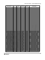
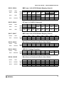
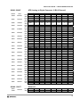
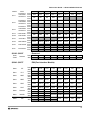
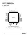
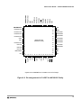
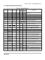
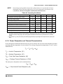
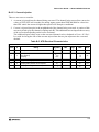
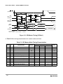
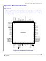
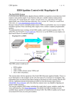
1
DOCUMENT NUMBER 9S12C128DGV1/D MC9S12C Family Device User Guide V01.05 Covers also MC9S12GC Family Original Release Date: 25 JAN 2003 Revised: 11 FEBRUARY 2004 Motorola, Inc. Motorola reserves the right to make changes without further notice to any products herein. Motorola makes no warranty, representation or guarantee regarding the suitability of its products for any particular purpose, nor does Motorola assume any liability arising out of the application or use of any product or circuit, and specifically disclaims any and all liability, including without limitation consequential or incidental damages. “Typical” parameters which may be provided in Motorola data sheets and/or specifications can and do vary in different applications and actual performance may vary over time. All operating parameters, including “Typicals” must be validated for each customer application by customer’s technical experts. Motorola does not convey any license under its patent rights nor the rights of others. Motorola products are not designed, intended, or authorized for use as components in systems intended for surgical implant into the body, or other applications intended to support or sustain life, or for any other application in which the failure of the Motorola product could create a situation where personal injury or death may occur. Should Buyer purchase or use Motorola products for any such unintended or unauthorized application, Buyer shall indemnify and hold Motorola and its officers, employees, subsidiaries, affiliates, and distributors harmless against all claims, costs, damages, and expenses, and reasonable attorney fees arising out of, directly or indirectly, any claim of personal injury or death associated with such unintended or unauthorized use, even if such claim alleges that Motorola was negligent regarding the design or manufacture of the part. Motorola and are registered trademarks of Motorola, Inc. Motorola, Inc. is an Equal Opportunity/Affirmative Action Employer. ©Motorola, Inc., 2002 1 Device User Guide — 9S12C128DGV1/D V01.05 Revision History Version Revision Effective Number Date Date 00.01 Author Description of Changes 25.JAN.03 25.JAN.03 Original Version. Based on C32 user guide version 01.12 00.02 07.FEB.03 07.FEB.03 Enhanced PortK description Part number table revision in preface 00.03 25.FEB.03 25.FEB.03 QFP112 Emulation pinout correction Enhanced part number explanation in preface Reduced pseudo STOP current spec. for C64,C96,C128 00.04 15.APR.03 15.APR03 Enhanced PortAD signal description Corrected VDDR description in 2.4.2 Revised pin leakage in electrical parameters 00.05 05.MAY.03 05.MAY.03 SPI timing parameter table correction Output drive high value reduced in 3V range PE[4:2] Pull-Up spec out of reset changed 3V Expansion bus timing parameters not tested in production Minimum bus frequency specification increased to 0.25MHz. 00.06 21.MAY.03 21.MAY.03 Parameter classification added to Appendix Table C-2. IOH changed to 4mA for 3V range. 01.00 15.JUL.03 LVR level defined.for C32. Run IDD changed for C32. Block guide reference table updated Added PCB layout guide for Pierce oscillator configuration IOL parameter updated in 3.3V range 01.01 12.AUG.03 12.AUG.03 Updated PARTID listing due to C128 ECO revision 01.02 20.NOV.03 20.NOV.03 Changed DOC number and CPU DOC reference number Included separate C32 LVI levels Changed PortM pull up reset state to enabled. 01.03 27.NOV.03 27.NOV.03 Added References to the CAN-less GC-Family No major revision number increment, since silicon functionality is not changed. Added VDDX connection in PCB layout figures 8-1.to 8-6 Added Part ID for 2L45J mask set to Part ID table 01.04 27.JAN.04 27.JAN.04 Table A-4 VDD/VDDPLL min when supplied externally now 2.35V Reference S12FTS128K1 in Preface (was S12FTS128K) Reference to CPU Guide corrected to Version2 11.FEB.04 11.FEB.04 Corrected flash sector sizes for C-Family devices with >64K Flash Corrected Preface Table 0-1 16K part listing to GC16 without CAN Added PPAGE specifications to memory map diagrams Added flash timing parameters for 1024 byte sector size 01.05 15.JUL03 2 Device User Guide — 9S12C128DGV1/D V01.05 Table of Contents Section 1 Introduction 1.1 1.2 1.3 1.4 1.5 1.6 1.7 Overview. . . . . . . . . . . . . . . . . . . . . . . . . . . . . . . . . . . . . . . . . . . . . . . . . . . . . . . . . . 23 Features . . . . . . . . . . . . . . . . . . . . . . . . . . . . . . . . . . . . . . . . . . . . . . . . . . . . . . . . . . 23 Modes of Operation . . . . . . . . . . . . . . . . . . . . . . . . . . . . . . . . . . . . . . . . . . . . . . . . . 25 Block Diagram . . . . . . . . . . . . . . . . . . . . . . . . . . . . . . . . . . . . . . . . . . . . . . . . . . . . . 27 Device Memory Map. . . . . . . . . . . . . . . . . . . . . . . . . . . . . . . . . . . . . . . . . . . . . . . . . 28 Detailed Register Map . . . . . . . . . . . . . . . . . . . . . . . . . . . . . . . . . . . . . . . . . . . . . . . 33 Part ID Assignments. . . . . . . . . . . . . . . . . . . . . . . . . . . . . . . . . . . . . . . . . . . . . . . . . 50 Section 2 Signal Description 2.1 Device Pinout . . . . . . . . . . . . . . . . . . . . . . . . . . . . . . . . . . . . . . . . . . . . . . . . . . . . . . 52 2.2 Signal Properties Summary . . . . . . . . . . . . . . . . . . . . . . . . . . . . . . . . . . . . . . . . . . . 55 2.2.1 Pin Initialization for 48 & 52 Pin LQFP bond-out versions . . . . . . . . . . . . . . . . . . 56 2.3 Detailed Signal Descriptions. . . . . . . . . . . . . . . . . . . . . . . . . . . . . . . . . . . . . . . . . . . 57 2.3.1 EXTAL, XTAL — Oscillator Pins . . . . . . . . . . . . . . . . . . . . . . . . . . . . . . . . . . . . . 57 2.3.2 RESET — External Reset Pin . . . . . . . . . . . . . . . . . . . . . . . . . . . . . . . . . . . . . . . 57 2.3.3 TEST / VPP — Test Pin . . . . . . . . . . . . . . . . . . . . . . . . . . . . . . . . . . . . . . . . . . . . 57 2.3.4 XFC — PLL Loop Filter Pin . . . . . . . . . . . . . . . . . . . . . . . . . . . . . . . . . . . . . . . . . 57 2.3.5 BKGD / TAGHI / MODC — Background Debug, Tag High & Mode Pin . . . . . . . 58 2.3.6 PA[7:0] / ADDR[15:8] / DATA[15:8] — Port A I/O Pins . . . . . . . . . . . . . . . . . . . . 58 2.3.7 PB[7:0] / ADDR[7:0] / DATA[7:0] — Port B I/O Pins . . . . . . . . . . . . . . . . . . . . . . 58 2.3.8 PE7 / NOACC / XCLKS — Port E I/O Pin 7 . . . . . . . . . . . . . . . . . . . . . . . . . . . . . 58 2.3.9 PE6 / MODB / IPIPE1 — Port E I/O Pin 6 . . . . . . . . . . . . . . . . . . . . . . . . . . . . . . 60 2.3.10 PE5 / MODA / IPIPE0 — Port E I/O Pin 5 . . . . . . . . . . . . . . . . . . . . . . . . . . . . . . 60 2.3.11 PE4 / ECLK— Port E I/O Pin [4] / E-Clock Output . . . . . . . . . . . . . . . . . . . . . . . . 60 2.3.12 PE3 / LSTRB — Port E I/O Pin [3] / Low-Byte Strobe (LSTRB). . . . . . . . . . . . . . 60 2.3.13 PE2 / R/W — Port E I/O Pin [2] / Read/Write. . . . . . . . . . . . . . . . . . . . . . . . . . . . 60 2.3.14 PE1 / IRQ — Port E input Pin [1] / Maskable Interrupt Pin . . . . . . . . . . . . . . . . . 61 2.3.15 PE0 / XIRQ — Port E input Pin [0] / Non Maskable Interrupt Pin . . . . . . . . . . . . 61 2.3.16 PAD[7:0] / AN[7:0] — Port AD I/O Pins [7:0] . . . . . . . . . . . . . . . . . . . . . . . . . . . . 61 2.3.17 PP[7] / KWP[7] — Port P I/O Pin [7]. . . . . . . . . . . . . . . . . . . . . . . . . . . . . . . . . . . 61 2.3.18 PP[6] / KWP[6]/ROMCTL — Port P I/O Pin [6] . . . . . . . . . . . . . . . . . . . . . . . . . . 61 2.3.19 PP[5:0] / KWP[5:0] / PW[5:0] — Port P I/O Pins [5:0] . . . . . . . . . . . . . . . . . . . . . 62 3 Device User Guide — 9S12C128DGV1/D V01.05 2.3.20 PJ[7:6] / KWJ[7:6] — Port J I/O Pins [7:6] . . . . . . . . . . . . . . . . . . . . . . . . . . . . . . 62 2.3.21 PM5 / SCK — Port M I/O Pin 5 . . . . . . . . . . . . . . . . . . . . . . . . . . . . . . . . . . . . . . 62 2.3.22 PM4 / MOSI — Port M I/O Pin 4 . . . . . . . . . . . . . . . . . . . . . . . . . . . . . . . . . . . . . 62 2.3.23 PM3 / SS — Port M I/O Pin 3. . . . . . . . . . . . . . . . . . . . . . . . . . . . . . . . . . . . . . . . 62 2.3.24 PM2 / MISO — Port M I/O Pin 2 . . . . . . . . . . . . . . . . . . . . . . . . . . . . . . . . . . . . . 62 2.3.25 PM1 / TXCAN — Port M I/O Pin 1 . . . . . . . . . . . . . . . . . . . . . . . . . . . . . . . . . . . . 62 2.3.26 PM0 / RXCAN — Port M I/O Pin 0 . . . . . . . . . . . . . . . . . . . . . . . . . . . . . . . . . . . . 62 2.3.27 PS[3:2] — Port S I/O Pins [3:2] . . . . . . . . . . . . . . . . . . . . . . . . . . . . . . . . . . . . . . 63 2.3.28 PS1 / TXD — Port S I/O Pin 1 . . . . . . . . . . . . . . . . . . . . . . . . . . . . . . . . . . . . . . . 63 2.3.29 PS0 / RXD — Port S I/O Pin 0 . . . . . . . . . . . . . . . . . . . . . . . . . . . . . . . . . . . . . . . 63 2.3.30 PPT[7:5] / IOC[7:5] — Port T I/O Pins [7:5] . . . . . . . . . . . . . . . . . . . . . . . . . . . . . 63 2.3.31 PT[4:0] / IOC[4:0] / PW[4:0]— Port T I/O Pins [4:0] . . . . . . . . . . . . . . . . . . . . . . . 63 2.4 Power Supply Pins . . . . . . . . . . . . . . . . . . . . . . . . . . . . . . . . . . . . . . . . . . . . . . . . . . 63 2.4.1 VDDX,VSSX — Power & Ground Pins for I/O Drivers . . . . . . . . . . . . . . . . . . . . . 63 2.4.2 VDDR, VSSR — Power & Ground Pins for I/O Drivers & for Internal Voltage Regulator 63 2.4.3 VDD1, VDD2, VSS1, VSS2 — Internal Logic Power Pins . . . . . . . . . . . . . . . . . . 63 2.4.4 VDDA, VSSA — Power Supply Pins for ATD and VREG . . . . . . . . . . . . . . . . . . 64 2.4.5 VRH, VRL — ATD Reference Voltage Input Pins . . . . . . . . . . . . . . . . . . . . . . . . 64 2.4.6 VDDPLL, VSSPLL — Power Supply Pins for PLL . . . . . . . . . . . . . . . . . . . . . . . . 64 Section 3 System Clock Description Section 4 Modes of Operation 4.1 4.2 4.3 4.3.1 4.3.2 4.3.3 4.4 4.4.1 4.4.2 4.4.3 4.4.4 Overview. . . . . . . . . . . . . . . . . . . . . . . . . . . . . . . . . . . . . . . . . . . . . . . . . . . . . . . . . . 65 Chip Configuration Summary . . . . . . . . . . . . . . . . . . . . . . . . . . . . . . . . . . . . . . . . . . 65 Security. . . . . . . . . . . . . . . . . . . . . . . . . . . . . . . . . . . . . . . . . . . . . . . . . . . . . . . . . . . 66 Securing the Microcontroller . . . . . . . . . . . . . . . . . . . . . . . . . . . . . . . . . . . . . . . . 67 Operation of the Secured Microcontroller . . . . . . . . . . . . . . . . . . . . . . . . . . . . . . 67 Unsecuring the Microcontroller . . . . . . . . . . . . . . . . . . . . . . . . . . . . . . . . . . . . . . 67 Low Power Modes . . . . . . . . . . . . . . . . . . . . . . . . . . . . . . . . . . . . . . . . . . . . . . . . . . 67 Stop . . . . . . . . . . . . . . . . . . . . . . . . . . . . . . . . . . . . . . . . . . . . . . . . . . . . . . . . . . . 68 Pseudo Stop. . . . . . . . . . . . . . . . . . . . . . . . . . . . . . . . . . . . . . . . . . . . . . . . . . . . . 68 Wait . . . . . . . . . . . . . . . . . . . . . . . . . . . . . . . . . . . . . . . . . . . . . . . . . . . . . . . . . . . 68 Run. . . . . . . . . . . . . . . . . . . . . . . . . . . . . . . . . . . . . . . . . . . . . . . . . . . . . . . . . . . . 68 Section 5 Resets and Interrupts 4 Device User Guide — 9S12C128DGV1/D V01.05 5.1 Overview. . . . . . . . . . . . . . . . . . . . . . . . . . . . . . . . . . . . . . . . . . . . . . . . . . . . . . . . . . 68 5.2 Vectors . . . . . . . . . . . . . . . . . . . . . . . . . . . . . . . . . . . . . . . . . . . . . . . . . . . . . . . . . . . 68 5.2.1 Vector Table. . . . . . . . . . . . . . . . . . . . . . . . . . . . . . . . . . . . . . . . . . . . . . . . . . . . . 68 5.3 Resets . . . . . . . . . . . . . . . . . . . . . . . . . . . . . . . . . . . . . . . . . . . . . . . . . . . . . . . . . . . 69 5.3.1 Reset Summary Table . . . . . . . . . . . . . . . . . . . . . . . . . . . . . . . . . . . . . . . . . . . . . 70 5.3.2 Effects of Reset . . . . . . . . . . . . . . . . . . . . . . . . . . . . . . . . . . . . . . . . . . . . . . . . . . 70 Section 6 HCS12 Core Block Description 6.1 Device-specific information. . . . . . . . . . . . . . . . . . . . . . . . . . . . . . . . . . . . . . . . . . . . 70 6.1.1 PPAGE. . . . . . . . . . . . . . . . . . . . . . . . . . . . . . . . . . . . . . . . . . . . . . . . . . . . . . . . . 70 6.1.2 BDM alternate clock . . . . . . . . . . . . . . . . . . . . . . . . . . . . . . . . . . . . . . . . . . . . . . . 71 6.1.3 Extended Address Range Emulation Implications . . . . . . . . . . . . . . . . . . . . . . . . 71 Section 7 Voltage Regulator (VREG) Block Description 7.1 Device-specific information. . . . . . . . . . . . . . . . . . . . . . . . . . . . . . . . . . . . . . . . . . . . 72 7.1.1 VREGEN . . . . . . . . . . . . . . . . . . . . . . . . . . . . . . . . . . . . . . . . . . . . . . . . . . . . . . . 72 7.1.2 VDD1, VDD2, VSS1, VSS2 . . . . . . . . . . . . . . . . . . . . . . . . . . . . . . . . . . . . . . . . . 72 Section 8 Recommended Printed Circuit Board Layout Section 9 Clock Reset Generator (CRG) Block Description 9.1 Device-specific information. . . . . . . . . . . . . . . . . . . . . . . . . . . . . . . . . . . . . . . . . . . . 79 9.1.1 XCLKS . . . . . . . . . . . . . . . . . . . . . . . . . . . . . . . . . . . . . . . . . . . . . . . . . . . . . . . . 80 Section 10 Oscillator (OSC) Block Description Section 11 Timer (TIM) Block Description Section 12 Analog to Digital Converter (ATD) Block Description 12.1 Device-specific information. . . . . . . . . . . . . . . . . . . . . . . . . . . . . . . . . . . . . . . . . . . . 80 12.1.1 VRL (voltage reference low). . . . . . . . . . . . . . . . . . . . . . . . . . . . . . . . . . . . . . . . . 80 Section 13 Serial Communications Interface (SCI) Block Description Section 14 Serial Peripheral Interface (SPI) Block Description Section 15 Flash Block Description 5 Device User Guide — 9S12C128DGV1/D V01.05 Section 16 RAM Block Description Section 17 Pulse Width Modulator (PWM) Block Description Section 18 MSCAN Block Description Section 19 Port Integration Module (PIM) Block Description Appendix A Electrical Characteristics A.1 General. . . . . . . . . . . . . . . . . . . . . . . . . . . . . . . . . . . . . . . . . . . . . . . . . . . . . . . . . . . 83 A.1.1 Parameter Classification . . . . . . . . . . . . . . . . . . . . . . . . . . . . . . . . . . . . . . . . . . . 83 A.1.2 Power Supply . . . . . . . . . . . . . . . . . . . . . . . . . . . . . . . . . . . . . . . . . . . . . . . . . . . . 83 A.1.3 Pins . . . . . . . . . . . . . . . . . . . . . . . . . . . . . . . . . . . . . . . . . . . . . . . . . . . . . . . . . . . 84 A.1.4 Current Injection. . . . . . . . . . . . . . . . . . . . . . . . . . . . . . . . . . . . . . . . . . . . . . . . . . 84 A.1.5 Absolute Maximum Ratings . . . . . . . . . . . . . . . . . . . . . . . . . . . . . . . . . . . . . . . . . 85 A.1.6 ESD Protection and Latch-up Immunity . . . . . . . . . . . . . . . . . . . . . . . . . . . . . . . . 86 A.1.7 Operating Conditions . . . . . . . . . . . . . . . . . . . . . . . . . . . . . . . . . . . . . . . . . . . . . . 86 A.1.8 Power Dissipation and Thermal Characteristics . . . . . . . . . . . . . . . . . . . . . . . . . 87 A.1.9 I/O Characteristics . . . . . . . . . . . . . . . . . . . . . . . . . . . . . . . . . . . . . . . . . . . . . . . . 89 A.1.10 Supply Currents . . . . . . . . . . . . . . . . . . . . . . . . . . . . . . . . . . . . . . . . . . . . . . . . . . 92 Appendix B Electrical Specifications B.1 B.2 B.3 B.3.1 B.3.2 B.4 B.4.1 B.4.2 B.4.3 B.4.4 B.4.5 B.5 B.5.1 B.5.2 6 Voltage Regulator Operating Conditions . . . . . . . . . . . . . . . . . . . . . . . . . . . . . . . . . 95 Chip Power-up and LVI/LVR graphical explanation . . . . . . . . . . . . . . . . . . . . . . . . . 96 Output Loads . . . . . . . . . . . . . . . . . . . . . . . . . . . . . . . . . . . . . . . . . . . . . . . . . . . . . . 96 Resistive Loads . . . . . . . . . . . . . . . . . . . . . . . . . . . . . . . . . . . . . . . . . . . . . . . . . . 96 Capacitive Loads . . . . . . . . . . . . . . . . . . . . . . . . . . . . . . . . . . . . . . . . . . . . . . . . . 97 ATD Characteristics . . . . . . . . . . . . . . . . . . . . . . . . . . . . . . . . . . . . . . . . . . . . . . . . . 99 ATD Operating Characteristics In 5V Range . . . . . . . . . . . . . . . . . . . . . . . . . . . . 99 ATD Operating Characteristics In 3.3V Range . . . . . . . . . . . . . . . . . . . . . . . . . . 99 Factors influencing accuracy. . . . . . . . . . . . . . . . . . . . . . . . . . . . . . . . . . . . . . . 100 ATD accuracy (5V Range) . . . . . . . . . . . . . . . . . . . . . . . . . . . . . . . . . . . . . . . . . 102 ATD accuracy (3.3V Range) . . . . . . . . . . . . . . . . . . . . . . . . . . . . . . . . . . . . . . . 102 NVM, Flash and EEPROM . . . . . . . . . . . . . . . . . . . . . . . . . . . . . . . . . . . . . . . . . . . 105 NVM timing. . . . . . . . . . . . . . . . . . . . . . . . . . . . . . . . . . . . . . . . . . . . . . . . . . . . . 105 NVM Reliability. . . . . . . . . . . . . . . . . . . . . . . . . . . . . . . . . . . . . . . . . . . . . . . . . . 106 Device User Guide — 9S12C128DGV1/D V01.05 B.6 Reset, Oscillator and PLL. . . . . . . . . . . . . . . . . . . . . . . . . . . . . . . . . . . . . . . . . . . . 109 B.6.1 Startup . . . . . . . . . . . . . . . . . . . . . . . . . . . . . . . . . . . . . . . . . . . . . . . . . . . . . . . . 109 B.6.2 Oscillator . . . . . . . . . . . . . . . . . . . . . . . . . . . . . . . . . . . . . . . . . . . . . . . . . . . . . . 110 B.6.3 Phase Locked Loop . . . . . . . . . . . . . . . . . . . . . . . . . . . . . . . . . . . . . . . . . . . . . . 111 B.7 MSCAN. . . . . . . . . . . . . . . . . . . . . . . . . . . . . . . . . . . . . . . . . . . . . . . . . . . . . . . . . . 117 B.8 SPI . . . . . . . . . . . . . . . . . . . . . . . . . . . . . . . . . . . . . . . . . . . . . . . . . . . . . . . . . . . . . 119 Appendix C Electrical Specifications C.1 Master Mode. . . . . . . . . . . . . . . . . . . . . . . . . . . . . . . . . . . . . . . . . . . . . . . . . . . . . . 119 C.2 Slave Mode. . . . . . . . . . . . . . . . . . . . . . . . . . . . . . . . . . . . . . . . . . . . . . . . . . . . . . . 121 C.3 External Bus Timing . . . . . . . . . . . . . . . . . . . . . . . . . . . . . . . . . . . . . . . . . . . . . . . . 123 C.3.1 General Muxed Bus Timing . . . . . . . . . . . . . . . . . . . . . . . . . . . . . . . . . . . . . . . . 123 Appendix D Package Information D.1 D.2 D.3 D.4 General. . . . . . . . . . . . . . . . . . . . . . . . . . . . . . . . . . . . . . . . . . . . . . . . . . . . . . . . . . 127 80-pin QFP package. . . . . . . . . . . . . . . . . . . . . . . . . . . . . . . . . . . . . . . . . . . . . . . . 128 52-pin LQFP package. . . . . . . . . . . . . . . . . . . . . . . . . . . . . . . . . . . . . . . . . . . . . . . 129 48-pin LQFP package. . . . . . . . . . . . . . . . . . . . . . . . . . . . . . . . . . . . . . . . . . . . . . . 130 Appendix E Emulation Information E.1 General. . . . . . . . . . . . . . . . . . . . . . . . . . . . . . . . . . . . . . . . . . . . . . . . . . . . . . . . . . 131 E.1.1 PK[2:0] / XADDR[16:14]. . . . . . . . . . . . . . . . . . . . . . . . . . . . . . . . . . . . . . . . . . . 132 E.2 112-pin LQFP package. . . . . . . . . . . . . . . . . . . . . . . . . . . . . . . . . . . . . . . . . . . . . . 133 7 Device User Guide — 9S12C128DGV1/D V01.05 8 Device User Guide — 9S12C128DGV1/D V01.05 List of Figures Figure 0-1 Figure 1-1 Figure 1-2 Figure 1-3 Figure 1-4 Figure 1-5 Figure 1-6 Figure 2-1 Figure 2-2 Figure 2-3 Figure 2-4 Figure 2-5 Figure 2-6 Figure 2-7 Figure 3-1 Figure 8-1 Figure 8-2 Figure 8-3 Figure 8-4 Figure 8-5 Figure 8-6 Figure B-1 Figure B-2 Figure B-3 Figure B-4 Figure B-5 Figure C-1 Figure C-2 Figure C-3 Figure C-4 Figure C-5 Figure D-1 Figure D-2 Order Part number Coding . . . . . . . . . . . . . . . . . . . . . . . . . . . . . . . . . . . . . . 16 MC9S12C-Family Block Diagram . . . . . . . . . . . . . . . . . . . . . . . . . . . . . . . . . 27 MC9S12C128 and MC9S12GC128 User configurable Memory Map . . . . . . 29 MC9S12C96 User Configurable Memory Map . . . . . . . . . . . . . . . . . . . . . . . 30 MC9S12C64 and MC9S12GC64 User Configurable Memory Map. . . . . . . . 31 MC9S12C32 and MC9S12GC32 User Configurable Memory Map. . . . . . . . 32 MC9S12GC16 User Configurable Memory Map . . . . . . . . . . . . . . . . . . . . . . 33 Pin Assignments in 80 QFP for MC9S12C-Family . . . . . . . . . . . . . . . . . . . . 52 Pin assignments in 52 LQFP for MC9S12C-Family. . . . . . . . . . . . . . . . . . . . 53 Pin Assignments in 48 LQFP for MC9S12C-Family . . . . . . . . . . . . . . . . . . . 54 PLL Loop Filter Connections . . . . . . . . . . . . . . . . . . . . . . . . . . . . . . . . . . . . . 57 Colpitts Oscillator Connections (PE7=1) . . . . . . . . . . . . . . . . . . . . . . . . . . . . 59 Pierce Oscillator Connections (PE7=0) . . . . . . . . . . . . . . . . . . . . . . . . . . . . . 59 External Clock Connections (PE7=0) . . . . . . . . . . . . . . . . . . . . . . . . . . . . . . 59 Clock Connections. . . . . . . . . . . . . . . . . . . . . . . . . . . . . . . . . . . . . . . . . . . . . 65 Recommended PCB Layout (48 LQFP) . . . . . . . . . . . . . . . . . . . . . . . . . . . . 74 Recommended PCB Layout (52 LQFP) . . . . . . . . . . . . . . . . . . . . . . . . . . . . 75 Recommended PCB Layout (80 QFP) . . . . . . . . . . . . . . . . . . . . . . . . . . . . . 76 Recommended PCB Layout for 48 LQFP Pierce Oscillator . . . . . . . . . . . . . 77 Recommended PCB Layout for 52 LQFP Pierce Oscillator . . . . . . . . . . . . . 78 Recommended PCB Layout for 80QFP Pierce Oscillator . . . . . . . . . . . . . . . 79 Voltage Regulator - Chip Power-up and Voltage Drops (not scaled) . . . . . 96 ATD Accuracy Definitions . . . . . . . . . . . . . . . . . . . . . . . . . . . . . . . . . . . . . 104 Basic PLL functional diagram . . . . . . . . . . . . . . . . . . . . . . . . . . . . . . . . . . 112 Jitter Definitions . . . . . . . . . . . . . . . . . . . . . . . . . . . . . . . . . . . . . . . . . . . . . 114 Maximum bus clock jitter approximation . . . . . . . . . . . . . . . . . . . . . . . . . . 114 SPI Master Timing (CPHA=0) . . . . . . . . . . . . . . . . . . . . . . . . . . . . . . . . . . 119 SPI Master Timing (CPHA=1) . . . . . . . . . . . . . . . . . . . . . . . . . . . . . . . . . . 120 SPI Slave Timing (CPHA=0) . . . . . . . . . . . . . . . . . . . . . . . . . . . . . . . . . . . 121 SPI Slave Timing (CPHA=1) . . . . . . . . . . . . . . . . . . . . . . . . . . . . . . . . . . . 122 General External Bus Timing. . . . . . . . . . . . . . . . . . . . . . . . . . . . . . . . . . . 123 80-pin QFP Mechanical Dimensions (case no. 841B) . . . . . . . . . . . . . . . . 128 52-pin LQFP Mechanical Dimensions (case no. 848D-03) . . . . . . . . . . . . 129 9 Device User Guide — 9S12C128DGV1/D V01.05 Figure D-3 48-pin LQFP Mechanical Dimensions (case no.932-03 ISSUE F) . . . . . . 130 Figure 19-1 Pin Assignments in 112-pin LQFP. . . . . . . . . . . . . . . . . . . . . . . . . . . . . . . . 131 Figure 19-2 112-pin LQFP mechanical dimensions (case no. 987)80-pin QFP Mechanical Dimensions (case no. 841B)133 10 Device User Guide — 9S12C128DGV1/D V01.05 List of Tables Table 0-2 MC9S12C-Family Package Option Summary . . . . . . . . . . . . . . . . . . . . . . . . . 15 Table 0-1 List of MC9S12C and MC9S12GC Family members. . . . . . . . . . . . . . . . . . . . 15 Table 0-3 MC9S12C-Family Part Number Coding. . . . . . . . . . . . . . . . . . . . . . . . . . . . . . 16 Table 0-4 MC9S12GC-Family Part Number Coding . . . . . . . . . . . . . . . . . . . . . . . . . . . . 19 Table 0-5 Document References . . . . . . . . . . . . . . . . . . . . . . . . . . . . . . . . . . . . . . . . . . 21 Table 1-1 Device Register Map Overview . . . . . . . . . . . . . . . . . . . . . . . . . . . . . . . . . . . . 28 $0000 - $000FMEBI map 1 of 3 (HCS12 Multiplexed External Bus Interface) 34 $0010 - $0014 MMC map 1 of 4 (HCS12 Module Mapping Control) 34 $0018 - $0018 Miscellaneous Peripherals (Device User Guide) 35 $0019 - $0019 VREG3V3 (Voltage Regulator) 35 $0015 - $0016 INT map 1 of 2 (HCS12 Interrupt) 35 $0017 - $0017MMC map 2 of 4 (HCS12 Module Mapping Control) 35 $001A - $001B Miscellaneous Peripherals (Device User Guide) 35 $001C - $001D MMC map 3 of 4 (HCS12 Module Mapping Control, 36 Device User Guide) 36 $001E - $001E MEBI map 2 of 3 (HCS12 Multiplexed External Bus Interface) 36 $001F - $001F INT map 2 of 2 (HCS12 Interrupt) 36 $0020 - $002F DBG (including BKP) map 1 of 1 (HCS12 Debug) 36 $0030 - $0031 MMC map 4 of 4 (HCS12 Module Mapping Control) 37 $0032 - $0033 MEBI map 3 of 3 (HCS12 Multiplexed External Bus Interface) 37 $0034 - $003F CRG (Clock and Reset Generator) 37 $0040 - $006F TIM (Timer 16 Bit 8 Channels) 38 $0070 - $007F Reserved 40 $0080 - $009F ATD (Analog to Digital Converter 10 Bit 8 Channel) 40 $00A0 - $00C7 Reserved 41 $00D0 - $00D7 Reserved 42 $00C8 - $00CF SCI (Asynchronous Serial Interface) 42 $00D8 - $00DF SPI (Serial Peripheral Interface) 42 $00E0 - $00FF PWM (Pulse Width Modulator) 43 $0100 - $010F Flash Control Register 44 $0110 - $013F Reserved 45 $0140 - $017F CAN (Motorola Scalable CAN - MSCAN) 45 Table 1-2 Detailed MSCAN Foreground Receive and Transmit Buffer Layout. . . . . . . . 46 11 Device User Guide — 9S12C128DGV1/D V01.05 $0180 - $023F Reserved 47 $0240 - $027F PIM (Port Interface Module) 47 $0280 - $03FF Reserved space 50 Table 1-3 Assigned Part ID Numbers . . . . . . . . . . . . . . . . . . . . . . . . . . . . . . . . . . . . . . . 50 Table 1-4 Memory size registers . . . . . . . . . . . . . . . . . . . . . . . . . . . . . . . . . . . . . . . . . . . 50 Table 2-1 Signal Properties . . . . . . . . . . . . . . . . . . . . . . . . . . . . . . . . . . . . . . . . . . . . . . . 55 Table 2-2 MC9S12C-Family Power and Ground Connection Summary . . . . . . . . . . . . . 64 Table 4-1 Mode Selection . . . . . . . . . . . . . . . . . . . . . . . . . . . . . . . . . . . . . . . . . . . . . . . . 66 Table 4-2 Clock Selection Based on PE7 . . . . . . . . . . . . . . . . . . . . . . . . . . . . . . . . . . . . 66 Table 5-1 Interrupt Vector Locations . . . . . . . . . . . . . . . . . . . . . . . . . . . . . . . . . . . . . . . . 68 Table 5-2 Reset Summary . . . . . . . . . . . . . . . . . . . . . . . . . . . . . . . . . . . . . . . . . . . . . . . . 70 Table 6-1 Device Specific Flash PAGE Mapping. . . . . . . . . . . . . . . . . . . . . . . . . . . . . . . 71 Table 8-1 Recommended External Component Values. . . . . . . . . . . . . . . . . . . . . . . . . . 73 Table A-1 Absolute Maximum Ratings . . . . . . . . . . . . . . . . . . . . . . . . . . . . . . . . . . . . . . . 85 Table A-2 ESD and Latch-up Test Conditions . . . . . . . . . . . . . . . . . . . . . . . . . . . . . . . . . 86 Table A-3 ESD and Latch-Up Protection Characteristics . . . . . . . . . . . . . . . . . . . . . . . . . 86 Table A-4 Operating Conditions . . . . . . . . . . . . . . . . . . . . . . . . . . . . . . . . . . . . . . . . . . . . 87 Table A-5 Thermal Package Characteristics . . . . . . . . . . . . . . . . . . . . . . . . . . . . . . . . . . 89 Table A-6 5V I/O Characteristics . . . . . . . . . . . . . . . . . . . . . . . . . . . . . . . . . . . . . . . . . . . 90 Table A-7 3.3V I/O Characteristics . . . . . . . . . . . . . . . . . . . . . . . . . . . . . . . . . . . . . . . . . . 91 Table A-8 Supply Current Characteristics for MC9S12C32 . . . . . . . . . . . . . . . . . . . . . . . 93 Table A-9 Supply Current Characteristics for MC9S12C64,MC9S12C96,MC9S12C128 94 Table B-1 Voltage Regulator Electrical Parameters . . . . . . . . . . . . . . . . . . . . . . . . . . . . 95 Table B-2 Voltage Regulator - Capacitive Loads . . . . . . . . . . . . . . . . . . . . . . . . . . . . . . . 97 Table B-3 ATD Operating Characteristics . . . . . . . . . . . . . . . . . . . . . . . . . . . . . . . . . . . . 99 Table B-4 ATD Operating Characteristics . . . . . . . . . . . . . . . . . . . . . . . . . . . . . . . . . . . 100 Table B-5 ATD Electrical Characteristics . . . . . . . . . . . . . . . . . . . . . . . . . . . . . . . . . . . . 101 Table B-6 ATD Conversion Performance . . . . . . . . . . . . . . . . . . . . . . . . . . . . . . . . . . . 102 Table B-7 ATD Conversion Performance . . . . . . . . . . . . . . . . . . . . . . . . . . . . . . . . . . . 102 Table B-8 NVM Timing Characteristics . . . . . . . . . . . . . . . . . . . . . . . . . . . . . . . . . . . . . 106 Table B-9 NVM Reliability Characteristics. . . . . . . . . . . . . . . . . . . . . . . . . . . . . . . . . . . 107 Table B-10 Startup Characteristics. . . . . . . . . . . . . . . . . . . . . . . . . . . . . . . . . . . . . . . . . . 109 Table B-11 Oscillator Characteristics . . . . . . . . . . . . . . . . . . . . . . . . . . . . . . . . . . . . . . . . 111 Table B-12 PLL Characteristics . . . . . . . . . . . . . . . . . . . . . . . . . . . . . . . . . . . . . . . . . . . . 115 Table B-13 MSCAN Wake-up Pulse Characteristics. . . . . . . . . . . . . . . . . . . . . . . . . . . . 117 Table C-1 Measurement Conditions . . . . . . . . . . . . . . . . . . . . . . . . . . . . . . . . . . . . . . . . 119 12 Device User Guide — 9S12C128DGV1/D V01.05 Table C-2 Table C-3 Table C-4 Table C-5 SPI Master Mode Timing Characteristics. . . . . . . . . . . . . . . . . . . . . . . . . . . . 120 SPI Slave Mode Timing Characteristics. . . . . . . . . . . . . . . . . . . . . . . . . . . . . 122 Expanded Bus Timing Characteristics (5V Range). . . . . . . . . . . . . . . . . . . . 124 Expanded Bus Timing Characteristics (3.3V Range) . . . . . . . . . . . . . . . . . . 125 13 Device User Guide — 9S12C128DGV1/D V01.05 14 Device User Guide — 9S12C128DGV1/D V01.05 Preface The Device User Guide provides information about the MC9S12C-Family as well the MC9S12GC-Family devices made up of standard HCS12 blocks and the HCS12 processor core. This document is part of the customer documentation. A complete set of device manuals also includes the HCS12 Core User Guide and all the individual Block User Guides of the implemented modules. In an effort to reduce redundancy all module specific information is located only in the respective Block User Guide. If applicable, special implementation details of the module are given in the block description sections of this document. The C-Family and the GC-Family offer an extensive range of package, temperature and speed options. The members of the GC-Family do not feature a CAN module. Table 0-1 shows a feature overview of the MC9S12C and MC9S12GC Family members. Table 0-2 summarizes the package option and size configuration. Table 0-3 lists the part number coding based on the package, speed and temperature and preliminary die options for the C-Family. Table 0-4 lists the part number coding based on the package, speed and temperature and preliminary die options for the GC-Family. Table 0-1 List of MC9S12C and MC9S12GC Family members Flash RAM 128K 4K 96K 4K 64K 4K 32K 2K 16K 1K CAN SCI SPI A/D PWM Timer MC9S12C128 Device 1 1 1 8ch 6ch 8ch MC9S12GC128 — 1 1 8ch 6ch 8ch MC9S12C96 1 1 1 8ch 6ch 8ch MC9S12C64 1 1 1 8ch 6ch 8ch MC9S12GC64 — 1 1 8ch 6ch 8ch MC9S12C32 1 1 1 8ch 6ch 8ch MC9S12GC32 — 1 1 8ch 6ch 8ch MC9S12GC16 — 1 1 8ch 6ch 8ch Table 0-2 MC9S12C-Family Package Option Summary Package Device Part Number Mask1 set Temp.2 Options Flash RAM 128K 4K I/O3,4 48LQFP MC9S12C128 MC9S12C128 0L09S M, V, C 52LQFP MC9S12C128 MC9S12C128 0L09S M, V, C 80QFP MC9S12C128 MC9S12C128 0L09S M, V, C 60 48LQFP MC9S12C96 MC9S12C96 TBD M, V, C 31 52LQFP MC9S12C96 MC9S12C96 TBD M, V, C 80QFP MC9S12C96 MC9S12C96 TBD M, V, C 31 96K 4K 35 35 60 15 Device User Guide — 9S12C128DGV1/D V01.05 Package Device 48LQFP Part Number MC9S12C64 MC9S12C64 Mask1 set Temp.2 Options TBD M, V, C 52LQFP MC9S12C64 MC9S12C64 TBD M, V, C 80QFP MC9S12C64 MC9S12C64 TBD M, V, C 48LQFP MC9S12C32 MC9S12C32 1L45J M, V, C 52LQFP MC9S12C32 MC9S12C32 1L45J M, V, C Flash RAM I/O3,4 31 64K 4K 35 60 31 32K 2K 35 80QFP MC9S12C32 MC9S12C32 1L45J M, V, C 60 48LQFP MC9S12GC128 MC9S12GC128 0L09S M, V, C 31 52LQFP MC9S12GC128 MC9S12GC128 0L09S M, V, C 80QFP MC9S12GC128 MC9S12GC128 0L09S M, V, C 128K 4K 35 60 48LQFP MC9S12GC128 MC9S12GC64 TBD M, V, C 52LQFP MC9S12GC128 MC9S12GC64 TBD M, V, C 80QFP MC9S12GC128 MC9S12GC64 TBD M, V, C 60 48LQFP MC9S12GC32 MC9S12GC32 1L45J M, V, C 31 52LQFP MC9S12GC32 MC9S12GC32 1L45J M, V, C 80QFP MC9S12GC32 MC9S12GC32 1L45J M, V, C 48LQFP MC9S12GC16 MC9S12GC16 1L45J M, V, C 52LQFP MC9S12GC16 MC9S12GC16 1L45J M, V, C 80QFP MC9S12GC16 MC9S12GC16 1L45J M, V, C 31 64K 4K 32K 2K 35 35 60 31 16K 2K 35 60 NOTES: 1. Maskset dependent errata can be accessed at http://e-www.motorola.com/wbapp/sps/site/prod_summary.jsp 2. C: TA = 85˚C, f = 25MHz. V: TA=105˚C, f = 25MHz. M: TA= 125˚C, f = 25MHz 3. All C-Family derivatives feature 1 CAN, 1 SCI, 1 SPI, an 8-channel A/D, a 6-channel PWM and an 8 channel timer. The GC-Family members do not have the CAN module 4. I/O is the sum of ports capable to act as digital input or output. MC9S12 C32 (P)C FU 25 Speed Option Package Option Temperature Option Preliminary Option Device Title Controller Family Temperature Options C = -40˚C to 85˚C V = -40˚C to 105˚C M = -40˚C to 125˚C Package Options FU = 80QFP PB = 52LQFP FA = 48LQFP Speed Options 25 = 25MHz bus 16 = 16MHz bus Figure 0-1 Order Part number Coding Table 0-3 MC9S12C-Family Part Number Coding Part Number MC9S12C128CFA16 16 Mask set Temp. Package Speed Description TBD -40˚C, 85˚C 48LQFP 16MHz C128 die Device User Guide — 9S12C128DGV1/D V01.05 Mask set Temp. Package Speed Description MC9S12C128CPB16 TBD -40˚C, 85˚C 52LQFP 16MHz C128 die MC9S12C128CFU16 TBD -40˚C, 85˚C 80QFP 16MHz C128 die MC9S12C128VFA16 TBD -40˚C,105˚C 48LQFP 16MHz C128 die MC9S12C128VPB16 TBD -40˚C,105˚C 52LQFP 16MHz C128 die MC9S12C128VFU16 TBD -40˚C, 105˚C 80QFP 16MHz C128 die MC9S12C128MFA16 TBD -40˚C,125˚C 48LQFP 16MHz C128 die Part Number MC9S12C128MPB16 TBD -40˚C,125˚C 52LQFP 16MHz C128 die MC9S12C128MFU16 TBD -40˚C, 125˚C 80QFP 16MHz C128 die MC9S12C128CFA25 TBD -40˚C, 85˚C 48LQFP 25MHz C128 die MC9S12C128CPB25 TBD -40˚C, 85˚C 52LQFP 25MHz C128 die MC9S12C128CFU25 TBD -40˚C, 85˚C 80QFP 25MHz C128 die MC9S12C128VFA25 TBD -40˚C,105˚C 48LQFP 25MHz C128 die MC9S12C128VPB25 TBD -40˚C,105˚C 52LQFP 25MHz C128 die MC9S12C128VFU25 TBD -40˚C, 105˚C 80QFP 25MHz C128 die MC9S12C128MFA25 TBD -40˚C,125˚C 48LQFP 25MHz C128 die MC9S12C128MPB25 TBD -40˚C,125˚C 52LQFP 25MHz C128 die MC9S12C128MFU25 TBD -40˚C, 125˚C 80QFP 25MHz C128 die MC9S12C96PCFA16 0L09S -40˚C, 85˚C 48LQFP 16MHz Preliminary C96 using C128 die MC9S12C96PCPB16 0L09S -40˚C, 85˚C 52LQFP 16MHz Preliminary C96 using C128 die MC9S12C96PCFU16 0L09S -40˚C, 85˚C 80QFP 16MHz Preliminary C96 using C128 die MC9S12C96CFA16 TBD -40˚C, 85˚C 48LQFP 16MHz Final C96 using C96 die MC9S12C96CPB16 TBD -40˚C, 85˚C 52LQFP 16MHz Final C96 using C96 die MC9S12C96CFU16 TBD -40˚C, 85˚C 80QFP 16MHz Final C96 using C96 die MC9S12C96PVFA16 0L09S -40˚C, 105˚C 48LQFP 16MHz Preliminary C96 using C128 die MC9S12C96PVPB16 0L09S -40˚C, 105˚C 52LQFP 16MHz Preliminary C96 using C128 die MC9S12C96PVFU16 0L09S -40˚C, 105˚C 80QFP 16MHz Preliminary C96 using C128 die MC9S12C96VFA16 TBD -40˚C,105˚C 48LQFP 16MHz Final C96 using C96 die MC9S12C96VPB16 TBD -40˚C,105˚C 52LQFP 16MHz Final C96 using C96die TBD -40˚C, 105˚C 80QFP 16MHz Final C96 using C96 die MC9S12C96PMFA16 MC9S12C96VFU16 0L09S -40˚C, 125˚C 48LQFP 16MHz Preliminary C96 using C128 die MC9S12C96PMPB16 0L09S -40˚C, 125˚C 52LQFP 16MHz Preliminary C96 using C128 die MC9S12C96PMFU16 0L09S -40˚C, 125˚C 80QFP 16MHz Preliminary C96 using C128 die MC9S12C96MFA16 TBD -40˚C,125˚C 48LQFP 16MHz Final C96 using C96 die MC9S12C96MPB16 TBD -40˚C,125˚C 52LQFP 16MHz Final C96 using C96 die MC9S12C96MFU16 TBD -40˚C, 125˚C 80QFP 16MHz Final C96 using C96 die MC9S12C96PCFA25 0L09S -40˚C, 85˚C 48LQFP 25MHz Preliminary C96 using C128 die MC9S12C96PCPB25 0L09S -40˚C, 85˚C 52LQFP 25MHz Preliminary C96 using C128 die MC9S12C96PCFU25 0L09S -40˚C, 85˚C 80QFP 25MHz Preliminary C96 using C128 die MC9S12C96CFA25 TBD -40˚C, 85˚C 48LQFP 25MHz Final C96 using C96 die MC9S12C96CPB25 TBD -40˚C, 85˚C 52LQFP 25MHz Final C96 using C96 die MC9S12C96CFU25 TBD -40˚C, 85˚C 80QFP 25MHz Final C96 using C96 die MC9S12C96PVFA25 0L09S -40˚C, 105˚C 48LQFP 25MHz Preliminary C96 using C128 die MC9S12C96PVPB25 0L09S -40˚C, 105˚C 52LQFP 25MHz Preliminary C96 using C128 die MC9S12C96PVFU25 0L09S -40˚C, 105˚C 80QFP 25MHz Preliminary C96 using C128 die 17 Device User Guide — 9S12C128DGV1/D V01.05 Part Number Temp. Package Speed Description MC9S12C96VFA25 TBD -40˚C,105˚C 48LQFP 25MHz Final C96 using C96 die MC9S12C96VPB25 TBD -40˚C,105˚C 52LQFP 25MHz Final C96 using C96 die MC9S12C96VFU25 TBD -40˚C, 105˚C 80QFP 25MHz Final C96 using C96 die MC9S12C96PMFA25 0L09S -40˚C, 125˚C 48LQFP 25MHz Preliminary C96 using C128 die MC9S12C96PMPB25 0L09S -40˚C, 125˚C 52LQFP 25MHz Preliminary C96 using C128 die MC9S12C96PMFU25 0L09S -40˚C, 125˚C 80QFP 25MHz Preliminary C96 using C128 die MC9S12C96MFA25 TBD -40˚C,125˚C 48LQFP 25MHz Final C96 using C96 die MC9S12C96MPB25 TBD -40˚C,125˚C 52LQFP 25MHz Final C96 using C96 die MC9S12C96MFU25 TBD -40˚C, 125˚C 80QFP 25MHz Final C96 using C96 die MC9S12C64PCFA16 0L09S -40˚C, 85˚C 48LQFP 16MHz Preliminary C64 using C128 die MC9S12C64PCPB16 0L09S -40˚C, 85˚C 52LQFP 16MHz Preliminary C64 using C128 die MC9S12C64PCFU16 0L09S -40˚C, 85˚C 80QFP 16MHz Preliminary C64 using C128 die MC9S12C64CFA16 TBD -40˚C, 85˚C 48LQFP 16MHz Final C64 using C64 die MC9S12C64CPB16 TBD -40˚C, 85˚C 52LQFP 16MHz Final C64 using C64 die MC9S12C64CFU16 TBD -40˚C, 85˚C 80QFP 16MHz Final C64 using C64 die MC9S12C64PVFA16 0L09S -40˚C, 105˚C 48LQFP 16MHz Preliminary C64 using C128 die MC9S12C64PVPB16 0L09S -40˚C, 105˚C 52LQFP 16MHz Preliminary C64 using C128 die MC9S12C64PVFU16 0L09S -40˚C, 105˚C 80QFP 16MHz Preliminary C64 using C128 die MC9S12C64VFA16 TBD -40˚C,105˚C 48LQFP 16MHz Final C64 using C64 die MC9S12C64VPB16 TBD -40˚C,105˚C 52LQFP 16MHz Final C64 using C64 die MC9S12C64VFU16 TBD -40˚C, 105˚C 80QFP 16MHz Final C64 using C64 die MC9S12C64PMFA16 0L09S -40˚C, 125˚C 48LQFP 16MHz Preliminary C64 using C128 die MC9S12C64PMPB16 0L09S -40˚C, 125˚C 52LQFP 16MHz Preliminary C64 using C128 die MC9S12C64PMFU16 0L09S -40˚C, 125˚C 80QFP 16MHz Preliminary C64 using C128 die MC9S12C64MFA16 TBD -40˚C,125˚C 48LQFP 16MHz Final C64 using C64 die MC9S12C64MPB16 TBD -40˚C,125˚C 52LQFP 16MHz Final C64 using C64 die MC9S12C64MFU16 TBD -40˚C, 125˚C 80QFP 16MHz Final C64 using C64 die MC9S12C64PCFA25 0L09S -40˚C, 85˚C 48LQFP 25MHz Preliminary C64 using C128 die MC9S12C64PCPB25 0L09S -40˚C, 85˚C 52LQFP 25MHz Preliminary C64 using C128 die MC9S12C64PCFU25 0L09S -40˚C, 85˚C 80QFP 25MHz PreliminaryC64 using C128 die MC9S12C64CFA25 TBD -40˚C, 85˚C 48LQFP 25MHz Final C64 using C64 die MC9S12C64CPB25 TBD -40˚C, 85˚C 52LQFP 25MHz Final C64 using C64 die MC9S12C64CFU25 TBD -40˚C, 85˚C 80QFP 25MHz Final C64 using C64 die MC9S12C64PVFA25 0L09S -40˚C, 105˚C 48LQFP 25MHz Preliminary C64 using C128 die MC9S12C64PVPB25 0L09S -40˚C, 105˚C 52LQFP 25MHz Preliminary C64 using C128 die MC9S12C64PVFU25 0L09S -40˚C, 105˚C 80QFP 25MHz Preliminary C64 using C128 die MC9S12C64VFA25 TBD -40˚C,105˚C 48LQFP 25MHz Final C64 using C64 die MC9S12C64VPB25 TBD -40˚C,105˚C 52LQFP 25MHz Final C64 using C64 die MC9S12C64VFU25 18 Mask set TBD -40˚C, 105˚C 80QFP 25MHz Final C64 using C64 die MC9S12C64PMFA25 0L09S -40˚C, 125˚C 48LQFP 25MHz Preliminary C64 using C128 die MC9S12C64PMPB25 0L09S -40˚C, 125˚C 52LQFP 25MHz Preliminary C64 using C128 die MC9S12C64PMFU25 0L09S -40˚C, 125˚C 80QFP 25MHz Preliminary C64 using C128 die MC9S12C64MFA25 TBD -40˚C,125˚C 48LQFP 25MHz Final C64 using C64 die MC9S12C64MPB25 TBD -40˚C,125˚C 52LQFP 25MHz Final C64 using C64 die Device User Guide — 9S12C128DGV1/D V01.05 Mask set Temp. MC9S12C64MFU25 TBD MC9S12C32CFA16 1L45J MC9S12C32CPB16 MC9S12C32CFU16 Part Number Package Speed Description -40˚C, 125˚C 80QFP 25MHz Final C64 using C64 die -40˚C, 85˚C 48LQFP 16MHz C32 die 1L45J -40˚C, 85˚C 52LQFP 16MHz C32 die 1L45J -40˚C, 85˚C 80QFP 16MHz C32 die MC9S12C32VFA16 1L45J -40˚C,105˚C 48LQFP 16MHz C32 die MC9S12C32VPB16 1L45J -40˚C,105˚C 52LQFP 16MHz C32 die MC9S12C32VFU16 1L45J -40˚C, 105˚C 80QFP 16MHz C32 die MC9S12C32MFA16 1L45J -40˚C,125˚C 48LQFP 16MHz C32 die MC9S12C32MPB16 1L45J -40˚C,125˚C 52LQFP 16MHz C32 die MC9S12C32MFU16 1L45J -40˚C, 125˚C 80QFP 16MHz C32 die MC9S12C32CFA25 1L45J -40˚C, 85˚C 48LQFP 25MHz C32 die MC9S12C32CPB25 1L45J -40˚C, 85˚C 52LQFP 25MHz C32 die MC9S12C32CFU25 1L45J -40˚C, 85˚C 80QFP 25MHz C32 die MC9S12C32VFA25 1L45J -40˚C,105˚C 48LQFP 25MHz C32 die MC9S12C32VPB25 1L45J -40˚C,105˚C 52LQFP 25MHz C32 die MC9S12C32VFU25 1L45J -40˚C, 105˚C 80QFP 25MHz C32 die MC9S12C32MFA25 1L45J -40˚C,125˚C 48LQFP 25MHz C32 die MC9S12C32MPB25 1L45J -40˚C,125˚C 52LQFP 25MHz C32 die MC9S12C32MFU25 1L45J -40˚C, 125˚C 80QFP 25MHz C32 die Table 0-4 MC9S12GC-Family Part Number Coding Part Number Mask set Temp. Package Speed Description MC9S12GC128PCFA25 0L09S -40˚C, 85˚C 48LQFP 25MHz Preliminary GC128 using C128 die MC9S12GC128PCPB25 0L09S -40˚C, 85˚C 52LQFP 25MHz Preliminary GC128 using C128 die MC9S12GC128PCFU25 0L09S -40˚C, 85˚C 80QFP 25MHz Preliminary GC128 using C128 die MC9S12GC128CFA25 TBD -40˚C, 85˚C 48LQFP 25MHz Final GC128 using GC128 die MC9S12GC128CPB25 TBD -40˚C, 85˚C 52LQFP 25MHz Final GC128 using GC128 die MC9S12GC128CFU25 TBD -40˚C, 85˚C 80QFP 25MHz Final GC128 using GC128 die MC9S12GC128PVFA25 0L09S -40˚C, 105˚C 48LQFP 25MHz Preliminary GC128 using C128 die MC9S12GC128PVPB25 0L09S -40˚C, 105˚C 52LQFP 25MHz Preliminary GC128 using C128 die MC9S12GC128PVFU25 0L09S -40˚C, 105˚C 80QFP 25MHz Preliminary GC128 using C128 die MC9S12GC128VFA25 TBD -40˚C, 105˚C 48LQFP 25MHz Final GC128 using GC128 die MC9S12GC128VPB25 TBD -40˚C, 105˚C 52LQFP 25MHz Final GC128 using GC128 die MC9S12GC128VFU25 TBD -40˚C, 105˚C 80QFP 25MHz Final GC128 using GC128 die MC9S12GC128PMFA25 0L09S -40˚C, 125˚C 48LQFP 25MHz Preliminary GC128 using C128 die MC9S12GC128PMPB25 0L09S -40˚C, 125˚C 52LQFP 25MHz Preliminary GC128 using C128 die MC9S12GC128PMFU25 0L09S -40˚C, 125˚C 80QFP 25MHz Preliminary GC128 using C128 die MC9S12GC128MFA25 TBD -40˚C, 125˚C 48LQFP 25MHz Final GC128 using GC128 die MC9S12GC128MPB25 TBD -40˚C, 125˚C 52LQFP 25MHz Final GC128 using GC128 die MC9S12GC128MFU25 TBD -40˚C, 125˚C 80QFP 25MHz Final GC128 using GC128 die MC9S12GC64PCFA25 0L09S -40˚C, 85˚C 48LQFP 25MHz Preliminary GC64 using C128 die MC9S12GC64PCPB25 0L09S -40˚C, 85˚C 52LQFP 25MHz Preliminary GC64 using C128 die MC9S12GC64PCFU25 0L09S -40˚C, 85˚C 80QFP 25MHz Preliminary GC64 using C128 die 19 Device User Guide — 9S12C128DGV1/D V01.05 Mask set Temp. Package Speed Description MC9S12GC64CFA25 TBD -40˚C, 85˚C 48LQFP 25MHz Final GC64 using GC64 die MC9S12GC64CPB25 TBD -40˚C, 85˚C 52LQFP 25MHz Final GC64 using GC64 die Part Number MC9S12GC64CFU25 TBD -40˚C, 85˚C 80QFP 25MHz Final GC64 using GC64 die MC9S12GC64PVFA25 0L09S -40˚C, 105˚C 48LQFP 25MHz Preliminary GC64 using C128 die MC9S12GC64PVPB25 0L09S -40˚C, 105˚C 52LQFP 25MHz Preliminary GC64 using C128 die MC9S12GC64PVFU25 0L09S -40˚C, 105˚C 80QFP 25MHz Preliminary GC64 using C128 die MC9S12GC64VFA25 TBD -40˚C, 105˚C 48LQFP 25MHz Final GC64 using GC64 die MC9S12GC64VPB25 TBD -40˚C, 105˚C 52LQFP 25MHz Final GC64 using GC64 die TBD -40˚C, 105˚C 80QFP 25MHz Final GC64 using GC64 die MC9S12GC64PMFA25 MC9S12GC64VFU25 0L09S -40˚C, 125˚C 48LQFP 25MHz Preliminary GC64 using C128 die MC9S12GC64PMPB25 0L09S -40˚C, 125˚C 52LQFP 25MHz Preliminary GC64 using C128 die MC9S12GC64PMFU25 0L09S -40˚C, 125˚C 80QFP 25MHz Preliminary GC64 using C128 die MC9S12GC64MFA25 TBD -40˚C, 125˚C 48LQFP 25MHz Final GC64 using GC64 die MC9S12GC64MPB25 TBD -40˚C, 125˚C 52LQFP 25MHz Final GC64 using GC64 die MC9S12GC64MFU25 TBD -40˚C, 125˚C 80QFP 25MHz Final GC64 using GC64 die MC9S12GC32PCFA25 1L45J -40˚C, 85˚C 48LQFP 25MHz Preliminary GC32 using C32 die MC9S12GC32PCPB25 1L45J -40˚C, 85˚C 52LQFP 25MHz Preliminary GC32 using C32 die MC9S12GC32PCFU25 1L45J -40˚C, 85˚C 80QFP 25MHz Preliminary GC32 using C32 die MC9S12GC32CFA25 TBD -40˚C, 85˚C 48LQFP 25MHz Final GC32 using GC32 die MC9S12GC32CPB25 TBD -40˚C, 85˚C 52LQFP 25MHz Final GC32 using GC32 die MC9S12GC32CFU25 TBD -40˚C, 85˚C 80QFP 25MHz Final GC32 using GC32 die MC9S12GC32PVFA25 1L45J -40˚C,105˚C 48LQFP 25MHz Preliminary GC32 using C32 die MC9S12GC32PVPB25 1L45J -40˚C,105˚C 52LQFP 25MHz Preliminary GC32 using C32 die MC9S12GC32PVFU25 1L45J -40˚C, 105˚C 80QFP 25MHz Preliminary GC32 using C32 die MC9S12GC32VFA25 TBD -40˚C,105˚C 48LQFP 25MHz Final GC32 using GC32 die MC9S12GC32VPB25 TBD -40˚C,105˚C 52LQFP 25MHz Final GC32 using GC32 die MC9S12GC32VFU25 20 TBD -40˚C, 105˚C 80QFP 25MHz Final GC32 using GC32 die MC9S12GC32PMFA25 1L45J -40˚C,125˚C 48LQFP 25MHz Preliminary GC32 using C32 die MC9S12GC32PMPB25 1L45J -40˚C,125˚C 52LQFP 25MHz Preliminary GC32 using C32 die MC9S12GC32PMFU25 1L45J -40˚C, 125˚C 80QFP 25MHz Preliminary GC32 using C32 die MC9S12GC32MFA25 TBD -40˚C,125˚C 48LQFP 25MHz Final GC32 using GC32 die MC9S12GC32MPB25 TBD -40˚C,125˚C 52LQFP 25MHz Final GC32 using GC32 die MC9S12GC32MFU25 TBD -40˚C, 125˚C 80QFP 25MHz Final GC32 using GC32 die MC9S12GC16PCFA25 1L45J -40˚C, 85˚C 48LQFP 25MHz Preliminary GC16 using C32 die MC9S12GC16PCPB25 1L45J -40˚C, 85˚C 52LQFP 25MHz Preliminary GC16 using C32 die MC9S12GC16PCFU25 1L45J -40˚C, 85˚C 80QFP 25MHz Preliminary GC16 using C32 die MC9S12GC16CFA25 TBD -40˚C, 85˚C 48LQFP 25MHz Final GC16 using GC16 die MC9S12GC16CPB25 TBD -40˚C, 85˚C 52LQFP 25MHz Final GC16 using GC16 die MC9S12GC16CFU25 TBD -40˚C, 85˚C 80QFP 25MHz Final GC16 using GC16 die MC9S12GC16PVFA25 1L45J -40˚C,105˚C 48LQFP 25MHz Preliminary GC16 using C32 die MC9S12GC16PVPB25 1L45J -40˚C,105˚C 52LQFP 25MHz Preliminary GC16 using C32 die MC9S12GC16PVFU25 1L45J -40˚C, 105˚C 80QFP 25MHz Preliminary GC16 using C32 die MC9S12GC16VFA25 TBD -40˚C,105˚C 48LQFP 25MHz Final GC16 using GC16 die MC9S12GC16VPB25 TBD -40˚C,105˚C 52LQFP 25MHz Final GC16 using GC16 die Device User Guide — 9S12C128DGV1/D V01.05 Part Number MC9S12GC16VFU25 Mask set Temp. Package Speed Description TBD -40˚C, 105˚C 80QFP 25MHz Final GC16 using GC16 die MC9S12GC16PMFA25 1L45J -40˚C,125˚C 48LQFP 25MHz Preliminary GC16 using C32 die MC9S12GC16PMPB25 1L45J -40˚C,125˚C 52LQFP 25MHz Preliminary GC16 using C32 die MC9S12GC16PMFU25 1L45J -40˚C, 125˚C 80QFP 25MHz Preliminary GC16 using C32 die MC9S12GC16MFA25 TBD -40˚C,125˚C 48LQFP 25MHz Final GC16 using GC16 die MC9S12GC16MPB25 TBD -40˚C,125˚C 52LQFP 25MHz Final GC16 using GC16 die MC9S12GC16MFU25 TBD -40˚C, 125˚C 80QFP 25MHz Final GC16 using GC16 die Table 0-5 Document References User Guide 1 Version Document Order Number CPU12 Reference Manual V02 S12CPUV2/D HCS12 Debug (DBG) Block Guide V01 S12DBGV1/D HCS12 Background Debug (BDM) Block Guide V04 S12BDMV4/D HCS12 Module Mapping Control (MMC) Block Guide V04 S12MMCV4/D HCS12 Multiplexed External Bus Interface (MEBI) Block Guide V03 S12MEBIV3/D HCS12 Interrupt (INT) Block Guide V01 S12INTV1/D Analog To Digital Converter: 10 Bit 8 Channel (ATD_10B8C) Block Guide V02 S12ATD10B8CV2/D Clock and Reset Generator (CRG) Block Guide V04 S12CRGV4/D Serial Communications Interface (SCI) Block Guide V02 S12SCIV2/D Serial Peripheral Interface (SPI) Block Guide V03 S12SPIV3/D 2 V02 S12MSCANV2/D Motorola Scalable CAN (MSCAN) Block Guide Pulse Width Modulator: 8 bit, 6 channel (PWM_8B6C) Block Guide V01 S12PWM8B6V1/D Timer: 16 bit, 8 channel (TIM_16B8C) Block Guide V01 S12TIM16B8CV1/D Voltage Regulator (VREG) Block Guide V02 S12VREG3V3V2/D Oscillator (OSC) Block Guide V02 S12OSCV2/D Port Integration Module (PIM_9C32) Block Guide V01 S12C32PIMV1/D 32Kbyte Flash EEPROM (FTS32K) Block Guide V01 S12FTS32KV1/D 64Kbyte Flash EEPROM (FTS64K) Block Guide V01 S12FTS64KV1/D 128Kbyte Flash EEPROM (FTS128K1) Block Guide V01 S12FTS128K1V1/D NOTES: 1. For the GC16 refer to the 16K flash, for the C32 and GC32 refer to the 32K flash, for the C64 and GC64 the 64K flash, for the C96 the 96K flash and C128 the 128K flash document. 2. Not available on the GC-Family members Terminology Acronyms and Abbreviations New or invented terms, symbols, and notations 21 Device User Guide — 9S12C128DGV1/D V01.05 22 Device User Guide — 9S12C128DGV1/D V01.05 Section 1 Introduction 1.1 Overview The MC9S12C-Family and the MC9S12GC-Family is a 48/52/80 pin Flash-based Industrial/Automotive network control MCU family. Members of the MC9S12C-Family and the MC9S12GC-Family deliver the power and flexibility of our 16 Bit core (CPU12) family to a whole new range of cost and space sensitive, general purpose Industrial and Automotive network applications. All MC9S12C-Family and MC9S12GC-Family members are comprised of standard on-chip peripherals including a 16-bit central processing unit (CPU12), up to 128K bytes of Flash EEPROM, up to 4K bytes of RAM, an asynchronous serial communications interface (SCI), a serial peripheral interface (SPI), an 8-channel 16-bit timer module (TIM), a 6-channel 8-bit Pulse Width Modulator (PWM), an 8-channel, 10-bit analog-to-digital converter (ADC). The MC9S12C-Family members also feature a CAN 2.0 A, B software compatible module (MSCAN12). The MC9S12C-Family as well as the MC9S12GC-Family has full 16-bit data paths throughout. The inclusion of a PLL circuit allows power consumption and performance to be adjusted to suit operational requirements. In addition to the I/O ports available in each module, up to 10 dedicated I/O port bits are available with Wake-Up capability from STOP or WAIT mode. The MC9S12C-Family and the MC9S12GC-Family devices are available in 48, 52 and 80 pin QFP packages, with the 80 Pin version pin compatible to the HCS12 A, B and D- Family derivatives. 1.2 Features • 16-bit HCS12 CORE – HCS12 CPU i. Upward compatible with M68HC11 instruction set ii. Interrupt stacking and programmer’s model identical to M68HC11 iii. Instruction queue iv. Enhanced indexed addressing • – MMC (memory map and interface) – INT (interrupt control) – BDM (background debug mode) – DBG12 (enhanced debug12 module, including breakpoints and change-of-flow trace buffer) – MEBI: Multiplexed Expansion Bus Interface (available only in 80 pin package version) Wake-up interrupt inputs – • Up to 12-port bits available for wake up interrupt function with digital filtering Memory options – 16K or 32KByte Flash EEPROM (erasable in 512-byte sectors) 64K, 96K or 128KByte Flash EEPROM (erasable in 1024-byte sectors) 23 Device User Guide — 9S12C128DGV1/D V01.05 – • • • • • • 24 1K, 2K or 4K Byte RAM Analog-to-Digital Converters – One 8-channel module with 10-bit resolution. – External conversion trigger capability Available on MC9S12C-Family: One 1M bit per second, CAN 2.0 A, B software compatible module – Five receive and three transmit buffers – Flexible identifier filter programmable as 2 x 32 bit, 4 x 16 bit or 8 x 8 bit – Four separate interrupt channels for Rx, Tx, error and wake-up – Low-pass filter wake-up function – Loop-back for self test operation Timer Module (TIM) – 8-Channel Timer – Each Channel Configurable as either Input Capture or Output Compare – Simple PWM Mode – Modulo Reset of Timer Counter – 16-Bit Pulse Accumulator – External Event Counting – Gated Time Accumulation 6 PWM channels – Programmable period and duty cycle – 8-bit 6-channel or 16-bit 3-channel – Separate control for each pulse width and duty cycle – Center-aligned or left-aligned outputs – Programmable clock select logic with a wide range of frequencies – Fast emergency shutdown input Serial interfaces – One asynchronous serial communications interface (SCI) – One synchronous serial peripheral interface (SPI) CRG (Clock Reset Generator Module) – Windowed COP watchdog, – Real time interrupt, – Clock monitor, Device User Guide — 9S12C128DGV1/D V01.05 • • • • – Pierce or low current Colpitts oscillator – Phase-locked loop clock frequency multiplier – Limp home mode in absence of external clock – Low power 0.5 to 16 MHz crystal oscillator reference clock Operating frequency – 32MHz equivalent to 16MHz Bus Speed for single chip – 32MHz equivalent to 16MHz Bus Speed in expanded bus modes – Option of 9S12C-Family: 50MHz equivalent to 25MHz Bus Speed – All 9S12GC-Family Members allow a 50MHz operting frequency. Internal 2.5V Regulator – Supports an input voltage range from 2.97V to 5.5V – Low power mode capability – Includes low voltage reset (LVR) circuitry – Includes low voltage interrupt (LVI) circuitry 48-Pin LQFP, 52-Pin LQFP or 80-Pin QFP package – Up to 58 I/O lines with 5V input and drive capability (80 pin package) – Up to 2 dedicated 5V input only lines (IRQ, XIRQ) – 5V 8 A/D converter inputs and 5V I/O Development support – Single-wire background debug™ mode (BDM) – On-chip hardware breakpoints – Enhanced DBG12 debug features 1.3 Modes of Operation User modes (Expanded modes are only available in the 80 pin package version). • • Normal and Emulation Operating Modes – Normal Single-Chip Mode – Normal Expanded Wide Mode – Normal Expanded Narrow Mode – Emulation Expanded Wide Mode – Emulation Expanded Narrow Mode Special Operating Modes 25 Device User Guide — 9S12C128DGV1/D V01.05 • 26 – Special Single-Chip Mode with active Background Debug Mode – Special Test Mode (Motorola use only) – Special Peripheral Mode (Motorola use only) Low power modes – Stop Mode – Pseudo Stop Mode – Wait Mode Device User Guide — 9S12C128DGV1/D V01.05 1.4 Block Diagram Figure 1-1 MC9S12C-Family Block Diagram PLL 2.5V VDDPLL VSSPLL PTAD PTT SPI PJ6 PJ7 PTS PB7 PB6 PB5 PB4 PB3 PB2 PB1 PB0 Internal Logic 2.5V VDD1,2 VSS1,2 RXD TXD MSCAN is not available on the 9S12GC Family Members MSCAN PP0 PP1 PP2 PP3 PP4 PP5 PP6 PP7 PS0 PS1 PS2 PS3 PTM PA7 PA6 PA5 PA4 PA3 PA2 PA1 PA0 ADDR7 ADDR6 ADDR5 ADDR4 ADDR3 ADDR2 ADDR1 ADDR0 PTB DATA7 DATA6 DATA5 DATA4 DATA3 DATA2 DATA1 DATA0 PTA ADDR15 ADDR14 ADDR13 ADDR12 ADDR11 ADDR10 ADDR9 ADDR8 DDRB DATA15 DATA14 DATA13 DATA12 DATA11 DATA10 DATA9 DATA8 Multiplexed Wide Bus DDRA SCI DDRAD DDRT TEST/VPP Multiplexed Address/Data Bus PTP PWM Module PW0 PW1 PW2 PW3 PW4 PW5 RXCAN TXCAN MISO SS MOSI SCK DDRP XIRQ IRQ System R/W Integration LSTRB/TAGLO Module ECLK (SIM) MODA/IPIPE0 MODB/IPIPE1 NOACC/XCLKS PT0 PT1 PT2 PT3 PT4 PT5 PT6 PT7 PTJ COP Watchdog Clock Monitor Periodic Interrupt PAD0 PAD1 PAD2 PAD3 PAD4 PAD5 PAD6 PAD7 PM0 PM1 PM2 PM3 PM4 PM5 MUX DDRJ Timer Module Clock and Reset Generation Module IOC0 IOC1 IOC2 IOC3 IOC4 IOC5 IOC6 IOC7 DDRS PE0 PE1 PE2 PE3 PE4 PE5 PE6 PE7 PLL HCS12 CPU DDRM XFC VDDPLL VSSPLL EXTAL XTAL RESET 1K, 2K, 4K Byte RAM Background MODC Debug12 Module VDDA VSSA VRH VRL AN0 AN1 AN2 AN3 AN4 AN5 AN6 AN7 16K, 32K, 64K, 96K, 128K Byte Flash DDRE BKGD Voltage Regulator PTE VDD2 VSS2 VDD1 VSS1 VDDA VSSA VRH VRL ATD Key Int Keypad Interrupt VSSR VDDR VDDX VSSX Signals shown in Bold are not available on the 52 or 48 Pin Package Signals shown in Bold Italic are available in the 52, but not the 48 Pin Package I/O Driver 5V VDDX VSSX A/D Converter 5V VDDA VSSA VRL is bonded internally to VSSA for 52 and 48 Pin packages Voltage Regulator 5V & I/O VDDR VSSR 27 Device User Guide — 9S12C128DGV1/D V01.05 1.5 Device Memory Map Table 1-1 shows the device register map of the MC9S12C-Family after reset. The following figures (Figure 1-2, Figure 1-2, Figure 1-3 and Figure 1-4) illustrate the full device memory map with flash and RAM. Table 1-1 Device Register Map Overview Address $000 - $017 Module CORE (Ports A, B, E, Modes, Inits, Test) 24 $018 Reserved 1 $019 Voltage Regulator (VREG) 1 $01A - $01B Device ID register 2 $01C - $01F CORE (MEMSIZ, IRQ, HPRIO) 4 $020 - $02F CORE (DBG) (PPAGE1) 16 $030 - $033 CORE $034 - $03F Clock and Reset Generator (CRG) $040 - $06F Standard Timer Module16-bit 8-channels (TIM) 48 $070 - $07F Reserved 16 4 12 $080 - $09F Analog to Digital Convert (ATD) 32 $0A0 - $0C7 Reserved 40 $0C8 - $0CF Serial Communications Interface (SCI) 8 $0D0 - $0D7 Reserved 8 $0D8 - $0DF Serial Peripheral Interface (SPI) $0E0 - $0FF Pulse Width Modulator 8-bit 6 channels (PWM) $100 - $10F Flash Control Register 16 $110 - $13F Reserved 48 $140 - $17F Motorola Scalable CAN (MSCAN)2 64 $180 - $23F Reserved $240 - $27F Port Integration Module (PIM) $280 - $3FF Reserved NOTES: 1. External memory paging is not supported on this device (6.1.1 PPAGE). 2. Not available on MC9S12GC-Family Devices 28 Size 8 32 192 64 384 Device User Guide — 9S12C128DGV1/D V01.05 $0000 1K Register Space $03FF Mappable to any 2K Boundary PAGE MAP $0000 $0400 $0000 16K Fixed Flash EEPROM $3FFF $3000 $4000 $3D $3000 4K Bytes RAM $3FFF Mappable to any 4K Boundary $4000 16K Fixed Flash EEPROM $3E $7FFF $8000 $8000 16K Page Window 8 * 16K Flash EEPROM Pages EXT PPAGE $BFFF $C000 $C000 $FFFF $FF00 $FF00 $FFFF VECTORS VECTORS VECTORS NORMAL SINGLE CHIP EXPANDED SPECIAL SINGLE CHIP $FFFF 16K Fixed Flash EEPROM $3F BDM (If Active) The figure shows a useful map, which is not the map out of reset. After reset the map is: $0000 - $03FF: Register Space $0000 - $0FFF: 4K RAM (only 3K visible $0400 - $0FFF) Flash Erase Sector Size is 1024 Bytes Figure 1-2 MC9S12C128 and MC9S12GC128 User configurable Memory Map 29 Device User Guide — 9S12C128DGV1/D V01.05 $0000 1K Register Space $03FF Mappable to any 2K Boundary PAGE MAP $0000 $0400 $0000 16K Fixed Flash EEPROM $3FFF $3000 $4000 $3D $3000 4K Bytes RAM $3FFF Mappable to any 4K Boundary $4000 16K Fixed Flash EEPROM $3E $7FFF $8000 $8000 16K Page Window 6 * 16K Flash EEPROM Pages EXT PPAGE $BFFF $C000 $C000 $FFFF $FF00 $FF00 $FFFF VECTORS VECTORS VECTORS NORMAL SINGLE CHIP EXPANDED SPECIAL SINGLE CHIP $FFFF 16K Fixed Flash EEPROM $3F BDM (If Active) The figure shows a useful map, which is not the map out of reset. After reset the map is: $0000 - $03FF: Register Space $0000 - $0FFF: 4K RAM (only 3K visible $0400 - $0FFF) Flash Erase Sector Size is 1024 Bytes Figure 1-3 MC9S12C96 User Configurable Memory Map 30 Device User Guide — 9S12C128DGV1/D V01.05 $0000 1K Register Space $03FF Mappable to any 2K Boundary PAGE MAP $0000 $0400 $0000 16K Fixed Flash EEPROM $3FFF $3000 $4000 $3000 4K Bytes RAM $3FFF Mappable to any 4K Boundary $3D $4000 16K Fixed Flash EEPROM $3E $7FFF $8000 $8000 16K Page Window 4 * 16K Flash EEPROM Pages EXT PPAGE $BFFF $C000 $C000 $FFFF $FF00 $FF00 $FFFF VECTORS VECTORS VECTORS NORMAL SINGLE CHIP EXPANDED SPECIAL SINGLE CHIP $FFFF 16K Fixed Flash EEPROM $3F BDM (If Active) The figure shows a useful map, which is not the map out of reset. After reset the map is: $0000 - $03FF: Register Space $0000 - $0FFF: 4K RAM (only 3K visible $0400 - $0FFF) Flash Erase Sector Size is 1024 Bytes Figure 1-4 MC9S12C64 and MC9S12GC64 User Configurable Memory Map 31 Device User Guide — 9S12C128DGV1/D V01.05 $0000 1K Register Space $0000 $0400 $03FF Mappable to any 2K Boundary $3800 $3800 2K Bytes RAM $3FFF Mappable to any 2K Boundary PAGE MAP $4000 $3E $8000 $8000 16K Page Window 2 * 16K Flash EEPROM Pages EXT PPAGE $BFFF $C000 $C000 $FFFF $FF00 $FF00 $FFFF VECTORS VECTORS VECTORS NORMAL SINGLE CHIP EXPANDED SPECIAL SINGLE CHIP $FFFF 16K Fixed Flash EEPROM $3F BDM (If Active) The figure shows a useful map, which is not the map out of reset. After reset the map is: $0000 - $03FF: Register Space $0800 - $0FFF: 2K RAM Flash Erase Sector Size is 512 Bytes Figure 1-5 MC9S12C32 and MC9S12GC32 User Configurable Memory Map 32 Device User Guide — 9S12C128DGV1/D V01.05 $0000 1K Register Space $0000 $0400 $03FF Mappable to any 2K Boundary $3800 $3800 2K Bytes RAM $3FFF Mappable to any 2K Boundary PAGE MAP $4000 $8000 EXT PPAGE $C000 $C000 $FFFF $FF00 $FF00 $FFFF VECTORS VECTORS VECTORS NORMAL SINGLE CHIP EXPANDED SPECIAL SINGLE CHIP $FFFF 16K Fixed Flash EEPROM $3F BDM (If Active) The figure shows a useful map, which is not the map out of reset. After reset the map is: $0000 - $03FF: Register Space $0800 - $0FFF: 2K RAM Flash Erase Sector Size is 512 Bytes Figure 1-6 MC9S12GC16 User Configurable Memory Map 1.6 Detailed Register Map The detailed register map of the MC9S12C Family is listed in address order below. 33 Device User Guide — 9S12C128DGV1/D V01.05 $0000 - $000F Address Name $0000 PORTA $0001 PORTB $0002 DDRA $0003 DDRB $0004 Reserved $0005 Reserved $0006 Reserved $0007 Reserved $0008 PORTE $0009 DDRE $000A PEAR $000B MODE $000C PUCR $000D RDRIV $000E EBICTL $000F Reserved $0010 - $0014 34 Address Name $0010 INITRM $0011 INITRG Address Name MEBI map 1 of 3 (HCS12 Multiplexed External Bus Interface) Bit 7 Read: Bit 7 Write: Read: Bit 7 Write: Read: Bit 7 Write: Read: Bit 7 Write: Read: 0 Write: Read: 0 Write: Read: 0 Write: Read: 0 Write: Read: Bit 7 Write: Read: Bit 7 Write: Read: NOACCE Write: Read: MODC Write: Read: PUPKE Write: Read: RDPK Write: Read: 0 Write: Read: 0 Write: Bit 6 Bit 5 Bit 4 Bit 3 Bit 2 Bit 1 Bit 0 6 5 4 3 2 1 Bit 0 6 5 4 3 2 1 Bit 0 6 5 4 3 2 1 Bit 0 6 5 4 3 2 1 Bit 0 0 0 0 0 0 0 0 0 0 0 0 0 0 0 0 0 0 0 0 0 0 0 0 0 0 0 0 0 6 5 4 3 2 Bit 1 Bit 0 6 5 4 3 Bit 2 0 0 PIPOE NECLK LSTRE RDWE 0 0 EMK EME PUPBE PUPAE RDPB RDPA 0 MODB MODA 0 0 0 0 0 0 0 0 0 IVIS 0 0 0 0 0 0 0 0 0 0 0 0 0 PUPEE RDPE ESTR 0 MMC map 1 of 4 (HCS12 Module Mapping Control) Bit 7 Read: RAM15 Write: Read: 0 Write: Bit 7 Bit 6 Bit 5 Bit 4 Bit 3 RAM14 RAM13 RAM12 RAM11 REG14 REG13 REG12 REG11 Bit 6 Bit 5 Bit 4 Bit 3 Bit 2 0 Bit 1 0 Bit 0 0 0 0 Bit 2 Bit 1 Bit 0 RAMHAL Device User Guide — 9S12C128DGV1/D V01.05 $0010 - $0014 Address MMC map 1 of 4 (HCS12 Module Mapping Control) Name $0012 INITEE $0013 MISC $0014 Reserved Read: Write: Read: Write: Read: Write: $0015 - $0016 Address Name $0015 ITCR $0016 ITEST $0017 Read: Write: Read: Write: Read: Write: $0018 - $0018 Address $0018 Read: Write: $0019 - $0019 Address $0019 Read: Write: $001A - $001B Address Name $001A PARTIDH $001B PARTIDL Bit 3 Bit 2 0 Bit 1 0 EE15 EE14 EE13 EE12 EE11 0 0 0 0 0 0 0 0 Bit 0 EXSTR1 EXSTR0 ROMHM ROMON 0 0 0 0 Bit 4 Bit 3 Bit 2 Bit 1 Bit 0 WRINT ADR3 ADR2 ADR1 ADR0 INT8 INT6 INT4 INT2 INT0 EEON Bit 7 0 Bit 6 0 Bit 5 0 INTE INTC INTA Bit 7 0 Bit 6 0 Bit 5 0 Bit 4 0 Bit 3 0 Bit 2 0 Bit 1 0 Bit 0 0 Bit 7 0 Bit 6 0 Bit 5 0 Bit 4 0 Bit 3 0 Bit 2 0 Bit 1 0 Bit 0 0 Bit 3 0 Bit 2 LVDS Bit 1 Bit 0 LVIE LVIF VREG3V3 (Voltage Regulator) Name VREGCTRL Bit 4 Miscellaneous Peripherals (Device User Guide) Name Reserved Bit 5 MMC map 2 of 4 (HCS12 Module Mapping Control) Name Reserved Bit 6 INT map 1 of 2 (HCS12 Interrupt) $0017 - $0017 Address Bit 7 Bit 7 0 Bit 6 0 Bit 5 0 Bit 4 0 Miscellaneous Peripherals (Device User Guide) Read: Write: Read: Write: Bit 7 ID15 Bit 6 ID14 Bit 5 ID13 Bit 4 ID12 Bit 3 ID11 Bit 2 ID10 Bit 1 ID9 Bit 0 ID8 ID7 ID6 ID5 ID4 ID3 ID2 ID1 ID0 35 Device User Guide — 9S12C128DGV1/D V01.05 $001C - $001D Address Name $001C MEMSIZ0 $001D MEMSIZ1 MMC map 3 of 4 (HCS12 Module Mapping Control, Device User Guide) Bit 7 Read: reg_sw0 Write: Read: rom_sw1 Write: $001E - $001E Address $001E Read: Write: $001F - $001F Address $001F Read: Write: $0020 - $002F Address $0020 $0021 $0022 $0023 $0024 $0025 $0026 $0027 $0028 $0029 $002A $002B 36 Name DBGC1 - DBGSC DBGTBH DBGTBL DBGCNT DBGCCX DBGCCH DBGCCL - DBGC2 BKPCT0 DBGC3 BKPCT1 DBGCAX BKP0X DBGCAH BKP0H Bit 4 eep_sw0 Bit 3 0 Bit 2 ram_sw2 Bit 1 ram_sw1 Bit 0 ram_sw0 rom_sw0 0 0 0 0 pag_sw1 pag_sw0 Bit 7 Bit 6 IRQE IRQEN Bit 5 0 Bit 4 0 Bit 3 0 Bit 2 0 Bit 1 0 Bit 0 0 Bit 0 INT map 2 of 2 (HCS12 Interrupt) Name HPRIO Bit 5 eep_sw1 MEBI map 2 of 3 (HCS12 Multiplexed External Bus Interface) Name INTCR Bit 6 0 Bit 7 Bit 6 Bit 5 Bit 4 Bit 3 Bit 2 Bit 1 PSEL7 PSEL6 PSEL5 PSEL4 PSEL3 PSEL2 PSEL1 0 DBG (including BKP) map 1 of 1 (HCS12 Debug) Bit 7 read DBGEN write AF read write read Bit 15 write read write read write read write read write read write Bit 6 Bit 5 Bit 4 Bit 3 Bit 2 Bit 1 0 DBGBRK ARM TRGSEL BEGIN CAPMOD BF CF 0 Bit 14 Bit 13 Bit 12 Bit 11 Bit 10 Bit 9 Bit 8 Bit 7 Bit 6 Bit 5 Bit 4 Bit 3 Bit 2 Bit 1 Bit 0 TBF 0 TRG CNT PAGSEL EXTCMP Bit 15 14 13 12 11 10 9 Bit 8 Bit 7 6 5 4 3 2 1 Bit 0 RWCEN RWC RWBEN RWB 9 Bit 8 read BKABEN FULL BDM TAGAB BKCEN TAGC write read BKAMBH BKAMBL BKBMBH BKBMBL RWAEN RWA write read PAGSEL EXTCMP write read write Bit 0 Bit 15 14 13 12 11 10 Device User Guide — 9S12C128DGV1/D V01.05 $0020 - $002F Address $002C $002D $002E $002F DBG (including BKP) map 1 of 1 (HCS12 Debug) Name DBGCAL BKP0L DBGCBX BKP1X DBGCBH BKP1H DBGCBL BKP1L read write read write read write read write $0030 - $0031 Address PPAGE $0031 Reserved Read: Write: Read: Write: $0032 - $0033 Address PORTK1 $0033 DDRK(1) Bit 5 Bit 4 Bit 3 Bit 2 Bit 1 Bit 0 Bit 7 6 5 4 3 2 1 Bit 0 PAGSEL EXTCMP Bit 15 14 13 12 11 10 9 Bit 8 Bit 7 6 5 4 3 2 1 Bit 0 Bit 7 0 Bit 6 0 0 0 Bit 5 Bit 4 Bit 3 Bit 2 Bit 1 Bit 0 PIX5 PIX4 PIX3 PIX2 PIX1 PIX0 0 0 0 0 0 0 MEBI map 3 of 3 (HCS12 Multiplexed External Bus Interface) Name $0032 Bit 6 MMC map 4 of 4 (HCS12 Module Mapping Control) Name $0030 Bit 7 Read: Write: Read: Write: Bit 7 Bit 6 Bit 5 Bit 4 Bit 3 Bit 2 Bit 1 Bit 0 Bit 7 6 5 4 3 2 1 Bit 0 Bit 7 6 5 4 3 2 1 Bit 0 NOTES: 1. Only applicable in special emulation-only bond outs, for emulation of extended memory map. $0034 - $003F Address Name $0034 SYNR $0035 REFDV $0036 CTFLG TEST ONLY $0037 CRGFLG $0038 CRGINT $0039 CLKSEL $003A PLLCTL CRG (Clock and Reset Generator) Bit 7 Read: 0 Write: Read: 0 Write: Read: TOUT7 Write: Read: RTIF Write: Read: RTIE Write: Read: PLLSEL Write: Read: CME Write: Bit 6 0 Bit 5 Bit 4 Bit 3 Bit 2 Bit 1 Bit 0 SYN5 SYN4 SYN3 SYN2 SYN1 SYN0 0 0 0 REFDV3 REFDV2 REFDV1 REFDV0 TOUT6 TOUT5 TOUT4 TOUT3 TOUT2 TOUT1 TOUT0 LOCK TRACK 0 0 PLLWAI CWAI RTIWAI COPWAI PRE PCE SCME PROF 0 LOCKIF 0 0 PSTP SYSWAI ROAWAI PLLON AUTO ACQ LOCKIE 0 SCMIF SCMIE SCM 0 37 Device User Guide — 9S12C128DGV1/D V01.05 $0034 - $003F Address Name $003B RTICTL $003C COPCTL $003D $003E $003F FORBYP TEST ONLY CTCTL TEST ONLY ARMCOP CRG (Clock and Reset Generator) Bit 7 Read: 0 Write: Read: WCOP Write: Read: RTIBYP Write: Read: TCTL7 Write: Read: 0 Write: Bit 7 $0040 - $006F Address 38 TIOS $0041 CFORC $0042 OC7M $0043 OC7D $0044 TCNT (hi) $0045 TCNT (lo) $0046 TSCR1 $0047 TTOV $0048 TCTL1 $0049 TCTL2 $004A TCTL3 $004B TCTL4 $004C TIE $004D TSCR2 $004E TFLG1 $004F TFLG2 Bit 5 Bit 4 Bit 3 Bit 2 Bit 1 Bit 0 RTR6 RTR5 RTR4 RTR3 RTR2 RTR1 RTR0 0 0 0 CR2 CR1 CR0 RSBCK COPBYP 0 PLLBYP 0 0 FCM 0 TCTL6 TCTL5 TCTL4 TCLT3 TCTL2 TCTL1 TCTL0 0 6 0 5 0 4 0 3 0 2 0 1 0 Bit 0 TIM (Timer 16 Bit 8 Channels) Name $0040 Bit 6 Read: Write: Read: Write: Read: Write: Read: Write: Read: Write: Read: Write: Read: Write: Read: Write: Read: Write: Read: Write: Read: Write: Read: Write: Read: Write: Read: Write: Read: Write: Read: Write: Bit 7 Bit 6 Bit 5 Bit 4 Bit 3 Bit 2 Bit 1 Bit 0 IOS7 IOS6 IOS5 IOS4 IOS3 IOS2 IOS1 IOS0 0 FOC7 0 FOC6 0 FOC5 0 FOC4 0 FOC3 0 FOC2 0 FOC1 0 FOC0 OC7M7 OC7M6 OC7M5 OC7M4 OC7M3 OC7M2 OC7M1 OC7M0 OC7D7 OC7D6 OC7D5 OC7D4 OC7D3 OC7D2 OC7D1 OC7D0 Bit 15 14 13 12 11 10 9 Bit 8 Bit 7 6 5 4 3 2 1 Bit 0 TEN TSWAI TSFRZ TFFCA 0 0 0 0 TOV7 TOV6 TOV5 TOV4 TOV3 TOV2 TOV1 TOV0 OM7 OL7 OM6 OL6 OM5 OL5 OM4 OL4 OM3 OL3 OM2 OL2 OM1 OL1 OM0 OL0 EDG7B EDG7A EDG6B EDG6A EDG5B EDG5A EDG4B EDG4A EDG3B EDG3A EDG2B EDG2A EDG1B EDG1A EDG0B EDG0A C7I C6I C5I C4I C3I C2I C1I C0I 0 0 0 TCRE PR2 PR1 PR0 C6F C5F C4F C3F C2F C1F C0F 0 0 0 0 0 0 0 TOI C7F TOF Device User Guide — 9S12C128DGV1/D V01.05 Address Name $0050 TC0 (hi) $0051 TC0 (lo) $0052 TC1 (hi) $0053 TC1 (lo) $0054 TC2 (hi) $0055 TC2 (lo) $0056 TC3 (hi) $0057 TC3 (lo) $0058 TC4 (hi) $0059 TC4 (lo) $005A TC5 (hi) $005B TC5 (lo) $005C TC6 (hi) $005D TC6 (lo) $005E TC7 (hi) $005F TC7 (lo) $0060 PACTL $0061 PAFLG $0062 PACNT (hi) $0063 PACNT (lo) $0064 Reserved $0065 Reserved $0066 Reserved $0067 Reserved Read: Write: Read: Write: Read: Write: Read: Write: Read: Write: Read: Write: Read: Write: Read: Write: Read: Write: Read: Write: Read: Write: Read: Write: Read: Write: Read: Write: Read: Write: Read: Write: Read: Write: Read: Write: Read: Write: Read: Write: Read: Write: Read: Write: Read: Write: Read: Write: Bit 7 Bit 6 Bit 5 Bit 4 Bit 3 Bit 2 Bit 1 Bit 0 Bit 15 14 13 12 11 10 9 Bit 8 Bit 7 6 5 4 3 2 1 Bit 0 Bit 15 14 13 12 11 10 9 Bit 8 Bit 7 6 5 4 3 2 1 Bit 0 Bit 15 14 13 12 11 10 9 Bit 8 Bit 7 6 5 4 3 2 1 Bit 0 Bit 15 14 13 12 11 10 9 Bit 8 Bit 7 6 5 4 3 2 1 Bit 0 Bit 15 14 13 12 11 10 9 Bit 8 Bit 7 6 5 4 3 2 1 Bit 0 Bit 15 14 13 12 11 10 9 Bit 8 Bit 7 6 5 4 3 2 1 Bit 0 Bit 15 14 13 12 11 10 9 Bit 8 Bit 7 6 5 4 3 2 1 Bit 0 Bit 15 14 13 12 11 10 9 Bit 8 Bit 7 6 5 4 3 2 1 Bit 0 PAEN PAMOD PEDGE CLK1 CLK0 PAOVI PAI 0 0 0 0 0 0 PAOVF PAIF Bit 15 14 13 12 11 10 9 Bit 8 Bit 7 6 5 4 3 2 1 Bit 0 0 0 0 0 0 0 0 0 0 0 0 0 0 0 0 0 0 0 0 0 0 0 0 0 0 0 0 0 0 0 0 0 0 39 Device User Guide — 9S12C128DGV1/D V01.05 Address Name $0068 Reserved $0069 Reserved $006A Reserved $006B Reserved $006C Reserved $006D Reserved $006E Reserved $006F Reserved Read: Write: Read: Write: Read: Write: Read: Write: Read: Write: Read: Write: Read: Write: Read: Write: $0070 - $007F $0070 - $007F Reserved 40 ATDCTL0 $0081 ATDCTL1 $0082 ATDCTL2 $0083 ATDCTL3 $0084 ATDCTL4 $0085 ATDCTL5 $0086 ATDSTAT0 $0087 Reserved $0088 ATDTEST0 $0089 ATDTEST1 $008A Reserved Bit 5 0 Bit 4 0 Bit 3 0 Bit 2 0 Bit 1 0 Bit 0 0 0 0 0 0 0 0 0 0 0 0 0 0 0 0 0 0 0 0 0 0 0 0 0 0 0 0 0 0 0 0 0 0 0 0 0 0 0 0 0 0 0 0 0 0 0 0 0 0 0 0 0 0 0 0 0 0 0 0 0 0 0 0 0 0 ATD (Analog to Digital Converter 10 Bit 8 Channel) Name $0080 Bit 6 0 Reserved Read: Write: $0080 - $009F Address Bit 7 0 Read: Write: Read: Write: Read: Write: Read: Write: Read: Write: Read: Write: Read: Write: Read: Write: Read: Write: Read: Write: Read: Write: Bit 7 0 Bit 6 0 Bit 5 0 Bit 4 0 Bit 3 0 Bit 2 0 Bit 1 0 Bit 0 0 0 0 0 0 0 0 0 0 ADPU AFFC AWAI ETRIGLE ETRIGP ETRIG ASCIE S8C S4C S2C S1C FIFO FRZ1 FRZ0 SRES8 SMP1 SMP0 PRS4 PRS3 PRS2 PRS1 PRS0 DJM DSGN SCAN MULT CC CB CA ETORF FIFOR 0 CC2 CC1 CC0 0 SCF 0 0 ASCIF 0 0 0 0 0 0 0 0 0 0 0 0 0 0 0 0 0 0 0 0 0 0 0 0 0 0 0 0 0 0 SC 0 Device User Guide — 9S12C128DGV1/D V01.05 $0080 - $009F Address ATD (Analog to Digital Converter 10 Bit 8 Channel) Name $008B ATDSTAT1 $008C Reserved $008D ATDDIEN $008E Reserved $008F PORTAD0 $0090 ATDDR0H $0091 ATDDR0L $0092 ATDDR1H $0093 ATDDR1L $0094 ATDDR2H $0095 ATDDR2L $0096 ATDDR3H $0097 ATDDR3L $0098 ATDDR4H $0099 ATDDR4L $009A ATDDR5H $009B ATDDR5L $009C ATDDR6H $009D ATDDR6L $009E ATDDR7H $009F ATDDR7L Read: Write: Read: Write: Read: Write: Read: Write: Read: Write: Read: Write: Read: Write: Read: Write: Read: Write: Read: Write: Read: Write: Read: Write: Read: Write: Read: Write: Read: Write: Read: Write: Read: Write: Read: Write: Read: Write: Read: Write: Read: Write: $00A0 - $00C7 $00A0 - $00C7 Reserved Bit 7 CCF7 Bit 6 CCF6 Bit 5 CCF5 Bit 4 CCF4 Bit 3 CCF3 Bit 2 CCF2 Bit 1 CCF1 Bit 0 CCF0 0 0 0 0 0 0 0 0 Bit 7 6 5 4 3 2 1 Bit 0 0 0 0 0 0 0 0 0 Bit7 6 5 4 3 2 1 BIT 0 Bit15 14 13 12 11 10 9 Bit8 Bit7 Bit6 0 0 0 0 0 0 Bit15 14 13 12 11 10 9 Bit8 Bit7 Bit6 0 0 0 0 0 0 Bit15 14 13 12 11 10 9 Bit8 Bit7 Bit6 0 0 0 0 0 0 Bit15 14 13 12 11 10 9 Bit8 Bit7 Bit6 0 0 0 0 0 0 Bit15 14 13 12 11 10 9 Bit8 Bit7 Bit6 0 0 0 0 0 0 Bit15 14 13 12 11 10 9 Bit8 Bit7 Bit6 0 0 0 0 0 0 Bit15 14 13 12 11 10 9 Bit8 Bit7 Bit6 0 0 0 0 0 0 Bit15 14 13 12 11 10 9 Bit8 Bit7 Bit6 0 0 0 0 0 0 0 0 0 0 0 0 Reserved Read: Write: 0 0 41 Device User Guide — 9S12C128DGV1/D V01.05 $00C8 - $00CF Address Name $00C8 SCIBDH $00C9 SCIBDL $00CA SCICR1 $00CB SCICR2 $00CC SCISR1 $00CD SCISR2 $00CE SCIDRH $00CF SCIDRL SCI (Asynchronous Serial Interface) Bit 7 0 Read: Write: Read: SBR7 Write: Read: LOOPS Write: Read: TIE Write: Read: TDRE Write: Read: 0 Write: Read: R8 Write: Read: R7 Write: T7 $00D0 - $00D7 $00D0 - $00D7 Reserved 42 Name $00D8 SPICR1 $00D9 SPICR2 $00DA SPIBR $00DB SPISR $00DC Reserved $00DD SPIDR $00DE Reserved $00DF Reserved Bit 5 0 0 Bit 4 Bit 3 Bit 2 Bit 1 Bit 0 SBR12 SBR11 SBR10 SBR9 SBR8 SBR6 SBR5 SBR4 SBR3 SBR2 SBR1 SBR0 SCISWAI RSRC M WAKE ILT PE PT TCIE RIE ILIE TE RE RWU SBK TC RDRF IDLE OR NF FE PF 0 0 0 0 BRK13 TXDIR 0 0 0 0 0 0 R6 T6 R5 T5 R4 T4 R3 T3 R2 T2 R1 T1 R0 T0 0 0 0 0 0 0 0 T8 RAF Reserved Read: Write: $00D8 - $00DF Address Bit 6 0 SPI (Serial Peripheral Interface) Read: Write: Read: Write: Read: Write: Read: Write: Read: Write: Read: Write: Read: Write: Read: Write: Bit 7 Bit 6 Bit 5 Bit 4 Bit 3 Bit 2 Bit 1 Bit 0 SPIE SPE SPTIE MSTR CPOL CPHA SSOE LSBFE 0 0 0 SPISWAI SPC0 SPPR2 SPPR1 SPPR0 SPR2 SPR1 SPR0 SPIF 0 SPTEF MODF 0 0 0 0 0 0 0 0 0 0 0 0 Bit7 6 5 4 3 2 1 Bit0 0 0 0 0 0 0 0 0 0 0 0 0 0 0 0 0 0 MODFEN BIDIROE 0 0 Device User Guide — 9S12C128DGV1/D V01.05 $00E0 - $00FF Address PWM (Pulse Width Modulator) Name $00E0 PWME $00E1 PWMPOL $00E2 PWMCLK $00E3 PWMPRCLK $00E4 PWMCAE $00E5 PWMCTL $00E6 PWMTST Test Only $00E7 PWMPRSC $00E8 PWMSCLA $00E9 PWMSCLB $00EA PWMSCNTA $00EB PWMSCNTB $00EC PWMCNT0 $00ED PWMCNT1 $00EE PWMCNT2 $00EF PWMCNT3 $00F0 PWMCNT4 $00F1 PWMCNT5 $00F2 PWMPER0 $00F3 PWMPER1 $00F4 PWMPER2 $00F5 PWMPER3 $00F6 PWMPER4 Read: Write: Read: Write: Read: Write: Read: Write: Read: Write: Read: Write: Read: Write: Read: Write: Read: Write: Read: Write: Read: Write: Read: Write: Read: Write: Read: Write: Read: Write: Read: Write: Read: Write: Read: Write: Read: Write: Read: Write: Read: Write: Read: Write: Read: Write: Bit 7 0 Bit 6 0 Bit 5 Bit 4 Bit 3 Bit 2 Bit 1 Bit 0 PWME5 PWME4 PWME3 PWME2 PWME1 PWME0 0 0 PPOL5 PPOL4 PPOL3 PPOL2 PPOL1 PPOL0 0 0 PCLK5 PCLK4 PCLK3 PCLK2 PCLK1 PCLK0 PCKB1 PCKB0 PCKA2 PCKA1 PCKA0 CAE5 CAE4 CAE3 CAE2 CAE1 CAE0 CON45 CON23 CON01 PSWAI PFRZ 0 0 0 0 0 0 0 0 0 0 0 0 0 0 0 0 0 0 Bit 7 6 5 4 3 2 1 Bit 0 Bit 7 6 5 4 3 2 1 Bit 0 0 0 0 0 0 0 0 0 0 0 0 0 0 0 0 0 Bit 7 0 Bit 7 0 Bit 7 0 Bit 7 0 Bit 7 0 Bit 7 0 6 0 6 0 6 0 6 0 6 0 6 0 5 0 5 0 5 0 5 0 5 0 5 0 4 0 4 0 4 0 4 0 4 0 4 0 3 0 3 0 3 0 3 0 3 0 3 0 2 0 2 0 2 0 2 0 2 0 2 0 1 0 1 0 1 0 1 0 1 0 1 0 Bit 0 0 Bit 0 0 Bit 0 0 Bit 0 0 Bit 0 0 Bit 0 0 Bit 7 6 5 4 3 2 1 Bit 0 Bit 7 6 5 4 3 2 1 Bit 0 Bit 7 6 5 4 3 2 1 Bit 0 Bit 7 6 5 4 3 2 1 Bit 0 Bit 7 6 5 4 3 2 1 Bit 0 0 0 0 PCKB2 0 0 43 Device User Guide — 9S12C128DGV1/D V01.05 Address Name $00F7 PWMPER5 $00F8 PWMDTY0 $00F9 PWMDTY1 $00FA PWMDTY2 $00FB PWMDTY3 $00FC PWMDTY4 $00FD PWMDTY5 $00FE Reserved $00FF Reserved $0100 - $010F Address Name $0100 FCLKDIV $0101 FSEC $0102 FTSTMOD $0103 FCNFG $0104 FPROT $0105 FSTAT $0106 FCMD $0107 $0108 $0109 $010A $010B 44 Reserved for Factory Test Reserved for Factory Test Reserved for Factory Test Reserved for Factory Test Reserved for Factory Test Read: Write: Read: Write: Read: Write: Read: Write: Read: Write: Read: Write: Read: Write: Read: Write: Read: Write: Bit 7 Bit 6 Bit 5 Bit 4 Bit 3 Bit 2 Bit 1 Bit 0 Bit 7 6 5 4 3 2 1 Bit 0 Bit 7 6 5 4 3 2 1 Bit 0 Bit 7 6 5 4 3 2 1 Bit 0 Bit 7 6 5 4 3 2 1 Bit 0 Bit 7 6 5 4 3 2 1 Bit 0 Bit 7 6 5 4 3 2 1 Bit 0 Bit 7 6 5 4 3 2 1 Bit 0 0 0 0 0 0 0 0 0 0 0 0 0 0 0 0 0 Flash Control Register Bit 7 Read: FDIVLD Write: Read: KEYEN1 Write: Read: 0 Write: Read: CBEIE Write: Read: FPOPEN Write: Read: CBEIF Write: Read: 0 Write: Read: 0 Write: Read: 0 Write: Read: 0 Write: Read: 0 Write: Read: 0 Write: Bit 6 Bit 5 Bit 4 Bit 3 Bit 2 Bit 1 Bit 0 PRDIV8 FDIV5 FDIV4 FDIV3 FDIV2 FDIV1 FDIV0 KEYEN0 NV5 NV4 NV3 NV2 SEC1 SEC0 0 0 WRALL 0 0 0 CCIE KEYACC 0 0 0 NV6 FPHDIS FPHS1 FPHS0 FPLDIS PVIOL ACCERR CCIF 0 BLANK 0 BKSEL1 BKSEL0 FPLS1 FPLS0 0 0 0 0 0 0 0 0 0 0 0 0 0 0 0 0 0 0 0 0 0 0 0 0 0 0 0 0 0 0 0 0 0 0 0 0 0 0 CMDB6 CMDB5 0 CMDB2 0 CMDB0 Device User Guide — 9S12C128DGV1/D V01.05 $0100 - $010F Address Flash Control Register Name $010C Reserved $010D Reserved $010E Reserved $010F Reserved Read: Write: Read: Write: Read: Write: Read: Write: $0110 - $013F $0110 - $003F Reserved Name $0140 CANCTL0 $0141 CANCTL1 $0142 CANBTR0 $0143 CANBTR1 $0144 CANRFLG $0145 CANRIER $0146 CANTFLG $0147 CANTIER $0148 CANTARQ $0149 CANTAAK $014A CANTBSEL $014B CANIDAC $014C Reserved $014D Reserved Bit 6 0 Bit 5 0 Bit 4 0 Bit 3 0 Bit 2 0 Bit 1 0 Bit 0 0 0 0 0 0 0 0 0 0 0 0 0 0 0 0 0 0 0 0 0 0 0 0 0 0 0 0 0 0 0 0 0 Bit 3 Bit 2 Bit 1 Bit 0 TIME WUPE SLPRQ INITRQ SLPAK INITAK Reserved Read: Write: 0 CAN (Motorola Scalable CAN - MSCAN)1 $0140 - $017F Address Bit 7 0 Bit 7 Read: Write: Read: Write: Read: Write: Read: Write: Read: Write: Read: Write: Read: Write: Read: Write: Read: Write: Read: Write: Read: Write: Read: Write: Read: Write: Read: Write: RXFRM Bit 6 RXACT Bit 5 CSWAI Bit 4 SYNCH 0 CANE CLKSRC LOOPB LISTEN WUPM SJW1 SJW0 BRP5 BRP4 BRP3 BRP2 BRP1 BRP0 SAMP TSEG22 TSEG21 TSEG20 TSEG13 TSEG12 TSEG11 TSEG10 WUPIF CSCIF RSTAT1 RSTAT0 TSTAT1 TSTAT0 OVRIF RXF WUPIE CSCIE OVRIE RXFIE 0 0 0 0 0 TXE2 TXE1 TXE0 0 0 0 0 0 TXEIE2 TXEIE1 TXEIE0 0 0 0 0 0 ABTRQ2 ABTRQ1 ABTRQ0 0 0 0 0 0 ABTAK2 ABTAK1 ABTAK0 0 0 0 0 0 TX2 TX1 TX0 0 0 IDAM1 IDAM0 0 IDHIT2 IDHIT1 IDHIT0 0 0 0 0 0 0 0 0 0 0 0 0 0 0 0 0 RSTATE1 RSTATE0 TSTATE1 TSTATE0 45 Device User Guide — 9S12C128DGV1/D V01.05 CAN (Motorola Scalable CAN - MSCAN)1 $0140 - $017F Address Name $014E CANRXERR $014F CANTXERR $0150 $0153 $0154 $0157 $0158 $015B $015C $015F $0160 $016F $0170 $017F CANIDAR0 CANIDAR3 CANIDMR0 CANIDMR3 CANIDAR4 CANIDAR7 CANIDMR4 CANIDMR7 CANRXFG CANTXFG Bit 7 Read: RXERR7 Write: Read: TXERR7 Write: Read: AC7 Write: Read: AM7 Write: Read: AC7 Write: Read: AM7 Write: Read: Write: Read: Write: Bit 6 Bit 5 Bit 4 Bit 3 Bit 2 Bit 1 Bit 0 RXERR6 RXERR5 RXERR4 RXERR3 RXERR2 RXERR1 RXERR0 TXERR6 TXERR5 TXERR4 TXERR3 TXERR2 TXERR1 TXERR0 AC6 AC5 AC4 AC3 AC2 AC1 AC0 AM6 AM5 AM4 AM3 AM2 AM1 AM0 AC6 AC5 AC4 AC3 AC2 AC1 AC0 AM6 AM5 AM4 AM3 AM2 AM1 AM0 FOREGROUND RECEIVE BUFFER see Table 1-2 FOREGROUND TRANSMIT BUFFER see Table 1-2 NOTES: 1. Not available on the MC9S12GC-Family members. Those memory locations should not be accessed. Table 1-2 Detailed MSCAN Foreground Receive and Transmit Buffer Layout Address $xxx0 $xxx1 $xxx2 $xxx3 $xxx4$xxxB $xxxC $xxxD $xxxE $xxxF $xx10 46 Name Extended ID Standard ID CANxRIDR0 Extended ID Standard ID CANxRIDR1 Extended ID Standard ID CANxRIDR2 Extended ID Standard ID CANxRIDR3 CANxRDSR0 CANxRDSR7 Read: Read: Write: Read: Read: Write: Read: Read: Write: Read: Read: Write: Read: Write: Read: CANRxDLR Write: Read: Reserved Write: Read: CANxRTSRH Write: Read: CANxRTSRL Write: Extended ID Read: CANxTIDR0 Write: Standard ID Read: Write: Bit 7 ID28 ID10 Bit 6 ID27 ID9 Bit 5 ID26 ID8 Bit 4 ID25 ID7 Bit 3 ID24 ID6 Bit 2 ID23 ID5 Bit 1 ID22 ID4 Bit 0 ID21 ID3 ID20 ID2 ID19 ID1 ID18 ID0 SRR=1 RTR IDE=1 IDE=0 ID17 ID16 ID15 ID14 ID13 ID12 ID11 ID10 ID9 ID8 ID7 ID6 ID5 ID4 ID3 ID2 ID1 ID0 RTR DB7 DB6 DB5 DB4 DB3 DB2 DB1 DB0 DLC3 DLC2 DLC1 DLC0 TSR15 TSR14 TSR13 TSR12 TSR11 TSR10 TSR9 TSR8 TSR7 TSR6 TSR5 TSR4 TSR3 TSR2 TSR1 TSR0 ID28 ID27 ID26 ID25 ID24 ID23 ID22 ID21 ID10 ID9 ID8 ID7 ID6 ID5 ID4 ID3 Device User Guide — 9S12C128DGV1/D V01.05 Address $xx11 $xx12 $xx13 Name Extended ID CANxTIDR1 Standard ID Extended ID CANxTIDR2 Standard ID Extended ID CANxTIDR3 Standard ID $xx14$xx1B CANxTDSR0 CANxTDSR7 $xx1C CANxTDLR $xx1D CONxTTBPR $xx1E CANxTTSRH $xx1F CANxTTSRL Read: Write: Read: Write: Read: Write: Read: Write: Read: Write: Read: Write: Read: Write: Read: Write: Read: Write: Read: Write: Read: Write: $0180 - $023F $0180 - $023F Reserved PTT $0241 PTIT $0242 DDRT $0243 RDRT $0244 PERT $0245 PPST $0246 Reserved $0247 MODRR $0248 PTS Bit 6 Bit 5 Bit 4 Bit 3 Bit 2 Bit 1 Bit 0 ID20 ID19 ID18 SRR=1 IDE=1 ID17 ID16 ID15 ID2 ID1 ID0 RTR IDE=0 ID14 ID13 ID12 ID11 ID10 ID9 ID8 ID7 ID6 ID5 ID4 ID3 ID2 ID1 ID0 RTR DB7 DB6 DB5 DB4 DB3 DB2 DB1 DB0 DLC3 DLC2 DLC1 DLC0 PRIO7 PRIO6 PRIO5 PRIO4 PRIO3 PRIO2 PRIO1 PRIO0 TSR15 TSR14 TSR13 TSR12 TSR11 TSR10 TSR9 TSR8 TSR7 TSR6 TSR5 TSR4 TSR3 TSR2 TSR1 TSR0 0 0 0 0 0 0 Reserved Read: Write: $0240 - $027F $0240 Bit 7 0 0 PIM (Port Interface Module) Read: Write: Read: Write: Read: Write: Read: Write: Read: Write: Read: Write: Read: Write: Read: Write: Read: Write: PTT7 PTT6 PTT5 PTT4 PTT3 PTT2 PTT1 PTT0 PTIT7 PTIT6 PTIT5 PTIT4 PTIT3 PTIT2 PTIT1 PTIT0 DDRT7 DDRT7 DDRT5 DDRT4 DDRT3 DDRT2 DDRT1 DDRT0 RDRT7 RDRT6 RDRT5 RDRT4 RDRT3 RDRT2 RDRT1 RDRT0 PERT7 PERT6 PERT5 PERT4 PERT3 PERT2 PERT1 PERT0 PPST7 PPST6 PPST5 PPST4 PPST3 PPST2 PPST1 PPST0 0 0 0 0 0 0 0 0 0 0 0 0 0 0 MODRR4 MODRR3 MODRR2 MODRR1 MODRR0 0 PTS3 PTS2 PTS1 PTS0 47 Device User Guide — 9S12C128DGV1/D V01.05 48 $0249 PTIS $024A DDRS $024B RDRS $024C PERS $024D PPSS $024E WOMS $024F Reserved $0250 PTM $0251 PTIM $0252 DDRM $0253 RDRM $0254 PERM $0255 PPSM $0256 WOMM $0257 Reserved $0258 PTP $0259 PTIP $025A DDRP $025B RDRP $025C PERP $025D PPSP $025E PIEP $025F PIFP $0260 Reserved Read: 0 Write: Read: 0 Write: Read: 0 Write: Read: 0 Write: Read: 0 Write: Read: 0 Write: Read: 0 Write: Read: 0 Write: Read: 0 Write: Read: 0 Write: Read: 0 Write: Read: 0 Write: Read: 0 Write: Read: 0 Write: Read: 0 Write: Read: PTP7 Write: Read: PTIP7 Write: Read: DDRP7 Write: Read: RDRP7 Write: Read: PERP7 Write: Read: PPSP7 Write: Read: PIEP7 Write: Read: PIFP7 Write: Read: 0 Write: 0 0 0 PTIS3 PTIS2 PTIS1 PTIS0 0 0 0 DDRS3 DDRS2 DDRS1 DDRS0 0 0 0 RDRS3 RDRS2 RDRS1 RDRS0 0 0 0 PERS3 PERS2 PERS1 PERS0 0 0 0 PPSS3 PPSS2 PPSS1 PPSS0 0 0 0 WOMS3 WOMS2 WOMS1 WOMS0 0 0 0 0 0 0 0 PTM5 PTM4 PTM3 PTM2 PTM1 PTM0 PTIM5 PTIM4 PTIM3 PTIM2 PTIM1 PTIM0 DDRM5 DDRM4 DDRM3 DDRM2 DDRM1 DDRM0 RDRM5 RDRM4 RDRM3 RDRM2 RDRM1 RDRM0 PERM5 PERM4 PERM3 PERM2 PERM1 PERM0 PPSM5 PPSM4 PPSM3 PPSM2 PPSM1 PPSM0 WOMM5 WOMM4 WOMM3 WOMM2 WOMM1 WOMM0 0 0 0 0 0 0 0 PTP6 PTP5 PTP4 PTP3 PTP2 PTP1 PTP0 PTIP6 PTIP5 PTIP4 PTIP3 PTIP2 PTIP1 PTIP0 DDRP7 DDRP5 DDRP4 DDRP3 DDRP2 DDRP1 DDRP0 RDRP6 RDRP5 RDRP4 RDRP3 RDRP2 RDRP1 RDRP0 PERP6 PERP5 PERP4 PERP3 PERP2 PERP1 PERP0 PPSP6 PPSP5 PPSP4 PPSP3 PPSP2 PPSP1 PPSS0 PIEP6 PIEP5 PIEP4 PIEP3 PIEP2 PIEP1 PIEP0 PIFP6 PIFP5 PIFP4 PIFP3 PIFP2 PIFP1 PIFP0 0 0 0 0 0 0 0 0 0 0 0 0 0 0 Device User Guide — 9S12C128DGV1/D V01.05 $0261 Reserved $0262 Reserved $0263 Reserved $0264 Reserved $0265 Reserved $0266 Reserved $0267 Reserved $0268 PTJ $0269 PTIJ $026A DDRJ $026B RDRJ $026C PERJ $026D PPSJ $026E PIEJ $026F PIFJ $0270 PTAD $0271 PTIAD $0272 DDRAD $0273 RDRAD $0274 PERAD $0275 PPSAD $0276$027F Reserved Read: Write: Read: Write: Read: Write: Read: Write: Read: Write: Read: Write: Read: Write: Read: Write: Read: Write: Read: Write: Read: Write: Read: Write: Read: Write: Read: Write: Read: Write: Read: Write: Read: Write: Read: Write: Read: Write: 0 0 0 0 0 0 0 0 0 0 0 0 0 0 0 0 0 0 0 0 0 0 0 0 0 0 0 0 0 0 0 0 0 0 0 0 0 0 0 0 0 0 0 0 0 0 0 0 0 0 0 0 0 0 0 0 PTJ7 PTJ6 0 0 0 0 0 0 PTIJ7 PTIJ6 0 0 0 0 0 0 DDRJ7 DDRJ7 0 0 0 0 0 0 RDRJ7 RDRJ6 0 0 0 0 0 0 PERJ7 PERJ6 0 0 0 0 0 0 PPSJ7 PPSJ6 0 0 0 0 0 0 PIEJ7 PIEJ6 0 0 0 0 0 0 PIFJ7 PIFJ6 0 0 0 0 0 0 PTAD7 PTAD6 PTAD5 PTAD4 PTAD3 PTAD2 PTAD1 PTAD0 PTIAD7 PTIAD6 PTIAD5 PTIAD4 PTIAD3 PTIAD2 PTIAD1 PTIJ7 DDRAD7 DDRAD6 DDRAD5 DDRAD4 DDRAD3 DDRAD2 DDRAD1 DDRAD0 RDRAD7 RDRAD6 RDRAD5 RDRAD4 RDRAD3 RDRAD2 RDRAD1 RDRAD0 Read: PERAD7 PERAD6 PERAD5 PERAD4 PERAD3 PERAD2 PERAD1 PERAD0 Write: Read: PPSAD7 PPSAD6 PPSAD5 PPSAD4 PPSAD3 PPSAD2 PPSAD1 PPSAD0 Write: Read: 0 0 0 0 0 0 0 0 Write: 49 Device User Guide — 9S12C128DGV1/D V01.05 $0280 - $03FF Reserved space Address Name Read: $0280 Reserved - $2FF Write: Read: $0300 Unimplemented $03FF Write: Bit 7 0 Bit 6 0 Bit 5 0 Bit 4 0 Bit 3 0 Bit 2 0 Bit 1 0 Bit 0 0 0 0 0 0 0 0 0 0 1.7 Part ID Assignments The part ID is located in two 8-bit registers PARTIDH and PARTIDL (addresses $001A and $001B after reset). The read-only value is a unique part ID for each revision of the chip. Table 1-3 shows the assigned part ID numbers. Table 1-3 Assigned Part ID Numbers Device Mask Set Number MC9S12C32 MC9S12C32 MC9S12C32 MC9S12C64 MC9S12C96 MC9S12C128 MC9S12C128 MC9S12GC16 MC9S12GC32 MC9S12GC64 MC9S12GC128 0L45J 1L45J 2L45J TBD TBD 0L09S 1L09S TBD TBD TBD TBD Part ID1 $3300 $3300 $3302 TBD TBD $3100 $3101 TBD TBD TBD TBD NOTES: 1. The coding is as follows: Bit 15-12: Major family identifier Bit 11-8: Minor family identifier Bit 7-4: Major mask set revision number including FAB transfers Bit 3-0: Minor - non full - mask set revision The device memory sizes are located in two 8-bit registers MEMSIZ0 and MEMSIZ1 (addresses $001C and $001D after reset). Table 1-4 shows the read-only values of these registers. Refer to Module Mapping and Control (MMC) Block Guide for further details. Table 1-4 Memory size registers Device MC9S12GC16 50 Register name MEMSIZ0 MEMSIZ1 Value $00 $80 Device User Guide — 9S12C128DGV1/D V01.05 Table 1-4 Memory size registers Device MC9S12C32, MC9S12GC32 MC9S12C64, MC9S12GC64 MC9S12C96 MC9S12C128, MC9S12GC128 Register name MEMSIZ0 MEMSIZ1 MEMSIZ0 MEMSIZ1 MEMSIZ0 MEMSIZ1 MEMSIZ0 MEMSIZ1 Value $00 $80 $01 $C0 $01 $C0 $01 $C0 51 Device User Guide — 9S12C128DGV1/D V01.05 Section 2 Signal Description 1 2 3 4 5 6 7 8 9 10 11 12 13 14 15 16 17 18 19 20 MC9S12C-Family MC9S12GC-Family 60 59 58 57 56 55 54 53 52 51 50 49 48 47 46 45 44 43 42 41 VRH VDDA PAD07/AN07 PAD06/AN06 PAD05/AN05 PAD04/AN04 PAD03/AN03 PAD02/AN02 PAD01/AN01 PAD00/AN00 VSS2 VDD2 PA7/ADDR15/DATA15 PA6/ADDR14/DATA14 PA5/ADDR13/DATA13 PA4/ADDR12/DATA12 PA3/ADDR11/DATA11 PA2/ADDR10/DATA10 PA1/ADDR9/DATA9 PA0/ADDR8/DATA8 ADDR5/DATA5/PB5 ADDR6/DATA6/PB6 ADDR7/DATA7/PB7 XCLKS/NOACC/PE7 MODB/IPIPE1/PE6 MODA/IPIPE0/PE5 ECLK/PE4 VSSR VDDR RESET VDDPLL XFC VSSPLL EXTAL XTAL TEST/VPP LSTRB/TAGLO/PE3 R/W/PE2 IRQ/PE1 XIRQ/PE0 21 22 23 24 25 26 27 28 29 30 31 32 33 34 35 36 37 38 39 40 PW3/KWP3/PP3 PW2/KWP2/PP2 PW1/KWP1/PP1 PW0/KWP0/PP0 PW0/IOC0/PT0 PW1/IOC1/PT1 PW2/IOC2/PT2 PW3/IOC3/PT3 VDD1 VSS1 PW4/IOC4/PT4 IOC5/PT5 IOC6/PT6 IOC7/PT7 MODC/TAGHI/BKGD ADDR0/DATA0/PB0 ADDR1/DATA1/PB1 ADDR2/DATA2/PB2 ADDR3/DATA3/PB3 ADDR4/DATA4/PB4 80 79 78 77 76 75 74 73 72 71 70 69 68 67 66 65 64 63 62 61 PP4/KWP4/PW4 PP5/KWP5/PW5 PP7/KWP7 VDDX VSSX PM0/RXCAN PM1/TXCAN PM2/MISO PM3/SS PM4/MOSI PM5/SCK PJ6/KWJ6 PJ7/KWJ7 PP6/KWP6/ROMCTL PS3 PS2 PS1/TXD PS0/RXD VSSA VRL 2.1 Device Pinout Signals shown in Bold are not available on the 52 or 48 Pin Package Signals shown in Bold Italic are available in the 52, but not the 48 Pin Package Figure 2-1 Pin Assignments in 80 QFP for MC9S12C-Family 52 PP5/KWP5/PW5 VDDX VSSX PM0/RXCAN PM1/TXCAN PM2/MISO PM3/SS PM4/MOSI PM5/SCK PS1/TXD PS0/RXD VSSA 51 50 49 48 47 46 45 44 43 42 41 40 PP4/KWP4/PW4 52 Device User Guide — 9S12C128DGV1/D V01.05 VRH 2 38 VDDA PW1/IOC1/PT1 3 37 PW2/IOC2/PT2 4 36 PW3/IOC3/PT3 5 35 PAD07/AN07 PAD06/AN06 PAD05/AN05 VDD1 6 34 PAD04/AN04 VSS1 7 33 PAD03/AN03 PW4/IOC4/PT4 8 32 PAD02/AN02 IOC5/PT5 9 31 PAD01/AN01 IOC6/PT6 10 30 PAD00/AN00 IOC7/PT7 11 29 PA2 MODC/BKGD 12 28 PA1 PB4 13 27 PA0 15 16 17 18 19 20 21 22 23 24 ECLK/PE4 VSSR VDDR RESET VDDPLL XFC VSSPLL EXTAL XTAL TEST/VPP IRQ/PE1 XIRQ/PE0 25 14 MC9S12C-Family MC9S12GC-Family XCLKS/PE7 1 26 39 PW3/KWP3/PP3 PW0/IOC0/PT0 * Signals shown in Bold italic are not available on the 48 Pin Package Figure 2-2 Pin assignments in 52 LQFP for MC9S12C-Family 53 VSSX PM0/RXCAN PM1/TXCAN PM2/MISO PM3/SS PM4/MOSI PM5/SCK PS1/TXD PS0/RXD VSSA 46 45 44 43 42 41 40 39 38 37 VDDX PW1/IOC1/PT1 47 1 PP5/KWP5/PW5 PW0/IOC0/PT0 48 Device User Guide — 9S12C128DGV1/D V01.05 VRH 2 35 VDDA PW2/IOC2/PT2 3 34 PW3/IOC3/PT3 4 33 VDD1 5 32 PAD07/AN07 PAD06/AN06 PAD05/AN05 VSS1 6 31 PAD04/AN04 PW4/IOC4/PT4 7 30 PAD03/AN03 IOC5/PT5 8 29 PAD02/AN02 IOC6/PT6 9 28 PAD01/AN01 IOC7/PT7 10 27 PAD00/AN00 MODC/BKGD 11 26 PA0 PB4 12 25 XIRQ/PE0 17 18 19 20 21 RESET VDDPLL XFC VSSPLL EXTAL 23 16 VDDR TEST/VPP IRQ/PE1 15 VSSR 22 14 ECLK/PE4 XTAL 13 XCLKS/PE7 MC9S12C-Family MC9S12GC-Family 24 36 Figure 2-3 Pin Assignments in 48 LQFP for MC9S12C-Family 54 Device User Guide — 9S12C128DGV1/D V01.05 2.2 Signal Properties Summary Table 2-1 Signal Properties Pin Name Pin Name Pin Name Power Function 1 Function 2 Function 3 Domain Internal Pull Resistor CTRL Description Reset State EXTAL — — VDDPLL NA NA XTAL — — VDDPLL NA NA Oscillator pins RESET — — VDDX None None External reset pin XFC — — VDDPLL NA NA PLL loop filter pin TEST VPP — VSSX NA NA Test pin only BKGD MODC TAGHI VDDX Up Up Background debug, mode pin, tag signal high PE7 NOACC XCLKS VDDX PUCR Up Port E I/O pin, access, clock select Port E I/O pin and pipe status PE6 IPIPE1 MODB VDDX While RESET pin is low: Down PE5 IPIPE0 MODA VDDX While RESET pin is low: Down Port E I/O pin and pipe status PE4 ECLK — VDDX PUCR Mode Dep1 Port E I/O pin, bus clock output PE3 LSTRB TAGLO VDDX PUCR Mode Dep(1) Port E I/O pin, low strobe, tag signal low PE2 R/W — VDDX PUCR Mode Dep(1) Port E I/O pin, R/W in expanded modes PE1 IRQ — VDDX PUCR Up Port E input, external interrupt pin PE0 XIRQ — VDDX PUCR Up Port E input, non-maskable interrupt pin PA[7:3] ADDR[15:1/ DATA[15:1] — VDDX PUCR Disabled Port A I/O pin & multiplexed address/data PA[2:1] ADDR[10:9/ DATA[10:9] — VDDX PUCR Disabled Port A I/O pin & multiplexed address/data PA[0] ADDR[8]/ DATA[8] — VDDX PUCR Disabled Port A I/O pin & multiplexed address/data PB[7:5] ADDR[7:5]/ DATA[7:5] — VDDX PUCR Disabled Port B I/O pin & multiplexed address/data PB[4] ADDR[4]/ DATA[4] — VDDX PUCR Disabled Port B I/O pin & multiplexed address/data PB[3:0] ADDR[3:0]/ DATA[3:0] — VDDX PUCR Disabled Port B I/O pin & multiplexed address/data PAD[7:0] AN[7:0] — VDDA PP[7] KWP[7] — VDDX PERP/ PPSP Disabled Port P I/O Pins and keypad wake-up PP[6] KWP[6] ROMCTL VDDX PERP/ PPSP Disabled PP[5] KWP[5] PW5 VDDX PERP/ PPSP Disabled Port P I/O Pin, keypad wake-up, PW5 output PP[4:3] KWP[4:3] PW[4:3] VDDX PERP/ PPSP Disabled Port P I/O Pin, keypad wake-up, PWM output PERAD/P Disabled Port AD I/O pins and ATD inputs PSAD Port P I/O Pins, keypad wake-up and ROMON enable. 55 Device User Guide — 9S12C128DGV1/D V01.05 Pin Name Pin Name Pin Name Power Function 1 Function 2 Function 3 Domain Internal Pull Resistor CTRL Description Reset State PP[2:0] KWP[2:0] PW[2:0] VDDX PERP/ PPSP Disabled Port P I/O Pins, keypad wake-up, PWM outputs PJ[7:6] KWJ[7:6] — VDDX PERJ/ PPSJ Disabled Port J I/O Pins and keypad wake-up PM5 SCK — VDDX PERM/ PPSM Up Port M I/O Pin and SPI SCK signal PM4 MOSI — VDDX PERM/ PPSM Up Port M I/O Pin and SPI MOSI signal PM3 SS — VDDX PERM/ PPSM Up Port M I/O Pin and SPI SS signal PM2 MISO — VDDX PERM/ PPSM Up Port M I/O Pin and SPI MISO signal PM1 TXCAN — VDDX PERM/ PPSM Up Port M I/O Pin and CAN transmit signal2 PM0 RXCAN — VDDX PERM/ PPSM Up Port M I/O Pin and CAN receive signal2 PS[3:2] — — VDDX PERS/ PPSS Up Port S I/O Pins PS1 TXD — VDDX PERS/ PPSS Up Port S I/O Pin and SCI transmit signal PS0 RXD — VDDX PERS/ PPSS Up Port S I/O Pin and SCI receive signal PT[7:5] IOC[7:5] — VDDX PERT/ PPST Disabled Port T I/O Pins shared with timer (TIM) PT[4:0] IOC[4:0] PW[4:0] VDDX PERT/ PPST Disabled Port T I/O Pins shared with timer and PWM NOTES: 1. The PortE output buffer enable signal control at reset is determined by the PEAR register and is mode dependent. E.g. in special test mode RDWE=LSTRE=1 which enables the PE[3:2] output buffers and disables the pull-ups. Refer to S12_MEBI user guide for PEAR register details. 2. CAN functionality is not available on the MC9S12GC-Family members 2.2.1 Pin Initialization for 48 & 52 Pin LQFP bond-out versions Not Bonded Pins If the port pins are not bonded out in the chosen package the user should initialize the registers to be inputs with enabled pull resistance to avoid excess current consumption. This applies to the following pins: (48LQFP): Port A[7:1], Port B[7:5], Port B[3:0], PortE[6,5,3,2], Port P[7:6], PortP[4:0], Port J[7:6], PortS[3:2] (52LQFP): Port A[7:3], Port B[7:5], Port B[3:0], PortE[6,5,3,2], Port P[7:6], PortP[2:0], Port J[7:6], PortS[3:2] 56 Device User Guide — 9S12C128DGV1/D V01.05 2.3 Detailed Signal Descriptions 2.3.1 EXTAL, XTAL — Oscillator Pins EXTAL and XTAL are the crystal driver and external clock pins. On reset all the device clocks are derived from the EXTAL input frequency. XTAL is the crystal output. 2.3.2 RESET — External Reset Pin RESET is an active low bidirectional control signal that acts as an input to initialize the MCU to a known start-up state. It also acts as an open-drain output to indicate that an internal failure has been detected in either the clock monitor or COP watchdog circuit. External circuitry connected to the RESET pin should not include a large capacitance that would interfere with the ability of this signal to rise to a valid logic one within 32 ECLK cycles after the low drive is released. Upon detection of any reset, an internal circuit drives the RESET pin low and a clocked reset sequence controls when the MCU can begin normal processing. 2.3.3 TEST / VPP — Test Pin This pin is reserved for test and must be tied to VSS in all applications. 2.3.4 XFC — PLL Loop Filter Pin Dedicated pin used to create the PLL loop filter. See CRG BUG for more detailed information.PLL loop filter. Please ask your Motorola representative for the interactive application note to compute PLL loop filter elements. Any current leakage on this pin must be avoided. XFC R0 MCU CP CS VDDPLL VDDPLL Figure 2-4 PLL Loop Filter Connections 57 Device User Guide — 9S12C128DGV1/D V01.05 2.3.5 BKGD / TAGHI / MODC — Background Debug, Tag High & Mode Pin The BKGD / TAGHI / MODC pin is used as a pseudo-open-drain pin for the background debug communication. In MCU expanded modes of operation when instruction tagging is on, an input low on this pin during the falling edge of E-clock tags the high half of the instruction word being read into the instruction queue. It is also used as a MCU operating mode select pin at the rising edge during reset, when the state of this pin is latched to the MODC bit. 2.3.6 PA[7:0] / ADDR[15:8] / DATA[15:8] — Port A I/O Pins PA7-PA0 are general purpose input or output pins,. In MCU expanded modes of operation, these pins are used for the multiplexed external address and data bus. PA[7:1] pins are not available in the 48 package version. PA[7:3] are not available in the 52 pin package version. 2.3.7 PB[7:0] / ADDR[7:0] / DATA[7:0] — Port B I/O Pins PB7-PB0 are general purpose input or output pins. In MCU expanded modes of operation, these pins are used for the multiplexed external address and data bus. PB[7:5] and PB[3:0] pins are not available in the 48 nor 52 pin package version. 2.3.8 PE7 / NOACC / XCLKS — Port E I/O Pin 7 PE7 is a general purpose input or output pin. During MCU expanded modes of operation, the NOACC signal, when enabled, is used to indicate that the current bus cycle is an unused or “free” cycle. This signal will assert when the CPU is not using the bus.The XCLKS is an input signal which controls whether a crystal in combination with the internal Colpitts (low power) oscillator is used or whether Pierce oscillator/external clock circuitry is used. The state of this pin is latched at the rising edge of RESET. If the input is a logic low the EXTAL pin is configured for an external clock drive or a Pierce Oscillator. If input is a logic high a Colpitts oscillator circuit is configured on EXTAL and XTAL. Since this pin is an input with a pull-up device during reset, if the pin is left floating, the default configuration is a Colpitts oscillator circuit on EXTAL and XTAL. 58 Device User Guide — 9S12C128DGV1/D V01.05 EXTAL CDC * C1 MCU Crystal or ceramic resonator XTAL C2 VSSPLL * Due to the nature of a translated ground Colpitts oscillator a DC voltage bias is applied to the crystal .Please contact the crystal manufacturer for crystal DC Figure 2-5 Colpitts Oscillator Connections (PE7=1) EXTAL C1 MCU Crystal or ceramic resonator RB XTAL RS* C2 VSSPLL * Rs can be zero (shorted) when use with higher frequency crystals. Refer to manufacturer’s data. Figure 2-6 Pierce Oscillator Connections (PE7=0) EXTAL MCU XTAL CMOS-COMPATIBLE EXTERNAL OSCILLATOR (VDDPLL-Level) not connected Figure 2-7 External Clock Connections (PE7=0) 59 Device User Guide — 9S12C128DGV1/D V01.05 2.3.9 PE6 / MODB / IPIPE1 — Port E I/O Pin 6 PE6 is a general purpose input or output pin. It is used as a MCU operating mode select pin during reset. The state of this pin is latched to the MODB bit at the rising edge of RESET. This pin is shared with the instruction queue tracking signal IPIPE1}. This pin is an input with a pull-down device which is only active when RESET is low. PE[6] is not available in the 48 / 52 pin package versions. 2.3.10 PE5 / MODA / IPIPE0 — Port E I/O Pin 5 PE5 is a general purpose input or output pin. It is used as a MCU operating mode select pin during reset. The state of this pin is latched to the MODA bit at the rising edge of RESET. This pin is shared with the instruction queue tracking signal IPIPE0}. This pin is an input with a pull-down device which is only active when RESET is low. This pin is not available in the 48 / 52 pin package versions. 2.3.11 PE4 / ECLK— Port E I/O Pin [4] / E-Clock Output ECLK is the output connection for the internal bus clock. It is used to demultiplex the address and data in expanded modes and is used as a timing reference. ECLK frequency is equal to 1/2 the crystal frequency out of reset. The ECLK pin is initially configured as ECLK output with stretch in all expanded modes. The E clock output function depends upon the settings of the NECLK bit in the PEAR register, the IVIS bit in the MODE register and the ESTR bit in the EBICTL register. All clocks, including the E clock, are halted when the MCU is in STOP mode. It is possible to configure the MCU to interface to slow external memory. ECLK can be stretched for such accesses. Reference the MISC register (EXSTR[1:0] bits) for more information. In normal expanded narrow mode, the E clock is available for use in external select decode logic or as a constant speed clock for use in the external application system. Alternatively PE4 can be used as a general purpose input or output pin. 2.3.12 PE3 / LSTRB — Port E I/O Pin [3] / Low-Byte Strobe (LSTRB) In all modes this pin can be used as a general-purpose I/O and is an input with an active pull-up out of reset. If the strobe function is required, it should be enabled by setting the LSTRE bit in the PEAR register. This signal is used in write operations. Therefore external low byte writes will not be possible until this function is enabled. This pin is also used as TAGLO in Special Expanded modes and is multiplexed with the LSTRB function. This pin is not available in the 48 / 52 pin package versions. 2.3.13 PE2 / R/W — Port E I/O Pin [2] / Read/Write In all modes this pin can be used as a general-purpose I/O and is an input with an active pull-up out of reset. If the read/write function is required it should be enabled by setting the RDWE bit in the PEAR register. External writes will not be possible until enabled. This pin is not available in the 48 / 52 pin package versions. 60 Device User Guide — 9S12C128DGV1/D V01.05 2.3.14 PE1 / IRQ — Port E input Pin [1] / Maskable Interrupt Pin The IRQ input provides a means of applying asynchronous interrupt requests to the MCU. Either falling edge-sensitive triggering or level-sensitive triggering is program selectable (INTCR register). IRQ is always enabled and configured to level-sensitive triggering out of reset. It can be disabled by clearing IRQEN bit (INTCR register). When the MCU is reset the IRQ function is masked in the condition code register. This pin is always an input and can always be read. There is an active pull-up on this pin while in reset and immediately out of reset. The pull-up can be turned off by clearing PUPEE in the PUCR register. 2.3.15 PE0 / XIRQ — Port E input Pin [0] / Non Maskable Interrupt Pin The XIRQ input provides a means of requesting a non maskable interrupt after reset initialization. During reset, the X bit in the condition code register (CCR) is set and any interrupt is masked until MCU software enables it. Because the XIRQ input is level sensitive, it can be connected to a multiple-source wired-OR network. This pin is always an input and can always be read. There is an active pull-up on this pin while in reset and immediately out of reset. The pull-up can be turned off by clearing PUPEE in the PUCR register. 2.3.16 PAD[7:0] / AN[7:0] — Port AD I/O Pins [7:0] PAD7-PAD0 are general purpose I/O pins and also analog inputs for the analog to digital converter. In order to use a PAD pin as a standard I/O, the corresponding ATDDIEN register bit must be set. These bits are cleared out of reset to configure the PAD pins for A/D operation. When the A/D converter is active in multi-channel mode, port inputs are scanned and converted irrespective of PortAD configuration. Thus PortAD pins that are configured as digital inputs or digital outputs are also converted in the A/D conversion sequence. 2.3.17 PP[7] / KWP[7] — Port P I/O Pin [7] PP7 is a general purpose input or output pin, shared with the keypad interrupt function. When configured as an input, it can generate interrupts causing the MCU to exit STOP or WAIT mode. This pin is not available in the 48 / 52 pin package versions. 2.3.18 PP[6] / KWP[6]/ROMCTL — Port P I/O Pin [6] PP6 is a general purpose input or output pin, shared with the keypad interrupt function. When configured as an input, it can generate interrupts causing the MCU to exit STOP or WAIT mode. This pin is not available in the 48 / 52 pin package versions. During MCU expanded modes of operation, this pin is used to enable the Flash EEPROM memory in the memory map (ROMCTL). At the rising edge of RESET, the state of this pin is latched to the ROMON bit. PP6=1 in emulation modes equates to ROMON =0 (ROM space externally mapped) PP6=0 in expanded modes equates to ROMON =0 (ROM space externally mapped) 61 Device User Guide — 9S12C128DGV1/D V01.05 2.3.19 PP[5:0] / KWP[5:0] / PW[5:0] — Port P I/O Pins [5:0] PP[5:0] are general purpose input or output pins, shared with the keypad interrupt function. When configured as inputs, they can generate interrupts causing the MCU to exit STOP or WAIT mode. PP[5:0] are also shared with the PWM output signals, PW[5:0]. Pins PP[2:0] are only available in the 80 pin package version. Pins PP[4:3] are not available in the 48 pin package version. 2.3.20 PJ[7:6] / KWJ[7:6] — Port J I/O Pins [7:6] PJ[7:6] are general purpose input or output pins, shared with the keypad interrupt function. When configured as inputs, they can generate interrupts causing the MCU to exit STOP or WAIT mode. These pins are not available in the 48 pin package version nor in the 52 pin package version. 2.3.21 PM5 / SCK — Port M I/O Pin 5 PM5 is a general purpose input or output pin and also the serial clock pin SCK for the Serial Peripheral Interface (SPI). 2.3.22 PM4 / MOSI — Port M I/O Pin 4 PM4 is a general purpose input or output pin and also the master output (during master mode) or slave input (during slave mode) pin for the Serial Peripheral Interface (SPI). 2.3.23 PM3 / SS — Port M I/O Pin 3 PM3 is a general purpose input or output pin and also the slave select pin SS for the Serial Peripheral Interface (SPI). 2.3.24 PM2 / MISO — Port M I/O Pin 2 PM2 is a general purpose input or output pin and also the master input (during master mode) or slave output (during slave mode) pin for the Serial Peripheral Interface (SPI). 2.3.25 PM1 / TXCAN — Port M I/O Pin 1 PM1 is a general purpose input or output pin and the transmit pin, TXCAN, of the CAN module if available. 2.3.26 PM0 / RXCAN — Port M I/O Pin 0 PM0 is a general purpose input or output pin and the receive pin, RXCAN, of the CAN module if available. 62 Device User Guide — 9S12C128DGV1/D V01.05 2.3.27 PS[3:2] — Port S I/O Pins [3:2] PS3 and PS2 are general purpose input or output pins. These pins are not available in the 48 / 52 pin package versions. 2.3.28 PS1 / TXD — Port S I/O Pin 1 PS1 is a general purpose input or output pin and the transmit pin, TXD, of Serial Communication Interface (SCI). 2.3.29 PS0 / RXD — Port S I/O Pin 0 PS0 is a general purpose input or output pin and the receive pin, RXD, of Serial Communication Interface (SCI). 2.3.30 PPT[7:5] / IOC[7:5] — Port T I/O Pins [7:5] PT7-PT5 are general purpose input or output pins. They can also be configured as the timer system input capture or output compare pins IOC7-IOC5. 2.3.31 PT[4:0] / IOC[4:0] / PW[4:0]— Port T I/O Pins [4:0] PT4-PT0 are general purpose input or output pins. They can also be configured as the timer system input capture or output compare pins IOC4-IOC0 or as the PWM outputs PW[4:0]. 2.4 Power Supply Pins 2.4.1 VDDX,VSSX — Power & Ground Pins for I/O Drivers External power and ground for I/O drivers. Bypass requirements depend on how heavily the MCU pins are loaded. 2.4.2 VDDR, VSSR — Power & Ground Pins for I/O Drivers & for Internal Voltage Regulator External power and ground for the internal voltage regulator. Connecting VDDR to ground disables the internal voltage regulator. 2.4.3 VDD1, VDD2, VSS1, VSS2 — Internal Logic Power Pins Power is supplied to the MCU through VDD and VSS. This 2.5V supply is derived from the internal voltage regulator. There is no static load on those pins allowed. The internal voltage regulator is turned off, if VDDR is tied to ground. 63 Device User Guide — 9S12C128DGV1/D V01.05 2.4.4 VDDA, VSSA — Power Supply Pins for ATD and VREG VDDA, VSSA are the power supply and ground input pins for the voltage regulator reference and the analog to digital converter. 2.4.5 VRH, VRL — ATD Reference Voltage Input Pins VRH and VRL are the reference voltage input pins for the analog to digital converter. 2.4.6 VDDPLL, VSSPLL — Power Supply Pins for PLL Provides operating voltage and ground for the Oscillator and the Phased-Locked Loop. This allows the supply voltage to the Oscillator and PLL to be bypassed independently. This 2.5V voltage is generated by the internal voltage regulator. Table 2-2 MC9S12C-Family Power and Ground Connection Summary Mnemonic Nominal Voltage VDD1 VDD2 2.5 V VSS1 VSS2 0V VDDR 5.0 V VSSR 0V VDDX 5.0 V VSSX 0V VDDA 5.0 V VSSA 0V VRH 5.0 V VRL 0V VDDPLL 2.5 V VSSPLL 0V Description Internal power and ground generated by internal regulator. These also allow an external source to supply the core VDD/VSS voltages and bypass the internal voltage regulator. In the 48 and 52 LQFP packages VDD2 and VSS2 are not available. External power and ground, supply to internal voltage regulator. External power and ground, supply to pin drivers. Operating voltage and ground for the analog-to-digital converters and the reference for the internal voltage regulator, allows the supply voltage to the A/D to be bypassed independently. Reference voltage low for the ATD converter. In the 48 and 52 LQFP packages VRL is bonded to VSSA. Provides operating voltage and ground for the Phased-Locked Loop. This allows the supply voltage to the PLL to be bypassed independently. Internal power and ground generated by internal regulator. NOTE:All VSS pins must be connected together in the application. Because fast signal transitions place high, short-duration current demands on the power supply, use bypass capacitors with high-frequency characteristics and place them as close to the MCU as possible. Bypass requirements depend on MCU pin load. Section 3 System Clock Description 64 Device User Guide — 9S12C128DGV1/D V01.05 The Clock and Reset Generator provides the internal clock signals for the core and all peripheral modules. Figure 3-1 shows the clock connections from the CRG to all modules. Consult the CRG Block User Guide for details on clock generation. S12_CORE core clock Flash RAM TIM ATD PIM EXTAL SCI CRG bus clock oscillator clock SPI MSCAN Not on 9S12GC XTAL VREG TPM Figure 3-1 Clock Connections Section 4 Modes of Operation 4.1 Overview Eight possible modes determine the operating configuration of the MC9S12C Family. Each mode has an associated default memory map and external bus configuration controlled by a further pin. Three low power modes exist for the device. 4.2 Chip Configuration Summary The operating mode out of reset is determined by the states of the MODC, MODB, and MODA pins during reset. The MODC, MODB, and MODA bits in the MODE register show the current operating mode and provide limited mode switching during operation. The states of the MODC, MODB, and MODA pins are 65 Device User Guide — 9S12C128DGV1/D V01.05 latched into these bits on the rising edge of the reset signal. The ROMCTL signal allows the setting of the ROMON bit in the MISC register thus controlling whether the internal Flash is visible in the memory map. ROMON = 1 mean the Flash is visible in the memory map. The state of the ROMCTL pin is latched into the ROMON bit in the MISC register on the rising edge of the reset signal. Table 4-1 Mode Selection BKGD = MODC PE6 = MODB PE5 = MODA PP6 = ROMCTL ROMON Bit 0 0 0 X 1 0 0 1 0 1 1 0 0 1 0 X 0 0 1 1 0 1 1 0 1 0 0 X 1 0 0 1 1 X 1 0 0 1 1 1 0 1 1 1 0 1 1 1 Mode Description Special Single Chip, BDM allowed and ACTIVE. BDM is allowed in all other modes but a serial command is required to make BDM active. Emulation Expanded Narrow, BDM allowed Special Test (Expanded Wide), BDM allowed Emulation Expanded Wide, BDM allowed Normal Single Chip, BDM allowed Normal Expanded Narrow, BDM allowed Peripheral; BDM allowed but bus operations would cause bus conflicts (must not be used) Normal Expanded Wide, BDM allowed For further explanation on the modes refer to the S12_MEBI block guide. Table 4-2 Clock Selection Based on PE7 PE7 = XCLKS Description 1 Colpitts Oscillator selected 0 Pierce Oscillator/external clock selected 4.3 Security The device will make available a security feature preventing the unauthorized read and write of the memory contents. This feature allows: • Protection of the contents of FLASH, • Operation in single-chip mode, • Operation from external memory with internal FLASH disabled. The user must be reminded that part of the security must lie with the user’s code. An extreme example would be user’s code that dumps the contents of the internal program. This code would defeat the purpose of security. At the same time the user may also wish to put a back door in the user’s program. An example 66 Device User Guide — 9S12C128DGV1/D V01.05 of this is the user downloads a key through the SCI which allows access to a programming routine that updates parameters. 4.3.1 Securing the Microcontroller Once the user has programmed the FLASH, the part can be secured by programming the security bits located in the FLASH module. These non-volatile bits will keep the part secured through resetting the part and through powering down the part. The security byte resides in a portion of the Flash array. Check the Flash Block User Guide for more details on the security configuration. 4.3.2 Operation of the Secured Microcontroller 4.3.2.1 Normal Single Chip Mode This will be the most common usage of the secured part. Everything will appear the same as if the part was not secured with the exception of BDM operation. The BDM operation will be blocked. 4.3.2.2 Executing from External Memory The user may wish to execute from external space with a secured microcontroller. This is accomplished by resetting directly into expanded mode. The internal FLASH will be disabled. BDM operations will be blocked. 4.3.3 Unsecuring the Microcontroller In order to unsecure the microcontroller, the internal FLASH must be erased. This can be done through an external program in expanded mode or via a sequence of BDM commands. Unsecuring is also possible via the Backdoor Key Access. Refer to Flash Block Guide for details. Once the user has erased the FLASH, the part can be reset into special single chip mode. This invokes a program that verifies the erasure of the internal FLASH. Once this program completes, the user can erase and program the FLASH security bits to the unsecured state. This is generally done through the BDM, but the user could also change to expanded mode (by writing the mode bits through the BDM) and jumping to an external program (again through BDM commands). Note that if the part goes through a reset before the security bits are reprogrammed to the unsecure state, the part will be secured again. 4.4 Low Power Modes The microcontroller features three main low power modes. Consult the respective Block User Guide for information on the module behavior in Stop, Pseudo Stop, and Wait Mode. An important source of information about the clock system is the Clock and Reset Generator User Guide (CRG). 67 Device User Guide — 9S12C128DGV1/D V01.05 4.4.1 Stop Executing the CPU STOP instruction stops all clocks and the oscillator thus putting the chip in fully static mode. Wake up from this mode can be done via reset or external interrupts. 4.4.2 Pseudo Stop This mode is entered by executing the CPU STOP instruction. In this mode the oscillator is still running and the Real Time Interrupt (RTI) or Watchdog (COP) sub module can stay active. Other peripherals are turned off. This mode consumes more current than the full STOP mode, but the wake up time from this mode is significantly shorter. 4.4.3 Wait This mode is entered by executing the CPU WAI instruction. In this mode the CPU will not execute instructions. The internal CPU signals (address and databus) will be fully static. All peripherals stay active. For further power consumption reduction the peripherals can individually turn off their local clocks. 4.4.4 Run Although this is not a low power mode, unused peripheral modules should not be enabled in order to save power. Section 5 Resets and Interrupts 5.1 Overview Consult the Exception Processing section of the CPU12 Reference Manual for information. 5.2 Vectors 5.2.1 Vector Table Table 5-1 lists interrupt sources and vectors in default order of priority. Table 5-1 Interrupt Vector Locations Interrupt Source CCR Mask Local Enable HPRIO Value to Elevate $FFFE, $FFFF External Reset, Power On Reset or Low Voltage Reset (see CRG Flags Register to determine reset source) None None – $FFFC, $FFFD Clock Monitor fail reset None COPCTL (CME, FCME) – $FFFA, $FFFB COP failure reset None COP rate select – $FFF8, $FFF9 Unimplemented instruction trap None None – Vector Address 68 Device User Guide — 9S12C128DGV1/D V01.05 $FFF6, $FFF7 SWI None None – $FFF4, $FFF5 XIRQ X-Bit None – $FFF2, $FFF3 IRQ I-Bit INTCR (IRQEN) $F2 $FFF0, $FFF1 Real Time Interrupt I-Bit CRGINT (RTIE) $F0 $FFEE, $FFEF Standard Timer channel 0 I-Bit TIE (C0I) $EE $FFEC, $FFED Standard Timer channel 1 I-Bit TIE (C1I) $EC $FFEA, $FFEB Standard Timer channel 2 I-Bit TIE (C2I) $EA $FFE8, $FFE9 Standard Timer channel 3 I-Bit TIE (C3I) $E8 $FFE6, $FFE7 Standard Timer channel 4 I-Bit TIE (C4I) $E6 $FFE4, $FFE5 Standard Timer channel 5 I-Bit TIE (C5I) $E4 $FFE2, $FFE3 Standard Timer channel 6 I-Bit TIE (C6I) $E2 $FFE0, $FFE1 Standard Timer channel 7 I-Bit TIE (C7I) $E0 $FFDE, $FFDF Standard Timer overflow I-Bit TMSK2 (TOI) $DE $FFDC, $FFDD Pulse accumulator A overflow I-Bit PACTL (PAOVI) $DC $FFDA, $FFDB Pulse accumulator input edge I-Bit PACTL (PAI) $DA $FFD8, $FFD9 SPI I-Bit SPICR1 (SPIE, SPTIE) $D8 $FFD6, $FFD7 SCI I-Bit SCICR2 (TIE, TCIE, RIE, ILIE) $D6 ATD I-Bit ATDCTL2 (ASCIE) $D2 Port J I-Bit PIEP (PIEP7-6) $CE $FFD4, $FFD5 Reserved $FFD2, $FFD3 Reserved $FFD0, $FFD1 $FFCE, $FFCF $FFCC, $FFCD Reserved $FFCA, $FFCB Reserved $FFC8, $FFC9 Reserved $FFC6, $FFC7 CRG PLL lock I-Bit PLLCR (LOCKIE) $C6 $FFC4, $FFC5 CRG Self Clock Mode I-Bit PLLCR (SCMIE) $C4 I-Bit FCNFG (CCIE, CBEIE) $B8 Reserved $FFBA to $FFC3 $FFB8, $FFB9 FLASH 1 $FFB6, $FFB7 CAN wake-up I-Bit CANRIER (WUPIE) $B6 $FFB4, $FFB5 errors1 I-Bit CANRIER (CSCIE, OVRIE) $B4 CAN receive1 I-Bit CANRIER (RXFIE) $B2 CAN transmit1 I-Bit CANTIER (TXEIE[2:0]) $B0 $FFB2, $FFB3 $FFB0, $FFB1 CAN Reserved $FF90 to $FFAF $FF8E, $FF8F Port P I-Bit PIEP (PIEP7-0) $8E $FF8C, $FF8D $FF8A, $FF8B PWM Emergency Shutdown I-Bit PWMSDN(PWMIE) $8C VREG LVI I-Bit CTRL0 (LVIE) $8A $FF80 to $FF89 Reserved NOTES: 1. Not available on MC9S12GC-Family members 5.3 Resets Resets are a subset of the interrupts featured inTable 5-1. The different sources capable of generating a system reset are summarized in Table 5-2. When a reset occurs, MCU registers and control bits are 69 Device User Guide — 9S12C128DGV1/D V01.05 changed to known start-up states. Refer to the respective module Block User Guides for register reset states. 5.3.1 Reset Summary Table Table 5-2 Reset Summary Reset Priority Source Vector Power-on Reset 1 CRG Module $FFFE, $FFFF External Reset 1 RESET pin $FFFE, $FFFF Low Voltage Reset 1 VREG Module $FFFE, $FFFF Clock Monitor Reset 2 CRG Module $FFFC, $FFFD COP Watchdog Reset 3 CRG Module $FFFA, $FFFB 5.3.2 Effects of Reset When a reset occurs, MCU registers and control bits are changed to known start-up states. Refer to the respective module Block User Guides for register reset states. Refer to the HCS12 Multiplexed External Bus Interface (MEBI) Block Guide for mode dependent pin configuration of port A, B and E out of reset. Refer to the PIM Block User Guide for reset configurations of all peripheral module ports. Refer to Figure 1-2 to Figure 1-5 footnotes for locations of the memories depending on the operating mode after reset. The RAM array is not automatically initialized out of reset. NOTE: For devices assembled in 48-pin or 52-pin LQFP packages all non-bonded out pins should be configured as outputs after reset in order to avoid current drawn from floating inputs. Refer to Table 2-1 for affected pins. Section 6 HCS12 Core Block Description Consult the individual block guides for information about the HCS12 core modules, i.e. central processing unit (CPU), interrupt module (INT), module mapping control module (MMC), multiplexed external bus interface (MEBI), debug12 module (DBG12) and background debug mode module (BDM). Where the CPU12 Reference Manual refers to cycles this is equivalent to device bus clock periods. 6.1 Device-specific information 6.1.1 PPAGE External paging is not supported on these devices. In order to access the 16K flash blocks in the address range $8000-$BFFF the PPAGE register must be loaded with the corresponding value for this range. Refer to Table 6-1 for device specific page mapping. 70 Device User Guide — 9S12C128DGV1/D V01.05 For all devices Flash Page 3F is visible in the $C000-$FFFF range if ROMON is set. For all devices (ecept 9S12GC16) Page 3E is also visible in the $4000-$7FFF range if ROMHM is cleared and ROMON is set. For all devices apart from MC9S12C32 Flash Page 3D is visible in the $0000-$3FFF range if ROMON is set... Table 6-1 Device Specific Flash PAGE Mapping Device PAGE PAGE visible with PPAGE contents MC9S12GC16 3F $00,$01,$02,$03,$04,$05,$06,$07,$08,$09......$36,$37,$38,$39,$3A,$3B,$3C,$3D,$3E,$3F MC9S12C32 MC9S12GC32 3E $00,$02,$04,$06,$08,$0A,$0C,$0E,$10,$12......$2C,$2E,$30,$32,$34,$36,$38,$3A,$3C,$3E 3F $01,$03,$05,$07,$09,$0B,$0D,$0F,$11,$13.....$2D,$2F,$31,$33,$35,$37,$39,$3B,$3D,$3F 3C $00,$04,$08,$0C,$10,$14,$18,$1C,$20,$24,$28,$2C,$30,$34,$38,$3C 3D $01,$05,$09,$0D,$11,$15,$19,$1D,$21,$25,$29,$2D,$31,$35,$39,$3D 3E $02,$06,$0A,$0E,$12,$16,$1A,$1E,$22,$26,$2A,$2E,$32,$36,$3A,$3E 3F $03,$07,$0B,$0F,$13,$17,$1B,$1F,$23,$27,$2B,$2F,$33,$37,$3B,$3F 3A $00,$02,$08,$0A,$10,$12,$18,$1A,$20,$22,$28,$2A,$30,$32,$38,$3A 3B $01,$03,$09,$0B,$11,$13,$19,$1B,$21,$23,$29,$2B,$31,$33,$39,$3B 3C $04,$0C,$14,$1C,$24,$2C,$34,$3C 3D $05,$0D,$15,$1D,$25,$2D,$35,$3D 3E $06,$0E,$16,$1E,$26,$2E,$36,$3E 3F $07,$0F,$17,$1F,$27,$2F,$37,$3F 38 $00,$08,$10,$18,$20,$28,$30,$38 39 $01,$09,$11,$19,$21,$29,$31,$39 3A $02,$0A,$12,$1A,$22,$2A,$32,$3A 3B $03,$0B,$13,$1B,$23,$2B,$33,$3B 3C $04,$0C,$14,$1C,$24,$2C,$34,$3C 3D $05,$0D,$15,$1D,$25,$2D,$35,$3D 3E $06,$0E,$16,$1E,$26,$2E,$36,$3E 3F $07,$0F,$17,$1F,$27,$2F,$37,$3F MC9S12C64 MC9S12GC64 MC9S12C96 MC9S12C128 MC9S12GC128 6.1.2 BDM alternate clock The BDM section of S12 Core User Guide reference to alternate clock is equivalent to oscillator clock. 6.1.3 Extended Address Range Emulation Implications In order to emulate the MC9S12GC or MC9S12C-Family devices, external addressing of a 128K memory map is required. This is provided in a 112 LQFP package version which includes the 3 necessary extra external address bus signals via PortK[2:0]. This package version is for emulation only and not provided as a general production package. The reset state of DDRK is $00, configuring the pins as inputs. The reset state of PUPKE in the PUCR register is “1” enabling the internal PortK pullups. In this reset state the pull-ups provide a defined state and prevent a floating input, thereby preventing unnecessary current flow at the input stage. 71 Device User Guide — 9S12C128DGV1/D V01.05 To prevent unnecessary current flow in production package options, the states of DDRK and PUPKE should not be changed by software. Section 7 Voltage Regulator (VREG) Block Description Consult the VREG Block User Guide for information about the dual output linear voltage regulator. 7.1 Device-specific information The VREG is part of the IPBus domain. 7.1.1 VREGEN VREGEN is connected internally to VDDR. 7.1.2 VDD1, VDD2, VSS1, VSS2 In the 80 pin QFP package versions, both internal VDD and VSS of the 2.5V domain are bonded out on 2 sides of the device as two pin pairs (VDD1, VSS1 & VDD2, VSS2). VDD1 and VDD2 are connected together internally. VSS1 and VSS2 are connected together internally. The extra pin pair enables systems using the 80 pin package to employ better supply routing and further decoupling. Section 8 Recommended Printed Circuit Board Layout The PCB must be carefully laid out to ensure proper operation of the voltage regulator as well as of the MCU itself. The following rules must be observed: • Every supply pair must be decoupled by a ceramic capacitor connected as near as possible to the corresponding pins (C1 - C6). • Central point of the ground star should be the VSSR pin. • Use low ohmic low inductance connections between VSS1, VSS2 and VSSR. • VSSPLL must be directly connected to VSSR. • Keep traces of VSSPLL, EXTAL and XTAL as short as possible and occupied board area for C7, C8, C11 and Q1 as small as possible. • Do not place other signals or supplies underneath area occupied by C7, C8, C10 and Q1 and the connection area to the MCU. • Central power input should be fed in at the VDDA/VSSA pins. 72 Device User Guide — 9S12C128DGV1/D V01.05 Table 8-1 Recommended External Component Values Component Purpose Type Value C1 VDD1 filter capapcitor ceramic X7R 220nF, 470nF1 C2 VDD2 filter capacitor (80 QFP only) ceramic X7R 220nF C3 VDDA filter capacitor ceramic X7R 100nF C4 VDDR filter capacitor X7R/tantalum >=100nF C5 VDDPLL filter capacitor ceramic X7R 100nF C6 VDDX filter capacitor X7R/tantalum >=100nF C7 OSC load capacitor C8 OSC load capacitor C9 PLL loop filter capacitor C10 PLL loop filter capacitor C11 DC cutoff capacitor Colpitts mode only, if recommended by quartz manufacturer R1 PLL loop filter resistor See PLL Specification chapter R2 / RB PLL loop filter resistor R3 / RS PLL loop filter resistor Q1 Quartz See PLL specification chapter See PLL specification chapter Pierce mode only NOTES: 1. In 48LQFP and 52LQFP package versions, VDD2 is not available. Thus 470nF must be connected to VDD1. 73 Device User Guide — 9S12C128DGV1/D V01.05 C6 VDDX VSSA C3 VSSX VDDA VDD1 C1 VSS1 VSSR C4 C7 R1 C8 C10 C9 Note: Oscillator in Colpitts mode. C11 C5 VDDR Q1 VSSPLL VDDPLL Figure 8-1 Recommended PCB Layout (48 LQFP) 74 Device User Guide — 9S12C128DGV1/D V01.05 ) NOTE: Oscillator in Colpitts mode. C6 VDDX VSSA VSSX C3 VDDA VDD1 C1 VSS1 VSSR C4 C7 C8 C10 C9 R1 C11 C5 VDDR Q1 VSSPLL VDDPLL Figure 8-2 Recommended PCB Layout (52 LQFP) 75 Device User Guide — 9S12C128DGV1/D V01.05 ) NOTE: Oscillator in Colpitts mode. C6 VDDX VSSA VSSX C3 VDDA VDD1 VSS2 C2 C1 VSS1 VDD2 VSSR C4 C7 C8 C10 C9 R1 C11 C5 VDDR Q1 VSSPLL VDDPLL Figure 8-3 Recommended PCB Layout (80 QFP) 76 Device User Guide — 9S12C128DGV1/D V01.05 C6 VDDX VSSA VSSX C3 VDDA VDD1 C1 VSS1 VSSR C5 C4 R3 R2 VDDR Q1 C7 C8 C10 C9 R1 VSSPLL VDDPLL Figure 8-4 Recommended PCB Layout for 48 LQFP Pierce Oscillator 77 Device User Guide — 9S12C128DGV1/D V01.05 C6 VDDX VSSA VSSX C3 VDDA VDD1 C1 VSS1 VSSR C5 C4 R3 R2 VDDR Q1 C7 C8 C10 C9 R1 VSSPLL VDDPLL Figure 8-5 Recommended PCB Layout for 52 LQFP Pierce Oscillator 78 Device User Guide — 9S12C128DGV1/D V01.05 C6 VDDX VSSA VSSX C3 VDDA VDD1 VSS2 C1 C2 VSS1 VDD2 VSSPLL VSSR C4 R3 C5 VDDR R2 Q1 C7 C8 C10 C9 R1 VSSPLL VDDPLL Figure 8-6 Recommended PCB Layout for 80QFP Pierce Oscillator Section 9 Clock Reset Generator (CRG) Block Description Consult the CRG Block User Guide for information about the Clock and Reset Generator module. 9.1 Device-specific information The CRG is part of the IPBus domain. 79 Device User Guide — 9S12C128DGV1/D V01.05 The Low Voltage Reset feature uses the low voltage reset signal from the VREG module as an input to the CRG module. When the regulator output voltage supply to the internal chip logic falls below a specified threshold the LVR signal from the VREG module causes the CRG module to generate a reset. Consult the VREG Block User Guide for voltage level specifications. 9.1.1 XCLKS The XCLKS input signal is active low (see 2.3.8 PE7 / NOACC / XCLKS — Port E I/O Pin 7). Section 10 Oscillator (OSC) Block Description Consult the OSC Block User Guide for information about the Oscillator module. Section 11 Timer (TIM) Block Description Consult the TIM_16B8C Block User Guide for information about the Timer module. Section 12 Analog to Digital Converter (ATD) Block Description 12.1 Device-specific information 12.1.1 VRL (voltage reference low) In the 48 and 52 pin package versions, the VRL pad is bonded internally to the VSSA pin. Consult the ATD_10B8C Block User Guide for further information about the A/D Converter module. Section 13 Serial Communications Interface (SCI) Block Description Consult the SCI Block User Guide for information about the Asynchronous Serial Communications Interface module. Section 14 Serial Peripheral Interface (SPI) Block Description Consult the SPI Block User Guide for information about the Serial Peripheral Interface module. 80 Device User Guide — 9S12C128DGV1/D V01.05 Consult the SPI Block User Guide for information about the Synchronous Serial Communications Interface module. Section 15 Flash Block Description Consult the FTS16K Block User Guide for information about the Flash module for the MC9S12GC16. Consult the FTS32K Block User Guide for information about the Flash module for the MC9S12C32 or MC9S12GC32. Consult the FTS64K Block User Guide for information about the Flash module for the MC9S12C64 or MC9S12GC64. Consult the FTS96K Block User Guide for information about the Flash module for the MC9S12C96. Consult the FTS128K Block User Guide for information about the Flash module for the MC9S12C128or MC9S12GC128. Section 16 RAM Block Description This module supports single-cycle misaligned word accesses without wait states. The MC912GC16 features a single 1K byte RAM module. The MC9S12C32 and MC9S12GC32 feature a 2K byte RAM module. The MC9S12C64, MC9S12GC64, MC9S12C96, MC9S12C128 and MC9S12GC128 versions feature a 4K byte RAM module. Section 17 Pulse Width Modulator (PWM) Block Description Consult the PWM_8B6C Block User Guide for information about the Pulse Width Modulator Module. Section 18 MSCAN Block Description Consult the MSCAN Block User Guide for information about the Motorola Scalable CAN Module. This module is not available on the MC9GC-Family Members. Section 19 Port Integration Module (PIM) Block Description 81 Device User Guide — 9S12C128DGV1/D V01.05 Consult the PIM_9C32 Block User Guide for information about the Port Integration Module for all versions of the MC9DS12GC and MC9S12C-Family. The MODRR register within the PIM allows for mapping of PWM channels to PortT in the absence of PortP pins for the low pin count packages. For the 80QFP package option it is recommended not to use MODRR since this is intended to support PWM channel availability in low pin count packages. Note that when mapping PWM channels to PortT in an 80QFP option, the associated PWM channels are then mapped to both PortP and PortT. 82 Device User Guide — 9S12C128DGV1/D V01.05 Appendix A Electrical Characteristics A.1 General NOTE: The electrical characteristics given in this section are preliminary and should be used as a guide only. Values cannot be guaranteed by Motorola and are subject to change without notice. NOTE: The parts are specified and tested over the 5V and 3.3V ranges. For the intermediate range, generally the electrical specifications for the 3.3V range apply, but the parts are not tested in production test in the intermediate range. This supplement contains the most accurate electrical information for the MC9S12C-Family microcontrollers available at the time of publication. The information should be considered PRELIMINARY and is subject to change. This introduction is intended to give an overview on several common topics like power supply, current injection etc. A.1.1 Parameter Classification The electrical parameters shown in this supplement are guaranteed by various methods. To give the customer a better understanding the following classification is used and the parameters are tagged accordingly in the tables where appropriate. NOTE: This classification will be added at a later release of the specification P: Those parameters are guaranteed during production testing on each individual device. C: Those parameters are achieved by the design characterization by measuring a statistically relevant sample size across process variations. They are regularly verified by production monitors. T: Those parameters are achieved by design characterization on a small sample size from typical devices. All values shown in the typical column are within this category. D: Those parameters are derived mainly from simulations. A.1.2 Power Supply The MC9S12C-Family and MC9S12GC-Family members utilize several pins to supply power to the I/O ports, A/D converter, oscillator and PLL as well as the internal logic. The VDDA, VSSA pair supplies the A/D converter. The VDDX, VSSX pair supplies the I/O pins The VDDR, VSSR pair supplies the internal voltage regulator. VDD1, VSS1, VDD2 and VSS2 are the supply pins for the digital logic. VDDPLL, VSSPLL supply the oscillator and the PLL. 83 Device User Guide — 9S12C128DGV1/D V01.05 VSS1 and VSS2 are internally connected by metal. VDD1 and VDD2 are internally connected by metal. VDDA, VDDX, VDDR as well as VSSA, VSSX, VSSR are connected by anti-parallel diodes for ESD protection. NOTE: In the following context VDD5 is used for either VDDA, VDDR and VDDX; VSS5 is used for either VSSA, VSSR and VSSX unless otherwise noted. IDD5 denotes the sum of the currents flowing into the VDDA, VDDX and VDDR pins. VDD is used for VDD1, VDD2 and VDDPLL, VSS is used for VSS1, VSS2 and VSSPLL. IDD is used for the sum of the currents flowing into VDD1 and VDD2. A.1.3 Pins There are four groups of functional pins. A.1.3.1 5V I/O pins Those I/O pins have a nominal level of 5V. This class of pins is comprised of all port I/O pins, the analog inputs, BKGD pin and the RESET inputs.The internal structure of all those pins is identical, however some of the functionality may be disabled. E.g. pull-up and pull-down resistors may be disabled permanently. A.1.3.2 Analog Reference This class is made up by the two VRH and VRL pins. In 48 and 52 pin package versions the VRL pad is bonded to the VSSA pin. A.1.3.3 Oscillator The pins XFC, EXTAL, XTAL dedicated to the oscillator have a nominal 2.5V level. They are supplied by VDDPLL. A.1.3.4 TEST This pin is used for production testing only. A.1.4 Current Injection Power supply must maintain regulation within operating VDD5 or VDD range during instantaneous and operating maximum current conditions. If positive injection current (Vin > VDD5) is greater than IDD5, the injection current may flow out of VDD5 and could result in external power supply going out of regulation. Insure external VDD5 load will shunt current greater than maximum injection current. This will be the greatest risk when the MCU is not consuming power; e.g. if no system clock is present, or if clock rate is very low which would reduce overall power consumption. 84 Device User Guide — 9S12C128DGV1/D V01.05 A.1.5 Absolute Maximum Ratings Absolute maximum ratings are stress ratings only. A functional operation under or outside those maxima is not guaranteed. Stress beyond those limits may affect the reliability or cause permanent damage of the device. This device contains circuitry protecting against damage due to high static voltage or electrical fields; however, it is advised that normal precautions be taken to avoid application of any voltages higher than maximum-rated voltages to this high-impedance circuit. Reliability of operation is enhanced if unused inputs are tied to an appropriate logic voltage level (e.g., either VSS5 or VDD5). Table A-1 Absolute Maximum Ratings Num Rating Symbol Min Max Unit 1 I/O, Regulator and Analog Supply Voltage VDD5 -0.3 6.5 V 2 Digital Logic Supply Voltage1 VDD -0.3 3.0 V 3 PLL Supply Voltage (1) VDDPLL -0.3 3.0 V 4 Voltage difference VDDX to VDDR and VDDA ∆VDDX -0.3 0.3 V 5 Voltage difference VSSX to VSSR and VSSA ∆VSSX -0.3 0.3 V 6 Digital I/O Input Voltage VIN -0.3 6.5 V 7 Analog Reference VRH, VRL -0.3 6.5 V 8 XFC, EXTAL, XTAL inputs VILV -0.3 3.0 V 9 TEST input VTEST -0.3 10.0 V 10 Instantaneous Maximum Current Single pin limit for all digital I/O pins 2 I D -25 +25 mA 11 Instantaneous Maximum Current Single pin limit for XFC, EXTAL, XTAL3 IDL -25 +25 mA 12 Instantaneous Maximum Current Single pin limit for TEST4 IDT -0.25 0 mA 13 Operating Temperature Range (packaged) T A – 40 125 °C 14 Operating Temperature Range (junction) TJ – 40 140 °C 15 Storage Temperature Range Tstg – 65 155 °C NOTES: 1. The device contains an internal voltage regulator to generate the logic and PLL supply out of the I/O supply. The absolute maximum ratings apply when the device is powered from an external source. 2. All digital I/O pins are internally clamped to VSSX and VDDX, VSSR and VDDR or VSSA and VDDA. 3. These pins are internally clamped to VSSPLL and VDDPLL 4. This pin is clamped low to VSSX, but not clamped high. This pin must be tied low in applications. 85 Device User Guide — 9S12C128DGV1/D V01.05 A.1.6 ESD Protection and Latch-up Immunity All ESD testing is in conformity with CDF-AEC-Q100 Stress test qualification for Automotive Grade Integrated Circuits. During the device qualification ESD stresses were performed for the Human Body Model (HBM), the Machine Model (MM) and the Charge Device Model. A device will be defined as a failure if after exposure to ESD pulses the device no longer meets the device specification. Complete DC parametric and functional testing is performed per the applicable device specification at room temperature followed by hot temperature, unless specified otherwise in the device specification. Table A-2 ESD and Latch-up Test Conditions Model Human Body Machine Description Symbol Value Unit Series Resistance R1 1500 Ohm Storage Capacitance C 100 pF Number of Pulse per pin positive negative - 3 3 Series Resistance R1 0 Ohm Storage Capacitance C 200 pF Number of Pulse per pin positive negative - 3 3 Minimum input voltage limit -2.5 V Maximum input voltage limit 7.5 V Latch-up Table A-3 ESD and Latch-Up Protection Characteristics Num C 1 C 2 Rating Symbol Min Max Unit Human Body Model (HBM) VHBM 2000 - V C Machine Model (MM) VMM 200 - V 3 C Charge Device Model (CDM) VCDM 500 - V 4 C Latch-up Current at 125°C positive negative ILAT +100 -100 - mA 5 C Latch-up Current at 27°C positive negative ILAT +200 -200 - mA A.1.7 Operating Conditions This chapter describes the operating conditions of the devices. Unless otherwise noted those conditions apply to all the following data. 86 Device User Guide — 9S12C128DGV1/D V01.05 NOTE: Instead of specifying ambient temperature all parameters are specified for the more meaningful silicon junction temperature. For power dissipation calculations refer to Section A.1.8 Power Dissipation and Thermal Characteristics. Table A-4 Operating Conditions Rating Symbol Min Typ Max Unit I/O, Regulator and Analog Supply Voltage VDD5 2.97 5 5.5 V Digital Logic Supply Voltage1 VDD 2.35 2.5 2.75 V PLL Supply Voltage (1) VDDPLL 2.35 2.5 2.75 V Voltage Difference VDDX to VDDA ∆VDDX -0.1 0 0.1 V Voltage Difference VSSX to VSSR and VSSA ∆VSSX -0.1 0 0.1 V Oscillator fosc 0.5 - 16 MHz Bus Frequency fbus2 0.25 - 25 MHz T -40 - 140 °C Operating Junction Temperature Range J NOTES: 1. The device contains an internal voltage regulator to generate the logic and PLL supply out of the I/O supply. The absolute maximum ratings apply when this regulator is disabled and the device is powered from an external source. 2. Some blocks e.g. ATD (conversion) and NVMs (program/erase) require higher bus frequencies for proper operation. A.1.8 Power Dissipation and Thermal Characteristics Power dissipation and thermal characteristics are closely related. The user must assure that the maximum operating junction temperature is not exceeded. The average chip-junction temperature (TJ) in °C can be obtained from: T J = T A + ( P D • Θ JA ) T J = Junction Temperature, [°C ] T A = Ambient Temperature, [°C ] P D = Total Chip Power Dissipation, [W] Θ JA = Package Thermal Resistance, [°C/W] The total power dissipation can be calculated from: P D = P INT + P IO P INT = Chip Internal Power Dissipation, [W] 87 Device User Guide — 9S12C128DGV1/D V01.05 Two cases with internal voltage regulator enabled and disabled must be considered: 1. Internal Voltage Regulator disabled P INT = I DD ⋅ V DD + I DDPLL ⋅ V DDPLL + I DDA ⋅ V DDA 2 P IO = R DSON ⋅ I IO i i ∑ Which is the sum of all output currents on I/O ports associated with VDDX and VDDM. For RDSON is valid: V OL R DSON = ------------ ;for outputs driven low I OL respectively V DD5 – V OH R DSON = ------------------------------------ ;for outputs driven high I OH 2. Internal voltage regulator enabled P INT = I DDR ⋅ V DDR + I DDA ⋅ V DDA IDDR is the current shown in Table A-8 and not the overall current flowing into VDDR, which additionally contains the current flowing into the external loads with output high. 2 P IO = R DSON ⋅ I IO i i ∑ 88 Device User Guide — 9S12C128DGV1/D V01.05 Which is the sum of all output currents on I/O ports associated with VDDX and VDDR. Table A-5 Thermal Package Characteristics1 Num C 1 T 2 Rating Symbol Min Typ Max Unit Thermal Resistance LQFP48, single layer PCB2 θJA - - 69 o C/W T Thermal Resistance LQFP48, double sided PCB with 2 internal planes3 θJA - - 53 o C/W 3 T Junction to Board LQFP48 θJB 30 oC/W 4 T Junction to Case LQFP48 θJC 20 o C/W 5 T Junction to Package Top LQFP48 ΨJT 4 o C/W 6 T Thermal Resistance LQFP52, single sided PCB θJA - - 65 oC/W 7 T Thermal Resistance LQFP52, double sided PCB with 2 internal planes θJA - - 49 oC/W 8 T Junction to Board LQFP52 θJB 31 oC/W 9 T Junction to Case LQFP52 θJC 17 oC/W 10 T Junction to Package Top LQFP52 ΨJT 3 oC/W 11 T Thermal Resistance QFP 80, single sided PCB θJA - - 52 oC/W 12 T Thermal Resistance QFP 80, double sided PCB with 2 internal planes θJA - - 42 oC/W 13 T Junction to Board QFP80 θJB 28 oC/W 14 T Junction to Case QFP80 θJC 18 oC/W 15 T Junction to Package Top QFP80 ΨJT 4 oC/W NOTES: 1. The values for thermal resistance are achieved by package simulations 2. PC Board according to EIA/JEDEC Standard 51-2 3. PC Board according to EIA/JEDEC Standard 51-7 A.1.9 I/O Characteristics This section describes the characteristics of all I/O pins. All parameters are not always applicable, e.g. not all pins feature pull up/down resistances. 89 Device User Guide — 9S12C128DGV1/D V01.05 Table A-6 5V I/O Characteristics Conditions are 4.5< VDDX <5.5V Termperature from -40˚C to +140˚C, unless otherwise noted Num C Min Typ Max Unit 1 P Input High Voltage V 0.65*VDD5 - - V T Input High Voltage VIH - - VDD5 + 0.3 V P Input Low Voltage VIL - - 0.35*VDD5 V T Input Low Voltage VIL VSS5 - 0.3 - - V C Input Hysteresis 4 P Input Leakage Current (pins in high ohmic input mode)1 Vin = VDD5 or VSS5 5 C 6 2 3 Rating Symbol IH V 250 HYS mV I in –1 - 1 µA Output High Voltage (pins in output mode) Partial Drive IOH = –2mA V OH VDD5 – 0.8 - - V P Output High Voltage (pins in output mode) Full Drive IOH = –10mA VOH VDD5 – 0.8 - - V 7 C Output Low Voltage (pins in output mode) Partial Drive IOL = +2mA VOL - - 0.8 V 8 P Output Low Voltage (pins in output mode) Full Drive IOL = +10mA V OL - - 0.8 V 9 P Internal Pull Up Device Current, tested at V Max. IPUL - - -130 µA Internal Pull Up Device Current, tested at V Min. IPUH -10 - - µA Internal Pull Down Device Current, tested at V Min. IPDH - - 130 µA Internal Pull Down Device Current, tested at V Max. IPDL 10 - - µA 7 - pF - 2.5 25 mA 3 µs IL 10 C IH 11 P IH 12 C IL 13 D Input Capacitance Cin 14 T Injection current2 Single Pin limit Total Device Limit. Sum of all injected currents IICS IICP 15 P Port P, J Interrupt Input Pulse filtered3 tPIGN 16 P Port P, J Interrupt Input Pulse passed3 tPVAL -2.5 -25 10 µs NOTES: 1. Maximum leakage current occurs at maximum operating temperature. Current decreases by approximately one-half for each 8 C to 12 C in the temperature range from 50 C to 125 C. 2. Refer to Section A.1.4 Current Injection, for more details 3. Parameter only applies in STOP or Pseudo STOP mode. 90 Device User Guide — 9S12C128DGV1/D V01.05 Table A-7 3.3V I/O Characteristics Conditions are VDDX=3.3V +/-10%, Termperature from -40˚C to +140˚C, unless otherwise noted Num C Min Typ Max Unit 1 P Input High Voltage V 0.65*VDD5 - - V T Input High Voltage VIH - - VDD5 + 0.3 V P Input Low Voltage VIL - - 0.35*VDD5 V T Input Low Voltage VIL VSS5 - 0.3 - - V 3 C Input Hysteresis 4 P Input Leakage Current (pins in high ohmic input mode)1 Vin = VDD5 or VSS5 5 C 6 2 Rating Symbol IH V 250 HYS mV I in –1 - 1 µA Output High Voltage (pins in output mode) Partial Drive IOH = –0.75mA V OH VDD5 – 0.4 - - V P Output High Voltage (pins in output mode) Full Drive IOH = –4mA V VDD5 – 0.4 - - V 7 C Output Low Voltage (pins in output mode) Partial Drive IOL = +0.9mA V - - 0.4 V 8 P Output Low Voltage (pins in output mode) Full Drive IOL = +4.75mA V OL - - 0.4 V 9 P Internal Pull Up Device Current, tested at V Max. IPUL - - –60 µA IL OH OL 10 C Internal Pull Up Device Current, tested at VIH Min. IPUH -6 - - µA 11 P Internal Pull Down Device Current, tested at V Min. IPDH - - 60 µA Internal Pull Down Device Current, tested at V Max. IPDL 6 - - µA 7 - pF - 2.5 25 mA 3 µs IH 12 C IL 11 D Input Capacitance Cin 12 T Injection current2 Single Pin limit Total Device Limit. Sum of all injected currents IICS IICP 13 P Port P, J Interrupt Input Pulse filtered3 tPIGN 14 P Port P, J Interrupt Input Pulse passed3 tPVAL -2.5 -25 10 µs NOTES: 1. Maximum leakage current occurs at maximum operating temperature. Current decreases by approximately one-half for each 8 C to 12 C in the temperature range from 50 C to 125 C. 2. Refer to Section A.1.4 Current Injection, for more details 3. Parameter only applies in STOP or Pseudo STOP mode. 91 Device User Guide — 9S12C128DGV1/D V01.05 A.1.10 Supply Currents This section describes the current consumption characteristics of the device as well as the conditions for the measurements. A.1.10.1 Measurement Conditions All measurements are without output loads. Unless otherwise noted the currents are measured in single chip mode, internal voltage regulator enabled and at 25MHz bus frequency using a 4MHz oscillator. A.1.10.2 Additional Remarks In expanded modes the currents flowing in the system are highly dependent on the load at the address, data and control signals as well as on the duty cycle of those signals. No generally applicable numbers can be given. A very good estimate is to take the single chip currents and add the currents due to the external loads. 92 Device User Guide — 9S12C128DGV1/D V01.05 Table A-8 Supply Current Characteristics for MC9S12C32 Conditions are shown in Table A-4 with internal regulator enabled unless otherwise noted Num C 1 P Rating Run Supply Current Single Chip Symbol Min Typ IDD5 Max Unit 35 mA 30 8 mA Wait Supply current 2 3 4 P P C All modules enabled VDDR<4.9V, only RTI enabled(2) VDDR>4.9V, only RTI enabled C P C P C P C P Pseudo Stop Current (RTI and COP disabled)(2)(3) -40°C 27°C 85°C "C" Temp Option 100˚C 105°C "V" Temp Option 120˚C 125°C "M" Temp Option 140°C IDDPS1 C C C C C Pseudo Stop Current (RTI and COP enabled)2 3 -40°C 27°C 85°C 105°C 125°C IDDPS1 IDDW 3.5 2.5 340 360 500 550 590 720 780 1100 450 1450 µA 1900 4500 540 700 750 880 1300 µA Stop Current (3) 5 C P C P C P C P -40°C 27°C 85°C "C" Temp Option 100˚C 105°C "V" Temp Option 120˚C 125°C "M" Temp Option 140°C IDDS(1) 10 20 100 140 170 300 350 520 80 1000 µA 1400 4000 NOTES: 1. STOP current measured in production test at increased junction temperature, hence for Temp Option "C" the test is carried out at 100˚C although the Temperature specification is 85˚C. Similarly for "v" and "M" options the temperature used in test lies 15˚C above the temperature option specification. 2. PLL off 3. At those low power dissipation levels TJ = TA can be assumed 93 Device User Guide — 9S12C128DGV1/D V01.05 Table A-9 Supply Current Characteristics for MC9S12C64,MC9S12C96,MC9S12C128 Conditions are shown in Table A-4 with internal regulator enabled unless otherwise noted Num C 1 P Rating Run Supply Current Single Chip, Symbol Min Typ IDD5 Max Unit 45 mA 33 8 mA Wait Supply current 2 6 4 P P C All modules enabled VDDR<4.9V, only RTI enabled(2) VDDR>4.9V, only RTI enabled C P C P C P C P Pseudo Stop Current (RTI and COP disabled)(2)(3) -40°C 27°C 85°C "C" Temp Option 100˚C 105°C "V" Temp Option 120˚C 125°C "M" Temp Option 140°C IDDPS1 C C C C C Pseudo Stop Current (RTI and COP enabled)2 3 -40°C 27°C 85°C 105°C 125°C IDDPS1 IDDW 2.5 3.5 190 200 300 400 450 600 650 1000 250 1400 µA 1900 4800 370 500 590 780 1200 µA Stop Current (3) 5 C P C P C P C P -40°C 27°C 85°C "C" Temp Option 100˚C 105°C "V" Temp Option 120˚C 125°C "M" Temp Option 140°C IDDS(1) 12 25 130 160 200 350 400 600 100 1200 µA 1700 4500 NOTES: 1. STOP current measured in production test at increased junction temperature, hence for Temp Option "C" the test is carried out at 100˚C although the Temperature specification is 85˚C. Similarly for "v" and "M" options the temperature used in test lies 15˚C above the temperature option specification. 2. PLL off 3. At those low power dissipation levels TJ = TA can be assumed 94 Device User Guide — 9S12C128DGV1/D V01.05 Appendix B Electrical Specifications B.1 Voltage Regulator Operating Conditions Table B-1 Voltage Regulator Electrical Parameters Nu m C 1 P Input Voltages 2 C 3 Symbol Min Typical Max Unit VVDDR, A 2.97 — 5.5 V Regulator Current Reduced Power Mode Shutdown Mode IREG — — 20 12 50 40 µA µA P Output Voltage Core Full Performance Mode VDD 2.35 2.5 2.75 V P Low Voltage Interrupt1 Assert Level C32, GC32 Assert Level C64, C96,C128 GC64, GC128 Deassert Level C32, GC32 Deassert Level C64, C96, C128 GC64, GC128 VLVIA VLVIA VLVID VLVID 4.30 4.10 4.42 4.25 4.53 4.37 4.65 4.52 4.77 4.66 4.89 4.77 V V V V 5 P Low Voltage Reset2 Assert Level C32, GC32 Assert Level C64, C96, C128 GC64, GC128 VLVRA 2.25 2.25 2.3 2.35 — V 6 P Low Voltage Reset(2) Deassert Level VLVRD — — 2.55 V 7 C Power-on Reset3 Assert Level Deassert Level VPORA VPORD 0.97 — — — — 2.05 V V 4 Characteristic NOTES: 1. Monitors VDDA, active only in Full Performance Mode. Indicates I/O & ADC performance degradation due to low supply voltage. 2. Monitors VDD, active only in Full Performance Mode. MCU is monitored by the POR in RPM (see Figure B-1) 3. Monitors VDD. Active in all modes. NOTE: The electrical characteristics given in this section are preliminary and should be used as a guide only. Values in this section cannot be guaranteed by Motorola and are subject to change without notice. 95 Device User Guide — 9S12C128DGV1/D V01.05 B.2 Chip Power-up and LVI/LVR graphical explanation Voltage regulator sub modules LVI (low voltage interrupt), POR (power-on reset) and LVR (low voltage reset) handle chip power-up or drops of the supply voltage. Their function is described in Figure B-1. Figure B-1 Voltage Regulator - Chip Power-up and Voltage Drops (not scaled) V VDDA VLVID VLVIA VDD VLVRD VLVRA VPORD t LVI LVI enabled LVI disabled due to LVR POR LVR B.3 Output Loads B.3.1 Resistive Loads The on-chip voltage regulator is intended to supply the internal logic and oscillator circuits allows no external DC loads. 96 Device User Guide — 9S12C128DGV1/D V01.05 B.3.2 Capacitive Loads The capacitive loads are specified in Table B-2. Ceramic capacitors with X7R dielectricum are required. Table B-2 Voltage Regulator - Capacitive Loads Num Characteristic 1 VDD external capacitive load 2 VDDPLL external capacitive load Symbol Min Typical Max Unit CDDext 400 440 12000 nF CDDPLLext 90 220 5000 nF 97 Device User Guide — 9S12C128DGV1/D V01.05 98 Device User Guide — 9S12C128DGV1/D V01.05 B.4 ATD Characteristics This section describes the characteristics of the analog to digital converter. VRL is not available as a separate pin in the 48 and 52 pin versions. In this case the internal VRL pad is bonded to the VSSA pin. The ATD is specified and tested for both the 3.3V and 5V range. For ranges between 3.3V and 5V the ATD accuracy is generally the same as in the 3.3V range but is not tested in this range in production test. B.4.1 ATD Operating Characteristics In 5V Range The Table B-3 shows conditions under which the ATD operates. The following constraints exist to obtain full-scale, full range results: VSSA ≤ VRL ≤ VIN ≤ VRH ≤ VDDA. This constraint exists since the sample buffer amplifier can not drive beyond the power supply levels that it ties to. If the input level goes outside of this range it will effectively be clipped. Table B-3 ATD Operating Characteristics Conditions are shown in Table A-4 unless otherwise noted. Supply Voltage 5V-10% <= VDDA <=5V+10% Num C Rating 1 D 2 C Differential Reference Voltage1 3 D ATD Clock Frequency Symbol Min VRL VRH VSSA VDDA/2 VRH-VRL 4.75 fATDCLK Typ Max Unit VDDA/2 VDDA V V 5.25 V 0.5 2.0 MHz NCONV10 TCONV10 14 7 28 14 Cycles µs NCONV10 TCONV10 12 6 26 13 Cycles µs Reference Potential Low High 5.0 ATD 10-Bit Conversion Period Clock Cycles2 Conv, Time at 2.0MHz ATD Clock fATDCLK 4 D 5 D 5 D Recovery Time (VDDA=5.0 Volts) tREC 20 µs 6 P Reference Supply current IREF 0.375 mA ATD 8-Bit Conversion Period Clock Cycles2 Conv, Time at 2.0MHz ATD Clock fATDCLK NOTES: 1. Full accuracy is not guaranteed when differential voltage is less than 4.75V 2. The minimum time assumes a final sample period of 2 ATD clocks cycles while the maximum time assumes a final sample period of 16 ATD clocks. B.4.2 ATD Operating Characteristics In 3.3V Range The Table B-3 shows conditions under which the ATD operates. The following constraints exist to obtain full-scale, full range results: VSSA ≤ VRL ≤ VIN ≤ VRH ≤ VDDA. This constraint exists since the sample buffer amplifier can not drive 99 Device User Guide — 9S12C128DGV1/D V01.05 beyond the power supply levels that it ties to. If the input level goes outside of this range it will effectively be clipped Table B-4 ATD Operating Characteristics Conditions are shown in Table A-4 unless otherwise noted; Supply Voltage 3.3V-10% <= VDDA <= 3.3V+10% Num C Rating Symbol Min VRL VRH VSSA VDDA/2 Typ Max Unit VDDA/2 VDDA V V 3.6 V Reference Potential 1 D Low High 2 C Differential Reference Voltage VRH-VRL 3.0 3 D ATD Clock Frequency fATDCLK 0.5 2.0 MHz 4 D 14 7 28 14 Cycles µs 5 D 12 6 26 13 Cycles µs 6 D Recovery Time (VDDA=3.3 Volts) tREC 20 µs 7 P IREF 0.250 mA 3.3 ATD 10-Bit Conversion Period Clock Cycles1 NCONV10 Conv, Time at 2.0MHz ATD Clock fATDCLK TCONV10 ATD 8-Bit Conversion Period Clock Cycles(1) Conv, Time at 2.0MHz ATD Clock fATDCLK Reference Supply current NCONV8 TCONV8 NOTES: 1. The minimum time assumes a final sample period of 2 ATD clocks cycles while the maximum time assumes a final sample period of 16 ATD clocks. B.4.3 Factors influencing accuracy Three factors - source resistance, source capacitance and current injection - have an influenceon the accuracy of the ATD. B.4.3.1 Source Resistance: Due to the input pin leakage current as specified in Table A-6 in conjunction with the source resistance there will be a voltage drop from the signal source to the ATD input. The maximum source resistance RS specifies results in an error of less than 1/2 LSB (2.5mV) at the maximum leakage current. If device or operating conditions are less than worst case or leakage-induced error is acceptable, larger values of source resistance is allowable. B.4.3.2 Source capacitance When sampling an additional internal capacitor is switched to the input. This can cause a voltage drop due to charge sharing with the external and the pin capacitance. For a maximum sampling error of the input voltage ≤ 1LSB, then the external filter capacitor, Cf ≥ 1024 * (CINS- CINN). 100 Device User Guide — 9S12C128DGV1/D V01.05 B.4.3.3 Current injection There are two cases to consider. 1. A current is injected into the channel being converted. The channel being stressed has conversion values of $3FF ($FF in 8-bit mode) for analog inputs greater than VRH and $000 for values less than VRL unless the current is higher than specified as disruptive conditions. 2. Current is injected into pins in the neighborhood of the channel being converted. A portion of this current is picked up by the channel (coupling ratio K), This additional current impacts the accuracy of the conversion depending on the source resistance. The additional input voltage error on the converted channel can be calculated as VERR = K * RS * IINJ, with IINJ being the sum of the currents injected into the two pins adjacent to the converted channel. Table B-5 ATD Electrical Characteristics Conditions are shown in Table A-4 unless otherwise noted Num C Rating Symbol Min Typ Max Unit 1 C Max input Source Resistance RS - - 1 KΩ 2 T Total Input Capacitance Non Sampling Sampling 10 15 pF 3 C Disruptive Analog Input Current INA 2.5 mA 4 C Coupling Ratio positive current injection Kp 10-4 A/A 5 C Coupling Ratio negative current injection Kn 10-2 A/A CINN CINS -2.5 101 Device User Guide — 9S12C128DGV1/D V01.05 B.4.4 ATD accuracy (5V Range) Table B-6 specifies the ATD conversion performance excluding any errors due to current injection, input capacitance and source resistance. Table B-6 ATD Conversion Performance Conditions are shown in Table A-4 unless otherwise noted VREF = VRH - VRL = 5.12V. Resulting to one 8 bit count = 20mV and one 10 bit count = 5mV fATDCLK = 2.0MHz Num C 1 P 10-Bit Resolution LSB 2 P 10-Bit Differential Nonlinearity DNL –1 1 Counts 3 P 10-Bit Integral Nonlinearity INL –2 2 Counts 4 P 10-Bit Absolute Error1 AE -2.5 2.5 Counts 5 P 8-Bit Resolution LSB 6 P 8-Bit Differential Nonlinearity DNL –0.5 7 P 8-Bit Integral Nonlinearity INL –1.0 AE -1.5 8 P Rating 8-Bit Absolute Error(1) Symbol Min Typ Max 5 Unit mV 20 mV 0.5 Counts ±0.5 1.0 Counts ±1 1.5 Counts NOTES: 1. These values include quantization error which is inherently 1/2 count for any A/D converter. B.4.5 ATD accuracy (3.3V Range) Table B-6 specifies the ATD conversion performance excluding any errors due to current injection, input capacitance and source resistance. Table B-7 ATD Conversion Performance Conditions are shown in Table A-4 unless otherwise noted VREF = VRH - VRL = 3.328V. Resulting to one 8 bit count = 13mV and one 10 bit count = 3.25mV fATDCLK = 2.0MHz Num C Rating Symbol Min 1 P 10-Bit Resolution LSB 2 P 10-Bit Differential Nonlinearity DNL –1.5 3 P 10-Bit Integral Nonlinearity INL –3.5 4 P 10-Bit Absolute Error1 AE -5 5 P 8-Bit Resolution LSB 6 P 8-Bit Differential Nonlinearity DNL –0.5 7 P 8-Bit Integral Nonlinearity INL –1.5 8 P 8-Bit Absolute Error(1) AE -2.0 Typ 3.25 Unit mV 1.5 Counts ±1.5 3.5 Counts ±2.5 5 Counts 13 mV 0.5 Counts ±1 1.5 Counts ±1.5 2.0 Counts NOTES: 1. These values include the quantization error which is inherently 1/2 count for any A/D converter. 102 Max Device User Guide — 9S12C128DGV1/D V01.05 For the following definitions see also Figure B-2. Differential Non-Linearity (DNL) is defined as the difference between two adjacent switching steps. Vi – Vi – 1 DNL ( i ) = ------------------------ – 1 1LSB The Integral Non-Linearity (INL) is defined as the sum of all DNLs: n INL ( n ) = ∑ i=1 Vn – V0 DNL ( i ) = -------------------- – n 1LSB 103 Device User Guide — 9S12C128DGV1/D V01.05 DNL LSB Vi-1 $3FF 10-Bit Absolute Error Boundary Vi 8-Bit Absolute Error Boundary $3FE $3FD $3FC $FF $3FB $3FA $3F9 $3F8 $FE $3F7 $3F6 $3F4 8-Bit Resolution 10-Bit Resolution $3F5 $FD $3F3 9 Ideal Transfer Curve 8 2 7 10-Bit Transfer Curve 6 5 4 1 3 8-Bit Transfer Curve 2 1 0 3.25 6.5 9.75 13 16.25 19.5 22.75 26 29.25 3286 3289 3292 3295 3299 3302 3305 3309 3312 3315 3318 3321 3324 3328 Vin mV Figure B-2 ATD Accuracy Definitions NOTE: 104 Figure B-2 shows only definitions, for specification values refer to Table B-6. Device User Guide — 9S12C128DGV1/D V01.05 B.5 NVM, Flash and EEPROM B.5.1 NVM timing The time base for all NVM program or erase operations is derived from the oscillator. A minimum oscillator frequency fNVMOSC is required for performing program or erase operations. The NVM modules do not have any means to monitor the frequency and will not prevent program or erase operation at frequencies above or below the specified minimum. Attempting to program or erase the NVM modules at a lower frequency a full program or erase transition is not assured. The Flash program and erase operations are timed using a clock derived from the oscillator using the FCLKDIV and ECLKDIV registers respectively. The frequency of this clock must be set within the limits specified as fNVMOP. The minimum program and erase times shown in Table B-8 are calculated for maximum fNVMOP and maximum fbus. The maximum times are calculated for minimum fNVMOP and a fbus of 2MHz. B.5.1.1 Single Word Programming The programming time for single word programming is dependant on the bus frequency as a well as on the frequency f¨NVMOP and can be calculated according to the following formula. 1 1 t swpgm = 9 ⋅ --------------------- + 25 ⋅ ---------f NVMOP f bus B.5.1.2 Row Programming Generally the time to program a consecutive word can be calculated as: 1 1 t bwpgm = 4 ⋅ --------------------- + 9 ⋅ ---------f NVMOP f bus For the C16, GC16, C32 and GC32 device flash arrays, where up to 32 words in a row can be programmed consecutively by keeping the command pipeline filled, the time to program a whole row is: t brpgm = t swpgm + 31 ⋅ t bwpgm For the C64, GC64, C96, C128 and GC128 device flash arrays, where up to 64 words in a row can be programmed consecutively by keeping the command pipeline filled, the time to program a whole row is: t brpgm = t swpgm + 63 ⋅ t bwpgm Row programming is more than 2 times faster than single word programming. 105 Device User Guide — 9S12C128DGV1/D V01.05 B.5.1.3 Sector Erase Erasing either a 512 byte or 1024 byte Flash sector takes: 1 t era ≈ 4000 ⋅ --------------------f NVMOP The setup times can be ignored for this operation. B.5.1.4 Mass Erase Erasing a NVM block takes: 1 t mass ≈ 20000 ⋅ --------------------f NVMOP This is independent of sector size. The setup times can be ignored for this operation. Table B-8 NVM Timing Characteristics Conditions are shown in Table A-4 unless otherwise noted Num C 1 D 2 Rating Symbol Min Typ Max Unit External Oscillator Clock fNVMOSC 0.5 501 MHz D Bus frequency for Programming or Erase Operations fNVMBUS 1 3 D Operating Frequency fNVMOP 150 200 kHz 4 P Single Word Programming Time tswpgm 462 74.53 µs 5 D Flash Burst Programming consecutive word tbwpgm 20.42 313 µs 6 D Flash Burst Programming Time for 32 Word row tbrpgm 678.42 1035.53 µs 6 D Flash Burst Programming Time for 64 Word row tbrpgm 1331.22 2027.53 µs 7 P Sector Erase Time tera 204 26.73 ms 8 P Mass Erase Time tmass 1004 1333 ms 9 D Blank Check Time Flash per block t check 115 327786 7t cyc 9 D Blank Check Time Flash per block t check 118 655469 7t MHz cyc NOTES: 1. Restrictions for oscillator in crystal mode apply! 2. Minimum Programming times are achieved under maximum NVM operating frequency f NVMOP and maximum bus frequency fbus. 3. Maximum Erase and Programming times are achieved under particular combinations of f NVMOP and bus frequency f bus . Refer to formulae in Sections A.3.1.1 - A.3.1.4 for guidance. 4. Minimum Erase times are achieved under maximum NVM operating frequency f NVMOP . 5. Minimum time, if first word in the array is not blank (512 byte sector size). 6. Maximum time to complete check on an erased block (512 byte sector size) 7. Where tcyc is the system bus clock period. 8. Minimum time, if first word in the array is not blank (1024 byte sector size) 9. Maximum time to complete check on an erased block (1024 byte sector size). 106 Device User Guide — 9S12C128DGV1/D V01.05 B.5.2 NVM Reliability The reliability of the NVM blocks is guaranteed by stress test during qualification, constant process monitors and burn-in to screen early life failures. The failure rates for data retention and program/erase cycling are specified at <2ppm defects over lifetime at the operating conditions noted. A program/erase cycle is specified as two transitions of the cell value from erased → programmed → erased, 1 → 0 → 1. NOTE: All values shown in Table B-9 are target values and subject to further extensive characterization. Table B-9 NVM Reliability Characteristics Conditions are shown in Table A-4 unless otherwise noted Num C Rating Symbol Min Typ Max Unit 1 C Data Retention at an average junction temperature of TJavg = 85°C tNVMRET 15 Years 2 C Flash number of Program/Erase cycles nFLPE 10,000 Cycles 107 Device User Guide — 9S12C128DGV1/D V01.05 108 Device User Guide — 9S12C128DGV1/D V01.05 B.6 Reset, Oscillator and PLL This section summarizes the electrical characteristics of the various startup scenarios for Oscillator and Phase-Locked-Loop (PLL). B.6.1 Startup Table B-10 summarizes several startup characteristics explained in this section. Detailed description of the startup behavior can be found in the Clock and Reset Generator (CRG) Block User Guide. Table B-10 Startup Characteristics Conditions are shown in Table A-4 unless otherwise noted Num C Rating Symbol 1 T POR release level VPORR 2 T POR assert level VPORA 0.97 V 3 D Reset input pulse width, minimum input time PWRSTL 2 tosc 4 D Startup from Reset nRST 192 5 D Interrupt pulse width, IRQ edge-sensitive mode PWIRQ 20 6 D Wait recovery startup time tWRS Min Typ Max Unit 2.07 V 196 nosc ns 14 tcyc B.6.1.1 POR The release level VPORR and the assert level VPORA are derived from the VDD Supply. They are also valid if the device is powered externally. After releasing the POR reset the oscillator and the clock quality check are started. If after a time tCQOUT no valid oscillation is detected, the MCU will start using the internal self clock. The fastest startup time possible is given by nuposc. B.6.1.2 LVR The release level VLVRR and the assert level VLVRA are derived from the VDD Supply. They are also valid if the device is powered externally. After releasing the LVR reset the oscillator and the clock quality check are started. If after a time tCQOUT no valid oscillation is detected, the MCU will start using the internal self clock. The fastest startup time possible is given by nuposc. B.6.1.3 SRAM Data Retention Provided an appropriate external reset signal is applied to the MCU, preventing the CPU from executing code when VDD5 is out of specification limits, the SRAM contents integrity is guaranteed if after the reset the PORF bit in the CRG Flags Register has not been set. 109 Device User Guide — 9S12C128DGV1/D V01.05 B.6.1.4 External Reset When external reset is asserted for a time greater than PWRSTL the CRG module generates an internal reset, and the CPU starts fetching the reset vector without doing a clock quality check, if there was an oscillation before reset. B.6.1.5 Stop Recovery Out of STOP the controller can be woken up by an external interrupt. A clock quality check as after POR is performed before releasing the clocks to the system. B.6.1.6 Pseudo Stop and Wait Recovery The recovery from Pseudo STOP and Wait are essentially the same since the oscillator was not stopped in both modes. The controller can be woken up by internal or external interrupts. After twrs the CPU starts fetching the interrupt vector. B.6.2 Oscillator The device features an internal Colpitts oscillator. By asserting the XCLKS input during reset this oscillator can be bypassed allowing the input of a square wave. Before asserting the oscillator to the internal system clocks the quality of the oscillation is checked for each start from either power-on, STOP or oscillator fail. tCQOUT specifies the maximum time before switching to the internal self clock mode in case no proper oscillation is detected. The quality monitor also determines the minimum oscillator start-up 110 Device User Guide — 9S12C128DGV1/D V01.05 time tUPOSC. The device features a clock monitor. A time-out is asserted if the frequency of the incoming clock signal is below the Clock Monitor FailureAssert Frequency fCMFA. Table B-11 Oscillator Characteristics Conditions are shown in Table A-4 unless otherwise noted Num C 1a C 1b Rating Symbol Min Typ Max Unit Crystal oscillator range (Colpitts) fOSC 0.5 16 MHz C Crystal oscillator range (Pierce) 1(4) fOSC 0.5 40 MHz 2 P Startup Current iOSC 100 3 C Oscillator start-up time (Colpitts) tUPOSC 4 D Clock Quality check time-out tCQOUT 0.45 5 P Clock Monitor Failure Assert Frequency fCMFA 50 6 P External square wave input frequency 4 fEXT 0.5 7 D External square wave pulse width low tEXTL 9.5 ns 8 D External square wave pulse width high tEXTH 9.5 ns 9 D External square wave rise time tEXTR 1 ns 10 D External square wave fall time tEXTF 1 ns 11 D Input Capacitance (EXTAL, XTAL pins) 12 C DC Operating Bias in Colpitts Configuration on EXTAL Pin µA 82 100 1003 ms 2.5 s 200 KHz 50 MHz CIN 7 pF VDCBIAS 1.1 V NOTES: 1. Depending on the crystal a damping series resistor might be necessary 2. fosc = 4MHz, C = 22pF. 3. Maximum value is for extreme cases using high Q, low frequency crystals 4. XCLKS =0 during reset B.6.3 Phase Locked Loop The oscillator provides the reference clock for the PLL. The PLL´s Voltage Controlled Oscillator (VCO) is also the system clock source in self clock mode. B.6.3.1 XFC Component Selection This section describes the selection of the XFC components to achieve a good filter characteristics. 111 Device User Guide — 9S12C128DGV1/D V01.05 Cp VDDPLL R Phase Cs fosc 1 refdv+1 fref ∆ fcmp XFC Pin VCO KΦ KV fvco Detector Loop Divider 1 synr+1 1 2 Figure B-3 Basic PLL functional diagram The following procedure can be used to calculate the resistance and capacitance values using typical values for K1, f1 and ich from Table B-12. The grey boxes show the calculation for fVCO = 50MHz and fref = 1MHz. E.g., these frequencies are used for fOSC = 4MHz and a 25MHz bus clock. The VCO Gain at the desired VCO frequency is approximated by: KV = K1 ⋅ e ( f 1 – f vco ) ----------------------K 1 ⋅ 1V = – 100 ⋅ e ( 60 – 50 ) -----------------------– 100 = -90.48MHz/V The phase detector relationship is given by: K Φ = – i ch ⋅ K V = 316.7Hz/Ω ich is the current in tracking mode. The loop bandwidth fC should be chosen to fulfill the Gardner’s stability criteria by at least a factor of 10, typical values are 50. ζ = 0.9 ensures a good transient response. 2 ⋅ ζ ⋅ f ref f ref 1 f C < ------------------------------------------ ------ → f C < -------------- ;( ζ = 0.9 ) 4 ⋅ 10 2 10 π⋅ ζ+ 1+ζ fC < 25kHz 112 Device User Guide — 9S12C128DGV1/D V01.05 And finally the frequency relationship is defined as f VCO n = ------------- = 2 ⋅ ( synr + 1 ) f ref = 50 With the above values the resistance can be calculated. The example is shown for a loop bandwidth fC=10kHz: 2 ⋅ π ⋅ n ⋅ fC R = ----------------------------- = 2*π*50*10kHz/(316.7Hz/Ω)=9.9kΩ=~10kΩ KΦ The capacitance Cs can now be calculated as: 2 0.516 2⋅ζ C s = ---------------------- ≈ --------------- ;( ζ = 0.9 ) = 5.19nF =~ 4.7nF π ⋅ fC ⋅ R fC ⋅ R The capacitance Cp should be chosen in the range of: C s ⁄ 20 ≤ C p ≤ C s ⁄ 10 Cp = 470pF B.6.3.2 Jitter Information The basic functionality of the PLL is shown in Figure B-3. With each transition of the clock fcmp, the deviation from the reference clock fref is measured and input voltage to the VCO is adjusted accordingly.The adjustment is done continuously with no abrupt changes in the clock output frequency. Noise, voltage, temperature and other factors cause slight variations in the control loop resulting in a clock jitter. This jitter affects the real minimum and maximum clock periods as illustrated in Figure B-4. 113 Device User Guide — 9S12C128DGV1/D V01.05 1 0 2 3 N-1 N tmin1 tnom tmax1 tminN tmaxN Figure B-4 Jitter Definitions The relative deviation of tnom is at its maximum for one clock period, and decreases towards zero for larger number of clock periods (N). Defining the jitter as: t min ( N ) t max ( N ) J ( N ) = max 1 – --------------------- , 1 – --------------------- N ⋅ t nom N ⋅ t nom For N < 100, the following equation is a good fit for the maximum jitter: j1 J ( N ) = -------- + j 2 N J(N) 1 5 10 20 N Figure B-5 Maximum bus clock jitter approximation 114 Device User Guide — 9S12C128DGV1/D V01.05 This is very important to notice with respect to timers, serial modules where a pre-scaler will eliminate the effect of the jitter to a large extent. Table B-12 PLL Characteristics Conditions are shown in Table A-4 unless otherwise noted Num C Rating Symbol Min Typ Max Unit 1 P Self Clock Mode frequency fSCM 1 5.5 MHz 2 D VCO locking range fVCO 8 50 MHz 3 D |∆trk| 3 4 %1 4 D Lock Detection |∆Lock| 0 1.5 %(1) 5 D Un-Lock Detection |∆unl| 0.5 2.5 %(1) 6 D |∆unt| 6 8 %(1) 7 C PLLON Total Stabilization delay (Auto Mode) 2 tstab 0.5 ms 8 D PLLON Acquisition mode stabilization delay (2) tacq 0.3 ms 9 D PLLON Tracking mode stabilization delay (2) tal 0.2 ms 10 D Fitting parameter VCO loop gain K1 -100 MHz/V 11 D Fitting parameter VCO loop frequency f1 60 MHz 12 D Charge pump current acquisition mode | ich | 38.5 µA 13 D Charge pump current tracking mode | ich | 3.5 µA 14 C Jitter fit parameter 1(2) j1 1.1 % 15 C Jitter fit parameter 2(2) j2 0.13 % Lock Detector transition from Acquisition to Tracking mode Lock Detector transition from Tracking to Acquisition mode NOTES: 1. % deviation from target frequency 2. fOSC = 4MHz, fBUS = 25MHz equivalent fVCO = 50MHz: REFDV = #$03, SYNR = #$018, Cs = 4.7nF, Cp = 470pF, Rs = 10KΩ. 115 Device User Guide — 9S12C128DGV1/D V01.05 116 Device User Guide — 9S12C128DGV1/D V01.05 B.7 MSCAN Table B-13 MSCAN Wake-up Pulse Characteristics Conditions are shown in Table A-4 unless otherwise noted Num C Rating Symbol 1 P MSCAN Wake-up dominant pulse filtered tWUP 2 P MSCAN Wake-up dominant pulse pass tWUP Min Typ Max 2 5 117 Device User Guide — 9S12C128DGV1/D V01.05 118 Device User Guide — 9S12C128DGV1/D V01.05 B.8 SPI Appendix C Electrical Specifications This section provides electrical parametrics and ratings for the SPI. In Table C-1 the measurement conditions are listed. Table C-1 Measurement Conditions Description Value Unit full drive mode — 50 pF (20% / 80%) VDDX V Drive mode Load capacitance CLOAD, on all outputs Thresholds for delay measurement points C.1 Master Mode In Figure C-1 the timing diagram for master mode with transmission format CPHA=0 is depicted. SS1 (OUTPUT) 2 1 SCK (CPOL = 0) (OUTPUT) 13 12 13 3 4 4 SCK (CPOL = 1) (OUTPUT) 5 MISO (INPUT) 6 MSB IN2 10 MOSI (OUTPUT) 12 BIT 6 . . . 1 LSB IN 9 MSB OUT2 BIT 6 . . . 1 11 LSB OUT 1.if configured as an output. 2. LSBF = 0. For LSBF = 1, bit order is LSB, bit 1, ..., bit 6, MSB. Figure C-1 SPI Master Timing (CPHA=0) In Figure C-2 the timing diagram for master mode with transmission format CPHA=1 is depicted. 119 Device User Guide — 9S12C128DGV1/D V01.05 SS1 (OUTPUT) 1 2 12 13 12 13 3 SCK (CPOL = 0) (OUTPUT) 4 4 SCK (CPOL = 1) (OUTPUT) 5 MISO (INPUT) 6 MSB IN2 BIT 6 . . . 1 LSB IN 11 9 MOSI (OUTPUT) PORT DATA MASTER MSB OUT2 BIT 6 . . . 1 MASTER LSB OUT PORT DATA 1.If configured as output 2. LSBF = 0. For LSBF = 1, bit order is LSB, bit 1, ..., bit 6, MSB. Figure C-2 SPI Master Timing (CPHA=1) In Table C-2 the timing characteristics for master mode are listed. Table C-2 SPI Master Mode Timing Characteristics Num C Characteristic 1 P SCK Frequency 1 P 2 Symbol Unit Min Typ Max fsck 1/2048 — 1/2 fbus SCK Period tsck 2 — 2048 tbus D Enable Lead Time tlead — 1/2 — tsck 3 D Enable Lag Time tlag — 1/2 — tsck 4 D Clock (SCK) High or Low Time twsck — 1/2 — tsck 5 D Data Setup Time (Inputs) tsu 8 — — ns 6 D Data Hold Time (Inputs) thi 8 — — ns 9 D Data Valid after SCK Edge tvsck — — 30 ns 10 D Data Valid after SS fall (CPHA=0) tvss — — 15 ns 11 D Data Hold Time (Outputs) tho 20 — — ns 12 D Rise and Fall Time Inputs trfi — — 8 ns Rise and Fall Time Outputs trfo — — 8 ns 13 120 D Device User Guide — 9S12C128DGV1/D V01.05 C.2 Slave Mode In Figure C-3 the timing diagram for slave mode with transmission format CPHA=0 is depicted. SS (INPUT) 1 12 13 12 13 3 SCK (CPOL = 0) (INPUT) 4 2 4 SCK (CPOL = 1) (INPUT) 10 8 7 MISO (OUTPUT) 9 see note SLAVE MSB 5 MOSI (INPUT) BIT 6 . . . 1 11 11 SLAVE LSB OUT SEE NOTE 6 MSB IN BIT 6 . . . 1 LSB IN NOTE: Not defined! Figure C-3 SPI Slave Timing (CPHA=0) In Figure C-4 the timing diagram for slave mode with transmission format CPHA=1 is depicted. 121 Device User Guide — 9S12C128DGV1/D V01.05 SS (INPUT) 3 1 2 12 13 12 13 SCK (CPOL = 0) (INPUT) 4 4 SCK (CPOL = 1) (INPUT) see note SLAVE 7 MSB OUT 5 MOSI (INPUT) 8 11 9 MISO (OUTPUT) BIT 6 . . . 1 SLAVE LSB OUT 6 MSB IN BIT 6 . . . 1 LSB IN NOTE: Not defined! Figure C-4 SPI Slave Timing (CPHA=1) In Table C-3 the timing characteristics for slave mode are listed. Table C-3 SPI Slave Mode Timing Characteristics Num C Characteristic 1 D SCK Frequency 1 P 2 Symbol Unit Min Typ Max fsck DC — 1/4 fbus SCK Period tsck 4 — ∞ tbus D Enable Lead Time tlead 4 — — tbus 3 D Enable Lag Time tlag 4 — — tbus 4 D Clock (SCK) High or Low Time twsck 4 — — tbus 5 D Data Setup Time (Inputs) tsu 8 — — ns 6 D Data Hold Time (Inputs) thi 8 — — ns 7 D Slave Access Time (time to data active) ta — — 20 ns 8 D Slave MISO Disable Time tdis — — 22 ns 1 ns 9 D Data Valid after SCK Edge tvsck — — 30 + tbus 10 D Data Valid after SS fall tvss — — 30 + tbus 1 ns 11 D Data Hold Time (Outputs) tho 20 — — ns 12 D Rise and Fall Time Inputs trfi — — 8 ns Rise and Fall Time Outputs trfo — — 8 ns 13 D NOTES: 1. tbus added due to internal synchronization delay 122 Device User Guide — 9S12C128DGV1/D V01.05 C.3 External Bus Timing A timing diagram of the external multiplexed-bus is illustrated in Figure C-5 with the actual timing values shown on table Table C-4. All major bus signals are included in the diagram. While both a data write and data read cycle are shown, only one or the other would occur on a particular bus cycle. C.3.1 General Muxed Bus Timing The expanded bus timings are highly dependent on the load conditions. The timing parameters shown assume a balanced load across all outputs. Figure C-5 General External Bus Timing 1, 2 3 4 ECLK PE4 5 9 Addr/Data (read) PA, PB 6 data 16 15 7 data 11 data addr 8 12 Addr/Data (write) PA, PB 10 14 13 data addr 17 18 19 20 21 22 23 24 25 26 27 R/W PE2 LSTRB PE3 NOACC PE7 28 29 PIPO0 PIPO1, PE6,5 123 Device User Guide — 9S12C128DGV1/D V01.05 Table C-4 Expanded Bus Timing Characteristics (5V Range) Conditions are 4.75V < VDDX < 5.25V, Junction Temperature -40˚C to +140˚C, CLOAD = 50pF Num C Rating Symbol Min 1 P Frequency of operation (E-clock) 2 P Cycle time 3 D 4 Typ fo 0 tcyc 40 ns Pulse width, E low PWEL 19 ns D Pulse width, E high1 PWEH 19 ns 5 D Address delay time tAD 6 D Address valid time to E rise (PWEL–tAD) tAV 11 ns 7 D Muxed address hold time tMAH 2 ns 8 D Address hold to data valid tAHDS 7 ns 9 D Data hold to address tDHA 2 ns 10 D Read data setup time tDSR 13 ns 11 D Read data hold time tDHR 0 ns 12 D Write data delay time tDDW 13 D Write data hold time tDHW 2 ns 14 D Write data setup time(1) (PWEH–tDDW) tDSW 12 ns 15 D Address access time(1) (tcyc–tAD–tDSR) tACCA 19 ns 16 D E high access time(1) (PWEH–tDSR) tACCE 6 ns 17 D Read/write delay time tRWD 18 D Read/write valid time to E rise (PWEL–tRWD) tRWV 14 ns 19 D Read/write hold time tRWH 2 ns 20 D Low strobe delay time tLSD 21 D Low strobe valid time to E rise (PWEL–tLSD) tLSV 14 ns 22 D Low strobe hold time tLSH 2 ns 23 D NOACC strobe delay time tNOD 24 D NOACC valid time to E rise (PWEL–tLSD) tNOV 14 ns 25 D NOACC hold time tNOH 2 ns 26 D IPIPO[1:0] delay time tP0D 2 27 D IPIPO[1:0] valid time to E rise (PWEL–tP0D) tP0V 11 28 D IPIPO[1:0] delay time(1) (PWEH-tP1V) tP1D 2 29 D IPIPO[1:0] valid time to E fall tP1V 11 Unit 25.0 MHz 8 7 7 7 7 NOTES: 1. Affected by clock stretch: add N x tcyc where N=0,1,2 or 3, depending on the number of clock stretches. 124 Max 7 ns ns ns ns ns ns ns 25 ns ns Device User Guide — 9S12C128DGV1/D V01.05 Table C-5 Expanded Bus Timing Characteristics (3.3V Range) Conditions are VDDX=3.3V+/-10%, Junction Temperature -40˚C to +140˚C, CLOAD = 50pF Num C Rating Symbol Min 1 D Frequency of operation (E-clock) 2 D Cycle time 3 D 4 Typ Max Unit fo 0 16.0 MHz tcyc 62.5 ns Pulse width, E low PWEL 30 ns D Pulse width, E high1 PWEH 30 ns 5 D Address delay time tAD 6 D Address valid time to E rise (PWEL–tAD) tAV 16 ns 7 D Muxed address hold time tMAH 2 ns 8 D Address hold to data valid tAHDS 7 ns 9 D Data hold to address tDHA 2 ns 10 D Read data setup time tDSR 15 ns 11 D Read data hold time tDHR 0 ns 12 D Write data delay time tDDW 13 D Write data hold time tDHW 2 ns 14 D Write data setup time(1) (PWEH–tDDW) tDSW 15 ns 15 D Address access time(1) tACCA 29 ns 16 D E high access time(1) (PWEH–tDSR) tACCE 15 ns 17 D Read/write delay time tRWD 18 D Read/write valid time to E rise (PWEL–tRWD) tRWV 16 ns 19 D Read/write hold time tRWH 2 ns 20 D Low strobe delay time tLSD 21 D Low strobe valid time to E rise (PWEL–tLSD) tLSV 16 ns 22 D Low strobe hold time tLSH 2 ns 23 D NOACC strobe delay time tNOD 24 D NOACC valid time to E rise (PWEL–tLSD) tNOV 16 ns 25 D NOACC hold time tNOH 2 ns 26 D IPIPO[1:0] delay time tP0D 2 27 D IPIPO[1:0] valid time to E rise (PWEL–tP0D) tP0V 16 28 D IPIPO[1:0] delay time(1) tP1D 2 29 D IPIPO[1:0] valid time to E fall tP1V 11 16 15 14 14 14 14 ns ns ns ns ns ns ns 25 ns ns NOTES: 1. Affected by clock stretch: add N x tcyc where N=0,1,2 or 3, depending on the number of clock stretches. 125 Device User Guide — 9S12C128DGV1/D V01.05 126 Device User Guide — 9S12C128DGV1/D V01.05 Appendix D Package Information D.1 General This section provides the physical dimensions of the MC9S12C Family and MC9S12GC Family packages 48LQFP, 52LQFP, 80QFP. 127 Device User Guide — 9S12C128DGV1/D V01.05 D.2 80-pin QFP package L 60 41 61 D S M V P B C A-B D 0.20 M B B -A-,-B-,-D- 0.20 L H A-B -B- 0.05 D -A- S S S 40 DETAIL A DETAIL A 21 80 1 0.20 A H A-B M S F 20 -DD S 0.05 A-B J S 0.20 C A-B M S D S D M E DETAIL C C -H- -C- DATUM PLANE 0.20 M C A-B S D S SECTION B-B VIEW ROTATED 90 ° 0.10 H SEATING PLANE N M G U T DATUM PLANE -H- R K W X DETAIL C Q NOTES: 1. DIMENSIONING AND TOLERANCING PER ANSI Y14.5M, 1982. 2. CONTROLLING DIMENSION: MILLIMETER. 3. DATUM PLANE -H- IS LOCATED AT BOTTOM OF LEAD AND IS COINCIDENT WITH THE LEAD WHERE THE LEAD EXITS THE PLASTIC BODY AT THE BOTTOM OF THE PARTING LINE. 4. DATUMS -A-, -B- AND -D- TO BE DETERMINED AT DATUM PLANE -H-. 5. DIMENSIONS S AND V TO BE DETERMINED AT SEATING PLANE -C-. 6. DIMENSIONS A AND B DO NOT INCLUDE MOLD PROTRUSION. ALLOWABLE PROTRUSION IS 0.25 PER SIDE. DIMENSIONS A AND B DO INCLUDE MOLD MISMATCH AND ARE DETERMINED AT DATUM PLANE -H-. 7. DIMENSION D DOES NOT INCLUDE DAMBAR PROTRUSION. ALLOWABLE DAMBAR PROTRUSION SHALL BE 0.08 TOTAL IN EXCESS OF THE D DIMENSION AT MAXIMUM MATERIAL CONDITION. DAMBAR CANNOT BE LOCATED ON THE LOWER RADIUS OR THE FOOT. DIM A B C D E F G H J K L M N P Q R S T U V W X Figure D-1 80-pin QFP Mechanical Dimensions (case no. 841B) 128 MILLIMETERS MIN MAX 13.90 14.10 13.90 14.10 2.15 2.45 0.22 0.38 2.00 2.40 0.22 0.33 0.65 BSC --0.25 0.13 0.23 0.65 0.95 12.35 REF 5° 10 ° 0.13 0.17 0.325 BSC 0° 7° 0.13 0.30 16.95 17.45 0.13 --0° --16.95 17.45 0.35 0.45 1.6 REF Device User Guide — 9S12C128DGV1/D V01.05 D.3 52-pin LQFP package 4X 4X 13 TIPS 0.20 (0.008) H L-M N 0.20 (0.008) T L-M N -XX=L, M, N 52 40 1 CL 39 AB 3X G VIEW Y -L- -M- AB B B1 13 V VIEW Y BASE METAL F PLATING V1 27 14 J 26 U -N- A1 0.13 (0.005) M D T L-M S N S S1 SECTION AB-AB A S 4X C θ2 0.10 (0.004) T -H-TSEATING PLANE 4X θ3 VIEW AA 0.05 (0.002) S W 2X R θ1 R1 0.25 (0.010) C2 θ GAGE PLANE K C1 E VIEW AA ROTATED 90 ° CLOCKWISE NOTES: 1. DIMENSIONING AND TOLERANCING PER ANSI Y14.5M, 1982. 2. CONTROLLING DIMENSION: MILLIMETER 3. DATUM PLANE -H- IS LOCATED AT BOTTOM OF LEAD AND IS COINCIDENT WITH THE LEAD WHERE THE LEAD EXITS THE PLASTIC BODY AT THE BOTTOM OF THE PARTING LINE. 4. DATUMS -L-, -M- AND -N- TO BE DETERMINED AT DATUM PLANE -H-. 5. DIMENSIONS S AND V TO BE DETERMINED AT SEATING PLANE -T-. 6. DIMENSIONS A AND B DO NOT INCLUDE MOLD PROTRUSION. ALLOWABLE PROTRUSION IS 0.25 (0.010) PER SIDE. DIMENSIONS A AND B DO INCLUDE MOLD MISMATCH AND ARE DETERMINED AT DATUM PLANE -H7. DIMENSION D DOES NOT INCLUDE DAMBAR PROTRUSION. DAMBAR PROTRUSION SHALL NOT CAUSE THE LEAD WIDTH TO EXCEED 0.46 (0.018). MINIMUM SPACE BETWEEN PROTRUSION AND ADJACENT LEAD OR PROTRUSION 0.07 (0.003). Z DIM A A1 B B1 C C1 C2 D E F G J K R1 S S1 U V V1 W Z θ θ1 θ2 θ3 MILLIMETERS MIN MAX 10.00 BSC 5.00 BSC 10.00 BSC 5.00 BSC --1.70 0.05 0.20 1.30 1.50 0.20 0.40 0.45 0.75 0.22 0.35 0.65 BSC 0.07 0.20 0.50 REF 0.08 0.20 12.00 BSC 6.00 BSC 0.09 0.16 12.00 BSC 6.00 BSC 0.20 REF 1.00 REF 0° 7° --0° 12 ° REF 12 ° REF INCHES MIN MAX 0.394 BSC 0.197 BSC 0.394 BSC 0.197 BSC --0.067 0.002 0.008 0.051 0.059 0.008 0.016 0.018 0.030 0.009 0.014 0.026 BSC 0.003 0.008 0.020 REF 0.003 0.008 0.472 BSC 0.236 BSC 0.004 0.006 0.472 BSC 0.236 BSC 0.008 REF 0.039 REF 0° 7° --0° 12 ° REF 12 ° REF Figure D-2 52-pin LQFP Mechanical Dimensions (case no. 848D-03) 129 Device User Guide — 9S12C128DGV1/D V01.05 D.4 48-pin LQFP package 4X 0.200 AB T-U Z DETAIL Y A P A1 48 37 1 36 T U V B AE B1 12 25 13 AE V1 24 DIM A A1 B B1 C D E F G H J K L M N P R S S1 V V1 W AA Z S1 T, U, Z S DETAIL Y 4X 0.200 AC T-U Z 0.080 AC G AB AD AC MILLIMETERS MIN MAX 7.000 BSC 3.500 BSC 7.000 BSC 3.500 BSC 1.400 1.600 0.170 0.270 1.350 1.450 0.170 0.230 0.500 BSC 0.050 0.150 0.090 0.200 0.500 0.700 0 ° 7° 12 ° REF 0.090 0.160 0.250 BSC 0.150 0.250 9.000 BSC 4.500 BSC 9.000 BSC 4.500 BSC 0.200 REF 1.000 REF M° BASE METAL TOP & BOTTOM J 0.250 N R C E GAUGE PLANE 9 NOTES: 1. DIMENSIONING AND TOLERANCING PER ASME Y14.5M, 1994. 1. CONTROLLING DIMENSION: MILLIMETER. 2. DATUM PLANE AB IS LOCATED AT BOTTOM OF LEAD AND IS COINCIDENT WITH THE LEAD WHERE THE LEAD EXITS THE PLASTIC BODY AT THE BOTTOM OF THE PARTING LINE. 3. DATUMS T, U, AND Z TO BE DETERMINED AT DATUM PLANE AB. 4. DIMENSIONS S AND V TO BE DETERMINED AT SEATING PLANE AC. 5. DIMENSIONS A AND B DO NOT INCLUDE MOLD PROTRUSION. ALLOWABLE PROTRUSION IS 0.250 PER SIDE. DIMENSIONS A AND B DO INCLUDE MOLD MISMATCH AND ARE DETERMINED AT DATUM PLANE AB. 6. DIMENSION D DOES NOT INCLUDE DAMBAR PROTRUSION. DAMBAR PROTRUSION SHALL NOT CAUSE THE D DIMENSION TO EXCEED 0.350. 7. MINIMUM SOLDER PLATE THICKNESS SHALL BE 0.0076. 8. EXACT SHAPE OF EACH CORNER IS OPTIONAL. F D 0.080 M AC T-U Z SECTION AE-AE H W L° K DETAIL AD AA Figure D-3 48-pin LQFP Mechanical Dimensions (case no.932-03 ISSUE F) 130 Device User Guide — 9S12C128DGV1/D V01.05 Appendix E Emulation Information E.1 General MC9S12C Family MC9S12GC Family 84 83 82 81 80 79 78 77 76 75 74 73 72 71 70 69 68 67 66 65 64 63 62 61 60 59 58 57 29 30 31 32 33 34 35 36 37 38 39 40 41 42 43 44 45 46 47 48 49 50 51 52 53 54 55 56 1 2 3 4 5 6 7 8 9 10 11 12 13 14 15 16 17 18 19 20 21 22 23 24 25 26 27 28 VRH VDDA NC PAD07/AN07 NC PAD06/AN06 NC PAD05/AN05 NC PAD04/AN04 NC PAD03/AN03 NC PAD02/AN02 NC PAD01/AN01 NC PAD00/AN00 VSS2 VDD2 PA7/ADDR15/DATA15 PA6/ADDR14/DATA14 PA5/ADDR13/DATA13 PA4/ADDR12/DATA12 PA3/ADDR11/DATA11 PA2/ADDR10/DATA10 PA1/ADDR9/DATA9 PA0/ADDR8/DATA8 ADDR5/DATA5/PB5 ADDR6/DATA6/PB6 ADDR7/DATA7/PB7 NC NC NC NC XCLKS/NOACC/PE7 MODB/IPIPE1/PE6 MODA/IPIPE0/PE5 ECLK/PE4 VSSR VDDR RESET VDDPLL XFC VSSPLL EXTAL XTAL TEST NC NC NC NC LSTRB/TAGLO/PE3 R/W/PE2 IRQ/PE1 XIRQ/PE0 PW3/KWP3/PP3 PW2/KWP2/PP2 PW1/KWP1/PP1 /PW0/KWP0/PP0 NC XADDR16/PK2 XADDR15/PK1 XADDR14/PK0 IOC0/PT0 IOC1/PT1 IOC2/PT2 IOC3/PT3 VDD1 VSS1 IOC4/PT4 IOC5/PT5 IOC6/PT6 IOC7/PT7 NC NC NC NC MODC/TAGHI/BKGD ADDR0/DATA0/PB0 ADDR1/DATA1/PB1 ADDR2/DATA2/PB2 ADDR3/DATA3/PB3 ADDR4/DATA4/PB4 112 111 110 109 108 107 106 105 104 103 102 101 100 99 98 97 96 95 94 93 92 91 90 89 88 87 86 85 PP4/KWP4/PW4 PP5/KPW5/PWM NC PP7/KWP7/PW7 NC VDDX VSSX PM0/RXCAN PM1/TXCAN PM2/MIS PM3/SS PM4/MOSI PM5/SCK PJ6/KWJ6 PJ7/KWJ7 NC NC PP6/KWP6/ROMONE NC NC PS3 PS2 PS1/TXD PS0/RXD NC NC VSSA VRL In order to emulate the MC9S12C and 9S12GC-Family devices, external addressing of a 128K memory map is required. This is provided in a 112 LQFP package version which includes the 3 necessary extra external address bus signals via PortK. This package version is for emulation only and not provided as a general production package. Signals shown in Bold are available only in the 112 Pin Package. Pins marked "NC" are not connected Figure 19-1 Pin Assignments in 112-pin LQFP 131 Device User Guide — 9S12C128DGV1/D V01.05 E.1.1 PK[2:0] / XADDR[16:14] PK2-PK0 provide the expanded address XADDR[16:14] for the external bus. Refer to the S12 Core user guide for detailed information about external address page access. Pin Name Function 1 Pin Name Function 2 Power Domain PK[2:0] XADDR[16:14] VDDX Internal Pull Resistor CTRL Reset State PUPKE Up Description Port K I/O Pins The reset state of DDRK in the S12_CORE is $00, configuring the pins as inputs. The reset state of PUPKE in the PUCR register of the S12_CORE is "1" enabling the internal pullup resistors at PortK[2:0]. In this reset state the pull-up resistors provide a defined state and prevent a floating input, thereby preventing unneccesary current consumption at the input stage. 132 Device User Guide — 9S12C128DGV1/D V01.05 E.2 112-pin LQFP package 0.20 T L-M N 4X PIN 1 IDENT 0.20 T L-M N 4X 28 TIPS 112 J1 85 4X P J1 1 CL 84 VIEW Y 108X G X X=L, M OR N VIEW Y B L V M B1 28 57 29 F D 56 0.13 N S1 A S C2 VIEW AB θ2 0.050 0.10 T 112X SEATING PLANE θ3 T θ R R2 R 0.25 R1 GAGE PLANE (K) C1 E (Y) (Z) VIEW AB M BASE METAL T L-M N SECTION J1-J1 ROTATED 90 ° COUNTERCLOCKWISE A1 C AA J V1 θ1 NOTES: 1. DIMENSIONING AND TOLERANCING PER ASME Y14.5M, 1994. 2. DIMENSIONS IN MILLIMETERS. 3. DATUMS L, M AND N TO BE DETERMINED AT SEATING PLANE, DATUM T. 4. DIMENSIONS S AND V TO BE DETERMINED AT SEATING PLANE, DATUM T. 5. DIMENSIONS A AND B DO NOT INCLUDE MOLD PROTRUSION. ALLOWABLE PROTRUSION IS 0.25 PER SIDE. DIMENSIONS A AND B INCLUDE MOLD MISMATCH. 6. DIMENSION D DOES NOT INCLUDE DAMBAR PROTRUSION. ALLOWABLE DAMBAR PROTRUSION SHALL NOT CAUSE THE D DIMENSION TO EXCEED 0.46. DIM A A1 B B1 C C1 C2 D E F G J K P R1 R2 S S1 V V1 Y Z AA θ θ1 θ2 θ3 MILLIMETERS MIN MAX 20.000 BSC 10.000 BSC 20.000 BSC 10.000 BSC --1.600 0.050 0.150 1.350 1.450 0.270 0.370 0.450 0.750 0.270 0.330 0.650 BSC 0.090 0.170 0.500 REF 0.325 BSC 0.100 0.200 0.100 0.200 22.000 BSC 11.000 BSC 22.000 BSC 11.000 BSC 0.250 REF 1.000 REF 0.090 0.160 8 ° 0° 7 ° 3 ° 13 ° 11 ° 11 ° 13 ° Figure 19-2 112-pin LQFP mechanical dimensions (case no. 987)80-pin QFP Mechanical Dimensions (case no. 841B) 133 Device User Guide — 9S12C128DGV1/D V01.05 134 Device User Guide — 9S12C128DGV1/D V01.05 Device User Guide End Sheet 135 Device User Guide — 9S12C128DGV1/D V01.05 FINAL PAGE OF 136 PAGES 136