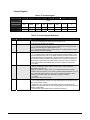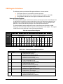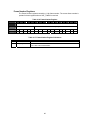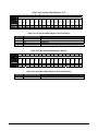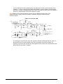
1
DSTni-EX User Guide
Section Five
Part Number 900-335
Revision A 3/04
Copyright & Trademark
© 2003 Lantronix, Inc. All rights reserved.
Lantronix and the Lantronix logo, and combinations thereof are registered trademarks of
Lantronix, Inc. DSTni is a registered trademark of Lantronix, Inc. Ethernet is a registered
trademark of Xerox Corporation. All other product names, company names, logos or other
designations mentioned herein are trademarks of their respective owners.
Am186 is a trademark of Advanced Micro Devices, Inc.
Ethernet is a registered trademark of Xerox Corporation.
SPI is a trademark of Motorola, Inc.
No part of this guide may be reproduced or transmitted in any form for any purpose other than
the purchaser's personal use, without the express written permission of Lantronix, Inc.
Lantronix
15353 Barranca Parkway
Irvine, CA 92618, USA
Phone: 949-453-3990
Fax:
949-453-3995
Technical Support
Phone: 630-245-1445
Fax:
630-245-1717
Master Distributor
Grid Connect
1841 Centre Point Circle, Suite 143
Naperville, IL 60563
Phone: 630-245-1445
www.gridconnect.com
Am186 is a trademark of Advanced Micro Devices, Inc.
Ethernet is a registered trademark of Xerox Corporation.
SPI is a trademark of Motorola, Inc.
REV
A
Changes
Reformat. Add changes from Design
Spec. 1.1
i
Released Date
3-24-04
Warranty
Lantronix warrants each Lantronix product to be free from defects in material and workmanship
for a period specified on the product warranty registration card after the date of shipment.
During this period, if a customer is unable to resolve a product problem with Lantronix Technical
Support, a Return Material Authorization (RMA) will be issued. Following receipt of an RMA
number, the customer shall return the product to Lantronix, freight prepaid. Upon verification of
warranty, Lantronix will -- at its option -- repair or replace the product and return it to the
customer freight prepaid. If the product is not under warranty, the customer may have Lantronix
repair the unit on a fee basis or return it. No services are handled at the customer's site under
this warranty. This warranty is voided if the customer uses the product in an unauthorized or
improper way, or in an environment for which it was not designed.
Lantronix warrants the media containing its software product to be free from defects and
warrants that the software will operate substantially according to Lantronix specifications for a
period of 60 DAYS after the date of shipment. The customer will ship defective media to
Lantronix. Lantronix will ship the replacement media to the customer.
*
*
*
*
In no event will Lantronix be responsible to the user in contract, in tort (including negligence),
strict liability or otherwise for any special, indirect, incidental or consequential damage or loss of
equipment, plant or power system, cost of capital, loss of profits or revenues, cost of
replacement power, additional expenses in the use of existing software, hardware, equipment or
facilities, or claims against the user by its employees or customers resulting from the use of the
information, recommendations, descriptions and safety notations supplied by Lantronix.
Lantronix liability is limited (at its election) to:
refund of buyer's purchase price for such affected products (without interest)
repair or replacement of such products, provided that the buyer follows the above procedures.
There are no understandings, agreements, representations or warranties, express or implied,
including warranties of merchantability or fitness for a particular purpose, other than those
specifically set out above or by any existing contract between the parties. Any such contract
states the entire obligation of Lantronix. The contents of this document shall not become part of
or modify any prior or existing agreement, commitment or relationship.
For details on the Lantronix warranty replacement policy, go to our web site at
http://www.lantronix.com/support/warranty/index.html
ii
Contents
Copyright & Trademark ________________________________________________________i
Warranty___________________________________________________________________ ii
Contents___________________________________________________________________ iii
List of Tables _______________________________________________________________ iv
List of Figures_______________________________________________________________ vi
1: About This User Guide _________________________________________ 1
Intended Audience ___________________________________________________________ 2
Conventions ________________________________________________________________ 2
Navigating Online____________________________________________________________ 2
Organization________________________________________________________________ 3
2: SPI Controller ________________________________________________ 4
Theory of Operation __________________________________________________________ 4
SPI Background___________________________________________________________ 4
DSTni SPI Controller _______________________________________________________ 4
SPI Controller Register Summary _______________________________________________ 5
SPI Controller Register Definitions ______________________________________________ 6
SPI_DATA Register ________________________________________________________ 6
CTL Register _____________________________________________________________ 7
SPI_STAT Register ________________________________________________________ 8
SPI_SSEL Register ________________________________________________________ 9
DVD_CNTR_LO Register __________________________________________________ 10
DVD_CNTR_HI __________________________________________________________ 10
3: I2C Controller ________________________________________________ 11
Features __________________________________________________________________ 11
Block Diagram _____________________________________________________________ 12
Theory of Operation _________________________________________________________ 12
I2C Background __________________________________________________________ 12
I2C Controller ____________________________________________________________ 13
Operating Modes _________________________________________________________ 13
Bus Clock Considerations __________________________________________________ 21
Programmer’s Reference _____________________________________________________ 22
I2C Controller Register Summary_______________________________________________ 22
I2C Controller Register Definitions ______________________________________________ 23
Slave Address Register ____________________________________________________ 23
Data Register____________________________________________________________ 24
Control Register__________________________________________________________ 25
Status Register __________________________________________________________ 26
Clock Control Register_____________________________________________________ 28
Extended Slave Address Register ____________________________________________ 29
Software Reset Register ___________________________________________________ 29
4: USB Controller ______________________________________________ 30
Features __________________________________________________________________ 30
Theory of Operation _________________________________________________________ 31
USB Background _________________________________________________________ 31
USB Interrupt ____________________________________________________________ 31
USB Core_______________________________________________________________ 31
USB Hardware/Software Interface ___________________________________________ 32
USB Transaction _________________________________________________________ 37
USB Register Summary______________________________________________________ 38
USB Register Definitions _____________________________________________________ 39
Interrupt Status Register ___________________________________________________ 39
Error Register ___________________________________________________________ 41
Status Register __________________________________________________________ 43
Address Register _________________________________________________________ 45
Frame Number Registers __________________________________________________ 46
Token Register __________________________________________________________ 47
Endpoint Control Registers _________________________________________________ 49
iii
Host Mode Operation ________________________________________________________ 50
Sample Host Mode Operations ________________________________________________ 51
USB Pull-up/Pull-down Resistors_______________________________________________ 53
USB Interface Signals _______________________________________________________ 54
5: CAN Controllers _____________________________________________ 55
CANBUS Background _______________________________________________________ 56
Data Exchanges and Communication _________________________________________ 56
Arbitration and Error Checking ______________________________________________ 56
CANBUS Speed and Length ________________________________________________ 57
Features __________________________________________________________________ 57
Theory of Operation _________________________________________________________ 58
CAN Register Summaries ____________________________________________________ 58
Register Summary ________________________________________________________ 58
Detailed CAN Register Map_________________________________________________ 60
CAN Register Definitions _____________________________________________________ 63
TX Message Registers ____________________________________________________ 63
Tx Message Registers _____________________________________________________ 64
RX Message Registers ____________________________________________________ 66
Rx Message Registers_____________________________________________________ 67
Error Count and Status Registers ____________________________________________ 70
Interrupt Flags ___________________________________________________________ 72
Interrupt Enable Registers __________________________________________________ 73
CAN Operating Mode _____________________________________________________ 74
CAN Configuration Registers _______________________________________________ 75
Acceptance Filter and Acceptance Code Mask__________________________________ 78
CANbus Analysis _________________________________________________________ 81
CAN Bus Interface __________________________________________________________ 84
Interface Connections _____________________________________________________ 84
List of Tables
Table 2-1. SPI Controller Register Summary .............................................................................. 5
Table 2-2. SPI_DATA Register ................................................................................................... 6
Table 2-3. SPI_DATA Register Definitions.................................................................................. 6
Table 2-4. CTL Register .............................................................................................................. 7
Table 2-5. CTL Register Definitions ............................................................................................ 7
Table 2-6. SPI_STAT Register.................................................................................................... 8
Table 2-7. SPI_STAT Register Definitions .................................................................................. 8
Table 2-8. SPI_SSEL Register.................................................................................................... 9
Table 2-9. SPI_SSEL Register Definitions .................................................................................. 9
Table 2-10. BCNT Bit Settings .................................................................................................... 9
Table 2-11. DVD_CNTR_LO Register ...................................................................................... 10
Table 2-12. DVD_CNTR_LO Register Definitions..................................................................... 10
Table 2-13. DVD_CNTR_HI Register........................................................................................ 10
Table 2-14. DVD_CNTR_HI Register Definitions ...................................................................... 10
Table 3-1. Master Transmit Status Codes................................................................................. 14
Table 3-2. Codes After Servicing Interrupts (Master Transmit) ................................................. 15
Table 3-3. Status Codes After Each Data Byte Transmits ........................................................ 16
Table 3-4. Master Receive Status Codes.................................................................................. 17
Table 3-5. Codes After Servicing Interrupt (Master Receive) .................................................... 18
Table 3-6. Codes After Receiving Each Data Byte.................................................................... 19
Table 3-7. I2C Controller Register Summary ............................................................................. 22
Table 3-8. Slave Address Register............................................................................................ 23
Table 3-9. Address Register Definitions.................................................................................... 23
Table 3-10. Data Register ......................................................................................................... 24
Table 3-11. Data Register Definitions ....................................................................................... 24
Table 3-12. Control Register ..................................................................................................... 25
Table 3-13. Control Register Definitions ................................................................................... 25
Table 3-14. Status Register ...................................................................................................... 26
Table 3-15. Status Register Definitions..................................................................................... 27
Table 3-16. Status Codes ......................................................................................................... 27
iv
Table 3-17. Clock Control Register ........................................................................................... 28
Table 3-18. Clock Control Register Definitions.......................................................................... 28
Table 3-19. Extended Slave Address Register ......................................................................... 29
Table 3-20. Extended Slave Address Register Definitions........................................................ 29
Table 3-21. Software Reset Register ........................................................................................ 29
Table 3-22. Software Reset Register Definitions....................................................................... 29
Table 4-1. USB Data Direction .................................................................................................. 34
Table 4-2. 16-Bit USB Address ................................................................................................. 34
Table 4-3. 16-Bit USB Address Definitions ............................................................................... 34
Table 4-4. BDT Data Used by USB Controller and Microprocessor .......................................... 35
Table 4-5. USB Buffer Descriptor Format ................................................................................. 35
Table 4-6. USB Buffer Descriptor Format Definitions................................................................ 36
Table 4-7. USB Register Summary ........................................................................................... 38
Table 4-8. Interrupt Status Register .......................................................................................... 39
Table 4-9. 16- Interrupt Status Register Definitions .................................................................. 39
Table 4-10. Error Interrupt Status Register ............................................................................... 41
Table 4-11. 16- Error Interrupt Status Register Definitions ....................................................... 41
Table 4-12. Status Register ...................................................................................................... 43
Table 4-13. Status Register Definitions..................................................................................... 43
Table 4-14. Address Register ................................................................................................... 45
Table 4-15. 16- Address Register Definitions............................................................................ 45
Table 4-16. Frame Number Register......................................................................................... 46
Table 4-17. Frame Number Register Definitions ....................................................................... 46
Table 4-18. Token Register....................................................................................................... 48
Table 4-19. Token Register Definitions ..................................................................................... 48
Table 4-20. Valid PID Tokens ................................................................................................... 48
Table 4-21. Endpoint Control Registers .................................................................................... 49
Table 4-22. Endpoint Control Register Definitions .................................................................... 49
Table 4-23. Endpoint Control Register Definitions .................................................................... 50
Table 5-1. Bit Rates for Different Cable Lengths....................................................................... 57
Table 5-2. CAN I/O Address ..................................................................................................... 58
Table 5-3. CAN Channel Register Summary ............................................................................ 58
Table 5-4. Detailed CAN Register Map ..................................................................................... 60
Table 5-5. TxMessage_0:ID28 .................................................................................................. 64
Table 5-6. TxMessage_0:ID12 .................................................................................................. 64
Table 5-7. TxMessage_0:Data 55 ............................................................................................. 64
Table 5-8. TxMessage_0:Data 39 ............................................................................................. 64
Table 5-9. TxMessage_0:Data 23 ............................................................................................. 64
Table 5-10. TxMessage_0:Data 7 ............................................................................................. 64
Table 5-11. TxMessage_0:RTR ................................................................................................ 64
Table 5-12. TxMessage_0:Ctrl Flags ........................................................................................ 65
Table 5-13. TxMessage_0 Register Definitions......................................................................... 65
Table 5-14. RxMessage:ID28 ................................................................................................... 67
Table 5-15. Rx Message: ID28 Register Definitions.................................................................. 67
Table 5-16. RxMessage:ID12 ................................................................................................... 67
Table 5-17. Rx Message: ID12 Register Definitions.................................................................. 67
Table 5-18. Rx Message: Data 55............................................................................................. 67
Table 5-19. Rx Message: Data 55 Register Definitions............................................................. 67
Table 5-20. Rx Message: Data 39............................................................................................. 68
Table 5-21. Rx Message: Data 39 Register Definitions............................................................. 68
Table 5-22. Rx Message: Data 23............................................................................................. 68
Table 5-23. Rx Message: Data 23 Register Definitions............................................................. 68
Table 5-24. Rx Message: Data 7............................................................................................... 68
Table 5-25. Rx Message: Data 7 Register Definitions............................................................... 68
Table 5-26. RxMessage: RTR................................................................................................... 69
Table 5-27. Rx Message: RTR Register Definitions.................................................................. 69
Table 5-28. Rx Message: Msg Flags......................................................................................... 69
Table 5-29. Rx Message: Msg Flags Register Definitions......................................................... 69
Table 5-30. Tx/Rx Error Count .................................................................................................. 70
Table 5-31. Tx\Rx Error Count Register Definitions .................................................................. 70
Table 5-32. Error Status............................................................................................................ 70
Table 5-33. Error Status Register Definitions ............................................................................ 70
v
Table 5-34. Tx/Rx Message Level Register .............................................................................. 71
Table 5-35. Tx/Rx Message Level Register Definitions............................................................. 71
Table 5-36. Interrupt Flags ........................................................................................................ 72
Table 5-37. Interrupt Flag Definitions ........................................................................................ 72
Table 5-38. Interrupt Enable Registers ..................................................................................... 73
Table 5-39. Interrupt Enable Register Definitions...................................................................... 73
Table 5-40. Interrupt Enable Registers ..................................................................................... 74
Table 5-41. Interrupt Enable Register Definitions...................................................................... 74
Table 5-42. Bit Rate Divisor Register ........................................................................................ 75
Table 5-43. Bit Rate Divisor Register Definitions ...................................................................... 75
Table 5-44. Configuration Register ........................................................................................... 76
Table 5-45. Configuration Register Definitions.......................................................................... 76
Table 5-46. Acceptance Filter Enable Register ......................................................................... 78
Table 5-47. Acceptance Filter Enable Register Definitions ....................................................... 78
Table 5-48. Acceptance Mask 0 Register ................................................................................. 78
Table 5-49. Acceptance Mask 0 Register Definitions................................................................ 78
Table 5-50. Acceptance Mask Register: ID 12 .......................................................................... 79
Table 5-51. Acceptance Mask Register: ID12 Definitions ......................................................... 79
Table 5-52. Acceptance Mask Register: Data 55 ...................................................................... 79
Table 5-53. Acceptance Mask Register: Data 55 Definitions .................................................... 79
Table 5-54. Acceptance Code Register .................................................................................... 80
Table 5-55. Acceptance Code Register Definitions................................................................... 80
Table 5-56. Acceptance Mask Register: ID12 ........................................................................... 80
Table 5-57. Acceptance Mask Register: ID12 Definitions ......................................................... 80
Table 5-58. Acceptance Mask Register: Data 55 ...................................................................... 80
Table 5-59. Acceptance Mask Register: Data 55 Definitions .................................................... 80
Table 5-60. Arbitration Lost Capture Register ........................................................................... 81
Table 5-61. Arbitration Lost Capture Register Definitions ......................................................... 81
Table 5-62. Error Capture Register ........................................................................................... 82
Table 5-63. Error Capture Register Definitions ......................................................................... 82
Table 5-64. Frame Reference Register..................................................................................... 83
Table 5-65. Error Capture Register Definitions ......................................................................... 83
List of Figures
Figure 3-1. DSTni I2C Controller Block Diagram ....................................................................... 12
Figure 4-1. Buffer Descriptor Table ........................................................................................... 33
Figure 4-2. USB Token Transaction.......................................................................................... 37
Figure 3. Enable Host Mode and Configure a Target Device .................................................... 51
Figure 4. Full-Speed Bulk Data Transfers to a Target Device................................................... 52
Figure 4-5. Pull-up/Pull-down USB............................................................................................ 53
Figure 5-1. TX Message Routing .............................................................................................. 63
Figure 5-2. RX Message Routing .............................................................................................. 66
Figure 5-3. CAN Operating Mode.............................................................................................. 75
Figure 5-4. Bit Time, Time Quanta, and Sample Point Relationships ....................................... 77
Figure 5-5. CAN Bus Interface .................................................................................................. 84
Figure 5-6. CAN Connector....................................................................................................... 84
Figure 5-7. Power for CAN ........................................................................................................ 85
Figure 5-8. CAN Transceiver and Isolation Circuits .................................................................. 86
vi
1: About This User Guide
This User Guide describes the technical features and programming interfaces of the Lantronix
DSTni-EX chip (hereafter referred to as “DSTni”).
DSTni is an Application Specific Integrated Circuit (ASIC)-based single-chip solution (SCS) that
integrates the leading-edge functionalities needed to develop low-cost, high-performance device
server products. On a single chip, the DSTni integrates an x186 microprocessor, 16K-byte
ROM, 256K-byte SRAM, programmable input/output (I/O), and serial, Ethernet, and Universal
Serial Bus (USB) connectivity — key ingredients for device- server solutions. Although DSTni
embeds multiple functions onto a single chip, it can be easily customized, based on the
comprehensive feature set designed into the chip.
Providing a complete device server solution on a single chip enables system designers to build
affordable, full-function solutions that provide the highest level of performance in both
processing power and peripheral systems, while reducing the number of total system
components. The advantages gained from this synergy include:
Simplifying system design and increased reliability.
Minimizing marketing and administration costs by eliminating the need to source
products from multiple vendors.
Eliminating the compatibility and reliability problems that occur when combining
separate subsystems.
Dramatically reducing implementation costs.
Increasing performance and functionality, while maintaining quality and cost
effectiveness.
Streamlining development by reducing programming effort and debugging time.
Enabling solution providers to bring their products to market faster.
These advantages make DSTni the ideal solution for designs requiring x86 compatibility;
increased performance; serial, programmable I/O, Ethernet, and USB communications; and a
glueless bus interface.
1
Intended Audience
This User Guide is intended for use by hardware and software engineers, programmers, and
designers who understand the basic operating principles of microprocessors and their systems
and are considering designing systems that utilize DSTni.
Conventions
This User Guide uses the following conventions to alert you to information of special interest.
The symbols # and n are used throughout this Guide to denote active LOW signals.
Notes: Notes are information requiring attention.
Navigating Online
The electronic Portable Document Format (PDF) version of this User Guide contains hyperlinks.
Clicking one of these hyper links moves you to that location in this User Guide. The PDF file
was created with Bookmarks and active links for the Table of Contents, Tables, Figures and
cross-references.
2
Organization
This User Guide contains information essential for system architects and design engineers. The
information in this User Guide is organized into the following chapters and appendixes.
Section 1: Introduction
Describes the DSTni architecture, design benefits, theory of operations, ball
assignments, packaging, and electrical specifications. This chapter includes a
DSTni block diagram.
Section 2: Microprocessor
Describes the DSTni microprocessor and its control registers.
Section 2: SDRAM
Describes the DSTni SDRAM and the registers associated with it.
Section 3: Serial Ports
Describes the DSTni serial ports and the registers associated with them.
Section 3: Programmable Input/Output
Describes DSTni’s Programmable Input/ Output (PIO) functions and the
registers associated with them.
Section 3: Timers
Describes the DSTni timers.
Section 4: Ethernet Controllers
Describes the DSTni Ethernet controllers.
Section 4: Ethernet PHY
Describes the DSTni Ethernet physical layer core.
Section 5: SPI Controller
Describes the DSTni Serial Peripheral Interface (SPI) controller.
Section 5: I2C Controller
Describes the DSTni I2C controller.
Section 5: USB Controller
Describes the DSTni USB controller.
Section 5: CAN Controllers
Describes the DSTni Controller Area Network (CAN) bus controllers.
Section 6: Interrupt Controller
Describes the DSTni interrupt controller.
Section 6: Miscellaneous Registers
Describes DSTni registers not covered in other chapters of this Guide.
Section 6: Debugging In-circuit Emulator (Delce)
Section 6: Packaging and Electrical
Describes DSTni’s packaging and electrical characteristics.
Section 6: Applications
Describes DSTni’s packaging and electrical characteristics.
Section 6: Instruction Clocks
Describes the DSTni instruction clocks.
Section 6: DSTni Sample Code
Section 6: Baud Rate Calculations
Provides baud rate calculation tables.
3
2: SPI Controller
This chapter describes the DSTni Serial Peripheral Interface (SPI) controller. Topics include:
Theory of Operation on page 4
SPI Controller Register Summary on page 5
SPI Controller Register Definitions on page 6
Theory of Operation
SPI Background
SPI is a high-speed synchronous serial input/output (I/O) port that allows a serial bit stream of
programmed length (one to eight bits) to be shifted into and out of the device at a
programmable bit-transfer rate.
SPI is an industry-standard communications interface that does not have specifications or a
standards organizing group. As a result, there are no licensing requirements. Because of its
simplicity, SPI is commonly used in embedded systems. Many semiconductor manufacturers
sell a variety of sensor, conversion, and control devices that use SPI.
DSTni SPI Controller
The DSTni SPI controller is located at base I/O address B800h. It shares an interrupt with the
I2C controller and connects to interrupt 2. The SPI controller is enabled using the DSTni
Configuration register. If set to 1, the SPI controller is enabled on serial port 3. This bit can
reset to 1 with an external pull-up resistor. Normally it resets to 0 on reset or power-up.
The SPI bus is a 3-wire bus serial bus that links a serial shift register between a master device
and a slave device. This design supports both master and slave operations. Typically, master
and slave devices have an 8-bit shift register, for a combined register of 16 bits. During an SPI
transfer, the master and slave shift registers by eight bits and exchange their 8-bit register
values, starting with the most-significant bit.
The SPI interface is software configurable. The clock polarity, clock phase, SLVSEL polarity,
clock frequency in master mode, and number of bits to be transferred are all software
programmable. SPI supports multiple slaves on a single 3-wire bus by using separate Slave
Select signals to enable the desired slave. Multiple masters are also fully supported and some
support is provided for detecting collisions when multiple masters attempt to transfer at the
same time.
A Wired-OR mode is provided which allows multiple masters to collide on the bus without risk of
damage. In this mode, an external pull-up resistor is required on the Master Out Slave In
(MOSI) ) and Master In Slave Out (MISO) pins. The wired-OR mode also allows the SPI bus to
operate as a 2-wire bus by connecting the MOSI and MISO pins to form a single bi-directional
data pin. Generally, pull-ups are recommended on all of the external SPI signals to ensure they
are held in a valid state, even when the SPI interface is disabled. For some device connections,
the ALT mode bit will swap the TX and RX pins.
The SPI controller has an enhanced mode called AUTODRV. This mode is valid in master
mode. In this mode, the SLVSEL pin is driven active when data is written to the data register.
After the last bit of data is shifted out, the SLVSEL goes inactive and an interrupt is generated.
The INVCS bit can generate either a positive or negative true SLVSEL pin.
4
When operating as a slave, the SPI clock signal (SCLK) must be slower than 1/8th of the CPU
clock (1/16th is recommended).
Note: The SPI is fully synchronous to the CLK signal. As a result, SCLK is sampled and then
operated on. This results in a delay of 3 to 4 clocks, which may violate the SPI specification if
SCLK is faster than 1/8th of the CPU clock. In master mode, the SPI operates exactly on the
proper edges, since the SPI controller is generating SCLK.
The SPI controller uses a 16-bit counter that is continually reloaded from DVD_CNTR_HI and
DVD_CNTR_LO. The counter divides the CPU clock by this divider and uses the result to
generate SCLK.
The SPI interface includes the internal interrupt connection, SPI interrupt.
In SPI master mode, an SPI interrupt occurs when the Transmit Holding register is
empty.
In SPI slave mode, an SPI interrupt occurs when the SLVSEL pin transitions from active
to inactive.
A familiar Interrupt Control register is provided for the SPI interrupt. The interrupt has a two
CPU clock delay from SLVSEL in slave mode because of synchronization registers.
SPI Controller Register Summary
Table 2-1. SPI Controller Register Summary
Hex Address
B800
B802
B804
B806
B808
B80A
Mnemonic
Register Description
SPI_DATA
CTL
SPI_STAT
SPI_SSEL
DVD_CNTR_LO
DVD_CNTR_HI
Data register
Control register
Status register
Slave Select Bit Count register
DVD Counter Low Byte register
DVD Counter High Byte register
5
Page
6
7
8
9
10
10
SPI Controller Register Definitions
SPI_DATA Register
SPI_DATA is the SPI Controller Data register.
Table 2-2. SPI_DATA Register
BIT
OFFSET
15
14
13
12
10
9
8
7
6
5
4
3
2
1
0
B800
///
FIELD
RESET
RW
11
0
0
0
0
0
0
0
0
0
0
0
RW
RW
R
W
RW
RW
RW
RW
RW
RW
RW
RW
DATA[7:0]
0
0
RW
RW
0
0
0
RW
RW
RW
Table 2-3. SPI_DATA Register Definitions
Bits
15:8
7:0
Field Name
///
DATA[7:0]
Description
Reserved
Always returns zero.
Data
The location where the CPU reads data from or writes data for the SPI interface.
6
CTL Register
CTL is the SPI Controller Control register.
Table 2-4. CTL Register
15
14
13
12
11
10
9
8
7
4
3
2
1
0
ALT
MSTN
WOR
CKPOL
PHASE
///
RW
5
INVCS
IRQENB
FIELD
RESET
6
B802
AUTODRV
BIT
OFFSET
0
0
0
0
0
0
0
0
0
0
0
0
0
0
0
0
RW
RW
RW
RW
R
W
RW
RW
RW
RW
RW
RW
RW
RW
RW
RW
RW
Table 2-5. CTL Register Definitions
Bits
Field Name
15:8
7
///
IRQENB
6
AUTODRV
5
INVCS
4
PHASE
3
CKPOL
2
WOR
1
MSTN
0
ALT
Description
Reserved
Always returns zero.
Interrupt Request Enable
1 = enable the SPI to generate interrupts.
0 = disable the SPI from generating interrupts (default).
Autodrv
1 = enabled. Autodrv generates the sequence of selecting the serial device (CS)
and transferring data to it and then deselecting the device with no CPU
interaction. The transfer is started by writing to the data register.
0 = disabled (default).
Invert Chip Select
1 = inverted CS.
0 = normal (default).
Phase Select
Selects the operating mode for the SPI interface. The two modes select where
the opposite edge D-Flip-Flop is placed.
1 = the negative edge flop is inserted into the shift_out path to hold the data for an
extra ½ clock.
0 = a negative edge flop is inserted into the shift_in path (default).
Clock Polarity
Controls the polarity of the SCLK (SPI clock).
1 = SCLK idles HIGH.
0 = SCLK idles LOW (default).
Wire-O
HIGH = WOR bit configures the SPI bus to operate as an Open-Drain. This
prevents SPI bus conflicts when there are multiple bus masters.
LOW = WOR bit does not configure the SPI bus to operate as an Open-Drain.
Master Enable
Selects master or slave mode for the SPI interface.
1 = master mode.
0 = slave mode (default).
Alternate I/O Pinouts
Enable alternate I/O pinouts.
1 = alternate I/O.
0 = normal (default).
7
SPI_STAT Register
To clear a bit in the SPI_STAT register, write a 1 to that bit.
14
13
12
11
10
9
8
7
4
3
2
///
COL
IRQ
///
RW
5
1
0
B804
FIELD
RESET
6
SLVSEL
15
OVERRUN
BIT
OFFSET
TXRUN
Table 2-6. SPI_STAT Register
0
0
0
0
0
0
0
0
0
0
0
0
0
0
0
0
RW
RW
RW
RW
RW
RW
RW
RW
RW
RW
RW
RW
RW
RW
R
R
Table 2-7. SPI_STAT Register Definitions
Bits
Field Name
15:8
///
7
IRQ
6
OVERRUN
5
COL
4:2
1
TXRUN
0
SLVSEL
///
Description
Reserved
Always returns zero.
Interrupt Request
1 = indicates the end of a master mode transfer, or that SLVSEL_N input has
gone HIGH on a slave transfer.
0 = indicates no end of a master mode transfer, or that SLVSEL_N input has not
gone HIGH on a slave transfer (default).
It takes two CPU clocks after SLVSEL_n changes to see the interrupt.
Overrun
1 = SPIDAT register is written to while an SPI transfer is in progress or
SLVSEL_N goes active in master mode.
0 = SPIDAT register has not been written to or SLVSEL_N has not gone active in
master mode (default).
Collision
1 = a master mode collision has occurred between multiple SPI masters (SLVSEL
is active while MSTEN=1).
0 = a master mode collision has not occurred (default).
Reserved
Transmitter Running
1 = master mode operation underway.
0 = idle (default).
SLVSEL Pin
Corresponds to the SLVSEL (MSCS*) pin on SPI core (pin is normally inverted at
the I/O pin).
8
SPI_SSEL Register
SPI_SSEL is the Slave Select Bit Count register.
Table 2-8. SPI_SSEL Register
BIT
OFFSET
15
14
13
12
11
10
9
8
7
6
5
4
3
2
1
///
RW
BCNT[2:0]
SELECTO
FIELD
RESET
0
B806
///
0
0
0
0
0
0
0
0
0
0
0
0
0
0
0
0
RW
RW
RW
RW
RW
RW
RW
RW
RW
RW
RW
RW
RW
RW
RW
RW
Table 2-9. SPI_SSEL Register Definitions
Bits
15:8
7:6
5:1
0
Field Name
Description
///
Reserved
Always returns zero.
Bit Shift Count
Controls the number of bits shifted between the master and slave device during a
transfer, when this device is the master. See Table 2-10.
Reserved
Always returns zero.
SelectO Signal
This bit is the select output for master mode.
1 = this bit drives the SLVSEL pin active.
0 = this bit inactivates SLVSEL (default).
This bit is not used with Autodrv. If using Autodrv, leave this bit set to 0. The
INVCS is used to invert the SLVSEL for active LOW devices.
BCNT[2:0]
///
SELECTO
Table 2-10. BCNT Bit Settings
Bit [2]
0
0
0
0
1
1
1
1
BCNT[2:0]
Bit [1]
Number of Bits Shifted
Bit [0]
0
0
1
1
0
0
1
1
0
1
0
1
0
1
0
1
9
8 (default)
1
2
3
4
5
6
7
DVD_CNTR_LO Register
DVD_CNTR_LO is the DVD Counter Low Byte register.
Table 2-11. DVD_CNTR_LO Register
BIT
OFFSET
15
14
13
12
11
10
9
8
7
6
5
4
///
FIELD
RESET
RW
3
2
1
0
B808
DVDCNT[7:0]
0
0
0
0
0
0
0
0
0
0
0
0
0
0
RW
RW
RW
RW
RW
RW
RW
RW
RW
RW
RW
RW
RW
RW
0
0
RW
RW
Table 2-12. DVD_CNTR_LO Register Definitions
Bits
Field Name
15:8
7:0
Description
///
Reserved
Always returns zero.
Divisor Select
Selects the SPI clock rate during master mode. DVD_CNTR_HI and this byte
generate a 16-bit divisor that generates the SPI clock.
DVDCNT[7:0]
DVD_CNTR_HI
DVD_CNTR_HI is the DVD Counter High Byte register.
Table 2-13. DVD_CNTR_HI Register
BIT
OFFSET
FIELD
RESET
RW
15
14
13
12
11
10
9
8
7
6
5
4
3
2
1
0
B80A
///
DVDCNT[15:8]
0
0
0
0
0
0
0
0
0
0
0
0
0
0
RW
RW
RW
RW
RW
RW
RW
RW
RW
RW
RW
RW
RW
RW
0
0
RW
RW
Table 2-14. DVD_CNTR_HI Register Definitions
Bits
15:8
7:0
Field Name
///
DVDCNT[15:8]
Description
Reserved
Always returns zero.
Divisor Select
Selects the SPI clock rate during master mode. DVD_CNTR_LO and this byte
generate a 16-bit divisor that generates the SPI clock.
10
3: I2C Controller
This chapter describes the DSTni I2C controller. Topics include:
Features on page 11
Block Diagram on page 12
Theory of Operation on page 12
Programmer’s Reference on page 22
I2C Controller Register Summary on page 22
I2C Controller Register Definitions on page 23
Features
Master or slave operation
Multmaster operation
Software selectable acknowledge bit
Arbitration-lost interrupt with automatic mode switching from master to slave
Calling address identification interrupt with automatic mode switching from master to
slave
START and STOP signal generation/detection
Repeated START signal generation
Acknowledge bit generation/detection
Bus busy detection
100 KHz to 400 KHz operation
11
Block Diagram
Figure 3-1 shows a block diagram of the DSTni I2C controller.
Figure 3-1. DSTni I2C Controller Block Diagram
Theory of Operation
I2C Background
2
The I C bus is a popular serial, two-wire interface used in many systems because of its low
overhead. Capable of 100 KHz operation, each device connected to the bus is software
addressable by a unique address, with a simple master/slave protocol.
2
The I C bus consists of two wires, serial data (SDA), and a serial clock (SCL), which carry
information between the devices connected to the bus. This two-wire interface minimizes
interconnections, so integrated circuits have fewer pins, and the number of traces required on
printed circuit boards is reduced.
The number of devices connected to the same bus is limited only by a maximum bus
capacitance of 400 pF. Both the SDA and SCL lines are bidirectional, connected to a positive
supply voltage via a pull-up resistor. When the bus is free, both lines are HIGH. The output
stages of devices connected to the bus must have an open-drain or open-collector to perform
the wired-AND function.
Each device on the bus has a unique address and can operate as either a transmitter or
receiver. In addition, devices can also be configured as masters or slaves.
A master is the device that initiates a data transfer on the bus and generates the clock
signals to permit that transfer.
Any other device that is being addressed is considered a slave.
2
The I C protocol defines an arbitration procedure to ensure that if more than one master
simultaneously tries to control the bus, only one is allowed to do so and the message is not
2
corrupted. The arbitration and clock synchronization procedures defined in the I C specification
2
are supported by the DSTni I C controller.
12
I2C Controller
The I2C controller base address is D000h and shares INT2 with the SPI controller. The I2C bus
interface requires two bi-directional buffers with open collector (or open drain) outputs and
Schmitt inputs.
Operating Modes
The following sections describe the possible I2C operating modes:
Master Transmit Mode, page 13
Master Receive Mode, page 16
Slave Transmit Mode, page 19
Slave Receive Mode, page 20
Master Transmit Mode
In master transmit mode, the I2C controller transmits a number of bytes to a slave receiver.
To enter the master transmit mode, set the STA bit to one. The following actions occur:
1. The DATA register loads either a 7-bit slave address or the first part of a 10-bit slave
address, with the least-significant bits cleared to zero, to specify transmit mode.
2. The M I2C tests the I2C bus and sends a START condition when the bus is free.
3. The IFLG bit is set and the status code in the Status register becomes 08h.
4. The IFLG bit clears to zero to prompt the transfer to continue.
5. After the 7-bit slave address (or the first part of a 10-bit address) and the write bit are sent,
the IFLG is set again.
During this sequence, a number of status codes are possible in the Status register (see Table
3-1).
Note: In 10-bit addressing, after the first part of a 10-bit address and the write bit transmit
successfully, the status code is 18h or 20h.
13
Table 3-1. Master Transmit Status Codes
Code
I2C State
Microprocessor Response
18h
Addr + W transmitted,
ACK received
7-bit address:
Write byte to DATA, clear IFLG
Next I2C Action
Transmit data byte, receive
ACK
OR
Set STA, clear IFLG
Transmit repeated START
OR
Set STP, clear IFLG
Transmit STOP
OR
Set STA & STP, clear IFLG
20h
38h
Addr + W transmitted,
ACK not received
Arbitration lost
Transmit STOP, then START
10-bit address:
Write extended address byte to
DATA, clear IFLG
Same as code 18h
Same as code 18h
Clear IFLG
Return to idle
Transmit extended address byte
OR
68h
78h
B0h
Arbitration lost,
SLA + W received,
ACK transmitted
Set STA, clearIFLG
Clear IFLG, AAK=0
Transmit START when bus is free
Receive data byte, transmit not ACK
OR
Clear IFLG, AAK=1
Arbitration lost,
Same as code 68h
general call addr
received, ACK
transmitted
Arbitration lost, SLA + R Write byte to DATA, clear IFLG,
received, ACK
AAK=0
transmitted
OR
Receive data byte, transmit ACK
Same as code 68h
Write byte to DATA, clear IFLG,
AAK=1
Transmit data byte, receive ACK
14
Transmit last byte, receive ACK
Servicing the Interrupt
After servicing this interrupt, and transmitting the second part of the address, the Status register
contains one of the codes in Table 3-2.
Note: If a repeated START condition transmits, the status code is 10h instead of 08h.
Table 3-2. Codes After Servicing Interrupts (Master Transmit)
2
Code
I C State
Microprocessor Response
Next I2C Action
38h
Arbitration lost
Clear IFLG
Return to idle
OR
68h
B0h
Arbitration lost,
SLA + W received,
ACK transmitted
Arbitration lost,
SLA + R received,
ACK transmitted
Set STA, clear IFLG
Clear IFLG, AAK=0
Transmit START when bus free
Receive data byte, transmit not ACK
OR
Clear IFLG, AAK=1
Write byte to DATA, Clear IFLG,
AAK=0
Receive data byte, transmit ACK
Transmit data byte, receive ACK
OR
D0h
Second Address byte +
W, transmitted ACK
received
Write byte to DATA, Clear IFLG,
AAK=1
Write byte to DATA, clear IFLG
Transmit data byte, receive ACK
Transmit data byte, receive ACK
OR
Set STA, clear IFLG
Transmit repeated START
OR
Set STP, clear IFLG
Transmit STOP
OR
D8h
Second Address byte +
W, transmitted ACK
received
Set STA & STP, clear IFLG
Same as code D0h
15
Transmit STOP, then START
Same as code D0h
Transmitting Each Data Byte
After each data byte transmits, the IFLG is set, and one of the three status codes in Table 3-3 is
in the Status register.
Table 3-3. Status Codes After Each Data Byte Transmits
2
Code
I C State
Microprocessor Response
Next I2C Action
28h
Data byte transmitted,
ACK received
Write byte to DAT, clear IFLG
Transmit data byte, receive ACK
OR
Set STA, clear IFLG
Transmit repeated START
OR
Set STP, clear IFLG
Transmit STOP
OR
30h
38h
Data byte transmitted,
ACK not received
Arbitration lost
Set STA and STP, clear IFLG
Same as code 28h
Transmit START then STOP
Same as code 28h
Clear IFLG
Return to idle
OR
Set STA, clear IFLG
Transmit START when bus free
All Bytes Transmit Completely
When all bytes transmit completely, set the STP bit by writing a 1 to this bit in the Control
register. The I2C controller:
Transmits a STOP condition
Clears the STP bit
Returns to the idle state
Master Receive Mode
In master receive mode, the I2C controller receives a number of bytes from a slave transmitter.
After the START condition transmits:
1. The IFLG bit is set and status code 08h is in the Status register.
2. The Data register has the slave address (or the first part of a 10-bit slave address), with the
least-significant bits set to 1 to signify a read.
3. The IFLG bit is 0 and prompts the transfer to continue.
4. When the 7-bit slave address (or the first part of a 10-bit address) and the read bit transmit,
the IFLG bit is set again.
A number of status codes are possible in the Status register, as shown in Table 3-4.
Note: In 10-bit addressing, after the first part of a 10-bit address and the read bit successfully
transmit, the status code is 40h or 48h. If a repeated START condition transmits, the status
code is 10h instead of 08h.
16
Table 3-4. Master Receive Status Codes
2
Code
I C State
Microprocessor Response
Next I2C Action
40h
Addr + W transmitted,
ACK received
7-bit address:
Clear IFLG, AAK=0
Transmit data byte, receive not ACK
OR
Receive data byte, transmit ACK
Clear IFLG, AAK=1
48h
Addr + W transmitted,
ACK not received
10-bit address:
Write extended address byte to
DATA, clear IFLG
7-bit address:
Set STA, clear IFLG
Transmit extended address byte
Transmit repeated START
OR
Transmit STOP
Set STP, clear IFLG
OR
Set STA & STP, clear IFLG
38h
Arbitration lost
10-bit address:
Write extended address byte to
DATA, clear IFLG
Clear IFLG
Transmit STOP and START
Transmit extended address byte
Return to idle
OR
68h
78h
B0h
Arbitration lost,
SLA + W received,
ACK transmitted
Set STA, clearIFLG
Clear IFLG, AAK=0
Transmit START when bus is free
Receive data byte, transmit not ACK
OR
Clear IFLG, AAK=1
Arbitration lost,
Same as code 68h
general call addr
received, ACK
transmitted
Arbitration lost, SLA + R Write byte to DATA, clear IFLG,
received, ACK
AAK=0
transmitted
OR
Receive data byte, transmit ACK
Same as code 68h
Write byte to DATA, clear IFLG,
AAK=1
Transmit data byte, receive ACK
17
Transmit last byte, receive ACK
Servicing the Interrupt
After servicing this interrupt and transmitting the second part of the address, the Status register
contains one of the codes in Table 3-5.
Table 3-5. Codes After Servicing Interrupt (Master Receive)
2
Code
I C State
Microprocessor Response
Next I2C Action
38h
Arbitration lost
Clear IFLG
Return to idle
OR
68h
78h
Arbitration lost,
SLA + W received,
ACK transmitted
Arbitration lost,
SLA + R received,
ACK transmitted
Set STA, clear IFLG
Clear IFLG, AAK=0
Transmit START when bus free
Receive data byte, transmit not ACK
OR
Clear IFLG, AAK=1
Write byte to DATA, Clear IFLG,
AAK=0
Receive data byte, transmit ACK
Transmit data byte, receive ACK
OR
B0h
Arbitration lost
Write byte to DATA, Clear IFLG,
AAK=1
Clear IFLG
Transmit data byte, receive ACK
Return to idle
OR
E0h
E8h
Second Address byte +
R transmitted, ACK
received
Second Address byte +
R transmitted, ACK not
received
Set STA, clear IFLG
Clear IFLG, AAK=0
Transmit START when bus free
Receive data byte, transmit not ACK
OR
Clear IFLG, AAK=1
Clear IFLG, AAK=0
Receive data byte, transmit ACK
Receive data byte, transmit not ACK
OR
Clear IFLG, AAK=1
18
Receive data byte, transmit ACK
Receiving Each Data Byte
After receiving each data byte, the IFLG is set and one of three status codes in Table 3-6 is in
the Status register.
When all bytes are received, set the STP bit by writing a 1 to it in the Control register. The I2C
controller:
Transmits a STOP condition
Clears the STP bit
Returns to the idle state
Table 3-6. Codes After Receiving Each Data Byte
2
Code
I C State
Microprocessor Response
Next I2C Action
50h
Data byte received,
ACK transmitted
Read DATA, clear IFLG, AAK=0
Receive data byte, transmit not ACK
OR
58h
Read DATA, clear IFLG, AAK=1
Data byte received, Not Read DATA, set STA, clear IFLG
ACK transmitted
OR
Read DATA, set STP, clear IFLG
Receive data byte, transmit ACK
Transmit repeated START
Transmit STOP
OR
38h
Arbitration lost in not
ACK bit
Read DATA, set STA & STP, clear Transmit STOP then START
IFLG
Clear IFLG
Return to idle
OR
Set STA, clear IFLG
Transmit START when bus free
Slave Transmit Mode
In the slave transmit mode, a number of bytes are transmitted to a master receiver.
The I2C controller enters slave transmit mode when it receives its own slave address and a read
bit after a START condition. The I2C controller then transmits an acknowledge bit and sets the
IFLG bit in the Control register. The Status register contains the status code A8h.
Note: If the I2C controller has an extended slave address (signified by F0h - F7h in the Slave
Address register), it transmits an acknowledge after receiving the first address byte, but does
not generate an interrupt; the IFLG is not set and the status does not change. Only after
receiving the second address byte does The I2C controller generate an interrupt and set the
IFLG bit and status code as described above.
The I2C controller can also enter slave transmit mode directly from a master mode if arbitration
is lost in master mode during address transmission, and both the slave address and read bit are
received. The status code in the Status register is B0h.
After the I2C controller enters slave transmit mode:
1. The Data register loads the data byte to be transmitted, then IFLG clears.
2. The I2C controller transmits the byte.
3. The I2C controller receives or does not receive an acknowledge.
If the I2C controller receives an acknowledge:
19
−
−
−
−
The IFLG is set and the Status register contains B8h.
After the last transmission byte loads in the Data register, clear
AAK when IFLG clears.
After the last byte is transmitted, the IFLG is set and the Status
register contains C8h.
The I2C controller returns to the idle state and the AAK bit must be
set to 1 before slave mode can be entered again.
If the I2C controller does not receive an acknowledge:
−
−
−
The IFLG is set.
The Status register contains C0h.
The I2C controller returns to the idle state.
4. If the I2C detects a STOP condition after an acknowledge bit, it returns to the idle state.
Slave Receive Mode
In slave receive mode, a number of data bytes are received from a master transmitter.
The I2C controller enters slave receive mode when it receives its own slave address and write
bit (least-significant bit = 0) after a START condition. The I2C controller then transmits an
acknowledge bit and sets the IFLG bit in the Control register. The Status register status code is
60h.
The I2C controller also enters slave receive mode when it receives the general call address 00h
(if the GCE bit in the Slave Address register is set). The status code is 70h.
Note: If the I2C controller has an extended slave address (signified by F0h - F7h in the Slave
Address register), it transmits an acknowledge after receiving the first address byte, but does
not generate an interrupt; the IFLG is not set and the status does not change. Only after
receiving the second address byte does the I2C controller generate an interrupt and set the
IFLG bit and the status code as described above.
The I2C controller also enters slave transmit mode directly from a master mode if arbitration is
lost during address transmission, and both the slave address and write bit (or general call
address if bit GCE in the Slave Address register is set to one) are received. The status code in
the Status register is 68h if the slave address is received or 78h if the general call address is
received. The IFLG bit must clear to 0 to allow the data transfer to continue.
If the AAK bit in the Control register is set to 1:
1. Receiving each byte transmits an acknowledge bit (LOW level on SDA) and sets the IFLG
bit.
2. The Status register contains status code 80h (or 90h if slave receive mode was entered
with the general call address).
3. The received data byte can be read from the Data register and the IFLG bit must clear to
allow the transfer to continue.
4. When the STOP condition or repeated START condition is detected after the acknowledge
bit, the IFLG bit is set and the Status register contains status code A0h.
If the AAK bit clears to zero during a transfer, the I2C controller transfers a not acknowledge bit
(high level on SDA) after the next byte is received and sets the IFLG bit. The Status register
contains status code 88h (or 98h if slave receive mode was entered with the general call
address). When the IFLG bit clears to zero, the I2C controller returns to the idle state.
20
Bus Clock Considerations
Bus Clock Speed
The I2C bus can be defined for bus clock speeds up to 100 Kb/s and up to 400 Kb/s in fast
mode.
To detect START and STOP conditions on the bus, the M I2C must sample the I2C bus at least
10 times faster than the fastest master bus clock on the bus. The sampling frequency must be
at least 1 MHz (4 MHz in fast-mode) to guarantee correct operation with other bus masters.
The CLK input clock frequency and the value in CCR bits 2 - 0 determine the I2C sampling
frequency. When the I2C controller is in the master mode, it determines the frequency of the
CLK input and the values in bits [2:0] and [6:3] of the Clock Control register (see Clock Control
Register on page 28).
Clock Synchronization
If another device on the I2C bus drives the clock line when the I2C controller is in master mode,
the I2C controller synchronizes its clock to the I2C bus clock.
The device that generates the shortest high clock period determines the high period of
the clock.
The device that generates the longest LOW clock period determines the LOW period of
the clock.
When the I2C controller is in master mode and is communicating with a slow slave, the slave
can stretch each bit period by holding the SCL line LOW until it is ready for the next bit. When
the I2C controller is in slave mode, it holds the SCL line LOW after each byte transfers until the
IFLG clears in the Control register.
Bus Arbitration
In master mode, the I2C controller checks that each logical 1 transmitted appears on the I2C bus
as a logical 1. If another device on the bus overrules and pulls the SDA line LOW, arbitration is
lost.
If arbitration is lost:
While a data byte or Not-Acknowledge bit is being transmitted, the I2C controller returns
to the idle state.
During the transmission of an address, the I2C controller switches to slave mode so that
it can recognize its own slave address or the general call address.
21
Resetting the I2C Controller
There are two ways to reset the I2C controller.
Using the RSTIN# pin
Writing to the Software Reset register
Using the RSTIN# pin reset method:
Clears the Address, Extended Slave Address, Data, and Control registers to 00h.
Sets the Status register to F8h.
Sets the Clock Control register to 00h.
Writing any value to the Software Reset register:
Sets the I2C controller back to idle.
Sets the STP, STA, and IFLG bits of the Control register to 0.
Programmer’s Reference
2
The DSTni I C controller base address is D000h. The controller shares interrupt 2 with the SPI
2
controller. The I C bus interface requires two bidirectional buffers, with open collector (or open
drain) outputs and Schmitt inputs.
I2C Controller Register Summary
The A[2:0] address lines of the microprocessor interface provide access to the 8-bit registers in
Table 3-7.
On a hardware reset:
Address, Extended Slave Address, Data, and Control register clear to 00h.
The Status register is set to F8h.
The Clock Control register is set to 00h.
On a software reset, the STP, STA and IFLG bits of the Control register are set to zero.
Table 3-7. I2C Controller Register Summary
A2
0
0
0
0
0
1
1
A[2:0] Bits
A1
A0
0
0
1
1
1
0
1
0
1
0
1
1
0
1
Hex
Offset
D000
D002
D004
D006
D007
D008
D00E
Mnemonic
Register Description
ADDR
DATA
CNTR
STAT
CCR
XADDR
SRST
Slave Address register
Data register
Control register
Status register
Clock Control register
Extended Slave Address register
Software Reset register
22
Page
23
24
25
26
28
29
29
I2C Controller Register Definitions
Slave Address Register
Table 3-8. Slave Address Register
BIT
OFFSET
7
6
5
4
3
2
1
0
D000
FIELD
RESET
RW
1
1
1
1
0
SLAX9
SLAX8
General Call Address Enable
EXTENDED
ADDRESS
SLA6
SLA5
SLA4
SLA3
SLA2
SLA1
SLA0
GCE
0
RW
0
RW
0
RW
0
RW
0
RW
0
RW
0
RW
0
RW
Table 3-9. Address Register Definitions
Bits
Field Name
Description
7:1
SLA6 – SLA0
Slave Address
For 7-bit addressing, these bits are the 7-bit address of the I2C controller in slave
mode. When the I2C controller receives this address after a START condition, it
generates an interrupt and enters slave mode. (SLA6 corresponds to the first bit
received from the I2C bus.)
0
GCE
For 10-bit addressing, when the address received starts with F0h-F7h, the I2C
controller recognizes the correspondence to SLAX9 and SLAX8 of an extended
address, and sends an ACK. (The device does not generate an interrupt at this
2
point.) After receiving the next address byte, the I C controller generates an
interrupt and enters slave mode.
General Call Address Enable
1 = I2C controller recognizes the general-call address at 00h (7-bit addressing).
0 = I2C controller does not recognize the general-call address at 00h (7-bit
addressing).
23
Data Register
The Data register contains the transmission data/slave address or the receipt data byte.
In transmit mode, the byte is sent most-significant bits first.
In receive mode, the first bit received is placed in the register’s most-significant bits.
After each byte transmits, the Data register contains the byte present on the bus; therefore, if
arbitration is lost, the Data register has the correct receive byte.
Table 3-10. Data Register
BIT
OFFSET
7
5
4
3
2
1
0
D002
FIELD
RESET
RW
6
Transmission Data/Slave Address or Receipt Data Byte
0
RW
0
RW
0
RW
0
RW
0
RW
0
RW
0
RW
Table 3-11. Data Register Definitions
Bits
Field Name
Description
7:0
SLA6 – SLA0
Transmission Data/Slave Address or Receipt Data Byte
24
0
RW
Control Register
Table 3-12. Control Register
BIT
OFFSET
FIELD
RESET
RW
7
6
5
4
3
2
1
0
D004
IEN
ENAB
STA
STP
IFLG
AAK
///
///
0
RW
0
RW
0
RW
0
RW
0
RW
0
RW
0
RW
0
RW
Table 3-13. Control Register Definitions
Bits
Field Name
Description
7
IEN
6
ENAB
5
STA
4
STP
3
IFLG
Extended Slave Address
l = interrupt line (INTR) goes HIGH when the IFLG bit is set.
0 = interrupt line remains LOW (default).
Extended Slave Address
1 = I2C Controller responds to calls to its slave address and to the general call
address if the GCE bit in the ADDR register is set.
0 = I2C bus inputs ISDA/ISCL are ignored and the I2C controller will not respond
to any address on the bus (default).
Start Condition
1 = I2C controller enters master mode and transmits a START condition on the
bus when the bus is free. If the I2C controller is already in master mode and one
or more bytes have been transmitted, a repeated START condition is sent. If the
I2C controller is being accessed in slave mode, the I2C controller completes the
data transfer in slave mode and enters master mode when the bus is released.
The STA bit is cleared automatically after a START condition has been sent.
0 = no effect.
Stop Condition
1 and I2C controller is in slave mode in master mode = a stop condition is
transmitted on the I2C bus.
0 and I2C controller is in slave mode = I2C controller behaves as if a STOP
condition has been received, but no STOP condition will be transmitted on the I2C
bus. If both STA and STP bits are set, the I2C controller transmits the STOP
condition (if in master mode), then transmits the START condition.
0 = no effect.
The STP bit is cleared automatically.
I2C State
1 = an I2C state has been entered. The only state that does not set IFLG is state
F8h. See the Status register.
1 and IEN bit is set = interrupt line goes HIGH. When IFLG is set by the I2C
controller, the low period of the I2C bus clock line (SCL) is stretched and the data
transfer is suspended.
0 = interrupt line goes LOW and the I2C clock line is released.
25
Bits
Field Name
Description
2
AAK
Acknowledge
1 = send Acknowledge (LOW level on SDA) during acknowledge clock pulse on
the I2C bus if:
−The entire 7-bit slave address or the first or second bytes of a 10-bit slave
address are received.
− The general call address is received and the GCE bit in the ADDR register is
set to one.
− A data byte is received in master or slave mode.
0 in slave transmitter mode = send Not Acknowledge (HIGH level on SDA) when
a data byte is received in master or slave mode. After this byte transmits, the I2C
controller enters state C8h and returns to idle state. The I2C controller does not
respond as a slave unless AAK is set.
Reserved
1:0
///
Status Register
The Status register is a Read Only register that contains a 5-bit status code in the five mostsignificant bits. The three least-significant bits are always zero. This register can contain any of
the 31 status codes in Table 3-16. When this register contains the status code F8h:
No relevant status information is available.
No interrupt is generated.
The IFLG bit in the Control register is not set.
All other status codes correspond to a defined state of the I2C controller, as described in Table
3-16.
When entering each of these states, the corresponding status code appears in this register and
the IFLG bit in the Control register is set. When the IFLG bit clears, the status code returns to
F8h
If an illegal condition occurs on the I2C bus, the bus enters the bus error state (status code 00h).
To recover from this state, set the STP bit in the Control register and clear the IFLG bit. The I2C
controller then returns to the idle state. No STOP condition transmits on the I2C bus.
Note: The STP and STA bits can be set to 1 at the same time to recover from the bus error,
causing the I2C controller to send a START.
Table 3-14. Status Register
BIT
OFFSET
7
6
4
3
2
1
0
///
///
///
0
R
0
R
0
R
D006
FIELD
RESET
RW
5
STATUS CODE
0
R
0
R
0
R
0
R
26
0
R
Table 3-15. Status Register Definitions
Bits
Field Name
Description
7:3
STATUS CODE
Status Code
Five-bit status code. See Table 3-16.
Reserved
2:0
///
Table 3-16. Status Codes
Code
Description
00h
08h
10h
18h
20h
28h
30h
38h
40h
48h
50h
58h
60h
68h
70h
78h
80h
88h
90h
98h
A0h
A8h
B0h
B8h
C0h
C8h
D0h
D8h
E0h
E8h
F8h
Bus error
START condition sent
Repeated START condition sent
Address + write bit sent, ACK received
Address + write bit sent ACK not received
Data byte sent in master mode, ACK received
Data byte sent in master mode, ACK not received
Arbitration lost in address or data byte
Address + read bit sent, ACK received
Address + read bit sent, ACK not received
Data byte received in master mode, ACK sent
Data byte received in master mode, no ACK sent
Slave address + write bit received, ACK sent
Arbitration lost in address as master, slave address + write bit received, ACK sent
General Call address received, ACK sent
Arbitration lost in address as master, General Call address received, ACK sent
Data byte received after slave address received, ACK sent
Data byte received after slave address received, no ACK sent
Data byte received after General Call received, ACK sent
Data byte received after General Call received, ACK not sent
STOP or repeated START condition received in slave mode
Slave address + read bit received, ACK sent
Arbitration lost in address as master, slave address + read bit received, ACK sent
Data byte sent in slave mode, ACK received
Data byte sent in slave mode, ACK not received
Last byte sent in slave mode, ACK received
Second Address byte + write bit sent, ACK received
Second Address byte + write bit sent, ACK not received
Second address byte + read bit transmitted, ACK received
Second Address byte + read bit sent, ACK not received
No relevant status information IFLG=0
27
Clock Control Register
The Clock Control register is a Write Only register that contains seven least-significant bits.
These least-significant bits control the frequency:
At which the I2C bus is sampled.
Of the I2C clock line (SCL) when the I2C controller is in master mode.
The CPU clock frequency (of CLK) is first divided by a factor of 2N, where N is the value defined
by bits 2 – 0 of the Clock Control register. The output of this clock divider is F0. F0 is then
divided by a further factor of M+1, where M is the value defined by bits [6:3] of the Clock Control
register. The output of this clock divider is F1.
The I2C bus is sampled by the I2C controller at the frequency defined by F0.
Fsamp = F0 = CLK / 2N
The I2C controller OSCL output frequency, in master mode, is F1 / 10:
FOSCL = F1 / 10 = CLK / (2N (M + 1) 10)
Using two separately programmable dividers allows the master mode output frequency to be set
independently of the frequency at which the I2C bus is sampled. This is particularly useful in
multi-master systems, because the frequency at which the I2C bus is sampled must be at least
10 times the frequency of the fastest master on the bus to ensure that START and STOP
conditions are always detected. By using two programmable clock divider stages, a high
sampling frequency can be ensured, while allowing the master mode output to be set to a lower
frequency.
Table 3-17. Clock Control Register
BIT
OFFSET
FIELD
RESET
RW
7
6
5
4
3
2
1
0
D007
///
M3
M2
M1
M0
N2
N1
N0
0
W
0
W
0
W
0
W
0
W
0
W
0
W
0
W
Table 3-18. Clock Control Register Definitions
Bits
Field Name
7
6:3
///
M6 − M3
2:0
N2 − N0
Description
Reserved
M Value
These bits define the M value used in the calculations above.
N Value
These bits define the N value used in the calculations above
28
Extended Slave Address Register
Table 3-19. Extended Slave Address Register
BIT
OFFSET
7
6
5
4
3
2
1
0
D008
FIELD
RESET
RW
SLAX7
SLAX6
SLAX5
SLAX4
SLAX3
SLAX2
SLAX1
SLAX0
0
RW
0
RW
0
RW
0
RW
0
RW
0
RW
0
RW
0
RW
Table 3-20. Extended Slave Address Register Definitions
Bits
Field Name
Description
7
6
5
4
3
2
1
0
SLAX7
SLAX6
SLAX5
SLAX4
SLAX3
SLAX2
SLAX1
SLAX0
Extended slave address.
Extended slave address.
Extended slave address.
Extended slave address.
Extended slave address.
Extended slave address.
Extended slave address.
Extended slave address.
Software Reset Register
Table 3-21. Software Reset Register
BIT
OFFSET
7
6
5
4
3
2
1
0
0
RW
0
RW
0
RW
D00E
FIELD
HRST
0
RW
RESET
RW
///
0
RW
0
RW
0
RW
0
RW
Table 3-22. Software Reset Register Definitions
Bits
Field Name
Description
7
HRST
Hardware Reset to I2C Controller
1 = causes the I2C controller to reset the same as a hardware reset. The
hardware reset is self-clearing.
0 = only the I2C controller Control register is cleared.
Reserved
6:0
///
29
4: USB Controller
This chapter describes the DSTni Universal Serial Bus (USB) controller. Topics include:
Features on page 30
Theory of Operation on page 31
USB Register Summary on page 38
USB Register Definitions on page 39
Host Mode Operation on page 50
Sample Host Mode Operations on page 51
USB Pull-up/Pull-down Resistors on page 53
USB Interface Signals on page 54
Features
Fully USB 1.1-compliant device
8 bidirectional endpoints
DMA or FIFO data-stream interface
Host-mode logic for emulating a PC host
Supports embedded host controller
30
Theory of Operation
USB Background
USB is a serial bus operating at 12 Mb/s. USB provides an expandable, hot-pluggable Plugand-Play serial interface that ensures a standard, low-cost socket for adding external peripheral
devices.
USB allows the connection of up to 127 devices. Devices suitable for USB range from simple
input devices such as keyboards, mice, and joysticks, to advanced devices such as printers,
scanners, storage devices, modems, and video-conferencing cameras.
Version 1.1 of the USB specification provides for peripheral speeds of up to 1.5 Mbps for lowspeed devices and up to 12 Mbps for full-speed devices.
USB Interrupt
The DSTni USB interrupt is located at base input/output (I/O) of 9800h. It is logically ORed with
external interrupt 3.
USB Core
The USB core has three functional blocks.
Serial Interface Engine (SIE)
Microprocessor Interface
Digital Phase-Locked Loop Logic
Serial Interface Engine
The USB Serial Interface Engine (USB SIE) has two major sections: Tx Logic and Rx Logic.
Tx Logic formats and transmits data packets that the microprocessor builds in memory. These
packets are converted from a parallel-to-serial data stream. Tx Logic performs all the necessary
USB data formatting, including:
NRZI encoding
Bit-stuff
Cyclic Redundancy Check (CRC) computation
Addition of SYNC field and EOP
The Rx Logic receives USB data and stores the packets in memory so the microprocessor can
process them. Serial USB data converts to a byte-wide parallel data stream and is stored in
system memory. The receive logic:
Decodes an NRZ USB serial data stream
Performs bit-stuff removal
Performs CRC check, PID check, and other USB protocol-layer checks
31
Microprocessor Interface
The USB microprocessor interface is made up of a slave interface and a master interface.
The slave interface consists of a number of USB control and configuration registers.
USB internal registers can be accessed using a simple microprocessor interface.
The master interface is the integrated DMA controller that transfers packet data to and
from memory. The DMA controller facilitates USB endpoint data transfer efficiently,
while limiting microprocessor involvement.
Digital Phase Lock Loop Logic
The USB Digital Phase Lock Loop (DPLL) maintains a 12 MHz clock source that is locked to the
USB data steam. The DPLL requires a 48 MHz clock to 4x oversample the USB data stream
and detect transitions. These transitions are used to synthesize a nominally 12 MHz USB clock.
The DPLL also detects single-ended zeros, end-of-packet strobes, and NRZI decoding of the
serial data stream for the Rx Logic. All DPLL outputs are synchronized to the 12 MHz clock to
connect seamlessly to the USB core.
USB Hardware/Software Interface
The USB block combines hardware and software to efficiently implement USB target
applications. While the USB SIE handles the low-level USB Protocol Layer, the CPU handles
the higher level USB Device Framework, buffer management, and peripheral dependent
functions.
The hardware/software interface of the USB provides both a slave interface and a master
interface.
The slave interface consists of the Control Registers Block (CRB), which configure the
USB and provide status and interrupts to the microprocessor.
The master interface is the USB integrated DMA controller, which interrogates the
Buffer Descriptor Table (BDT), and transfers USB data to or from system memory. The
Buffer Descriptor Table (BDT) allows the microprocessor and USB to efficiently manage
multiple endpoints with very little CPU overhead.
Buffer Descriptor Table
The USB uses a Buffer Descriptor Table (BDT) in system memory to manage USB endpoint
communications efficiently. The BDT resides on a 256-byte boundary in system memory and is
pointed to by the BDT Page register.
Every endpoint direction requires two 4-byte Buffer Descriptor entries. Therefore, a system with
16 fully bidirectional endpoints requires 256 bytes of system memory to implement the BDT.
The two Buffer Descriptor (BD) entries allow for an EVEN BD and ODD BD entry for each
endpoint direction. This allows the microprocessor to process one BD while the USB processes
the other BD. Double buffering BDs in this way lets the USB easily transfer data at the
maximum throughput provided by USB.
32
Figure 4-1. Buffer Descriptor Table
The microprocessor manages buffers intelligently for the USB by updating the BDT as
necessary. This allows the USB to handle data transmission and reception efficiently while the
microprocessor performs communication-overhead processing and other function-dependent
applications. Because the microprocessor and the USB share buffers, DSTni uses a simple
semaphore mechanism to distinguish who is allowed to update the BDT and buffers in system
memory.
The semaphore bit, also known as the OWN bit, is set to 0 when the microprocessor owns the
BD entry. The microprocessor has read and write access to the BD entry and the buffer in
system memory when the OWN bit is 0.
When the OWN bit is set to 1, the USB owns the BD entry and the buffer in system memory.
The USB has full read and write access and the microprocessor should not modify the BD or its
corresponding data buffer. The BD also contains indirect address pointers to where the actual
buffer resides in system memory.
Rx vs. Tx as a Target Device or Host
The USB core can function as either a USB target device (function) or a USB host, and can
switch operating modes between host and target device under software control. In either mode,
the USB core uses the same data paths and buffer descriptors for transmitting and receiving
data. Consequently, in this section and the rest of this chapter, the following terms are used to
describe the direction of the data transfer between the USB and the USB device.
Rx (or receive) describes transfers that move data from the USB to memory.
Tx (or transmit) describes transfers that move data from memory to the USB.
Table 4-1 shows how the data direction corresponds to the USB token type in host and target
device applications
33
Table 4-1. USB Data Direction
Device
Host
Rx
Tx
OUT or SETUP
IN
IN
OUT or SETUP
Addressing BDT Entries
Before describing how to access endpoint data via the USB or microprocessor, it is important to
understand the BDT addressing mechanism. The BDT occupies up to 256 bytes of system
memory. Sixteen bidirectional endpoints can be supported with a full BDT of 256 bytes. Eight
bytes are needed for each USB endpoint direction. Applications with less than 16 endpoints
require less Random Access Memory (RAM) to implement the BDT.
The BDT Page register points to the starting location of the BDT. The BDT must reside on a
256-byte boundary in system memory. All enabled TX and RX endpoint BD entries are indexed
into the BDT for easy access via the USB or microprocessor.
When the USB receives a USB token on an enabled endpoint, it uses its integrated DMA
controller to interrogate the BDT. The USB reads the corresponding endpoint BD entry to
determine if it owns the BD and corresponding buffer in system memory. To compute the entry
point in to the BDT, the BDT_PAGE register is concatenated with the current endpoint and the
TX and ODD fields to form the following 16- bit address.
15
14
13
12
11
10
9
8
7
BDT_PAGE REGISTER
RESET
RW
6
5
4
END_POINT
3
2
ODD
BIT
FIELD
TX
Table 4-2. 16-Bit USB Address
1
0
///
0
0
0
0
0
0
0
0
0
0
0
0
0
0
0
0
RW
RW
R
RW
RW
RW
RW
RW
RW
RW
RW
RW
RW
RW
RW
RW
Table 4-3. 16-Bit USB Address Definitions
Bits
Field Name
Description
15:8
Register in the Control Block
7:4
3
BDT_PAGE
REGISTER
END_POINT
TX
2
ODD
1:0
///
Endpoint Field from the USB Token
Transmit
Shows whether the USB core is transmitting or receiving data.
1 = USB core is transmitting data.
0 = USB core is receiving data.
Bit That the USB SIE Maintains
This bit corresponds to the buffer currently in use. Buffers are used in a ping-pong
fashion.
Reserved
Buffer Descriptor Formats
Buffer Descriptors (BDs) provide endpoint buffer control information for the USB and
microprocessor. BDs have different meanings based on which unit is reading the descriptor in
memory.
The USB controller and microprocessor use the data stored in the BDs to determine the items in
Table 4-4.
34
Table 4-4. BDT Data Used by USB Controller and Microprocessor
USB Controller Determines…
Microprocessor Determines…
Who owns the buffer in system memory
Data0 or Data1 PID
Release Own upon packet completion
No address increment (FIFO Mode)
Data Toggle Synchronization enable
Amount of data to be transmitted or received
Where the buffer resides in system memory
Who owns the buffer in system memory
Data0 or Data1 PID
Amount of data transmitted or received
Where the buffer resides in system memory
Table 4-5 shows the USB BD format.
Table 4-5. USB Buffer Descriptor Format
7
6
5
4
3
2
1
0
OWN
DATA0/1
USB_OWN
NINC
DTS
RSVD
0
0
BCH9
BCH8
0
BC[7:0]
0
Low Byte
Byte 2
Byte 3
Byte 4
ADDR[7:0]
ADDR[15:8]
ADDR[23:16]
ADDR[31:24]
35
Table 4-6. USB Buffer Descriptor Format Definitions
Bits
Field Name
Description
7
OWN
6
DATA0/1
5
USB_OWN
4
NINC
3
DTS
1:0
BCH[9:8]
7:0
BCL
7:0
(Bytes 4
through 2 and
Low Byte)
ADDR[31:0]
BD Owner
Specifies which unit has exclusive access to the BD.
0 = microprocessor has exclusive and entire BD access; USB ignores all other
fields in the BD
1 = USB has exclusive BD access SIE writes a 0 to this bit when it completes a
token, except when KEEP=1. This byte must always be the last byte the
microprocessor updates when it initializes a BD. After the BD is assigned to the
USB, the microprocessor must not change it.
DATA0/1 Transmit or Receive
Transmission or reception of a DATA0 or DATA1 field.
0 = transmission or reception of a DATA0 field.
1 = transmission or reception of a DATA1 field.
The USB does not change this value.
USB Ownership
1 = once the OWN bit is set, the USB owns it forever.
0 = USB can release the BD when a token is processed.
Typically, this bit is set to 1 with ISO endpoints that feed a FIFO. The
microprocessor is not informed of the token processing. Instead, the process is
a simple data transfer to or from the FIFO.
When this bit is set to1:
• The NINC bit is usually set to prevent the address from incrementing.
• The USB does not change this bit; otherwise the USB writes bit 3 of the
current token PID back to the BD.
No Increment Bit
Disables DMA engine address incrementation, forcing the DMA engine to read
or write from the same address. This is useful for endpoints when data must be
read from or written to a single location such as a FIFO. Typically, this bit is set
with the USB_OWN bit for ISO endpoints that interface with a FIFO. If
USB_OWN=1, the USB does not change this bit; otherwise, the USB writes bit
2 of the current token PID to the BD.
Data Toggle Synchronization
0 = USB cannot perform Data Toggle Synchronization.
1 = USB can perform Data Toggle Synchronization.
If USB_OWN=1, the USB does not change this bit; otherwise, the USB writes
bit 1 of the current token PID to the BD.
Byte Count High Bits
Represent the high-order bits of the 10-bit byte count. The USB SIE changes
this field after completing an RX transfer with the byte count of the data
received.
Byte Count Low Bits
Represent the low-order byte of the 10-bit byte count. BCH and BCL together
form the 10-bit byte count. This represents the number of bytes to transmit for
a TX transfer or receive during an RX transfer. Valid byte counts are 0 to 1023.
The USB SIE changes this field after completing an RX transfer with the actual
byte count of the data received.
Address Bits
Represent the 32-bit buffer address in system memory. DSTni only uses the
lower 24 bits to form the address where the buffer resides in system memory.
This is the address that the USB DMA engine uses when it reads or writes
data. The USB does not change these bits.
36
USB Transaction
When the USB transmits or receives data:
1. The USB uses the address generation in Table 4-5 to compute the BDT address.
2. After reading the BDT, if the OWN bit equals 1, the SIE DMAs the data to or from the buffer
indicated by the BD’s ADDR field.
3. When the TOKEN is complete, the USB updates the BDT and changes the OWN bit to 0 if
KEEP is 0.
4. The USB updates the STAT register and sets the TOK_DNE interrupt.
5. When the microprocessor processes the TOK_DNE interrupt:
6. The microprocessor reads the status register for the information it needs to process the
endpoint
7. The microprocessor allocates a new BD, so the endpoint can transmit or receive additional
USB data, then processes the last BD.
Figure 4-2 shows a time line for processing a typical USB token.
Figure 4-2. USB Token Transaction
37
USB Register Summary
Table 4-7. USB Register Summary
Hex
Offset
Mnemonic
Register Description
00
02
04
06
INT_STAT
ERR_STAT
STAT
ADDR
08
0A
FRM_NUM
TOKEN
Bits for each interrupt source in the USB.
Bits for each error source in the USB.
Transaction status in the USB.
USB address that the USB decodes in
peripheral mode.
Contains the 11-bit frame number.
Performs USB transactions during host mode.
Dedicated to host mode.
Reserved
Reserved
Reserved
Reserved
Endpoint control 1 bit
Endpoint control 2 bit
Endpoint control 3 bit
Endpoint control 4 bit
Endpoint control 5 bit
Endpoint control 6 bit
Endpoint control 7 bit
0D
0E
0F
10
11
12
13
14
15
16
17
///
///
///
///
ENDPT1
ENDPT2
ENDPT3
ENDPT4
ENDPT5
ENDPT6
ENDPT7
38
Page
39
41
43
45
46
47
///
///
///
///
49
49
49
49
49
49
49
USB Register Definitions
The following sections provide the USB register definitions. In these sections:
The register mnemonic is provided for reference purposes.
The register address shown is the address location of the register in the CRB.
The initialization value shown is the register’s initialization value at reset.
Interrupt Status Register
The Interrupt Status register contains bits for each of the interrupt sources in the USB. Each bit
is qualified with its respective interrupt enable bits. All bits of the register are logically OR’ed
together to form a single interrupt source for the microprocessor. Once an interrupt bit has
been set, it can only be cleared by writing a one to the respective interrupt bit.
The Interrupt Mask contains enable bits for each of the interrupt sources within the USB.
Setting any of these bits will enable the respective interrupt source in the register. This register
contains the hex value 0000 after a reset (all interrupts disabled).
Table 4-8. Interrupt Status Register
15
14
13
10
9
8
7
6
5
4
3
2
1
0
USB_RST
ERROR
SOF_TOK
TOK_DNE
SLEEP
RESUME
ATTACH
STALL
USB_RST
ERROR
Interrupt Status
SOF_TOK
RESUME
ATTACH
TOK_DNE
Interrupt Mask
STALL
RW
11
00h
FIELD
RESET
12
SLEEP
BIT
OFFSET
0
0
0
0
0
0
0
0
0
0
0
0
0
0
0
0
RW
RW
RW
RW
RW
RW
RW
RW
RW
RW
RW
RW
RW
RW
RW
RW
Table 4-9. 16- Interrupt Status Register Definitions
Bits
Field Name
Description
15
STALL
14
ATTACH
13
RESUME
12
SLEEP
11
TOK_DNE
10
SOF_TOK
9
ERROR
Enable/Disable STALL Interrupt
1 = enable the STALL interrupt.
0 = disable the STALL interrupt (default).
Enable/Disable ATTACH Interrupt
1 = enable the ATTACH interrupt.
0 = disable the ATTACH interrupt (default).
Enable/Disable RESUME Interrupt
1 = enable the RESUME interrupt.
0 = disable the RESUME interrupt (default).
Enable/Disable SLEEP Interrupt
1 = enable the SLEEP interrupt.
0 = disable the SLEEP interrupt (default).
Enable/Disable TOK_DNE Interrupt
1 = enable the TOK_DNE interrupt.
0 = disable the TOK_DNE interrupt (default).
Enable/Disable SOF_TOK Interrupt
1 = enable the SOF_TOK interrupt.
0 = disable the SOF_TOK interrupt (default).
Enable/Disable ERROR Interrupt
1 = enable the ERROR interrupt.
0 = disable the ERROR interrupt (default).
39
Bits
Field Name
Description
8
USB_RST
7
STALL
6
ATTACH
5
RESUME
4
SLEEP
3
TOK_DNE
2
SOF_TOK
1
ERROR
0
USB_RST
Enable/Disable USB_RST Interrupt
1 = enable the USB_RST interrupt.
0 = disable the USB_RST interrupt (default).
Stall
Used in target and host modes.
• In target mode, it asserts when the SIE sends a stall handshake.
• In host mode, it is set if the USB detects a stall acknowledge during the
handshake phase of a USB transaction.
This interrupt is useful if the last USB transaction completed successfully or
stalled.
Detect Attach of a USB Peripheral
1 = USB detects an attach of a USB peripheral.
Only valid if HOST_MODE_EN is true. This interrupt signals a peripheral is now
present and must be configured. The ATTACH interrupt asserts if there are no
transitions on the USB for 2.5us and the current bus state is not SE0.
0 = USB does not detect an attached USB peripheral.
Resume
This bit is set when the device can resume operation.
Sleep Timer
1 = USB detects constant idle on the USB bus signals for 3 ms.
Activity on the USB bus resets the sleep timer.
0 = USB does not detect constant idle.
Token Processing
1 = the current token being processed is complete. The microprocessor should
read the STAT register immediately to determine the endpoint and BD used for
this token. Clearing this bit (by writing a 1) clears the STAT register or loads the
STAT holding register into the STAT register.
0 = token processing is not occurring or has not been completed.
Start-of-Frame Token
1 = USB receives a Start-of-Frame (SOF) token.
0 = USB has not received a Start-of-Frame (SOF) token.
Error Condition
1 = an error condition occurred in the ERR_STAT register. The microprocessor
must read the ERR_STAT register to determine the source of the error.
0 = an error condition did not occur.
USB Reset
1 = USB decodes a valid USB reset. The microprocessor writes 00h in the
address register and enables endpoint 0.
USB_RST is set when a USB reset is detected for 2.5 microseconds. It is not
asserted again until the USB reset condition is removed and reasserted.
0 = USB is not decoding a valid USB reset.
40
Error Register
The Error register contains bits for each of the error sources in the USB. Each of these bits is
qualified with its respective error enable bits. The result is OR’ed together and sent to the
ERROR bit of the Interrupt Status register. Once an interrupt bit has been set it may only be
cleared by writing a one to the respective interrupt bit. Each bit is set as soon as the error
condition is detected. Therefore, the interrupt typically will not correspond with the end of a
token being processed. The Error register contains enable bits for each of the error interrupt
sources within the USB. Setting any of these bits enables the respective error interrupt source
in the ERROR register. This register contains the hex value 0000 after a reset (all errors
disabled).
Table 4-10. Error Interrupt Status Register
15
14
13
11
10
9
8
7
6
5
4
3
2
1
0
02h
CRC16
CRC5EOF
PIDERR
0
R
W
0
R
W
0
R
W
0
R
W
0
R
W
PIDERR
DFN8
0
R
W
CRC5EOF
BTOERR
0
R
W
CRC16
DMAERR
0
R
W
///
DFN8
///
BTOERR
BITSERR
Error Status
DMAERR
Error Mask
FIELD
RESET
RW
12
BITSERR
BIT
OFFSET
0
R
W
0
R
W
0
R
W
0
R
W
0
R
W
0
R
W
0
R
W
0
R
W
Table 4-11. 16- Error Interrupt Status Register Definitions
Bits
Field Name
Description
15
BITSERR
14
13
DMAERR
12
BTOERR
11
DFN8
10
CRC16
9
CRC5\EOF
8
PID_ERR
7
BITSERR
Enable/Disable BITSERR Interrupt
1 = enable the BITSERR interrupt.
0 = disable the BITSERR interrupt (default).
Reserved
Enable/Disable DMAERR Interrupt
1 = enable the DMAERR interrupt.
0 = disable the DMAERR interrupt (default).
Enable/Disable BTOERR Interrupt
1 = enable the BTOERR interrupt.
0 = disable the BTOERR interrupt (default).
Enable/Disable DFN8 Interrupt
1 = enable the DFN8 interrupt.
0 = disable the DFN8 interrupt (default).
Enable/Disable CRC16 Interrupt
1 = enable the CRC16 interrupt.
0 = disable the CRC16 interrupt (default).
Enable/Disable CRC5/EOF Interrupt
1 = enable the CRC5/EOF interrupt.
0 = disable the CRC5/EOF interrupt (default).
Enable/Disable PID_ERR Interrupt
1 = enable the PID_ERR interrupt.
0 = disable the PID_ERR interrupt (default).
Bit Stuff Error
1 = a bit stuff error has been detected. If this bit is set, the corresponding packet
will be rejected due to a bit stuff error.
0 = a bit stuff error has not been detected (default).
Reserved
6
///
///
41
Bits
Field Name
Description
5
DMAERR
1 = USB requests a DMA access to read a new BDT, but is not given the bus
before USB needs to receive or transmit data.
• If processing a TX transfer, this causes a transmit data underflow condition.
• If processing an Rx transfer, this causes a receive data overflow condition.
This interrupt is useful for developing device-arbitration hardware for the
microprocessor and USB to minimize bus request and bus grant latency.
OR
4
BTOERR
3
DFN8
2
CRC16
1
CRC5\EOF
0
PID_ERR
1 = a data packet to or from the host is larger than the buffer size allocated in the
BDT. The data packet is truncated as it is placed into buffer memory.
1 = a bus turnaround time-out error occurred.
0 = a bus turnaround time-out error has not occurred.
The USB uses a bus-turnaround timer to track the elapsed time between the
token and data phases of a SETUP or OUT TOKEN or the data and handshake
phases of a IN TOKEN. If more that 16-bit times are counted from the previous
EOP before a transition from IDLE, a bus turnaround time-out error occurs.
Data Field Received Not 8 Bits
The USB Specification 1.0 states that the data field must be an integral number of
bytes. If the data field is not an integral number of bytes, this bit is set.
CRC16 Failure
1 = data packet is rejected due to a CRC16 error.
0 = data packet is not rejected due to a CRC16 error.
Error interrupt with two functions.
• USB is in peripheral mode (HOST_MODE_EN=0): this interrupt detects a CRC5
error in the token packets generated by the host. If set, the token packet is
rejected due to a CRC5 error.
• USB is in host mode (HOST_MODE_EN=1): this interrupt detects End-of-Frame
(EOF) error conditions. This occurs when the USB transmits or receives data
and the SOF counter is zero. In this mode, this interrupt is useful for developing
USB packet-scheduling software to ensure that no USB transactions cross the
start of the next frame.
PID check field failed.
42
Status Register
The Status register reports the transaction status within the USB. When the microprocessor has
received a TOK_DNE interrupt, the Status register should be read to determine the status of the
previous endpoint communication. The data in the status register is valid when the TOK_DNE
interrupt bit is asserted.
The Status register is actually a read window into a status FIFO maintained by the USB. When
the USB uses a BD, it updates the status register. If another USB transaction is performed
before the TOK_DNE interrupt is serviced the USB will store the status of the next transaction in
the STAT FIFO. Therefore, the Status register is actually a four byte FIFO which allows the
microprocessor to process one transaction while the SIE is processing the next. Clearing the
TOK_DNE bit in the Interrupt Status register causes the SIE to update the Status register with
the contents of the next STAT value. If the data in the STAT holding register is valid, the SIE
will immediately reassert the TOK_DNE interrupt.
Table 4-12. Status Register
15
14
13
11
10
9
8
7
6
5
4
3
2
1
0
///
///
0
R
0
R
04h
Control
SE0
TXDSUSPEND
TOKENBUSY
RESET
HOSTMODE EN
RESUME
ODD_RST
USB_EN
Status
JSTATE
0
R
0
R
0
R
0
R
0
R
0
R
0
R
0
R
ENDP
0
R
0
R
0
R
0
R
ODD
FIELD
RESET
RW
12
TX
BIT
OFFSET
0
R
0
R
Table 4-13. Status Register Definitions
Bits
Field Name
Description
15
JSTATE
14
13
SE0
TXDSUSPEND
TOKENBUSY
Live USB Differential Receiver JSTATE Signal
The polarity of this signal is effected by the current state of LS_EN (see the
Address register on page 45).
Live USB Single Ended Zero Signal
TXD_SUSPEND and TOKEN BUSY
Dual-use control signal for accessing TXD_SUSPEND when the USB is a target
and Token Busy when the USB is in host mode.
The TXD Suspend bit informs the processor that the SIE has disable packet
transmission and reception. This bit is set by the SIE when a Setup Token is
received allowing software to dequeue any pending packet transactions in the
BDT before resuming token processing. Clearing this bit lets the SIE continue
token processing.
The Token Busy bit informs the host processor that the USB is busy executing a
USB token and no more token commands should be written to the Token
Register. Software should check this bit before writing any tokens to the Token
Register to ensure that token commands are not lost.
43
Bits
Field Name
Description
12
RESET
11
HOSTMODE EN
10
RESUME
9
ODD_RST
8
USB_EN
7:4
ENDP
3
TX
2
ODD
1:0
///
USB Reset Signal
1 = enables the USB to generate USB reset signaling. This allows the USB to
reset USB peripherals. This control signal is only valid in host mode, (i.e.,
HOST_MDOE_EN=1). Software must set RESET to 1 for the required amount of
time and then clear it to 0 to end reset signaling. For more information about
RESET signaling, see Section 7.1.4.3 of the USB specification version 1.0.
Host Mode Enable (valid for host mode only)
1 = enables the USB to operate in host mode. In host mode, the USB performs
USB transactions under the programmed control of the host processor.
0 = USB not enabled for host mode.
Resume Signaling
1 = allows the USB to execute resume signaling. This lets the USB perform
remote wake-up. Software must set RESUME to 1 for the required amount of time
and then clear it to 0. If the HOST_MODE_EN bit is set, the USB appends a Low
Speed End-of -packet to the Resume signaling when the RESUME bit is cleared.
For more information about RESUME signaling, see Section 7.1.4.5 of the USB
specification version 1.0.
0 = prevents the USB from executing resume signaling.
BDT PDD Reset
1 = resets all the BDT ODD ping/pong bits to 0, which then specifies the EVEN
BDT bank.
0 = does not reset the BDT ODD ping/pong bits.
USB Enable
1 = enables the USB to operate, clearing it will disable the USB. It causes the SIE
to reset all of its ODD bits to the BDTs. Therefore, setting this bit resets much of
the logic in the SIE. When host mode is enabled clearing this bit causes the SIE
to stop sending SOF tokens.
Encode Endpoint
Encode the endpoint address receiving or transmitting the previous token. This
lets the microprocessor determine which BDT entry is updated by the last USB
transaction. These four bits correspond to the endpoint address 3:0, respectively.
Last Transaction Transmit/Receive
1 = last BDT updated is a transmit (TX) transfer.
0 = last transaction is a receive (RX) data transfer.
ODD Bank of BDT
Last buffer descriptor updated is in the odd bank of the BDT.
Reserved
44
Address Register
The Address register contains the unique USB address that the USB decodes in peripheral
mode (HOST_MODE_EN=0). In host mode (HOST_MODE_EN=1), the USB transmits this
address with a TOKEN packet. This enables the USB to uniquely address any USB peripheral.
In either mode the USB_EN bit in the Control register must be set. The register resets to 00h
after the reset input activates or the USB decodes a USB reset signal. This action initializes the
address register to decode address 00h, in keeping with the USB specification.
Note: The Buffer Descriptor Table Page register contains part of the 24 bit address used to
compute the address where the current Buffer Descriptor Table (BDT) resides in system
memory.
Table 4-14. Address Register
15
14
13
12
11
10
9
8
7
BDT Page Register
FIELD
5
4
3
2
1
0
Address Register
BDT_BA[15:8]
RESET
RW
6
06h
LS_EN
BIT
OFFSET
0
R
0
R
0
R
0
R
0
R
0
R
0
R
0
R
0
R
ADDR[6:0]
0
R
0
R
0
R
0
R
0
R
0
R
0
R
Table 4-15. 16- Address Register Definitions
Bits
Field Name
Description
15:8
BDT_BA
7
LSEN
6:0
ADDR[6:0]
BDT Base Address
This 8-bit value is the most-significant bits of the BDT base address, which
defines where the Buffer Descriptor Table resides at in system memory. The 16bit BDT base address is always aligned on 256-byte boundaries in memory.
Low Speed Enable (valid for host mode only)
Tell the USB that the next token command written to the token register must be
performed at low speed. This lets the USB perform the necessary preamble
required for low-speed data transmissions.
USB Address
Defines the USB address that the USB decodes in peripheral mode or transmits
in host mode.
45
Frame Number Registers
The Frame Number registers contain the 11-bit frame number. The current frame number is
updated in these registers when a SOF_TOKEN is received.
Table 4-16. Frame Number Register
BIT
OFFSET
15
14
12
11
10
9
8
7
6
5
4
3
2
1
0
0
R
0
R
0
R
0
R
0
R
08h
FIELD
RESET
RW
13
///
0
R
0
R
0
R
FRM[10:0]
0
R
0
R
0
R
0
R
0
R
0
R
0
R
0
R
Table 4-17. Frame Number Register Definitions
Bits
Field Name
Description
15:11
10:0
///
FRM[10:0]
Reserved
Frame Number
The 11 bits of the Frame Number.
46
Token Register
The Token register performs USB transactions when in host mode (HOST_MODE_EN=1).
When the host microprocessor wants to execute a USB transaction to a peripheral, it writes the
TOKEN type and endpoint to this register. After this register is written, the USB begins the
specified USB transaction to the address contained in the Address register.
The host microprocessor must always check that the TOKEN_BUSY bit in the control register is
not set before performing a write to the Token register. This ensures that token commands are
not overwritten before they execute.
The Address register is also used when performing a token command and therefore must also
be written before the Token register. The Address register is used to correctly select the USB
peripheral address that will be transmitted by the token command.
The SOF Threshold register is used only in host mode. When host mode is enabled, the 14-bit
SOF counter counts the interval between SOF frames. The SOF must be transmitted every 1us
so the SOF counter is loaded with a value of 12000. When the SOF counter reaches zero, a
Start-of-Frame (SOF) token is transmitted. The SOF Threshold register programs the number of
USB byte times before the SOF to stop initiating token packet transactions. This register must
be set to a value that ensures that other packets are not actively being transmitted when the
SOF timer counts to zero. When the SOF counter reaches the threshold value, token
transmission stops until after the SOF has been transmitted. The value programmed into the
Threshold register must reserve enough time to ensure that the worst case transaction will
complete. In general, the worst case transaction is a IN token, followed by a data packet from
the target, followed by the response from the host. The actual time required is a function of the
maximum packet size on the bus. Typical values for the SOF threshold are:
64 byte packets=74
32 byte packets=42
16 byte packets=26
8 byte packets=18
47
Table 4-18. Token Register
BIT
OFFSET
15
14
13
12
11
10
9
8
7
6
SOF Threshold Register
FIELD
4
3
2
1
0
Token Register
CNT[7:0]
RESET
RW
5
0Ah
TOKEN_PID
TOKEN_ENDPT
0
0
0
0
0
0
0
0
0
0
0
0
0
0
0
0
R/
W
R/
W
R/
W
R/
W
R/
W
R/
W
R/
W
R/
W
R/
W
R/
W
R/
W
R/
W
R/
W
R/
W
R/
W
R/
W
Table 4-19. Token Register Definitions
Bits
Field Name
Description
15:8
CNT[7:0]
7:4
TOKEN_PID
3:0
TOKEN_ENDPT
SOF Count Threshold
Represent the SOF count threshold, in byte times.
Token Type
The token type that the SUB executes (see Table 4-20).
Endpoint for Token Command
Determines the endpoint address for the token command. The 4-bit value that is
written must be for a valid endpoint.
Table 4-20. Valid PID Tokens
Token_PID
Token Type
Description
0001
1001
1101
OUT Token
IN Token
SETUP Token
USB performs an OUT (TX) transaction.
USB performs an IN (RX) transaction.
USB performs a SETUP (TX).
48
Endpoint Control Registers
The Endpoint Control registers contain the endpoint control bits for the 16 endpoints available
on USB for a decoded address. These four bits define all the control necessary for any one
endpoint. Endpoint 0 (ENDPT0) is associated with control pipe 0, which is required by USB for
all functions. Therefore, after receiving a USB_RST interrupt, the microprocessor sets ENDPT0
to contain 0Dh.
Table 4-21. Endpoint Control Registers
7
6
5
4
3
2
1
0
EP_STALL
EP_HSHK
0
R/W
EP_TX_EN
0
R/W
EP_RX_EN
RESET
RW
EP_CTL_DIS
FIELDS
RETRY_DIS
11h through 7h
HOST_WO_HUB
BIT
OFFSET
0
R/W
0
R/W
0
R/W
0
R/W
0
R/W
///
0
R/W
Table 4-22. Endpoint Control Register Definitions
Bits
Field Name
Description
7
HOST_WO_HUB
6
RETRY_DIS
5
4
3
2
1
///
EP_CTL_ DIS
EP_RX_EN
EP_TX_EN
EP_STALL
Host-Mode-Only Bit
A host-mode-only bit that is present only in the Control register for endpoint 0
(endpt0_rg).
1 = host can communicate to a directly connected low-speed device.
0 = host produces the PRE_PID, then switches to low-speed signaling to send a
token to a low-speed device. This is required to communicate with a low-speed
device through a hub.
Host-Mode-Only Bit
A host-mode-only bit that is present only in the control register for endpoint 0
(endpt0_rg).
1 = prevent host retrying NAK’ed transactions. When a transaction is NAK'ed, the
NAK PID updates the BDT PID field and the token-done interrupt is set.
(Required setting when host tries to poll an interrupt endpoint.)
0 = NAK'ed transactions are retried in hardware.
Reserved
Endpoint Enable
Defines whether an endpoint is enabled and the direction of the endpoint. Table
4-23 shows the enable/direction control values.
0
EP_HSHK
Endpoint Stalled
This bit has priority over all control bits in the Endpoint Enable register; however,
it is only valid if EP_IN_EN=1 or EP_OUT_EN=1. Any access to this endpoint
causes the USB to return a STALL handshake. After an endpoint stalls, it requires
intervention from the host controller.
Endpoint Handshaking
1 = defines whether the endpoint performs handshaking during a transaction to
this endpoint
This bit is generally set, unless it is an isochronous endpoint.
49
Table 4-23. Endpoint Control Register Definitions
EP_CTL_DIS EP_RX_EN
///
///
///
1
0
0
0
1
1
1
EP_TX_EN
0
1
0
1
1
Endpoint Enable / Direction Control
Disable endpoint.
Enable endpoint for TX transfer only.
Enable endpoint for RX transfer only.
Enable endpoint for RX and TX transfers.
Enable endpoint for RX and TX and control (SETUP)
transfers.
Host Mode Operation
A unique feature of the USB core is its host mode logic. This logic lets devices such as digital
cameras and palmtop computers work as a USB host controller. Host mode lets a peripheral
such as a digital camera connect directly to a USB-compliant printer. Digital photos can then be
easily printed without having to upload them to a PC. Similarly, with palmtop computer
applications, a USB-compliant keyboard/mouse can connect to the palmtop computer for easy
interaction.
Host mode is designed for handheld-portable devices, allowing easy connection to simple
Human Interface Device (HID)-class devices such as printers and keyboards. It is not intended
to perform the functions of full Open Host Controller Interface (OHCI)- or Universal Host
Controller Interface (UHCI)-compatible host controllers found on PC motherboards.
Host mode allows bulk, isochronous, interrupt and control transfers. Bulk data transfers are
performed at nearly the full USB bus bandwidth. Support is provided for ISO transfers; however,
the number of ISO streams that can be practically supported depends on the interrupt latency of
the microprocessor servicing the token-done interrupts from the SIE. Custom drivers must be
written to support host mode. The USB is not supported by Windows 98 as a USB host
controller.
The USB core can operate as either a target device or in host mode. It cannot operate in both
modes simultaneously.
To enable host mode, set the HOST_MODE_EN bit in the Status register (see Status Register
on page 43). Host mode also uses the following registers:
Token Register on page 47
SOF Threshold register on page 47
During host mode, only endpoint zero is used. Software must disable all other endpoints.
50
Sample Host Mode Operations
Figure 3. Enable Host Mode and Configure a Target Device
51
Figure 4. Full-Speed Bulk Data Transfers to a Target Device
52
USB Pull-up/Pull-down Resistors
USB uses pull-up or pull-down resistors to determine when an attach or detach event occurs on
the bus. Host mode complicates the resistors, since it requires devices to operate as either a
USB target device or a USB host. Figure 4-5 shows the two resistor combinations required for
USB targets and hosts.
Normally, the USB operates in normal mode with HOST_MODE_EN=0. This mode enables
resistor R1 and disables the R2 resistors. When the device connects to a PC host, the host
recognizes that DPLUS is pulled up, indicating that a full-speed device is attached.
When the device is in host mode (HOST_MODE_EN=1), the R2 resistors are enabled and the
R1 resistor is disabled. When a USB target connects to the USB, the R1 in the target causes
the DPLUS signal (or DMINUS for a low-speed device) to go HIGH, activating the ATTACH
interrupt.
Figure 4-5. Pull-up/Pull-down USB
53
USB Interface Signals
Clock (CLK)
The clock input is required to be connected to a 12 MHz signal that is derived
from the USB signals.
USP Speed
(SPEED)
The USB speed indicator is used by external USB transceiver logic to
determine which speed interface the USB is implementing.
1 = USB is operating at full speed.
0 = USB is a low-speed device.
USB Suspend
(SUSPND)
The USB suspend signal is used by external logic to determine when the USB
is in suspend mode. This is useful when external logic must enter a low-power
mode during suspend.
1 = USB is suspended.
0 = USB is operational.
USB Output Enable
(USBOE)
The USB output enable signal is designed to be connected to the tri-state
control of USB transceivers.
1 = USB core drives serial data on to the USB.
USB Data Plus
Output (DPO)
The USB data plus output signal transmits the NRZI-encoded serial data to
the D+ side of the USB.
USB Data Minus
Output (DMO)
The USB data minus output signal transmits the NRZI-encoded serial data to
the D- side of the USB.
USB Receive Data
(RCV)
Connects the USB receive data input to a NRZ serial data stream decoded
from the USB D+ and D- signals. Typically, this signal connects to DATAOUT
output from the digital phase lock loop. The USB core assumes that this input
signal is synchronous to the CLK signal.
USB End Of Packet
(EOP)
The USB end-of-packet input should be active when a end of packet condition
is decoded on the USB D+ and D- signals. Typically, this signal connects to
EOP output from the digital phase lock loop. The USB core assumes that this
input signal is synchronous to the CLK signal.
USB Single Ended
Zero (SE0)
The USB single-ended zero input should be active when a single-ended zero
condition decodes on the USB D+ and D- signals. Typically this signal
connects to SE0 output from the digital phase lock loop. The USB core
assumes that this input signal is synchronous to the CLK signal.
HOST Mode Enable
(HOST_MODE)
The HOST Mode Enable signal provides external programmable control of
Host Mode functions. This typically includes the pull-up/pull-down resisters
necessary to implement a USB target peripheral or a USB Host controller. For
more information on the requisite pull-up/pull-down control see USB Pullup/Pull-down Resistors on page 53.
54
5: CAN Controllers
This chapter describes the DSTni CAN controller. Topics include:
CANBUS Background on page 56
Features on page 57
Theory of Operation on page 58
CAN Register Summaries on page 58
CAN Register Definitions on page 63
CAN Bus Interface on page 84
This chapter assumes you have a working knowledge of the CAN bus protocols. Discussions
involving CANBUS beyond the scope of DSTni are not covered in this chapter. For more
information about CANBUS, and the higher level protocols that use it as a physical transport
medium, visit the CAN Automation Web site at
http://www.can-cia.de. Bosch is the originator of the CAN bus and can be contacted at
http://www.bosch.com.
55
CANBUS Background
CAN is a fast and highly reliable, multicast/multimaster, prioritized serial communications
protocol that is designed to provide reliable and cost-effective links. CAN uses a twisted-pair
cable to communicate at speeds of up to 1 MB/s with up to 127 nodes. It was originally
developed to simplify wiring in automobiles. Today, it is often used in automotive and industrialcontrol applications.
Data Exchanges and Communication
A CAN message contains an identifier field, a data field and error, acknowledgement, and cyclic
Redundancy check (CRC) fields.
The identifier field consists of 11 bits for CAN 2.0A or 29 bits for CAN 2.0B.
The size of the data field is variable, from zero to 8 bytes.
When data transmits over a CAN network, no individual nodes are addressed. Instead, the
message is assigned an identifier that uniquely identifies its data content.
The identifier defines not only the message content, but also the message priority. Any node
can access the bus. After successful arbitration by one node, all other nodes on the bus
become receivers. After receiving the message correctly, these nodes perform an acceptance
test to determine if the data is relevant to that particular node. Therefore, it is not only possible
to perform communication on a peer-to-peer basis, where a single node accepts the message; it
is also possible to perform broadcast and synchronized communications, whereby multiple
nodes can accept the same message that is sent in a single transmission.
Arbitration and Error Checking
CAN employs the Carrier Sense Multiple Access with Collision Detection (CSMA/CD)
mechanism to arbitrate access to the bus. Unlike other bus systems, CAN does not use
acknowledgement messages, which cost bandwidth on the bus. All nodes check each frame for
errors. Any node in the system that detects an error immediately signals this to the transmitter.
By having all nodes check for errors in transmitted frames, CAN provides high network data
security.
CANBUS error checking includes:
CRC errors
Acknowledgement errors
Frame errors
Bit errors
Bit stuffing errors
The concept of bit stuffing involves inserting a bit of opposite polarity when more than five
consecutive bits have the same polarity. If an error is detected by any of the other nodes,
regardless of whether the message was meant for it or not, the current transmission aborts by
transmission of an active error frame. An active error frame consists of six consecutive
dominant bits and prevents other nodes from accepting the erroneous message. The active
error frame violates bit stuffing and can also corrupt the fixed form of the frame, causing other
nodes to transmit their own active error frames. After an active error frame, the transmitting
node retransmits the frame automatically within a fixed period of time.
56
CANBUS Speed and Length
Table 7-1 shows the relationship between the bit rate and cable length.
Table 5-1. Bit Rates for Different Cable Lengths
Bit Rate
10 KB/s
20 KB/s
50 KB/s
125 KB/s
250 KB/s
500 KB/s
1 MB/s
Cable Length
6.7 km
3.3 km
1.3 km
530 m
270 m
130 m
40 m
Features
Three programmable acceptance filters
−
−
Message filter covers: ID, IDE, RTR, 16 DATA bits
Each filter has its own enable flag
Transmit Path
−
−
Three Tx message holding registers with internal priority arbiter
Message abort command
Receive FIFO
−
−
Four message deep receive FIFO
FIFO status indicator
Bus coupler
−
−
−
Intel style interface module
Full synchronous zero wait-states interface
Status and configuration interface
Programmable Interrupt Controller
Listen only mode
CANbus analysis functions
−
−
−
Arbitration lost capture
Error event capture
Actual frame reference pointer
Programmable CANbus physical layer interface
57
Theory of Operation
The CAN controller appears to the microprocessor as an I/O device. Each peripheral has 256
bytes of I/O address space allocated to it. CAN0 and CAN1 share Interrupt 6.
Table 5-2. CAN I/O Address
CAN Controller
Base Address
CAN0
CAN1
A800h
A900h
CAN Register Summaries
DSTni contains two independent CAN channels. Operation and access to each device,
however, is the same. The only difference is the starting I/O base address for each channel, as
shown in Table 5-2.
Both CAN channels have their registers located and fixed in the internal I/O space of the DSTni
chip. Both are implemented as true 16-bit devices. Therefore, all accesses made to the CAN
channel registers must be 16-bit I/O-type accesses in the I/O space. Byte accesses result in
erroneous operation.
Each CAN channel has 62, 16-bit registers. These registers allow for configuration, control,
status, and operational data. Table 5-3 the 16-bit register mapping for both CAN channels of
these registers. The hex offsets shown in the table are offset from the base addresses in Table
5-2.
Register Summary
Table 5-3. CAN Channel Register Summary
Hex Offset
00
02
04
06
08
0A
0C
0E
10
12
14
16
18
1A
1C
1E
20
22
24
26
28
2A
2C
2E
Register
TxMessage_0: ID, ID28-13
ID12-00
TxMessage_0: Data, D55-48, D63-56
D39-32, D47-40
D23-16, D31-24
D07-00, D15-08
TxMessage_0: RTR, IDE, DLC_3-0
TxMessage_0: Control Flags, TXAbort, TRX
TxMessage_1: ID, ID28-13
ID12-00
TxMessage_1: Data, D55-48, D63-56
D39-32, D47-40
D23-16, D31-24
D07-00, D15-08
TxMessage_1: RTR, IDE, DLC_3-0
TxMessage_1: Control Flags, TXAbort, TRX
TxMessage_2: ID, ID28-13
ID12-00
TxMessage_2: Data, D55-48, D63-56
D39-32, D47-40
D23-16, D31-24
D07-00, D15-08
TxMessage_2: RTR, IDE, DLC_3-0
TxMessage_2: Control Flags, TXAbort, TRX
58
Hex Offset
30
32
34
36
38
3A
3C
3E
40
42
44
46
48
4A
4C
4E
50
52
54
56
58
5A
5C
5E
60
62
64
66
68
6A
6C
6E
70
72
74
76
78
Register
RxMessage: ID, ID28-13
ID12-00
RxMessage: Data, D55-48, D63-56
D39-32, D47-40
D23-16, D31-24
D07-00, D15-08
RxMessage: RTR, IDE, DLC_3-0,AFI_2-0
RxMessage: Control Flags, Fifo_Lvl_2-0, MsgAval
Transmitter and Receive Error Counter
Error Status
Message Level Threshold
Interrupts Flags
Interrupt Enable Register
CAN mode, Loop_Back, Passive, Run
CAN Bit Rate Div., cfg_bitrate_10-0
CAN tsegs
Acceptance Filter Enable Register, AFE_2-0
Acceptance Mask Register 0 (AMR0), ID28-13
ID12-00, IDE, RTR
D55-48, D63-56
Acceptance Code Register 0 (ACR0), ID28-13
ID12-00, IDE, RTR
D55-48, D63-56
Acceptance Mask Register 1 (AMR1), ID28-13
ID12-00, IDE, RTR
D55-48, D63-56
Acceptance Code Register 1 (ACR1), ID28-13
ID12-00, IDE, RTR
D55-48, D63-56
Acceptance Mask Register 2 (AMR2), ID28-13
ID12-00, IDE, RTR
D55-48, D63-56
Acceptance Code Register 2 (ACR2), ID28-13
ID12-00, IDE, RTR
D55-48, D63-56
Arbitration Lost Capture Register (ALCR)
Error Capture Register (ECR)
59
0x20
0x22
0x24
0x26
0x28
0x2a
0x2e
TX Msg 2
///
///
///
///
///
///
TX Msg 2
Ctrl Flags
60
///
///
///
///
///
///
///
///
///
///
///
///
///
///
///
///
///
0x2c
///
///
///
///
///
///
///
///
///
///
///
///
///
///
///
///
///
///
///
///
D08 D24 D40 D56
///
DLC_0
///
TRX
///
///
///
0x1c
///
///
///
///
///
///
///
///
///
DLC_2 D10 D26 D42 D58
///
///
ID13 TRX
DLC_0 D08 D24 D40 D56
ID13
ID14
ID15
DLC_3 D11 D27 D43 D59 ID00 ID16
ID14 TXAbort DLC_1 D09 D25 D41 D57
///
///
DLC_0 D08 D24 D40 D56
///
///
1
ID13 TRX
///
2
ID14 TXAbort DLC_1 D09 D25 D41 D57
///
D09 D25 D41 D57
///
DLC_1
///
TXAbort
///
3
ID15
///
4
DLC_2 D10 D26 D42 D58
///
5
ID15
///
D10 D26 D42 D58
///
DLC_2
D14 D30 D46 D62 ID03 ID19
D15 D31 D47 D63 ID04 ID20
D00 D16 D32 D48 ID05 ID21
D01 D17 D33 D49 ID06 ID22
D02 D18 D34 D50 ID07 ID23
D03 D19 D35 D51 ID08 ID24
D04 D20 D36 D52 ID09 ID25
D05 D21 D37 D53 ID10 ID26
D06 D22 D38 D54 ID11 ID27
D07 D23 D39 D55 ID12 ID28
6
DLC_3 D11 D27 D43 D59 ID00 ID16
///
D11 D27 D43 D59 ID00 ID16
///
DLC_3
///
D12 D28 D44 D60 ID01 ID17
///
IDE
///
D12 D28 D44 D60 ID01 ID17
///
IDE
///
D13 D29 D45 D61 ID02 ID18
0x0c
RTR
///
D13 D29 D45 D61 ID02 ID18
///
RTR
D14 D30 D46 D62 ID03 ID19
D15 D31 D47 D63 ID04 ID20
D00 D16 D32 D48 ID05 ID21
D01 D17 D33 D49 ID06 ID22
D02 D18 D34 D50 ID07 ID23
///
D12 D28 D44 D60 ID01 ID17
TX Msg 1
Ctrl Flags
///
IDE
///
///
D13 D29 D45 D61 ID02 ID18
///
7
RTR
0x1e
///
8
D14 D30 D46 D62 ID03 ID19
0x1a
///
9
D15 D31 D47 D63 ID04 ID20
0x18
///
D00 D16 D32 D48 ID05 ID21
0x16
///
10
D01 D17 D33 D49 ID06 ID22
0x14
TX Msg 1
11
D02 D18 D34 D50 ID07 ID23
0x12
TX Msg 0
Ctrl Flags
D03 D19 D35 D51 ID08 ID24
///
12
D03 D19 D35 D51 ID08 ID24
0x10
///
D04 D20 D36 D52 ID09 ID25
0x0e
///
13
D04 D20 D36 D52 ID09 ID25
0x0a
///
D05 D21 D37 D53 ID10 ID26
0x08
///
14
D05 D21 D37 D53 ID10 ID26
0x06
///
D06 D22 D38 D54 ID11 ID27
0x04
TX Msg 0
15
D06 D22 D38 D54 ID11 ID27
0x02
Register
D07 D23 D39 D55 ID12 ID28
Hex
Offset
0x00
D07 D23 D39 D55 ID12 ID28
Detailed CAN Register Map
Table 5-4. Detailed CAN Register Map
0
///
///
///
0x4c
0x4e
0x50
CAN
Bit
Rate
Divisor
CAN
tsegs
Acceptance
Filter
Enable
Register
///
///
///
///
///
///
///
///
///
///
///
///
///
///
///
///
///
61
///
///
///
///
///
///
///
///
///
///
///
///
///
///
///
tx_er_cnt_0
///
tx_level_0 error_stat_0
///
///
///
///
///
///
///
MsgAval
DLC_0 D08 D24 D40 D56
///
int_enable
///
DLC_1 D09 D25 D41 D57
DLC_2 D10 D26 D42 D58
///
ID13
ID14
ID15
1
cfg_bitrate_0 Run
D12 D28 D44 D60 ID01 ID17
IDE
DLC_3 D11 D27 D43 D59 ID00 ID16
D13 D29 D45 D61 ID02 ID18
RTR
2
cfg_bitrate_1 Passive
///
edge_mode
///
AFE_0
///
tx_er_cnt_1
///
tx_level_1 error_stat_1
///
///
sample_mode
///
3
AFE_1
///
tx_er_cnt_2
///
rx_level_0 Txgte96
///
arb_loss
///
cfg_bitrate_2 Loop_Back arb_loss
tx_er_cnt_4
Fifo_Lvl_0
tx_er_cnt_5
D14 D30 D46 D62 ID03 ID19
D15 D31 D47 D63 ID04 ID20
4
cfg_sjw_1
///
tx_er_cnt_3
///
rx_level_1 Rxgte96
///
ovr_load
///
ovr_load
cfg_bitrate_3
///
rx_ovr
bit_error
///
rx_ovr
///
cfg_sjw_1
///
bit_error
Fifo_Lvl_1
tx_er_cnt_6
///
5
cfg_bitrate_4
///
stuff_error stuff_error
Fifo_Lvl_2
AFI_0 D00 D16 D32 D48 ID05 ID21
AFI_1 D01 D17 D33 D49 ID06 ID22
///
6
auto-restart
///
7
cfg_bitrate_5
///
tx_er_cnt_7
///
ack_error
D03 D19 D35 D51 ID08 ID24
D04 D20 D36 D52 ID09 ID25
D05 D21 D37 D53 ID10 ID26
D06 D22 D38 D54 ID11 ID27
8
cfg_bitrate_6
///
///
ack_error
///
9
cfg_bitrate_7
///
rx_er_cnt_0
///
form_error form_error
///
cfg_bitrate_8
///
rx_er_cnt_1
///
cfg_tseg1_0
crc_error
crc_error
///
cfg_bitrate_9
///
AFI_2 D02 D18 D34 D50 ID07 ID23
///
rx_er_cnt_2
///
cfg_tseg1_1
bus_off
IRQ flags
bus_off
rx_er_cnt_3
RX Msg
Flags
///
10
AFE_2
CAN
Mode
rx_er_cnt_4
0x3c
cfg_bitrate_10
IRQ
Enb.
Reg.
11
cfg_tseg1_2
TX/ RX
Msglevel
tx_xmit0
Error
Status
tx_xmit0
0x42
tx_xmit1
TX & RX
Error Cnt
tx_xmit1
0x40
rx_er_cnt_5
///
tx_xmit2
///
tx_xmit2
0x3a
D07 D23 D39 D55 ID12 ID28
///
rx_er_cnt_6
0x38
12
cfg_tseg1_3
0x4a
///
13
cfg_tseg2_0
0x48
///
tx_msg
0x36
tx_msg
0x34
14
cfg_tseg2_1
0x46
///
rx_er_cnt_7
0x32
15
cfg_tseg2_2
rx_msg
0x44
RX Msg
rx_msg
0x3e
Register
ovr_wrt_msg
Hex
Offset
0x30
0
///
///
0x5e
0x60
0x62
0x64
0x66
0x68
0x6a
0x6c
0x6e
0x70
0x72
0x74
116d
0x76
62
frame_bit_3
frame_bit_2
frame_bit_1
frame_bit_0
frame_bit_3 frame_bit_3
frame_bit_2 frame_bit_2
frame_bit_1 frame_bit_1
frame_bit_0 frame_bit_0
ID13
D56
ID13
D56
ID13
D57 RTR ID14
D56
ID13
D57 RTR ID14
D56
ID13
D57 RTR ID14
ID15
ID15
D56
ID13
D57 RTR ID14
D58 IDE
1
D56
D57 RTR ID14
D58 IDE
2
D57 RTR ID14
ID15
3
D58 IDE
4
ID15
D59 ID00 ID16
D59 ID00 ID16
D59 ID00 ID16
D59 ID00 ID16
D59 ID00 ID16
D59 ID00 ID16
frame_bit_4
frame_bit_4 frame_bit_4
///
5
D58 IDE
D60 ID01 ID17
D60 ID01 ID17
D60 ID01 ID17
D60 ID01 ID17
D60 ID01 ID17
D60 ID01 ID17
///
6
ID15
D61 ID02 ID18
D61 ID02 ID18
D61 ID02 ID18
D61 ID02 ID18
D61 ID02 ID18
D61 ID02 ID18
7
frame_bit_5
8
frame_bit_5 frame_bit_5
9
D58 IDE
D62 ID03 ID19
D62 ID03 ID19
D62 ID03 ID19
D62 ID03 ID19
D62 ID03 ID19
D62 ID03 ID19
10
ID15
D63 ID04 ID20
D63 ID04 ID20
D63 ID04 ID20
D63 ID04 ID20
D63 ID04 ID20
D63 ID04 ID20
11
D58 IDE
D48 ID05 ID21
D48 ID05 ID21
D48 ID05 ID21
D48 ID05 ID21
D48 ID05 ID21
frame_ref_0 frame_ref_0 frame_ref_0 D48 ID05 ID21
///
12
RX_Mode
D49 ID06 ID22
D49 ID06 ID22
D49 ID06 ID22
D49 ID06 ID22
D49 ID06 ID22
frame_ref_1 frame_ref_1 frame_ref_1 D49 ID06 ID22
///
13
TX_Mode
D50 ID07 ID23
D50 ID07 ID23
D50 ID07 ID23
D50 ID07 ID23
D50 ID07 ID23
frame_ref_2 frame_ref_2 frame_ref_2 D50 ID07 ID23
///
14
TX_Mode
D51 ID08 ID24
D51 ID08 ID24
D51 ID08 ID24
D51 ID08 ID24
D51 ID08 ID24
frame_ref_3 frame_ref_3 frame_ref_3 D51 ID08 ID24
15
RX_Mode
D52 ID09 ID25
D52 ID09 ID25
D52 ID09 ID25
D52 ID09 ID25
D52 ID09 ID25
frame_ref_4 frame_ref_4 frame_ref_4 D52 ID09 ID25
Frame
Reference
Register
D53 ID10 ID26
0x7a
D53 ID10 ID26
Error
Capture
Register
D53 ID10 ID26
0x78
D53 ID10 ID26
Arbitration
Lost
Capture
Register
D53 ID10 ID26
///
D53 ID10 ID26
///
D54 ID11 ID27
Acceptance
Code
Register 2
D54 ID11 ID27
///
D54 ID11 ID27
///
D54 ID11 ID27
///
D54 ID11 ID27
Acceptance
Mask
Register 2
D54 ID11 ID27
///
D55 ID12 ID28
Acceptance
Code
Register 1
D55 ID12 ID28
///
D55 ID12 ID28
///
D55 ID12 ID28
Acceptance
Mask
Register 1
D55 ID12 ID28
///
D55 ID12 ID28
///
err_code_0
0x5c
Acceptance
Code
Register 0
TX_Bit
0x5a
///
err_code_1
0x58
///
RX_Bit
0x56
Acceptance
Mask
Register 0
err_code_2
0x54
Register
Stuff_Ind
Hex
Offset
0x52
0
///
///
///
///
///
///
CAN Register Definitions
TX Message Registers
To avoid priority inversion issues in the transmit path, three transmit buffers are available with a
built-in priority arbiter. When a message is transmitted, the priority arbiter evaluates all pending
messages and selects the one with the highest priority. The message priority is re-evaluated
after each message abort event such as arbitration loss.
Figure 5-1. TX Message Routing
uP Bus
TxMessage 0
PRIORITY
TxMessage 0
ARBITER
CAN Module
CAN BUS
TxMessage 0
Sending a Message
The following sequence describes how to send a message.
1.
2.
3.
4.
Write message into one of the Transmit Message Holding registers TxMessage0/1/2).
Request transmission by setting the respective TRX flag. This flag remains set as long as
the message holding registers contains this message. The content of the message buffer
must not be changed while the TRX flag is set.
The TRX flags remain set as long as the message transmit request is pending.
The successful transfer of a message is indicated by the respective tx_xfer interrupt and by
releasing the TRX flag. Depending on the tx_level configuration settings, an additional
interrupt source tx_msg is available to indicate that the Message Holding registers are
empty or below a certain level.
Removing a Message from a Transmit Holding Register
A message can be removed from one of the three Transmit Holding registers (TxMessage0/1/2)
by setting the TxAbort flag. Use following procedure to remove the contents of a particular
TxMessage buffer:
5.
6.
Set TxAbort to request the message removal.
This flag remains set as long as the message abort request is pending. It is cleared when
either the message won arbitration (tx_xmit interrupt active) or the message was removed
(tx_xmit interrupt inactive).
63
Tx Message Registers
Table 5-5 shows TxMessage_0 registers. The registers for TxMessage_1 and TxMessage_2
are identical except for the offsets.
Table 5-5. TxMessage_0:ID28
BIT
15
14
13
12
11
10
9
8
7
6
5
4
3
2
1
0
ID20
ID19
ID18
ID17
ID16
ID15
ID14
ID13
00h
OFFSET
FIELD ID28
ID27
ID26
ID25
ID24
ID23
ID22
ID21
Table 5-6. TxMessage_0:ID12
BIT
15
14
13
12
11
10
9
8
7
6
5
4
3
2
1
0
ID04
ID03
ID02
ID01
ID00
///
///
///
02h
OFFSET
FIELD ID12
ID11
ID10
ID09
ID08
ID07
ID06
ID05
Table 5-7. TxMessage_0:Data 55
BIT
15
14
13
12
11
10
9
8
7
6
5
4
3
2
1
0
D63
D62
D61
D60
D59
D58
D57
D56
04h
OFFSET
FIELD D55
D54
D53
D52
D51
D50
D49
D48
Table 5-8. TxMessage_0:Data 39
BIT
15
14
13
12
11
10
9
8
7
6
5
4
3
2
1
0
D47
D46
D45
D44
D43
D42
D41
D40
06h
OFFSET
FIELD D39
D38
D37
D36
D35
D34
D33
D32
Table 5-9. TxMessage_0:Data 23
BIT
15
14
13
12
11
10
9
8
7
6
5
4
3
2
1
0
D31
D30
D29
D28
D27
D26
D25
D24
08
OFFSET
FIELD D23
D22
D21
D20
D19
D18
D17
D16
Table 5-10. TxMessage_0:Data 7
BIT
15
14
13
12
11
10
9
8
7
6
5
4
3
2
1
0
D15
D14
D13
D12
D11
D10
D09
D08
0A
OFFSET
FIELD D07
D06
D05
D04
D03
D02
D01
D00
Table 5-11. TxMessage_0:RTR
BIT
15
14
13
12
11
10
9
8
FIELD
7
6
5
4
///
///
RTR
IDE
3
2
1
0
0C
OFFSET
///
///
///
///
///
///
///
///
64
DLC3 DLC2 DLC1 DLC0
BIT
15
14
13
12
11
10
9
8
7
6
5
4
3
2
1
0
///
///
///
///
///
///
Tx Abort
Table 5-12. TxMessage_0:Ctrl Flags
TRX
0E
OFFSET
FIELD
///
///
///
///
///
///
///
///
Table 5-13. TxMessage_0 Register Definitions
Field Name
Description
ID_28:ID_0
Message Identifier for Both Standard and Extended Messages
Standard messages use ID_28 .. ID_18
Message Data
Byte 1 is D_63, D_56; Byte 2 is D_55, D_48; and so on.
Remote Bit
Extended Identifier Bit
Data Length Code
Invalid values are transmitted as they are, but only in 8 data bytes.
Transmit Abort
Set this flag to request the removal of the pending message in Tx message buffer. This
occurs the next time when an arbitration loss occurred. The flag is cleared when the
message either was removed or won arbitration. The TRX flag is released at the same time.
Message Transmit Request
1 = starts a message-transmit request. Note: The Tx message buffer must not be changed
while TRX is ‘ 1’ ! When the whole message is successfully transmitted, TRX goes LOW.
0 = do not start a message-transmit request.
D_63:D_0
RTR
IDE
DLC_3:DLC_0
TxAbort
TRX
65
RX Message Registers
A 4-message-deep FIFO stores the incoming messages. Status flags indicate how many
messages are stored. Additional flags determine from which acceptance filter the actual
message is coming from.
RxMessage 3
RxMessage 2
RxMessage 1
uP Bus
RxMessage 0
Figure 5-2. RX Message Routing
MESSAGE
FILTERS
CAN Module
CAN BUS
To read received messages:
1.
Wait for rx_msg interrupt.
2.
MessageReadLoop:
3.
read message
acknowledge ‘ message read’ by writing a ‘ 1’ to MsgAv register
read MsgAv; reading a ‘ 1’ means a new message is available
IF MsgAv=1 THEN jump to MessageReadLoop
Acknowledge rx_msg interrupt by writing a ‘ 1’ to this register location.
66
Rx Message Registers
The following table shows RxMessage registers. See the complete register table at the start of
this section.
Table 5-14. RxMessage:ID28
BIT
15
14
13
12
11
10
9
8
7
6
5
4
3
2
1
0
30h
OFFSET
FIELD
RESET
ID28
0
ID27
0
ID26
0
ID25
0
ID24
0
ID23
0
ID22
0
ID21
0
ID20
0
ID19
0
ID18
0
ID17
0
ID16
0
ID15
0
ID14
0
ID13
0
R/W
R/W
R/W
R/W
R/W
R/W
R/W
R/W
R/W
R/W
R/W
R/W
R/W
R/W
R/W
R/W
R/W
Table 5-15. Rx Message: ID28 Register Definitions
Bits
Field Name
Description
15:0
ID[28:13]
Message Identifier for Both Standard and Extended Messages
Standard messages use ID_28 .. ID_18; ID-17 set to ‘1’.
Table 5-16. RxMessage:ID12
BIT
15
14
13
12
11
10
9
8
7
6
5
4
3
2
1
0
32h
OFFSET
FIELD
RESET
ID12
0
ID11
0
ID10
0
ID09
0
ID08
0
ID07
0
ID06
0
ID05
0
ID04
0
ID03
0
ID02
0
ID01
0
ID00
0
0
///
0
0
R/W
R/W
R/W
R/W
R/W
R/W
R/W
R/W
R/W
R/W
R/W
R/W
R/W
R/W
R/W
R/W
R/W
Table 5-17. Rx Message: ID12 Register Definitions
Bits
Field Name
Description
15:3
2:0
ID[12:00]
Message Identifier for Both Standard and Extended Messages
Reserved
///
Table 5-18. Rx Message: Data 55
BIT
15
14
13
12
11
10
9
8
7
6
5
4
3
2
1
0
34h
OFFSET
FIELD
RESET
D55
0
D54
0
D53
0
D52
0
D51
0
D50
0
D49
0
D48
0
D63
0
D62
0
D61
0
D60
0
D59
0
D58
0
D57
0
D56
0
R/W
R/W
R/W
R/W
R/W
R/W
R/W
R/W
R/W
R/W
R/W
R/W
R/W
R/W
R/W
R/W
R/W
Table 5-19. Rx Message: Data 55 Register Definitions
Bits
Field Name
Description
15:0
D[55:56]
Message Data
Byte 1 is D_63, D_56; Byte 2 is D_55, D_48; and so on.
67
Table 5-20. Rx Message: Data 39
BIT
15
14
13
12
11
10
9
8
7
6
5
4
3
2
1
0
36h
OFFSET
FIELD
RESET
D39
0
D38
0
D37
0
D36
0
D35
0
D34
0
D33
0
D32
0
D47
0
D46
0
D45
0
D44
0
D43
0
D42
0
D41
0
D40
0
R/W
R/W
R/W
R/W
R/W
R/W
R/W
R/W
R/W
R/W
R/W
R/W
R/W
R/W
R/W
R/W
R/W
Table 5-21. Rx Message: Data 39 Register Definitions
Bits
Field Name
Description
15:0
D[39:40]
Message Data
Table 5-22. Rx Message: Data 23
BIT
15
14
13
12
11
10
9
8
7
6
5
4
3
2
1
0
D24
38h
OFFSET
FIELD
RESET
D23
D22
D21
D20
D19
D18
D17
D16
D31
D30
D29
D28
D27
D26
D25
0
0
0
0
0
0
0
0
0
0
0
0
0
0
0
0
R/W
R/W
R/W
R/W
R/W
R/W
R/W
R/W
R/W
R/W
R/W
R/W
R/W
R/W
R/W
R/W
R/W
Table 5-23. Rx Message: Data 23 Register Definitions
Bits
Field Name
Description
15:0
D[23:24]
Message Data
Table 5-24. Rx Message: Data 7
BIT
15
14
13
12
11
10
9
8
7
6
5
4
3
2
1
0
3Ah
OFFSET
FIELD
RESET
D07
0
D06
0
D05
0
D04
0
D03
0
D02
0
D01
0
D00
0
D15
0
D14
0
D13
0
D12
0
D11
0
D10
0
D09
0
D08
0
R/W
R/W
R/W
R/W
R/W
R/W
R/W
R/W
R/W
R/W
R/W
R/W
R/W
R/W
R/W
R/W
R/W
Table 5-25. Rx Message: Data 7 Register Definitions
Bits
Field Name
Description
15:0
D[07:08]
Message Data
68
Table 5-26. RxMessage: RTR
BIT
15
14
13
12
11
10
9
8
7
6
5
4
3
2
1
0
0
RTR
0
IDE
0
DLC_3
0
DLC_2
0
DLC_1
0
DLC_0
0
R/W R/W R/W
R/W
R/W
R/W
R/W
R/W
3C
OFFSET
///
0
FIELD
RESET
0
0
0
AFI_2 AFI_1
0
0
0
R/W R/W R/W R/W R/W
R/W
R/W
R/W
AFI_0
0
R/W
///
0
Table 5-27. Rx Message: RTR Register Definitions
Bits
Field Name
15:11
10:8
Description
///
Reserved
Acceptance Filter Indicator
Indicates which acceptance filter(s) accepted the incoming message. If
more than one filter accepted the message, more than one bit is set.
Reserved
Remote Bit
Extended Identifier Bit
Data Length Code
Invalid values are transmitted as they are.
AFI[2:0]
7:6
5
4
3
///
RTR
IDE
DLC[3:0]
Table 5-28. Rx Message: Msg Flags
15
14
13
12
11
10
9
8
5
4
3
2
1
0
0
0
0
0
0
0
R/W R/W R/W R/W R/W R/W R/W
Rx_Fifo0
0
///
Rx-Fifo1
R/W
6
Rx_Fifo2
///
FIELD
RESET
7
3E
OFFSET
0
0
0
0
0
0
0
0
0
R/W
R
R
R
R/W
R/W
R/W
R/W
R/W
Msg Aval
BIT
Table 5-29. Rx Message: Msg Flags Register Definitions
Bits
Field Name
Description
15:8
7:5
///
Rx_Fifo[2:0]:
Reserved
Rx FIFO Status
These two Read Only flags indicate how many messages are
waiting in the queue.
000 = empty
001 = 1/4 full
010 = 1/2 full
011 = 3/4 full
100 = full
Other values are not applicable.
4:1
0
///
Msg Avail
Reserved
Message Available
MsgAval goes HIGH when a new message is available. Writing a ‘ 1’ clears
this flag and indicates that the message has been read. If another message
is available, this flag is not cleared and the new message from RxMsg1
buffer is accessible.
69
Error Count and Status Registers
Table 5-30. Tx/Rx Error Count
BIT
15
14
13
12
11
10
9
8
7
6
5
4
3
2
1
0
40h
OFFSET
FIELD
RESET
RE7
0
RE6
0
RE5
0
RE4
0
RE3
0
RE2
0
RE1
0
RE0
0
TE7
0
TE6
0
TE5
0
TE4
0
TE3
0
TE2
0
TE1
0
TE0
0
R/W
R/W
R/W
R/W
R/W
R/W
R/W
R/W
R/W
R/W
R/W
R/W
R/W
R/W
R/W
R/W
R/W
Table 5-31. Tx\Rx Error Count Register Definitions
Bits
Field Name
Description
15:8
RE[7:0]
7:0
TE[7:0]
Rx_er_cnt Bits
The receiver error counter according to the Bosch CAN specification. When
in bus off, this counter counts the idle states.
Tx_er_cnt Bits
The transmitter error counter according to the Bosch CAN specification.
When it is greater than 255 (dec), it is fixed at 255.
Table 5-32. Error Status
BIT
15
14
13
12
11
10
9
8
7
6
5
4
3
2
1
0
ES1
0
ES0
0
R
R
42h
OFFSET
///
FIELD
RESET
0
0
0
0
0
0
0
0
0
0
0
0
R/W
R
R
R
R
R
R
R
R
R
R
R
R
RX96 TX96
0
0
R
R
Status Register Definitions
Bits
Field Name
15:4
3
///
RX96
2
TX96
1:0
ES[1:0]
Description
Reserved
Rxgte96 or rx > 96
The receiver error counter is greater than or equal to 96 (dec).
Tx96 or tx > 96
The transmitter error counter is greater than or equal to 96 (dec).
ES1-0 Error_stat
Error state of the CAN node:
00 = error active (normal operation).
01 = error passive.
1x = bus off.
70
Table
5-33.
Error
Table 5-34. Tx/Rx Message Level Register
BIT
15
14
13
12
11
10
9
8
6
5
4
3
2
1
0
0
0
0
0
0
0
///
0
0
0
0
0
0
RL1
0
RL0
0
TL1
0
TL0
0
R/W
R/W
R/W
R/W
R/W
R/W
R/W
R/W
R/W
R/W
R/W
R/W
R/W
R/W
R/W
R/W
FIELD
RESET
R/W
7
44h
OFFSET
Table 5-35. Tx/Rx Message Level Register Definitions
Bits
Field Name
Description
15:4
3:1
///
RL[1:0]
1:0
TL[1:0]
Reserved
rx_level[1:0]
Sets the rx_msg interrupt threshold:
0 = at least 1 message in receive FIFO
1 = at least 2 messages in receive FIFO.
2 = at least 3 messages in receive FIFO.
3 = at least 4 messages in receive FIFO.
tx_level[1:0]
Sets the tx_msg interrupt threshold:
0 = all tx buffers are empty.
1 = minimum 2 empty buffers.
2 = minimum 1 empty buffer.
3 = not applicable.
71
Interrupt Flags
The following flags are set on internal events (they activate an interrupt line when enabled).
They are cleared by writing a ‘ 1’ to the appropriate flag. Acknowledging the tx_msg interrupt
also acknowledges all tx_xmit interrupt sources. Acknowledging one of the tx_xmit interrupt
sources also acknowledges the tx_msg interrupt.
Note: The reset value of this register’s bits is indeterminate.
13
12
11
10
9
8
6
5
4
3
2
1
0
ARB_LOSS
FORM_ERR
CRC_ERR
BUS_OFF
TX_XMIT0
TX_XMIT1
TX_XMIT2
TX_MSG
RX_MSG
FIELD
OVR_LOAD
46h
OFFSET
///
−
−
−
−
−
−
−
−
−
−
−
−
−
−
−
−
R/W
R/W
R/W
R/W
R/W
R/W
R/W
R/W
R/W
R/W
R/W
R/W
R/W
R/W
R/W
R/W
RESET
R/W
7
RX_OVR
14
BIT_ERR
15
STUF_ERR
BIT
ACK_ERR
Table 5-36. Interrupt Flags
Table 5-37. Interrupt Flag Definitions
Bits
Field Name
Description
15
RX_MSG
14
TX_MSG
13
TX_XMIT2
12
TX_XMIT1
11
TX_XMIT0
10
BUS_OFF
9
CRC_ERR
8
FORM_ERR
7
ACK_ERR
6
STUF_ERR
5
BIT_ERR
4
RX_OVR
3
OVR_LOAD
2
ARB_LOSS
Rx Message
Depending on rx_level, at least one message is available.
Tx Message
Depending on rx_level, at least one message is empty.
Tx Xmit 2
Indicates that the message was successfully sent.
Tx Xmit 1
Indicates that the message was successfully sent.
Tx Xmit 0
Indicates that the message was successfully sent.
Bus Off State
CAN has reached the bus off state.
CRC Error
CRC error occurred while sending or receiving a message.
Format Error
Format error occurred while sending or receiving a
message.
Acknowledgement Error
Acknowledgement error occurred while sending or receiving
a message.
Stuffing Error
Stuffing error occurred while sending or receiving a
message.
Bit Error
Bit error occurred while sending or receiving a message.
Receiver Overrun
A new message arrived while the receive buffer is full. This
Flag is set if either the incoming message overwrites an
existing one or is discarded.
Overload Condition
An overload condition has occurred.
Arbitration Loss
Arbitration was lost while sending a message.
Reserved
1:0
///
72
Interrupt Enable Registers
All interrupt sources are grouped into three groups (traffic, error and diagnostics interrupts). To
enable a particular interrupt, set its enable flag to ‘ 1’ .
Table 5-38. Interrupt Enable Registers
15
14
13
12
11
10
9
8
5
4
3
2
1
0
TX_XMIT0
BUS_OFF
CRC_ERR
FORM_ERR
ACK_ERR
STUF_ERR
BIT_ERR
RX_OVR
0
0
0
0
0
0
0
0
0
0
0
0
0
0
R/W
R/W
R/W
R/W
R/W
R/W
R/W
R/W
R/W
R/W
R/W
R/W
R/W
R/W
R/W
R/W
///
INT_ENB
TX_XMIT1
0
ARB_LOSS
TX_XMIT2
0
RX_MSG
R/W
6
TX_MSG
FIELD
RESET
7
48h
OVR_LOAD
BIT
OFFSET
Table 5-39. Interrupt Enable Register Definitions
Bits
Field Name
Description
15
RX_MSG
14
TX_MSG
13
TX_XMIT2
12
TX_XMIT1
11
TX_XMIT0
10
BUS_OFF
9
CRC_ERR
8
FORM_ERR
7
ACK_ERR
6
STUF_ERR
5
BIT_ERR
4
RX_OVR
Rx Message − int1_n group (traffic interrupts)
1 = enable flag set.
0 = enable flag not set.
Tx Message − int1_n group (traffic interrupts)
1 = enable flag set.
0 = enable flag not set.
Tx Xmit 2 − int1_n group (traffic interrupts)
1 = enable flag set.
0 = enable flag not set.
Tx Xmit 1 − int1_n group (traffic interrupts)
1 = enable flag set.
0 = enable flag not set.
Tx Xmit 0 − int1_n group (traffic interrupts)
1 = enable flag set.
0 = enable flag not set.
Bus Off State − int2_n group (error interrupts)
1 = enable flag set.
0 = enable flag not set.
CRC Error − int2_n group (error interrupts)
1 = enable flag set.
0 = enable flag not set.
Format Error − int2_n group (error interrupts)
1 = enable flag set.
0 = enable flag not set.
Acknowledgement Error − int2_n group (error interrupts)
1 = enable flag set.
0 = enable flag not set.
Stuffing Error − int2_n group (error interrupts)
1 = enable flag set.
0 = enable flag not set.
Bit Error − int2_n group (error interrupts)
1 = enable flag set.
0 = enable flag not set.
Receiver Overrun − int1_n group (traffic interrupts)
1 = enable flag set.
0 = enable flag not set.
73
Bits
Field Name
Description
3
OVR_LOAD
2
ARB_LOSS
1
0
INT_ENB
Overload Condition− int3n group (diagnostic interrupts)
1 = enable flag set.
0 = enable flag not set.
Arbitration Loss− int3n group (diagnostic interrupts)
1 = enable flag set.
0 = enable flag not set.
Reserved
General Interrupt Enable
1 = enable flag set.
0 = enable flag not set.
///
CAN Operating Mode
The CAN modules can be used in different operating modes. By disabling transmitting data, it is
possible to us the CAN in listen only mode enabling features such as automatic bit rate
detection. The two modules can be used in an on-chip loop-back mode.
15
14
13
12
11
10
9
8
7
6
5
4
3
///
R/W
1
0
RUN
LOOP_BACK
FIELD
RESET
2
4Ah
PASSIVE
BIT
OFFSET
0
0
0
0
0
0
0
0
0
0
0
0
0
0
0
0
R/W
R/W
R/W
R/W
R/W
R/W
R/W
R/W
R/W
R/W
R/W
R/W
R/W
R/W
R/W
R/W
Table 5-40. Interrupt Enable Registers
Table 5-41. Interrupt Enable Register Definitions
Bits
Field Name
Description
15:3
2
///
LOOP_BACK
1
PASSIVE
0
RUN
Reserved
Internal Loopback Mode
1 = a-c Internal loopback.
0 = a-b; c-d (default)
Active/Passive
Output is held at ‘ R’ level. The CAN module is only listening.
1 = CAN is passive.
0 = CAN is active.
Run Mode
1 = places the CAN controller in run mode. Reads ‘ 1’ when
running .
0 = places the CAN controller in stop mode. Reads ‘ 0’ when
stopped.
74
Figure 5-3. CAN Operating Mode
DSTni
CAN Module 1
CAN Module 2
a
b
c
d
CAN Port 1
CAN Port 2
Note: The Loopback Mode register in CAN module 2 is not functional. For proper operation in
loopback mode, the configuration of both CAN modules must be the same.
CAN Configuration Registers
The following registers set bit rate and other configuration parameters.
Table 5-42. Bit Rate Divisor Register
15
14
13
12
11
10
9
8
5
4
3
2
1
0
BR08
BR07
BR06
BR05
BR04
BR01
BR00
BR02
BR09
0
0
0
0
0
0
0
0
0
0
0
0
0
0
0
0
R/W
R/W
R/W
R/W
R/W
R/W
R/W
R/W
R/W
R/W
R/W
R/W
R/W
R/W
R/W
R/W
///
R/W
6
BR10
FIELD
RESET
7
4Ch
BR03
BIT
OFFSET
Table 5-43. Bit Rate Divisor Register Definitions
Bits
15:11
10:0
Field Name
///
BR[10:0]
Description
Reserved
Configuration Bit Rate
Prescaler for generating the time quantum:
00000000000 = maximum speed (1 TQ = 1 clock cycle)
00000000001 = 1 TQ = 2 clock cycles
75
Table 5-44. Configuration Register
BIT
15
14
13
12
11
10
9
8
7
6
5
4
3
2
1
0
4Eh
OFFSET
EDGE_MOD
CFG_SJW1
SAMP_MOD
AUTO_RES
TS1_0
TS1_1
TS1_2
TS1_3
TS2_0
TS2_1
///
0
0
0
0
0
0
0
0
0
0
0
0
0
0
0
0
R/W
R/W
R/W
R/W
R/W
R/W
R/W
R/W
R/W
R/W
R/W
R/W
R/W
R/W
R/W
R/W
RESET
R/W
TS2_2
OVR_MSG
FIELD
Table 5-45. Configuration Register Definitions
Bits
Field Name
15
OVR_MSG
14:12
TS[2_2:2_0]
11:8
TS[1_3:1_0]
7:5
4
///
AUTO_RES
3:2
CFG_SJW1
1
SAMP_MOD
0
EDGE_MOD
Description
Overwrite Last Message
1= when FIFO is full and a new message arrives it overwrites the
message in RxMsg3 buffer.
0 = under the same conditions, a new message is discarded and
no rx_msg flag is set (default).
Cfg_tseg2
Length -1 of the second time segment. Cfg_tseg2=0 is not allowed;
cfg_tseg2=1 is only allowed in direct sampling mode. See Figure
5-4.
Cfg_tseg1
Length - 1 of the first time segment (bit timing). It includes the
propagation time segment. Cfg_tseg1=0 and cfg_tseg1=1 are not
allowed. See Figure 5-4..
Reserved
Auto Restart
1 = after bus off, the CAN is restarting automatically after 128
groups of 11 recessive bits.
0 = after bus off, the CAN must be started manually (default).
Cfg_sjw
Synchronization jump width - 1. sjwtseg1 ≤
and sjwtseg2 ≤
Sampling Mode
1 = three sampling points with majority decision are used.
0 = one sampling point is used in the receiver path.
Edge Mode
1 = both edges are used.
0 = edge from ‘ R’ to ‘ D’ is used for synchronization (default).
76
The following relations exist for bit time, time quanta, time segments ½, and the data sampling
point.
Figure 5-4. Bit Time, Time Quanta, and Sample Point Relationships
Bit Time
1
tseg1 + 1
time quanta (TQ)
tseg2 + 1
Sample Point
Bittime = (1+ ( tseg1 + 1) + (tseg2 + 1)) x timequanta
timequanta = (bitrate +1) / fclk
e.g., for 1Mbps with fclk = 8Mhz, set bitrate = 0, tseg1 = 3 and tseg2 = 2
Observe the following conditions when setting tseg1 and tseg2:
tseg1=0 and tseg1=1 are not allowed
tseg2=0 is not allowed; tseg2=1 is only allowed in direct sampling mode.
77
Acceptance Filter and Acceptance Code Mask
Three programmable Acceptance Mask and Acceptance Code register (AMR/ACR) pairs filter
incoming messages. The acceptance mask register (AMR) defines whether the incoming bit is
checked against the acceptance code register (ACR).
Table 5-46. Acceptance Filter Enable Register
BIT
15
14
13
12
11
10
9
8
7
6
5
4
3
2
1
0
50h
OFFSET
RESET
R/W
AFE0
AFE2
///
AFE1
FIELD
0
0
0
0
0
0
0
0
0
0
0
0
0
0
0
0
R/W
R/W
R/W
R/W
R/W
R/W
R/W
R/W
R/W
R/W
R/W
R/W
R/W
R/W
R/W
R/W
Table 5-47. Acceptance Filter Enable Register Definitions
Bits
Field Name
15:3
2:0
///
Description
Reserved
Acceptance Filter Enable
Each Acceptance Mask register can be enabled with this flag.
1 = acceptance filter is enabled.
0 = acceptance filter is disabled.
If all three message filters are disabled, no messages are received.
To receive all messages, one message filter must be enabled and
programmed with all its fields as “don’ t care.”
AFE[2:0]
The following tables show the Acceptance Mask Register for AMR0 and the Acceptance Code
Register ACR0. The registers for AMR1/ACR1 and AMR2/ACR2 are identical except for the
offsets. See the complete register table at the start of this section.
Table 5-48. Acceptance Mask 0 Register
BIT
15
14
13
12
11
10
9
8
7
6
5
4
3
2
1
0
52h
OFFSET
ID26
ID25
ID24
ID23
ID22
ID21
ID20
ID19
ID18
ID17
ID16
ID15
ID14
ID13
R/W
ID27
RESET
ID28
FIELD
0
0
0
0
0
0
0
0
0
0
0
0
0
0
0
0
R/W
R/W
R/W
R/W
R/W
R/W
R/W
R/W
R/W
R/W
R/W
R/W
R/W
R/W
R/W
R/W
Table 5-49. Acceptance Mask 0 Register Definitions
Bits
Field Name
Description
15:0
ID[28:13]
Incoming Bit Check
1 = incoming bit is “don’ t care.”
0 = incoming bit is checked against the respective ACR. If the
incoming bit and the respective ACR are not the same, the
message is discarded.
78
10
9
8
7
6
5
4
3
2
1
0
RTR
11
IDE
12
ID00
13
ID01
14
ID02
15
ID03
BIT
ID04
Table 5-50. Acceptance Mask Register: ID 12
///
54h
OFFSET
RESET
R/W
ID05
ID06
ID07
ID08
ID09
ID10
ID11
ID12
FIELD
0
0
0
0
0
0
0
0
0
0
0
0
0
0
0
0
R/W
R/W
R/W
R/W
R/W
R/W
R/W
R/W
R/W
R/W
R/W
R/W
R/W
R/W
R/W
R/W
Table 5-51. Acceptance Mask Register: ID12 Definitions
Bits
Field Name
Description
15:3
2
1
0
ID[28:13]
IDE
RTR
Message Data
Extended Identifier Bit
Remote Bit
Reserved
///
Table 5-52. Acceptance Mask Register: Data 55
BIT
15
14
13
12
11
10
9
8
7
6
5
4
3
2
1
0
56h
OFFSET
D53
D52
D51
D50
D49
D48
D63
D62
D61
D60
D59
D58
D57
D56
R/W
D54
RESET
D55
FIELD
0
0
0
0
0
0
0
0
0
0
0
0
0
0
0
0
R/W
R/W
R/W
R/W
R/W
R/W
R/W
R/W
R/W
R/W
R/W
R/W
R/W
R/W
R/W
R/W
Table 5-53. Acceptance Mask Register: Data 55 Definitions
Bits
Field Name
Description
15:0
D[55:56]
Message Data
79
Table 5-54. Acceptance Code Register
15
14
13
12
11
10
9
8
7
RESET
R/W
5
4
3
2
1
0
ID13
ID14
ID15
ID16
ID17
ID18
ID19
ID21
ID22
ID23
ID24
ID25
ID26
ID27
ID28
FIELD
6
58h
ID20
BIT
OFFSET
0
0
0
0
0
0
0
0
0
0
0
0
0
0
0
0
R/W
R/W
R/W
R/W
R/W
R/W
R/W
R/W
R/W
R/W
R/W
R/W
R/W
R/W
R/W
R/W
Table 5-55. Acceptance Code Register Definitions
Bits
Field Name
Description
15:0
ID[28:13]
Incoming Bit Check
1 = incoming bit is “don’ t care.”
0 = incoming bit is checked against the respective ACR. If the
incoming bit and the respective ACR are not the same, the
message is discarded.
10
9
8
RESET
R/W
6
5
4
3
2
1
0
5Ah
ID05
ID06
ID07
ID08
ID09
ID10
ID11
ID12
OFFSET
FIELD
7
RTR
11
IDE
12
ID00
13
ID01
14
ID02
15
ID03
BIT
ID04
Table 5-56. Acceptance Mask Register: ID12
///
0
0
0
0
0
0
0
0
0
0
0
0
0
0
0
0
R/W
R/W
R/W
R/W
R/W
R/W
R/W
R/W
R/W
R/W
R/W
R/W
R/W
R/W
R/W
R/W
Table 5-57. Acceptance Mask Register: ID12 Definitions
Bits
Field Name
Description
15:3
2
1
0
ID[12:0]
IDE
RTR
Message Data
Extended Identifier Bit
Remote Bit
Reserved
///
Table 5-58. Acceptance Mask Register: Data 55
BIT
15
14
13
12
11
10
9
8
7
6
5
4
3
2
1
0
5Ch
OFFSET
D53
D52
D51
D50
D49
D48
D63
D62
D61
D60
D59
D58
D57
D56
R/W
D54
RESET
D55
FIELD
0
0
0
0
0
0
0
0
0
0
0
0
0
0
0
0
R/W
R/W
R/W
R/W
R/W
R/W
R/W
R/W
R/W
R/W
R/W
R/W
R/W
R/W
R/W
R/W
Table 5-59. Acceptance Mask Register: Data 55 Definitions
Bits
Field Name
Description
15:0
D[55:56]
Message Data
80
CANbus Analysis
Three additional registers are provided for advanced analysis of a CAN system. These registers
include arbitration lost and error capture registers, as well as a CANbus frame reference
register that contains information about the CANbus state and the physical Rx and TX pins.
Arbitration Lost Capture Register
The Arbitration Lost Capture register captures the most recent arbitration loss event with the
frame reference pointer.
Table 5-60. Arbitration Lost Capture Register
BIT
15
14
13
12
11
10
9
8
7
6
5
4
3
2
1
0
76h
OFFSET
RESET
R/W
FRB0
FRB1
FRB2
FRB3
FRB5
FR0
FR1
FR2
FR3
///
FR4
///
FRB4
FIELD
0
0
0
0
0
0
0
0
0
0
0
0
0
0
0
0
R/W
R/W
R/W
R/W
R/W
R/W
R/W
R/W
R/W
R/W
R/W
R/W
R/W
R/W
R/W
R/W
Table 5-61. Arbitration Lost Capture Register Definitions
Bits
Field Name
15:13
12:8
///
FR[4:0]
7:6
5:0
FRB[5:0]
///
Description
Reserved
frame_ref_Field
This is the frame reference a incoming or outgoing CAN message.
Values are:
00000 = stopped
00001 = synchronize
00101 = interframe
00110 = bus_idle
00111 = start_of_frame
01000 = arbitration
01001 = control
01010= data
01011 = crc
01100 = ack
01101 = end_of_frame
10000 = error_flag
10001 = error_echo
10010 = error_del:
11000 = overload_flag
11001 = overload_echo
11010 = overload_del
Other codes are not used.
Reserved
frame_ref_bit_nr
A 6-bit vector that counts the bit numbers in one field.
Example: if field = “data” = “01010”, “bit_nr” = “000000”, and
“tx_mode” = ‘1’, it indicates that the first data bit is being
transmitted.
81
Error Capture Register
The Error Capture register captures the most recent error event with the frame reference
pointer, rx- and tx-mode and the associated error code.
Table 5-62. Error Capture Register
BIT
15
14
13
12
11
10
9
8
7
6
5
4
3
2
1
0
78h
OFFSET
RESET
R/W
FRB0
FRB1
FRB2
FRB3
FRB4
FRB5
RX_MOD
TX_MOD
FR0
FR1
FR2
FR3
FR4
ERR0
ERR1
ERR2
FIELD
0
0
0
0
0
0
0
0
0
0
0
0
0
0
0
0
R/W
R/W
R/W
R/W
R/W
R/W
R/W
R/W
R/W
R/W
R/W
R/W
R/W
R/W
R/W
R/W
Table 5-63. Error Capture Register Definitions
Bits
Field Name
Description
15:13
Err[2:0]
12:8
FR[4:0]
7
TX_MOD
6
RX_MOD
5:0
FRB[5:0]
Error_code
000 = no error (default)
001 = crc_err
010 = form_err
011 = ack_err
100 = stuff_err
101 = bit_err
frame_ref_Field
This is the frame reference a incoming or outgoing CAN message.
Values are:
00000 = stopped
00001 = synchronize
00101 = interframe
00110 = bus_idle
00111 = start_of_frame
01000 = arbitration
01001 = control
01010= data
01011 = crc
01100 = ack
01101 = end_of_frame
10000 = error_flag
10001 = error_echo
10010 = error_del:
11000 = overload_flag
11001 = overload_echo
11010 = overload_del
Other codes are not used.
TX Mode
1 = transmitting data.
0 = not in TX mode (receiving or idle).
RX Mode
1 = receiving data.
0 = not in RX mode (transmitting or idle).
frame_ref_bit_nr
A 6-bit vector that counts the bit numbers in one field.
Example: if field = “data” = “01010”, “bit_nr” = “000000”, and
“tx_mode” = ‘1’, it indicates that the first data bit is being
transmitted.
82
Frame Reference Register
The Frame Reference register contains information of the current bit of the CAN message. A
frame reference pointer indicates the current bit position. This enables message tracing on bit
level.
Note: The reset value of this register’s bits is indeterminate.
Table 5-64. Frame Reference Register
15
14
13
12
11
10
9
8
7
RESET
R/W
5
4
3
2
1
0
FRB0
FRB1
FRB2
FRB3
FRB4
FRB5
TX_MOD
FR0
FR1
FR2
FR3
FR4
TX_BIT
RX_BIT
STUFF_IND
FIELD
6
7Ah
RX_MOD
BIT
OFFSET
−
−
−
−
−
−
−
−
−
−
−
−
−
−
−
−
R/W
R/W
R/W
R/W
R/W
R/W
R/W
R/W
R/W
R/W
R/W
R/W
R/W
R/W
R/W
R/W
Table 5-65. Error Capture Register Definitions
Bits
Field Name
Description
15
STUFFIND
14
13
12:8
RX_BIT
TX_BIT
FR[4:0]
7
RX_MOD
6
TX_MOD
Stuff Bit Inserted
1 = a stuff bit has been inserted.
0 = idle.
Bit State on the Receiver Line
Bit State on the Transmitter Line
frame_ref_Field
This is the frame reference a incoming or outgoing CAN message.
It is coded as follows:
00000 = stopped
00001 = synchronize
00101 = interframe
00110 = bus_idle
00111 = start_of_frame
01000 = arbitration
01001 = control
01010= data
01011 = crc
01100 = ack
01101 = end_of_frame
10000 = error_flag
10001 = error_echo
10010 = error_del:
11000 = overload_flag
11001 = overload_echo
11010 = overload_del
Other codes are not used.
RX Mode
1 = receiving data.
0 = not in RX mode (transmitting or idle).
TX Mode
1 = transmitting data.
0 = not in TX mode (receiving or idle).
83
Bits
Field Name
Description
5:0
FRB[5:0]
frame_ref_bit_nr
A 6-bit vector that counts the bit numbers in one field.
Example: if field = “data” = “01010”, “bit_nr” = “000000”, and
“tx_mode” = ‘1’, it indicates that the first data bit is being
transmitted.
CAN Bus Interface
DSTni contains two complete CAN controllers, CAN0 and CAN1. Each controller supplies two
signal pins, CAN receive (CAN_RX) and CAN transmit (CAN_TX). These signals are routed to
interface circuits and a CAN transceiver such as the PCA82C251. From the transceiver, the
signals become CAN- and CAN+, which are routed to CAN interface connectors. The CAN
transceiver can support DeviceNet or CANopen interface requirements.
Figure 5-5. CAN Bus Interface
RD
WR
ADDR
DATA_IN
Acceptance
Filters
CAN0
BUS COUPLER
PCS1
(CAN0)
PCS2
(CAN1)
RX
FIFO
TX
FIFO
CAN1
INT
CTRL
STATUS &
CONFIGURATION
CANBUS
TRANSCEIVER
CAN_TX
CAN MODULE
CLK
RST
CAN_RX
CANH
CANL
82C251
INT1 (CAN0)
INT6
INT2 (CAN1)
INT6
DATA_OUT
START/STOP
CTRL
Interface Connections
The following sample circuits demonstrate a practical DeviceNet or CANopen interface. The
wiring diagram for DeviceNet and CANopen connections are shown in Figure 5-6.
Figure 5-6. CAN Connector
CAN_OPEN (DB-9)
CAN_L
CAN_GND
DeviceNet CAN
(BLK) V(BLU) CANShield
(WHT) CAN+
(RED) V+
1
2
3
4
5
CAN_H
VCANSHIELD
CAN+
V+
1
2
3
4
5
6
7
8
9
10
11
CANGND_CAN
CAN+
DeviceNet can supply network voltage on the V- and V+ pins. This supply can be used to
operate the transceiver and interface circuits. In the circuit below, V- and V+ signals are
combined to form +24, which is then connected to a regulator to generate the +5_BUS signal for
the transceiver circuits.
84
You can also provide local isolated power for the transceiver circuits, as required when using
CANopen. If you are using both DeviceNet and CANopen, use the jumpers to select between
bus power (+5_BUS) or isolated power (ISO_PWR). The jumpers P_C05V and P_C0G will then
provide +5_CAN and GND_CAN to the transceiver circuits.
Note: Diagrams are for tutorial purposes only and may not reflect the actual circuit on the
evaluation module. Always refer to the reference schematic diagrams included with the
evaluation module.
Figure 5-7. Power for CAN
F5V
R108
U7
1.K
DC-DC5V
L1
NFM61R30T472T1
+5V
1
1
3
2
C17
10uf
+
1
2
C18
0.1uf
C112
+
10uf
18
2
R11
SYNC
-IN
2,4
D1
SB160
P4KE33CA
I
V+
R10
VREC
ENA 11
ERR 12
-VOUT 8
+24V
3.9K
Z1
R9
1.5K
9
7
1
17
V-
VOUT
+VIN
1
Q1
PZT2907AT1
C2
0.1uf
+
C72
+
1uf
ISO_PWR
1
C13
2 10uf
+5_BUS
U14
LM2940IMP-5.0
1
IN
OUT
3
+5_CAN
1
2
3
GND_CAN
P_C0G
3
GND GND
2
P_C05V
1
2
3
C1
0.1uf
4
+
C3
22uf
P_C05V and P_C0G Pos 1-2
for Isolated Power.
P_C05V and P_C0G Pos 2-3
for BUS Power.
I
3.9
The transceiver converts CAN- and CAN+ signals to RXD and TXD signals and vice versa. To
protect DSTni from external electrical noise, the CAN interface circuits are isolated. The
following circuits show how the RXD and TXD signals from the transceiver are isolated from the
DSTni CAN_RX and CAN_TX signals.
85
Figure 5-8. CAN Transceiver and Isolation Circuits
+5v(F)
C12
0.01uf
R190
680
U19
8
7
5
C68
0.01uf
2
6
CAN_RX
+5_CAN
1
VCC
3
GND
GND_CAN
4
HCPL-0601
U18
R189
C67
GND_CAN
+3.3v
C9
0.01uf
R193
270
CAN_TX
0.01uf
U6
1
2
VCC
RXD
0.01uf
V+
CANL
CANH
1
R191
680
3
TXD
RS
8
6
7
GND_CAN
CANCAN+
GND
PCA82C251
2
8
7
6
3
4
4
470
+5_CAN
C10
GND
5
GND_CAN
HCPL-O601
86
87