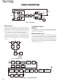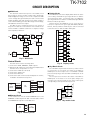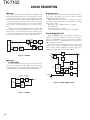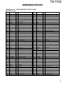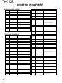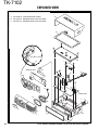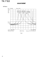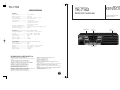
1
TK-7102
TK-7102
VHF FM TRANSCEIVER
SPECIFICATIONS
TK-7102
SERVICE MANUAL
GENERAL
Frequency Range ................................ 146 to 174MHz
© 2001-5 PRINTED IN JAPAN
B51-8584-00 (S) 283
Number of Channels ........................... 4 channels
Channel Spacing ................................. Wide : 25kHz
Narrow : 12.5kHz
PLL Channel Stepping ........................ 2.5, 5, 6.25, 7.5kHz
Operating Voltage ............................... 13.6V DC ±15%
Current Drain ...................................... Less than 0.4A on standby
Less than 1.0A on receive
Less than 8.0A on transmit
Operating Temperature Range ........... –30°C to +60°C
Dimensions & Weight ........................ 160 (W) x 43 (H) x 107 (D) mm, Approx 1.0kg
Channel Frequency Spread ................ 28MHz
RECEIVER (Measurements made per EIA standard EIA/TIA-603)
Sensitivity (12dB SINAD) .................... Wide : 0.28µV
Cabinet
(A01-2178-02)
Front glass
(B10-2668-03)
Narrow : 0.35µV
Selectivity ........................................... Wide : 75dB
Narrow : 65dB
Intermodulation ................................... Wide : 70dB
Narrow : 60dB
Spurious Response ............................. 75dB
Audio Power Output ........................... 4.0W
Frequency Stability ............................. ±2.5ppm
TRANSMITTER (Measurements made per EIA standard EIA/TIA-603)
RF Power Output ................................ 25W
Spurious and Harmonics ..................... 70dB
Modulation .......................................... Wide : 16K0F3E
FM Noise ............................................ Wide : 45dB
Narrow : 11K0F3E
Narrow : 40dB
Audio Distortion .................................. Less than 3%
Frequency Stability ............................. ±2.5ppm
KENWOOD
CORPORATION
14-6, Dogenzaka 1-chome, Shibuya-ku, Tokyo 150-8501, Japan
KENWOOD SERVICE CORPORATION
KENWOOD ELECTRONICS ITALIA S.p.A.
P.O. BOX 22745, 2201 East Dominguez Street, Long Beach, CA 90801-5745,
U.S.A.
Via G. Sirtori, 7/9 20129 Milano, Italy
KENWOOD ELECTRONICS CANADA INC.
Bolivia, 239-08020 Barcelona, Spain
6070 Kestrel Road, Mississauga, Ontario, Canada L5T 1S8
KENWOOD ELECTRONICS AUSTRALIA PTY. LTD.
KENWOOD ELECTRONICS DEUTSCHLAND GMBH
Rembrücker Str. 15, 63150 Heusenstamm, Germany
(A.C.N. 001 499 074)
16 Giffnock Avenue, Centrecourt Estate, North Ryde, N.S.W. 2113, Australia
KENWOOD ELECTRONICS BELGIUM N.V.
KENWOOD ELECTRONICS (HONG KONG) LTD.
Mechelsesteenweg 418 B-1930 Zaventem, Belgium
Unit 3712-3724, Level 37, Tower one Metroplaza, 223 Hing Fong Road, Kwai Fong, N.T.,
Hong Kong
KENWOOD ELECTRONICS FRANCE S.A.
13, Boulevard Ney, 75018 Paris, France
KENWOOD ELECTRONICS U.K. LIMITED
KENWOOD House, Dwight Road, Watford, Herts., WD1 8EB United Kingdom
KENWOOD ELECTRONICS EUROPE B.V.
Amsterdamseweg 37, 1422 AC Uithoorn, The Netherlands
KENWOOD IBERICA S.A.
KENWOOD ELECTRONICS TECHNOLOGIES(S) PTE LTD.
Sales Marketing Division
1 Ang Mo Kio Street 63, Singapore 569110
Key top
(K29-9065-01)
Panel assy
(A62-0942-03)
TK-7102
TK-7102
TERMINAL FUNCTION
CONTENTS / GENERAL
CONTENTS
GENERAL
GENERAL ................................................................. 2
INTRODUCTION
OPERATING FEATURES ......................................... 4
SCOPE␣ OF␣ THIS␣ MANUAL
REALIGNMENT ........................................................ 7
DISASSEMBLY FOR REPAIR .................................. 9
CIRCUIT DESCRIPTION ......................................... 10
SEMICONDUCTOR DATA ..................................... 15
DESCRIPTION OF COMPONENTS ....................... 16
PARTS LIST ............................................................ 18
EXPLODED VIEW ................................................... 24
PACKING ................................................................. 25
ADJUSTMENT ........................................................ 26
This manual is intended for use by experienced technicians familiar with similar types of commercial grade communications equipment. It contains all required service information for the equipment and is current as of this publication date. Changes which may occur after publication are
covered by either Service Bulletins or Manual Revisions,
which are issued as required.
ORDERING␣ REPLACEMENT␣ PARTS
When ordering replacement parts or equipment information, the full part identification number should be included.
This applies to all parts : components, kits, and chassis. If
the part number is not known, include the chassis or kit
number of which it is a part and a sufficient description of
the required component for proper identification.
PC BOARD VIEWS
DISPLAY UNIT (X54-3340-20) ........................... 31
TX-RX UNIT (X57-6290-20) ............................... 33
SCHEMATIC DIAGRAM ......................................... 39
BLOCK DIAGRAM................................................... 43
LEVEL DIAGRAM .................................................... 45
TERMINAL FUNCTION .......................................... 47
SPECIFICATIONS................................. BACK COVER
PERSONNEL␣ SAFETY
The following precautions are recommended for personnel safety :
• DO␣ NOT␣ transmit if someone is within two feet (0.6
meter) of the antenna.
• DO␣ NOT␣ transmit until all RF␣ connectors are secure and
any open connectors are properly terminated.
• SHUT␣ OFF this equipment when near electrical blasting
caps or while in an explosive atmosphere.
• All equipment should be properly grounded before
power-up for safe operation.
• This equipment should be serviced by only qualified technicians.
CN1 (TX-RX Unit)
Pin No.
1
2
3
4
5
6
7
8
9
10
11
12
13
14
15
16
17
18
19
20
21
22
23
Name
GND
PTT
HOOK
ME
MIC
POWER
LED MON
LED PF
LED C1
LED C2
LED R
LED G
MICBL
LED C3
LED C4
CM
KM11
KM12
KM13
KM14
KM01
KM02
PSB
Function
Ground
PTT/TXD
Hook detection/RXD
Mic ground
Mic signal input
Power switch
Signal of MON Key control
Signal of PF Key control
Signal of channel1 control
Signal of channel2 control
Signal of TX control
Signal of Busy control
Mic backlight control
Signal of channel3 control
Signal of channel4 control
Mic data detection
Key matrix input 11
Key matrix input 22
Key matrix input 33
Key matrix input 44
Key matrix input 01
Key matrix input 02
Switched B
J1 (TX-RX Unit)
Pin No.
1
2
Name
SP
E
Function
Audio signal output to internal/external speaker.
Ground
J1 (Control Unit)
Pin No.
1
2
3
4
5
6
7
8
Name
MBL
PSB
GND
PTT/TXD
ME
MIC
HOOK/RXD
CM
Function
MIC backlight control.
13.6V.
Ground.
PTT.
MIC ground.
MIC signal input.
Hook detection
MIC data detection.
PRE-INSTALLATION␣ CONSIDERNATIONS
1. UNPACKING
Unpack the radio from its shipping container and check
for accessory items. If any item is missing, please contact
KENWOOD␣ immediately.
2. LICENSING␣ REQUIREMENTS
Federal regulations require a station license for each radio installation (mobile or base) be obtained by the equipment owner. The licensee is responsible for ensuring transmitter power, frequency, and deviation are within the limits
permitted by the station license.
Transmitter adjustments may be performed only by a licensed technician holding an FCC␣ first, second or general
class commercial radiotelephone operator’s license. There
is no license required to install or operate the radio.
22
47
TK-7102
GENERAL
3. PRE-INSTALLATION␣ CHECKOUT
3-1. Introduction
5. INSTALLATION␣ PLANNING – CONTROL␣ STATIONS
5-1. Antenna system
Each radio is adjusted and tested before shipment. However, it is recommended that receiver and transmitter operation be checked for proper operation before installation.
Control station. The antenna system selection depends
on many factors and is beyond the scope of this manual.
Your KENWOOD␣ dealer can help you select an antenna system that will best serve your particular needs.
3-2. Testing
The radio should be tested complete with all cabling and
accessories as they will be connected in the final installation. Transmitter frequency, deviation, and power output
should be checked, as should receiver sensitivity, squelch
operation, and audio output. Signalling␣ equipment operation
should be verified.
4. PLANNING␣ THE␣ INSTALLATION
4-1. General
Inspect the vehicle and determine how and where the
radio antenna and accessories will be mounted.
Plan cable runs for protection against pinching or crushing wiring, and radio installation to prevent overheating.
4-2. Antenna
The favored location for an antenna is in the center of a
large, flat conductive area, usually at the roof center. The
trunk lid is preferred, bond the trunk lid and vehicle chassis
using ground straps to ensure the lid is at chassis ground.
5-2. Radio location
Select a convenient location for your control station radio
which is as close as practical to the antenna cable entry
point. Secondly, use your system’s power supply (which
supplies the voltage and current required for your system).
Make sure sufficient air can flow around the radio and power
supply to allow adequate cooling.
SERVICE
This radio is designed for easy servicing. Refer to the
schematic diagrams, printed circuit board views, and alignment procedures contained in this manual.
NOTE
If you do not intend to use the 3.5-mm jack for the external speaker, fit the supplied speaker-jack cap to stop dust
and sand getting in.
4-3. Radio
The universal mount bracket allows the radio to be
mounted in a variety of ways. Be sure the mounting surface
is adequate to support the radio’s weight. Allow sufficient
space around the radio for air cooling. Position the radio
close enough to the vehicle operator to permit easy access
to the controls when driving.
4-4. DC␣ Power and wiring
1. This radio may be installed in negative ground electrical
systems only. Reverse polarity will cause the cable fuse
to blow. Check the vehicle ground polarity before installation to prevent wasted time and effort.
2. Connect the positive power lead directly to the vehicle
battery positive terminal. Connecting the Positive lead to
any other positive voltage source in the vehicle is not recommended.
3. Connect the ground lead directly to the battery negative
terminal.
4. The cable provided with the radio is sufficient to handle
the maximum radio current demand. If the cable must be
extended, be sure the additional wire is sufficient for the
current to be carried and length of the added lead.
Antenna connector
speaker jack cap
Power input
connector
3
TK-7102
OPERATING FEATURES
1-4. Display
1. Controls and Functions
1-1. Front Panel
q we
rt
i
u
y
1-2. Microphone
Indicator
o
q
w
e
r
t
y
u
i
o
(Power) switch
Press to switch the transceiver ON. Press and hold for
approximately 1 seconds to switch the transceiver OFF.
▲ key
Press to increase the volume level.
▼ key
Press to decrease the volume level.
● key
PF (Programmable Function) key. The default setting of
this key is None (no function). The programmable functions available for this key are listed below.
key
PF (Programmable Function) key. The default setting of
this key is Monitor (page 5). Other programmable functions available for this key are listed below.
1/ 2/ 3/ 4 keys
Press to select a channel from 1 to 4.
Microphone jack
Insert the microphone plug into this jack (the microphone is an optional accessory).
Speaker
Internal speaker.
PTT switch
Press this switch, then speak into the microphone to call
a station.
1-3. Auxiliary Programmable Functions:
• Emergency
• Scan On/OFF
• Key Lock
• Talk Around
• Monitor
• Temporary Delete
• None (no function)
4
Description
Light while transmitting.
Lights when a signal is detected on
the currently selected channel.
L i g h t s w h i l e t h e f u n ct i o n p r o grammed onto its corresponding key
is activated.
L i g h t s w h i l e t h e f u n ct i o n p r o grammed onto its corresponding key
is activated.
Lights to display the currently selected channel (1~ 4)
1-5. Rear panel
Antenna connector
External
speaker jack
Power input
connector
TK-7102
OPERATING FEATURES
2. Operation Features
• Scan ON/OFF
The TK-7102 is a VHF FM radio designed to operate in
conventional format. The programmable features are summarized.
• Talk around
3. Transceiver Controls and Indicators
3-1. Front Panel Controls
All the keys on the front panel are momentary-type push
buttons. The functions of these keys are explained below.
• POWER key
Press this key starts scanning. Pressing this key stops
scanning.
Press this key, the transceiver uses the receive frequency and the tone for transmission.
The operator can call the other party directly (without repeater). Press this key again, the talk around function goes
off.
• Temporary delete
• CHANNEL keys
The "Add" channel contained in the scan sequence, and
"Delete" channel is not contained. In the scan mode, this
key switches the channel delete temporarily (Press and hold
for approximately one second).
When the transceiver is turned off, the transceiver exits
the scan or switches the scan function off.
• MONITOR key (Programmable)
• None
•
• VOLUME UP/DOWN key
Sounds error operation beep, and no action will occur.
Use this function when the transceiver is required to be
more simple operated.
When the key is pressed, the volume level is increased/
decreased and repeats if held for 200ms or longer.
4. Scan Operating
• BUSY/TX LED
■ SCAN start condition
The BUSY indicator (Green LED) shows that the channel
is in use. The TX indicator (Red LED) shows that you are
transmitting.
Two or more channels must be added to all channels that
can be scanned. The transceiver must be in normal receive
mode (PTT off).
When you activate the key programmed to the scan ON/
OFF function, the scan starts. The indicator next to the programmed key LED blinks.
Transceiver POWER key. When the power is switched
off, all the parameters are stored in memory. When the
power is switched on again, the transceiver returns to the
previous conditions.
key (Programmable)
3-2. Programmable Keys
The FPU (KPG-70D) enables programmable keys to select the following functions.
• Emergency
• Key Lock
• Monitor
• Scan ON/OFF
• Talk Around
• Temporary Delete
• None
• Emergency
Pressing this key for longer than 1 second causes the
transceiver to enter the emergency mode. The transceiver
jumps to the programmed "Emergency channel" and transmits for 25* seconds.
The transceiver disables mic mute while transmitting.
After finishing transmission, the transceiver receivers for 5*
seconds. The transceiver Mute* the speaker while receiving. Following the above sequence, the transceiver continues to transmit and receive.
* Default value.
• Key lock
Pressing this key causes the transceiver to accept entry
of only the [Vol Up/Down]*, [Key lock], Microphone [PTT],
[Monitor], [Emergency], and [Power] keys.
* Programmable
• Monitor
Used to release signalling (press once) or squelch (press
and hold for approximately two seconds) when operating as
a conventional. It is also used to reset option signalling.
■ Scan stop condition
The scan stops temporarily if the following conditions are
satisfied.
1) A carrier is detected, then QT/DQT matches on channels
for which receive the QT/DQT is set by the programming
software.
2) A carrier is detected on the channels for which receiving
QT/DQT is not set by the programming software or when
the monitor (signalling cancel) function is activated.
■ Revert channel
The revert channel is used to transmit during scanning
and set by the programming software (KPG-70D).
1) Selected channel
The transceiver reverts to the channel before scanning or
the channel that you changed during scan.
2) Selected with talkback
The transceiver reverts to the selected channel prior to
scan initiation.
However, if a call is received on a channel other then the
selected channel and PTT is pressed before scanning resume, the transceiver "talks back" on the current receive
channel.
■ Scan end
When you press the key programmed to the scan function during scan mode, the scan ends.
The indicator next to the programmed key LED turns off.
5
TK-7102
OPERATING␣ FEATURES
■ Temporary delete
■ Clear to transpond
It is possible to delete channel temporary during scan.
When scan stops on unnecessary channel for example by
interference of the other party, activate the delete function
(for example press and hold the key for approximately one
second), then that channel is deleted temporarily and scan
re-start immediately.
The temporary deleted channels return to pre-set delete/
add channels, when the transceiver is turned off or the scan
function is switched off.
The transceiver waits the transpond of DTMF if channel
is busy until channel open. This feature prevents the interference to other party.
5. Details of Features
■ Time-out timer
The time-out timer can be programmed in 30 seconds
increments from 30 seconds to five minutes and off. If the
transmitter is transmitted continuously for longer than the
programmed time, the transmitter is disabled and a warning
tone sounds while the PTT button is held down. The warning tone stops when the PTT button is released.
■ PTT ID
PTT ID provides a DTMF ANI to be sent with every time
PTT (beginning of transmission, end of transmission, or
both).
You can program PTT ID "on" or "off" for each channel.
The contents of ID are programmed each Radio.
The timing that the transceiver sends ID is programmable.
BOT : DTMF ID (Beginning of TX) is sent on beginning of
transmission.
EOT : DTMF ID (End of TX) is sent on end of transmission.
Both : DTMF ID (Beginning of TX) is sent on beginning of
transmission and DTMF ID (End of TX) is sent on end of
transmission.
■ Off hook decode
If the Off hook decode function has been enabled, removing and replacing the microphone on the hook has no
effect for decoding QT/DQT and option signalling.
■ "TOT" pre-alert
The transceiver has "TOT" pre-alert timer. This parameter
selects the time at which the transceiver generates "TOT"
pre-alert tone before "TOT" is expired.
"TOT" will be expired when the selected time passes
from a TOT pre-alert tone.
■ "TOT" re-key time
The transceiver has "TOT" re-key timer. This timer is the
time you can not transmit after "TOT" exceeded. After "TOT"
re-key time expired you can transmit again.
■ "TOT" reset time
The transceiver has "TOT" reset timer. This timer is the
minimum wait time allowed during a transmission that will
reset the "TOT" count.
"TOT" reset time causes the "TOT" to continue even after
PTT is released unless the "TOT" reset timer has expired.
6
6. Option Signalling (DTMF)
Built-in DTMF decoder is available for option signalling.
It is possible to use individual call, group call, Stun.
If the option signalling matches, a predetermined action
will occur.
If option signalling matches on a channel is set up with
option signalling, the channel LED will flash and option signalling will be released. The transpond or alert tone will
sound.
While option signalling matches (or if option signalling is
deactivated when you are transmitting), you can mute or
unmute QT/DQT/Carrier.
■ SP Unmute
You can select the type of SP Unmute system for each
channel. The selection is as follows.
Carrier, QT/DQT:
Channel with this option will not check ID Code in order
to open its speaker.
Carrier+DTMF, QT/DQT+DTMF:
Channel that is set with this option will have to check for
ID Code in order to open its speaker.
Default:
Carrier, QT/DQT.
SP Unmute
Channel Setting
RX Condition
QT/DQT DTMF
None Carrier
Carrier
None
Carrier
Yes
Carrier+DTMF
Carrier
Carrier+DTMF None
Yes
Carrier+DTMF
Carrier
None
Carrier+QT/DQT
Carrier
QT/DQT
Yes
Carrier+QT/DQT
Yes
Carrier+QT/DQT+DTMF
Carrier+DTMF
Carrier
Carrier+QT/DQT
QT/DQT+DTMF Yes
Yes
Carrier+QT/DQT+DTMF
Carrier+DTMF
Speaker
Condition
Sounds
Sounds
Sounds
Not Sounds
Sounds
Not Sounds
Sounds
Not Sounds
Sounds
Sounds
Not Sounds
Not Sounds
Not Sounds
Sounds
Not Sounds
Note:
When QT/DQT is not used, QT/DQT and QT/DQT+DTMF
can not be selected.
When DTMF is not used, Carrier+DTMF and QT/
DQT+DTMF can not be selected.
■ Auto Reset
If option signalling matches a group set up with option
signalling, option signalling is released. After matching option signalling, option signalling will temporarily reset automatically.
TK-7102
OPERATING␣ FEATURES / REALIGNMENT
■ Stun
If the stun code matches, a predetermined action will occur. Whether option signalling is activated or not, when
stun matches on any channel, the transceiver will become
TX inhibited or TX/RX inhibited. While stun is active, if the
stun code + "#" code is received, stun will deactivate.
When stun matches, transpond will function. Alert will
not be output.
7. Audible User Feedback Tones
The transceiver outputs various combinations of tones to
notify the user of the transceiver operating state.
Refer to the help file on the KPG-70D, regarding the functions that are not listed below.
REALIGNMENT
1. Modes
User mode
PC mode
Data programming mode
Clone mode
PC test mode
Mode
User mode
PC mode
■ Stun on tone
When a stun code is received, transpond tone sounds.
■ Stun off tone
When a stun release code is received, transpond tone
sounds.
■ Group call tone
Sounds when a group call with the correct DTMF option
signalling is received, repeats 7 times. You can select yes or
no in the Alert tone level setting.
■ Individual call tone
Sounds when an individual call with the correct DTMF
option signalling is received. You can select yes or no in the
Alert tone level setting.
■ Key input error tone
Sounds when a key is pressed but that key cannot be
used. You can select yes or no for the optional feature's
warning tone.
■ Transpond tone
Sounds when an individual call with the correct DTMF
option signalling is received. For group calls, only the group
tone will sound, not the transpond tone.
Data programming
mode
PC test mode
PC tuning mode
Clone mode
PC tuning mode
Function
For normal use.
Used for communication between the
radio and PC (IBM compatible).
Used to read and write frequency data
and other features to and from the radio.
Used to check the radio using the PC.
This feature is included in the FPU.
Used to tune the radio using the PC.
Used to transfer programming data from
one radio to another.
2. How to Enter Each Mode
Mode
User mode
PC mode
Clone mode
Operation
Power ON
Received commands from PC
[1]+Power ON (Two seconds)
3. PC Mode
3-1. Preface
The TK-7102 transceiver is programmed using a personal
computer, a programming interface (KPG-46) and programming software (KPG-70D).
The programming software can be used with an IBM PC
or compatible. Figure 1 shows the setup of an IBM PC for
programming.
3-2. Connection Procedure
■ Pre alert tone
Sounds prior to the TOT TX inhibit activation. If TOT pre
alert is set, the tone sounds at the amount of time programmed, before the TOT expires (TOT time – TOT pre alert
time = Pre alert tone sounding time). You can select yes or
no for the optional feature's warning tone.
1. Connect the TK-7102 to the personal computer with the
interface cable.
2. When the Power is switched on, user mode can be entered immediately. When the PC sends a command, the
radio enters PC mode.
When data is transmitted from transceiver, the red LED
blink.
When data is received by the transceiver, the green LED
blink.
In the PC mode, 4CH LEDs, [MON] LED and [ ] LED are
turned on.
Notes :
• The data stored in the personal computer must match
model type when it is written into the EEPROM.
• Attach the interface cable, then change the TK-7102 to
PC mode.
7
TK-7102
REALIGNMENT
3-3. KPG-46 Description
(PC programming interface cable : Option)
The KPG-46 is required to interface the TK-7102 to the
computer. It has a circuit in its D-subconnector (25-pin) case
that converts the RS-232C logic level to the TTL level.
The KPG-46 connects the modular microphone jack of
the TK-7102 to the computers RS-232C serial port.
KPG-46
IBM-PC
KPG-70D
Fig. 1
Adding the data password.
If the data password is set in the optional feature menu,
you must enter the password (Master transceiver) to activate a clone mode.
you can use 1, 2, 3, and 4 to configure the password. The
maximum length of the password is 10 digits.
1. [1]+Power ON.
2. [1]~[4] LED, and MON LED are turned ON.
3. Enter the password using [1]~[4] keys.
4. Press [MON] key.
5. If the password matches, the transceiver enters a clone
mode. Otherwise, transceiver beeps and returns to the
password input mode.
TK-7102
3-4. Programming Software Description
The KPG-70D programming disk is supplied in 3-1/2" disk
format. The software on this disk allows a user to program
TK-7102 radio via a programming interface cable (KPG-46).
3-5. Programming With IBM PC
If data is transferred to the transceiver from an IBM PC
with the KPG-70D, the destination data (basic radio information) for each set can be modified.
4. Clone Mode
Programming data can be transferred from one radio to
another by connecting them via their modular microphone
jacks. The operation is as follows (the transmit radio is the
master and the receive radio is the slave).
NOTE: Clone mode should enabled.
1. Turn the master TK-7102 power ON with the [1] key held
down. The TK-7102 [ ] LED is turned on.
2. Power on the slave TK-7102.
3. Connect the cloning cable (No. E30-3382-05) to the
modular microphone jacks on the master and slave.
4. Press the [ ] key on the master TK-7102 transceiver. The
data of the master is sent to the slave. While the master
is sending data, [TX] LED blinked. While the slave is receiving the data, 4 LEDs, [MON] LED, [ ] LED are turned
on and [BUSY] LED blinked. When cloning of data is completed, the master [TX] LED turned off, and the slave automatically operates in the User mode. The slave can
then be operated by the same program as the master.
5. The other slave can be continuously cloned. Carry out
the operation in step 2 to 4.
8
Cloning cable
(E30-3382-05)
Fig. 2
TK-7102
DISASSEMBLY FOR REPAIR
1. When you remove the panel, turn the transceiver up
side down. Detach the panel by lifting the tabs as
shown below.
3. To remove the display unit PCB, detach the PCB by
lifting at the indents of the PCB as shown below.
tabs
indents
Fig. 1
Fig. 3
2. To remove the cabinet, first turn the transceiver up
side down. Detach the cabinet by prying the tabs as
shown below.
4. When mounting the front panel, match the 4 tabs of
the chassis with the panel, being sure they attach
securely.
tabs
tabs
tabs
tabs
Fig. 2
Fig. 4
9
TK-7102
CIRCUIT DESCRIPTION
■ IF Amplifier
Frequency Configuration
The first IF signal is amplified by Q19, and the enters IC5
(FM processing IC). The signal is heterodyned again with a
second local oscillator signal within IC5 to create a 450kHz
second IF signal. The second IF signal is then fed through a
450kHz ceramic filter (Wide : CF1, Narrow : CF2) to further
eliminate unwanted signals before it is amplified and FM detected in IC5.
The receiver utilizes double conversion. The first IF is
49.95MHz and the second IF is 450kHz. The first local oscillator signal is supplied from the PLL circuit.
The PLL circuit in the transmitter generates the necessary frequencies. Figure 1 shows the frequencies.
ANT
CF 450kHz
1st
MCF
MIX 49.95MHz
ANT
SW
RF
AMP
IF SYSTEM
AF
AMP
Item
Nominal center frequency
Pass bandwidth
35dB stop bandwidth
Ripple
Insertion loss
Guaranteed attenuation
SP
50.4MHz
X3
multiply
16.8MHz
TCXO
RX
PA
AMP
1/2
TX
AMP
PLL/VCO
TX
Fig. 1
MIC
AMP
Terminal impedance
MIC
Table 1
Frequency configuration
The receiver is double conversion superheterodyne. The
frequency configuration is shown in Figure 1.
■ Front-end RF Amplifier
An incoming signal from the antenna is applied to an RF
amplifier (Q26) after passing through a transmit/receive
switch circuit (D31 is off) and a band pass filter (L36, L38
and varactor diodes: D25, D26). After the signal is amplified
(Q26), the signal is filtered through a band pass filter (L30,
L32 and varactor diodes: D21, D22) to eliminate unwanted
signals before it is passed to the first mixer.
The voltage of these diodes are controlled by tracking the
CPU (IC6) center frequency of the band pass filter. (See Fig.
2)
Table 2
The signal from the RF amplifier is heterodyned with the
first local oscillator signal from the PLL frequency synthesizer circuit at the first mixer (Q21) to create a 49.95MHz
first intermediate frequency (1st IF) signal. The first IF signal
is then fed through two monolithic crystal filters (MCFs :
XF1) to further remove spurious signals.
Table 3
D30,31
ANT
SW
CF2 (Narrow)
Q21
MIX
XF1
MCF
IC23
1/2 divider
CPU
Q19
IF AMP
X1
TCXO
1st local
OSC (VCO/PLL)
Fig. 2
10
Ceramic filter (L72-0994-05) : CF2
IC3
AF AMP
IC5
MIX,IF,DET
TV
IC3
D/A
Rating
450kHz
± 4.5kHz or more
± 10.0kHz or less
2.0dB or less
6.0dB or less
55.0dB or more within fo± 100kHz
2.0kΩ
CF1 (Wide)
ANT
L30,32
Q26 D21,22
RF AMP BPF
Rating
450kHz
± 6.0kHz or more
± 12.5kHz or less
2.0dB or less
6.0dB or less
35.0dB or more within fo± 100kHz
2.0kΩ
Ceramic filter (L72-0993-05) : CF1
Item
Nominal center frequency
6dB bandwidth
50dB bandwidth
Ripple
Insertion loss
Guaranteed attenuation
Terminal impedance
■ First Mixer
L36,38
D25,26
BPF
Crystal filter (L71-0591-05) : XF1
Item
Nominal center frequency
6dB bandwidth
50dB bandwidth
Ripple
Insertion loss
Guaranteed attenuation
Terminal impedance
Receiver System
Rating
49.95MHz
± 5.0kHz or more at 3dB
± 20.0kHz or less
1.0dB or less
5.0dB or less
80dB or more at fo± 1MHz
Spurious : 40dB or more within fo± 1MHz
350Ω / 5.5pF
Receiver system
Q6
X3 multiply
DEO
TK-7102
CIRCUIT DESCRIPTION
■ Wide/Narrow Changeover Circuit
■ Squelch Circuit
The Wide port (pin 92) and Narrow port (pin 91) of the
CPU is used to switch between ceramic filters. When the
Wide port is high, the ceramic filter SW diodes (D13, D15)
cause CF1 to turn on to receive a Wide signal.
When the Narrow port is high, the ceramic filter SW diodes
(D13, D15) cause CF2 to turn on to receive a Narrow signal.
The detection output from the FM IF IC (IC5) passes
through a noise amplifier (Q18) to detect noise. A voltage is
applied to the CPU (IC6). The CPU controls squelch according to the voltage (SQIN) level. The signal from the RSSI pin
of IC5 is monitored. The electric field strength of the receive signal can be known before the SQIN voltage is input
to the CPU, and the scan stop speed is improved.
IC5
IF System
IF_IN
IC5
R73
Wide
IC6 92pin
CF1
(Wide)
R77
AF
D18
DET
IF
SYSTEM RSSI
D15
Fig. 5
IC6
SQIN
RSSI
CPU
Squelch circuit
R78
CF2
(Narrow)
R74
D13
Q18
NOISE AMP
MIX_O
Narrow
IC6 91pin
Fig. 3
PLL Frequency Synthesizer
Wide/Narrow changeover circuit
The PLL circuit generates the first local oscillator signal
for reception and the RF signal for transmission.
■ AF Signal System
The detection signal from IF IC (IC5) goes to AF amp (IC3)
to adjust the gain and is output to AF filter (IC10) for characterizing the signal. The AF signal output from IC10 and the
DTMF signal, BEEP signal are summed and the resulting signal goes to the D/A converter (IC3). The AFO output level is
adjusted by the D/A converter. The signal output from the
D/A converter is input to the audio power amplifier (IC16).
The AF signal from IC16 switches between the internal
speaker and speaker jack (J1) output.
IC5
IF IC
IC3
AF DEO
AMP
FIg. 4
IC10
IC3
IC102
AF
Filter
D/A
CONV.
AF PA
AF signal system
SP
■ PLL
The frequency step of the PLL circuit is 5 or 6.25kHz. A
16.8MHz reference oscillator signal is divided at IC1 by a
fixed counter to produce the 5 or 6.25kHz reference frequency. The voltage controlled oscillator (VCO) output signal is buffer amplified by Q15, then divided in IC1 by a dualmodule programmable counter. The divided signal is compared in phase with the 5 or 6.25kHz reference signal in the
phase comparator in IC1. The output signal from the phase
comparator is filtered through a low-pass filter and passed
to the VCO to control the oscillator frequency. (See Fig. 6)
■ VCO
The operating frequency is generated by Q11 in transmit
mode and Q10 in receive mode. The oscillator frequency is
controlled by applying the VCO control voltage, obtained
from the phase comparator, to the varactor diodes (D10 and
D12 in transmit mode and D9 and D11 in receive mode).
The TX/RX pin is set low in receive mode causing Q12 and
Q7 to turn Q11 off, and turn Q10 on. The TX/RX pin is set
high in transmit mode. The outputs from Q10 and Q11 are
amplified by Q15 and sent to the buffer amplifiers.
11
TK-7102
CIRCUIT DESCRIPTION
IC1 : PLL IC
1/N
Q11
TX VCO
5kHz/6.25kHz
Q3
RF AMP
Q15
BUFF
AMP
LPF
Phase
comparator
PLL
DATA
D10,12
Charge
pump
Q10
RX VCO
REF
OSC
1/M
Q7,12
T/R SW
5kHz/6.25kHz
D9,11
16.8MHz
Fig. 6
PLL circuit
■ Unlock Circuit
Transmitter System
During reception, the 8RC signal goes high, the 8TC signal goes low, and Q29 turns on. Q31 turns on and a voltage
is applied to the collector (8R). During transmission, the
8RC signal goes low, the 8TC signal goes high and Q30
turns on. Q33 turns on and a voltage is applied to 8T.
The CPU in the control unit monitors the PLL (IC1) LD
signal directly. When the PLL is unlocked during transmission, the PLL LD signal goes low. The CPU detects this
signal and makes the 8TC signal low. When the 8TC signal
goes low, no voltage is applied to 8T, and no signal is transmitted.
■ Outline
The transmitter circuit produces and amplifies the desired frequency directly. It FM-modulates the carrier signal
by means of a varicap diode.
■ Power Amplifier Circuit
The transmit output signal from the VCO passes through
the transmission/reception selection diode (D19) and amplified to a specified level of the power module (IC101) by the
drive block (Q23 and Q25). The amplified signal goes to a
low-pass filter. The low-pass filter removes unwanted highfrequency harmonic components, and the resulting signal is
goes the antenna terminal.
8C
8R
Q31
SW
Q33
SW
Q29
SW
Q30
SW
8RC
8T
8TC
IC6
CPU
LD
IC1
PLL
PLL lock
: LD "H"
Fig. 7
MIC
Unlock circuit
IC21(1/2)
MIC/IDC
NJM2100V
IC22
Splatter
FILTER
NJM2904V
IC6
MIC KEY
INPUT
CPU
784214GC
IC3
D/A
CONVERTER
M62363FP
X1
TCXO
16.8MHz
IC4
SUM AMP
NJM2902V
Q15
BUFFER
2SC5108
(Y)
IC1
Q3
BUFFER
2SC4649
(N,P)
ANT
IC23
1/2
DIVIDER
UPB1509GV
Fig. 8
12
IC4
BUFFER
NJM2902V
IC3
D/A
CONVERTER
M62363FP
Q11
VCO
2SK508NV
(K52)
PLL
MB15A02
IC3
D/A
CONVERTER
M62363FP
Q20
BUFFER
2SC4649
(N,P)
Q23
Q25
IC101
RF AMP
2SC3357
RF AMP
2SC2954
POWER AMP
M67741H-32
Transmitter system
TK-7102
CIRCUIT DESCRIPTION
■ APC Circuit
The automatic transmission power control (APC) circuit
detects part of a power module output with a diode (D34,
D36) and applies a voltage to IC12. IC12 compares the APC
control voltage (PC) generated by the D/A converter (IC3)
and DC amplifier (IC4) with the detection output voltage to
control Q27 and Q28, generates DB voltage from B voltage,
and stabilizes transmission output.
The APC circuit is configured to protect over current of
the power module due to fluctuations of the load at the antenna end and to stabilize transmission output at voltage
and temperature variations.
■ Display Circuit
The CPU (IC6) controls the display LEDs. When the transceiver is busy, the LEDG line goes high, Q4 turns on and the
green LED (D11) lights. In transmit mode, the LEDR line
goes high, Q8 turns on and the red LED (D12) lights. Backlit
LEDs (D1~D4) are provided.
When a function key (MON, PF, C1, C2, C3 or C4) is selected, its respective line goes high (LED MON, LED PF,
LED C1, LED C2, LED C3 or LED C4), the switch connected
to that line turns on and the amber LED lights.
LEDMON
Q1
SW
LEDPF
Q5
SW
LEDC1
Q2
SW
LEDC2
Q6
SW
LEDC3
Q3
SW
LEDC4
Q7
SW
LEDG
Q4
SW
LEDR
Q8
SW
MICBL
Q10
SW
ANT
D19
Q23
Q25
IC101
D30,31
RF
AMP
RF
AMP
POWER
MODULE
ANT
SW
LPF
DB
Q28
+B
POWER
DET
Q27
PRI
DRIVER
IC12
IC4
PC
IC3
3pin
APC
CONTROL
DC
AMP
Fig. 9
APC circuit
IC6 CPU
APC
DRIVER
D34,36
D5
D6
D7
D8
D9
D10
D11
D12
Q9
SW
D1~4
Control Circuit
The CPU carries out the following tasks:
1) Controls the WIDE, NARROW, TX/RX outputs.
2) Adjusts the AF signal level of the AF filter (IC10) and turns
the filter select compounder on or off.
3) Controls the DTMF decoder (IC9).
4) Controls the display unit.
5) Controls the PLL (IC1).
6) Controls the D/A converter (IC3) and adjusts the volume,
modulation and transmission power.
The TK-7102 front panel has function keys. Each of them
is connected to a cross point of a matrix of the KMI1 to
KMO2 ports of the microprocessor. The KMO1 to KMO2
ports are always high, while the KMI1 to KMI4 ports are always low.
The microprocessor monitors the status of the KMI1 to
KMO2 ports. If the state of one of the ports changes, the
microprocessor assumes that the key at the matrix point
corresponding to that port has been pressed.
PF
MON
KMI4
C4
The transceiver has an 8k-bit EEPROM (IC7). The
EEPROM contains adjustment data. The CPU (IC6) controls
the EEPROM through three serial data lines.
IC6
CPU
C3
Control circuit
KMI1
KMI2
KMI3
VOL
DN
IC1
PLL
VOL
UD
PLLE
DT
CK
■ Key Matrix Circuit
C2
Fig. 10
■ Memory Circuit
IC6
CPU
IC3
D/A
converter
Display circuit
C1
IC9
DTMF
DECO.
DTMDAT
DTMCLK
DTMSTD
CNTCK
CNTDT
DAST
Fig. 12
KMO2
KMO1
Fig. 13
Key matrix circuit
EEPCK
IC6
CPU
Fig. 11
EEPDT
EEPWP
IC7
EEPROM
Memory circuit
13
TK-7102
CIRCUIT DESCRIPTION
■ Encode
■ D/A Converter
The QT and DQT signals are output from QT/DQT of the
CPU (IC6) and summed with the external pin DI line by the
summing amplifier (IC4) and the resulting signal goes to the
D/A converter (IC3). The DTMF signal is output from DTMF
of the CPU and goes to the D/A converter (IC3). The signal
is summed with a MIC signal by the summing amplifier
(IC4), and the resulting signal goes to the D/A converter
(IC3).
The D/A converter (IC3) adjusts the MO level and the balance between the MO and QT/DQT levels. Part of a QT/
DQT signal is summed with MO and the resulting signal
goes to the VCOMOD pin of the VCO. This signal is applied
to a varicap diode in the VCO for direct FM modulation.
The D/A converter (IC3) is used to adjust MO modulation,
AF volume, TV voltage, FC reference voltage, and PC
POWER CONTROL voltage level.
Adjustment values are sent from the CPU as serial data.
The D/A converter has a resolution of 256 and the following
relationship is valid:
D/A output = (Vin – VDAref) / 256 x n + VDAref
Vin: Analog input
VDAref: D/A reference voltage
n: Serial data value from the microprocessor (CPU)
IC4
SUM
AMP
QT/DQT
IC6
CPU
DI
DTMF
IC4
SUM
AMP
IC3
D/A
TCXO
MOD
X1
TCXO
IC3
D/A
IC3
PLL
VCO
VCO
MOD
HT
Power Supply Circuit
When the POWER switch on the display unit is pressed,
the power port on the display unit which is connected to
CPU port 18 (POWER), goes low, then CPU port 93 (SBC)
goes high, Q34 turns on, SB SW (Q42) turns on and power
(SB) is supplied to the radio.
This circuit has an overvoltage protection circuit. If a DC
voltage of 18 V or higher is applied to the power cable, D39
turns on and a voltage is applied to the base of Q38. This
voltage turns Q38 on and turns Q34 and SB off.
Q42
SW
B
Fig. 14
Encode
IGN
Q16
SW
Q34
SW
The signal (DEO) passes through two low-pass filters of
IC11, goes to QTIN of the CPU (IC6) to decode QT, DQT.
The DTMF signal is decoded by a dedicated IC (IC9) and the
resulting signal is sent to the CPU (IC6) as serial data.
IC6
CPU
14
5M IC17
AVR
5M
POWER
RESET
IC15
RESET
Q18
INT
POWER
SW
IC11(1/2)
LPF
DEO
SD
IC9
STD
DTMF
ACK DECO.
Fig. 15
D39
SBC
IC6
CPU
INT
IC11(2/2)
LPF
QTIN
Q38
SW
IGN
■ Decode
• QT/DQT/DTMF
B
Fig. 16
Decode
Power supply circuit
TK-7102
SEMICONDUCTOR DATA
Microprocessor : 784214AGCXXX (TX-RX Unit IC6)
■ Terminal function
Pin No.
Name
I/O
1
NC
I
2
DTMOSC
O
3
PLLE
O
4
EVLLD
5
Function
Pin No.
Name
I/O
I/O
Function
48
FNC8
Function Port8
DTMF IC Clock Control
49
NC
I
PLL IC Chip Select
50
MUTE1
O
AF Mute
O
E-Volume LD
51
MUTE2
O
Speaker Mute
DTMCK
O
DTMF Dec IC Clock
52
MUTE3
O
AF AMP SW
6
DTMDT
I/O
DTMF Dec IC Data
53
DT
O
Common Data
7
UL
O
Unlock Detect
54
CK
O
Common Clock
8
BSHIFT
O
Clock Shift
55
NC
I
9
VDD
-
56
EEPCK
O
EEPROM Clock
10
X2
-
X’TAL(7.3728MHz)
57
EEPDT
I/O
EEPROM Data
11
X1
-
X’TAL(7.3728MHz)
58
EEPWT
O
EEP Write Protect
12
VSS
-
GND
59
DST1
I
Destination 1
13
NC
-
OPEN
60
DST2
I
Destination 2
14
NC
-
GND
61
DST3
I
Destination 3 (Open)
15
RESET
-
CPU RESET
62
NC
I
16
INT
I
uCOM Stop
63
24VDET
I
17
DMTSDT
I
DTMF Dec IC STD
64
NC
I
18
POWER
I
Power Key Input
65
LEDC1
O
19
IGN
I
Ignition
66
LEDC2
O
LED for CH2 Key
20
TX/RX
O
TX/RX
67
LEDR
O
TX LED
21
LEDMON
O
LED for MON Key
68
LEDG
O
Busy LED
22
LEDPF
O
LED for PF Key
69
MICBL
O
Mic Back Light
23
AVDD
-
+5V
70
LEDC3
O
LED for CH3 Key
24
AVREF
-
+5V
71
LEDC4
O
LED for CH4 Key
25
QTIN
I
QT/DQT Input
72
VSS
-
GND
26
SQIN
I
Squelch Input
73
MICMT
O
Mic1 Mute
27
RSSI
I
RSSI Input
74
MICEM
O
Mic2 Mute
28
PWRPRCT
I
Power Protect
75
NC
I
29
BATT
I
Battery Voltage
76
8RC
O
8R Control
30
TEMP1
I
Temperature1
77
8TC
O
8T Control
31
TEMP2
I
Temperature2
78
CM
I/O
Mic Key Check
32
TEMP3
I
Temperature3
79
NC
I
I
24V Detect
LED for CH1 Key
33
AVSS
-
GND
80
NC
34
DTM/BEEP
O
DTMF/Beep Output
81
VDD5M
-
35
QT/DQT
O
QT/DQT Output
82~85
NC
I
36
AVREF
+5V
86
KMI1
I
Key Matrix Input1
37
FNC1
I/O
Function Port1
87
KMI2
I
Key Matrix Input2
38
FNC2
I/O
Function Port2
88
KMI3
I
Key Matrix Input3
39
HOOK
I
Hook
89
KMI4
I
Key Matrix Input4
40
RXD
I
From FPU
90
NC
I
41
TXD
O
To FPU
91
NARROW
O
Wide / Narrow2
42
PTT
I
PTT Key
92
WIDE
O
Wide / Narrow
43
FNC3
I/O
Function Port3
93
SBC
O
Battery Switch
44
FNC4
I/O
Function Port4
94
FLASH
-
Flash Write Port
45
FNC5
I/O
Function Port5
95~98
NC
I
46
FNC6
I/O
Function Port6
99
KMO1
O
Key Matrix Output1
47
FNC7
I/O
Function Port7
100
KMO2
O
Key Matrix Output2
-
+5V
15
TK-7102
DESCRIPTION OF COMPONENTS
Display Unit (X54-3340-20)
SYMBOL
PARTS NAME
Ref. No.
DISCRIPTION
Operation/Condition
D34
DIODE
APC VOLTAGE DETECT
DIODE
APC VOLTAGE DETECT
D1~4
LED
KEY BACKLIT
D36
D5
LED
MONITOR KEY LIGHT
D38
DIODE
REVERSE CONNECT PROTECTION
DIODE
OVER VOLTAGE DETECTION
D6
LED
PROGRAMMABLE KEY LIGHT
D39
D7~10
LED
CHANNEL KEY LIGHT
D41
POLY SW
CURRENT PROTECTION
DIODE
OR GATE /Mic Mute, AGC
D11
LED
BUSY
D43
D12
LED
TRANSMIT
D44
DIODE
AGC
Q2
FET
Emergency Mic mute
TRANSISTOR
RF AMP /PLL Fin
Q1
TRANSISTOR
MONITOR KEY LIGHT SW
Q2,3
TRANSISTOR
CHANNEL KEY LIGHT SW
/Active while MICEM is H
Q4
TRANSISTOR
BUSY LIGHT SW
Q3
Q5
TRANSISTOR
PROGRAMMABLE KEY LIGHT SW
Q4
TRANSISTOR
CHARGE PUMP
TRANSISTOR
CHARGE PUMP
TRANSISTOR
Q6,7
TRANSISTOR
CHANNEL KEY LIGHT SW
Q5
Q8
TRANSISTOR
TRANSMIT LIGHT SW
Q6
Q9,10
TRANSISTOR
Ref. No.
Use/Function
BUFFER AMP
/16.8MHz 3rd over tone
KEY BACKLIT SW
TX-RX Unit (X57-6290-20)
16
Use/Function
Operation/Condition
Q7
FET
T/R SW
Q10
FET
RX VCO
Q11
FET
TX VCO
Q12
TRANSISTOR
T/R SW
Q13
TRANSISTOR
BEAT SHIFT
D1
DIODE
SURGE ABSORPTION
/PTT
D2
DIODE
SURGE ABSORPTION
/HOOK
D3
DIODE
SURGE ABSORPTION
/MICBL
Q14
TRANSISTOR
LIPPLE FILTER
D4
DIODE
SURGE ABSORPTION
/CM
Q15
TRANSISTOR
BUFFER AMP
/Output of VCO
D6
DIODE
DC SWITCH
Q16
TRANSISTOR
IGNITION
/Ignition Sens.
D7
DIODE
VOTAGE DROPPED
Q18
TRANSISTOR
SQL AMP
D9
VARICAP
RX VCO
Q19
TRANSISTOR
IF AMP
D10
VARICAP
TX VCO
Q20
TRANSISTOR
RF AMP
D11
VARICAP
RX VCO
Q21
FET
MIXER
D12
VARICAP
TX VCO
Q22
FET
AF MUTE
D13
DIODE
IF SWITCH (WIDE/NARROW)
D14
VARICAP
MODULATION
Q23
TRANSISTOR
RF AMP
D15
DIODE
IF SWITCH (WIDE/NARROW)
Q24
TRANSISTOR
BUFFER AMP
/RX Audio
D16
DIODE
LIPPLE FILTER
Q25
TRANSISTOR
RF AMP
/Drive stage
D18
DIODE
RECTIFICATION
Q26
FET
RF AMP
/LNA
D19
DIODE
RF SWITCH(TX/RX)
Q27
TRANSISTOR
APC CONTROLLER
D20
DIODE
TEMPERATURE COMPENSATION
Q29
TRANSISTOR
DC SWITCH(8R)
D21
VARICAP
RF BPF TUNING
D22
VARICAP
RF BPF TUNING
D23
DIODE
TEMPERATURE COMPENSATION
D24
DIODE
LIMITTER
D25
VARICAP
RF BPF TUNING
D26
VARICAP
RF BPF TUNING
D27
DIODE
TEMPERATURE COMPENSATION
D30
DIODE
ANT SW
D31
DIODE
ANT SW
/Active while Beat shift is on
/Output of VCO
/Active while Mute1 is H
/Drive stage
/Active while RX
Q30
TRANSISTOR
DC SWITCH(8T)
/Active while TX
Q31
TRANSISTOR
DC SWITCH(8R)
/Active while RX
Q32
TRANSISTOR
AF MUTE
/Active while Mute2 is H
Q33
TRANSISTOR
DC SWITCH(8T)
/Active while TX
TK-7102
DESCRIPTION OF COMPONENTS
Ref. No.
Q34
Use/Function
TRANSISTOR
Operation/Condition
DC SWITCH(SB)
/Active when power on
Q35
TRANSISTOR
AF MUTE
/Active while Mute3 is H
Q37
TRANSISTOR
BEAT SHIFT
/Active while Beat shift is on
Q38
TRANSISTOR
OVER VOLTAGE DETECTION
/Active while PS voltage is more than 18V
Q41
TRANSISTOR
MIC MUTE
/Emergency Mic mute
Q42
TRANSISTOR
DC SWITCH(SB)
/Active when power on
Q43
FET
AF MUTE
Active while Mute1 is H
Q101
TRANSISTOR
APC Control
IC1
IC
PLL SYNTHESIZER
IC3
IC
DIGITAL POTENTIOMETER
IC4
IC
BUFFER AMP
IC5
IC
FM DEMODULATION
IC6
IC
CPU
IC7
IC
EEPROM
IC9
IC
DTMF DECODE
C10
IC
Audio Filter
IC11
IC
Active Filter (QT/DQT)
IC12
IC
DC AMP
IC14
IC
Voltage regulator (5C)
IC15
IC
Votage detector Reset
IC16
IC
AF AMP
IC17
IC
Voltage regulator (5M)
IC18
IC
Votage detector Int
IC19
IC
DIVIDER (7.159MHz)
IC20
IC
Voltage regulator (8C)
IC21
IC
MIC AMP
IC22
IC
MIC AMP
IC23
IC
DIVIDER (Hetero)
IC101
IC
Power Module
IC102
IC
AUDIO POWER AMP
17
TK-7102
PARTS LIST
∗ New Parts. ! indicates safety critical components.
Parts without Parts No. are not supplied.
Les articles non mentionnes dans le Parts No. ne sont pas fournis.
Teile ohne Parts No. werden nicht geliefert.
TX-RX UNIT (X57-6290-20)
TK-7102
Ref. No.
New
Address parts
Parts No.
Description
Destination
Ref. No.
1B
3B
3A
∗
∗
∗
A01-2178-02
A10-4047-01
A62-0942-03
CABINET
CHASSIS
PANEL ASSY
4
5
6
3A
2C
3B
∗
∗
∗
B10-2668-03
B62-1389-00
B72-1871-04
FRONT GLASS
INSTRUCTION MANUAL
MODEL NAME PLATE
7
8
9
10
11
3B
1C
2B
2A
3A
∗
∗
∗
E04-0167-05
E30-3339-05
E30-3448-05
E37-0961-05
E37-0962-05
RF COAXIAL PECEPTACLE(M)
DC CORD
ACCESSORY
DC CORD(RADIO)
FLAT CABLE(TX/RX-KEY)
SPEAKER CABLE
12
2B
∗
F10-2405-12
F51-0016-05
SHIELDING COVER(UPPER)
FUSE(6*30)
13
14
15
16
17
∗
3B
3A
1B
3B
∗
∗
∗
G11-4065-04
G13-1468-04
G13-1836-04
G53-1524-02
G53-1525-03
SHEET(KEY TOP)
CUSHION(DC CORD)
CUSHION(SPEAKER)
PACKING
PACKING(PANEL)
18
2B
∗
G53-1542-03
19
20
21
1C
3D
3C
∗
∗
∗
3D
25
1D
26
2A
A
B
C
D
2B
2B
2B
1C
SP
3A
CC73GB1H102K
C92-0560-05
CK73GB1H102K
CK73GB1H103K
CC73GCH1H220J
CHIP C
CHIP-TAN
CHIP C
CHIP C
CHIP C
1000PF
10UF
1000PF
0.010UF
22PF
K
6.3WV
K
K
J
C26
C27
C28
C29,30
C31,32
CK73GB1C104K
C92-0560-05
CK73GB1H102K
CK73GB1C104K
C92-0507-05
CHIP C
CHIP-TAN
CHIP C
CHIP C
CHIP-TAN
0.10UF
10UF
1000PF
0.10UF
4.7UF
K
6.3WV
K
K
6.3WV
C34
C35
C36
C37
C40
CK73GB1C104K
C92-0560-05
CK73GB1H103K
CK73GB1C104K
C92-0514-05
CHIP C
CHIP-TAN
CHIP C
CHIP C
CHIP-TAN
0.10UF
10UF
0.010UF
0.10UF
2.2UF
K
6.3WV
K
K
10WV
PACKING(PHONE JACK)
C42
C44
C45
C48
C49
CK73GB1H102K
CK73GB1C273K
CK73GB1H102K
CK73GB1H102K
CK73GB1H471K
CHIP C
CHIP C
CHIP C
CHIP C
CHIP C
1000PF
0.027UF
1000PF
1000PF
470PF
K
K
K
K
K
∗
H02-0617-02
H10-6636-03
H10-6639-03
H25-0103-04
H25-2320-04
INNER PACKING CASE
POLYSTYRENE FOAMED FIXTURE(R)
POLYSTYRENE FOAMED FIXTURE(L)
PROTECTION BAG
PROTECTION BAG
C50
C51
C52
C53
C54
CK73GB1C223K
CK73GB1C104K
C92-0507-05
CK73GB1C104K
C92-0560-05
CHIP C
CHIP C
CHIP-TAN
CHIP C
CHIP-TAN
0.022UF
0.10UF
4.7UF
0.10UF
10UF
K
K
6.3WV
K
6.3WV
∗
H52-1699-02
ITEM CARTON CASE
J29-0662-03
BRACKET
K29-9065-01
KEY TOP
C55
C56
C58
C59
C60
CK73GB1H102K
C92-0555-05
CK73GB1H122K
CK73GB1E103K
C92-0004-05
CHIP C
CHIP-TAN
CHIP C
CHIP C
CHIP-TAN
1000PF
0.047UF
1200PF
0.010UF
1.0UF
K
35WV
K
K
16WV
N67-3008-46
N87-2606-46
N87-2614-46
N99-0395-05
PAN HEAD SEMS SCREW
BRAZIER HEAD TAPTITE SCREW
BRAZIER HEAD TAPTITE SCREW
SCREW SET ACCESSORY
C61
C62
C63
C64
C65
CK73GB1H821K
CK73GB1H332K
CK73GB1H472K
C92-0560-05
C92-0001-05
CHIP C
CHIP C
CHIP C
CHIP-TAN
CHIP-C
820PF
3300PF
4700PF
10UF
0.1UF
K
K
K
6.3WV
35WV
T07-0727-05
SPEAKER
C66
C71
C73
C74
C75
CC73GCH1H151J
CK73GB1C104K
CC73GCH1H080B
CC73GCH1H270J
CC73GCH1H100C
CHIP C
CHIP C
CHIP C
CHIP C
CHIP C
150PF
0.10UF
8.0PF
27PF
10PF
J
K
B
J
C
C77
C78,79
C80
C81
C82
CC73GCH1H0R5B
CK73GB1H471K
CK73GB1H103K
CC73GCH1H271J
CK73GB1H471K
CHIP C
CHIP C
CHIP C
CHIP C
CHIP C
0.5PF
470PF
0.010UF
270PF
470PF
B
K
K
J
K
C84
C85
C86
C87
C88
CK73GB1C104K
CC73GCH1H010B
CC73GCH1H2R5B
CC73GCH1H560J
CK73GB1C104K
CHIP C
CHIP C
CHIP C
CHIP C
CHIP C
0.10UF
1.0PF
2.5PF
56PF
0.10UF
K
B
B
J
K
C90
CK73GB1H471K
CHIP C
470PF
K
∗
∗
∗
∗
∗
∗
C4
C8-17
ACCESSORY
B30-2238-05
B30-2239-05
B30-2237-05
B30-2240-05
LED(Y)
LED(SY)
LED(YG)
LED(SR)
CK73GB1H103K
CK73GB1H103K
CHIP C
CHIP C
0.010UF K
0.010UF K
CN1
J1
∗
E40-6170-05
E08-0877-05
FLAT CABLE CONNECTOR
MODULAR JACK
CP3,4
R1-6
R7-15
∗
RK75GB1J392J
RK73GB1J102J
RK73FB2A272J
CHIP-COM
CHIP R
CHIP R
KRC102S
KRA225S
KRC102S
DIGITAL TRANSISTOR
DIGITAL TRANSISTOR
DIGITAL TRANSISTOR
Q1-8
Q9
Q10
18
Description
C12
C14
C22
C24
C25
DISPLAY UNIT (X54-3340-20)
D1-4
D5-10
D11
D12
Parts No.
TX-RX UNIT (X57-6290-20)
TK-7102
1
2
3
24
New
Address parts
3.9K
1.0K
2.7K
J 1/16W
J 1/16W
J 1/10W
Destination
TK-7102
PARTS LIST
TX-RX UNIT (X57-6290-20)
New
Ref. No. Address parts
Parts No.
Description
Destination
New
Ref. No. Address parts
Parts No.
Description
C94
C95
C97
C99,100
C101
CC73GCH1H101J
CC73GCH1H050B
CC73GCH1H060B
CC73GCH1H050B
CK73GB1H471K
CHIP C
CHIP C
CHIP C
CHIP C
CHIP C
100PF
5.0PF
6.0PF
5.0PF
470PF
J
B
B
B
K
C180
C182
C184
C185
C186
CK73GB1H103J
CK73GB1C104K
CK73GB1H102K
CK73GB1H103J
CC73GCH1H020B
CHIP C
CHIP C
CHIP C
CHIP C
CHIP C
0.010UF
0.10UF
1000PF
0.010UF
2.0PF
J
K
K
J
B
C102
C103
C104,105
C106
C107
CK73GB1C104K
C92-0568-05
CC73GCH1H0R5B
CC73GCH1H180J
CC73GCH1H060B
CHIP C
CHIP-TAN
CHIP C
CHIP C
CHIP C
0.10UF
22UF
0.5PF
18PF
6.0PF
K
10WV
B
J
B
C187,188
C191
C192,193
C194
C196
CK73GB1H102K
CK73GB1C473K
CK73GB1H103J
CK73GB1H102K
CK73GB1C333K
CHIP C
CHIP C
CHIP C
CHIP C
CHIP C
1000PF
0.047UF
0.010UF
1000PF
0.033UF
K
K
J
K
K
C108,109
C110
C111,112
C113
C114
CK73GB1H471K
CC73GCH1H060B
CC73GCH1H331J
CK73GB1H102K
CK73GB1C104K
CHIP C
CHIP C
CHIP C
CHIP C
CHIP C
470PF
6.0PF
330PF
1000PF
0.10UF
K
B
J
K
K
C197
C198
C199
C200,201
C202
CK73GB1H102K
CK73GB1C333K
CC73GCH1H080B
CK73GB1H102K
CC73GCH1H220J
CHIP C
CHIP C
CHIP C
CHIP C
CHIP C
1000PF
0.033UF
8.0PF
1000PF
22PF
K
K
B
K
J
C115
C116,117
C118
C119
C120
CC73GCH1H060B
CK73GB1C104K
CC73GCH1H030B
CK73GB1H103K
CK73GB1H472K
CHIP C
CHIP C
CHIP C
CHIP C
CHIP C
6.0PF
0.10UF
3.0PF
0.010UF
4700PF
B
K
B
K
K
C206
C207
C208
C209,210
C211
CC73GCH1H040B
CC73GCH1H221J
CK73GB1H103K
CK73GB1H102K
CK73GB1E183K
CHIP C
CHIP C
CHIP C
CHIP C
CHIP C
4.0PF
220PF
0.010UF
1000PF
0.018UF
B
J
K
K
K
C121
C122
C123
C125,126
C127
CC73GCH1H020B
CK73GB1H102K
C92-0662-05
CK73GB1H102K
CK73GB1H103K
CHIP C
CHIP C
CHIP-TAN
CHIP C
CHIP C
2.0PF
1000PF
15UF
1000PF
0.010UF
B
K
6.3WV
K
K
C212
C213
C214
C216
C217
CK73GB1H822K
CK73GB1H102K
CK73GB1C683K
CC73GCH1H120J
CK73FB1A105K
CHIP C
CHIP C
CHIP C
CHIP C
CHIP C
8200PF
1000PF
0.068UF
12PF
1.0UF
K
K
K
J
K
C128
C129
C133
C135
C136
CK73GB1H102K
CK73GB1C104K
CK73GB1H102K
CK73GB1H103K
CK73GB1H102K
CHIP C
CHIP C
CHIP C
CHIP C
CHIP C
1000PF
0.10UF
1000PF
0.010UF
1000PF
K
K
K
K
K
C218
C220
C221
C222
C223
CK73GB1C104K
CK73GB1C473K
CK73GB1H102K
CK73GB1E123K
C92-0507-05
CHIP C
CHIP C
CHIP C
CHIP C
CHIP-TAN
0.10UF
0.047UF
1000PF
0.012UF
4.7UF
K
K
K
K
6.3WV
C138
C141
C142
C143
C144
CC73GCH1H330J
CC73GCH1H180J
CK73GB1E223K
CK73GB1H102K
CK73GB1H392K
CHIP C
CHIP C
CHIP C
CHIP C
CHIP C
33PF
18PF
0.022UF
1000PF
3900PF
J
J
K
K
K
C225
C226
C228
C230
C232
CK73GB1H222K
CK73GB1C683K
CK73GB1H102K
CK73GB1H102K
CK73GB1H102K
CHIP C
CHIP C
CHIP C
CHIP C
CHIP C
2200PF
0.068UF
1000PF
1000PF
1000PF
K
K
K
K
K
C146
C147
C150
C152
C154
CK73GB1H102K
CK73GB1E223K
CC73GCH1H150J
CC73GCH1H100C
CK73GB1H102K
CHIP C
CHIP C
CHIP C
CHIP C
CHIP C
1000PF
0.022UF
15PF
10PF
1000PF
K
K
J
C
K
C233
C236
C237
C239
C242
C92-0719-05
CC73GCH1H220J
CK73GB1C104K
CK73GB1H102K
CK73GB1H102K
ELECTRO
CHIP C
CHIP C
CHIP C
CHIP C
47UF
22PF
0.10UF
1000PF
1000PF
25WV
J
K
K
K
C155
C157
C158
C160
C162
CK73GB1H103K
CK73GB1H102K
CC73GCH1H220J
CK73FB1C334K
CC73GCH1H101J
CHIP C
CHIP C
CHIP C
CHIP C
CHIP C
0.010UF
1000PF
22PF
0.33UF
100PF
K
K
J
K
J
C243
C244
C246
C247
C251,252
CK73GB1C104K
CC73GCH1H010B
C92-0719-05
CC73GCH1H240J
CK73GB1H102K
CHIP C
CHIP C
ELECTRO
CHIP C
CHIP C
0.10UF
1.0PF
47UF
24PF
1000PF
K
B
25WV
J
K
C163
C165
C167
C168
C169-171
CC73GCH1H080B
CK73GB1H103K
CC73GCH1H100C
CK73GB1H103K
CK73GB1H102K
CHIP C
CHIP C
CHIP C
CHIP C
CHIP C
8.0PF
0.010UF
10PF
0.010UF
1000PF
B
K
C
K
K
C254
C256
C261
C262
C264
C92-0004-05
CK73GB1C104K
C93-0559-05
C92-0568-05
CK73GB1H102K
CHIP-TAN
CHIP C
CHIP C
CHIP-TAN
CHIP C
1.0UF
0.10UF
9.0PF
22UF
1000PF
16WV
K
D
10WV
K
C173
C174
C176
C177
C178
CK73GB1C104K
CC73GCH1H101J
CK73GB1H102K
CC73GCH1H220J
CK73GB1C104K
CHIP C
CHIP C
CHIP C
CHIP C
CHIP C
0.10UF
100PF
1000PF
22PF
0.10UF
K
J
K
J
K
C265
C267
C268
C269
C270
C92-0568-05
C93-0557-05
C92-0568-05
CK73GB1H103K
C93-0556-05
CHIP-TAN
CHIP C
CHIP-TAN
CHIP C
CHIP C
22UF
7.0PF
22UF
0.010UF
6.0PF
10WV
D
10WV
K
D
C179
CK73GB1H102K
CHIP C
1000PF
K
C273
CC73GCH1H040B
CHIP C
4.0PF
B
M:TK-2107
M2:TK-2107
Destination
19
TK-7102
PARTS LIST
TX-RX UNIT (X57-6290-20)
New
Ref. No. Address parts
Parts No.
Description
Destination
New
Ref. No. Address parts
Parts No.
Description
C274
C275
C277
C279
C280
CK73GB1H103K
CK73GB1C104K
CK73FB1A105K
CK73GB1H102K
C92-0633-05
CHIP C
CHIP C
CHIP C
CHIP C
CHIP-TAN
0.010UF
0.10UF
1.0UF
1000PF
22UF
K
K
K
K
10WV
C379
C508
C511
C512,513
C514
CK73GB1C104K
CK73GB1H102K
CK73GB1H102K
CC73GCH1H101J
CC73GCH1H100C
CHIP C
CHIP C
CHIP C
CHIP C
CHIP C
0.10UF
1000PF
1000PF
100PF
10PF
K
K
K
J
C
C283
C284
C286
C288
C289
CK73GB1H102K
CK73FB1C224K
CK73GB1C104K
C92-0721-05
C93-0603-05
CHIP C
CHIP C
CHIP C
ELECTRO
CHIP C
1000PF
0.22UF
0.10UF
330UF
1000PF
K
K
K
25WV
K
C515
C518
C522
C523
C524
CC73GCH1H040B
C92-0507-05
CC73GCH1H120J
CK73GB1H102K
CK73GB1H392K
CHIP C
CHIP-TAN
CHIP C
CHIP C
CHIP C
4.0PF
4.7UF
12PF
1000PF
3900PF
B
6.3WV
J
K
K
C290
C291,292
C294,295
C296
C297
CK73GB1H102K
CC73GCH1H0R5B
CK73GB1H102K
C93-0565-05
CK73GB1C104K
CHIP C
CHIP C
CHIP C
CHIP C
CHIP C
1000PF
0.5PF
1000PF
27PF
0.10UF
K
B
K
J
K
C525
C526,527
TC1-3
TC5
CK73FB1A105K
CK73GB1H102K
C05-0245-05
C05-0399-05
CHIP C
1.0UF
K
CHIP C
1000PF K
CERAMIC TRIMMER CAP(10PF)
CERAMIC TRIMMER CAP(6PF)
C298,299
C301
C302
C303,304
C305
CK73GB1H102K
C93-0554-05
C92-0040-05
CK73GB1H102K
C93-0565-05
CHIP C
CHIP C
CHIP-ELE
CHIP C
CHIP C
1000PF
4.0PF
47UF
1000PF
27PF
K
C
16WV
K
J
E40-5651-05
E40-3246-05
E23-0486-05
E11-0425-05
FLAT CABLE CONNECTOR
PIN ASSY
TERMINAL
3.5D PHONE JACK(3P)
C307
C308
C310
C312
C313
CK73GB1H102K
C92-0560-05
CK73GB1H103K
CC73GCH1H0R5B
CC73GCH1H030B
CHIP C
CHIP-TAN
CHIP C
CHIP C
CHIP C
1000PF
10UF
0.010UF
0.5PF
3.0PF
K
6.3WV
K
B
B
L72-0993-05
L72-0994-05
L92-0140-05
L41-1005-08
L92-0138-05
CERAMIC FILTER
CERAMIC FILTER
FERRITE CHIP
SMALL FIXED INDUCTOR
FERRITE CHIP
C314
C315
C316
C318
C320
CK73GB1C104K
C92-0004-05
C92-0516-05
CK73GB1H102K
C92-0722-05
CHIP C
CHIP-TAN
CHIP-TAN
CHIP C
ELECTRO
0.10UF
1.0UF
4.7UF
1000PF
470UF
K
16WV
16WV
K
16WV
L4
L5,6
L7
L8
L9
L92-0140-05
L40-2702-86
L92-0140-05
L40-2702-86
L40-2778-67
FERRITE CHIP
SMALL FIXED INDUCTOR(27UH)
FERRITE CHIP
SMALL FIXED INDUCTOR(27UH)
SMALL FIXED INDUCTOR(27NH)
C321
C323
C324
C326-328
C329
C93-0557-05
C93-0562-05
CK73GB1H102K
CK73GB1H102K
CK73GB1H103K
CHIP C
CHIP C
CHIP C
CHIP C
CHIP C
7.0PF
15PF
1000PF
1000PF
0.010UF
D
J
K
K
K
L10
L11
L12
L13
L14
L40-2702-86
L40-3978-67
L40-3381-86
L40-2702-86
L40-3381-86
SMALL FIXED INDUCTOR(27UH)
SMALL FIXED INDUCTOR(39NH)
SMALL FIXED INDUCTOR(0.33UH)
SMALL FIXED INDUCTOR(27UH)
SMALL FIXED INDUCTOR(0.33UH)
C330-332
C333
C334
C335,336
C337
CC73GCH1H101J
CK73GB1H102K
CC73GCH1H180J
CK73GB1C104K
C92-0507-05
CHIP C
CHIP C
CHIP C
CHIP C
CHIP-TAN
100PF
1000PF
18PF
0.10UF
4.7UF
J
K
J
K
6.3WV
L15
L16
L17
L18
L19,20
L40-2702-86
L92-0140-05
L41-3385-08
L92-0140-05
L40-2702-86
SMALL FIXED INDUCTOR(27UH)
FERRITE CHIP
SMALL FIXED INDUCTOR
FERRITE CHIP
SMALL FIXED INDUCTOR(27UH)
C338
C340
C341
C342
C344-353
CK73GB1C104K
C92-0560-05
CK73GB1H102K
C92-0507-05
CK73GB1H102K
CHIP C
CHIP-TAN
CHIP C
CHIP-TAN
CHIP C
0.10UF
10UF
1000PF
4.7UF
1000PF
K
6.3WV
K
6.3WV
K
L41-3375-06
L34-4554-05
L92-0140-05
L41-1585-06
L41-1085-06
SMALL FIXED INDUCTOR
COIL
FERRITE CHIP
SMALL FIXED INDUCTOR
SMALL FIXED INDUCTOR
C355
C356
C358
C365,366
C367
CK73GB1C104K
CK73GB1H103K
CK73GB1H102K
CK73GB1H102K
CC73GCH1H101J
CHIP C
CHIP C
CHIP C
CHIP C
CHIP C
0.10UF
0.010UF
1000PF
1000PF
100PF
K
K
K
K
J
L41-8285-08
L41-5685-08
L34-4612-05
L41-6875-08
L34-4612-05
SMALL FIXED INDUCTOR
SMALL FIXED INDUCTOR
AIR-CORE COIL
SMALL FIXED INDUCTOR
AIR-CORE COIL
C371,372
C374
C375
C376
C377
CK73GB1H471K
C92-0507-05
CK73GB1C104K
CK73GB1H102K
C92-0004-05
CHIP C
CHIP-TAN
CHIP C
CHIP C
CHIP-TAN
470PF
4.7UF
0.10UF
1000PF
1.0UF
K
6.3WV
K
K
16WV
SMALL FIXED INDUCTOR
AIR-CORE COIL
AIR-CORE COIL
AIR-CORE COIL
AIR-CORE COIL
C378
CK73GB1H102K
CHIP C
1000PF
K
AIR-CORE COIL
AIR-CORE COIL
AIR-CORE COIL
SMALL FIXED INDUCTOR
20
400~420Hz : C5
450~470Hz : C6
∗
CN1
CN5
CN6
J1
CF1
CF2
L1
L2
L3
∗
∗
∗
∗
L21
L22
L23
L24
L25
∗
L26
L27
L30
L31
L32
∗
∗
L33
L36
L38
L39
L40
∗
∗
∗
∗
L41-6875-08
L34-4612-05
L34-4611-05
L34-4669-05
L34-4667-05
L42
L43,44
L45
L52
∗
∗
∗
∗
L34-4668-05
L34-4670-05
L34-4667-05
L41-5675-06
∗
∗
∗
Destination
TK-7102
PARTS LIST
TX-RX UNIT (X57-6290-20)
New
Ref. No. Address parts
L54
L55
X1
X2
XF1
∗
Parts No.
Description
Destination
New
Ref. No. Address parts
Parts No.
Description
Destination
L41-1085-06
L92-0140-05
L77-1868-05
L77-1867-05
L71-0591-05
SMALL FIXED INDUCTOR
FERRITE CHIP
TCXO
(16.8MHZ)
CRYSTAL RESONATOR(7.159MHZ)
MCF
(49.95MHZ)
R67
R70
R72
R73,74
R76
RK73GB1J223J
RK73GB1J473J
RK73GB1J224J
RK73GB1J103J
RK73GB1J101J
CHIP R
CHIP R
CHIP R
CHIP R
CHIP R
22K
47K
220K
10K
100
J
J
J
J
J
1/16W
1/16W
1/16W
1/16W
1/16W
R1
R2
R3
R4,5
R6,7
RK73GB1J332J
RK73GB1J102J
R92-1252-05
RK73GB1J101J
R92-1252-05
CHIP R
CHIP R
CHIP R
CHIP R
CHIP R
3.3K
1K
0 OHM
100
0 OHM
J 1/16W
J 1/16W
R77,78
R80-85
R86
R87
R88
RK73GB1J103J
RK73GB1J102J
RK73GB1J101J
RK73GB1J223J
RK73GB1J101J
CHIP R
CHIP R
CHIP R
CHIP R
CHIP R
10K
1.0K
100
22K
100
J
J
J
J
J
1/16W
1/16W
1/16W
1/16W
1/16W
R10,11
R12
R13
R15
R18
RK73GB1J102J
RK73GB1J152J
RK73GB1J102J
RK73GB1J100J
RK73GB1J913J
CHIP R
CHIP R
CHIP R
CHIP R
CHIP R
1.0K
1.5K
1.0K
10
91K
J
J
J
J
J
1/16W
1/16W
1/16W
1/16W
1/16W
R89
R94
R95
R97
R98,99
RK73GB1J104J
RK73GB1J472J
R92-1252-05
RK73GB1J102J
RK73GB1J221J
CHIP R
CHIP R
CHIP R
CHIP R
CHIP R
100K
4.7K
0 OHM
1.0K
220
J 1/16W
J 1/16W
R19
R20
R21
R22
R23
RK73GB1J683J
RK73GB1J104J
RK73GB1J152J
RK73GB1J122J
RK73GB1J102J
CHIP R
CHIP R
CHIP R
CHIP R
CHIP R
68K
100K
1.5K
1.2K
1.0K
J
J
J
J
J
1/16W
1/16W
1/16W
1/16W
1/16W
R100
R101
R102
R103
R104,105
RK73GB1J102J
RK73GB1J124J
RK73GB1J223J
RK73GB1J182J
R92-1252-05
CHIP R
CHIP R
CHIP R
CHIP R
CHIP R
1.0K
120K
22K
1.8K
0 OHM
J
J
J
J
R24
R26,27
R28
R30
R31
RK73GB1J754J
RK73GH1J153D
R92-1252-05
RK73GB1J152J
RK73GB1J244J
CHIP R
CHIP R
CHIP R
CHIP R
CHIP R
750K
15K
0 OHM
1.5K
240K
J 1/16W
D 1/16W
RK73GB1J472J
RK73GB1J101J
RK73GB1J274J
R92-1252-05
RK73GB1J222J
CHIP R
CHIP R
CHIP R
CHIP R
CHIP R
4.7K
100
270K
0 OHM
2.2K
J 1/16W
J 1/16W
J 1/16W
J 1/16W
J 1/16W
R106
R107
R108
R109
R111
R32
R33
R34
R36
R37
R92-1252-05
RK73GB1J102J
RK73GB1J562J
RK73GB1J471J
RK73GB1J153J
CHIP R
CHIP R
CHIP R
CHIP R
CHIP R
0 OHM
1.0K
5.6K
470
15K
1/16W
1/16W
1/16W
1/16W
R113
R114
R115
R117
R118
RK73GB1J183J
R92-1252-05
RK73GB1J102J
RK73GB1J102J
RK73GB1J473J
CHIP R
CHIP R
CHIP R
CHIP R
CHIP R
18K
0 OHM
1.0K
1.0K
47K
J 1/16W
J
J
J
J
J 1/16W
J 1/16W
J 1/16W
R38
R39
R40
R41
R42
RK73GB1J562J
RK73GB1J103J
RK73GB1J224J
RK73GB1J273J
RK73GB1J183J
CHIP R
CHIP R
CHIP R
CHIP R
CHIP R
5.6K
10K
220K
27K
18K
J
J
J
J
J
1/16W
1/16W
1/16W
1/16W
1/16W
R119
R120
R122,123
R124
R126
RK73GB1J102J
RK73GB1J473J
RK73GB1J473J
RK73GB1J472J
RK73GB1J102J
CHIP R
CHIP R
CHIP R
CHIP R
CHIP R
1.0K
47K
47K
4.7K
1.0K
J
J
J
J
J
1/16W
1/16W
1/16W
1/16W
1/16W
R43
R44
R45
R46
R47
RK73GB1J273J
R92-1252-05
RK73GB1J334J
RK73GB1J681J
RK73GB1J563J
CHIP R
CHIP R
CHIP R
CHIP R
CHIP R
27K
0 OHM
330K
680
56K
J 1/16W
J 1/16W
J 1/16W
J 1/16W
R127
R128
R130
R132
R133
RK73GB1J104J
RK73GB1J105J
RK73GB1J332J
RK73GB1J471J
RK73GB1J101J
CHIP R
CHIP R
CHIP R
CHIP R
CHIP R
100K
1.0M
3.3K
470
100
J
J
J
J
J
1/16W
1/16W
1/16W
1/16W
1/16W
R48
R49
R50
R51
R52
RK73GB1J154J
RK73GB1J823J
RK73GB1J473J
RK73GB1J102J
RK73GB1J683J
CHIP R
CHIP R
CHIP R
CHIP R
CHIP R
150K
82K
47K
1.0K
68K
J
J
J
J
J
1/16W
1/16W
1/16W
1/16W
1/16W
R134
R135-140
R141
R142-144
R145
R92-1252-05
RK73GB1J102J
RK73GB1J152J
RK73GB1J102J
R92-1252-05
CHIP R
CHIP R
CHIP R
CHIP R
CHIP R
0 OHM
1.0K
1.5K
1.0K
0 OHM
J 1/16W
J 1/16W
J 1/16W
R53
R54
R55
R56
R57
RK73GB1J823J
RK73GB1J103J
RK73GB1J272J
RK73GB1J152J
RK73GB1J683J
CHIP R
CHIP R
CHIP R
CHIP R
CHIP R
82K
10K
2.7K
1.5K
68K
J
J
J
J
J
1/16W
1/16W
1/16W
1/16W
1/16W
R146
R147
R148
R149
R150
RK73GB1J334J
RK73GB1J473J
RK73GB1J223J
RK73GB1J104J
RK73GB1J102J
CHIP R
CHIP R
CHIP R
CHIP R
CHIP R
330K
47K
22K
100K
1.0K
J
J
J
J
J
1/16W
1/16W
1/16W
1/16W
1/16W
R58
R59
R60
R61
R62,63
RK73GB1J473J
RK73GB1J223J
RK73GB1J103J
RK73GB1J473J
RK73GB1J104J
CHIP R
CHIP R
CHIP R
CHIP R
CHIP R
47K
22K
10K
47K
100K
J
J
J
J
J
1/16W
1/16W
1/16W
1/16W
1/16W
R151
R152
R153
R154
R155
RK73GB1J103J
RK73GB1J473J
RK73GB1J331J
RK73GB1J471J
RK73GB1J472J
CHIP R
CHIP R
CHIP R
CHIP R
CHIP R
10K
47K
330
470
4.7K
J
J
J
J
J
1/16W
1/16W
1/16W
1/16W
1/16W
R64
RK73GB1J154J
CHIP R
150K
J 1/16W
R156
RK73GB1J101J
CHIP R
100
J 1/16W
M:TK-2107
M2:TK-2107
∗
∗
∗
J 1/16W
J 1/16W
J 1/16W
1/16W
1/16W
1/16W
1/16W
J 1/16W
21
TK-7102
PARTS LIST
TX-RX UNIT (X57-6290-20)
New
Ref. No. Address parts
Parts No.
Description
Destination
New
Ref. No. Address parts
Parts No.
Description
Destination
R158
R159,160
R161
R162
R163
RK73GB1J102J
RK73GB1J101J
RK73GB1J333J
RK73GB1J102J
RK73GB1J471J
CHIP R
CHIP R
CHIP R
CHIP R
CHIP R
1.0K
100
33K
1.0K
470
J
J
J
J
J
1/16W
1/16W
1/16W
1/16W
1/16W
R229
R232
R233
R234
R236
RK73GB1J223J
RK73GB1J184J
RK73FB2A331J
RK73GB1J153J
R92-1213-05
CHIP R
CHIP R
CHIP R
CHIP R
CHIP R
22K
180K
330
15K
100
J
J
J
J
J
1/16W
1/16W
1/10W
1/16W
1/2W
R164,165
R166
R167
R168
R169
RK73GB1J333J
RK73GB1J102J
RK73GB1J470J
RK73GB1J333J
RK73GB1J222J
CHIP R
CHIP R
CHIP R
CHIP R
CHIP R
33K
1.0K
47
33K
2.2K
J
J
J
J
J
1/16W
1/16W
1/16W
1/16W
1/16W
R237
R238
R239
R240
R241
RK73GB1J104J
RK73GB1J153J
RK73GB1J472J
RK73FB2A222J
RK73GB1J334J
CHIP R
CHIP R
CHIP R
CHIP R
CHIP R
100K
15K
4.7K
2.2K
330K
J
J
J
J
J
1/16W
1/16W
1/16W
1/10W
1/16W
R172
R173
R174
R175
R176
RK73GB1J102J
RK73GB1J104J
RK73GB1J470J
RK73GB1J271J
RK73GB1J823J
CHIP R
CHIP R
CHIP R
CHIP R
CHIP R
1.0K
100K
47
270
82K
J
J
J
J
J
1/16W
1/16W
1/16W
1/16W
1/16W
R242
R243
R244
R245,246
R247
RK73GB1J472J
RK73GB1J103J
RK73GB1J682J
RK73GB1J104J
RK73GB1J103J
CHIP R
CHIP R
CHIP R
CHIP R
CHIP R
4.7K
10K
6.8K
100K
10K
J
J
J
J
J
1/16W
1/16W
1/16W
1/16W
1/16W
R177
R178
R179
R180
R181
RK73GB1J102J
RK73GB1J180J
RK73GB1J154J
RK73GB1J271J
RK73GB1J102J
CHIP R
CHIP R
CHIP R
CHIP R
CHIP R
1.0K
18
150K
270
1.0K
J
J
J
J
J
1/16W
1/16W
1/16W
1/16W
1/16W
R248
R249
R250
R251
R252
RK73GB1J473J
RK73GB1J102J
RK73GB1J223J
RK73GB1J273J
RK73GB1J152J
CHIP R
CHIP R
CHIP R
CHIP R
CHIP R
47K
1.0K
22K
27K
1.5K
J
J
J
J
J
1/16W
1/16W
1/16W
1/16W
1/16W
R183
R184
R185
R186
R188
RK73GB1J222J
R92-1252-05
RK73GB1J103J
RK73GB1J100J
RK73GB1J104J
CHIP R
CHIP R
CHIP R
CHIP R
CHIP R
2.2K
0 OHM
10K
10
100K
J 1/16W
J 1/16W
J 1/16W
J 1/16W
R254,255
R257
R258
R260
R261
RK73GB1J473J
R92-1261-05
RK73GB1J104J
RK73GB1J473J
RK73GB1J123J
CHIP R
CHIP R
CHIP R
CHIP R
CHIP R
47K
150
100K
47K
12K
J
J
J
J
J
1/16W
1/2W
1/16W
1/16W
1/16W
R189
R190
R191
R192
R193
RK73GH1J124D
RK73GB1J123J
RK73GH1J913D
RK73GB1J562J
RK73GB1J470J
CHIP R
CHIP R
CHIP R
CHIP R
CHIP R
120K
12K
91K
5.6K
47
D
J
D
J
J
1/16W
1/16W
1/16W
1/16W
1/16W
R262
R263
R264
R265
R266
R92-1215-05
RK73GB1J223J
RK73GB1J391J
RK73GB1J472J
RK73GB1J334J
CHIP R
CHIP R
CHIP R
CHIP R
CHIP R
470
22K
390
4.7K
330K
J
J
J
J
J
1/2W
1/16W
1/16W
1/16W
1/16W
R194
R195
R196
R197
R198
RK73GB1J153J
RK73GH1J562D
RK73GB1J471J
RK73GB1J222J
RK73GB1J220J
CHIP R
CHIP R
CHIP R
CHIP R
CHIP R
15K
5.6K
470
2.2K
22
J
D
J
J
J
1/16W
1/16W
1/16W
1/16W
1/16W
R267
R268
R271
R272,273
R274
RK73GB1J223J
R92-0670-05
RK73GB1J472J
RK73GB1J102J
RK73GB1J223J
CHIP R
CHIP R
CHIP R
CHIP R
CHIP R
22K
0 OHM
4.7K
1.0K
22K
J 1/16W
J 1/16W
J 1/16W
J 1/16W
R202
R203
R204
R205
R206
RK73GB1J332J
RK73FB2A470J
RK73GB1J104J
RK73FB2A100J
R92-1252-05
CHIP R
CHIP R
CHIP R
CHIP R
CHIP R
3.3K
47
100K
10
0 OHM
J
J
J
J
1/16W
1/10W
1/16W
1/10W
R275
R276-278
R279
R280
R281
RK73GB1J333J
RK73GB1J102J
RK73GJ1J393D
RK73GH1J274D
RK73GB1J102J
CHIP R
CHIP R
CHIP R
CHIP R
CHIP R
33K
1.0K
39K
270K
1.0K
J
J
D
D
J
1/16W
1/16W
1/16W
1/16W
1/16W
R207
R208
R209
R210
R211
RK73GB1J823J
RK73GB1J151J
RK73GB1J394J
RK73GB1J334J
RK73GB1J473J
CHIP R
CHIP R
CHIP R
CHIP R
CHIP R
82K
150
390K
330K
47K
J
J
J
J
J
1/16W
1/16W
1/16W
1/16W
1/16W
R282
R283
R285
R286
R287
RK73GB1J684J
RK73GB1J184J
RK73GB1J681J
RK73GB1J124J
RK73GB1J472J
CHIP R
CHIP R
CHIP R
CHIP R
CHIP R
680K
180K
680
120K
4.7K
J
J
J
J
J
1/16W
1/16W
1/16W
1/16W
1/16W
R213
R214
R215
R216
R217
R92-0685-05
RK73GB1J562J
RK73GB1J104J
RK73GB1J562J
RK73GB1J474J
CHIP R
CHIP R
CHIP R
CHIP R
CHIP R
22
5.6K
100K
5.6K
470K
J
J
J
J
J
1/2W
1/16W
1/16W
1/16W
1/16W
R288
R301
R302
R303
R304
R92-1252-05
RK73GB1J104J
RK73GB1J683J
RK73GB1J334J
RK73GB1J224J
CHIP R
CHIP R
CHIP R
CHIP R
CHIP R
0 OHM
100K
68K
330K
220K
J
J
J
J
1/16W
1/16W
1/16W
1/16W
R218
R219
R221
R224
R227
RK73GB1J224J
RK73GB1J105J
RK73FB2A331J
RK73FB2A150J
RK73GB1J223J
CHIP R
CHIP R
CHIP R
CHIP R
CHIP R
220K
1.0M
330
15
22K
J
J
J
J
J
1/16W
1/16W
1/10W
1/10W
1/16W
R305
R306
R307
R308
R310
RK73GB1J913J
RK73GB1J224J
RK73GB1J333J
R92-1252-05
RK73GB1J104J
CHIP R
CHIP R
CHIP R
CHIP R
CHIP R
91K
220K
33K
0 OHM
100K
J 1/16W
J 1/16W
J 1/16W
R228
RK73GB1J184J
CHIP R
180K
J 1/16W
R311
RK73GB1J101J
CHIP R
100
J 1/16W
22
400~420Hz : C5
450~470Hz : C6
J 1/16W
TK-7102
PARTS LIST
TX-RX UNIT (X57-6290-20)
New
Ref. No. Address parts
Parts No.
Description
Destination
IC20
IC21
IC22
IC23
IC101
LA4600
AF POWER AMP
Q2
Q3
Q4
Q5
Q6
2SJ243
2SC4649(N,P)
2SA1832(GR)
2SC4738(GR)
2SC4617(S)
FET
TRANSISTOR
TRANSISTOR
TRANSISTOR
TRANSISTOR
Q7
Q10,11
Q12
Q13
Q14
2SJ243
2SK508NV(K52)
KRX102U
KRC404RTK
2SC4617(S)
FET
FET
TRANSISTOR
DIGITAL TRANSISTOR
TRANSISTOR
∗
2SC5108(Y)
KRC414RTK
2SC2412K
2SC4649(N,P)
3SK255
TRANSISTOR
DIGITAL TRANSISTOR
TRANSISTOR
TRANSISTOR
FET
∗
2SK1824
2SC3357
2SC4617(S)
2SC2954
3SK255
FET
TRANSISTOR
TRANSISTOR
TRANSISTOR
FET
2SC2412K
KRC102S
2SA1745(6,7)
DTC363EU
KTA1664(Y)
TRANSISTOR
DIGITAL TRANSISTOR
TRANSISTOR
DIGITAL TRANSISTOR
TRANSISTOR
KRC102S
KRC404RTK
2SC4919
2SA1641(S,T)
2SK1824
DIGITAL TRANSISTOR
DIGITAL TRANSISTOR
TRANSISTOR
TRANSISTOR
FET
KTA1046(Y)
S1R104J475H
S1R104J475H
TRANSISTOR
THERMISTOR
THERMISTOR
820
0 OHM
470K
0 OHM
68K
R323
R324,325
R326
R328
R329
R92-1252-05
RK73GB1J102J
RK73GB1J152J
R92-1252-05
RK73GB1J473J
CHIP R
CHIP R
CHIP R
CHIP R
CHIP R
0 OHM
1.0K
1.5K
0 OHM
47K
R330
R331
R332
R333
R334,335
RK73GB1J183J
RK73GB1J102J
RK73GB1J474J
RK73GB1J394J
RK73GB1J472J
CHIP R
CHIP R
CHIP R
CHIP R
CHIP R
18K
1.0K
470K
390K
4.7K
J
J
J
J
J
R336
RK73GB1J473J
CHIP R
47K
J 1/16W
D1-4
D6
D7
D9-12
D13
DA221
MA2S111
HZU5ALL
MA2S304
DAN222
DIODE
DIODE
DIODE
VARIABLE CAPACITANCE DIODE
DIODE
Q15
Q16
Q18
Q19,20
Q21
D14
D15
D16
D18
D19
MA360
DAN222
MA2S111
MA742
DAN235E
VARIABLE CAPACITANCE DIODE
DIODE
DIODE
DIODE
DIODE
Q22
Q23
Q24
Q25
Q26
D20
D21,22
D23
D24
D25,26
1SS355
HVC350B
DA221
MA742
HVC350B
DIODE
VARIABLE CAPACITANCE DIODE
DIODE
DIODE
VARIABLE CAPACITANCE DIODE
Q27
Q29,30
Q31
Q32
Q33
D27
D30
D31
D34
D36
MA2S111
MA4PH633
XB15A709
MA742
MA742
DIODE
DIODE
DIODE
DIODE
DIODE
Q34,35
Q37,38
Q41
Q42
Q43
D38
D39
D41
D43
D44
ZSH5MA27
02DZ18(X,Y)
1812L110PR
DAN222
1SS372
SURGE ABSORBER
ZENER DIODE
VARISTOR
DIODE
DIODE
Q101
TH1-3
TH5
IC1
IC3
IC4
IC5
IC6
MB15A02
M62363FP
NJM2902V
TK14489V
784214AGC119
MOS IC
MOS IC
MOS IC
BI-POLAR IC
MPU
IC7
IC9
IC10
IC11
IC12
24LC08BT-ISN
LC73872M
NJM2902V
NJM2904V
TA75S01F
ROM IC
MOS IC
MOS IC
MOS IC
MOS IC
IC14
IC15
IC17
IC18
IC19
NJM78L05UA
PST9140NR
NJM78L05UA
PST9140NR
TC7W74FU
BI-POLAR IC
MOS IC
BI-POLAR IC
MOS IC
MOS IC
M:TK-2107
M2:TK-2107
J 1/16W
J 1/16W
J 1/16W
1/16W
1/16W
1/16W
1/16W
1/16W
Description
IC102
CHIP R
CHIP R
CHIP R
CHIP R
CHIP R
J 1/16W
Parts No.
ANALOG IC
MOS IC
MOS IC
BI-POLAR IC
POWER MODULE
RK73GB1J821J
R92-1252-05
RK73GB1J474J
R92-1252-05
RK73GB1J683J
J 1/16W
∗
KIA7808AF
NJM2100V
NJM2904V
UPB1509GV
M67741H-32
R313
R316
R319,320
R321
R322
∗
J 1/16W
New
Ref. No. Address parts
∗
∗
Destination
23
TK-7102
EXPLODED VIEW
B
A
1
A
B
N67-3008-46 PAN HEAD SEMS SCREW
N87-2606-46 BRAZIER HEAD TAPTITE SCREW
C
N87-2614-46 BRAZIER HEAD TAPTITE SCREW
1
16
C
C
C
C
(For KEY 1 only)
C
12
13
A
A
2
10
DISPLAY UNIT
A
9
A
18
26
B
B
B
B
B
B
B
11
14
TX-RX UNIT
15
B
7
SP
B
3
4
3
2
17
6
24
Parts with the exploded numbers larger than 700 are not supplied.
TK-7102
PACKING
D
C
D SCREW SET
(N99-0395-05)
8
25 Bracket
(J29-0662-03)
DC cord
(E30-3339-05)
Protection bag
(H25-0103-04)
1
19 Inner Packing Case
(H02-0617-02)
5
Instruction Manual
(B62-1389-00)
2
20 Polystyrene Foamed Fixture
(H10-6636-03)
21 Polystyrene Foamed Fixture
(H10-6639-03)
Protection Bag
(H25-2320-04)
3
Parts with the exploded numbers larger than 700 are not supplied.
24 Item Carton Case
(H52-1699-02)
25
TK-7102
ADJUSTMENT
Test Equipment Required for Alignment
Test Equipment
1. Standard Signal Generator
(SSG)
2. Power Meter
3. Deviation Meter
4. Digital Volt Meter
(DVM)
5. Oscilloscope
6. High Sensitivity
Frequency Counter
7. Ammeter
8. AF␣ Volt Meter
(AF␣ VTVM)
9. Audio Generator (AG)
10. Distortion Meter
Major Specifications
140 to 175MHz
Frequency modulation and external modulation
–127dBm/0.1µV to greater than –7dBm/100mV
50Ω
140 to 175MHz or more
Vicinity of 100W
140 to 175MHz
1 to 20V␣ DC
High input impedance for minimum circuit loading
DC through 30MHz
10Hz to 1000MHz
0.2ppm or less
20A
50Hz to 10kHz
1mV to 3V
20Hz to 20kHz or more
0 to 1V
3% or less at 1kHz
50mV to 10Vrms
Approx. 4Ω, 10W or more
13.6V, approx. 20A (adjustable from 9 to 17V)
Useful if ammeter requipped
50KHz to 600MHz
100mV or more
Frequency Range
Modulation
Output
Input Impedance
Operation Frequency
Measurement Capability
Frequency Range
Measuring Range
Accuracy
Frequency Range
Frequency Stability
Frequency Range
Voltage Range
Frequency Range
Output
Capability
Input Level
11. 4Ω Dummy Load
12. Regulated Power Supply
13. Spectrum Analyzer
14. Tracking Generator
Center frequency
Output Voltage
Tuning cable (E30-3383-05)
Test cable for microphone input (E30-3360-08)
Adapter cable (E30-3383-05) is required for
injecting an audio if PC tuning is used.
See "PC Mode" section for the connection.
MIC connector
(Front view)
8
Lead wire +
MIC
1
Shield wire –
1 : BLC
2 : PSB
3:E
4 : PTT
5 : ME
6 : MIC
7 : HOOK
8 : CM
26
TK-7102
ADJUSTMENT
■ Note
• EEPROM
Adjustment Location
■ Switch
The tuning data (Deviation, Squelch, etc.) for the
EEPROM, is stored in memory. When parts are changed,
readjust the transceiver.
Volume
Power up/down Display PF key
• AF PA IC (IC102)
How to mounting the IC102.
Speaker
MIC jack
1/2/3/4 keys
Pin1 marker
TX-RX UNIT (X57-629)
Component side
IC 102
■ Adjustment Point
• Component Side View
GND +B
Part name label face down.
TX-RX UNIT (X57-629)
Component side
POWER
BPF
• SPEAKER CABLE
The speaker cable should be formed before mounting the
shield cover as below.
RXD
CV
AFV
TXD
• Foil Side View
Speaker cable
ANT
+B GND
Locator
TC3
TC5
TX-RX UNIT (X57-629)
Foil side
BPF
TC1
L22
TC2
• FUSE
To mount the Fuse, the cable terminal direction must be as follows.
This side up
This side up
Fuse
cable terminal
cable terminal
27
TK-7102
ADJUSTMENT
Use KPG-70D programming software for adjustment of the next items.
PCB Section
Item
1. Setting
Condition
1) Power supply voltage
DC Power supply teriminal:13.6V
2. VCO lock 1) CH: TX high
voltage
2) CH: RX high
3) CH: TX low
4) CH: RX low
3. IF Coil
1) CH: RX center wide
2) SSG output: -53dBm(501uV)
Mod: 1kHz, Dev: 3kHz
4. RF Band- 1) CH: RX center wide
pass filter
CH: RX low wide
CH: RX high wide
2) Tra generator output: -30dBm
Connect the spectrum analyzer
to BPF terminal
Measurement
Test equipment
Terminal
Digital voltmeter
CV
Parts
TC2
TC1
SSG
Digital voltmeter
AFV
L22
Tra generator
Spectrum analyzer
ANT
BPF
TC3
TC5
Adjustment
Method
Specifications/
Remarks
±0.1V
±0.1V
5.5V
5.5V
Check
0.8V or more
3.2~3.3V(DC)
Adjust the BPF waveform to Fig.1
Receiver Section
Condition
Item
Wide/Narrow
1. Sensitivity 1) CH: RX low:
CH: RX center: Wide/Narrow
CH: RX high:
Wide/Narrow
2) SSG output:
-118dBm(0.28µV): Wide
-116dBm(0.35µV): Narrow
Mod: 1kHz
Dev: ±3.0kHz: Wide
Dev: ±1.5kHz: Narrow
2. Squelch 9 1) CH: RX low:
Wide
CH: RX center: Wide/Narrow
CH: RX high:
Wide
2) SSG output:
9dB above to 12dB SINAD level:
Wide/Narrow
Mod: 1kHz
Dev: ±3.0kHz: Wide
Dev: ±1.5kHz: Narrow
Wide
3. Squelch 1 1) CH: RX low:
CH: RX center: Wide/Narrow
CH: RX high:
Wide
2) SSG output:
2dB above to 12dB SINAD level:
Wide/Narrow
Mod: 1kHz
Dev: ±3.0kHz: Wide
Dev: ±1.5kHz: Narrow
Test frequency(MHz)
Channel
1: Center
2: Low
3: High
4
5
6
TK-260
28
:K, K2
TX
160.100
146.100
173.900
160.000
160.200
160.400
RX
160.050
146.050
173.950
160.000
160.200
160.400
Measurement
Test equipment
Terminal
SSG
ANT
Oscilloscope
Ext. SP
AF. V. M
Distortion meter
Parts
PC key
Adjustment
Method
Check
Adjust to open the squelch.
Specifications/
Remarks
SINAD:
12dB or higher
TK-7102
ADJUSTMENT
Transmitter section
Condition
Item
1. Frequency 1) CH: TX center
2) Transmit
2. High power 1) CH: TX low
CH: TX low'
CH: TX center
CH: TX high'
CH: TX high
2) Transmit
3. Low Power 1) CH: TX low
CH: TX low'
CH: TX center
CH: TX high'
CH: TX high
2) Transmit
1) CH: TX low:
Wide
4. DQT
CH: TX center: Wide/Narrow
balance
CH: TX high:
Wide
2) Transmit
5. Max
1) CH: TX low:
Wide
deviation
CH: TX center: Wide/Narrow
CH: TX high:
Wide
2) AG: 1kHz/50mV
3) Transmit
1) CH: TX center: Wide/Narrow
6. Mic
2) AG: 1kHz/5mV
sensitivity
3) Transmit
7. QT
1) CH: TX low:
Wide
deviation
CH: TX center: Wide/Narrow
CH: TX high:
Wide
2) Transmit
8. QT
1) CH: TX low:
Wide
deviation
CH: TX center: Wide/Narrow
CH: TX high:
Wide
2) Transmit
9. DTMF
1) CH: TX center: Wide/Narrow
2) Transmit
deviation
Measurement
Test equipment
Terminal Parts
Frequency
ANT
PC key
counter
Power meter
Adjustment
Method
Adjust to center frequency
Specifications/
Remarks
within ±100Hz
25W
±1.0W
5W
±0.5W
Modulation
analyzer or linear
detector(LPF: 3kHz)
Oscilloscope
ANT
Modulation
analyzer or linear
MIC
detector(LPF: 15kHz)
Oscilloscope
AG
AF.V.M
Adjust the waveform as below
Modulation
analyzer or linear
detector(LPF: 3kHz)
Oscilloscope
±0.75kHz: Wide
±4.0kHz: Wide
±50Hz
±2.0kHz: Narrow
According to the large +,Check
±3kHz±0.2kHz: Wide
±1.5kHz±0.1kHz: Narrow
±0.05kHz
±0.35kHz: Narrow
±0.75kHz: Wide
±0.05kHz
±0.35kHz: Narrow
±3.0kHz: Wide
±1.5kHz: Narrow
±0.2kHz
Test frequency(MHz)
Channel
1: Center
2: Low
3: High
4
5
6
TK-260
TX
160.100
146.100
173.900
160.000
160.200
160.400
RX
160.050
146.050
173.950
160.000
160.200
160.400
:K, K2
29
TK-7102
ADJUSTMENT
BPF-Wave
Fig. 1
TK-260
30
:K, K2
C
D
E
F
G
H
I
J
K
L
M
N
O
P
PC BOARD VIEW
Q
R
S
TK-7102
1
DISPLAY UNIT (X54-3340-20) Component side view + Foil side view
2
DISPLAY UNIT (X57-3340-20)
Component side view
Ref. No.
Q1
Q2
Q3
Q4
Q5
Q6
Q7
Q8
Q9
Q10
D1
D2
D3
D4
D5
D6
D7
D8
D9
D10
D11
D12
D12
MONI
D5
UP
R8
C4
D6
R1
R2
R3
R4
1
R12
R5
Q7
R11
C16
R10
R9
D10
D9
Q3
C11
J1
D3
CN1
D8
C10
D7
GND
PTT
HOOK
ME
MIC
POWER
LEDMON
LEDPF
LEDC1
LEDC2
LEDR
LEDG
MICBL
LEDC3
LEDC4
CM
KMI1
KMI2
KMI3
KMI4
KMO1
KMO2
PSB
C8
C9
Q6
Q2
R14
Q10
C17
Q8
Q4
C13
C12
23
PROG
R7
Q9
R15
DOWN
C14
Q1
CP4
D11
C15
R6
CP3
R13
D4
Q5
POWER
4
1
5
1
8
2
3
3
Address
4J
5F
6I
5H
4K
5G
6K
5I
5C
5C
7L
7H
4N
4E
4K
4K
6G
6I
6J
6L
4H
4H
4
5
6
4
D2
D1
Component side
J72-0790-02
7
Foil side
8
J72-0790-02
D1
D2
5
1
8
2
3
4
C11
1
PSB
KMO2
KMO1
KMI4
KMI3
KMI2
KMI1
CM
LEDC4
LEDC3
MICBL
LEDG
LEDR
LEDC2
LEDC1
LEDPF
LEDMON
POWER
MIC
ME
HOOK
PTT
GND
C8
R8
R7
Q8
Q4
PROG
CP3
D11
Q5
Q1
CP4
23
R13
DOWN
C15
C14
D5
POWER
UP
D3
R1
R2
R3
R4
R5
C16
D10
CN1
C9
C12
R15
R12
R11
C13
D4
C10
R10
D9
D6
R14
Q3
D8
Q6
J1
Q2
C17
R9
Q7
D7
R6
4
C4
1
Q10
B
Q9
A
DISPLAY UNIT (X54-3340-20)
Foil side view
Ref. No.
Q1
Q2
Q3
Q4
Q5
Q6
Q7
Q8
Q9
Q10
D1
D2
D3
D4
D5
D6
D7
D8
D9
D10
D11
D12
Address
11J
10F
10I
11H
11K
10G
10K
11I
11C
10C
9L
9H
12N
12E
12K
11K
10G
10I
10J
10L
11H
12H
9
10
11
12
MONI
D12
Component side
13
Foil side
31
32
14
A
B
C
D
TK-7102
1
E
F
G
H
I
J
K
L
M
N
O
P
Q
R
S
PC BOARD VIEW
TX-RX UNIT (X57-6290-20) Component side view
2
TX-RX UNIT (X57-6290-20)
Component side view
3
SP
C
E
B
R246
R250
R249 R316
R243
R258
R257
C356
R251
C294
C269
C264
R26
R52
R41
C66
C51
R48
R19 C352
R57
+
C333 R18
R50
R64
R307
14
L17
C340 +
8
C377 +
+ C64
IC4
C31 +
1
7
C102
C53
C52
C59
C54
+
R43
5
R54
R67
C138
R31
C63
R59
8
IC22
4
C62 C379 R47
C61
R53
1
C335 R73
C94
R88
R77
C88
R164
R330
C58
C71
R74
R132
R87
R78
R149
C135 R133
D15
Q19
R173
C120
R108
C111
D13
R27
R24
R45
R313
D43
12
R102
C112
R287
R153
5
IC21
4
R49
C44
13
IC3
1
C116
C106
C160
R329
Q6
R4
C50
R30
8
R63
C80
C81
C26
TH5
L12
C25
R39
L14
R72
1
C87
C22
Q41
1
AFV
C150
R288
C119
L55
R12
L2
20
R111
C114
+
IC1
R34
C123
X1
R15
10
C35
11
R113
R103
C27
C36
D6
R11
D7
Q4
R46
Q5
C371
R13
C330
C332
+
C34
R310
C24
R276
+
L3
C378
C45
C28
R163
G
D
S
C331
R37
C56
D1
R3
C48
R38
+
D3
C55
C60 +
R56
R51
D2
L1
PTT
ME
POWER
LEDPF
LEDC2
LEDG
LEDC3
CM
KMI2
KMI4
KMO2
CN1
C65 +
R44
R60 CV
R274
R285
R20
C37
R55
R114
R5
1 GND
HOOK
MIC
LEDMON
LEDC1
LEDR
MICBL
LEDC4
KMI1
KMI3
KMO1
23 PSB
C280 +
R280 C341
B
Q33
C527 R281
E
C
R279
R277
R42
R311
R278
+ C14
C29
C30
R33
C40 +
C374 +
R28 C338
S
G
R177
R2
Q2
D
Q43
R10
Q22
TXD
R335
C173
R143 R139 R137
S
D
G
R176
R7
R6
R127
R134
R136
D4
R252
C329
R155
RXD
R271
R23
R135
I
G
C310 C298
R128
C524
R138
Q30
R184
Q16
C523
R286
C284
R261
10
C526 R144 R140
Q32
R308
R105
C351
BPF
D44
+ C32
R21
24
C347
POWER
R122 C125
C277
TH1
C511
+ C342
R115
R322 R260
C242 C279
C518 +
8
R118
4 3
IC12
5 1
R254
R22
C513
5 4
IC19
8 1
Q35
R264 C346
C512
+ C254
R241
IC9
7
C525
C270
C267
C252
C355 R334
C308 +
C283
R273
14
C232
C237
1
C256
R244
C168
C218
C117
C113
C353
R255
C297
C303
C350
R109
C220 R234
R229
R247
+ C315
R263
4
+B
GND
C304
3
C291
2
Q38
+
TH3
R154
C243
C262
C301
C296
1
R236
1
IC102
C305
C324
C313
D36
Q42
C290 C307
R240
C292
D34
B
C321
R265
C328
C
Q101
O
10
C299
Q27
C345
9
D27
R238
Q34
C323
C312
R267
C295
R239
E
IC101
D39
8
R262
C230
7
D41
R331
6
GND
5
J1
CN5
4
Address
10K
8O
10R
7G
6R
10D
7F
8Q
8Q
5L
8D
9J
10J
10J
11M
8H
10O
9H
5F
10E
8E
10D
5E
7E
7F
8P
4G
9H
5D
11G
10G
10H
9E
9K
10J
9P
9P
5F
6P
4P
6E
4F
8P
8P
IC17
Ref. No.
IC1
IC3
IC4
IC9
IC12
IC17
IC19
IC21
IC22
IC101
IC102
Q2
Q4
Q5
Q6
Q16
Q19
Q22
Q27
Q30
Q32
Q33
Q34
Q35
Q38
Q41
Q42
Q43
Q101
D1
D2
D3
D4
D6
D7
D13
D15
D27
D34
D36
D39
D41
D43
D44
J72-0788-12
11
Component side
12
Pattern 1
Pattern 2
Pattern 3
Pattern 4
Foil side
13
KRC404RTK
KRC414RTK
2SA1745
2SA1832
2SC2412K
2SC4617
2SC4738
2SC5108
B
2SA1641
2SC2954
DTC363EU
KTA1664
2SC3357
OUT
BC
E
B
CE
B
C
14
C
TC7W74FU
2SC4649
2SC4919
OUT
KTA1046
6 5
8 7
C
GND
IN
E
GND
IN
GND
E
33
KRA225S
KRC102S
34
B
E
3 4
1 2
INPUT
OUTPUT
A
B
C
D
E
F
G
H
I
J
K
L
M
N
O
P
Q
R
S
TK-7102
PC BOARD VIEW
1
TX-RX UNIT (X57-6290-20) Foil side view
2
TX-RX UNIT (X57-6290-20)
Foil side view
C327
R268
D38
ANT
C320
L45
L43
L44
+
C522
C251
R245 C273
C289
C247
R328
D26
+B
L42
D31
+
+
C233
C246
R233
TC5
C236
+
R117
Q13
+ C316
1
25
26
100
R151
C126
R145
R81
R80
L16
Q29
R1
R324
IC14
I
G
O
C274
C314
4 3
IC15
5 1
R266 C318
C326
1 5
IC18
3 4
R332
Q31
4
C79
R95
R333
I
IC20
R242 R248 C275
76
75
C84
5
1
C375 R303
C286
R141
R152
R325
IC7
D10
C86
TC2
D
R82
IC6
50
51
Q18
J72-0788-12
R83
R120 R142
G
L13
R76
R99
C142
S
R123
D12
8
L6
L10
L20
R107
C75
C105
Q11
C97
L21
C108
R168
D14
L4
C78
C372
L11
R165
R161
C73
R70
C77
C144
R84
R85
D9
L8
L5
C100
R321
C122
D11
C74
L7
C115
R101
+
TC1
C104
C118
Q14
Q15
L9
R62
R61
R86 R58
Q10
S
D
R32
C109
C82
L15
G
L19
G Q7
D
S
L18
R40
C103
C85
R98
R89
C90
D16
5
4
IC23
8
1
C99
C95
Q3
R94
C101
C147
C143
R150
C42
L54
C121
R130
C49
R159
C154
R36
R156
R148
C141
C136
R302 R209
R215 C214
D18
1
Q21
3 2
C152 C146
R126 C133
20
R146
C226
R207
R301
R227
1
L24
C508
IC5
5 1
R169
R97
L25
L22
C207
8
D24
R304
4
C162
Q20
R147
10
IC11
R232
C222
C348
C185
C192 R305
C180
C191
R190
R202
C193
R228
R194
1
11
+
C208
5
C128 R275 C127
C337
7
IC10
14
R160
CF1
C225
R219
C211
C106
R166
C158
CF2
R124
R211
8
C349
R216
R214
C212
XF1
C182 R195 C198
R192
R189
Q24
C178
C196
R210
C334
R162
R191
C217
C107 R104
R100
R158
C129
R205
Q37
R119
L23
C209
C194
C201
C187
R186
C188
C210
Q25
BPF
C223 +
C302
C
C110
R213
R203
L31
E
C
D23
L33
B
E
D20
X2
C216
C199
C514
R198
R326
C176
R185
R175
R180
C170
R172
R183
D19
L52
R272
C155
C157
D21
C167 C336
L26
R178 C174
C358
C376
R181
B
R320
L27
R319 C163
C184 R167
R306
R197
Q23
C367
C179
C171
Q21
2 3
1 4
R179
C165
R174
C169
C515
C186
R196
R218
R193
L32
R206
C221
L30
3 2
C177
C200
4 1
Q26
R217
C197
R188 R323
D22
C206
C366
C202
R204
C365
C228
R282
L36
D25
R237 C239
C344
C213
+
R221
C244
R208
C288
C261
L39
L40
R224
D30
TC3
R283
GND
TH2
L38
O
+
C268
+
C265
G
Ref. No.
IC5
IC6
IC7
IC10
IC11
IC14
IC15
IC18
IC20
IC23
Q3
Q7
Q10
Q11
Q12
Q13
Q14
Q15
Q18
Q20
Q21
Q23
Q24
Q25
Q26
Q29
Q31
Q37
D9
D10
D11
D12
D14
D16
D18
D19
D20
D21
D22
D23
D24
D25
D26
D30
D31
D38
3
Address
10F
9N
10L
10B
10D
10O
11M
10M
10Q
10G
9I
9I
9I
10J
9H
8N
10I
10J
11F
9G
7G
7J
9B
8K
8B
10P
10P
8M
9K
10K
9K
10K
9K
10H
10F
8G
8I
8E
7C
8J
10D
7C
6B
6C
6C
4N
4
5
6
7
8
9
10
11
Component side
DA221
MA742
2
S
1
1
3
2SJ243
2SK1824
2SK508NV
2
24
G
M67741H-32
78421AGC119
51
13
D
D
3
M62363FP
12
50
100
1
3
4
1
10
20
5
5
S
1
11
4
26
25
75
76
MB15A02
PST9140NR
1
1
Pattern 1
Pattern 2
Pattern 3
Pattern 4
12
Foil side
G
13
35
36
14
A
B
C
D
TK-7102
1
E
F
G
H
I
J
K
L
M
N
O
P
Q
R
S
PC BOARD VIEW
TX-RX UNIT (X57-6290-20) Component side view + Foil side view
2
TX-RX UNIT (X57-6290-20)
Component side + Foil side view
3
SP
C
E
L43
C301
C304
C291
R27
R31
+
R41
R43
1
R216
R50
R211
R219
IC4
14
8
C217
C64R214
C212
C211
R64
R190
C180
D24
IC10
R194
C377 +
14
1
C193
C192
R305
R202
R227 C340 +
R307 R63
C191
C226
R304
R228
C348
C318
20
IN
38
+
C185
● Connect 1 and 4.
TA14489V
11
7
1
8
Component side
1
4
R48
7
+ C223
R18R210
J72-0788-12
14
8
+
C352 R191
C196
C349
7
R77
R74
C31 +
R52
C59
C182 R195 C198
R67
R19
CF1 C333
Q24
C54 R192
C63
R54
C53
C228
R218
R57 C66 C51
C178
C62 C379 R47
R189
C52
R206
8
5
IC22
4
8
5
R249 R316
R243
R258 C344
R237 C239
R30
R283
8
1 4
Q26
R282
R217
52 3
R330
C221
Q18
KIA7808AF
C247
R246
C365
1
C61
R53
C225
R146
L17
C214 R215
C142
R301
R209 R302
R150
IC21
4
C71
5
C335 R73 R232
C102
IC11 8
1
C222
R207
C207
C136
R78
R87
C208
R132 C88 4
C138
20
D15
R149
C147
C94
D18
R88 C143
+
R26
R208
C58
R59
D13
CF2
R153
C337
R329
R173
R164 R130 1
R124
C160
C135 R133
IC5
Q19
C120
11
R108
R288
C111
R287
R275
C128
R250
C236
R45
R196
Q41
R204
R49
C44
D43
12
C186 R313
D21
13
R310
C24
C2061
L32
C244
C213
C202
R24
C45
C200
L30
C515
R323
C378
D25
L36
C366
R188
IC3
R102
C150
R103
C127
R251
C356
TC5
C269
C28
R311
C50
AFV
C106
C11210
R111
C80
Q6
TH5
L12
C81
C87
4
5
IC23
R72
8
1
C122
LC73872M
L55
C22
L14
R99
C25
1
C103
R12
L2
R113
C116
L22
C114
C26
C133 R126
C154
C121
D16
C109
L54
C101
C35
R94
+
R159
+
C119
C42
Q20
R147
C30
L38
TC3
C242 C279
C518 +
D22
R33
C40 +
R193 R42
+ C254
R254
R276
C123
R15
C141
R148
X1
L24
R156
1
R277
D44
C197
R278
XF1
R160 C508
+
C34
IC1
C162
C146 C152
R22
+ C32
R21 C177
24
C157
C155
R163
R6
R169
2 3
C351
R174
C169
R179
C374 +
L25
L3
10
R40
20
R107
+
R34
R321
TA75SO1F
R272
L52
D19
S
R20
Q21
R4
NJM2100V
NJM2904V
UPB1509GV
L26
C158
1 5
R36 C49
R97
C27
R32
L18
C90
L20
BPF
+ C14
Q3
11
C115
C330Q15
C108
C105 D7
R39
C79
L13
5 1
IC15
4 3
C314
D1
R76
R46
G
Q5D
C371
C86
C99
C95
C332
C331
C165
C336 C167
C29
D
Q14
R89 G Q7C36
C118
L19
R98
D6
S
G
C104
L21
D R13
Q10
R11
R101
R86 R58
R10 R61
Q11
Q4
R37
C97
L1
TC2
C56
D10
+
C100
S
R62
C48
C163 R319
+ C342
R167 C184
R28 C338
C37
R38
L10
+
R51
1
4
C60
R55
C75
D12
C77
L7
CV
L11
R56
R44
C372
L6 +
C65
C78
IC7
R123
8
5
R60
L4
Q21
R181
G
D C85
S
Q2 C82
L9
C367
R7
L15
C55
C73
C74
R70
D14
D3
L8
R161
L5
TC1
D9
D11
1 4
R320
L27
C376
C170
R172
D20
R271
R306
C171
C358
R175
R326
C176
R180
R185
C187
C188
R186
C194
C201
R184
R183
C179
B
C174 R178
2 3
Q23
C
E
R197
L31
C209
C210
G
C375
R3
D23
R23
R165
C326
R303
R333 R285
R198
E
Q25
R335
C173R168
R274
R332
D
Q43
D2
C514
R241
4 3
IC12
5 1
R257
C270
C267
C252
C289
C297
L40
R244
D26
R328
L42
D30
C294
TH2
L39
C264
C232
C237
C256
C522
C296
+
TH1
C246
C283
C233
R127
R325
R141
R177
3 4
IC18
1 5
R266
PTT
ME
POWER
LEDPF
LEDC2
LEDG
LEDC3
CM
KMI2
KMI4
KMO2
CN1
R128
C524
R176
R151 C144
R155
R145 C126
Q22 D S
R142 R120
G
S
R166
R135
50
51
R2
Q16
R162
R152
R136
76
75
NJM78L05UA
L23
RXD TXD
R143 R139 R137
R138
R114R3241 GND
HOOK
MIC
LEDMON
LEDC1
LEDR
MICBL
LEDC4
R5
KMI1
KMI3
KMO1
23 PSB
O
IC14
C523
R134
C526 R144 R140
D4
Address
7Q
6R
5F
6Q
6Q
6P
4P
4F
6E
4F
8P
8P
I
R279
G
C129
Q37
R286
R261
IC6
C
R205
R122 C125
25
26
R158
R105
C199
B
C511
R213
C110
Q13
8
R117
POWER
R118
R119
R115
C216
R203
C513
L33
C334
+
C251
R247C273 R245
D31
C168
IC9
R95
R280 C341
Ref. No.
D25
D26
D27
D30
D31
D34
D36
D38
D39
D41
D43
D44
C274
Address
9I
10I
9P
9I
9P
10L
10N
8M
8K
8O
7Q
8J
10J
+
C275
Ref. No.
D11
D12
D13
D14
D15
D16
D18
D19
D20
D21
D22
D23
D24
Q33
C280 +
C265
C84
E
C268
C329
+
C527 R281
O
C310 C298
14
X2
R1
R255
B
R242 R248
C
C308 +
Q32
R308
IC20
R81
C284
C106
R100
R104 C107
C512
C277
Q30
5 4
IC19
8 1
Q35
C347
G
Q29
R273
1
7
L16
C262
+I
C220 R234
R229
C218
R109
C117
C113
C345
R80
R224
C350
R221
R322 R260
L44
+ C315
R263
4
C261
C288
R233
+
C525
C305
C324
C313
D36
Q42
D38 B
C290 C307
R331
D39
10
3
L45
C321
TH3
C303
Q38
C353
R83
R82
2
+B
GND
R154
C316 +C355 R334
1
100
R84
R252
14
IC102
I
37
1
R236
1
+
C292
C323
ANT
C312
R265
D34
C243
Q31
13
R240
C286
12
C299
Q27
B
G
11
R267
C328
C
Q101
O
10
D27
R238
Q34
IC101
C295
R239
+
E
R85
9
R262
R264 C346
C302
8
D41
R268
C230
7
C327
C320
6
J1
GND
5
CN5
4
Address
10K
8O
10R
10N
9F
10H
7G
10R
10R
6R
11E
11G
10D
10G
7F
10C
8Q
8Q
5L
8D
9J
9K
10J
10J
11M
9K
9K
10J
9L
8F
10K
10J
8H
11N
10O
9M
7M
9H
8J
9R
8I
8R
5F
10D
10E
10D
8E
10D
5E
7E
8G
7F
8P
4G
9H
5D
11G
10G
10H
9E
9K
10J
9I
10I
IC17
Ref. No.
IC1
IC3
IC4
IC5
IC6
IC7
IC9
IC10
IC11
IC12
IC14
IC15
IC17
IC18
IC19
IC20
IC21
IC22
IC101
IC102
Q2
Q3
Q4
Q5
Q6
Q7
Q10
Q11
Q12
Q13
Q14
Q15
Q16
Q18
Q19
Q20
Q21
Q22
Q23
Q24
Q25
Q26
Q27
Q29
Q30
Q31
Q32
Q33
Q34
Q35
Q37
Q38
Q41
Q42
Q43
Q101
D1
D2
D3
D4
D6
D7
D9
D10
10
OUT
GND
1
Pattern 1
Pattern 2
Pattern 3
Pattern 4
Foil side
A
B
C
D
E
F
G
H
I
J
K
L
M
N
O
P
Q
R
SCHEMATIC DIAGRAM
S
TK-7102
1
2
3
4
5
6
7
Note : Component marked with a dot ( ● ) are parts of pattern1.
TK-7102
TK-7102
TK-7102
BLOCK DIAGRAM
TK-7102
LEVEL DIAGRAM
RX section
TX section
43
44
45
46
TK-7102
TK-7102
TK-7102
BLOCK DIAGRAM
TK-7102
LEVEL DIAGRAM
RX section
TX section
43
44
45
46
TK-7102
TK-7102
TERMINAL FUNCTION
CONTENTS / GENERAL
CONTENTS
GENERAL
GENERAL ................................................................. 2
INTRODUCTION
OPERATING FEATURES ......................................... 4
SCOPE␣ OF␣ THIS␣ MANUAL
REALIGNMENT ........................................................ 7
DISASSEMBLY FOR REPAIR .................................. 9
CIRCUIT DESCRIPTION ......................................... 10
SEMICONDUCTOR DATA ..................................... 15
DESCRIPTION OF COMPONENTS ....................... 16
PARTS LIST ............................................................ 18
EXPLODED VIEW ................................................... 24
PACKING ................................................................. 25
ADJUSTMENT ........................................................ 26
This manual is intended for use by experienced technicians familiar with similar types of commercial grade communications equipment. It contains all required service information for the equipment and is current as of this publication date. Changes which may occur after publication are
covered by either Service Bulletins or Manual Revisions,
which are issued as required.
ORDERING␣ REPLACEMENT␣ PARTS
When ordering replacement parts or equipment information, the full part identification number should be included.
This applies to all parts : components, kits, and chassis. If
the part number is not known, include the chassis or kit
number of which it is a part and a sufficient description of
the required component for proper identification.
PC BOARD VIEWS
DISPLAY UNIT (X54-3340-20) ........................... 31
TX-RX UNIT (X57-6290-20) ............................... 33
SCHEMATIC DIAGRAM ......................................... 39
BLOCK DIAGRAM................................................... 43
LEVEL DIAGRAM .................................................... 45
TERMINAL FUNCTION .......................................... 47
SPECIFICATIONS................................. BACK COVER
PERSONNEL␣ SAFETY
The following precautions are recommended for personnel safety :
• DO␣ NOT␣ transmit if someone is within two feet (0.6
meter) of the antenna.
• DO␣ NOT␣ transmit until all RF␣ connectors are secure and
any open connectors are properly terminated.
• SHUT␣ OFF this equipment when near electrical blasting
caps or while in an explosive atmosphere.
• All equipment should be properly grounded before
power-up for safe operation.
• This equipment should be serviced by only qualified technicians.
CN1 (TX-RX Unit)
Pin No.
1
2
3
4
5
6
7
8
9
10
11
12
13
14
15
16
17
18
19
20
21
22
23
Name
GND
PTT
HOOK
ME
MIC
POWER
LED MON
LED PF
LED C1
LED C2
LED R
LED G
MICBL
LED C3
LED C4
CM
KM11
KM12
KM13
KM14
KM01
KM02
PSB
Function
Ground
PTT/TXD
Hook detection/RXD
Mic ground
Mic signal input
Power switch
Signal of MON Key control
Signal of PF Key control
Signal of channel1 control
Signal of channel2 control
Signal of TX control
Signal of Busy control
Mic backlight control
Signal of channel3 control
Signal of channel4 control
Mic data detection
Key matrix input 11
Key matrix input 22
Key matrix input 33
Key matrix input 44
Key matrix input 01
Key matrix input 02
Switched B
J1 (TX-RX Unit)
Pin No.
1
2
Name
SP
E
Function
Audio signal output to internal/external speaker.
Ground
J1 (Control Unit)
Pin No.
1
2
3
4
5
6
7
8
Name
MBL
PSB
GND
PTT/TXD
ME
MIC
HOOK/RXD
CM
Function
MIC backlight control.
13.6V.
Ground.
PTT.
MIC ground.
MIC signal input.
Hook detection
MIC data detection.
PRE-INSTALLATION␣ CONSIDERNATIONS
1. UNPACKING
Unpack the radio from its shipping container and check
for accessory items. If any item is missing, please contact
KENWOOD␣ immediately.
2. LICENSING␣ REQUIREMENTS
Federal regulations require a station license for each radio installation (mobile or base) be obtained by the equipment owner. The licensee is responsible for ensuring transmitter power, frequency, and deviation are within the limits
permitted by the station license.
Transmitter adjustments may be performed only by a licensed technician holding an FCC␣ first, second or general
class commercial radiotelephone operator’s license. There
is no license required to install or operate the radio.
22
47
TK-7102
TK-7102
VHF FM TRANSCEIVER
SPECIFICATIONS
TK-7102
SERVICE MANUAL
GENERAL
Frequency Range ................................ 146 to 174MHz
© 2001-5 PRINTED IN JAPAN
B51-8584-00 (S) 283
Number of Channels ........................... 4 channels
Channel Spacing ................................. Wide : 25kHz
Narrow : 12.5kHz
PLL Channel Stepping ........................ 2.5, 5, 6.25, 7.5kHz
Operating Voltage ............................... 13.6V DC ±15%
Current Drain ...................................... Less than 0.4A on standby
Less than 1.0A on receive
Less than 8.0A on transmit
Operating Temperature Range ........... –30°C to +60°C
Dimensions & Weight ........................ 160 (W) x 43 (H) x 107 (D) mm, Approx 1.0kg
Channel Frequency Spread ................ 28MHz
RECEIVER (Measurements made per EIA standard EIA/TIA-603)
Sensitivity (12dB SINAD) .................... Wide : 0.28µV
Cabinet
(A01-2178-02)
Front glass
(B10-2668-03)
Narrow : 0.35µV
Selectivity ........................................... Wide : 75dB
Narrow : 65dB
Intermodulation ................................... Wide : 70dB
Narrow : 60dB
Spurious Response ............................. 75dB
Audio Power Output ........................... 4.0W
Frequency Stability ............................. ±2.5ppm
TRANSMITTER (Measurements made per EIA standard EIA/TIA-603)
RF Power Output ................................ 25W
Spurious and Harmonics ..................... 70dB
Modulation .......................................... Wide : 16K0F3E
FM Noise ............................................ Wide : 45dB
Narrow : 11K0F3E
Narrow : 40dB
Audio Distortion .................................. Less than 3%
Frequency Stability ............................. ±2.5ppm
KENWOOD
CORPORATION
14-6, Dogenzaka 1-chome, Shibuya-ku, Tokyo 150-8501, Japan
KENWOOD SERVICE CORPORATION
KENWOOD ELECTRONICS ITALIA S.p.A.
P.O. BOX 22745, 2201 East Dominguez Street, Long Beach, CA 90801-5745,
U.S.A.
Via G. Sirtori, 7/9 20129 Milano, Italy
KENWOOD ELECTRONICS CANADA INC.
Bolivia, 239-08020 Barcelona, Spain
6070 Kestrel Road, Mississauga, Ontario, Canada L5T 1S8
KENWOOD ELECTRONICS AUSTRALIA PTY. LTD.
KENWOOD ELECTRONICS DEUTSCHLAND GMBH
Rembrücker Str. 15, 63150 Heusenstamm, Germany
(A.C.N. 001 499 074)
16 Giffnock Avenue, Centrecourt Estate, North Ryde, N.S.W. 2113, Australia
KENWOOD ELECTRONICS BELGIUM N.V.
KENWOOD ELECTRONICS (HONG KONG) LTD.
Mechelsesteenweg 418 B-1930 Zaventem, Belgium
Unit 3712-3724, Level 37, Tower one Metroplaza, 223 Hing Fong Road, Kwai Fong, N.T.,
Hong Kong
KENWOOD ELECTRONICS FRANCE S.A.
13, Boulevard Ney, 75018 Paris, France
KENWOOD ELECTRONICS U.K. LIMITED
KENWOOD House, Dwight Road, Watford, Herts., WD1 8EB United Kingdom
KENWOOD ELECTRONICS EUROPE B.V.
Amsterdamseweg 37, 1422 AC Uithoorn, The Netherlands
KENWOOD IBERICA S.A.
KENWOOD ELECTRONICS TECHNOLOGIES(S) PTE LTD.
Sales Marketing Division
1 Ang Mo Kio Street 63, Singapore 569110
Key top
(K29-9065-01)
Panel assy
(A62-0942-03)