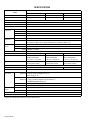
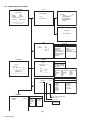
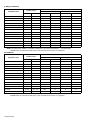
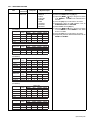
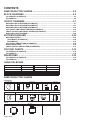
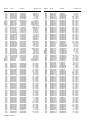
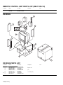
1
SERVICE MANUAL FLAT COLOUR TELEVISION 10 2006 YA476 AV-21MXP6/V, AV-25MXP6/V, AV-29MXP6/V BASIC CHASSIS CW3 [AV-21MXP6/V] [AV-25MXP6/V] [AV-29MXP6/V] TABLE OF CONTENTS 1 2 3 4 5 PRECAUTION. . . . . . . . . . . . . . . . . . . . . . . . . . . . . . . . . . . . . . . . . . . . . . . . . . . . . . . . . . . . . . . . . . . . . . . . . 1-3 SPECIFIC SERVICE INSTRUCTIONS . . . . . . . . . . . . . . . . . . . . . . . . . . . . . . . . . . . . . . . . . . . . . . . . . . . . . . 1-4 DISASSEMBLY . . . . . . . . . . . . . . . . . . . . . . . . . . . . . . . . . . . . . . . . . . . . . . . . . . . . . . . . . . . . . . . . . . . . . . . 1-6 ADJUSTMENT . . . . . . . . . . . . . . . . . . . . . . . . . . . . . . . . . . . . . . . . . . . . . . . . . . . . . . . . . . . . . . . . . . . . . . . 1-16 TROUBLESHOOTING . . . . . . . . . . . . . . . . . . . . . . . . . . . . . . . . . . . . . . . . . . . . . . . . . . . . . . . . . . . . . . . . . 1-42 COPYRIGHT © 2006 Victor Company of Japan, Limited No.YA476 2006/10 SPECIFICATION Contents Items AV-21MXP6/V AV-25MXP6/V AV-29MXP6/V Dimensions (W × H × D) 64.9 cm × 46.5 cm × 46.9 cm 72.8 cm × 53.6 cm × 47.6 cm 81.2 cm × 58.4 cm × 52.1 cm Mass 23.5 kg TV RF System B, G, I, D, K, M Colour System PAL / SECAM / NTSC 3.58 / NTSC 4.43 Stereo System PB STREO 32.0 kg Teletext System 43.0 kg --- Receiving Frequency VHF Low 46.25MHz - 140.25MHz (AS0 - S6) VHF High 147.25MHz - 423.25MHz (S7 - S36) UHF 431.25MHz - 863.25MHz (S37 - C57) CATV Mid (X - Z+2, S1 - S10) / Super (S11 - S20) / Hyper (S21 - S41) bands Intermediate Frequency VIF 38.0MHz (B, G, I, D, K, M) SIF 32.26 MHz (5.74 MHz: B), 32.15MHz (5.85 MHz: G), 31.45 MHz (6.55 MHz: I) 31.75 MHz (6.5 MHz: D), 32.15MHz (5.85 MHz: K), 33.5MHz (4.5MHz : M) Colour Sub Carrier PAL 4.43 MHz SECAM 4.40625 MHz / 4.25 MHz NTSC 3.58 MHz / 4.43 MHz Power Input AC110 V - AC240 V, 50 Hz/60 Hz (Operating Voltage 90V~260V) Power Consumption 105W (Max)/ 73W (Avg) 137W (Max)/ 91w (Avg) 170W (Max)/ 109w (Avg) Picture Tube Visible size : 52.1 cm, Measured diagonally H: 41.6 cm × V: 31.5 cm Visible size : 61.0 cm, Measured diagonally H: 48.6 cm × V: 36.8 cm Visible size : 69.0 cm, Measured diagonally H: 55.1 cm × V: 41.6 cm High Voltage 28.5 kV ±1.5 kV (at zero beam current) 30.5 kV ±1.5 kV (at zero beam current) 31.5 kV +1kV/-1.5kV (at zero beam current) Speaker 6.5 cm × 13 cm, oval type × 2 Audio Power Output 7 W + 7 W (Rated power output) Aerial Input 75 Ω unbalanced, coaxial Video / Audio Input-1/2/3 Component Video RCA pin jack × 3 [VIDEO-2] Y:1V(p-p), positive (negative sync), 75Ω Cb/Cr:0.7V(p-p), 75Ω S-Video Mini-DIN 4 pin × 1 [VIDEO-1] Y: 1V(p-p), positive (negative sync provided), 75Ω C: 0.286V(p-p) (Burst signal), 75Ω Video 1V(p-p), negative sync, 75Ω, RCA pin jack × 3 Audio 500mV(rms) (-4dBs), high impedance, RCA pin jack × 6 Video / Audio Output Video 1V(p-p), 75?, RCA pin jack × 1 Audio 500mV(rms)(-4dBs), Low impedance, RCA pin jack × 2 Headphone jack 3.5 mm stereo mini jack × 1 Remote Control Unit RM-C1285 (UM-3/AA/R6 dry cell battery × 2) Design and specifications subject to change without notice. 1-2 (No.YA476) 10 W + 10 W (Rated power output) SECTION 1 PRECAUTION 1.1 SAFETY PRECAUTIONS (1) The design of this product contains special hardware, many circuits and components specially for safety purposes. For continued protection, no changes should be made to the original design unless authorized in writing by the manufacturer. Replacement parts must be identical to those used in the original circuits. Service should be performed by qualified personnel only. (2) Alterations of the design or circuitry of the products should not be made. Any design alterations or additions will void the manufacturer's warranty and will further relieve the manufacturer of responsibility for personal injury or property damage resulting therefrom. (3) Many electrical and mechanical parts in the products have special safety-related characteristics. These characteristics are often not evident from visual inspection nor can the protection afforded by them necessarily be obtained by using replacement components rated for higher voltage, wattage, etc. Replacement parts which have these special safety characteristics are identified in the parts list of Service manual. Electrical components having such features are identified by shading on the schematics and by ( ) on the parts list in Service manual. The use of a substitute replacement which does not have the same safety characteristics as the recommended replacement part shown in the parts list of Service manual may cause shock, fire, or other hazards. (4) Don't short between the LIVE side ground and ISOLATED (NEUTRAL) side ground or EARTH side ground when repairing. Some model's power circuit is partly different in the GND. The difference of the GND is shown by the LIVE : ( ) side GND, the ISOLATED (NEUTRAL) : ( ) side GND and EARTH : ( ) side GND. Don't short between the LIVE side GND and ISOLATED (NEUTRAL) side GND or EARTH side GND and never measure the LIVE side GND and ISOLATED (NEUTRAL) side GND or EARTH side GND at the same time with a measuring apparatus (oscilloscope etc.). If above note will not be kept, a fuse or any parts will be broken. (5) If any repair has been made to the chassis, it is recommended that the B1 setting should be checked or adjusted (See B1 VOLTAGE). (6) The high voltage applied to the picture tube must conform with that specified in Service manual. Excessive high voltage can cause an increase in X-Ray emission, arcing and possible component damage, therefore operation under excessive high voltage conditions should be kept to a minimum, or should be prevented. If severe arcing occurs, remove the AC power immediately and determine the cause by visual inspection (incorrect installation, cracked or melted high voltage harness, poor soldering, etc.). To maintain the proper minimum level of soft X-Ray emission, components in the high voltage circuitry including the picture tube must be the exact replacements or alternatives approved by the manufacturer of the complete product. (7) Do not check high voltage by drawing an arc. Use a high voltage meter or a high voltage probe with a VTVM. Discharge the picture tube before attempting meter connection, by connecting a clip lead to the ground frame and connecting the other end of the lead through a 10kΩ 2W resistor to the anode button. (8) When service is required, observe the original lead dress. Extra precaution should be given to assure correct lead dress in the high voltage circuit area. Where a short circuit has occurred, those components that indicate evidence of overheating should be replaced. Always use the manufacturer's replacement components. (9) Isolation Check (Safety for Electrical Shock Hazard) After re-assembling the product, always perform an isolation check on the exposed metal parts of the cabinet (antenna terminals, video/audio input and output terminals, Control knobs, metal cabinet, screw heads, earphone jack, control shafts, etc.) to be sure the product is safe to operate without danger of electrical shock. a) Dielectric Strength Test The isolation between the AC primary circuit and all metal parts exposed to the user, particularly any exposed metal part having a return path to the chassis should withstand a voltage of 3000V AC (r.m.s.) for a period of one second. (. . . . Withstand a voltage of 1100V AC (r.m.s.) to an appliance rated up to 120V, and 3000V AC (r.m.s.) to an appliance rated 200V or more, for a period of one second.) This method of test requires a test equipment not generally found in the service trade. b) Leakage Current Check Plug the AC line cord directly into the AC outlet (do not use a line isolation transformer during this check.). Using a "Leakage Current Tester", measure the leakage current from each exposed metal part of the cabinet, particularly any exposed metal part having a return path to the chassis, to a known good earth ground (water pipe, etc.). Any leakage current must not exceed 0.5mA AC (r.m.s.). However, in tropical area, this must not exceed 0.2mA AC (r.m.s.). Alternate Check Method Plug the AC line cord directly into the AC outlet (do not use a line isolation transformer during this check.). Use an AC voltmeter having 1000Ω per volt or more sensitivity in the following manner. Connect a 1500Ω 10W resistor paralleled by a 0.15µF AC-type capacitor between an exposed metal part and a known good earth ground (water pipe, etc.). Measure the AC voltage across the resistor with the AC voltmeter. Move the resistor connection to each exposed metal part, particularly any exposed metal part having a return path to the chassis, and measure the AC voltage across the resistor. Now, reverse the plug in the AC outlet and repeat each measurement. Any voltage measured must not exceed 0.75V AC (r.m.s.). This corresponds to 0.5mA AC (r.m.s.). However, in tropical area, this must not exceed 0.3V AC (r.m.s.). This corresponds to 0.2mA AC (r.m.s.). AC VOLTMETER (HAVING 1000 /V, OR MORE SENSITIVITY) 0.15 F AC-TYPE 1500 10W PLACE THIS PROBE ON EACH EXPOSED METAL PART GOOD EARTH GROUND (No.YA476)1-3 SECTION 2 SPECIFIC SERVICE INSTRUCTIONS 2.1 FEATURES DVD PICTURE MODE This function can enhance the picture quality of DVD. The screen can be made sharp or soft by this setting. AUTO SIGNAL DETECT When input DVD signal to VIDEO-2, detect the input signal and change the input mode to VIDEO-2 automatically. CINEMA SURROUND This function can enjoy an enhanced sound for wider audience. PICTURE MODE This function can adjust the picture settings automatically. There are BRIGHT, STANDARD and SOFT in the PICTURE MODE. 2.2 RETURN + This function can set a channel frequently view to the Return Channel and you can view that channel at any time with onetouch. AI ECO SENSOR This function can adjust TV screen contrast according to the brightness of your room. MaxxBass MaxxBass enhances bass sound that cannot be reproduced by normal speakers to be heard by our ears. MAIN DIFFERENCE LIST Item MAIN PWB 1-4 (No.YA476) AV-21MXP6/V AV-25MXP6/V AV-29MXP6/V SCW-1645A-H2 SCW-1646-H2 SCW-1647A-H2 2.3 TECHNINAL INFORMATION 2.3.1 MAIN MI-COM (CPU) PIN FUNCTION Pin No. 1 2 3 4 5 6 7 8 9 10 11 12 13 14 15 16 17 18 19 20 21 22 23 24 25 26 27 28 29 30 31 32 33 34 35 36 37 38 39 40 41 42 43 44 45 46 47 48 49 50 51 52 53 54 55 56 57 58 59 60 61 62 63 64 Pin name I/O VssP2 VssC4 V1.8C4 V3.3A3 VrefP_Sdac VrefN_Sdac VrefP_Sdac VrefN_Sdac VrefP_Sdac XtalIn XtalOut VssA1 NECK CONT V5P1 Ph2 Ph1 Gnd1 SecPll Dec8G EW VDRBVDRA+ Vif1 Vif2 Vsc Iref GndIF Sif1 Sif2 AGC EHT Ssif/RefIn/Avl/ RefOut I I I I I I O I I I O O O I I I I I O I O L3 R3 L-OUT R-OUT DecsDem QssO/AmO/ AudeEm Gnd2 PllIf SifAgc IfVo/FmRo/DvbO NC V8AudioSwitches AgcSsif V5P2 V-OUT L1 R1 V3 C4 Audio2InL Audio2InR V2/Y L2 R2 Y3/Cvbs C1 AudioLsL AudioLsR HP-L HP-R CVBSO/PIP I I O O O O O I I O I I I I I I I I I I I O O O O O Pin No. GND 65 GND 66 1.8V (Digital) 67 3.3V 68 3.3V (Positive) 69 GND 70 3.3V (Negative) 71 GND 72 3.3V (Positive) 73 24.576MHz for system clock 74 24.576MHz for system clock 75 GND 76 V-guard input/ I/O switch 77 1.8V regulator control 78 +5V 79 Phase-2 filter 80 Phase-1 filter 81 GND 82 SECAM PLL decoupling 83 Bandgap decoupling 84 East-West drive output 85 Vertical drive B output 86 Vertical drive A output 87 Video IF input 1 88 Video IF input 2 89 Vertical sawtooth capacitor 90 Reference current input 91 GND 92 Sound IF input 1 93 Sound IF input 2 94 Tuner AGC output 95 EHT/overvoltage protection input 96 Automatic Volume Levelling/ sound IF input / subcar- 97 rier reference output / external reference signal input for I signalmixer for DVB operation Audio-L3 input (left signal) 98 Audio-R3 input (right signal) 99 Audio L output 100 Audio R output 101 Decoupling sound demodulator 102 QSS intercarrier output / AM output / deemphasis / 103 (front-end audio out) GND 104 IF-PLL loop filter 105 AGC sound IF 106 Not used 107 Not used 108 8V 109 AGC capacitor second sound IF 110 5V 111 Video output 112 Audio-L1 input 113 Audio-R1 input 114 Video V3 input 115 Not used 116 Not used 117 Not used 118 Video V2 input 119 Audio L2 input (Left signal) 120 Audio R2 input (right signal) 121 S-Video Y1 input 122 S-Video C1 input 123 Audio L output for audio power amplifier 124 Audio R output for audio power amplifier 125 Not used 126 Not used 127 CVBS / PIP output 128 Function Pin name I/O SVM FbiSo Hout VssComb V5Comb Vin/R2/Pr Uin/B2/Pb Yin/G2/Y Ysync Yout Uout/INSSW2 NC INSSW3 R3/Pr G3/Y B3/Pb Gnd3 V5P3 BCL BLKIN Rout Gout Bout V3.3A1 RefAdN V3.3RefAdP RefAd GndA V1.8A V3.3A2 VssADC V1.8ADC REMOTE O I O I I I I I O I O I I I I I I I O O O I I I I I I I Not used Flyback input/sandcastle output Horizontal output GND 5V PIP R input PIP B input PIP G input Not used Not used YUV insertion input Not used YUV insertion input Component PR input (Video-2) Component Y input (Video-2) Component PB input (Video-2) GND 5V Beam current limiter input Black current input R output G output B output 3.3V GND 3.3V (Positive) 3.3/2V GND 1.8V 3.3V GND 1.8V Remote control PW_LED PW_LED V1.8C2 VssC2 TIMER TIMER I I I - POWER LED control POWER LED control 1.8V GND Not used Not used VER_PROTECT S_REDUCE P00/I2SDI1 POWER SCL1 SDA1 V3.3P ROTATION 3.58/OTHER A_MUTE 4.5/OTHER PROT ECO_IN V1.8C1 DecV1V8 KEY_IN VDO-DET VSSC1+P1 S_V_DET P25/PWM4 V1.8C3 VssC3 P12/Int2 SDA0 SCL0 O O O O I I/O I O O O O I I I I I I I O I I I/O I Function X-ray protect Sound control Not used SUB POWER control I2C bus clock I2C bus data 3.3V Rotation NTSC 3.58 detection Audio muting NTSC 4.43 detection Protect ECO sensor level detection 1.8V (Digital) 1.8V Key scan data Video DET input Digital GND S-Video DET input GTVA_reset 1.8V (Digital) GND External interrupt I2C bus data (for memory) I2C bus clock (for memory) (No.YA476)1-5 SECTION 3 DISASSEMBLY 3.1 DISASSEMBLY PROCEDURE [AV-21MXP6/V] 3.1.1 REMOVING THE REAR COVER • Unplug the power cord. (1) Remove the 2 screws [A], 7 screws [B] and 4 screws [C] as shown in Fig.1. (2) Withdraw the REAR COVER toward you. CAUTION: When reinstalling the rear cover, carefully push it inward after inserting the MAIN PWB into the REAR COVER groove. 3.1.2 REMOVING THE MAIN PW BOARD • Remove the REAR COVER. (1) Slightly raise the both sides of the MAIN PWB (with BASS PWB connected) by hand. (2) Withdraw the MAIN PWB backward. (If necessary, take off the wire clamp and connectors, etc.) 3.1.3 REMOVING THE SPEAKER • Remove the REAR COVER. (1) Remove the 2 screws [D] as shown in Fig.1. (2) Follow the same steps when removing the other hand SPEAKER. 3.1.4 CHECKING THE MAIN PW BOARD • To check the back side of the MAIN PWB. (1) Pull out the MAIN PWB. (Refer to REMOVING THE MAIN PW BOARD). (2) Erect the MAIN PWB vertically so that you can easily check its back side. CAUTIONS: • Before turning on power, make sure that the CRT earth wire and other connectors are properly connected. • When repairing, connect the DEG. COIL to the DEG. connector on the MAIN PWB. 3.1.5 WIRE CLAMPING AND CABLE TYING (1) Be sure to clamp the wire. (2) Never remove the cable tie used for tying the wires together. Should it be inadvertently removed, be sure to tie the wires with a new cable tie. 1-6 (No.YA476) [AV-21MXP6/X] FRONT CABINET D SPEAKER CRT SOCKET PWB (Within MAIN PWB) FRONT COTROL PWB (Within MAIN PWB) D SPEAKER MAIN PWB POWER CORD BASS PWB REAR COVER B A C Fig.1 (No.YA476)1-7 3.2 DISASSEMBLY PROCEDURE [AV-25MXP6/V] 3.2.1 REMOVING THE REAR COVER • Unplug the power cord. (1) Remove the 11 screws [A] and 4 screws [B] as shown in Fig.2. (2) Withdraw the REAR COVER toward you. CAUTION: When reinstalling the rear cover, carefully push it inward after inserting the MAIN PWB into the REAR COVER groove. 3.2.2 REMOVING THE MAIN PW BOARD • Remove the REAR COVER. (1) Slightly raise the both sides of the MAIN PWB (with BASS PWB connected) by hand. (2) Withdraw the MAIN PWB backward. (If necessary, take off the wire clamp and connectors, etc.) 3.2.3 REMOVING THE SPEAKER • Remove the REAR COVER. (1) Remove the 2 screws [C] as shown in Fig.2. (2) Follow the same steps when removing the other hand SPEAKER. 3.2.4 CHECKING THE MAIN PW BOARD • To check the back side of the MAIN PWB. (1) Pull out the MAIN PWB. (Refer to REMOVING THE MAIN PW BOARD). (2) Erect the MAIN PWB vertically so that you can easily check its back side. CAUTIONS: • Before turning on power, make sure that the CRT earth wire and other connectors are properly connected. • When repairing, connect the DEG. COIL to the DEG. connector on the MAIN PWB. 3.2.5 WIRE CLAMPING AND CABLE TYING (1) Be sure to clamp the wire. (2) Never remove the cable tie used for tying the wires together. Should it be inadvertently removed, be sure to tie the wires with a new cable tie. 1-8 (No.YA476) [AV-25MXP6/V] FRONT CABINET C SPEAKER CRT SOCKET PWB (Within MAIN PWB) FRONT COTROL PWB (Within MAIN PWB) SPEAKER C POWER CORD MAIN PWB BASS PWB REAR COVER A B Fig.2 (No.YA476)1-9 3.3 DISASSEMBLY PROCEDURE [AV-29MXP6/V] 3.3.1 REMOVING THE REAR COVER • Unplug the power cord. (1) Remove the 16 screws [A] as shown in Fig.3. (2) Withdraw the REAR COVER toward you. CAUTION: When reinstalling the rear cover, carefully push it inward after inserting the MAIN PWB into the REAR COVER groove. 3.3.2 REMOVING THE CHASSIS (CHASSIS BASE AND CONTROL BASE) • Remove the REAR COVER. (1) Slightly raise the both sides of the CHASSIS by hand and remove the 2 claws [B] under the CHASSIS from the front cabinet as shown in Fig.3. (2) Withdraw the CHASSIS backward. (If necessary, take off the wire clamp, connectors etc.) NOTE: When conducting a check with power supplied, be sure to confirm that the CRT earth wire is connected to the CRT SOCKET PWB and the MAIN PWB. 3.3.3 REMOVING THE AV TERMINAL BOARD • Remove the REAR COVER. (1) Remove the 4 screws [C] as shown in Fig.3. (2) When you pull out the AV TERMINAL BOARD in the direction of arrow [D] as shown in Fig.3, it can be removed. 3.3.4 REMOVING THE CONTROL BASE • Remove the REAR COVER. • Remove the CHASSIS. (1) While pushing down the 2 claws [E] as shown in Fig. 4 and pull out the CONTROL BASE in the direction of arrow [F] as shown in Fig. 4, the control base can be removed. (If necessary, take off the wire, connectors etc.) 1-10 (No.YA476) 3.3.5 REMOVING THE SPEAKER • Remove the REAR COVER. (1) Remove the 2 screws [G] as shown in Fig.3. (2) Withdraw the SPEAKER backward. (3) Follow the same steps when removing the other hand SPEAKER. 3.3.6 CHECKING THE MAIN PW BOARD • To check the back side of the MAIN PWB. (1) Pull out the CHASSIS and CONTROL BASE. (Refer to the procedure described in REMOVING THE CHASSIS) (2) Put the CHASSIS in upright position with the MAIN PWB's solderside faced to the right. The FBT must be positioned on top. (Viewed from the rear) (3) Put the CONTROL PWBs in an appropriate position, taking care not giving tension to the ribbon cables that connect to the MAIN PWB. CAUTIONS: • Use insulating materials, if necessary, to avoid possible electrical contacts between PWBs and expose terminals, etc. • Before turning on power, make sure that the CRT earth wire and other connectors are properly connected. • When repairing, connect the DEG. COIL to the DEG. connector on the MAIN PWB. 3.3.7 WIRE CLAMPING AND CABLE TYING (1) Be sure to clamp the wire. (2) Never remove the cable tie used for tying the wires together. Should it be inadvertently removed, be sure to tie the wires with a new cable tie. [AV-29MXP6/V] [FRONT SIDE] CONTROL BASE FRONT CABINET E F CHASSIS BASE Fig.4 CRT SOCKET PWB G SPEAKER FRONT CONTROL PWB CLAW B (under side) G MAIN PWB Fig.4 SPEAKER AV TERMINAL BOARD CONTROL BASE CLAW B (under side) D BASS PWB CHASSIS BASE C POWER CORD REAR COVER A Fig.3 (No.YA476)1-11 3.4 MEMORY IC REPLACEMENT • This model uses the memory IC. Memory IC: IC702 on MAIN PWB The memory IC memorizes data for correctly operating the video and deflection circuits. When replacing the memory IC, be sure to use the same type IC written with the initial values of data. In other words, use the specific IC listed in "PRINTED WIRING BOARD PARTS LIST". For its mounting location, refer to "ADJUSTMENT LOCATIONS". 3.4.1 MEMORY IC REPLACEMENT PROCEDURE 1. Power off Switch off the power and disconnect the power plug from the AC outlet. 2. Replace the memory IC Be sure to use the memory IC written with the initial setting values. 3. Power on Connect the power plug to the AC outlet and switch on the power. 4. System constant check and setting * It must not adjust without signal. (1) Press the [DISPLAY] key and the [PICTURE MODE] key of the REMOTE CONTROL UNIT simultaneously. (2) The SERVICE MODE screen of Fig. 1 will be displayed. (3) While the SERVICE MODE is displayed, press the [DISPLAY] key and the [PICTURE MODE] key simultaneously, and the SYSTEM CONSTANT SET screen of Fig. 2 will be displayed. (4) Check the setting values of the SYSTEM CONSTANT SET. If the value is different, select the setting item with the [MENU /] key, and set the correct value with the [MENU /] key. (5) Press the [OK] key to memorize the setting value. (6) Press the [DISPLAY] key twice, and return to the normal screen. 5. Receiving channel setting Refer to the OPERATING INSTRUCTIONS and set the receive channels (Channels Preset) as described. 6. User settings Check the user setting items according to the given in page later. Where these do not agree, refer to the OPERATING INSTRUCTIONS and set the items as described. 7. SERVICE MODE setting Verify what to set in the SERVICE MODE, and set whatever is necessary (Fig.1). Refer to the SERVICE ADJUSTMENT for setting. SERVICE MENU SERVICE MENU 1. IF 2. V/C 3. AUDIO 4. DEF 5. VSM W/B 6. S TATUS 7. PLUG & PLAY (ON) 1-7 : SELECT DISPLAY : EXIT ******* **** ***** ***** **** **** *** *** Fig.1 SYSTEM CONSTANT-1 SYSTEM CONSTANT SET 1 : MULTI :NO :NO :NO :NO :EV SYSTEM COMB TILT SUPER BASS TEXT LANGUAGE : SEL : OPE DISP : EXIT SYSTEM CONSTANT-2 SYSTEM CONSTANT SET 2 SOUND BILINGUAL BLUE BACK MUTE COLOUR AUTO ECO SENSOR INTER CARRIER : SEL : OPE :PB :NO :NO :NO :ECO :NO DISP : EXIT SYSTEM CONSTANT-3 KEY ASSIGNMENT OF REMOTE CONTROL UNIT SYSTEM CONSTANT SET 3 DISPLAY key MENU key key MENU key OK key MENU key MENU EXIT SURROUND PICTURE BOOSTER COMPONENT PIP S INPUT MAXX BASS : SEL : OPE PICTURE MODE key Fig.2 1-12 (No.YA476) :YES :NO :YES :YES :YES :YES DISP : EXIT 3.4.2 SYSTEM CONSTANT SETTING Setting value Setting item AV-21MXP6/V AV-25MXP6/V AV-29MXP6/V MULTI ← ← COMB NO ← YES TILT NO ← YES SUPER BASS NO ← ← TEXT NO ← ← LANGUAGE E/V ← ← SOUND PB ← ← BILINGUAL NO ← ← BLUE BACK MUTE NO ← ← COLOUR AUTO NO ← ← SYSTEM ECO ← ← INTER CARRIER NO ← ← SURROUND YES ← ← PICTURE BOOSTER NO ← ← COMPONENT YES ← ← PIP YES ← ← S INPUT YES ← ← MAXX BASS YES ← ← ECO SENSOR 3.4.3 SETTINGS OF FACTORY SHIPMENT 3.4.3.3 3.4.3.1 (1) PICTURE SETTING BUTTON OPERATION Setting item Setting position REMOTE CONTROL MENU OPERATION Setting item Setting position POWER Off PICTURE MODE CHANNEL PR 1 VOLUME 15 CONTRAST / BRIGHT / SHARP Centre / COLOUR / TINT 3.4.3.2 REMOTE CONTROL DIRECT OPERATION Setting item Setting position CHANNEL PR1 VOLUME 15 PICTURE MODE BRIGHT DISPLAY Indicated TV/VIDEO TV CINEMA SURROUND OFF BRIGHT WHITE BALANCE COOL VNR AUTO (2) SOUND SETTING Setting item Setting position STEREO l/ll STEREO SOUND AI VOLUME OFF SOUND MODE MUSIC BALANCE Centre CINEMA SURROUND OFF MAXX BASS OFF (No.YA476)1-13 (3) FEATURE SETTING 3.4.4 SERVICE MODE SETTING ITEMS Setting item Setting position DVD MENU AUTO SIGNAL DETECT ON DVD PICTURE MODE OFF DVD THEATER STATUS OFF DVD SOUND MODE THEATER ON TIMER OFF OFF TIMER OFF CHILD LOCK OFF COMPRESS (16:9) OFF AI ECO SENSOR OFF (4) INSTALL SETTING Setting item Setting position AUTO PROGRAM TV channel automatically set EDIT/MANUAL PRESET CH only COLOUR SYSTEM PAL LANGUAGE VIETNAM VIDEO-2 SETTING COMPONENT BLUE BACK ON BEEP ON Setting item Setting value 1. IF 1. VCO 2. DELAY POINT 2. V / C 1.SCREEN (READ DATA) 2.CUTOFF / CUT OFF THEATER (B/G) 3.WDR (R/G/B) 4.BRIGHT (TV/VDO 1/2/3) 5.CONT. (TV/VDO 1/2/3) 6.COLOUR (TV/VDO 1/2/3) 7.TINT (TV/VDO 1/2/3 /THEATER) 8.SHARP (TV/VDO 1/2/3) 9.Y DELAY (TV/VDO 1/2/3/S-VDO) 10.TINT DVD (TV/VDO/THEATER) 11.AMP T.SHARP (TV/VDO) 3. AUDIO [Do not adjust] 1. DCXO ADJ 2. NICAM lower ERRLIM 3. NICAM upper ERRLIM 4. A2 ID THR 5. MENU EQUALIZER 4. DEF 1. V-SHIFT 2. V-SLOPE 3. V-SIZE 4. H-CENT 5. H-SIZE 6. TRAPEZ 7. EW-PIN 8. COR-UP 9. COR-LO 10. ANGLE 11. BOW 12. V-S.CR 13. V-LIN 14. V-ZOOM 5. VSM PRESET 1. BRIGHT 2. CONT 3. COLOUR 4. SHARP 5. HUE 1. R DRIVE 2. G DRIVE 3. B DRIVE 1-14 (No.YA476) 6. STATUS [Dispaly only] --- 7. PLUG & PLAY(ON) [Dispaly only] --- 3.5 REPLACEMENT OF CHIP COMPONENT 3.5.1 CAUTIONS (1) Avoid heating for more than 3 seconds. (2) Do not rub the electrodes and the resist parts of the pattern. (3) When removing a chip part, melt the solder adequately. (4) Do not reuse a chip part after removing it. 3.5.2 SOLDERING IRON (1) Use a high insulation soldering iron with a thin pointed end of it. (2) A 30w soldering iron is recommended for easily removing parts. 3.5.3 REPLACEMENT STEPS 1. How to remove Chip parts 2. How to install Chip parts [Resistors, capacitors, etc.] [Resistors, capacitors, etc.] (1) As shown in the figure, push the part with tweezers and alternately melt the solder at each end. (1) Apply solder to the pattern as indicated in the figure. (2) Grasp the chip part with tweezers and place it on the solder. Then heat and melt the solder at both ends of the chip part. (2) Shift with the tweezers and remove the chip part. [Transistors, diodes, variable resistors, etc.] [Transistors, diodes, variable resistors, etc.] (1) Apply extra solder to each lead. SOLDER (1) Apply solder to the pattern as indicated in the figure. (2) Grasp the chip part with tweezers and place it on the solder. (3) First solder lead A as indicated in the figure. SOLDER A (2) As shown in the figure, push the part with tweezers and alternately melt the solder at each lead. Shift and remove the chip part. B C (4) Then solder leads B and C. A B NOTE : After removing the part, remove remaining solder from the pattern. C (No.YA476)1-15 SECTION 4 ADJUSTMENT 4.1 ADJUSTMENT PREPARATION 4.3 (1) There are 2 ways of adjusting this TV : One is with the REMOTE CONTROL UNIT and the other is the conventional method using adjustment parts and components. (2) The adjustment using the REMOTE CONTROL UNIT is made on the basis of the initial setting values. The setting values which adjust the screen to the optimum condition can be different from the initial setting values. (3) Make sure that connection is correctly made AC to AC power source. (4) Turn on the power of the TV and measuring instruments for warming up for at least 30 minutes before starting adjustments. (5) If the receive or input signal is not specified, use the most appropriate signal for adjustment. (6) Never touch the parts (such as variable resistors, transformers and condensers) not shown in the adjustment items of this service adjustment. 4.2 PRESET SETTING BEFORE ADJUSTMENT Unless otherwise specified in the adjustment items, preset the following functions with the REMOTE CONTROL UNIT. Item Preset value PICTURE MODE(VSM) BRIGHT VNR OFF AI ECO SENSOR OFF BALANCE Centre BASS / TREBLE / BALANCE Centre CINEMA SURROUND OFF MEASURING INSTRUMENT AND FIXTURES (1) (2) (3) (4) DC voltmeter (or digital voltmeter) Oscilloscope HV voltmeter Signal generator (Pattern generator : PAL/NTSC) (5) Remote control unit 4.4 ADJUSTMENT ITEMS CHECK ITEMS • B1 VOLTAGE check • HIGH VOLTAGE check • IF VCO check TUNER / IF CIRCUIT • DELAY POINT (AGC) adjustment FOCUS • FOCUS adjustment DEFLECTION CIRCUIT • V.SLOPE adjustment • V.POSITION adjustment • V.SIZE adjustment • H.POSITION adjustment • H.SIZE adjustment [Except AV-21MXP6/V] • SIDE PIN adjustment [Except AV-21MXP6/V] • TRAPEZIUM adjustment [Except AV-21MXP6/V] • V. LINEARITY adjustment • CORNER adjustment [Except AV-21MXP6/V] • H. PARALLEL adjustment • H.BOW adjustment VIDEO CIRCUIT • WHITE BALANCE adjustment • SUB BRIGHT adjustment • SUB CONTRAST adjustment • SUB COLOUR adjustment • SUB TINT adjustment VSM PRESET SETTING • VSM PRESET PURITY AND CONVERGENCE • PURITY adjustment • STATIC CONVERGENCE adjustment • DYNAMIC CONVERGENCE adjustment 1-16 (No.YA476) 4.5 ADJUSTMENT LOCATION [AV-21MXP6/V, AV-25MXP6/V] FRONT MAIN PWB ASS'Y (FRONT LED) CN10A S804 S802 S805 S803 S801 J808 J807 J806 J809 POWER SW CN00A 4 S901 POWER CORD 1 FRONT CN00S PW IC702 1 T DEG COIL DEG 6 IC701 DEF YOKE 12 HV 4 1 U 1 HVT BASS PWB ASS'Y 4 1 GND B1 J801 J802 J803 J804 3 CN00C MAIN PWB ASS'Y 6 TU001 2 IC 1 CN00C 1. 5V 2. SCL0 3. SDA0 4. SCL1 5. SDA1 6. GND 1 CN00B CN00B 1. B1 2. NC 3. GND UPPER : FOCUS LOWER : SCREEN MAIN PWB ASS'Y (CRT SOCKET) (SOLDER SIDE) 1 TOP T 6 TP-47G/R TP-47B E1 TP-47R/G U TP-E 4 1 CRT EARTH (BRAIDED ASS'Y) (No.YA476)1-17 4.6 ADJUSTMENT LOCATION [AV-29MXP6/V] FRONT CONTROL PWB ASS’Y (1/2) FRONT CONTROL PWB ASS’Y (2/2) SPEAKER (R) SPEAKER (L) FRONT S805 S801 S803 S804 S806 S802 S901 W J804 J803 J802 J801 FRONT CN00S CNDEG CN002 CN001 PW POWER CORD DEG COIL ROTATION COIL MAIN PWB ASS’Y FRONT R CN002 CN001 CN00W IC702 T 1 8 IC701 12 DEF YOKE HV 6 CN00C 1. 5V 2. SCL0 3. SDA0 4. SCL1 5. SDA1 6. GND 1 BASS PWB ASS'Y GND 6 1 1 HVT U B1 5V J805 J801 J802 J803 J804 6 1 5 1 CN00X 1. B1 2. NC 3. X-RAY2 4. X-RAY1 5. GND GND TU001 UPPER : FOCUS LOWER : SCREEN MAIN PWB ASS’Y (CRT SOCKET) (SOLDER SIDE) TOP TP-E TP-47B TP-47R TP-47G T 1 CRT EARTH (BRAIDED ASS'Y) 8 E1 E2 CRT EARTH (BRAIDED ASS'Y) 1-18 (No.YA476) 1 U 6 4.7 BASIC OPERATION OF SERVICE MODE 4.7.1 TOOL OF SERVICE MODE OPERATION Operate the SERVICE MODE with the REMOTE CONTROL UNIT. 4.7.2 SERVICE MODE ITEMS With the SERVICE MODE, various adjustments can be made, and they are broadly classified in the following items of settings. 1.IF This mode adjusts the setting values of the IF circuit. 2. V/C This mode adjusts the setting values of the VIDEO circuit. 3.AUDIO This mode adjusts the setting values of the multiplicity AUDIO circuit. [Do not adjust] 4. DEF This mode adjusts the setting values of the DEFLECTION circuit for each aspect mode given below. 5.VSM PRESET This mode adjusts the initial setting values of BRIGHT, STANDARD and SOFT. (VSM : Video Status Memory) 6.STATUS It is no requirement to adjustment. [Do not adjust] 7.PLUG & PLAY (ON) This mode adjusts the setting values of the PIP circuit. [Do not adjust] 4.7.3 BASIC OPERATION IN SERVICE MODE 4.7.3.1 HOW TO ENTER THE SERVICE MODE (1) Press the [DISPLAY] key and the [PICTURE MODE] key simultaneously, then enter the SERVICE MODE. (2) When the main menu is displayed, press any key of the [7] to [9] key to enter the corresponding sub menu mode. SERVICE MENU SERVICE MENU 1. IF 2. V/C 3. AUDIO 4. DEF 5. VSM W/B 6. S TATUS 7. PLUG & PLAY (ON) 1-7 : SELECT DISPLAY : EXIT Fig.1 SERVICE MODE SELECT KEY DISPLAY key MENU key key MENU key OK key MENU key EXIT PICTURE MODE key SETTING METHOD 1.IF [1. VCO] : It must not adjust without signal (1) [1] key Select 1.IF. (2) [1] key Select 1.VCO(CW). Check the arrow position between the ABOVE REF. and BELOW REF. (3) [DISPLAY] key Return to the SERVICE MODE main manu screen. 2. V/C, 4. DEF (1) [2], [4] key Select one from 2. V/C, 4. DEF. (2) [MENU /] key Select setting items. (3) [MENU /] key Set the setting values of the setting items. ******* **** ***** ***** **** **** *** *** MENU 4.7.3.2 5.VSM W/B (1) [5] key Select 5.VSM W/B. (2) [OK] key Select setting items. (3) [MENU /] key Set the setting values of the setting items. 4.7.3.3 MEMORIZE THE ADJUSTMENT DATA When Mnt is completed, press the [OK] key to memorize the adjustment value. If not to do so, the data is not memorized to the memory IC. And if exit the adjustment mode before to memorize the data, the adjustment value which you have changed will be canceled. Fig.2 4.7.3.4 RELEASE OF SERVICE MODE After completing the setting, return to the SERVICE MODE, then again press the [DISPLAY] key. (No.YA476)1-19 4.7.4 SERVICE MODE FLOW CHART 1. IF SERVICE MENU SERVICE MENU IF SERVICE MENU 1. IF 2. V/C 3. AUDIO 4. DEF 5. VSM W/B 6. STATUS 7. PLUG & PLAY (ON) 1-7 : SELECT VCO (CW) TOO HIGH ABOVE REFERENCE JUST REFERENCE BELOW REFERENCE TOO LOW *****MHz 1. VCO 2. DELAY POINT DISPLAY : EXIT ******* **** ***** ***** **** **** *** *** DELAY POINT AGC TAKEOVER ** 2. V/C Setting item V/C PAL 1. SCREEN HBC WBC BRI 6. STATUS 1.SCREEN (READ DATA) 2.CUTOFF / CUT OFF THEATER (B/G) 3.WDR (R/G/B) 4.BRIGHT (TV/VDO 1/2/3) 5.CONT. (TV/VDO 1/2/3) 6.COLOUR (TV/VDO 1/2/3) 7.TINT (TV/VDO 1/2/3 / THEATER) ** ** ** 8.SHARP (TV/VDO 1/2/3) 9.Y DELAY (TV/VDO 1/2/3/ S-VDO) 10.TINT DVD (TV/VDO/ THEATER) 11.AMP T.SHARP (TV/VDO) 3. AUDIO Setting item AUDIO 1. DCXO ADJ. = NOT NICAM STATUS V/C STATUS ECO EOF ** ** NOL 1. DCXO ADJ 2. NICAM lower ERRLIM 3. NICAM upper ERRLIM 4. A2 ID THR *** VNR ** ***** ADC ECO = ** 0002 0009 COSMIC STATUS 000A ** ** ** ** ** ** ** ** MENU EQUALIZER ******* ******* ******* EQUALIZER RF EQUALIZER VIDEO EQUALIZER DVD USER SOUND TURBO THEATER MUSIC NEWS USER SOUND TURBO THEATER MUSIC NEWS USER DRAMA THEATER MUSIC 4. DEF 4 : 3 / 16 : 9 DEF FULL 1. V-SHIFT Setting item 50Hz *** ( ) ** 1. V-SHIFT 2. V-SLOPE 3. V-SIZE 4. H-CENT 5. H-SIZE 6. TRAPEZ 7. EW-PIN 8. COR-UP 5. VSM W/B Setting value (Hexadecimal) Setting item VSM PRESET 1. BRIGHT BRIGHT *** 1. BRIGHT 2. CONT 3. COLOUR 4. SHARP 5.HUE Setting value 1. R-DRIVE 2. G-DRIVE 3. B-DRIVE Sereen size FULL COMPRESS Fig.3 1-20 (No.YA476) 9. COR-LO 10. ANGLE 11. BOW 12. V-S. CR 13. V-LIN 14. V-ZOOM 4.8 INITIAL SETTING VALUE OF SERVICE MODE (1) Adjustment of the SERVICE MODE is made on the basis of the initial setting values:however, the new setting values which set the screen in its optimum condition may differ from the initial setting value. (2) Do not change the initial setting values of the setting items not listed in "ADJUSTMENT PROCEDURE". (3) The " --- " means adjustment is not possible. (4) " 12.TWIN CONT " is displayed only in the models with PIP function. [2. V/C] * is variable values for adjustment. [AV-21MXP6/V] Adjustment item Variable range Initial setting value PAL 1. SCREEN BRI 2. CUT OFF B CUT OFF THEATER 3. WDR 4. BRIGHT 5. CONT. 0 ~ 63 31* 31* 31* 31* --- 31* 31* 0 ~ 63(-32 ~ +31) 43* 43* 43* 43* --- +0* +0* G 0 ~ 63(-32 ~ +31) 28* 28* 28* 28* --- -3* -3* B 0 ~ 63(-32 ~ +31) --- --- --- --- -11 -7 -7 G 0 ~ 63(-32 ~ +31) --- --- --- --- -5 -2 -2 R 0 ~ 63(-32 ~ +31) 35* 35* 35* 35* --- 0 0 G 0 ~ 63(-32 ~ +31) 32 32 32 32 --- 0 0 B 0 ~ 63(-32 ~ +31) 40* 40* 40* 40* --- 0 0 0 ~ 63 34* 34* 34* 34* --- --- --- VIDEO-1(COMPOSITE/S) (-32 ~ +31) -1 -1 -1 -1 --- --- --- VIDEO-2(COMPONENT) (-32 ~ +31) -1 -1 -1 -1 --- +2 +2 VIDEO-3(COMPOSITE) (-32 ~ +31) -1 -1 -1 -1 --- --- --- 0 ~ 63 18* 18* 18* 18* --- --- --- (-32 ~ +31) +2 +2 +2 +2 --- +1 +1 RF RF VIDEO 6. COLOUR 7. TINT 8. SHARP 9. Y DELAY 10. TINT DVD SECAM NTSC3. NTSC4. VIDEO COMPONENT(V-2) 58 43 2 525i 625i 0 ~ 63(-32 ~ +31) 42* 29* 31* +1 --- --- --- VIDEO-1(COMPOSITE/S) RF (-32 ~ +31) +0 +0 +2 +0 --- --- --- VIDEO-2(COMPONENT) (-32 ~ +31) +0 +0 +2 +0 --- +4 +5 VIDEO-3(COMPOSITE) (-32 ~ +31) +0 +0 +2 +0 --- --- --- 0 ~ 63(-32 ~ +31) --- --- 32* +4 --- --- --- VIDEO RF (-32 ~ +31) --- --- +4 +2 --- --- --- THEATER (-32 ~ +31) --- --- +4 +3 --- --- --- RF 0 ~ 63 53 53 53 53 --- 40 40 VIDEO 0 ~ 63 55 55 55 55 --- 40 40 RF 0 ~ 15 7 7 5 5 --- --- --- VIDEO 0 ~ 15 6 9 7 7 --- --- --- S-VIDEO 0 ~ 15 7 9 9 9 --- --- --- 0 ~ 63(-32 ~ +31) 37* -1 +0 +0 --- +3 +1 VIDEO RF (-32 ~ +31) +1 -2 +0 +0 --- +3 +1 THEATER (-32 ~ +31) -1 -1 --- --- --- +0 +1 11. AMP T.SHARP RF VIDEO 0 ~ 63 0 0 0 0 --- 0 0 12. TWIN CONT. TWIN (RF) --- --- --- --- --- --- --- --- --- --- --- --- --- --- --- --- TWIN (VIDEO) (No.YA476)1-21 [AV-25MXP6/V] Adjustment item Variable range Initial setting value PAL 1. SCREEN 2. CUT OFF CUT OFF THEATER 3. WDR 4. BRIGHT BRI 32* --- 32* 32* 0 ~ 63(-32 ~ +31) 40* 40* 40* 40* --- +0* +0* 28* 28* 28* 28* --- -3* -3* B 0 ~ 63(-32 ~ +31) --- --- --- --- -3 -6 -6 G 0 ~ 63(-32 ~ +31) --- --- --- --- +2 -2 -2 R 0 ~ 63(-32 ~ +31) 38* 38* 38* 38* --- 0 0 G 0 ~ 63(-32 ~ +31) 32 32 32 32 --- 0 0 B 0 ~ 63(-32 ~ +31) 45* 45* 45* 45* --- 0 0 0 ~ 63 27* 27* 27* 27* --- --- --- RF VIDEO-1(COMPOSITE/S) (-32 ~ +31) +1 +1 +1 +1 --- --- --- VIDEO-2(COMPONENT) (-32 ~ +31) +1 +1 +1 +1 --- +2 +2 VIDEO-3(COMPOSITE) (-32 ~ +31) +2 +2 +2 +2 --- --- --- 0 ~ 63 29* 29* 29* 29* --- --- --- RF VIDEO (-32 ~ +31) +0 +0 +0 +0 --- -2 -2 0 ~ 63(-32 ~ +31) 39* 28* 30* +1 --- --- --- VIDEO-1(COMPOSITE/S) (-32 ~ +31) +2 +1 +0 +1 --- --- --- VIDEO-2(COMPONENT) (-32 ~ +31) +2 +1 +0 +1 --- +1 +4 VIDEO-3(COMPOSITE) (-32 ~ +31) +2 +1 +0 +1 --- --- --- 0 ~ 63(-32 ~ +31) --- --- 32* +2 --- --- --- VIDEO (-32 ~ +31) --- --- +3 +2 --- --- --- THEATER (-32 ~ +31) --- --- +0 +0 --- --- --- RF RF 0 ~ 63 48 48 48 48 --- --- --- VIDEO 0 ~ 63 48 48 48 48 --- 40 40 RF 0 ~ 15 5 7 5 5 --- --- --- VIDEO 0 ~ 15 6 9 7 7 --- --- --- S-VIDEO 10. TINT DVD 32* 0 ~ 63(-32 ~ +31) 6. COLOUR 9. Y DELAY 32* B RF 8. SHARP 32* G 5. CONT. 7. TINT 0 ~ 63 SECAM NTSC3. NTSC4. VIDEO COMPONENT(V-2) 58 43 2 525i 625i 0 ~ 15 7 9 9 9 --- --- --- 0 ~ 63(-32 ~ +31) 35* +3 +0 +0 --- --- --- VIDEO (-32 ~ +31) +0 +0 +0 +0 --- +3 -1 THEATER (-32 ~ +31) +5 +0 --- --- --- +0 +0 RF 11. AMP T.SHARP RF VIDEO 0 ~ 63 0 0 0 0 --- 0 0 12. TWIN CONT. TWIN (RF) --- --- --- --- --- --- --- --- --- --- --- --- --- --- --- --- TWIN (VIDEO) 1-22 (No.YA476) [AV-29MXP6/V] Adjustment item Variable range Initial setting value PAL 1. SCREEN BRI 2. CUT OFF CUT OFF THEATER 3. WDR 4. BRIGHT 5. CONT. 0 ~ 63 32* 32* 32* 32* --- 32* 32* B 0 ~ 63(-32 ~ +31) 11* 11* 11* 11* --- -3* -3* G 0 ~ 63(-32 ~ +31) 7* 7* 7* 7* --- -5* -5* B 0 ~ 63(-32 ~ +31) --- --- --- --- +9 +8 +8 G 0 ~ 63(-32 ~ +31) --- --- --- --- +5 +8 +8 R 0 ~ 63(-32 ~ +31) 32* 32* 32* 32* --- 0 0 G 0 ~ 63(-32 ~ +31) 32 32 32 32 --- 0 0 B 0 ~ 63(-32 ~ +31) 45* 45* 45* 45* --- 0 0 0 ~ 63 39* 39* 39* 39* --- --- --- RF VIDEO-1(COMPOSITE/S) (-32 ~ +31) +0 +0 +0 +0 --- --- --- VIDEO-2(COMPONENT) (-32 ~ +31) +2 +2 +2 +2 --- +2 +2 VIDEO-3(COMPOSITE) (-32 ~ +31) +2 +2 +2 +2 --- --- --- 0 ~ 63 32* 32* 32* 32* --- --- --- RF VIDEO 6. COLOUR (-32 ~ +31) +4 +4 +4 +4 --- -2 -2 0 ~ 63(-32 ~ +31) 42* 32* 37* +1 --- --- --- VIDEO-1(COMPOSITE/S) (-32 ~ +31) +5 +4 +5 +2 --- --- --- VIDEO-2(COMPONENT) (-32 ~ +31) +5 +4 +5 +2 --- +8 +5 RF VIDEO-3(COMPOSITE) 7. TINT 8. SHARP 9. Y DELAY (-32 ~ +31) +5 +4 +5 +2 --- --- --- 0 ~ 63(-32 ~ +31) --- --- +27* +1 --- --- --- VIDEO (-32 ~ +31) --- --- +3 +2 --- --- --- THEATER (-32 ~ +31) --- --- +2 +0 --- --- --- RF RF 0 ~ 63 40 40 40 40 --- --- --- VIDEO 0 ~ 63 53 53 53 53 --- 23 23 RF 0 ~ 15 11 9 12 5 --- --- --- VIDEO 0 ~ 15 9 8 11 10 --- --- --- S-VIDEO 10. TINT DVD SECAM NTSC3. NTSC4. VIDEO COMPONENT(V-2) 58 43 2 525i 625i 0 ~ 15 7 7 7 7 --- --- --- 0 ~ 63(-32 ~ +31) 34* -7 +0 +0 --- --- --- VIDEO (-32 ~ +31) -1 -8 +0 +0 --- +8 +2 THEATER (-32 ~ +31) -2 +0 --- --- --- +2 +1 RF 11. AMP T.SHARP RF VIDEO 0 ~ 63 0 0 0 0 --- 0 0 12. TWIN CONT. TWIN (RF) --- --- --- --- --- --- --- --- --- --- --- --- --- --- --- --- TWIN (VIDEO) (No.YA476)1-23 [3. AUDIO] *This submenu is for display only, no adjustment is required. Function AUDIO Item Setting value 1. DC XO ADJ 12H* 2. NICAM LOWER ERR LIM 6FH 3. NICAM UPPER ERR LIM B0H 4. A2 ID THR 00H [AV-21MXP6/V] Function MODE MENU EQUALIZER RF VIDEO DVD 100Hz 300Hz 1kHz 3kHz 8kHz SOUND TURBO Item +12 +8 +5 +9 +9 THEATER +6 +2 +0 +5 +9 MUSIC +1 -1 -4 -2 +2 NEWS +1 +3 +6 +3 -4 USER +0 +0 +0 +0 +0 SOUND TURBO +12 +8 +5 +10 +12 THEATER +6 +2 +0 +5 +9 MUSIC +1 -1 -4 -2 +2 NEWS +1 +3 +6 +3 -4 USER +0 +0 +0 +0 +0 THEATER +6 +2 +0 +5 +9 MUSIC +1 -1 -4 -2 +2 DRAMA +3 +4 +6 +4 -1 USER +0 +0 +0 +0 +0 100Hz 300Hz 1kHz 3kHz 8kHz SOUND TURBO +12 +7 +3 +8 +9 THEATER +4 +3 -1 +5 +10 MUSIC +2 +0 -5 -1 +2 NEWS +0 +4 +6 +3 -1 [AV-25MXP6/V] Function MODE MENU EQUALIZER RF VIDEO DVD 1-24 (No.YA476) Item USER +0 +0 +0 +0 +0 SOUND TURBO +12 +7 +3 +9 +12 THEATER +4 +3 -1 +5 +10 MUSIC +4 +3 -3 -1 +5 NEWS +0 +4 +6 +3 -1 USER +0 +0 +0 +0 +0 THEATER +4 +3 -1 +5 +10 MUSIC +4 +3 -3 -1 +5 DRAMA +2 +4 +6 +4 +1 USER +0 +0 +0 +0 +0 [AV-29MXP6/V] Function MODE MENU EQUALIZER RF VIDEO DVD Item 100Hz 300Hz 1kHz 3kHz 8kHz SOUND TURBO +12 +9 +5 +8 +10 THEATER +11 +5 -3 +1 +7 MUSIC +8 +5 -5 +3 +4 NEWS +2 +5 +8 +1 -6 USER +0 +0 +0 +0 +0 SOUND TURBO +12 +9 +5 +8 +12 THEATER +11 +8 +0 +5 +9 MUSIC +9 +3 -2 +4 +9 NEWS +2 +5 +8 +1 -6 USER +0 +0 +0 +0 +0 THEATER +11 +8 +0 +5 +9 MUSIC +9 +3 -2 +4 +9 DRAMA +4 +5 +8 +1 -4 USER +0 +0 +0 +0 +0 (No.YA476)1-25 [4. DEF] [AV-21MXP6/V] Adjustment item Initial setting value Variable range 4:3 COMPRESS (16:9) 4:3 50Hz Others 50Hz 60Hz 50Hz 60Hz 1. V-SHIFT 0 ~ 63 -32 ~ +31 +32* 0* 0* 0* 2. V-SLOPE 0 ~ 63 -32 ~ +31 +32* 0* 0* 0* 3. V-SIZE 0 ~ 63 -32 ~ +31 +38* 0* -14* 0* 4. H-CENT 0 ~ 63 -32 ~ +31 +32* 0* 0* 0* 5. H-SIZE 0 ~ 63 -32 ~ +31 0 0 0 0 6. TRAPEZ 0 ~ 63 -32 ~ +31 0 0 0 0 7. EW-PIN 0 ~ 63 -32 ~ +31 0 0 0 0 8. COR-UP 0 ~ 63 -32 ~ +31 0 0 0 0 9. COR-LO 0 ~ 63 -32 ~ +31 0 0 0 0 10. ANGLE 0 ~ 63 -32 ~ +31 +32* 0* 0* 0* 11. BOW 0 ~ 63 -32 ~ +31 +32* 0* 0* 0* 12. V-S.CR 0 ~ 63 -32 ~ +31 +32* 0* 0* 0* 13. V-LIN 0 ~ 63 -32 ~ +31 +32* 0* 0* 0* 14. V-ZOOM 0 ~ 63 -32 ~ +31 +25 - +32 (0) -13* +3* NOTE: The value with an asterisk * is variable for adjustment. The values in parenthesis ( ) are fixed values. V-ZOOM DATA can adjust follow data range in case measurement line power on is appeared. [AV-25MXP6/V] Adjustment item Initial setting value Variable range 4:3 COMPRESS (16:9) 4:3 50Hz Others 50Hz 60Hz 50Hz 60Hz 1. V-SHIFT 0 ~ 63 -32 ~ +31 +36* 0* 0* 0* 2. V-SLOPE 0 ~ 63 -32 ~ +31 +30* 0* 0* 0* 3. V-SIZE 0 ~ 63 -32 ~ +31 +27* 0* 17* -1* 4. H-CENT 0 ~ 63 -32 ~ +31 +43* 0* 0* 0* 5. H-SIZE 0 ~ 63 -32 ~ +31 +32* 0* 0* 0* 6. TRAPEZ 0 ~ 63 -32 ~ +31 +32* 0* 0* 0* 7. EW-PIN 0 ~ 63 -32 ~ +31 +32* 0* 0* 0* 8. COR-UP 0 ~ 63 -32 ~ +31 +32* 0* 0* 0* 9. COR-LO 0 ~ 63 -32 ~ +31 +32* 0* 0* 0* 10. ANGLE 0 ~ 63 -32 ~ +31 +32* 0* 0* 0* 11. BOW 0 ~ 63 -32 ~ +31 +32* 0* 0* 0* 12. V-S.CR 0 ~ 63 -32 ~ +31 +32* 0* 0* 0* 13. V-LIN 0 ~ 63 -32 ~ +31 +32* 0* 0* 0* 14. V-ZOOM 0 ~ 63 -32 ~ +31 +25 - +32 (0) -32* 0* NOTE: The value with an asterisk * is variable for adjustment. The values in parenthesis ( ) are fixed values. V-ZOOM DATA can adjust follow data range in case measurement line power on is appeared. 1-26 (No.YA476) [AV-29MXP6/V] Adjustment item 1. V-SHIFT Initial setting value Variable range 4:3 COMPRESS (16:9) 4:3 50Hz Others 50Hz 60Hz 50Hz 60Hz 0 ~ 63 -32 ~ +31 0* 0* 0* 0* 2. V-SLOPE 0 ~ 63 -32 ~ +31 0* 0* 0* 0* 3. V-SIZE 0 ~ 63 -32 ~ +31 +30* 0* -4* -2* 4. H-CENT 0 ~ 63 -32 ~ +31 +35* 0* 0* 0* 5. H-SIZE 0 ~ 63 -32 ~ +31 +45* 0* 0* 0* 6. TRAPEZ 0 ~ 63 -32 ~ +31 0* 0* 0* 0* 7. EW-PIN 0 ~ 63 -32 ~ +31 -12* 0* 0* 0* 8. COR-UP 0 ~ 63 -32 ~ +31 0* 0* 0* 0* 9. COR-LO 0 ~ 63 -32 ~ +31 0* 0* 0* 0* 10. ANGLE 0 ~ 63 -32 ~ +31 0* 0* 0* 0* 11. BOW 0 ~ 63 -32 ~ +31 0* 0* 0* 0* 12. V-S.CR 0 ~ 63 -32 ~ +31 0* 0* 0* 0* 13. V-LIN 0 ~ 63 -32 ~ +31 0* 0* 0* 0* 14. V-ZOOM 0 ~ 63 -32 ~ +31 +20 - +32 (0) -23* +3* NOTE: The value with an asterisk * is variable for adjustment. The values in parenthesis ( ) are fixed values. V-ZOOM DATA can adjust follow data range in case measurement line power on is appeared. (No.YA476)1-27 [5. VSM W/B] [AV-21MXP6/V] Setting value Variable range BRIGHT SOFT -16 - 16 0 0 0 2. CONT. -16 - 16 +15 +5 +10 -3 3. COLOUR -16 - 16 0 0 -4 -6 4. SHARP -16 - 16 0 -10 -5 0 5. HUE -16 - 16 0 0 0 -1 Setting item 1. BRIGHT STANDARD THEATER +2 Setting value Variable range COOL WARM NORMAL THEATER 1. R DRIVE -64 - 63 0 +10 0 +15 2. G DRIVE -64 - 63 0 -4 +2 +7 3. B DRIVE -64 - 63 0 -12 -10 -22 Setting item [AV-25MXP6/V] Setting value Variable range BRIGHT SOFT 1. BRIGHT -16 - 16 0 0 0 +2 2. CONT. -16 - 16 +15 +5 +10 -3 3. COLOUR -16 - 16 0 0 -4 -7 Setting item STANDARD THEATER 4. SHARP -16 - 16 0 -10 -5 0 5. HUE -16 - 16 0 0 0 -1 Setting item Variable range Setting value COOL WARM NORMAL THEATER 1. R DRIVE -64 - 63 0 +10 +2 0 2. G DRIVE -64 - 63 0 -4 0 -9 3. B DRIVE -64 - 63 0 -12 -10 -34 Variable range BRIGHT SOFT 1. BRIGHT -16 - 16 0 0 0 -4 2. CONT. -16 - 16 +15 +5 +10 +5 3. COLOUR -16 - 16 0 0 -4 -8 4. SHARP -16 - 16 0 -10 -5 0 5. HUE -16 - 16 0 0 0 -1 Variable range COOL WARM NORMAL THEATER 1. R DRIVE -64 - 63 0 +10 0 +7 2. G DRIVE -64 - 63 0 -4 +2 0 3. B DRIVE -64 - 63 0 -12 -10 -25 [AV-29MXP6/V] Setting item Setting item 1-28 (No.YA476) Setting value STANDARD THEATER Setting value 4.9 ADJUSTMENT PROCEDURE 4.9.1 CHECK ITEM Measuring instrument Item Test point Adjustment part Description B1 VOLTAGE [AV-21MXP6/V, AV-25MXP6/V] DC voltmeter CN00B connector 1-pin:TP-B1 3-pin:TP-E Remote control unit [MAIN PWB] (1) Receive any broadcast. (2) Connect a DC voltmeter to 1-pin and 5-pin of CN00B connector. (3) Make sure that the voltage is DC134.5V ±2.0V. B1 VOLTAGE [AV-29MXP6/V] DC voltmeter CN00X connector 1-pin:TP-B1 5-pin:TP-E Remote control unit [MAIN PWB] (1) Receive any broadcast. (2) Connect a DC voltmeter to 1-pin and 5-pin of CN00X connector. (3) Make sure that the voltage is DC134.5V ±2.0V. (1) Receive any broadcast. (2) Connect the earth clip of HV voltmeter to chassis GND. (3) Connect the probe of HV voltmeter to CRT anode. (4) Make sure that the voltage is table in the left. HIGH VOLTAGE HV voltmeter CRT anode Remote control unit Chassis GND MODEL IF VCO VOLTAGE AV-21MXP6/V 28.5kV ( 1.5kV) AV-25MXP6/V 30.5kV ( 1.5kV) AV-29MXP6/V 31.5kV (+1kV - 1.5kV) Remote control unit [1.IF] 1.VCO NOTE: • Remove the probe before removing the earth clip. • Under normal conditions, no adjustment is required. • Confirmation adjustment. (1) Select 1.IF from the SERVICE MODE. (2) Select <1.VCO> (3) Receive any broadcast. (4) Check the ←(Arrow) posspition between the ABOVE REF. and BELOW REF. Receiving frequency IF SERVICE MENU 1. VCO 2. DELAY POINT 1 : SELECT VCO (CW) . MHz TOO HIGH ABOVE REFERENCE JUST REFERENCE BELOW REFERENCE TOO LOW DISPLAY : EXIT DISPLAY : EXIT YELLOW (No.YA476)1-29 4.9.2 TUNER / IF CIRCUIT Item DELAY POINT (AGC) Measuring instrument Test point Signal generator Adjustment part [1. IF] 2. DELAY POINT (AGC TAKE-OVER) Remote control unit Setting Item Variable range NTSC3.58 DELAY POINT (AGC TAKE-OVER) OTHER 0 - 127 Initial setting value 28 Description (1) (2) (3) (4) Receive a black and white signal (colour off). Select 1. IF. Select <2. DELAY POINT>. Set the setting values of the setting items as shown bellow table. (5) Then adjust the [MENU - / +] keys until video noise disappears. (6) Turn to other channels and make sure that there are no irregularities. 28 4.9.3 FOCUS Item FOCUS Measuring instrument Test point Signal generator Adjustment part FOCUS VR [In HVT] Description (1) Receive the cross hatch signal. (2) While looking at the screen, adjust the FOCUS VR to the vertical and horizontal lines will be thinnest and sharpest. (3) Make sure that the picture is in focus even when the screen gets darkened. 4.9.4 DEFLECTION CIRCUIT • The setting (adjustment) using the remote control unit is made on the basis of the initial setting values. • The setting values which adjust the screen to the optimum condition can be different from the initial setting values. • When performing deflection circuit adjustment, adjusts PAL signal (fv: 50 Hz) in 4:3 mode and 16:9 mode respectively, and adjust the NTSC signal (fv: 60 Hz) similarly. NOTE: Proceed to the following adjustment after having completed the adjustments of SUB BRIGHT and SUB PICTURE. COMPRESS: OFF (4:3) Item V. SLOPE Measuring instrument Test point Signal generator Adjustment part [4. DEF] 2. V-SLOPE Remote control unit A Blanking line B 1-30 (No.YA476) Description PAL V. SLOPE (1) Receive a circle pattern signal of vertical frequency 50Hz (PAL). (2) Select 4. DEF from the SERVICE MODE. (3) Select <2. V-SLOPE>. (4) Set the initial setting value of <2. V-SLOPE>. (5) Adjust <2. V-SLOPE> to make "A = B". (6) Press the [OK] key to memorize the set values. NTSC V. SLOPE (1) Receive a circle pattern signal of vertical frequency 60Hz (NTSC). (2) Follow the same step 2 to 6 as in PAL V. SLOPE. Item V. POSITION Measuring instrument Test point Adjustment part Signal generator [4. DEF] 1. V-SHIFT Remote control unit A Description PAL V. POSITION (1) Receive a circle pattern signal of vertical frequency 50Hz (PAL). (2) Select 4. DEF from the SERVICE MODE. (3) Select <1. V-SHIFT>. (4) Set the initial setting value of <1. V-SHIFT>. (5) Adjust <1. V-SHIFT> to make "A = B". (6) Press the [OK] key to memorize the set values. NTSC V. POSITION (1) Receive a circle pattern signal of vertical frequency 60Hz (NTSC). (2) Follow the same step 2 to 6 as in PAL V. POSITION. B V. SIZE Signal generator [4. DEF] 3. V-SIZE Remote control unit Screen size 92% H. POSITION Picture size 100% Signal generator [4. DEF] 4. H-CENT Remote control unit C D PAL V. SIZE (1) Receive a PAL crosshatch signal. (2) Select 4. DEF from the SERVICE MODE. (3) Select <3. V-SIZE>. (4) Set the initial setting value of <3. V-SIZE>. (5) Adjust <3. V-SIZE> to make the vertical screen size to 92% of the picture size. (6) Press the [OK] key to memorize the set values. NTSC V. SIZE (1) Receive a NTSC crosshatch signal. (2) Follow the same step 2 to 6 as in PAL V. SIZE. PAL H. POSITION (1) Receive a PAL circle pattern signal. (2) Select 4. DEF from the SERVICE MODE. (3) Select <4. H-CENT>. (4) Set the initial setting value of <4. H-CENT>. (5) Adjust <4. H-CENT> to make "C = D". (6) Press the [OK] key to memorize the set values. NTSC H. POSITION (1) Receive a NTSC circle pattern signal. (2) Follow the same step 2 to 6 as in PAL H. POSITION. (No.YA476)1-31 Item H. SIZE [Except AV-21MXP6/V] Measuring instrument Test point Adjustment part [4.DEF] 5. H-SIZE Signal generator Remote control unit Screen size 91% Description PAL H. SIZE (1) Receive a PAL crosshatch signal. (2) Select 4. DEF from the SERVICE MODE. (3) Select <5. H-SIZE>. (4) Set the initial setting value of <5. H-SIZE>. (5) Adjust <5. H-SIZE> to make the horizontal screen size to 91% of the picture size. (6) Press the [OK] key to memorize the set values. NTSC H. SIZE (1) Receive a NTSC crosshatch signal. (2) Follow the same step 2 to 6 as in PAL H. SIZE. Picture size 100% SIDE PIN [Except AV-21MXP6/V] Signal generator [4. DEF] 7. EW-PIN Remote control unit Straight PAL SIDE PIN (1) Receive a PAL crosshatch signal. (2) Select 4. DEF from the SERVICE MODE. (3) Select <7. EW-PIN>. (4) Set the initial setting value of <7. EW-PIN>. (5) Adjust <7. EW-PIN> so that the first vertical lines at the left and right edges on the screen are straight. (6) Press the [OK] key to memorize the set values. NTSC SIDE PIN (1) Receive a NTSC crosshatch signal. (2) Follow the same step 2 to 6 as in PAL SIDE PIN. TRAPEZIUM [Except AV-21MXP6/V] Signal generator [4.DEF] 6. TRAPEZ Remote control unit Parallel PAL TRAPEZIUM (1) Receive a PAL crosshatch signal. (2) Select 4. DEF from the SERVICE MODE. (3) Select <6. TRAPEZ>. (4) Set the initial setting value of 6. TRAPEZ. (5) Adjust <6. TRAPEZ> so that the vertical lines at the left and right edges on the screen are in parallel. (6) Press the [OK] key to memorize the set values. NTSC TRAPEZIUM (1) Receive a NTSC crosshatch signal. (2) Follow the same step 2 to 6 as in PAL TRAPEZIUM. 1-32 (No.YA476) Item V.LINEARITY Measuring instrument Test point Signal generator Adjustment part [4. DEF] 12. V-S. CR 13. V-LIN Remote control unit Top Centre Description PAL V. LINEARITY (1) Receive a PAL crosshatch signal. (2) Select 4. DEF from the SERVICE MODE. (3) Select <12. V-S.CR>. (4) Set the initial setting value of <12. V-S. CR>. (5) Select <13. V-LIN>. (6) Set the initial setting value of <13. V-LIN>. (7) Adjust <12. V-S. CR> and <13. V-LIN> so that the spaces of each line on TOP, CENTRE and BOTTOM become uniform. (8) Press the [OK] key to memorize the set values. NTSC V. LINEARITY (1) Receive a NTSC crosshatch signal. (2) Follow the same step 2 to 8 as in PAL V-S. CR. Bottom CORNER PIN [Except AV-21MXP6/V] Signal generator [4. DEF] 8. COR-UP 9. COR-LO Remote control unit Straigt PAL CORNER PIN (1) Receive a PAL crosshatch signal. (2) Select 4. DEF from the SERVICE MODE. (3) Select <8. COR-UP>. (4) Set the initial setting value of <8. COR-UP>. (5) Select <9. COR-LO>. (6) Set the initial setting value of <9. COR-LO>. (7) Adjust <8. COR-UP> and <9. COR-LO> so that the vertical lines at the four corners on the screen are straight. (8) Press the [OK] key to memorize the set values. NTSC CORNER PIN (1) Receive a NTSC crosshatch signal. (2) Follow the same step 2 to 8 as in PAL CORNER. H. PARALLEL Signal generator [4.DEF] 10. ANGLE Remote control unit Parallel PAL H. PARALLEL (1) Receive a PAL crosshatch signal. (2) Select 4. DEF from the SERVICE MODE. (3) Select <10. ANGLE>. (4) Set the initial setting value of <10. ANGLE>. (5) Adjust <10. ANGLE> to optimize the trapezium distortion at the centre of the screen. (6) Press the [OK] key to memorize the set values. NTSC H. PARALLEL (1) Receive a NTSC crosshatch signal. (2) Follow the same step 2 to 6 as in PAL H. PARALLEL. (No.YA476)1-33 Measuring instrument Item H. BOW Test point Adjustment part [4.DEF] 11. BOW Signal generator Remote control unit Straight Description PAL H. BOW (1) Receive a PAL crosshatch signal. (2) Select 4. DEF from the SERVICE MODE. (3) Select <11. BOW>. (4) Set the initial setting value of <11. BOW>. (5) Adjust <11. BOW> to optimize the horizontal arc distortion. (6) Press the [OK] key to memorize the set values. NTSC H. BOW (1) Receive a NTSC crosshatch signal. (2) Follow the same step 2 to 6 as in PAL H. BOW. COMPRESS : ON (16:9) Measuring instrument Item V. SIZE Test point Signal generator Adjustment part [4.DEF] 14. V. ZOOM 3. V-SIZE Remote control unit Screen size Vertical amplitude Screen size Description PAL V. SIZE (1) Receive a circle pattern signal of vertical frequency 50Hz (PAL). (2) Set the COMPRESS(16 : 9) to ON. (3) Select 4. DEF from the SERVICE MODE. (4) Set the initial setting value of <14. V. ZOOM>. (5) Select <3. V-SIZE>. (6) Set the initial setting value of <3. V-SIZE>. (7) Adjust <3. V-SIZE> to set the vertical amplitude of the image to the value shown in the left hand side list. (8) Press the [OK] key to memorize the set values. NTSC V. SIZE (1) Receive a crosshatch signal of vertical frequency 60Hz (NTSC). (2) Follow the same step 2 to 8 as in PAL V. SIZE. Vertical amplitude V. SLOPE 305 mm Signal generator [4.DEF] 2. V-SLOPE Remote control unit A Blanking line B 1-34 (No.YA476) PAL V. SLOPE (1) Receive a circle pattern signal of vertical frequency 50Hz (PAL). (2) Set the COMPRESS(16 : 9) to ON. (3) Select 4. DEF from the SERVICE MODE. (4) Select <2. V-SLOPE>. (5) Set the initial setting value of <2. V-SLOPE>. (6) Adjust <2. V-SLOPE> to make "A = B". (7) Press the [OK] key to memorize the set values. NTSC V. SLOPE (1) Receive a circle pattern signal of vertical frequency 60Hz (NTSC). (2) Follow the same step 2 to 7 as in PAL V-SLOPE. Item SIDE PIN [Except AV-21MXP6/V] Measuring instrument Test point Signal generator Adjustment part [4. DEF] 7. EW-PIN Remote control unit Straight Description PAL SIDE PIN (1) Receive a PAL crosshatch signal. (2) Set the COMPRESS(16 : 9) to ON. (3) Select 4. DEF from the SERVICE MODE. (4) Select <7. EW-PIN>. (5) Set the initial setting value of <7. EW-PIN>. (6) Adjust <7. EW-PIN> so that the first vertical lines at the left and right edges on the screen are straight. (7) Press the [OK] key to memorize the set values. NTSC SIDE PIN (1) Receive a NTSC crosshatch signal. (2) Follow the same step 2 to 7 as in PAL SIDE PIN. TRAPEZIUM [Except AV-21MXP6/V] Signal generator [4. DEF] 6. TRAPEZ Remote control unit Parallel PAL TRAPEZIUM PIN (1) Receive a PAL crosshatch signal. (2) Set the COMPRESS(16 : 9) to ON. (3) Select 4. DEF from the SERVICE MODE. (4) Select <6. TRAPEZ>. (5) Set the initial setting value of <6. TRAPEZ>. (6) Adjust <6. TRAPEZ> so that the vertical lines at the left and right edges on the screen are in parallel. (7) Press the [OK] key to memorize the set values. NTSC TRAPEZIUM PIN (1) Receive a NTSC crosshatch signal. (2) Follow the same step 2 to 7 as in PAL TRAPEZIUM. CORNER PIN [Except AV-21MXP6/V] Signal generator [4. DEF] 8. COR-UP 9. COR-LO Remote control unit Straigt PAL CORNER PIN (1) Receive a PAL crosshatch signal. (2) Set the COMPRESS(16 : 9) to ON. (3) Select 4. DEF from the SERVICE MODE. (4) Select <8. COR-UP>. (5) Set the initial setting value of <8. COR-UP>. (6) Select <9. COR-LO>. (7) Set the initial setting value of <9. COR-LO>. (8) Adjust <8. COR-UP> and <9. COR-LO> so that the vertical lines at the four corners on the screen are straight. (9) Press the [OK] key to memorize the set values. NTSC CORNER PIN (1) Receive a NTSC crosshatch signal. (2) Follow the same step 2 to 9 as in PAL CORNER PIN. (No.YA476)1-35 VIDEO - 2 SET: COMPONENT Measuring instrument Item H. POSITION Test point Adjustment part Signal generator [4. DEF] 4. H-CENT Remote control unit D C Description (1) Receive a PAL circle pattern signal to VIDEO-2 component terminal. (2) Select VIDEO-2 SET from the MENU and set VIDEO-2 SET to COMPONENT. (3) Select 4. DEF from the SERVICE MODE. (4) Select <4. H-CENT>. (5) Set the initial setting value of <4. H-CENT>. (6) Adjust <4. H-CENT> to make "C=D". (7) Press the [OK] key to memorize the set values. 4.9.5 VIDEO CIRCUIT Measuring instrument Item WHITE BALANCE (Low light) Test point Signal generator Adjustment part [2. V/C] 2. CUTOFF (B) 2. CUTOFF (G) Remote control unit SCREEN VR [In HVT] REMOTE CONTROL UNIT 1 2 3 4 5 6 7 8 9 G CUTOFF () B CUTOFF () B CUTOFF () G CUTOFF () WHITE BALANCE (High light) Signal generator [2. V/C] 3. WDR (R) 3. WDR (G) 3. WDR (B) Remote control unit REMOTE CONTROL UNIT 1 2 3 4 5 6 R DRIVE () 7 R DRIVE () G DRIVE () B DRIVE () 8 9 B DRIVE () G DRIVE () 1-36 (No.YA476) Description COMPOSITE WHITE BALANCE (1) Receive a PAL black and white signal (colour off). (2) Set the PICTURE MODE to BRIGHT. (3) Select 2. V/C from the SERVICE MODE. (4) Select <2. CUTOFF> (B) and (G). (5) Set each value to initial setting value with the [4] / [7] keys and [5] / [8] keys. (6) Turn the SCREEN VR fully counterclockwise, then slowly turn it clockwise to where a red, blue or green colour is faintly visible. (7) Use the [4] / [7] and [5] / [8] keys to adjust so that the other 2 colours appear white. (8) Turn the SCREEN VR to where the single horizontal line glows faintly. (9) Press the [OK] key to memorize the set values. COMPONENT WHITE BALANCE (1) Receive a PAL component black and white signal (colour off). (2) Select VIDEO-2 SET from the MENU and set VIDEO-2 SET to COMPONENT. (3) Adjust COMPONENT WHITE BALANCE in the same way as "COMPOSITE WHITE BALANCE". (1) (2) (3) (4) (5) Receive a PAL black and white signal (colour off). Set the PICTURE MODE to BRIGHT. Select 2. V/C from the SERVICE MODE. Select <3. WDR> (R), (G) and (B). Set each value to initial setting value with the [4] to [9] keys. (6) Use the [4] to [9] keys to produce a white screen. (7) Press the [OK] key to memorize the set values. Measuring instrument Item Test point Adjustment part Description SUB BRIGHT Remote control unit [2. V/C] 4. BRIGHT (1) Receive a NTSC broadcast. (2) Set the PICTURE MODE to BRIGHT. (3) Select 2. V/C from the SERVICE MODE. (4) Select <4. BRIGHT>. (5) Set the initial setting value of <4. BRIGHT>. (6) If the brightness is not best with the initial setting value, make fine adjustment until you get the best brightness. (7) Press the [OK] key to memorize the set values. SUB CONTRAST Remote control unit [2. V/C] 5. CONT (1) (2) (3) (4) (5) (6) SUB COLOUR Remote control unit [2. V/C] 6. COLOUR Receive a NTSC broadcast. Set the PICTURE MODE to BRIGHT. Select 2. V/C from the SERVICE MODE. Select <5. CONT>. Set the initial setting value of <5. CONT>. If the contrast is not best with the initial setting value, make fine adjustment until you get the best contrast. (7) Press the [OK] key to memorize the set values. [Method of adjustment without measuring instrument] PAL COLOUR (1) Receive a PAL M broadcast. (2) Set the PICTURE MODE to BRIGHT. (3) Select 2. V/C from the SERVICE MODE. (4) Select <6. COLOUR>. (5) Set the initial setting value of <6. COLOUR>. (6) If the colour is not the best with the initial set value, make fine adjustment until you get the best colour. (7) Press the [OK] key to memorize the set values. SECAM COLOUR (1) Receive a SECAM broadcast. (2) Follow the same step 2 to 7 as in PAL COLOUR. NTSC 3.58 COLOUR (1) Receive a NTSC 3.58MHz broadcast. (2) Follow the same step 2 to 7 as in PAL COLOUR. NTSC 4.43 COLOUR • When NTSC 3.58 COLOUR is set, NTSC 4.43 COLOUR will be automatically set. Signal generator TP-47B [2. V/C] TP-E 6. COLOUR [CRT SOCKET Oscilloscope PWB] Remote control unit Y G R (-) C B M 0 NTSC 3.58 COLOUR (1) Receive a NTSC 3.58MHz broadcast. (2) Follow the same step 2 to 8 as in PAL COLOUR. (+) Voltage setting VOLTAGE (W-B) PAL COLOUR (1) Receive a PAL M colour bar signal (full field colour bar 75% white). (2) Connect the oscilloscope between TP-47B and TP-E. (3) Set the PICTURE MODE to BRIGHT. (4) Select 2. V/C from the SERVICE MODE. (5) Select <6. COLOUR>. (6) Set the initial setting value of <6. COLOUR>. (7) Adjust the value of (A) to the value in the voltage table in the left. (8) Press the [OK] key to memorize the set values. SECAM COLOUR (1) Receive a SECAM colour bar signal (full field colour bar 75% white) (2) Follow the same step 2 to 8 as in PAL COLOUR. (A) W [Method of adjustment using measuring instrument] PAL NTSC SECAM AV-21MXP6/V +27V +22V (RF) +1V AV-25MXP6/V +25V +27V (RF) +5V AV-29MXP6/V +39V +24V (RF) +7V NTSC 4.43 COLOUR • When NTSC 3.58 COLOUR is set, NTSC 4.43 COLOUR will be automatically set. (No.YA476)1-37 Item SUB TINT Measuring instrument Test point Adjustment part Remote control unit [2. V/C] 7. TINT Description [Method of adjustment without measuring instrument] PAL TINT (1) eceive a PAL broadcast. (2) Set the PICTURE MODE to BRIGHT. (3) Select 2. V/C from the SERVICE MODE. (4) Select <7. TINT>. (5) Set the initial setting value of <7. TINT>. (6) If you cannot get the best HUE with the initial setting value, make fine adjustment until you get the best TINT. (7) Press the [OK] key to memorize the best values. NTSC 3.58 TINT (1) Receive a NTSC 3.58 broadcast. (2) Follow the same step 2 to 7 as in PAL TINT. NTSC 4.43 TINT • When NTSC 3.58 TINT is set, NTSC 4.43 TINT will be automatically set. PAL TINT (DVD) (1) Receive a PAL broadcast. (2) Set the PICTURE MODE to BRIGHT. (3) Select 2. V/C from the SERVICE MODE. (4) Select <10. TINT DVD>. (5) Set the initial setting value of <10. TINT DVD>. (6) If you cannot get the best HUE with the initial setting value, make fine adjustment until you get the best TINT. (7) Press the [OK] key to memorize the best values. Signal generator TP-47B [2. V/C] TP-E 7. TINT [CRT SOCKET Oscilloscope PWB] Remote control unit Y G R W VOLTAGE (W-B) C M B 0 (+) Voltage setting NTSC 3.58(TINT) PAL TINT (DVD) AV-21MXP6/V +17V (RF) +23V AV-25MXP6/V +15V (RF) +19V AV-29MXP6/V +7V (RF) +29V 1-38 (No.YA476) PAL TINT (1) Receive a PAL colour bar signal (full field colour bar 75% white). (2) Connect the oscilloscope to TP-47B and TP-E. (3) Set the PICTURE MODE to BRIGHT. (4) Select 2. V/C from the SERVICE MODE. (5) Select <7. TINT>. (6) Set the initial setting value of <7. TINT>. (7) If you cannot get the best HUE with the initial setting value, make fine adjustment until you get the best TINT. (8) Press the [OK] key to memorize the best values. NTSC 3.58 TINT (1) eceive a NTSC 3.58 colour bar signal (full field colour bar 75% white). (2) Follow the same step 2 to 8 as in PAL TINT. (-) (B) [Method of adjustment using measuring instrument] NTSC 4.43 TINT • When NTSC 3.58 TINT is set, NTSC 4.43 TINT will be automatically set. PAL TINT (DVD) (1) Receive a PAL colour bar signal (full field colour bar 75% white). (2) Connect the oscilloscope to TP-47B and TP-E. (3) Set the PICTURE MODE to BRIGHT. (4) Select 2. V/C from the SERVICE MODE. (5) Select <10. TINT DVD>. (6) Set the initial setting value of <10. TINT>. (7) If you cannot get the best HUE with the initial setting value, make fine adjustment until you get the best TINT. (8) Press the [OK] key to memorize the best values. 4.9.6 VSM PRESET SETTING Measuring instrument Item VSM PRESET Test point Remote control unit Adjustment part [5.VSM W/B] 1. BRIGHT 2. CONT 3. COLOUR 4. SHARP 5. HUE 1. R-DRIVE 2. G-DRIVE 3. B-DRIVE [AV-21MXP6/V] Setting value Variable range BRIGHT SOFT 1. BRIGHT -16 - 16 0 0 0 2. CONT. -16 - 16 +15 +5 +10 -3 3. COLOUR -16 - 16 0 0 -4 -6 Setting item STANDARD THEATER +2 4. SHARP -16 - 16 0 -10 -5 0 5. HUE -16 - 16 0 0 0 -1 Variable range COOL WARM NORMAL THEATER 1. R DRIVE -64 - 63 0 +10 0 +15 2. G DRIVE -64 - 63 0 -4 +2 +7 3. B DRIVE -64 - 63 0 -12 -10 -22 Variable range BRIGHT SOFT 1. BRIGHT -16 - 16 0 0 0 2. CONT. -16 - 16 +15 +5 +10 -3 3. COLOUR -16 - 16 0 0 -4 -7 Setting item Description (1) Select 5.VSM W/B from the SERVICE MODE. (2) Select the BRIGHT with the [OK] key. (3) Adjust the [MENU /] key to bring the set values of <1. BRIGHT> - <5. HUE> to the values shown in the table. (4) Press the [OK] key to memorize the set values. (5) Respectively select the VSM PRESET mode for STANDARD, SOFT and THEATER. (6) Select COOL with the [OK] key. (7) Adjust the [MENU /] key to bring the set values of <1. R DRIVE> to <3. B DRIVE> to the values shown in the table. (8) Press the [OK] key to memorize the set values. (9) Respectively select the WIHITE BALANCE mode for WARM and NORMAL. Setting value [AV-25MXP6/V] Setting item Setting value STANDARD THEATER +2 4. SHARP -16 - 16 0 -10 -5 0 5. HUE -16 - 16 0 0 0 -1 Variable range COOL WARM NORMAL 1. R DRIVE -64 - 63 0 +10 +2 0 2. G DRIVE -64 - 63 0 -4 0 -9 3. B DRIVE -64 - 63 0 -12 -10 -34 Variable range BRIGHT SOFT 1. BRIGHT -16 - 16 0 0 0 -4 2. CONT. -16 - 16 +15 +5 +10 +5 3. COLOUR -16 - 16 0 0 -4 -8 4. SHARP -16 - 16 0 -10 -5 0 5. HUE -16 - 16 0 0 0 -1 Variable range COOL WARM NORMAL THEATER 1. R DRIVE -64 - 63 0 +10 0 +7 2. G DRIVE -64 - 63 0 -4 +2 0 3. B DRIVE -64 - 63 0 -12 -10 -25 Setting item Setting value THEATER [AV-29MXP6/V] Setting item Setting item Setting value STANDARD THEATER Setting value (No.YA476)1-39 4.9.7 PURITY AND CONVERGENCE PURITY ADJUSTMENT NOTE: The final adjustment of CONVERGENCE must be done after the FOCUS adjustment. (CONVERGENCE is changed by FOCUS adjustment.) When makes difference by FOCUS adjustment, should be reconfirming PURITY adjustment. WEDGE DEFLECTION YOKE P CRT 46 (1) Demagnetize CRT with the demagnetizer. P/C MAGNETS (2) Loosen the retainer screw of the deflection yoke. (3) Remove the wedges. (4) Input a green raster signal from the signal generator, and turn the screen to green raster. • P/C MAGNETS P : PURITY MAGNET 4 : 4 POLES (convergence magnets) 6 : 6 POLES (convergence magnets) Fig.1 (5) Move the deflection yoke backward. (6) Bring the long lug of the purity magnets on the short lug and position them horizontally. (Fig.2) PURITY MAGNETS Long lug (7) Adjust the gap between two lugs so that the GREEN RASTER will come into the centre of the screen. (Fig.3) (8) Move the deflection yoke forward, and fix the position of the deflection yoke so that the whole screen will become green. Short lug Bring the long lug over the short lug and position them horizontally. Fig.2 (9) Insert the wedge to the top side of the deflection yoke so that it will not move. (10) Input a crosshatch signal. (FRONT VIEW) GREEN RASTER (11) Verify that the screen is horizontal. (12) Input red and blue raster signals, and make sure that purity is properly adjusted. CENTRE Fig.3 1-40 (No.YA476) STATIC CONVERGENCE ADJUSTMENT (1) Input a crosshatch signal. (2) Using 4-pole convergence magnets, overlap the red and blue lines in the centre of the screen (Fig.1) and turn them to magenta (red/blue). (FRONT VIEW) (3) Using 6-pole convergence magnets, overlap the magenta (red/blue) and green lines in the centre of the screen and turn them to white. Fig.1 (4) Repeat 2 and 3 above, and make best convergence. (FRONT VIEW) RED GREEN BLUE DYNAMIC CONVERGENCE ADJUSTMENT (1) Move the deflection yoke up and down and overlap the lines in the periphery. (Fig. 2) (2) Move the deflection yoke left to right and overlap the lines in the periphery. (Fig. 3) RED BLUE GREEN GREEN BLUE RED BLUE GREEN RED Fig.2 (3) Repeat 1 and 2 above, and make best convergence. (FRONT VIEW) (4) Adjust XV by XV coil. (Fig.4) RED GREEN GREEN BLUE BLUE • After adjustment, fix the wedge at the original position. Fasten the retainer screw of the deflection yoke. Fix the P/C magnets with glue. RED RED GREEN BLUE BLUE GREEN RED Fig.3 (FRONT VIEW) GREEN Xv Fig.4 (No.YA476)1-41 SECTION 5 TROUBLESHOOTING 5.1 SELF CHECK FUNCTIONS 5.1.1 OUTLINE This model has self check functions given below. When an abnormality has been detected, the SUB POWER is turned off and POWER LED flashes to inform of the failure. An abnormality is detected by the signal input state of the control line connected to the microcomputer. 5.1.2 SELF CHECK ITEMS Check item Details of detection B1 over-current protection An over-current on the low B1 line is detected. CRT neck broken protection Operation of CRT neck protection circuit. Method of detection State of abnormality The main microcomputer detects the possible abnormality at 24-msec. intervals and judges the results in every 16 time. Of the 16 times, if NG is detected more than 9 times, it is judged that there is an abnormality. When an abnormality has been detected, the SUB-POWER is turned off. While the SUBPOWER is being turned off, the POWER key on the remote control unit is not operational until the power cord is disconnected and connected again. 5.1.3 SELF CHECK INDICATING FUNCTION When an abnormality has been detected at about 5 seconds after the power was turned on, the SUB POWER is turned off immediately and the POWER LED flashes. After about 5 seconds Power on Port Detection of an abnormality Flashing LED Start of detection SUB-POWER OFF [ INDICATION BY THE POWER LED] Item B1 over-current protection / CRT neck broken protection 1-42 (No.YA476) LED flashing intervals 0.3 seconds Victor Company of Japan, Limited Display Category 12, 3-chome, Moriya-cho, Kanagawa-ku, Yokohama-city, Kanagawa-prefecture, 221-8528, Japan (No.YA476) Printed in Japan VPT SCHEMATIC DIAGRAMS FLAT COLOUR TELEVISION AV-21MXP6/V, AV-25MXP6/V AV-29MXP6/V CD-ROM No.SML200610 BASIC CHASSIS CW3 [AV-21MXP6/V] [AV-25MXP6/V] [AV-29MXP6/V] COPYRIGHT © 2006 Victor Company of Japan, Limited. No.YA476 2006/10 AV-21MXP6/V, AV-25MXP6/V, AV-29MXP6/V STANDARD CIRCUIT DIAGRAM NOTE ON USING CIRCUIT DIAGRAMS 1.SAFETY The components identified by the symbol and shading are critical for safety. For continued safety replace safety ciritical components only with manufactures recommended parts. 2.SPECIFIED VOLTAGE AND WAVEFORM VALUES The voltage and waveform values have been measured under the following conditions. (1)Input signal : Colour bar signal (2)Setting positions of each knob/button and variable resistor : Original setting position when shipped (3)Internal resistance of tester : DC 20kΩ/V (4)Oscilloscope sweeping time :H 20µs / div :V 5ms / div : Othters (5)Voltage values Sweeping time is specified : All DC voltage values Since the voltage values of signal circuit vary to some extent according to adjustments, use them as reference values. Type No indication MM PP MPP MF TF BP TAN : Ceramic capacitor : Metalized mylar capacitor : Polypropylene capacitor : Metalized polypropylene capacitor : Metalized film capacitor : Thin film capacitor : Bipolar electrolytic capacitor : Tantalum capacitor (3)Coils No unit : [µH] Others : As specified (4)Power Supply : B1 : B2 (12V) : 9V : 5V Respective voltage values are indicated (5)Test point : Test point : Only test point display (6)Connecting method : Connector : Wrapping or soldering 3.INDICATION OF PARTS SYMBOL [EXAMPLE] In the PW board : R1209 4.INDICATIONS ON THE CIRCUIT DIAGRAM Resistance value K M : [Ω] : [kΩ] : [MΩ] Rated allowable power No indication : 1/16 [W] Others : As specified Type No indication : Carbon resistor OMR : Oxide metal film resistor MFR : Metal film resistor MPR : Metal plate resistor UNFR : Uninflammable resistor FR : Fusible resistor Composition resistor 1/2 [W] is specified as 1/2S or Comp. (2)Capacitors Capacitance value 1 or higher less than 1 (7)Ground symbol : LIVE side ground : ISOLATED(NEUTRAL) side ground (1)Resistors No unit : Receptacle R209 : [pF] : [µF] Withstand voltage No indication : DC50[V] Others : DC withstand voltage [V] AC indicated : AC withstand voltage [V] Electrolytic Capacitors 47/50[Example]: Capacitance value [µF]/withstand voltage[V] : EARTH ground : DIGITAL ground 5.NOTE FOR REPAIRING SERVICE This model's power circuit is partly different in the GND. The difference of the GND is shown by the LIVE : ( ) side GND and the ISOLATED(NEUTRAL) : ( ) side GND. Therefore, care must be taken for the following points. (1)Do not touch the LIVE side GND or the LIVE side GND and the ISOLATED(NEUTRAL) side GND simultaneously. if the above caution is not respected, an electric shock may be caused. Therefore, make sure that the power cord is surely removed from the receptacle when, for example, the chassis is pulled out. (2)Do not short between the LIVE side GND and ISOLATED(NEUTRAL) side GND or never measure with a measuring apparatus measure with a measuring apparatus ( oscilloscope, etc.) the LIVE side GND and ISOLATED(NEUTRAL) side GND at the same time. If the above precaution is not respected, a fuse or any parts will be broken. Since the circuit diagram is a standard one, the circuit and circuit constants may be subject to change for improvement without any notice. NOTE Due improvement in performance, some part numbers show in the circuit diagram may not agree with those indicated in the part list. When ordering parts, please use the numbers that appear in the Parts List. (No.YA476)2-1 CONTENTS SEMICONDUCTOR SHAPES ......................................................................2-2 BLOCK DIAGRAMS .....................................................................................2-3 [AV-21MXP6/V, AV-25MXP6/V] ................................................................................................................... 2-3 [AV-29MXP6/V] ........................................................................................................................................... 2-5 CIRCUIT DIAGRAMS ....................................................................................2-7 MAIN PWB CIRCUIT DIAGRAM [AV-21MXP6/V] ....................................................................................... 2-7 MAIN PWB CIRCUIT DIAGRAM [AV-25MXP6/V] ...................................................................................... 2-11 MAIN PWB CIRCUIT DIAGRAM [AV-29MXP6/V] ..................................................................................... 2-15 CRT SOCKET PWB CIRCUIT DIAGRAM [AV-29MXP6/V] ........................................................................ 2-19 FRONT CONTROL PWB CIRCUIT DIAGRAM [AV-29MXP6/V] ................................................................ 2-21 BASS PWB CIRCUIT DIAGRAM .............................................................................................................. 2-23 PATTERN DIAGRAMS .............................................................................. 2-25 MAIN PWB PATTERN .............................................................................................................................. 2-25 [AV-21MXP6/V, AV-25MXP6/V] ............................................................................................................. 2-25 [AV-29MXP6/V] ..................................................................................................................................... 2-27 CRT SOCKET PWB PATTERN [AV-29MXP6/V] ....................................................................................... 2-29 BASS PWB PATTERN ............................................................................................................................. 2-30 FRONT CONTROL PWB PATTERN [AV-29MXP6/V] ................................................................................ 2-31 VOLTAGE CHARTS .................................................................................. 2-33 [AV-21MXP6/V, AV-25MXP6/V] ................................................................................................................. 2-33 [AV-29MXP6/V] ......................................................................................................................................... 2-34 WAVEFROMS ............................................................................................ 2-35 [AV-21MXP6/V, AV-25MXP6/V] ................................................................................................................. 2-35 [AV-29MXP6/V] ......................................................................................................................................... 2-36 USING P.W. BOARD PWB ASS'Y name AV-21MXP6/V AV-25MXP6/V AV-29MXP6/V MAIN P.W. BOARD SCW-1645A-H2 SCW-1646A-H2 SCW-1647A-H2 ----- ----- SCW-3037A-H2 SCW-6001A-H2 㸠 SCW-6003A-H2 CRT SOCKET P.W. BOARD FRONT CONTROL P.W. BOARD BASS P.W. BOARD SCW-8019A-H2 SEMICONDUCTOR SHAPES TRANSISTOR BOTTOM VIEW FRONT VIEW TOP VIEW CHIP TR C E C B B C E (G) (D) (S) E C B E C B E C B B E IC BOTTOM VIEW FRONT VIEW TOP VIEW 1 OUT E IN 1 IN E OUT 1 N CHIP IC TOP VIEW 1 N N N 1 N 2-2(No.YA476) N N N BLOCK DIAGRAMS [AV-21MXP6/V, AV-25MXP/V] MAIN PWB IC702 MAIN MEMORY SCL SDA TU001 TUNER J801 S-VIDEO IF 108,109 SCL1, SDA1 127,128 SCL0, SDA0 98,99 PW_LED 97 REMOTE 119 KEY_IN 122 S_V_DET SF101 SAW FILTER 29, 30 SIF IN SF102 SAW FILTER 24, 25 VIF IN 79 G3/Y B3/PB S_V_DET 80 78 Y1 55 V2/Y V L R MICRO COMPUTER SKIN TONE U/V TINT SATURATION Y VIDEO-2 COMPONENT VIDEO INPUT PB PR J803 L R L R BOUT 87 IC301 PIP CONTROL 36, 37 R3/PR VIDEO SELECT R G B-Y R-Y VIDEO C IDENT. 59 C1 COLOUR DECODER BASE-BAND DELAY LINE B I2C PIP_RIN 70 9 R PIP_GIN 72 8 G PIP_BIN 71 7 B RGB MATRIX & GAMMA CONTROL Y D-A CONVERT RGB MATRIX OVER SAMPLE 6 SEL 41 VSP 42 HSP R1 VDRA+, VDRB- V. DRIVE V2/Y 49 L1 50 R1 PB COMB FILTER Y DELAY ADJ. PR L2 56 L2 R2 57 R2 22, 23 DRAM SYNC PROC. SYNC SEP. HOUT H. DRIVE CVBSO/PIP(PIP_OUT) 67 V-OUT 48 V_OUT L-OUT 36 L_OUT R-OUT 37 R_OUT AUDIO SELECT AUDIO CONTROL A_L 60 A_R 61 H/V SCALER COLOUR DEC. 20 64 CVBS2 J809 HEADPHONE A-D CONVERT AUDIO SELECT 35 R3 OUTPUT 85 86 PIP_SEL 75 VIF DETECT/AGC/AFT SOUND TRAP 34 L3 J804 VIDEO ROUT GOUT OSD/TEXT INSERT 51 V3 J802 V01 R G B PEAKING SCAN VELOCITY MOD. U/V DELAY L1 IC351 RGB OUT TELETEXT DECODER DIGITAL SIGNAL PROCESS I/O PORT 58 Y1/CVBS CVBS1 B MAIN PWB (CRT SOCKET) SIF DETECT C1 VIDEO-1 S-VIDEO INPUT I2C BUS R G IC701 MAIN MICRO COMPUTER/TELETEXT DECODE/IF.VIDEO.RGB.SYNC.DEF. PROCESS SPEAKER L BASS PWB 3 14 IC671 BASS AMP 2 9 IC601 AUDIO AMP 3 13 13 L_AOUT 23 R_AOUT SPEAKER R IC971 3.3V REG 3.3V IC401 V. OUT 1, 7 Q983 Q984 1.8V REG MAIN PWB (FRONT LED) VIDEO-3 INPUT (FRONT) J806 VIDEO J807 AUDIO-L J808 AUDIO-R V3 1.8V Q981 Q982 1.8V REG L3 REMOCON RECEIVER R3 POWER LED IC972 3.3V REG D901 RECT T921 SW TRANSF. VOL+ VOL- CH+ CH- 5 Q522 H. OUT 1.8V (V1.8A) H 3.3V_STB IC975 5V REG 5V 8V MENU IC973 12V REG FOCUS 12V 32V B1 T522 SCREEN S901 L951 F901 FBT AC IN IC921 POWER REG POWER SW (No.YA476)2-3 PC901 VOLTAGE FEEDBACK IC951 ERROR AMP 2-4(No.YA476) V EHT V01 DEF YOKE [AV-29MXP6/V] MAIN PWB SCL SDA IF 108,109 SCL1, SDA1 127,128 SCL0, SDA0 111 2, 8 3, 6 IC481 ROTATION ROTATION COIL SF101 SAW FILTER SF102 SAW FILTER J801 S-VIDEO V L R I2C BUS ROTATION 98,99 PW_LED 97 REMOTE 119 KEY_IN 122 S_V_DET 24, 25 VIF IN G3/Y B3/PB S_V_DET 80 78 Y1 55 V2/Y I/O PORT SKIN TONE U/V TINT SATURATION Y VIDEO-2 COMPONENT VIDEO INPUT PB PR J803 L R R3/PR VIDEO SELECT R G B-Y R-Y VIDEO C IDENT. 59 C1 COLOUR DECODER BASE-BAND DELAY LINE L R 87 SVM VM COIL CRT SOCKET PWB 65 IC301 PIP CONTROL B I2C Vin/R2/Pr 70 9 V Yin/G2/Y 72 8 Y Uin/R2/Pr 71 7 U RGB MATRIX & GAMMA CONTROL Y D-A CONVERT RGB MATRIX OVER SAMPLE 6 SEL 41 VSP 42 HSP R1 VDRA+, VDRB- V. DRIVE V2/Y 49 L1 50 R1 PB COMB FILTER Y DELAY ADJ. PR L2 56 L2 R2 57 R2 22, 23 DRAM SYNC PROC. SYNC SEP. HOUT H. DRIVE CVBSO/PIP(PIP_OUT) 67 V_OUT V-OUT 48 L-OUT 36 L_OUT R-OUT 37 R_OUT AUDIO CONTROL AUDIO SELECT A_L 60 A_R 61 H/V SCALER COLOUR DEC. 20 64 CVSS2(Y) FRONT CONTROL PWB(2/2) J801 HEADPHONE A-D CONVERT AUDIO SELECT 35 R3 OUTPUT BOUT 36,37 34 L3 J804 VIDEO 85 86 Q208, Q209 VM OUT PIP_SEL 75 51 V3 J802 ROUT GOUT OSD/TEXT INSERT VIF DETECT/AGC/AFT SOUND TRAP L1 V01 R G B PEAKING SCAN VELOCITY MOD. U/V DELAY 58 Y1/CVBS IC351 RGB OUT TELETEXT DECODER DIGITAL SIGNAL PROCESS SIF DETECT 79 CVBS1 MICRO COMPUTER 29, 30 SIF IN C1 VIDEO-1 S-VIDEO INPUT B IC702 MAIN MEMORY TU001 TUNER R G IC701 MAIN MICRO COMPUTER/TELETEXT DECODE/IF.VIDEO.RGB.SYNC.DEF. PROCESS SPEAKER L BASS PWB 3 14 2 IC671 BASS AMP 13 9 IC601 AUDIO AMP 3 13 L_AOUT 23 R_AOUT SPEAKER R IC971 3.3V REG 3.3V VIDEO-3 INPUT (FRONT) J802 VIDEO J803 AUDIO-L J804 AUDIO-R 1.8V Q981 Q982 1.8V REG V3 L3 REMOCON RECEIVER R3 IC972 3.3V REG D901 RECT POWER LED T921 SW TRANSF. IC401 V. OUT 1, 7 Q983 Q984 1.8V REG 5 Q522 H. OUT 1.8V H 3.3V_STB IC975 5V REG 5V 8V TV/VIDEO VOL+ VOL- CH+ CH- IC973 12V REG MENU FOCUS 12V 32V B1 T522 SCREEN L951 FBT S901 F901 AC IN POWER SW IC921 POWER REG FRONT CONTROL PWB(1/2) (No.YA476)2-5 PC901 VOLTAGE FEEDBACK 2-6(No.YA476) IC951 ERROR AMP V EHT DY01 DEF YOKE CIRCUIT DIAGRAMS MAIN PWB CIRCUIT DIAGRAM [AV-21MXP6/V] (1/4) (2/4) SHEET1 MAIN PWB(4/4) (CRT SOCKET) SHEET2 CN10T ADJUSTMENT CONNECTOR MAIN PWB ASS'Y (2/4)(FRONT LED) SCW-1645A-H2 [AV-21MXP6/V] CN00C VIDEO-3 INPUT CN00T IC801 POWER LED (RED) IC302 D808 C807 .1/16 J808 R822 1K Y813 X S805 S804 S803 S802 J807 SPEAKER S801 J809 Y814 0 C317 10/50 R327 39K J806 C806 X C808 100/16 R817 X R824 470 R823 X R825 R819 220 C826 .0015 C825 .0015 R818 180 Y809 X Y810 X R630 270 R632 270 R631 1K R633 1K D341 *3 D342 *3 B_MUTE R_AOUT C615 1000/25 C616 1000/25 R816 75 D343 *3 SCL A_GND GND V3 L3 GND 3.3V_STB V1.8A 12V R3 12V GND KEYIN PW_LED REMOTE 1.8V S_REDUCE PW SCL SDA 3.58/OTHER 5V A_MUTE 5V 4.5/OTHER ECO_IN PROTECT 1.8V KEYIN VDO_DET 5V SDA L_AOUT REMOTE 1.8V S_V_DET ECO_IN PW_LED C831 0 CN00A 3.3V 220 220 220 220 R820 330 R763 R762 D814 *8 LC805 R821 470 CN10A R764 R765 CN00S Q341 *2 Y942 X R961 10K R344 22 Y941 Y909 X C1 5V S_V_DET J801 Y912 W-A1 ABL ABL X L701 C785 HFB HFB C757 560p CONT C707 P_ON/OFF P_ON/OFF VDRA+ VDRA+ C710 6800p VDRB- VDRB- C708 47/16 PROTECT PROTECT C711 2.2/50 C712 4.5/OTHER K101 R779 100 R780 100 100 R782 1.2K R729 4.7K 100 R321 4.7K C316 100/16 R320 3.3K C307 0.01 *1 X301 27P 10K R317 10K R316 10K C303 L303 BASS Y943 X 3.3V_STB 2.2K R110 J805 R807 100 C749 .1 C786 X C748 .1 C787 X V_OUT OFF_MUTE R812 390 R813 82K R619 X C614 X C611 X C612 X R625 X 10/50 C602 C655 X C603 .22 *3 Q804 *6 Q805 *2 R814 100K C605 .22 c21244001a.001.1/2 X D610 C604 .22 0 R605 X R639 D602 X R606 2.2 R638 R602 3K 0 C656 100/50 R662 X R618 R637 C601 10/50 R601 3K R604 10K Y U V ABL D604 X 10K P_L GND A_MUTE OFF_MUTE C803 10/50 Q803 *6 H_DRIVE HFB 5V CVBSO/PIP A_B D607 C810 X D605 X C742 10/50 12V 5V OUT PUT R811 82K IC601 R723 X R617 X C662 10/50 S_REDUCE R725 X D710 *8 C743 10/50 C741 .1 R769 0 R770 0 A_R A_L P_ON/OFF A_VCC C739 1 R739 100 C740 .1 D704 *8 10K B_MUTE 5.6K R768 100 10K L2 C1 R717 R2 R718 Y1/CVBS1 R719 C737 .1 C738 1 5.6K R716 D703 *8 V2/Y GND A_B P_R P_L R1 V3 12V SCL SDA GND A_L A_R Q702 X P_R C606 .22 R607 2.2 X R640 1K *3 Y961 X Y702 X Y713 Y824 X Y712 X GND GND Y610 X Y812 X GND R649 1K R609 27K R610 100K C609 33/50 R623 33K Y611 X R622 10K R624 68K CN00M BASS PWB SHEET9 CN00M (No.YA476)2-7 R615 X R614 100K D608 X ! D609 X CP650 GND NOTE) 1. Refer to the part list for the part number of IC701 and IC702. 2. Refer to page 2-33 for voltages of this circuit diagram. 3. Refer to page 2-35 for waveforms of this circuit diagram. 2-8(No.YA476) R636 390 Q607 *1 C661 100/16 R620 10K R621 2.2K Q608 *1 C613 10/50 C617 X Q611 *6 Y714 X C608 220/16 Q610 X Y703 C607 220/16 Q609 *6 Y962 X R635 X IC701 Refer to NOTE SF101 Q606 X Y968 Y715 R634 390 Q602 *2 Q605 *6 Y716 Y704 Q601 *2 Q604 X Y706 Y705 K651 R613 X R611 10K D603 *3 Y717 Y101 R612 100K Y718 X Q603 *6 Y720 Y708 C610 100/16 Y709 K702 GND X C802 10/50 Y721 X Y710 BW GND X R778 R722 X GND R737 100 C744 .1 R786 75 C735 .1 D702 *8 R767 X C745 .1 R738 100 1 C782 C736 .01 1 C781 .1 L1 3.3V_STB 3.3V 5V V_OUT C734 R772 5.6K R773 10K R774 5.6K R775 10K L702 C731 .1 22/50 C730 5V Y707 Y964 CF701 X R766 X Y963 X CF702 X Y722 C773 .1 C732 2.2/50 R715 390 C728 .1 8V L_OUT R_OUT R713 5.6K R714 10K C725 .1 C795 C729 2.2/50 C727 3300p C724 L3 ABL R3 D701 *3 C726 10/50 1 1 C723 C721 X R709 1M R724 C809 X W-A 10K D606 R708 R726 27K BASS 22K R_OUT L_AOUT .001 R707 J804 560 R_AOUT C720 R815 75 D813 *8 L_OUT 100 R727 C794 C105 220 .0047 R108 C108 .0047 2.2K C102 R706 C804 470/16 R809 220 Q801 L716 *4 R728 .01 C722 X K102 OPEN X A_GND Y944 R810 390 2.2K R109 GND PR C788 X Q701 X K104 J803 C824 .0015 V2/Y D751 *8 C746 .1 C719 SCL GND C823 .0015 R2 PB GND C780 .1 SDA GND D812 *8 5V C107 .01 Y003 X K105 R806 75 GND NECK D753 *8 R705 39K Y711 C830 0 D708 *3 L706 *4 C754 .1 C718 Q103 *5 100 .0047 R106 10/50 C104 C103 .0047 C006 33/50 R004 27K VIDEO-2 COMPONENT VIDEO INPUT D811 *8 Y C750 .1 SF101 * Q102 *5 Q101 22 D102 Y004 0 J802 X U GND R105 R103 R003 3.9K C005 .0022 100 R704 R107 4.7K D101 R102 2.7K 56p Y806 3.3V R711 5.6K R712 10K L003 6.8K R104 180 C002 10/50 56p R002 220 C008 R703 R805 75 GND C752 .1 R781 Y008 X C109 .0047 C007 .001 C308 10/50 VDRA+ C106 18p C110 .1 CF101 X C003 .1 X C715 C309 0.01 C716 .001 C111 220/16 L101 R001 220 VDRB- SF102 .022 R702 D810 *8 X X LC803 C751 .1 R710 X L001 X K103 C714 C302 27P Y804 Y805 C829 0 PB V 3.58/OTHER EW R804 75 X K701 R731 1K C753 .1 .22 C713 10/50 32V Y803 LC802 L2 C779 10/50 3.3V 3.3V C828 0 GND R720 68K C755 10/50 MAIN MICRO COMPUTER/TELETEXT DECODE/ IFVIDEORGBSYNCDEFPROCESS R701 12K W-G1 LC804 R721 47K C756 .1 C709 .01 .1 C312 10/50 PR D717 *3 C717 1/50 C784 .47/50 L718 EW EW R732 1K W-G D716 *3 R733 100 X701 10K R756 R318 Q307 4.7K *2 D715 *3 R734 100 NECK CVBSO/PIP V2/Y R735 100 C706 7p C822 GND L306 R315 C705 7p 12V H_DRIVE C004 470/16 C315 0.047 C313 0.01 R307 22K C758 .22 NECK NECK H_DRIVE L002 L1 C318 27p R313 82K C760 .22 5V 5V 12V C762 100/16 IC701 * A_GND 5V C001 .01 C314 R736 R742 220 R749 1K R744 220 R748 2.7K C767 100 .22 *3 *3 D712 D711 220 4.7K R785 3.3K 3.3K R743 R741 R771 R745 1K C768 .22 Q612 *1 R750 X R789 22/50 C772 .22 R787 4.7K R310 4.7K C704 C790 27p .1 A_GND R005 75 L304 R1 R314 22K C761 .1 C703 A_VCC A_VCC C101 .0047 220 Q306 *1 D981 L703 *4 VIDEO-1 S-VIDEO INPUT D817 *8 VDO_DET 33K D982 R792 33 8V 8V R101 10 R312 C306 10/50 C764 X C763 X GND TU001 220 C702 .22 CONT Y819 BW Y802 X GND 5V L302 C766 .22 3.3V_STB MAIN PWB(3/4) SHEET2 R309 R311 4.7K Q981 Q983 R801 75 C821 C701 .22 470/10 Q984 *1 C311 0.01 C310 10/50 1.8V R986 4.7K Y801 X LC801 R319 4.7K D301 *3 IC301 1.8V R985 4.7K Q704 *1 C827 0 W-C C305 0.01 L305 V1.8A R796 10K W-C1 Y1/CVBS1 SDA C304 10/50 R981 3.9 Q982 *1 SCL L301 Q305 R982 47K D345 *3 R308 R983 3.9 C341 100/16 D713 P_ON/OFF R984 47K 100 R793 R790 1K R751 100 SDA0 R752 100 C776 .1 SCL0 C793 10/50 R754 220 R777 PW R776 15K 100 R757 4.7K Q791 *1 R758 3.3K R759 3.3K IC702 3.3V_STB C771 *3 D709 R783 10K R795 100K R976 1K C770 .1 Q705 1/50 SDA0 R761 220 Q707 *1 Q708 *2 SCL0 C783 R760 220 R753 1.2K R740 15K D714 C792 0.1 C778 47/35 R755 1.2K R747 100 Q706 C775 220/16 C777 .1 D706 R794 2.2K 10K 12V D707 *3 5V MAIN PWB ASS'Y(1/4) SCW-1645A-H2 [AV-21MXP6/V] MAIN PWB CIRCUIT DIAGRAM [AV-21MXP6/V] (3/4)(4/4) SHEET2 ABL P_ON/OFF EW PROTECT VDRB- HFB VDRA+ NECK H_DRIVE 12V 32V 8V 5V 3.3V_STB 3.3V GND A_GND A_VCC MAIN PWB(1/4) SHEET1 IC351 3.3V_STB C422 R474 220K C428 220/35 C992 R438 X R426 12K C903 C952 K952 *7 D926 *9 C916 X C995 X C967 47/35 CN0E3 GND CN10U CN00U L421 R977 TP-47R TP-47B R356 R357 *9 GND R434 6.8K 5V ! R430 12K CP952 C994 3.3/50 R440 R431 * D952 C430 R432 * L551 * R433 * C435 C957 2200/10 IC973 C953 K921 ! R554 1.8K D554 R448 1 C551 R462 X R551 Q461 X D953 C531 X 12V C553 1000/25 R970 1.8K C980 47/35 Y955 R957 3.3K C958 2200/25 C554 1000/25 8V C954 X D551 *9 R582 * D552 *9 R552 C581 .1 D581 *9 D970 L521 X CP954 X K954 X R533 D555 X R461 X D971 *3 CP953 C921 T522 C436 D973 *3 K953 *7 ! ! C555 Y953 X R583 * R581 8.2K L530 C552 R926 ! R923 5.6K C959 X C963 IC921 D530 R525 X ! Y503 X C524 * Q521 D922 C951 C956 W-X X C965 X R520 100 H_DRIVE CN00X X OPEN X Y504 X Y965 Y966 Y572 Y571 D523 *9 D951 *9 C925 22/35 C532 10/250 C582 * D921 R924 R530 C525 * ! R522 22 C523 47/35 L951 ! *9 C527 * C526 * CP951 K951 D923 Q522 T521 R524 CN0E4 D954 X D927 D521 R922 C923 Y361 R369 100K C431 0.18/50 Y952 D924 R355 C351 0.001 X MAIN PWB ASS'Y(4/4) (CRT SOCKET) SCW-1645A-H2 [AV-21MXP6/V] D424 *3 D975 D972 *3 C960 2200/35 C915 R921 C906 * ! R902 K356 X C427 1000/35 D955 C905 D372 X PROTECT CP955 Y910 BW Q374 X D371 X D423 ! K955 *7 R350 X C371 X R376 X C955 ! C358 C424 R978 1K IC975 T921 SG354 X R377 X ! ! C904 C924 .1 R373 X R375 X C423 6800p C977 47/35 D901 D925 R351 100 Q373 X R591 X D350 C991 ! R965 C922 .01 SCREEN R372 X 2.2K ! P_ON/OFF CN00D X Q372 X R412 C902 R901 R593 C592 X X R371 X CN10T ! Y911 BW ! SK351 Q371 X 2.2K R473 68K 6.8K ! LF902 D592 X R592 X C591 X R411 22/50 R472 10K C471 Y908 X Y907 X Y906 X X Y905 X D591 X C962 C593 X SG353 X SG352 X CN0E2 C901 R427 ! TH901 ! DEG COIL R594 X IC401 SG351 X CN0E1 Q421 *1 R471 270K ! D593 X Q591 X Q422 *1 D356 C971 R421 10K 5V SK351 R360 C352 4.7/250 *9 .1 R971 C973 100/16 C972 Y903 X Y902 X Y901 X Y904 X D976 *3 * IC972 CNDEG X D355 D595 PROTECT *9 P_ON/OFF D354 H_DRIVE D957 *3 C353 ! LF901 ! R358 R359 L351 32V D351 IC971 150 8V R964 22K D370 5V 12V 150 C966 100/16 R354 R963 22K Q955 *1 150 C964 X R353 D956 *3 ! C910 R352 ! R910 X ! VA901 ! S901 X CN0PW 3.3V_STB R381 12V R380 RY901 MAIN PWB(1/4) SHEET1 CN00T ! TP-47G ! ! F901 ! AC110V-AC240V 50Hz/60Hz C528 * R523 C529 C520 .1 R521 1K D520 *3 R527 D522 C521 .0033 R572 2.2K C522 .022 W-Y X D928 Y951 BW W-B R569 R951 3.3K R570 X R571 X C572 100/16 R573 1K Y957 C926 X R952 X R927 15K R953 1.8K C950 0.1 CN00B R962 Y570 ! 32V ADJUSTMENT CONNECTOR PC901 IC951 D950 X Q571 D962 X C571 R574 18K ! R991 Q572 8.2M ! * Y505 X C993 1000pF D571 Y502 X R575 2.2K Y972 R431 X X R432 W-E X R433 L522 MAIN PWB ASS'Y(3/4) SCW-1645A-H2 [AV-21MXP6/V] L551 R582 R583 W-D X GND GND Y960 Y971 X Y958 BW Y970 X Y967 Y954 GND GND GND L522 * C530 C573 47/35 R528 470 GND C524 C525 C526 C527 C528 C582 C906 C971 X X CN0HV NOTE) 1. Refer to page 2-33 for voltages of this circuit diagram. 2. Refer to page 2-35 for waveforms of this circuit diagram. ! (No.YA476)2-9 2-10(No.YA476) DEF YOKE c21244001a.001.2/2 MAIN PWB CIRCUIT DIAGRAM [AV-25MXP6/V] (1/4) (2/4) SHEET 3 MAIN PWB(4/4) (CRT SOCKET) SHEET4 CN10T ADJUSTMENT CONNECTOR MAIN PWB ASS'Y (2/4)(FRONT LED) SCW-1646A-H2 [AV-25MXP6/V] CN00C VIDEO-3 INPUT CN00T IC801 POWER LED (RED) IC302 D808 C807 .1/16 J808 R822 1K Y813 X S805 S804 S803 S802 J807 R817 X R824 470 R823 X R825 R821 470 R819 220 C826 .0015 C825 .0015 R818 180 Y809 X Y810 X R630 270 R632 270 R631 1K R633 1K SCL D342 *3 D343 *3 Q341 *2 R_AOUT C616 1000/25 C615 1000/25 R816 75 R961 * R344 22 Y941 Y942 X B_MUTE A_GND GND L3 V3 3.3V_STB R3 12V V1.8A GND 12V GND KEYIN PW_LED REMOTE 1.8V S_REDUCE PW SDA SCL 5V A_MUTE 5V D341 *3 3.58/OTHER ECO_IN PROTECT 4.5/OTHER 1.8V KEYIN VDO_DET SDA L_AOUT REMOTE 1.8V 5V CN00A S_V_DET ECO_IN PW_LED C831 0 3.3V 220 220 220 220 R820 330 R763 R762 CN00S D814 *8 LC805 CN10A R764 R765 SPEAKER S801 J809 Y814 0 C317 10/50 R327 39K J806 C806 X C808 100/16 Y909 X C1 5V S_V_DET J801 W-A1 R787 4.7K L701 C785 ABL L718 C707 .1 P_ON/OFF VDRB- VDRB- C708 47/16 PROTECT PROTECT C711 2.2/50 C712 4.5/OTHER D753 *8 100 C752 .1 *3 220 4.7K 100 C749 .1 C748 .1 C787 X R311 4.7K R321 4.7K C316 100/16 C307 0.01 R815 75 C318 27p R308 33K 27P L303 10K R317 10K R316 10K R315 C303 Y U H_DRIVE 5V HFB C742 10/50 D710 *8 Y962 X Y703 C608 220/16 Y714 X Y961 X K104 Y702 X Y713 Y824 X K102 Y101 Y712 X Y812 X GND GND GND OFF_MUTE S_REDUCE BASS W-A C602 10/50 C614 X D606 C612 X R625 X R810 390 X R640 1K R649 1K R609 27K R610 100K C609 33/50 R615 X R614 100K R613 X R635 X R636 390 Q611 *6 Y715 Q609 *6 Y704 R607 2.2 R634 390 Q606 X Y968 Q602 *2 Q605 *6 Q601 *2 Q604 X Y716 c21246001a.001.1/2 C606 .22 *3 K702 K651 C611 X C603 .22 C604 .22 R606 2.2 *3 R814 100K C605 .22 X 0 D610 R605 R639 R619 X R602 3K C656 100/50 X R604 10K 0 R638 C655 X R637 D602 X Q610 X D607 R601 3K R662 X R618 10K P_L GND A_MUTE A_B C601 10/50 CVBSO/PIP 5V 12V P_R OFF_MUTE C743 10/50 C741 .1 R769 0 R770 0 A_R A_L C1 GND P_ON/OFF A_VCC C739 1 R739 100 C740 .1 D704 *8 B_MUTE 10K 10K L2 V2/Y GND 5.6K R717 R2 R718 Y1/CVBS1 R719 C737 .1 C738 1 D703 *8 5.6K R716 R786 75 V3 12V SCL A_B P_R P_L SDA GND R1 A_R R768 100 R737 100 C744 .1 C745 .1 1 C736 .01 R738 100 C782 D702 *8 1 C735 .1 .1 C734 R772 5.6K R773 10K R774 5.6K R775 10K V_OUT 3.3V R617 X C607 220/16 Y717 R813 82K Q804 *6 D604 X R611 10K Y706 R812 390 Q805 *2 D603 *3 Y705 C803 10/50 Q803 *6 R612 100K Y718 X C810 X D605 X Q603 *6 Y708 OUT PUT R811 82K C610 100/16 Y720 C802 10/50 IC601 R723 X Y721 X Y710 BW Y709 R_AOUT L_AOUT R725 X Q702 X V X ABL X C662 10/50 Y964 A_L L1 Y707 3.3V_STB 5V 5V R767 X Y963 X Y722 L702 C731 .1 22/50 C730 8V Q701 X CF701 X R766 X C781 C732 2.2/50 R715 390 C728 .1 C726 10/50 C725 .1 C795 L_OUT R713 5.6K R714 10K R3 R_OUT R711 5.6K R712 10K L3 ABL R710 X D701 *3 C794 C729 2.2/50 R709 1M C773 .1 R724 R778 C809 X R_OUT R722 X C727 3300p 10K 1 22K R708 J804 560 .001 R707 D813 *8 L_OUT 100 R726 27K C720 C804 470/16 R809 220 Q801 L716 *4 R727 1 2.2K R110 220 .0047 C105 .01 R706 C722 X GND V_OUT GND C719 CF702 X GND OPEN C788 X C724 2.2K R109 C108 .0047 2.2K R108 R807 100 C786 X R728 Q102 *5 D102 .0047 C102 X C780 .1 C107 .01 Y003 X K105 J805 A_GND C746 .1 Q103 *5 100 3.3V_STB Y944 C718 SCL GND BASS Y943 X 4.7K R705 39K Y711 GND PR 5V C723 L003 Q101 22 2.7K R105 10/50 R106 PB GND C750 .1 SF101 * Y004 0 J803 C824 .0015 V2/Y D751 *8 1.2K R729 SDA GND C823 .0015 R2 3.3V 100 R704 R107 4.7K C104 C103 .0047 R782 Y008 X R104 180 R102 6.8K R703 D812 *8 D708 *3 L706 *4 100 R781 D101 R103 R003 3.9K C006 33/50 R004 27K .001 VIDEO-2 COMPONENT VIDEO INPUT VDRA+ C106 18p C110 .1 L101 C002 10/50 C005 .0022 470 C715 J802 R806 75 GND Y C716 .001 C109 .0047 56p VDRB- SF102 R313 82K 100 R780 .022 R702 R805 75 X D811 *8 C830 0 U C751 .1 C721 X L001 X K101 K103 C714 Y806 NECK R779 3.58/OTHER EW C308 10/50 C754 .1 C753 .1 .22 C713 10/50 32V 56p R002 220 C314 R736 C779 10/50 3.3V 3.3V C309 0.01 K701 R731 1K C756 .1 MAIN MICRO COMPUTER/TELETEXT DECODE/ IFVIDEORGBSYNCDEFPROCESS R701 12K X X LC803 R720 68K R721 47K C755 10/50 C710 6800p Y804 Y805 C829 0 D810 *8 LC804 C709 .01 VDRA+ VDRA+ R804 75 X L2 C784 .47/50 EW EW P_ON/OFF Y803 GND PR C717 1/50 C757 560p C828 0 PB V D717 *3 R732 1K 10K X CONT ABL C302 27P R307 22K D716 *3 R733 100 X701 R756 NECK HFB CF101 X W-G1 GND D715 *3 R734 100 C706 7p C312 10/50 L306 R735 100 NECK H_DRIVE HFB C008 CVBSO/PIP Q307 *2 C313 0.01 X301 C703 12V NECK H_DRIVE C007 C822 GND V2/Y C758 .22 C705 7p 12V C003 .1 R1 R318 4.7K C315 0.047 C760 .22 IC701 * 5V 5V R001 220 R320 3.3K R744 220 R748 2.7K R771 C767 100 .22 D712 D711 R785 3.3K .22 3.3K R743 R741 C768 R745 Q612 *1 1K R747 100 *3 C762 100/16 C704 C790 27p .1 5V VIDEO-1 S-VIDEO INPUT L304 LC802 C761 .1 470/10 D981 L703 *4 A_GND C111 220/16 D817 *8 VDO_DET L1 Q305 *1 D982 R792 33 CONT A_GND C004 470/16 C311 0.01 Q306 *1 C763 X A_VCC L002 220 R314 22K Q981 Q984 *1 A_VCC C001 .01 220 R312 R310 4.7K C702 .22 8V R005 75 R309 C306 10/50 C764 X C701 .22 1.8V 8V R101 10 Y802 X LC801 W-G Q982 *1 Y819 BW R801 75 5V IC301 GND C101 .0047 R319 4.7K D301 *3 L302 C766 .22 3.3V_STB TU001 Y801 X C821 1.8V Q983 MAIN PWB(3/4) SHEET4 C827 0 Y1/CVBS1 GND C305 0.01 C310 10/50 D713 R985 4.7K R986 4.7K SCL W-C C304 10/50 L305 V1.8A Q704 *1 Y912 SDA R981 3.9 R796 10K W-C1 D345 *3 L301 R742 220 X R750 R789 R754 220 R752 100 100 R793 C341 100/16 R749 1K R776 15K 100 R777 SDA0 P_ON/OFF R982 47K C776 .1 SCL0 R790 1K R983 3.9 R758 3.3K PW C793 10/50 R984 47K R757 4.7K R759 3.3K IC702 Q791 *1 22/50 C772 .22 D709 1/50 R783 10K 3.3V_STB C783 Q707 *1 R795 100K R976 1K C775 220/16 R761 220 C771 Q705 SDA0 C770 .1 Q708 *2 SCL0 R751 100 R755 1.2K C792 0.1 R760 220 R740 15K C778 47/35 *3 C777 .1 D714 R794 2.2K D707 *3 D706 R753 1.2K 10K 12V Q706 5V IC701 Refer to NOTE SF101 R961 Y610 X ! D608 X CP650 Y611 X R623 33K R620 10K Q607 *1 GND Q608 *1 R622 10K D609 X C661 100/16 R621 2.2K C613 10/50 C617 X R624 68K MAIN PWB ASS'Y(1/4) SCW-1646A-H2 [AV-25MXP6/V] CN00M NOTE) 1. Refer to the part list for the part number of IC701 and IC702. 2. Refer to page 2-33 for voltages of this circuit diagram. 3. Refer to page 2-35 for waveforms of this circuit diagram. BASS PWB SHEET9 CN00M (No.YA476)2-11 2-12(No.YA476) MAIN PWB CIRCUIT DIAGRAM [AV-25MXP6/V] (3/4)(4/4) SHEET4 ABL P_ON/OFF EW PROTECT VDRB- HFB VDRA+ NECK 32V 8V H_DRIVE 5V 3.3V_STB 12V 3.3V GND A_GND A_VCC MAIN PWB(1/4) SHEET3 IC351 C422 R474 220K C428 220/35 C992 R438 *9 *9 *9 D356 D355 R373 X R426 12K D901 T921 ! R978 1K R375 X C431 0.18/50 D972 *3 C916 X GND L421 CN10U R430 12K CP952 C995 X R977 C967 47/35 C994 3.3/50 R440 R431 X D952 Y952 C430 R432 * C435 C957 2200/10 IC973 K921 ! R554 1.8K D554 R448 1 C551 R462 R551 Q461 D953 R970 1.8K C980 47/35 Y955 X C553 1000/25 C531 12V R957 3.3K C958 2200/25 D555 X R461 82K D971 *3 CP953 C921 R533 C436 D973 *3 C953 ! C555 Y953 X K953 *7 T522 ! L551 * R433 * C554 1000/25 8V D551 *9 R582 120K D552 *9 R552 L521 CP954 D530 Q522 * ! R525 X CP951 K951 D923 ! R522 22 C523 47/35 L951 C524 * D922 C528 Q521 C956 C965 X W-X X R520 100 H_DRIVE CN00X X OPEN Y965 Y966 C529 R523 Y572 Y571 C520 .1 R521 1K D924 D928 C951 C532 10/250 X D523 *9 D951 *9 C925 22/35 R530 C582 * Y504 X D921 R924 ! *9 C527 * Y503 X CN0E4 C963 IC921 C924 .1 R583 * R581 8.2K C525 C526 T521 D521 R524 C959 R923 5.6K D925 .1 L530 ! D954 D927 ! C552 R926 R922 C923 D970 ! K954 *7 C581 D581 *9 C954 C922 .01 GND CN00U 5V ! D926 *9 Y361 R369 100K R434 6.8K C952 K952 *7 R902 MAIN PWB ASS'Y(4/4) (CRT SOCKET) SCW-1646A-H2 [AV-25MXP6/V] D424 *3 D975 C915 R921 ! C905 D372 X K356 X C427 1000/35 CP955 C960 2200/35 Q374 X D371 X R376 X PROTECT D955 C906 * R350 X C371 X D423 ! C903 C358 * C424 C955 K955 *7 SG354 X R377 X ! ! C904 CN0E3 Q373 X X TP-47R * TP-47B * 2.2K 2.2K R355 R356 2.2K X R351 100 R357 SCREEN R372 X R591 X C423 6800p C977 47/35 IC975 CN00D * Q372 X D350 C991 ! R965 R901 * R593 C592 X X SK351 R371 X 2.2K ! P_ON/OFF Y911 * ! Q371 X R412 C902 SG353 X SG352 X CN10T ! Y910 * SG351 X CN0E2 R473 68K 3.3V_STB SK351 R360 2.2K ! LF902 D592 X R592 X C591 X 6.8K 22/50 R472 10K C471 Y908 X Y907 X Y905 X X Y906 X D591 X C962 C593 X R359 CN0E1 C901 R411 ! TH901 ! DEG COIL R594 X IC401 R471 270K R427 ! D593 X Q591 X Q421 *1 IC972 CNDEG Q422 *1 R421 10K 5V C353 .1 R358 C352 10/250 D354 D976 *3 C971 * C972 C973 100/16 R971 .1 Y904 X Y903 X Y902 X Y901 X PROTECT X L351 D595 ! D351 P_ON/OFF 150 H_DRIVE LF901 150 *3 32V D370 D957 IC971 150 22K R354 5V 8V R964 R353 ! 3.3V_STB 12V R352 S901 C966 100/16 X R963 22K Q955 *1 X C910 ! D956 *3 C964 X ! R910 R381 ! ! VA901 CN0PW R380 12V AC110V-AC240V 50Hz/60Hz C351 .001 MAIN PWB(1/4) SHEET3 CN00T RY901 TP-47G ! ! F901 D520 *3 R527 D522 C521 .0033 R572 4.7K C522 .022 W-Y X Y951 BW W-B R569 R570 X R951 3.3K R571 X C572 100/16 R573 820 Y957 C926 X R952 X R927 15K R953 1.8K CN00B C950 0.1 R962 Y570 ! 32V ADJUSTMENT CONNECTOR PC901 D950 X IC951 Q571 D962 X C571 R574 18K ! R991 Q572 8.2M ! Y505 X C993 1000pF Y960 W-E X X CN00D X W-D X X Y972 Y502 X Y971 X L522 Y958 BW Y970 X Y954 Y967 C530 R432 GND GND GND GND GND D571 R575 2.2K C573 47/35 R528 470 GND R433 MAIN PWB ASS'Y(3/4) SCW-1646A-H2 [AV-25MXP6/V] Q522 L551 C524 R901 C906 Y910 X Y911 X CN0HV C527 C582 R583 270K 180K 270K X X 180K C971 c21246001a.001.2/2 NOTE) 1. Refer to page 2-33 for voltages of this circuit diagram. 2. Refer to page 2-35 for waveforms of this circuit diagram. C358 L901 ! DEF YOKE X (No.YA476)2-13 2-14(No.YA476) MAIN PWB CIRCUIT DIAGRAM [AV-29MXP6/V] (1/2) SHEET 5 CN001 CN00C CN00R FRONT CONTROL PWB ASS'Y SHEET8 CN002 FRONT CONTROL PWB ASS'Y SHEET8 CN001 ADJUSTMENT CONNECTOR CRT SOCKET PWB ASS'Y SHEET7 CN00T CN00T CN002 12V A_GND R_AOUT B_MUTE L_AOUT KEY_IN GND V3 L3 GND R3 PW_LED REMOTE 12V BL_GND ECO_IN 220 220 Y709 0 R763 IC481 R762 R764 220 R765 220 Y707 X R981 3.9 12V 3.3V W-A1 X R788 0 3.3V 3.3V NECK NECK HFB ABL HFB CONT ABL L701 H_DRIVE EW EW GND NECK H_DRIVE L718 *4 C710 6800p C709 .01 C712 .22 C714 C753 .1 C752 .1 R730 150 C767 .22 R720 C718 .15 SF101 * R107 4.7K R311 4.7K L306 L303 10K R315 R316 R317 10K 10K 27p C303 D708 *3 J802 D811 *8 Y807 X D812 *8 C830 0 VIDEO-2 COMPONENT VIDEO INPUT R806 75 Y808 X L2 U J803 C823 K701 L706 *4 R2 GND C754 .1 PB GND GND C824 V2/Y PR 4.7K 5V R807 100 R808 X C786 X C787 X C788 X V_OUT Q801 C748 .1 C804 470/16 R809 220 D813 *8 C809 X R815 75 J804 X R810 390 D805 D806 X OFF_MUTE BASS S_REDUCE C616 1000/25 R812 390 R813 82K X 100K D611 R814 X X R632 1K D610 C614 X C661 100/16 D606 X D605 X D604 X C611 X C603 .22 X C604 .22 C656 100/50 C601 10/50 Q804 W-A Q805 *2 R607 2.2 R614 100K X 100K R628 Q611 R610 100K R627 X C609 33/50 Q610 X R609 27K R626 R608 X C803 10/50 c21260001a.001.1/2 Q609 C608 220/16 C606 .22 R615 X Q605 Y608 Y701 Q602 *2 Q613 X *3 C607 220/16 OUT PUT Y603 Q601 *2 R613 *3 C612 X 1K D607 C802 10/50 Q803 C605 .22 R625 X 0 R603 Y604 BW R602 *3 R605 2.2K D601 R606 X R619 X R662 2.2 C602 X C655 X R631 R604 CVBSO/PIP A_B 0 X X R_AOUT L_AOUT OFF_MUTE 5V R770 0 P_L A_L A_MUTE R601 D602 X Q606 X C743 10/50 C742 10/50 D710 *8 R768 100 *8 D704 C741 .1 Y710 GND C1 BW 10K 5.6K 10K R717 R718 R719 R716 L2 B_MUTE R2 5.6K C740 .1 R739 100 C739 1 D703 *8 C738 1 R737 100 GND Y1/CVBS1 75 R786 V3 A_B GND P_R P_L GND P_ON/OFF A_VCC C_MUTE 8V 12V 5V 5.6K 10K .1 V2/Y 10K R774 R775 C735 C737 .1 C736 .01 5.6K R772 R773 R1 L1 V_OUT A_L A_R 12V SCL1 SDA1 L702 5V 3.3V_STB 3.3V 5V Y602 Y708 X Y610 X Y304 X Y712 Y010 Y011 Y012 Y611 X Y009 GND 2.2K R630 Y711 BW K703 GND R629 R611 Y713 GND IC601 D603 K104 GND R723 470 C662 10/50 Y714 X K107 C615 1000/25 Q604 X Y720 47 R725 C610 100/50 Y809 X Y727 R811 82K GND R_OUT R617 X P_R Y601 Y812 X K702 X R722 470 Y814 X K601 1K Y964 R767 X Y963 X R766 * C744 .1 C745 .1 D702 *8 R738 100 1 1 C782 C781 C734 .1 2.2/50 .1 C732 220/16 C731 8V Q701 X C722 X CF701 X CF702 X C730 C729 2.2/50 C726 10/50 C728 .1 C725 .1 R_OUT L_OUT L3 ABL SCL1 R3 R712 X R710 SDA1 R715 390 C727 3300p R713 5.6K 10K D701 *3 10K R714 R711 5.6K R709 1M C724 1 C723 1 C721 X C105 .0047 C108 .0047 R108 2.2K R708 100K 27K R724 R778 L_OUT 10/50 R726 R707 56K 10k R618 .001 100 R727 R612 C720 R728 Q603 Q102 R106 100 R706 .01 220 V U Y C719 L716 *4 HFB Y003 X C746 .1 H_DRIVE 2.2K 2.2K R109 C107 .01 R110 C109 .0047 D101 Q101 22 R105 X R705 39K Y004 0 C102 .0047 Y R731 1k C750 .1 Y008 X *5 6.8K R104 180 R102 2.7K X R805 75 Y806 PR C780 .1 D102 R103 C103 .0047 C308 10/50 X 1.2K C749 .1 C104 10/50 C006 33/50 LC804 VDRA+ R704 100 C003 .1 C005 .0022 D753 *8 C751 .1 R729 100 Q103 *5 R004 27K Y805 C829 0 V ABL L003 C106 18p C002 10/50 R003 3.9K C309 .01 Y804 PB GND 470 R702 C110 .1 R002 220 LC803 C302 27p R804 75 D751 *8 X C828 0 C716 .001 L101 56p OPEN .022 C715 .001 R703 Y803 V2/Y NECK C755 220/16 R780 100 R782 EW VDRB- X D810 *8 R798 47K 1/50 Q702 *1 L001 K101 x 4.5/OTHER 3.58/OTHER C312 10/50 R797 68K D717 *3 R779 100 R781 100 C713 10/50 56p 100/16 *3 D712 MAIN MICRO COMPUTER/TELETEXT DECODE/ IFVIDEORGBSYNCDEFPROCESS R701 12K SF102 J805 A_GND GND C779 10/50 C708 100/16 C711 2.2/50 32V C007 BASS CVBSO/PIP D716 *3 C757 560p C717 VDRBPROTECT C008 C822 C316 *3 D711 R732 1K VDRB- R001 220 4.7K 10K R785 R756 10K C_MUTE C_MUTE PROTECT C004 470/10 R319 220 R741 R733 100 C756 .1 C707 .1 VDRA+ VDRA+ X701 X C785 1/50 P_ON/OFF P_ON/OFF L002 R803 0 GND D715 *3 R734 100 C706 7p 5V 12V 12V C001 .01 C314 3.3K R743 R742 220 R744 220 R736 100 .22 3.3K R745 R784 10K C768 .1 C769 Y605 X R748 2.7K 100 R746 1K 10k R771 1K C770 .1 R750 X 10K R789 X C772 .22 5V 5V R307 22K C758 .22 R735 100 C705 7p A_GND CF101 X GND 33K 27p C762 100/16 C760 .22 IC701 * A_GND R005 75 R321 4.7K R1 R318 4.7K C313 .01 X301 A_VCC R101 10 R320 12K Q307 *2 C318 27p Q305 *1 .1 C790 R310 4.7K A_VCC C111 470/16 R802 0 5V C307 .01/50 C761 .1 8V 8V C101 .0047 VIDEO-1 S-VIDEO INPUT LC802 R313 82K 470/10 L703 *4 C704 R792 33 CONT C703 C982 220/10 GND K103 X C315 .047/50 220 C306 10 C702 .22 3.3V_STB TU001 J801 C821 IC301 C764 .1 C701 .22 1.8V D982 Q984 *1 D815 *8 L1 L304 L302 Q981 R986 4.7K Y802 X VDO_DET 220 C766 .22 Q983 Q704 *1 D814 *8 D713 1.8V D981 R769 10K D301 C311 .01 C310 10/50 V1.8A Q982 *1 R985 4.7K C305 .01/50 L305 R312 Y819 BW R801 75 Y801 X SDA1 C304 10/50 R309 C827 0 GND R308 R982 47K LC801 Y1/CVBS1 L301 R314 22K R983 3.9 5V 12V Y302 X C341 220/16 Q306 *1 R984 47K R345 1K R344 22 S_V_DET Y303 BW D345 *3 P_ON/OFF MAIN PWB(2/2) SHEET6 *3 SCL1 R747 100 R749 R793 R790 1K R752 100 SCL0 SDA0 R751 1K R777 100 PW C793 4.7/50 C771 C783 C775 .22 R783 10K R757 4.7K R795 100K 3.3V_STB D709 *3 1/50 Q705 Q707 *1 R787 4.7K Q612 *1 R754 220 C489 22/50 R753 1.2K R776 15K Q708 *2 100 Q791 *1 D481 R499 47K C792 .1 R758 3.3K D706 R498 22K Q484 *2 R491 68K R492 1.5K SCL0 R796 1K *3 Q481 *1 C487 22/35 R761 IC702 C488 560p C490 470/16 R794 2.2K R755 1.2K R740 15K R760 100 SDA0 R497 2.2K Q482 *2 C777 .1 R496 4.7K R490 10K R493 22K D707 *3 C778 47/35 D714 Q706 5V Q483 R494 5.6K D343 Q341 *2 C484 .22 C776 .1 R486 3.3K R816 75 R341 0 C1 Y944 C483 .22 C485 D341 *3 D342 *3 Y943 X R487 150K 3.3V_STB V1.8A REMOTE PW_LED 1.8V S_REDUCE PW SCL1 SDA1 A_MUTE 5V 3.58/OTHER 5V 4.5/OTHER PROTECT ECO_IN 1.8V KEY_IN S_V_DET 1.8V 12V R485 33K R483 6.8K BL_GND L401 R759 3.3k C482 .22 R482 68K R484 5.6K C481 .22 R488 100K R481 120K SCL1 VDO_DET 5V SDA1 GND GND GND ! D608 X D609 X * CP650 SF101 GND IC701 R623 33K Q607 *1 R622 10K R616 X NOTE) 1. Refer to the part list for the part number of IC701 and IC702. 2. Refer to page 2-34 for voltages of this circuit diagram. 3. Refer to page 2-36 for waveforms of this circuit diagram. CN00M X BASS PWB SHEET9 CN00M (No.YA476)2-15 2-16(No.YA476) R624 68K Refer to NOTE R620 10K R621 2.2K Q608 *1 C613 10/50 C617 X MAIN PWB ASS'Y(1/4) SCW-1647A-H2 [AV-29MXP6/V] MAIN PWB CIRCUIT DIAGRAM [AV-29MXP6/V] (2/2) SHEET 6 HFB ABL EW PROTECT VDRB- NECK VDRA+ P_ON/OFF 12V H_DRIVE 32V 5V 3.3V 8V 3.3V_STB GND C_MUTE A_GND A_VCC MAIN PWB(1/2) SHEET 5 3.3V MAIN PWB ASS'Y(2/2) SCW-1647A-H2 [AV-29MXP6/V] IC971 3.3V_STB 8V 5V 12V D595 x R971 32V 3.3V H_DRIVE C973 C971 D593 X P_ON/OFF Q591 X PROTECT C972 5V R594 X R421 10K C593 X Q422 *1 R976 390 P_ON/OFF Q421 *1 D591 X IC972 R592 X D592 X C591 X IC401 R593 X C592 X D976 *3 R471 270K R591 X Y965 X R472 10K L972 C422 C975 1000/25 ! C977 47/35 C992 ! R473 68K 3.3V_STB R965 C991 C471 22/50 D977 ! T522 R427 6.8K R474 220K C423 .001 R411 2.2K C555 R554 1.8K C428 100/35 CN00D * CN00W X Y905 X R437 X Y909 * R901 * D901 PROTECT ! ! CP955 C902 Y907 X C962 0 C960 2200/35 C906 * C952 C915 LF902 K952 *7 C553 C431 .1 *3 D955 ! C905 ! R551 C427 1000/35 C424 D975 ! C903 Y908 X ! ! K955 *7 C554 D424 D972 *3 R533 C551 C955 T921 ! D555 X D554 R412 2.2K R426 12K D423 R438 1M IC975 R921 X ! C904 .001 Y910 * C901 D551 *6 R582 82K D552 *6 ! D581 *6 ! CP952 R552 R434 6.8K 5V C552 C581 .1 CN00U R583 180K CRT SOCKET PWB ASS'Y SHEET7 CN00U R581 8.2K L530 D952 C967 1000/10 C957 2200/10 D926 *6 C916 X R902 C994 X R430 12K L421 R990 X ! D530 *6 R530 R431 X C532 10/250 CN00X ADJUSTMENT CONNECTOR R440 IC973 R432 C430 C435 D973 *3 C953 CP953 D953 R571 R448 1 12V K921 *9 R572 R433 3.9 C436 D971 *3 ! K953 *7 R462 *6 C966 x C980 100/16 C958 470/25 C572 100/16 R573 3.3K R461 82K L521 C571 220/160 R973 X Q571 Q461 C921 C531 C954 ! C927 X CP954 R574 18K 8V Q572 *5 *6 C984 X C959 100/35 D927 D970 R524 STB ! ! D923 L523 X C542 X D521 R962 32V C573 47/35 C527 L522 Y501 D929 22 CP956 X D921 *6 R928 10K D922 R528 470 C529 K957 D962 Q521 D931 STB C926 H_DRIVE R520 470 R523 C520 D522 270 D523 *6 C533 X R527 C521 .0033 R521 100K Q958 C522 .022 D520 X T523 X D524 R924 C530 Y502 C956 C951 X C925 C528 .022 R929 C582 R522 22 C523 47/35 C526 D951 C524 D932 *3 Q921 D933 L951 Q522 T521 R525 ! CP951 ! D924 IC921 C963 K951 *9 R575 2.2K C525 D954 R923 27K D930 *3 D571 R970 R926 22 R922 390 C923 C922 K954 *7 D928 D925 FRONT CONTROL PWB ASS'Y SHEET8 CN00W Y906 R960 22K C924 D958 R951 2.2K R975 1.2K IC951 R952 R961 X R953 10K R927 2.2K ! R963 3.3K PC901 C950 0.1/50 R980 5.6K D950 X W-E X Q957 *1 W-B X C964 X GND GND GND Y915 Y984 Y912 X Y983 Y911 X Y980 Y901 X Y976 Y607 Y975 Y606 X K105 Y961 GND GND GND Y913 GND Y914 GND ! R991 8.2M Q951 Q952 *1 *1 ! C993 C969 X 680p R959 15K R957 15K P_ON/OFF R958 18K D957 CN0HV c21260001a.001.2/2 NOTE) 1. Refer to page 2-34 for voltages of this circuit diagram. 2. Refer to page 2-36 for waveforms of this circuit diagram. * CN00D X X X X ! R901 C906 (No.YA476)2-17 2-18(No.YA476) Y909 X Y910 X DEF YOKE CRT SOCKET PWB CIRCUIT DIAGRAM [AV-29MXP6/V] SHEET 7 IC351 CN0VM K204 D363 X R369 C351 1000p R351 100 C352 4.7/250 C353 R357 R359 1.5K D357 R354 100 R356 CN0VM R355 R353 100 CRT SOCKET PWB ASS'Y SCW-3037A-H2 [AV-29MXP6/V] ! R358 1.5K R352 100 ! SG351 X K204 SK351 R369 SG352 X SG353 X D356 D355 D354 L351 R360 1.5K CN0VM K204 R369 C360 X Q371 TP-E R371 33K Q372 ! R372 33K R373 33K R377 12K CN0SC Q374 D350 R350 X D371 ! C371 FR201 560 K206 CN00U GNDH HEATER R201 X C202 X R202 X R204 X Q202 X Q201 X C203 10/50 Q204 *6 R208 15K R215 X Q205 X D201 *3 R206 X R216 X D202 *3 C208 X R214 10 R203 X K207 R205 X R207 0 R217 X Q203 *6 C204 MAIN PWB (2/2) SHEET6 CN00U R211 1.5K R209 1.5K R210 2.7K C209 100/16 R225 39 R226 2.7 C217 100/10 D203 C215 .0047 Q208 Y353 X R219 47 Y354 X HEATER R221 1.2K C216 10/160 K208 HB K202 GNDH HB ! GNDH GNDH CN0E2 X GNDH CN0E1 X C358 R369 * D372 R376 5.6K MAIN PWB (1/2) SHEET5 CN00T C201 220/16 R374 470K SG354 X R375 X CN00T R222 56K C214 10/160 C213 1000p R223 56K K203 K205 K204 * C212 C205 560p C206 3.3/50 Q209 R212 150 R213 220 K201 Q206 *7 Q207 X R220 47 C210 X D204 C211 820p R224 1.2K R218 X C207 5p CN0VM ** R232 390 C220 Q373 R227 2.7 R228 39 C218 100/10 R229 C219 330/10 c21263-130906001a.001.1/1 NOTE) 1. Refer to page 2-34 for voltages of this circuit diagram. 2.Refer to page 2-36 for waveforms of this circuit diagram. (No.YA476)2-19 2-20(No.YA476) FRONT CONTROL PWB CIRCUIT DIAGRAM [AV-29MXP6/V] SHEET 8 J801 VIDEO-3 INPUT 270 R604 270 Y801 X GND C965 100/16 R810 X C804 X AUDIO_L R960 22K R961 22K R603 1K Q955 *1 A_GND AUDIO_R D956 *3 MAIN PWB (2/2) SHEET6 CN00W C803 0 R808 X RY901 CN00W Y803 X D803 R807 X R809 0 Y802 X C806 1500p R806 0 VIDEO_3 C807 1500p ! J802 LC801 J803 R601 J804 CNDEG D957 *3 DEG COIL ! ! S802 R812 180 S801 R813 220 R602 1K S803 ! C902 TH901 IC801 LF901 S806 R814 330 S805 R815 470 S804 R816 820 C801 0.1/50 C802 100/16 Y806 X ! C901 ! R901 Y805 0 R801 1K C805 X IC301 M_GND R802 47 R804 X R803 470 KEYIN R302 * C301 4.7/50 Y904 X Y903 X Y902 X Y901 X ! D801 ! ! F901 VA901 ! CN001 B_MUTE K801 S901 X CN0PW * GND VIDEO_3 GND AUDIO_L GND Y804 AUDIO_R GND KEYIN ! c21266_130906001a.001.1/1 CN00S CN002 FRONT CONTROL PWB ASS'Y SCW-8019A-H2 [ AV-29MXP6/V] SPEAKER MAIN PWB (1/2) SHEET5 CN001 MAIN PWB (1/2) SHEET5 CN002 NOTE) 1. Refer to page 2-34 for voltages of this circuit diagram. 2. Refer to page 2-36 for waveforms of this circuit diagram. * CN0PW R302 (No.YA476)2-21 2-22(No.YA476) 82K 82K 82K 82K 82K 82K 82K 82K 82K 82K 68K 82K 82K 82K 82K BASS PWB CIRCUIT DIAGRAM SHEET 9 MAIN PWB (1/4) SHEET1,3,5 CN00M CN00M BASS PWB ASS'Y SCW-6001A-H2 [AV-21MXP6/V, AV-25MXP6/V] SCW-6003A-H2 [AV-29MXP6/V] L671 R675 10K R677 4.7K R678 4.7K C690 68p C691 68p C683 0.1 IC671 C684 10/50 R679 10 C688 C689 R682 220 C671 .47/50 R683 220 R671 * C685 1 R672 * C686 1 R676 R673 12K 100K R674 12K C678 .015 X671 C672 33P C673 33P C674 33P C675 33P C676 33P C677 1/50 C679 100/16 C680 0.1 C681 33P R680 X C682 33P R681 X GND c21244001a.001.1/2 NOTE) 1. Refer to page 2-34 for voltages of this circuit diagram. (No.YA476)2-23 2-24(No.YA476) R671 5.6K 4.7K 4.7K 5.6K R672 5.6K 4.7K 4.7K 5.6K PATTERN DIAGRAMS ( MAIN PWB PATTERN [AV-21MXP6/V, AV-25MXP6/V] ) FRONT R822 R327 R823 VA901 W094 R910 W092 W113 W115 CL003 Y903 Y904 FC901 C901 Y901 Y902 CL002 C615 CNDEG Q955 D9 56 D972 IC973 Y952 C902 C904 Y910 C91 5 C953 Y955 D954 D953 R924 T921 C957 CP954 Y972 C954 W041 1 R92 W133 K954 C952 C921 D952 CP952 C611 C965 C963 D927 2-26(No.YA476) C922 Y970 R951 R952 C993 PC901 R953 D950 K955 R991 IC951 D955 Y951 C821 C960 J805 C956 L951 CP955 D922 D921 C613 R622 C926 W057 CP951 C925 R926 R607 C822 D923 C951 D951 C610 HS921 C606 W134 W048 R923 W084 D928 R927 R621 R922 C923 C962 IC921 W014 W046 C605 R611 D924 K951 R965 Y819 J801 D925 C916 W104 C656 D810 C924 K921 R624 Q603 Q607 C602 Y804 Y803 Y911 CN00D C9 05 R901 HS975 R977 W002 IC972 R97 1 IC971 R606 K953 C950 (No.YA476)2-25 Y908 Y907 Y905 Y906 Y960 R970 W139 Y611 CN00M Y968 W109 D610 C959 K952 Q608 Y718 Y802 R614 R639 Y801 R801 ( D605 CP650 R618 R610 Q602 Q605 Y967 TH901 RY901 C616 Q612 C967 R739 R605 C614 R620 R623 D604 C906 D926 R816 D812 C823 J802 W029 C735 4 00 CL Y610 Q606 R619 C661 W003 IC601 C612 HS601 D817 R805 R814 Y954 R604 D811 R811 R570 C958 Y961 D606 D602 R8 04 J803 C966 Y710 W067 R780 C731 R602 R640 Y716 K651 R636 Q609 R637 Q610 Q611 R615 R634 W111 R662 C609 D C603 Y957 J804 R957 CP953 Y962 R612 Y806 LC802 C830 LC803 HS973 Y953 C604 Q604 Y8 05 R806 C824 K702 R728 C742 C743 Y717 C741 W068 W066 R727 R726 R724 R778 R723 R722 R725 C753 W064 C738 C751 C781 C782 C739 R718 R717 R716 HS972 C617 W101 R813 W047 W065 W099 L301 C316 R318 C312 W085 C749 R315 C748 Y720 C7 54 C779 W049 R715 C7 29 C734 C727 R766 R772 C724 C608 Q803 W018 Y909 R311 R729 C750 W086 R732 C757 CN00T R733 C810 C803 C809 R810 C804 R815 Q805 C808 C317 R821 Y912 Y958 W050 C305 C302 L305 C311 R735 R734 C762 C728 C726 R774 C972 C955 CN00C W043 LC801 Q804 C973 R625 R809 L002 CN00B W061 C828 LC804 D813 R763 TU001 R571 Y570 D962 C571 Y571 K103 R573 R962 C006 L001 Q571 R762 C572 R003 C005 C573 R572 R004 C001 K101 Y965 Y966 R765 D571 W053 R812 C903 R978 D971 C980 D608 C802 R002 C008 R764 C002 D975 W116 W016 W126 W021 W118 C827 FRONT D901 C992 Y963 A Q801 D957 R964 IC975 C971 K104 R807 C004 C995 C977 C730 C003 C007 R583 R582 Q572 R574 Y944 Y715 L302 R310 C318 R314 W090 Q306 D717 D716 W027 C760 C761 C7 66 CF101 Y101 C532 D530 C581 W107 Y964 W044 W140 C964 W138 W015 R617 D609 Q601 R963 W097 R635 LF902 C994 D607 D702 W056 R613 Q591 CN00U R001 R787 W074 W033 C601 Y714 C991 W063 R738 R649 W060 R530 R575 C723 R712 C607 D708 D701 R005 W096 R581 C6 55 W127 W069 L551 R569 R638 R101 T522 D581 D603 W079 R591 Y572 R819 Y943 Y824 L706 W036 C767 C763 R736 R705 K102 R593 R592 W062 Y705 R709 CN0E4 B1 C307 W032 Q341 R7 42 D712 R110 W144 Y971 W019 R786 C752 D970 R609 W145 C591 D591 C593 R594 W129 W073 W076 D555 R554 C553 CF702 W078 C552 W072 R601 W077 D593 CL001 C108 C102 R106 C110 D704 W039 W009 CN00X 2 R55 R551 R744 Q706 CF701 L003 D595 D552 L530 R109 W110 W080 C592 C551 R107 Y702 W082 D592 K105 C829 R427 C722 R707 C720 C737 R719 Q701 R706 R426 C721 R711 C740 D703 R737 C662 R769 R767 Y704 C555 W075 C771 Q705 C111 R714 R713 C104 C103 W025 C427 D551 C341 R344 R750 D7 13 C706 C715 C105 C101 D554 C7 19 SF101 R775 R770 R768 R773 C725 C718 Y709 C744 C736 W059 R108 W004 Y003 Q103 L101 Q101 R104 R102 W098 R710 Y008 Y004 R105 IC401 HS401 R103 R411 C423 HS522 C524 R790 R701 C711 C713 R4 34 D423 R438 W093 C107 C109 C716 W012 C422 R533 W103 W020 W006 W037 W052 W035 R747 W008 R752 C770 R751 C790 C714 R472 C773 D424 C471 R433 R448 R440 C435 W001 R704 C526 ) SF102 D102 D101 C106 W121 CN0HV ( C712 R473 C430 C732 Y713 D710 W070 X701 C709 C431 Y721 D C745 Q102 C424 C428 C527 L421 IC701 W034 C554 C436 R708 R471 R431 R432 C530 R528 L5 22 C525 Y708 W131 R781 C780 W023 R703 R474 W013 Y503 D521 R702 W095 R412 Y502 Y505 Q522 C7 07 Y712 Q422 Q421 L521 R5 27 R430 L716 D753 C746 C705 C710 Q702 W117 C704 W123 B Y504 C708 Y722 D751 C786 R779 Y941 C308 C788 C787 CN0PW Y942 L303 C701 W007 Y707 W040 C309 R317 K701 C756 W026 L306 C313 R316 C7 76 C702 R756 W055 W105 C582 L703 C703 W132 D523 D522 Y812 W054 Q307 R720 R782 C764 LF901 R321 02 C528 W089 W108 C758 C910 R9 R794 Q461 R796 R523 C529 R421 D707 C792 R522 Q708 C310 W038 D711 C315 C775 R521 T521 R525 R795 C783 W122 R524 R793 Q707 W005 R740 R759 W124 W022 R462 A R757 R792 C521 C523 C531 W024 R320 C303 C772 W125 R461 R771 R754 D7 14 W136 D715 R776 D709 R755 D341 D343 D342 C768 R783 R761 W128 C717 W088 C7 55 R721 R749 R758 X301 W137 R777 C520 D520 Q521 Y703 R7 43 IC702 Q374 B Q373 R360 SCREEN R373 R371 R372 Q372 Y361 D371 W017 W120 W143 Q704 R753 W031 D372 R376 R375 C358 W051 Y706 C777 3 W135 R760 R745 35 W142 C522 R377 SG R785 D706 C785 C784 3 54 Q371 TP-47G TP-47R SG CN10T L718 W071 R789 R731 W081 W091 R380 R353 C793 C778 R986 W112 C371 SG352 D973 W045 R741 D301 C314 R3 07 D808 CN10A W102 R319 R308 R824 S901 L304 C304 Q305 Y814 C806 R825 IC302 CN00A R313 D345 R748 Q984 R976 CN0E2 Q983 R818 W119 W010 C825 W106 W058 W141 LC805 W083 W130 D982 Q982 W042 C306 IC801 C807 R961 S804 R520 R309 R984 SK351 S803 S802 R312 W114 R985 R359 K356 Y810 Q791 IC351 C353 D976 Y711 W030 D981 Q981 R817 C352 R355 R351 D370 C831 R981 SG351 E 1 30 IC R354 R352 W087 CN00S R983 ) W028 R630 CN00U CN0E1 C351 R381 D350 W011 Y809 R982 HS351 R350 R631 R358 D351 ( R633 R632 R356 L351 TP-47B E D355 TOP D814 S801 CN0E3 R820 C826 R369 R357 J809 C D356 S805 J808 J807 C J806 Y813 D354 ) W047 C991 R960 CN00D W107 D954 C954 C953 D926 C916 C921 D924 Y915 D933 D923 C955 J801 J805 D921 C924 Q921 PC901 W051 D922 C926 D928 R975 Q9 51 C993 R963 R957 R951 R961 R952 R991 R959 R9 80 Q952 C969 Q957 R958 C964 IC951 C950 W013 CP956 CP951 C956 R927 D932 R953 D951 L951 D9 30 D927 D957 2-28(No.YA476) D929 R929 R926 C951 C963 D950 W008 J802 R928 D931 D955 R624 R610 R608 C614 C821 C925 R622 C607 Q602 Q601 C822 D751 D606 R609 D603 W1 33 R8 02 R718 R8 14 C608 R803 D925 R924 K957 R616 C609 C804 R804 D811 T921 K955 Q608 Q607 R816 K951 Y814 D815 R801 C923 R923 W045 C613 D607 Y801 CP650 R607 R603 R611 Y803 Y804 LC801 C605 C606 R621 R606 R615 Q606 W104 R623 R620 D601 R619 R605 D602 Q605 C610 Q603 C603 C604 CN00C (No.YA476)2-27 C922 C962 CP955 C611 C927 W012 Y603 D608 HS601 D609 R613 W108 R612 R604 Q604 R614 D814 Y806 R805 Y805 Y808 Y807 C803 D805 R618 W105 C823 J803 IC921 Y914 C960 Y965 K601 D604 R922 W101 Y809 R806 Y909 C904 R970 R976 D972 CP953 C967 D953 C957 IC975 Q613 C617 R662 C602 K921 C612 C656 Y819 R813 D901 R901 Q958 C975 D977 W103 R971 R990 C994 D952 R965 Y604 A IC601 Y912 LC802 CN00W C901 Y910 W010 C977 C971 R786 D704 D702 Y913 L972 W158 IC972 C973 IC971 C741 C752 C7 51 C7 53 Y611 CN00M Y610 C952 ( K952 Y607 R625 Q611 D958 C616 Y9 44 C615 C742 R779 Y712 L702 C731 C730 Q701 C739 C7 24 C727 R715 C728 C781 Q610 R632 R717 C798 Y975 R601 HS921 K954 D6 05 R626 R7 74 C662 D813 Q801 Y906 R321 Y963 L716 R727 R726 R724 R778 R723 R7 22 R725 C743 Y710 W116 W066 W067 W064 C734 W031 C722 R767 C7 21 R808 R809 C809 R003 Y907 Y908 W0 40 W150 W152 W151 W153 W155 W142 W154 R732 C7 57 W1 34 R729 C750 C786 C749 R315 C748 C788 Y713 C308 C7 54 C779 W025 CN00T C7 29 C726 C723 LC803 Q803 Q804 Q805 R810 R921 K953 R617 K103 R764 R765 R762 R763 TU001 W046 C316 R318 C312 L306 R316 R731 R782 C313 D7 17 R798 R797 R7 35 C762 R734 R7 05 C104 K105 R706 CF101 Y009 R004 C005 C001 R815 R962 C002 C571 R571 W084 C915 CP954 C310 C7 17 C760 C761 C706 R109 R110 CP952 Y802 J804 Y905 R3 19 L301 R311 X301 W036 R308 C318 W088 D712 C771 C3 05 W065 R313 R314 R345 C3 41 C767 R7 89 R776 C7 09 Y708 W028 C109 K101 W054 D591 R572 W157 R728 Y303 W160 W043 Y302 R3 41 R746 C769 R744 R742 W070 C7 75 D713 R790 C708 C713 R107 Q572 L001 Q571 R5 73 D595 R591 D530 W041 R812 R811 CN00X D810 C828 D753 C829 C824 R593 LF902 R736 W087 W114 W005 R720 W109 W055 C7 03 L701 W079 L530 C551 D551 C592 C802 C006 D592 R592 C827 D812 C830 K107 D806 C906 C959 C958 Y911 C655 LC804 C008 C905 W018 R631 R629 R630 Y606 C003 R001 R002 R973 C601 R807 W052 W015 R602 C101 C004 D971 IC973 W016 C799 R719 Y980 C007 C966 C980 Y961 W092 R627 W126 D962 R594 Q609 C903 C984 D710 C740 K702 C796 R773 C782 R775 C797 C661 L002 W060 C593 C591 R628 C5 73 R005 Q591 W058 W097 W053 D571 C572 R768 D970 C735 B W044 W140 R772 Y010 D581 R766 Y976 R574 R739 C737 R737 D703 R738 W061 R101 R581 R781 R780 FRONT W085 D976 C972 D610 W020 W073 W078 R575 D611 W063 R716 W138 W081 W129 W111 W056 C795 R714 C794 R712 CF702 W077 R5 83 Q702 R902 Y943 Y964 W112 W039 CF701 W068 W141 D593 R707 C720 R709 W001 B W072 W118 L003 W082 R582 W057 C7 19 W132 C581 W156 C787 Y720 R713 Y012 W080 R708 R530 D701 C552 C745 C744 C736 R711 W110 R108 C111 D708 D975 W050 R7 33 W074 C7 25 R7 10 Y711 W076 CN00U D552 W099 C718 SF101 Q101 D554 R552 C532 R533 T522 SF102 Y008 R105 C103 C108 Y011 C102 R106 C110 Y602 W094 K104 W083 R554 L303 W027 W059 C732 L101 W098 C555 C712 E D555 C526 C7 10 R702 R102 R104 R704 C427 R551 C430 Y601 W069 W117 X701 Q102 W002 W090 Y608 W009 C7 56 W127 Y304 C309 C738 Q103 R749 W149 W049 C711 R771 D102 Y004 D101 C107 Y003 C106 R103 R317 K701 D711 IC701 Y701 D423 C554 R432 R528 L522 R703 HS401 R431 CN0HV R7 01 R433 C524 R783 W024 E C705 C715 C714 C716 R440 C431 W089 C7 46 C1 05 IC401 C428 C525 R438 W122 C553 D715 D716 C701 C7 84 W038 C315 W145 C790 W123 C530 C7 76 R759 C702 L703 W095 HS522 R792 C7 07 W119 Q522 D521 W037 R795 D707 Q708 Q707 W007 W035 R522 C527 Q706 Q705 L304 Q307 IC301 D341 D343 D342 C764 W0 48 C7 66 C902 Y983 C780 W096 C424 R754 Y984 R320 C783 R777 D709 D714 C772 R411 R437 C423 R751 R750 C777 R758 R757 R793 W131 R412 R426 R427 R7 55 W1 39 W146 C314 C311 C302 W124 W113 Y812 C704 C582 R7 40 W125 R756 L421 C422 R434 R473 C436 C435 C7 70 Y901 W121 W128 C303 C758 A W143 W136 R761 R760 Q422 W023 R474 R752 W086 D7 06 R796 IC702 W042 L523 C528 W120 D3 01 C3 06 R3 10 C7 55 W137 C992 C304 L305 R307 C7 68 R794 C792 C4 71 R430 W032 Q421 R421 W021 R784 R7 41 R785 R753 W135 W017 W003 HS461 B1 W030 W026 W130 W091 R984 Y502 W147 R743 K703 D424 R448 C542 Q461 R472 D523 Y501 R471 R527 Q791 D345 R344 Q341 W093 W019 C778 C793 D522 ) W014 CN002 Q984 C785 R981 Q981 T521 R745 W034 R983 C529 R461 ( L706 W148 W115 W029 Q983 R982 R462 W144 D973 W075 D981 Q982 Q521 C521 W033 W006 C533 Q305 Y707 Y714 R309 R3 12 L302 C307 D982 C531 Q306 W102 W011 Q612 R788 R748 R769 T523 R523 C520 R520 C523 Q704 L521 D524 D520 L718 R986 R985 C9 82 W062 Y605 R7 47 R525 C522 Y709 W106 R787 R496 C488 R491 R5 24 R521 CN002 C490 W159 R486 W004 R488 CN001 Q483 R487 Q482 R490 Q481 R492 R497 R498 R499 D481 R484 R4 93 Y727 C R730 C481 R481 C489 Q484 C485 R485 R494 IC481 C487 W071 R483 C483 R4 82 L401 CN00R C484 W022 C482 MAIN PWB PATTERN [AV-29MXP6/V] ) CRT SOCKET PWB PATTERN [AV-29MXP6/V] BASS PWB PATTERN [SOLDER SIDE] TOP C677 C6 78 C676 R680 C681 C6 74 C685 C686 IC671 D356 K203 R358 D204 K208 W012 CN00T Q204 R222 R219 C215 R214 C212 Y354 C211 CN0E1 K207 Q207 R220 Q206 D202 R213 C210 R218 R216 K201 C207 C206 R210 R205 R203 W019 Q202 C203 C202 W013 R208 R204 Q201 C677 K206 CL001 FR201 C679 C684 CN00U R206 R202 R201 R207 C204 R209 Q203 W015 W014 BASS PWB PATTERN [PARTS SIDE] D201 R211 C205 R212 C671 CN00M (No.YA476)2-29 2-30(No.YA476) X671 L671 C218 C213 R377 R217 Q205 CN0E2 W004 C208 K202 C358 C219 C360 D371 R215 R224 C371 C209 R228 SG352 Q373 Q372 Q371 R373 R372 R371 Q374 R375 R376 D372 W016 C214 W020 R229 W005 W011 W006 W010 C216 C220 R359 R353 R354 R351 R352 K204 R232 R223 W009 SK351 W001 R350 ( CN00M W018 Y353 D350 C672 R677 R678 CN0VM R227 SG354 CN0E3 D363 W017 K205 R374 D355 R356 CN0SC D357 D203 W008 R676 C673 X671 R683 R6 82 C690 R675 SG351 W007 L671 R672 R225 SG353 R6 74 TOP R221 C217 R226 R357 L351 C201 R673 R671 R360 R369 C352 W003 Q208 Q209 D354 C353 W002 C671 R681 C682 ) R355 C691 ( IC351 C6 84 C683 C351 R679 C680 HS351 C689 C688 C6 75 C679 TOP ) FRONT CONTROL PWB PATTERN [AV-29MXP6/V] FRONT FRONT IC801 S803 Y903 C806 R602 CN00S Y802 S802 S801 S806 S805 S804 C807 R806 R807 R808 R812 R813 R814 R815 R816 W104 LC801 D803 S901 R901 C901 R604 CN00W RY901 Q955 D957 R961 Y904 VA901 D956 R601 R960 R810 C965 C804 Y801 Y803 R809 J801 ) J804 Y804 W103 C803 R603 W102 C902 ( Y902 CNDEG Y901 CN0PW CN001 LF901 TH901 FC901 F901 CN002 (No.YA476)2-31 2-32(No.YA476) K801 ( J803 J802 R802 R804 Y806 R302 D801 R803 C801 C301 C805 Y805 W101 C802 IC301 R801 ) VOLTAGE CHARTS [AV-21MXP6/V, AV-25MXP6/V] [AV-29MXP6/V] <MAIN PWB> MODE ( ) PIN NO. DC V <MAIN PWB> MODE ( ) PIN NO. DC V IC401 1 2 3 4 5 6 7 IC601 1 2 3 4 5 6 7 8 9 10 11 12 13 14 15 16 17 18 19 20 21 22 23 IC701 1 2 3 4 5 6 7 8 9 10 11 12 13 14 15 16 17 18 19 20 21 22 23 24 25 26 27 28 29 30 31 32 33 34 35 36 37 38 39 40 41 42 43 44 45 46 47 48 49 50 51 52 53 54 55 56 57 58 59 60 61 62 63 64 0.5 13.7 -11.7 -13.8 0.2 13.9 0.4 0 NC 0 NC 25.9 NC 0 NC 0 NC 0.5 NC 12.9 NC 0.7 NC 0 NC 27.2 NC 16.7 NC 12.8 0 0 1.9 3.3 3.1 0 3.2 0 3.2 1.5 1.3 0 0.1 2.5 4.9 1.9 2.3 0 2.3 2.3 0 0.8 0.9 1.9 1.9 2.3 1.9 0.2 1.9 1.0 4.3 3.1 2.2 2.1 2.2 3.5 3.4 2.2 2.5 0 3.0 1.4 2.7 2.2 8.3 2.0 5.0 1.3 2.2 2.0 1.5 1.4 2.2 2.1 1.3 2.2 1.3 1.8 1.4 1.3 3.7 1.3 3.5 0.5 MODE ( ) PIN NO. DC V 65 66 67 68 69 70 71 72 73 74 75 76 77 78 79 80 81 82 83 84 85 86 87 88 89 90 91 92 93 94 95 96 97 98 99 100 101 102 103 104 105 106 107 108 109 110 111 112 113 114 115 116 117 118 119 120 121 122 123 124 125 126 127 128 IC702 1 2 3 4 5 6 7 8 IC921 1 2 3 4 5 6 7 IC951 1 2 3 IC972 1 2 3 4 IC973 1 2 3 4 IC975 1.9 1.4 1.5 0.2 4.9 1.3 1.4 1.3 2.0 1.7 0.4 0 3.3 1.3 1.3 1.3 0 4.9 2.1 3.4 2.1 2.1 2.1 3.3 0 3.3 1.6 0 1.9 3.3 0 1.9 3.0 0.1 0.1 2.1 0 2.4 2.5 0 0.2 2.6 0 2.2 1.1 3.3 0 3.3 0 3.3 1.1 2.6 1.9 1.8 3.3 3.1 0 3.3 0.1 1.9 0 3.3 3.2 3.2 0 0 0 0 3.2 3.2 0 3.3 125.4 NC 0 19.7 4.0 1.7 0.3 135.5 9.4 0 6.4 3.3 0 6.4 15.4 11.8 0 2.5 MODE ( ) PIN NO. DC V 1 2 3 4 Q101 E C B Q341 E C B Q421 E C B Q422 E C B Q521 E C B Q522 E C B Q571 E C B Q572 E C B Q601 E C B Q602 E C B Q603 E C B Q605 E C B Q607 E C B Q608 E C B Q609 E C B Q611 E C B Q612 E C B Q704 E C B Q705 S D G Q706 S D G Q707 E C B Q708 E C B Q791 E C B 8.2 4.8 0.2 2.5 2.4 11.8 3.1 11.8 1.0 11.8 0 0 0.6 1.1 1.3 0 0 10.9 0 0 122.0 -0.1 135.4 0 135.1 0 3.2 -0.7 11.8 0.4 11.8 0.2 -0.2 0 0 0 -0.3 MODE ( ) PIN NO. DC V Q801 E C B Q803 E C B Q804 E C B Q805 E C B Q955 E C B Q981 E C B Q982 E C B Q983 E C B Q984 E C B TU001 1 2 3 4 5 6 7 8 9 11 2.2 0 1.5 0.5 0 0 0 0 0.2 <MAIN PWB> (FRONT LED) MODE ( ) PIN NO. DC V IC801 1 2 3 3.0 3.3 0 <MAIN PWB> (CRT SOCKET) MODE ( ) PIN NO. DC V IC351 1 2 3 4 5 6 7 8 9 IC401 1 2 3 4 5 6 7 IC601 1 2 3 4 5 6 7 8 9 10 11 12 13 14 15 16 17 18 19 20 21 22 23 IC701 1 2 3 4 5 6 7 8 9 10 11 12 13 14 15 16 17 18 19 20 21 22 23 24 25 26 27 28 29 30 31 32 33 34 35 36 37 38 39 40 41 42 43 44 45 46 47 48 49 50 51 52 53 54 55 56 57 58 59 60 61 62 63 64 2.2 2.1 2.1 0 4.6 194.7 118.3 118.3 115.8 0.2 0 0 0 11.8 0 2.9 1.9 2.2 1.9 2.2 2.5 2.9 1.8 2.2 1.9 2.2 2.5 4.3 0.5 0 2.2 2.2 4.9 4.9 0.7 35.1 0 0 0 -0.2 0.1 0 0.6 0 18.5 0 0 0 0 0 0 0 0 5.0 0 0 2.5 0 0 0.2 1.9 0 0 1.9 0 1.2 0 1.2 1.3 4.9 0 2.9 0 (No.YA476)2-33 2-34(No.YA476) 0.3 13.9 -10.8 -13.3 0 14.4 0.5 0 NC 0 NC 25.9 NC 0 NC 0 NC 0.5 NC 12.9 NC 0.7 NC 0 NC 27.2 NC 16.7 NC 12.8 0 0 1.9 3.2 3.1 0 3.0 0 3.0 1.4 1.4 0.3 0.1 2.8 4.8 1.9 2.2 0 2.3 2.2 3.5 1.2 1.3 1.9 1.9 2.3 1.9 0 1.9 1.9 4.3 1.8 2.1 2.2 2.2 3.6 3.5 2.4 2.5 0 2.9 1.6 2.6 2.8 8.2 2.2 4.8 1.4 2.2 2.1 1.4 1.6 2.2 2.2 1.4 2.1 2.2 1.8 1.5 3.7 3.7 3.5 3.5 0.5 MODE ( ) PIN NO. DC V 65 66 67 68 69 70 71 72 73 74 75 76 77 78 79 80 81 82 83 84 85 86 87 88 89 90 91 92 93 94 95 96 97 98 99 100 101 102 103 104 105 106 107 108 109 110 111 112 113 114 115 116 117 118 119 120 121 122 123 124 125 126 127 128 IC702 1 2 3 4 5 6 7 8 IC921 1 2 3 4 5 6 7 IC951 1 2 3 IC971 1 2 3 4 5 6 7 IC972 1 2 3 2.0 0.3 1.6 0 4.9 1.3 1.2 1.2 2.0 1.7 0.3 0 3.2 1.2 1.1 1.2 0 4.9 2.4 3.7 2.0 2.1 2.0 3.1 0 3.1 1.6 0.2 1.7 3.2 0 1.8 3.0 0 0 1.9 0 1.5 0 0 3.1 3.2 0 2.0 1.9 3.2 1.7 0 0 3.1 3.1 2.6 1.9 1.9 3.1 3.0 0 3.1 0 1.9 0 3.2 3.1 3.1 0 0 0 0 3.2 3.2 0 3.2 125.4 NC 0 19.7 4.0 1.7 0.3 135.1 21.9 0 3.2 0.2 0 1.9 3.7 0 6.1 6.7 0 3.1 MODE ( ) PIN NO. DC V 4 IC973 1 2 3 4 IC975 1 2 3 4 Q101 E C B Q341 E C B Q421 E C B Q422 E C B Q461 S D G Q521 E C B Q522 E C B Q571 E C B Q572 E C B Q601 E C B Q602 E C B Q603 E C B Q605 E C B Q607 E C B Q608 E C B Q609 E C B Q611 E C B Q612 E C B Q702 E C B Q704 E C B Q705 S D G Q706 S 16.4 11.8 0 3.1 7.5 4.9 0 3.2 2.2 11.8 2.9 4.8 -0.2 4.9 0 0 0.5 0 3.1 0 17.6 0 3.6 0 25.8 1.5 0 130.0 0 135.0 0 134.7 0 3.1 0 8.7 0.3 8.9 0.2 -0.4 0 0 0 -0.6 0 0 -0.7 0 0 0.6 0 22.7 0 0 0 2.4 0 0 2.4 0 4.9 0 1.3 4.7 2.0 0 2.5 0 0 0 1.9 0 MODE ( ) PIN NO. DC V D G Q707 E C B Q708 E C B Q791 E C B Q801 E C B Q803 E C B Q804 E C B Q805 E C B Q951 E C B Q952 E C B Q957 E C B Q958 E C B Q981 E C B Q982 E C B Q983 E C B Q984 E C B TU001 1 2 3 4 5 6 7 8 9 11 0 1.9 0 3.2 0 4.7 0 4.9 0 3.9 0 2.1 0 1.4 0 0 -0.5 0 0 -0.5 0.2 -0.4 0 0.7 21.9 0 0 0 0.7 0 29.1 0 29.2 6.7 29.1 2.7 1.9 1.9 1.9 2.0 2.5 2.7 2.0 2.0 1.9 2.0 2.5 4.3 3.8 0 2.1 2.0 4.9 4.9 0 35.0 0 <CRT SOCKET PWB> <FRONT CONTROL PWB> <BASS PWB> MODE MODE MODE ( ) ( ) ( ) PIN NO. DC V PIN NO. DC V PIN NO. DC V IC351 1 2 3 4 5 6 7 8 9 Q203 E C B Q204 E C B Q206 E C B Q208 E C B Q209 E C B Q371 E C B Q372 E C B Q373 E C B Q374 E C B 2.0 2.1 2.0 0.1 5.1 196.3 123.9 118.2 125.7 1.1 6.2 1.8 6.8 11.8 7.4 6.8 0 6.1 124.7 63.8 124.1 2.7 63.8 3.2 0.2 2.0 0.4 0.2 2.0 0.4 0.2 2.1 0.3 0.6 0.2 0.2 IC301 1 2 IC801 1 2 3 Q955 E C B 2.7 3.3 2.9 0 3.2 0 11.8 0 IC671 1 2 3 4 5 6 7 8 9 10 11 12 13 14 15 16 0 1.2 1.2 0 3.2 3.3 2.3 2.1 1.4 1.5 3.3 0 1.6 1.6 0.1 1.2 WAVEFORMS [AV-21MXP6/V, AV-25MXP6/V] -MAIN PWBIC401-3 IC401-1 IC701-10 IC701-22 (0.2µs) 2.3Vp-p IC701-74 1.2Vp-p T522-2 Q521-B Q521-C (H) 32Vp-p 3.0Vp-p T522-9 (H) (H) (H) 60Vp-p 110Vp-p Q522-B (H) 1.3Vp-p T522-8 T522-7 (H) 110Vp-p 24Vp-p 5.0Vp-p 1.7Vp-p T522-6 (H) 220Vp-p 2.0Vp-p (H) (H) 1.4Vp-p T522-4 (H) IC701-67 (H) IC701-87 (H) 1.4Vp-p IC701-66 (H) 1.3Vp-p IC701-86 (H) IC701-48 (V) 1.0Vp-p IC701-85 (H) 0.8Vp-p IC701-23 (V) 2.7Vp-p (V) 30Vp-p 53Vp-p IC701-11 (0.2µs) (V) (V) 27Vp-p 1.0Vp-p IC401-7 IC401-6 IC401-5 (V) (V) 6.0Vp-p Q522-C (H) 2.0Vp-p (H) 1200Vp-p -CRT SOCKET PWBIC351-8 IC351-7 (H) 80Vp-p IC351-9 (H) 100Vp-p (H) 130Vp-p (No.YA476)2-35 [AV-29MXP6/V] -MAIN PWB- IC701-10 IC701-11 [0.2us/div] IC701-22 [0.2us/div] 2.3Vp-p 1.2Vp-p 3.0Vp-p T522-2 T522-3 6.0Vp-p 110Vp-p 2.0Vp-p 32Vp-p 1200Vp-p -CRT SOCKET PWBIC351-7 IC351-8 80Vp-p 2-36(No.YA476) IC351-9 [H] [H] 100Vp-p [H] 130Vp-p [H] [H] [H] 24Vp-p Q522-C [H] [H] 1.2Vp-p 110Vp-p Q522-B Q521-C [H] T522-9 T522-7 [H] [H] 60Vp-p Q521-B 1.7Vp-p T522-5 [H] [H] 1.4Vp-p T522-4 [H] IC701-87 [H] 1.4Vp-p 5.0Vp-p 2.0Vp-p IC701-86 [H] [H] [H] 1.3Vp-p IC701-85 [H] [H] IC701-66 IC701-48 [V] 1.0Vp-p IC701-74 IC701-67 IC701-23 [V] 2.7Vp-p 0.8Vp-p 30Vp-p 53Vp-p 27Vp-p 1.0Vp-p [V] [V] [V] [V] [V] IC401-7 IC401-6 IC401-5 IC401-3 IC401-1 220Vp-p Victor Company of Japan, Limited Display Category 12, 3-chome, Moriya-cho, kanagawa-ku, Yokohama-city, kanagawa-prefecture, 221-8528, Japan (No.YA476) Printed in Japan VPT PARTS LIST CAUTION J The parts identified by the symbol are important for the safety . Whenever replacing these parts, be sure to use specified ones to secure the safety. J The parts not indicated in this Parts List and those which are filled with lines --- in the Parts No. columns will not be supplied. J P.W. BOARD Ass'y will not be supplied, but those which are filled with the Parts No. in the Parts No. columns will be supplied. ABBREVIATIONS OF RESISTORS, CAPACITORS AND TOLERANCES RESISTORS CAPACITORS CR Carbon Resistor C CAP. Ceramic Capacitor FR Fusible Resistor E CAP. Electrolytic Capacitor PR Plate Resistor M CAP. Mylar Capacitor VR Variable Resistor CH CAP. Chip Capacitor HV R High Voltage Resistor HV CAP. High Voltage Capacitor MF R Metal Film Resistor MF CAP. Metalized Film Capacitor MG R Metal Glazed Resistor MM CAP. Metalized Mylar Capacitor MP R Metal Plate Resistor MP CAP. Metalized Polystyrol Capacitor OM R Metal Oxide Film Resistor PP CAP. Polypropylene Capacitor CMF R Coating Metal Film Resistor PS CAP. Polystyrol Capacitor UNF R Non-Flammable Resistor TF CAP. Thin Film Capacitor CH V R Chip Variable Resistor MPP CAP. Metalized Polypropylene Capacitor CH MG R Chip Metal Glazed Resistor TAN. CAP. Tantalum Capacitor COMP. R Composition Resistor CH C CAP. Chip Ceramic Capacitor LPTC R Linear Positive Temperature Coefficient Resistor BP E CAP. Bi-Polar Electrolytic Capacitor CH AL E CAP. Chip Aluminum Electrolytic Capacitor CH AL BP CAP. Chip Aluminum Bi-Polar Capacitor CH TAN. E CAP. Chip Tantalum Electrolytic Capacitor CH AL BP E CAP. Chip Tantalum Bi-Polar Electrolytic Capacitor RESISTORS F G J K M N R H Z P ±1% ±2% ±5% ±10% ±20% ±30% +30% -10% +50% -10% +80% -20% +100% -0% (No.YA476)3-1 CONTENTS [AV-21MXP6/V] USING P.W. BOARD & REMOTE CONTROL UNIT ................................................................................................... 3-3 EXPLODED VIEW PARTS LIST ................................................................................................................................. 3-3 EXPLODED VIEW ....................................................................................................................................................... 3-4 PRINTED WIRING BOARD PARTS LIST ................................................................................................................... 3-5 MAIN P.W. BOARD ASS'Y (SCW-1645A-H2) ................................................................................................... 3-5 BASS P.W. BOARD ASS'Y (SCW-6001A-H2) .................................................................................................. 3-8 REMOTE CONTROL UNIT PARTS LIST (RM-C1285-1H) ...................................................................................... 3-10 PACKING ................................................................................................................................................................... 3-10 PACKING PARTS LIST ............................................................................................................................................. 3-10 [AV-25MXP6/V] USING P.W. BOARD & REMOTE CONTROL UNIT ................................................................................................. 3-11 EXPLODED VIEW PARTS LIST ............................................................................................................................... 3-11 EXPLODED VIEW ..................................................................................................................................................... 3-12 PRINTED WIRING BOARD PARTS LIST ................................................................................................................. 3-13 MAIN P.W. BOARD ASS'Y (SCW-1646A-H2) ................................................................................................. 3-13 BASS P.W. BOARD ASS'Y (SCW-6001A-H2) ................................................................................................ 3-17 REMOTE CONTROL UNIT PARTS LIST (RM-C1285-1H) ...................................................................................... 3-17 PACKING ................................................................................................................................................................... 3-17 PACKING PARTS LIST ............................................................................................................................................. 3-17 [AV-29MXP6/V] USING P.W. BOARD & REMOTE CONTROL UNIT ................................................................................................. 3-18 EXPLODED VIEW PARTS LIST ............................................................................................................................... 3-18 EXPLODED VIEW ..................................................................................................................................................... 3-19 PRINTED WIRING BOARD PARTS LIST ................................................................................................................. 3-20 MAIN P.W. BOARD ASS'Y (SCW-1647A-H2) ................................................................................................. 3-20 CRT SOCKET P.W. BOARD ASS'Y (SCW-3037A-H2) ................................................................................... 3-24 FRONT CONTROL P.W. BOARD ASS'Y (SCW-8019A-H2) ........................................................................... 3-24 BASS P.W. BOARD ASS'Y (SCW-6003A-H2) ................................................................................................ 3-25 REMOTE CONTROL UNIT PARTS LIST (RM-C1285-1H) ...................................................................................... 3-26 PACKING ................................................................................................................................................................... 3-26 PACKING PARTS LIST ............................................................................................................................................. 3-26 3-2(No.YA476) [AV-21MXP6/V] USING P.W. BOARD & REMOTE CONTROL UNIT P.W.B ASS'Y AV-21MXP6/V MAIN P.W.B SCW-1645A-H2 BASS P.W.B SCW-6001A-H2 REMOTE CONTROL UNIT RM-C1285-1H EXPLODED VIEW PARTS LIST Ref.No. Part No. Part Name Description V01 L01 T522 A51QGA993X008 QQW0210-001 QQH0188-001 PICTURE TUBE(ITC) DEG COIL FB TRANSF Inc.DEF YOKE 1 2 11 12 13 14 15 16 17 18 19 20 21 22 23 24 25 26 27 GG10341-001B-H GG30117-001A-H QYSBSBG4016ZA QYSBSFG4016ZA QYSBSF3010ZA GG10187-218A-H CM47005-A01-H QMPR340-165-K2 GG30119-001B-H QAL0608-001 QAL0627-001 A48457-3-H WJY0029-001A-E WJY0013-003A-E CM36623-003-H GG40046-001A-H LC40226-005A-H GG20057-002A-H QAS0139-001 SP PANEL OPERATION SHEET TAP SCREW TAP SCREW TAP SCREW REAR COVER POWER CORD CLAMP POWER CORD SUB PCB HOLDER PC MAGNET DY WEDGE SPRING BRAIDED ASS'Y BRAIDED ASS'Y CHASSIS RAIL TAP SCREW SPACER SPEAKER HOLDER SPEAKER (x2) 30 31 SCW-1645A-H2 SCW-6001A-H2 MAIN PWB BASS PWB GG10338-003B-H GG10340-001B-H GG10340-002B-H GG20082-001B-H GG30114-001B-H CM35235-003-H GG30115-001B-H FRONT CABINET ASS'Y FRONT FRAME TOP FRONT FRAME BOTTOM DOOR POWER KNOB SPRING LED LENS 100 101 102 103 104 105 106 Local M4 x 16mm(x2) M4 x 16mm(x7) M3 x 10mm(x4) 1.65m BLACK (x3) (x2) (x4) (x4) (x4) (x2) SP01,SP02 Inc.101-106 (No.YA476)3-3 EXPLODED VIEW 100 101 106 103 1 V01 1 102 L01 2 105 104 25 20 21 26 18 24 27 26 30 CRT SOCKET PWB (Within MAIN PWB) 25 19 22 26 25 T522 30 FRONT COTROL PWB (Within MAIN PWB) 23 24 27 15 16 26 17 30 MAIN PWB 25 31 BASS PWB 14 12 11 RATING LABEL 13 3-4(No.YA476) PRINTED WIRING BOARD PARTS LIST MAIN P.W. BOARD ASS'Y (SCW-1645A-H2) Ref No. IC301 IC302 IC351 IC401 IC601 IC701 IC702 IC801 IC921 IC951 IC971 IC972 IC973 IC975 Q101 Q102 Q103 Q305 Q305 Q306 Q306 Q307 Q307 Q341 Q341 Q421 Q421 Q422 Q422 Q521 Q522 Q571 Q572 Q601 Q601 Q602 Q602 Q603 Q605 Q607 Q607 Q608 Q608 Q609 Q611 Q612 Q612 Q704 Q704 Q705 Q706 Q707 Q707 Q708 Q708 Q791 Q791 Q801 Q803 Q804 Q805 Q805 Q955 Q955 Q981 Q982 Q982 Q983 Q984 Q984 D101 D102 D301 D341 D342 D343 D345 D350 D351 D354 Part No. Part Name PVP9390A-QG-A1 S9648 TDA6107AJF/N1 LA78040N AN5277 TDA12021-ETV3-F ATE16-21MX76G GP1UE281QKVF STR-W6554A-F5 SE135N MM1563DF-X PQ033RDA1SSH PQ120RDA1SZ PQ050RDA1SZ IC PHOTO CONDUCTOR IC IC IC IC(MCU) IC IR DETECT UNIT IC IC IC IC IC IC 2SC5397/CD/-T UN2212-X UN2212-X 2SC3928A/QR/-X or 2SC1623A/5-6/-X 2SC3928A/QR/-X or 2SC1623A/5-6/-X 2SA1530A/QR/-X or 2SA812A/5-6/-X 2SA1530A/QR/-X or 2SA812A/5-6/-X 2SC3928A/QR/-X or 2SC1623A/5-6/-X 2SC3928A/QR/-X or 2SC1623A/5-6/-X 2SC2655/Y/-T TT2190LS-YB11 2SA1208/ST/Z1-T UN2226-X 2SA1530A/QR/-X or 2SA812A/5-6/-X 2SA1530A/QR/-X or 2SA812A/5-6/-X UN2226-X UN2226-X 2SC3928A/QR/-X or 2SC1623A/5-6/-X 2SC3928A/QR/-X or 2SC1623A/5-6/-X UN2226-X UN2226-X 2SC3928A/QR/-X or 2SC1623A/5-6/-X 2SC3928A/QR/-X or 2SC1623A/5-6/-X SSM3K02F-X SSM3K02F-X 2SC3928A/QR/-X or 2SC1623A/5-6/-X 2SA1530A/QR/-X or 2SA812A/5-6/-X 2SC3928A/QR/-X or 2SC1623A/5-6/-X KTA1267/YG/-T UN2226-X UN2226-X 2SA1530A/QR/-X or 2SA812A/5-6/-X 2SC3928A/QR/-X or 2SC1623A/5-6/-X 2SA562TM/Y/-T 2SC3928A/QR/-X or 2SC1623A/5-6/-X 2SA562TM/Y/-T 2SC3928A/QR/-X or 2SC1623A/5-6/-X 1SS356-X 1SS356-X MA111-X MA111-X MA111-X MA111-X MA111-X MA8075/H/-X FR105SGT-T2 FR105GT-T3 TRANSISTOR DIGI TRANSISTOR DIGI TRANSISTOR TRANSISTOR TRANSISTOR TRANSISTOR TRANSISTOR TRANSISTOR TRANSISTOR TRANSISTOR TRANSISTOR TRANSISTOR TRANSISTOR TRANSISTOR TRANSISTOR TRANSISTOR TRANSISTOR TRANSISTOR DIGI TRANSISTOR TRANSISTOR TRANSISTOR TRANSISTOR TRANSISTOR DIGI TRANSISTOR DIGI TRANSISTOR TRANSISTOR TRANSISTOR TRANSISTOR TRANSISTOR DIGI TRANSISTOR DIGI TRANSISTOR TRANSISTOR TRANSISTOR TRANSISTOR TRANSISTOR MOS FET MOS FET TRANSISTOR TRANSISTOR TRANSISTOR TRANSISTOR TRANSISTOR TRANSISTOR TRANSISTOR DIGI TRANSISTOR DIGI TRANSISTOR TRANSISTOR TRANSISTOR TRANSISTOR TRANSISTOR TRANSISTOR TRANSISTOR TRANSISTOR TRANSISTOR TRANSISTOR TRANSISTOR SI DIODE SI DIODE SI DIODE SI DIODE SI DIODE SI DIODE SI DIODE Z DIODE SI DIODE SI DIODE Ref No. Description Local (SERVICE) (SERVICE) Part No. Part Name D355 D356 D423 D424 D520 D521 D522 D523 D530 D551 D552 D554 D571 D581 D603 D607 D610 D701 D702 D703 D704 D706 D707 D708 D709 D710 D711 D712 D713 D714 D715 D716 D717 D751 D753 D808 D810 D811 D812 D813 D814 D817 D901 D921 D922 D923 D924 D925 D926 D927 D928 D951 D952 D953 D955 D956 D957 D962 D970 D971 D972 D973 D975 D976 D981 D982 FR105GT-T3 FR105GT-T3 1N4003SG-T2 1SR35-400A-T2 MA111-X ERB06-15E-F1 RU3AM-LFC4 FR105GT-T3 FR105GT-T3 FR105GT-T3 FR105GT-T3 MA8051/L/-X MA8075/H/-X FR105GT-T3 MA111-X MA111-X MA111-X MA111-X MA8091/H/-X MA8091/H/-X MA8091/H/-X MA8036-X MA111-X MA111-X MA111-X MA8091/H/-X MA111-X MA111-X MA8039/H/-X MA8030/H/-X MA111-X MA111-X MA111-X MA8091/H/-X MA8091/H/-X LH22440-T16 MA8091/H/-X MA8091/H/-X MA8091/H/-X MA8091/H/-X MA8091/H/-X MA8091/H/-X GSIB460-S1 FR105GT-T3 MTZJ36A-T2 MTZJ9.1B-T2 MTZJ9.1B-T2 MTZJ9.1B-T2 FR105GT-T3 MA8180/M/-X MTZJ9.1B-T2 RU4AM-LFM1 RU3AM-LFC4 RU3AM-LFC4 FMX-G12S MA111-X MA111-X MA8330/M/-X MA8082/M/-X MA111-X MA111-X MA111-X MA111-X MA111-X UDZS2.0B-X UDZS2.0B-X SI DIODE SI DIODE SI DIODE SI DIODE SI DIODE SI DIODE SI DIODE SI DIODE SI DIODE SI DIODE SI DIODE Z DIODE Z DIODE SI DIODE SI DIODE SI DIODE SI DIODE SI DIODE Z DIODE Z DIODE Z DIODE Z DIODE SI DIODE SI DIODE SI DIODE Z DIODE SI DIODE SI DIODE Z DIODE Z DIODE SI DIODE SI DIODE SI DIODE Z DIODE Z DIODE LED Z DIODE Z DIODE Z DIODE Z DIODE Z DIODE Z DIODE BRIDGE DIODE SI DIODE Z DIODE Z DIODE Z DIODE Z DIODE SI DIODE Z DIODE Z DIODE SI DIODE SI DIODE SI DIODE SI DIODE SI DIODE SI DIODE Z DIODE Z DIODE SI DIODE SI DIODE SI DIODE SI DIODE SI DIODE Z DIODE Z DIODE PC901 PS2581AL1/QW/ PHOTO COUPLER C001 C002 C003 C004 C005 C006 C007 C008 C101 C102 C103 C104 C105 C106 C107 NCB31HK-103X QETN1HM-106Z NCB31CK-104X QETN1CM-477Z NCB31HK-222X QETN1HM-336Z NDC31HJ-560X NDC31HJ-560X NCB31HK-472X NCB31HK-472X NCB31HK-472X QETN1HM-106Z NCB31HK-472X NDC31HJ-180X NCB31HK-103X C CAPACITOR E CAPACITOR C CAPACITOR E CAPACITOR C CAPACITOR E CAPACITOR C CAPACITOR C CAPACITOR C CAPACITOR C CAPACITOR C CAPACITOR E CAPACITOR C CAPACITOR C CAPACITOR C CAPACITOR Description Local POWER(RED) 0.01uF 50V K 10uF 50V M 0.1uF 16V K 470uF 16V M 2200pF 50V K 33uF 50V M 56pF 50V J 56pF 50V J 4700pF 50V K 4700pF 50V K 4700pF 50V K 10uF 50V M 4700pF 50V K 18pF 50V J 0.01uF 50V K (No.YA476)3-5 Ref No. Part No. Part Name C108 C109 C110 C111 C302 C303 C304 C305 C306 C307 C308 C309 C310 C311 C312 C313 C314 C315 C316 C317 C318 C341 C351 C352 C353 C358 C422 C423 C424 C427 C428 C430 C431 C435 C436 C471 C520 C521 C522 C523 C524 C525 C526 C528 C529 C530 C532 C551 C552 C553 C554 C555 C571 C572 C573 C581 C582 C601 C602 C603 C604 C605 C606 C607 C608 C609 C610 C613 C615 C616 C656 C661 C662 C701 C702 C703 C704 C705 C706 C707 C708 C709 C710 C711 C712 C713 C714 NCB31HK-472X NCB31HK-472X NCB31CK-104X QETN1CM-227Z NDC31HJ-270X NDC31HJ-270X QETN1HM-106Z NCB31HK-103X QETN1HM-106Z NCB31HK-103X QETN1HM-106Z NCB31HK-103X QETN1HM-106Z NCB31HK-103X QETN1HM-106Z NCB31HK-103X NCB30JK-225X NCB31CK-473X QETN1CM-107Z QETN1HM-106Z NDC31HJ-270X QETN1CM-107Z NCB31HK-102X QETN2EM-475Z QFKC2EK-104Z QCZ0364-222 QCS32HJ-180Z NCB31HK-682X QFLC2AJ-683Z QETN1VM-108Z QETN1VM-227Z QFLC2AJ-563Z QFVF1HJ-184Z NCF21HZ-334X NCF21HZ-334X QETN1HM-226Z NCB31CK-104X QCB31HK-332Z QFLC1HJ-223Z QETN1VM-476Z QFZ0196-202 QFZ0196-502 QFZ0196-152 QFP32GJ-563 QENC2AM-225Z QCB32HK-561Z QETN2EM-106Z QCB32HK-561Z QCB32HK-561Z QETN1EM-108Z QETN1EM-108Z QFLC2AJ-103Z QEZ0203-107 QETN1CM-107Z QETN1VM-476Z QFVF1HJ-104Z QFZ0197-224 QETN1HM-106Z QETN1HM-106Z NCB31CK-224X NCB31CK-224X NCB31CK-224X NCB31CK-224X QETN1CM-227Z QETN1CM-227Z QETN1HM-336Z QETN1CM-107Z QETN1HM-106Z QETN1EM-108Z QETN1EM-108Z QETN1HM-107Z QETN1CM-107Z QETN1HM-106Z NCB31CK-224X NCB31CK-224X QETN1AM-477Z NCB31CK-104X NDC31HJ-7R0X NDC31HJ-7R0X NCB31CK-104X QETN1CM-476Z NCB31HK-103X NCB31HK-682X QETN1HM-225Z QFVF1HJ-224Z QETN1HM-106Z NCB31HK-223X C CAPACITOR C CAPACITOR C CAPACITOR E CAPACITOR C CAPACITOR C CAPACITOR E CAPACITOR C CAPACITOR E CAPACITOR C CAPACITOR E CAPACITOR C CAPACITOR E CAPACITOR C CAPACITOR E CAPACITOR C CAPACITOR C CAPACITOR C CAPACITOR E CAPACITOR E CAPACITOR C CAPACITOR E CAPACITOR C CAPACITOR E CAPACITOR MM CAPACITOR C CAPACITOR C CAPACITOR C CAPACITOR M CAPACITOR E CAPACITOR E CAPACITOR M CAPACITOR MF CAPACITOR C CAPACITOR C CAPACITOR E CAPACITOR C CAPACITOR C CAPACITOR M CAPACITOR E CAPACITOR MPP CAPACITOR MPP CAPACITOR MPP CAPACITOR PP CAPACITOR BP E CAPACITOR C CAPACITOR E CAPACITOR C CAPACITOR C CAPACITOR E CAPACITOR E CAPACITOR M CAPACITOR E CAPACITOR E CAPACITOR E CAPACITOR MF CAPACITOR MPP CAPACITOR E CAPACITOR E CAPACITOR C CAPACITOR C CAPACITOR C CAPACITOR C CAPACITOR E CAPACITOR E CAPACITOR E CAPACITOR E CAPACITOR E CAPACITOR E CAPACITOR E CAPACITOR E CAPACITOR E CAPACITOR E CAPACITOR C CAPACITOR C CAPACITOR E CAPACITOR C CAPACITOR C CAPACITOR C CAPACITOR C CAPACITOR E CAPACITOR C CAPACITOR C CAPACITOR E CAPACITOR MF CAPACITOR E CAPACITOR C CAPACITOR 3-6(No.YA476) Description Local 4700pF 50V K 4700pF 50V K 0.1uF 16V K 220uF 16V M 27pF 50V J 27pF 50V J 10uF 50V M 0.01uF 50V K 10uF 50V M 0.01uF 50V K 10uF 50V M 0.01uF 50V K 10uF 50V M 0.01uF 50V K 10uF 50V M 0.01uF 50V K 2.2uF 6.3V K 0.047uF 16V K 100uF 16V M 10uF 50V M 27pF 50V J 100uF 16V M 1000pF 50V K 4.7uF 250V M 0.1uF 250V K 2200pF 2kV K 18pF 500V J 6800pF 50V K 0.068uF 100V J 1000uF 35V M 220uF 35V M 0.056uF 100V J 0.18uF 50V J 0.33uF 50V Z 0.33uF 50V Z 22uF 50V M 0.1uF 16V K 3300pF 50V K 0.022uF 50V J 47uF 35V M 2000pF 1.5kV H 5000pF 1.5kV H 1500pF 1.5kV H 0.056uF 400V J 2.2uF 100V M 560pF 500V K 10uF 250V M 560pF 500V K 560pF 500V K 1000uF 25V M 1000uF 25V M 0.01uF 100V J 100uF 160V M 100uF 16V M 47uF 35V M 0.1uF 50V J 0.22uF 250V J 10uF 50V M 10uF 50V M 0.22uF 16V K 0.22uF 16V K 0.22uF 16V K 0.22uF 16V K 220uF 16V M 220uF 16V M 33uF 50V M 100uF 16V M 10uF 50V M 1000uF 25V M 1000uF 25V M 100uF 50V M 100uF 16V M 10uF 50V M 0.22uF 16V K 0.22uF 16V K 470uF 10V M 0.1uF 16V K 7pF 50V J 7pF 50V J 0.1uF 16V K 47uF 16V M 0.01uF 50V K 6800pF 50V K 2.2uF 50V M 0.22uF 50V J 10uF 50V M 0.022uF 50V K Ref No. Part No. Part Name C715 C716 C717 C718 C719 C720 C723 C724 C725 C726 C727 C728 C729 C730 C731 C732 C734 C735 C736 C737 C738 C739 C740 C741 C742 C743 C744 C745 C746 C748 C749 C750 C751 C752 C753 C754 C755 C756 C757 C758 C760 C761 C762 C766 C767 C768 C770 C771 C772 C773 C775 C776 C777 C778 C779 C780 C781 C782 C783 C784 C790 C792 C793 C794 C795 C802 C803 C804 C807 C808 C821 C822 C823 C824 C825 C826 C827 C828 C829 C830 C831 C901 C902 C903 C904 C905 C906 NCB31HK-102X NCB31HK-102X QETN1HM-105Z QFZ0229-154Z NCB31HK-103X NCB31HK-102X NCB31CK-105X NCB31CK-105X NCB31CK-104X QETN1HM-106Z NCB31HK-332X NCB31CK-104X QETN1HM-225Z QETN1HM-226Z NCB31CK-104X QETN1HM-225Z NCB31CK-104X NCB31CK-104X NCB31HK-103X NCB31CK-104X NCB31CK-105X NCB31CK-105X NCB31CK-104X NCB31CK-104X QETN1HM-106Z QETN1HM-106Z NCB31CK-104X NCB31CK-104X NCB31CK-104X NCB31CK-104X NCB31CK-104X NCB31CK-104X NCB31CK-104X NCB31CK-104X NCB31CK-104X NCB31CK-104X QETN1HM-106Z NCB31HK-104X NDC31HJ-561X NCB31CK-224X NCB31CK-224X NCB31CK-104X QETN1CM-107Z NCB31CK-224X NCB31CK-224X NCB31CK-224X NCB31CK-104X QETN1HM-226Z NCB31CK-224X NCB31CK-104X NCB31CK-224X NCB31CK-104X NCB31CK-104X QETN1VM-476Z QETN1HM-106Z NCB31CK-104X NCB31CK-105X NCB31CK-105X QETN1HM-105Z QETN1HM-474Z NDC31HJ-270X NCB31CK-104X QETN1HM-106Z QFLC1HJ-332Z QFLC1HJ-332Z QETN1HM-106Z QETN1HM-106Z QETN1CM-477Z NCB31CK-104X QETN1CM-107Z NCB31HK-152X NCB31HK-152X NCB31HK-152X NCB31HK-152X NCB31HK-152X NCB31HK-152X NRSA63J-0R0X NRSA63J-0R0X NRSA63J-0R0X NRSA63J-0R0X NRSA63J-0R0X QFZ9072-224 QFZ9072-224 QCZ9015-102Z QCZ9015-102Z QCZ9015-102Z QEZ0476-227 C CAPACITOR C CAPACITOR E CAPACITOR MF CAPACITOR C CAPACITOR C CAPACITOR C CAPACITOR C CAPACITOR C CAPACITOR E CAPACITOR C CAPACITOR C CAPACITOR E CAPACITOR E CAPACITOR C CAPACITOR E CAPACITOR C CAPACITOR C CAPACITOR C CAPACITOR C CAPACITOR C CAPACITOR C CAPACITOR C CAPACITOR C CAPACITOR E CAPACITOR E CAPACITOR C CAPACITOR C CAPACITOR C CAPACITOR C CAPACITOR C CAPACITOR C CAPACITOR C CAPACITOR C CAPACITOR C CAPACITOR C CAPACITOR E CAPACITOR C CAPACITOR C CAPACITOR C CAPACITOR C CAPACITOR C CAPACITOR E CAPACITOR C CAPACITOR C CAPACITOR C CAPACITOR C CAPACITOR E CAPACITOR C CAPACITOR C CAPACITOR C CAPACITOR C CAPACITOR C CAPACITOR E CAPACITOR E CAPACITOR C CAPACITOR C CAPACITOR C CAPACITOR E CAPACITOR E CAPACITOR C CAPACITOR C CAPACITOR E CAPACITOR M CAPACITOR M CAPACITOR E CAPACITOR E CAPACITOR E CAPACITOR C CAPACITOR E CAPACITOR C CAPACITOR C CAPACITOR C CAPACITOR C CAPACITOR C CAPACITOR C CAPACITOR MG RESISTOR MG RESISTOR MG RESISTOR MG RESISTOR MG RESISTOR MM CAPACITOR MM CAPACITOR C CAPACITOR C CAPACITOR C CAPACITOR E CAPACITOR Description Local 1000pF 50V K 1000pF 50V K 1uF 50V M 0.15uF 63V K 0.01uF 50V K 1000pF 50V K 1uF 16V K 1uF 16V K 0.1uF 16V K 10uF 50V M 3300pF 50V K 0.1uF 16V K 2.2uF 50V M 22uF 50V M 0.1uF 16V K 2.2uF 50V M 0.1uF 16V K 0.1uF 16V K 0.01uF 50V K 0.1uF 16V K 1uF 16V K 1uF 16V K 0.1uF 16V K 0.1uF 16V K 10uF 50V M 10uF 50V M 0.1uF 16V K 0.1uF 16V K 0.1uF 16V K 0.1uF 16V K 0.1uF 16V K 0.1uF 16V K 0.1uF 16V K 0.1uF 16V K 0.1uF 16V K 0.1uF 16V K 10uF 50V M 0.1uF 50V K 560pF 50V J 0.22uF 16V K 0.22uF 16V K 0.1uF 16V K 100uF 16V M 0.22uF 16V K 0.22uF 16V K 0.22uF 16V K 0.1uF 16V K 22uF 50V M 0.22uF 16V K 0.1uF 16V K 0.22uF 16V K 0.1uF 16V K 0.1uF 16V K 47uF 35V M 10uF 50V M 0.1uF 16V K 1uF 16V K 1uF 16V K 1uF 50V M 0.47uF 50V M 27pF 50V J 0.1uF 16V K 10uF 50V M 3300pF 50V J 3300pF 50V J 10uF 50V M 10uF 50V M 470uF 16V M 0.1uF 16V K 100uF 16V M 1500pF 50V K 1500pF 50V K 1500pF 50V K 1500pF 50V K 1500pF 50V K 1500pF 50V K 0Ω 1/16W J 0Ω 1/16W J 0Ω 1/16W J 0Ω 1/16W J 0Ω 1/16W J 0.22uF AC250V K 0.22uF AC250V K 1000pF AC250V Z 1000pF AC250V Z 1000pF AC250V Z 220uF 400V M Ref No. Part No. Part Name Description Local C910 C915 C921 C922 C923 C924 C925 C950 C951 C952 C953 C955 C956 C957 C958 C960 C963 C966 C967 C971 C972 C973 C977 C980 C991 C992 C993 C994 QFZ9072-224 QCZ0364-222 QCZ0364-561 NCB31HK-103X QFLC1HJ-471Z NCB31HK-104X QETN1VM-226Z NCB31HK-104X QCZ0364-152 QCB32HK-471Z QCB32HK-471Z QCB32HK-471Z QEZ0203-107 QETN1AM-228Z QETN1EM-228Z QETM1VM-228 QCZ0364-102 QETN1CM-107Z QETN1VM-476Z QETN1AM-477Z NCB31CK-104X QETN1CM-107Z QETN1VM-476Z QETN1VM-476Z QCZ9079-102 QCZ9079-102 QCZ9079-102 QETN1HM-335Z MM CAPACITOR C CAPACITOR C CAPACITOR C CAPACITOR M CAPACITOR C CAPACITOR E CAPACITOR C CAPACITOR C CAPACITOR C CAPACITOR C CAPACITOR C CAPACITOR E CAPACITOR E CAPACITOR E CAPACITOR E CAPACITOR C CAPACITOR E CAPACITOR E CAPACITOR E CAPACITOR C CAPACITOR E CAPACITOR E CAPACITOR E CAPACITOR C CAPACITOR C CAPACITOR C CAPACITOR E CAPACITOR 0.22uF AC250V K 2200pF 2kV K 560pF 2kV K 0.01uF 50V K 470pF 50V J 0.1uF 50V K 22uF 35V M 0.1uF 50V K 1500pF 2kV K 470pF 500V K 470pF 500V K 470pF 500V K 100uF 160V M 2200uF 10V M 2200uF 25V M 2200uF 35V M 1000pF 2kV K 100uF 16V M 47uF 35V M 470uF 10V M 0.1uF 16V K 100uF 16V M 47uF 35V M 47uF 35V M 1000pF AC250V M 1000pF AC250V M 1000pF AC250V M 3.3uF 50V M R001 R002 R003 R004 R005 R101 R102 R103 R104 R105 R106 R107 R108 R109 R110 R307 R308 R309 R310 R311 R312 R313 R314 R315 R316 R317 R318 R319 R320 R321 R327 R344 R351 R352 R353 R354 R355 R356 R357 R358 R359 R360 R369 R411 R412 R421 R426 R427 R430 R432 R433 R434 R440 R448 R471 R472 R473 R474 NRSA63J-221X NRSA63J-221X NRSA63J-392X NRSA63J-273X NRSA63J-750X NRSA63J-100X NRSA63J-682X NRSA63J-272X NRSA63J-181X NRSA63J-220X NRSA63J-101X NRSA63J-472X NRSA63J-222X NRSA63J-222X NRSA63J-222X NRSA63J-223X NRSA63J-333X NRSA63J-221X NRSA63J-472X NRSA63J-472X NRSA63J-221X NRSA63J-823X NRSA63J-223X NRSA63J-103X NRSA63J-103X NRSA63J-103X NRSA63J-472X NRSA63J-472X NRSA63J-332X NRSA63J-472X NRSA63J-393X NRSA63J-220X NRSA63J-101X NRSA63J-151X NRSA63J-151X NRSA63J-151X QRE121J-222Y QRE121J-222Y QRE121J-222Y QRZ0107-152Z QRZ0107-152Z QRZ0107-152Z QRE121J-104Y NRSA63J-222X NRSA63J-222X NRSA63J-103X NRSA63J-123X NRSA63J-682X NRSA63J-123X QRX01GJ-2R7 QRE121J-120Y NRSA63J-682X QRG01GJ-221 QRE121J-1R0Y NRSA63J-274X NRSA63J-103X QRE141J-683Y NRSA63J-224X MG RESISTOR MG RESISTOR MG RESISTOR MG RESISTOR MG RESISTOR MG RESISTOR MG RESISTOR MG RESISTOR MG RESISTOR MG RESISTOR MG RESISTOR MG RESISTOR MG RESISTOR MG RESISTOR MG RESISTOR MG RESISTOR MG RESISTOR MG RESISTOR MG RESISTOR MG RESISTOR MG RESISTOR MG RESISTOR MG RESISTOR MG RESISTOR MG RESISTOR MG RESISTOR MG RESISTOR MG RESISTOR MG RESISTOR MG RESISTOR MG RESISTOR MG RESISTOR MG RESISTOR MG RESISTOR MG RESISTOR MG RESISTOR C RESISTOR C RESISTOR C RESISTOR C RESISTOR C RESISTOR C RESISTOR C RESISTOR MG RESISTOR MG RESISTOR MG RESISTOR MG RESISTOR MG RESISTOR MG RESISTOR MF RESISTOR C RESISTOR MG RESISTOR OMF RESISTOR C RESISTOR MG RESISTOR MG RESISTOR C RESISTOR MG RESISTOR 220Ω 1/16W J 220Ω 1/16W J 3.9kΩ 1/16W J 27kΩ 1/16W J 75Ω 1/16W J 10Ω 1/16W J 6.8kΩ 1/16W J 2.7kΩ 1/16W J 180Ω 1/16W J 22Ω 1/16W J 100Ω 1/16W J 4.7kΩ 1/16W J 2.2kΩ 1/16W J 2.2kΩ 1/16W J 2.2kΩ 1/16W J 22kΩ 1/16W J 33kΩ 1/16W J 220Ω 1/16W J 4.7kΩ 1/16W J 4.7kΩ 1/16W J 220Ω 1/16W J 82kΩ 1/16W J 22kΩ 1/16W J 10kΩ 1/16W J 10kΩ 1/16W J 10kΩ 1/16W J 4.7kΩ 1/16W J 4.7kΩ 1/16W J 3.3kΩ 1/16W J 4.7kΩ 1/16W J 39kΩ 1/16W J 22Ω 1/16W J 100Ω 1/16W J 150Ω 1/16W J 150Ω 1/16W J 150Ω 1/16W J 2.2kΩ 1/2W J 2.2kΩ 1/2W J 2.2kΩ 1/2W J 1.5kΩ 1/2W K 1.5kΩ 1/2W K 1.5kΩ 1/2W K 100kΩ 1/2W J 2.2kΩ 1/16W J 2.2kΩ 1/16W J 10kΩ 1/16W J 12kΩ 1/16W J 6.8kΩ 1/16W J 12kΩ 1/16W J 2.7Ω 1W J 12Ω 1/2W J 6.8kΩ 1/16W J 220Ω 1W J 1Ω 1/2W J 270kΩ 1/16W J 10kΩ 1/16W J 68kΩ 1/4W J 220kΩ 1/16W J Ref No. Part No. Part Name R520 R521 R522 R523 R524 R527 R528 R530 R533 R551 R552 R554 R569 R572 R573 R574 R575 R581 R582 R583 R601 R602 R604 R606 R607 R609 R610 R611 R612 R614 R618 R620 R621 R622 R623 R624 R630 R631 R632 R633 R634 R636 R637 R639 R640 R649 R701 R703 R704 R705 R706 R707 R708 R709 R711 R712 R713 R714 R715 R716 R717 R718 R719 R720 R721 R726 R727 R728 R729 R731 R732 R733 R734 R735 R736 R737 R738 R739 R740 R741 R742 R743 R744 R745 R747 R748 R749 QRE141J-101Y NRSA63J-102X QRE121J-220Y QRL029J-271 QRL039J-470 QRL039J-393 QRE121J-471Y QRZ9017-270 QRZ9017-4R7 QRX029J-R47 QRX029J-R47 NRSA63J-182X QRZ0225-2R2 QRE121J-222Y NRSA63J-102X QRE121J-183Y NRSA63J-222X QRE121J-822Y QRE121J-184Y QRE121J-184Y NRSA63J-302X NRSA63J-302X NRSA63J-103X QRE121J-2R2Y QRE121J-2R2Y NRSA63J-273X NRSA63J-104X NRSA63J-103X NRSA63J-104X NRSA63J-104X NRSA63J-103X NRSA63J-103X NRSA63J-222X NRSA63J-103X NRSA63J-333X NRSA63J-683X QRE121J-271Y NRSA63J-102X QRE121J-271Y NRSA63J-102X NRSA63J-391X NRSA63J-391X NRSA63J-0R0X NRSA63J-0R0X QRE141J-102Y NRSA63J-102X NRSA63J-123X NRSA63J-101X NRSA63J-101X NRSA63J-393X NRSA63J-221X NRSA63J-223X NRSA63J-103X QRE141J-105Y QRE141J-562Y NRSA63J-103X QRE141J-562Y NRSA63J-103X NRSA63J-391X NRSA63J-562X NRSA63J-103X NRSA63J-562X NRSA63J-103X NRSA63J-683X NRSA63J-473X NRSA63J-273X NRSA63J-561X NRSA63J-101X NRSA63J-472X QRE141J-102Y NRSA63J-102X NRSA63J-101X NRSA63J-101X NRSA63J-101X NRSA63J-101X NRSA63J-101X NRSA63J-101X NRSA63J-101X QRE141J-153Y QRE141J-221Y NRSA63J-221X NRSA63J-332X NRSA63J-221X NRSA63J-332X QRE141J-101Y NRSA63J-272X NRSA63J-102X C RESISTOR MG RESISTOR C RESISTOR OMF RESISTOR OMF RESISTOR OMF RESISTOR C RESISTOR FUSI RESISTOR FUSI RESISTOR MF RESISTOR MF RESISTOR MG RESISTOR UNF RESISTOR C RESISTOR MG RESISTOR C RESISTOR MG RESISTOR C RESISTOR C RESISTOR C RESISTOR MG RESISTOR MG RESISTOR MG RESISTOR C RESISTOR C RESISTOR MG RESISTOR MG RESISTOR MG RESISTOR MG RESISTOR MG RESISTOR MG RESISTOR MG RESISTOR MG RESISTOR MG RESISTOR MG RESISTOR MG RESISTOR C RESISTOR MG RESISTOR C RESISTOR MG RESISTOR MG RESISTOR MG RESISTOR MG RESISTOR MG RESISTOR C RESISTOR MG RESISTOR MG RESISTOR MG RESISTOR MG RESISTOR MG RESISTOR MG RESISTOR MG RESISTOR MG RESISTOR C RESISTOR C RESISTOR MG RESISTOR C RESISTOR MG RESISTOR MG RESISTOR MG RESISTOR MG RESISTOR MG RESISTOR MG RESISTOR MG RESISTOR MG RESISTOR MG RESISTOR MG RESISTOR MG RESISTOR MG RESISTOR C RESISTOR MG RESISTOR MG RESISTOR MG RESISTOR MG RESISTOR MG RESISTOR MG RESISTOR MG RESISTOR MG RESISTOR C RESISTOR C RESISTOR MG RESISTOR MG RESISTOR MG RESISTOR MG RESISTOR C RESISTOR MG RESISTOR MG RESISTOR Description Local 100Ω 1/4W J 1kΩ 1/16W J 22Ω 1/2W J 270Ω 2W J 47Ω 3W J 39kΩ 3W J 470Ω 1/2W J 27Ω 1/4W J 4.7Ω 1/4W J 0.47Ω 2W J 0.47Ω 2W J 1.8kΩ 1/16W J 2.2Ω 7W K 2.2kΩ 1/2W J 1kΩ 1/16W J 18kΩ 1/2W J 2.2kΩ 1/16W J 8.2kΩ 1/2W J 180kΩ 1/2W J 180kΩ 1/2W J 3kΩ 1/16W J 3kΩ 1/16W J 10kΩ 1/16W J 2.2Ω 1/2W J 2.2Ω 1/2W J 27kΩ 1/16W J 100kΩ 1/16W J 10kΩ 1/16W J 100kΩ 1/16W J 100kΩ 1/16W J 10kΩ 1/16W J 10kΩ 1/16W J 2.2kΩ 1/16W J 10kΩ 1/16W J 33kΩ 1/16W J 68kΩ 1/16W J 270Ω 1/2W J 1kΩ 1/16W J 270Ω 1/2W J 1kΩ 1/16W J 390Ω 1/16W J 390Ω 1/16W J 0Ω 1/16W J 0Ω 1/16W J 1kΩ 1/4W J 1kΩ 1/16W J 12kΩ 1/16W J 100Ω 1/16W J 100Ω 1/16W J 39kΩ 1/16W J 220Ω 1/16W J 22kΩ 1/16W J 10kΩ 1/16W J 1MΩ 1/4W J 5.6kΩ 1/4W J 10kΩ 1/16W J 5.6kΩ 1/4W J 10kΩ 1/16W J 390Ω 1/16W J 5.6kΩ 1/16W J 10kΩ 1/16W J 5.6kΩ 1/16W J 10kΩ 1/16W J 68kΩ 1/16W J 47kΩ 1/16W J 27kΩ 1/16W J 560Ω 1/16W J 100Ω 1/16W J 4.7kΩ 1/16W J 1kΩ 1/4W J 1kΩ 1/16W J 100Ω 1/16W J 100Ω 1/16W J 100Ω 1/16W J 100Ω 1/16W J 100Ω 1/16W J 100Ω 1/16W J 100Ω 1/16W J 15kΩ 1/4W J 220Ω 1/4W J 220Ω 1/16W J 3.3kΩ 1/16W J 220Ω 1/16W J 3.3kΩ 1/16W J 100Ω 1/4W J 2.7kΩ 1/16W J 1kΩ 1/16W J (No.YA476)3-7 Ref No. Part No. Part Name R750 R751 R752 R753 R754 R755 R756 R757 R758 R759 R760 R761 R762 R763 R764 R765 R768 R769 R770 R771 R772 R773 R774 R775 R776 R777 R779 R780 R781 R782 R783 R785 R786 R787 R790 R792 R793 R794 R795 R796 R801 R804 R805 R806 R807 R809 R810 R811 R812 R813 R814 R815 R816 R818 R819 R820 R821 R822 R824 R825 R901 R902 R910 R921 R922 R923 R924 R926 R927 R951 R953 R957 R961 R962 R963 R964 R965 R970 R971 R976 R977 R978 R981 R982 R983 R984 R985 NRSA63J-103X NRSA63J-101X NRSA63J-101X NRSA63J-122X NRSA63J-221X NRSA63J-122X NRSA63J-103X NRSA63J-472X NRSA63J-332X NRSA63J-332X NRSA63J-221X NRSA63J-221X NRSA63J-221X NRSA63J-221X NRSA63J-221X NRSA63J-221X NRSA63J-101X NRSA63J-0R0X NRSA63J-0R0X QRE141J-102Y NRSA63J-562X NRSA63J-103X NRSA63J-562X NRSA63J-103X NRSA63J-153X NRSA63J-101X QRE141J-101Y NRSA63J-101X QRE141J-101Y NRSA63J-122X NRSA63J-103X NRSA63J-472X NRSA63J-750X NRSA63J-472X NRSA63J-102X QRE141J-330Y NRSA63J-101X NRSA63J-222X NRSA63J-104X NRSA63J-103X NRSA63J-750X NRSA63J-750X NRSA63J-750X NRSA63J-750X QRE121J-101Y NRSA63J-221X NRSA63J-391X NRSA63J-823X NRSA63J-391X NRSA63J-823X NRSA63J-104X NRSA63J-750X NRSA63J-750X NRSA63J-181X NRSA63J-221X NRSA63J-331X NRSA63J-471X NRSA63J-102X NRSA63J-471X QRE141J-470Y QRF154K-2R2 QRL029J-683 QRZ0107-474Z QRL029J-473 QRE141J-221Y QRE141J-562Y QRA14CF-3902Y QRE121J-150Y QRE141J-153Y QRE141J-332Y QRE141J-182Y QRE121J-332Y QRE141J-103Y QRL029J-223 NRSA63J-223X NRSA63J-223X QRT029J-R47 QRE141J-182Y QRL029J-150 QRE141J-102Y QRL039J-120 QRE141J-102Y QRE121J-3R9Y NRSA63J-473X QRE121J-3R9Y NRSA63J-473X NRSA63J-472X MG RESISTOR MG RESISTOR MG RESISTOR MG RESISTOR MG RESISTOR MG RESISTOR MG RESISTOR MG RESISTOR MG RESISTOR MG RESISTOR MG RESISTOR MG RESISTOR MG RESISTOR MG RESISTOR MG RESISTOR MG RESISTOR MG RESISTOR MG RESISTOR MG RESISTOR C RESISTOR MG RESISTOR MG RESISTOR MG RESISTOR MG RESISTOR MG RESISTOR MG RESISTOR C RESISTOR MG RESISTOR C RESISTOR MG RESISTOR MG RESISTOR MG RESISTOR MG RESISTOR MG RESISTOR MG RESISTOR C RESISTOR MG RESISTOR MG RESISTOR MG RESISTOR MG RESISTOR MG RESISTOR MG RESISTOR MG RESISTOR MG RESISTOR C RESISTOR MG RESISTOR MG RESISTOR MG RESISTOR MG RESISTOR MG RESISTOR MG RESISTOR MG RESISTOR MG RESISTOR MG RESISTOR MG RESISTOR MG RESISTOR MG RESISTOR MG RESISTOR MG RESISTOR C RESISTOR UNF WW RESISTOR OMF RESISTOR C RESISTOR OMF RESISTOR C RESISTOR C RESISTOR CMF RESISTOR C RESISTOR C RESISTOR C RESISTOR C RESISTOR C RESISTOR C RESISTOR OMF RESISTOR MG RESISTOR MG RESISTOR MF RESISTOR C RESISTOR OMF RESISTOR C RESISTOR OMF RESISTOR C RESISTOR C RESISTOR MG RESISTOR C RESISTOR MG RESISTOR MG RESISTOR 3-8(No.YA476) Description Local 10kΩ 1/16W J 100Ω 1/16W J 100Ω 1/16W J 1.2kΩ 1/16W J 220Ω 1/16W J 1.2kΩ 1/16W J 10kΩ 1/16W J 4.7kΩ 1/16W J 3.3kΩ 1/16W J 3.3kΩ 1/16W J 220Ω 1/16W J 220Ω 1/16W J 220Ω 1/16W J 220Ω 1/16W J 220Ω 1/16W J 220Ω 1/16W J 100Ω 1/16W J 0Ω 1/16W J 0Ω 1/16W J 1kΩ 1/4W J 5.6kΩ 1/16W J 10kΩ 1/16W J 5.6kΩ 1/16W J 10kΩ 1/16W J 15kΩ 1/16W J 100Ω 1/16W J 100Ω 1/4W J 100Ω 1/16W J 100Ω 1/4W J 1.2kΩ 1/16W J 10kΩ 1/16W J 4.7kΩ 1/16W J 75Ω 1/16W J 4.7kΩ 1/16W J 1kΩ 1/16W J 33Ω 1/4W J 100Ω 1/16W J 2.2kΩ 1/16W J 100kΩ 1/16W J 10kΩ 1/16W J 75Ω 1/16W J 75Ω 1/16W J 75Ω 1/16W J 75Ω 1/16W J 100Ω 1/2W J 220Ω 1/16W J 390Ω 1/16W J 82kΩ 1/16W J 390Ω 1/16W J 82kΩ 1/16W J 100kΩ 1/16W J 75Ω 1/16W J 75Ω 1/16W J 180Ω 1/16W J 220Ω 1/16W J 330Ω 1/16W J 470Ω 1/16W J 1kΩ 1/16W J 470Ω 1/16W J 47Ω 1/4W J 2.2Ω 15W K 68kΩ 2W J 470kΩ 1/2W K 47kΩ 2W J 220Ω 1/4W J 5.6kΩ 1/4W J 39kΩ 1/4W F 15Ω 1/2W J 15kΩ 1/4W J 3.3kΩ 1/4W J 1.8kΩ 1/4W J 3.3kΩ 1/2W J 10kΩ 1/4W J 22kΩ 2W J 22kΩ 1/16W J 22kΩ 1/16W J 0.47Ω 2W J 1.8kΩ 1/4W J 15Ω 2W J 1kΩ 1/4W J 12Ω 3W J 1kΩ 1/4W J 3.9Ω 1/2W J 47kΩ 1/16W J 3.9Ω 1/2W J 47kΩ 1/16W J 4.7kΩ 1/16W J Ref No. Part No. Part Name R986 R991 NRSA63J-472X QRZ9046-825Z MG RESISTOR C RESISTOR L002 L003 L101 L301 L302 L303 L304 L305 L306 L351 L522 L530 L551 L703 L706 L716 L718 L951 T521 T921 QQL244J-4R7Z QQL244J-4R7Z QQL244K-1R0Z QQL244K-100Z QQL244K-100Z QQL244K-100Z QQL244J-391Z QQL244K-100Z QQL244K-100Z QQL244J-220Z QQR1005-002 QQL244K-220Z QQLZ026-240 NQR0199-004X NQR0199-004X NQR0199-004X NQL812K-100X QQLZ026-460 QQR1522-001 QQS0271-001 PEAKING COIL PEAKING COIL PEAKING COIL PEAKING COIL PEAKING COIL PEAKING COIL PEAKING COIL PEAKING COIL PEAKING COIL COIL LINEARITY COIL PEAKING COIL COIL FERRITE BEADS FERRITE BEADS FERRITE BEADS P COIL COIL DRIVE TRANSF SW TRANSF CP650 CP951 CP952 CP953 CP955 F901 J801 J802 J803 J804 J806 J807 J808 J809 K101 K103 K104 K651 K702 K921 K951 K952 K953 K955 LC801 LC802 LC803 LC804 LC805 LF901 LF902 RY901 S801 S802 S803 S804 S805 S901 SF101 SF102 SK351 TH901 TU001 VA901 X301 X701 ICP-N25-T QMFZ052-2R0-E ICP-N38-T ICP-N75-T ICP-N75-T QMF51E2-4R0-S QNZ0454-002 QNN0349-002 QNN0348-001 QNN0349-001 QNN0281-003 QNN0281-002 QNN0282-001 QNS0155-001 QQR1114-001Z QQR0601-001Z QQR1114-001Z QQR1113-001Z QQR0868-001Z QQR1114-001Z QQR1114-001Z QQR1113-001Z QQR1113-001Z QQR1113-001Z QQR1199-002 QQR1199-002 QQR1199-002 QQR1199-002 QQR1199-002 QQR1635-001 QQR0673-004 QSK0061-002 QSW0619-003Z QSW0619-003Z QSW0619-003Z QSW0619-003Z QSW0619-003Z QSW0846-001 QAX0663-001 QAX0731-001 QNZ0536-002 QAD0134-4R5 QAU0383-002 QAF0060-621 QAX0775-001Z QAX0799-001Z GG30118-001A-H GG30138-001A-H IC PROTECTOR FUSE IC PROTECTOR IC PROTECTOR IC PROTECTOR FUSE PIN JACK PIN JACK PIN JACK PIN JACK PIN JACK PIN JACK PIN JACK 3.5 JACK FERRITE BEADS COIL FERRITE BEADS FERRITE BEADS CORE SLEEVE FERRITE BEADS FERRITE BEADS FERRITE BEADS FERRITE BEADS FERRITE BEADS EMI FILTER EMI FILTER EMI FILTER EMI FILTER EMI FILTER LINE FILTER LINE FILTER RELAY PUSH SWITCH PUSH SWITCH PUSH SWITCH PUSH SWITCH PUSH SWITCH PUSH SWITCH SAW FILTER SAW FILTER CRT SOCKET P THERMISTOR TUNER VARISTOR CRYSTAL CRYSTAL LED HOLDER EE HOLDER Description Local 4.7kΩ 1/16W J 8.2MΩ 1/2W K 4.7uH J 4.7uH J 1uH K 10uH K 10uH K 10uH K 390uH J 10uH K 10uH K 22uH J 22uH K 24uH ±7% 10uH K 46uH ±7% 1.0A 2A AC250V 1.5A 2.7A 2.7A 4A AC250V VIDEO1/S-VIDEO IN VIDEO2/COMP IN VIDEO2/COMP IN VIDEO OUT VIDEO3 V IN VIDEO3 L IN VIDEO3 R IN HEADPHONE MENU CHCH+ VOLVOL+ POWER 4.5Ω 620V 20.250000MHz 2457600MHz BASS P.W. BOARD ASS'Y (SCW-6001A-H2) Ref No. Part No. Part Name IC671 MX3000DS-X IC C671 C672 C673 C674 C675 QETN1HM-474Z NDC31HJ-330X NDC31HJ-330X NDC31HJ-330X NDC31HJ-330X E CAPACITOR C CAPACITOR C CAPACITOR C CAPACITOR C CAPACITOR Description Local 0.47uF 50V M 33pF 50V J 33pF 50V J 33pF 50V J 33pF 50V J Ref No. Part No. Part Name Description Local C676 C677 C678 C679 C680 C681 C682 C683 C684 C685 C686 C688 C689 C690 C691 NDC31HJ-330X QETN1HM-105Z NCB31HK-153X QETN1CM-107Z NCB31HK-104X NDC31HJ-330X NDC31HJ-330X NCB31HK-104X QETN1HM-106Z NCB21CK-105X NCB21CK-105X NCF21AZ-475X NCF21AZ-475X NDC31HJ-680X NDC31HJ-680X C CAPACITOR E CAPACITOR C CAPACITOR E CAPACITOR C CAPACITOR C CAPACITOR C CAPACITOR C CAPACITOR E CAPACITOR C CAPACITOR C CAPACITOR C CAPACITOR C CAPACITOR C CAPACITOR C CAPACITOR 33pF 50V J 1uF 50V M 0.015uF 50V K 100uF 16V M 0.1uF 50V K 33pF 50V J 33pF 50V J 0.1uF 50V K 10uF 50V M 1uF 16V K 1uF 16V K 4.7uF 10V Z 4.7uF 10V Z 68pF 50V J 68pF 50V J R671 R672 R673 R674 R675 R676 R677 R678 R679 R682 R683 NRSA63J-562X NRSA63J-562X NRSA63J-123X NRSA63J-123X NRSA63J-103X NRSA63J-104X NRSA63J-472X NRSA63J-472X NRSA63J-100X NRSA63J-221X NRSA63J-221X MG RESISTOR MG RESISTOR MG RESISTOR MG RESISTOR MG RESISTOR MG RESISTOR MG RESISTOR MG RESISTOR MG RESISTOR MG RESISTOR MG RESISTOR 5.6kΩ 1/16W J 5.6kΩ 1/16W J 12kΩ 1/16W J 12kΩ 1/16W J 10kΩ 1/16W J 100kΩ 1/16W J 4.7kΩ 1/16W J 4.7kΩ 1/16W J 10Ω 1/16W J 220Ω 1/16W J 220Ω 1/16W J L671 QQL244J-4R7Z PEAKING COIL X671 QAX0799-001Z CRYSTAL 4.7uH J 2457600MHz (No.YA476)3-9 REMOTE CONTROL UNIT PARTS LIST (RM-C1285-1H) Ref No. Part No. Part Name R25-8566 BATTERY COVER Description Local PACKING 8 2 8 7 4 5 6 9 3 7 1 2 PACKING PARTS LIST Ref.No. 1 2 3 4 5 6 7 8 Part No. Part Name GG10285-009C-H GG10407-001A-H GG30097-003B-H GG30096-001B-H -----------GGT0123-001A-E GG40042-001A-H RM-C1285-1H PACKING CASE CUSHION ASS'Y POLY BAG POLY BAG BATTERY INST BOOK CORD CLAMP R/C REMOCON UNIT 3-10(No.YA476) Description 4pcs in 1set AA/R6 1.5V(x2) Local [AV-25MXP6/V] USING P.W. BOARD & REMOTE CONTROL UNIT P.W.B ASS'Y AV-25MXP6/V MAIN P.W.B SCW-1646A-H2 BASS P.W.B SCW-6001A-H2 REMOTE CONTROL UNIT RM-C1285-1H EXPLODED VIEW PARTS LIST Ref.No. Part No. Part Name Description V01 L01 T522 A60MAU095X-DY QQW0119-001 QQH0203-001 PICTURE TUBE(ITC) DEG COIL FB TRANSF Inc.DEF YOKE 1 2 3 11 12 13 14 15 16 17 18 19 20 21 22 23 24 25 26 GG10346-001B-H GG10346-002B-H GG30120-001A-H QYSBSFG4016ZA QYSBSF3010ZA GG10249-009B-H CM47005-A01-H QMPR340-165-K2 GG30119-001B-H QAL0608-001 QAL0627-001 A48457-3-H WJY0029-001A-E WJY0013-003A-E CM36623-003-H GG40046-001A-H LC40226-005A-H GG20057-002A-H QAS0139-001 SP PANEL LEFT SP PANEL RIGHT OPERATION SHEET TAP SCREW TAP SCREW REAR COVER POWER CORD CLAMP POWER CORD SUB PCB HOLDER PC MAGNET DY WEDGE SPRING BRAIDED ASS'Y BRAIDED ASS'Y CHASSIS RAIL TAP SCREW SPACER SPEAKER HOLDER SPEAKER 30 31 SCW-1646A-H2 SCW-6001A-H2 MAIN PWB BASS PWB GG10343-004B-H GG10345-001B-H GG10345-002B-H GG20082-001B-H GG30114-001B-H CM35235-003-H GG30115-001B-H FRONT CABINET ASS'Y FRONT FRAME TOP FRONT FRAME BOTTOM DOOR POWER KNOB SPRING LED LENS 100 101 102 103 104 105 106 Local M4 x 16mm(x11) M3 x 10mm(x4) 1.65m BLACK (x3) (x2) (x2) (x4) (x4) (x4) (x2) SP01,SP02 Inc.101-106 (No.YA476)3-11 EXPLODED VIEW 100 101 106 103 1 V01 2 102 L01 3 105 104 20 24 19 25 17 23 26 25 30 CRT SOCKET PWB (Within MAIN PWB) 18 24 24 22 T522 21 25 30 FRONT COTROL PWB (Within MAIN PWB) 26 23 25 14 16 30 MAIN PWB 15 24 31 BASS PWB 13 11 RATING LABEL 12 3-12(No.YA476) PRINTED WIRING BOARD PARTS LIST MAIN P.W. BOARD ASS'Y (SCW-1646A-H2) Ref No. IC301 IC302 IC351 IC401 IC601 IC701 IC702 IC801 IC921 IC951 IC971 IC972 IC973 IC975 Q101 Q102 Q103 Q305 Q305 Q306 Q306 Q307 Q307 Q341 Q341 Q421 Q421 Q422 Q422 Q461 Q521 Q522 Q571 Q572 Q601 Q601 Q602 Q602 Q603 Q605 Q607 Q607 Q608 Q608 Q609 Q611 Q612 Q612 Q704 Q704 Q705 Q706 Q707 Q707 Q708 Q708 Q791 Q791 Q801 Q803 Q804 Q805 Q805 Q955 Q955 Q981 Q982 Q982 Q983 Q984 Q984 D101 D102 D301 D341 D342 D343 D345 D350 D354 Part No. Part Name PVP9390A-QG-A1 S9648 TDA6107AJF/N1 LA78040N AN5277 TDA12021-ETV3-F ATE16-25MX76G GP1UE281QKVF STR-W6554A-F5 SE135N MM1563DF-X PQ033RDA1SSH PQ120RDA1SZ PQ050RDA1SZ IC PHOTO CONDUCTOR IC IC IC IC(MCU) IC IR DETECT UNIT IC IC IC IC IC IC 2SC5397/CD/-T UN2212-X UN2212-X 2SC3928A/QR/-X or 2SC1623A/5-6/-X 2SC3928A/QR/-X or 2SC1623A/5-6/-X 2SA1530A/QR/-X or 2SA812A/5-6/-X 2SA1530A/QR/-X or 2SA812A/5-6/-X 2SC3928A/QR/-X or 2SC1623A/5-6/-X 2SC3928A/QR/-X or 2SC1623A/5-6/-X RDN050N20 2SC2655/Y/-T TT2142-YD 2SA1208/ST/Z1-T UN2226-X 2SA1530A/QR/-X or 2SA812A/5-6/-X 2SA1530A/QR/-X or 2SA812A/5-6/-X UN2226-X UN2226-X 2SC3928A/QR/-X or 2SC1623A/5-6/-X 2SC3928A/QR/-X or 2SC1623A/5-6/-X UN2226-X UN2226-X 2SC3928A/QR/-X or 2SC1623A/5-6/-X 2SC3928A/QR/-X or 2SC1623A/5-6/-X SSM3K02F-X SSM3K02F-X 2SC3928A/QR/-X or 2SC1623A/5-6/-X 2SA1530A/QR/-X or 2SA812A/5-6/-X 2SC3928A/QR/-X or 2SC1623A/5-6/-X KTA1267/YG/-T UN2226-X UN2226-X 2SA1530A/QR/-X or 2SA812A/5-6/-X 2SC3928A/QR/-X or 2SC1623A/5-6/-X 2SA562TM/Y/-T 2SC3928A/QR/-X or 2SC1623A/5-6/-X 2SA562TM/Y/-T 2SC3928A/QR/-X or 2SC1623A/5-6/-X 1SS356-X 1SS356-X MA111-X MA111-X MA111-X MA111-X MA111-X MA8075/H/-X FR105GT-T3 TRANSISTOR DIGI TRANSISTOR DIGI TRANSISTOR TRANSISTOR TRANSISTOR TRANSISTOR TRANSISTOR TRANSISTOR TRANSISTOR TRANSISTOR TRANSISTOR TRANSISTOR TRANSISTOR TRANSISTOR TRANSISTOR POWER MOS FET TRANSISTOR TRANSISTOR TRANSISTOR DIGI TRANSISTOR TRANSISTOR TRANSISTOR TRANSISTOR TRANSISTOR DIGI TRANSISTOR DIGI TRANSISTOR TRANSISTOR TRANSISTOR TRANSISTOR TRANSISTOR DIGI TRANSISTOR DIGI TRANSISTOR TRANSISTOR TRANSISTOR TRANSISTOR TRANSISTOR MOS FET MOS FET TRANSISTOR TRANSISTOR TRANSISTOR TRANSISTOR TRANSISTOR TRANSISTOR TRANSISTOR DIGI TRANSISTOR DIGI TRANSISTOR TRANSISTOR TRANSISTOR TRANSISTOR TRANSISTOR TRANSISTOR TRANSISTOR TRANSISTOR TRANSISTOR TRANSISTOR TRANSISTOR SI DIODE SI DIODE SI DIODE SI DIODE SI DIODE SI DIODE SI DIODE Z DIODE SI DIODE Ref No. Description Local (SERVICE) (SERVICE) Part No. Part Name D355 D356 D423 D424 D520 D521 D522 D523 D530 D551 D552 D554 D571 D581 D603 D607 D610 D701 D702 D703 D704 D706 D707 D708 D709 D710 D711 D712 D713 D714 D715 D716 D717 D751 D753 D808 D810 D811 D812 D813 D814 D817 D901 D921 D922 D923 D924 D925 D926 D927 D928 D951 D952 D953 D954 D955 D956 D957 D962 D970 D971 D972 D973 D975 D976 D981 D982 FR105GT-T3 FR105GT-T3 1N4003SG-T2 1SR35-400A-T2 MA111-X RH3G-F1 RU4AM-LFM1 FR105GT-T3 FR105GT-T3 FR105GT-T3 FR105GT-T3 MA8051/L/-X MA8075/H/-X FR105GT-T3 MA111-X MA111-X MA111-X MA111-X MA8091/H/-X MA8091/H/-X MA8091/H/-X MA8036-X MA111-X MA111-X MA111-X MA8091/H/-X MA111-X MA111-X MA8039/H/-X MA8030/H/-X MA111-X MA111-X MA111-X MA8091/H/-X MA8091/H/-X LH22440-T16 MA8091/H/-X MA8091/H/-X MA8091/H/-X MA8091/H/-X MA8091/H/-X MA8091/H/-X GSIB460-S1 FR105GT-T3 MTZJ36A-T2 MTZJ9.1B-T2 MTZJ9.1B-T2 MTZJ9.1B-T2 FR105GT-T3 MA8180/M/-X MTZJ9.1B-T2 RU4AM-LFM1 RU3AM-LFC4 RU3AM-LFC4 FR105GT-T3 FMX-G12S MA111-X MA111-X MA8330/M/-X MA8082/M/-X MA111-X MA111-X MA111-X MA111-X MA111-X UDZS2.0B-X UDZS2.0B-X SI DIODE SI DIODE SI DIODE SI DIODE SI DIODE SI DIODE SI DIODE SI DIODE SI DIODE SI DIODE SI DIODE Z DIODE Z DIODE SI DIODE SI DIODE SI DIODE SI DIODE SI DIODE Z DIODE Z DIODE Z DIODE Z DIODE SI DIODE SI DIODE SI DIODE Z DIODE SI DIODE SI DIODE Z DIODE Z DIODE SI DIODE SI DIODE SI DIODE Z DIODE Z DIODE LED Z DIODE Z DIODE Z DIODE Z DIODE Z DIODE Z DIODE BRIDGE DIODE SI DIODE Z DIODE Z DIODE Z DIODE Z DIODE SI DIODE Z DIODE Z DIODE SI DIODE SI DIODE SI DIODE SI DIODE SI DIODE SI DIODE SI DIODE Z DIODE Z DIODE SI DIODE SI DIODE SI DIODE SI DIODE SI DIODE Z DIODE Z DIODE PC901 PS2581AL1/QW/ PHOTO COUPLER C001 C002 C003 C004 C005 C006 C007 C008 C101 C102 C103 C104 C105 C106 NCB31HK-103X QETN1HM-106Z NCB31CK-104X QETN1CM-477Z NCB31HK-222X QETN1HM-336Z NDC31HJ-560X NDC31HJ-560X NCB31HK-472X NCB31HK-472X NCB31HK-472X QETN1HM-106Z NCB31HK-472X NDC31HJ-180X C CAPACITOR E CAPACITOR C CAPACITOR E CAPACITOR C CAPACITOR E CAPACITOR C CAPACITOR C CAPACITOR C CAPACITOR C CAPACITOR C CAPACITOR E CAPACITOR C CAPACITOR C CAPACITOR Description Local POWER(RED) 0.01uF 50V K 10uF 50V M 0.1uF 16V K 470uF 16V M 2200pF 50V K 33uF 50V M 56pF 50V J 56pF 50V J 4700pF 50V K 4700pF 50V K 4700pF 50V K 10uF 50V M 4700pF 50V K 18pF 50V J (No.YA476)3-13 Ref No. Part No. Part Name C107 C108 C109 C110 C111 C302 C303 C304 C305 C306 C307 C308 C309 C310 C311 C312 C313 C314 C315 C316 C317 C318 C341 C351 C352 C353 C358 C422 C423 C424 C427 C428 C430 C431 C435 C436 C471 C520 C521 C522 C523 C524 C525 C526 C527 C528 C529 C530 C531 C532 C551 C552 C553 C554 C555 C571 C572 C573 C581 C582 C601 C602 C603 C604 C605 C606 C607 C608 C609 C610 C613 C615 C616 C656 C661 C662 C701 C702 C703 C704 C705 C706 C707 C708 C709 C710 C711 NCB31HK-103X NCB31HK-472X NCB31HK-472X NCB31CK-104X QETN1CM-227Z NDC31HJ-270X NDC31HJ-270X QETN1HM-106Z NCB31HK-103X QETN1HM-106Z NCB31HK-103X QETN1HM-106Z NCB31HK-103X QETN1HM-106Z NCB31HK-103X QETN1HM-106Z NCB31HK-103X NCB30JK-225X NCB31CK-473X QETN1CM-107Z QETN1HM-106Z NDC31HJ-270X QETN1CM-107Z NCB31HK-102X QETN2EM-106Z QFKC2EK-104Z QCZ0340-332 QCS32HJ-180Z NCB31HK-682X QFLC2AJ-683Z QETN1VM-108Z QETN1VM-227Z QFLC2AJ-563Z QFVF1HJ-184Z NCF21HZ-334X NCF21HZ-334X QETN1HM-226Z NCB31CK-104X QCB31HK-332Z QFLC1HJ-223Z QETN1VM-476Z QFZ0196-232 QFZ0196-113 QFZ0196-252 QFZ0197-204 QFP32GJ-223 QENC2AM-225Z QCB32HK-561Z QEZ0195-475Z QETN2EM-106Z QCB32HK-561Z QCB32HK-561Z QETN1EM-108Z QETN1EM-108Z QFLC2AJ-103Z QETM2CM-227 QETN1CM-107Z QETN1VM-476Z QFVF1HJ-104Z QFZ0197-204 QETN1HM-106Z QETN1HM-106Z NCB31CK-224X NCB31CK-224X NCB31CK-224X NCB31CK-224X QETN1CM-227Z QETN1CM-227Z QETN1HM-336Z QETN1CM-107Z QETN1HM-106Z QETN1EM-108Z QETN1EM-108Z QETN1HM-107Z QETN1CM-107Z QETN1HM-106Z NCB31CK-224X NCB31CK-224X QETN1AM-477Z NCB31CK-104X NDC31HJ-7R0X NDC31HJ-7R0X NCB31CK-104X QETN1CM-476Z NCB31HK-103X NCB31HK-682X QETN1HM-225Z C CAPACITOR C CAPACITOR C CAPACITOR C CAPACITOR E CAPACITOR C CAPACITOR C CAPACITOR E CAPACITOR C CAPACITOR E CAPACITOR C CAPACITOR E CAPACITOR C CAPACITOR E CAPACITOR C CAPACITOR E CAPACITOR C CAPACITOR C CAPACITOR C CAPACITOR E CAPACITOR E CAPACITOR C CAPACITOR E CAPACITOR C CAPACITOR E CAPACITOR MM CAPACITOR C CAPACITOR C CAPACITOR C CAPACITOR M CAPACITOR E CAPACITOR E CAPACITOR M CAPACITOR MF CAPACITOR C CAPACITOR C CAPACITOR E CAPACITOR C CAPACITOR C CAPACITOR M CAPACITOR E CAPACITOR MPP CAPACITOR MPP CAPACITOR MPP CAPACITOR MPP CAPACITOR PP CAPACITOR BP E CAPACITOR C CAPACITOR BP E CAPACITOR E CAPACITOR C CAPACITOR C CAPACITOR E CAPACITOR E CAPACITOR M CAPACITOR E CAPACITOR E CAPACITOR E CAPACITOR MF CAPACITOR MPP CAPACITOR E CAPACITOR E CAPACITOR C CAPACITOR C CAPACITOR C CAPACITOR C CAPACITOR E CAPACITOR E CAPACITOR E CAPACITOR E CAPACITOR E CAPACITOR E CAPACITOR E CAPACITOR E CAPACITOR E CAPACITOR E CAPACITOR C CAPACITOR C CAPACITOR E CAPACITOR C CAPACITOR C CAPACITOR C CAPACITOR C CAPACITOR E CAPACITOR C CAPACITOR C CAPACITOR E CAPACITOR 3-14(No.YA476) Description Local 0.01uF 50V K 4700pF 50V K 4700pF 50V K 0.1uF 16V K 220uF 16V M 27pF 50V J 27pF 50V J 10uF 50V M 0.01uF 50V K 10uF 50V M 0.01uF 50V K 10uF 50V M 0.01uF 50V K 10uF 50V M 0.01uF 50V K 10uF 50V M 0.01uF 50V K 2.2uF 6.3V K 0.047uF 16V K 100uF 16V M 10uF 50V M 27pF 50V J 100uF 16V M 1000pF 50V K 10uF 250V M 0.1uF 250V K 3300pF 2kV K 18pF 500V J 6800pF 50V K 0.068uF 100V J 1000uF 35V M 220uF 35V M 0.056uF 100V J 0.18uF 50V J 0.33uF 50V Z 0.33uF 50V Z 22uF 50V M 0.1uF 16V K 3300pF 50V K 0.022uF 50V J 47uF 35V M 2300pF 1.5kV H 0.011uF 1.5kV H 2500pF 1.5kV H 0.2uF 250V J 0.022uF 400V J 2.2uF 100V M 560pF 500V K 4.7uF 50V M 10uF 250V M 560pF 500V K 560pF 500V K 1000uF 25V M 1000uF 25V M 0.01uF 100V J 220uF 160V M 100uF 16V M 47uF 35V M 0.1uF 50V J 0.2uF 250V J 10uF 50V M 10uF 50V M 0.22uF 16V K 0.22uF 16V K 0.22uF 16V K 0.22uF 16V K 220uF 16V M 220uF 16V M 33uF 50V M 100uF 16V M 10uF 50V M 1000uF 25V M 1000uF 25V M 100uF 50V M 100uF 16V M 10uF 50V M 0.22uF 16V K 0.22uF 16V K 470uF 10V M 0.1uF 16V K 7pF 50V J 7pF 50V J 0.1uF 16V K 47uF 16V M 0.01uF 50V K 6800pF 50V K 2.2uF 50V M Ref No. Part No. Part Name C712 C713 C714 C715 C716 C717 C718 C719 C720 C723 C724 C725 C726 C727 C728 C729 C730 C731 C732 C734 C735 C736 C737 C738 C739 C740 C741 C742 C743 C744 C745 C746 C748 C749 C750 C751 C752 C753 C754 C755 C756 C757 C758 C760 C761 C762 C766 C767 C768 C770 C771 C772 C773 C775 C776 C777 C778 C779 C780 C781 C782 C783 C784 C790 C792 C793 C794 C795 C802 C803 C804 C807 C808 C821 C822 C823 C824 C825 C826 C827 C828 C829 C830 C831 C901 C902 C903 QFVF1HJ-224Z QETN1HM-106Z NCB31HK-223X NCB31HK-102X NCB31HK-102X QETN1HM-105Z QFZ0229-154Z NCB31HK-103X NCB31HK-102X NCB31CK-105X NCB31CK-105X NCB31CK-104X QETN1HM-106Z NCB31HK-332X NCB31CK-104X QETN1HM-225Z QETN1HM-226Z NCB31CK-104X QETN1HM-225Z NCB31CK-104X NCB31CK-104X NCB31HK-103X NCB31CK-104X NCB31CK-105X NCB31CK-105X NCB31CK-104X NCB31CK-104X QETN1HM-106Z QETN1HM-106Z NCB31CK-104X NCB31CK-104X NCB31CK-104X NCB31CK-104X NCB31CK-104X NCB31CK-104X NCB31CK-104X NCB31CK-104X NCB31CK-104X NCB31CK-104X QETN1HM-106Z NCB31HK-104X NDC31HJ-561X NCB31CK-224X NCB31CK-224X NCB31CK-104X QETN1CM-107Z NCB31CK-224X NCB31CK-224X NCB31CK-224X NCB31CK-104X QETN1HM-226Z NCB31CK-224X NCB31CK-104X NCB31CK-224X NCB31CK-104X NCB31CK-104X QETN1VM-476Z QETN1HM-106Z NCB31CK-104X NCB31CK-105X NCB31CK-105X QETN1HM-105Z QETN1HM-474Z NDC31HJ-270X NCB31CK-104X QETN1HM-106Z QFLC1HJ-332Z QFLC1HJ-332Z QETN1HM-106Z QETN1HM-106Z QETN1CM-477Z NCB31CK-104X QETN1CM-107Z NCB31HK-152X NCB31HK-152X NCB31HK-152X NCB31HK-152X NCB31HK-152X NCB31HK-152X NRSA63J-0R0X NRSA63J-0R0X NRSA63J-0R0X NRSA63J-0R0X NRSA63J-0R0X QFZ9072-224 QFZ9072-224 QCZ9015-102Z MF CAPACITOR E CAPACITOR C CAPACITOR C CAPACITOR C CAPACITOR E CAPACITOR MF CAPACITOR C CAPACITOR C CAPACITOR C CAPACITOR C CAPACITOR C CAPACITOR E CAPACITOR C CAPACITOR C CAPACITOR E CAPACITOR E CAPACITOR C CAPACITOR E CAPACITOR C CAPACITOR C CAPACITOR C CAPACITOR C CAPACITOR C CAPACITOR C CAPACITOR C CAPACITOR C CAPACITOR E CAPACITOR E CAPACITOR C CAPACITOR C CAPACITOR C CAPACITOR C CAPACITOR C CAPACITOR C CAPACITOR C CAPACITOR C CAPACITOR C CAPACITOR C CAPACITOR E CAPACITOR C CAPACITOR C CAPACITOR C CAPACITOR C CAPACITOR C CAPACITOR E CAPACITOR C CAPACITOR C CAPACITOR C CAPACITOR C CAPACITOR E CAPACITOR C CAPACITOR C CAPACITOR C CAPACITOR C CAPACITOR C CAPACITOR E CAPACITOR E CAPACITOR C CAPACITOR C CAPACITOR C CAPACITOR E CAPACITOR E CAPACITOR C CAPACITOR C CAPACITOR E CAPACITOR M CAPACITOR M CAPACITOR E CAPACITOR E CAPACITOR E CAPACITOR C CAPACITOR E CAPACITOR C CAPACITOR C CAPACITOR C CAPACITOR C CAPACITOR C CAPACITOR C CAPACITOR MG RESISTOR MG RESISTOR MG RESISTOR MG RESISTOR MG RESISTOR MM CAPACITOR MM CAPACITOR C CAPACITOR Description Local 0.22uF 50V J 10uF 50V M 0.022uF 50V K 1000pF 50V K 1000pF 50V K 1uF 50V M 0.15uF 63V K 0.01uF 50V K 1000pF 50V K 1uF 16V K 1uF 16V K 0.1uF 16V K 10uF 50V M 3300pF 50V K 0.1uF 16V K 2.2uF 50V M 22uF 50V M 0.1uF 16V K 2.2uF 50V M 0.1uF 16V K 0.1uF 16V K 0.01uF 50V K 0.1uF 16V K 1uF 16V K 1uF 16V K 0.1uF 16V K 0.1uF 16V K 10uF 50V M 10uF 50V M 0.1uF 16V K 0.1uF 16V K 0.1uF 16V K 0.1uF 16V K 0.1uF 16V K 0.1uF 16V K 0.1uF 16V K 0.1uF 16V K 0.1uF 16V K 0.1uF 16V K 10uF 50V M 0.1uF 50V K 560pF 50V J 0.22uF 16V K 0.22uF 16V K 0.1uF 16V K 100uF 16V M 0.22uF 16V K 0.22uF 16V K 0.22uF 16V K 0.1uF 16V K 22uF 50V M 0.22uF 16V K 0.1uF 16V K 0.22uF 16V K 0.1uF 16V K 0.1uF 16V K 47uF 35V M 10uF 50V M 0.1uF 16V K 1uF 16V K 1uF 16V K 1uF 50V M 0.47uF 50V M 27pF 50V J 0.1uF 16V K 10uF 50V M 3300pF 50V J 3300pF 50V J 10uF 50V M 10uF 50V M 470uF 16V M 0.1uF 16V K 100uF 16V M 1500pF 50V K 1500pF 50V K 1500pF 50V K 1500pF 50V K 1500pF 50V K 1500pF 50V K 0Ω 1/16W J 0Ω 1/16W J 0Ω 1/16W J 0Ω 1/16W J 0Ω 1/16W J 0.22uF AC250V K 0.22uF AC250V K 1000pF AC250V Z Ref No. Part No. Part Name Description Local C904 C905 C906 C910 C915 C921 C922 C923 C924 C925 C950 C951 C952 C953 C954 C955 C956 C957 C958 C959 C960 C963 C966 C967 C971 C972 C973 C977 C980 C991 C992 C993 C994 QCZ9015-102Z QCZ9015-102Z QEZ0476-337 QFZ9072-224 QCZ0364-222 QCZ0364-561 NCB31HK-103X QFLC1HJ-471Z NCB31HK-104X QETN1VM-226Z NCB31HK-104X QCZ0364-561 QCB32HK-471Z QCB32HK-471Z QCB32HK-471Z QCB32HK-471Z QEZ0203-227 QETN1AM-228Z QETN1EM-228Z QETN1VM-107Z QETM1VM-228 QCZ0364-102 QETN1CM-107Z QETN1VM-476Z QETN1AM-477Z NCB31CK-104X QETN1CM-107Z QETN1VM-476Z QETN1VM-476Z QCZ9079-102 QCZ9079-102 QCZ9079-102 QETN1HM-335Z C CAPACITOR C CAPACITOR E CAPACITOR MM CAPACITOR C CAPACITOR C CAPACITOR C CAPACITOR M CAPACITOR C CAPACITOR E CAPACITOR C CAPACITOR C CAPACITOR C CAPACITOR C CAPACITOR C CAPACITOR C CAPACITOR E CAPACITOR E CAPACITOR E CAPACITOR E CAPACITOR E CAPACITOR C CAPACITOR E CAPACITOR E CAPACITOR E CAPACITOR C CAPACITOR E CAPACITOR E CAPACITOR E CAPACITOR C CAPACITOR C CAPACITOR C CAPACITOR E CAPACITOR 1000pF AC250V Z 1000pF AC250V Z 330uF 400V M 0.22uF AC250V K 2200pF 2kV K 560pF 2kV K 0.01uF 50V K 470pF 50V J 0.1uF 50V K 22uF 35V M 0.1uF 50V K 560pF 2kV K 470pF 500V K 470pF 500V K 470pF 500V K 470pF 500V K 220uF 160V M 2200uF 10V M 2200uF 25V M 100uF 35V M 2200uF 35V M 1000pF 2kV K 100uF 16V M 47uF 35V M 470uF 10V M 0.1uF 16V K 100uF 16V M 47uF 35V M 47uF 35V M 1000pF AC250V M 1000pF AC250V M 1000pF AC250V M 3.3uF 50V M R001 R002 R003 R004 R005 R101 R102 R103 R104 R105 R106 R107 R108 R109 R110 R307 R308 R309 R310 R311 R312 R313 R314 R315 R316 R317 R318 R319 R320 R321 R327 R344 R351 R352 R353 R354 R355 R356 R357 R358 R359 R360 R369 R411 R412 R421 R426 R427 R430 R432 R433 R434 R440 NRSA63J-221X NRSA63J-221X NRSA63J-392X NRSA63J-273X NRSA63J-750X NRSA63J-100X NRSA63J-682X NRSA63J-272X NRSA63J-181X NRSA63J-220X NRSA63J-101X NRSA63J-472X NRSA63J-222X NRSA63J-222X NRSA63J-222X NRSA63J-223X NRSA63J-333X NRSA63J-221X NRSA63J-472X NRSA63J-472X NRSA63J-221X NRSA63J-823X NRSA63J-223X NRSA63J-103X NRSA63J-103X NRSA63J-103X NRSA63J-472X NRSA63J-472X NRSA63J-332X NRSA63J-472X NRSA63J-393X NRSA63J-220X NRSA63J-101X NRSA63J-151X NRSA63J-151X NRSA63J-151X QRE121J-222Y QRE121J-222Y QRE121J-222Y QRZ0107-152Z QRZ0107-152Z QRZ0107-152Z QRE121J-104Y NRSA63J-222X NRSA63J-222X NRSA63J-103X NRSA63J-123X NRSA63J-682X NRSA63J-123X QRX01GJ-2R7 QRE121J-5R6Y NRSA63J-682X QRG01GJ-221 MG RESISTOR MG RESISTOR MG RESISTOR MG RESISTOR MG RESISTOR MG RESISTOR MG RESISTOR MG RESISTOR MG RESISTOR MG RESISTOR MG RESISTOR MG RESISTOR MG RESISTOR MG RESISTOR MG RESISTOR MG RESISTOR MG RESISTOR MG RESISTOR MG RESISTOR MG RESISTOR MG RESISTOR MG RESISTOR MG RESISTOR MG RESISTOR MG RESISTOR MG RESISTOR MG RESISTOR MG RESISTOR MG RESISTOR MG RESISTOR MG RESISTOR MG RESISTOR MG RESISTOR MG RESISTOR MG RESISTOR MG RESISTOR C RESISTOR C RESISTOR C RESISTOR C RESISTOR C RESISTOR C RESISTOR C RESISTOR MG RESISTOR MG RESISTOR MG RESISTOR MG RESISTOR MG RESISTOR MG RESISTOR MF RESISTOR C RESISTOR MG RESISTOR OMF RESISTOR 220Ω 1/16W J 220Ω 1/16W J 3.9kΩ 1/16W J 27kΩ 1/16W J 75Ω 1/16W J 10Ω 1/16W J 6.8kΩ 1/16W J 2.7kΩ 1/16W J 180Ω 1/16W J 22Ω 1/16W J 100Ω 1/16W J 4.7kΩ 1/16W J 2.2kΩ 1/16W J 2.2kΩ 1/16W J 2.2kΩ 1/16W J 22kΩ 1/16W J 33kΩ 1/16W J 220Ω 1/16W J 4.7kΩ 1/16W J 4.7kΩ 1/16W J 220Ω 1/16W J 82kΩ 1/16W J 22kΩ 1/16W J 10kΩ 1/16W J 10kΩ 1/16W J 10kΩ 1/16W J 4.7kΩ 1/16W J 4.7kΩ 1/16W J 3.3kΩ 1/16W J 4.7kΩ 1/16W J 39kΩ 1/16W J 22Ω 1/16W J 100Ω 1/16W J 150Ω 1/16W J 150Ω 1/16W J 150Ω 1/16W J 2.2kΩ 1/2W J 2.2kΩ 1/2W J 2.2kΩ 1/2W J 1.5kΩ 1/2W K 1.5kΩ 1/2W K 1.5kΩ 1/2W K 100kΩ 1/2W J 2.2kΩ 1/16W J 2.2kΩ 1/16W J 10kΩ 1/16W J 12kΩ 1/16W J 6.8kΩ 1/16W J 12kΩ 1/16W J 2.7Ω 1W J 5.6Ω 1/2W J 6.8kΩ 1/16W J 220Ω 1W J Ref No. Part No. Part Name R448 R461 R462 R471 R472 R473 R474 R520 R521 R522 R523 R524 R527 R528 R530 R533 R551 R552 R554 R569 R572 R573 R574 R575 R581 R582 R583 R601 R602 R604 R606 R607 R609 R610 R611 R612 R614 R618 R620 R621 R622 R623 R624 R630 R631 R632 R633 R634 R636 R637 R639 R640 R649 R701 R702 R703 R704 R705 R706 R707 R708 R709 R711 R712 R713 R714 R715 R716 R717 R718 R719 R720 R721 R726 R727 R728 R729 R731 R732 R733 R734 R735 R736 R737 R738 R739 R740 QRE121J-1R0Y QRE121J-823Y QRL039J-180 NRSA63J-274X NRSA63J-103X QRE141J-683Y NRSA63J-224X QRE141J-101Y NRSA63J-102X QRE121J-220Y QRL029J-271 QRL039J-181 QRL039J-393 QRE121J-471Y QRZ9017-270 QRZ9017-4R7 QRX029J-R47 QRX029J-R47 NRSA63J-182X QRZ0221-3R9 QRE121J-472Y NRSA63J-821X QRE121J-183Y NRSA63J-222X QRE121J-822Y QRE121J-124Y QRE121J-184Y NRSA63J-302X NRSA63J-302X NRSA63J-103X QRE121J-2R2Y QRE121J-2R2Y NRSA63J-273X NRSA63J-104X NRSA63J-103X NRSA63J-104X NRSA63J-104X NRSA63J-103X NRSA63J-103X NRSA63J-222X NRSA63J-103X NRSA63J-333X NRSA63J-683X QRE121J-271Y NRSA63J-102X QRE121J-271Y NRSA63J-102X NRSA63J-391X NRSA63J-391X NRSA63J-0R0X NRSA63J-0R0X QRE141J-102Y NRSA63J-102X NRSA63J-123X NRSA63J-471X NRSA63J-101X NRSA63J-101X NRSA63J-393X NRSA63J-221X NRSA63J-223X NRSA63J-103X QRE141J-105Y QRE141J-562Y NRSA63J-103X QRE141J-562Y NRSA63J-103X NRSA63J-391X NRSA63J-562X NRSA63J-103X NRSA63J-562X NRSA63J-103X NRSA63J-683X NRSA63J-473X NRSA63J-273X NRSA63J-561X NRSA63J-101X NRSA63J-472X QRE141J-102Y NRSA63J-102X NRSA63J-101X NRSA63J-101X NRSA63J-101X NRSA63J-101X NRSA63J-101X NRSA63J-101X NRSA63J-101X QRE141J-153Y C RESISTOR C RESISTOR OMF RESISTOR MG RESISTOR MG RESISTOR C RESISTOR MG RESISTOR C RESISTOR MG RESISTOR C RESISTOR OMF RESISTOR OMF RESISTOR OMF RESISTOR C RESISTOR FUSI RESISTOR FUSI RESISTOR MF RESISTOR MF RESISTOR MG RESISTOR UNF RESISTOR C RESISTOR MG RESISTOR C RESISTOR MG RESISTOR C RESISTOR C RESISTOR C RESISTOR MG RESISTOR MG RESISTOR MG RESISTOR C RESISTOR C RESISTOR MG RESISTOR MG RESISTOR MG RESISTOR MG RESISTOR MG RESISTOR MG RESISTOR MG RESISTOR MG RESISTOR MG RESISTOR MG RESISTOR MG RESISTOR C RESISTOR MG RESISTOR C RESISTOR MG RESISTOR MG RESISTOR MG RESISTOR MG RESISTOR MG RESISTOR C RESISTOR MG RESISTOR MG RESISTOR MG RESISTOR MG RESISTOR MG RESISTOR MG RESISTOR MG RESISTOR MG RESISTOR MG RESISTOR C RESISTOR C RESISTOR MG RESISTOR C RESISTOR MG RESISTOR MG RESISTOR MG RESISTOR MG RESISTOR MG RESISTOR MG RESISTOR MG RESISTOR MG RESISTOR MG RESISTOR MG RESISTOR MG RESISTOR MG RESISTOR C RESISTOR MG RESISTOR MG RESISTOR MG RESISTOR MG RESISTOR MG RESISTOR MG RESISTOR MG RESISTOR MG RESISTOR C RESISTOR Description Local 1Ω 1/2W J 82kΩ 1/2W J 18Ω 3W J 270kΩ 1/16W J 10kΩ 1/16W J 68kΩ 1/4W J 220kΩ 1/16W J 100Ω 1/4W J 1kΩ 1/16W J 22Ω 1/2W J 270Ω 2W J 180Ω 3W J 39kΩ 3W J 470Ω 1/2W J 27Ω 1/4W J 4.7Ω 1/4W J 0.47Ω 2W J 0.47Ω 2W J 1.8kΩ 1/16W J 3.9Ω 7W K 4.7kΩ 1/2W J 820Ω 1/16W J 18kΩ 1/2W J 2.2kΩ 1/16W J 8.2kΩ 1/2W J 120kΩ 1/2W J 180kΩ 1/2W J 3kΩ 1/16W J 3kΩ 1/16W J 10kΩ 1/16W J 2.2Ω 1/2W J 2.2Ω 1/2W J 27kΩ 1/16W J 100kΩ 1/16W J 10kΩ 1/16W J 100kΩ 1/16W J 100kΩ 1/16W J 10kΩ 1/16W J 10kΩ 1/16W J 2.2kΩ 1/16W J 10kΩ 1/16W J 33kΩ 1/16W J 68kΩ 1/16W J 270Ω 1/2W J 1kΩ 1/16W J 270Ω 1/2W J 1kΩ 1/16W J 390Ω 1/16W J 390Ω 1/16W J 0Ω 1/16W J 0Ω 1/16W J 1kΩ 1/4W J 1kΩ 1/16W J 12kΩ 1/16W J 470Ω 1/16W J 100Ω 1/16W J 100Ω 1/16W J 39kΩ 1/16W J 220Ω 1/16W J 22kΩ 1/16W J 10kΩ 1/16W J 1MΩ 1/4W J 5.6kΩ 1/4W J 10kΩ 1/16W J 5.6kΩ 1/4W J 10kΩ 1/16W J 390Ω 1/16W J 5.6kΩ 1/16W J 10kΩ 1/16W J 5.6kΩ 1/16W J 10kΩ 1/16W J 68kΩ 1/16W J 47kΩ 1/16W J 27kΩ 1/16W J 560Ω 1/16W J 100Ω 1/16W J 4.7kΩ 1/16W J 1kΩ 1/4W J 1kΩ 1/16W J 100Ω 1/16W J 100Ω 1/16W J 100Ω 1/16W J 100Ω 1/16W J 100Ω 1/16W J 100Ω 1/16W J 100Ω 1/16W J 15kΩ 1/4W J (No.YA476)3-15 Ref No. Part No. Part Name R741 R742 R743 R744 R745 R747 R748 R749 R750 R751 R752 R753 R754 R755 R756 R757 R758 R759 R760 R761 R762 R763 R764 R765 R768 R769 R770 R771 R772 R773 R774 R775 R776 R777 R779 R780 R781 R782 R783 R785 R786 R787 R790 R792 R793 R794 R795 R796 R801 R804 R805 R806 R807 R809 R810 R811 R812 R813 R814 R815 R816 R818 R819 R820 R821 R822 R824 R825 R901 R902 R910 R921 R922 R923 R924 R926 R927 R951 R953 R957 R962 R963 R964 R965 R970 R971 R976 QRE141J-221Y NRSA63J-221X NRSA63J-332X NRSA63J-221X NRSA63J-332X QRE141J-101Y NRSA63J-272X NRSA63J-102X NRSA63J-103X NRSA63J-101X NRSA63J-101X NRSA63J-122X NRSA63J-221X NRSA63J-122X NRSA63J-103X NRSA63J-472X NRSA63J-332X NRSA63J-332X NRSA63J-221X NRSA63J-221X NRSA63J-221X NRSA63J-221X NRSA63J-221X NRSA63J-221X NRSA63J-101X NRSA63J-0R0X NRSA63J-0R0X QRE141J-102Y NRSA63J-562X NRSA63J-103X NRSA63J-562X NRSA63J-103X NRSA63J-153X NRSA63J-101X QRE141J-101Y NRSA63J-101X QRE141J-101Y NRSA63J-122X NRSA63J-103X NRSA63J-472X NRSA63J-750X NRSA63J-472X NRSA63J-102X QRE141J-330Y NRSA63J-101X NRSA63J-222X NRSA63J-104X NRSA63J-103X NRSA63J-750X NRSA63J-750X NRSA63J-750X NRSA63J-750X QRE121J-101Y NRSA63J-221X NRSA63J-391X NRSA63J-823X NRSA63J-391X NRSA63J-823X NRSA63J-104X NRSA63J-750X NRSA63J-750X NRSA63J-181X NRSA63J-221X NRSA63J-331X NRSA63J-471X NRSA63J-102X NRSA63J-471X QRE141J-470Y QRF154K-2R2 QRL029J-683 QRZ0107-474Z QRL029J-473 QRE141J-221Y QRE141J-562Y QRA14CF-3902Y QRE121J-150Y QRE141J-153Y QRE141J-332Y QRE141J-182Y QRE121J-332Y QRL029J-223 NRSA63J-223X NRSA63J-223X QRT029J-R47 QRE141J-182Y QRL029J-150 QRE141J-102Y C RESISTOR MG RESISTOR MG RESISTOR MG RESISTOR MG RESISTOR C RESISTOR MG RESISTOR MG RESISTOR MG RESISTOR MG RESISTOR MG RESISTOR MG RESISTOR MG RESISTOR MG RESISTOR MG RESISTOR MG RESISTOR MG RESISTOR MG RESISTOR MG RESISTOR MG RESISTOR MG RESISTOR MG RESISTOR MG RESISTOR MG RESISTOR MG RESISTOR MG RESISTOR MG RESISTOR C RESISTOR MG RESISTOR MG RESISTOR MG RESISTOR MG RESISTOR MG RESISTOR MG RESISTOR C RESISTOR MG RESISTOR C RESISTOR MG RESISTOR MG RESISTOR MG RESISTOR MG RESISTOR MG RESISTOR MG RESISTOR C RESISTOR MG RESISTOR MG RESISTOR MG RESISTOR MG RESISTOR MG RESISTOR MG RESISTOR MG RESISTOR MG RESISTOR C RESISTOR MG RESISTOR MG RESISTOR MG RESISTOR MG RESISTOR MG RESISTOR MG RESISTOR MG RESISTOR MG RESISTOR MG RESISTOR MG RESISTOR MG RESISTOR MG RESISTOR MG RESISTOR MG RESISTOR C RESISTOR UNF WW RESISTOR OMF RESISTOR C RESISTOR OMF RESISTOR C RESISTOR C RESISTOR CMF RESISTOR C RESISTOR C RESISTOR C RESISTOR C RESISTOR C RESISTOR OMF RESISTOR MG RESISTOR MG RESISTOR MF RESISTOR C RESISTOR OMF RESISTOR C RESISTOR 3-16(No.YA476) Description Local 220Ω 1/4W J 220Ω 1/16W J 3.3kΩ 1/16W J 220Ω 1/16W J 3.3kΩ 1/16W J 100Ω 1/4W J 2.7kΩ 1/16W J 1kΩ 1/16W J 10kΩ 1/16W J 100Ω 1/16W J 100Ω 1/16W J 1.2kΩ 1/16W J 220Ω 1/16W J 1.2kΩ 1/16W J 10kΩ 1/16W J 4.7kΩ 1/16W J 3.3kΩ 1/16W J 3.3kΩ 1/16W J 220Ω 1/16W J 220Ω 1/16W J 220Ω 1/16W J 220Ω 1/16W J 220Ω 1/16W J 220Ω 1/16W J 100Ω 1/16W J 0Ω 1/16W J 0Ω 1/16W J 1kΩ 1/4W J 5.6kΩ 1/16W J 10kΩ 1/16W J 5.6kΩ 1/16W J 10kΩ 1/16W J 15kΩ 1/16W J 100Ω 1/16W J 100Ω 1/4W J 100Ω 1/16W J 100Ω 1/4W J 1.2kΩ 1/16W J 10kΩ 1/16W J 4.7kΩ 1/16W J 75Ω 1/16W J 4.7kΩ 1/16W J 1kΩ 1/16W J 33Ω 1/4W J 100Ω 1/16W J 2.2kΩ 1/16W J 100kΩ 1/16W J 10kΩ 1/16W J 75Ω 1/16W J 75Ω 1/16W J 75Ω 1/16W J 75Ω 1/16W J 100Ω 1/2W J 220Ω 1/16W J 390Ω 1/16W J 82kΩ 1/16W J 390Ω 1/16W J 82kΩ 1/16W J 100kΩ 1/16W J 75Ω 1/16W J 75Ω 1/16W J 180Ω 1/16W J 220Ω 1/16W J 330Ω 1/16W J 470Ω 1/16W J 1kΩ 1/16W J 470Ω 1/16W J 47Ω 1/4W J 2.2Ω 15W K 68kΩ 2W J 470kΩ 1/2W K 47kΩ 2W J 220Ω 1/4W J 5.6kΩ 1/4W J 39kΩ 1/4W F 15Ω 1/2W J 15kΩ 1/4W J 3.3kΩ 1/4W J 1.8kΩ 1/4W J 3.3kΩ 1/2W J 22kΩ 2W J 22kΩ 1/16W J 22kΩ 1/16W J 0.47Ω 2W J 1.8kΩ 1/4W J 15Ω 2W J 1kΩ 1/4W J Ref No. Part No. Part Name R977 R978 R981 R982 R983 R984 R985 R986 R991 QRL039J-120 QRE141J-102Y QRE121J-3R9Y NRSA63J-473X QRE121J-3R9Y NRSA63J-473X NRSA63J-472X NRSA63J-472X QRZ9046-825Z OMF RESISTOR C RESISTOR C RESISTOR MG RESISTOR C RESISTOR MG RESISTOR MG RESISTOR MG RESISTOR C RESISTOR L002 L003 L101 L301 L302 L303 L304 L305 L306 L521 L522 L530 L551 L703 L706 L716 L718 L951 T521 T921 QQL244J-4R7Z QQL244J-4R7Z QQL244K-1R0Z QQL244K-100Z QQL244K-100Z QQL244K-100Z QQL244J-391Z QQL244K-100Z QQL244K-100Z QQLZ036-821 QQR1137-005 QQL244J-100Z QQLZ026-360 NQR0199-004X NQR0199-004X NQR0199-004X NQL812K-100X QQLZ026-460 QQR1229-001 QQS0271-001 PEAKING COIL PEAKING COIL PEAKING COIL PEAKING COIL PEAKING COIL PEAKING COIL PEAKING COIL PEAKING COIL PEAKING COIL COIL LINEARITY COIL COIL COIL FERRITE BEADS FERRITE BEADS FERRITE BEADS P COIL COIL DRIVE TRANSF SW TRANSF CP650 ICP-N25-T CP951 QMFZ052-2R0-E CP952 ICP-N38-T CP953 ICP-N75-T CP954 ICP-N38-T CP955 ICP-N75-T F901 QMF51E2-4R0-S FC901 or QNG0006-001Z FC902 or QNG0006-001Z J801 QNZ0454-002 J802 QNN0349-002 J803 QNN0348-001 J804 QNN0349-001 J806 QNN0281-003 J807 QNN0281-002 J808 QNN0282-001 J809 QNS0155-001 K101 QQR1114-001Z K103 QQR0601-001Z K104 QQR1114-001Z K651 QQR1113-001Z K702 QQR0868-001Z K921 QQR1114-001Z K951 QQR1114-001Z K952 QQR1113-001Z K953 QQR1113-001Z K954 QQR1113-001Z K955 QQR1113-001Z LC801 QQR1199-002 LC802 QQR1199-002 LC803 QQR1199-002 LC804 QQR1199-002 LC805 QQR1199-002 LF901 QQR1635-001 LF902 QQR0673-004 RY901 QSK0061-002 S801 QSW0619-003Z S802 QSW0619-003Z S803 QSW0619-003Z S804 QSW0619-003Z S805 QSW0619-003Z S901 QSW0846-001 SF101 QAX0663-001 SF102 QAX0731-001 SK351 QNZ0536-002 TH901 QAD0134-4R5 TU001 QAU0383-002 VA901 QAF0060-621 W031 QQR1114-001Z W120 QQL231J-120Y X301 QAX0775-001Z X701 QAX0799-001Z GG30118-001A-H GG30138-001A-H IC PROTECTOR FUSE IC PROTECTOR IC PROTECTOR IC PROTECTOR IC PROTECTOR FUSE FUSE CLIP FUSE CLIP PIN JACK PIN JACK PIN JACK PIN JACK PIN JACK PIN JACK PIN JACK 3.5 JACK FERRITE BEADS COIL FERRITE BEADS FERRITE BEADS CORE SLEEVE FERRITE BEADS FERRITE BEADS FERRITE BEADS FERRITE BEADS FERRITE BEADS FERRITE BEADS EMI FILTER EMI FILTER EMI FILTER EMI FILTER EMI FILTER LINE FILTER LINE FILTER RELAY PUSH SWITCH PUSH SWITCH PUSH SWITCH PUSH SWITCH PUSH SWITCH PUSH SWITCH SAW FILTER SAW FILTER CRT SOCKET P THERMISTOR TUNER VARISTOR FERRITE BEADS COIL CRYSTAL CRYSTAL LED HOLDER EE HOLDER Description Local 12Ω 3W J 1kΩ 1/4W J 3.9Ω 1/2W J 47kΩ 1/16W J 3.9Ω 1/2W J 47kΩ 1/16W J 4.7kΩ 1/16W J 4.7kΩ 1/16W J 8.2MΩ 1/2W K 4.7uH J 4.7uH J 1uH K 10uH K 10uH K 10uH K 390uH J 10uH K 10uH K 820uH K 10uH J 36uH ±7% 10uH K 46uH ±7% 1.0A 2A AC250V 1.5A 2.7A 1.5A 2.7A 4A AC250V VIDEO1/S-VIDEO IN VIDEO2/COMP IN VIDEO2/COMP IN VIDEO OUT VIDEO3 V IN VIDEO3 L IN VIDEO3 R IN HEADPHONE MENU CHCH+ VOLVOL+ POWER 4.5Ω 620V 12uH J 20.250000MHz 2457600MHz BASS P.W. BOARD ASS'Y (SCW-6001A-H2) REFER TO PARTS LIST IN PAGE 3-8 FOR THIS P.W. BOARD. REMOTE CONTROL UNIT PARTS LIST (RM-C1285-1H) Ref No. Part No. Part Name R25-8566 BATTERY COVER Description Local PACKING 7 2 8 7 4 5 6 9 3 1 2 PACKING PARTS LIST Ref.No. 1 2 3 4 5 6 7 Part No. Part Name GG10285-003C-H GG10347-001C-H GG30097-004B-H GG30096-001B-H -----------GGT0123-001A-E RM-C1285-1H PACKING CASE CUSHION ASS'Y POLY BAG POLY BAG BATTERY INST BOOK REMOCON UNIT Description Local 4pcs in 1set AA/R6 1.5V(x2) (No.YA476)3-17 [AV-29MXP6/V] USING P.W. BOARD & REMOTE CONTROL UNIT P.W.B ASS'Y MAIN P.W.B AV-29MXP6/V SCW-1647A-H2 CRT SOCKET P.W.B SCW-3037A-H2 FRONT CONTROL P.W.B SCW-8019A-H2 BASS P.W.B SCW-6003A-H2 REMOTE CONTROL UNIT RM-C1285-1H EXPLODED VIEW PARTS LIST Ref.No. Part No. Part Name V01 DY01 L01 T522 A68AKY13X QQD0131-001 QQW0200-001 QQH0202-001 PICTURE TUBE DEF YOKE DEG COIL FB TRANSF 1 2 3 4 5 6 11 12 13 14 15 16 17 18 19 20 21 22 23 24 25 26 27 28 29 30 GG10356-001B-H GG10356-002B-H GG10355-001A-H GG10355-002B-H GG20087-001A-H GG30139-001B-H QYSBSFG4016ZA GG10192-009A-H QYSBSF3010ZA LC11064-001B-H CM23167-A01-H QMPR340-165-K2 LC11061-002C-H GG10357-001B-H QUQ212-0920CL-E WJS0080-001A-E QAL0610-001 QAL0627-001 A48457-3-H WJY0018-001A-E WJY0013-003A-E LC30103-003A-H GG40046-001A-H LC40226-005A-H GG20057-002A-H QAS0139-001 SP PANEL LEFT SP PANEL RIGHT FRONT FRAME TOP FRONT FRAME BOT OPERATION SHEET LED LENS TAP SCREW REAR COVER TAP SCREW AV BOARD POWER CORD CLAMP POWER CORD CHASSIS BASE CONTROL BASE FFC WIRE E-FL/RB WIRE PC MAGNET DY WEDGE SPRING BRAIDED ASS'Y BRAIDED ASS'Y CHASSIS ADAPTER TAP SCREW SPACER SPEAKER HOLDER SPEAKER 40 41 42 43 SCW-1647A-H2 SCW-3037A-H2 SCW-8019A-H2 SCW-6003A-H2 MAIN PWB CRT SOCKET PWB FRONT CONTROL PWB BASS PWB GG10353-003A-H GG20099-001B-H GG30131-001A-H CM35235-003-H FRONT CABINET ASS'Y DOOR POWER KNOB SPRING 100 101 102 103 3-18(No.YA476) Description M4 x 16mm(x16) M3 x 10mm(x4) 1.65m BLACK 9pin 20cm (x4) (x2) (x2) (x4) (x4) (x4) (x2) SP01,SP02 Inc.101-103 Local EXPLODED VIEW 100 3 101 6 1 V01 2 23 4 5 103 L01 102 24 DY01 28 29 27 41 30 19 29 25 28 21 26 22 28 20 26 40 42 29 T522 27 30 18 29 14 28 17 43 12 15 13 16 11 RATING LABEL (No.YA476)3-19 PRINTED WIRING BOARD PARTS LIST MAIN P.W. BOARD ASS'Y (SCW-1647A-H2) Ref No. IC301 IC401 IC481 IC601 IC701 IC702 IC921 IC951 IC971 IC972 IC973 IC975 Q101 Q102 Q103 Q305 Q305 Q306 Q306 Q307 Q307 Q341 Q341 Q421 Q421 Q422 Q422 Q461 Q481 Q481 Q482 Q482 Q483 Q484 Q484 Q521 Q522 Q571 Q572 Q601 Q601 Q602 Q602 Q603 Q605 Q607 Q607 Q608 Q608 Q609 Q611 Q612 Q612 Q702 Q702 Q704 Q704 Q705 Q706 Q707 Q707 Q708 Q708 Q791 Q791 Q801 Q803 Q804 Q805 Q805 Q921 Q951 Q951 Q952 Q952 Q957 Q957 Q958 Q981 Q982 Q982 Part No. Part Name PVP9390A-QG-A1 LA78041 LA6515 AN5277 TDA12021-ETV3-F ATE16-29MX76G STR-W6556A-F5 SE135N MM1563DF-X PQ033RDA1SSH PQ120RDA1SZ PQ050RDA1SZ IC IC IC IC IC(MCU) IC IC IC IC IC IC IC 2SC5397/CD/-T UN2212-X UN2212-X 2SC3928A/QR/-X or 2SC1623A/5-6/-X 2SC3928A/QR/-X or 2SC1623A/5-6/-X 2SA1530A/QR/-X or 2SA812A/5-6/-X 2SA1530A/QR/-X or 2SA812A/5-6/-X 2SC3928A/QR/-X or 2SC1623A/5-6/-X 2SC3928A/QR/-X or 2SC1623A/5-6/-X RDN050N20 2SC3928A/QR/-X or 2SC1623A/5-6/-X 2SA1530A/QR/-X or 2SA812A/5-6/-X 2SA562TM/Y/-T 2SA1530A/QR/-X or 2SA812A/5-6/-X BSN304-T TT2202-YD 2SA1208/ST/Z1-T UN2212-X 2SA1530A/QR/-X or 2SA812A/5-6/-X 2SA1530A/QR/-X or 2SA812A/5-6/-X UN2226-X UN2226-X 2SC3928A/QR/-X or 2SC1623A/5-6/-X 2SC3928A/QR/-X or 2SC1623A/5-6/-X UN2226-X UN2226-X 2SC3928A/QR/-X or 2SC1623A/5-6/-X 2SC3928A/QR/-X or 2SC1623A/5-6/-X 2SC3928A/QR/-X or 2SC1623A/5-6/-X SSM3K02F-X SSM3K02F-X 2SC3928A/QR/-X or 2SC1623A/5-6/-X 2SA1530A/QR/-X or 2SA812A/5-6/-X 2SC3928A/QR/-X or 2SC1623A/5-6/-X KTA1267/YG/-T UN2226-X UN2226-X 2SA1530A/QR/-X or 2SA812A/5-6/-X 2SC3852A 2SC3928A/QR/-X or 2SC1623A/5-6/-X 2SC3928A/QR/-X or 2SC1623A/5-6/-X 2SC3928A/QR/-X or 2SC1623A/5-6/-X 2SA1013/RO/-T 2SA562TM/Y/-T 2SC3928A/QR/-X or 2SC1623A/5-6/-X 3-20(No.YA476) TRANSISTOR DIGI TRANSISTOR DIGI TRANSISTOR TRANSISTOR TRANSISTOR TRANSISTOR TRANSISTOR TRANSISTOR TRANSISTOR TRANSISTOR TRANSISTOR TRANSISTOR TRANSISTOR TRANSISTOR TRANSISTOR POWER MOS FET TRANSISTOR TRANSISTOR TRANSISTOR TRANSISTOR TRANSISTOR TRANSISTOR TRANSISTOR TRANSISTOR POW TRANSISTOR TRANSISTOR DIGI TRANSISTOR TRANSISTOR TRANSISTOR TRANSISTOR TRANSISTOR DIGI TRANSISTOR DIGI TRANSISTOR TRANSISTOR TRANSISTOR TRANSISTOR TRANSISTOR DIGI TRANSISTOR DIGI TRANSISTOR TRANSISTOR TRANSISTOR TRANSISTOR TRANSISTOR TRANSISTOR TRANSISTOR MOS FET MOS FET TRANSISTOR TRANSISTOR TRANSISTOR TRANSISTOR TRANSISTOR TRANSISTOR TRANSISTOR DIGI TRANSISTOR DIGI TRANSISTOR TRANSISTOR TRANSISTOR POW TRANSISTOR TRANSISTOR TRANSISTOR TRANSISTOR TRANSISTOR TRANSISTOR TRANSISTOR TRANSISTOR TRANSISTOR TRANSISTOR TRANSISTOR Ref No. Description Local (SERVICE) (SERVICE) Part No. Part Name Q983 Q984 Q984 2SA562TM/Y/-T 2SC3928A/QR/-X or 2SC1623A/5-6/-X TRANSISTOR TRANSISTOR TRANSISTOR D101 D102 D301 D341 D342 D343 D345 D423 D424 D481 D521 D522 D523 D524 D530 D551 D552 D554 D571 D581 D601 D603 D607 D701 D702 D703 D704 D706 D707 D708 D709 D710 D711 D712 D713 D714 D715 D716 D717 D751 D753 D810 D811 D812 D813 D814 D815 D901 D921 D922 D923 D924 D925 D926 D927 D929 D930 D931 D932 D933 D951 D952 D953 D954 D955 D957 D958 D962 D970 D971 D972 D973 D975 D976 D977 D981 D982 1SS356-X 1SS356-X MA111-X MA111-X MA111-X MA111-X MA111-X 1N4003SG-T2 1SR35-400A-T2 MA111-X RH3G-F1 RU4AM-LFM1 FR105GT-T3 MA8091/H/-X FR105GT-T3 FR105GT-T3 FR105GT-T3 MA8051/L/-X MA8075/H/-X FR105GT-T3 MA111-X MA111-X MA111-X MA111-X MA8091/H/-X MA8091/H/-X MA8091/H/-X MA8036-X MA111-X MA111-X MA111-X MA8091/H/-X MA111-X MA111-X MA8039/H/-X MA8039/H/-X MA111-X MA111-X MA111-X MA8091/H/-X MA8091/H/-X MA8091/H/-X MA8091/H/-X MA8091/H/-X MA8091/H/-X MA8091/H/-X MA8091/H/-X GSIB460-S1 FR105GT-T3 MTZJ36A-T2 MTZJ9.1B-T2 MTZJ9.1B-T2 MTZJ9.1B-T2 FR105GT-T3 MTZJ36A-T2 MA8330/M/-X MA111-X MA8200/M/-X MA111-X MTZJ9.1B-T2 RU4AM-LFM1 FMX-G12S FR105GT-T3 FR105GT-T3 FMX-G12S MA8039/H/-X 1SR35-400A-T2 MA8330/M/-X MA8082/M/-X MA111-X MA111-X MA111-X MA111-X MA111-X 1SR124-400A-T2 UDZS2.0B-X UDZS2.0B-X SI DIODE SI DIODE SI DIODE SI DIODE SI DIODE SI DIODE SI DIODE SI DIODE SI DIODE SI DIODE SI DIODE SI DIODE SI DIODE Z DIODE SI DIODE SI DIODE SI DIODE Z DIODE Z DIODE SI DIODE SI DIODE SI DIODE SI DIODE SI DIODE Z DIODE Z DIODE Z DIODE Z DIODE SI DIODE SI DIODE SI DIODE Z DIODE SI DIODE SI DIODE Z DIODE Z DIODE SI DIODE SI DIODE SI DIODE Z DIODE Z DIODE Z DIODE Z DIODE Z DIODE Z DIODE Z DIODE Z DIODE BRIDGE DIODE SI DIODE Z DIODE Z DIODE Z DIODE Z DIODE SI DIODE Z DIODE Z DIODE SI DIODE Z DIODE SI DIODE Z DIODE SI DIODE SI DIODE SI DIODE SI DIODE SI DIODE Z DIODE SI DIODE Z DIODE Z DIODE SI DIODE SI DIODE SI DIODE SI DIODE SI DIODE SI DIODE Z DIODE Z DIODE PC901 PS2581AL1/QW/ PHOTO COUPLER Description Local Ref No. Part No. Part Name C001 C002 C003 C004 C005 C006 C007 C008 C101 C102 C103 C104 C105 C106 C107 C108 C109 C110 C111 C302 C303 C304 C305 C306 C307 C308 C309 C310 C311 C312 C313 C314 C315 C316 C318 C341 C422 C423 C424 C427 C428 C430 C431 C435 C436 C471 C481 C482 C483 C484 C485 C487 C488 C489 C490 C520 C521 C522 C523 C524 C525 C526 C527 C528 C529 C530 C531 C532 C551 C552 C553 C554 C555 C571 C572 C573 C581 C582 C601 C602 C603 C604 C605 C606 C607 C608 C609 NCB31HK-103X QETN1HM-106Z NCB31CK-104X QETN1AM-477Z NCB31HK-222X QETN1HM-336Z NDC31HJ-560X NDC31HJ-560X NCB31HK-472X NCB31HK-472X NCB31HK-472X QETN1HM-106Z NCB31HK-472X NDC31HJ-180X NCB31HK-103X NCB31HK-472X NCB31HK-472X NCB31CK-104X QETN1CM-477Z NDC31HJ-270X NDC31HJ-270X QETN1HM-106Z NCB31HK-103X QETN1HM-106Z NCB31HK-103X QETN1HM-106Z NCB31HK-103X QETN1HM-106Z NCB31HK-103X QETN1HM-106Z NCB31HK-103X NCB30JK-225X NCB31HK-473X QETN1CM-107Z NDC31HJ-270X QETN1CM-227Z QCS32HJ-560Z NDC31HJ-102X QFLC2AJ-683Z QETN1VM-108Z QETN1VM-107Z QFLC2AJ-563Z NCB31HK-104X NCF21HZ-334X NCF21HZ-334X QETN1HM-226Z NCB31CK-224X NCB31CK-224X NCB31CK-224X NCB31CK-224X QETN1VM-476Z QETN1VM-226Z NDC31HJ-561X QETN1HM-226Z QETN1CM-477Z NRSA63J-222X QCB31HK-332Z QFLC1HJ-223Z QETN1VM-476Z QFZ0196-252 QFZ0196-123 QFZ0196-252 QFZ0197-224 QFP32JJ-223 QENC2AM-225Z QCB32HK-561Z QEZ0195-475Z QETN2EM-106Z QCB32HK-561Z QCB32HK-561Z QETN1EM-108Z QETN1EM-108Z QFLC2AJ-103Z QETM2CM-227 QETN1CM-107Z QETN1VM-476Z QFVF1HJ-104Z QFZ0197-204 QETN1HM-106Z QETN1HM-106Z NCB31CK-224X NCB31CK-224X NCB31CK-224X NCB31CK-224X QETN1CM-227Z QETN1CM-227Z QETN1HM-336Z C CAPACITOR E CAPACITOR C CAPACITOR E CAPACITOR C CAPACITOR E CAPACITOR C CAPACITOR C CAPACITOR C CAPACITOR C CAPACITOR C CAPACITOR E CAPACITOR C CAPACITOR C CAPACITOR C CAPACITOR C CAPACITOR C CAPACITOR C CAPACITOR E CAPACITOR C CAPACITOR C CAPACITOR E CAPACITOR C CAPACITOR E CAPACITOR C CAPACITOR E CAPACITOR C CAPACITOR E CAPACITOR C CAPACITOR E CAPACITOR C CAPACITOR C CAPACITOR C CAPACITOR E CAPACITOR C CAPACITOR E CAPACITOR C CAPACITOR C CAPACITOR M CAPACITOR E CAPACITOR E CAPACITOR M CAPACITOR C CAPACITOR C CAPACITOR C CAPACITOR E CAPACITOR C CAPACITOR C CAPACITOR C CAPACITOR C CAPACITOR E CAPACITOR E CAPACITOR C CAPACITOR E CAPACITOR E CAPACITOR MG RESISTOR C CAPACITOR M CAPACITOR E CAPACITOR MPP CAPACITOR MPP CAPACITOR MPP CAPACITOR MPP CAPACITOR PP CAPACITOR BP E CAPACITOR C CAPACITOR BP E CAPACITOR E CAPACITOR C CAPACITOR C CAPACITOR E CAPACITOR E CAPACITOR M CAPACITOR E CAPACITOR E CAPACITOR E CAPACITOR MF CAPACITOR MPP CAPACITOR E CAPACITOR E CAPACITOR C CAPACITOR C CAPACITOR C CAPACITOR C CAPACITOR E CAPACITOR E CAPACITOR E CAPACITOR Description Local 0.01uF 50V K 10uF 50V M 0.1uF 16V K 470uF 10V M 2200pF 50V K 33uF 50V M 56pF 50V J 56pF 50V J 4700pF 50V K 4700pF 50V K 4700pF 50V K 10uF 50V M 4700pF 50V K 18pF 50V J 0.01uF 50V K 4700pF 50V K 4700pF 50V K 0.1uF 16V K 470uF 16V M 27pF 50V J 27pF 50V J 10uF 50V M 0.01uF 50V K 10uF 50V M 0.01uF 50V K 10uF 50V M 0.01uF 50V K 10uF 50V M 0.01uF 50V K 10uF 50V M 0.01uF 50V K 2.2uF 6.3V K 0.047uF 50V K 100uF 16V M 27pF 50V J 220uF 16V M 56pF 500V J 1000pF 50V J 0.068uF 100V J 1000uF 35V M 100uF 35V M 0.056uF 100V J 0.1uF 50V K 0.33uF 50V Z 0.33uF 50V Z 22uF 50V M 0.22uF 16V K 0.22uF 16V K 0.22uF 16V K 0.22uF 16V K 47uF 35V M 22uF 35V M 560pF 50V J 22uF 50V M 470uF 16V M 2.2kΩ 1/16W J 3300pF 50V K 0.022uF 50V J 47uF 35V M 2500pF 1.5kV H 0.012uF 1.5kV H 2500pF 1.5kV H 0.22uF 250V J 0.022uF 630V J 2.2uF 100V M 560pF 500V K 4.7uF 50V M 10uF 250V M 560pF 500V K 560pF 500V K 1000uF 25V M 1000uF 25V M 0.01uF 100V J 220uF 160V M 100uF 16V M 47uF 35V M 0.1uF 50V J 0.2uF 250V J 10uF 50V M 10uF 50V M 0.22uF 16V K 0.22uF 16V K 0.22uF 16V K 0.22uF 16V K 220uF 16V M 220uF 16V M 33uF 50V M Ref No. C610 C613 C615 C616 C656 C661 C662 C701 C702 C703 C704 C705 C706 C707 C708 C709 C710 C711 C712 C713 C714 C715 C716 C717 C718 C719 C720 C723 C724 C725 C726 C727 C728 C729 C730 C731 C732 C734 C735 C736 C737 C738 C739 C740 C741 C742 C743 C744 C745 C746 C748 C749 C750 C751 C752 C753 C754 C755 C756 C757 C758 C760 C761 C762 C764 C766 C767 C768 C769 C770 C772 C775 C776 C777 C778 C779 C780 C781 C782 C783 C785 C790 C792 C793 C802 C803 C804 Part No. Part Name QETN1HM-107Z QETN1HM-106Z QETN1EM-108Z QETN1EM-108Z QETN1HM-107Z QETN1CM-107Z QETN1HM-106Z NCB31CK-224X NCB31CK-224X QETN1AM-477Z NCB31CK-104X NDC31HJ-7R0X NDC31HJ-7R0X NCB31CK-104X QETN1CM-107Z NCB31HK-103X NCB31HK-682X QETN1HM-225Z QFVF1HJ-224Z QETN1HM-106Z NCB31HK-223X NCB31HK-102X NCB31HK-102X QETN1HM-105Z QFZ0229-154Z NCB31HK-103X NCB31HK-102X NCB31CK-105X NCB31CK-105X NCB31CK-104X QETN1HM-106Z NCB31HK-332X NCB31CK-104X QETN1HM-225Z QETN1CM-227Z NCB31CK-104X QETN1HM-225Z NCB31CK-104X NCB31CK-104X NCB31HK-103X NCB31CK-104X NCB31CK-105X NCB31CK-105X NCB31CK-104X NCB31CK-104X QETN1HM-106Z QETN1HM-106Z NCB31CK-104X NCB31CK-104X NCB31CK-104X NCB31CK-104X NCB31CK-104X NCB31CK-104X NCB31CK-104X NCB31CK-104X NCB31CK-104X NCB31CK-104X QETN1CM-227Z NCB31HK-104X NDC31HJ-561X NCB31CK-224X NCB31CK-224X NCB31CK-104X QETN1CM-107Z NCB31CK-104X NCB31CK-224X NCB31CK-224X NCB31CK-224X NCB31CK-104X NCB31CK-104X NCB31CK-224X NCB31CK-224X NCB31CK-104X NCB31CK-104X QETN1VM-476Z QETN1HM-106Z NCB31CK-104X NCB31CK-105X NCB31CK-105X QETN1HM-105Z QETN1HM-105Z NDC31HJ-270X NCB31CK-104X QETN1HM-475Z QETN1HM-106Z QETN1HM-106Z QETN1CM-477Z E CAPACITOR E CAPACITOR E CAPACITOR E CAPACITOR E CAPACITOR E CAPACITOR E CAPACITOR C CAPACITOR C CAPACITOR E CAPACITOR C CAPACITOR C CAPACITOR C CAPACITOR C CAPACITOR E CAPACITOR C CAPACITOR C CAPACITOR E CAPACITOR MF CAPACITOR E CAPACITOR C CAPACITOR C CAPACITOR C CAPACITOR E CAPACITOR MF CAPACITOR C CAPACITOR C CAPACITOR C CAPACITOR C CAPACITOR C CAPACITOR E CAPACITOR C CAPACITOR C CAPACITOR E CAPACITOR E CAPACITOR C CAPACITOR E CAPACITOR C CAPACITOR C CAPACITOR C CAPACITOR C CAPACITOR C CAPACITOR C CAPACITOR C CAPACITOR C CAPACITOR E CAPACITOR E CAPACITOR C CAPACITOR C CAPACITOR C CAPACITOR C CAPACITOR C CAPACITOR C CAPACITOR C CAPACITOR C CAPACITOR C CAPACITOR C CAPACITOR E CAPACITOR C CAPACITOR C CAPACITOR C CAPACITOR C CAPACITOR C CAPACITOR E CAPACITOR C CAPACITOR C CAPACITOR C CAPACITOR C CAPACITOR C CAPACITOR C CAPACITOR C CAPACITOR C CAPACITOR C CAPACITOR C CAPACITOR E CAPACITOR E CAPACITOR C CAPACITOR C CAPACITOR C CAPACITOR E CAPACITOR E CAPACITOR C CAPACITOR C CAPACITOR E CAPACITOR E CAPACITOR E CAPACITOR E CAPACITOR Description Local 100uF 50V M 10uF 50V M 1000uF 25V M 1000uF 25V M 100uF 50V M 100uF 16V M 10uF 50V M 0.22uF 16V K 0.22uF 16V K 470uF 10V M 0.1uF 16V K 7pF 50V J 7pF 50V J 0.1uF 16V K 100uF 16V M 0.01uF 50V K 6800pF 50V K 2.2uF 50V M 0.22uF 50V J 10uF 50V M 0.022uF 50V K 1000pF 50V K 1000pF 50V K 1uF 50V M 0.15uF 63V K 0.01uF 50V K 1000pF 50V K 1uF 16V K 1uF 16V K 0.1uF 16V K 10uF 50V M 3300pF 50V K 0.1uF 16V K 2.2uF 50V M 220uF 16V M 0.1uF 16V K 2.2uF 50V M 0.1uF 16V K 0.1uF 16V K 0.01uF 50V K 0.1uF 16V K 1uF 16V K 1uF 16V K 0.1uF 16V K 0.1uF 16V K 10uF 50V M 10uF 50V M 0.1uF 16V K 0.1uF 16V K 0.1uF 16V K 0.1uF 16V K 0.1uF 16V K 0.1uF 16V K 0.1uF 16V K 0.1uF 16V K 0.1uF 16V K 0.1uF 16V K 220uF 16V M 0.1uF 50V K 560pF 50V J 0.22uF 16V K 0.22uF 16V K 0.1uF 16V K 100uF 16V M 0.1uF 16V K 0.22uF 16V K 0.22uF 16V K 0.22uF 16V K 0.1uF 16V K 0.1uF 16V K 0.22uF 16V K 0.22uF 16V K 0.1uF 16V K 0.1uF 16V K 47uF 35V M 10uF 50V M 0.1uF 16V K 1uF 16V K 1uF 16V K 1uF 50V M 1uF 50V M 27pF 50V J 0.1uF 16V K 4.7uF 50V M 10uF 50V M 10uF 50V M 470uF 16V M (No.YA476)3-21 Ref No. Part No. Part Name C821 C822 C823 C824 C827 C828 C829 C830 C901 C903 C904 C905 C906 C915 C921 C922 C923 C924 C925 C926 C950 C952 C953 C954 C955 C956 C957 C958 C959 C960 C962 C963 C967 C971 C972 C973 C975 C977 C980 C982 C991 C992 C993 NCB21HK-152X NCB21HK-152X NCB21HK-152X NCB21HK-152X NRSA63J-0R0X NRSA63J-0R0X NRSA63J-0R0X NRSA63J-0R0X QFZ9072-224 QCZ9015-102Z QCZ9015-102Z QCZ9015-102Z QEZ0476-337 QCB32HK-392Z QCZ0364-102 QFLC1HJ-103Z QFLC1HJ-102Z QFLC1HJ-104Z QETN2AM-226Z QETN1HM-226Z NCB31HK-104X QCB32HK-471Z QCB32HK-471Z QCB32HK-471Z QCB32HK-471Z QEZ0203-227 QETN1AM-228Z QETN1EM-477Z QETN1VM-107Z QETM1VM-228 NRSA63J-0R0X QCZ0121-102 QETN1AM-108Z QETN1CM-107Z NCB31CK-104X QETN1CM-107Z QETN1EM-108Z QETN1VM-476Z QETN1CM-107Z QETN1AM-227Z QCZ9079-471 QCZ9079-471 QCZ9079-681 C CAPACITOR C CAPACITOR C CAPACITOR C CAPACITOR MG RESISTOR MG RESISTOR MG RESISTOR MG RESISTOR MM CAPACITOR C CAPACITOR C CAPACITOR C CAPACITOR E CAPACITOR C CAPACITOR C CAPACITOR M CAPACITOR M CAPACITOR M CAPACITOR E CAPACITOR E CAPACITOR C CAPACITOR C CAPACITOR C CAPACITOR C CAPACITOR C CAPACITOR E CAPACITOR E CAPACITOR E CAPACITOR E CAPACITOR E CAPACITOR MG RESISTOR C CAPACITOR E CAPACITOR E CAPACITOR C CAPACITOR E CAPACITOR E CAPACITOR E CAPACITOR E CAPACITOR E CAPACITOR C CAPACITOR C CAPACITOR C CAPACITOR R001 R002 R003 R004 R005 R101 R102 R103 R104 R105 R106 R107 R108 R109 R110 R307 R308 R309 R310 R311 R312 R313 R314 R315 R316 R317 R318 R319 R320 R321 R341 R344 R345 R411 R412 R421 R426 R427 R430 R432 R433 R434 R438 NRSA63J-221X NRSA63J-221X NRSA63J-392X NRSA63J-273X NRSA63J-750X NRSA63J-100X NRSA63J-682X NRSA63J-272X NRSA63J-181X NRSA63J-220X NRSA63J-101X NRSA63J-472X NRSA63J-222X NRSA63J-222X NRSA63J-222X NRSA63J-223X NRSA63J-333X NRSA63J-221X NRSA63J-472X NRSA63J-472X NRSA63J-221X NRSA63J-823X NRSA63J-223X NRSA63J-103X NRSA63J-103X NRSA63J-103X NRSA63J-472X NRSA63J-472X NRSA63J-123X NRSA63J-472X NRSA63J-0R0X NRSA63J-220X NRSA63J-102X NRSA63J-222X NRSA63J-222X NRSA63J-103X NRSA63J-123X NRSA63J-682X NRSA63J-123X QRX01GJ-2R2 QRE121J-3R9Y NRSA63J-682X NRSA63J-105X MG RESISTOR MG RESISTOR MG RESISTOR MG RESISTOR MG RESISTOR MG RESISTOR MG RESISTOR MG RESISTOR MG RESISTOR MG RESISTOR MG RESISTOR MG RESISTOR MG RESISTOR MG RESISTOR MG RESISTOR MG RESISTOR MG RESISTOR MG RESISTOR MG RESISTOR MG RESISTOR MG RESISTOR MG RESISTOR MG RESISTOR MG RESISTOR MG RESISTOR MG RESISTOR MG RESISTOR MG RESISTOR MG RESISTOR MG RESISTOR MG RESISTOR MG RESISTOR MG RESISTOR MG RESISTOR MG RESISTOR MG RESISTOR MG RESISTOR MG RESISTOR MG RESISTOR MF RESISTOR C RESISTOR MG RESISTOR MG RESISTOR 3-22(No.YA476) Description Local 1500pF 50V K 1500pF 50V K 1500pF 50V K 1500pF 50V K 0Ω 1/16W J 0Ω 1/16W J 0Ω 1/16W J 0Ω 1/16W J 0.22uF AC250V K 1000pF AC250V Z 1000pF AC250V Z 1000pF AC250V Z 330uF 400V M 3900pF 500V K 1000pF 2kV K 0.01uF 50V J 1000pF 50V J 0.1uF 50V J 22uF 100V M 22uF 50V M 0.1uF 50V K 470pF 500V K 470pF 500V K 470pF 500V K 470pF 500V K 220uF 160V M 2200uF 10V M 470uF 25V M 100uF 35V M 2200uF 35V M 0Ω 1/16W J 1000pF 3.15kV Z 1000uF 10V M 100uF 16V M 0.1uF 16V K 100uF 16V M 1000uF 25V M 47uF 35V M 100uF 16V M 220uF 10V M 470pF AC250V K 470pF AC250V K 680pF AC250V K 220Ω 1/16W J 220Ω 1/16W J 3.9kΩ 1/16W J 27kΩ 1/16W J 75Ω 1/16W J 10Ω 1/16W J 6.8kΩ 1/16W J 2.7kΩ 1/16W J 180Ω 1/16W J 22Ω 1/16W J 100Ω 1/16W J 4.7kΩ 1/16W J 2.2kΩ 1/16W J 2.2kΩ 1/16W J 2.2kΩ 1/16W J 22kΩ 1/16W J 33kΩ 1/16W J 220Ω 1/16W J 4.7kΩ 1/16W J 4.7kΩ 1/16W J 220Ω 1/16W J 82kΩ 1/16W J 22kΩ 1/16W J 10kΩ 1/16W J 10kΩ 1/16W J 10kΩ 1/16W J 4.7kΩ 1/16W J 4.7kΩ 1/16W J 12kΩ 1/16W J 4.7kΩ 1/16W J 0Ω 1/16W J 22Ω 1/16W J 1kΩ 1/16W J 2.2kΩ 1/16W J 2.2kΩ 1/16W J 10kΩ 1/16W J 12kΩ 1/16W J 6.8kΩ 1/16W J 12kΩ 1/16W J 2.2Ω 1W J 3.9Ω 1/2W J 6.8kΩ 1/16W J 1MΩ 1/16W J Ref No. Part No. Part Name R440 R448 R461 R462 R471 R472 R473 R474 R481 R482 R483 R484 R485 R486 R487 R488 R490 R491 R492 R493 R494 R496 R497 R498 R499 R520 R521 R522 R523 R524 R525 R527 R528 R530 R533 R551 R552 R554 R571 R572 R573 R574 R575 R581 R582 R583 R601 R602 R603 R606 R607 R609 R610 R611 R612 R614 R620 R621 R622 R623 R624 R629 R630 R632 R701 R702 R703 R704 R705 R706 R707 R708 R709 R711 R712 R713 R714 R715 R716 R717 R718 R719 R720 R721 R722 R723 R724 QRG01GJ-331 QRE121J-1R0Y QRE121J-823Y QRL039J-330 NRSA63J-274X NRSA63J-103X NRSA63J-683X NRSA63J-224X NRSA63J-124X NRSA63J-683X NRSA63J-682X NRSA63J-562X NRSA63J-333X NRSA63J-332X NRSA63J-154X NRSA63J-104X NRSA63J-103X NRSA63J-683X NRSA63J-152X NRSA63J-223X NRSA63J-562X NRSA63J-472X NRSA63J-222X NRSA63J-223X NRSA63J-473X NRSA63J-471X NRSA63J-104X QRE121J-220Y QRL029J-271 QRL039J-221 QRL039J-221 QRL039J-393 QRE121J-471Y QRZ9017-4R7 QRZ9017-4R7 QRZ9021-1R0 QRZ9021-1R0 NRSA63J-182X QRZ0225-2R2 QRA14CF-1202Y NRSA63J-332X QRE121J-183Y NRSA63J-222X QRE121J-822Y QRE121J-823Y QRE121J-184Y NRSA63J-0R0X NRSA63J-0R0X NRSA63J-102X QRE121J-2R2Y QRE121J-2R2Y NRSA63J-273X NRSA63J-104X NRSA63J-103X NRSA63J-104X NRSA63J-104X NRSA63J-103X NRSA63J-222X NRSA63J-103X NRSA63J-333X NRSA63J-683X NRSA63J-222X NRSA63J-222X NRSA63J-102X NRSA63J-123X NRSA63J-471X NRSA63J-101X NRSA63J-101X NRSA63J-393X NRSA63J-221X NRSA63J-563X NRSA63J-104X NRSA63J-105X QRE141J-562Y NRSA63J-103X QRE141J-562Y NRSA63J-103X NRSA63J-391X NRSA63J-562X NRSA63J-103X NRSA63J-562X NRSA63J-103X QRE141J-0R0Y NRSA63J-0R0X NRSA63J-471X NRSA63J-471X NRSA63J-102X OMF RESISTOR C RESISTOR C RESISTOR OMF RESISTOR MG RESISTOR MG RESISTOR MG RESISTOR MG RESISTOR MG RESISTOR MG RESISTOR MG RESISTOR MG RESISTOR MG RESISTOR MG RESISTOR MG RESISTOR MG RESISTOR MG RESISTOR MG RESISTOR MG RESISTOR MG RESISTOR MG RESISTOR MG RESISTOR MG RESISTOR MG RESISTOR MG RESISTOR MG RESISTOR MG RESISTOR C RESISTOR OMF RESISTOR OMF RESISTOR OMF RESISTOR OMF RESISTOR C RESISTOR FUSI RESISTOR FUSI RESISTOR FUSI RESISTOR FUSI RESISTOR MG RESISTOR UNF RESISTOR CMF RESISTOR MG RESISTOR C RESISTOR MG RESISTOR C RESISTOR C RESISTOR C RESISTOR MG RESISTOR MG RESISTOR MG RESISTOR C RESISTOR C RESISTOR MG RESISTOR MG RESISTOR MG RESISTOR MG RESISTOR MG RESISTOR MG RESISTOR MG RESISTOR MG RESISTOR MG RESISTOR MG RESISTOR MG RESISTOR MG RESISTOR MG RESISTOR MG RESISTOR MG RESISTOR MG RESISTOR MG RESISTOR MG RESISTOR MG RESISTOR MG RESISTOR MG RESISTOR MG RESISTOR C RESISTOR MG RESISTOR C RESISTOR MG RESISTOR MG RESISTOR MG RESISTOR MG RESISTOR MG RESISTOR MG RESISTOR C RESISTOR MG RESISTOR MG RESISTOR MG RESISTOR MG RESISTOR Description Local 330Ω 1W J 1Ω 1/2W J 82kΩ 1/2W J 33Ω 3W J 270kΩ 1/16W J 10kΩ 1/16W J 68kΩ 1/16W J 220kΩ 1/16W J 120kΩ 1/16W J 68kΩ 1/16W J 6.8kΩ 1/16W J 5.6kΩ 1/16W J 33kΩ 1/16W J 3.3kΩ 1/16W J 150kΩ 1/16W J 100kΩ 1/16W J 10kΩ 1/16W J 68kΩ 1/16W J 1.5kΩ 1/16W J 22kΩ 1/16W J 5.6kΩ 1/16W J 4.7kΩ 1/16W J 2.2kΩ 1/16W J 22kΩ 1/16W J 47kΩ 1/16W J 470Ω 1/16W J 100kΩ 1/16W J 22Ω 1/2W J 270Ω 2W J 220Ω 3W J 220Ω 3W J 39kΩ 3W J 470Ω 1/2W J 4.7Ω 1/4W J 4.7Ω 1/4W J 1Ω 1W J 1Ω 1W J 1.8kΩ 1/16W J 2.2Ω 7W K 12kΩ 1/4W F 3.3kΩ 1/16W J 18kΩ 1/2W J 2.2kΩ 1/16W J 8.2kΩ 1/2W J 82kΩ 1/2W J 180kΩ 1/2W J 0Ω 1/16W J 0Ω 1/16W J 1kΩ 1/16W J 2.2Ω 1/2W J 2.2Ω 1/2W J 27kΩ 1/16W J 100kΩ 1/16W J 10kΩ 1/16W J 100kΩ 1/16W J 100kΩ 1/16W J 10kΩ 1/16W J 2.2kΩ 1/16W J 10kΩ 1/16W J 33kΩ 1/16W J 68kΩ 1/16W J 2.2kΩ 1/16W J 2.2kΩ 1/16W J 1kΩ 1/16W J 12kΩ 1/16W J 470Ω 1/16W J 100Ω 1/16W J 100Ω 1/16W J 39kΩ 1/16W J 220Ω 1/16W J 56kΩ 1/16W J 100kΩ 1/16W J 1MΩ 1/16W J 5.6kΩ 1/4W J 10kΩ 1/16W J 5.6kΩ 1/4W J 10kΩ 1/16W J 390Ω 1/16W J 5.6kΩ 1/16W J 10kΩ 1/16W J 5.6kΩ 1/16W J 10kΩ 1/16W J 0Ω 1/4W J 0Ω 1/16W J 470Ω 1/16W J 470Ω 1/16W J 1kΩ 1/16W J Ref No. R725 R726 R727 R728 R729 R730 R731 R732 R733 R734 R735 R736 R737 R738 R739 R740 R741 R742 R743 R744 R745 R746 R747 R748 R749 R750 R751 R752 R753 R754 R755 R756 R757 R758 R759 R760 R761 R762 R763 R764 R765 R768 R769 R770 R771 R772 R773 R774 R775 R776 R777 R779 R780 R781 R782 R783 R784 R785 R786 R787 R788 R790 R792 R793 R794 R795 R796 R797 R798 R801 R802 R803 R804 R805 R806 R807 R809 R810 R811 R812 R813 R814 R815 R816 R902 R921 R922 Part No. Part Name NRSA63J-470X NRSA63J-273X NRSA63J-103X QRE141J-101Y NRSA63J-472X QRE141J-151Y NRSA63J-102X NRSA63J-102X NRSA63J-101X NRSA63J-101X NRSA63J-101X QRE141J-101Y NRSA63J-101X NRSA63J-101X NRSA63J-101X NRSA63J-153X NRSA63J-221X NRSA63J-221X NRSA63J-332X NRSA63J-221X NRSA63J-332X NRSA63J-103X NRSA63J-101X NRSA63J-272X QRE141J-102Y NRSA63J-103X NRSA63J-102X QRE141J-101Y NRSA63J-122X NRSA63J-221X NRSA63J-122X NRSA63J-103X NRSA63J-472X NRSA63J-332X NRSA63J-332X NRSA63J-101X NRSA63J-101X NRSA63J-221X NRSA63J-221X NRSA63J-221X NRSA63J-221X NRSA63J-101X NRSA63J-103X NRSA63J-0R0X QRE141J-102Y QRE141J-562Y NRSA63J-103X NRSA63J-562X NRSA63J-103X NRSA63J-153X NRSA63J-101X NRSA63J-101X NRSA63J-101X NRSA63J-101X NRSA63J-122X NRSA63J-103X NRSA63J-103X NRSA63J-103X NRSA63J-750X NRSA63J-472X NRSA63J-0R0X NRSA63J-102X QRE141J-330Y NRSA63J-101X NRSA63J-222X NRSA63J-104X NRSA63J-102X NRSA63J-683X NRSA63J-473X NRSA63J-750X NRSA63J-0R0X NRSA63J-0R0X NRSA63J-750X NRSA63J-750X NRSA63J-750X QRE121J-101Y NRSA63J-221X NRSA63J-391X NRSA63J-823X NRSA63J-391X NRSA63J-823X NRSA63J-104X NRSA63J-750X NRSA63J-750X QRL029J-683 QRL029J-473 QRE141J-391Y MG RESISTOR MG RESISTOR MG RESISTOR C RESISTOR MG RESISTOR C RESISTOR MG RESISTOR MG RESISTOR MG RESISTOR MG RESISTOR MG RESISTOR C RESISTOR MG RESISTOR MG RESISTOR MG RESISTOR MG RESISTOR MG RESISTOR MG RESISTOR MG RESISTOR MG RESISTOR MG RESISTOR MG RESISTOR MG RESISTOR MG RESISTOR C RESISTOR MG RESISTOR MG RESISTOR C RESISTOR MG RESISTOR MG RESISTOR MG RESISTOR MG RESISTOR MG RESISTOR MG RESISTOR MG RESISTOR MG RESISTOR MG RESISTOR MG RESISTOR MG RESISTOR MG RESISTOR MG RESISTOR MG RESISTOR MG RESISTOR MG RESISTOR C RESISTOR C RESISTOR MG RESISTOR MG RESISTOR MG RESISTOR MG RESISTOR MG RESISTOR MG RESISTOR MG RESISTOR MG RESISTOR MG RESISTOR MG RESISTOR MG RESISTOR MG RESISTOR MG RESISTOR MG RESISTOR MG RESISTOR MG RESISTOR C RESISTOR MG RESISTOR MG RESISTOR MG RESISTOR MG RESISTOR MG RESISTOR MG RESISTOR MG RESISTOR MG RESISTOR MG RESISTOR MG RESISTOR MG RESISTOR MG RESISTOR C RESISTOR MG RESISTOR MG RESISTOR MG RESISTOR MG RESISTOR MG RESISTOR MG RESISTOR MG RESISTOR MG RESISTOR OMF RESISTOR OMF RESISTOR C RESISTOR Description Local 47Ω 1/16W J 27kΩ 1/16W J 10kΩ 1/16W J 100Ω 1/4W J 4.7kΩ 1/16W J 150Ω 1/4W J 1kΩ 1/16W J 1kΩ 1/16W J 100Ω 1/16W J 100Ω 1/16W J 100Ω 1/16W J 100Ω 1/4W J 100Ω 1/16W J 100Ω 1/16W J 100Ω 1/16W J 15kΩ 1/16W J 220Ω 1/16W J 220Ω 1/16W J 3.3kΩ 1/16W J 220Ω 1/16W J 3.3kΩ 1/16W J 10kΩ 1/16W J 100Ω 1/16W J 2.7kΩ 1/16W J 1kΩ 1/4W J 10kΩ 1/16W J 1kΩ 1/16W J 100Ω 1/4W J 1.2kΩ 1/16W J 220Ω 1/16W J 1.2kΩ 1/16W J 10kΩ 1/16W J 4.7kΩ 1/16W J 3.3kΩ 1/16W J 3.3kΩ 1/16W J 100Ω 1/16W J 100Ω 1/16W J 220Ω 1/16W J 220Ω 1/16W J 220Ω 1/16W J 220Ω 1/16W J 100Ω 1/16W J 10kΩ 1/16W J 0Ω 1/16W J 1kΩ 1/4W J 5.6kΩ 1/4W J 10kΩ 1/16W J 5.6kΩ 1/16W J 10kΩ 1/16W J 15kΩ 1/16W J 100Ω 1/16W J 100Ω 1/16W J 100Ω 1/16W J 100Ω 1/16W J 1.2kΩ 1/16W J 10kΩ 1/16W J 10kΩ 1/16W J 10kΩ 1/16W J 75Ω 1/16W J 4.7kΩ 1/16W J 0Ω 1/16W J 1kΩ 1/16W J 33Ω 1/4W J 100Ω 1/16W J 2.2kΩ 1/16W J 100kΩ 1/16W J 1kΩ 1/16W J 68kΩ 1/16W J 47kΩ 1/16W J 75Ω 1/16W J 0Ω 1/16W J 0Ω 1/16W J 75Ω 1/16W J 75Ω 1/16W J 75Ω 1/16W J 100Ω 1/2W J 220Ω 1/16W J 390Ω 1/16W J 82kΩ 1/16W J 390Ω 1/16W J 82kΩ 1/16W J 100kΩ 1/16W J 75Ω 1/16W J 75Ω 1/16W J 68kΩ 2W J 47kΩ 2W J 390Ω 1/4W J Ref No. Part No. Part Name Description Local R923 R924 R926 R927 R928 R929 R951 R952 R953 R957 R958 R959 R960 R962 R963 R965 R970 R971 R975 R976 R980 R981 R982 R983 R984 R985 R986 R991 QRE141J-273Y QRA14CF-3902Y QRE121J-220Y NRSA63J-222X QRE121J-103Y QRE141J-220Y QRE121J-222Y QRE121J-153Y QRE121J-103Y NRSA63J-153X NRSA63J-183X NRSA63J-153X QRE121J-223Y QRL029J-223 QRE121J-332Y QRX029J-1R0 QRE121J-182Y QRL029J-150 QRE141J-122Y NRSA63J-391X NRSA63J-562X QRE121J-3R9Y NRSA63J-473X QRE121J-3R9Y NRSA63J-473X NRSA63J-472X NRSA63J-472X QRZ9046-825Z C RESISTOR CMF RESISTOR C RESISTOR MG RESISTOR C RESISTOR C RESISTOR C RESISTOR C RESISTOR C RESISTOR MG RESISTOR MG RESISTOR MG RESISTOR C RESISTOR OMF RESISTOR C RESISTOR MF RESISTOR C RESISTOR OMF RESISTOR C RESISTOR MG RESISTOR MG RESISTOR C RESISTOR MG RESISTOR C RESISTOR MG RESISTOR MG RESISTOR MG RESISTOR C RESISTOR 27kΩ 1/4W J 39kΩ 1/4W F 22Ω 1/2W J 2.2kΩ 1/16W J 10kΩ 1/2W J 22Ω 1/4W J 2.2kΩ 1/2W J 15kΩ 1/2W J 10kΩ 1/2W J 15kΩ 1/16W J 18kΩ 1/16W J 15kΩ 1/16W J 22kΩ 1/2W J 22kΩ 2W J 3.3kΩ 1/2W J 1Ω 2W J 1.8kΩ 1/2W J 15Ω 2W J 1.2kΩ 1/4W J 390Ω 1/16W J 5.6kΩ 1/16W J 3.9Ω 1/2W J 47kΩ 1/16W J 3.9Ω 1/2W J 47kΩ 1/16W J 4.7kΩ 1/16W J 4.7kΩ 1/16W J 8.2MΩ 1/2W K L001 L002 L003 L101 L301 L302 L303 L304 L305 L306 L401 L521 L522 L530 L701 L702 L703 L706 L716 L718 L951 T521 T921 QQL244K-8R2Z QQL244J-4R7Z QQL244J-4R7Z QQL244K-1R0Z QQL244K-100Z QQL244K-100Z QQL244K-100Z QQL244J-221Z QQL244K-100Z QQL244K-100Z QQL244K-820Z QQLZ036-821 QQR1243-001 QQL244K-220Z QQL231J-5R6Y QQL231J-5R6Y NQL812K-100X NQL812K-100X NQL812K-100X NQL812K-100X QQLZ026-480 QQR1229-001 QQS0386-001 PEAKING COIL PEAKING COIL PEAKING COIL PEAKING COIL PEAKING COIL PEAKING COIL PEAKING COIL PEAKING COIL PEAKING COIL PEAKING COIL PEAKING COIL COIL LINEARITY COIL PEAKING COIL P COIL P COIL P COIL P COIL P COIL P COIL COIL DRIVE TRANSF SW TRANSF 8.2uH K 4.7uH J 4.7uH J 1uH K 10uH K 10uH K 10uH K 220uH J 10uH K 10uH K 82uH K 820uH K CP650 CP951 CP952 CP953 CP954 CP955 J801 J802 J803 J804 K107 K601 K702 K703 K921 K951 K952 K953 K954 K955 K957 LC801 LC802 LC803 LC804 LF902 R604 R618 R626 R628 R901 SF101 SF102 TU001 ICP-N38-T QMFZ034-4R0Z-J1 ICP-N38-T ICP-N38-T ICP-N38-T ICP-N75-T QNZ0454-002 QNN0349-002 QNN0348-001 QNN0349-001 QQR1114-001Z QQR1114-001Z QQR1114-001Z QQR1113-001Z QQR1114-001Z QQR1114-001Z QQR1113-001Z QQR1113-001Z QQR1113-001Z QQR1113-001Z QQR1114-001Z QQR1199-002 QQR1199-002 QQR1199-002 QQR1199-002 QQR1356-001 NRSA63J-123X NRSA63J-123X NRSA63J-271X NRSA63J-271X QRF154K-2R2 QAX0663-001 QAX0731-001 QAU0383-002 IC PROTECTOR FUSE IC PROTECTOR IC PROTECTOR IC PROTECTOR IC PROTECTOR PIN JACK PIN JACK PIN JACK PIN JACK FERRITE BEADS FERRITE BEADS FERRITE BEADS FERRITE BEADS FERRITE BEADS FERRITE BEADS FERRITE BEADS FERRITE BEADS FERRITE BEADS FERRITE BEADS FERRITE BEADS EMI FILTER EMI FILTER EMI FILTER EMI FILTER LINE FILTER MG RESISTOR MG RESISTOR MG RESISTOR MG RESISTOR UNF WW RESISTOR SAW FILTER SAW FILTER TUNER 22uH K 5.6uH J 5.6uH J 10uH K 10uH K 10uH K 10uH K 48uH ±7% 1.5A 4A 125V 1.5A 1.5A 1.5A 2.7A VIDEO1/S-VIDEO IN VIDEO2/COMP IN VIDEO2/COMP IN VIDEO OUT 12kΩ 1/16W J 12kΩ 1/16W J 270Ω 1/16W J 270Ω 1/16W J 2.2Ω 15W K (No.YA476)3-23 Ref No. X301 X701 Part No. Part Name QAX0775-001Z QAX0799-001Z CRYSTAL CRYSTAL Description Local 20.250000MHz 2457600MHz CRT SOCKET P.W. BOARD ASS'Y (SCW-3037A-H2) Ref No. Part No. Part Name IC351 TDA6107AJF/N1 IC Q203 Q204 Q206 Q208 Q209 Q371 Q371 Q372 Q372 Q373 Q373 Q374 Q374 KTC3199/YG/-T KTC3199/YG/-T KTA1267/YG/-T 2SA2140/QP/ 2SC5993/QP/ 2SC3928A/QR/-X or 2SC1623A/5-6/-X 2SC3928A/QR/-X or 2SC1623A/5-6/-X 2SC3928A/QR/-X or 2SC1623A/5-6/-X 2SA1530A/QR/-X or 2SA812A/5-6/-X D201 D202 D203 D204 D350 D354 D355 D356 D357 D371 D372 MA111-X MA111-X RGP10J-5025-T3 RGP10J-5025-T3 MA8075/M/-X EU01N-T2 EU01N-T2 EU01N-T2 EU01N-T2 MA111-X MA111-X SI DIODE SI DIODE SI DIODE SI DIODE Z DIODE SI DIODE SI DIODE SI DIODE SI DIODE SI DIODE SI DIODE C201 C203 C204 C205 C206 C207 C209 C211 C212 C213 C214 C215 C216 C217 C218 C219 C220 C351 C352 C353 C358 C371 QETN1CM-227Z QETN1HM-106Z NDC31HJ-471X NCB31HK-561X QETN1HM-335Z QCS31HJ-5R0Z QETN1CM-107Z NDC31HJ-821X QCB32HK-472Z NCB31HK-102X QETN2CM-106Z QCB32HK-472Z QETN2CM-106Z QETN1AM-107Z QETN1AM-107Z QETN1AM-337Z QCS32HJ-680Z NDC31HJ-102X QETN2EM-475Z QFKC2EK-104Z QFZ0196-103 QETN1CM-227Z E CAPACITOR E CAPACITOR C CAPACITOR C CAPACITOR E CAPACITOR C CAPACITOR E CAPACITOR C CAPACITOR C CAPACITOR C CAPACITOR E CAPACITOR C CAPACITOR E CAPACITOR E CAPACITOR E CAPACITOR E CAPACITOR C CAPACITOR C CAPACITOR E CAPACITOR MM CAPACITOR MPP CAPACITOR E CAPACITOR 220uF 16V M 10uF 50V M 470pF 50V J 560pF 50V K 3.3uF 50V M 5pF 50V J 100uF 16V M 820pF 50V J 4700pF 500V K 1000pF 50V K 10uF 160V M 4700pF 500V K 10uF 160V M 100uF 10V M 100uF 10V M 330uF 10V M 68pF 500V J 1000pF 50V J 4.7uF 250V M 0.1uF 250V K 0.01uF 1.5kV H 220uF 16V M R207 R208 R209 R210 R211 R212 R213 R214 R219 R220 R221 R222 R223 R224 R225 R226 R227 R228 R229 R232 R351 R352 R353 R354 R355 R356 NRSA63J-0R0X NRSA63J-153X NRSA63J-152X NRSA63J-272X NRSA63J-152X NRSA63J-151X NRSA63J-221X QRJ146J-100X NRSA63J-470X NRSA63J-470X NRSA63J-122X QRE121J-563Y QRE121J-563Y NRSA63J-122X NRSA63J-390X QRE121J-2R7Y QRE121J-2R7Y NRSA63J-390X QRE121J-121Y QRL029J-391 NRSA63J-101X NRSA63J-101X NRSA63J-101X NRSA63J-101X QRC121K-561Z QRC121K-561Z MG RESISTOR MG RESISTOR MG RESISTOR MG RESISTOR MG RESISTOR MG RESISTOR MG RESISTOR UNF C RESISTOR MG RESISTOR MG RESISTOR MG RESISTOR C RESISTOR C RESISTOR MG RESISTOR MG RESISTOR C RESISTOR C RESISTOR MG RESISTOR C RESISTOR OMF RESISTOR MG RESISTOR MG RESISTOR MG RESISTOR MG RESISTOR COMP RESISTOR COMP RESISTOR 0Ω 1/16W J 15kΩ 1/16W J 1.5kΩ 1/16W J 2.7kΩ 1/16W J 1.5kΩ 1/16W J 150Ω 1/16W J 220Ω 1/16W J 10Ω 1/4W J 47Ω 1/16W J 47Ω 1/16W J 1.2kΩ 1/16W J 56kΩ 1/2W J 56kΩ 1/2W J 1.2kΩ 1/16W J 39Ω 1/16W J 2.7Ω 1/2W J 2.7Ω 1/2W J 39Ω 1/16W J 120Ω 1/2W J 390Ω 2W J 100Ω 1/16W J 100Ω 1/16W J 100Ω 1/16W J 100Ω 1/16W J 560Ω 1/2W K 560Ω 1/2W K 3-24(No.YA476) Description Local TRANSISTOR TRANSISTOR TRANSISTOR POW TRANSISTOR POW TRANSISTOR TRANSISTOR TRANSISTOR TRANSISTOR TRANSISTOR TRANSISTOR TRANSISTOR TRANSISTOR TRANSISTOR Ref No. Part No. Part Name R357 R358 R359 R360 R369 R371 R372 R373 R374 R376 R377 QRC121K-561Z QRZ0107-152Z QRZ0107-152Z QRZ0107-152Z QRZ9023-1R2 NRSA63J-333X NRSA63J-333X NRSA63J-333X QRZ0107-474Z NRSA63J-562X NRSA63J-123X COMP RESISTOR C RESISTOR C RESISTOR C RESISTOR FUSI RESISTOR MG RESISTOR MG RESISTOR MG RESISTOR C RESISTOR MG RESISTOR MG RESISTOR L351 QQL244J-5R6Z COIL FR201 K201 K202 K203 K205 K206 K208 SK351 QRZ9021-561 QQR1114-001Z QQR1114-001Z QQR1114-001Z QQR1114-001Z QQR1114-001Z QQR1113-001Z QNZ0536-002 FUSI RESISTOR FERRITE BEADS FERRITE BEADS FERRITE BEADS FERRITE BEADS FERRITE BEADS FERRITE BEADS CRT SOCKET Description Local 560Ω 1/2W K 1.5kΩ 1/2W K 1.5kΩ 1/2W K 1.5kΩ 1/2W K 1.2Ω 2W J 33kΩ 1/16W J 33kΩ 1/16W J 33kΩ 1/16W J 470kΩ 1/2W K 5.6kΩ 1/16W J 12kΩ 1/16W J 5.6uH J 560Ω 1W J FRONT CONTROL P.W. BOARD ASS'Y (SCW-8019A-H2) Ref No. Part No. Part Name Description Local IC301 IC801 S9648 GP1UE281QKVF PHOTO CONDUCTOR IR DETECT UNIT Q955 Q955 2SC3928A/QR/-X or 2SC1623A/5-6/-X D801 D803 D956 D957 LH22440-T16 MA8091/H/-X MA111-X MA111-X LED Z DIODE SI DIODE SI DIODE C301 C801 C802 C803 C806 C807 C901 C902 C965 QETN1HM-475Z NCB31HK-104X QETN1CM-107Z NRSA63J-0R0X NCB31HK-152X NCB31HK-152X QFZ9072-224 QFZ9072-224 QETN1CM-107Z E CAPACITOR C CAPACITOR E CAPACITOR MG RESISTOR C CAPACITOR C CAPACITOR MM CAPACITOR MM CAPACITOR E CAPACITOR R302 R601 R602 R603 R604 R801 R802 R803 R806 R809 R812 R813 R814 R815 R816 R901 R960 R961 NRSA63J-823X QRE121J-271Y NRSA63J-102X NRSA63J-102X QRE121J-271Y NRSA63J-102X NRSA63J-470X NRSA63J-471X NRSA63J-0R0X NRSA63J-0R0X NRSA63J-181X NRSA63J-221X NRSA63J-331X NRSA63J-471X NRSA63J-821X QRZ0107-474Z NRSA63J-223X NRSA63J-223X MG RESISTOR C RESISTOR MG RESISTOR MG RESISTOR C RESISTOR MG RESISTOR MG RESISTOR MG RESISTOR MG RESISTOR MG RESISTOR MG RESISTOR MG RESISTOR MG RESISTOR MG RESISTOR MG RESISTOR C RESISTOR MG RESISTOR MG RESISTOR 82kΩ 1/16W J 270Ω 1/2W J 1kΩ 1/16W J 1kΩ 1/16W J 270Ω 1/2W J 1kΩ 1/16W J 47Ω 1/16W J 470Ω 1/16W J 0Ω 1/16W J 0Ω 1/16W J 180Ω 1/16W J 220Ω 1/16W J 330Ω 1/16W J 470Ω 1/16W J 820Ω 1/16W J 470kΩ 1/2W K 22kΩ 1/16W J 22kΩ 1/16W J F901 J801 J802 J803 J804 K801 LC801 LF901 RY901 S801 S802 S803 S804 S805 S806 S901 TH901 QMF51E2-4R0-S QNS0155-001 QNN0279-003 QNN0279-002 QNN0657-001 QQR1113-001Z QQR1199-002 QQR1356-001 QSK0061-002 QSW0619-003Z QSW0619-003Z QSW0619-003Z QSW0619-003Z QSW0619-003Z QSW0619-003Z QSW0750-001 QAD0134-4R5 FUSE 3.5 JACK PIN JACK PIN JACK PIN JACK FERRITE BEADS EMI FILTER LINE FILTER RELAY PUSH SWITCH PUSH SWITCH PUSH SWITCH PUSH SWITCH PUSH SWITCH PUSH SWITCH PUSH SWITCH P THERMISTOR 4A AC250V HEADPHONE VIDEO3 V IN VIDEO3 L IN VIDEO3 R IN TRANSISTOR TRANSISTOR POWER(RED) 4.7uF 50V M 0.1uF 50V K 100uF 16V M 0Ω 1/16W J 1500pF 50V K 1500pF 50V K 0.22uF AC250V K 0.22uF AC250V K 100uF 16V M CH+ CHMENU TV/VIDEO VOL+ VOLPOWER 4.5Ω Ref No. Part No. Part Name VA901 QAF0060-621 GG30138-001A-H LC30349-001A-H VARISTOR EE HOLDER LED HOLDER Description Local 620V BASS P.W. BOARD ASS'Y (SCW-6003A-H2) Ref No. Part No. Part Name Description Local IC671 MX3000DS-X IC C671 C672 C673 C674 C675 C676 C677 C678 C679 C680 C681 C682 C683 C684 C685 C686 C688 C689 C690 C691 QETN1HM-474Z NDC31HJ-330X NDC31HJ-330X NDC31HJ-330X NDC31HJ-330X NDC31HJ-330X QETN1HM-105Z NCB31HK-153X QETN1CM-107Z NCB31HK-104X NDC31HJ-330X NDC31HJ-330X NCB31HK-104X QETN1HM-106Z NCB21CK-105X NCB21CK-105X NCF21AZ-475X NCF21AZ-475X NDC31HJ-680X NDC31HJ-680X E CAPACITOR C CAPACITOR C CAPACITOR C CAPACITOR C CAPACITOR C CAPACITOR E CAPACITOR C CAPACITOR E CAPACITOR C CAPACITOR C CAPACITOR C CAPACITOR C CAPACITOR E CAPACITOR C CAPACITOR C CAPACITOR C CAPACITOR C CAPACITOR C CAPACITOR C CAPACITOR 0.47uF 50V M 33pF 50V J 33pF 50V J 33pF 50V J 33pF 50V J 33pF 50V J 1uF 50V M 0.015uF 50V K 100uF 16V M 0.1uF 50V K 33pF 50V J 33pF 50V J 0.1uF 50V K 10uF 50V M 1uF 16V K 1uF 16V K 4.7uF 10V Z 4.7uF 10V Z 68pF 50V J 68pF 50V J R671 R672 R673 R674 R675 R676 R677 R678 R679 R682 R683 NRSA63J-472X NRSA63J-472X NRSA63J-123X NRSA63J-123X NRSA63J-103X NRSA63J-104X NRSA63J-472X NRSA63J-472X NRSA63J-100X NRSA63J-221X NRSA63J-221X MG RESISTOR MG RESISTOR MG RESISTOR MG RESISTOR MG RESISTOR MG RESISTOR MG RESISTOR MG RESISTOR MG RESISTOR MG RESISTOR MG RESISTOR 4.7kΩ 1/16W J 4.7kΩ 1/16W J 12kΩ 1/16W J 12kΩ 1/16W J 10kΩ 1/16W J 100kΩ 1/16W J 4.7kΩ 1/16W J 4.7kΩ 1/16W J 10Ω 1/16W J 220Ω 1/16W J 220Ω 1/16W J L671 QQL244J-4R7Z PEAKING COIL 4.7uH J X671 QAX0799-001Z CRYSTAL 2457600MHz (No.YA476)3-25 REMOTE CONTROL UNIT PARTS LIST (RM-C1285-1H) Ref No. Part No. Part Name R25-8566 BATTERY COVER Description Local PACKING 9 5 5 2 7 8 6 3 4 2 2 1 PACKING PARTS LIST Ref.No. 1 2 3 4 5 6 7 8 9 Part No. Part Name GG10285-008B-H GG10409-001A-H GG30097-004B-H GG20011-013A-H GG20011-014A-H GG30096-001B-H -----------GGT0123-001A-E RM-C1285-1H PACKING CASE CUSHION ASS'Y POLY BAG SUPPORT PAD SUPPORT PAD POLY BAG BATTERY INST BOOK REMOCON UNIT 3-26(No.YA476) Description 8pcs in 1set (x2) 1.5V AA/R6 (x2) Local COLOUR TELEVISION EQUALIZER • CINEMA SURROUND • COMPONENT INPUT Contents AV-29B316 AV-29B316BK AV-29M316 AV-29MXP6 AV-29S356 AV-25M316 AV-25MXP6 AV-21B316 AV-21B316BK AV-21M316 AV-21MXP6 Knowing your TV’s features .......................................................3 Remote control buttons and basic functions ..............................4 TV buttons and functions............................................................6 Setting up your TV ......................................................................7 Basic setting for picture ..............................................................9 Advanced setting for picture ..................................................... 11 Original features for picture ......................................................12 Basic setting for sound .............................................................13 Advanced setting for sound ......................................................14 DVD Menu ................................................................................15 Customized setting ...................................................................16 TV channel presetting ..............................................................18 Additional preparation ..............................................................21 Troubleshooting ........................................................................22 Specifications ...........................................................................23 INSTRUCTIONS GGT0123-001A-E GGT0123-001A-E-EN.indd 1 24.07.2006 11:57:48 Uhr Thank you for buying this JVC colour television. To make sure you understand how to use your new TV, please read this manual thoroughly before you begin. WARNING: TO PREVENT FIRE OR SHOCK HAZARD, DO NOT EXPOSE THIS APPLIANCE TO RAIN OR MOISTURE. CAUTION: TO ENSURE PERSONAL SAFETY, OBSERVE THE FOLLOWING RULES REGARDING THE USE OF THIS TV. 1 Operate only from the power source indicated on the rear of the TV. 2 Avoid damaging the power cord and mains plug. When unplugging the TV, grasp the mains plug. Do not pull on the power cord. 3 Never block or cover the ventilation openings. Never install the TV where good ventilation is unattainable. When installing this TV, leave spaces for ventilation around the TV of more than the minimum distances as shown. 7 This TV can be turned on/off power by connecting/disconnecting the AC plug into AC outlet. While this TV is being installed, enough space should be reserved for connection/disconnecting the AC plug into AC outlet by hand. 8 The apparatus shall not be exposed to dripping or splashing and that no objects filled with liquids, such as vases, shall be placed on the apparatus. WARNING: <AV-21M, AV-25M, AV-29M, AV-21B, AV-29B Series> YOU CAN DETACH THE PROTECT SHEET ON THE TOP AND BOTTOM OF FRONT FRAME IF YOU NEEDED. THE FRONT BUTTON DOOR OF THE TV SHOULD BE PULLED OUT FROM ITS BOTTOM. DO NOT PRESS THE UPPER PART, OR YOUR FINGER MAY BE PINCHED. 15 cm 10 cm 10 cm 15 cm ✓ PULL PULL 4 Do not allow objects or liquid into the cabinet openings. 5 In the event of a fault, unplug the unit and call a service technician. Do not attempt to repair it yourself or remove the rear cover. 6 The surface of the TV screen is easily damaged. Be very careful with it when handling the TV. Should the TV screen become soiled, wipe it with a soft dry cloth. Never rub it forcefully. Never use any cleaner or detergent on it. 2 GGT0123-001A-E-EN.indd 2 24.07.2006 11:57:48 Uhr Knowing your TV’s features Main features DVD MENU MaxxBass EXIT PIP (Picture in Picture) FAVORITE CH (Channel) AI ECO SENSOR ECO MODE AI VOLUME VNR WHITE BALANCE TINT Just connect DVD player to the television. The television will detect DVD signal and display picture on the screen automatically and you can adjust pictures and sound while you are watching DVD as your desire. When disconnect DVD player, the television will display the previous channel. MaxxBass enhances bass sound that cannot be reproduced by normal speakers to be heard by our ears. You can view two screens (Main picture and Sub picture) at the same time. You can register up to four favorite channels for quick recall with one press. TV detects the brightness of your room and automatically adjust the picture brightness to a suitable level for a better eyecare. You can adjust TV screen contrast according to the brightness of your room to suitable level for a better eyecare. TV adjusts the volume automatically to the same level for all TV channels to avoid sudden change of the volume when selecting different TV channels or selecting Video Mode. You can reduce the picture noise when viewing noisy TV programmes or video sources. You can choose one of three tones of white to match to the video source such as movie, sport, etc. Changing White balance affects the appearance of all other colours on the screen. You can adjust TINT setting for all colour systems, including PAL. O — O — O — O — O O — — — O — — O — AV-21MXP6 O — O O O O AV-21M316 O — O O — O AV-21B316BK AV-25MXP6 O — O — O O AV-21B316 AV-25M316 — O — — O O AV-29S356 AI ECO SENSOR ECO MODE MaxxBass PIP control buttons (Green lable) PICTURE BOOSTER PICTURE TILT AV-29MXP6 Function 1 1 2 3, 4 5 — AV-29M316 No. AV-29B316BK Model No. AV-29B316 Confirm your TV’s functions Some functions written in this instruction manual may not be available for your TV. Please see the chart below and check the functions that are equipped for your TV’s model number. The model number is indicated at the rear of your TV. When you press a button concerned to a function that is not available for your TV, it does not work and the logo “Ø” appears on the screen. O — O — O — O — O O — — 3 GGT0123-001A-E-EN.indd 3 24.07.2006 11:57:49 Uhr Remote control buttons and basic functions No. 1 2 3 4 5 6 Press POWER MENU/OK 5/∞/2/3 CHANNEL -/+ VOLUME -/+ TV/VIDEO EXIT 7 MUTING 8 DISPLAY /BACK To Turn on or off the TV from standby mode. Display menu and confirm selected function. Select and adjust menu function. Select the desired channel number. Adjust the volume level. Select TV or video terminal input. On the other hand, you can use this button to EXIT from the menu. Turn off the volume. Press this button again to resume the volume. Display the programme number or video terminal number, stereo/bilingual broadcast system and PR list (channel list) on the screen. You can select the channel using the PR list. 1 Press the DISPLAY button once to display the PR list. 2 Press 5 / ∞ / 2 / 3 buttons to choose a channel, then press the MENU/OK button. You can confirm the favorite channels in the PR list. The channels set to favorite channels are indicated with coloured mark. 1 " 8 6 EXIT 2 3 7 9 ! 4 5 On the other hand, you can use this button to return to the previous menu. Select the programme number. For two digits programme number, press -/--, then press the number button. a) Return to the frequently view channel with one touch. ! RETURN+ 1 Choose the channel you want to register. 2 Press and hold RETURN+ button until “RETURN PLUS PROGRAMMED!” appears. To cancel, press and hold RETURN+ button until “RETURN PLUS CANCELED!” appears. b) Return to the previously viewed channel, if you have not set or have cancelled the Return channel as above. Register and recall 4 favorite channels. " FAVORITE 1. Choose the TV channel you want to register then press and hold a colour button until CHANNEL (colour buttons: red, “PROGRAMMED! ■" appears. green, yellow, blue) 2. To register other favorite channels, repeat step 1. To recall the favorite channel, press the colour button. When the TV is in menu mode, the favorite channel function is not available. When the TV is in PIP function, the favorite channel function cannot register but can recall the favorite channel. 9 0~9, -/-- 4 GGT0123-001A-E-EN.indd 4 24.07.2006 11:57:50 Uhr Remote control buttons and basic functions (continued) How to operate menus and menus locations To Display the MENU Note To exit the MENU, Press the MENU/OK button 2. PICTURE MENU is displayed on press the DISPLAY/ BACK button 8 or first press. choose EXIT menu or TV/VIDEO/EXIT button 6. Choose a Top menu Press 2/3 buttons 3 to choose a menu title when the cursor is pointing at MENU. Choose a 2nd menu Press 5/∞ buttons 3 to choose a Press ∞ button 3 2nd menu title. to display the next Press 5/∞ buttons 3 to choose a functions. Display the 3rd menu Operation — 2nd menu title. Then press MENU/ OK button 2. Press the DISPLAY/BACK button 8. Return to the — previous menu Choose the setting Press 5/∞ buttons 3 to choose Press the TV/ VIDEO/ of a function a function. Then press the 2/3 EXIT button 6 to exit buttons 3 to change the setting. from the menu. Adjust the effect Press 5/∞ buttons 3 to choose level of a function a function. Then press the 2/3 buttons 3 to adjust the effect level. Display the sub Press the 5/∞ buttons 3 to menu of a function. choose a function. Then press — MENU/OK button 2 to display the sub menu. The following chart shows locations of functions in menus. In this manual, location of a function is described as follows: MENU Top menu 2nd menu MENU Top menu 2nd menu 3rd menu Note: Some functions have the 4th menus as the sub-menus. Top menu MENU PICTURE SOUND FEATURES 2nd menu PICTURE MODE PICTURE SETTING WHITE BALANCE VNR AI VOLUME SOUND MODE EQUALIZER BALANCE CINEMA SURROUND MaxxBass DVD MENU ON TIMER INSTALL OFF TIMER CHILD LOCK COMPRESS (16:9) AI ECO SENSOR/ ECO MODE AUTO PROGRAM EDIT/MANUAL COLOUR SYSTEM LANGUAGE VIDEO-2 SETTING BLUE BACK PICTURE TILT BEEP Location 3nd menu P.9 – P.10 CONTRAST BRIGHT SHARP COLOUR TINT P.10 – P.16 – P.14 – P.13 – P.14 – P.13 – P.14 – P.14 – P.15 AUTO SIGNAL DETECT DVD PICTURE MODE DVD THEATER STATUS DVD SOUND MODE P.16 PR ON TIMER P.16 – P.16 – P.11 – P.11 – Location – P.10 P.10 P.10 P.10 P.10 – – – – – – – – P.15 P.15 P.15 P.15 P.16 P.16 – – – – P.18 P.18 – P.18P.19 – P.16 – – – – P.9 P.16 P.17 P.11 P.11 P.17 – DELETE, MOVE, MANUAL, INSERT – LANGUAGE – – – – 5 GGT0123-001A-E-EN.indd 5 24.07.2006 11:57:52 Uhr TV buttons and functions The illustrations shown below is for AV-21B316 and AV-29S356 only, which are used for explanation purpose. Your TV may not look exactly the same as illustrated. No. Button/terminal Description Front of the TV Press to turn on or turn off the TV’s main power. 1 L (main power) AV-29S356 Page – – 2 POWER lamp POWER 3 4 5 6 7 8 9 ! TV/VIDEO R MENU/OK IN(VIDEO-3) L/MONO CHANNEL V VOLUME AV-21B316 POWER V L / MONO IN (VIDEO-3) Rear of the TV AV-29S356 6)$%/ ).054 #/-0/.%.4 6)$%/ /54054 ).054 3 R MENU OK CHANNEL VOLUME Indicate the TV’s status. No colour : TV’s main power is being turned off. Red : TV’s main power is being turned on. Blink : While the TV is in standby mode, ON TIMER funciton is in used. While the TV is in turn on mode , OFF TIMER function is in used. Note: When you turn off the power switch while TV is in standby mode, the power lamp will go off in 10 -15 seconds. When you operate the TV, POWER Lamp will be blink. ECO sensor – Remote control sensor – TV/VIDEO Press to select TV or Video terminal input or exit from menu. – VOLUME -/+ Press to adjust the volume level. – CHANNEL -/+ Press to select the desired channel (Both of RF and Video input.) – MENU/OK Press to display the menu. – IN (VIDEO-3) Video and audio input jacks for VIDEO-3 mode. 21 Headphone jack. 21 " Aerial socket. 7 # OUTPUT Video and audio output jacks. (The component video signal cannot be output.) Video or component video, and audio input jacks for VIDEO-2 mode. You can select the input signal by setting the “VIDEO-2 SETTING” function (see page 17). Video or S-VIDEO, and audio input jacks for VIDEO-1 mode. 21 $ COMPONENT (VIDEO-2) INPUT % VIDEO-1 INPUT 21 7 How to operate the menus with the TV button TV button Work as same as the button on Note the remote control unit MENU MENU/OK button CHANNEL -/+ VOLUME -/+ ∞/5 button 2/3 button /6%2 6 6 9 6 , -/./ #" , 2 #2 2 -/./ , 2 To display main menu and exit menu after finish setting. To select menu function. To choose a Top menu and adjust the desired menu function. 6 GGT0123-001A-E-EN.indd 6 24.07.2006 11:57:53 Uhr Setting up your TV CAUTION • Turn off the equipment including the TV before connecting. 1 Connecting the aerial cable. (1) 2 Connecting the main plug to the AC outlet. 3 Inserting batteries into the remote control. Insert two batteries by following the + and - polarities and inserting the - end first. CAUTION: Follow the cautions printed on the batteries. Notes: • Use AA/R6/UM-3 dry cell batteries. • If the remote control does not work properly, fit new batteries. The supplied batteries are for testing, not regular use. 4 Turn on the TV by pressing the main power button. JVC logo appears on the screen. VHF/UHF outdoor aerial Matching aerial adapter (supplied) (2) (3) 75-ohm coaxial cable (not supplied) If you connect a VCR, connect the aerial output jack of your VCR and the aerial jack on the TV with aerial cable. Then connect the output jacks of your VCR and the VIDEO-1 input jacks of the TV with the video cable (or S-VIDEO cable if available) and audio cables. For details, see the manual of your VCR. Rear of TV VHF/UHF outdoor aerial AV-21B316 VIDEO-1 INPUT COMPONENT (VIDEO-2) INPUT OUTPUT S OVER V V Y/ V L/ MONO CB L/ R CR R MONO L R JVC logo will appear on the screen again at the phase of “SETUP TOUR RESTART?” function. Then the initial setting can be performed according to page 8. VCR The illustration shown is just a sample. It may not be same as your TV. Note: While in the INSTALL menu with the cursor pointing at INSTALL, pressing the blue button will also display the JVC logo. 7 GGT0123-001A-E-EN.indd 7 24.07.2006 11:57:55 Uhr Setting up your TV (continued) 5 Making the initial settings Set up your TV by pressing MENU/OK button or waiting for 15 seconds, then operate the TV by following the steps below: LANGUAGE AUTO PROGRAM ENGLISH Vieä t 22% MENU : OK DISPLAY : BACK TV/VIDEO : EXIT MENU : OK CH/CC ■ ■ ■ ■ CH 04 CH 76 CH 78 CH 05 CH 28 CH 10 MENU : OK MOVE • Press 5/∞ button to select your desired language. AUTO PROGRAM EDIT PR AV 1 2 3 4 5 6 • TV will start searching for the channels. To stop AUTO PROGRAM, press MENU/OK button. When turn on the TV at the next time SETUP TOUR RESTART? 3 ■INSERT ■DELETE ■MANUAL • To complete the initial setting, press the MENU/OK button. To edit the channel list, see page 18. ■ : YES MENU : NO • “SETUP TOUR RESTART?” will be displayed. Press the MENU/OK button to cancel the SETUP TOUR RESTART function. If you want to make initial settings again when the next time you turn on the TV, press the Red button to activate the SETUP TOUR RESTART function. 8 GGT0123-001A-E-EN.indd 8 24.07.2006 11:57:56 Uhr Basic setting for picture PICTURE MODE COLOUR SYSTEM You can select the appropriate colour system when the picture is not clear or no colour appears. Press the COLOUR SYSTEM button to select a setting. AUTO PAL SECAM NTSC3.58 NTSC4.43 You can choose the desired picture setting with one-touch. Press the PICTURE MODE button to select a setting. SOFT BRIGHT STANDARD USER To operate this function with a menu: MENU INSTALL menu COLOUR SYSTEM For the colour system in each country or region, see the table below: Area Asia, Middle East Europe Oceania Africa Country or Region System Bahrain, Kuwait, Oman, Qatar, United Arab Emirates, Yemen, etc. Indonesia, Malaysia, Singapore, Thailand, India, etc. PAL China, Vietnam, etc. PAL Hong Kong, etc. PAL Islamic Republic of Iran, Lebanon, Saudi Arabia, etc. SECAM Philippines, Taiwan, Myanmar, etc. NTSC Russia, etc. SECAM Czech Republic, Poland, etc. PAL Germany, Holland, Belgium, etc. PAL UK, etc. PAL Australia, New Zealand, etc. PAL Republic of South Africa, etc. PAL Nigeria, etc. PAL Egypt, Morocco, etc. SECAM Softens contrast and sharpness. Heightens contrast and sharpness. Standard picture setting. You can change this picture setting as you like. Select USER and adjust following items in the PICTURE SETTING menu. (CONTRAST, BRIGHT, SHARP, COLOUR, TINT) When you select VIDEO-2 Mode, you cannot adjust SHARP. When you set DVD THEATER STATUS in DVD MENU to ON, you cannot adjust PICTURE MODE. To operate this function with a menu: MENU PICTURE menu PICTURE MODE To return the USER setting to default, press the blue button when the PICTURE SETTING menu is displayed. About the basic operations of the menu, please see the “How to operate menus and menus locations” on page 5. 9 GGT0123-001A-E-EN.indd 9 24.07.2006 11:57:56 Uhr Basic setting for picture (continued) PICTURE SETTING WHITE BALANCE You can adjust the desired picture setting when selecting USER in PICTURE MODE. 1 Select USER in PICTURE MODE under PICTURE menu. MENU USER PICTURE menu PICTURE MODE MENU 2 Select PICTURE SETTING in PICTURE menu, then adjust the setting. MENU CONTRAST BRIGHT SHARP COLOUR TINT You can change the white balance of the picture to better match the type of video being viewed. Select WHITE BALANCE in the PICTURE menu, then choose the desired setting. PICTURE menu 2 : Lower contrast 2 : Darker 2 : Softer 2 : Lighter 2 : Reddish PICTURE SETTING 3 : Higher contrast 3 : Brighter 3 : Higher 3 : Deeper 3 : Greenish NORMAL COOL WARM PICTURE menu WHITE BALANCE Normal white balance. Bluish white. Reddish white. When you set DVD THEATER STATUS in DVD MENU to ON, you cannot adjust WHITE BALANCE. When you select VIDEO-2 Mode, you cannot adjust SHARP. PICTURE BOOSTER You can improve picture clarity when the picture is unclear due to the low signal reception. Press the PICTURE BOOSTER button to select the desired mode. HIGH LOW OFF 10 GGT0123-001A-E-EN.indd 10 Perform at maximum level. Perform at minimum level. Cancel the function About the basic operations of the menu, please see the “How to operate menus and menus locations” on page 5. 24.07.2006 11:57:57 Uhr Advanced setting for picture AI ECO SENSOR (ECO)/ECO MODE You can adjust TV screen contrast according to the brightness of your room. Press the ECO button to select the desired mode. OFF MODE-1/ECO-1 MODE-2/ECO-2 DISPLAY (for AI ECO SENSOR only) Cancel the function. Mild contrast (recommended.) Even contrast. Display the graphic of the function. To operate this function with a menu: MENU 2 Press the 5/∞ buttons until the picture becomes level. Then press the MENU/OK button. COMPRESS (16:9) You can convert a normal picture (4:3 aspect ratio) into a wide picture (16:9 aspect ratio). Select COMPRESS (16:9) in the FEATURES menu, then choose ON or OFF. MENU FEATURES menu FEATURES menu COMPRESS (16:9) AI ECO SENSOR / ECO MODE When you set DVD THEATER STATUS in DVD MENU to ON, you cannot adjust AI ECO SENSOR / ECO MODE. Note : AI ECO SENSOR for M and S series. ECO MODE for B series. Correcting the Slanting Picture (PICTURE TILT) You can correct the picture tilt caused by the earth’s magnetic force. 1 Select PICTURE TILT in the INSTALL menu, then press MENU/ OK button. MENU INSTALL menu The following display appears. PICTURE TILT BLUE BACK You can set the TV to automatically change to a blue screen and mute the sound if the signal is weak or absent, or when there is no input from an antenna. Select BLUE BACK in the INSTALL menu, then choose ON or OFF. MENU INSTALL menu BLUE BACK If you wish to continue viewing the poor picture, off the BLUE BACK function. PICTURE TILT MENU : OK DISPLAY : BACK TV/VIDEO : EXIT About the basic operations of the menu, please see the “How to operate menus and menus locations” on page 5. 11 GGT0123-001A-E-EN.indd 11 24.07.2006 11:57:58 Uhr Original features for picture PIP You can display a sub picture within the main picture on the screen. Press the PIP operation buttons to display and change the sub picture setting. PIP Display the sub picture. To cancel, press the PIP button again. Notes: • You can hear the sound from the main picture only. • When main picture and sub picture are the same TV channel. Press SUB-P -/+ ( Input ) Press Main picture will be changed TV channel follow as sub picture. To change sub picture to video mode. Sub picture will be changed TV channel follow as Main picture. Press CHANNEL -/+ Until main picture change to video mode. Press CHANNEL -/+ SUB-P -/+ (Input) Select the desired TV channel for sub picture. Select the input source for the sub picture. (Swap) Swap between the main picture and sub picture. (Position) Change the sub picture position. Each time you press the (Position) button, the sub picture position will change as follows: lower right lower left upper left upper right (Freeze) Freeze the sub picture. When VIDEO-2 is set to component, you cannot select VIDEO-2 for sub picture. If the main picture input source is VIDEO-2 with component, the PIP function is disabled. 12 GGT0123-001A-E-EN.indd 12 About the basic operations of the menu, please see the “How to operate menus and menus locations” on page 5. 24.07.2006 11:57:59 Uhr Basic setting for sound SOUND MODE SOUND SYSTEM You can select an appropriate sound system when abnormal sound occurs even when the picture appears normally. Press the SOUND SYSTEM button to select a setting. B/G I D/K M Asia, Middle East Europe Oceania Africa MENU SOUND menu SOUND MODE USER This function is not available in video mode. For the sound system in each country or region, see the table below: Area You can choose the desired sound setting. Select the SOUND MODE in SOUND menu, then choose the setting. Country or Region System Bahrain, Kuwait, Oman, Qatar, United Arab Emirates, Yemen, etc. Indonesia, Malaysia, Singapore, Thailand, India, etc. B/G China, Vietnam, etc. D/K Hong Kong, etc. I Islamic Republic of Iran, Lebanon, Saudi Arabia, etc. B/G Philippines, Taiwan, Myanmar, etc. M Russia, etc. D/K Czech Republic, Poland, etc. D/K Germany, Holland, Belgium, etc. B/G UK, etc. I Australia, New Zealand, etc. B/G Republic of South Africa, etc. I Nigeria, etc. B/G Egypt, Morocco, etc. B/G You can change this sound setting as you like. Select USER and adjust the frequencies in EQUALIZER (100, 300, 1K, 3K, 8K Hz). For details, see “EQUALIZER” on page 14. SOUND TURBO Emphasize on low and high frequency levels. THEATER Emphasize on movie sound. MUSIC Emphasize on music effect. NEWS Emphasize on vocal sound. When you select VIDEO-2, you cannot adjust SOUND MODE function. You can adjust it in DVD Menu. When SOUND MODE is set to SOUND TURBO, EQUALIZER, CINEMA SURROUND and MaxxBass functions are not available. BALANCE You can adjust the volume balance between the left and right speakers. Select BALANCE in SOUND menu, then adjust the setting. MENU SOUND menu BALANCE About the basic operations of the menu, please see the “How to operate menus and menus locations” on page 5. 13 GGT0123-001A-E-EN.indd 13 24.07.2006 11:58:00 Uhr Advanced setting for sound EQUALIZER MENU SOUND menu MENU EQUALIZER CINEMA SURROUND MaxxBass 100 OFF HIGH LOW SOUND menu MaxxBass MaxxBass is turned off. MaxxBass effect is high. MaxxBass effect is low. This function is not available when SOUND MODE is set to SOUND TURBO. “MaxxBass” is a registered trademark of Waves Audio Ltd. in the USA, Japan and other countries. GGT0123-001A-E-EN.indd 14 300 1K 3K 8K Hz MENU : OK DISPLAY : BACK TV/VIDEO : EXIT 3 Select and adjust the desired frequencies. 4 Press the MENU/OK button to exit the menu. Adjust high frequency will affect higher pitch sound and vice versa. When you select VIDEO-2, you cannot adjust EQUALIZER. When you set DVD SOUND MODE in DVD MENU to USER, you can adjust EQUALIZER under SOUND menu. AI VOLUME You can adjust the volume of all the channels and video inputs to the same level automatically depends on the strength of signal of the sources. Select AI VOLUME in SOUND menu, then choose ON or OFF. MENU 14 EQUALIZER SOUND menu The following display appears. You can enjoy an enhanced bass sound which cannot be reproduced by normal speakers. Select MaxxBass in SOUND menu, then choose the desired setting. MENU USER 2 Select EQUALIZER in SOUND menu. IIIIIIII This function is not available when SOUND MODE is set to SOUND TURBO. To operate this function with a menu: SOUND MODE SOUND menu MENU IIIIIIIIIIIIIIII Cancel the function. Listen to sound with wider audience effect. IIIIIIIIIIIIIIII OFF ON You can adjust the sound level of each frequencies when selecting USER mode in SOUND MODE. 1 Select USER in SOUND MODE under SOUND menu. IIIIIII CINEMA SURROUND You can enjoy an enhanced sound for wider audience. Press the CINEMA SURROUND button to select a setting. SOUND menu AI VOLUME About the basic operations of the menu, please see the “How to operate menus and menus locations” on page 5. 24.07.2006 11:58:01 Uhr DVD Menu AUTO SIGNAL DETECT DVD THEATER STATUS When the DVD input signal is detected, the input mode will be changed to VIDEO-2 automatically. And when the DVD input signal is not detected, the input mode will be changed to RF previous input mode. Select AUTO SIGNAL DETECT in DVD MENU under FEATURES menu then choose ON or OFF (Factory setting is ON). FEATURES menu MENU AUTO SIGNAL DETECT MENU FEATURES menu DVD MENU DVD THEATER STATUS DVD MENU ON Press the “POWER ON” button on the DVD players or VCRs (follow by the “PLAY” button for VCRs) so that the signal can be detected. Enjoy movie playback with suitable colour temperature, sharp subtitles and improved gradation for black, like in a theater. Cancel the function. OFF When you set DVD THEATER STATUS to ON, PICTURE MODE, WHITE BALANCE and AI ECO SENSOR / ECO MODE functions are not available. DVD SOUND MODE DVD PICTURE MODE You can enhance the picture quality of the DVD or VIDEO-2. Select DVD PICTURE MODE in DVD MENU under FEATURES menu, then choose the desired setting. MENU FEATURES menu DVD PICTURE MODE You can enjoy an enhanced picture quality for movie playback in a dark room, like watching a movie in the theater. Select DVD THEATER STATUS in DVD MENU under FEATURES menu, then choose ON or OFF. DVD MENU You can choose different sound setting for viewing different types of DVD content. Select DVD SOUND MODE in DVD MENU under FEATURES menu, then choose the desired setting. MENU FEATURES menu DVD MENU DVD SOUND MODE OFF CLEAR-1 CLEAR-2 Cancel the function. Select when the disc is with lots of noise (To soften the picture). Select when the disc is with less noise (To sharpen the picture). MUSIC USER DRAMA THEATER Select when watching a music concert. Select if you want to adjust the sound setting to your preference. Select when watching a drama movie. Select when watching an action movie. When you set DVD SOUND MODE in DVD MENU to USER, you can adjust EQUALIZER under SOUND menu. About the basic operations of the menu, please see the “How to operate menus and menus locations” on page 5. 15 GGT0123-001A-E-EN.indd 15 24.07.2006 11:58:01 Uhr Customized setting 2 Choose the PR (channel) by pressing the 2/3 button. VNR You can reduce the picture noise. Select VNR in PICTURE menu, then choose a setting of VNR function. MENU PICTURE menu OFF AUTO MIN MAX VNR VNR is turned off. Effect of VNR is automatically controlled. Effect of VNR becomes minimum level. Effect of VNR becomes maximum level. External input, AV position and any un-preset channel cannot be chosen for PR. 3 Set the ON TIMER to your desired period of time by pressing the 2/3 button. ON TIMER starts. You can set the period of time to a maximum of 12 hours in 15-minute intervals. To off the ON TIMER, set the ON TIMER to OFF. Note : If TV is not in standby mode when ON TIMER is reach the setting time, this case is not available. If you select MAX, the picture becomes softer even if the original picture is sharp. When you select VIDEO-2, you cannot adjust VNR function. LANGUAGE OFF TIMER You can choose your desired on screen display language. Select LANGUAGE in the INSTALL menu, then choose a language. MENU INSTALL menu LANGUAGE CHILD LOCK You can disable the front control buttons of the TV. Select CHILD LOCK in the FEATURES menu, then choose ON or OFF. FEATURES menu MENU CHILD LOCK ON TIMER You can set the TV to turn on automatically from standby mode at a set channel and time. ON TIMER 1 Select ON TIMER in the FEATURE menu. PR 01 MENU FEATURES menu ON TIMER The following display appears. 16 GGT0123-001A-E-EN.indd 16 ON TIMER You can set the TV to turn off automatically to standby mode after a set time. Press the OFF TIMER button to select a desired period of time. You can set the period of time to a maximum of 120 minutes in 10 minute intervals. To operate this function with a menu: MENU FEATURES menu OFF TIMER When the remaining elapse time is one minute, “GOOD NIGHT!” appears on the screen. You can display the OFF TIMER menu again to confirm or change the remaining time. 00:15 DISPLAY : BACK TV/VIDEO : EXIT About the basic operations of the menu, please see the “How to operate menus and menus locations” on page 5. 24.07.2006 11:58:02 Uhr Customized setting (continued) VIDEO-2 SETTING DISPLAY You can set the VIDEO-2 SETTING according to the video signal output from external devices connected to the VIDEO-2 terminal. Select VIDEO-2 SETTING in INSTALL menu, then choose a setting (Factory setting is COMPONENT). MENU VIDEO COMPONENT INSTALL menu You can display the programme number, video terminal number and PR list on the screen. Press the DISPLAY button to select the desired mode: ON OFF VIDEO-2 SETTING If a normal video signal (composite video signal) is input. If a component video signal (Y/CB/CR) is input. You must choose a setting according to the signal that you input to VIDEO-2. (If you input the VIDEO Signal or VCR Signal to VIDEO-2, you must set VIDEO-2 SETTING to VIDEO.) For connecting methods, see “Additional Preparation” on page 21. Choose a TV channel or a VIDEO terminal. 1 Press the DISPLAY button to display the PR LIST. 2 Select a programme number or video terminal by pressing the 5/∞ button to move up/down on the programme number or press the 2/3 button to skip for each 7 programme numbers, then press MENU/OK button. PR LIST PR V1 V2 V3 AV 1 ■ 2 ■ 3 ■ BEEP You can use the BEEP function to alert you during AUTO SIGNAL DETECT, AI ECO SENSOR Detect, Stereo Detect, ON TIMER/OFF TIMER operations and when some buttons on the remote control are pressed. Select BEEP in the INSTALL menu, then choose ON or OFF. MENU INSTALL menu PR LIST -7 CH/CC CH 09 CC 76 CC 78 MENU : OK +7 BEEP When the volume is level 0, then BEEP function is not available. About the basic operations of the menu, please see the “How to operate menus and menus locations” on page 5. 17 GGT0123-001A-E-EN.indd 17 24.07.2006 11:58:03 Uhr TV channel presetting To register the TV channels automatically (AUTO PROGRAM) 2 Choose EDIT/MANUAL, then press the MENU/OK button. EDIT menu appears. EDIT You can register the TV channels into the TV’s channel list automatically. PR AV 1 2 3 4 5 6 1 Display the INSTALL menu. MENU INSTALL menu 2 Choose AUTO PROGRAM, then press the MENU/OK button. To edit the channel list If a channel is not registered To exit the menu Proceed to Step 3 of “To edit the channel list (PR LIST)” on page 19. Proceed to Step 3 of “To register the TV channels manually” on this page. Press the MENU/OK button. MOVE You can register the TV channels into the TV’s channel list manually. 1 Display the INSTALL menu. MENU 18 GGT0123-001A-E-EN.indd 18 INSTALL menu 3 ■INSERT ■DELETE ■MANUAL 3 Choose the channel which you want to register. 4 Press the blue button to activate the MANUAL function. 5 6 To register the TV channels manually (MANUAL in the EDIT menu) CH 04 CH 76 CH 78 CH 05 CH 28 CH 10 MENU : OK AUTO PROGRAM function starts, and the channels received are registered in the channel list (PR LIST) automatically. 3 The EDIT menu appears. CH/CC ■ ■ ■ ■ 7 The sound system of the channel appears at the right of the CH/CC number. Press the 3 button to choose an appropriate sound system. For details, see “SOUND SYSTEM” on page 13. Press the green or red button to search for the TV channel. Searching stops when a channel is found and displayed. Repeat step 5 until your desired TV channel appears. If the reception is poor Press the blue or yellow button to fine tune the TV channel. If noisy sound is heard Press the 3 button to choose an appropriate sound system. 8 Press the MENU/OK button to exit the menu. About the basic operations of the menu, please see the “How to operate menus and menus locations” on page 5. 24.07.2006 11:58:04 Uhr TV channel presetting (continued) To edit the channel list (PR LIST) (MOVE and DELETE in the EDIT menu) You can edit the TV channel list as you like. Note: After this operation, other channel’s PR numbers will be changed. 1 Display the INSTALL menu. MENU INSTALL menu 2 Choose EDIT/MANUAL, then press the MENU/OK button. EDIT menu appears. You can add in new channels in the TV channel list as you like. You need to find the “CH/CC” number for the TV channel. Find the “CH/CC” number corresponding to the channel number of the TV channel from “CH/CC number list” on page 20. 1 Display the INSTALL menu. MENU INSTALL menu 2 Choose EDIT/MANUAL, then press the MENU/OK button. EDIT menu appears. EDIT PR AV 1 2 3 4 5 6 To add in the new channel (INSERT in the EDIT menu) CH/CC ■ ■ ■ ■ CH 04 CH 76 CH 78 CH 05 CH 28 CH 10 MENU : OK MOVE 3 ■INSERT ■DELETE ■MANUAL 3 Choose the channel which you want to change its PR number, or delete. 4 Do the following action: To change the PR number Press the 3 button. Then move it to the new (MOVE) PR number you want to use for the channel by pressing the 5/∞ button. Finally press the 2 button. To delete the channel Press the yellow button. (DELETE) 3 Choose the PR number for which you will register a new TV channel. When you add a new TV channel of NTSC-M system, press the SOUND SYSTEM button to change the sound system to M. Then proceed to the next step. 4 Press the green button, then press 3 button to choose “CC” or “CH”. 5 Press the number button to enter the CH/CC number for the TV channel you wish to add. The TV starts to search the TV channel, and the picture of the TV channel appears. If the TV finds no TV channel, a noisy picture appears. When a TV channel has already been registered in PR99, using the INSERT function deletes that TV channel. 5 Press the MENU/OK button to exit the menu. About the basic operations of the menu, please see the “How to operate menus and menus locations” on page 5. 19 GGT0123-001A-E-EN.indd 19 24.07.2006 11:58:04 Uhr TV channel presetting (continued) CH/CC number When you want to use the INSERT function on page 19, find the CH/CC number corresponding to the channel number of the TV channel from this table. Channel No. US CCIR OIRT AUSTRALIA Country United States, Philippines, etc.. Middle East, Southeast Asia, etc.. Eastern Europe, Russia, Vietnam, etc.. Australia, etc.. Channel CH CH 02 CH 03 CH 04 CH 05 CH 06 CH 07 CH 08 CH 09 CH 10 CH 11 CH 12 CH 13 CH 14 CH 15 CH 16 CH 17 CH 18 CH 19 CH 20 CH 21 CH 22 CH 23 CH 24 CH 25 CH 26 CH 27 CH 28 CH 29 CH 30 CH 31 CH 32 US US-2 US-3 US-4 US-5 US-6 US-7 US-8 US-9 US-10 US-11 US-12 US-13 US-14, W+29 US-15, W+30 US-16, W+31 US-17, W+32 US-18, W+33 US-19, W+34 US-20, W+35 US-21, W+36 US-22, W+37 US-23, W+38 US-24, W+39 US-25, W+40 US-26, W+41 US-27, W+42 US-28, W+43 US-29, W+44 US-30, W+45 US-31, W+46 US-32, W+47 CCIR E2 E3 E4 E5 E6 E7 E8 E9 E10 E11 E12 E21 E22 E23 E24 E25 E26 E27 E28 E29 E30 E31 E32 OIRT R1 R2 R6 R7 R8 R9 R10 R11 R12 AUSTRALIA AU-0 AU-1 AU-2 AU-6 AU-7 AU-8 AU-9 AU-10 AU-11 AU-28 AU-29 AU-30 AU-31/AU-32 AU-33 CH CH 33 CH 34 CH 35 CH 36 CH 37 CH 38 CH 39 CH 40 CH 41 CH 42 CH 43 CH 44 CH 45 CH 46 CH 47 CH 48 CH 49 CH 50 CH 51 CH 52 CH 53 CH 54 CH 55 CH 56 CH 57 CH 58 CH 59 CH 60 CH 61 CH 62 CH 63 CH 64 CH 65 CH 66 CH 67 CH 68 CH 69 US US-33, W+48 US-34, W+49 US-35, W+50 US-36, W+51 US-37, W+52 US-38, W+53 US-39, W+54 US-40, W+55 US-41, W+56 US-42, W+57 US-43, W+58 US-44, W+59 US-45, W+60 US-46, W+61 US-47, W+62 US-48, W+63 US-49, W+64 US-50, W+65 US-51, W+66 US-52, W+67 US-53, W+68 US-54, W+69 US-55, W+70 US-56, W+71 US-57, W+72 US-58, W+73 US-59, W+74 US-60, W+75 US-61, W+76 US-62, W+77 US-63, W+78 US-64, W+79 US-65, W+80 US-66, W+81 US-67, W+82 US-68, W+83 US-69, W+84 CCIR E33 E34 E35 E36 E37 E38 E39 E40 E41 E42 E43 E44 E45 E46 E47 E48 E49 E50 E51 E52 E53 E54 E55 E56 E57 E58 E59 E60 E61 E62 E63 E64 E65 E66 E67 E68 E69 OIRT AUSTRALIA AU-34 AU-35 AU-36 AU-37 AU-38 AU-39/AU-40 AU-41 AU-42 AU-43 AU-44 AU-45 AU-46 AU-47/AU-48 AU-49 AU-50 AU-51 AU-52 AU-53 AU-54 AU-55/AU-56 AU-57 AU-58 AU-59 AU-60 AU-61 AU-62 AU-63/AU-64 AU-65 AU-66 AU-67 AU-68 AU-69 CC CC 01 CC 02 CC 03 CC 04 CC 05 CC 06 CC 07 CC 08 CC 09 CC 10 CC 11 CC 12 CC 13 CC 14 CC 15 CC 16 CC 17 US CCIR S-1 S-2 S-3 S-4 S-5 S-6 S-7 S-8 S-9 S-10 S-11 S-12 S-13 S-14 S-15 S-16 S-17 OIRT AUSTRALIA AU-5 A B C D AU-5A CC CC 18 CC 19 CC 20 CC 21 CC 22 CC 23 CC 24 CC 25 CC 26 CC 27 CC 28 CC 29 CC 30 CC 31 CC 32 CC 33 CC 34 CC 35 CC 36 CC 37 CC 38 CC 39 CC 40 CC 41 CC 42 CC 43 CC 44 CC 45 CC 46 CC 47 CC 48 CC 49 CC 50 CC 51 CC 52 CC 53 CC 54 CC 55 CC 56 CC 57 CC 58 CC 59 CC 60 CC 61 CC 62 CC 63 CC 64 CC 75 CC 76 CC 77 CC 78 CC 79 CC 95 CC 96 CC 97 CC 98 CC 99 US E F G H I J K L M N O P Q R S T U V W W+1 W+2 W+3 W+4 W+5 W+6 W+7 W+8 W+9 W+10 W+11 W+12 W+13 W+14 W+15 W+16 W+17 W+18 W+19 W+20 W+21 W+22 W+23 W+24 W+25 W+26 W+27 W+28 CCIR S-18 S-19 S-20 S-21 S-22 S-23 S-24 S-25 S-26 S-27 S-28 S-29 S-30 S-31 S-32 S-33 S-34 S-35 S-36 S-37 S-38 S-39 S-40 S-41 X Y Z Z+1 Z+2 OIRT AUSTRALIA R3 R4 R5 AU-3 AU-4 A-5 A-4 A-3 A-2 A-1 20 GGT0123-001A-E-EN.indd 20 24.07.2006 11:58:05 Uhr Additional preparation The illustrations shown in this section are for AV-21B316 and AV29S356 only, which are used for explanation purpose. Your TV may not look exactly the same as illustrated. Before connecting • Read the manuals provided with the devices for the proper connection. • Turn off all the devices including the TV. • Note that connecting cables are not supplied. Connecting to rear component/video input terminals and output terminals Rear of TV AV-29S356 VIDEO-1 INPUT COMPONENT (VIDEO-2) OUTPUT INPUT VCR (for playing) DVD player (composite signals) S Connecting to front video input terminals Front of TV AV-29S356 V R Camcorder or TV game VCR (for recording) OVER V Y/ V L/MONO IN(VIDEO-3) L/ MONO CB L/ R CR R MONO L R DVD player (component video signals) V When connecting to COMPONENT (VIDEO-2) input, depending on the connection, choose the appropriate video input using the menu (see “VIDEO-2 SETTING” on page 17) AV-21B316 Headphones V L / MONO IN (VIDEO-3) R MENU OK C 21 GGT0123-001A-E-EN.indd 21 24.07.2006 11:58:08 Uhr Troubleshooting If a problem occurs when you are using the TV, check the below troubleshooting guide before calling for repair. • No picture, no sound • Deactivate the BLUE BACK function if it is turned on. • Choose the appropriate sound system. Refer to “SOUND SYSTEM” on page 13. • Snowy picture • Check the aerial cable and its connection with the TV. • Stripes appear on the • Interference occurs caused by other devices such as picture an amplifier, personal computer, or a hair drier. Move such devices away from your TV. • Colour patches appear • This may due to the magnetized device such as a at the corner of the speaker near to your TV. Keep the device apart from screen your TV. Alternately, you can also use the magneticshielded speaker. • Picture is tilted • This may due to the earth magnetism. Refer to “PICTURE TILT” on page 11 to correct the tilt. • Image takes a short • Image required time to stabilize before display. This period to be displayed is not a malfunction. • Double-pictures (ghosting) occur • Interference occurs caused by signal reflecting from mountains or building. Try to adjust the aerial’s direction or use a better directionality antenna. • Poor picture • Choose the appropriate colour system. Refer to “COLOUR SYSTEM” on page 9. • Adjust the COLOUR or BRIGHT setting. Refer to “PICTURE SETTING” on page 10. • White and bright still image look as if it were coloured • Inevitable phenomenon due to the nature of the picture tube. This is not a malfunction. • Feel a slight electric shock when touching the TV screen • This is due to the static electricity of the picture tube and it will not harm the human body. This is not a malfunction. • Top of the image from • This is due to the condition of the video signal whereby software products or the image was not recorded properly. This is not a video tape is distorted malfunction. • The Auto Signal Detect function does not work • Please check that the AUTO SIGNAL DETECT function is on or off. • Turn the VCR or DVD player off, wait a while, then turn it on again. • Inspect the video cable connection on VIDEO-2 that they are connected properly. • Poor sound • Choose the appropriate sound system. Refer to “SOUND SYSTEM” on page 13. • Stereo or bilingual sound is unclear • TV channel reception is poor. Change the stereo/ bilingual mode to mono sound (see page 16). • Cannot operate the remote control • The batteries may be exhausted. Replace with new batteries (see page 7). • Ensure that you are operating the remote control at less than seven meters from the front of your TV. • Cannot operate the menus • Press TV/VIDEO button to return to TV mode and try operating the menus. • Cannot operate the front control buttons • Deactivate the CHILD LOCK function if it is turned on (see page 16). • TV may emit crackling • This is due to a sudden change in temperature sound and it is not a malfunction. If the crackling sound is too frequent, request your service technician for inspection. • Suddenly, a channel • Some VCRs and DVD players can trigger Auto Signal or input was Detect even after you choose a different input. changed to VIDEO-2 • Please turn off the AUTO SIGNAL DETECT inputs. function. • “PLEASE DISCONNECT VIDEO-1 CABLE!” appears on the screen. • Please disconnect either S-VIDEO cable or video input cable from Video-1 input. 22 GGT0123-001A-E-EN.indd 22 24.07.2006 11:58:09 Uhr Specifications Model TV RF system Colour system (RF mode and VIDEO mode) Channel and Frequencies AV-21B316 AV-21B316BK Screen size (Measured diagonally) Audio output (Rated power output) Speaker External input/output Dimension (W x H x D) Weight Accessories AV-21MXP6 AV-25M316 AV-25MXP6 B, G, I, D, K, M PAL, SECAM, NTSC 3.58 MHz, NTSC 4.43 MHz VHF low channel (VL) : 46.25 to 140.25 MHz VHF high channel (VH) : 147.25 to 423.25 MHz UHF channel (U) : 431 to 863.25 MHz *Receives cable in mid band (X to Z, S1 to S10, super band (S11 to S20) and hyper band (S21 to S41) Power input Power consumption AV-21M316 AC 110 to 240 V, 50/60 Hz (operating AC 90 to 260 V, 50/60 Hz) MAX : 89 W MAX : 105 W MAX : 105 W MAX : 137 W AVG : 64 W AVG : 73 W AVG : 73 W AVG : 91 W Picture tube : 546.9 mm Picture tube : 546.9 mm Picture tube : 548.8 mm Picture tube : 647.0 mm Visible area : 508.0 mm Visible area : 508.0 mm Visible area : 508.0 mm Visible area : 600.0 mm 3W+3W 7W+7W 7W+7W 7W+7W (5 x 9) cm x 2 (6.5 x 13) cm x 2 (6.5 x 13) cm x 2 (6.5 x 13) cm x 2 VIDEO-1: S-VIDEO input, VIDEO input, AUDIO L/R input VIDEO-2/COMPONENT: VIDEO input, AUDIO L/R input, COMPONENT VIDEO (Y/CB/CR) input VIDEO-3: VIDEO input, AUDIO L/R input OUTPUT: VIDEO output, AUDIO L/R output Headphone jack: Stereo mini jack (3.5 mm diameter) 598 x 476 x 476.7 mm 649 x 465.3 x 469.2 mm 649 x 465.3 x 469.2 mm 728 x 536 x 476.5 mm 22 kg 24 kg 23.5 kg 32 kg • Remote control unit: RM-C1286 x 1 • AA/R6/UM-3 dry cell battery x 2 • Matching aerial adapter x 1 Design and specifications subject to change without notice. 23 GGT0123-001A-E-EN.indd 23 24.07.2006 11:58:09 Uhr Specifications Model TV RF system Colour system (RF mode and VIDEO mode) Channel and Frequencies Power input Power consumption Screen size (Measured diagonally) Audio output (Rated power output) Speaker External input/output Dimension (W x H x D) Weight Accessories AV-29B316 AV-29B316BK AV-29M316 AV-29MXP6 B, G, I, D, K, M AV-29S356 PAL, SECAM, NTSC 3.58 MHz, NTSC 4.43 MHz VHF low channel (VL) : 46.25 to 140.25 MHz VHF high channel (VH) : 147.25 to 423.25 MHz UHF channel (U) : 431 to 863.25 MHz *Receives cable in mid band (X to Z, S1 to S10, super band (S11 to S20) and hyper band (S21 to S41) AC 110 to 240 V, 50/60 Hz (operating AC 90 to 260 V, 50/60 Hz) MAX : 147 W MAX : 170 W MAX : 191 W AVG : 98 W AVG : 109 W AVG : 129 W Picture tube : 727.4 mm Picture tube : 727.4 mm Picture tube : 728.0 mm Visible area : 676.0 mm Visible area : 676.0 mm Visible area : 676.0 mm 10 W + 10 W 10 W + 10 W 10 W + 10 W (5 x 12) cm x 2 (6.5 x 13) cm x 2 (6.5 x 13) cm x 2 VIDEO-1: S-VIDEO input, VIDEO input, AUDIO L/R input VIDEO-2/COMPONENT: VIDEO input, AUDIO L/R input, COMPONENT VIDEO (Y/CB/CR) input VIDEO-3: VIDEO input, AUDIO L/R input OUTPUT: VIDEO output, AUDIO L/R output Headphone jack: Stereo mini jack (3.5 mm diameter) 00 x 00 x 00 mm 812 x 584.2 x 520.5 mm 810 x 616 x 394 mm 00 kg 43 kg 44 kg • Remote control unit: RM-C1286 x 1 • Remote control unit: RM-C1286 x 1 • Remote control unit: RM-C1285 x 1 • AA/R6/UM-3 dry cell battery x 2 • AA/R6/UM-3 dry cell battery x 2 • AA/R6/UM-3 dry cell battery x 2 • Matching aerial adapter x 1 • Matching aerial adapter x 1 • Matching aerial adapter x 1 Design and specifications subject to change without notice. © 2006 Victor Company of Japan, Limited GGT0123-001A-E-EN.indd 24 0706-FLE-JMT 24.07.2006 11:58:10 Uhr