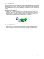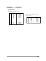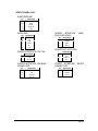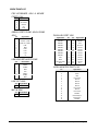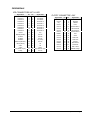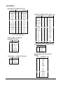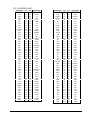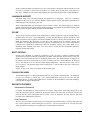
1
Advanced/RH LPX Motherboard Technical Product Specification Order Number 281809-003 April 1996 THIS SPECIFICATION [DOCUMENT] IS PROVIDED "AS IS" WITH NO WARRANTIES WHATSOEVER, INCLUDING ANY WARRANTY OF MERCHANTABILITY, FITNESS FOR ANY PARTICULAR PURPOSE, OR ANY WARRANTY OTHERWISE ARISING OUT OF ANY PROPOSAL, SPECIFICATION OR SAMPLE. No other license, express or implied, by estoppel or otherwise, to any other intellectual property rights is granted herein. Intel disclaims all liability, including liability for infringement of any proprietary rights, relating to implementation of information in this specification. Intel does not warrant or represent that such implementation(s) will not infringe such rights. A license is hereby granted to download a copy of this document for personal use only. This document is subject to change or update without notice. Readers should not design products based on this document. Technical updates should be obtained by calling Intel Literature or writing: Intel Corporation P.O. Box 7641 Mt. Prospect, Il 60056-7641 or call in North America 1-800-879-4683, Europe 44-0-1793-431-155, France 44-0-1793-421-777, Germany 44-0-1793-421-333, Japan (fax only) 81-0-120-478-832, other Countries 708-296-9333 Copyright 1996, Intel Corporation † Third-party brands and trademarks are the property of their respective owners. Advanced/RH Technical Product Specification • Page 2 Advanced/RH Technical Product Specification Table of Contents Introduction MOTHERBOARD MANUFACTURING OPTIONS BOARD LEVEL FEATURES LPX FORM FACTOR CPU PROCESSOR UPGRADE SECOND LEVEL CACHE SYSTEM MEMORY PERIPHERAL COMPONENT INTERCONNECT (PCI) PCISET NATIONAL SEMICONDUCTOR PC87306B SUPER I/O CONTROLLER GRAPHICS SUBSYSTEM AUDIO SUBSYSTEM UNIVERSAL SERIAL BUS (USB) 5 6 7 8 8 9 9 9 10 11 12 13 14 Connectors MOTHERBOARD CONNECTORS FRONT PANEL CONNECTIONS (J3A1, J2A1) AUDIO CONNECTORS BACK PANEL CONNECTORS 14 14 16 18 20 Power Consumption 21 Appendix A − User-Installable Upgrades SYSTEM MEMORY REAL TIME CLOCK BATTERY REPLACEMENT CPU UPGRADE GRAPHICS MEMORY UPGRADE HARDWARE MPEG MODULE 22 22 22 22 22 23 Appendix B − Configuration Jumper Settings CPU CONFIGURATION - JUMPER BLOCK J4L1(C&D) CMOS -J4L1 A PINS 4-6 PSWD -J4L1 A PINS 1-3 SETUP - J4L1 B PINS 1-3 RISER - J4G1 DRIVE OR OVERDRIVE - J6C2 RECOVERY JUMPER - J6C2 24 26 26 26 26 26 27 27 Appendix C − Memory Map 28 Appendix D − I/O Map 29 Appendix E − PCI Configuration Space Map 30 Appendix F − Interrupts & DMA Channels 31 Advanced/RH Technical Product Specification • Page 3 Appendix G − Connectors POWER SUPPLY FRONT PANEL−J3A1 BACK PANEL I/O PERIPHERALS MULTIMEDIA 32 32 33 34 35 36 Appendix-H Motherboard BIOS FLASH MEMORY IMPLEMENTATION BIOS UPGRADES SETUP UTILITY PCI AUTO-CONFIGURATION ISA PLUG ‘N’ PLAY ADVANCED POWER MANAGEMENT LANGUAGE SUPPORT PCI IDE BOOT OPTIONS FLASH LOGO AREA SECURITY FEATURES 39 39 39 40 40 40 40 41 41 41 41 41 Appendix I − PCI Configuration Error Messages 43 Appendix J− − AMIBIOS Error messages and Beep Codes BEEP CODES ERROR MESSAGES ERROR MESSAGES (CONT.) ISA NMI MESSAGES 44 44 44 45 45 Appendix K − Soft-off Control 46 Appendix L − Environmental Standards MOTHERBOARD SPECIFICATIONS 47 47 Appendix M − Reliability Data 48 Advanced/RH Technical Product Specification • Page 4 Introduction The Advanced/RH motherboard integrates the latest advances in processor, memory, and I/O technologies into a standard LPX form factor that provides leading edge technology. This combination of high integration and high performance makes the Advanced/RH motherboard the ideal platform for the increasing requirements of today's (and tomorrow's) desktop applications in the corporate workspace. The flexible LPX design will accept Pentium® processors operating at 75 MHz, 90 MHz, 100 MHz, 120 MHz, 133 MHz, 150 MHz and 166 MHz as well as future Pentium processors. The processor subsystem is complemented by a Revision 2.1 Card Edge Low Profile (CELP 2.1) socket that accepts either a 256 KB or 512 KB second level writeback cache module using pipelined synchronous burst technology. There is also an option for having 256 KB of Pipeline Burst SRAM soldered onto the motherboard. If cache memory is soldered on the motherboard, the CELP socket will not be installed. Only one type of cache may be used on the Advanced/RH motherboard. The memory subsystem is designed to support up to 512 MB of EDO DRAM (for improved performance) or standard Fast Page DRAM in standard 72-pin SIMM† sockets. A Type 7 Pentium OverDrive® socket provides an upgrade to future OverDrive processors. The Advanced/RH motherboard utilizes Intel's 82430HX PCIset to provide increased integration and performance over other motherboard designs. The Intel 82430HX PCIset contains an integrated PCI Bus Mastering IDE controller with two high performance IDE interfaces for up to four IDE devices (such as hard drives, CD-ROM readers, and so forth). The 82430HX PCIset coupled with the integration of the industry’s latest peripherals gives the user a robust computing platform. Complementing the 82439HX PCI controller is the 82371SB PIIX3 ISA bridge, offering new technology like USB expandability. The PIIX3 performs as a host on the Universal Serial Bus, and in the middle of 1996 Advanced/RH will provide connectors to accommodate USB peripherals. ATI† 264-VT video, with fast SGRAM video memory, provides excellent performance advantages over alternate solutions using EDO memory. ATI Media Connector modules, supplied by ATI Technologies, can be used to accelerate hardware MPEG and provide the tuner capabilities that previously required an entire add in card. Memory expansion modules, also supplied by ATI, can upgrade the motherboard from 1MB to 2 or 4 MB of SGRAM. The National PC87306B Super I/O controller integrates the standard PC I/O functions: floppy interface, two FIFO serial ports, one EPP/ECP capable parallel port, a Real Time Clock, keyboard controller, and support for an IrDA† compatible infrared interface. To provide for the increasing number of multimedia applications, a Creative† VIBRA16S audio CODEC is integrated onto the motherboard. Either consumer audio or business audio is selected by the OEM. Consumer audio will not have onboard jacks, like business audio, but will provide audio connections via an audio riser card. Either audio solution is provided by the VIBRA16S audio controller, and it provides 16-bit stereo, Sound Blaster Pro† compatible audio with full duplex capabilities to meet the demands of interactive multimedia applications. PCI and ISA expansion slots are supported by a connector on the motherboard designed to accept a riser card. In addition to superior hardware capabilities, a full set of software drivers and utilities are available to allow advanced operating systems such as Microsoft† Windows† 95 to take full advantage of the hardware capabilities. Features such as bus mastering IDE, Windows 95-ready Plug ‘N’ Play, Advanced Power Management (APM) with application restart, software-controlled power supply shutdown, and full duplex audio are all provided by software available for the Advanced/RH. Advanced/RH Technical Product Specification • Page 5 MOTHERBOARD MANUFACTURING OPTIONS The following manufacturing options are available. Details for each option are found in the corresponding section of this specification. AUDIO SUBSYSTEM Business audio Consumer audio No audio VIDEO SUBSYSTEM ATI VT graphic controller ATI CT graphic controller CACHE SUBSYSTEM Soldered SRAM CELP socket UNIVERSAL SERIAL BUS USB No USB Advanced/RH Technical Product Specification • Page 6 BOARD LEVEL FEATURES A B CD EFG H I J K L M N O P JJ II HH GG FF Q R EE DD S T CC U V BB AA W Z Y X OM04270 Figure 1. Advanced/RH Motherboard Features A − VGA† connector B − Parallel port connector C − COM2 Header D − COM2, or Dual in-line USB Connector E − COM1 connector F− Four Pin CD-ROM audio connector G − PS/2† Mouse port H − PS/2 Keyboard port I − Two 3.5 mm Audio Jacks (mic in, line out) J − Eight Pin Wave table upgrade connector K − 3 Pin Modem Audio Connector L − Creative Labs Vibra 16S audio, Yamaha† OPL3 FM synthesizer M − Midi Audio/Joystick connector N − Floppy connector O − Power Supply control connector P − 3.3v Power connector Q − Primary power connector R − Six SIMM sockets (three banks) S − PCI / ISA expansion connector T − National PC87306B I/O controller U − Flash BIOS V − PCI ISA/IDE Xcelerator (PIIX3) W − Battery for the Real-time clock X − Two PCI IDE interfaces Y − CPU 3.3v voltage regulator Z − Front Panel I/O connector AA − Socket 7 Pentium Processor socket BB − Celp 2.1 connector cache module socket CC − 82439HX controller (TXC) DD − 256K L2 PBSRAM EE − Riser Card 2/3 slot jumper FF − ATI Media Channel Connector for H/W MPEG GG − ATI graphics controller HH − Configuration jumper blocks II − Up to 2 MB graphics memory JJ − SGRAM Graphics memory upgrade header (This figure identifies the location of motherboard manufacturing options. Not all locations will be populated on all motherboards.) Advanced/RH Technical Product Specification • Page 7 LPX FORM FACTOR The Advanced/RH motherboard is designed to fit into a standard LPX form factor chassis. Figure 2 illustrates the mechanical form factor for the Advanced/RH. The Advanced/RH LPX form factor does adhere to the standard LPX guidelines in that the outer dimensions are 13” x 9”. Location of the I/O connectors, riser slot, and mounting holes are in strict compliance with the LPX specification. However, if business audio is selected by an OEM, a slight modification to the OEM’s chassis may be necessary to accept the audio jacks on the motherboard. 13.0 11.375 5.875 0.375 0.219 0.0 0.0 9.0 0.35 3.906 7.500 8.8125 OM04271 Figure 2. Advanced/RH Motherboard dimensions CPU The Advanced/RH LPX motherboard is designed to operate with 3.3 volt Pentium processors. The 3.3 volt power is provided by a patented on-board voltage regulator circuit. An on-board jumper enables use of VRE specified processors. The voltage regulator provides the required voltage for the processor from the 5 volt output of a standard power supply. Processors which run internally at 75, 90, 100, 120, 133, 150 and 166 MHz, and have iCOMP® ratings of 615, 735, 815, 1000, 1110, 1176 and 1308 respectively are supported. Future Pentium processors will also be supported. The Pentium processor maintains full backward compatibility with the 8086, 80286, Intel386 and Intel486 processors. It supports both read and write burst mode bus cycles, and includes separate 8 KB on-chip code and data write-back caches. Also integrated into the Pentium processor is an advanced numeric coprocessor which significantly increases the speed of floating point operations, while maintaining backward compatibility with the Intel486DX math coprocessor and complying to ANSI/IEEE standard 754-1985. Advanced/RH Technical Product Specification • Page 8 PROCESSOR UPGRADE The Advanced/RH motherboard is manufactured with the 321-pin (socket 7) ZIF processor socket. Socket 7 provides a processor upgrade path that includes higher performance Pentium OverDrive processors than can be supported with socket 5. The motherboard is built to support uniplane CPUs. However, a manufacturing option allows the socket 7 design to support split voltage planes that can supply different voltages for a processor’s CPU core and for the I/O core. Installing a split plane CPU into a motherboard configured only for uniplane processor may cause damage to the CPU. SECOND LEVEL CACHE The Intel 82430HX PCIset supports a second level cache that uses high performance Synchronous Pipeline Burst SRAM. Asynchronous cache is not supported by the 82430HX controller. Pipeline Burst (PB) SRAM provides performance similar to expensive Synchronous Burst SRAMs for only a slight cost premium over slower performing asynchronous SRAMs. As a manufacturing option, the Advanced/RH motherboard without onboard cache can be provided with a Card Edge Low Profile (CELP) version 2.1 socket that provides flexibility for second level cache options. The CELP socket can accommodate either a 256 KB or 512 KB cache module and is designed to work with modules that adhere to the COAST (Cache On A Stick) specification, version 2.1. The cache size is automatically detected and configured by the system BIOS for optimal performance. For a list of cache module suppliers or a copy of the COAST specification, contact your local Intel sales office or Intel authorized distributor. SYSTEM MEMORY The Advanced/RH motherboard provides six 72-pin SIMM sites for memory expansion. The sockets support 512 KB x 32 (2MB double sided SIMMs only), 1M x 32 (4 MB), 2M x 32 (8 MB), 4M x 32 (16 MB), 8M x 32 (32 MB), 16M x 32 (64MB), and 32M x 32 (128MB) single-sided or double-sided SIMM modules. Minimum memory size is 8 MB and maximum memory size, using four 32M x 32 SIMM modules, is 512 MB. Memory timing requires 70 ns fast page devices or, for optimum performance 60 ns EDO DRAM. 36-bit SIMM modules may be used for parity or ECC generation and checking. The six sockets are arranged as Bank 0, Bank 1, and Bank 2. Each bank consists of two sockets and provides a 64/72-bit wide data path. Both SIMMs in a bank must be of the same memory size and type, although each bank may have different types of memory installed. It is even possible to have 70 ns Fast Page DRAM in one bank and 60 ns EDO DRAM in the other, in which case each bank is independently optimized for maximum performance. Any combination of the banks may be populated. There are no jumper settings required for the memory size or type, which is automatically detected by the system BIOS. The Advanced/RH motherboard supports only tin-lead SIMMs. When banks 1 and 2 are populated at the same time, memory timing is modified from x333 to x444. This is due to loading on the address line shared by these two banks. In most applications the L2 cache will mask any performance degradation that is incurred. In addition, when using EDO Parity memory in an ECC configuration memory timing is changed from x222 to x333 to allow the chipset to perform Read Modify Writes. EDO DRAM Extended Data Out, or Hyper Page, DRAM is designed to improve the DRAM read performance. EDO DRAM holds the memory data valid until the next CAS# falling edge, unlike standard fast page mode DRAM which tri-states the memory data when CAS# negates to precharge for the next cycle. With EDO, the CAS# precharge overlaps the data valid time, allowing CAS# to negate earlier while still satisfying the memory data valid window time. Advanced/RH Technical Product Specification • Page 9 EXPANSION RISER An expansion slot riser connector of EISA form factor provides the capability to support either two or three PCI slots by changing a motherboard jumper to route any extra IRQ and ID selects. A riser board can also support up to five ISA expansion slots. The PCI bus is compliant with the PCI 2.1 specification. To ensure that the lowest positioned slot on the riser card can support a full length add-in card the following conditions must be met. 1) The minimum height requirement for the lowest positioned slot on the CPU side of the riser is 1.2”. Therefore the CPU heat sink should be no more than 1.2” high once installed on the processor. 2) The minimum height requirement for the lowest positioned slot on the SIMM side of the riser is 1.3”. Therefore, once SIMM memory is installed they should not be taller than 1.3”. PERIPHERAL COMPONENT INTERCONNECT (PCI) PCISET The Intel 82430HX PCIset is made up of two components: The 82439HX controller (TXC) and the 82371SB PCI ISA IDE Xcellerator (PIIX3) ISA bridge. The PCIset provides the following functions: • CPU interface control • Integrated L2 write-back cache controller – Pipeline Burst SRAM – 256 KB or 512 KB Direct Mapped • Integrated DRAM controller – 64/72-bit path to Memory – Support for EDO and Fast Page DRAM – 8 MB to 512 MB main memory – Parity and ECC support • Fully synchronous PCI bus interface – 25/30/33 MHz – PCI to DRAM > 100 Mbytes/sec • Interface between the PCI bus and ISA bus • Universal Serial Bus Controller (with B0 stepping of the PIIX 3) – Host/Hub Controller – Two USB ports • Integrated fast IDE interface – Support for up to 4 devices – PIO Mode 4 transfers up to 16 MB/sec – Integrated 8 x 32-bit buffer for Bus Master PCI IDE burst transfers – Bus Master mode • PCI 2.1 Compliant • Enhanced Fast DMA controller • Interrupt controller and steering • Counters/Timers • SMI interrupt logic and timer with Fast On/Off mode 82439HX TXC The 439HX controller provides all control signals necessary to drive a second level cache and the DRAM array, including multiplexed address signals. It also controls system access to memory and generates snoop controls to maintain cache coherency. The 439HX controller comes in a 324 pin Ball Grid Array package. 82371SB PCI ISA IDE XCELERATOR (PIIX3) The PIIX3 provides the interface between the PCI and ISA buses and integrates a dual channel fast IDE interface capable of supporting up to 4 devices. USB host/hub bus is provided by the PIIX 3. The PIIX3 integrates seven 32-bit DMA channels, five 16-bit timer/counters, two eight-channel interrupt controllers, PCI-to-AT interrupt mapping circuitry, NMI logic, ISA refresh address generation, and PCI/ISA bus arbitration circuitry onto the same device. The PIIX3 comes in a 208 pin QFP package. Advanced/RH Technical Product Specification • Page 10 IDE SUPPORT The Advanced/RH motherboard provides two independent high performance bus-mastering PCI IDE interfaces capable of supporting PIO Mode 3 and Mode 4 devices. The system BIOS supports Cylinder Sector Head (CHS), Logical Block Addressing (LBA) and Extended Cylinder Sector Head (ECHS) translation modes as well as ATAPI (e.g. CD-ROM) devices on both IDE interfaces. IDE device transfer rate and translation mode capability can be automatically determined by the system BIOS. Normally, programmed I/O operations require a substantial amount of CPU bandwidth. In multi-tasking operating systems like Microsoft Windows 95, the CPU bandwidth freed up by using bus mastering IDE can be used to complete other tasks while disk transfers are occurring. A driver is required for the IDE interface to operate as a PCI bus master capable of supporting PIO Mode 4 devices with transfer rates up to 22 MB/sec while minimizing the system demands upon the processor. Detailed information on the PCIset is available in the Intel 82430HX PCIset data sheet. NATIONAL SEMICONDUCTOR PC87306B SUPER I/O CONTROLLER Control for the integrated serial ports, parallel port, floppy drive, RTC and keyboard controller is incorporated into a single component, the National Semiconductor PC87306B. This component provides: • Two NS16C550-compatible UARTs with send/receive 16 byte FIFO — Support for an IrDA compliant Infra Red interface • Multi-mode bi-directional parallel port — Standard mode; IBM† and Centronics† compatible — Enhanced Parallel Port (EPP) with BIOS/Driver support — High Speed mode; Extended Capabilities Port (ECP) compatible • Industry standard floppy controller with 16 byte data FIFO (2.88 MB floppy support) • Integrated Real Time Clock accurate within +/- 13 minutes/yr at 25º C and 5 volts when the system is continuously powered on • Integrated 8042 compatible keyboard controller The PC87306B is normally configured by the BIOS automatically. However configuration of these interfaces is possible via the CMOS Setup program that can be invoked during boot-up. The serial ports can be enabled as COM1, COM2, IrDA, or disabled. The parallel port can be configured as normal, extended, EPP/ECP, or disabled. The floppy interface can be configured for 360 KB or 1.2 MB 5¼” media or for 720 KB, 1.2 MB, 1.44 MB, or 2.88 MB 3½” media. Header pins located near the back of the board allow cabling to use these interfaces FLOPPY CONTROLLER The PC87306B is software compatible with the DP8473 and 82077 floppy disk controllers. The floppy interface can be configured for 360 KB or 1.2 MB 5¼” media or for 720 KB, 1.2 MB, 1.44 MB, or 2.88 MB 3½” media in the BIOS setup. By default, the Floppy A interface is configured for 1.44 MB and Floppy B is disabled. Another setup option prevents the user from being able to write to floppy. Configuring the floppy interface for 1.2 MB 3 ½” (3-mode floppy) requires the use of a driver to operate correctly. KEYBOARD INTERFACE PS/2 keyboard/mouse connectors are located on the back panel side of the motherboard. The 5V lines to these connectors are protected with a PolySwitch† circuit which acts much like a self-healing fuse, re-establishing the connection after an over-current condition is removed. While this device eliminates the possibility of having to replace a fuse, care should be taken to turn off the system power before installing or removing a keyboard or mouse. The system BIOS can detect and correct keyboards and mice plugged into the wrong PS/2† style connector. Advanced/RH Technical Product Specification • Page 11 The integrated 8042 microcontroller contains the AMI Megakey keyboard/mouse controller code which, besides providing traditional keyboard and mouse control functions, supports Power-On/Reset (POR) password protection. The POR password can be defined by the user via the Setup program. The keyboard controller also provides for the following "hot key" sequences: • <CTRL><ALT><DEL>: System software reset. This sequence performs a software reset of the system by jumping to the beginning of the BIOS code and running the POST operation. • <CTRL><ALT><+> and <CTRL><ALT><->: Turbo mode selection. <CTRL><ALT><-> sets the system for deturbo mode, emulating an 25 MHz AT, and <CTRL><ALT><+> sets the system for turbo mode. Changing the Turbo mode may be prohibited by an operating system, or when the CPU is in Protected mode or virtual x86 mode under DOS. • <CTRL><ALT><defined in setup>: Power down and coffee-break key sequences take advantage of the SMM features of the Pentium Processor to greatly reduce the system’s power consumption while maintaining the responsiveness necessary to service external interrupts. REAL TIME CLOCK, CMOS RAM AND BATTERY The integrated Real Time Clock (RTC) is DS1287 and MC146818 compatible and provides a time of day clock and a 100-year calendar with alarm features. The RTC can be set via the BIOS SETUP program. The RTC also supports a 242-byte battery-backed CMOS RAM area in two banks. This area is reserved for BIOS use. The CMOS RAM can be set to specific values or cleared to the system default values using the BIOS SETUP program. Also, the CMOS RAM values can be cleared to the system defaults by using a configuration jumper on the motherboard. Table B-1, in Appendix B, lists the configuration jumper settings. An external coin-cell style battery provides power to the RTC and CMOS memory. The battery has an estimated lifetime of three years if the system is not plugged into the wall socket. When the system is plugged in, power is supplied from the LPX power supply’s 5v standby current to extend the life of the battery. See Appendix A for information regarding replacement batteries. IRDA (INFRA-RED) SUPPORT A 5-pin interface on the front panel I/O connector is provided to allow connection to a Hewlett Packard HSDSL1000 compatible Infra-red (IrDA) transmitter/receiver. Once the module is connected to the front panel I/O header, serial port 2 can be re-directed to the IrDA module, allowing the user to transfer files to or from portable devices such as laptops, PDA’s and printers using application software such as LapLink. The IrDA specification provides for data transfers at 115 Kbps from a distance of 1 meter. PARALLEL PORT The Parallel port can be configured in the BIOS setup as output only compatible mode, bi-directional mode, ECP or EPP modes. The highly flexible parallel port can also be assigned to I/O addresses 278H, 378H, or 3BCH and IRQ’s 5 or 7. Furthermore, a routable DMA scheme allows Plug ‘N’ Play operating systems such as Windows 95 to route either DMA channel 1 or 3 to the parallel port for ECP mode. EPP BIOS support must be provided by a device driver or TSR. GRAPHICS SUBSYSTEM The ATI-264VT controller is a highly integrated multimedia graphics & video controller for PCI bus systems. The VT achieves enhanced performance with an all in one design that integrates a video scaler, a color space converter, a true color palette DAC, and a triple clock synthesizer with ATI’s proven Mach64† graphics engine. The ATI-264VT controller is register compatible with ATI’s Mach64 accelerator series, and therefore is immediately compatible with a wide range of software applications and drivers. As a manufacturing option, the Advanced/RH board is also available with an ATI-264CT video controller and 1 MB of EDO video DRAM, upgradeable to a total of 2 MB by adding 1 MB of socketed video DRAM. Advanced/RH Technical Product Specification • Page 12 ATI-264VT RESOLUTIONS SUPPORTED BY THE MOTHERBOARD Resolution 640x480x4bpp 640x480x8bpp 640x480x16bpp 640x480x24bpp 640x480x32bpp 800x600x4bpp 800x600x8bpp 800x600x16bpp 800x600x24bpp 1024x768x4bpp 1024x768x8bpp 1024x768x16bpp 1280x1024x4bpp 1280x1024x8bpp 1 MB SGRAM X X X X X X X X X X 2 MB SGRAM X X X X X X X X X X X X X X Max Vertical Refresh Rate 100 Hz 100 Hz 100 Hz 100 Hz 60 Hz 100 Hz 100 Hz 100 Hz 100 Hz 100 Hz 100 Hz 100 Hz 75 Hz 75 Hz Table 1. Advanced/RH Audio resource mapping GRAPHICS DRIVERS AND UTILITIES Graphics drivers and utilities for Windows† 3.11 or for Windows 95 are supplied with the Advanced/RH motherboard. AUDIO SUBSYSTEM The Advanced/RH offers three audio options for the OEM. The consumer audio option uses an onboard header to route audio to a riser card in the I/O panel. Consumer audio also includes a wave table upgrade header for future expansion. The business audio option includes mike and line jacks on the motherboard next to the mouse and keyboard connectors. A third option is to have the board with no on-board audio. The Advanced/RH audio subsystem is based upon the Creative Labs Vibra 16S audio controller and Yamaha OPL3 FM synthesizer. The controller features a 16-bit stereo audio sub-system as a factory installed option along with the OPL3 FM synthesizer. The Vibra 16S controller provides all the digital audio and analog mixing functions required for recording and playing of audio on personal computers. These functions include stereo analog-to-digital and digital-to-analog converters, analog mixing, anti-aliasing and reconstruction filters, line and microphone level inputs, and digital audio compression via selectable A-law / µlaw, and full digital control of all mixer and volume control functions. VIBRA 16S RESOURCE MAP Base Address (software configured) 220H - 22FH(Default) or 240H - 24FH or 260H - 26FH or 280H - 28FH FM Address (fixed) 388H - 38BH Joystick Address/Game Port (fixed) 200H - 207H MPU-401 Address (software configured) 300H - 301H or 330H - 331H (default) MPU-401 Enable (software configured) Default is disabled Joystick Enable (software configured) Default Enabled Interrupt (Software configured) IRQ2/9 or IRQ5 (default) or IRQ7 or IRQ10 8-bit DMA Channel (software configured) DMA Channel 1 (default) or DMA Channel 3 16-bit DMA Channel (software configured) DMA channel 5 (default) DMA channel 7 Table 2. Advanced/RH Audio resource mapping Advanced/RH Technical Product Specification • Page 13 AUDIO DRIVERS Audio software and utilities are provided for the Advanced/RH motherboard. A Windows setup program installs all of the software programs and utilities onto the system hard drive. Included in the Creative audio software are DOS utilities that allow the user to play a CD-ROM, control sound volume and mixer settings, run diagnostics, and switch between Sound Blaster Pro and Windows Sound System modes. Windows drivers and utilities include the Windows sound driver, audio input control panel, audio mixer control panel, and a business audio transport utility. UNIVERSAL SERIAL BUS (USB) When B0 steppings of PIIX 3 are used in manufacturing, USB connectors may be added as a manufacturing option to support the new technology. The USB connector will occupy the serial 2 connector location, and there is a header to reroute COM2 to a breakout in the chassis or IO panel if the customer so desires. Connectors MOTHERBOARD CONNECTORS There are connectors on-board for Floppy, IDE, Graphics memory upgrade sockets, VESA† feature connector, SIMMs, CELP cache modules, battery holder and front panel I/O connectors. Advanced/RH Technical Product Specification • Page 14 PCI/ISA Expansion Connector(J6J2) CDROM J6N1 1 5 Simm Socket(6) Bank 0(J2D1, J2D2) Bank 1(J2E1, J2F1) Bank 2(J2E1, J2F1) 1 J9N2 4 Modem/Audio Connector 2 1 1 2 Floppy Drive 7 J9K2 J9K1 1 33 J9N1 8 Wave Table 3 PS Remote Connector 34 34 ATI Media Connector (J1H1) 33 1 3.3V Power MIDI Audio J9H1 CELP Connector (J1D1) 6 2 1 1 2 1 J9L1 Primary Power J9H1 PCI IDE Connector(2) J5C1 J6C1 39 40 12 J3A1 29 1 Front Panel I/O Connector OM04275 Figure 3. Advanced/RH connector locations Advanced/RH Technical Product Specification • Page 15 POWER SUPPLY CONTROL (J9H1,J9K2) When used with a power supply that supports remote power on/off, the Advanced/RH motherboard can turn off the system power via software control (“soft-off”). The Powerman utility supplied for Windows 3.1x allows for soft-off as does the shutdown icon in Windows 95 Start menu. The system BIOS will turn the system power off when it receives the proper APM command from the OS. For example, Windows 95 will issue this APM command when the user selects the “Shutdown the computer” option. Note that APM must be enabled in the system BIOS and OS in order for the soft-off feature to work correctly. Power supplies that support “soft-off” connect to the motherboard via the 3-pin “PWS CNTRL” connector, which is a Molex 2695 connector featuring a security latch for reliability. In order for the system to recognize the presence of a “soft-off” power supply, the supply must tie pin 3 of the PWS Control connector to ground. FRONT PANEL CONNECTIONS (J3A1, J2A1) The Advanced/RH motherboard provides header connectors to support functions typically located on the chassis bezel. Refer to Appendix G for exact pinout definitions for all of the connectors. Front panel features supported include: • System Speaker • Power LED • Infra-Red (IrDA) port • System Reset • Sleep/Resume • CPU fan • Hard Drive activity LED J3A1 29 1 SPKR IR SLP/PS-ON HDLED PWRLED RST FAN OM04279 Figure 4. Front Panel I/O Connectors Advanced/RH Technical Product Specification • Page 16 SPEAKER The external speaker provides error beep code information during the Power-On Self Test if the system cannot use the video interface. If no speakers are plugged into the audio output jack, the audio output is redirected to the external PC speaker. SLEEP / RESUME When Advanced Power Management (APM) is activated in the system BIOS and the operating system’s APM driver is loaded, Sleep mode (Stand-By) can be entered in one of three ways: an optional front panel “Sleep/Resume” button, a user defined keyboard hot key, or prolonged system inactivity. The Sleep/Resume button is supported by a 2-pin header located on the front panel I/O connector. Closing the “Sleep” switch will generate an SMI (System Management Interrupt) to the processor which immediately goes into System Management Mode (SMM), the so called “Sleep” mode. The front panel “Sleep mode” switch must be a momentary two pin SPST type that is normally open. The function of the Sleep/Resume button can also be achieved via a keyboard hot-key sequence, or by a time-out of the system inactivity timer. Both the keyboard hot-key and the inactivity timer are programmable in the BIOS setup (timer is set to 10 minutes by default). To re-activate the system, or “Resume”, the user must simply press the sleep/resume button again, or use the keyboard or mouse. Note that mouse activity will only “wake up” the system if a mouse driver is loaded. While the system is in Stand-By or “sleep” mode it is fully capable of responding to and servicing external interrupts (such as incoming fax) even though the monitor will only turn on if a user interrupt (keyboard/mouse) occurs as mentioned above. This interface is also supported by pins 1 and 2 of the PS SLEEP connector. INFRA-RED (IRDA) CONNECTOR Serial port 2 can be configured to support an IrDA module via a 5 pin header connector . Once configured for IrDA, the user can transfer files to or from portable devices such as laptop computers, PDA’s or printers using application software such as Traveling Software’s LapLink. The IrDA specification provides for data transfers at 115 Kbps from a distance of 1 meter. RESET This 2-pin header can be connected to a momentary SPST type switch that is normally open. When the switch is closed, the system will hard reset and run POST. Advanced/RH Technical Product Specification • Page 17 AUDIO CONNECTORS There are two methods of accessing the audio features on the Advanced/RH. The method installed depends on the audio option that has been selected. For business audio, audio is accessed using audio jacks provided on the motherboard. These two 1/8” jacks supply Line Out, and Mic In connections and are available through the back I/O panel. MIDI/AUDIO I/O CONNECTOR Consumer audio is provided by using an audio riser card connected to the audio/midi connector of the motherboard. The audio riser card contains all of the necessary audio jacks (Speaker Out, Line In, Mic In) and the game port. It plugs into a 34-pin header connector on the motherboard. An example of the consumer audio riser card is shown below. The audio connectors are 1/8” stereo jacks . Figure 5. Advanced/RH Consumer audio I/O module CD-ROM AUDIO INPUT A four pin connector is provided for interfacing the audio output stream from a CD-ROM reader into the audio sub-system mixer. This connector is compatible with the typical cable that is supplied with CDROM readers for interfacing to audio add-in cards. This feature is available in both consumer and business audio options. Advanced/RH Technical Product Specification • Page 18 WAVE TABLE UPGRADE An eight pin header is provided as part of the consumer audio option to connect to a wave table upgrade card for richer sound quality in both DOS and Windows environments. The wave table upgrade module is simply installed into a standard ISA slot with a cable routed to the connector. Compatible wave table upgrade cards are available from several venders; the ICS WaveFront upgrade module and the CrystaLake Series 2000 wave table product family add a complete General MIDI compatible music solution to the Advanced/RH based system. For more information on CrystaLake products Contact CrystaLake Mulitmedia at http://www.teleport.com/~crystal, or (503) 222-2603 ext. 209 Figure 6. Advanced/RH Wave Table Upgrade module Advanced/RH Technical Product Specification • Page 19 BACK PANEL CONNECTORS The back panel provides external access to PS/2 style keyboard and mouse connectors as well as two serial and one parallel port, which are integrated on the Advanced/RH motherboard. If a USB connector is present, COM2 can be routed to a back panel knockout from the COM2 header on the motherboard. Audio jacks for Speaker Out and Microphone are provided for business audio on the back I/O panel. By adding an audio riser for consumer audio solutions a Midi/Game port can be made available through an ISA panel. Figure 5 shows the general location of the I/O connectors. Business audio jacks and the consumer audio/midi riser are mutually exclusive features. PS/2 Keyboard Audio Jacks COM 1 COM 2 Parallel Port VGA PS/2 Mouse OM04272 Figure 7. Back Panel I/O Connectors Advanced/RH Technical Product Specification • Page 20 Power Consumption Tables 3 and 4 list the measured current and voltage requirements for the Advanced/RH motherboard configured with 16 MB of DRAM. Table 5 lists the typical power consumed by the same configuration.. This information is preliminary and is provided only as a guide for calculating approximate total system power usage with additional resources added. Voltage DC Voltage +3.3V +5V +5V SB (stand by) -5V +12V -12V Acceptable tolerance +/- 5% +/- 5% +/- 5% +/- 5% +/- 5% +/- 5% Table 3. Advanced/RH Voltage tolerance Current and Power AC (watts) +5v No APM enabled DOS prompt Windows95 @1024x768 APM enabled DOS prompt Windows95 @1024x768 Suspended DC (amps) +12v 28 28 3.5A 4.0A 160mA 160mA 24.3 24.4 20.3 2.2A 2.2A 2.2A 160mA 160mA 160mA Table 4. Advanced/RH Power and Current Requirements System Configuration System Configuration Advanced/RH motherboard, 166 MHz Pentium Processor, 24 MB EDO RAM, 256 KB PBSRAM L2 cache, Floppy drive, 1.6 GB hard drive, Sony CDU-77E CD-ROM drive Table 5. Power use by System Resources Advanced/RH Technical Product Specification • Page 21 Appendix A − User-Installable Upgrades SYSTEM MEMORY Supported SIMM Sizes Bank Size Note 512K x 32 (2 MB) 4MB 1 1M x 32 (4 MB) 8MB 2M x 32 (8 MB) 16MB 4M x 32 (16 MB) 32MB 8M x 32 (32 MB) 64MB 2 16M x 32 (64MB) 128MB 2 32M x 32 (128MB) 256MB 2 Table A-1. Supported Memory SIMM Sizes and Configuration Note 1: 512K x 32 SIMMs are supported, however, they must be double sided SIMMs Note: 2 When using Single Sided High Density SIMMs such as 32 MB single sided, 64 MB double sided, or 128 MB SIMMs, SIMMs that have less than 32 MB per side will NOT be recognized in the system. The Advanced/RH will support both Fast Page DRAM or EDO DRAM SIMMs, but they cannot be mixed within the same memory bank. If Fast Page DRAM and EDO DRAM SIMMs are installed in separate banks, each bank will be optimized for maximum performance. Parity or ECC generation and detection are supported when parity SIMMs are the only SIMMs present on the motherboard. SIMM requirements are 70 ns Fast Page Mode or 60 ns EDO DRAM with tin-lead connectors. 8 MB is the minimum memory size supported by the Advanced/RH motherboard. 512 MB is the maximum memory that can be supported in any combination of SIMMs from the table. REAL TIME CLOCK BATTERY REPLACEMENT The battery can be replaced with a Sanyo CR2032, or equivalent, coin cell lithium battery. This battery has a 220 mAh rating. CPU UPGRADE A Type 7 Zero Insertion Force (ZIF) socket provides users with a performance upgrade path to the P54CTB OverDrive technology. LPX form factor makes it easier for the end user to replace the processor. GRAPHICS MEMORY UPGRADE The ATI-264VT graphics subsystem has either 1 or 2MB of SGRAM soldered down on the base board. Video memory can be upgraded with a daughter card that is compatible with ATI PCI add in cards. Information on the memory upgrade can be obtained by contacting ATI Technologies at the numbers listed below in the HARDWARE MPEG MODULE section. Advanced/RH Technical Product Specification • Page 22 HARDWARE MPEG MODULE ATI provides a hardware MPEG module that will work with the Advanced/RH. This module mounts onto connector J1H1, and uses mounting holes provided on the motherboard. This modul is also known as the ATI Multimedia Controller, or AMC. For more information contact ATI Technologies at http://www.atitech.ca, or (905) 882-2626 . . . . . Customer Support (voice) (905) 882-0546 . . . . . Customer Support (fax) (905) 764-9404 . . . . . ATI DOWNLOAD BBS (8N1) Advanced/RH Technical Product Specification • Page 23 Appendix B − Configuration Jumper Settings 3 2 1 6 5 4 D 6 5 4 C 6 5 4 B 6 5 4 A 6 5 4 13.00" 3 2 1 3 2 1 3 2 1 3 2 1 J4L1 J4G1 Clock Speed, CMOS, Password Riser Jumpers 4 5 6 1 2 3 J6C2 OverDrive Voltage Jumper Figure B-1. Configuration Jumper locations Advanced/RH Technical Product Specification • Page 24 FUNCTION FREQ ** (Note: These jumpers also set PCI, and ISA clock speeds.) MULT (cpu clock multiplier) CMOS (resets CMOS settings to default) PSWD (Password Clear) SETUP (CMOS Setup Access) RISER (Select # of PCI slots on riser) Recovery Drive or OverDrive Processor Voltage ** * Default configuration ** As shipped JUMPER BLOCK CONFIGURATION See table B-2 below J4L1(C) J4L1(D) See table B-2 below J4L1(A) * 4-5 Keep (normal) 5-6 CLR (reset to default) * 1-2 Keep (Password Enabled) 2-3 CLR (Password Clear/Disabled) * 1-2 ENBL (Access Allowed) 2-3 DIS (Access Denied) * 1-2 & 4-5 2 SLOTS 2-3 & 5-6 3 SLOTS *1-2 Normal operation 2-3 Recovery mode *5-6- Default voltage (VRE) 4-5 OverDrive processor voltage (VR) J4L1(A) J4L1(B) J4G1 J6C2 J6C2 Table B-1. Configuration Jumper settings Advanced/RH Technical Product Specification • Page 25 CPU CONFIGURATION - JUMPER BLOCK J4L1(C&D) These allow the motherboard to be switched between different speeds of the Pentium processor. These jumpers also affect the PCI and ISA clock speeds according to the following table: CPU Freq. (MHz) 166 150 133 120 100 90 75 reserved Host Bus Freq. (MHz) 66 60 66 60 66 60 50 - Host Bus pins J4L1C 1-3 1-2 2-3 1-2 2-3 1-2 2-3 2-3 1-2 Host Bus pins J4L1C 4-6 5-6 4-5 5-6 4-5 5-6 4-5 5-6 4-5 CLK Ratio 5/2 5/2 2 2 3/2 3/2 3/2 - Clk Ratio pins J4L1D 1-3 2-3 2-3 2-3 2-3 1-2 1-2 1-2 X Clk Ratio pins J4L1D 4-6 5-6 5-6 4-5 4-5 4-5 4-5 4-5 X PCI Freq. (MHz) 33 30 33 30 33 30 25 - Table B-2. CPU/SYSTEM speed settings (* default setting) The ISA clock is derived from the PCI bus clock. The BIOS automatically sets the ISA clock speed to one fourth of the PCI frequency. PCI Frequency ISA clock speed 25 MHz 6.25 MHz 30 MHz 7.5 MHz 33 MHz 8.25 MHz Table B-3. ISA clock settings set by the BIOS based on PCI Clk Speed CMOS -J4L1 A PINS 4-6 Allows CMOS settings to be reset to default values by moving the jumper from pins 4-5 to pins 5-6 and turning the system on. When the system reports “NVRAM cleared by jumper”, the system can be turned off and the jumper should be returned to the 4-5 position to restore normal operation. This procedure should be done whenever the system BIOS is updated. Default is for this jumper to be on pins 4-5. PSWD -J4L1 A PINS 1-3 Allows system password to be cleared by moving the jumper from pins 1-2 to pins 2-3 and turning the system on. The system should then be turned off and the jumper should be returned to the 1-2 position to restore normal operation. This procedure should only be done if the user password has been forgotten. The password function is effectively disabled if this jumper is in the 2-3 position. Default is for the password to be enabled (1-2 position). SETUP - J4L1 B PINS 1-3 Allows access to CMOS Setup utility to be disabled by moving this jumper from the 1-2 position to the 2-3 position. Default is for access to setup to be enabled (1-2 position). RISER - J4G1 The riser jumper block allows routing of an extra IRQ and ID select to the riser card for an additional PCI slot to support a maximum of 3 PCI slots on a riser. Default is set for 2 PCI slots on the riser card (1-2 position and 4-5 position). Advanced/RH Technical Product Specification • Page 26 DRIVE OR OVERDRIVE - J6C2 Sets the CPU voltage to either standard voltage (3.3v), or OverDrive (3.6v). The Default setting is for a jumper to connect pin 5-6 for standard voltage. Move the jumper to connect pins 4-5 to select OverDrive voltage. RECOVERY JUMPER - J6C2 This jumper should be set to normal mode, Pins 1-2, and should only be moved when a recovery is being performed, i.e. jumper 2-3. Advanced/RH Technical Product Specification • Page 27 Appendix C − Memory Map Address Range 1024K-512M 960K-1023K Address Range 100000-20000000 F0000-FFFFF Size 511M 64K Description Extended Memory AMI System run time BIOS 944K-959K EC000-EFFFF 16K Main BIOS Recovery Code 936K-943K EA000-EBFFF 8K ESCD (Plug ‘N’ Play configuration area) 928K-935K E8000-E9FFF 8K OEM LOGO (available as UMB) 896K-927K E0000-E7FFF 32K BIOS RESERVED (Currently available as UMB) 800-895K C8000-DFFFF 96K Available HI DOS memory (open to ISA and PCI bus) 640K-799K A0000-C7FFF 160K 639K 9FC00-9FFFF 1K 512K-638K 80000-9FBFF 127K Extended conventional 0K-511K 00000-7FFFF 512K Conventional Off-board video memory and BIOS Extended BIOS Data (moveable by QEMM, 386MAX) Table C-1. Advanced/RH Memory Map The table above details the Advanced/RH memory map. The ESCD area from EA000-EBFFF is not available for use as an Upper Memory Block (UMB) by memory managers. The area from E0000-E7FFF is currently not used by the BIOS and is available for use as UMB by memory managers. Parts of this area may be used by future versions of the BIOS to add increased functionality. Advanced/RH Technical Product Specification • Page 28 Appendix D − I/O Map Address (hex) 0000 - 000F 0020 - 0021 Size 16 bytes 2 bytes Description PIIX - DMA 1 PIIX - Interrupt Address (hex) 0388 - 038B 03B4 - 03B5 Size 4 bytes 2 bytes 002E - 002F 2 bytes Ultra I/O configuration 03BA 1 byte 0040 - 0043 4 bytes PIIX - Timer 1 03BC - 03BF 4 bytes 0048 - 004B 4 bytes PIIX - Timer 2 03C0 - 03CA 12 bytes Description Parallel Port 3 0060 1 byte Keyboard Controller 03CC 1 byte 0061 1 byte PIIX - NMI, speaker 03CE - 03CF 2 bytes 0064 1 byte Kbd Controller, 03D4 - 03D5 2 bytes 0070, bit 7 1 bit PIIX - Enable NMI 03DA 1 byte 0070, bits 6:0 7 bits PIIX - Real Time 03E8 - 03EF 8 bytes Serial Port 3 0071 1 byte PIIX - Real Time 03F0 - 03F5 6 bytes Floppy Channel 0078 1 byte Reserved - Brd. 03F6 1 byte Pri IDE Chan 0079 1 byte Reserved - Brd. 03F7 (Write) 1 byte Floppy Chan 1 0080 - 008F 16 bytes PIIX - DMA Page 03F7, bit 7 1 bit Floppy Disk 00A0 - 00A1 2 bytes PIIX - Interrupt 03F7, bits 6:0 7 bits Pri IDE Chan 00C0 - 00DE 31 bytes PIIX - DMA 2 03F8 - 03FF 8 bytes On-Board Serial 00F0 1 byte Reset Numeric Error LPT + 400h 8 bytes ECP port, LPT 0170 - 0177 8 bytes Secondary IDE 04D0 - 04D1 2 bytes Edge/Level 01F0 - 01F7 8 bytes Primary IDE Channel 0608 - 060B 4 bytes 0200 - 0207 8 bytes Game Port 0CF8* 4 bytes PCI Config 0220 - 022F 8 bytes 0CF9 1 byte Turbo & Reset 0278 - 027B 4 bytes Parallel Port 2 0CFC-0CFF 4 bytes PCI Config Data 02F8 - 02FF 8 bytes On-Board Serial Port 2 0FF0 - 0FF7 8 bytes 0330 - 0331 1 bytes MPU - 401 (MIDI) FF00 - FF07 8 bytes IDE Bus Master 0376 1 byte Sec IDE Chan Cmd FFA0 - FFA7 8 bytes IDE primary FFA8 - FFAF 8 bytes IDE secondary 0377 1 byte Sec IDE Chan Stat 0378 - 037F 8 bytes Parallel Port 1 Table D-1. Advanced/RH I/O Address Map I/O Port 78 is reserved for BIOS use. Port 79 is a read only port, the bit definitions are shown below in Table D-2. Bit # 0 1 2 3 4 5 6 7 Description Reserved Soft Off capable power supply present Onboard Audio present External CPU clock External CPU clock Setup Disable Clear CMOS Password Clear Bit = 1 n/a No Yes Table B-2 Table B-2 Enable access Keep values Keep password Bit = 0 n/a Yes No Table B-2 Table B-2 Disable access Clear values Clear password Table D-2. Advanced/RH Port 79 Definition Advanced/RH Technical Product Specification • Page 29 Appendix E − PCI Configuration Space Map The 82430HX PCIset uses Configuration Mechanism 1 to access PCI configuration space. The PCI Configuration Address register is a 32-bit register located at CF8h, the PCI Configuration Data register is a 32-bit register located at CFCh. These registers are only accessible by full DWORD accesses. The table below lists the PCI bus and device numbers used by the motherboard. Bus Number (h ) 00 00 Dev Number (hex) 00 07 Func. Number (h ) 00 00 Description 00 07 01 Intel 82371FB (PIIX 3) IDE Bus Master 00 08 00 Video [ATI] 00 0B 00 Option PCI expansion Slot for 3 Slot Riser 00 11 00 PCI Expansion Slot 00 13 00 PCI Expansion Slot Intel 82437HX Intel 82371FB (PIIX 3) PCI/ISA bridge Table E-1. Advanced/RH PCI Configuration. Space Map Advanced/RH Technical Product Specification • Page 30 Appendix F − Interrupts & DMA Channels IRQ System Resource NMI 0 I/O Channel Check Reserved, Interval Timer 1 Reserved, Keyboard buffer full 2 Reserved, Cascade interrupt from slave PIC 3 Serial Port 2 4 Serial Port 1 5 Audio 6 Floppy 7 Parallel Port 1 8 Real Time Clock 9 User available 10 User available 11 Audio 12 Onboard Mouse Port 13 Reserved, Math coprocessor 14 15 Primary IDE Secondary IDE if present, else user available Table F-1. Advanced/RH Interrupts DMA Data Width System Resource 0 1 8- or 16-bits 8- or 16-bits Audio Audio 2 8- or 16-bits Floppy 3 8- or 16-bits Parallel Port (for ECP/EPP Config.) 4 Reserved - Cascade channel 5 16-bits Open 6 16-bits Open 7 16-bits Open Table F-2. Advanced/RH DMA Map Advanced/RH Technical Product Specification • Page 31 Appendix G − Connectors POWER SUPPLY PRIMARY POWER J9H1 Pin Name Function 1 2 PWRGD +5 V Power Good + 5 volts Vcc 3 +12 V + 12 volts 4 -12 V - 12 volts 5 GND Ground 6 GND Ground 7 GND Ground 8 GND Ground 9 -5 V -5 volts 10 +5 V + 5 volts Vcc 11 +5 V + 5 volts Vcc 12 +5 V + 5 volts Vcc PCI (3.3V) POWER J9J1 NOT POPULATED Pin Name Function 1 2 GND GND Ground Ground 3 GND Ground 4 +3.3 V + 3.3 volts 5 +3.3V + 3.3 volts 6 +3.3 V + 3.3 volts Advanced/RH Technical Product Specification • Page 32 FRONT PANEL− J3A1 SLEEP/RESUME Pin Signal Name 15 16 SW_ON GND 17 SLEEP 18 SLEEPPU 19 KEY INFRA-RED Pin Signal Name 25 24 CONIRRX IRTX 23 POWER INTERFACE DRIVE LED (DISK) Pin Signal Name GND 14 13 PWRPU PWDRV 22 IRRIN 12 HDA 21 NC 11 HDPU 20 VCC HARD POWER LED / KEYLOCK POWER INTERFACE CPU FAN Signal Name 3 2 Ground +12V 31 Ground POWER INTERFACE SPEAKER CONNECTOR Signal Name 10 9 PWDRV NC 8 PWRPU 7 KEY POWER INTERFACE CONNECTOR Pin Signal Name Pin Signal Name 29 28 GND Key 6 5 Key RESET 27 SPKSRC 4 Ground 26 SPKOUT RESET Advanced/RH Technical Product Specification • Page 33 BACK PANEL I/O PS/2 KEYBOARD J8N1 & MOUSE PORTS J7N1 Pin Signal Name 1 2 Data No Connect 3 Ground 4 Vcc 5 Clock SERIAL PORTS COM1 J6N2 & COM2 J5N1 PARALLEL PORT J3N1 Pin Signal Name 1 2 DCD Serial In - (SIN) Signal Name STROBEData Bit 0 Pin 1 2 Pin 14 15 3 Serial Out - (SOUT) Data Bit 1 3 16 INIT- 4 DTR- Data Bit 2 4 17 SLCT IN- 5 GND Data Bit 3 5 18 Ground 6 DSR- Data Bit 4 6 19 Ground 7 RTS- Data Bit 5 7 20 Ground 8 CTS- Data Bit 6 8 21 Ground 9 RI Data Bit 7 9 22 Ground ACK- 10 23 Ground USB J5N2 REPLACES COM2 Signal Name AUTO FEEDERROR- BUSY 11 24 Ground Pin Signal Name PE (Paper End) 12 25 Ground 1 2 VCC USBP0- SLCT 13 26 N.C. 3 USBP0 4 GND Pin Signal Name 5 VCC 6 USBP1- 1 2 Red Green 7 USBP1 3 Blue 8 GND 4 No Connect 5 Ground 6 Ground Signal Name 7 Ground Line Out 8 Ground 9 No Connect LINE OUT J9N2 Pin 1 MIC IN J8N2 Pin Signal Name 1 Line Out VIDEO MONITOR PORT J1N1 10 Ground 11 No Connect 12 MONID1 13 Horizontal Sync. 14 Vertical Sync. 15 MONID2 Advanced/RH Technical Product Specification • Page 34 PERIPHERALS IDE CONNECTORS J5C1 & J6C1 Signal Name Reset IDE Host Data 7 Pin 1 3 Pin 2 4 Host Data 6 5 6 Host Data 9 Host Data 5 7 8 Host Data 10 Host Data 4 9 10 Host Data 11 Host Data 3 11 12 Signal Name Ground Host Data 8 Host Data 12 Host Data 2 13 14 Host Data 13 Host Data 1 15 16 Host Data 14 Host Data 0 17 18 Host Data 15 Ground 19 20 Key DDRQ0 (DDRQ1) 21 22 Ground I/O Write- 23 24 Ground I/O Read- 25 26 Ground IOCHRDY 27 28 Vcc pull-up DDACK0 (DDACK1)- 29 30 Ground IRQ14 (IRQ15) 31 32 NC Addr 1 33 34 NC Addr 0 35 36 Addr 2 Chip Select 1P (1S)- 37 38 Chip Select 3P (3S)- Activity- 39 40 Ground FLOPPY CONNECTOR J9K1 Signal Name Ground Ground Pin 1 3 Pin 2 4 Signal Name DENSEL Reserved FDEDIN Key 5 6 Ground 7 8 Index- Ground 9 10 Motor Enable A- Ground 11 12 Drive Select B- Ground 13 14 Drive Select A- Ground 15 16 Motor Enable B- MSEN1 17 18 DIR- Ground 19 20 STEP- Ground 21 22 Write Data- Ground 23 24 Write Gate- Ground 25 26 Track 00- MSEN0 27 28 Write Protect- Ground 29 30 Read Data- Ground 31 32 Side 1 Select- Ground 33 34 Diskette Change- Advanced/RH Technical Product Specification • Page 35 MULTIMEDIA MIDI/AUDIO CONNECTOR J9L1 Signal Name +5 V JoyStick But0 Pin 1 3 Pin 2 4 Signal Name +5 V JoyStick But2 JoyStick X1 5 6 JoyStick X2 Ground 7 8 MIDI Out Ground 9 10 JoyStick Y2 JoyStick Y1 11 12 JoyStick But3 JoyStick But1 13 14 MIDI In +5 V 15 16 Key Key 17 18 Key Line Out Right 19 20 Ground Right Speaker 21 22 Ground Left Speaker 23 24 Key Line Out Left 25 26 Ground Line In Right 27 28 -12 V ATI MULTI-MEDIA CON. (AMC) J1H1 Signal Name Ground Ground Pin 1 3 Pin 2 4 Signal Name Data 0 Data 1 Ground 5 6 Data 2 Data enable 7 8 Data 3 Sync enable 9 10 Data 4 PCLK enable 11 12 Data 5 SDA 13 14 Data 6 Ground 15 16 Data 7 Ground 17 18 DCLK Ground 19 20 BLANK VFCSNS 21 22 HSYNC SCL 23 24 VSYNC KEY 25 26 GND key 27 28 key VCC 29 30 SA RST 31 32 SNRDY SAD 33 34 VMASK NC 35 36 Signal Name GND 37 38 +12V 1 2 Wave Right Ground NC 39 40 NC 3 Wave Left 4 Ground Pin Signal Name 5 Key 6 Ground 1 2 Ground CD-LEFT 7 MIDI_Write 3 Ground 8 MIDI_OUT 4 CD-Right Line In Left 29 30 Ground Mic In 31 32 +12 V Ground 33 34 Ground (NOT A MM OPTION) WAVE TABLE UPGRADE CONNECTOR J9N1 Pin TELEPHONY CONNECTOR J9L2 CD-ROM AUDIO INTERFACE J6N1 MIDI/GAME PORT (ON AUDIO RISER) Pin Signal Name 1 2 Vcc JSBUT0 3 JSX1R 4 GND Pin Signal Name 1 2 Ground Mono Out 3 Mic In 4 No Connect 5 GND 6 JSY1R 7 JSBUT1 8 Vcc 9 Vcc 10 JSBUT2 11 JSX2R 12 MIDI-OUT-R 13 JSY2R 14 JSBUT3 15 MIDI-IN-R Advanced/RH Technical Product Specification • Page 36 PCI / ISA RISER (J6J2) Signal Name Pin Pin Signal Name Signal Name Pin Pin Signal Name IOCHKSD7 A1 A2 B1 B2 GND RSTDRV GND GND E1 E2 F1 F2 GND GND SD6 A3 B3 Vcc PCIINT0- E3 F3 PCIINT2- SD5 A4 B4 IRQ9 PCIINT1- E4 F4 PCIINT3- SD4 A5 B5 -5V Vcc E5 F5 Vcc SD3 A6 B6 DRQ2 Key E6 F6 Key SD2 A7 B7 -12V Vcc E7 F7 Vcc PCLKF SD1 A8 B8 0WS- PCIRST- E8 F8 SD0 A9 B9 +12V GNT0- E9 F9 GND IOCHRDY A10 B10 GND REQ0- E10 F10 GNT1- AEN A11 B11 SMEMW- GND E11 F11 GND SA19 A12 B12 SMEMR- PCLKE E12 F12 REQ1- SA18 A13 B13 IOW- GND E13 F13 AD31 SA17 A14 B14 IOR- AD30 E14 F14 AD29 SA16 A15 B15 DACK3- 3.3V E15 F15 3.3V SA15 A16 B16 DRQ3 Key E16 F16 Key SA14 A17 B17 DACK1- 3.3V E17 F17 3.3V SA13 A18 B18 DRQ1 AD28 E18 F18 AD27 SA12 A19 B19 REFRESH- AD26 E19 F19 AD25 SA11 A20 B20 SYSCLK AD24 E20 F20 CBE3- SA10 A21 B21 IRQ7 AD22 E21 F21 AD23 SA9 A22 B22 IRQ6 AD20 E22 F22 AD21 SA8 A23 B23 IRQ5 AD18 E23 F23 AD19 SA7 A24 B24 IRQ4 3.3V E24 F24 3.3V SA6 A25 B25 IRQ3 Key E25 F25 Key SA5 A26 B26 DACK2- 3.3V E26 F26 3.3V SA4 A27 B27 TC AD16 E27 F27 AD17 SA3 A28 B28 BALE FRAME- E28 F28 IRDY- SA2 A29 B29 Vcc CBE2- E29 F29 DEVSEL- SA1 A30 B30 OSC TRDY- E30 F30 PLOCK- SA0 A31 B31 GND STOP- E31 F31 PERR- SBHE- C1 D1 MEMCS16- SDONE G1 H1 SERR- LA23 C2 D2 IOCS16- SBO- G2 H2 AD15 LA22 C3 D3 IRQ10 CBE1- G3 H3 AD14 LA21 C4 D4 IRQ11 PAR G4 H4 AD12 LA20 C5 D5 IRQ12 GND G5 H5 GND LA19 C6 D6 IRQ15 Key G6 H6 Key LA18 C7 D7 IRQ14 GND G7 H7 GND LA17 C8 D8 DACK0- AD13 G8 H8 AD10 MEMR- C9 D9 DRQ0 AD11 G9 H9 AD8 MEMW- C10 D10 DACK5- AD9 G10 H10 AD7 SD8 C11 D11 DRQ5 CBE0- G11 H11 AD5 SD9 C12 D12 DACK6- AD6 G12 H12 AD3 SD10 C13 D13 DRQ6 AD4 G13 H13 AD1 SD11 C14 D14 DACK7- AD2 G14 H14 AD0 SD12 C15 D15 DRQ7 Key G15 H15 Key SD13 C16 D16 Vcc Vcc G16 H16 Vcc SD14 C17 D17 MASTER- Vcc G17 H17 Vcc SD15 C18 D18 GND GND G18 H18 GND GND G19 H19 GND Advanced/RH Technical Product Specification • Page 37 CELP 2.1 CONNECTOR (J1D1) Signal Name Pin Pin Signal Name Signal Name Pin Pin Signal Name GND TIO0 1 2 41 42 D58 D56 GND TIO1 81 82 121 122 D59 D57 TIO2 3 43 GND TIO7 83 123 GND TIO6 4 44 D54 TIO5 84 124 D55 TIO4 5 45 D52 TIO3 85 125 D53 TIO8 6 46 D50 TI09 86 126 D51 VCC3 7 47 D48 VCC5 87 127 D49 TWE* 8 48 GND TIO10 88 128 GND CADS* 9 49 D46 CADV* 89 129 D47 GND 10 50 D44 GND 90 130 D45 CWE4* 11 51 D42 COE* 91 131 D43 CWE6* 12 52 VCC3 CWE5* 92 132 VCC5 CWE0* 13 53 D40 CWE7* 93 133 D41 CWE2* 14 54 D38 CWE1* 94 134 D39 VCC3 15 55 D36 VCC5 95 135 D37 CCS* 16 56 GND CWE3* 96 136 GND GWE* 17 57 D34 CAB3 97 137 D35 BWE* 18 58 D32 CALE 98 138 D33 GND 19 59 D30 GND 99 139 D31 A3 20 60 VCC3 RSVD 100 140 VCC5 A7 21 61 D28 A4 101 141 D29 A5 22 62 D26 A6 102 142 D27 A11 23 63 D24 A8 103 143 D25 A16 24 64 GND A10 104 144 GND VCC3 25 65 D22 VCC5 105 145 D23 A18 26 66 D20 A17 106 146 D21 GND 27 67 D18 GND 107 147 D19 A12 28 68 VCC3 A9 108 148 VCC5 A13 29 69 D16 A14 109 149 D17 ADSP* 30 70 D14 A15 110 150 D15 ECS1* 31 71 D12 RSVD 111 151 D13 ECS2* 32 72 GND PD0 112 152 GND PD1 33 73 D10 PD2 113 153 D11 PD3 34 74 D8 PD4 114 154 D9 GND 35 75 D6 GND 115 155 D7 CLK1 36 76 VCC3 CLK0 116 156 VCC5 GND 37 77 D4 GND 117 157 D5 D62 38 78 D2 D63 118 158 D3 VCC3 39 79 D0 VCC5 119 159 D1 D60 40 80 GND D61 120 160 GND Advanced/RH Technical Product Specification • Page 38 Appendix-H Motherboard BIOS The Advanced/RH motherboard uses an Intel BIOS, which is stored in Flash EEPROM and easily upgraded using a floppy disk-based program. BIOS upgrades can be down loaded from the Intel Applications Support electronic bulletin board service, or the Intel FTP site. In addition to the Intel BIOS, the Flash EEPROM also contains the Setup utility, Power-On Self Tests (POST), APM 1.1, the PCI auto-configuration utility, and Windows 95 ready Plug ‘N’ Play. This motherboard also supports system BIOS shadowing, allowing the BIOS to execute from 64-bit on-board write-protected DRAM. The BIOS displays a sign-on message during POST identifying the type of BIOS and a five-digit revision code. The initial production BIOS in the Advanced/RH will be identified as 1.00.01.CV0. Information on BIOS functions can be found in the IBM PS/2 and Personal Computer BIOS Technical Reference published by IBM, and the ISA and EISA Hi-Flex AMIBIOS Technical Reference published by AMI. Both manuals are available at most technical bookstores. FLASH MEMORY IMPLEMENTATION The Intel 2 Mb Flash component is organized as 32 x 8 (256 KB). The Flash device is divided into five areas, as described in Table H-1. System Address FLASH Memory Area F0000H EC000H FFFFFH EFFFFH 64 KB Main BIOS 16 KB System BIOS RECOVERY EA000H EBFFFH 8 KB Plug ‘N’ Play ESCD Storage Area E8000H E9FFFH 8 KB OEM Logo Area E0000H E7FFFH 32 KB System BIOS Reserved during boot Table H-1. Flash memory organization BIOS UPGRADES Flash memory makes distributing BIOS upgrades easy. A new version of the BIOS can be installed from a diskette. BIOS upgrades are available to be down loaded from the secure section on the Intel bulletin board, or Intel’s FTP site. The disk-based Flash upgrade utility, FMUP.EXE, has three options for BIOS upgrades: • The Flash BIOS can be updated from a file on a disk; • The current BIOS code can be copied from the Flash EEPROM to a disk file as a backup in the event that an upgrade cannot be successfully completed; or • The BIOS in the Flash device can be compared with a file to ensure the system has the correct version. The upgrade utility ensures the upgrade BIOS extension matches the target system to prevent accidentally installing a BIOS for a different type of system. Advanced/RH Technical Product Specification • Page 39 SETUP UTILITY The ROM-based Setup utility allows the configuration to be modified without opening the system for most basic changes. The Setup utility is accessible only during the Power-On Self Test (POST) by pressing the <F1> key after the POST memory test has begun and before boot begins. A prompt may be enabled that informs users to press the <F1> key to access Setup. A jumper setting (See table B-1 in appendix B) on the motherboard can be set to prevent user access to Setup for security purposes. PCI AUTO-CONFIGURATION The PCI auto-configuration utility operates in conjunction with the system Setup utility to allow the insertion and removal of PCI cards to the system without user intervention (Plug ‘N’ Play). When the system is turned on after adding a PCI add-in card, the BIOS automatically configures interrupts, I/O space and other parameters. PCI interrupts are distributed to available ISA interrupts that have been not been assigned to an ISA card, or system resources. Those interrupts left set to “available” in the CMOS setup will be considered free for PCI add-in card use. It is nondeterministic as to which PCI interrupt will be assigned to which ISA IRQ. The PCI Auto-Configuration function complies with version 2.10 of the PCI BIOS specification. System configuration information is stored in ESCD format. The ESCD data may be cleared by setting the CMOS clear jumper to the ON position. PCI specification 2.1 for add-in card auto-configuration is also a part of the Plug ‘N’ Play BIOS. Peer-topeer hierarchical PCI Bridge 1.0 is supported, and by using an OEM supplied option ROM or TSR, a PCI-to-PCMCIA bridge capability is possible as well. ISA PLUG ‘N’ PLAY The BIOS incorporates ISA Plug ‘N’ Play capabilities as delivered by Plug ‘N’ Play Release 1.0A (Plug ‘N’ Play BIOS V.. 1.0A, ESCD V.. 1.03). When used in conjunction with the ISA Configuration Utility (ICU) for DOS or Windows 3.x, the system allows auto-configuration of Plug ‘N’ Play ISA cards, PCI cards, and resource management for legacy ISA cards. Because the BIOS supports configuring devices across PCI bridges, release 1.41 or greater of the ICU must be used with the Advanced/RH motherboard to properly view and change system settings. System configuration information is stored in ESCD format. The ESCD data may be cleared by setting the CMOS clear jumper to the ON position (See Appendix B for jumper details). The Advanced/RH BIOS also has a setup option to support the Windows 95 run time plug and play utilities. When this option is selected, only devices required to boot the system are assigned resources by the BIOS. Device Node information is available for all devices to ensure compatibility with Windows 95. Copies of the IAL Plug ‘N’ Play specification may be obtained from the Intel BBS or from CompuServe by typing Go PlugPlay. ADVANCED POWER MANAGEMENT The Advanced/RH BIOS has support for both 1.0 and 1.1 Advanced Power Management (APM). The version of APM drivers loaded in the operating system by the user will determine what specification the BIOS will adhere too. In either case the energy saving Stand By mode can be initiated by a keyboard hot key sequence set by the user, a time-out period set by the user, or by a suspend/resume button tied to the front panel sleep connector. When in Stand-by mode, the Advanced/RH motherboard reduces power consumption by utilizing the Pentium processor’s System Management Mode (SMM) capabilities and also spinning down hard drives and turning off VESA DPMS compliant monitors. The user may select which DPMS mode (Stand By, Suspend, or Off) to send to the monitor in setup. The ability to respond to external interrupts is fully maintained while in Stand-by mode allowing the system to service requests such as in-coming FAX’s or network messages while unattended. Any keyboard or mouse activity brings the system out of the energy saving Stand By mode. When this occurs the monitor and IDE drives are turned back on immediately. Advanced/RH Technical Product Specification • Page 40 APM is enabled in BIOS by default, however, the system must be configured with an APM driver (such as Power.exe for DOS or vpowerd.386 for Windows 3.x) in order for the system power saving features to take effect. Windows 95 will enable APM automatically upon detecting the presence of the APM BIOS. LANGUAGE SUPPORT The BIOS setup screen and help messages are supported in 32 languages. There are 5 languages translated at this time for use; American English, German, Italian, French, and Spanish. Translations of other languages will available at a later date. With a 1 Mb Flash BIOS, only one language can be resident at a time. The default language is American English, and will always be present unless another language is programmed into the BIOS using the Flash Memory Update Program (FMUP) available on the Intel BBS. PCI IDE The two local bus IDE connectors with independent I/O channel support are setup up automatically by the BIOS if the user selects “Autoconfiguration” in setup. The IDE interface supports PIO Mode 3 and Mode 4 hard drives and recognition of ATAPI CD-ROMs, tape drives, and any other ATAPI devices. The BIOS will determine the capabilities of each drive and configure them to optimize capacity and performance. For the high capacity hard drives typically available today, the drive will be automatically configured for Logical Block Addressing (LBA) for maximum capacity and to PIO Mode 3 or 4 depending on the capability of the drive. The user is able to override the auto-configuration options by using the manual mode setting. BOOT OPTIONS Booting from CD-ROM is supported in adherence to the “El Torito” bootable CD-ROM format specification developed by Phoenix Technologies and IBM. Under the Boot Options field in setup, CDROM is one of four possible boot devices defined in priority order. The default setting is for floppy to be the primary boot device and hard drive to be the secondary boot device and CD-ROM to be the third device. The forth device is set to disabled in the default configuration.. The user can also select network as a boot device. The network option allows booting from a network add-in card with a remote boot ROM installed. NOTE: A copy of “El Torito” is available on Phoenix Web page. FLASH LOGO AREA Advanced/RH supports a 4 KB programmable flash user area located at EC000-ECFFF. An OEM may use this area to display a custom logo. The Advanced/RH BIOS accesses the user area just after completing POST. A utility called USRLUTIL is available on the Intel BBS to assist with installing a logo into flash for display during POST. SECURITY FEATURES Administrative Password If enabled, the administrative password protects all sensitive Setup options from being changed by a user unless the password is entered. Without the proper password the user will be able to configure only the User password and the power management hot key fields. The User password does not alter the protection provided by the Administrative password. User Password The User Password feature provides security, preventing the system from booting or entering setup unless the user selected password is entered during the boot process,. The user password can be set using the Setup utility, and must be entered prior to peripheral boot or keyboard/mouse operation. Advanced/RH Technical Product Specification • Page 41 If the password is forgotten, it can be cleared by turning off the system and setting the "password clear" jumper (See Appendix B: table B-1) to the ON position and briefly powering up the system. The Administrative password and User password are both cleared by this operation. After returning the jumper to the “password keep” position, a new password can be entered in Setup to re-enable password protection. Setup Enable Jumper A motherboard configuration jumper (See Appendix B: table B-1) controls access to the BIOS Setup utility. By setting the jumper to the disable position, the user is prevented from accessing the Setup utility during the Power-On Self Test or at any other time. The message prompting the user to press <F1> to enter setup is also disabled. Floppy Write Protect A BIOS setup option under “floppy options” prevents writing to any attached floppy drives. This field is controlled by the administrative password and can be altered only if the administrative password (if set) is entered. Advanced/RH Technical Product Specification • Page 42 Appendix I − PCI Configuration Error Messages The following PCI messages are displayed as a group with bus, device and function information. <'NVRAM Checksum Error, NVRAM Cleared'>, \ ; String <'System Board Device Resource Conflict'>, \ ; String <'Primary Output Device Not Found'>, \ ; String <'Primary Input Device Not Found'>, \ ; String <'Primary Boot Device Not Found'>, \ ; String <'NVRAM Cleared By Jumper'>, \ ; String <'NVRAM Data Invalid, NVRAM Cleared'>, \ ; String <'Static Device Resource Conflict'>, \ ; String The following messages chain together to give a message such as: "PCI I/O Port Conflict: Bus: 00, Device 0D, Function: 01". If and when more than 15 PCI conflict errors are detected the log full message is displayed. <'PCI I/O Port Conflict:'>, \ ; String <'PCI Memory Conflict: '>, \ ; String <'PCI IRQ Conflict: <' Bus '>, \ <', Device '>, \ '>, \ ; String ; String ; String <', Function '>, \ ; String <‘,PCI Error Log is Full.'>, \ ; String <'Floppy Disk Controller Resource Conflict '>, \ ; Text <'Primary IDE Controller Resource Conflict '>, \ ; Text <'Secondary IDE Controller Resource Conflict '>, \ ; Text <'Parallel Port Resource Conflict '>, \ ; Text <'Serial Port 1 Resource Conflict '>, \ ; Text <'Serial Port 2 Resource Conflict '>, \ ; Text Advanced/RH Technical Product Specification • Page 43 Appendix J− − AMIBIOS Error messages and Beep Codes Errors can occur during POST (Power On Self Test) which is performed every time the system is powered on. Fatal errors, which prevent the system from continuing the boot process, are communicated through a series of audible beeps. Other errors are displayed in the following format: ERROR Message Line 1 ERROR Message Line 2 For most displayed error messages, there is only one message. If a second message appears, it is "RUN SETUP". If this message occurs, press <F1> to run AMIBIOS Setup. BEEP CODES Beeps 1 2 3 4 Error Message Refresh Failure Parity Error Base 64 KB Memory Failure Timer Not Operational 5 6 Processor Error 8042 - Gate A20 Failure 7 8 Processor Exception Interrupt Error Display Memory Read/Write Error 9 10 1 LONG 3 SHORT ROM Checksum Error CMOS Shutdown Register Rd/Wrt Error VIDEO ERROR Description The memory refresh circuitry on the motherboard is faulty. Parity is not supported on this product, will not occur. Memory failure in the first 64 KB. Memory failure in the first 64 KB of memory, or Timer 1 on the motherboard is not functioning. The CPU on the motherboard generated an error. The keyboard controller (8042) may be bad. The BIOS cannot switch to protected mode. The CPU generated an exception interrupt. The system video adapter is either missing or its memory is faulty. This is not a fatal error. ROM checksum value does not match the value encoded in BIOS. The shutdown register for CMOS RAM failed. Video Controller failure ERROR MESSAGES Error Message 8042 Gate - A20 Error Address Line Short! Cache Memory Bad, Do Not Enable Cache! CH-2 Timer Error CMOS Battery State Low CMOS Checksum Failure CMOS System Options Not Set CMOS Display Type Mismatch CMOS Memory Size Mismatch Explanation Gate A20 on the keyboard controller (8042) is not working. Replace the 8042. Error in the address decoding circuitry on the motherboard. Cache memory is defective. Replace it. Most AT systems include two timers. There is an error in timer 2. CMOS RAM is powered by a battery. The battery power is low. Replace the battery. After CMOS RAM values are saved, a checksum value is generated for error checking. The previous value is different from the current value. Run AMIBIOS Setup. The values stored in CMOS RAM are either corrupt or nonexistent. Run Setup. The video type in CMOS RAM does not match the type detected by the BIOS. Run AMIBIOS Setup. The amount of memory on the motherboard is different than the amount in CMOS RAM. Run AMIBIOS Setup. Advanced/RH Technical Product Specification • Page 44 ERROR MESSAGES (CONT.) CMOS Time and Date Not Set Diskette Boot Failure Run Standard CMOS Setup to set the date and time in CMOS RAM. The boot disk in floppy drive A: is corrupt. It cannot be used to boot the system. Use another boot disk and follow the screen instructions. The display jumper is not implemented on this product, this error will not occur. Error in the DMA controller. Error in the first DMA channel. Error in the second DMA channel. The BIOS cannot communicate with the floppy disk drive controller. Check all appropriate connections after the system is powered down. The BIOS cannot communicate with the hard disk drive controller. Check all appropriate connections after the system is powered down. Interrupt channel 1 failed POST. Interrupt channel 2 failed POST. The BIOS can read the disk in floppy drive A:, but cannot boot the system. Use another boot disk. The keyboard lock on the system is engaged. The system must be unlocked to continue. There is a timing problem with the keyboard. Set the Keyboard option in Standard CMOS Setup to Not Installed to skip the keyboard POST routines. There is an error in the keyboard connector. Parity error in memory installed in an expansion slot. The format is: Display Switch Not Proper DMA Error DMA #1 Error DMA #2 Error FDD Controller Failure HDD Controller Failure INTR #1 Error INTR #2 Error Invalid Boot Diskette Keyboard Is Locked...Unlock It Keyboard Error KB/Interface Error Off Board Parity Error OFF BOARD PARITY ERROR ADDR (HEX) = (XXXX) XXXX is the hex address where the error occurred. Parity is not supported on this product, this error will not occur. Parity error in system memory at an unknown address. On Board Parity Error Parity Error ???? ISA NMI MESSAGES ISA NMI Message Memory Parity Error at xxxxx I/O Card Parity Error at xxxxx DMA Bus Time-out Explanation Memory failed. If the memory location can be determined, it is displayed as xxxxx. If not, the message is Memory Parity Error ????. An expansion card failed. If the address can be determined, it is displayed as xxxxx. If not, the message is I/O Card Parity Error ????. A device has driven the bus signal for more than 7.8 microseconds. Advanced/RH Technical Product Specification • Page 45 Appendix K − Soft-off Control The Advanced/RH design supports Soft-off control via the SMM code in the BIOS. The CS1 pin out of the National 306B Ultra I/O controller is connected to the Soft-off control line in our power supply circuit. The registers in the Ultra I/O controller that sets the I/O address and control of the CS1 pin is NOT setup until the SMM code is activated. The code performs the following operations: OUT 0Ch to I/O port 2Eh OUT 75h to I/O port 2Fh OUT 11h to I/O port 2Eh OUT 00h to I/O port 2Fh OUT 0Dh to I/O port 2Eh OUT A0h to I/O port 2Fh After setting the above registers, any read operation to I/O location 75H will trigger the Soft-off circuit and turn the power supply off. Advanced/RH Technical Product Specification • Page 46 Appendix L − Environmental Standards MOTHERBOARD SPECIFICATIONS Parameter Temperature Condition Non-Operating Operating Specification -40oC to +70oC +0oC to +55oC (minimum air flow of 200 LFM) DC Voltage +5 V -5 V +12 V -12 V ±5 % ±5 % ±5 % ±5 % Vibration Unpackaged Packaged 5 Hz to 20 Hz : 0.01g² Hz sloping up to 0.02 g² Hz 20 Hz to 500 Hz : 0.02g² Hz (flat) 10 Hz to 40 Hz : 0.015g² Hz (flat) 40 Hz to 500 Hz : 0.015g² Hz sloping down to 0.00015 g² Hz Shock Unpackaged Packaged 50 G trapezoidal waveform Velocity change of 170 inches/sec. Half Sine 2 millisecond Product (Weight) < 20 lb. 21 - 40 41 - 80 81 - 100 Free Fall (Height in inches) 36 30 24 18 Velocity (Change (in / sec)) 167 152 136 118 Table L-1. Environmental standards Advanced/RH Technical Product Specification • Page 47 Appendix M − Reliability Data The Mean-Time-Between-Failures (MTBF) data is calculated from predicted data @ 55C. Advanced/RH motherboard 72706 Hours Advanced/RH Technical Product Specification • Page 48