1
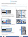
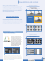
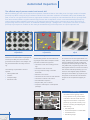
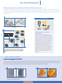
GE
Sensing & Inspection Technologies
A GUIDE TO
THE INSPECTION
AND ANALYSIS
OF ELECTRONIC PACKAGES
with phoenix|x-ray microfocus and nanofocus X-ray systems
FAQs about X-ray
How X-ray inspection
source
large FOD
works
object
FDD
detector
high magnification
low magnification
insulator
UH
cathode
(filament)
UG
UACC
grid
anode
magnetic
lens
electron beam
deflection
unit
X-ray starts with a sample being irradiated by an X-ray source and projected onto a
detector. The geometric magnification M of the image is the ratio of focus-detector
distance (FDD), Focus-object distance (FOD): M=FDD/FOD. The smaller the focal spot,
the greater the resolution. With the nanofocus technology a unique detail detectability down to 0.2 microns can be achieved. phoenix|x-ray systems reach geometric
magnifications over 2 000 x resulting in total magnifications beyond 24 000 x.
How X-ray tubes
What makes an excellent
work
X-ray?
The heart of the X-ray machine is an elec-
In addition to resolution, maximum voltage,
trode pair consisting of a cathode, the fila-
and power, stability is very important for
ment, and an anode, that is located inside a
reliable results and highest up-time. One of
vacuum tube. Current is passed through the
phoenix|x-ray’s key techno-logy competen-
filament heating it up, causing the filament
cies are tube design and manufacturing.
to emit electrons. The positively charged
target
anode draws the electrons across the tube.
X-ray beam
Unlike with conventional X-ray tubes, the
electrons pass through the anode into a specifically designed set-up of electromagnetic
lenses, where they are bundled and directed
Why can the collision
onto a small spot on the target, a flat metal
protection be deactivated?
the electrons collide with the target, they in-
disc covered by a layer of tungsten. When
0.50
dose rate variation [%]
small FOD
dose rate stability XS|160 T
0.25
0.5%
0.00
-0.25
-0.50
0
1
2
3
4
5
teract with the ions in the tungsten, causing
6
7
8
time [h]
phoenix|x-ray systems come standard with
X-rays to be emitted. Key to sharp, crisp
a password-protected, anti-collision feature
X-ray images at micron or even submicron
to ensure the protection of your samples.
to 180 kV and unipolar microfocus X-ray
resolutions is the size of the focal spot,
When inspecting certain samples, it might
tubes up to 300 kV maximum voltage
meaning the ability to focus the electron
become necessary to deactivate the collision
beam in such way that the area on the target
protection (e.g. with 25 μm bond wires, which,
where the electrons hit be as small as pos-
even for magnifications of just 500 x, need
sible – an obstacle yet to be overcome by
to be as close as 4 mm to the tube head).
conventional X-ray machines.
phoenix|x-ray provides the user the flexibility
However, phoenix|x-ray has mastered this
when dealing with small samples. Unlike
challenge with its unique nanofocus tube
with conventional systems, the X-ray tube is
during fabrication and automated warm-
providing detail detectabilities as low as 200
located above the sample tray allowing the
up procedures prevent discharges
nanometers (0.2 microns).
user to move the sample as close to the tube
head as needed.
• High power nanofocus X-ray tubes up
• Up to 200 nm (0.2 microns) detail detectability
• Dose-rate stabilization: the emitted
intensity only varies by less than 0.5 %
within 8 hours (see diagram)
• Anti-arcing: dedicated surface treatment
• Self adjustment: all tube adjustments are
performed automatically during warm-up
to achieve optimum results
• Plug-in cathodes: pre-adjusted spare cathodes prevent malfunction due to wrong
filament adjustment and minimize downtime to less than 20 min.
• Target check: target condition is checked
FOD = -4 mm: 500 x Sample touching the tube:
Maximum magnification
automatically; automatic target wear is
indicated
The View Inside
What can X-ray inspection tell us about package quality?
Electronic packages are sophisticated electronic devices with complex, internal features. In order to meet the quality requirements of the industry, X-ray inspection solutions must be capable of delivering detail detectabilities in the submicron range and
detecting hidden defect flaws.
phoenix|x-ray offers automated microfocus and nanofocus X-ray inspection solutions for any package inspection task including,
but not limited to the following:
Standard IC packages: DIP, SOT, VSOP, (P)LCC,
QFP, Flat Pack
Cracked wire Wire destroyed by overvoltage
>
>
IC-package, top-down view
Any internal details such as bond wires, inner and outer bonds, die,
die attach, lead frame and moulding can be examined for defects (e.g.
broken wires, excessive wire sweep, extraneous or crossing wires, die
attach voids and die tilt, die cracks, defective lid seals, moulding voids,
entrapped particles and delaminations).
Wedge-bond inspection Ball-bond inspection
Wire-bonded area array packages:
PBGA, CSP, etc.
>
>
>
>
Chip-scale package in top-down view (not balled yet)
Shape deviations and opens Bridge between flip-chip
in flip-chip bonds bonds
The image gives a clear view of the integrity of the vias and lead tracks of
the PCB and the quality of the solder joints.
Flip-chip bonded area array packages:
CBGA etc.
>
Die attach
voids
Cracked die
ting IC and ceramic substrate as well as underfill inspection. The most
common defects are open solder joints, missing solder joints, solder
bridges, solder and underfill voids.
>
Applications include the inspection of microscopic solder joints connec-
>
FC-bonded IC, top-down view
Image definition and contrast
What is it that makes the difference?
Image definition and contrast are both key to detecting. With
the nanofocus technology with detail detectabilities down
to 200 nanometers, submicron resolutions and a fully digital
high-contrast|detector that outperforms any image intensifierbased image chain, phoenix|x-ray is once more leading the
way in X-ray inspection technology.
Unrivaled resolutions
nanofocus technology
microfocus: microfocus:
Focal spot size 10 microns Focal spot size 5 microns
High dynamic digital detectors
active temperature stabilization
The image quality is essential for an optimal defect coverage
of all 2D and 3D inspection tasks. The new active temperature
stabilized GE DXR detectors ensure a very low noise live-imaging. Due to its high dynamic, the DXR detector shows a brilliant
live image with 30 frames per second at full resolution.
nanofocus
focal spot
< 1 micron
Flip-chip bonds, 30 microns in diameter
Technology
microfocus image F = 5 μm nanofocus image
What is the difference between
nanofocus and microfocus tubes?
Superior contrast
source
object
Microfocus X-ray tubes have focal
spots that are as small as 3 microns
in size. But penumbra effects, and,
high-contrast|detector
Non-conductive die attach
as a consequence, residual unsharpdetector
ness, still occur. With its nanofocus
technology with focal spot sizes well
microfocus system
nanofocus system
below 1 micron, phoenix|x-ray has
successfully managed to eliminate
the penumbra effect even when us-
high-contrast|detector image|intensifier
ing highest-intensity X-rays.
Test pattern (W on Si) with period 2 μm
Copper Wires
Focal spot 3 microns Focal spot 600 nm (0.6 microns)
Verification of resolution using a periodic test pattern. If the
grid period is the same size as the focal spot, the pattern vanishes. Using nanofocus technology, the bars are clearly visible
proving that nanofocus tubes deliver detail detectabilities well
below 1 micron – proved with Jima.
high-contrast|detectors enable inspection of low absorbing
features
Automated Inspection
The efficient way of process control and rework: AXI
Efficient soldering process control requires the acquisition of statistical data on the solder joints of a larger number of samples.
phoenix|x-ray offers a range of plug-in software modules for the automatic evaluation of standard solder joints like BGA, QFP,
QFN, or PTH. For non-typical interconnections, appropriate modules can quickly be customized with the XE² (X-ray image Evaluation Environment) software. Together with the high precision CNC manipulation, which comes standard with phoenix|x-ray
systems these modules enable the automatic X-ray inspection (AXI) of solder joints at minimum set-up time, due to teach-in
programming and auto-setup routines. An additional software package – quality|review – is the perfect connection to rework.
phoenix|x-ray's inspection modules can also easily be activated during manual inspection as a quick inspection aid.
c4|module
vc|module
x|act
flip-chip inspection
voiding calculations
AXI with highest defect coverage
Software for the automated X-ray analysis of
Software designed for the automated void-
As a solution for AXI with highest defect cov-
microscopic solder joints, even with back-
ing analysis of die-attach and planar solder
erage, phoenix|x-ray provides calibrated high
ground structures present. The analysis runs
joints with versatile set-up options:
precision offline AXI systems including the
fully automated and is extremely time-sav-
• Calculation of the total voiding percent-
unique x|act software package for fast and
ing.
The following c4-parameters can be in-
• Calculation of the void count
• Sorting voids according to variable
spected:
• Missing solder balls
• Void size
• Void percentage
• Number of voids
easy offline CAD-programming. Small views
age
•
•
•
•
•
•
with highest resolution of a few micrometers,
360° rotation and oblique viewing up to 70°
thresholds
ensure to meet highest quality standards.
Definition of hot zones
Among the automated X-ray inspection, the
Calculation of the minimum void diameter
AXI system can be used for manual failure
Calculation of die tilt and rotation
analysis or 3D computed tomography as
Automated die inspection
well.
Dimple solder joint correction
Inspection and analysis of multiple-die
packages
Technology
The radiation dose typically used in
X-ray inspection is only a thousandth
of the dose rate that would cause damage to semiconductor components.
phoenix|x-ray provides a variety of options for controlling and adjusting the
dose rate e.g.:
Multiple-die attach evaluation
•
•
•
•
low-dose|mode
automated inspection routines (AXI)
collimated beams
self-filtering target
The Third Dimension
Oblique or straight X-ray inspection seen from a different perspective
Sometimes when inspecting a sample, it may become necessary to see your sample from a different angle. An example of this
would be an inspection via platings or wire loops. phoenix|x-ray systems provide oblique views of up to 70 degrees using the
unique ovhm-technology. Automatic isocentric manipulator movement locks the field of view during rotation and ovhm tilt in the
image centre.
Examples
Technology
X-ray tube
Via inspection with Wire loop inspection with
ovhm ovhm
detector
0-70°
Conventional tilting vs. ovhm
CSP
ovhm: Oblique views at highest
magnifications
PCB
Conventional tilt techniques generate
70°
oblique views by simply tilting the sample
to the side, which involves moving one part
of the sample further away from the X-ray
45°
0°
tube resulting in a decrease in magnification. The ovhm|module was specifically
designed to enable oblique views of up to
70 degrees and 0 to 360 degree rotations without a decrease in magnification.
ovhm: oblique views are an excellent means for gaining a maximum of information about the internal features of a sample.
At a tilt angle of 70 degrees, the profile of CSP-solder joints including voids are clearly visible. Unlike with a tilting angle of
45 degrees, component and board parts can be clearly distinguished.
Magnification remains the same because
the distance between focus and sample
does not change while the detector is being tilted.
High-resolution 3D imaging
nanoCT®
The proven and successful v|tome|x technology by phoenix|x-ray is also available as an add-on for the nanome|x system. High-power nanofocus X-ray technology paired with a fast reconstruction software deliver unrivaled, highest-quality inspection results with nanoCT® image resolutions. This technology is especially suitable for the inspection and three-dimensional analysis of smaller samples.
2D
CT
>
>
2D images of a memory cube with stacked dies, frontal
and side view. Deeper-lying features are concealed,
making a thorough analysis impossible.
3D nanoCT®-image: Each individual die attach is clearly
visible and can be examined for voids.
Systems
phoenix|x-ray offers a wide range of X-ray systems in different configurations for a variety of inspection tasks in the electronics
and semiconductor industries. phoenix|x-ray’s systems have superior specifications that are able to solve the highest demands:
nanome|x
microme|x
the ultimate X-ray solution
automated solder joint inspection
This automated X-ray system with superior
specifications satisfies the highest demands:
The 180 kV / 15 W high-power nanofocus tube
(4-in-1) covers the full range from submicron
resolution to high intensity applications. Due to
the easy view configuration, the X-ray image
displays the sample exactly as the operator
sees it through the radiation protection window. The digital realtime image chain with
4 MPixel camera provides an excellent contrast
resolution and enables oblique views up to 70 degrees at magnifications well above
24 000 x. For samples of poor contrast the system may be equipped with a high
dynamic fully digital high-contrast|detector – as supplement to the image chain, offering unique performance and versatility. Optionally, the nanome|x may be equipped
with nanoCT® capability.
pcb|inspector
nanotom
high performance - low maintenance
highest resolution in three dimensions
pcb|inspector is the solution for
process control on standard BGA / SMD
and planar solder joints. Due to the
maintenance-free closed tube and
the high quality image chain the
pcba|inspector provides excellent defect
recognition at medium magnifications.
Optional manipulation upgrades enable
oblique views.
The nanotom® comes standard with a
180 kV / 15 W ultra high-performance
nanofocus tube and precision mechanics for maximum stability. With voxel
resolution as low as 500 nanometer, the
nanotom® is the inspection solution of
choice for 3D CT applications in a wide
range of fields. With its small footprint,
the nanotom is suitable for even the
smallest labs.
®
For many applications, the nanotom®
offers a viable alternative to synchrotron-based computed tomography.
The microme|x is a high-resolution
automated X-ray inspection (AXI) system
that is most suitable for failure analysis
in the semiconductor and electronics
industry. It comes standard with an ultra
high performance 180 kV / 20 W X-ray
tube for sub-micron feature recognition
> 0.5 μm and a high-resolution 2 MPixel
digital image chain. This system provides
a total magnification of up to 23.320x
(without software zoom) and oblique
angle views of up to 70 degrees. The
microme|x combines proven high-resolution 2D and 3D CT X-ray technology in
one system. With the new x|act package
for CAD based AXI programming the
microme|x is the system of choice to ensure meeting zero defect requirements.
Technology
Closed tube or open tube?
Closed tubes: All tube components
are contained in a sealed vacuum
vessel container. Closed tubes are
maintenance-free and are completely
replaced at the end of their lifetime.
Open tubes: All components and wearout parts are accessible and replaceable, the tube is continuously evacuated
by a turbomolecular pump. Open tubes
yield higher resolution and magnification and are not limited in lifetime.
Regional Contact Information
Europe, Asia, Africa, South America
GE Sensing & Inspection Technologies
Niels-Bohr-Str. 7
31515 Wunstorf
P.O. Box 6241
31510 Wunstorf
Germany
Tel.: +49 5031 172 0
Fax: +49 5031 172 299
E-mail: [email protected]
[email protected]
Americas
GE Sensing & Inspection Technologies
50 Industrial Park Road
Lewistown, PA 17044
USA
Tel: +1 (866) 243 2638 (toll-free)
Tel: +1 (717) 242 0327
E-mail: [email protected]
www.phoenix-xray.com
GEIT-31102EN (11/09)
© 2009 General Electric Company. All Rights Reserved. Specifications subject to change without prior notice. nanotom and nanoCT are registered trademarks of General Electric Company. Other company or product
names mentioned in this document may be trademarks or registered trademarks of their respective companies, which are not affiliated with GE.