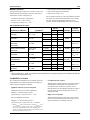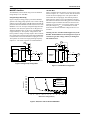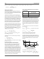
1
www.fairchildsemi.com Application Note 42 Implementing the RC5040 and RC5042 DC-DC Converters on Pentium® Pro Motherboards Introduction This document describes how to implement a switching voltage regulator using an RC5040 or an RC5042 high speed controller, a power inductor, a Schottky diode, appropriate capacitors, and external power MOSFETs. This regulator forms a step down DC-DC converter that can deliver up to 14.5A of continuous load current at voltages ranging from 2.1V to 3.5V. A specific application circuit, design considerations, component selection, PCB layout guidelines and performance evaluation procedures are covered in detail. In the past 10 years, microprocessors have evolved at such an exponential rate that a modern chip can rival the computing power of a mainframe computer. Such evolution has been possible because of the increasing numbers of transistors that processors integrate. Pentium CPUs, for example, integrate well over 5 million transistors on a single piece of silicon. To integrate so many transistors on a piece of silicon, their physical geometry has been reduced to the sub-micron level. As a result of each geometry reduction, the corresponding operational voltage for each transistor has also been reduced. This changing voltage for the CPU demands the design of a programmable power supply—a design that is not completely re-engineered with every change in CPU voltage. The operational voltage of CPUs has shown a downwards trend for the past 5 years: from 5V for the x386 and x486, to 3.3V for Pentium, and 3.1V for Pentium Pro. Furthermore, emerging chip technologies may require operating voltages as low as 2.5V. With this trend in mind, Raytheon Electronics has designed the RC5040 and RC5042 controllers. These controllers integrate the necessary programmability to address the changing power supply requirements of lower voltage CPUs. Previous generations of DC-DC converter controllers were designed with fixed output voltages adjustable only with a set of external resistors. In a high volume production environment (such as with personal computers), however, a CPU voltage change requires a CPU board re-design to accommodate the new voltage requirement. The integrated 4-bit DAC in the RC5040 and the RC5042 reads the voltage ID code from the Pentium Pro microprocessor and configures the system to provide the appropriate voltage. In this manner, the PC board does not have to be re-designed each time the CPU voltage changes. The CPU can thus automatically configure its own required voltage. Pentium Pro and OverDrive® Processor Power Requirements Use Intel’s AP-523 Application Note, Pentium® Pro Processor Power Distribution Guidelines, November 1995 (order number 242764-001), as a basic reference. The specifications contained in this document have been modified slightly from the original Intel document to include updated specifications for Pentium Pro microprocessors. Please contact Intel Corporation for specific details. Input Voltages Available inputs are +5V ±5% and +12V ±5%. Raytheon Electronics’ DC-DC converters may use either or both inputs. Their input voltage requirements are listed in Table 1. Table 1. Input Voltage Requirements Controller VCC MOSFET Drain MOSFET Gate Bias RC5040 RC5042 +5V ±5% +5V ±5% +5V ±5% or 12V ±5% RC5043 +5V ±5% 12V ±5% 12V ±5% Part # Pentium Pro DC Power Requirements Refer to Table 2 for the power supply specifications for Pentium Pro and Overdrive Processors. For a motherboard design without a standard Voltage Regulator Module (VRM) socket, the on-board DC-DC converter must supply a minimum ICCP current of 13.9A at 2.5V and 12.4A at 3.3V. For a flexible motherboard design, the on-board converter must be able to supply 14.5A maximum ICCP. DC Voltage Regulation As indicated in Table 2, the voltage level supplied to the CPU must be within ±5% of its nominal setting. Voltage regulation limits must include: • • • • Output load ranges specified in Table 2 Output ripple/noise DC output initial voltage set point Temperature and warm up drift (Ambient +10°C to +60°C at full load with a maximum rate of change of 5°C per 10 minutes minimum but no more than 10°C per hour) • Output load transient with: Slew rate >30A/µs at the converter pins Range: 0.3A – ICCP Max (as defined in Table 2). Rev. 1.1.0 AN42 APPLICATION NOTE Table 2. Intel Pentium Pro and OverDrive Processor Power Specifications CPU Model & Features Voltage Specification VCCP (VDC) Maximum Current ICCP (A) Maximum Thermal Design Power1 (W) 150MHz – 256K L2 Cache 3.1 ± 5% 9.9 29.2 166MHz – 512K L2 Cache 3.3 ± 5% 11.2 35.0 180MHz – 256K L2 Cache 3.3 ± 5% 10.1 31.7 200MHz – 256K L2 Cache 3.3 ± 5% 11.2 35.0 200MHz – 512K L2 Cache 3.3 ± 5% 12.4 37.9 2.5 ± 5% 11.2 26.7 12.5 29.7 13.9 32.9 14.5 45.0 OverDrive Processors 150 MHz 180 MHz 200 MHz Flexible Motherboard2 2.4-3.5 ± 5% Notes: 1. Maximum power values are measured at typical VCCP to take into account the thermal time constant of the CPU package. 2. Flexible motherboard specifications are recommendations only. Actual specifications are subject to change. Output Ripple and Noise Ripple and noise are defined as periodic or random signals over the frequency band of 20MHz at the output pins. Output ripple and noise requirements of ±1.0% must be met throughout the full load range and under all specified input voltage conditions. Efficiency The efficiency of the DC-DC converter must be greater than 80% at high current draw and greater than 40% at low current draw. Processor Voltage Identification The Pentium Pro package has four voltage identification pins, VID3–VID0, that can be used for automatic selection of the power supply voltage. These pins are internally unconnected or are shorted to ground (VSS). The logic status of the pins defines the voltage required by the processor. The VID codes have been implemented to support voltage specification variations on future Pentium Pro processors. These codes are presented in Table 3. A ‘1’ refers to an open pin and a ‘0’ refers to a short to ground. The VCCP power supply should supply the voltage that is requested or disable itself. Table 3. Voltage Identification Codes for Pentium Pro Data Bits VCCP VID3 VID2 VID1 VID0 (VDC) 1 1 1 1 No CPU 1 1 1 0 2.1 1 1 0 1 2.2 1 1 0 0 2.3 1 0 1 1 2.4 1 0 1 0 2.5 1 0 0 1 2.6 1 0 0 0 2.7 0 1 1 1 2.8 0 1 1 0 2.9 0 1 0 1 3.0 0 1 0 0 3.1 0 0 1 1 3.2 0 0 1 0 3.3 0 0 0 1 3.4 0 0 0 0 3.5 I/O Controls In addition to the voltage identification pins, several signals exist to control the DC-DC converter or to provide feedback from the converter to the CPU. These are Power-Good (PWRGD), Output Enable (OUTEN), and Upgrade Present (UP). These signals are discussed later. 2 APPLICATION NOTE AN42 RC5040 and RC5042 Description Simple Step-Down Converter S1 L1 + VIN D1 C1 RL Vout – 65-AP42-01 Figure 1. Simple Buck DC-DC Converter Figure 1 illustrates a step-down DC-DC converter with no feedback control. The basic step-down converter serves as the basis for deriving the design equations for the RC5040 and RC5042. From Figure 1, the basic operation begins by closing the switch S1, so that the input voltage VIN is impressed across inductor L1. The current flowing through this inductor is given by the following equation: ( V IN – V OUT )T ON I L = ----------------------------------------------L1 where TON is the duty cycle (the time when S1 is closed). When S1 opens, the diode D1 conducts the inductor current and the output current is delivered to the load according to the following equation: V OUT ( T S – T ON ) I L = -------------------------------------------L1 where TS is the overall switching period and (TS – TON) is the time during which S1 is open. By solving these equations you can obtain the basic relationship for the output voltage of a step-down converter: T ON V OUT = V IN ----------- TS In order to obtain a more accurate approximation for VOUT, we must also include the forward voltage VD across diode D1 and the switching loss, VSW. After taking into account these factors, the new relationship becomes: V OUT T ON = ( V IN + V D – V SW ) ----------- – V D TS Where VSW = IL • RDS,ON. The RC5040 and RC5042 Controllers The RC5040 is a programmable synchronous-mode DC-DC converter controller. The RC5042 is a non-synchronous version of the RC5040. When designed with the appropriate external components, either device can be configured to deliver more than 14.5A of output current. During heavy loading conditions, these controllers function as currentmode PWM step-down regulators. Under light loads, they function in PFM (pulse frequency modulation) or pulse skipping mode. The controllers sense the load level and switch between the two operating modes automatically, thus optimizing efficiency under all loads. The key differences between the RC5040 and RC5042 are listed in Table 4. Table 4. RC5040 and RC5042 Differences RC5040 RC5042 Operation Synchronous Non-Synchronous Package 20-pin SOIC 16-pin SOIC Yes No Output Enable/ Disable Refer to the RC5040 Block Diagram illustrated in Figure 2. The control loop of the regulator contains two main sections: the analog control block and the digital control block. The analog block consists of signal conditioning amplifiers feeding into a set of comparators which provide the inputs to the digital block. The signal conditioning section accepts inputs from the IFB (current feedback) and VFB (voltage feedback) pins and sets two controlling signal paths. The voltage control path amplifies the VFB signal and presents the output to one of the summing amplifier inputs. The current control path takes the difference between the IFB and VFB and presents the result to another input of the summing amplifier. These two signals are then summed together with the slope compensation input from the oscillator. This output is then presented to a comparator, which provides the main PWM control signal to the digital control block. The additional comparators in the analog control section sets the threshold for when the RC5040 enters PFM mode during light loads and the point when the current limit comparator disables the output drive signals to the MOSFETs. The digital control block is designed to take the comparator inputs along with the main clock signal from the oscillator and provide the appropriate pulses to the HIDRV and LODRV pins that control the external power MOSFETs. The digital section was designed utilizing high speed Schottky transistor logic, thus allowing the RC5040 to operate at clock speeds as high as 1MHz. 3 AN42 APPLICATION NOTE Main Control Loop RC5040 +5V VIN OSCILLATOR – + – + – + 4-BIT DAC VREF – + VO DIGITAL CONTROL 1.24V REFERENCE POWER GOOD PWRGD 65-5040-01 VID0 VID1 VID2 VID3 Figure 2. RC5040 Block Diagram High Current Output Drivers Power Good (PWRGD) The RC5040 contains two identical high current output drivers that use high speed bipolar transistors in a push-pull configuration. Each driver is capable of delivering 1A of current in less than 100ns. Each driver’s power and ground are separated from the chip power and ground for additional switching noise immunity. The HIDRV driver’s power supply, VCCQP, is boot-strapped from a flying capacitor as illustrated in Figure 3. Using this configuration, C12 is charged from VCC via the Schottky diode DS2 and boosted when the FET is turned on. This scheme provides a VCCQP voltage equal to 2•VCC – VDS(DS2), or approximately 9.5V when VCC = 5V. This voltage is sufficient to provide the 9V gate drive to the MOSFET that is required to achieve a low RDS(ON). Since the low side synchronous FET is referenced to ground (see Figure 4), boosting the gate drive voltage is not needed and the VCCP power pin can be tied to VCC. Refer to Typical Operating Characteristics of the RC5040 data sheet for a full load VCCQP waveform. The RC5040 and RC5042 Power Good function has been designed according to Intel’s Pentium Pro DC-DC converter specification. The Power Good function provides a constant voltage monitor on the VFB pin. The internal circuitry of the converter compares the VFB signal to the VREF voltage and outputs an active-low interrupt signal to the CPU when the power supply voltage exceeds ±7% of its nominal setpoint. The Power Good flag provides no other control function to the RC5040. Internal Voltage Reference The reference used in the RC5040 is a precision band-gap voltage reference, with internal resistors precisely trimmed to provide a near zero temperature coefficient, TC. Added to the reference voltage is the output from a 4-bit DAC. The DAC is provided meet Pentium Pro specifications, requiring a programmable converter output via a 4-bit voltage identification (VID) code. This code scales the output voltage from 2.0V (no CPU) to 3.5V in 100mV increments. To guarantee stable operation under all loads, a 10KΩ pull-up resistor and 0.1µF of decoupling capacitance should be connected to the VREF pin. No load should be imposed on this pin. 4 Output Enable (OUTEN) Intel specifications state that the DC-DC converter should accept an open collector signal for controlling the output voltage. A logic LOW for this signal disables the output voltage. When disabled, the PWRGD output is in the low state. This feature is available for the RC5040 only. Upgrade Present (UP#) Intel specifications state that the DC-DC converter must accept an open collector signal that indicates the presence of an upgrade processor. The typical state is high (for a standard P6 processor). When the signal is low or in theground state (for the OverDrive processor), the output voltage must be disabled unless the converter can supply the OverDrive processor’s power requirements. When disabled, the PWRGD output must be in the low state. Because the RC5040 and RC5042 can supply the OverDrive processor requirements, the UP# signal is not required. APPLICATION NOTE AN42 Over-Voltage Protection The RC5040 and RC5042 constantly monitor the output voltage for protection against over voltage. If the voltage at the VFB pin exceeds 20% of the selected program voltage, an over-voltage condition is assumed, and the controller disables the output drive signal to the external MOSFET(s). Short Circuit Protection A current sense methodology is implemented to disable the output drive signal to the MOSFET(s) when an over-current condition is detected. The voltage drop created by the output current flowing across a sense resistor is presented to an internal comparator. When the voltage developed across the sense resistor exceeds the comparator threshold voltage, the controller disables the output drive signal to the MOSFET(s). In general, a lower operating frequency increases the peak ripple current flowing through the output inductor, allowing the use of a larger inductor value. Operation at lower frequencies increases the amount of energy storage that the bulk output capacitors must provide during load transients that occur due to the slower loop response of the controller. In addition, note that the efficiency losses due to switching are relatively fixed per switching cycle. Therefore, as the switching frequency increases, the contribution toward efficiency due to switching losses also increases. RC5040 has an optimal operating frequency of 650KHz. This frequency allows the use of smaller inductive and capacitive components while optimizing peak efficiency under all operating conditions. Design Considerations and Component Selection The DC-DC converter returns to normal operation after the fault has been removed, for either an over voltage or a short circuit condition. Application Circuits Oscillator The RC5040 oscillator section is implemented using a fixed current capacitor charging configuration. An external capacitor (CEXT) is used to preset the oscillator frequency between 200KHz and 1MHz. This allows maximum flexibility in setting the switching frequency and in choosing external components. Figure 3 illustrates a typical non-synchronous application using the RC5040. Figure 4 shows a typical synchronous application using the RC5040, and Figure 5 shows a typical non-synchronous application using the RC5042. L2 C5 0.1µF DS2 C8 C9 0.1µF 0.1µF 1N5817 M1 13 14 15 R7 10K 16 VREF RC5040 0.1µF GND 1µF 7 6 5 2SK1388 L1 1.3µH C6 4.7µF 4 3 2 1 17 18 19 20 C7 M2 2SK1388 C12 10 9 8 DS1 MBR1545CT RSENSE 8mΩ 1500µF 11 12 C15 C3 C2 1000µF 1000µF 1000µF 1500µF C1 0.1µF 1500µF C4 C14 2.6µH C13 VCC VO CEXT 39pF VID3 VID2 VID1 VID0 R1 10K R2 10K R3 10K R4 10K VCC R6 10K PWRGD VCC 65-AP42-03 C11 0.22µF R5 OUTEN C10 0.1µF 10K Figure 3. Non-Synchronous DC-DC Converter Application Schematic Using RC5040 5 AN42 APPLICATION NOTE L2 VCC C5 0.1µF C8 C9 0.1µF 0.1µF M1 12 13 14 15 R7 10K 16 17 VREF C7 0.1µF GND M2 2SK1388 C12 10 9 1µF 8 2SK1388 L1 7 RC5040 C6 6 5 3 19 20 2 1 8mΩ 4.7µF 4 18 RSENSE 1.3µH M3 1500µF 11 1500µF DS2 1N5817 C15 C3 1000µF 1000µF 1500µF C2 1000µF C14 C1 0.1µF C13 2.6µH C4 VO DS1 2SK1388 1N5817 CEXT 39pF VID3 VID2 VID1 VID0 R1 10K R2 10K R3 10K R4 10K VCC R6 10K PWRGD 65-AP42-04 C11 0.22µF VCC R5 OUTEN 10K C10 0.1µF Figure 4. Synchronous DC-DC Converter Application Schematic Using RC5040 L2 C5 0.1µF DS2 1N5817 C8 C9 0.1µF 0.1µF M2 2SK1388 C12 R7 10K VREF 8 10 7 11 12 6 5 4 3 13 14 C7 0.1µF GND RC5042 15 16 M1 2SK1388 L1 1.3µH C6 4.7µF RSENSE 8mΩ 1500µF 1µF 9 C15 1000µF 1000µF 1000µF 1500µ F C3 C2 1500µF C1 0.1µF C13 C4 2.6µH C14 VCC DS1 MBR1545CT 2 1 CEXT 39pF VID3 VID2 VID1 VID0 R1 10K R2 10K R3 10K R4 10K VCC C10 0.1µF R6 10K 65-AP42-05 PWRGD VCC C11 0.22µF Figure 5. Non-Synchronous DC-DC Converter Application Schematic Using RC5042 6 VO APPLICATION NOTE AN42 MOSFET Selection This application requires the use of N-channel, Logic Level Enhancement Mode Field Effect Transistors. The desired characteristics of these components are: • Low Static Drain-Source On-Resistance RDS,ON < 37 mΩ (lower is better) • Low gate drive voltage, VGS ≤ 4.5V • Power package with low thermal resistance • Drain current rating of 20A minimum • Drain-Source voltage > 15V. The on-resistance (RDS,ON) is the main parameter for MOSFET selection. It determines the MOSFET’s power dissipation, thus significantly affecting the efficiency of the converter. Several suitable MOSFETs are shown in Table 5. Table 5. MOSFET Selection Table RDS, ON (mΩ) 1 Manufacturer & Model # Conditions Fuji 2SK1388 VGS = 4V ID = 17.5A Siliconix SI4410DY VGS = 4.5V ID = 5A National Semiconductor NDP706AL VGS = 5V ID = 40A NDP706AEL National Semiconductor NDP603AL National Semiconductor NDP606AL Motorola MTB75N03HDL Int. Rectifier IRLZ44 Int. Rectifier IRL3103S VGS = 4.5V ID = 10A TJ = 25°C Typ. Max. Package Thermal Resistance 25 37 TO-220 ΦJA = 75 ΦJA = 50 TJ = 125°C 37 — TJ = 25°C 16.5 20 TJ = 125°C 28 34 SO-8 (SMD) TJ = 25°C 13 15 TO-220 ΦJA = 62.5 ΦJC = 1.5 TJ = 125°C 20 24 TJ = 25°C 31 40 TO-220 ΦJA = 62.5 TJ = 125°C 42 54 ΦJC = 2.5 TJ = 25°C 22 25 TJ = 125°C 33 40 VGS = 5V ID = 37.5A TJ = 25°C 6 9 TO-263 ΦJA = 62.5 TJ = 125°C 9.3 14 (D2 PAK) ΦJC = 1.0 TJ = 25°C — 28 TO-220 ΦJA = 62.5 TJ = 125°C — 46 TJ = 25°C — 19 VGS = 5V ID = 31A VGS = 4.5V ID = 28A TJ = 125°C TO-220 ΦJA = 62.5 VGS = 5V ID = 24A ΦJC = 1.5 ΦJC = 1.0 TO-220 31 ΦJA = 62.5 ΦJC = 1.0 Note: 1. RDS(ON) values at Tj = 125°C for most devices were extrapolated from the typical operating curves supplied by the manufacturers and are approximations only. Two MOSFETs in Parallel We recommend two MOSFETs used in parallel instead of a single MOSFET. The following significant advantages are realized using two MOSFETs in parallel: • Significant reduction of power dissipation. Maximum current of 14A with one MOSFET: PMOSFET = (I2 RDS,ON)(Duty Cycle) = (14)2(0.050*)(3.3+0.4)/(5+0.4-0.35) = 7.2 W With two MOSFETs in parallel: PMOSFET = (I2 RDS,ON)(Duty Cycle) = (14/2)2(0.037*)(3.3+0.4)/(5+0.4-0.35) = 1.3W/FET • No added heat sink required. With the power dissipation down to around one watt and with MOSFETs mounted flat on the motherboard, no external heat sink is required. The junction-to-case thermal resistance for the MOSFET package (TO-220) is typically at 2°C/W and the motherboard serves as an excellent heat sink. • Higher current capability. With thermal management under control, this on-board DC-DC converter can deliver load currents up to 14.5A with no performance or reliability concerns. * Note: RDS,ON increases with temperature. Assume RDS,ON = 25mΩ at 25°C. RDS,ON can easily increase to 50mΩ at high temperature when using a single MOSFET. When using two MOSFETs in parallel, the temperature effects should not cause the RDS,ON to rise above the listed maximum value of 37mΩ. 7 AN42 APPLICATION NOTE MOSFET Gate Bias 12V Gate Bias The MOSFET(s) can be biased using one of two methods: Charge Pump or 12V Gate Bias. Figure 7 illustrates how an external 12V source can be used to bias VCCQP. A 47 Ω resistor is used to limit the transient current into the VCCQP pin, and a 1µF capacitor filter is used to filter the VCCQP supply. This method provides a higher gate bias voltage (VGS) to the MOSFET, and therefore reduces the RDS,ON and resulting power loss within the MOSFET. Figure 8 illustrates how RDS,ON decreases dramatically as VGS increases. A 6.2V Zener (DS2) is used to clamp the voltage at VCCQP to a maximum of 12V and ensure that the absolute maximum voltage of the IC is not exceeded. Charge Pump (or Bootstrap) Figure 6 employs a charge pump to provide the MOSFET gate bias. The charge pump capacitor, CP, is used as a flying capacitor to boost the voltage of the RC5040 or RC5042 output driver. When the MOSFET switches off, the source of the MOSFET is at -0.6V. VCCQP is charged through the Schottky diode to 4.5V. Thus, the capacitor CP is charged to 5V. When the MOSFET turns on, the source of the MOSFET is at approximately 5V. The capacitor voltage follows, and hence provides a voltage at VCCQP equal to 10V. The Schottky is required to provide the charge path when the MOSFET is off, and then reverses bias when the VCCQP goes to 10V. The capacitor CP needs to be a high Q and high frequency capacitor. A 1µF ceramic capacitor is recommended here. Warning: The 12V Gate Bias method applies only to the RC5042. The RC5040 has not been designed to accept an external 12V gate bias voltage, and may be damaged if this method is used. +5V +5V 47Ω +12V DS2 VCCQP D1 6.2V VCCQP M1 M1 HIDRV HIDRV CP L1 RS L1 VO PWM/PFM Control CB DS1 RS VO PWM/PFM Control DS1 CB 65-AP42-06 65-AP42-07 Figure 6. Charge Pump Configuration RDS,ON (Ω) Figure 7. 12V Gate Bias Configuration 0.1 0.09 0.08 0.07 0.06 0.05 0.04 0.03 0.02 0.01 0 R(DS)Fuji R(DS)Fuji R(DS)706A R(DS)-706AEL 1.5 2 2.5 3 3.5 4 5 6 7 8 9 Gate-Source Voltage, VGS (V) Figure 8. RDS,ON vs. VGS for Selected MOSFETs 8 10 11 APPLICATION NOTE AN42 Converter Efficiency Losses due to parasitic resistance in the switches, inductor, and sense resistor dominate at high load-current levels. The major loss mechanisms under heavy loads, in order of importance, are: • MOSFET I2R Losses • Inductor Losses • • • • • • Sense Resistor Losses Gate-Charge Losses Diode-Conduction Losses Transition Losses Input Capacitor Losses Losses Due to the Operating Supply Current of the IC. Efficiency of the converter under heavy loads can be calculated as follows: P OUT I OUT × V OUT Efficiency = -------------- = --------------------------------------------------------- , p IN I OUT × V OUT + P LOSS where PLOSS = PD MOSFET + PD INDUCTOR + PD RSENSE + PD GATE + PD DIODE + PD TRAN + PD CAP + PD IC Design Equations: V OUT + V D 2 (1) PD MOSFET = I OUT × R DS,ON × DutyCycle , where DutyCycle = -----------------------------------------V IN + V D – V SW 2 (2) PDINDUCTOR = I OUT × R INDUCTOR 2 (3) PD RSENSE = I OUT × R SENSE (4) PD GATE = q GATE × f × 5V , where qGATE is the gate charge and f is the switching frequency (5) PD DIODE = V f × I D ( 1 – DutyCycle ) 2 V IN × C RSS × I LOAD × f = ------------------------------------------------------------- , where CRSS is the reverse transfer capacitance of the high-side MOSFET. I DRIVE (6) PD TRAN 2 (7) PD CAP = I RMS × ESR (8) PD IC = V CC × I CC Example: 3.3 + 0.5 DutyCycle = ------------------------------ = 0.73 5 + 0.5 – 0.3 2 PDMOSFET = 10 × 0.030 × 0.73 = 2.19W 2 PD INDUCTOR = 10 × 0.010 = 1W 2 PD RSENSE = 10 × 0.0065 = 0.65W PD GATE = CV × f × 5V = 1.75nf × ( 9 – 1 )V × 650Khz × 5V = 0.045W PD DIODE = 0.5 × 10 ( 1 – 0.73 ) = 1.35W 2 5 × 400pf × 10 × 650khz PD TRAN = ---------------------------------------------------------------- ∼ 0.010W 0.7A 2 PDCAP = ( 7.5 – 2.5 ) × 0.015 = 0.37W PD IC = 0.2W 9 AN42 APPLICATION NOTE PDLOSS = 2.19W + 1.0W + 0.65W + 0.045W + 1.35W + 0.010W + 0.37W + 0.2W = 5.815W 3.3 × 10 ∴ Efficiency = --------------------------------------- ≈ 85% 3.3 × 10 + 5.815 Selecting the Inductor Selecting the right inductor component is critical in the DC-DC converter application. The inductor’s critical parameters to consider are inductance (L), maximum DC current (IO), and coil resistance (Rl). The inductor core material is crucial in determining the amount of current it can withstand. As with all engineering designs, tradeoffs exist between various types of core materials. In general, Ferrites are popular due to their low cost, low EMI properties, and high frequency (>500KHz) characteristics. Molypermalloy powder (MPP) materials exhibit good saturation characteristics, low EMI, and low hysteresis losses; however, they tend to be expensive and more effectively utilized at operating frequencies below 400KHz. Another critical parameter is the DC winding resistance of the inductor. This value should typically be as low as possible because the power loss in DC resistance degrades the efficiency of the converter by PLOSS = IO2 x Rl. The value of the inductor is a function of the oscillator duty cycle (TON) and the maximum inductor current (IPK). IPK can be calculated from the relationship: I PK V IN – V SW – V D = I MIN + ------------------------------------------ TON L Where TON is the maximum duty cycle and VD is the forward voltage of diode DS1. The inductor value can be calculated using the following relationship: V IN – V SW – V O L = ------------------------------------------ TON I PK – I MIN Table 6. RC5040 and RC5042 Short Circuit Comparator Threshold Voltage Short Circuit Comparator Vthreshold (mV) Typical 120 Minimum 100 Maximum 140 When designing the external current sense circuitry, pay careful attention to the output limitations during normal operation and during a fault condition. If the short circuit protection threshold current is set too low, the converter may not be able to continuously deliver the maximum CPU load current. If the threshold level is too high, the output driver may not be disabled at a safe limit and the resulting power dissipation within the MOSFET(s) may rise to destructive levels. The design equation used to set the short circuit threshold limit is as follows: V th R SENSE = --------, where: I SC = output short circuit current I SC ( I pk – I min ) I SC ≥ I inductor = I Load, max + ---------------------------2 where Ipk and Imin are peak ripple currents and Iload, max is the maximum output load current. You must also take into account the current (Ipk –Imin), or the ripple current flowing through the inductor under normal operation. Figure 9 illustrates the inductor current waveform for the RC5040 and RC5042 DC-DC converters at maximum load. I pk Where VSW (RDS,ON x IO) is the drain-to-source voltage of M1 when it is turned on. I (Ipk – I min )/2 Implementing Short Circuit Protection Intel currently requires all power supply manufacturers to provide continuous protection against short circuit conditions that may damage the CPU. To address this requirement, Raytheon Electronics has implemented a current sense methodology on the RC5040 and RC5042 controllers. This methodology limits the power delivered to the load during an overcurrent condition. The voltage drop created by the output current flowing across a sense resistor is presented to one terminal of an internal comparator with hysterisis. The other comparator terminal has a threshold voltage, nominally 120mV. Table 6 states the limits for the comparator threshold of the switching regulator: 10 ILOAD, MAX Imin TON TOFF t T = 1/fs Figure 9. Typical DC-DC Converter Inductor Current Waveform The calculation of this ripple current is as follows: ( VOUT + VD ) ( I pk – I min ) ( VIN –VSW – VOUT ) ---------------------------- = ------------------------------------------------- × ---------------------------------------------T ( VIN – VSW + VD ) L 2 APPLICATION NOTE AN42 where: • • • • VIN = Input Voltage to the Converter VSW = Voltage Across the MOSFET = ILOAD x RDS,ON VD = Forward Voltage of the Schottky Diode T = The Switching Period of the Converter = 1/fS, Where fS = Switching Frequency. For an input voltage of 5V, an output voltage of 3.3V, an inductor value of 1.3µH, and a switching frequency of 650KHz (using CEXT = 39pF), the inductor current can be calculated as follows: ( I PK – I min ) - = 14.5 + 1 = 15.5A I SC ≥ I inductor = I Load, max + ---------------------------2 For continuous operation at 14.5A, the short circuit detection threshold must be at least 15.5A. The next step is to determine the value of the sense resistor. Including tolerance, the sense resistor value can be approximated as follows: V th,min V th,min R SENSE = ---------------- × ( 1 – TF ) = ----------------------------------- × ( 1 – TF ) I SC 1.0 + I Load,max where TF = Tolerance Factor for the sense resistor. ( I pk – I min ) ( 5.0 – 14.5 × 0.037 – 3.3 ) -× ---------------------------- = ------------------------------------------------------------–6 2 1.3 × 10 ( 3.3 + 0.5 ) 1 -------------------------------------------------------------- × ----------------------- = 1.048A ( 5.0 – 14.5 × 0.037 + 0.5 ) 650 × 103 Several different types of sense resistors exist. Table 7 describes tolerance, size, power capability, temperature coefficient and cost of various sense resistors. Therefore, for a continued load current of 14.5A, the peak current through the inductor, Ipk, is found to be: Table 7. Comparison of Sense Resistors Description Motherboard Trace Resistor Tolerance Factor (TF) ±29% Size (L x W x H) 2" x 0.2" x 0.001" (1 oz Cu trace) Power capability Discrete Metal Discrete Iron Strip Surface Alloy Mount Resistor Resistor (IRC) (Dale) ±5% (±1% available) ±1% 0.45" x 0.065" x 0.25" x 0.125" x 0.200" 0.025" Discrete MnCu Alloy Wire Resistor Discrete CuNi Alloy Wire Resistor (Copel) ±10% ±10% 0.200" x 0.04" x 0.160" 0.200" x 0.04" x 0.100" > 50A/in 1 watt (3W and 5W available) 1 watt 1 watt 1 watt Temperature Coefficient +4,000 ppm +30 ppm ±75 ppm ±30 ppm ±20 ppm Cost @10,000 piece Low included in motherboard $0.31 $0.47 $0.09 $0.09 Refer to Appendix A for Directory of component suppliers Based on the Tolerance in the above table, for embedded PC trace resistor and for Iload,max = 14.5A: V th,min R SENSE = ----------------------------------------- × ( 1 – TF ) = 1.0A + I Load, max 100mV --------------------------------- × ( 1 – 29% ) = 4.6mΩ 1.0A + 14.5A For a discrete resistor and Iload, max = 14.5A: V th,min RSENSE = ----------------------------------------- × ( 1 – TF ) = 1.0A + I Load, max 100mV --------------------------------- × ( 1 – 5% ) = 6.1mΩ 1.0A + 14.5A For user convenience, Table 8 lists the recommended values for sense resistor at various load currents using an embedded PC trace resistor or discrete resistor. 11 AN42 APPLICATION NOTE Table 8. Rsense for various load currents Table 9 is a summary of tolerances for the Embedded PC Trace Resistor. ILoad,max (A) RSENSE PC Trace Resistor (mΩ) RSENSE Discrete Resistor (mΩ) 10.0 6.5 8.6 Tolerance due to sheet resistivity variation 16% 11.2 5.8 7.8 Tolerance due to L/W error 1% 12.4 5.3 7.1 Tolerance due to temperature variation 12% 13.9 4.8 6.4 Total Tolerance for PC Trace Resistor 29% 14.0 4.7 6.3 Design rules for using an embedded resistor 14.5 4.6 6.1 The basic equation for laying an embedded resistor is: Table 9. Summary PC Trace Resistor Tolerance L Discrete Sense Resistor L R = ρ × ------------W×t Discrete iron alloy resistors come in a variety of tolerances and power ratings, and are ideal for precision implementations. Either an MnCu alloy wire resistor or an CuNi alloy wire resistor is ideal for a low cost implementation. where ρ is the Resistivity (W-mil), L is the Length (mils), W is the Width (mils), and t is the Thickness (mils). For 1oz copper, t = 1.35 mils, ρ = 717.86 µΩ-mil, 1 L/1 W = 1 Square ( ■ ). Embedded Sense Resistor (PC Trace Resistor) For example, you can layout a 5.30mΩ embedded sense resistor. From Equations above, Embedded PC trace resistors have the advantage of almost zero cost implementation. However, the value of the PC trace resistors have large variations. Embedded resistors have 3 major error sources: the sheet resistivity of the inner layer, the mismatch due to L/W, and the temperature variation of the resistor. When laying out embedded sense resistors, consider all error sources described as follows: • Sheet resistivity. For 1 ounce copper, the thickness variation is typically between 1.15 mil and 1.35 mil. Therefore, the error due to sheet resistivity is (1.35 – 1.15)/1.25 = 16%. • Mismatch due to L/W. The error in L/W is dictated by the geometry and the power dissipation capability of the sense resistor. The sense resistor must be able to handle the load current and, therefore, requires a minimum width, calculated as follows: IL W = ---------0.05 where W is the minimum width required for proper power dissipation (mils), and IL is the load current in Amps. For a load current of 15A, the minimum width required is 300mils, which reflects a 1% L/W error. • Thermal Considerations. The I2R power losses cause the surface temperature of the resistor to increase along with its resistance value. In addition, ambient temperature variations add the change in resistor value: R = R 20 [ 1 + α 20 ( T – 20 )] where R20 is the resistance at 20°C, α20 = 0.00393/ °C,T is the operating temperature, andR is the desired value. For temperature T = 50°C, the %R change = 12%. 12 W t IL 10 W = ---------- = ---------- = 200mil 0.05 0.05 R×W×t 0.00530 × 200 × 1.35 L = ----------------------- = --------------------------------------------------- = 2000mi ρ 717.86 L/W = 10 ■. Therefore, to model 5.30mΩ enbedded resistor, you need W = 200 mils, and L = 2000 mils. See Figure 10. 1 1 1 1 1 1 1 1 1 1 W = 200 mils L = 2000 Figure 10. 5.30mΩ Sense Resistor (10 ■ ) You can also implement the sense resistor in the following manner. Each corner square is counted as 0.6 square since the current flowing through the corner square does not flow uniformly, concentrated towards the inside edge. This is shown in Figure 11. 1 1 1 1 1 1 .6 .6 1 1 .8 Figure 11. 5.30mΩ Sense Resistor (10 ■) A Resign Example Combining an Embedded Resistor with a Discrete Resistor For low cost implementation, the embedded PC trace resistor is the most desirable alternative, but, as discussed earlier, the wide tolerance (±29%) presents a challenge. In addition, changing CPU requirements may force the maximum load APPLICATION NOTE AN42 Embedded Sense Resistor IFBH MnCu Discrete Resistor R21 R22 IFBL Output Power Plane (Vout) R-∆r R R+∆r Figure 12. Short Circuit Sense Resistor Design Using PC Trace Resistor and Optional Discrete Sense Resistor currents to change. Therefore, combining an embedded resistor with a discrete resistor may be a desirable option. This section discusses a design that provides flexibility and addresses wide tolerances. Refer to Figure 12. In this design, the user has the option to choose either an embedded or a discrete MnCu sense resistor. To use the discrete sense resistor, populate R21 with a shorting bar (zero Ohm resistor) for a proper Kelvin connection and add the MnCu sense resistor. To use the embedded sense resistor, populate R22 with a shorting bar for a Kelvin connection. The embedded sense resistor allows you to choose a plus or a minus delta resistance tap to offset any large sheet resistivity change. In this design, the center tap yields 6mΩ, and the left or the right tap yield 6.7 or 5.3 mΩ, respectively. RC5040 and RC5042 Short Circuit Current Characteristics The RC5040 and RC5042 have a short circuit current characteristic that includes a hysteresis function. This function prevents the DC-DC converter from oscillating in the event of a short circuit. Figure 13 shows the typical characteristic of the DC-DC converter using a 6.5 mΩ sense resistor. 3.5 Power Dissipation Consideration During a Short Circuit Condition The RC5040 and RC5042 controllers respond to an output short circuit by drastically changing the duty cycle of the gate drive signal to the power MOSFET. In doing this, the power MOSFET is protected from over-stress and eventual destruction. Figure 14A shows the gate drive signal of a typical RC5040 operating in continuous mode with a load current of 10A. The duty cycle is then set by the ratio of the input voltage to the output voltage. If the input voltage is 5V and the output voltage is 3.1V, the ratio of Vout/ Vin is 62%. Figure 14B shows the result of the RC5040 going into its short circuit mode when the duty cycle is around 20%. Calculating the power on the MOSFET at each condition on the graph in Figure 13 shows how the protection scheme works. The power dissipated in the MOSFET at normal operation for a load current of 14.5A, is given by: 2.5 14.5 2˙ 2 P D = I × R ON × DutyCycle = ---------- × .037 × .62 = 1.2W 2 2.0 for each MOSFET. 3.0 Output Voltage The converter exhibits at normal load regulation until the voltage across the resistor reaches the internal short circuit threshold of 120mV. At this point, the internal comparator trips and signals the controller to turn off the gate drive to the power MOSFET. This causes a drastic reduction in the output voltage as the load regulation collapses into the short circuit control mode. The output voltage does not return to its nominal value until the output short circuit current is reduced to within the safe range for the DCDC converter. 1.5 The power dissipated in the MOSFET at short circuit condition for a peak short current of 20A, is given by: 1.0 0.5 0 0 5 10 15 20 25 Output Current Figure 13. RC5040/RC5042 Short Circuit Characteristic 20 2 P D = ------ × .037 × .2 = 0.74W 2 for each MOSFET. Thus, the MOSFET is not being over-stressed during a short circuit condition. 13 AN42 APPLICATION NOTE P D, Diode = I F, ave × V F × ( 1 – DutyCycle ) = 14 × 0.45 × 0.8 ≈ 5W Thus for the Schottky diode, the thermal dissipation during a short circuit is greatly magnified and requires that the thermal dissipation of the diode be properly managed by the appropriate choice of a heat sink. In order to protect the Schottky from being destroyed in the event of a short, we should limit the junction temperature to less than 130°C. Using the equation for maximum junction temperature, we can arrive at the thermal resistance required below: Figure 14A. VCCQP Output Waveform for Normal Operation Condition with Vout = 3.3V@10A T J ( max ) – T A P D = -------------------------------R ΘJA Assuming that the ambient temperature is 50°C, we get: T J ( max ) – T A 130 – 50 RΘJA = -------------------------------- = --------------------- = 16°C ⁄ W PD 5 Thus we need to provide for a heat sink that will give the Schottky diode a thermal resistance of at least 16°C/W or lower in order to protect the device during an indefinite short. In summary, with proper heat sink, the Schottky diode is not being over stressed during a short circuit condition. Schottky Diode Selection Figure 14B. VCCQP Output Waveform for Output Shorted to Ground The Schottky diode has a power dissipation consideration during the short circuit condition. During normal operation, the diode dissipates power when the power MOSFET is off. The power dissipation is given by: P D, Diode = I F × V F × ( 1 – DutyCycle ) = 14.5 × 0.5V × ( 1 – 0.62 ) = 2.75W In short circuit mode, the duty cycle is dramatically reduced to approximately 20%. The forward current during a short circuit condition decays exponentially through the inductor. The power dissipated on the diode during the short circuit condition, is approximated by: I F, ending = I sc × e 1 – ----------L⁄R = 20A × e I F, ave ≈ ( 20A + 7.9A ) ⁄ 2 ≈ 14A 14 1.5us – ------------1.3us ≈ 7.9A The application circuits of Figures 3, 4, and 5 show two Schottky diodes, DS1 and DS2. In synchronous mode, DS1 is used in parallel with M3 to prevent the lossy diode in the FET from turning on. In non-synchronous mode, DS1 is used as a flyback diode to provide a constant current path for the inductor when M1 is turned off. The Schottky diode DS2 serves a dual purpose. As configured in Figures 3, 4, and 5, DS2 allows the VCCQP pin on the RC5040 to be bootstrapped up to 9V using capacitor C12. When the lower MOSFET M3 is turned on, one side of capacitor C12 is connected to ground while the other side of the capacitor is being charged up to voltage VIN – VD through DS2. The voltage that is then applied to the gate of the MOSFET is VCCQP – VSAT, or typically around 9V. DS2 also provides correct sequencing of the various supply voltages by assuring that VCCQP is not enabled before the other supplies. A vital selection criteria for DS1 and DS2 is that they exhibit a very low forward voltage drop, as this parameter can directly affect the regulator efficiency. Table 10 lists several suitable Schottky diodes. Note that the MBR2015CTL has a very low forward voltage drop. This diode is ideal for applications where output voltages less than 2.8V are required. APPLICATION NOTE AN42 Table 10. Schottky Diode Selection Table Manufacturer Model # Conditions Forward Voltage VF Philips PBYR1035 IF = 20A; Tj=25°C IF = 20A; Tj=125°C < 0.84v < 0.72v Motorola MBR2035CT IF = 20A; Tj=25°C IF = 20A; Tj=125°C < 0.84v < 0.72v Motorola MBR1545CT IF = 15A; Tj=25°C IF = 15A; Tj=125°C < 0.84v < 0.72v Motorola IF = 20A; Tj=25°C MBR2015CTL IF = 20A; Tj=150°C < 0.58v < 0.48v Output Filter Capacitors Output ripple performance and transient response are functions of the filter capacitors. Since the 5V supply of a PC motherboard may be located several inches away from the DC-DC converter, the input capacitance can play an important role in the load transient response of the RC5040. The higher the input capacitance, the more charge storage is available for improving the current transfer through the FET(s). Capacitors with low Equivalent Series Resistance (ESR) are best for this type of application and can influence the converter's efficiency if not chosen carefully. The input capacitor should be placed as close to the drain of the FET as possible to reduce the effect of ringing caused by long trace lengths. With this in mind, correct calculation of the output capacitance is crucial to the performance of the DC-DC converter. The output capacitor determines the overall loop stability, output voltage ripple, and load transient response. The calculation is as follows: I O × ∆T C ( µF ) = -------------------------------------∆V – I O × ESR where ∆V is the maximum voltage deviation due to load transients, ∆T is the reaction time of the power source, and IO is the output load current. ∆V is the loop response time of the RC5040 and RC5042, approximately 8µs. For IO = 10A and ∆V = 165mV, the bulk capacitance required can be approximated as follows: I O × ∆T 10A × 8µs - = --------------------------------------------------------- = 1454µF C ( µF ) = ------------------------------------∆V – I O × ESR 165mV – 10A × 11mΩ Input filter The DC-DC converter design should include an input inductor between the system +5V supply and the converter input as described below. This inductor will serve to isolate the +5V supply from noise occurring in the switching portion of the DC-DC converter and also to limit the inrush current into the input capacitors during power up. An inductor value of around 2.5µH is recommended, as illustrated in Figure 15. 2.5µH 5V ESR is the resonant impedance of the capacitor, and it is difficult to quantify. Since the capacitor is actually a complex impedance device having resistance, inductance, and capacitance, it is natural for it to have a resonant frequency. As a rule, the lower the ESR, the better suited the capacitor is for use in switching power supply applications. Many manufacturers do not supply ESR data, but a useful estimate can be obtained using the following equation: DF ESR = ------------2πfC Vin 1000µF, 10V Electrolytic 0.1µF 65-AP42-17 Figure 15. Input Filter Bill of Materials where DF is the dissipation factor of the capacitor, f is the operating frequency, and C is the capacitance in farads. The Bill of Materials for the application circuits of Figures 2 through 4 is presented in Table 11. Table 11. Bill of Materials for a 14.5A Pentium Pro Motherboard Application C4, C5, C7, C8, C9, C10 Panasonic ECU-V1H104ZFX 0.1µF 50V capacitor C6 Panasonic ECSH1CY475R 4.7µF 16V capacitor Cext Panasonic ECU-V1H121JCG 39pF capacitor C1, C2, C3 United Chemicon LXF16VB102M 1000µF 6.3V electrolytic capacitor 10mm x 20mm C11 Panasonic ECU-V1H224ZFX 0.22µF 50V capacitor C12 ESR<0.047Ω 15 AN42 APPLICATION NOTE Table 11. Bill of Materials for a 14.5A Pentium Pro Motherboard Application ESR < 0.047 Ω C13, C14, C15 Sanyo 6MV1500GX 1500µF 6.3V electrolytic capacitor 10mm x 20mm DS1 (note 1) Motorola MBR1545CT Shottky Diode Vf<0.72V @ If = 15A DS2 General Instruments 1N5817 Schottky Diode 1A, 20V L1 Skynet 320-8107 1.3µH inductor L2* Skynet 320-6110 2.5µH inductor M1, M2, M3 (note 2) Fuji 2SK1388 N-Channel Logic Level Enhancement Mode MOSFET Rsense COPEL A.W.G. #18 6 milliohm CuNi Alloy Wire resistor R1, R2, R3, R4, R6, R7 Panasonic ERJ-6ENF10.0KV 10K 5% Resistors U1 Raytheon RC5042M or RC5040M DC-DC Converter for Pentium Pro *Optional – will help reduce ripple on 5v line RDS(ON) < 37m ohm VGS < 4V, ID > 20A Refer to Appendix A for Directory of component suppliers. Notes: 1. In synchronous mode using the RC5040, a 1A schottky diode (1N5817) may be substituted for the MBR1545CT. 2. MOSFET M3 is only required for the RC5040 synchronous application. PCB Layout Guidelines and Considerations PCB Layout Guidelines • Placement of the MOSFETs relative to the RC5040 is critical. The MOSFETs (M1 & M2), should be placed such that the trace length of the HIDRV pin to the FET gate is minimized. A long lead length causes high amounts of ringing due to the inductance of the trace and the large gate capacitance of the FET. This noise radiates all over the board, and because it is switching at a high voltage and frequency, it is very difficult to suppress. Figure 16 shows an example of proper MOSFET placement in relation to the RC5040. It also shows an example of problematic placement for the MOSFETs. In general, noisy switching lines should be kept away from the quiet analog section of the RC5040. That is, traces that connect to pins 12 and 13 (HIDRV and VCCQP) should be kept far away from the traces that connect to pins 1 through 5, and pin 16. • Place the 0.1µF decoupling capacitors as close to the RC5040 and RC5042 pins as possible. Extra lead length negates their ability to suppress noise. • Each VCC and GND pin should have its own via to the appropriate plane on the board to add isolation between pins 16 • The CEXT timing capacitor should be surrounded with a ground trace. The placement of a ground or power plane underneath the capacitor provides further noise isolation, and helps to shield the oscillator from the noise on the PCB. This capacitor should be placed as close to pin 1 as possible. • Group the MOSFETs, inductor, and Schottky diode as close together as possible. This minimizes ringing derived from the inductance of the trace and the large gate capacitance of the FET. Place the input bulk capacitors as close to the drains of MOSFETs as possible. In addition, place the 0.1µF decoupling capacitors right on the drain of each MOSFET. This helps to suppress some of the high frequency switching noise on the DC-DC converter input. • The traces that run from the RC5040 IFB (pin 4) and VFB (pin 5) pins should be run next to each other and be Kelvin connected to the sense resistor. Running these lines together helps to reject some of the common mode noise to the RC5040 feedback input. Run the noisy switching signals (HIDRV & VCCQP) on one layer, and use the inner layers for power and ground only. If the top layer is being used to route all of the noisy switching signals, use the bottom layer to route the analog sensing signals VFB and IFB. APPLICATION NOTE AN42 Good layout Bad layout 11 RC5040 10 11 RC5040 10 12 9 12 9 13 8 13 8 14 7 14 7 15 6 15 6 16 5 16 5 17 4 17 4 18 3 18 3 19 2 19 2 20 1 20 1 = “Quiet” Pins Figure 16. Example of Proper MOSFETs Placements PC Motherboard Layout and Gerber File A reference design for motherboard implementation of the RC5040 and RC5042 along with the Layout Gerber File and Silk Screen are presented below. The actual PCAD Gerber File can be obtained from Raytheon Electronics Semiconductor Division’s Marketing Department at (415) 966-7819. 17 AN42 18 APPLICATION NOTE APPLICATION NOTE AN42 Guidelines for Debugging and Performance Evaluations 5. Apply load at 1A increments; an active load (HP6060B or equivalent) is suggested. Debugging Your First Design Implementation 6. In case of poor regulation, refer to the procedures in the Troubleshooting section. Use the following procedure to help you debug your design implementation: 1. Note the VID pins settings. They tell you what voltage is to be expected. 2. Do not connect any load to the circuit. While monitoring the output voltage, apply power to the part with current limiting at the power supply. Do this to make sure that no catastrophic shorts occur. 3. Ιf proper voltage is not achieved, follow the procedures in the Troubleshooting section. 4. After there is proper voltage, increase the current limiting of the power supply to 16A. Troubleshooting 1. If no voltage is registered at the output and the circuit is not drawing current, look for openings in the connections. Check the circuitry versus the schematic, and the power supply pins at the device to ascertain that voltage(s) had been applied. 2. If no voltage is registered at the output and the circuit is drawing excessive current (>100mA) with no load, check for possible shorts. Trace the path of the excessive current to determine if the controller is at fault or if the excessive current is due to peripheral components. 3. If the output voltage comes near to, but is not, what is expected, check the VID inputs at the device pins. The part is factory set to correspond to the VID inputs. 19 AN42 4. Premature shut down can be caused by an inappropriate value of sense resistor. See the Sense Resistor section. 5. A poor load regulation can have many causes. You should first check the voltages and signals at the critical pins. 6. 7. 8. 9. APPLICATION NOTE Load Regulation VID Vout (V) 0.5 3.0904 1.0 3.0825 The VREF pin should be at the voltage set by the VID pins. If the power supply pins are correct and the VID pins are correct, the VREF should be at the correct voltage. 2.0 3.0786 3.0 3.0730 4.0 3.0695 5.0 3.0693 Next check the oscillator pin. A saw tooth wave at the frequency set by the external capacitor should be seen. 6.0 3.0695 7.0 3.0695 When the VREF and CEXT pins are determined to be correct and the output voltage is still incorrect look at the waveform at VCCQP. This pin should be swinging from ground to +12V (in the +12V application) and from slightly below +5V to about +10V (charge pump application). If the VCCQP pin is noisy, with ripples and overshoots, then the noise may cause the converter to function improperly. 8.0 3.0694 9.0 3.0694 9.9 3.0691 Next, look at the HIDRV pin. This pin directly drives the gate of the FET. It should provide a gate drive (Vgs) of about 5V when turning the FET on. A careful study of the layout is recommended. See the PCB Layout Guidelines and Considerations section. 10. Experience shows that the most frequent errors are using incorrect components, improper connections, and poor layout. 0100 Iload (A) Load Regulation 0.5A – 9.9A 0.70% VID Iload (A) Vout (V) 0010 0.5 3.2805 1.0 3.2741 2.0 3.2701 3.0 3.2642 4.0 3.2595 5.0 3.2597 6.0 3.2606 7.0 3.2611 Performance Evaluation 8.0 3.2613 This section shows the results of a random sample evaluation. Use these results as a reference guide for evaluating the RC5040 DC-DC converter for Pentium Pro motherboards. 9.0 3.2611 10.0 3.2607 11.0 3.2599 12.0 3.2596 12.4 3.2596 Load Regulation 0.5A – 12.4A 20 0.64% APPLICATION NOTE AN42 VID Iload (A) Vout (V) 1010 0.5 2.505 1.0 2.504 2.0 2.501 3.0 2.496 4.0 2.493 5.0 2.493 6.0 2.492 7.0 2.492 8.0 2.491 9.0 2.490 10.0 2.489 11.0 2.488 12.0 2.486 13.0 2.485 13.9 Load Regulation 0.5 - 13.9A Low to High 0.5A-9.9A Current Step - 76.0mV Refer to Attachment A for Scope Picture High to Low 9.9A-0.5A Current Step + 70mV Refer to Attachment B for Scope Picture Low to High 0.5A-12.4A Current Step - 97.6mV Refer to Attachment C for Scope Picture High to Low 12.4A-0.5A Current Step + 80.0mV Refer to Attachment D for Scope Picture Low to High 0.5A-13.9A Current Step - 99.2mV Refer to Attachment E for Scope Picture High to Low 13.9A-0.5A Current Step + 105.2mV Refer to Attachment F for Scope Picture 2.484 0.84% Note: Load regulation is expected to be typically around 0.8%. The load regulation performance for this device under evaluation is excellent. Output Voltage Load Transients Due to Load Current Step This test is performed using Intel P6.0/P6S/P6T Voltage Transient Tester. Note: Excellent transient voltage response. Transient voltage is recommended to be less than 4% of the output voltage. The performance of the device under evaluation is significantly better than a typical VRM. Input Ripple and Power on Input Rush Current Iload = 9.9A Input Ripple Voltage = 15mV Refer to Attachment G for Scope Picture Power on Input Rush Current is not measured on the motherboard because we did not want to cut the 5V trace and insert current probe in series with the supply. However, with the input filter design, the Input Rush Current will be well within specification. 21 AN42 APPLICATION NOTE Component Case Temperature Case Temperature Case Temperature (°C) (°C) Iload= 9.9A Iload= 12.4A Case Temperature (°C) Iload =13.9A Device Description Q3A MOSFET K1388 57 63 56.3 Q3B MOSFET K1388 58 64 66.6 L1 Inductor, Unknown 53 56 61.2 Q2 Schottky Diode 2048CT 66 70 87 IC Raytheon RC5040 52 54 58 Cin Input Capacitor 1000µF 38.2 36.8 39 Cout Output Capacitor 1500µF 35 34.8 38.2 Note: Case temperatures are all within guidelines. Our guideline is that case temperatures for all components should be below 105°C @25°C Ambient. Comments: Excellent input ripple voltage. Input ripple voltage is recommended to be less than 5% of the output voltage. Evaluation Summary: The on-board DC-DC converter is fully functional. It has excellent load regulation, transient response, and input voltage ripple. Attachment A 22 Attachment B APPLICATION NOTE AN42 Attachment C Attachment E Attachment D Attachment F Attachment G Summary RC5040/RC5042 Evaluation Board This application note covers for implementation of a DC-DC converter on a Pentium Pro motherboard using the RC5040 and RC5042. The detailed discussion includes Pentium Pro processor power requirements, RC5040 and RC5042 description, design considerationsn and component selections, layout guidelines and considerations, guidelines for debugging, and performance evaluations. Raytheon Electronics provides an evaluation board for the purpose of verifying system level performance of the RC5040 and RC5042. The evaluation board serves as a guide as to what can be expected in performance with the supplied external components and PCB layout. Please call Raytheon Electronics Marketing Department at (415) 966-7819 for an evaluation board. 23 AN42 APPLICATION NOTE Appendix A: Directory of Component Suppliers Dale Electronics, Inc. E. Hwy. 50, PO Box 180 Yankton, SD 57078-0180 PH: (605) 665-9301 National Semiconductor 2900 Semiconductor Drive Santa Clara, CA 95052-8090 PH: (800) 272-9959 Fuji Electric Collmer Semiconductor Inc. 14368 Proton Rd. Dallas, Texas 75244 PH: (214)233-1589 Nihon Inter Electronics Corp. Quantum Marketing Int’l, Inc. 12900 Rolling Oaks Rd. Caliente, CA 93518 PH: (805) 867-2555 General Instrument Power Semiconductor Division 10 Melville Park Road Melville, NY 11747 PH: (516) 847-3000 Panasonic Industrial Co. 6550 Katella Avenue Cypress, CA 90630 PH: (714) 373-7366 Pulse Engineering 12220 World Trade Drive San Diego, CA 92128 PH: (619) 674-8100 Hoskins Manufacturing Co. (Copel Resistor Wire) 10776 Hall Road Hamburg, MI 48139-0218 PH: (313) 231-1900 Sanyo Energy USA 2001 Sanyo Avenue San Diego, CA 92173 PH: (619) 661-6620 Intel Corp. 5200 NE Elam Young Pkwy. Hillsboro, OR. 97123 PH: (800) 843-4481 Tech. Support for Power Validator Siliconix Temic Semiconductors 2201 Laurelwood Road Santa Clara, CA 95056-1595 PH: (800) 554-5565 International Rectifier 233 Kansas St. El Segundo, CA 90245 PH: (310) 322-3331 Sumida Electric USA 5999 New Wilke Road Suite #110 Rolling Meadows, IL 60008 PH: (708) 956-0702 IRC Inc. PO Box 1860 Boone, NC 28607 PH: (704) 264-8861 Xicon Capacitors PO Box 170537 Arlington, Texas 76003 PH:(800) 628-0544 Motorola Semiconductors PO Box 20912 Phoenix, Arizona 85036 PH:(602) 897-5056 LIFE SUPPORT POLICY FAIRCHILD’S PRODUCTS ARE NOT AUTHORIZED FOR USE AS CRITICAL COMPONENTS IN LIFE SUPPORT DEVICES OR SYSTEMS WITHOUT THE EXPRESS WRITTEN APPROVAL OF THE PRESIDENT OF FAIRCHILD SEMICONDUCTOR CORPORATION. As used herein: 1. Life support devices or systems are devices or systems which, (a) are intended for surgical implant into the body, or (b) support or sustain life, and (c) whose failure to perform when properly used in accordance with instructions for use provided in the labeling, can be reasonable expected to result in a significant injury of the user. Fairchild Semiconductor Corporation Americas Customer Response Center Tel:1-888-522-5372 2. A critical component in any component of a life support device or system whose failure to perform can be reasonably expected to cause the failure of the life support device or system, or to affect its safety or effectiveness. Fairchild Semiconductor Fairchild Semiconductor National Semiconductor Europe +49 (0) 1 80-530 85 86 [email protected] Hong Kong Ltd. 13th Floor, Straight Block, Ocean Center, 5 Canto Rd. Japan Ltd. Tel:81-3-5620-6175 Fax:81-3-5620-6179 Deutsch Tel: English Tel: +49 (0) 8 141-35-0 +44 (0) 1 793-85-68-56 Tsimshatsui, Kowloon Hong Kong Italy +39 (0) 2 57 5631 Tel:+852 2737-7200 Fax:+852 2314-0061 Fax: Email: Tel: www.fairchildsemi.com 2/98 0.0m Stock#AN30000042 1998 Fairchild Semiconductor Corporation