1
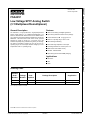
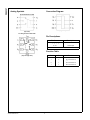
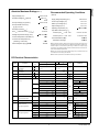
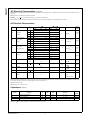
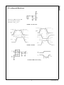
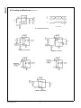
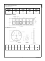
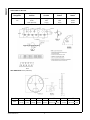
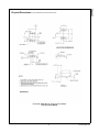
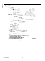
Revised August 2005
FSA3357
Low Voltage SP3T Analog Switch
(3:1 Multiplexer/Demultiplexer)
General Description
The FSA3357 is a high performance, single-pole/triple-throw
(SP3T) Analog Switch or 3:1 Multiplexer/Demultiplexer. The
device is fabricated with advanced sub-micron CMOS technology to achieve high speed enable and disable times and low On
Resistance. The break before make select circuitry prevents
disruption of signals on the B0, B1, or B2 Ports due to the
switches temporarily being enabled during select pin switching.
The device is specified to operate over the 1.65 to 5.5V VCC
operating range. The control input tolerates voltages up to 5.5V
independent of the VCC operating range.
Features
O Useful in both analog and digital applications
O Space saving US8 8-lead surface mount package
O Low On Resistance; 9: on typ @ 3.3V VCC
O Broad VCC operating range; 1.65V to 5.5V
O Rail-to-Rail signal handling
O Power down high impedance control input
O Overvoltage tolerance of control input to 7.0V
O Break before make enable circuitry
O 250 MHz - 3dB bandwidth
O Space saving Pb-Free MicroPak¥ packaging
Applications
O Cell Phone
O PDA
O Video
Ordering Code:
Product
Order
Package
Code
Number
Number
Top Mark
FSA3357K8X
MAB08A
A357
FSA3357L8X
MAC08A
FE
Package Description
Supplied As
8-Lead US8, JEDEC MO-187, Variation CA 3.1mm Wide 3k Units on Tape and Reel
Pb-Free 8-Lead MicroPak, 1.6 mm Wide
5k Units on Tape and Reel
Pb-Free package per JEDEC J-STD-020B.
MicroPak¥ is a trademark of Fairchild Semiconductor Corporation.
© 2005 Fairchild Semiconductor Corporation
DS500805
www.fairchildsemi.com
FSA3357 Low Voltage SP3T Analog Switch (3:1 Multiplexer/Demultiplexer)
December 2002
FSA3357
Analog Symbols
Connection Diagram
Pin Assignments for US8
(Top View)
(Top View)
Pin Assignments for MicroPak
Pin Descriptions
Pin Names
Description
A1, B0, B1, B2
Data Ports
S1, S2
Control Input
Function Table
(Top Through View)
www.fairchildsemi.com
2
S1
S2
Function
0
0
No Connection
1
0
B0 Connected to A
0
1
B1 Connected to A
1
1
B2 Connected to A
Recommended Operating Conditions
(Note 3)
0.5V to 7.0V
Supply Voltage (VCC)
0.5V to VCC
0.5V
DC Switch Voltage (VS) (Note 2)
Supply Voltage Operating (VCC)
0.5V to 7.0V
DC Input Voltage (VIN) (Note 2)
DC Input Diode Current (IIK)
@ (IIK) VIN 0V
50 mA
DC Output Current (IOUT)
r100 mA
150qC
Junction Temperature under Bias (TJ)
Junction Lead Temperature (TL)
260qC
(Soldering, 10 seconds)
Power Dissipation (PD) @ 85qC
0V to VCC
Output Voltage (VOUT)
0V to VCC
40qC to 85qC
Input Rise and Fall Time (tr, tf)
65qC to 150qC
Storage Temperature Range (TSTG)
0V to VCC
Switch Input Voltage (VIN)
Operating Temperature (TA)
128 mA
DC VCC or Ground Current (ICC/IGND)
1.65V to 5.5V
Control Input Voltage (VIN)
180 mW
Control Input VCC = 2.3V - 3.6V
0 ns/V to 10 ns/V
Control Input VCC = 4.5V - 5.5V
0 ns/V to 5 ns/V
Thermal Resistance (TJA)
250qC/W
MicroPak 8L Package
224qC/W
Note 1: Absolute maximum ratings are DC values beyond which the device may be
damaged or have its useful life impaired. The datasheet specifications should be met,
without exception, to ensure that the system design is reliable over its power supply,
temperature, and output/input loading variables. Fairchild does not recommend operation outside datasheet specifications.
Note 2: The input and output negative voltage ratings may be exceeded if the input
and output diode current ratings are observed.
Note 3: Control inputs must be held HIGH or LOW, they must not float.
DC Electrical Characteristics
Symbol
VIH
Parameter
HIGH Level
Input Voltage
VIL
LOW Level
Input Voltage
IIN
Input Leakage Current
IOFF
OFF State Leakage Current
RON
Switch On Resistance
TA = 25qC
VCC
(V)
Min
1.65 1.95
0.75 VCC
0.75 VCC
2.3 5.5
0.7 VCC
0.7 VCC
Max
Min
V
0.25 VCC
0.25 VCC
0.3 VCC
0.3 VCC
r0.1
r0.1
r1.0
r1.0
5.0
7.0
7.0
VIN = 0V, IO = 30 mA
6.0
12.0
12.0
VIN = 2.4V, IO = 30 mA
7.0
15.0
15.0
VIN = 4.5V, IO = 30 mA
6.5
9.0
9.0
VIN = 0V, IO = 24 mA
0 5.5
1.65 5.5
4.5
Rflat
PA
PA
:
0 d VIN d 5.5V
0 d A, Bn d VCC
VIN = 3V, IO = 24 mA
9.0
20.0
20.0
8.0
12.0
12.0
11.0
30.0
30.0
VIN = 2.3V, IO = 8 mA
1.65
10.0
20.0
20.0
VIN = 0V, IO = 4 mA
17.0
50.0
50.0
VIN = 1.65V, IO = 4 mA
1.0
10.0
PA
VCC
V
5.5
All Channels ON or OFF
'RON
V
2.3
Quiescent Supply Current
Analog Signal Range
Conditions
2.3 5.5
3.0
ASR
Units
Max
1.65 1.95
(Note 4)
ICC
Typ
TA = 40qC to 85qC
VCC
0.0
VCC
0.0
VIN = 0V, IO = 8 mA
VIN = VCC or GND
IOUT = 0
On Resistance Match
4.5
0.15
IA = 30 mA, VBn = 3.15
Between Channels
3.0
0.22
IA = 24 mA, VBn = 2.1
(Note 4)(Note 5)(Note 6)
2.3
0.31
1.65
0.62
IA = 4 mA, VBn = 1.15
IA = 30 mA, 0 d VBn d VCC
On Resistance Flatness
5.0
6.0
(Note 4)(Note 5)(Note 7)
3.3
12.0
2.5
40.0
1.8
140.0
:
:
IA = 8 mA, VBn = 1.6
IA = 24 mA, 0 d VBn d VCC
IA = 8 mA, 0 d VBn d VCC
IA = 4 mA, 0 d VBn d VCC
3
www.fairchildsemi.com
FSA3357
Absolute Maximum Ratings(Note 1)
FSA3357
DC Electrical Characteristics
(Continued)
Note 4: Measured by the voltage drop between A and Bn pins at the indicated current through the switch. On Resistance is determined by the lower of the voltages on the two (A
or Bn Ports).
Note 5: Parameter is characterized but not tested in production.
Note 6: 'RON = RON max RON min measured at identical VCC, temperature and voltage levels.
Note 7: Flatness is defined as the difference between the maximum and minimum value of On Resistance over the specified range of conditions.
AC Electrical Characteristics
Symbol
TA = 25qC
VCC
Parameter
(V)
Min
2.0
Bus to Bus
2.3 2.7
1.1
(Note 8)
3.0 3.6
0.7
Propagation Delay
tPLH
Min
32.0
5.0
34.0
2.3 2.7
3.0
15.0
3.0
16.5
(A to Bn)
3.0 3.6
2.0
9.5
2.0
11.0
4.5 5.5
1.5
6.5
1.5
7.0
3.0
14.0
3.0
14.5
Turn Off Time
2.3 2.7
2.0
7.2
2.0
7.8
(A Port to Bn Port)
3.0 3.6
1.5
5.1
1.5
5.5
3.7
0.8
4.0
tPHZ
Break Before Make Time
(Note 9)
Charge Injection (Note 9)
VI = OPEN
VI = 2 x VCC for tPZL
ns
1.65 1.95
Output Disable Time
Number
VI = 0V for tPZH
VI = 2 x VCC for tPLZ
ns
4.5 5.5
0.8
1.65 1.95
0.5
0.5
2.3 2.7
0.5
0.5
3.0 3.6
0.5
0.5
4.5 5.5
0.5
VI = 0V for tPHZ
ns
Off Isolation (Note 10)
Figures
1, 2
Figures
1, 2
Figure 3
0.5
5.0
3.0
3.3
2.0
1.65 5.5
58.0
CL = 0.1 nF, VGEN = 0V
pC
OIRR
Figures
1, 2
0.4
Turn on Time
tPLZ
Conditions
Max
5.0
tPZH
Figure
Units
ns
4.5 5.5
Output Enable Time
Q
Max
1.65 1.95
tPZL
tB-M
Typ
1.65 1.95
tPHL
TA = 40qC to 85qC
RGEN = 0:
RL = 50:
dB
Figure 4
Figure 5
f = 10MHz
Xtalk
1.65 5.5
Crosstalk
60.0
RL = 50:
dB
Figure 6
f = 10MHz
BW
3dB Bandwidth
THD
Total Harmonic Distortion
1.65 5.5
250.0
MHz
RL = 50:
Figure 9
RL = 600:
(Note 9)
5.0
.01
%
0.5 VP-P
f = 600 Hz to 20 KHz
Note 8: This parameter is guaranteed by design but not tested. The bus switch contributes no propagation delay other than the RC delay of the On Resistance of the switch and
the 50 pF load capacitance, when driven by an ideal voltage source (zero output impedance).
Note 9: Guaranteed by Design.
Note 10: Off Isolation = 20 log10 [VA / VBn]
Capacitance
(Note 11)
Figure
Symbol
Parameter
Typ
Max
Units
Conditions
Number
CIN
Control Pin Input Capacitance
2.0
pF
VCC = 0V
CIO-B
B Port Off Capacitance
3.6
pF
VCC = 5.0V
Figure 7
CIOA-ON
A Port Capacitance When Switch Is Enabled
14.5
pF
VCC = 5.0V
Figure 8
Note 11: TA = 25qC, f = 1 MHz, Capacitance is characterized but not tested in production.
www.fairchildsemi.com
4
FSA3357
AC Loading and Waveforms
Note: Input driven by 50: source terminated in 50:
Note: CL includes load and stray capacitance
Note: Input PRR = 1.0 MHz; tW = 500 ns
FIGURE 1. AC Test Circuit
FIGURE 2. AC Waveforms
FIGURE 3. Break Before Make Interval Timing
5
www.fairchildsemi.com
FSA3357
AC Loading and Waveforms
(Continued)
FIGURE 4. Charge Injection Test
FIGURE 5. Off Isolation
FIGURE 6. Crosstalk
FIGURE 7. Channel Off Capacitance
FIGURE 8. Channel On Capacitance
FIGURE 9. Bandwidth
www.fairchildsemi.com
6
FSA3357
Tape and Reel Specification
TAPE FORMAT for US8
Package
Tape
Number
Cavity
Cover Tape
Designator
Section
Cavities
Status
Status
Leader (Start End)
125 (typ)
Empty
Sealed
Carrier
250
Filled
Sealed
Trailer (Hub End)
75 (typ)
Empty
Sealed
K8X
TAPE DIMENSIONS inches (millimeters)
REEL DIMENSIONS inches (millimeters)
Tape
Size
A
B
C
D
N
W1
W2
W3
7.0
0.059
0.512
0.795
2.165
0.331 0.059/
0.000
0.567
W1 0.078/0.039
(177.8)
(1.50)
(13.00)
(20.20)
(55.00)
(8.40 1.50/0.00)
(14.40)
(W1 2.00/1.00)
8 mm
7
www.fairchildsemi.com
FSA3357
TAPE FORMAT for MicroPak
Package
Tape
Number
Cavity
Cover Tape
Designator
Section
Cavities
Status
Status
Leader (Start End)
125 (typ)
Empty
Sealed
L8X
Carrier
5000
Filled
Sealed
Trailer (Hub End)
75 (typ)
Empty
Sealed
REEL DIMENSIONS inches (millimeters)
Tape Size
8 mm
www.fairchildsemi.com
A
B
C
D
N
W1
W2
W3
7.0
0.059
0.512
0.795
2.165
0.331 0.059/0.000
0.567
W1 0.078/0.039
(177.8)
(1.50)
(13.00)
(20.20)
(55.00)
(8.40 1.50/0.00)
(14.40)
(W1 2.00/1.00)
8
FSA3357
Physical Dimensions inches (millimeters) unless otherwise noted
8-Lead US8, JEDEC MO-187, Variation CA 3.1mm Wide
Package Number MAB08A
9
www.fairchildsemi.com
FSA3357
Physical Dimensions inches (millimeters) unless otherwise noted (Continued)
Pb-Free 8-Lead MicroPak, 1.6 mm Wide
Package Number MAC08A
www.fairchildsemi.com
10
FAIRCHILD SEMICONDUCTOR RESERVES THE RIGHT TO MAKE CHANGES WITHOUT FURTHER NOTICE TO ANY
PRODUCTS HEREIN TO IMPROVE RELIABILITY, FUNCTION OR DESIGN. FAIRCHILD DOES NOT ASSUME ANY LIABILITY
ARISING OUT OF THE APPLICATION OR USE OF ANY PRODUCT OR CIRCUIT DESCRIBED HEREIN; NEITHER DOES IT
CONVEY ANY LICENSE UNDER ITS PATENT RIGHTS, NOR THE RIGHTS OF OTHERS.
LIFE SUPPORT POLICY
FAIRCHILD’S PRODUCTS ARE NOT AUTHORIZED FOR USE AS CRITICAL COMPONENTS IN LIFE SUPPORT DEVICES
OR SYSTEMS WITHOUT THE EXPRESS WRITTEN APPROVAL OF FAIRCHILD SEMICONDUCTOR CORPORATION
As used herein:
provided in the labeling, can be reasonably expected to
result in significant injury to the user.
1. Life support devices or systems are devices or systems
which, (a) are intended for surgical implant into the body, or
2. A critical component is any component of a life support
(b) support or sustain life, or (c) whose failure to perform
device or system whose failure to perform can be reasonwhen properly used in accordance with instructions for use
ably expected to cause the failure of the life support device
or system, or to affect its safety or effectiveness.
PRODUCT STATUS DEFINITIONS
Definition of terms
Datasheet Identification Product Status
Definition
Advance Information
Formative or In Design
This datasheet contains the design specifications for product development. Specifications may change in any manner without notice.
Preliminary
First Production
This datasheet contains preliminary data, and supplementary data will
be published at a later date. Fairchild Semiconductor reserves the right
to make changes at any time without notice in order to improve design.
No Identification Needed
Full Production
This datasheet contains final specifications. Fairchild Semiconductor
reserves the right to make changes at any time without notice in order
to improve design.
Obsolete
Not In Production
This datasheet contains specifications on a product that has been discontinued by Fairchild Semiconductor. The datasheet is printed for reference information only.
11
www.fairchildsemi.com
FSA3357 Low Voltage SP3T Analog Switch (3:1 Multiplexer/Demultiplexer)
DISCLAIMER


![Technologie des circuit intégrés (composants) [Format PDF]](http://vs1.manualzilla.com/store/data/006460848_1-f135636d429cc786ac12f54c88c1d7c9-150x150.png)