1
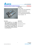
OPEP-33-A4Q1RI
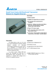
1.25Gbps Upstream/1.25Gbps Downstream
Intelligent GE-PON ONU Transceiver
FEATURES
z RoHS compliant
z Digital Diagnostic SFF-8472 MSA compliant
z Support extended operating Case
temperature from -20ºC to +85ºC
z IEEE802.3ah Gigabit Ethernet compliant
z SFF package with SC Receptacle
z 1310nm Burst Mode 1.25Gbps transmitter,
and 1490nm Continuous Mode 1.25Gbps
receiver
z Integrated with WDM filter to cut 1550nm and
1650nm optical signal off
z Single +3.3V power supply with LVPECL
electrical signal interface, LVTTL Bias
Control input and Rx Signal Detect output
z Laser Class 1 Product which comply with the
requirements of IEC 60825-1 and IEC 60825-2
Description
DELTA’s
Application
GE-PON
ONU
z IEEE 802.3ah 1000BASE-PX10-U
transceiver
OPEP-33-A4Q1RI is designed for Gigabit Ethernet
Passive Optical Network transmission.
z GE-PON ONU
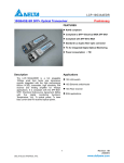
The module is contained in a SFF package
with standard SC receptacle connector.
z FTTx WDM Broadband Access
z Burst Mode Application
The module consists 1310nm FP laser,
InGaAs PIN, Preamplifier and WDM filter in a
high-integrated optical sub-assembly, and it
receives up to 1.25Gbps of continuous data at
1490nm, and transmits 1.25Gbps of burst-mode
z OPEP-33-A4Q1RI data link up to 10km in
9/125um single mode fiber.
data at 1310nm.
1
DELTA ELECTRONICS, INC.
Revision: S3
12/20/2007
www.deltaww.com
OPEP-33-A4Q1RI
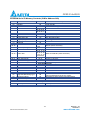
1. Absolute Maximum Ratings
Parameter
Storage Temperature
Storage Ambient Humidity
Power Supply Voltage
Signal Input Voltage
Receiver Damage Threshold
Lead Soldering Temperature
Lead Soldering Time
Symbol
Ts
HA
VCC
Min.
-40
5
-0.3
-0.3
+2
Typ.
TSOLD
tSOLD
Max.
85
95
4
Vcc+0.3
260
10
Unit
ºC
%
V
V
dBm
ºC
sec
Note
Unit
ºC
%
V
mA
mVp-p
Note
Note (1)
2. Recommended Operating Conditions
Parameter
Operating Case Temperature
Ambient Humidity
Power Supply Voltage
Power Supply Current
Power Supply Noise Rejection
Symbol
TC
HA
VCC
ICC
Min.
-20
5
3.13
1.25
Data Rate
-100ppm
Typ.
3.3
1.25
Transmission Distance
Max.
+85
85
3.47
300
100
1.25
+100ppm
Non-condensing
100Hz to 1MHz
Gbps
10
km
Typ.
Max.
+4
+4.5
+7.5
1310
1360
Unit
dBm
dBm
dBm
dB
nm
nm
dBm
Note (1). Measured on topside of case front center
.
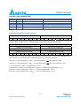
3. Specification of Transmitter
Parameter
Average Launched Power (B.O.L)
Average Launched Power (E.O.L)
Launched power (Peak.)
Extinction Ratio
Center Wavelength
Spectrum Width (RMS)
Transmitter OFF Output Power
Laser Burst On Time
Laser Burst Off Time
Optical Rise/Fall Time
Total Jitter
Optical Return Loss Tolerance
Relative Intensity Noise
Optical Transmitter Reflectance
Transmitter and Dispersion Penalty
Output Eye Mask
{X1,X2,Y1,Y2,Y3}
Symbol
PO
PO
PP
ER
λC
σ
POff
Ton
Toff
tr/tf
tJ
ORLT
RIN15OMA
Min.
-0.5
-1
9
1260
Compliant with IEEE 802.3ah
-45
32
32
260
128
15
-113
-6
TDP
2.8
Compliant with IEEE 802.3ah
{0.22,0.375,0.20,0.20,0.30}
ps
ps
dB
dB/Hz
dB
dB
Note
Note (1)
Note (1)
FP Laser
Note (4)
Note (2)
Note (3)
Note (5)
Note (1). Launched power (avg.) is power coupled into a single mode fiber with master connector.
B.O.L=Before of Life; E.O.L= End of Life
Note (2). These are unfiltered 20-80% values.
Note (3). Measure at 27-1 NRZ PRBS pattern
2
DELTA ELECTRONICS, INC.
Revision: S3
12/20/2007
www.deltaww.com
OPEP-33-A4Q1RI
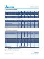
Note (4). Transmitter spectral limits
Center Wavelength
Transmitter Spectral Limits
4
3
RMS (nm)
nm
1260
1270
1280
1290
1295
1297
1329
1331
1340
1350
1360
RMS spectral width(max)
1000Base-PX10-U
nm
2.09
2.52
3.13
2
3.50
1
0
3.06
2.58
1240
1260
1280
1300
1320
Center Wavelength (nm)
1340
1360
1380
Note (5). Transmitter eye mask definition
1+ Y 3
Normalized Amplitude
1
1- Y1
0.5
Y1
0
- Y2
0
X1
X2
1- X2 1- X1
1
Normalized Time
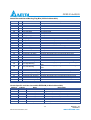
4. Specification of Receiver
Parameter
Input Optical Wavelength
Receiver Sensitivity
Input Saturation Power (Overload)
Signal Detect -Assert Power
Signal Detect -Deassert Power
Signal Detect Hysteresis
Data Output Rise/Fall time
Receiver
1480 to 1500nm
Reflectance
Optical Isolation 1260 to 1360nm
from
External 1550 to 1560nm
Source
1640 to 1665nm
Symbol
λIN
PIN
PSAT
PA
PD
PA-PD
tr/tf
Min.
1480
-3
-44
0.5
3
DELTA ELECTRONICS, INC.
Typ.
1490
Max.
1500
-26
6
260
Unit
nm
dBm
dBm
dBm
dBm
dB
ps
-12
dB
-43
-33
-33
dB
dB
dB
-26
2
Note
PIN-PD
Note (1)
Note (2)
Note (3)
Note (4)
Revision: S3
12/20/2007
www.deltaww.com
OPEP-33-A4Q1RI
Note (1). Measured with Light source +1dBm, 1490nm, ER=9dB; BER =<10-12@PRBS=27-1 NRZ
This assurance should be met with asynchronous data flowing out of the optical transmitter of
the system under test. The output data pattern from the transmitter of the system under test is a
repetition of alternate 0/1 pattern as defined for this measurement.
Note (2). When SD deasserted, the data output is Low-level (fixed)
Note (3). These are 20%~80% values.
Note (4). Measured at wavelength of 1490nm.
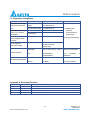
5. Electrical Interface Characteristics
Parameter
Transmitter
Total Supply Current
Differential line input Impedance
Differential Data Input Swing
Data Input Voltage- High
Data Input Voltage- Low
BiasCNT Input Voltage- High
BiasCNT Input Voltage- Low
Receiver
Total Supply Current
Differential Data Output Swing
Signal Detect Output Voltage-High
Signal Detect Output Voltage-Low
Symbol
Min.
Typ.
ICC
RIN
VDT
VIH-VCC
VIL-VCC
VBCH
VBCL
80
200
-1.165
-1.810
2
0
100
ICC
VDR
VLOSH
VLOSL
400
2
0
Max.
Unit
Note
A
120
1600
-0.880
-1.475
Vcc
0.8
mA
Ohm
mVp-p
V
V
V
V
Note (1)
B
1600
Vcc+0.3
0.8
mA
mVp-p
V
V
LVPECL
LVTTL
Note (1)
Note (2)
LVTTL
Note (1). A (TX)+ B (RX) = 300mA (Not include termination circuit)
Note (2). Internally AC coupled, but requires a 100Ohm differential termination at or internal to Serializer/
Deserializer.
4
DELTA ELECTRONICS, INC.
Revision: S3
12/20/2007
www.deltaww.com
OPEP-33-A4Q1RI
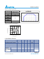
6. Transmitter Burst Mode Timing Characteristics
Parameter
BiasCNT Enable Duration
Interval of BiasCNT Signal
Symbol
Min.
1
0.112
Typ.
Max.
1000000
Unit
us
us
Note
BiasCNT Enable Duration
BiasCNT
Interval of BiasCNT Signal
VccT
VccT < 3.1V
BiasCNT
X
Low
High
VccT > 3.1V
Data Input
X
X
Floating
Present
Optical Output
OFF
OFF
Other
Laser bias and modulation signal output
X = Don’t care
Other = Less than +7.5dBm (peak)
High = Logic high level, Low = logic low level
Floating = No Data Input, Present = Data Input,
OFF = Optical Power is less than –45dBm
H
BiasCNT
L
Data Input
Optical Output
Within 15% of steady state
Ton
Toff
7. Digital Diagnostic Monitor Accuracy
Parameter
Transceiver Internal Temperature
Power Supply Internal Voltage
TX Bias Current
TX Optical Power
RX Optical Power
Accuracy
Unit
± 3℃
℃
± 3%
± 10%
± 3dB
± 3dB
V
mA
dBm
dBm
Calibration
Internal
Internal
Internal
Internal
Internal
Note
TC=-20~+85℃
VCC=3.3V±5%
Specified by nominal bias value
Not support in burst ONU
-26 to -3dBm
Note. Temperature and Voltage is measured internal to the transceiver.
5
DELTA ELECTRONICS, INC.
Revision: S3
12/20/2007
www.deltaww.com
OPEP-33-A4Q1RI
8. Pin Description
Tx/Rx
Pin No.
1
2
I/O
Rx
3
O
4
5
6
7
8
9
10
11
12
13
14
O
O
Tx
I
I
I
I/O
I
Pin Name
Description
VeeR
Receiver Ground
VccR
+3.3V Receiver Power Supply
SD
Normal Optical Input indicated by logic “High”, and No Optical
Input indicated by logic “Low”.
RD(n)
Inverted Receiver Data Output (AC-Coupled)
RD(p)
Non-Inverted Receiver Data Output (AC-Coupled)
VccT
+3.3V Transmitter Power Supply
VeeT
Transmitter Ground
BiasCNT Positive pulse which control the ONU burst mode operation
TD(p)
Non-Inverted Transmitter Data Input
TD(n)
Inverted Transmitter Data Input
VeeT
Transmitter Ground
NC
Not Connect
SDA
I2C Serial Data Input/Output (LVTTL) (Mod-Def 2)
SCL
I2C Serial Clock Input (LVTTL) (Mod-Def 1)
MS
Mounting Studs/Connect this pin to Chassis ground
HL
EMI Shielding Leads/ connect this pin to Chassis/ Signal ground
6
DELTA ELECTRONICS, INC.
Revision: S3
12/20/2007
www.deltaww.com
OPEP-33-A4Q1RI
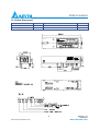
9. Recommended Interface Circuit
DELTA GEPON ONU Module
1uH
6. VccT
3.3V
10uF
100nF
100nF
1uH
8.BiasCNT
BiasCNT
9. TD(p)
Coupled
interface
Transmitter
10. TD(n)
7. VeeT
SerDes IC
1. VeeR
10uF
Protocol IC
100nF
5. RD(p)
Z0=50ohm
100nF
100ohm
4.RD(n)
Z0=50ohm
100nF VccR
3. SD
SD
Receiver
RES
3.3V
2. VccR
RES
RES
11. SDA
SDA
EEPROM
12. SCL
SCL
* RES is the internal 4.7K to 10K Ohms pull-up resistor.
DC - Coupled interface
Coupled
interface
AC - Coupled interface
3.3V
130ohm
Z0=50ohm
Host
Board
82ohm
100nF
100ohm
DELTA
ONU
Z0=50ohm
Host
Board
Z0=50ohm
150ohm
DELTA
ONU
Z0=50ohm
130ohm
150ohm
100nF
82ohm
3.3V
7
DELTA ELECTRONICS, INC.
Revision: S3
12/20/2007
www.deltaww.com
OPEP-33-A4Q1RI
10. Outline Dimensions
Parameter
Mechanical Dimensions
Connector Type
Unit
mm
-
Description
48.3x13.5x9.6
SC/UPC connector
Note
IEC-61754-4
.
J
r
e
t
p
a
h
c
b
u
S
R
F
n
oC
i
t
1
a
2
i
t
,
c ds
a
u
d
d ra
r
A
o
d
r
Dn
P
Ft
a
rh
s
e
te
s
i
aw
c
n
Ls
a
em
1l
i
r
s po
s
mr
f
a
l
oe
C
Cp
W eek (52W eeks/Y ear) : 1月 2日 =01
8
DELTA ELECTRONICS, INC.
Revision: S3
12/20/2007
www.deltaww.com
OPEP-33-A4Q1RI
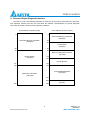
11. Enhanced Digital Diagnostic Interface
The memory map in the following describes an extension to the memory map defined in SFF-8472.
The enhanced interface uses the two wire serial bus address 1010001X(A2h) to provide diagnostic
information about the module’s present operating conditions.
2 wire address 1010000 X (A0h)
2 wire address 1010001 X (A2h)
0
0
Alarm and Warning Thresholds
(56 bytes)
Serial ID Defined by SFP MSA
(96 bytes)
55
56
Cal Constants
(40 bytes)
95
96
95
96
Real Time Diagnostic Interface
(24 bytes)
Vender Specific
(32 bytes)
119
120
Vender Specific
127
127
128
128
User Writable EEPROM
(120 bytes)
Reserved in SFP MSA
(128 bytes)
247
248
255
255
9
DELTA ELECTRONICS, INC.
Vender Specific
(8 bytes)
Revision: S3
12/20/2007
www.deltaww.com
OPEP-33-A4Q1RI
EEPROM Serial ID Memory Contents (2-Wire Address A0h)
Address
Name of Field
Hex
Description
Base ID Fields
00
Identifier
80
Vendor specific
01
Ext. Identifier
04
Serial ID module supported
02
Connector
01
SC connector
00 00 00 80
03-10 Transceiver Codes
BASE-PX
00 00 00 00
11
Encoding
01
Compatible with 8B/10B encoding code
12
BR, Nominal
0D
Nominal 1250Mbps
13
Reserved
00
14
Length (9um)-km
0A
10km @9/125um fiber
15
Length (9um)-100m
64
10000m @9/125um fiber
16-18 Length for MMF
00
Undefined in MMF
19
Reserved
00
Vendor Name
44 45 4C 54
20-35
“DELTA” (ASCII character)
41 20
36
Channel Spacing
00
Undefined
37-39 Vendor OUI
00
Undefined
4F 50 45 50
2D 33 33 2D
40-55 Vendor P/N
“OPEP-33-A4Q1RI” (ASCII character)
41 34 51 31
52 49 20 20
56-59 Vendor P/N Rev.
41 20 20 20 “A” (ASCII character)
60-61 Laser Wavelength
05 1E
1310nm in Hex byte
62
DWDM Wavelength Fraction
00
Undefined
63
CC_BASE
XX
Check sum of bytes 0-62
Extended ID Fields
64-65 Options
00 00
66
BR, Max.
00
67
BR, Min.
00
68-83 Vendor SN
XX
“DEYYWWVVRSSSSS” in ASCII character
84-91 Date Code
XX
“YYMMDD” in ASCII character
Implemented with internal calibration and received
92
Diagnostic Monitoring Type
68
power measurement type by Avg. power
93
Enhanced options
80
Alarm/Warning flags monitor are implemented
94
SFF-8472 compliant
01
SFF-8472 compliant with revision 9.3
95
CC_EXT
XX
Check sum of bytes 64-94
Vendor Specific ID Fields
96-127 Vendor Specific
00
Vendor specific EEPROM
128-256 Reserved
00
Reserved for future use
10
DELTA ELECTRONICS, INC.
Revision: S3
12/20/2007
www.deltaww.com
OPEP-33-A4Q1RI
Digital Diagnostic Monitoring Interface (2-Wire Address A2h)
Alarm and Warning Thresholds (2 Wire Address A2h)
Address
00-01
02-03
04-05
06-07
08-09
10-11
12-13
14-15
16-17
18-19
20-21
22-23
24-25
26-27
28-29
30-31
32-33
34-35
36-37
38-39
40-55
# Bytes
2
2
2
2
2
2
2
2
2
2
2
2
2
2
2
2
2
2
2
2
16
Name of Field
Temp High Alarm
Temp Low Alarm
Temp High Warning
Temp Low Warning
Voltage High Alarm
Voltage Low Alarm
Voltage High Warning
Voltage Low Warning
Bias High Alarm
Bias Low Alarm
Bias High Warning
Bias Low Warning
TX Power High Alarm
TX Power Low Alarm
TX Power High Warning
TX Power Low Warning
RX Power High Alarm
RX Power Low Alarm
RX Power High Warning
RX Power Low Warning
Reserved
HEX
64 00
DD 00
5A 00
E7 00
94 70
6D 60
87 8C
7A 44
4E 20
01 F4
3A 98
01 F4
Real Value
100℃
-35℃
90℃
-25℃
3.8
2.8
3.47
3.13
40
1
30
1
Unit
ºC
ºC
ºC
ºC
V
V
V
V
mA
mA
mA
mA
No implemented for Burst Mode.
27 10
00 0D
13 94
00 19
0
-29
-3
-26
dBm
dBm
dBm
dBm
Calibration Constants (2 Wire Address A2h)
Address
56-59
60-63
64-67
68-71
72-75
76-77
78-79
80-81
82-83
84-85
86-87
88-89
90-91
92-94
95
# Bytes
4
4
4
4
4
2
2
2
2
2
2
2
2
3
1
Name of Field
Rx_PWR (4)
Rx_PWR (3)
Rx_PWR (2)
Rx_PWR (1)
Rx_PWR (0)
Tx_I (Slope)
Tx_I (Offset)
Tx_PWR (Slope)
Tx_PWR (Offset)
T (Slope)
T (Offset)
V (Slope)
V (Offset)
Reserved
Checksum
HEX
00 00 00 00
00 00 00 00
00 00 00 00
3F 80 00 00
00 00 00 00
01 00
00 00
01 00
00 00
01 00
00 00
01 00
00 00
00 00 00
XX
11
DELTA ELECTRONICS, INC.
Description
Set to zero for “internally calibrated” devices.
Set to zero for “internally calibrated” devices.
Set to zero for “internally calibrated” devices.
Set to 1 for “internally calibrated” devices.
Set to zero for “internally calibrated” devices.
Set to 1 for “internally calibrated” devices.
Set to zero for “internally calibrated” devices.
Set to 1 for “internally calibrated” devices.
Set to zero for “internally calibrated” devices.
Set to 1 for “internally calibrated” devices.
Set to zero for “internally calibrated” devices.
Set to 1 for “internally calibrated” devices.
Set to zero for “internally calibrated” devices.
Reserved
Checksum of bytes 0 – 94.
Revision: S3
12/20/2007
www.deltaww.com
OPEP-33-A4Q1RI
A/D Value (2 Wire Address A2h)
Address
96-97
98-99
100-101
102-103
104-105
106-109
# Bytes
2
2
2
2
2
4
Name of Field
Temperature (MSB, LSB)
Supply Voltage (MSB, LSB)
Tx Bias Current (MSB, LSB)
Tx Optical Power (MSB, LSB)
Rx Received Power (MSB, LSB)
Reserved
Description
Internally measured module temperature
Internally measured supply voltage in module
Internally measured Tx Bias current
No implemented for Burst Mode.
Measured Rx input power
Notes:
Temperature (Signed twos complement value)
A2h Byte 96 (Temperature MSB)
S
6
2
5
2
4
2
3
2
2
2
A2h Byte 97 (Temperature LSB)
1
2
0
-1
2
2
-2
2
-3
2
-4
2
-5
2
-6
2
-7
2
1
2
2
-8
Supply Voltage, Tx Bias Current, Tx Optical Power, Rx Received Power (Unsigned values)
A2h Byte 98 (Vcc MSB)
A2h Byte 99 (Vcc LSB)
A2h Byte 100 (TX Bias MSB)
A2h Byte 101 (TX Bias LSB)
A2h Byte 102 (TX Power MSB)
A2h Byte 103 (TX Power LSB)
A2h Byte 104 (RX Power MSB)
15
2
14
2
13
2
12
2
11
2
10
2
A2h Byte 105 (RX Power LSB)
9
2
8
7
2
2
6
2
5
2
4
2
3
2
2
2
2
0
The digital value conversions are updated every 13ms (nominal) or 20ms (max) in rotation. After getting digital value,
each measurement could be obtained by multiplying digital value by corresponding LSB value:
1
Temperature = Temp (Digital Value) × LSBTemp = Temp (Digital Value) × 256; when Temperature<128
1
Temperature = Temp (Digital Value) × LSBTemp = [Temp (Digital Value) × 256]-256; when Temperature≧128
Vcc = Vcc(Digital Value) × LSBVcc=VCC(Digital Value) × 100µV
TX Bias Current = TX Bias Current (Digital Value) × LSBTX,Bias = TX Bias Current (Digital Value) × 2µA
TX Power = TX Power (Digital Value) × LSBTXPower = TX Power (Digital Value) × 0.1µW
RX Power = RX Power (Digital Value) × LSBRXPower = RX Power (Digital Value) × 0.1µW
12
DELTA ELECTRONICS, INC.
Revision: S3
12/20/2007
www.deltaww.com
OPEP-33-A4Q1RI
Status Bits and Alarm/Warning Flag Bits (2 Wire Address A2h)
Address
110
110
110
110
110
110
110
110
111
112
112
112
112
112
112
112
112
113
113
113
114-115
116
116
Bit
7
6
5
4
3
2
1
0
All
7
6
5
4
3
2
1
0
7
6
5-0
All
7
6
Name
TX Disable State
Soft TX Disable
Reserved
RX Rate Select State
Soft RX Rate Select
TX Fault State
Signal Detect State
Data_Ready_Bar
Reserved
Temp High Alarm
Temp Low Alarm
Vcc High Alarm
Vcc Low Alarm
TX Bias High Alarm
TX Bias Low Alarm
TX Power High Alarm
TX Power Low Alarm
RX Power High Alarm
RX Power Low Alarm
Reserved Alarm
Reserved
Temp High Warning
Temp Low Warning
116
5
Vcc High Warning
116
4
Vcc Low Warning
116
116
116
116
117
117
117
118-119
3
2
1
0
7
6
5-0
All
TX Bias High Warning
TX Bias Low Warning
TX Power High Warning
TX Power Low Warning
RX Power High Warning
RX Power Low Warning
Reserved Warning
Reserved
Description
No implemented.
No implemented.
No implemented.
No implemented.
No implemented.
No implemented.
No implemented.
Set when internal temperature exceeds high alarm level.
Set when internal temperature is below low alarm level.
Set when internal supply voltage exceeds high alarm level.
Set when internal supply voltage is below low alarm level.
Set when TX Bias current exceeds high alarm level.
Set when TX Bias current is below low alarm level.
No implemented for Burst Mode.
No implemented for Burst Mode.
Set when Received Power exceeds high alarm level.
Set when Received Power is below low alarm level.
Set when internal temperature exceeds high warning level.
Set when internal temperature is below low warning level.
Set when internal supply voltage exceeds high warning
level.
Set when internal supply voltage is below low warning
level.
Set when TX Bias current exceeds high warning level.
Set when TX Bias current is below low warning level.
No implemented for Burst Mode.
No implemented for Burst Mode.
Set when Received Power exceeds high warning level.
Set when Received Power is below low warning level.
Vendor Specific and User Accessible EEPROM (2 Wire Address A2h)
Address
120-122
123
124
125
126
127
128-247
248-255
# Bytes
3
1
1
1
1
1
120
8
Name
Reserved
Password Byte 3
Password Byte 2
Password Byte 1
Password Byte 0
User EEPROM Select
User EEPROM
Vendor Specific
Description
High order byte of 32 bit password
Second highest order byte of 32 bit password
Second lowest order byte of 32 bit password
Low order byte of 32 bit password
“1” selects user writable EEPROM at locations 128-247
User writable EEPROM
Vendor specific control functions
13
DELTA ELECTRONICS, INC.
Revision: S3
12/20/2007
www.deltaww.com
OPEP-33-A4Q1RI
12. Regulatory Compliance
Feature
Test Method
Electrostatic Discharge
(ESD) to the Electrical
Pins
Human Body Model MIL-STD-883E Method 3015.7
(HBM)
EIA-JESD22-A114
Electrostatic Discharge
(ESD) to the Simplex
Receptacle
Contact Discharge
Machine Model (MM) EIA-JESD22-A115
Air Discharge
Radio Frequency
Electromagnetic Field
Immunity
IEC/EN 61000-4-2
IEC/EN 61000-4-2
IEC/EN 61000-4-3
Performance
(1) Satisfied with
electrical
characteristics of
product spec.
(2) No physical damage
FCC Part 15 Class B
EN 55022 Class B
(CISPR 22A)
Electromagnetic
Interference (EMI)
Laser Eye Safety
Reference
FDA/CDRH
FDA 21CFR 1040.10, 1040.11
CDRH File # 0420993
TUV
IEC/EN 60825-1
IEC/EN 60825-2
TUV
Certificate
R50032471
TUV
IEC/EN 60950
UL/CSA
UL 60950
#
Component Recognition
UL File # E239394
Appendix A. Document Revision
Version No.
S0
S1
S2
S3
Date
2006-11-06
2007-08-08
2007-10-10
2007-12-20
Description
Preliminary Datasheet
Change the PIN outline, DDM accuracy and Differential Data Input Swing
Update the DDM description and Receiver Saturation
Update the DDM contents
14
DELTA ELECTRONICS, INC.
Revision: S3
12/20/2007
www.deltaww.com