1
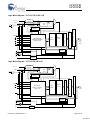
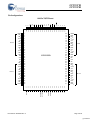
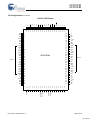
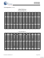
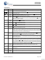
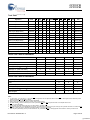
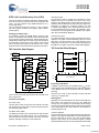
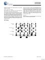
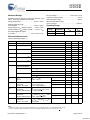
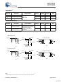
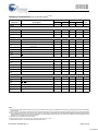
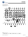
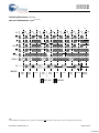
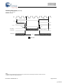
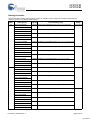
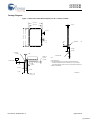
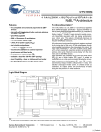
CY7C1371D
CY7C1373D
18-Mbit (512K x 36/1M x 18)
Flow-Through SRAM with NoBL™ Architecture
Functional Description[1]
Features
• No Bus Latency™ (NoBL™) architecture eliminates dead
cycles between write and read cycles
• Supports up to 133-MHz bus operations with zero wait
states
— Data is transferred on every clock
• Pin-compatible and functionally equivalent to ZBT™
devices
• Internally self-timed output buffer control to eliminate the
need to use OE
• Registered inputs for flow through operation
• Byte Write capability
• 3.3V/2.5V IO power supply (VDDQ)
• Fast clock-to-output times
— 6.5 ns (for 133-MHz device)
• Clock Enable (CEN) pin to enable clock and suspend
operation
• Synchronous self-timed writes
• Asynchronous Output Enable
• Available in JEDEC-standard Pb-free 100-pin TQFP,
Pb-free and non-Pb-free 119-Ball BGA and 165-Ball FBGA
package.
The CY7C1371D/CY7C1373D is a 3.3V, 512K x 36/1M x 18
Synchronous flow through Burst SRAM designed specifically
to support unlimited true back-to-back Read/Write operations
with no wait state insertion. The CY7C1371D/CY7C1373D is
equipped with the advanced No Bus Latency (NoBL) logic
required to enable consecutive Read/Write operations with
data being transferred on every clock cycle. This feature
dramatically improves the throughput of data through the
SRAM, especially in systems that require frequent Write-Read
transitions.
All synchronous inputs pass through input registers controlled
by the rising edge of the clock. The clock input is qualified by
the Clock Enable (CEN) signal, which when deasserted
suspends operation and extends the previous clock cycle.
Maximum access delay from the clock rise is 6.5 ns (133-MHz
device).
Write operations are controlled by the two or four Byte Write
Select (BWX) and a Write Enable (WE) input. All writes are
conducted with on-chip synchronous self-timed write circuitry.
Three synchronous Chip Enables (CE1, CE2, CE3) and an
asynchronous Output Enable (OE) provide for easy bank
selection and output tri-state control. To avoid bus contention,
the output drivers are synchronously tri-stated during the data
portion of a write sequence.
• Three chip enables for simple depth expansion
• Automatic Power down feature available using ZZ mode or
CE deselect
• IEEE 1149.1 JTAG-Compatible Boundary Scan
• Burst Capability — linear or interleaved burst order
• Low standby power
Selection Guide
133 MHz
100 MHz
Unit
Maximum Access Time
6.5
8.5
ns
Maximum Operating Current
210
175
mA
Maximum CMOS Standby Current
70
70
mA
Note:
1. For best-practices recommendations, please refer to the Cypress application note System Design Guidelines on www.cypress.com.
Cypress Semiconductor Corporation
Document #: 38-05556 Rev. *F
•
198 Champion Court
•
San Jose, CA 95134-1709
•
408-943-2600
Revised July 09, 2007
[+] Feedback
CY7C1371D
CY7C1373D
Logic Block Diagram – CY7C1371D (512K x 36)
ADDRESS
REGISTER
A0, A1, A
A1
D1
A0
D0
MODE
CLK
CEN
C
CE
ADV/LD
C
BURST
LOGIC
Q1 A1'
A0'
Q0
WRITE ADDRESS
REGISTER
ADV/LD
BW A
WRITE
DRIVERS
WRITE REGISTRY
AND DATA COHERENCY
CONTROL LOGIC
BW B
BW C
MEMORY
ARRAY
S
E
N
S
E
A
M
P
S
BW D
WE
INPUT
REGISTER
OE
CE1
CE2
CE3
D
A
T
A
S
T
E
E
R
I
N
G
O
U
T
P
U
T
B
U
F
F
E
R
S
DQs
DQP A
DQP B
DQP C
DQP D
E
E
READ LOGIC
SLEEP
CONTROL
ZZ
Logic Block Diagram – CY7C1373D (1M x 18)
ADDRESS
REGISTER
A0, A1, A
A1
D1
A0
D0
MODE
CLK
CEN
C
CE
ADV/LD
C
BURST
LOGIC
Q1 A1'
A0'
Q0
WRITE ADDRESS
REGISTER
ADV/LD
BW A
BW B
WRITE REGISTRY
AND DATA COHERENCY
CONTROL LOGIC
WRITE
DRIVERS
MEMORY
ARRAY
S
E
N
S
E
A
M
P
S
WE
OE
CE1
CE2
CE3
ZZ
Document #: 38-05556 Rev. *F
INPUT
REGISTER
D
A
T
A
S
T
E
E
R
I
N
G
O
U
T
P
U
T
B
U
F
F
E
R
S
DQs
DQP A
DQP B
E
E
READ LOGIC
SLEEP
CONTROL
Page 2 of 29
[+] Feedback
CY7C1371D
CY7C1373D
Pin Configurations
A
42
43
44
45
46
47
48
49
50
NC/36M
A
A
A
A
A
A
A
41
NC/72M
40
37
A0
VSS
36
A1
VDD
35
A
39
34
A
NC/144M
33
A
38
32
NC/288M
31
Document #: 38-05556 Rev. *F
81
A
82
A
83
A
84
ADV/LD
85
OE
86
90
CEN
VSS
91
WE
VDD
92
88
CE3
93
CLK
BWA
94
89
BWC
96
BWB
BWD
97
95
CE2
98
A
CE1
87
80
79
78
77
76
75
74
73
72
71
70
69
68
67
66
65
64
63
62
61
60
59
58
57
56
55
54
53
52
51
CY7C1371D
A
BYTE D
1
2
3
4
5
6
7
8
9
10
11
12
13
14
15
16
17
18
19
20
21
22
23
24
25
26
27
28
29
30
MODE
BYTE C
DQPC
DQC
DQC
VDDQ
VSS
DQC
DQC
DQC
DQC
VSS
VDDQ
DQC
DQC
NC
VDD
NC
VSS
DQD
DQD
VDDQ
VSS
DQD
DQD
DQD
DQD
VSS
VDDQ
DQD
DQD
DQPD
99
100
A
100-Pin TQFP Pinout
DQPB
DQB
DQB
VDDQ
VSS
DQB
DQB
DQB
DQB
VSS
VDDQ
DQB
DQB
VSS
NC
VDD
ZZ
DQA
DQA
VDDQ
VSS
DQA
DQA
DQA
DQA
VSS
VDDQ
DQA
DQA
DQPA
BYTE B
BYTE A
Page 3 of 29
[+] Feedback
CY7C1371D
CY7C1373D
Pin Configurations (continued)
A
42
43
44
45
46
47
48
49
50
NC/36M
A
A
A
A
A
A
A
41
NC/72M
40
37
A0
VSS
36
A1
VDD
35
A
39
34
A
NC/144M
33
A
38
32
NC/288M
31
Document #: 38-05556 Rev. *F
81
A
82
A
83
A
84
ADV/LD
85
OE
86
90
CEN
VSS
91
87
VDD
92
WE
CE3
93
CLK
BWA
94
89
NC
BWB
95
NC
97
96
CE2
98
A
CE1
88
80
79
78
77
76
75
74
73
72
71
70
69
68
67
66
65
64
63
62
61
60
59
58
57
56
55
54
53
52
51
CY7C1373D
A
BYTE B
VDDQ
VSS
NC
NC
DQB
DQB
VSS
VDDQ
DQB
DQB
NC
VDD
NC
VSS
DQB
DQB
VDDQ
VSS
DQB
DQB
DQPB
NC
VSS
VDDQ
NC
NC
NC
1
2
3
4
5
6
7
8
9
10
11
12
13
14
15
16
17
18
19
20
21
22
23
24
25
26
27
28
29
30
MODE
NC
NC
NC
99
100
A
100-Pin TQFP Pinout
A
NC
NC
VDDQ
VSS
NC
DQPA
DQA
DQA
VSS
VDDQ
DQA
DQA
VSS
NC
VDD
ZZ
BYTE A
DQA
DQA
VDDQ
VSS
DQA
DQA
NC
NC
VSS
VDDQ
NC
NC
NC
Page 4 of 29
[+] Feedback
CY7C1371D
CY7C1373D
Pin Configurations (continued)
119-Ball BGA Pinout
CY7C1371D (512K x 36)
A
1
VDDQ
2
A
3
A
4
A
5
A
6
A
7
VDDQ
B
C
NC/576M
NC/1G
CE2
A
A
A
ADV/LD
VDD
A
A
CE3
A
NC
NC
D
E
DQC
DQC
DQPC
DQC
VSS
VSS
NC
CE1
VSS
VSS
DQPB
DQB
DQB
DQB
F
VDDQ
DQC
VSS
VSS
DQB
VDDQ
G
H
J
K
DQC
DQC
VDDQ
DQD
DQC
DQC
VDD
DQD
BWC
VSS
NC
VSS
BWB
VSS
NC
VSS
DQB
DQB
VDD
DQA
DQB
DQB
VDDQ
DQA
BWA
VSS
DQA
DQA
DQA
VDDQ
VSS
DQA
DQA
L
DQD
DQD
M
VDDQ
DQD
BWD
VSS
N
DQD
DQD
VSS
OE
A
WE
VDD
CLK
NC
CEN
A1
P
DQD
DQPD
VSS
A0
VSS
DQPA
DQA
R
NC/144M
A
MODE
VDD
NC
A
NC/288M
T
U
NC
VDDQ
NC/72M
TMS
A
TDI
A
TCK
A
TDO
NC/36M
NC
ZZ
VDDQ
CY7C1373D (1Mx 18)
1
2
3
4
5
6
7
A
VDDQ
A
A
A
A
A
VDDQ
B
NC/576M
CE2
A
A
A
A
CE3
A
NC
NC/1G
ADV/LD
VDD
A
C
D
DQB
NC
VSS
NC
VSS
DQPA
NC
E
NC
DQB
VSS
CE1
VSS
NC
DQA
OE
A
VSS
DQA
VDDQ
NC
DQA
VDD
DQA
NC
VDDQ
NC
F
VDDQ
NC
VSS
G
H
J
NC
DQB
VDDQ
DQB
NC
VDD
BWB
VSS
NC
WE
VDD
NC
VSS
NC
K
NC
DQB
VSS
CLK
VSS
NC
DQA
L
M
DQB
VDDQ
NC
DQB
NC
VSS
NC
BWA
VSS
DQA
NC
NC
VDDQ
N
DQB
NC
VSS
CEN
A1
VSS
DQA
NC
P
NC
DQPB
VSS
A0
VSS
NC
DQA
R
T
U
NC/144M
NC/72M
VDDQ
A
A
TMS
MODE
A
TDI
VDD
NC/36M
TCK
NC
A
TDO
A
A
NC
NC/288M
ZZ
VDDQ
Document #: 38-05556 Rev. *F
Page 5 of 29
[+] Feedback
CY7C1371D
CY7C1373D
Pin Configurations (continued)
165-Ball FBGA Pinout
CY7C1371D (512K x 36)
2
3
4
5
6
7
8
9
10
11
A
B
C
D
E
F
G
H
J
K
L
M
N
P
NC/576M
1
A
CE1
BWC
BWB
CE3
CEN
ADV/LD
A
A
NC
NC/1G
A
CE2
BWD
BWA
CLK
WE
OE
A
A
NC
DQPC
DQC
NC
DQC
VDDQ
VSS
VDD
VSS
VSS
VSS
VSS
VSS
VSS
VSS
VDD
VDDQ
VDDQ
NC
DQB
DQPB
DQB
R
MODE
VDDQ
DQC
DQC
VDDQ
VDD
VSS
VSS
VSS
VDD
VDDQ
DQB
DQB
DQC
DQC
VDDQ
VDD
VSS
VSS
VSS
VDD
VDDQ
DQB
DQB
DQC
NC
DQD
DQC
NC
DQD
VDDQ
NC
VDDQ
VDD
VDD
VDD
VSS
VSS
VSS
VSS
VSS
VSS
VSS
VSS
VSS
VDD
VDD
VDD
VDDQ
NC
VDDQ
DQB
NC
DQA
DQB
ZZ
DQA
DQD
DQD
VDDQ
VDD
VSS
VSS
VSS
VDD
VDDQ
DQA
DQA
DQD
DQD
VDDQ
VDD
VSS
VSS
VSS
VDD
VDDQ
DQA
DQA
DQD
DQPD
DQD
NC
VDDQ
VDDQ
VDD
VSS
VSS
NC
VSS
VDD
VSS
VDDQ
VDDQ
DQA
NC
DQA
DQPA
A
A
TDI
NC
A1
VSS
NC
TDO
A
A
A
NC/288M
A
A
TMS
A0
TCK
A
A
A
A
NC/144M NC/72M
NC/36M
CY7C1373D (1M x 18)
1
2
3
4
5
6
7
8
9
10
11
A
B
C
D
E
F
G
H
J
K
L
M
N
P
NC/576M
A
CE1
BWB
NC
CE3
CEN
ADV/LD
A
A
A
NC/1G
A
CE2
NC
BWA
CLK
WE
OE
A
A
NC
NC
NC
NC
DQB
VDDQ
VDDQ
VSS
VDD
VSS
VSS
VSS
VSS
VSS
VSS
VSS
VDD
VDDQ
VDDQ
NC
NC
DQPA
DQA
R
MODE
NC
DQB
VDDQ
VDD
VSS
VSS
VSS
VDD
VDDQ
NC
DQA
NC
DQB
VDDQ
VDD
VSS
VSS
VSS
VDD
VDDQ
NC
DQA
NC
NC
DQB
DQB
NC
NC
VDDQ
NC
VDDQ
VDD
VDD
VDD
VSS
VSS
VSS
VSS
VSS
VSS
VSS
VSS
VSS
VDD
VDD
VDD
VDDQ
NC
VDDQ
NC
NC
DQA
DQA
ZZ
NC
DQB
NC
VDDQ
VDD
VSS
VSS
VSS
VDD
VDDQ
DQA
NC
DQB
NC
VDDQ
VDD
VSS
VSS
VSS
VDD
VDDQ
DQA
NC
DQB
DQPB
NC
NC
VDDQ
VDDQ
VDD
VSS
VSS
NC
VSS
VDD
VSS
VDDQ
VDDQ
DQA
NC
NC
NC
NC/144M NC/72M
A
A
TDI
NC
A1
VSS
NC
TDO
A
A
A
NC/288M
NC/36M
A
A
TMS
A0
TCK
A
A
A
A
Document #: 38-05556 Rev. *F
Page 6 of 29
[+] Feedback
CY7C1371D
CY7C1373D
Pin Definitions
Name
IO
Description
A0, A1, A
InputAddress Inputs used to select one of the address locations. Sampled at the rising edge of the
Synchronous CLK. A[1:0] are fed to the two-bit burst counter.
BWA, BWB
BWC, BWD
InputByte Write Inputs, Active LOW. Qualified with WE to conduct writes to the SRAM. Sampled on
Synchronous the rising edge of CLK.
WE
InputWrite Enable Input, Active LOW. Sampled on the rising edge of CLK if CEN is active LOW. This
Synchronous signal must be asserted LOW to initiate a write sequence.
ADV/LD
InputAdvance/Load Input. Used to advance the on-chip address counter or load a new address. When
Synchronous HIGH (and CEN is asserted LOW) the internal burst counter is advanced. When LOW, a new
address can be loaded into the device for an access. After being deselected, ADV/LD must be
driven LOW to load a new address.
CLK
InputClock
Clock Input. Used to capture all synchronous inputs to the device. CLK is qualified with CEN. CLK
is only recognized if CEN is active LOW.
CE1
InputChip Enable 1 Input, Active LOW. Sampled on the rising edge of CLK. Used in conjunction with
Synchronous CE2 and CE3 to select/deselect the device.
CE2
InputChip Enable 2 Input, Active HIGH. Sampled on the rising edge of CLK. Used in conjunction with
Synchronous CE1 and CE3 to select/deselect the device.
CE3
InputChip Enable 3 Input, Active LOW. Sampled on the rising edge of CLK. Used in conjunction with
Synchronous CE1 and CE2 to select/deselect the device.
OE
InputOutput Enable, asynchronous input, Active LOW. Combined with the synchronous logic block
Asynchronous inside the device to control the direction of the IO pins. When LOW, the IO pins are allowed to
behave as outputs. When deasserted HIGH, IO pins are tri-stated, and act as input data pins. OE
is masked during the data portion of a write sequence, during the first clock when emerging from
a deselected state, when the device has been deselected.
CEN
InputClock Enable Input, Active LOW. When asserted LOW the Clock signal is recognized by the
Synchronous SRAM. When deasserted HIGH the Clock signal is masked. While deasserting CEN does not
deselect the device, use CEN to extend the previous cycle when required.
ZZ
InputZZ “Sleep” Input. This active HIGH input places the device in a non-time critical “sleep” condition
Asynchronous with data integrity preserved. For normal operation, this pin has to be LOW or left floating. ZZ pin
has an internal pull down.
DQs
IOBidirectional Data IO lines. As inputs, they feed into an on-chip data register that is triggered by
Synchronous the rising edge of CLK. As outputs, they deliver the data contained in the memory location specified
by the addresses presented during the previous clock rise of the read cycle. The direction of the
pins is controlled by OE. When OE is asserted LOW, the pins behave as outputs. When HIGH,
DQs and DQP[A:D] are placed in a tri-state condition.The outputs are automatically tri-stated during
the data portion of a write sequence, during the first clock when emerging from a deselected state,
and when the device is deselected, regardless of the state of OE.
DQPX
IOBidirectional Data Parity IO Lines. Functionally, these signals are identical to DQs.
Synchronous
MODE
Input Strap Pin Mode Input. Selects the burst order of the device.
When tied to Gnd selects linear burst sequence. When tied to VDD or left floating selects interleaved
burst sequence.
VDD
Power Supply Power supply inputs to the core of the device.
VDDQ
VSS
IO Power
Supply
Ground
Power supply for the IO circuitry.
Ground for the device.
Document #: 38-05556 Rev. *F
Page 7 of 29
[+] Feedback
CY7C1371D
CY7C1373D
Pin Definitions (continued)
Name
IO
Description
TDO
JTAG serial Serial data-out to the JTAG circuit. Delivers data on the negative edge of TCK. If the JTAG
feature is not being used, this pin must be left unconnected. This pin is not available on TQFP
output
Synchronous packages.
TDI
JTAG serial Serial data-In to the JTAG circuit. Sampled on the rising edge of TCK. If the JTAG feature is not
being used, this pin can be left floating or connected to VDD through a pull up resistor. This pin is
input
Synchronous not available on TQFP packages.
TMS
JTAG serial Serial data-In to the JTAG circuit. Sampled on the rising edge of TCK. If the JTAG feature is not
input
being used, this pin can be disconnected or connected to VDD. This pin is not available on TQFP
Synchronous packages.
TCK
JTAGClock
NC
–
Clock input to the JTAG circuitry. If the JTAG feature is not being used, this pin must be
connected to VSS. This pin is not available on TQFP packages.
No Connects. Not internally connected to the die. NC/(36 M, 72 M, 144 M, 288M, 576M, 1G)are
address expansion pins and are not internally connected to the die.
Functional Overview
The CY7C1371D/CY7C1373D is a synchronous flow through
burst SRAM designed specifically to eliminate wait states
during Write-Read transitions. All synchronous inputs pass
through input registers controlled by the rising edge of the
clock. The clock signal is qualified with the Clock Enable input
signal (CEN). If CEN is HIGH, the clock signal is not recognized and all internal states are maintained. All synchronous
operations are qualified with CEN. Maximum access delay
from the clock rise (tCDV) is 6.5 ns (133-MHz device).
Accesses can be initiated by asserting all three Chip Enables
(CE1, CE2, CE3) active at the rising edge of the clock. If Clock
Enable (CEN) is active LOW and ADV/LD is asserted LOW,
the address presented to the device is latched. The access
can either be a read or write operation, depending on the
status of the Write Enable (WE). BWX can be used to conduct
byte write operations.
is in progress and allows the requested data to propagate to
the output buffers. The data is available within 6.5 ns
(133-MHz device) provided OE is active LOW. After the first
clock of the read access, the output buffers are controlled by
OE and the internal control logic. OE must be driven LOW in
order for the device to drive out the requested data. On the
subsequent clock, another operation (Read/Write/Deselect)
can be initiated. When the SRAM is deselected at clock rise
by one of the chip enable signals, its output is tri-stated
immediately.
Burst Read Accesses
Three synchronous Chip Enables (CE1, CE2, CE3) and an
asynchronous Output Enable (OE) simplify depth expansion.
All operations (Reads, Writes, and Deselects) are pipelined.
ADV/LD must be driven LOW after the device has been
deselected to load a new address for the next operation.
The CY7C1371D/CY7C1373D has an on-chip burst counter
that allows the user the ability to supply a single address and
conduct up to four Reads without reasserting the address
inputs. ADV/LD must be driven LOW to load a new address
into the SRAM, as described in the Single Read Access
section above. The sequence of the burst counter is determined by the MODE input signal. A LOW input on MODE
selects a linear burst mode, a HIGH selects an interleaved
burst sequence. Both burst counters use A0 and A1 in the burst
sequence, and wraps around when incremented sufficiently. A
HIGH input on ADV/LD increments the internal burst counter
regardless of the state of chip enable inputs or WE. WE is
latched at the beginning of a burst cycle. Therefore, the type
of access (Read or Write) is maintained throughout the burst
sequence.
Single Read Accesses
Single Write Accesses
A read access is initiated when these conditions are satisfied
at clock rise:
Write access are initiated when the following conditions are
satisfied at clock rise: (1) CEN is asserted LOW, (2) CE1, CE2,
and CE3 are ALL asserted active, and (3) the write signal WE
is asserted LOW. The address presented to the address bus
is loaded into the Address Register. The write signals are
latched into the Control Logic block. The data lines are
automatically tri-stated regardless of the state of the OE input
signal. This allows the external logic to present the data on
DQs and DQPX.
Write operations are qualified by the Write Enable (WE). All
writes are simplified with on-chip synchronous self-timed write
circuitry.
• CEN is asserted LOW
• CE1, CE2, and CE3 are ALL asserted active
• The Write Enable input signal WE is deasserted HIGH
• ADV/LD is asserted LOW.
The address presented to the address inputs is latched into
the Address Register and presented to the memory array and
control logic. The control logic determines that a read access
Document #: 38-05556 Rev. *F
On the next clock rise the data presented to DQs and DQPX
(or a subset for byte write operations, see truth table for
Page 8 of 29
[+] Feedback
CY7C1371D
CY7C1373D
details) inputs is latched into the device and the write is
complete. Additional accesses (Read/Write/Deselect) can be
initiated on this cycle.
The data written during the Write operation is controlled by
BWX signals. The CY7C1371D/CY7C1373D provides byte
write capability that is described in the truth table. Asserting
the Write Enable input (WE) with the selected Byte Write
Select input selectively writes to only the desired bytes. Bytes
not selected during a byte write operation remains unaltered.
A synchronous self-timed write mechanism has been provided
to simplify the write operations. Byte write capability has been
included to greatly simplify Read/Modify/Write sequences,
which can be reduced to simple byte write operations.
Because the CY7C1371D/CY7C1373D is a common IO
device, data must not be driven into the device while the
outputs are active. The Output Enable (OE) can be deasserted
HIGH before presenting data to the DQs and DQPX inputs.
Doing so tri-states the output drivers. As a safety precaution,
DQs and DQPX are automatically tri-stated during the data
portion of a write cycle, regardless of the state of OE.
clock cycles are required to enter into or exit from this “sleep”
mode. While in this mode, data integrity is guaranteed.
Accesses pending when entering the “sleep” mode are not
considered valid nor is the completion of the operation
guaranteed. The device must be deselected prior to entering
the “sleep” mode. CE1, CE2, and CE3, must remain inactive
for the duration of tZZREC after the ZZ input returns LOW.
Interleaved Burst Address Table
(MODE = Floating or VDD)
First
Address
A1: A0
Second
Address
A1: A0
Third
Address
A1: A0
Fourth
Address
A1: A0
00
01
10
11
01
00
11
10
10
11
00
01
11
10
01
00
Burst Write Accesses
The CY7C1371D/CY7C1373D has an on-chip burst counter
that allows the user the ability to supply a single address and
conduct up to four Write operations without reasserting the
address inputs. ADV/LD must be driven LOW to load the initial
address, as described in the Single Write Access section
above. When ADV/LD is driven HIGH on the subsequent clock
rise, the Chip Enables (CE1, CE2, and CE3) and WE inputs are
ignored and the burst counter is incremented. The correct
BWX inputs must be driven in each cycle of the burst write, to
write the correct bytes of data.
Sleep Mode
Linear Burst Address Table (MODE = GND)
First
Address
A1: A0
Second
Address
A1: A0
Third
Address
A1: A0
Fourth
Address
A1: A0
00
01
10
11
01
10
11
00
10
11
00
01
11
00
01
10
The ZZ input pin is an asynchronous input. Asserting ZZ
places the SRAM in a power conservation “sleep” mode. Two
ZZ Mode Electrical Characteristics
Parameter
Description
Test Conditions
Min
Max
Unit
IDDZZ
Sleep mode standby current
ZZ > VDD – 0.2V
80
mA
tZZS
Device operation to ZZ
ZZ > VDD – 0.2V
2tCYC
ns
tZZREC
ZZ recovery time
ZZ < 0.2V
tZZI
ZZ active to sleep current
This parameter is sampled
tRZZI
ZZ Inactive to exit sleep current
This parameter is sampled
Document #: 38-05556 Rev. *F
2tCYC
ns
2tCYC
0
ns
ns
Page 9 of 29
[+] Feedback
CY7C1371D
CY7C1373D
Truth Table[2, 3, 4, 5, 6, 7, 8]
Operation
Address
Used
CE1 CE2 CE3
ZZ
ADV/LD
Deselect Cycle
None
H
X
X
L
L
X
X
X
L
L->H
Tri-State
Deselect Cycle
None
X
X
H
L
L
X
X
X
L
L->H
Tri-State
Deselect Cycle
None
X
L
X
L
L
X
X
X
L
L->H
Tri-State
Continue Deselect Cycle
None
X
X
X
L
H
X
X
X
L
L->H
Tri-State
Read Cycle (Begin Burst)
External
L
H
L
L
L
H
X
L
L
L->H Data Out (Q)
Next
X
X
X
L
H
X
X
L
L
L->H Data Out (Q)
NOP/Dummy Read (Begin Burst) External
L
H
L
L
L
H
X
H
L
L->H
Tri-State
Dummy Read (Continue Burst)
Tri-State
Read Cycle (Continue Burst)
WE BWX
OE
CEN CLK
DQ
Next
X
X
X
L
H
X
X
H
L
L->H
External
L
H
L
L
L
L
L
X
L
L->H Data In (D)
Write Cycle (Continue Burst)
Next
X
X
X
L
H
X
L
X
L
L->H Data In (D)
NOP/Write Abort (Begin Burst)
None
L
H
L
L
L
L
H
X
L
L->H
Tri-State
Write Cycle (Begin Burst)
Write Abort (Continue Burst)
Ignore Clock Edge (Stall)
Sleep Mode
Next
X
X
X
L
H
X
H
X
L
L->H
Tri-State
Current
X
X
X
L
X
X
X
X
H
L->H
–
None
X
X
X
H
X
X
X
X
X
X
Tri-State
Partial Truth Table for Read/Write[2, 3, 9]
Function (CY7C1371D)
WE
BWA
BWB
BWC
BWD
Read
H
X
X
X
X
Write No bytes written
L
H
H
H
H
Write Byte A – (DQA and DQPA)
L
L
H
H
H
Write Byte B – (DQB and DQPB)
Write Byte C – (DQC and DQPC)
L
H
L
H
H
L
H
H
L
H
Write Byte D – (DQD and DQPD)
L
H
H
H
L
Write All Bytes
L
L
L
L
L
WE
BWA
BWB
Partial Truth Table for Read/Write[2, 3, 9]
Function (CY7C1373D)
Read
H
X
X
Write - No bytes written
L
H
H
Write Byte A – (DQA and DQPA)
Write Byte B – (DQB and DQPB)
L
L
H
L
H
L
Write All Bytes
L
L
L
Notes:
2. X = “Don't Care.” H = Logic HIGH, L = Logic LOW. BWX = 0 signifies at least one Byte Write Select is active, BWX = Valid signifies that the desired byte write
selects are asserted, see truth table for details.
3. Write is defined by BWX, and WE. See truth table for Read/Write.
4. When a write cycle is detected, all IOs are tri-stated, even during byte writes.
5. The DQs and DQPX pins are controlled by the current cycle and the OE signal. OE is asynchronous and is not sampled with the clock.
6. CEN = H, inserts wait states.
7. Device powers up deselected and the IOs in a tri-state condition, regardless of OE.
8. OE is asynchronous and is not sampled with the clock rise. It is masked internally during write cycles. During a read cycle DQs and DQPX = Tri-state when OE
is inactive or when the device is deselected, and DQs and DQPX = data when OE is active.
9. Table only lists a partial listing of the byte write combinations. Any Combination of BWX is valid Appropriate write is based on which byte write is active.
Document #: 38-05556 Rev. *F
Page 10 of 29
[+] Feedback
CY7C1371D
CY7C1373D
IEEE 1149.1 Serial Boundary Scan (JTAG)
Test Data-In (TDI)
The CY7C1371D/CY7C1373D incorporates a serial boundary
scan test access port (TAP).This part is fully compliant with
1149.1. The TAP operates using JEDEC-standard 3.3V or
2.5V IO logic levels.
The CY7C1371D/CY7C1373D contains a TAP controller,
instruction register, boundary scan register, bypass register,
and ID register.
The TDI ball is used to serially input information into the
registers and can be connected to the input of any of the
registers. The register between TDI and TDO is chosen by the
instruction that is loaded into the TAP instruction register. For
information on loading the instruction register, see TAP
Controller State Diagram. TDI is internally pulled up and can
be unconnected if the TAP is unused in an application. TDI is
connected to the most significant bit (MSB) of any register.
(See Tap Controller Block Diagram.)
Disabling the JTAG Feature
It is possible to operate the SRAM without using the JTAG
feature. To disable the TAP controller, TCK must be tied LOW
(VSS) to prevent clocking of the device. TDI and TMS are internally pulled up and may be unconnected. They may alternately
be connected to VDD through a pull up resistor. TDO must be
left unconnected. Upon power up, the device is up in a reset
state which does not interfere with the operation of the device.
The TDO output ball is used to serially clock data-out from the
registers. The output is active depending upon the current
state of the TAP state machine. The output changes on the
falling edge of TCK. TDO is connected to the least significant
bit (LSB) of any register. (See Tap Controller State Diagram.)
TAP Controller Block Diagram
TAP Controller State Diagram
1
Test Data-Out (TDO)
0
TEST-LOGIC
RESET
Bypass Register
0
0
RUN-TEST/
IDLE
1
SELECT
DR-SCAN
1
SELECT
IR-SCAN
0
1
0
1
CAPTURE-DR
TDI
1
TDO
0
x . . . . . 2 1 0
Boundary Scan Register
EXIT1-IR
0
Selection
Circuitry
Identification Register
SHIFT-IR
1
EXIT1-DR
Instruction Register
31 30 29 . . . 2 1 0
0
0
1
1
0
PAUSE-DR
0
PAUSE-IR
1
0
0
TAP CONTROLLER
EXIT2-IR
1
1
UPDATE-DR
UPDATE-IR
0
TCK
TMS
1
EXIT2-DR
1
2 1 0
Selection
Circuitry
CAPTURE-IR
0
SHIFT-DR
0
1
1
Performing a TAP Reset
0
The 0/1 next to each state represents the value of TMS at the
rising edge of TCK.
Test Access Port (TAP)
A RESET is performed by forcing TMS HIGH (VDD) for five
rising edges of TCK. This RESET does not affect the operation
of the SRAM and may be performed while the SRAM is
operating.
At power up, the TAP is reset internally to ensure that TDO
comes up in a High-Z state.
TAP Registers
The test clock is used only with the TAP controller. All inputs
are captured on the rising edge of TCK. All outputs are driven
from the falling edge of TCK.
Registers are connected between the TDI and TDO balls and
allow data to be scanned into and out of the SRAM test
circuitry. Only one register can be selected at a time through
the instruction register. Data is serially loaded into the TDI ball
on the rising edge of TCK. Data is output on the TDO ball on
the falling edge of TCK.
Test Mode Select (TMS)
Instruction Register
Test Clock (TCK)
The TMS input is used to give commands to the TAP controller
and is sampled on the rising edge of TCK. It is allowable to
leave this ball unconnected if the TAP is not used. The ball is
pulled up internally, resulting in a logic HIGH level.
Document #: 38-05556 Rev. *F
Three-bit instructions can be serially loaded into the instruction
register. This register is loaded when it is placed between the
TDI and TDO balls as shown in the Tap Controller Block
Diagram. Upon power up, the instruction register is loaded
with the IDCODE instruction. It is also loaded with the IDCODE
Page 11 of 29
[+] Feedback
CY7C1371D
CY7C1373D
instruction if the controller is placed in a reset state as
described in the previous section.
access between the TDI and TDO in the shift-DR controller
state.
When the TAP controller is in the Capture-IR state, the two
least significant bits are loaded with a binary “01” pattern to
allow for fault isolation of the board level serial test data path.
IDCODE
Bypass Register
To save time when serially shifting data through registers, it is
sometimes advantageous to skip certain chips. The bypass
register is a single-bit register that can be placed between the
TDI and TDO balls. This allows data to be shifted through the
SRAM with minimal delay. The bypass register is set LOW
(VSS) when the BYPASS instruction is executed.
Boundary Scan Register
The boundary scan register is connected to all the input and
bidirectional balls on the SRAM.
The boundary scan register is loaded with the contents of the
RAM IO ring when the TAP controller is in the Capture-DR
state and is then placed between the TDI and TDO balls when
the controller is moved to the Shift-DR state. The EXTEST,
SAMPLE/PRELOAD and SAMPLE Z instructions can be used
to capture the contents of the IO ring.
The Boundary Scan Order tables show the order in which the
bits are connected. Each bit corresponds to one of the bumps
on the SRAM package. The MSB of the register is connected
to TDI and the LSB is connected to TDO.
Identification (ID) Register
The ID register is loaded with a vendor-specific, 32-bit code
during the Capture-DR state when the IDCODE command is
loaded in the instruction register. The IDCODE is hardwired
into the SRAM and can be shifted out when the TAP controller
is in the Shift-DR state. The ID register has a vendor code and
other information described in the Identification Register
Definitions table.
TAP Instruction Set
Overview
Eight different instructions are possible with the three bit
instruction register. All combinations are listed in the
Instruction Codes table. Three of these instructions are listed
as RESERVED and must not be used. The other five instructions are described in detail below.
Instructions are loaded into the TAP controller during the
Shift-IR state when the instruction register is placed between
TDI and TDO. During this state, instructions are shifted
through the instruction register through the TDI and TDO balls.
To execute the instruction after it is shifted in, the TAP
controller needs to be moved into the Update-IR state.
EXTEST
The EXTEST instruction enables the preloaded data to be
driven out through the system output pins. This instruction also
selects the boundary scan register to be connected for serial
Document #: 38-05556 Rev. *F
The IDCODE instruction causes a vendor-specific, 32-bit code
to be loaded into the instruction register. It also places the
instruction register between the TDI and TDO balls and allows
the IDCODE to be shifted out of the device when the TAP
controller enters the Shift-DR state.
The IDCODE instruction is loaded into the instruction register
upon power up or whenever the TAP controller is supplied a
test logic reset state.
SAMPLE Z
The SAMPLE Z instruction causes the boundary scan register
to be connected between the TDI and TDO balls when the TAP
controller is in a Shift-DR state. It also places all SRAM outputs
into a High-Z state.
SAMPLE/PRELOAD
SAMPLE/PRELOAD is a 1149.1 mandatory instruction. When
the SAMPLE/PRELOAD instructions are loaded into the
instruction register and the TAP controller is in the Capture-DR
state, a snapshot of data on the inputs and output pins is
captured in the boundary scan register.
The user must be aware that the TAP controller clock can only
operate at a frequency up to 20 MHz, while the SRAM clock
operates more than an order of magnitude faster. Because
there is a large difference in the clock frequencies, it is
possible that during the Capture-DR state, an input or output
undergoes a transition. The TAP may then try to capture a
signal while in transition (metastable state). This does not
harm the device, but there is no guarantee as to the value that
is captured. Repeatable results may not be possible.
To guarantee that the boundary scan register captures the
correct value of a signal, the SRAM signal must be stabilized
long enough to meet the TAP controller's capture setup plus
hold times (tCS and tCH). The SRAM clock input might not be
captured correctly if there is no way in a design to stop (or
slow) the clock during a SAMPLE/PRELOAD instruction. If this
is an issue, it is still possible to capture all other signals and
simply ignore the value of the CK and CK captured in the
boundary scan register.
After the data is captured, it is possible to shift out the data by
putting the TAP into the Shift-DR state. This places the boundary scan register between the TDI and TDO pins.
PRELOAD allows an initial data pattern to be placed at the
latched parallel outputs of the boundary scan register cells prior to the selection of another boundary scan test operation.
The shifting of data for the SAMPLE and PRELOAD phases
can occur concurrently when required—that is, while data
captured is shifted out, the preloaded data can be shifted in.
BYPASS
When the BYPASS instruction is loaded in the instruction
register and the TAP is placed in a Shift-DR state, the bypass
register is placed between the TDI and TDO balls. The
advantage of the BYPASS instruction is that it shortens the
Page 12 of 29
[+] Feedback
CY7C1371D
CY7C1373D
This bit can be set by entering the SAMPLE/PRELOAD or
EXTEST command, and then shifting the desired bit into that
cell, during the “Shift-DR” state. During “Update-DR,” the value
loaded into that shift-register cell latches into the preload
register. When the EXTEST instruction is entered, this bit
directly controls the output Q-bus pins. Note that this bit is
preset HIGH to enable the output when the device is
powered-up, and also when the TAP controller is in the
“Test-Logic-Reset” state.
boundary scan path when multiple devices are connected
together on a board.
EXTEST Output Bus Tri-State
IEEE Standard 1149.1 mandates that the TAP controller be
able to put the output bus into a tri-state mode.
The boundary scan register has a special bit located at bit #85
(for 119-BGA package) or bit #89 (for 165-fBGA package).
When this scan cell, called the “extest output bus tri-state,” is
latched into the preload register during the “Update-DR” state
in the TAP controller, it directly controls the state of the output
(Q-bus) pins, when the EXTEST is entered as the current
instruction. When HIGH, it enables the output buffers to drive
the output bus. When LOW, this bit places the output bus into
a High-Z condition.
Reserved
These instructions are not implemented but are reserved for
future use. Do not use these instructions.
TAP Timing
1
2
Test Clock
(TCK)
3
t
t TH
t TMSS
t TMSH
t TDIS
t TDIH
TL
4
5
6
t CYC
Test Mode Select
(TMS)
Test Data-In
(TDI)
t TDOV
t TDOX
Test Data-Out
(TDO)
DON’T CARE
Document #: 38-05556 Rev. *F
UNDEFINED
Page 13 of 29
[+] Feedback
CY7C1371D
CY7C1373D
TAP AC Switching Characteristics Over the Operating Range[10, 11]
Parameter
Description
Min
Max
Unit
20
MHz
Clock
tTCYC
TCK Clock Cycle Time
tTF
TCK Clock Frequency
tTH
TCK Clock HIGH time
20
ns
tTL
TCK Clock LOW time
20
ns
50
ns
Output Times
tTDOV
TCK Clock LOW to TDO Valid
tTDOX
TCK Clock LOW to TDO Invalid
0
ns
tTMSS
TMS Setup to TCK Clock Rise
5
ns
tTDIS
TDI Setup to TCK Clock Rise
5
ns
tCS
Capture Setup to TCK Rise
5
ns
tTMSH
TMS Hold after TCK Clock Rise
5
ns
tTDIH
TDI Hold after Clock Rise
5
ns
tCH
Capture Hold after Clock Rise
5
ns
10
ns
Setup Times
Hold Times
Notes:
10. tCS and tCH refer to the setup and hold time requirements of latching data from the boundary scan register.
11. Test conditions are specified using the load in TAP AC test Conditions. tR/tF = 1 ns.
Document #: 38-05556 Rev. *F
Page 14 of 29
[+] Feedback
CY7C1371D
CY7C1373D
3.3V TAP AC Test Conditions
2.5V TAP AC Test Conditions
Input pulse levels ............................................... .VSS to 3.3V
Input pulse level................................................... VSS to 2.5V
Input rise and fall times ................................................... 1 ns
Input rise and fall time .....................................................1 ns
Input timing reference levels ...........................................1.5V
Input timing reference levels........................................ .1.25V
Output reference levels...................................................1.5V
Output reference levels ................................................ 1.25V
Test load termination supply voltage...............................1.5V
Test load termination supply voltage ............................ 1.25V
3.3V TAP AC Output Load Equivalent
2.5V TAP AC Output Load Equivalent
1.25V
1.5V
50Ω
50Ω
TDO
TDO
Z O= 50Ω
Z O= 50Ω
20pF
20pF
TAP DC Electrical Characteristics And Operating Conditions
(0°C < TA < +70°C; VDD = 3.3V ±0.165V unless otherwise noted)[12]
Parameter
VOH1
VOH2
VOL1
VOL2
VIH
VIL
IX
Description
Output HIGH Voltage
Output HIGH Voltage
Output LOW Voltage
Output LOW Voltage
Description
Conditions
Min
IOH = –4.0 mA
VDDQ = 3.3V
2.4
V
IOH = –1.0 mA
VDDQ = 2.5V
2.0
V
IOH = –100 µA
VDDQ = 3.3V
2.9
V
VDDQ = 2.5V
2.1
V
Unit
IOL = 8.0 mA
VDDQ = 3.3V
0.4
V
IOL = 1.0 mA
VDDQ = 2.5V
0.4
V
IOL = 100 µA
VDDQ = 3.3V
0.2
V
VDDQ = 2.5V
0.2
V
Input HIGH Voltage
Input LOW Voltage
Input Load Current
Max
GND < VIN < VDDQ
VDDQ = 3.3V
2.0
VDD + 0.3
V
VDDQ = 2.5V
1.7
VDD + 0.3
V
VDDQ = 3.3V
–0.5
0.7
V
VDDQ = 2.5V
–0.3
0.7
V
–5
5
µA
Note:
12. All voltages referenced to VSS (GND).
Document #: 38-05556 Rev. *F
Page 15 of 29
[+] Feedback
CY7C1371D
CY7C1373D
Identification Register Definitions
CY7C1371D
(512K X 36)
CY7C1373D
(1M X 18)
000
000
Device Depth (28:24)
01011
01011
Device Width (23:18)
001001
001001
Defines memory type and architecture
Cypress Device ID (17:12)
100101
010101
Defines width and density
00000110100
00000110100
1
1
Instruction Field
Revision Number (31:29)
Cypress JEDEC ID Code (11:1)
ID Register Presence Indicator (0)
Description
Describes the version number
Reserved for internal use
Allows unique identification of SRAM vendor
Indicates the presence of an ID register
Scan Register Sizes
Register Name
Bit Size (x36)
Bit Size (x18)
Instruction
3
3
Bypass
1
1
ID
32
32
Boundary Scan Order (119-Ball BGA package)
85
85
Boundary Scan Order (165-Ball FBGA package)
89
89
Identification Codes
Instruction
Code
Description
EXTEST
000
Captures IO ring contents. Places the boundary scan register between TDI and TDO.
Forces all SRAM outputs to High-Z state.
IDCODE
001
Loads the ID register with the vendor ID code and places the register between TDI and
TDO. This operation does not affect SRAM operations.
SAMPLE Z
010
Captures IO ring contents. Places the boundary scan register between TDI and TDO.
Forces all SRAM output drivers to a High-Z state.
RESERVED
011
Do Not Use: This instruction is reserved for future use.
SAMPLE/PRELOAD
100
Captures IO ring contents. Places the boundary scan register between TDI and TDO.
Does not affect SRAM operation.
RESERVED
101
Do Not Use: This instruction is reserved for future use.
RESERVED
110
Do Not Use: This instruction is reserved for future use.
BYPASS
111
Places the bypass register between TDI and TDO. This operation does not affect SRAM
operations.
Document #: 38-05556 Rev. *F
Page 16 of 29
[+] Feedback
CY7C1371D
CY7C1373D
119-Ball BGA Boundary Scan Order [13, 14]
Bit #
Ball ID
Bit #
Ball ID
Bit #
Ball ID
Bit #
Ball ID
1
H4
23
F6
45
G4
67
L1
2
T4
24
E7
46
A4
68
M2
3
T5
25
D7
47
G3
69
N1
4
T6
26
H7
48
C3
70
P1
5
R5
27
G6
49
B2
71
K1
6
L5
28
E6
50
B3
72
L2
7
R6
29
D6
51
A3
73
N2
8
U6
30
C7
52
C2
74
P2
9
R7
31
B7
53
A2
75
R3
10
T7
32
C6
54
B1
76
T1
11
P6
33
A6
55
C1
77
R1
12
N7
34
C5
56
D2
78
T2
13
M6
35
B5
57
E1
79
L3
14
L7
36
G5
58
F2
80
R2
15
K6
37
B6
59
G1
81
T3
16
P7
38
D4
60
H2
82
L4
17
N6
39
B4
61
D1
83
N4
18
L6
40
F4
62
E2
84
P4
19
K7
41
M4
63
G2
85
Internal
20
J5
42
A5
64
H1
21
H6
43
K4
65
J3
22
G7
44
E4
66
2K
Notes:
13. Balls which are NC (No Connect) are pre-set LOW.
14. Bit# 85 is pre-set HIGH.
Document #: 38-05556 Rev. *F
Page 17 of 29
[+] Feedback
CY7C1371D
CY7C1373D
165-Ball BGA Boundary Scan Order [13, 15]
Bit #
Ball ID
Bit #
Ball ID
Bit #
Ball ID
1
N6
31
D10
61
G1
2
N7
32
C11
62
D2
3
N10
33
A11
63
E2
4
P11
34
B11
64
F2
5
P8
35
A10
65
G2
6
R8
36
B10
66
H1
7
R9
37
A9
67
H3
8
P9
38
B9
68
J1
9
P10
39
C10
69
K1
10
R10
40
A8
70
L1
11
R11
41
B8
71
M1
12
H11
42
A7
72
J2
13
N11
43
B7
73
K2
14
M11
44
B6
74
L2
15
L11
45
A6
75
M2
16
K11
46
B5
76
N1
17
J11
47
A5
77
N2
18
M10
48
A4
78
P1
19
L10
49
B4
79
R1
20
K10
50
B3
80
R2
21
J10
51
A3
81
P3
22
H9
52
A2
82
R3
23
H10
53
B2
83
P2
24
G11
54
C2
84
R4
25
F11
55
B1
85
P4
26
E11
56
A1
86
N5
27
D11
57
C1
87
P6
28
G10
58
D1
88
R6
29
F10
59
E1
89
Internal
30
E10
60
F1
Note:
15. Bit# 89 is pre-set HIGH.
Document #: 38-05556 Rev. *F
Page 18 of 29
[+] Feedback
CY7C1371D
CY7C1373D
Maximum Ratings
DC Input Voltage ................................... –0.5V to VDD + 0.5V
Exceeding maximum ratings may impair the useful life of the
device. These user guidelines are not tested.
Storage Temperature ................................. –65°C to +150°C
Ambient Temperature with
Power Applied............................................. –55°C to +125°C
Supply Voltage on VDD Relative to GND........ –0.5V to +4.6V
Supply Voltage on VDDQ Relative to GND ...... –0.5V to +VDD
DC Voltage Applied to Outputs
in Tri-State........................................... –0.5V to VDDQ + 0.5V
Current into Outputs (LOW)......................................... 20 mA
Static Discharge Voltage.......................................... > 2001V
(MIL-STD-883, Method 3015)
Latch up Current.................................................... > 200 mA
Operating Range
Ambient
Range
Temperature
VDD
VDDQ
Commercial 0°C to +70°C 3.3V – 5%/+10% 2.5V – 5%
to VDD
Industrial
–40°C to +85°C
Electrical Characteristics
Over the Operating Range[16, 17]
Parameter
Description
VDD
VDDQ
Power Supply Voltage
IO Supply Voltage
VOH
Output HIGH Voltage
VOL
Output LOW Voltage
VIH
Input HIGH Voltage[16]
VIL
Input LOW Voltage[16]
IX
Input Leakage Current
except ZZ and MODE
Test Conditions
for 3.3V IO
for 2.5V IO
for 3.3V IO, IOH = –4.0 mA
for 2.5V IO, IOH = –1.0 mA
for 3.3V IO, IOL = 8.0 mA
for 2.5V IO, IOL = 1.0 mA
for 3.3V IO
for 2.5V IO
for 3.3V IO
for 2.5V IO
GND ≤ VI ≤ VDDQ
Min
Max
Unit
3.135
3.135
2.375
2.4
2.0
3.6
VDD
2.625
V
V
V
V
V
V
V
V
V
V
V
µA
2.0
1.7
–0.3
–0.3
–5
Input Current of MODE Input = VSS
µA
–30
Input = VDD
Input Current of ZZ
0.4
0.4
VDD + 0.3V
VDD + 0.3V
0.8
0.7
5
5
Input = VSS
Input = VDD
µA
µA
–5
30
µA
IDD
VDD Operating Supply
Current
VDD = Max., IOUT = 0 mA,
f = fMAX = 1/tCYC
7.5 ns cycle, 133 MHz
210
mA
10 ns cycle, 100 MHz
175
mA
ISB1
Automatic CE
Power down
Current—TTL Inputs
VDD = Max, Device Deselected,
VIN ≥ VIH or VIN ≤ VIL
f = fMAX, inputs switching
7.5 ns cycle, 133 MHz
140
mA
10 ns cycle, 100 MHz
120
mA
All speeds
70
mA
ISB2
Automatic CE
VDD = Max, Device Deselected,
Power down
VIN ≤ 0.3V or VIN > VDD – 0.3V,
Current—CMOS Inputs f = 0, inputs static
ISB3
Automatic CE
VDD = Max, Device Deselected, or 7.5 ns cycle, 133 MHz
Power down
VIN ≤ 0.3V or VIN > VDDQ – 0.3V
10 ns cycle, 100 MHz
Current—CMOS Inputs f = fMAX, inputs switching
130
mA
110
mA
Automatic CE
Power down
Current—TTL Inputs
80
mA
ISB4
VDD = Max, Device Deselected, All Speeds
VIN ≥ VDD – 0.3V or VIN ≤ 0.3V, f =
0, inputs static
Notes:
16. Overshoot: VIH(AC) < VDD +1.5V (Pulse width less than tCYC/2), undershoot: VIL(AC) > –2V (Pulse width less than tCYC/2).
17. TPower-up: Assumes a linear ramp from 0V to VDD(min.) within 200 ms. During this time VIH < VDD and VDDQ < VDD.
Document #: 38-05556 Rev. *F
Page 19 of 29
[+] Feedback
CY7C1371D
CY7C1373D
Capacitance[18]
Parameter
Description
CIN
Input Capacitance
CCLK
Clock Input Capacitance
CIO
Input/Output Capacitance
Test Conditions
100 TQFP
Package
119 BGA
Package
165 FBGA
Package
Unit
5
8
9
pF
5
8
9
pF
5
8
9
pF
100 TQFP
Package
119 BGA
Package
165 FBGA
Package
Unit
28.66
23.8
20.7
°C/W
4.08
6.2
4.0
°C/W
TA = 25°C, f = 1 MHz,
VDD = 3.3V
VDDQ = 2.5V
Thermal Resistance[18]
Parameter
Description
ΘJA
Thermal Resistance
(Junction to Ambient)
ΘJC
Thermal Resistance
(Junction to Case)
Test Conditions
Test conditions follow standard
test methods and procedures
for measuring thermal
impedance, according to
EIA/JESD51.
AC Test Loads and Waveforms
3.3V IO Test Load
R = 317Ω
3.3V
OUTPUT
OUTPUT
RL = 50Ω
Z0 = 50Ω
GND
5 pF
R = 351Ω
VT = 1.5V
INCLUDING
JIG AND
SCOPE
(a)
ALL INPUT PULSES
VDDQ
10%
90%
10%
90%
≤ 1ns
≤ 1ns
(c)
(b)
2.5V IO Test Load
R = 1667Ω
2.5V
OUTPUT
OUTPUT
RL = 50Ω
Z0 = 50Ω
GND
5 pF
R = 1538Ω
VT = 1.25V
(a)
ALL INPUT PULSES
VDDQ
INCLUDING
JIG AND
SCOPE
(b)
10%
90%
10%
90%
≤ 1ns
≤ 1ns
(c)
Note:
18. Tested initially and after any design or process change that may affect these parameters.
Document #: 38-05556 Rev. *F
Page 20 of 29
[+] Feedback
CY7C1371D
CY7C1373D
Switching Characteristics Over the Operating Range[23, 24]
133 MHz
Parameter
tPOWER
Description
[19]
Min
Max
100 MHz
Min
Max
Unit
1
1
ms
Clock
tCYC
Clock Cycle Time
7.5
10
ns
tCH
Clock HIGH
2.1
2.5
ns
tCL
Clock LOW
2.1
2.5
ns
Output Times
tCDV
Data Output Valid After CLK Rise
tDOH
Data Output Hold After CLK Rise
[20, 21, 22]
6.5
2.0
8.5
2.0
ns
tCLZ
Clock to Low-Z
tCHZ
Clock to High-Z[20, 21, 22]
4.0
5.0
ns
tOEV
OE LOW to Output Valid
3.2
3.8
ns
tOELZ
tOEHZ
OE LOW to Output
Low-Z[20, 21, 22]
OE HIGH to Output
High-Z[20, 21, 22]
2.0
ns
2.0
0
ns
0
4.0
ns
5.0
ns
Setup Times
tAS
Address Setup Before CLK Rise
1.5
1.5
ns
tALS
ADV/LD Setup Before CLK Rise
1.5
1.5
ns
tWES
WE, BWX Setup Before CLK Rise
1.5
1.5
ns
tCENS
CEN Setup Before CLK Rise
1.5
1.5
ns
tDS
Data Input Setup Before CLK Rise
1.5
1.5
ns
tCES
Chip Enable Setup Before CLK Rise
1.5
1.5
ns
tAH
Address Hold After CLK Rise
0.5
0.5
ns
tALH
ADV/LD Hold After CLK Rise
0.5
0.5
ns
tWEH
WE, BWX Hold After CLK Rise
0.5
0.5
ns
tCENH
CEN Hold After CLK Rise
0.5
0.5
ns
tDH
Data Input Hold After CLK Rise
0.5
0.5
ns
tCEH
Chip Enable Hold After CLK Rise
0.5
0.5
ns
Hold Times
Notes:
19. This part has a voltage regulator internally; tPOWER is the time that the power needs to be supplied above VDD(minimum) initially, before a read or write operation
can be initiated.
20. tCHZ, tCLZ, tOELZ, and tOEHZ are specified with AC test conditions shown in part (b) of AC Test Loads. Transition is measured ± 200 mV from steady-state voltage.
21. At any voltage and temperature, tOEHZ is less than tOELZ and tCHZ is less than tCLZ to eliminate bus contention between SRAMs when sharing the same data bus.
These specifications do not imply a bus contention condition, but reflect parameters guaranteed over worst case user conditions. Device is designed to achieve
High-Z prior to Low-Z under the same system conditions.
22. This parameter is sampled and not 100% tested.
23. Timing reference level is 1.5V when VDDQ = 3.3V and is 1.25V when VDDQ = 2.5V.
24. Test conditions shown in (a) of AC Test Loads unless otherwise noted.
Document #: 38-05556 Rev. *F
Page 21 of 29
[+] Feedback
CY7C1371D
CY7C1373D
Switching Waveforms
Read/Write Waveforms[25, 26, 27]
1
2
3
t CYC
4
5
6
7
8
9
A5
A6
A7
10
CLK
t CENS
t CENH
t CES
t CEH
t CH
t CL
CEN
CE
ADV/LD
WE
BW X
A1
ADDRESS
t AS
A2
A4
A3
t CDV
t AH
t DOH
t CLZ
DQ
D(A1)
t DS
D(A2)
Q(A3)
D(A2+1)
t OEV
Q(A4+1)
Q(A4)
t OELZ
W RITE
D(A1)
W RITE
D(A2)
D(A5)
Q(A6)
D(A7)
W RITE
D(A7)
DESELECT
t OEHZ
t DH
OE
COM M AND
t CHZ
BURST
W RITE
D(A2+1)
READ
Q(A3)
READ
Q(A4)
DON’T CARE
BURST
READ
Q(A4+1)
t DOH
W RITE
D(A5)
READ
Q(A6)
UNDEFINED
Notes:
25. For this waveform ZZ is tied LOW.
26. When CE is LOW, CE1 is LOW, CE2 is HIGH and CE3 is LOW. When CE is HIGH, CE1 is HIGH or CE2 is LOW or CE3 is HIGH.
27. Order of the Burst sequence is determined by the status of the MODE (0 = Linear, 1 = Interleaved). Burst operations are optional.
Document #: 38-05556 Rev. *F
Page 22 of 29
[+] Feedback
CY7C1371D
CY7C1373D
Switching Waveforms (continued)
NOP, STALL AND DESELECT Cycles[25, 26, 28]
1
2
A1
A2
3
4
5
A3
A4
6
7
8
9
10
CLK
CEN
CE
ADV/LD
WE
BW [A:D]
ADDRESS
A5
t CHZ
D(A1)
DQ
Q(A2)
Q(A3)
D(A4)
Q(A5)
t DOH
COMMAND
WRITE
D(A1)
READ
Q(A2)
STALL
READ
Q(A3)
WRITE
D(A4)
DON’T CARE
STALL
NOP
READ
Q(A5)
DESELECT
CONTINUE
DESELECT
UNDEFINED
Note:
28. The IGNORE CLOCK EDGE or STALL cycle (Clock 3) illustrates CEN being used to create a pause. A write is not performed during this cycle.
Document #: 38-05556 Rev. *F
Page 23 of 29
[+] Feedback
CY7C1371D
CY7C1373D
Switching Waveforms (continued)
ZZ Mode Timing[29, 30]
CLK
t
ZZ
I
t ZZREC
ZZ
t ZZI
SUPPLY
I DDZZ
t RZZI
ALL INPUTS
(except ZZ)
Outputs (Q)
DESELECT or READ Only
High-Z
DON’T CARE
Notes:
29. Device must be deselected when entering ZZ mode. See truth table for all possible signal conditions to deselect the device.
30. DQs are in high-Z when exiting ZZ sleep mode.
Document #: 38-05556 Rev. *F
Page 24 of 29
[+] Feedback
CY7C1371D
CY7C1373D
Ordering Information
Not all of the speed, package and temperature ranges are available. Please contact your local sales representative or
visit www.cypress.com for actual products offered.
Speed
(MHz)
133
Ordering Code
CY7C1371D-133AXC
Package
Diagram
Operating
Range
Part and Package Type
51-85050 100-Pin Thin Quad Flat Pack (14 x 20 x 1.4 mm) Pb-Free
Commercial
CY7C1373D-133AXC
CY7C1371D-133BGC
51-85115 119-Ball Grid Array (14 x 22 x 2.4 mm)
CY7C1373D-133BGC
CY7C1371D-133BGXC
51-85115 119-Ball Grid Array (14 x 22 x 2.4 mm) Pb-Free
CY7C1373D-133BGXC
CY7C1371D-133BZC
51-85180 165-Ball Fine-Pitch Ball Grid Array (13 x 15 x 1.4 mm)
CY7C1373D-133BZC
CY7C1371D-133BZXC
51-85180 165-Ball Fine-Pitch Ball Grid Array (13 x 15 x 1.4 mm) Pb-Free
CY7C1373D-133BZXC
CY7C1371D-133AXI
51-85050 100-Pin Thin Quad Flat Pack (14 x 20 x 1.4 mm) Pb-Free
lndustrial
CY7C1373D-133AXI
CY7C1371D-133BGI
51-85115 119-Ball Grid Array (14 x 22 x 2.4 mm)
CY7C1373D-133BGI
CY7C1371D-133BGXI
51-85115 119-Ball Grid Array (14 x 22 x 2.4 mm) Pb-Free
CY7C1373D-133BGXI
CY7C1371D-133BZI
51-85180 165-Ball Fine-Pitch Ball Grid Array (13 x 15 x 1.4 mm)
CY7C1373D-133BZI
CY7C1371D-133BZXI
51-85180 165-Ball Fine-Pitch Ball Grid Array (13 x 15 x 1.4 mm) Pb-Free
CY7C1373D-133BZXI
100
CY7C1371D-100AXC
51-85050 100-Pin Thin Quad Flat Pack (14 x 20 x 1.4 mm) Pb-Free
Commercial
CY7C1373D-100AXC
CY7C1371D-100BGC
51-85115 119-Ball Grid Array (14 x 22 x 2.4 mm)
CY7C1373D-100BGC
CY7C1371D-100BGXC
51-85115 119-Ball Grid Array (14 x 22 x 2.4 mm) Pb-Free
CY7C1373D-100BGXC
CY7C1371D-100BZC
51-85180 165-Ball Fine-Pitch Ball Grid Array (13 x 15 x 1.4 mm)
CY7C1373D-100BZC
CY7C1371D-100BZXC
51-85180 165-Ball Fine-Pitch Ball Grid Array (13 x 15 x 1.4 mm) Pb-Free
CY7C1373D-100BZXC
CY7C1371D-100AXI
51-85050 100-Pin Thin Quad Flat Pack (14 x 20 x 1.4 mm) Pb-Free
lndustrial
CY7C1373D-100AXI
CY7C1371D-100BGI
51-85115 119-Ball Grid Array (14 x 22 x 2.4 mm)
CY7C1373D-100BGI
CY7C1371D-100BGXI
51-85115 119-Ball Grid Array (14 x 22 x 2.4 mm) Pb-Free
CY7C1373D-100BGXI
CY7C1371D-100BZI
51-85180 165-Ball Fine-Pitch Ball Grid Array (13 x 15 x 1.4 mm)
CY7C1373D-100BZI
CY7C1371D-100BZXI
51-85180 165-Ball Fine-Pitch Ball Grid Array (13 x 15 x 1.4 mm) Pb-Free
CY7C1373D-100BZXI
Document #: 38-05556 Rev. *F
Page 25 of 29
[+] Feedback
CY7C1371D
CY7C1373D
Package Diagrams
Figure 1. 100-Pin Thin Plastic Quad Flatpack (14 x 20 x 1.4 mm), 51-85050
16.00±0.20
1.40±0.05
14.00±0.10
100
81
80
1
20.00±0.10
22.00±0.20
0.30±0.08
0.65
TYP.
30
12°±1°
(8X)
SEE DETAIL
A
51
31
50
0.20 MAX.
0.10
1.60 MAX.
R 0.08 MIN.
0.20 MAX.
0° MIN.
SEATING PLANE
STAND-OFF
0.05 MIN.
0.15 MAX.
0.25
NOTE:
1. JEDEC STD REF MS-026
GAUGE PLANE
0°-7°
R 0.08 MIN.
0.20 MAX.
2. BODY LENGTH DIMENSION DOES NOT INCLUDE MOLD PROTRUSION/END FLASH
MOLD PROTRUSION/END FLASH SHALL NOT EXCEED 0.0098 in (0.25 mm) PER SIDE
BODY LENGTH DIMENSIONS ARE MAX PLASTIC BODY SIZE INCLUDING MOLD MISMATCH
3. DIMENSIONS IN MILLIMETERS
0.60±0.15
0.20 MIN.
1.00 REF.
DETAIL
Document #: 38-05556 Rev. *F
A
51-85050-*B
Page 26 of 29
[+] Feedback
CY7C1371D
CY7C1373D
Package Diagrams (continued)
Figure 2. 119-Ball BGA (14 x 22 x 2.4 mm) (51-85115)
Ø0.05 M C
Ø0.25 M C A B
A1 CORNER
Ø0.75±0.15(119X)
Ø1.00(3X) REF.
1
2
3 4
5
6
7
7
6
5
4 3 2 1
A
A
B
B
C
D
1.27
C
D
E
E
F
F
H
19.50
J
K
L
20.32
G
H
22.00±0.20
G
J
K
L
M
10.16
M
N
P
N
P
R
R
T
T
U
U
1.27
0.70 REF.
A
3.81
7.62
30° TYP.
14.00±0.20
0.15(4X)
0.15 C
2.40 MAX.
B
0.90±0.05
0.25 C
12.00
C
Document #: 38-05556 Rev. *F
0.60±0.10
0.56
SEATING PLANE
51-85115-*B
Page 27 of 29
[+] Feedback
CY7C1371D
CY7C1373D
Package Diagrams (continued)
Figure 3. 165-Ball FBGA (13 x 15 x 1.4 mm) (51-85180)
BOTTOM VIEW
PIN 1 CORNER
TOP VIEW
Ø0.05 M C
Ø0.25 M C A B
PIN 1 CORNER
Ø0.50 -0.06
(165X)
+0.14
1
2
3
4
5
6
7
8
9
10
11
11
9
8
7
6
5
4
3
2
1
A
B
B
C
C
1.00
A
D
D
E
F
F
G
G
H
J
14.00
E
15.00±0.10
15.00±0.10
10
H
J
K
L
L
7.00
K
M
M
N
N
P
P
R
R
A
A
1.00
5.00
10.00
B
B
13.00±0.10
13.00±0.10
1.40 MAX.
0.15 C
0.53±0.05
0.25 C
0.15(4X)
NOTES :
SOLDER PAD TYPE : NON-SOLDER MASK DEFINED (NSMD)
PACKAGE WEIGHT : 0.475g
JEDEC REFERENCE : MO-216 / DESIGN 4.6C
PACKAGE CODE : BB0AC
0.35±0.06
0.36
SEATING PLANE
C
51-85180-*A
NoBL and No Bus Latency are trademarks of Cypress Semiconductor Corporation. ZBT is a trademark of Integrated Device
Technology, Inc. All product and company names mentioned in this document are the trademarks of their respective holders.
Document #: 38-05556 Rev. *F
Page 28 of 29
© Cypress Semiconductor Corporation, 2004-2007. The information contained herein is subject to change without notice. Cypress Semiconductor Corporation assumes no responsibility for the
use of any circuitry other than circuitry embodied in a Cypress product. Nor does it convey or imply any license under patent or other rights. Cypress products are not warranted nor intended to
be used for medical, life support, life saving, critical control or safety applications, unless pursuant to an express written agreement with Cypress. Furthermore, Cypress does not authorize its
products for use as critical components in life-support systems where a malfunction or failure may reasonably be expected to result in significant injury to the user. The inclusion of Cypress
products in life-support systems application implies that the manufacturer assumes all risk of such use and in doing so indemnifies Cypress against all charges.
[+] Feedback
CY7C1371D
CY7C1373D
Document History Page
Document Title: CY7C1371D/CY7C1373D 18-Mbit (512K x 36/1 Mbit x 18) flow through SRAM with NoBL™ Architecture
Document Number: 38-05556
REV.
ECN NO.
Issue
Date
Orig. of
Change
Description of Change
**
254513
See ECN
RKF
New data sheet
*A
288531
See ECN
SYT
Edited description under “IEEE 1149.1 Serial Boundary Scan (JTAG)” for
non-compliance with 1149.1
Removed 117 Mhz Speed Bin
Added Pb-free information for 100-Pin TQFP, 119 BGA and 165 FBGA Packages
Added comment of ‘Pb-free BG packages availability’ below the Ordering Information
*B
326078
See ECN
PCI
Address expansion pins/balls in the pinouts for all packages are modified
according to JEDEC standard
Added description on EXTEST Output Bus Tri-State
Changed description on the Tap Instruction Set Overview and Extest
Changed ΘJA and ΘJC for TQFP Package from 31 and 6 °C/W to 28.66 and 4.08
°C/W respectively
Changed ΘJA and ΘJC for BGA Package from 45 and 7 °C/W to 23.8 and 6.2 °C/W
respectively
Changed ΘJA and ΘJC for FBGA Package from 46 and 3 °C/W to 20.7 and 4.0
°C/W respectively
Modified VOL, VOH test conditions
Removed comment of ‘Pb-free BG packages availability’ below the Ordering Information
Updated Ordering Information Table
*C
345117
See ECN
PCI
Updated Ordering Information Table
Changed from Preliminary to Final
*D
416321
See ECN
NXR
Changed address of Cypress Semiconductor Corporation on Page# 1 from “3901
North First Street” to “198 Champion Court”
In the Partial Truth Table for Read/Write on page # 10, the BWA of Write Byte A –
(DQA and DQPA) and BWB of Write Byte B – (DQB and DQPB) has been changed
from H to L
Changed the description of IX from Input Load Current to Input Leakage Current
on page# 20
Changed the Ix current values of MODE on page # 20 from -5 µA and 30 µA
to -30 µA and 5 µA
Changed the Ix current values of ZZ on page # 20 from -30 µA and 5 µA
to -5 µA and 30 µA
Changed VIH < VDD to VIH < VDDon page # 20
Replaced Package Name column with Package Diagram in the Ordering
Information table
Updated Ordering Information Table
*E
475677
See ECN
VKN
Added the Maximum Rating for Supply Voltage on VDDQ Relative to GND
Changed tTH, tTL from 25 ns to 20 ns and tTDOV from 5 ns to 10 ns in TAP AC
Switching Characteristics table.
Updated the Ordering Information table.
*F
1274734 See ECN VKN/AESA Corrected typo in the “NOP, STALL and DESELECT Cycles” waveform
Document #: 38-05556 Rev. *F
Page 29 of 29
[+] Feedback