1
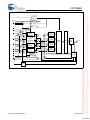
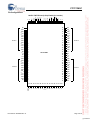
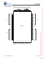
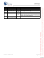
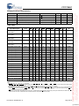
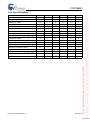
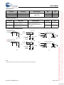
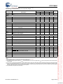
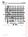
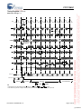
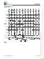
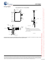
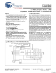
CY7C1365C
9-Mbit (256K x 32) Flow-Through Sync SRAM
Functional Description[1]
Features
• 256K x 32 common I/O
• 3.3V core power supply (VDD)
• 2.5V/3.3V I/O power supply (VDDQ)
• Fast clock-to-output times
— 6.5 ns (133-MHz version)
• Provide high-performance 2-1-1-1 access rate
• User-selectable burst counter supporting Intel®
Pentium® interleaved or linear burst sequences
• Separate processor and controller address strobes
• Synchronous self-timed write
• Asynchronous output enable
• Supports 3.3V I/O level
• Available in JEDEC-standard lead-free 100-Pin TQFP
package
• TQFP Available with 3-Chip Enable and 2-Chip Enable
• “ZZ” Sleep Mode option
The CY7C1365C is a 256K x 32 synchronous cache RAM
designed to interface with high-speed microprocessors with
minimum glue logic. Maximum access delay from clock rise is
6.5 ns (133-MHz version). A 2-bit on-chip counter captures the
first address in a burst and increments the address automatically for the rest of the burst access. All synchronous inputs
are gated by registers controlled by a positive-edge-triggered
Clock Input (CLK). The synchronous inputs include all
addresses, all data inputs, address-pipelining Chip Enable
(CE1), depth-expansion Chip Enables (CE2 and CE3[2]), Burst
Control inputs (ADSC, ADSP, and ADV), Write Enables
(BW[A:D], and BWE), and Global Write (GW). Asynchronous
inputs include the Output Enable (OE) and the ZZ pin.
The CY7C1365C allows either interleaved or linear burst
sequences, selected by the MODE input pin. A HIGH selects
an interleaved burst sequence, while a LOW selects a linear
burst sequence. Burst accesses can be initiated with the
Processor Address Strobe (ADSP) or the cache Controller
Address Strobe (ADSC) inputs. Address advancement is
controlled by the Address Advancement (ADV) input.
Addresses and Chip Enables are registered at rising edge of
clock when either Address Strobe Processor (ADSP) or
Address Strobe Controller (ADSC) are active. Subsequent
burst addresses can be internally generated as controlled by
the Advance pin (ADV).
The CY7C1365C operates from a +3.3V core power supply
while all outputs may operate with either a +2.5 or +3.3V
supply. All inputs and outputs are JEDEC-standard
JESD8-5-compatible.
Selection Guide
133 MHz
100 MHz
Unit
Maximum Access Time
6.5
8.5
ns
Maximum Operating Current
250
180
mA
Maximum Standby Current
40
40
mA
Notes:
1. For best-practices recommendations, please refer to the Cypress application note System Design Guidelines on www.cypress.com.
2. CE3 is not available on 2 Chip Enable TQFP package.
Cypress Semiconductor Corporation
Document #: 38-05690 Rev. *E
•
198 Champion Court
•
San Jose, CA 95134-1709
•
408-943-2600
Revised September 14, 2006
[+] Feedback
CY7C1365C
Logic Block Diagram-CY7C1365C (256K x 32)
ADDRESS
REGISTER
A0, A1, A
A[1:0]
MODE
BURST Q1
COUNTER
AND LOGIC
Q0
CLR
ADV
CLK
ADSC
ADSP
DQD
BWD
BYTE
WRITE REGISTER
DQC
BWC
BYTE
WRITE REGISTER
DQD
BYTE
WRITE REGISTER
DQC
BYTE
WRITE REGISTER
DQB
BWB
DQB
BYTE
BYTE
WRITE REGISTER
MEMORY
ARRAY
SENSE
AMPS
OUTPUT
BUFFERS
DQs
WRITE REGISTER
DQA
BWA
BWE
DQA
BYTE
BYTE
WRITE REGISTER
WRITE REGISTER
GW
ENABLE
REGISTER
CE1
CE2
INPUT
REGISTERS
CE3
OE
ZZ
SLEEP
CONTROL
Document #: 38-05690 Rev. *E
Page 2 of 18
[+] Feedback
CY7C1365C
Pin Configurations
Document #: 38-05690 Rev. *E
A
A
81
82
83
84
BWE
OE
ADSC
ADSP
ADV
85
86
GW
89
87
CLK
91
88
VDD
VSS
93
90
BWSA
A
94
92
BWSC
BWSB
95
CE2
BWSD
96
98
97
A
CE1
99
35
36
37
38
39
40
41
42
45
46
47
48
49
50
A1
A0
NC
NC
VSS
VDD
NC
NC
A
A
A
A
A
A
A
44
34
A
43
A
31
VSSQ
VDDQ
DQD
DQD
NC
A
VSS
DQD
DQD
VDDQ
VSSQ
DQD
DQD
DQD
DQD
CY7C1365C
33
BYTE D
DQC
DQC
VSSQ
VDDQ
DQC
DQC
NC
VDD
NC
A
BYTE C
80
79
78
77
76
75
74
73
72
71
70
69
68
67
66
65
64
63
62
61
60
59
58
57
56
55
54
53
52
51
32
VDDQ
VSSQ
DQC
DQC
1
2
3
4
5
6
7
8
9
10
11
12
13
14
15
16
17
18
19
20
21
22
23
24
25
26
27
28
29
30
MODE
A
NC
DQC
DQC
100
100-Pin TQFP Pinout (2 Chip Enable) (AJ version)
NC
DQB
DQB
VDDQ
VSSQ
DQB
DQB
DQB
DQB
VSSQ
VDDQ
DQB
DQB
VSS
NC
BYTE B
VDD
ZZ
DQA
DQA
VDDQ
VSSQ
DQA
DQA
DQA
DQA
BYTE A
VSSQ
VDDQ
DQA
DQA
NC
Page 3 of 18
[+] Feedback
CY7C1365C
Pin Configurations (continued)
Document #: 38-05690 Rev. *E
A
A
81
82
83
84
BWE
OE
ADSC
ADSP
ADV
85
86
GW
89
87
CLK
91
88
VDD
VSS
93
90
BWSA
CE3
94
92
BWSC
BWSB
95
CE2
BWSD
96
98
97
A
CE1
99
35
36
37
38
39
40
41
42
45
46
47
48
49
50
A1
A0
NC
NC
VSS
VDD
NC
A
A
A
A
A
A
A
A
44
34
A
43
A
31
VSSQ
VDDQ
DQD
DQD
NC
A
VSS
DQD
DQD
VDDQ
VSSQ
DQD
DQD
DQD
DQD
CY7C1365C
33
BYTE D
DQC
DQC
VSSQ
VDDQ
DQC
DQC
NC
VDD
NC
A
BYTE C
80
79
78
77
76
75
74
73
72
71
70
69
68
67
66
65
64
63
62
61
60
59
58
57
56
55
54
53
52
51
32
VDDQ
VSSQ
DQC
DQC
1
2
3
4
5
6
7
8
9
10
11
12
13
14
15
16
17
18
19
20
21
22
23
24
25
26
27
28
29
30
MODE
A
NC
DQC
DQC
100
100-Pin TQFP Pinout (3 Chip Enable) (A version)
NC
DQB
DQB
VDDQ
VSSQ
DQB
DQB
DQB
DQB
VSSQ
VDDQ
DQB
DQB
VSS
NC
BYTE B
VDD
ZZ
DQA
DQA
VDDQ
VSSQ
DQA
DQA
DQA
DQA
BYTE A
VSSQ
VDDQ
DQA
DQA
NC
Page 4 of 18
[+] Feedback
CY7C1365C
Pin Descriptions
Name
A0, A1, A
TQFP
I/O
Description
37,36,32,33,34,35,44,45,46,
InputAddress Inputs used to select one of the 256K address
47,48,49,50,81,82,99,100
Synchronous locations. Sampled at the rising edge of the CLK if ADSP or ADSC
92 (for 2 Chip Enable Version)
is active LOW, and CE1, CE2, and CE3 are sampled active. A[1:0] feed
43 (for 3 Chip Enable Version)
the 2-bit counter.
BWA, BWB, 93,94,
BWC, BWD 95,96
InputByte Write Select Inputs, active LOW. Qualified with BWE to
Synchronous conduct Byte Writes to the SRAM. Sampled on the rising edge of
CLK.
GW
88
InputGlobal Write Enable Input, active LOW. When asserted LOW on
Synchronous the rising edge of CLK, a global write is conducted (ALL bytes are
written, regardless of the values on BW[A:D] and BWE).
BWE
87
InputByte Write Enable Input, active LOW. Sampled on the rising edge
Synchronous of CLK. This signal must be asserted LOW to conduct a Byte Write.
CLK
89
CE1
98
InputChip Enable 1 Input, active LOW. Sampled on the rising edge of
Synchronous CLK. Used in conjunction with CE2 and CE3 to select/deselect the
device. ADSP is ignored if CE1 is HIGH. CE1 is sampled only when
a new external address is loaded.
CE2
97
InputChip Enable 2 Input, active HIGH. Sampled on the rising edge of
Synchronous CLK. Used in conjunction with CE1 and CE3 to select/deselect the
device. CE2 is sampled only when a new external address is loaded.
CE3
92 (for 3 Chip Enable Version)
InputChip Enable 3 Input, active LOW. Sampled on the rising edge of
Synchronous CLK. Used in conjunction with CE1 and CE2 to select/deselect the
device. CE3 is assumed active throughout this document for BGA.
CE3 is sampled only when a new external address is loaded.
OE
86
InputOutput Enable, asynchronous input, active LOW. Controls the
Asynchronous direction of the I/O pins. When LOW, the I/O pins behave as outputs.
When deasserted HIGH, I/O pins are tri-stated, and act as input data
pins. OE is masked during the first clock of a Read cycle when
emerging from a deselected state.
ADV
83
InputAdvance Input signal, sampled on the rising edge of CLK. When
Synchronous asserted, it automatically increments the address in a burst cycle.
ADSP
84
InputAddress Strobe from Processor, sampled on the rising edge of
Synchronous CLK, active LOW. When asserted LOW, addresses presented to the
device are captured in the address registers. A[1:0] are also loaded
into the burst counter. When ADSP and ADSC are both asserted,
only ADSP is recognized. ASDP is ignored when CE1 is deasserted
HIGH.
ADSC
85
InputAddress Strobe from Controller, sampled on the rising edge of
Synchronous CLK, active LOW. When asserted LOW, addresses presented to the
device are captured in the address registers. A[1:0] are also loaded
into the burst counter. When ADSP and ADSC are both asserted,
only ADSP is recognized.
ZZ
64
InputZZ “sleep” Input, active HIGH. When asserted HIGH places the
Asynchronous device in a non-time-critical “sleep” condition with data integrity
preserved. For normal operation, this pin has to be LOW or left
floating. ZZ pin has an internal pull-down.
DQs
52,53,56, 57,58,59, 62,63,68,
I/OBidirectional Data I/O lines. As inputs, they feed into an on-chip
69,72,73,74,75,78,79,2,3,6,7, Synchronous data register that is triggered by the rising edge of CLK. As outputs,
8,9,12,13,18,19,22,23,24,25,
they deliver the data contained in the memory location specified by
28,29
the addresses presented during the previous clock rise of the read
cycle. The direction of the pins is controlled by OE. When OE is
asserted LOW, the pins behave as outputs. When HIGH, DQs are
placed in a tri-state condition.
Document #: 38-05690 Rev. *E
Input-Clock
Clock Input. Used to capture all synchronous inputs to the device.
Also used to increment the burst counter when ADV is asserted LOW,
during a burst operation.
Page 5 of 18
[+] Feedback
CY7C1365C
Pin Descriptions (continued)
Name
TQFP
I/O
Description
VDD
15,41,65, 91
VSS
17,40,67,90
Ground
Ground for the core of the device.
VDDQ
4,11,20,27,54,61,70,77,
I/O Power
Supply
Power supply for the I/O circuitry.
VSSQ
5,10,21,26,55,60,71,76
I/O Ground
Ground for the I/O circuitry.
MODE
31
NC
1,30,51,80,14,16,38,39,42,66
43 (for 2 Chip Enable Version)
Document #: 38-05690 Rev. *E
Power Supply Power supply inputs to the core of the device.
InputStatic
Selects Burst Order. When tied to GND selects linear burst
sequence. When tied to VDD or left floating selects interleaved burst
sequence. This is a strap pin and should remain static during device
operation. Mode Pin has an internal pull-up.
No Connects. Not Internally connected to the die.
Page 6 of 18
[+] Feedback
CY7C1365C
Functional Overview
All synchronous inputs pass through input registers controlled
by the rising edge of the clock. Maximum access delay from
the clock rise (t CDV) is 6.5 ns (133-MHz device).
The CY7C1365C supports secondary cache in systems
utilizing either a linear or interleaved burst sequence. The
interleaved burst order supports Pentium and i486 processors.
The linear burst sequence is suited for processors that utilize
a linear burst sequence. The burst order is user-selectable,
and is determined by sampling the MODE input. Accesses can
be initiated with either the Processor Address Strobe (ADSP)
or the Controller Address Strobe (ADSC). Address
advancement through the burst sequence is controlled by the
ADV input. A two-bit on-chip wraparound burst counter
captures the first address in a burst sequence and automatically increments the address for the rest of the burst access.
Byte write operations are qualified with the Byte Write Enable
(BWE) and Byte Write Select (BW[A:D]) inputs. A Global Write
Enable (GW) overrides all byte write inputs and writes data to
all four bytes. All writes are simplified with on-chip
synchronous self-timed write circuitry.
Three synchronous Chip Selects (CE1, CE2, CE3) and an
asynchronous Output Enable (OE) provide for easy bank
selection and output tri-state control. ADSP is ignored if CE1
is HIGH.
Single Read Accesses
A single read access is initiated when the following conditions
are satisfied at clock rise: (1) CE1, CE2, and CE3 are all
asserted active, and (2) ADSP or ADSC is asserted LOW (if
the access is initiated by ADSC, the write inputs must be
deasserted during this first cycle). The address presented to
the address inputs is latched into the address register and the
burst counter/control logic and presented to the memory core.
If the OE input is asserted LOW, the requested data will be
available at the data outputs a maximum to tCDV after clock
rise. ADSP is ignored if CE1 is HIGH.
Single Write Accesses Initiated by ADSP
This access is initiated when the following conditions are
satisfied at clock rise: (1) CE1, CE2, CE3 are all asserted
active, and (2) ADSP is asserted LOW. The addresses
presented are loaded into the address register and the burst
inputs (GW, BWE, and BW[A:D]) are ignored during this first
clock cycle. If the write inputs are asserted active (see Write
Cycle Descriptions table for appropriate states that indicate a
write) on the next clock rise, the appropriate data will be
latched and written into the device.Byte writes are allowed.
During byte writes, BWA controls DQA and BWB controls
DQB, BWC controls DQC, and BWD controls DQD. All I/Os
are tri-stated during a byte write.Since this is a common I/O
device, the asynchronous OE input signal must be deasserted
and the I/Os must be tri-stated prior to the presentation of data
to DQs. As a safety precaution, the data lines are tri-stated
once a write cycle is detected, regardless of the state of OE.
active, (2) ADSC is asserted LOW, (3) ADSP is deasserted
HIGH, and (4) the write input signals (GW, BWE, and BW[A:D])
indicate a write access. ADSC is ignored if ADSP is active
LOW.
The addresses presented are loaded into the address register
and the burst counter/control logic and delivered to the
memory core. The information presented to DQ[D:A] will be
written into the specified address location. Byte writes are
allowed. During byte writes, BWA controls DQA, BWB controls
DQB, BWC controls DQC, and BWD controls DQD. All I/Os
are tri-stated when a write is detected, even a byte write. Since
this is a common I/O device, the asynchronous OE input signal
must be deasserted and the I/Os must be tri-stated prior to the
presentation of data to DQs. As a safety precaution, the data
lines are tri-stated once a write cycle is detected, regardless
of the state of OE.
Burst Sequences
The CY7C1365C provides an on-chip two-bit wraparound
burst counter inside the SRAM. The burst counter is fed by
A[1:0], and can follow either a linear or interleaved burst order.
The burst order is determined by the state of the MODE input.
A LOW on MODE will select a linear burst sequence. A HIGH
on MODE will select an interleaved burst order. Leaving
MODE unconnected will cause the device to default to a interleaved burst sequence.
Sleep Mode
The ZZ input pin is an asynchronous input. Asserting ZZ
places the SRAM in a power conservation “sleep” mode. Two
clock cycles are required to enter into or exit from this “sleep”
mode. While in this mode, data integrity is guaranteed.
Accesses pending when entering the “sleep” mode are not
considered valid nor is the completion of the operation
guaranteed. The device must be deselected prior to entering
the “sleep” mode. CEs, ADSP, and ADSC must remain
inactive for the duration of tZZREC after the ZZ input returns
LOW.
Interleaved Burst Address Table
(MODE = Floating or VDD)
First
Address
A1, A0
Second
Address
A1, A0
Third
Address
A1, A0
Fourth
Address
A1, A0
00
01
10
11
01
00
11
10
10
11
00
01
11
10
01
00
Linear Burst Address Table (MODE = GND)
First
Address
A1, A0
Second
Address
A1, A0
Third
Address
A1, A0
Fourth
Address
A1, A0
10
11
00
01
Single Write Accesses Initiated by ADSC
01
10
11
00
This write access is initiated when the following conditions are
satisfied at clock rise: (1) CE1, CE2, and CE3 are all asserted
10
11
00
01
11
00
01
10
Document #: 38-05690 Rev. *E
Page 7 of 18
[+] Feedback
CY7C1365C
ZZ Mode Electrical Characteristics
Parameter
Description
Test Conditions
IDDZZ
Sleep mode standby current
ZZ > VDD – 0.2V
Min.
tZZS
Device operation to ZZ
ZZ > VDD – 0.2V
tZZREC
ZZ recovery time
ZZ < 0.2V
tZZI
ZZ Active to Sleep current
This parameter is sampled
tRZZI
ZZ Inactive to exit Sleep current
This parameter is sampled
Max.
Unit
50
mA
2tCYC
ns
2tCYC
ns
2tCYC
0
ns
ns
Truth Table[3, 4, 5, 6, 7]
Cycle Description
Address
Used
ADSP
ADSC
ADV
WRITE
OE
CLK
DQ
Deselected Cycle,
Power-down
None
CE1 CE3 CE2 ZZ
H
X
X
L
X
L
X
X
X
L-H
Tri-State
Deselected Cycle,
Power-down
None
L
X
L
L
L
X
X
X
X
L-H
Tri-State
Deselected Cycle,
Power-down
None
L
H
X
L
L
X
X
X
X
L-H
Tri-State
Deselected Cycle,
Power-down
None
L
X
L
L
H
L
X
X
X
L-H
Tri-State
Deselected Cycle,
Power-down
None
X
X
X
L
H
L
X
X
X
L-H
Tri-State
Sleep Mode, Power-down
None
X
X
X
H
X
X
X
X
X
X
Tri-State
Read Cycle, Begin Burst
External
L
L
H
L
L
X
X
X
L
L-H
Q
Read Cycle, Begin Burst
External
L
L
H
L
L
X
X
X
H
L-H
Tri-State
Write Cycle, Begin Burst
External
L
L
H
L
H
L
X
L
X
L-H
D
Read Cycle, Begin Burst
External
L
L
H
L
H
L
X
H
L
L-H
Q
Read Cycle, Begin Burst
External
L
L
H
L
H
L
X
H
H
L-H
Tri-State
Next
X
X
X
L
H
H
L
H
L
L-H
Q
Read Cycle, Continue Burst
Read Cycle, Continue Burst
Next
X
X
X
L
H
H
L
H
H
L-H
Tri-State
Read Cycle, Continue Burst
Next
H
X
X
L
X
H
L
H
L
L-H
Q
Read Cycle, Continue Burst
Next
H
X
X
L
X
H
L
H
H
L-H
Tri-State
Write Cycle, Continue Burst
Next
X
X
X
L
H
H
L
L
X
L-H
D
Write Cycle, Continue Burst
Next
H
X
X
L
X
H
L
L
X
L-H
D
Read Cycle, Suspend Burst
Current
X
X
X
L
H
H
H
H
L
L-H
Q
Read Cycle, Suspend Burst
Current
X
X
X
L
H
H
H
H
H
L-H
Tri-State
Read Cycle, Suspend Burst
Current
H
X
X
L
X
H
H
H
L
L-H
Q
Read Cycle, Suspend Burst
Current
H
X
X
L
X
H
H
H
H
L-H
Tri-State
Write Cycle, Suspend Burst
Current
X
X
X
L
H
H
H
L
X
L-H
D
Write Cycle, Suspend Burst
Current
H
X
X
L
X
H
H
L
X
L-H
D
Notes:
3. X = “Don't Care.” H = Logic HIGH, L = Logic LOW.
4. WRITE = L when any one or more Byte Write Enable signals (BWA, BWB, BWC, BWD) and BWE = L or GW = L. WRITE = H when all Byte Write Enable signals
(BWA, BWB, BWC, BWD), BWE, GW = H.
5. The DQ pins are controlled by the current cycle and the OE signal. OE is asynchronous and is not sampled with the clock.
6. The SRAM always initiates a Read cycle when ADSP is asserted, regardless of the state of GW, BWE, or BW[A: D]. Writes may occur only on subsequent clocks
after the ADSP or with the assertion of ADSC. As a result, OE must be driven HIGH prior to the start of the write cycle to allow the outputs to tri-state. OE is a
don't care for the remainder of the Write cycle.
7. OE is asynchronous and is not sampled with the clock rise. It is masked internally during Write cycles. During a read cycle all data bits are Tri-State when OE is
inactive or when the device is deselected, and all data bits behave as output when OE is active (LOW).
Document #: 38-05690 Rev. *E
Page 8 of 18
[+] Feedback
CY7C1365C
Truth Table for Read/Write[3, 4]
GW
BWE
BWD
BWC
BWB
BWA
Read
Function
H
H
X
X
X
X
Read
H
L
H
H
H
H
Write Byte (A, DQPA)
H
L
H
H
H
L
Write Byte (B, DQPB)
H
L
H
H
L
H
Write Bytes (B, A, DQPA, DQPB)
H
L
H
H
L
L
Write Byte (C, DQPC)
H
L
H
L
H
H
Write Bytes (C, A, DQPC, DQPA)
H
L
H
L
H
L
Write Bytes (C, B, DQPC, DQPB)
H
L
H
L
L
H
Write Bytes (C, B, A, DQPC, DQPB, DQPA)
H
L
H
L
L
L
Write Byte (D, DQPD)
H
L
L
H
H
H
Write Bytes (D, A, DQPD, DQPA)
H
L
L
H
H
L
Write Bytes (D, B, DQPD, DQPA)
H
L
L
H
L
H
Write Bytes (D, B, A, DQPD, DQPB, DQPA)
H
L
L
H
L
L
Write Bytes (D, B, DQPD, DQPB)
H
L
L
L
H
H
Write Bytes (D, B, A, DQPD, DQPC, DQPA)
H
L
L
L
H
L
Write Bytes (D, C, A, DQPD, DQPB, DQPA)
H
L
L
L
L
H
Write All Bytes
H
L
L
L
L
L
Write All Bytes
L
X
X
X
X
X
Document #: 38-05690 Rev. *E
Page 9 of 18
[+] Feedback
CY7C1365C
Maximum Ratings
DC Input Voltage ................................... –0.5V to VDD + 0.5V
Current into Outputs (LOW)......................................... 20 mA
(Above which the useful life may be impaired. For user guidelines, not tested.)
Static Discharge Voltage........................................... >2001V
(per MIL-STD-883, Method 3015)
Storage Temperature ................................. –65°C to +150°C
Latch-up Current..................................................... >200 mA
Ambient Temperature with
Power Applied............................................. –55°C to +125°C
Operating Range
Supply Voltage on VDD Relative to GND........ –0.5V to +4.6V
Ambient
Temperature
Range
Supply Voltage on VDDQ Relative to GND ...... –0.5V to +VDD
Commercial
DC Voltage Applied to Outputs
in Tri-State........................................... –0.5V to VDDQ + 0.5V
Industrial
0°C to +70°C
–40°C to +85°C
VDD
VDDQ
3.3V –
5%/+10%
2.5V – 5% to
VDD
Electrical Characteristics Over the Operating Range [8, 9]
CY7C1365C
Parameter
Description
Test Conditions
Min.
Max.
Unit
VDD
Power Supply Voltage
VDDQ
I/O Supply Voltage
VOH
Output HIGH Voltage
VOL
Output LOW Voltage
VIH
Input HIGH Voltage
VIL
Input LOW Voltage[8]
IX
Input Leakage Current
except ZZ and MODE
GND ≤ VI ≤ VDDQ
Input Current of MODE
Input = VSS
–30
Input Current of ZZ
Input = VSS
3.135
3.6
V
for 3.3V I/O
3.135
3.6
V
for 2.5V I/O
2.375
2.625
for 3.3V I/O, IOH = –4.0 mA
2.4
for 2.5V I/O, IOH = –1.0 mA
2.0
for 3.3V I/O, IOL = 8.0 mA
for 2.5V I/O, IOL = 1.0 mA
V
V
V
0.4
V
0.4
V
2.0
VDD + 0.3V
V
for 2.5V I/O
1.7
VDD + 0.3V
V
for 3.3V I/O
–0.3
0.8
V
for 2.5V I/O
–0.3
0.7
V
−5
5
µA
for 3.3V I/O
Input = VDD
5
GND ≤ VI ≤ VDDQ, Output Disabled
Output Leakage Current
IDD
VDD Operating Supply Current VDD = Max., IOUT = 0 mA,
f = fMAX= 1/tCYC
–5
µA
µA
–5
Input = VDD
IOZ
µA
30
µA
5
µA
7.5-ns cycle, 133 MHz
250
mA
10-ns cycle, 100 MHz
180
mA
ISB1
Automatic CE Power-Down
Current—TTL Inputs
Max. VDD, Device Deselected, All speeds
VIN ≥ VIH or VIN ≤ VIL, f = fMAX,
inputs switching
110
mA
ISB2
Automatic CE Power-Down
Current—CMOS Inputs
Max. VDD, Device Deselected,
All speeds
VIN ≥ VDD – 0.3V or VIN ≤ 0.3V,
f = 0, inputs static
40
mA
ISB3
Automatic CE Power-Down
Current—CMOS Inputs
All speeds
Max. VDD, Device Deselected,
VIN ≥ VDDQ – 0.3V or VIN ≤ 0.3V,
f = fMAX, inputs switching
100
mA
ISB4
Automatic CE Power-Down
Current—TTL Inputs
Max. VDD, Device Deselected, All speeds
VIN ≥ VIH or VIN ≤ VIL, f = 0,
inputs static.
40
mA
Notes:
8. Overshoot: VIH(AC) < VDD +1.5V (Pulse width less than tCYC/2), undershoot: VIL(AC) > –2V (Pulse width less than tCYC/2).
9. TPower-up: Assumes a linear ramp from 0V to VDD(min.) within 200 ms. During this time VIH < VDD and VDDQ < VDD.
Document #: 38-05690 Rev. *E
Page 10 of 18
[+] Feedback
CY7C1365C
Capacitance[10]
Parameter
Description
CIN
Input Capacitance
CCLK
Clock Input Capacitance
CI/O
Input/Output Capacitance
Test Conditions
100 TQFP
Max.
TA = 25°C, f = 1 MHz,
VDD = 3.3V
VDDQ = 2.5V
5
pF
5
pF
5
pF
Unit
Thermal Resistance[10]
Parameter
Description
ΘJA
Thermal Resistance
(Junction to Ambient)
ΘJC
Thermal Resistance
(Junction to Case)
Test Conditions
Test conditions follow standard test
methods and procedures for
measuring thermal impedance, per
EIA/JESD51
100 TQFP
Package
Unit
29.41
°C/W
6.13
°C/W
AC Test Loads and Waveforms
3.3V I/O Test Load
R = 317Ω
3.3V
OUTPUT
Z0 = 50Ω
10%
INCLUDING
JIG AND
SCOPE
2.5V I/O Test Load
R = 351Ω
(b)
(c)
10%
(a)
90%
10%
90%
GND
5 pF
VT = 1.25V
ALL INPUT PULSES
VDDQ
OUTPUT
RL = 50Ω
Z0 = 50Ω
≤ 1 ns
≤ 1 ns
R = 1667Ω
2.5V
OUTPUT
90%
10%
90%
GND
5 pF
VT = 1.5V
(a)
ALL INPUT PULSES
VDDQ
OUTPUT
RL = 50Ω
R =1538Ω
INCLUDING
JIG AND
SCOPE
(b)
≤ 1 ns
≤ 1 ns
(c)
Notes:
10. Tested initially and after any design or process change that may affect these parameters.
Document #: 38-05690 Rev. *E
Page 11 of 18
[+] Feedback
CY7C1365C
Switching Characteristics Over the Operating Range[11, 12]
–133
Parameter
tPOWER
Description
VDD(Typical) to the First Access
[13]
Min.
–100
Max.
Min.
Max.
Unit
1
1
ms
Clock
tCYC
Clock Cycle Time
7.5
10
ns
tCH
Clock HIGH
3.0
4.0
ns
tCL
Clock LOW
3.0
4.0
ns
Output Times
tCDV
Data Output Valid after CLK Rise
tDOH
Data Output Hold after CLK Rise
[14, 15, 16]
6.5
2.0
8.5
2.0
ns
tCLZ
Clock to Low-Z
tCHZ
Clock to High-Z[14, 15, 16]
3.5
3.5
ns
tOEV
OE LOW to Output Valid
3.5
3.5
ns
tOELZ
tOEHZ
OE LOW to Output
Low-Z[14, 15, 16]
OE HIGH to Output
High-Z[14, 15, 16]
0
ns
0
0
ns
0
3.5
ns
3.5
ns
Set-up Times
tAS
Address Set-up before CLK Rise
1.5
1.5
ns
tADS
ADSP, ADSC Set-up before CLK Rise
1.5
1.5
ns
tADVS
ADV Set-up before CLK Rise
1.5
1.5
ns
tWES
GW, BWE, BW[A:D] Set-up before CLK Rise
1.5
1.5
ns
tDS
Data Input Set-up before CLK Rise
1.5
1.5
ns
tCES
Chip Enable Set-up
1.5
1.5
ns
tAH
Address Hold after CLK Rise
0.5
0.5
ns
tADH
ADSP, ADSC Hold after CLK Rise
0.5
0.5
ns
tWEH
GW,BWE, BW[A:D] Hold after CLK Rise
0.5
0.5
ns
tADVH
ADV Hold after CLK Rise
0.5
0.5
ns
tDH
Data Input Hold after CLK Rise
0.5
0.5
ns
tCEH
Chip Enable Hold after CLK Rise
0.5
0.5
ns
Hold Times
Notes:
11. Timing reference level is 1.5V when VDDQ = 3.3V and is 1.25V when VDDQ = 2.5V.
12. Test conditions shown in (a) of AC Test Loads unless otherwise noted.
13. This part has a voltage regulator internally; tPOWER is the time that the power needs to be supplied above VDD(minimum) initially before a Read or Write operation
can be initiated.
14. tCHZ, tCLZ,tOELZ, and tOEHZ are specified with AC test conditions shown in part (b) of AC Test Loads. Transition is measured ± 200 mV from steady-state voltage.
15. At any given voltage and temperature, tOEHZ is less than tOELZ and tCHZ is less than tCLZ to eliminate bus contention between SRAMs when sharing the same
data bus. These specifications do not imply a bus contention condition, but reflect parameters guaranteed over worst case user conditions. Device is designed
to achieve High-Z prior to Low-Z under the same system conditions.
16. This parameter is sampled and not 100% tested.
Document #: 38-05690 Rev. *E
Page 12 of 18
[+] Feedback
CY7C1365C
Timing Diagrams
Read Cycle Timing[17]
tCYC
CLK
t
tADS
CH
t CL
tADH
ADSP
tADS
tADH
ADSC
tAS
tAH
A1
ADDRESS
A2
t
WES
t
WEH
GW, BWE,BW
[A:D]
tCES
Deselect Cycle
t CEH
CE
t
ADVS
t
ADVH
ADV
ADV suspends burst.
OE
t OEV
t OEHZ
t CLZ
Data Out (Q)
High-Z
Q(A1)
t OELZ
tCDV
t CHZ
tDOH
Q(A2)
Q(A2 + 1)
Q(A2 + 2)
Q(A2 + 3)
Q(A2)
Q(A2 + 1)
Q(A2 + 2)
t CDV
Single READ
BURST
READ
DON’T CARE
Burst wraps around
to its initial state
UNDEFINED
Note:
17. On this diagram, when CE is LOW, CE1 is LOW, CE2 is HIGH and CE3 is LOW. When CE is HIGH, CE1 is HIGH or CE2 is LOW or CE3 is HIGH.
Document #: 38-05690 Rev. *E
Page 13 of 18
[+] Feedback
CY7C1365C
Timing Diagrams (continued)
Write Cycle Timing[18, 19]
t CYC
CLK
t
tADS
t
CH
CL
tADH
ADSP
tADS
ADSC extends burst.
tADH
tADS
tADH
ADSC
tAS
tAH
A1
ADDRESS
A2
A3
Byte write signals are ignored for first cycle when
ADSP initiates burst.
tWES tWEH
BWE,
BW[A:D]
t
t
WES WEH
GW
tCES
tCEH
CE
tADVS tADVH
ADV
ADV suspends burst.
OE
t
Data in (D)
High-Z
t
OEHZ
t
DS DH
D(A1)
D(A2)
D(A2 + 1)
D(A2 + 1)
D(A2 + 2)
D(A2 + 3)
D(A3)
D(A3 + 1)
D(A3 + 2)
Data Out (Q)
BURST READ
Single WRITE
BURST WRITE
DON’T CARE
Extended BURST WRITE
UNDEFINED
Notes:
18. Full width write can be initiated by either GW LOW; or by GW HIGH, BWE LOW and BW[A:D] LOW.
19. The data bus (Q) remains in High-Z following a Write cycle unless an ADSP, ADSC, or ADV cycle is performed.
Document #: 38-05690 Rev. *E
Page 14 of 18
[+] Feedback
CY7C1365C
Timing Diagrams (continued)
Read/Write Timing[17, 19, 20]
tCYC
CLK
t
CH
tADS
tADH
tAS
tAH
t
CL
ADSP
ADSC
ADDRESS
A1
A2
A3
A4
A5
A6
D(A5)
D(A6)
t
t
WES WEH
BWE, BW[A:D]
tCES
tCEH
CE
ADV
OE
tDS
Data In (D)
Data Out (Q)
High-Z
t
OEHZ
Q(A1)
tDH
tOELZ
D(A3)
tCDV
Q(A2)
Back-to-Back READs
Q(A4)
Single WRITE
Q(A4+1)
Q(A4+2)
BURST READ
DON’T CARE
Q(A4+3)
Back-to-Back
WRITEs
UNDEFINED
Note:
20. GW is HIGH.
Document #: 38-05690 Rev. *E
Page 15 of 18
[+] Feedback
CY7C1365C
Timing Diagrams (continued)
ZZ Mode Timing [21, 22]
CLK
t ZZ
ZZ
I
t ZZREC
t ZZI
SUPPLY
I DDZZ
t RZZI
ALL INPUTS
(except ZZ)
DESELECT or READ Only
Outputs (Q)
High-Z
DON’T CARE
Ordering Information
Not all of the speed, package and temperature ranges are available. Please contact your local sales representative or
visit www.cypress.com for actual products offered.
Speed
(MHz)
133
100
Ordering Code
CY7C1365C-133AXC
Package
Diagram
Package Type
51-85050 100-pin Thin Quad Flat Pack (14 x 20 x 1.4 mm) Lead-Free Commercial
(3 Chip Enable)
CY7C1365C-133AJXC
100-pin Thin Quad Flat Pack (14 x 20 x 1.4 mm) Lead-Free
(2 Chip Enable)
CY7C1365C-133AXI
100-pin Thin Quad Flat Pack (14 x 20 x 1.4 mm) Lead-Free
(3 Chip Enable)
CY7C1365C-133AJXI
100-pin Thin Quad Flat Pack (14 x 20 x 1.4 mm) Lead-Free
(2 Chip Enable)
CY7C1365C-100AXC
Operating
Range
Industrial
51-85050 100-pin Thin Quad Flat Pack (14 x 20 x 1.4 mm) Lead-Free Commercial
(3 Chip Enable)
CY7C1365C-100AJXC
100-pin Thin Quad Flat Pack (14 x 20 x 1.4 mm) Lead-Free
(2 Chip Enable)
CY7C1365C-100AXI
100-pin Thin Quad Flat Pack (14 x 20 x 1.4 mm) Lead-Free
(3 Chip Enable)
CY7C1365C-100AJXI
100-pin Thin Quad Flat Pack (14 x 20 x 1.4 mm) Lead-Free
(2 Chip Enable)
Industrial
Notes:
21. Device must be deselected when entering ZZ mode. See Cycle Descriptions table for all possible signal conditions to deselect the device.
22. DQs are in High-Z when exiting ZZ sleep mode.
Document #: 38-05690 Rev. *E
Page 16 of 18
[+] Feedback
CY7C1365C
Package Diagram
100-Pin TQFP (14 x 20 x 1.4 mm) (51-85050)
16.00±0.20
1.40±0.05
14.00±0.10
100
81
80
1
20.00±0.10
22.00±0.20
0.30±0.08
0.65
TYP.
30
12°±1°
(8X)
SEE DETAIL
A
51
31
50
0.20 MAX.
0.10
1.60 MAX.
R 0.08 MIN.
0.20 MAX.
0° MIN.
SEATING PLANE
STAND-OFF
0.05 MIN.
0.15 MAX.
0.25
NOTE:
1. JEDEC STD REF MS-026
GAUGE PLANE
0°-7°
R 0.08 MIN.
0.20 MAX.
2. BODY LENGTH DIMENSION DOES NOT INCLUDE MOLD PROTRUSION/END FLASH
MOLD PROTRUSION/END FLASH SHALL NOT EXCEED 0.0098 in (0.25 mm) PER SIDE
BODY LENGTH DIMENSIONS ARE MAX PLASTIC BODY SIZE INCLUDING MOLD MISMATCH
3. DIMENSIONS IN MILLIMETERS
0.60±0.15
0.20 MIN.
51-85050-*B
1.00 REF.
DETAIL
A
Intel and Pentium are registered trademarks and i486 is a trademark of Intel Corporation. All product and company names
mentioned in this document may be the trademarks of their respective holders.
Document #: 38-05690 Rev. *E
Page 17 of 18
© Cypress Semiconductor Corporation, 2006. The information contained herein is subject to change without notice. Cypress Semiconductor Corporation assumes no responsibility for the use
of any circuitry other than circuitry embodied in a Cypress product. Nor does it convey or imply any license under patent or other rights. Cypress products are not warranted nor intended to be
used for medical, life support, life saving, critical control or safety applications, unless pursuant to an express written agreement with Cypress. Furthermore, Cypress does not authorize its
products for use as critical components in life-support systems where a malfunction or failure may reasonably be expected to result in significant injury to the user. The inclusion of Cypress
products in life-support systems application implies that the manufacturer assumes all risk of such use and in doing so indemnifies Cypress against all charges.
[+] Feedback
CY7C1365C
Document History Page
Document Title: CY7C1365C 9-Mbit (256K x 32) Flow-Through Sync SRAM
Document Number: 38-05690
REV.
ECN NO.
Issue Date
Orig. of
Change
Description of Change
**
286269
See ECN
PCI
New data sheet
*A
320834
See ECN
PCI
Added 133 MHz in the Ordering Information table
Changed ΘJA and ΘJC for TQFP Package from 25 and 9 °C/W to 29.41 and
6.13 °C/W respectively
Modified VOL, VOH test conditions
Corrected IDD, tCDV, tCH, tDOH and tCL for 100MHz to 180 mA, 8.5 ns, 4
ns, 2 ns and 4 ns respectively
Changed Snooze to Sleep in the ZZ Mode Electrical Characteristics and truth
table on page# 6
Added Industrial operating range
Updated Ordering Information Table
*B
377095
See ECN
PCI
Changed ISB2 from 30 to 40 mA
Modified test condition in note# 9 from VIH < VDD to VIH < VDD
*C
408725
See ECN
RXU
Changed address of Cypress Semiconductor Corporation on Page# 1 from
“3901 North First Street” to “198 Champion Court”
Changed three state to tri-state
Converted from Preliminary to Final
Modified “Input Load” to “Input Leakage Current except ZZ and MODE” in the
Electrical Characteristics Table
Replaced Package Name column with Package Diagram in the Ordering
Information table
Updated the ordering information
*D
429278
See ECN
NXR
Added 2.5VI/O option
Updated Ordering Information Table
*E
501828
See ECN
VKN
Added the Maximum Rating for Supply Voltage on VDDQ Relative to GND
Updated the Ordering Information table.
Document #: 38-05690 Rev. *E
Page 18 of 18
[+] Feedback