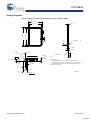
1
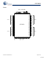
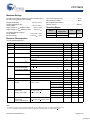
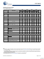
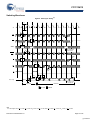
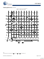
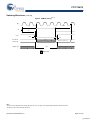
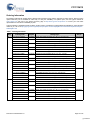
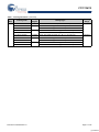
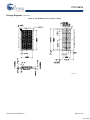
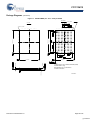
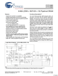
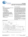
CY7C1347G
4-Mbit (128K x 36) Pipelined Sync SRAM
Features
Functional Description[1]
■
Fully registered inputs and outputs for pipelined operation
■
128K x 36 common IO architecture
■
3.3V core power supply (VDD)
■
2.5V/3.3V IO power supply (VDDQ)
■
Fast clock to output times: 2.6 ns (for 250 MHz device)
■
User-selectable burst counter supporting Intel® Pentium®
interleaved or linear burst sequences
■
Separate processor and controller address strobes
■
Synchronous self-timed writes
■
Asynchronous output enable
■
Offered in Pb-free 100-Pin TQFP, Pb-free and non Pb-free
119-Ball BGA package, and 165-Ball FBGA package
■
“ZZ” sleep mode option and stop clock option
The CY7C1347G is a 3.3V, 128K x 36 synchronous-pipelined
SRAM designed to support zero-wait-state secondary cache
with minimal glue logic. CY7C1347G IO pins can operate at
either the 2.5V or the 3.3V level. The IO pins are 3.3V tolerant
when VDDQ = 2.5V. All synchronous inputs pass through input
registers controlled by the rising edge of the clock. All data
outputs pass through output registers controlled by the rising
edge of the clock. Maximum access delay from the clock rise is
2.6 ns (250 MHz device). CY7C1347G supports either the
interleaved burst sequence used by the Intel Pentium processor
or a linear burst sequence used by processors such as the
PowerPC®. The burst sequence is selected through the MODE
pin. Accesses can be initiated by asserting either the Address
Strobe from Processor (ADSP) or the Address Strobe from
Controller (ADSC) at clock rise. Address advancement through
the burst sequence is controlled by the ADV input. A 2-bit on-chip
wraparound burst counter captures the first address in a burst
sequence and automatically increments the address for the rest
of the burst access.
■
Available in industrial and commercial temperature ranges
Byte write operations are qualified with the four Byte Write Select
(BW[A:D]) inputs. A Global Write Enable (GW) overrides all byte
write inputs and writes data to all four bytes. All writes are
conducted with on-chip synchronous self-timed write circuitry.
Three synchronous Chip Selects (CE1, CE2, CE3) and an
asynchronous Output Enable (OE) provide for easy bank
selection and output tri-state control. To provide proper data
during depth expansion, OE is masked during the first clock of a
read cycle when emerging from a deselected state.
Selection Guide
Specification
250 MHz
200 MHz
166 MHz
133 MHz
Unit
Maximum Access Time
2.6
2.8
3.5
4.0
ns
Maximum Operating Current
325
265
240
225
mA
Maximum CMOS Standby Current
40
40
40
40
mA
Note
1. For best practice recommendations, refer to the Cypress application note AN1064, SRAM System Guidelines.
Cypress Semiconductor Corporation
Document #: 38-05516 Rev. *F
•
198 Champion Court
•
San Jose, CA 95134-1709
•
408-943-2600
Revised January 15, 2009
[+] Feedback
CY7C1347G
Block Diagram
A0, A1, A
ADDRESS
REGISTER
2
A [1:0]
MODE
ADV
CLK
Q1
BURST
COUNTER
CLR AND
LOGIC
ADSC
Q0
ADSP
BW D
DQ D ,DQP D
BYTE
WRITE REGISTER
DQ D ,DQPD
BYTE
WRITE DRIVER
BW C
DQ C ,DQP C
BYTE
WRITE REGISTER
DQ C ,DQP C
BYTE
WRITE DRIVER
DQ B ,DQP B
BYTE
WRITE REGISTER
DQ B ,DQP B
BYTE
WRITE DRIVER
BW B
BW A
BWE
ZZ
ENABLE
REGISTER
SENSE
AMPS
OUTPUT
REGISTERS
OUTPUT
BUFFERS
E
DQs
DQP A
DQP B
DQP C
DQP D
DQ A ,DQP A
BYTE
WRITE DRIVER
DQ A ,DQP A
BYTE
WRITE REGISTER
GW
CE 1
CE 2
CE 3
OE
MEMORY
ARRAY
PIPELINED
ENABLE
INPUT
REGISTERS
SLEEP
CONTROL
Document #: 38-05516 Rev. *F
Page 2 of 22
[+] Feedback
CY7C1347G
Pinouts
100
99
98
97
96
95
94
93
92
91
90
89
88
87
86
85
84
83
82
81
A
A
CE1
CE2
BWD
BWC
BWB
BWA
CE3
VDD
VSS
CLK
GW
BWE
OE
ADSC
ADSP
ADV
A
A
Figure 1. 100-Pin TQFP
BYTE C
1
2
3
4
5
6
7
8
9
10
11
12
13
14
15
16
17
18
19
20
21
22
23
24
25
26
27
28
29
30
CY7C1347G
80
79
78
77
76
75
74
73
72
71
70
69
68
67
66
65
64
63
62
61
60
59
58
57
56
55
54
53
52
51
DQPB
DQB
DQB
VDDQ
VSSQ
DQB
DQB
DQB
DQB
VSSQ
VDDQ
DQB
DQB
VSS
NC
VDD
ZZ
DQA
DQA
VDDQ
VSSQ
DQA
DQA
DQA
DQA
VSSQ
VDDQ
DQA
DQA
DQPA
BYTE B
BYTE A
MODE
A
A
A
A
A1
A0
NC/72M
NC/36M
VSS
VDD
NC/18M
NC/9M
A
A
A
A
A
A
A
31
32
33
34
35
36
37
38
39
40
41
42
43
44
45
46
47
48
49
50
BYTE D
DQPC
DQC
DQC
VDDQ
VSSQ
DQC
DQC
DQC
DQC
VSSQ
VDDQ
DQC
DQC
NC
VDD
NC
VSS
DQD
DQD
VDDQ
VSSQ
DQD
DQD
DQD
DQD
VSSQ
VDDQ
DQD
DQD
DQPD
Document #: 38-05516 Rev. *F
Page 3 of 22
[+] Feedback
CY7C1347G
Pinouts (continued)
Figure 2. 119-Ball BGA
1
2
3
4
5
6
7
A
VDDQ
A
A
ADSP
A
A
VDDQ
B
C
NC/288M
NC/144M
CE2
A
A
A
ADSC
VDD
A
A
CE3
A
NC/576M
NC/1G
D
DQC
DQPC
VSS
NC
VSS
DQPB
DQB
E
F
DQC
VDDQ
DQC
DQC
VSS
VSS
CE1
DQB
DQB
DQB
VDDQ
G
H
J
DQC
DQC
VDDQ
DQC
DQC
VDD
BWC
VSS
NC
OE
ADV
GW
VDD
VSS
VSS
BWB
VSS
NC
DQB
DQB
VDD
DQB
DQB
VDDQ
K
DQD
DQD
VSS
CLK
VSS
DQA
DQA
L
DQD
DQD
BWD
NC
BWA
DQA
DQA
M
N
VDDQ
DQD
DQD
DQD
VSS
VSS
BWE
A1
VSS
VSS
DQA
DQA
VDDQ
DQA
P
DQD
DQPD
VSS
A0
VSS
DQPA
DQA
R
T
NC
NC
A
MODE
A
VDD
A
NC
A
A
NC/72M
NC/36M
NC
ZZ
U
VDDQ
NC
NC
NC
NC
NC
VDDQ
Figure 3. 165-Ball FBGA
2
3
4
5
6
7
8
9
10
11
A
B
C
D
E
F
G
H
J
K
L
M
N
P
NC/288M
1
A
CE1
BWC
BWB
CE3
BWE
ADSC
ADV
A
NC
NC/144M
A
CE2
BWD
BWA
CLK
GW
OE
ADSP
A
NC/576M
DQPC
DQC
NC
DQC
VDDQ
VDDQ
VSS
VDD
VSS
VSS
VSS
VSS
VSS
VSS
VSS
VDD
VDDQ
VDDQ
NC/1G
DQB
DQPB
DQB
R
DQC
DQC
VDDQ
VDD
VSS
VSS
VSS
VDD
VDDQ
DQB
DQB
DQC
DQC
NC
DQD
DQC
VDD
VDD
VDD
VDD
VDDQ
VDDQ
NC
VDDQ
DQB
VSS
VSS
VSS
VSS
VSS
VSS
VSS
VDD
VDD
VDD
VDD
VSS
VSS
VSS
VSS
VSS
DQC
VSS
DQD
VDDQ
VDDQ
NC
VDDQ
DQB
NC
DQA
DQB
DQB
ZZ
DQA
DQD
DQD
VDDQ
VDD
VSS
VSS
VSS
VDD
VDDQ
DQA
DQA
DQD
DQD
VDDQ
VDD
VSS
VSS
VSS
VDD
VDDQ
DQA
DQA
DQD
DQPD
DQD
NC
VDDQ
VDDQ
VDD
VSS
VSS
NC
VSS
NC/18M
VSS
VSS
VDD
VSS
VDDQ
VDDQ
DQA
NC
DQA
DQPA
NC
NC/72M
A
A
NC
A1
NC
A
A
A
NC/9M
MODE
NC/36M
A
A
NC
A0
NC
A
A
A
A
Document #: 38-05516 Rev. *F
Page 4 of 22
[+] Feedback
CY7C1347G
Table 1. Pin Definitions
Name
IO
Description
A0,A1,A
InputSynchronous
Address Inputs Used to Select One of the 128K Address Locations. Sampled at the rising edge
of the CLK if ADSP or ADSC is active LOW, and CE1, CE2, and CE3 are sampled active. A[1:0] feeds
the 2-bit counter.
BWA,BWB,
BWC,BWD
InputSynchronous
Byte Write Select Inputs, Active LOW. Qualified with BWE to conduct byte writes to the SRAM.
Sampled on the rising edge of CLK.
GW
InputSynchronous
Global Write Enable Input, Active LOW. When asserted LOW on the rising edge of CLK, a global
write is conducted (ALL bytes are written, regardless of the values on BW[A:D] and BWE).
BWE
InputSynchronous
Byte Write Enable Input, Active LOW. Sampled on the rising edge of CLK. This signal must be
asserted LOW to conduct a byte write.
CLK
Input-Clock
Clock Input. Used to capture all synchronous inputs to the device. Also used to increment the burst
counter when ADV is asserted LOW, during a burst operation.
CE1
InputSynchronous
Chip Enable 1 Input, Active LOW. Sampled on the rising edge of CLK. Used in conjunction with CE2
and CE3 to select or deselect the device. ADSP is ignored if CE1 is HIGH. CE1 is sampled only when
a new external address is loaded.
CE2
InputSynchronous
Chip Enable 2 Input, Active HIGH. Sampled on the rising edge of CLK. Used in conjunction with CE1
and CE3 to select or deselect the device. CE2 is sampled only when a new external address is loaded.
CE3
InputSynchronous
Chip Enable 3 Input, Active LOW. Sampled on the rising edge of CLK. Used in conjunction with CE1
and CE2 to select or deselect the device. CE3 is sampled only when a new external address is loaded.
OE
InputAsynchronous
Output Enable, Asynchronous Input, Active LOW. Controls the direction of the IO pins. When LOW,
the IO pins behave as outputs. When deasserted HIGH, IO pins are tri-stated, and act as input data
pins. OE is masked during the first clock of a read cycle when emerging from a deselected state.
ADV
InputSynchronous
Advance Input Signal, Sampled on the Rising Edge of CLK. When asserted, it automatically
increments the address in a burst cycle.
ADSP
InputSynchronous
Address Strobe from Processor, Sampled on the Rising Edge of CLK. When asserted LOW,
addresses presented to the device are captured in the address registers. A[1:0] are also loaded into the
burst counter. When ADSP and ADSC are both asserted, only ADSP is recognized. ASDP is ignored
when CE1 is deasserted HIGH.
ADSC
InputSynchronous
Address Strobe from Controller, Sampled on the Rising Edge of CLK. When asserted LOW,
addresses presented to the device are captured in the address registers. A[1:0] are also loaded into the
burst counter. When ADSP and ADSC are both asserted, only ADSP is recognized.
ZZ
InputAsynchronous
ZZ “Sleep” Input. This active HIGH input places the device in a non-time-critical “sleep” condition with
data integrity preserved. During normal operation, this pin must be LOW or left floating. ZZ pin has an
internal pull down.
DQA, DQB
DQC, DQD
DQPA, DQPB,
DQPC, DQPD
IOSynchronous
Bidirectional Data IO Lines. As inputs, they feed into an on-chip data register that is triggered by the
rising edge of CLK. As outputs, they deliver the data contained in the memory location specified by the
addresses presented during the previous clock rise of the read cycle. The direction of the pins is
controlled by OE. When OE is asserted LOW, the pins behave as outputs. When HIGH, DQs and DQPs
are placed in a tri-state condition.
VDD
Power Supply
Power Supply Inputs to the Core of the Device
VSS
Ground
Ground for the Core of the Device
VDDQ
IO Power Supply
Power Supply for the IO circuitry
VSSQ
IO Ground
Ground for the IO circuitry
MODE
InputStatic
Selects Burst Order. When tied to GND selects linear burst sequence. When tied to VDDQ or left
floating selects interleaved burst sequence. This is a strap pin and must remain static during device
operation. Mode pin has an internal pull up.
NC, NC/9M,
NC/18M,
NC/36M,
NC/72M,
NC/144M,
NC/288M,
NC/576M,
NC/1G
–
No Connects. Not internally connected to the die. NC/9M, NC/18M, NC/36M, NC/72M, NC/144M,
NC/288M, NC/576M, and NC/1G are address expansion pins that are not internally connected to the
die.
Document #: 38-05516 Rev. *F
Page 5 of 22
[+] Feedback
CY7C1347G
Functional Overview
All synchronous inputs pass through input registers controlled by
the rising edge of the clock. All data outputs pass through output
registers controlled by the rising edge of the clock. Maximum
access delay from the clock rise (tCO) is 2.6 ns (250 MHz device).
The CY7C1347G supports secondary cache in systems using
either a linear or interleaved burst sequence. The linear burst
sequence is suited for processors that use a linear burst
sequence. The burst order is user selectable, and is determined
by sampling the MODE input. Accesses can be initiated with
either the Address Strobe from Processor (ADSP) or the Address
Strobe from Controller (ADSC). Address advancement through
the burst sequence is controlled by the ADV input. A two-bit
on-chip wraparound burst counter captures the first address in a
burst sequence and automatically increments the address for the
rest of the burst access.
Byte write operations are qualified with the Byte Write Enable
(BWE) and Byte Write Select (BW[A:D]) inputs. A Global Write
Enable (GW) overrides all byte write inputs and writes data to all
four bytes. All writes are simplified with on-chip synchronous
self-timed write circuitry.
Three synchronous Chip Selects (CE1, CE2, CE3) and an
asynchronous Output Enable (OE) provide for easy bank
selection and output tri-state control. ADSP is ignored if CE1 is
HIGH.
Single Read Accesses
This access is initiated when the following conditions are
satisfied at clock rise: (1) ADSP or ADSC is asserted LOW, (2)
CE1, CE2, CE3 are all asserted active, and (3) the write signals
(GW, BWE) are all deasserted HIGH. ADSP is ignored if CE1 is
HIGH. The address presented to the address inputs (A[16:0]) is
stored into the address advancement logic and the Address
Register while being presented to the memory core. The corresponding data is allowed to propagate to the input of the Output
Registers. At the rising edge of the next clock the data is allowed
to propagate through the Output Register and onto the data bus
within 2.6 ns (250 MHz device) if OE is active LOW. The only
exception occurs when the SRAM is emerging from a deselected
state to a selected state, its outputs are always tri-stated during
the first cycle of the access. After the first cycle of the access,
the outputs are controlled by the OE signal. Consecutive single
read cycles are supported. After the SRAM is deselected at clock
rise by the chip select and either ADSP or ADSC signals, its
output tri-states immediately.
Single Write Accesses Initiated by ADSP
This access is initiated when both of the following conditions are
satisfied at clock rise: (1) ADSP is asserted LOW, and (2) CE1,
CE2, CE3 are all asserted active. The address presented to
A[16:0] is loaded into the Address Register and the address
advancement logic while being delivered to the RAM core. The
write signals (GW, BWE, and BW[A:D]) and ADV inputs are
ignored during this first cycle.
ADSP-triggered write accesses require two clock cycles to
complete. If GW is asserted LOW on the second clock rise, the
data presented to the DQs and DQPs inputs is written into the
corresponding address location in the RAM core. If GW is HIGH,
then the write operation is controlled by BWE and BW[A:D]
signals. The CY7C1347G provides byte write capability that is
Document #: 38-05516 Rev. *F
described in Table 6 on page 8. Asserting the Byte Write Enable
input (BWE) with the selected Byte Write (BW[A:D]) input selectively writes to only the desired bytes.
Bytes not selected during a byte write operation remain
unaltered. A synchronous self-timed write mechanism is
provided to simplify the write operations.
Because the CY7C1347G is a common IO device, the Output
Enable (OE) must be deasserted HIGH before presenting data
to the DQs and DQPs inputs. Doing so tri-states the output
drivers. As a safety precaution, DQs and DQPs are automatically
tri-stated whenever a write cycle is detected, regardless of the
state of OE.
Single Write Accesses Initiated by ADSC
ADSC write accesses are initiated when the following conditions
are satisfied: (1) ADSC is asserted LOW, (2) ADSP is deasserted
HIGH, (3) CE1, CE2, CE3 are all asserted active, and (4) the
appropriate combination of the write inputs (GW, BWE, and
BW[A:D]) are asserted active to conduct a write to the desired
byte(s). ADSC-triggered write accesses require a single clock
cycle to complete. The address presented to A[16:0] is loaded into
the address register and the address advancement logic while
being delivered to the RAM core. The ADV input is ignored
during this cycle. If a global write is conducted, the data
presented to the DQs and DQPs is written into the corresponding
address location in the RAM core. If a byte write is conducted,
only the selected bytes are written. Bytes not selected during a
byte write operation remain unaltered. A synchronous self-timed
write mechanism has been provided to simplify the write operations.
Because the CY7C1347G is a common IO device, the Output
Enable (OE) must be deasserted HIGH before presenting data
to the DQs and DQPs inputs. Doing so tri-states the output
drivers. As a safety precaution, DQs and DQPs are automatically
tri-stated whenever a write cycle is detected, regardless of the
state of OE.
Burst Sequences
The CY7C1347G provides a two-bit wraparound counter, fed by
A[1:0], that implements either an interleaved or linear burst
sequence. The interleaved burst sequence is designed
specifically to support Intel Pentium applications. The linear
burst sequence is designed to support processors that follow a
linear burst sequence. The burst sequence is user-selectable
through the MODE input.
Asserting ADV LOW at clock rise automatically increments the
burst counter to the next address in the burst sequence. Both
read and write burst operations are supported.
Sleep Mode
The ZZ input pin is an asynchronous input. Asserting ZZ places
the SRAM in a power conservation “sleep” mode. Two clock
cycles are required to enter into or exit from this “sleep” mode.
While in this mode, data integrity is guaranteed. Accesses
pending when entering the “sleep” mode are not considered valid
nor is the completion of the operation guaranteed. The device
must be deselected before entering the “sleep” mode. CE1, CE2,
CE3, ADSP, and ADSC must remain inactive for the duration of
tZZREC after the ZZ input returns LOW.
Page 6 of 22
[+] Feedback
CY7C1347G
Table 2. Interleaved Burst Sequence
First
Address
Second
Address
Table 3. Linear Burst Sequence
Third
Address
Fourth
Address
First
Address
Second
Address
Third
Address
Fourth
Address
A[1:0]
A[1:0]
A[1:0]
A[1:0]
A[1:0]
A[1:0]
A[1:0]
A[1:0]
00
01
10
11
00
01
10
11
01
00
11
10
01
10
11
00
10
11
00
01
10
11
00
01
11
10
01
00
11
00
01
10
Table 4. ZZ Mode Electrical Characteristics
Parameter
Description
Test Conditions
IDDZZ
Snooze mode standby current
ZZ > VDD − 0.2V
tZZS
Device operation to ZZ
ZZ > VDD − 0.2V
tZZREC
ZZ recovery time
ZZ < 0.2V
tZZI
ZZ Active to snooze current
This parameter is sampled
tRZZI
ZZ Inactive to exit snooze current
This parameter is sampled
Min
Max
Unit
40
mA
2tCYC
ns
2tCYC
ns
2tCYC
ns
0
ns
Table 5. Truth Table [2, 3, 4, 5, 6]
Add.
Used
CE1
CE2
CE3
ZZ
Deselect Cycle, Power Down
None
H
X
X
L
X
L
X
X
X
L-H Tri-State
Deselect Cycle, Power Down
None
L
L
X
L
L
X
X
X
X
L-H Tri-State
Deselect Cycle, Power Down
None
L
X
H
L
L
X
X
X
X
L-H Tri-State
Deselect Cycle, Power Down
None
L
L
X
L
H
L
X
X
X
L-H Tri-State
Deselect Cycle, Power Down
None
L
X
H
L
H
L
X
X
X
L-H Tri-State
Snooze Mode, Power Down
None
X
X
X
H
X
X
X
X
X
Read Cycle, Begin Burst
External
L
H
L
L
L
X
X
X
L
L-H Q
Read Cycle, Begin Burst
External
L
H
L
L
L
X
X
X
H
L-H Tri-State
Write Cycle, Begin Burst
External
L
H
L
L
H
L
X
L
X
L-H D
Read Cycle, Begin Burst
External
L
H
L
L
H
L
X
H
L
L-H Q
Read Cycle, Begin Burst
External
L
H
L
L
H
L
X
H
H
L-H Tri-State
Next Cycle
ADSP ADSC ADV WRITE
OE
CLK
X
DQ
Tri-State
Read Cycle, Continue Burst
Next
X
X
X
L
H
H
L
H
H
L-H Tri-State
Read Cycle, Continue Burst
Next
X
X
X
L
H
H
L
H
L
L-H Q
Read Cycle, Continue Burst
Next
H
X
X
L
X
H
L
H
L
L-H Q
Read Cycle, Continue Burst
Next
H
X
X
L
X
H
L
H
H
L-H Tri-State
Note
2. X = “Do Not Care.” H = Logic HIGH, L = Logic LOW.
3. WRITE = L when any one or more Byte Write Enable signals (BWA, BWB, BWC, BWD) and BWE = L or GW = L. WRITE = H when all Byte Write Enable signals (BWA,
BWB, BWC, BWD), BWE, GW = H.
4. The DQ pins are controlled by the current cycle and the OE signal. OE is asynchronous and is not sampled with the clock.
5. The SRAM always initiates a read cycle when ADSP is asserted, regardless of the state of GW, BWE, or BW[A:D]. Writes may occur only on subsequent clocks after
the ADSP or with the assertion of ADSC. As a result, OE must be driven HIGH before the start of the write cycle to allow the outputs to tri-state. OE is a don't care for
the remainder of the write cycle.
6. OE is asynchronous and is not sampled with the clock rise. It is masked internally during write cycles. During a read cycle all data bits are tri-state when OE is inactive
or when the device is deselected, and all data bits behave as output when OE is active (LOW).
Document #: 38-05516 Rev. *F
Page 7 of 22
[+] Feedback
CY7C1347G
Table 5. Truth Table [2, 3, 4, 5, 6] (continued)
Next Cycle
Add.
Used
CE1
CE2
CE3
ZZ
ADSP ADSC ADV WRITE
OE
CLK
DQ
Write Cycle, Continue Burst
Next
X
X
X
L
H
H
L
L
X
L-H D
Write Cycle, Continue Burst
Next
H
X
X
L
X
H
L
L
X
L-H D
Read Cycle, Suspend Burst
Current
X
X
X
L
H
H
H
H
L
L-H Q
Read Cycle, Suspend Burst
Current
X
X
X
L
H
H
H
H
H
L-H Tri-State
Read Cycle, Suspend Burst
Current
H
X
X
L
X
H
H
H
L
L-H Q
Read Cycle, Suspend Burst
Current
H
X
X
L
X
H
H
H
H
L-H Tri-State
Write Cycle, Suspend Burst
Current
X
X
X
L
H
H
H
L
X
L-H D
Write Cycle, Suspend Burst
Current
H
X
X
L
X
H
H
L
X
L-H D
Table 6. Partial Truth Table for Read/Write[2, 7]
Function
GW
BWE
BWD
BWC
BWB
BWA
Read
H
H
X
X
X
X
Read
H
L
H
H
H
H
Write Byte A – DQA
H
L
H
H
H
L
Write Byte B – DQB
Write Bytes B, A
H
L
H
H
L
H
H
L
H
H
L
L
Write Byte C– DQC
H
L
H
L
H
H
Write Bytes C, A
H
L
H
L
H
L
Write Bytes C, B
H
L
H
L
L
H
Write Bytes C, B, A
H
L
H
L
L
L
Write Byte D– DQD
H
L
L
H
H
H
Write Bytes D, A
H
L
L
H
H
L
Write Bytes D, B
H
L
L
H
L
H
Write Bytes D, B, A
H
L
L
H
L
L
Write Bytes D, C
H
L
L
L
H
H
Write Bytes D, C, A
H
L
L
L
H
L
Write Bytes D, C, B
H
L
L
L
L
H
Write All Bytes
H
L
L
L
L
L
Write All Bytes
L
X
X
X
X
X
Note
7. This table is only a partial listing of the byte write combinations. Any combination of BWx is valid. Appropriate write is based on which byte write is active.
Document #: 38-05516 Rev. *F
Page 8 of 22
[+] Feedback
CY7C1347G
Maximum Ratings
Exceeding the maximum ratings may shorten the battery life of
the device. User guidelines are not tested.
Storage Temperature ..................................... −65°C to +150°C
Ambient Temperature with
Power Applied.................................................. −55°C to +125°C
Supply Voltage on VDD Relative to GND .........−0.5V to +4.6V
Current into Outputs (LOW)......................................... 20 mA
Static Discharge Voltage.......................................... > 2001V
(MIL-STD-883, Method 3015)
Latch-Up Current ................................................... > 200 mA
Operating Range
Ambient
Temperature
Supply Voltage on VDDQ Relative to GND........−0.5V to +VDD
Range
DC Voltage Applied to Outputs
in High-Z State ........................................... −0.5V to VDD + 0.5V
Commercial
0°C to +70°C
DC Input Voltage ....................................... −0.5V to VDD + 0.5V
Industrial
–40°C to +85°C
VDD
VDDQ
3.3V
2.5V −5%
−5%/+10% to VDD
Electrical Characteristics
Over the Operating Range[8, 9]
Parameter
Description
Test Conditions
Min
Max
Unit
VDD
Power Supply Voltage
3.135
3.6
V
VDDQ
IO Supply Voltage
2.375
VDD
V
VOH
Output HIGH Voltage
VOL
VIH
VIL
IX
Output LOW Voltage
Input HIGH
Input LOW
Voltage[8]
Voltage[8]
Input Leakage Current
Except ZZ and MODE
Input Current of MODE
For 3.3V IO, IOH = –4.0 mA
2.4
V
For 2.5V IO, IOH = –1.0 mA
2.0
V
For 3.3V IO, IOL = 8.0 mA
0.4
V
For 2.5V IO, IOL = 1.0 mA
0.4
V
For 3.3V IO
2.0
VDD + 0.3V
V
For 2.5V IO
1.7
VDD + 0.3V
V
For 3.3V IO
–0.3
0.8
V
For 2.5V IO
–0.3
0.7
V
GND < VI < VDDQ
−5
5
μA
Input = VSS
−30
5
μA
30
μA
Input = VDD
Input Current of ZZ
−5
Input = VSS
Input = VDD
IOZ
Output Leakage Current GND ≤ VI ≤ VDDQ, Output Disabled
IDD
VDD Operating Supply
Current
ISB1
ISB2
VDD = Max., IOUT = 0 mA,
f = fMAX = 1/tCYC
μA
−5
μA
5
μA
4 ns cycle, 250 MHz
325
mA
5 ns cycle, 200 MHz
265
mA
6 ns cycle, 166 MHz
240
mA
7.5 ns cycle, 133 MHz
225
mA
4 ns cycle, 250 MHz
120
mA
5 ns cycle, 200 MHz
110
mA
6 ns cycle, 166 MHz
100
mA
7.5 ns cycle, 133 MHz
90
mA
40
mA
Automatic CE
Power Down
Current—TTL Inputs
Max. VDD, Device Deselected,
VIN > VIH or VIN < VIL
f = fMAX = 1/tCYC
Automatic CE
Power Down
Current—CMOS Inputs
Max. VDD, Device Deselected,
All speeds
VIN < 0.3V or VIN > VDDQ – 0.3V,
f=0
Notes
8. Overshoot: VIH(AC) < VDD +1.5V (pulse width less than tCYC/2). Undershoot: VIL(AC) > –2V (pulse width less than tCYC/2).
9. TPower up: assumes a linear ramp from 0V to VDD(min) within 200 ms. During this time VIH < VDD and VDDQ < VDD.
Document #: 38-05516 Rev. *F
Page 9 of 22
[+] Feedback
CY7C1347G
Electrical Characteristics
(continued)
Over the Operating Range[8, 9]
Parameter
Description
Test Conditions
Automatic CE
Power Down
Current—CMOS Inputs
ISB3
Min
Max. VDD, Device Deselected, or 4 ns cycle, 250 MHz
VIN < 0.3V or VIN > VDDQ – 0.3V 5 ns cycle, 200 MHz
f = fMAX = 1/tCYC
6 ns cycle, 166 MHz
Max
105
mA
95
mA
7.5 ns cycle, 133 MHz
ISB4
Max. VDD, Device Deselected,
VIN ≥ VIH or VIN ≤ VIL, f = 0
Automatic CE
Power Down
Current—TTL Inputs
Unit
85
mA
75
mA
45
mA
Capacitance
Tested initially and after any design or process changes that may affect these parameters.
Parameter
CIN
Description
Test Conditions
Input Capacitance
TA = 25°C, f = 1 MHz,
Clock Input Capacitance VDD = 3.3V.
VDDQ = 3.3V
Input/Output Capacitance
CCLK
CIO
100 TQFP
Max
119 BGA
Max
165 FBGA
Max
Unit
5
5
5
pF
5
5
5
pF
5
7
7
pF
Thermal Resistance
Tested initially and after any design or process changes that may affect these parameters.
Parameter
Test Conditions
100 TQFP
Package
119 BGA
Package
165 FBGA
Package
Unit
Test conditions follow standard
test methods and procedures for
measuring thermal impedance,
per EIA/JESD51.
30.32
34.1
20.3
°C/W
6.85
14.0
4.6
°C/W
Description
ΘJA
Thermal Resistance
(Junction to Ambient)
ΘJC
Thermal Resistance
(Junction to Case)
AC Test Loads and Waveforms
Figure 4. AC Test Loads and Waveforms
3.3V IO Test Load
R = 317Ω
3.3V
OUTPUT
ALL INPUT PULSES
VDDQ
OUTPUT
RL = 50Ω
Z0 = 50Ω
10%
90%
10%
90%
GND
5 pF
R = 351Ω
≤ 1 ns
≤ 1 ns
VT = 1.5V
INCLUDING
JIG AND
SCOPE
(a)
(c)
(b)
2.5V IO Test Load
R = 1667Ω
2.5V
OUTPUT
10%
(a)
Document #: 38-05516 Rev. *F
INCLUDING
JIG AND
SCOPE
90%
10%
90%
GND
5 pF
VT = 1.25V
ALL INPUT PULSES
VDDQ
OUTPUT
RL = 50Ω
Z0 = 50Ω
R = 1538Ω
(b)
≤ 1 ns
≤ 1 ns
(c)
Page 10 of 22
[+] Feedback
CY7C1347G
Switching Characteristics
Over the Operating Range[14, 15]
Parameter
tPOWER
Description
VDD(Typical) to the first Access[10]
–250
Min
–200
Max
Min
Max
–166
Min
Max
–133
Min
1
1
1
1
Max
Unit
ms
Clock
tCYC
Clock Cycle Time
4.0
5.0
6.0
7.5
ns
tCH
Clock HIGH
1.7
2.0
2.5
3.0
ns
tCL
Clock LOW
1.7
2.0
2.5
3.0
ns
Output Times
tCO
Data Output Valid After CLK Rise
tDOH
Data Output Hold After CLK Rise
tCLZ
Clock to Low-Z
[11, 12, 13]
2.6
2.8
3.5
4.0
ns
1.0
1.0
1.5
1.5
ns
0
0
0
0
ns
tCHZ
Clock to
High-Z[11, 12, 13]
2.6
2.8
3.5
4.0
ns
tOEV
OE LOW to Output Valid
2.6
2.8
3.5
4.5
ns
tOELZ
tOEHZ
OE LOW to Output
Low-Z[11, 12, 13]
OE HIGH to Output
High-Z[11, 12, 13]
0
0
2.6
0
2.8
0
3.5
ns
4.0
ns
Setup Times
tAS
Address Setup Before CLK Rise
1.2
1.2
1.5
1.5
ns
tADS
ADSC, ADSP Setup Before CLK Rise
1.2
1.2
1.5
1.5
ns
tADVS
ADV Setup Before CLK Rise
1.2
1.2
1.5
1.5
ns
tWES
GW, BWE, BWX Setup Before CLK Rise
1.2
1.2
1.5
1.5
ns
tDS
Data Input Setup Before CLK Rise
1.2
1.2
1.5
1.5
ns
tCES
Chip Enable Setup Before CLK Rise
1.2
1.2
1.5
1.5
ns
tAH
Address Hold After CLK Rise
0.3
0.5
0.5
0.5
ns
tADH
ADSP, ADSC Hold After CLK Rise
0.3
0.5
0.5
0.5
ns
tADVH
ADV Hold After CLK Rise
0.3
0.5
0.5
0.5
ns
tWEH
GW, BWE, BWX Hold After CLK Rise
0.3
0.5
0.5
0.5
ns
tDH
Data Input Hold After CLK Rise
0.3
0.5
0.5
0.5
ns
tCEH
Chip Enable Hold After CLK Rise
0.3
0.5
0.5
0.5
ns
Hold Times
Notes
10. This part has an internal voltage regulator; tPOWER is the time that the power must be supplied above VDD(min) initially before a read or write operation can be initiated.
11. tCHZ, tCLZ, tOELZ, and tOEHZ are specified with AC test conditions shown in part (b) of AC Test Loads and Waveforms on page 10. Transition is measured ±200 mV
from steady-state voltage.
12. At any voltage and temperature, tOEHZ is less than tOELZ and tCHZ is less than tCLZ to eliminate bus contention between SRAMs when sharing the same data bus.
These specifications do not imply a bus contention condition, but reflect parameters guaranteed over worst case user conditions. Device is designed to achieve High-Z
before Low-Z under the same system conditions.
13. This parameter is sampled and not 100% tested.
14. Timing references level is 1.5V when VDDQ = 3.3V and is 1.25V when VDDQ = 2.5V on all data sheets.
15. Test conditions shown in (a) of AC Test Loads and Waveforms on page 10 unless otherwise noted.
Document #: 38-05516 Rev. *F
Page 11 of 22
[+] Feedback
CY7C1347G
Switching Waveforms
Figure 5. Read Cycle Timing[16]
t CYC
CLK
t
t
CH
t
CL
t
ADH
ADS
ADSP
t ADS
tADH
ADSC
t AS
ADDRESS
tAH
A1
A2
t WES
A3
Burst continued with
new base address
tWEH
GW, BWE,
BW [A:D]
t CES
Deselect
cycle
tCEH
CE
t ADVS tADVH
ADV
ADV
suspends
burst.
OE
t OEHZ
t CLZ
Data Out (Q)
High-Z
Q(A1)
t OEV
t CO
t OELZ
t DOH
Q(A2)
t CHZ
Q(A2 + 1)
Q(A2 + 2)
Q(A2 + 3)
Q(A2)
Q(A2 + 1)
t CO
Single READ
BURST READ
DON’T CARE
Burst wraps around
to its initial state
UNDEFINED
Note
16. In this diagram, when CE is LOW, CE1 is LOW, CE2 is HIGH, and CE3 is LOW. When CE is HIGH, CE1 is HIGH, CE2 is LOW, or CE3 is HIGH.
Document #: 38-05516 Rev. *F
Page 12 of 22
[+] Feedback
CY7C1347G
Switching Waveforms
(continued)
Figure 6. Write Cycle Timing[16, 17]
t CYC
CLK
tCH
t ADS
tCL
tADH
ADSP
t ADS
ADSC extends burst
tADH
t ADS
tADH
ADSC
t AS
tAH
A1
ADDRESS
A2
A3
Byte write signals are
ignored for first cycle when
ADSP initiates burst
t WES tWEH
BWE,
BW[A :B]
t WES tWEH
GW
t CES
tCEH
CE
t
t
ADVS ADVH
ADV
ADV suspends burst
OE
t DS
Data In (D)
High-Z
t
OEHZ
tDH
D(A1)
D(A2)
D(A2 + 1)
D(A2 + 1)
D(A2 + 2)
D(A2 + 3)
D(A3)
D(A3 + 1)
D(A3 + 2)
Data Out (Q)
BURST READ
Single WRITE
BURST WRITE
DON’T CARE
Extended BURST WRITE
UNDEFINED
Note
17. Full width write can be initiated by either GW LOW, or by GW HIGH, BWE LOW, and BWx LOW.
Document #: 38-05516 Rev. *F
Page 13 of 22
[+] Feedback
CY7C1347G
Switching Waveforms
(continued)
Figure 7. Read/Write Cycle Timing[16, 18, 19]
tCYC
CLK
tCL
tCH
t ADS
tADH
t AS
tAH
ADSP
ADSC
ADDRESS
A1
A2
A3
A4
A5
A6
t WES tWEH
BWE,
BW[A:D]
t CES
tCEH
CE
ADV
OE
t DS
tCO
tDH
t OELZ
Data In (D)
High-Z
tCLZ
Data Out (Q)
High-Z
Q(A1)
Back-to-Back READs
tOEHZ
D(A5)
D(A3)
Q(A2)
Q(A4)
Single WRITE
Q(A4+1)
Q(A4+2)
BURST READ
DON’T CARE
D(A6)
Q(A4+3)
Back-to-Back
WRITEs
UNDEFINED
Notes
18. The data bus (Q) remains in High-Z following a write cycle, unless a new read access is initiated by ADSP or ADSC.
19. GW is HIGH.
Document #: 38-05516 Rev. *F
Page 14 of 22
[+] Feedback
CY7C1347G
Switching Waveforms
(continued)
Figure 8. ZZ Mode Timing[20, 21]
CLK
t ZZ
ZZ
I
t ZZREC
t ZZI
SUPPLY
I DDZZ
t RZZI
A LL INPUTS
(except ZZ)
Outputs (Q)
DESELECT or READ Only
High-Z
DON’T CARE
Notes
20. Device must be deselected when entering ZZ mode. See Table 5 on page 7 for all possible signal conditions to deselect the device.
21. DQs are in high-Z when exiting ZZ sleep mode.
Document #: 38-05516 Rev. *F
Page 15 of 22
[+] Feedback
CY7C1347G
Ordering Information
The following table lists all possible speed, package and temperature range options supported for these devices. Note that some
options listed may not be available for order entry. To verify the availability of a specific option, visit the Cypress website at
www.cypress.com and refer to the product summary page at http://www.cypress.com/products or contact your local sales
representative for the status of availability of parts.
Cypress maintains a worldwide network of offices, solution centers, manufacturer’s representatives and distributors. To find the office
closest to you, visit us at http://app.cypress.com/portal/server.pt?space=CommunityPage&control=SetCommunity&CommunityID=
201&PageID=230.
Table 7. Ordering Information
Speed
(MHz)
133
Ordering Code
51-85050 100-Pin Thin Quad Flat Pack (14 x 20 x 1.4 mm) Pb-Free
CY7C1347G-133BGC
51-85115 119-Ball Ball Grid Array (14 x 22 x 2.4 mm)
CY7C1347G-133BZC
CY7C1347G-133BZXC
165-Ball Fine-Pitch Ball Grid Array (13 x 15 x 1.4 mm) Pb-Free
51-85050 100-Pin Thin Quad Flat Pack (14 x 20 x 1.4 mm) Pb-Free
51-85115 119-Ball Ball Grid Array (14 x 22 x 2.4 mm)
CY7C1347G-133BZXI
119-Ball Ball Grid Array (14 x 22 x 2.4 mm) Pb-Free
165-Ball Fine-Pitch Ball Grid Array (13 x 15 x 1.4 mm) Pb-Free
51-85050 100-Pin Thin Quad Flat Pack (14 x 20 x 1.4 mm) Pb-Free
CY7C1347G-166BGC
51-85115 119-Ball Ball Grid Array (14 x 22 x 2.4 mm)
CY7C1347G-166BZC
CY7C1347G-166BZXC
51-85180 165-Ball Fine-Pitch Ball Grid Array (13 x 15 x 1.4 mm)
165-Ball Fine-Pitch Ball Grid Array (13 x 15 x 1.4 mm) Pb-Free
51-85050 100-Pin Thin Quad Flat Pack (14 x 20 x 1.4 mm) Pb-Free
CY7C1347G-166BGI
51-85115 119-Ball Ball Grid Array (14 x 22 x 2.4 mm)
CY7C1347G-166BZI
CY7C1347G-166BZXI
119-Ball Ball Grid Array (14 x 22 x 2.4 mm) Pb-Free
165-Ball Fine-Pitch Ball Grid Array (13 x 15 x 1.4 mm) Pb-Free
51-85050 100-Pin Thin Quad Flat Pack (14 x 20 x 1.4 mm) Pb-Free
CY7C1347G-200BGC
51-85115 119-Ball Ball Grid Array (14 x 22 x 2.4 mm)
CY7C1347G-200BZC
CY7C1347G-200BZXC
51-85180 165-Ball Fine-Pitch Ball Grid Array (13 x 15 x 1.4 mm)
165-Ball Fine-Pitch Ball Grid Array (13 x 15 x 1.4 mm) Pb-Free
51-85050 100-Pin Thin Quad Flat Pack (14 x 20 x 1.4 mm) Pb-Free
CY7C1347G-200BGI
51-85115 119-Ball Ball Grid Array (14 x 22 x 2.4 mm)
CY7C1347G-200BZI
CY7C1347G-200BZXI
Document #: 38-05516 Rev. *F
Commercial
119-Ball Ball Grid Array (14 x 22 x 2.4 mm) Pb-Free
CY7C1347G-200AXI
CY7C1347G-200BGXI
Industrial
51-85180 165-Ball Fine-Pitch Ball Grid Array (13 x 15 x 1.4 mm)
CY7C1347G-200AXC
CY7C1347G-200BGXC
Commercial
119-Ball Ball Grid Array (14 x 22 x 2.4 mm) Pb-Free
CY7C1347G-166AXI
CY7C1347G-166BGXI
Industrial
51-85180 165-Ball Fine-Pitch Ball Grid Array (13 x 15 x 1.4 mm)
CY7C1347G-166AXC
CY7C1347G-166BGXC
Commercial
51-85180 165-Ball Fine-Pitch Ball Grid Array (13 x 15 x 1.4 mm)
CY7C1347G-133BGI
CY7C1347G-133BZI
Operating
Range
119-Ball Ball Grid Array (14 x 22 x 2.4 mm) Pb-Free
CY7C1347G-133AXI
CY7C1347G-133BGXI
200
Package Type
CY7C1347G-133AXC
CY7C1347G-133BGXC
166
Package
Diagram
Industrial
119-Ball Ball Grid Array (14 x 22 x 2.4 mm) Pb-Free
51-85180 165-Ball Fine-Pitch Ball Grid Array (13 x 15 x 1.4 mm)
165-Ball Fine-Pitch Ball Grid Array (13 x 15 x 1.4 mm) Pb-Free
Page 16 of 22
[+] Feedback
CY7C1347G
Table 7. Ordering Information (continued)
Speed
(MHz)
250
Ordering Code
Package
Diagram
Package Type
CY7C1347G-250AXC
51-85050 100-Pin Thin Quad Flat Pack (14 x 20 x 1.4 mm) Pb-Free
CY7C1347G-250BGC
51-85115 119-Ball Ball Grid Array (14 x 22 x 2.4 mm)
CY7C1347G-250BGXC
CY7C1347G-250BZC
CY7C1347G-250BZXC
51-85180 165-Ball Fine-Pitch Ball Grid Array (13 x 15 x 1.4 mm)
165-Ball Fine-Pitch Ball Grid Array (13 x 15 x 1.4 mm) Pb-Free
51-85050 100-Pin Thin Quad Flat Pack (14 x 20 x 1.4 mm) Pb-Free
CY7C1347G-250BGI
51-85115 119-Ball Ball Grid Array (14 x 22 x 2.4 mm)
CY7C1347G-250BZI
CY7C1347G-250BZXI
Document #: 38-05516 Rev. *F
Commercial
119-Ball Ball Grid Array (14 x 22 x 2.4 mm) Pb-Free
CY7C1347G-250AXI
CY7C1347G-250BGXI
Operating
Range
Industrial
119-Ball Ball Grid Array (14 x 22 x 2.4 mm) Pb-Free
51-85180 165-Ball Fine-Pitch Ball Grid Array (13 x 15 x 1.4 mm)
165-Ball Fine-Pitch Ball Grid Array (13 x 15 x 1.4 mm) Pb-Free
Page 17 of 22
[+] Feedback
CY7C1347G
Package Diagrams
Figure 9. 100-Pin Thin Plastic Quad Flatpack (14 x 20 x 1.4 mm), 51-85050
16.00±0.20
1.40±0.05
14.00±0.10
100
81
80
1
20.00±0.10
22.00±0.20
0.30±0.08
0.65
TYP.
30
12°±1°
(8X)
SEE DETAIL
A
51
31
50
0.20 MAX.
R 0.08 MIN.
0.20 MAX.
0.10
1.60 MAX.
0° MIN.
SEATING PLANE
STAND-OFF
0.05 MIN.
0.15 MAX.
0.25
NOTE:
1. JEDEC STD REF MS-026
GAUGE PLANE
0°-7°
R 0.08 MIN.
0.20 MAX.
2. BODY LENGTH DIMENSION DOES NOT INCLUDE MOLD PROTRUSION/END FLASH
MOLD PROTRUSION/END FLASH SHALL NOT EXCEED 0.0098 in (0.25 mm) PER SIDE
BODY LENGTH DIMENSIONS ARE MAX PLASTIC BODY SIZE INCLUDING MOLD MISMATCH
3. DIMENSIONS IN MILLIMETERS
0.60±0.15
0.20 MIN.
1.00 REF.
DETAIL
Document #: 38-05516 Rev. *F
A
51-85050 *B
Page 18 of 22
[+] Feedback
CY7C1347G
Package Diagrams
(continued)
Figure 10. 119-Ball BGA (14 x 22 x 2.4 mm), 51-85115
51-85115 *B
Document #: 38-05516 Rev. *F
Page 19 of 22
[+] Feedback
CY7C1347G
Package Diagrams
(continued)
Figure 11. 165-Ball FBGA (13 x 15 x 1.4 mm), 51-85180
BOTTOM VIEW
PIN 1 CORNER
TOP VIEW
Ø0.05 M C
Ø0.25 M C A B
PIN 1 CORNER
Ø0.50 -0.06 (165X)
+0.14
1
2
3
4
5
6
7
8
9
10
11
11
9
8
7
6
5
4
3
2
1
A
B
B
C
C
1.00
A
D
D
E
F
F
G
G
H
J
14.00
E
15.00±0.10
15.00±0.10
10
H
J
K
L
L
7.00
K
M
M
N
N
P
P
R
R
A
A
1.00
5.00
10.00
B
B
13.00±0.10
13.00±0.10
1.40 MAX.
0.15 C
0.53±0.05
0.25 C
0.15(4X)
NOTES :
SOLDER PAD TYPE : NON-SOLDER MASK DEFINED (NSMD)
PACKAGE WEIGHT : 0.475g
JEDEC REFERENCE : MO-216 / DESIGN 4.6C
PACKAGE CODE : BB0AC
0.35±0.06
0.36
SEATING PLANE
C
Document #: 38-05516 Rev. *F
51-85180 *A
Page 20 of 22
[+] Feedback
CY7C1347G
Document History Page
Document Title: CY7C1347G 4-Mbit (128K x 36) Pipelined Sync SRAM
Document Number: 38-05516
REV.
ECN
Submission
Date
Orig. of
Change
Description of Change
**
224364
See ECN
RKF
New data sheet
*A
276690
See ECN
VBL
Changed TQFP package in Ordering Information section to lead-free TQFP
Added comment of BG and BZ lead-free package availability
*B
333625
See ECN
SYT
Removed 225 MHz and 100 MHz speed grades
Modified Address Expansion balls in the pinouts for 100 TQFP Package as per
JEDEC standards and updated the Pin Definitions accordingly
Modified VOL, VOH test conditions
Replaced TBDs for ΘJA and ΘJC to their respective values on the Thermal Resistance table
Changed the package name for 100 TQFP from A100RA to A101
Removed comment on the availability of BG lead-free package
Updated the Ordering Information by shading and unshading MPNs as per
availability
*C
419256
See ECN
RXU
Converted from Preliminary to Final.
Changed address of Cypress Semiconductor Corporation on Page #1 from “3901
North First Street” to “198 Champion Court”
Swapped typo CE2 and CE3 in the Truth Table column heading on Page #6
Modified test condition from VIH < VDD to VIH < VDD.
Modified test condition from VDDQ < VDD to VDDQ < VDD
Modified “Input Load” to “Input Leakage Current except ZZ and MODE” in the
Electrical Characteristics Table.
Replaced Package Name column with Package Diagram in the Ordering Information table.
Replaced Package Diagram of 51-85050 from *A to *B
Replaced Package Diagram of 51-85180 from ** to *A
Updated the Ordering Information.
*D
480124
See ECN
VKN
Added the Maximum Rating for Supply Voltage on VDDQ Relative to GND.
Updated the Ordering Information table.
VKN
Corrected write timing diagram on page 12
*E
1078184
See ECN
*F
2633279
01/15/2009
Document #: 38-05516 Rev. *F
NXR/AESA Updated Ordering Information and data sheet template.
Page 21 of 22
[+] Feedback
CY7C1347G
Sales, Solutions, and Legal Information
Worldwide Sales and Design Support
Cypress maintains a worldwide network of offices, solution centers, manufacturer’s representatives, and distributors. To find the office
closest to you, visit us at cypress.com/sales.
Products
PSoC
Clocks & Buffers
PSoC Solutions
psoc.cypress.com
clocks.cypress.com
General
Low Power/Low Voltage
psoc.cypress.com/solutions
psoc.cypress.com/low-power
Wireless
wireless.cypress.com
Precision Analog
Memories
memory.cypress.com
LCD Drive
psoc.cypress.com/lcd-drive
image.cypress.com
CAN 2.0b
psoc.cypress.com/can
USB
psoc.cypress.com/usb
Image Sensors
psoc.cypress.com/precision-analog
© Cypress Semiconductor Corporation, 2004-2009. The information contained herein is subject to change without notice. Cypress Semiconductor Corporation assumes no responsibility for the use of
any circuitry other than circuitry embodied in a Cypress product. Nor does it convey or imply any license under patent or other rights. Cypress products are not warranted nor intended to be used for
medical, life support, life saving, critical control or safety applications, unless pursuant to an express written agreement with Cypress. Furthermore, Cypress does not authorize its products for use as
critical components in life-support systems where a malfunction or failure may reasonably be expected to result in significant injury to the user. The inclusion of Cypress products in life-support systems
application implies that the manufacturer assumes all risk of such use and in doing so indemnifies Cypress against all charges.
Any Source Code (software and/or firmware) is owned by Cypress Semiconductor Corporation (Cypress) and is protected by and subject to worldwide patent protection (United States and foreign),
United States copyright laws and international treaty provisions. Cypress hereby grants to licensee a personal, non-exclusive, non-transferable license to copy, use, modify, create derivative works of,
and compile the Cypress Source Code and derivative works for the sole purpose of creating custom software and or firmware in support of licensee product to be used only in conjunction with a Cypress
integrated circuit as specified in the applicable agreement. Any reproduction, modification, translation, compilation, or representation of this Source Code except as specified above is prohibited without
the express written permission of Cypress.
Disclaimer: CYPRESS MAKES NO WARRANTY OF ANY KIND, EXPRESS OR IMPLIED, WITH REGARD TO THIS MATERIAL, INCLUDING, BUT NOT LIMITED TO, THE IMPLIED WARRANTIES
OF MERCHANTABILITY AND FITNESS FOR A PARTICULAR PURPOSE. Cypress reserves the right to make changes without further notice to the materials described herein. Cypress does not
assume any liability arising out of the application or use of any product or circuit described herein. Cypress does not authorize its products for use as critical components in life-support systems where
a malfunction or failure may reasonably be expected to result in significant injury to the user. The inclusion of Cypress’ product in a life-support systems application implies that the manufacturer
assumes all risk of such use and in doing so indemnifies Cypress against all charges.
Use may be limited by and subject to the applicable Cypress software license agreement.
Document #: 38-05516 Rev. *F
Revised January 15, 2009
Page 22 of 22
All products and company names mentioned in this document may be the trademarks of their respective holders.
[+] Feedback