1
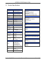
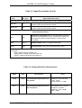
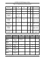
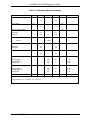
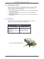
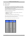
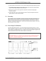
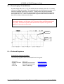
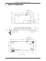
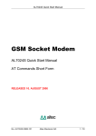
AL7020S, AL7024S Designer’s Guide
GSM Socket Modem
AL7020S, AL7020S-3V Series
AL7024S, AL7024S-3V Series
Designer’s Guide
RELEASED 9. JANUARY 2006
Doc. No. DG_7024E
Altec Electronic AG
Seite 1 / 32
AL7020S, AL7024S Designer’s Guide
Information provided by Altec Electronic AG is believed to be accurate and reliable.
However, no responsibility is assumed by Altec Electronic for its use, nor any
infringement of patents or other rights of third parties which may result from its use.
No license is granted by implication or otherwise under any patent rights of Altec
other than for circuitry embodied in Altec products. Altec Electronic reserves the right
to change circuitry at any time without notice. This document is subject to change
without notice. Please read carefully the safety precautions for a terminal based on
the AL7020S and AL7024S Socket Modems.
Product names or services listed in this publication are for identification purposes
only, and may be trademarks or registered trademarks of their respective companies.
All other marks mentioned herein are the property of their respective owners.
© 2006 Altec Electronic AG
Printed in Switzerland
All Rights Reserved
Doc. No. DG_7024E
Altec Electronic AG
Seite 2 / 32
AL7020S, AL7024S Designer’s Guide
Table of Contents
1.
INTRODUCTION ..........................................................................................................5
1.1 Models Description .......................................................................................................5
1.2 Summary ......................................................................................................................5
1.3 Product Specifications ..................................................................................................6
2.
TECHNICAL OVERVIEW.............................................................................................7
2.1 Block Diagramm of GSM Module .................................................................................7
2.2 Supported Interfaces ....................................................................................................7
3.
HARDWARE INTERFACE ...........................................................................................8
3.1 Interface Signals...........................................................................................................8
3.2 Signal Description.........................................................................................................8
3.4 Antenna Interface (RF) ...............................................................................................15
3.4.1
RF Connector: ....................................................................................................15
3.4.2
Antenna Performance Recommendations..........................................................16
3.4.3
Antenna Installation ............................................................................................16
3.4.4
User Operation ...................................................................................................16
3.5 Internal SIM Card Interface ........................................................................................17
3.5.1
SIM Card reader pins supported:........................................................................17
3.6 SIM Card Mechanical Drawings .................................................................................18
3.7 External SIM Card Interface (-ES Option) ..................................................................19
3.7.1
External SIM Card reader pins supported: .........................................................19
3.7.2
SIM socket pin description:.................................................................................19
3.7.3
SIM Card Reader Integration:.............................................................................20
3.7.4
Layout Restrictions: ............................................................................................20
3.8 Audio - Interface .........................................................................................................21
3.8.1
Speaker-Circuit ...................................................................................................21
3.8.2
Microphone circuit...............................................................................................22
3.8.3
Audio Circuit Design Considerations ..................................................................22
3.9 Reset Signal (ON/OFF Signal) ...................................................................................23
3.9.1
Software Reset ...................................................................................................23
4.
CONNECTORS AND PERIPHERAL REFERENCE...................................................24
4.1
RF CONNECTOR...................................................................................................24
4.2
Microphone.............................................................................................................24
4.3
Speaker ..................................................................................................................24
4.4
Antenna Cable........................................................................................................24
4.5
GSM antenna .........................................................................................................24
5.
DESIGN GUIDELINES ...............................................................................................25
5.1 Electromagnetic Interference (EMI) Considerations ...................................................25
5.1.1
Grounding ...........................................................................................................26
5.1.2
Power Supply 5V (5V Models)............................................................................26
5.1.3
Power Supply 3.3V (3V Models).........................................................................27
5.1.4
Preferred Regulators ..........................................................................................27
5.1.5
RF Antenna.........................................................................................................28
5.2 Manufacturing Considerations....................................................................................28
6.
MODULE DIMENSIONS ............................................................................................29
7.
REGULATORY APPROVALS ....................................................................................30
7.1 Considerations for Regulatory Approvals ...................................................................30
7.1.1
Regulatory Requirements ...................................................................................30
7.1.2
Regulatory Statement .........................................................................................30
7.2 Safety Precautions .....................................................................................................31
7.2.1
User Operation ...................................................................................................31
7.2.2
Antenna Installation ............................................................................................31
7.2.3
Antenna care and replacement...........................................................................31
7.2.4
Electronic devices...............................................................................................31
8.
APPENDIX A ..............................................................................................................32
8.1
REFERENCE DOCUMENTS .................................................................................32
Doc. No. DG_7024E
Altec Electronic AG
Seite 3 / 32
AL7020S, AL7024S Designer’s Guide
List of Tables & Figures
Table 3-1. Serial TTL Signals...................................................................................................9
Table 3-2. Signal Descriptions ...............................................................................................10
Table 3-3. Signal Descriptions (Cont'd)..................................................................................11
Table 3-3. Signal Descriptions (Cont'd)..................................................................................12
Table 3-4. Analog Electrical Characteristics...........................................................................12
Table 3-5. Digital Electrical Characteristics............................................................................13
Table 3-6. Absolute Maximum Ratings ..................................................................................14
Table 3.7 Antenna Performance Recommendations ............................................................16
Table 3.8. Headset Speaker Output at Maximum Volume Level ...........................................21
FIGURE 2-1. INTERFACE BLOCK DIAGRAM ...................................................................................7
FIGURE 3-1. SERIAL PINOUT.......................................................................................................9
FIGURE 3-5. SIM CARD READER ..............................................................................................17
FIGURE 6-2. MECHANICAL DRAWINGS .......................................................................................29
Doc. No. DG_7024E
Altec Electronic AG
Seite 4 / 32
AL7020S, AL7024S Designer’s Guide
1.
INTRODUCTION
1.1
Models Description
Models
Interface Connectors
Interfaces / Power
AL7020S
GSM 900/1800 MHz
• DIL-64 Header (RM2) • RS232 TTL Level
• MMCX RF Connector • 5 VDC Power
AL7020S-3V
GSM 900/1800 MHz
• DIL-64 Header (RM2) • RS232 TTL Level
• MMCX RF Connector • 3.3 VDC Power
AL7020S-ES
GSM 900/1800 MHz
• RS232 TTL Level
• DIL-64 Header (RM2)
• SIM Card Interface
• MMCX RF Connector
• 5 VDC Power
AL7024S
AL7024S-3V
1.2
Operating Bands
GSM
GSM
• DIL-64 Header (RM2) • RS232 TTL Level
850/900
1800/1900 MHz • MMCX RF Connector • 5 VDC Power
• RS232 TTL Level
• DIL-64 Header (RM2)
850/900
• SIM Card Interface
1800/1900 MHz • MMCX RF Connector
• 5 VDC Power
Summary
Altec’s AL7020S, AL7024S Socket Modem provides the OEM with a complete E-GSM/GPRS
900/1800Mhz or GSM 850/1900Mhz dual-band module in a compact socket-mountable
module.
The compact size and high level of integration of the Socket Modem minimizes real estate and
cost for motherboard and box modem applications. Its low power consumption makes it ideal
for portable applications such as pocket modems and for a wide variety of embedded control
applications. The pin compatibility between the full range of all ALXXXX Series Socket
Modems and ISDN Socket TA's allows upgrading and production configurability without
hardware changes.
This designer's guide describes the modem hardware. AT commands and S registers are
defined in the AT Command Reference Manual.
As a data modem in CSD mode, the AL7020S and AL7024S Socket Modem can receive data
at speeds up to 14.4 Kbps and can send data at speeds up to 14.4 Kbps. Error correction
V.42 maximize data transfer integrity. Non-error-correcting mode is also supported.
As a fax modem, the AL7020S Socket Modem supports Group 3 send and receive rates up to
14.4 kbps and supports Class I and T.30 protocols.
The Socket Modem with Voice features supports Full Rate, Enhanced Rate and Half Rate
(FR/EFR/HR). This mode supports applications such as digital telephone answering machine
(TAM), voice annotation, audio recording and playback.
The AL7020S Socket Modems supports GPRS Class B and multislot classes up to Class 8
with coding shemes CS1 to CS4. The AL7024S Socket Modems supports GPRS Class B and
multislot classes up to Class 10 with coding schemes CS1 to CS4
SMS services are supported in both GSM and GPRS modes.
The GSM Socket Modems are available with internal and external SIM Card Readers.
Doc. No. DG_7024E
Altec Electronic AG
Seite 5 / 32
AL7020S, AL7024S Designer’s Guide
1.3
Product Specifications
Voice Functions
Product Features
Operating
systems:
EGSM: 900/1800 MHz
GSM: 850/1900 MHz
Physical Characteristics
Size:
64.5 x 26.5 mm Socket
Modem Form Faktor
Mounting:
Through DIL-64 connectors
Weight:
-20°C +60° C
Functional temp.
-30°C +70° C
Storage temp.
-40°C +85°C
GSM Supplementary Services
USSD Phase II
Call forwarding
Call hold, waiting and multiparty
Call diverting
Missed-call indicator
AOC
Call barring
Environmental
Operational
temp.
Telephony
Digital audio
Differential analog audio lines
Vocoders EFR/ER/FR/AMR
DTMF support
Audio control: echo cancellation, noise
suppression, side tone and gain control
Character Set
Performance
UTF8
UCS2trol/Status Indicators
Operating
Voltage:
3.3V / 5V
Current
consumption :
< 2.5 mA @ DRX9 (Idle
mode
Tx power:
• 0.8 W, 850 MHz
• 2 W, 900 MHz
• 1 W, 1800/1900 MHz
Control / Status Indicators
GPRS coverage
Wakeup
TX enable
Reset
Features over RS232
Interfaces
Connectors:
SIM Card:
Serial RS232:
• DIL-64 Header (RM2)
• RF MMCX
• Local SIM connectivity
• 32K SIM
• 1.8 / 3.0 V
• BR from 300 bps to 115
Kbps
• Auto BR from 300 bps
to 115 Kbps
Data Features
GPRS:
• Multi-slot class 8 / 10
(4 down; 2 up)
• Max BR 85.6 Kbps
• Class B GSM 07.10
multiplexing protocol
• Coding scheme CS1-CS4
CSD:
Max BR 14.4 Kbps
SMS:
• MO/MT Text and PDU
modes
• Cell broadcast
Embedded TCP/IP stack
STK Class II
Emergency and Location
FCC E911 Phase II Location Mandate using
EOTD
AT Command Set
GSM 07.05
GSM 07.07
Motorola proprietary AT commands
Accessories
Developer Kit
Antennas
RF Cables
FAX Class 1
Doc. No. DG_7024E
Altec Electronic AG
Seite 6 / 32
AL7020S, AL7024S Designer’s Guide
2.
TECHNICAL OVERVIEW
2.1
Block Diagramm of GSM Module
2.2
Supported Interfaces
The major hardware signal interfaces of the DF Series SocketGSM Modem are illustrated
in Figure 1-1.
5
TTL
Serial
interface
External SIM
(Optional)
Leds
1
3
3
1
Socket
GSM
Modem
Module
1
1
2
Antenna
Interface
Speaker
Microphone
Interface
Figure 2-1. Interface Block Diagram
•
•
•
•
•
•
The RS232 Interface is connected via eight pins to the module.
The SIM card is connected via 4 pins to the module.
The Microphone is connected via 2 pins to the module.
The Speaker is connected via one pin to the module.
The Indicators are connected via two pins to the module.
The power supply is connected via one pin to the module.
Doc. No. DG_7024E
Altec Electronic AG
Seite 7 / 32
AL7020S, AL7024S Designer’s Guide
3.
HARDWARE INTERFACE
3.1
Interface Signals
The Socket Modem pin assignments with DTE serial TTL interface, SIM Card and Analog
Interface are shown in Figure 3-1 and are listed in Table 3-1.
3.2
Signal Description
The Socket Modem interface signals are described in Table 3-3.
The digital electrical characteristics are listed in Table 3-4.
The analog electrical characteristics are listed in Table 3-5.
Doc. No. DG_7024E
Altec Electronic AG
Seite 8 / 32
AL7020S, AL7024S Designer’s Guide
1
2
NC
NC
SPKR
AGND
MIC
VCC
64
63
62
61
POWER
AUDIO
Top View
24
25
26
27
28
29
30
31
32
SIM / LED
INTERFACE
RESET#
NC
DGND
LED-GPRS
SIMVCC
GSM LED
SIMDATA
SIMRST
SIMCLK
DGND
DTR#
DCD#
CTS#
DSR#
RI#
TXD#
RXD#
RTS#
41
40
39
38
37
36
35
34
33
SERIAL TTL
INTERFACE
Notes: Pins 3-23 and 42-60 are not installed.
Figure 3-1. SERIAL PINOUT
Table 3-1. Serial TTL Signals
PI
N
NAME
I/O TYPE
PIN NAME
I/O TYPE
1
2
3
4
5
6
7
8
9
10
11
12
13
14
15
16
17
18
19
20
21
22
23
24
25
26
27
28
29
30
31
32
NC
NC
No pin
No pin
No pin
No pin
No pin
No pin
No pin
No pin
No pin
No pin
No pin
No pin
No pin
No pin
No pin
No pin
No pin
No pin
No pin
No pin
No pin
~RESET
NC
DGND
LED GPRS
SIMVCC (option)
LED GSM
SIMDATA (option)
SIMRST (option)
SIMCLK (option)
NC
NC
33
34
35
36
37
38
39
40
41
42
43
44
45
46
47
48
49
50
51
52
53
54
55
56
57
58
59
60
61
62
63
64
Input
Output
Input
Output
Output
Output
Output
Input
GND Digital
Doc. No. DG_7024E
Input
NC
GND Digital
Output
Output
Output
Bi-directional
Output
Output
~RTSTTL
~RXDTTL
~TXDTTL
~RITTL
~DSRTTL
~CTSTTL
~DCDTTL
~DTRTTL
DGND
No pin
No pin
No pin
No pin
No pin
No pin
No pin
No pin
No pin
No pin
No pin
No pin
No pin
No pin
No pin
No pin
No pin
No pin
No pin
VCC
MICV
AGND
SPKR
Altec Electronic AG
POWER +5V
Input
GND Analog
Output
Seite 9 / 32
AL7020S, AL7024S Designer’s Guide
Table 3-2. Signal Descriptions
Label
I/O Type
Signal Name/Description
+5 VDC. A standard 5V +/- 5% - 1.5A power supply is strictly required to
supply this module (5V Versions). Average current is 270mA
(350mA @ PCL5). See also chapter 5.1.2
VCC
PWR
+3.-3 VDC. A standard 3.3V +/- 5% - 1A power supply is strictly required to
supply this module (3V Versions). Average current is 270mA
(350mA @ PCL5). See also chapter 5.1.3
GND
GND
Digital Ground Connect to Digital Ground on the interface circuit.
~RESET
IC
Modem Reset (ON/OFF). To be pulled to ground by external transistor for
reset. (on module pull-up resistor of 200K). The GSM Modem has already an
internal power-up reset circuit. Needs special timing for RESET and ON/OFF
function (see chapter 3.8)
AGND
GND
Analog Ground. if a microphone or headset is used, use this as a ground. If
these are never used, it can be connected to DGND.
OPTIONAL SIM CARD READER INTERFACE
Label
I/O Type
Signal Name/Description
SIMCLK
O
SIM Clock. Provided from module.
SIMRST
O
SIM Reset. Provided from Module to reset the SIM Card.
SIMDATA
I/O
SIM Data line. Digital, bi-directional data line to exchange data between
module and SIM card.
SIMVCC
PWR
SIM Power Supply. 3VDC Power Supply provided from module to power
the SIM Card. Only 3V SIM Cards are supported.
Doc. No. DG_7024E
Altec Electronic AG
Seite 10 / 32
AL7020S, AL7024S Designer’s Guide
Table 3-3. Signal Descriptions (Cont'd)
Label
I/O Type
Signal Name/Description
The Serial interface signals are TTL-level signals.
~RTSTTL
IB
~RXDTTL
OB
~TXDTTL
IA
Request To Send (TTL Active Low). ~RTS is used to condition the local
modem for data transmission and, during half-duplex operation, to control
the direction of data transmission.
On a full-duplex channel, RTS OFF maintains the modem in a non-transmit
mode. A non-transmit mode does not imply that all GSM signals have been
removed from the link. RTS OFF may be ignored if the modem is optioned to
strap ~CTS ON; this allows the modem to receive from the DTE even though
RTS is OFF.
RTS input ON causes the modem to transmit data on TXD when ~CTS
becomes active.
Received Data (TTL Active Low). The modem uses the ~RXD line to send
data received from the telephone line to the DTE and to send modem
responses to the DTE. Modem responses take priority over incoming data
when the two signals are in competition for ~RXD.
Transmitted Data (TTL Active Low). The DTE uses the ~TXD line to send
data to the modem for transmission over the telephone line or to transmit
commands to the modem. The DTE should hold this circuit in the mark state
when no data is being transmitted or during intervals between characters.
~CTSTTL
OB
Clear To Send (TTL Active Low). ~CTS is controlled by the modem to
indicate whether or not the modem is ready to transmit data. ~CTS ON,
together with the ~RTS ON, ~DSR ON, and ~DTR ON (where implemented),
indicates to the DTE that signals presented on TXD will be transmitted.
~CTS OFF indicates to the DTE that it should not transfer data across the
interface on TXD. ~CTS ON is a response to ~DTR ON and ~RTS, delayed
as may be appropriate for the modem to establish a connection.
~RITTL
OB
Ring Indicate (TTL Active Low). ~RI output ON (low) indicates the
presence of an incoming call.
~DSRTTL
OB
Data Set Ready (TTL Active Low). ~DSR indicates modem status to the
DTE. ~DSR OFF (high) indicates that the DTE is to disregard all signals
appearing on the interchange circuits except Ring Indicator (~RI).
~DCDTTL
OB
Data Carrier Detect (TTL Active Low). When AT&C0 command is not in
effect, ~DCD output is ON when a link is established or OFF when no link is
established.
IA
Data Terminal Ready (TTL Active Low). The ~DTR input is turned ON
(low) by the DTE when the DTE is ready to transmit or receive data. ~DTR
ON prepares the modem to be connected and maintains the connection
established by the DTE (manual answering) or internally (automatic
answering). ~DTR OFF places the modem in the disconnect state under
control of the &Dn command. The effect of ~DTR ON and ~DTR OFF
depends on the &Dn command.
~DTRTTL
Doc. No. DG_7024E
Altec Electronic AG
Seite 11 / 32
AL7020S, AL7024S Designer’s Guide
Table 3-3. Signal Descriptions (Cont'd)
Label
I/O Type
Signal Name/Description
LED driver lines are open-drain inverter-driven (74HCT05) lines with 1.5 KΩ, 1/10W pull-up resistors.
GSM LED
OG
GSM activity LED. active low !
connect LED to 5V with resistor in series.
GPRS LED
OG
GPRS activity LED. active low !
connect LED to 5V with resistor in series.
Audio/Headset Interface
MICV
I(DA)
Microphone Voice Input. MICV is a single-ended microphone
input from the analog switch circuit. The maximum input to the
MICV pin before there is signal distortion in the network is
12mVRMS.
SPKR
O(DF)
Speaker Output. SPKR is a single-ended output.
AGND
PWR
Analog Ground. Analog Ground related to MICV Input.
Notes:
1. I/O types:
I(DA) = Analog input (see Table 3-5).
O(DD),O(DF) = Analog output (see Table 3-5).
IO(DX) = Analog input/output (see Table 3-5).
Table 3-4. Analog Electrical Characteristics
Name
Type
SPKR
O(DF)
Recommended characteristics for
the speaker:
Impedance: 32 Ω (handset)
Power: 10mW
Sound Pressure.: 110dB
MICV
I(DA)
Recommended characteristics for
the microphone:
Bias Voltage: 2.2V ( 0.5mA )
Impedance: 2 KOhms
Sensitivity: –40 to –50dB
SNR: > 50dB
Doc. No. DG_7024E
Characteristic
Altec Electronic AG
Value
Seite 12 / 32
AL7020S, AL7024S Designer’s Guide
Table 3-5. Digital Electrical Characteristics
Parameter
Symbol
Min.
Typ.
Max.
Input High Voltage
pins 33,35,40
VIH
2
-
5.5
Vdc
Input Low Voltage
pins 33,35,40
VIL
0
-
0.8
Vdc
Output High
Voltage
pins 34,36,37,38
VOH
VCC-0.1V
VCC
-
Vdc
3.8V
@VCC=4.5V
4.2
-
ILOAD = -4 mA
Output High
Voltage
VCC=4.5V
pin 39
VOH
VCC-0.1
VCC
-
ILOAD= -50 uA
3.8V
-
-
ILOAD = -8 mA
Output Low
Voltage
pins 34,36,37,38
VOL
-
0
0
0.1
0.33
Output Low
Voltage
VCC=4.5V
pin 39
VOL
-
-
0.1
0.44
-
-
0.8
max Reset Low
Input Voltage
pin 24
Parameter
VIL
ILOAD= -20 uA
Vdc
ILOAD = 20 uA
ILOAD = 4.8 mA
Vdc
Conditions
Min
0.7xSIMVCC
SIMRST
SIMDATA
SIMCLK
VOH
IIH = ± 20µA
IIL = 1 mA
Source
current
= 20µA
SIMRST
SIMDATA
SIMCLK
VOL
Sink current
= -200µA
SIMVCC*
Output Voltage
SIMCLK
Rise / Fall Time
ISIMVCC < =
6mA
Loaded with
30pF
SIMRST
SIMDATA
Rise / Fall Time
SIMCLK
Frequency
SIMDATA VIH
SIMDATA VIL
Units Test Conditions
Typ
ILOAD = 50 uA
ILOAD = 8 mA
internally pulled
up to VCC by
10kΩ
Max
Unit
0.3xSIMVCC
V
V
SIMVCC –
0.1V
V
0.1
V
2.85
V
50
ns
Loaded with
30pF
1
µs
Loaded with
30pF
3.25
MHz
Doc. No. DG_7024E
2.70
Altec Electronic AG
2.80
Seite 13 / 32
AL7020S, AL7024S Designer’s Guide
Table 3-6. Absolute Maximum Ratings
Parameter
Supply Voltage
Symbol
Min.
Static Discharge Voltage
Vdc
Storage Temperature Range
-
5.25
3.45
V
-
+/- 2500
TA
°C
-20
-20
-
+60
+70
TSTG
°C
-
+85
ID
mA
Average @PCL5
Average @PCL10
Average Idle
Supply Current GSM 1800
+7.0
VESD
-40
Supply Current GSM 900
-
Vdc
4.75
3.20
Operational
Functional
Test Condition
+6.0
VDD
@ 25°C
Operating Temperature Range
-
VIN
5V Version
3V Version
Units
Vdc
-0.5
Nominal Supply Voltage
Max.
VDD
-0.3
Input Voltage
Typ.
280
170
30
360
@ 3.3V
@ 3.3V
@ 3.3V
45
ID
mA
Average @PCL5
Average @PCL10
Average Idle
230
170
30
310
45
@ 3.3V
@ 3.3V
@ 3.3V
Notes:
Test Conditions: VCC = 5VDC +/- 5%, TA = 25°C,
Doc. No. DG_7024E
Altec Electronic AG
Seite 14 / 32
AL7020S, AL7024S Designer’s Guide
3.4
Antenna Interface (RF)
The AL7020S has two models, one for North America Frequency bands (850/1900
MHz), and one for European Bands (900/1800 MHz). The following connection
requirements apply for the AL7020S antenna:
• The AL7020S is terminated with an MMCX connector, and with 50-ohm impedance
in the relevant frequencies.
• The AL7020S can be connected to any antenna with 50-ohm impedance in the
relevant frequency bands.
• The AL7020S is designed to work on VSWR, up to 3:1 The antenna should meet
this requirement.
3.4.1 RF Connector:
The Antenna-jack of the AL7020S module is an MMCX type. It has a snap-in
connection. For the antenna-cable RG178 is recommended.
RF Connector
AL7020S Connector
Mating Connector
Standard MMCX female
Amphenol:
Standard MMCX male
MMCX 6251S5-3GT30G-50 (connector for cable)
gold plated
FIGURE 3-4. Antenna Connector Interface
Doc. No. DG_7024E
Altec Electronic AG
Seite 15 / 32
AL7020S, AL7024S Designer’s Guide
3.4.2 Antenna Performance Recommendations
Table 3.7 - Antenna Performance Recommendations
GSM 850
GSM 900
DCS 1800
PCS 1900
Gain:
Impedance:
VSWR:
Frequencies:
TX 824 – 849 MHz
RX 869 – 893 MHz
TX 880 – 915 MHz
RX 925 – 960 MHz
TX 1710 – 1785 MHz
RX 1805 – 1880 MHz
TX 1850 - 1910 MHz
RX 1930 – 1990 MHz
0 dBi (unity) gain or
greater
50 Ohm
Typical: 1.5:1
Worst case: 2.5:1
3.4.3 Antenna Installation
• A minimum separation distance of 20 cm needs to be maintained between the
antenna and all persons.
• The transmitter effective radiated power must be less than 3.0 Watts ERP (4.9
Watts or 36.9 dBm EIRP). This requires that the combination of antenna gain and
feed line loss does not exceed 16 dBi.
3.4.4 User Operation
Do not operate your unit when a person is within 8 inches (20 centimeters) of the
antenna. A person or object within 8 inches (20 centimeters) of the antenna could
impair call quality and may cause the phone to operate at a higher power level than
necessary.
IMPORTANT: The unit must be installed in a manner that provides a minimum
separation distance of 20 cm or more between the antenna and persons to satisfy
FCC RF exposure requirements for mobile transmitting devices.
IMPORTANT: To comply with the FCC RF exposure limits and satisfy the categorical
exclusion requirements for mobile transmitters, the following requirements must be
met:
Doc. No. DG_7024E
Altec Electronic AG
Seite 16 / 32
AL7020S, AL7024S Designer’s Guide
3.5
Internal SIM Card Interface
The AL7020S module has a built-in SIM card reader within the module itself (see
figure 3.5). The SIM card is inserted into the slot provided on the side of the
connectors (bottom side).
The SIM Interface controls a 3V SIM card. This interface is fully compliant with GSM
11.11 recommendation concerning SIM functions.
3.5.1 SIM Card reader pins supported:
Signal
Pin No
I/O
Description
SIMVCC
1
O
SIM Power Supply
SIMRST
2
O
SIM Reset
SIMCLK
3
O
SIM Clock
SIMGND
5
O
SIM GND
SIMDATA
7
I/O
SIM Data
SIMPRES
8
I
SIM Card Detect not
supported
SIM Card
Reader
Bottom
View
Figure 3-5. SIM CARD READER
Doc. No. DG_7024E
Altec Electronic AG
Seite 17 / 32
AL7020S, AL7024S Designer’s Guide
3.6
SIM Card Mechanical Drawings
Doc. No. DG_7024E
Altec Electronic AG
Seite 18 / 32
AL7020S, AL7024S Designer’s Guide
3.7
External SIM Card Interface (-ES Option)
4 signals exist:
• SIMVCC: SIM power supply.
• SIMRST: reset.
• SIMCLK: clock.
• SIMDATA : I/O port.
The SIM interface controls a 3V SIM. This interface is fully compliant with GSM 11.11
recommendations concerning SIM functions. It is recommended to add Transient
Voltage Suppressor diodes on the signal connected to the SIM socket in order to
prevent any Electrostatic Discharge. TVS diodes with low capacitance (less than
10pF) have to be connected on SIMCLK and SIMDATA to avoid any disturbance of
the rising and falling edge. These types of diodes are mandatory for the Full Type
Approval. They shall be placed as close as possible to the SIM socket.
3.7.1 External SIM Card reader pins supported:
Signal
Pin number
I/O
I/O type
Description
SIMCLK
32
O
2X
SIM Clock
SIMRST
31
O
2X
SIM Reset
SIMDATA
30
I/O
CMOS / 3X
SIM DATA
SIMVCC
28
O
SIM Power Supply
3.7.2 SIM socket pin description:
Signal
Pin Number
VCC
RST
CLK
CC4
GND
VPP
I/O
CC8
1
2
3
4
5
6
7
8
Description
SIMVCC
SIMRST
SIMCLK
VCC module (Not connected)
GROUND
Not connected
SIMDATA
SIMPRES (Not connected)
TOP VIEW
GND
SIMDATA
Doc. No. DG_7024E
5
1
6
2
7
3
8
4
Altec Electronic AG
SIMVCC
SIMRST
SIMCLK
Seite 19 / 32
AL7020S, AL7024S Designer’s Guide
3.7.3 SIM Card Reader Integration:
SIM interface controls a 3V SIM only.
We add Transient Voltage Suppressor (TVS) diodes with low capacitance (less than
10pF) on signal connected to the SIM socket in order to prevent any Electrostatic
Discharge. They shall be placed as close as possible to the SIM socket. Following
references are used:
DALC208SC6 from ST Microelectronics, which will be connected, to SIMCLK and
SIMDATA.
ESDA6V1 from ST Microelectronics for the ESD protection of SIMVCC.
On the board near SIM connector, we also add on SIMVCC a 100nF capacitor in
parallel as close as possible to the SIM connector to minimize noise.
Schematic of SIM Interface:
P1A
PRES_OUT
PRES_IN
I/O
VPP
GND
CLK
SIM-CARD-READER
RST
VCC
8
4
7
6
5
3
2
1
32
31
30
29
28
27
26
25
24
SIMDATA
SIMCLK
SIMRST
SIMVCC
P1
SOCKET MODEM
C1
100NF
3
2
1
5
6
3
DALC208SC6
D1
ESDA6V1L
D2
4
1
2
RESET
3.7.4 Layout Restrictions:
For the SIM interface, length of the tracks between the GSM modem and the SIM
connector should be as short as possible (8cm).
EMI layout is recommended for SIMCLK signal.
SIMCLK
GND
GND
SIM
connector
SIMRST
SIMVCC
SIMDATA
GND
Socket
Modem
Less than 8 cm
Doc. No. DG_7024E
Altec Electronic AG
Seite 20 / 32
AL7020S, AL7024S Designer’s Guide
3.8
Audio - Interface
3.8.1 Speaker-Circuit
Audio output is useful for monitoring the modem's call-progress tones and modem
system debugging, as well as for fullfeatured Voice applications. You can directly
connect a speaker of 32 to 150 Ohms to pins 63 and 64. The connection is singleended, with analog-ground at pin 63. Use good shielding of the audio-connections as
to avoid disturbing performance by entering RF.
The gain of the SPK output is internally adjusted and can be tuned using an AT
command. The possible range of output-levels is 4mV to 210mV rms (max. Levels).
Recommended characteristics for the speaker:
• Type: 10mW, electro-magnetic
• Impedance: 32 to 150 Ohms / 1nF (32Ohm for headsets, 150Ohms other
applications)
• Sensitivity (SPL): 100dB min
• Frequency response compatible with the GSM specifications
Table 3.8 shows the Speaker output in headset mode for different network signal
levels when the g20 is set to the maximum volume level.
Table 3.8. Headset Speaker Output at Maximum Volume Level
dBm0 mV RMS
dBm0
mV RMS
Headset
Speaker
(mV RMS)
3.14
1111.9
174
0
774.6
165
-5
435.6
132
-10
244.9
72
-15.5
130
39
-16
122.8
36
-17
109.4
32
-20
77.5
24
-25
43.6
5
-30
24.5
4
max
3000
210
Speak
Doc. No. DG_7024E
Altec Electronic AG
Seite 21 / 32
AL7020S, AL7024S Designer’s Guide
3.8.2 Microphone circuit
The AL7020S has an analog input, referenced to the microphone ground (pin 63).
The AL7020S contains an analog amplifier with a default gain of 22dB, which can be
adjusted in seven steps between 0 and 31dB using the AT+MMICG command. For
more details about this command, refer to the AT Commands document (AT_7020A).
When the default gain of 22dB is used, then the level considerations should be as
follows:
Pin 62 is the headset microphone input. The input for this line can come directly from
a headset microphone. The maximum input to the AL7020S headset microphone
before there is signal distortion in the network is 12 mvRMS.
The Microphone ist connected single-ended to pin 62, with analog ground at pin 63.
At pin 62 there is also a phantom feeding-voltage of 2.2 Volts.
Recommended characteristics for the microphone:
•
•
•
•
•
2V – 0.5mA
KOhms
Sensitivity -40 to –50dB
SNR > 50dB
Frequency response compatible with the GSM specifications
3.8.3 Audio Circuit Design Considerations
In order to design an audio circuit that produces clear audio, without being affected by
the GSM transmission, the following guidelines should be considered when designing
the circuit:
•
•
•
•
•
•
•
The audio input to the AL7020S should be referenced to the MIC GND line of the
Module.
The microphone bias of the AL7020S for the microphone is 2.2 V. If a microphone
with a different voltage is used, the bias should be as clean as possible, and
referenced to MIC GND. Because most GSM buzz (217Hz TDMA noise) is
generated from the microphone path, if a different bias is created, it should be
filtered to supply DC only.
The MIC GND and GND are connected inside the module and should not be
connected to the application board.
Keep the lines of the microphone inputs as short as possible. To filter the lines
from RF emission, 39pF capacitors can be used.
The Module GND should be connected on all pins.
If possible, the RF cable ground from the AL7020S should be connected to the
GND of the Module.
The digital lines of the application should never be referenced to the MIC
GND(63).
Doc. No. DG_7024E
Altec Electronic AG
Seite 22 / 32
AL7020S, AL7024S Designer’s Guide
3.9
Reset Signal (ON/OFF Signal)
After power is applied to the AL7020S module, the power-on process is initiated,
which lasts about five seconds, after which the module is ready to communicate. After
power-on, the on/off signal is pulled high to the VCC by a 200kΩ resistor. The module
remains active until power is turned off or the power-off process is initiated by
activating the Reset (ON/OFF) signal. The AT interface answers "OK" to the
application, when the reset is complete.
After the AL7020S is turned on, the line should be pulled low for a minimum of 2
seconds to turn it off. The unit can be turned off only if at least 10 seconds have
elapsed since turning it on. To turn the AL7020S on again, the on/off signal should be
pulled low for a minimum of 800 ms.
Figure 3.8 shows the timing diagram for the on/off signal.
Figure 3.8. On/Off Signal Timing Diagram
T1
T2
T3
In Figure 3.8, the following timing requirements apply:
• T1 minimum = 800 ms.
• T2 minimum = 10 seconds.
• T3 minimum = 2 seconds.
3.9.1 Software Reset
It is possible to reset the module by software, which activates an internal reset
generator (see AT Commands Reference Manual).
Doc. No. DG_7024E
Altec Electronic AG
Seite 23 / 32
AL7020S, AL7024S Designer’s Guide
4.
CONNECTORS AND PERIPHERAL REFERENCE
4.1
RF CONNECTOR
RF MMCX-connector and accessories can be obtained from
• RADIALL (http://www.radiall.com/)
• AMPHENOL (http://www.amphenol.com/)
• HUBER&SUHNER (http://www.hubersuhner.com/)
4.2
Microphone
Possible references :
• HOSIDEN KUF3323
• HOSIDEN KUF4323
• PANASONIC WM64
4.3
Speaker
Possible references :
• SANYO M15X0080
• PHILIPS
• PRIMO
4.4
Antenna Cable
The following cable reference has been qualified for being mounted on the AL7020S module.
• RG178
4.5
GSM antenna
GSM antennas and support for antenna adaptation can be obtained from manufacturers such
as:
• ALLGON (http://www.allgon.com )
• MOTECO (http://www.moteco.com )
• AMPHENOL (http://www.amphenol.com )
• GALTRONICS (http://www.galtronics.com )
• RADIALL / LARSEN (http://www.larsenantennas.com/)
• RANGESTAR (http://www.rangestar.com/)
Doc. No. DG_7024E
Altec Electronic AG
Seite 24 / 32
AL7020S, AL7024S Designer’s Guide
5.
DESIGN GUIDELINES
Good engineering practices must be adhered to when designing a printed circuit
board (PCB) containing the GSM Socket Modem module. Suppression of noise is
essential to the proper operation and performance of the modem itself and for
surrounding equipment.
Two aspects of noise in an OEM board design containing the GSM Socket Modem
module must be considered: on-board/off-board generated noise that can affect
analog signal levels and analog-to-digital conversion (ADC)/digital-to-analog
conversion (DAC), and on-board generated noise that can radiate off-board. Both onboard and off-board generated noise that is coupled on-board can affect interfacing
signal levels and quality, especially in low level analog signals. Of particular concern
is noise in frequency ranges affecting modem performance.
On-board generated electromagnetic interference (EMI) noise that can be radiated or
conducted off-board is a separate, but equally important, concern. This noise can
affect the operation of surrounding equipment. Most local governing agencies have
stringent certification requirements that must be met for use in specific environments.
Proper PC board layout (component placement, signal routing, trace thickness and
geometry, etc.), component selection (composition, value, and tolerance), interface
connections, and shielding are required for the board design to achieve desired
modem performance and to attain EMI certification.
5.1
Electromagnetic Interference (EMI) Considerations
The EMC tests have to be performed as soon as possible on the application to
detect any possible problem. When designing, special attention should be paid to:
• Possible spurious emission radiated by the application to the RF receiver in the
receiver band.
• Metallic case or plastic casing with conductive paint are recommended
The following guidelines are offered to specifically help minimize EMI generation.
Some of these guidelines are the same as, or similar to, the general guidelines but
are mentioned again to reinforce their importance. In order to minimize the
contribution of the Socket Modem-based design to EMI, the designer must
understand the major sources of EMI and how to reduce them to acceptable levels.
1. Keep traces carrying high frequency signals as short as possible.
2. Provide a good ground plane or grid. In some cases, a multilayer board may be
required with full layers for ground and power distribution.
3. Decouple power from ground with decoupling capacitors as close to the Socket
Modem module power pins as possible.
4. Eliminate ground loops, which are unexpected current return paths to the power
source and ground.
5. Locate high frequency circuits in a separate area to minimize capacitive coupling
to other circuits. Distribute high frequency signals continuously on a single trace
rather than several traces radiating from one point.
Doc. No. DG_7024E
Altec Electronic AG
Seite 25 / 32
AL7020S, AL7024S Designer’s Guide
6. Locate cables and connectors so as to avoid coupling from high frequency circuits.
7. If a mulilayer board design is used, make no cuts in the ground or power planes
and be sure the ground plane covers all traces.
8. Minimize the number of through-hole connections on traces carrying high
frequency signals.
9. Avoid right angle turns on high frequency traces. Forty-five degree corners are
good, however, radius turns are better
5.1.1 Grounding
Pins 26 and 41 are for grounding. Connect all of them to the same ground-layer or a
big ground-area on your board. The ground-area should completely cover the area
below and around the module and the regulator. Make the connections as wide as
possible. For better RF-perfomance, connect the metal-housing to ground, very near
the ground-pins of the module.
5.1.2 Power Supply 5V (5V Models)
A power supply with 5.0V DC +/- 5% (5V models) and a minimum power of 1.5A is
strictly required to supply this module. The supply-regulator should be placed as close
to the module as possible (about 5cm or nearer). The 5V-trace between regulator and
module should be at least 2.5mm wide or better an entire layer.
Important:
The module draws up to 1.3A max. for 577µs every 4,6ms at GSM transmit level
PCL5 (2W). Therefore a regulator with fast transient response and good load
regulation is strongly recommended.
Peak 1.3 A
Current
Measurement
@ PCL 5
Doc. No. DG_7024E
Altec Electronic AG
Seite 26 / 32
AL7020S, AL7024S Designer’s Guide
5.1.3 Power Supply 3.3V (3V Models)
A power supply with 3.3V +/- 5% (3V models) and a minimum power of 1A is strictly
required to supply this module. The supply-regulator should be placed as close to the
module as possible (about 5cm or nearer). To keep a short and low impedance
connection between the regulator and the module is very important when supplying
the module with 3.3V. The 3.3V-trace between regulator and module should be at
least 2.5mm wide or better an entire layer.
Important:
The module draws up to 0.8A max. for 577µs every 4,6ms at GSM transmit level
PCL5 (2W). Therefore a regulator with fast transient response and good load
regulation is strongly recommended.
Peak 0.8 A
Current
Measurement
@ PCL 5
5.1.4 Preferred Regulators
Preferred fast response regulators:
The following regulators where tested and found to be good.
- MIC29150
- LP3852 / LP3855
- LM3940
- LTC1778
Doc. No. DG_7024E
Micrel Inc.
National Semiconductor
National Semiconductor
Linear Technology
Altec Electronic AG
www.micrel.com
www.national.com
www.national.com
www.linear.com
Seite 27 / 32
AL7020S, AL7024S Designer’s Guide
5.1.5 RF Antenna
Antenna sub-system and integration in the application is a major issue.
Attention should be paid to :
• Choice of the antenna cable (type, length, performance, thermal resistance, etc)
• Antenna connector (type + losses). These elements could affect GSM
performances such as sensitivity and emitted power
• The antenna should be isolated as much as possible from the digital circuitry
(including the interface signals)
• It is strongly recommended to shield the terminal.
• On terminals including the antenna, a poor shielding could dramatically affect the
sensitivity of the terminal. Moreover, the power emitted through the antenna could
affect the application.
Warning:
Altec Electronic strongly recommends to work with an antenna manufacturer either
to develop an antenna adapted to the application or to adapt an existing
solution to the application. The antenna adaptation (mechanical and electrical
adaptation) is one of the key issues in the design of a GSM terminal.
The antenna-cable and the antenna should be as far as possible away from other
circuitry, specially switching-regulators, analog- and uC digital circuits. It is
recommended to place the antenna-jack near a metal enclosure and go through this
one with the antenna-cable.
5.2
Manufacturing Considerations
The Socket Modem has been designed to be mounted onto the host board in one of
two ways.
The first method consists of soldering two 32-pin strip sockets to the host board and
inserting the Socket Modem into the sockets. A suggested part number for the 32-pin
socket is Sam Tec SMM-132-01-F-S.
The second way is to solder the Socket Modem directly to the host board. The most
efficient way to do this is through a wave solder process. The recommended hole size
for the Socket Modem pins is 0.036 in. ±0.003 in. in diameter. Spacers can be used to
hold the Socket Modem vertically in place during the wave solder process. A spacer
should be placed on pin 32 and pin 64 of the Socket Modem. A suggested part
number for the spacer is BIVAR 938-0.130 for P1(0.310in) option Socket Modems.
The spacers can be left on permanently and will not effect operation.
Socket Modems can be put through a water wash process.
Doc. No. DG_7024E
Altec Electronic AG
Seite 28 / 32
AL7020S, AL7024S Designer’s Guide
6.
MODULE DIMENSIONS
Top View
7.0 mm
Top View
Pin 1
2.0
FIGURE 6-2. MECHANICAL DRAWINGS
Dimensions in Millimeters
Doc. No. DG_7024E
Altec Electronic AG
Seite 29 / 32
AL7020S, AL7024S Designer’s Guide
7.
REGULATORY APPROVALS
The GSM Socket Modem is approved as a host-independent modem module. To
maintain type approvals, permits and/or licenses valid, the guidelines described in this
document must be followed.
7.1
Considerations for Regulatory Approvals
The AL7020S Socket Modem has been assessed and has been found to comply with
the following regulatory approvals:
-
FCC
DOC
PTCRB
R&TTE
EMC
GCF
7.1.1 Regulatory Requirements
The Federal Communications Commission (FEC) requires application for certification
of digital devices in accordance with CFR Title 47, Part 2 and Part 15. This includes
Electromagnetic Energy Exposure (EME) testing. As the AL7020S modem is not a
standalone transceiver but is an integrated module, the AL7020S cannot be tested by
itself for EME certification. It is, however, the integrator’s responsibility to have the
completed device tested for EME certification.
7.1.2 Regulatory Statement
The following safety precautions must be observed during all phases of the operation,
usage, service or repair of any cellular terminal or mobile incorporating the AL7020S
module. Manufacturers of the cellular terminal are advised to convey the following
safety information to users and operating personnel, and to incorporate these
guidelines into all manuals supplied with the product.
Failure to comply with these precautions violates safety standards of design,
manufacture and intended use of the product. Altec assumes no liability for customer
failure to comply with these precautions.
1. The AL7020S must be operated at the voltages described in the technical
documentation.
2. The AL7020S must not be mechanically nor electrically changed. Use of
connectors should follow the guidance of the technical documentation.
3. The AL7020S is designed the meet the EMC requirements of ETS 300 342.
4. When integrating the AL7020S into a system, Altec recommends testing the
system to ETS300342-1.
4. The AL7020S meets the safety requirements of EN60950.
5. Systems using the AL7020S are subject to mandatory EMC testing under directive
89/336/EEC (see item 3 above). Other directives, such as the LVD directive
73/23/EE, may also apply to a system using the AL7020S module.
Doc. No. DG_7024E
Altec Electronic AG
Seite 30 / 32
AL7020S, AL7024S Designer’s Guide
7.2
Safety Precautions
Your GSM terminal is based on the GSM standard for cellular technology. The
GSM standard is spread all over the world. It covers Europe, Asia and some parts
of America and Africa. This is the most used telecommunication standard.
Your GSM terminal is actually a low power radio transmitter and receiver. It
sends out and receives radio frequency energy. When you use your GSM
application, the cellular system which handles your calls controls both the radio
frequency and the power level of your cellular modem.
7.2.1 User Operation
Do not operate your unit when a person is within 8 inches (20 centimeters) of the
antenna. A person or object within 8 inches (20 centimeters) of the antenna could
impair call quality and may cause the phone to operate at a higher power level than
necessary.
IMPORTANT: The unit must be installed in a manner that provides a minimum
separation distance of 20 cm or more between the antenna and persons to satisfy
FCC RF exposure requirements for mobile transmitting devices.
IMPORTANT: To comply with the FCC RF exposure limits and satisfy the categorical
exclusion requirements for mobile transmitters, the following requirements must be
met:
7.2.2 Antenna Installation
A minimum separation distance of 20 cm needs to be maintained between the
antenna and all persons.
The transmitter effective radiated power must be less than 3.0 Watts ERP (4.9 Watts
or 36.9 dBm EIRP). This requires that the combination of antenna gain and feed line
loss does not exceed 16 dBi.
7.2.3 Antenna care and replacement
Do not use the GSM terminal with a damaged antenna. If a damaged antenna
comes into contact with the skin, a minor burn may result. Replace a damaged
antenna immediately. Consult your manual to see if you may change the antenna
yourself. If so, use only a manufacturer-approved antenna. Otherwise, have your
antenna repaired by a qualified technician. Use only the supplied or approved
antenna. Unauthorized antennas, modifications or attachments could damage the
terminal and may contravene local RF emission regulations or invalidate type
approval.
7.2.4 Electronic devices
Most electronic equipment, for example in hospitals and motor vehicles is
shielded from RF energy. However RF energy may affect some improperly
shielded electronic equipment.
Doc. No. DG_7024E
Altec Electronic AG
Seite 31 / 32
AL7020S, AL7024S Designer’s Guide
8.
APPENDIX A
8.1
REFERENCE DOCUMENTS
GSM ETSI recommendations for Phase I and Phase II.
Specification Reference
Title
GSM900/1800/1900 ph2 Radio
ETSI GSM 05.05 v7.1.0 release 1998
GSM ph2 LinkManagement
ETSI GSM 03.06, 04.08, 05.05, 05.08, 05.10,
07.01
and GT 01 v4.2.1
GSM ph2 Layer 2
ETSI GSM 04.06 and GT 01 v4.2.1
GSM900 ph2 Layer 3
ETSI GSM 04.08 and GT 01 v4.2.1
GSM1800 ph2 Layer 3
ETSI GSM 04.08 and GT 01 v4.2.1
GSM900/GSM1800 Multiband
ETSI GSM 02.07, 03.22, 04.08, 04.13, 05.05,
05.08
and GT 01 v4.2.1
GSM ph2 SIM
ETSI GSM 11.11 and GT 01 v4.2.1
GSM ph2 Teleservices
ETSI GSM 03.50 and GT 01 v4.2.1
GSM ph2 Miscellaneous
ETSI GSM 02.07, 03.40, 03.41, 04.08, 04.10,
04.11,
06.10, 06.11, 06.12, 06.31, 06.32, 07.01, 09.07
and
GT 01 v4.2.1
GSM1800 ph2 Miscellaneous
ETSI GSM 02.07, 03.40, 03.41, 04.08, 04.10,
04.11,
06.10, 06.11, 06.12, 06.31, 06.32, 07.01, 09.07
and
GT 01 v4.2.1
GSM1900 ph2+
EN 300 919 V7.1.0 (1999-07) European
standard
(Telecommunications series) Digital cellular
telecommunications system (phase2+)
Doc. No. DG_7024E
Altec Electronic AG
Seite 32 / 32