1
Service Guide
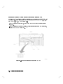
Agilent Technologies
8752C
Network Analyzer
Manufacturing Part Number: 08752-90136
Printed in USA
Print Date: February 1998
Supersedes: December 1997
© Agilent Technologies, Inc. 1998
Hewlett-Packard to Agilent Technologies Transition
This manual may contain references to HP or Hewlett-Packard. Please note that
Hewlett-Packard's former test and measurement, semiconductor products and chemical analysis
businesses are now part of Agilent Technologies. To reduce potential confusion, the only
change to product numbers and names has been in the company name prefix: where a product
number/name was HP XXXX the current name/number is now Agilent XXXX. For example,
model number HP 8752C is now model number Agilent 8752C.
Documentation Warranty
THE MATERIAL CONTAINED IN THIS DOCUMENT IS PROVIDED "AS IS," AND IS
SUBJECT TO BEING CHANGED, WITHOUT NOTICE, IN FUTURE EDITIONS. FURTHER, TO THE MAXIMUM EXTENT PERMITTED BY APPLICABLE LAW, AGILENT
DISCLAIMS ALL WARRANTIES, EITHER EXPRESS OR IMPLIED WITH REGARD TO
THIS MANUAL AND ANY INFORMATION CONTAINED HEREIN, INCLUDING BUT
NOT LIMITED TO THE IMPLIED WARRANTIES OF MERCHANTABILITY AND FITNESS FOR A PARTICULAR PURPOSE. AGILENT SHALL NOT BE LIABLE FOR
ERRORS OR FOR INCIDENTAL OR CONSEQUENTIAL DAMAGES IN CONNECTION
WITH THE FURNISHING, USE, OR PERFORMANCE OF THIS DOCUMENT OR ANY
INFORMATION CONTAINED HEREIN. SHOULD AGILENT AND THE USER HAVE A
SEPARATE WRITTEN AGREEMENT WITH WARRANTY TERMS COVERING THE
MATERIAL IN THIS DOCUMENT THAT CONFLICT WITH THESE TERMS, THE WARRANTY TERMS IN THE SEPARATE AGREEMENT WILL CONTROL.
DFARS/Restricted Rights Notice
If software is for use in the performance of a U.S. Government prime contract or
subcontract, Software is delivered and licensed as “Commercial computer software” as
defined in DFAR 252.227-7014 (June 1995), or as a “commercial item” as defined in FAR
2.101(a) or as “Restricted computer software” as defined in FAR 52.227-19 (June 1987) or
any equivalent agency regulation or contract clause. Use, duplication or disclosure of
Software is subject to Agilent Technologies’ standard commercial license terms, and
non-DOD Departments and Agencies of the U.S. Government will receive no greater than
Restricted Rights as defined in FAR 52.227-19(c)(1-2) (June 1987). U.S. Government users
will receive no greater than Limited Rights as defined in FAR 52.227-14 (June 1987) or
DFAR 252.227-7015 (b)(2) (November 1995), as applicable in any technical data.
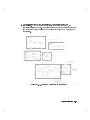
Printing Copies of Documentation from the Web
To print copies of documentation from the Web, download the PDF file from the Agilent
web site:
• Go to http://www.agilent.com.
• Enter the document’s part number (located on the title page) in the Quick Search box.
• Click GO.
• Click on the hyperlink for the document.
• Click the printer icon located in the tool bar.
Contacting Agilent
This information supersedes all prior HP contact information.
Online assistance: www.agilent.com/find/assist
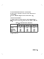
Americas
Brazil
(tel) (+55) 11 3351 7012
(fax) (+55) 11 3351 7024
Mexico
(tel) 1 800 254 2440
(fax) 1 800 254 4222
Canada
(tel) +1 877 894 4414
(fax) +1 303 662 3369
United States
(tel) 800 829 4444
(alt) (+1) 303 662 3998
(fax) 800 829 4433
Asia Pacific and Japan
Australia
(tel) 1 800 225 574
(fax) 1 800 681 776
(fax) 1 800 225 539
China
(tel) 800 810 0508
(alt) 800 810 0510
(fax) 800 810 0507
(fax) 800 810 0362
Hong Kong
(tel) 800 933 229
(fax) 800 900 701
India
(tel) 1600 112 626
(fax) 1600 112 727
(fax) 1600 113 040
Japan (Bench)
(tel) 0120 32 0119
(alt) (+81) 426 56 7799
(fax) 0120 01 2144
Japan (On-Site)
(tel) 0120 802 363
(alt) (+81) 426 56 7498
(fax) (+81) 426 60 8953
Singapore
(tel) 1 800 275 0880
(fax) (+65) 6755 1235
(fax) (+65) 6755 1214
South Korea
(tel) 080 778 0011
(fax) 080 778 0013
Taiwan
(tel) 0800 047 669
(fax) 0800 047 667
(fax) 886 3492 0779
Thailand
(tel) 1 800 2758 5822
(alt) (+66) 2267 5913
(fax) 1 800 656 336
Malaysia
(tel) 1800 880 399
(fax) 1800 801 054
Europe
Finland
(tel) (+358) 10 855 2100
(fax) (+358) (0) 10 855 2923
Austria
(tel) 0820 87 44 11*
(fax) 0820 87 44 22
Belgium
(tel) (+32) (0)2 404 9340
(alt) (+32) (0)2 404 9000
(fax) (+32) (0)2 404 9395
Denmark
(tel) (+45) 7013 1515
(alt) (+45) 7013 7313
(fax) (+45) 7013 1555
France
(tel) 0825 010 700*
(alt) (+33) (0)1 6453 5623
(fax) 0825 010 701*
Germany
(tel) 01805 24 6333*
(alt) 01805 24 6330*
(fax) 01805 24 6336*
Israel
Ireland
(tel) (+353) (0)1 890 924 204 (tel) (+972) 3 9288 500
(alt) (+353) (0)1 890 924 206 (fax) (+972) 3 9288 501
(fax)(+353) (0)1 890 924 024
Italy
(tel) (+39) (0)2 9260 8484
(fax) (+39) (0)2 9544 1175
Luxemburg
(tel) (+32) (0)2 404 9340
(alt) (+32) (0)2 404 9000
(fax) (+32) (0)2 404 9395
Netherlands
(tel) (+31) (0)20 547 2111
(alt) (+31) (0)20 547 2000
(fax) (+31) (0)20 547 2190
Russia
(tel) (+7) 095 797 3963
(alt) (+7) 095 797 3900
(fax) (+7) 095 797 3901
Spain
(tel) (+34) 91 631 3300
(alt) (+34) 91 631 3000
(fax) (+34) 91 631 3301
Sweden
(tel) 0200 88 22 55*
(alt) (+46) (0)8 5064 8686
(fax) 020 120 2266*
Switzerland (French)
(tel) 0800 80 5353 opt. 2*
(alt) (+33) (0)1 6453 5623
(fax) (+41) (0)22 567 5313
Switzerland (German)
(tel) 0800 80 5353 opt. 1*
(alt) (+49) (0)7031 464 6333
(fax) (+41) (0)1 272 7373
Switzerland (Italian)
(tel) 0800 80 5353 opt. 3*
(alt) (+39) (0)2 9260 8484
(fax) (+41) (0)22 567 5314
United Kingdom
(tel) (+44) (0)7004 666666
(alt) (+44) (0)7004 123123
(fax) (+44) (0)7004 444555
(tel) = primary telephone number; (alt) = alternate telephone number; (fax) = FAX number; * = in country number
11/16/04
Service Guide
HP 8752C Network Analyzer
ABCDE
HP Part No. 08752-90136
Supersedes December 1997
Printed in USA February 1998
Notice.
The information contained in this document is subject to change without notice.
Hewlett-Packard makes no warranty of any kind with regard to this material,
including but not limited to, the implied warranties of merchantability and
tness for a particular purpose. Hewlett-Packard shall not be liable for errors
contained herein or for incidental or consequential damages in connection with
the furnishing, performance, or use of this material.
c Copyright 1995, 1997, 1998 Hewlett-Packard Company
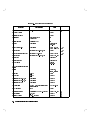
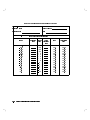
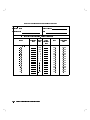
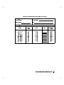
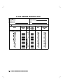
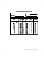
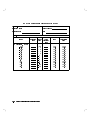
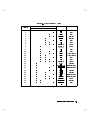
Contents
1. Service Equipment and Analyzer Options
Table of Service Test Equipment . . . . . . . . . . .
Principles of Microwave Connector Care . . . . . . .
Analyzer Options Available . . . . . . . . . . . . . .
Option 003, 3 GHz Operation . . . . . . . . . . . .
Option 004, Step Attenuator . . . . . . . . . . . .
Option 006, 6 GHz Operation . . . . . . . . . . . .
Option 010, Time Domain . . . . . . . . . . . . .
Option 075, 75
Impedance . . . . . . . . . . . . .
Option 1CM, Rack Mount Flange Kit Without Handles
Option 1CP, Rack Mount Flange Kit With Handles . .
Option AFN, add 50
Test Port Cable . . . . . . . .
Option AFP, add 75
Test Port Cable . . . . . . . .
Option B02, External Disk Drive . . . . . . . . . .
Service and Support Options . . . . . . . . . . . . .
.
.
.
.
.
.
.
.
.
.
.
.
.
.
.
.
.
.
.
.
.
.
.
.
.
.
.
.
.
.
.
.
.
.
.
.
.
.
.
.
.
.
.
.
.
.
.
.
.
.
.
.
.
.
.
.
.
.
.
.
.
.
.
.
.
.
.
.
.
.
1-1
1-5
1-7
1-7
1-7
1-7
1-7
1-7
1-7
1-8
1-8
1-8
1-8
1-9
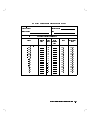
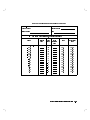
How to Test the Performance of Your Analyzer . . . . .
Sections in this Chapter . . . . . . . . . . . . . . . .
HP 8752C System Verication . . . . . . . . . . . . . .
Equipment . . . . . . . . . . . . . . . . . . . . .
Description . . . . . . . . . . . . . . . . . . . . .
System Verication Cycle and Kit Recertication . . . .
Measurement Uncertainty . . . . . . . . . . . . . .
Measurement Uncertainty Window . . . . . . . . . .
HP 8752C Type-N Test Port Characteristics (50
System)
Directivity . . . . . . . . . . . . . . . . . . . .
Source Match (Reection) . . . . . . . . . . . . .
Source Match (Transmission)* . . . . . . . . . . .
Reection Tracking . . . . . . . . . . . . . . . .
Load Match . . . . . . . . . . . . . . . . . . . .
Transmission Tracking . . . . . . . . . . . . . . .
.
.
.
.
.
.
.
.
.
.
.
.
.
.
.
.
.
.
.
.
.
.
.
.
.
.
.
.
.
.
.
.
.
.
.
.
.
.
.
.
.
.
.
.
.
.
.
.
.
.
.
.
.
.
.
.
.
.
.
.
2-1
2-2
2-3
2-3
2-3
2-4
2-4
2-4
2-6
2-6
2-6
2-6
2-6
2-7
2-7
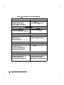
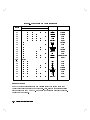
2. System Verication and Performance Tests
Contents-1
HP 8752C Type-N Test Port Characteristics (75
System) . . . .
Directivity . . . . . . . . . . . . . . . . . . . . . . . .
Source Match (Reection) . . . . . . . . . . . . . . . . .
Source Match (Transmission)* . . . . . . . . . . . . . . .
Reection Tracking . . . . . . . . . . . . . . . . . . . .
Load Match . . . . . . . . . . . . . . . . . . . . . . . .
Transmission Tracking . . . . . . . . . . . . . . . . . . .
System Verication Procedure . . . . . . . . . . . . . . . . .
In case of diculty . . . . . . . . . . . . . . . . . . . . .
HP 8752C Performance Tests . . . . . . . . . . . . . . . . . .
Equipment Required to Run the Performance Tests . . . . . .
1. Reection Test Port Output Frequency Range and Accuracy . .
Specications . . . . . . . . . . . . . . . . . . . . . . . .
Equipment . . . . . . . . . . . . . . . . . . . . . . . . .
Description . . . . . . . . . . . . . . . . . . . . . . . . .
Procedure . . . . . . . . . . . . . . . . . . . . . . . . . .
In case of diculty . . . . . . . . . . . . . . . . . . . . .
2. Reection Test Port Output Power Range and Level Linearity
(For HP 8752C Analyzers without Option 004) . . . . . . . .
Specications . . . . . . . . . . . . . . . . . . . . . . . .
Equipment . . . . . . . . . . . . . . . . . . . . . . . . .
Description . . . . . . . . . . . . . . . . . . . . . . . . .
Procedure . . . . . . . . . . . . . . . . . . . . . . . . . .
Power Range and Level Linearity for an HP 8752C or an HP
8752C Option 075 . . . . . . . . . . . . . . . . . . .
Power Range and Level Linearity for an HP 8752C with Option
003 . . . . . . . . . . . . . . . . . . . . . . . . . .
Power Range and Level Linearity for an HP 8752C with Options
003 and 075 . . . . . . . . . . . . . . . . . . . . . .
Power Range and Level Linearity for an HP 8752C with Option
006 . . . . . . . . . . . . . . . . . . . . . . . . . .
In case of diculty . . . . . . . . . . . . . . . . . . . .
3. Reection Test Port Output Power Range and Level Linearity (HP
8752C with Option 004) . . . . . . . . . . . . . . . . . . .
Specications . . . . . . . . . . . . . . . . . . . . . . . .
Equipment . . . . . . . . . . . . . . . . . . . . . . . . .
Description . . . . . . . . . . . . . . . . . . . . . . . . .
Procedure . . . . . . . . . . . . . . . . . . . . . . . . . .
Power Range for an HP 8752C with Option 004 . . . . . . .
Power Level Linearity for an HP 8752C with Option 004
or an HP 8752C withOptions 004 and 075 . . . . . . . .
Contents-2
2-7
2-7
2-7
2-8
2-8
2-8
2-8
2-9
2-10
2-11
2-12
2-13
2-13
2-13
2-13
2-14
2-14
2-15
2-15
2-15
2-15
2-16
2-16
2-17
2-18
2-18
2-18
2-19
2-19
2-19
2-19
2-20
2-20
2-21
Power Level Linearity for an HP 8752C with Options 003 and
004 . . . . . . . . . . . . . . . . . . . . . . . . . .
Power Level Linearity for an HP 8752C with Options 004 and
006 . . . . . . . . . . . . . . . . . . . . . . . . . .
Power Level Linearity for an HP 8752C with Options 003, 004,
and 075 . . . . . . . . . . . . . . . . . . . . . . . .
In case of diculty . . . . . . . . . . . . . . . . . . . .
4. Transmission Test Port Input Noise Floor Level (HP 8752C
without Option 075) . . . . . . . . . . . . . . . . . . . .
Specications . . . . . . . . . . . . . . . . . . . . . . . .
Equipment . . . . . . . . . . . . . . . . . . . . . . . . .
Description . . . . . . . . . . . . . . . . . . . . . . . . .
Procedure . . . . . . . . . . . . . . . . . . . . . . . . . .
Noise Floor Level at 300 kHz to 1.3 GHz (Standard Option), 300
kHz to 3 GHz (Option 003), or 300 kHz to 6 GHz (Option
006) with an IF BW of 3 kHz . . . . . . . . . . . . . .
Noise Floor Level at 300 kHz to 1.3 GHz (Standard Option) or
300 kHz to 3 GHz (Option 003) with an IF BW of 10 Hz . .
Noise Floor Level at 3 GHz to 6 GHz (Option 006) with an IF
BW of 10 Hz . . . . . . . . . . . . . . . . . . . . . .
Noise Floor Level at 3 GHz to 6 GHz (Option 006) with IF BW of
3 kHz . . . . . . . . . . . . . . . . . . . . . . . . .
In case of diculty . . . . . . . . . . . . . . . . . . . .
5. Transmission Test Port Input Noise Floor Level
(HP 8752C with Option 075) . . . . . . . . . . . . . . . . .
Specications . . . . . . . . . . . . . . . . . . . . . . . .
Equipment . . . . . . . . . . . . . . . . . . . . . . . . .
Description . . . . . . . . . . . . . . . . . . . . . . . . .
Procedure . . . . . . . . . . . . . . . . . . . . . . . . . .
Noise Floor Level at 300 kHz to 1.3 GHz (Option 075) or 300
kHz to3 GHz (Options 075 and 003) with an IF BW of 3 kHz
Noise Floor Level at 300 kHz to 1.3 GHz (Option 075) or 300
kHz to3 GHz (Options 075 and 003) with an IF BW of 10 Hz
In case of diculty . . . . . . . . . . . . . . . . . . . .
6. Test Port Crosstalk . . . . . . . . . . . . . . . . . . . . .
Specications . . . . . . . . . . . . . . . . . . . . . . . .
Equipment . . . . . . . . . . . . . . . . . . . . . . . . .
Description . . . . . . . . . . . . . . . . . . . . . . . . .
Procedure . . . . . . . . . . . . . . . . . . . . . . . . . .
Test Port Crosstalk for a Standard HP 8752C or an HP 8752C
with Option 003 . . . . . . . . . . . . . . . . . . . .
2-22
2-23
2-23
2-23
2-24
2-24
2-24
2-24
2-24
2-24
2-26
2-27
2-28
2-28
2-29
2-29
2-29
2-29
2-29
2-29
2-31
2-31
2-32
2-32
2-32
2-32
2-33
2-33
Contents-3
Test Port Crosstalk for an HP 8752C with Option 006 . . . . .
Test Port Crosstalk for an HP 8752C with Option 075 . . . . .
Test Port Crosstalk for an HP 8752C with Options 003 and 075
In case of diculty . . . . . . . . . . . . . . . . . . . .
7. System Trace Noise . . . . . . . . . . . . . . . . . . . . .
Specications . . . . . . . . . . . . . . . . . . . . . . . .
Equipment . . . . . . . . . . . . . . . . . . . . . . . . .
Description . . . . . . . . . . . . . . . . . . . . . . . . .
Procedure . . . . . . . . . . . . . . . . . . . . . . . . . .
Reection Trace Noise (Magnitude) . . . . . . . . . . . . .
Reection Trace Noise (Phase) . . . . . . . . . . . . . . .
Transmission Trace Noise (Magnitude) . . . . . . . . . . . .
Transmission Trace Noise (Phase) . . . . . . . . . . . . . .
In case of diculty . . . . . . . . . . . . . . . . . . . .
8. Magnitude Dynamic Accuracy (HP 8752C - All Options) . . . .
Specications . . . . . . . . . . . . . . . . . . . . . . . .
Equipment . . . . . . . . . . . . . . . . . . . . . . . . .
Description . . . . . . . . . . . . . . . . . . . . . . . . .
Procedure . . . . . . . . . . . . . . . . . . . . . . . . . .
In case of diculty . . . . . . . . . . . . . . . . . . . .
9. Phase Dynamic Accuracy (HP 8752C - All Options) . . . . . .
Specications . . . . . . . . . . . . . . . . . . . . . . . .
Equipment . . . . . . . . . . . . . . . . . . . . . . . . .
Description . . . . . . . . . . . . . . . . . . . . . . . . .
Procedure . . . . . . . . . . . . . . . . . . . . . . . . . .
10. Compression . . . . . . . . . . . . . . . . . . . . . . . .
Specications . . . . . . . . . . . . . . . . . . . . . . . .
Equipment . . . . . . . . . . . . . . . . . . . . . . . . .
Description . . . . . . . . . . . . . . . . . . . . . . . . .
Procedure . . . . . . . . . . . . . . . . . . . . . . . . . .
In case of diculty . . . . . . . . . . . . . . . . . . . .
Performance Test Record . . . . . . . . . . . . . . . . . . . .
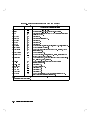
3. Adjustments and Correction Constants
When to Perform the Adjustment Procedures . . .
Keep Correction Constants Current to Save Time
Adjustment Procedure Error Messages . . . . .
Perform Adjustments in This Order . . . . . . . .
Test Equipment Specications . . . . . . . . .
Analyzer Cover Removal . . . . . . . . . . . .
1. A9 CC Jumper Position Procedure . . . . . . .
Contents-4
.
.
.
.
.
.
.
.
.
.
.
.
.
.
.
.
.
.
.
.
.
.
.
.
.
.
.
.
.
.
.
.
.
.
.
.
.
.
.
.
.
.
.
.
.
.
.
.
.
2-33
2-34
2-34
2-35
2-36
2-36
2-36
2-36
2-37
2-37
2-38
2-38
2-39
2-39
2-40
2-40
2-40
2-41
2-41
2-44
2-45
2-45
2-45
2-45
2-46
2-47
2-47
2-47
2-47
2-48
2-49
2-50
3-1
3-1
3-1
3-2
3-3
3-4
3-5
A9 CC (Correction Constant) Jumper Position . . . . . . . . .
Procedure . . . . . . . . . . . . . . . . . . . . . . . . . .
2. Source Default Correction Constants (Test #44) . . . . . . . .
Equipment . . . . . . . . . . . . . . . . . . . . . . . . .
Warm-up time . . . . . . . . . . . . . . . . . . . . . . .
Description and Procedure . . . . . . . . . . . . . . . . . .
3. Source Pretune Default Correction Constants (Test #45) . . . .
Equipment . . . . . . . . . . . . . . . . . . . . . . . . .
Warm-up time . . . . . . . . . . . . . . . . . . . . . . .
Description and Procedure . . . . . . . . . . . . . . . . . .
4. Analog Bus Correction Constants (Test #46) . . . . . . . . . .
Equipment . . . . . . . . . . . . . . . . . . . . . . . . .
Warm-up time . . . . . . . . . . . . . . . . . . . . . . .
Description and Procedure . . . . . . . . . . . . . . . . . .
5. RF Output Power Correction Constants (Test #47) . . . . . . .
Equipment Required . . . . . . . . . . . . . . . . . . . . .
Warm-up time . . . . . . . . . . . . . . . . . . . . . . .
Description and Procedure . . . . . . . . . . . . . . . . . .
Power Sensor Calibration Factor Entry . . . . . . . . . . . .
Source Correction Routine . . . . . . . . . . . . . . . . . .
6. Source Pretune Correction Constants (Test #48) . . . . . . . .
Equipment Required . . . . . . . . . . . . . . . . . . . . .
Warm-up time . . . . . . . . . . . . . . . . . . . . . . .
Description and Procedure . . . . . . . . . . . . . . . . . .
7. Display Intensity Adjustments (Test #49) . . . . . . . . . . .
Equipment Required . . . . . . . . . . . . . . . . . . . . .
Warm-up time . . . . . . . . . . . . . . . . . . . . . . .
Description and Procedure . . . . . . . . . . . . . . . . . .
Background Adjustment . . . . . . . . . . . . . . . . . . .
Maximum Intensity Adjustment . . . . . . . . . . . . . . . .
Operating Default Intensity Adjustment . . . . . . . . . . . .
8. IF Amplier Correction Constants (Test #51) . . . . . . . . .
Equipment Required . . . . . . . . . . . . . . . . . . . . .
Warm-up time . . . . . . . . . . . . . . . . . . . . . . .
Description and Procedure . . . . . . . . . . . . . . . . . .
9. ADC Oset Correction Constants (Test #52) . . . . . . . . . .
Equipment . . . . . . . . . . . . . . . . . . . . . . . . .
Warm-up time . . . . . . . . . . . . . . . . . . . . . . .
Description and Procedure . . . . . . . . . . . . . . . . . .
10. Frequency Response Correction Constants (Tests #53 and #57)
Equipment Required . . . . . . . . . . . . . . . . . . . . .
3-5
3-5
3-8
3-8
3-8
3-8
3-9
3-9
3-9
3-9
3-10
3-10
3-10
3-10
3-11
3-11
3-11
3-11
3-12
3-13
3-14
3-14
3-14
3-14
3-15
3-15
3-15
3-15
3-15
3-16
3-18
3-19
3-19
3-19
3-19
3-21
3-21
3-21
3-21
3-22
3-22
Contents-5
Warm-up time . . . . . . . . . . . . . . . . . . . . . . .
Description and Procedure . . . . . . . . . . . . . . . . . .
11. Cavity Oscillator Frequency Correction Constants (Test #54) .
Equipment Required . . . . . . . . . . . . . . . . . . . . .
Warm-up time . . . . . . . . . . . . . . . . . . . . . . .
Description and Procedure . . . . . . . . . . . . . . . . . .
Spur Search Procedure with Filter . . . . . . . . . . . . . .
Spur Search Procedure without Filter . . . . . . . . . . . . .
12. Serial Number Correction Constant (Test #55) . . . . . . . .
Equipment . . . . . . . . . . . . . . . . . . . . . . . . .
Warm-up time . . . . . . . . . . . . . . . . . . . . . . .
Description and Procedure . . . . . . . . . . . . . . . . . .
13. Option Numbers Correction Constant (Test #56) . . . . . . .
Equipment . . . . . . . . . . . . . . . . . . . . . . . . .
Warm-up time . . . . . . . . . . . . . . . . . . . . . . .
Description and Procedure . . . . . . . . . . . . . . . . . .
Option 004 Installation . . . . . . . . . . . . . . . . . . .
14. Initialize EEPROMs (Test #58) . . . . . . . . . . . . . . . .
15. EEPROM Backup Disk Procedure . . . . . . . . . . . . . .
Equipment Required . . . . . . . . . . . . . . . . . . . . .
Warm-up time . . . . . . . . . . . . . . . . . . . . . . .
Description and Procedure . . . . . . . . . . . . . . . . . .
How to Make an EEPROM Backup Disk and Store CCs and Data
to It . . . . . . . . . . . . . . . . . . . . . . . . . . .
How to Recall CC Data from the EEPROM Disk into the Analyzer
16. Model Number Correction Constant (Option 075 Only) . . . .
Equipment . . . . . . . . . . . . . . . . . . . . . . . . .
Warmup time . . . . . . . . . . . . . . . . . . . . . . .
Description and Procedure . . . . . . . . . . . . . . . . . .
17. Vertical Position and Focus Adjustments . . . . . . . . . . .
Equipment . . . . . . . . . . . . . . . . . . . . . . . . .
Warmup time . . . . . . . . . . . . . . . . . . . . . . .
Description and Procedure . . . . . . . . . . . . . . . . . .
Vertical Position Adjustment . . . . . . . . . . . . . . . . .
Focus Adjustment . . . . . . . . . . . . . . . . . . . . . .
18. Display Degaussing (Demagnetizing) . . . . . . . . . . . . .
Equipment . . . . . . . . . . . . . . . . . . . . . . . . .
Warm-up time . . . . . . . . . . . . . . . . . . . . . . .
Description and Procedure . . . . . . . . . . . . . . . . . .
19. Fractional-N Frequency Range Adjustment . . . . . . . . .
Equipment Required . . . . . . . . . . . . . . . . . . . . .
Contents-6
3-22
3-22
3-24
3-24
3-24
3-24
3-26
3-28
3-32
3-32
3-32
3-32
3-34
3-34
3-34
3-35
3-36
3-37
3-38
3-38
3-38
3-38
3-39
3-40
3-42
3-42
3-42
3-42
3-43
3-43
3-43
3-43
3-43
3-44
3-45
3-45
3-45
3-45
3-46
3-46
Warm-up time . . . . . . . . . . . . . . . . . . . . .
Description and Procedure . . . . . . . . . . . . . . . .
20. Frequency Accuracy Adjustment . . . . . . . . . . . .
Equipment Required . . . . . . . . . . . . . . . . . . .
Warm-up time . . . . . . . . . . . . . . . . . . . . .
Description and Procedure . . . . . . . . . . . . . . . .
21. High/Low Band Transition Adjustment . . . . . . . . .
Equipment Required . . . . . . . . . . . . . . . . . . .
Warm-up time . . . . . . . . . . . . . . . . . . . . .
Description and Procedure . . . . . . . . . . . . . . . .
22. Fractional-N Spur Avoidance and FM Sideband Adjustment
Equipment Required . . . . . . . . . . . . . . . . . . .
Warmup time . . . . . . . . . . . . . . . . . . . . .
Description and Procedure . . . . . . . . . . . . . . .
23. Source Spur Avoidance Tracking Adjustment . . . . . .
Equipment Required . . . . . . . . . . . . . . . . . . .
Warm-up time . . . . . . . . . . . . . . . . . . . . .
Description and Procedure . . . . . . . . . . . . . . . .
4. Start Troubleshooting Here
Assembly Replacement Sequence . . . . . . . . . .
Having Your Analyzer Serviced . . . . . . . . . . .
Step 1. Initial Observations . . . . . . . . . . . . .
Initiate the Analyzer Self-Test . . . . . . . . . .
If the Self-Test Failed . . . . . . . . . . . . .
Step 2. Condence Test . . . . . . . . . . . . . .
Procedure . . . . . . . . . . . . . . . . . . . .
Cable Condence Test . . . . . . . . . . . . . .
Procedure . . . . . . . . . . . . . . . . . . .
Step 3. HP-IB Systems Check . . . . . . . . . . . .
If Using a Plotter or Printer . . . . . . . . . . .
If Using an External Disk Drive . . . . . . . . . .
Troubleshooting Systems with Multiple Peripherals .
Troubleshooting Systems with Controllers . . . . .
Step 4. Faulty Group Isolation . . . . . . . . . . .
Power Supply Check . . . . . . . . . . . . . . .
Check the Rear Panel LEDs . . . . . . . . . . .
Check the A8 Post Regulator LEDs . . . . . . .
Digital Control Check . . . . . . . . . . . . . .
Observe the Power Up Sequence . . . . . . . .
Verify Internal Tests Passed . . . . . . . . . . .
.
.
.
.
.
.
.
.
.
.
.
.
.
.
.
.
.
.
.
.
.
.
.
.
.
.
.
.
.
.
.
.
.
.
.
.
.
.
.
.
.
.
.
.
.
.
.
.
.
.
.
.
.
.
.
.
.
.
.
.
.
.
.
.
.
.
.
.
.
.
.
.
.
.
.
.
.
.
.
.
.
.
.
.
.
.
.
.
.
.
.
.
.
.
.
.
.
.
.
.
.
.
.
.
.
.
.
.
.
.
.
.
.
.
.
.
.
.
.
.
3-46
3-46
3-49
3-49
3-49
3-50
3-51
3-51
3-51
3-51
3-54
3-54
3-54
3-54
3-58
3-58
3-58
3-58
.
.
.
.
.
.
.
.
.
.
.
.
.
.
.
.
.
.
.
.
.
.
.
.
.
.
.
.
.
.
.
.
.
.
.
.
.
.
.
.
.
.
4-2
4-2
4-3
4-3
4-3
4-4
4-4
4-5
4-5
4-7
4-8
4-8
4-9
4-9
4-10
4-11
4-11
4-11
4-12
4-12
4-13
Contents-7
Source Check . . . . . . . . . . . . . . . . . . . . . . . .
Receiver Check . . . . . . . . . . . . . . . . . . . . . . .
Accessories Check . . . . . . . . . . . . . . . . . . . . . .
5. Power Supply Troubleshooting
Assembly Replacement Sequence . . . . . . . . .
Simplied Block Diagram . . . . . . . . . . . . .
Start Here . . . . . . . . . . . . . . . . . . . .
Check the Green LED and Red LED on A15 . . .
Check the Green LEDs on A8 . . . . . . . . . .
Measure the Post Regulator Voltages . . . . . .
If the Green LED on A15 is not On Steadily . . . .
Check the Line Voltage, Selector Switch, and Fuse
If the Red LED On A15 is On . . . . . . . . . . .
Check the A8 Post Regulator . . . . . . . . . .
Verify the A15 Preregulator . . . . . . . . . .
Check for a Faulty Assembly . . . . . . . . . .
Check the Operating Temperature . . . . . . .
Inspect the Motherboard . . . . . . . . . . . .
If the Green LEDs On A8 are not All On . . . . .
Remove A8, Maintain A15W1 Cable Connection .
Check the A8 Fuses and Voltages . . . . . . . .
Remove the Assemblies . . . . . . . . . . . .
Briey Disable the Shutdown Circuitry . . . . .
Inspect the Motherboard . . . . . . . . . . . .
Error Messages . . . . . . . . . . . . . . . . .
Check the Fuses and Isolate A8 . . . . . . . . .
Fan Troubleshooting . . . . . . . . . . . . . . .
Fan Speeds . . . . . . . . . . . . . . . . . .
Check the Fan Voltages . . . . . . . . . . . . .
Short A8TP3 to Ground . . . . . . . . . . . .
Intermittent Problems . . . . . . . . . . . . . .
6. Digital Control Troubleshooting
Assembly Replacement Sequence . . . . .
Digital Control Group Block Diagram . . .
Check A9 CPU Operation . . . . . . . . .
A9 CC Jumper Positions . . . . . . . .
Checking A9 CPU Red LED Patterns . .
Check A19 GSP and A18 Display Operation
Cycle Power and Look at the Display . .
Contents-8
.
.
.
.
.
.
.
.
.
.
.
.
.
.
.
.
.
.
.
.
.
.
.
.
.
.
.
.
4-13
4-15
4-15
.
.
.
.
.
.
.
.
.
.
.
.
.
.
.
.
.
.
.
.
.
.
.
.
.
.
.
.
.
.
.
.
.
.
.
.
.
.
.
.
.
.
.
.
.
.
.
.
.
.
.
.
.
.
.
.
.
.
.
.
.
.
.
.
.
.
.
.
.
.
.
.
.
.
.
.
.
.
.
.
.
.
.
.
.
.
.
.
.
.
.
.
.
.
.
.
.
.
.
.
.
.
.
.
.
.
.
.
.
.
.
.
.
.
.
.
.
.
.
.
.
.
.
.
.
.
.
.
.
.
.
.
.
.
.
.
.
.
.
.
.
.
.
.
.
.
.
.
.
.
.
.
.
.
.
.
.
.
.
.
.
.
.
.
.
.
.
.
.
.
.
.
.
.
.
.
.
.
.
.
.
.
.
.
.
.
.
.
.
5-2
5-3
5-4
5-4
5-5
5-5
5-7
5-7
5-8
5-8
5-9
5-11
5-13
5-13
5-14
5-14
5-14
5-15
5-16
5-18
5-19
5-21
5-22
5-22
5-22
5-22
5-23
.
.
.
.
.
.
.
.
.
.
.
.
.
.
.
.
.
.
.
.
.
.
.
.
.
.
.
.
.
.
.
.
.
.
.
.
.
.
.
.
.
.
.
.
.
.
.
.
.
6-2
6-3
6-4
6-4
6-5
6-7
6-7
Perform Display Intensity and Focus Adjustments . .
A1/A2 Front Panel Troubleshooting . . . . . . . . . .
Check Front Panel LEDs After Preset . . . . . . . .
Identify the Stuck Key . . . . . . . . . . . . . . .
Inspect Cables . . . . . . . . . . . . . . . . . . .
Test Using a Controller . . . . . . . . . . . . . . .
Run the Internal Diagnostic Tests . . . . . . . . . . .
A19 GSP and A18 Display Troubleshooting . . . . . .
Measure Display Power Supply Voltages on A19 . . .
Measure Display Power Supply Voltages Entering A19
Run Display Test 59 . . . . . . . . . . . . . . . .
Inspect Ribbon Cable Repeat Display Test 59 . . . . .
Perform Walking One Pattern . . . . . . . . . . . .
Run display Tests 60-65 . . . . . . . . . . . . . .
If the Fault is Intermittent . . . . . . . . . . . . . .
Repeat Test Function . . . . . . . . . . . . . . . .
HP-IB Failures . . . . . . . . . . . . . . . . . . . .
.
.
.
.
.
.
.
.
.
.
.
.
.
.
.
.
.
6-7
6-7
6-7
6-8
6-10
6-11
6-11
6-13
6-13
6-14
6-15
6-15
6-16
6-17
6-18
6-18
6-18
Assembly Replacement Sequence . . . . . . . . . . . . . . . .
Before You Start Troubleshooting . . . . . . . . . . . . . . . .
Power . . . . . . . . . . . . . . . . . . . . . . . . . . . . .
1. Source Default Correction Constants (Test 44) . . . . . . . .
2. RF Output Power Correction Constants (Test 47) . . . . . .
3. Sampler Magnitude and Phase Correction Constants (Test 53)
Phase Lock Error . . . . . . . . . . . . . . . . . . . . . . .
Phase Lock Loop Error Message Check . . . . . . . . . . . .
A4 Sampler/Mixer Check . . . . . . . . . . . . . . . . . . .
A3 Source and A11 Phase Lock Check . . . . . . . . . . . .
YO Coil Drive Check with Analog Bus . . . . . . . . . . . .
YO Coil Drive Check with Oscilloscope . . . . . . . . . . .
A12 Reference Check . . . . . . . . . . . . . . . . . . . .
Analog Bus Method . . . . . . . . . . . . . . . . . . . .
Oscilloscope Method . . . . . . . . . . . . . . . . . . . .
100 kHz Pulses . . . . . . . . . . . . . . . . . . . . . .
PLREF Waveforms . . . . . . . . . . . . . . . . . . . . .
REF Signal At A11TP1 PIN 9 . . . . . . . . . . . . . . .
High Band REF Signal . . . . . . . . . . . . . . . . . .
Low Band REF Signal . . . . . . . . . . . . . . . . . .
FN LO at A12 Check . . . . . . . . . . . . . . . . . . . .
4 MHz Reference Signal . . . . . . . . . . . . . . . . . .
7-2
7-2
7-3
7-3
7-3
7-3
7-4
7-4
7-6
7-8
7-11
7-12
7-13
7-13
7-15
7-16
7-17
7-17
7-17
7-18
7-19
7-20
7. Source Troubleshooting
.
.
.
.
.
.
.
.
.
.
.
.
.
.
.
.
.
.
.
.
.
.
.
.
.
.
.
.
.
.
.
.
.
.
.
.
.
.
.
.
.
.
.
.
.
.
.
.
.
.
.
.
.
.
.
.
.
.
.
.
.
.
.
.
.
.
.
.
Contents-9
2ND LO Waveforms . . . . . . . . . . . . . . . . . .
90 Degree Phase Oset of 2nd LO Signals in High Band
In-Phase 2nd LO Signals in Low Band . . . . . . . . .
A12 Digital Control Signals Check . . . . . . . . . . . .
L ENREF Line . . . . . . . . . . . . . . . . . . . .
L HB and L LB Lines . . . . . . . . . . . . . . . . .
A13/A14 Fractional-N Check . . . . . . . . . . . . . . .
Fractional-N Check with Analog Bus . . . . . . . . . .
A14 VCO Range Check with Oscilloscope . . . . . . . .
A14 VCO Exercise . . . . . . . . . . . . . . . . . . .
A14 Divide-by-N Circuit Check . . . . . . . . . . . . .
A14-to-A13 Digital Control Signals Check. . . . . . . . .
H MB Line . . . . . . . . . . . . . . . . . . . . .
A7 Pulse Generator Check . . . . . . . . . . . . . . . .
A7 Pulse Generator Check with Spectrum Analyzer . . .
Rechecking the A13/A14 Fractional-N . . . . . . . . . .
A7 Pulse Generator Check with Oscilloscope . . . . . . .
A11 Phase Lock Check . . . . . . . . . . . . . . . . . .
Phase Lock Check with PLL DIAG . . . . . . . . . . .
Phase Lock Check by Signal Examination . . . . . . . .
Source Group Troubleshooting Appendix . . . . . . . . . .
Troubleshooting Source Problems with the Analog Bus . . .
Phase Lock Diagnostic Tools . . . . . . . . . . . . . . .
Phase Lock Error Messages . . . . . . . . . . . . . . .
Phase Lock Diagnostic Routines . . . . . . . . . . . . .
Broadband Power Problems . . . . . . . . . . . . . . .
8. Receiver Troubleshooting
Assembly Replacement Sequence . . . . . . . . . . .
Receiver Failure Error Messages . . . . . . . . . . .
CAUTION: OVERLOAD ON REFL PORT, POWER REDUCED .
CAUTION: OVERLOAD ON TRANS PORT, POWER REDUCED .
Check the R, A, and B Inputs . . . . . . . . . . . . .
Troubleshooting When All Inputs Look Bad . . . . . .
Run Internal Tests 18 and 17 . . . . . . . . . . . .
Check the 4 MHz REF Signal . . . . . . . . . . . . .
Check A10 by Substitution or Signal Examination . .
Troubleshooting When One or More Inputs Look Good .
Check the Frequency Response Correction . . . . .
Check the 4 kHz Signal . . . . . . . . . . . . . . .
Check 1st LO Signal at Sampler/Mixer . . . . . . . .
Contents-10
.
.
.
.
.
.
.
.
.
.
.
.
.
.
.
.
.
.
.
.
.
.
.
.
.
.
.
.
.
.
.
.
.
.
.
.
.
.
.
.
.
.
.
.
.
.
.
.
.
.
.
.
.
.
.
.
.
.
.
.
.
.
.
.
.
.
.
.
.
.
.
.
.
.
.
.
.
.
.
.
.
.
.
.
.
.
.
.
.
.
.
7-21
7-21
7-22
7-23
7-23
7-24
7-24
7-24
7-26
7-28
7-29
7-30
7-32
7-33
7-33
7-35
7-35
7-37
7-37
7-37
7-39
7-39
7-39
7-39
7-40
7-40
.
.
.
.
.
.
.
.
.
.
.
.
.
.
.
.
.
.
.
.
.
.
.
.
.
.
8-2
8-2
8-2
8-3
8-4
8-7
8-7
8-8
8-8
8-11
8-11
8-11
8-12
Check 2nd LO Signal at Sampler/Mixer . . . . . . . . . . . .
Check Input Trace . . . . . . . . . . . . . . . . . . . . . .
9. Accessories Troubleshooting
Assembly Replacement Sequence . . . . . . . . . . . .
Inspect the Accessories . . . . . . . . . . . . . . . . .
Inspect the Test Port Connectors and Calibration Devices
Inspect the Error Terms . . . . . . . . . . . . . . . .
Cable Test . . . . . . . . . . . . . . . . . . . . . .
Verify Shorts and Opens . . . . . . . . . . . . . . .
10. Service Key Menus and Error Messages
Service Key Menus . . . . . . . . . . .
Error Messages . . . . . . . . . . . .
Service Key Menus - Internal Diagnostics
Tests Menu . . . . . . . . . . . . .
Test Options Menu . . . . . . . . . .
Self Diagnose Softkey . . . . . . . .
Test Descriptions . . . . . . . . . . .
Internal Tests . . . . . . . . . . .
External Tests . . . . . . . . . . .
System Verication Tests . . . . . .
Adjustment Tests . . . . . . . . .
Display Tests . . . . . . . . . . .
Test Patterns . . . . . . . . . . .
Service Key Menus - Service Features . .
Service Modes Menu . . . . . . . . .
Service Modes More Menu . . . . . .
Analog Bus . . . . . . . . . . . . .
Description of the Analog Bus . . .
The Main ADC . . . . . . . . . . .
The Frequency Counter . . . . . .
Analog In Menu . . . . . . . . . . .
Analog Bus Nodes . . . . . . . . . .
A3 Source . . . . . . . . . . . . .
A10 Digital IF . . . . . . . . . . .
A11 Phase Lock . . . . . . . . . .
A12 Reference . . . . . . . . . . .
A14 Fractional-N (Digital) . . . . .
PEEK/POKE Menu . . . . . . . . . .
Firmware Revision Softkey . . . . . . .
.
.
.
.
.
.
.
.
.
.
.
.
.
.
.
.
.
.
.
.
.
.
.
.
.
.
.
.
.
.
.
.
.
.
.
.
.
.
.
.
.
.
.
.
.
.
.
.
.
.
.
.
.
.
.
.
.
.
.
.
.
.
.
.
.
.
.
.
.
.
.
.
.
.
.
.
.
.
.
.
.
.
.
.
.
.
.
.
.
.
.
.
.
.
.
.
.
.
.
.
.
.
.
.
.
.
.
.
.
.
.
.
.
.
.
.
.
.
.
.
.
.
.
.
.
.
.
.
.
.
.
.
.
.
.
.
.
.
.
.
.
.
.
.
.
.
.
.
.
.
.
.
.
.
.
.
.
.
.
.
.
.
.
.
.
.
.
.
.
.
.
.
.
.
.
.
.
.
.
.
.
.
.
.
.
.
.
.
.
.
.
.
.
.
.
.
.
.
.
.
.
.
.
.
.
.
.
.
.
.
.
.
.
.
.
.
.
.
.
.
.
.
.
.
.
.
.
.
.
.
.
.
8-13
8-14
.
.
.
.
.
.
.
.
.
.
.
.
.
.
.
.
.
.
.
.
.
.
.
.
9-2
9-3
9-3
9-3
9-5
9-6
.
.
.
.
.
.
.
.
.
.
.
.
.
.
.
.
.
.
.
.
.
.
.
.
.
.
.
.
.
.
.
.
.
.
.
.
.
.
.
.
.
.
.
.
.
.
.
.
.
.
.
.
.
.
.
.
.
.
.
.
.
.
.
.
.
.
.
.
.
.
.
.
.
.
.
.
.
.
.
.
.
.
.
.
.
.
.
.
.
.
.
.
.
.
.
.
.
.
.
.
.
.
.
.
.
.
.
.
.
.
.
.
.
.
.
.
10-1
10-1
10-2
10-3
10-5
10-7
10-7
10-7
10-12
10-13
10-14
10-16
10-17
10-19
10-20
10-23
10-25
10-25
10-25
10-25
10-27
10-29
10-29
10-36
10-37
10-44
10-47
10-50
10-51
Contents-11
HP-IB Service Mnemonic Denitions
Invoking Tests Remotely . . . . .
Analog Bus Codes . . . . . . . .
Error Messages . . . . . . . . . .
.
.
.
.
.
.
.
.
10-52
10-52
10-53
10-54
Error Terms Can Also Serve a Diagnostic Purpose . . . . . . .
Reection 1-Port Error-Correction Procedure . . . . . . . . .
Response and Isolation Calibration Procedures . . . . . . . . .
Error Term Inspection . . . . . . . . . . . . . . . . . . . .
If Error Terms Seem Worse than Typical Values . . . . . . .
Uncorrected Performance . . . . . . . . . . . . . . . . .
Error Term Descriptions . . . . . . . . . . . . . . . . . . .
Directivity (ED ) - After a Reection 1-Port Calibration . . . .
Description . . . . . . . . . . . . . . . . . . . . . . .
Signicant System Components . . . . . . . . . . . . . .
Aected Measurements . . . . . . . . . . . . . . . . .
Procedure . . . . . . . . . . . . . . . . . . . . . . . .
Source Match (ES ) - After a Reection 1-Port Calibration . . .
Description . . . . . . . . . . . . . . . . . . . . . . .
Signicant System Components . . . . . . . . . . . . . .
Aected Measurements . . . . . . . . . . . . . . . . .
Procedure . . . . . . . . . . . . . . . . . . . . . . . .
Reection Tracking (ER ) - After a Reection 1-Port Calibration
Description . . . . . . . . . . . . . . . . . . . . . . .
Signicant System Components . . . . . . . . . . . . . .
Aected Measurements . . . . . . . . . . . . . . . . .
Procedure . . . . . . . . . . . . . . . . . . . . . . . .
Isolation (Crosstalk, EX ) - After a Response and Isolation
(Transmission) Calibration . . . . . . . . . . . . . . . .
Description . . . . . . . . . . . . . . . . . . . . . . .
Signicant System Components . . . . . . . . . . . . . .
Aected Measurements . . . . . . . . . . . . . . . . .
Procedure . . . . . . . . . . . . . . . . . . . . . . . .
Transmission Tracking (ET ) . . . . . . . . . . . . . . . . .
Description . . . . . . . . . . . . . . . . . . . . . . .
Signicant System Components . . . . . . . . . . . . . .
Aected Measurements . . . . . . . . . . . . . . . . .
Procedure . . . . . . . . . . . . . . . . . . . . . . . .
.
.
.
.
.
.
.
.
.
.
.
.
.
.
.
.
.
.
.
.
.
.
11-2
11-4
11-6
11-8
11-9
11-9
11-10
11-11
11-11
11-11
11-11
11-11
11-13
11-13
11-13
11-13
11-13
11-15
11-15
11-15
11-15
11-15
.
.
.
.
.
.
.
.
.
.
11-17
11-17
11-17
11-17
11-17
11-19
11-19
11-19
11-19
11-19
11. Error Terms
Contents-12
.
.
.
.
.
.
.
.
.
.
.
.
.
.
.
.
.
.
.
.
.
.
.
.
.
.
.
.
.
.
.
.
.
.
.
.
.
.
.
.
.
.
.
.
.
.
.
.
12. Theory of Operation
How the HP 8752C Works . . . . . . . . . . . . . .
The Built-In Synthesized Source . . . . . . . . . .
The Source Step Attenuator (Option 004) . . . . .
The Built-In Transmission/Reection Test Set . . . .
The Receiver Block . . . . . . . . . . . . . . . .
The Microprocessor . . . . . . . . . . . . . . .
A Close Look at the Analyzer's Functional Groups . . .
Power Supply Theory . . . . . . . . . . . . . . . .
A15 Preregulator . . . . . . . . . . . . . . . . .
Line Power Module . . . . . . . . . . . . . . .
Preregulated Voltages . . . . . . . . . . . . . .
Regulated +5V Digital Supply . . . . . . . . . .
Shutdown Indications: the Green LED and Red LED
A8 Post Regulator . . . . . . . . . . . . . . . . .
Voltage Indications: the Green LEDs . . . . . . .
Shutdown Circuit . . . . . . . . . . . . . . . .
Variable Fan Circuit and Air Flow Detector . . . .
Display Power . . . . . . . . . . . . . . . . . .
Probe Power . . . . . . . . . . . . . . . . . .
Digital Control Theory . . . . . . . . . . . . . . . .
A1 Front Panel Keyboard . . . . . . . . . . . . .
A2 Front Panel Processor . . . . . . . . . . . . . .
A9 CPU/A10 Digital IF . . . . . . . . . . . . . . .
Main CPU . . . . . . . . . . . . . . . . . . . .
Main RAM . . . . . . . . . . . . . . . . . . . .
EEPROM . . . . . . . . . . . . . . . . . . . .
Digital Signal Processor . . . . . . . . . . . . .
A18 Display . . . . . . . . . . . . . . . . . . . .
A19 GSP . . . . . . . . . . . . . . . . . . . . .
A16 Rear Panel . . . . . . . . . . . . . . . . . .
Source Theory Overview . . . . . . . . . . . . . . .
A14/A13 Fractional-N . . . . . . . . . . . . . . .
A12 Reference . . . . . . . . . . . . . . . . . . .
A7 Pulse Generator . . . . . . . . . . . . . . . .
A11 Phase Lock . . . . . . . . . . . . . . . . . .
A3 Source . . . . . . . . . . . . . . . . . . . . .
Source Low Band Operation . . . . . . . . . . . . .
Source High Band Operation . . . . . . . . . . . . .
Signal Separation . . . . . . . . . . . . . . . . . .
The A30 Dual Directional Coupler . . . . . . . . .
.
.
.
.
.
.
.
.
.
.
.
.
.
.
.
.
.
.
.
.
.
.
.
.
.
.
.
.
.
.
.
.
.
.
.
.
.
.
.
.
.
.
.
.
.
.
.
.
.
.
.
.
.
.
.
.
.
.
.
.
.
.
.
.
.
.
.
.
.
.
.
.
.
.
.
.
.
.
.
.
.
.
.
.
.
.
.
.
.
.
.
.
.
.
.
.
.
.
.
.
.
.
.
.
.
.
.
.
.
.
.
.
.
.
.
.
.
.
.
.
.
.
.
.
.
.
.
.
.
.
.
.
.
.
.
.
.
.
.
.
.
.
.
.
.
.
.
.
.
.
.
.
.
.
.
.
.
.
.
.
.
.
.
.
.
.
.
.
.
.
.
.
.
.
.
.
.
.
.
.
.
.
.
.
.
.
.
.
.
.
.
.
.
.
.
.
.
.
.
.
12-2
12-3
12-3
12-4
12-4
12-4
12-5
12-6
12-6
12-7
12-7
12-7
12-7
12-8
12-8
12-8
12-8
12-9
12-9
12-9
12-10
12-11
12-11
12-11
12-11
12-12
12-12
12-12
12-12
12-13
12-14
12-14
12-14
12-14
12-15
12-15
12-16
12-19
12-23
12-23
Contents-13
Receiver Theory . . . . . . . . . . .
A4/A5/A6 Sampler/Mixer . . . . . .
The Sampler Circuit in High Band .
The Sampler Circuit in Low Band .
The 2nd LO Signal . . . . . . . .
The Mixer Circuit . . . . . . . .
A10 Digital IF . . . . . . . . . . .
.
.
.
.
.
.
.
.
.
.
.
.
.
.
.
.
.
.
.
.
.
.
.
.
.
.
.
.
12-23
12-28
12-28
12-28
12-28
12-29
12-29
Assembly Replacement Sequence . . . . . . . . . . . . .
Save Money with Rebuilt-Exchange Assemblies . . . . . .
Gather This Information Before Ordering . . . . . . . . .
Call (800) 227-8164 to Order Parts Fast (U.S. only) . . . .
Replaceable Part Listings . . . . . . . . . . . . . . . . .
Major Assemblies . . . . . . . . . . . . . . . . . . .
Front Panel Assemblies . . . . . . . . . . . . . . . . .
Rear Panel Assemblies . . . . . . . . . . . . . . . . .
Cables, Top View . . . . . . . . . . . . . . . . . . .
Front Panel, Cables and Attaching Hardware . . . . . .
Rear Panel, Cables and Attaching Hardware . . . . . . .
Source and Sampler Parts: Standard and Option 003 . . .
Source and Sampler Parts: Option 004/006 . . . . . . .
Source and Sampler Parts: Options 004 and 003/004 . . .
Source and Sampler Parts: Option 006 . . . . . . . . .
Display Bezel Assembly . . . . . . . . . . . . . . . .
Chassis Parts . . . . . . . . . . . . . . . . . . . . .
Top View of Attaching Hardware and Post Regulator Fuses
Bottom View of Attaching Hardware . . . . . . . . . .
Right View of Attaching Hardware . . . . . . . . . . .
Left View of Attaching Hardware . . . . . . . . . . . .
Rear Panel Attaching Hardware . . . . . . . . . . . .
Replaceable Labels . . . . . . . . . . . . . . . . . . .
Miscellaneous Parts and Accessories . . . . . . . . . . .
Abbreviations . . . . . . . . . . . . . . . . . . . . .
.
.
.
.
.
.
.
.
.
.
.
.
.
.
.
.
.
.
.
.
.
.
.
.
.
.
.
.
.
.
.
.
.
.
.
.
.
.
.
.
.
.
.
.
.
.
.
.
.
.
.
.
.
.
.
.
.
.
.
.
.
.
.
.
.
.
.
.
.
.
.
.
.
.
.
13-2
13-2
13-4
13-4
13-5
13-6
13-8
13-10
13-12
13-14
13-16
13-18
13-20
13-22
13-24
13-26
13-28
13-30
13-32
13-34
13-35
13-36
13-37
13-38
13-40
13. Replaceable Parts
Contents-14
.
.
.
.
.
.
.
.
.
.
.
.
.
.
.
.
.
.
.
.
.
.
.
.
.
.
.
.
.
.
.
.
.
.
.
.
.
.
.
.
.
.
.
.
.
.
.
.
.
.
.
.
.
.
.
.
.
.
.
.
.
.
.
14. Assembly Replacement and Post-Repair Procedures
Assembly Replacement Sequence . . . . . . . . . . . .
Tools Required . . . . . . . . . . . . . . . . . . . . .
Cover Removal Procedure . . . . . . . . . . . . . . .
Initial Front Panel Procedure . . . . . . . . . . . . . .
Initial Rear Panel Procedure . . . . . . . . . . . . . .
A1, A2 Front Panel Keyboard, Interface . . . . . . . . .
How to Remove the Front Panel Keyboard or Interface
Reverse Removal Procedure to Reinstall . . . . . . . .
A3 Source . . . . . . . . . . . . . . . . . . . . . . .
How to Remove the Source . . . . . . . . . . . . . .
Reverse Removal Procedure to Reinstall . . . . . . . .
A15 Preregulator . . . . . . . . . . . . . . . . . . .
How to Remove the Preregulator . . . . . . . . . . .
Reverse Removal Procedure to Reinstall . . . . . . . .
A16 Rear Panel Board Assembly . . . . . . . . . . . .
How to Remove the Rear Panel . . . . . . . . . . . .
Reverse Removal Procedure to Reinstall . . . . . . . .
A18 Display . . . . . . . . . . . . . . . . . . . . . .
How to Remove the Display . . . . . . . . . . . . .
How to Reinstall the Display . . . . . . . . . . . . .
A30 Directional Coupler . . . . . . . . . . . . . . . .
How to Remove the Directional Coupler . . . . . . . .
Reverse Removal Procedure to Reinstall . . . . . . . .
B1 Fan . . . . . . . . . . . . . . . . . . . . . . . .
How to Remove the Fan . . . . . . . . . . . . . . .
Reverse Removal Procedure to Reinstall . . . . . . . .
A9BT1 Battery . . . . . . . . . . . . . . . . . . . .
How to Remove the Battery . . . . . . . . . . . . .
Replacing the Battery . . . . . . . . . . . . . . . .
Post-Repair Procedures . . . . . . . . . . . . . . . . .
15. Safety and Licensing
Notice . . . . . . . . . . .
Certication . . . . . . . . .
Assistance . . . . . . . . .
Shipment for Service . . . .
Safety Symbols . . . . . . .
Instrument Markings . . . . .
General Safety Considerations
Safety Earth Ground . . . .
.
.
.
.
.
.
.
.
.
.
.
.
.
.
.
.
.
.
.
.
.
.
.
.
.
.
.
.
.
.
.
.
.
.
.
.
.
.
.
.
.
.
.
.
.
.
.
.
.
.
.
.
.
.
.
.
.
.
.
.
.
.
.
.
.
.
.
.
.
.
.
.
.
.
.
.
.
.
.
.
.
.
.
.
.
.
.
.
.
.
.
.
.
.
.
.
.
.
.
.
.
.
.
.
.
.
.
.
.
.
.
.
.
.
.
.
.
.
.
.
.
.
.
.
.
.
.
.
.
.
.
.
.
.
.
.
.
.
.
.
.
.
.
.
.
.
.
.
.
.
.
.
.
.
.
.
.
.
.
.
.
.
.
.
.
.
.
.
.
.
.
.
.
.
.
.
.
.
.
.
.
.
.
.
.
.
.
.
.
.
.
.
.
.
.
.
.
.
.
.
.
.
.
.
.
.
.
.
.
.
.
.
.
.
.
.
.
.
.
.
.
.
.
.
14-2
14-2
14-3
14-4
14-6
14-8
14-8
14-9
14-10
14-10
14-11
14-12
14-12
14-13
14-14
14-14
14-15
14-16
14-16
14-17
14-18
14-18
14-19
14-20
14-20
14-20
14-21
14-21
14-21
14-22
.
.
.
.
.
.
.
.
.
.
.
.
.
.
.
.
.
.
.
.
.
.
.
.
.
.
.
.
.
.
.
.
15-1
15-1
15-1
15-3
15-4
15-5
15-6
15-6
Contents-15
Before Applying Power . . . . . . . . . . . . . . . . . . .
Servicing . . . . . . . . . . . . . . . . . . . . . . . . . .
Index
Contents-16
15-6
15-6
Figures
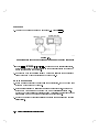
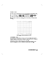
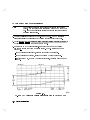
2-1. Measurement Uncertainty Window . . . . . . . . . . . . . .
2-2. Reection Test Port Output Frequency Range and Accuracy Test
Setup . . . . . . . . . . . . . . . . . . . . . . . . . .
2-3. Reection Test Port Output Power Range and Level Linearity Test
Setup . . . . . . . . . . . . . . . . . . . . . . . . . .
2-4. Reection Test Port Output Power Range Test Setup (HP 8752C
Option 004) . . . . . . . . . . . . . . . . . . . . . . .
2-5. Reection Test Port Output Power Level Linearity Test Setup . .
2-6. Transmission Test Port Input Noise Floor Level Test Setup 1 . .
2-7. Transmission Test Port Input Noise Floor Level Test Setup 2 . .
2-8. Transmission Test Port Input Noise Floor Level Test Setup 1 . .
2-9. Transmission Test Port Input Noise Floor Level Test Setup 2 . .
2-10. Transmission Test Port Input Noise Floor Level Test Setup 1 . .
2-11. Transmission Test Port Input Noise Floor Level Test Setup 2 . .
2-12. Test Port Crosstalk Test Setup . . . . . . . . . . . . . . . . .
2-13. Reection Trace Noise Test Setup . . . . . . . . . . . . . . .
2-14. Transmission Trace Noise Test Setup . . . . . . . . . . . . .
2-15. Magnitude Dynamic Accuracy Test Setup . . . . . . . . . . .
2-16. Compression Test Setup . . . . . . . . . . . . . . . . . . .
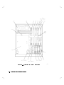
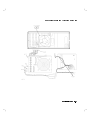
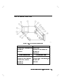
3-1. Location of Major Assemblies . . . . . . . . . . . . . . . . .
3-2. NRM (Normal) and ALT (Alter) Positions of A9 CC Jumper . . .
3-3. Source Adjustment Setup . . . . . . . . . . . . . . . . . . .
3-4. Maximum Intensity Adjustment Set-up . . . . . . . . . . . .
3-5. IF Amplier Correction Constant Setup . . . . . . . . . . . .
3-6. Cavity Oscillator Frequency Correction Constant Setup . . . . .
3-7. Typical Target Spur Using Filter . . . . . . . . . . . . . . .
3-8. Cavity Oscillator Frequency Correction Alternative Setup . . .
3-9. Typical Display of Four Spurs without Filter . . . . . . . . . .
3-10. Typical Display of Five Spurs without Filter . . . . . . . . . .
3-11. Variation of Display of Four Spurs without Filter . . . . . . . .
3-12. Location of Keyword Label . . . . . . . . . . . . . . . . . .
3-13. EEPROM Backup Procedure Setup . . . . . . . . . . . . . .
2-5
2-14
2-16
2-20
2-21
2-25
2-25
2-27
2-27
2-30
2-30
2-33
2-37
2-38
2-42
2-48
3-6
3-7
3-11
3-17
3-19
3-24
3-27
3-28
3-29
3-30
3-31
3-34
3-38
Contents-17
3-14.
3-15.
3-16.
3-17.
3-18.
3-19.
3-20.
3-21.
3-22.
3-23.
3-24.
4-1.
4-2.
4-3.
4-4.
4-5.
4-6.
4-7.
5-1.
5-2.
5-3.
5-4.
5-5.
5-6.
5-7.
5-8.
6-1.
6-2.
6-3.
6-4.
6-5.
6-6.
6-7.
6-8.
7-1.
7-2.
7-3.
7-4.
7-5.
Vertical Position and Focus Adjustment Controls . . . . . . . .
FN VCO TUNE Adjustment Location . . . . . . . . . . . . .
Fractional-N Frequency Range Adjustment Display . . . . . . .
Reection Test Port Output Frequency Accuracy Adjustment
Setup . . . . . . . . . . . . . . . . . . . . . . . . . .
VCXO ADJ Adjustment Location . . . . . . . . . . . . . . .
High/Low Band Transition Adjustment Trace . . . . . . . . .
High/Low Band Adjustments Locations . . . . . . . . . . . .
Fractional-N Spur Avoidance and FM Sideband Adjustment Setup
Location of API and 100 kHz Adjustments . . . . . . . . . . .
A11 Test Point and A3 CAV ADJ Locations . . . . . . . . . .
Display of Acceptable Versus Excessive Spikes . . . . . . . . .
LED Power-up Sequence . . . . . . . . . . . . . . . . . . .
Troubleshooting Organization . . . . . . . . . . . . . . . . .
A15 Preregulator LEDs . . . . . . . . . . . . . . . . . . . .
Front Panel Power-up Sequence . . . . . . . . . . . . . . .
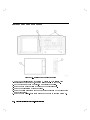
Equipment Setup for Source Power Check . . . . . . . . . . .
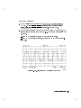
Typical Measurement Trace . . . . . . . . . . . . . . . . .
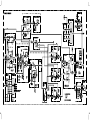
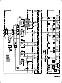
HP 8752C Overall Block Diagram (1 of 4) . . . . . . . . . . .
Power Supply Group Simplied Block Diagram . . . . . . . . .
Location of A15 Diagnostic LEDs . . . . . . . . . . . . . . .
A8 Post Regulator Test Point Locations . . . . . . . . . . . .
Removing the Line Fuse . . . . . . . . . . . . . . . . . . .
Power Supply Cable Locations . . . . . . . . . . . . . . . .
A15W1 Plug Detail . . . . . . . . . . . . . . . . . . . . . .
Front Panel Probe Power Connector Voltages . . . . . . . . .
Power Supply Block Diagram . . . . . . . . . . . . . . . . .
Digital Control Group Block Diagram . . . . . . . . . . . . .
Jumper Positions on the A9 CPU . . . . . . . . . . . . . . .
Location of Four LEDs on A9 CPU . . . . . . . . . . . . . .
Preset Sequence . . . . . . . . . . . . . . . . . . . . . . .
Pin Locations on A19J5 . . . . . . . . . . . . . . . . . . .
Pin Locations on Connector of W14 . . . . . . . . . . . . . .
A9 CPU Walking One Pattern . . . . . . . . . . . . . . . . .
Pin Locations on Connector of W20 . . . . . . . . . . . . . .
Phase Lock Error Troubleshooting Equipment Setup . . . . . .
Jumper Positions on the A9 CPU . . . . . . . . . . . . . . .
Sampler/Mixer to Phase Lock Cable Connection Diagram . . . .
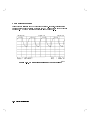
Waveform Integrity in SRC Tune Mode . . . . . . . . . . . .
Phase Locked Output Compared to Open Loop Output in SRC
Tune Mode . . . . . . . . . . . . . . . . . . . . . . . .
Contents-18
3-44
3-47
3-48
3-49
3-50
3-52
3-52
3-55
3-56
3-58
3-59
4-3
4-10
4-11
4-12
4-14
4-15
4-17
5-3
5-4
5-5
5-7
5-9
5-11
5-20
5-25
6-3
6-4
6-5
6-8
6-13
6-14
6-16
6-17
7-4
7-5
7-7
7-9
7-9
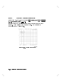
7-6. 1V/GHz at Analog Bus Node 16 with Source PLL O. . . . . .
7-7. YO0 and YO+ Coil Drive Voltage Dierences with SOURCE PLL
OFF . . . . . . . . . . . . . . . . . . . . . . . . . . .
7-8. Sharp 100 kHz Pulses at A13TP5 (any frequency) . . . . . . .
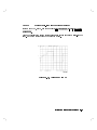
7-9. High Band REF Signal (16 MHz CW) . . . . . . . . . . . . .
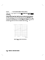
7-10. REF Signal at A11TP9 (5 MHz CW) . . . . . . . . . . . . . .
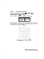
7-11. Typical FN LO Waveform at A12J1 . . . . . . . . . . . . . .
7-12. 4 MHz Reference Signal at A12TP9 (Preset) . . . . . . . . . .
7-13. 90 Degree Phase Oset of High Band 2nd LO Signals (16 MHz
CW) . . . . . . . . . . . . . . . . . . . . . . . . . . .
7-14. In-Phase Low Band 2nd LO Signals (14 MHz CW) . . . . . . . .
7-15. L ENREF Line at A12P2-16 (Preset) . . . . . . . . . . . . . .
7-16. Complementary L HB and L LB Signals (Preset) . . . . . . . .
7-17. 10 MHz HI OUT Waveform from A14J1 . . . . . . . . . . . .
7-18. 25 MHz HI OUT Waveform from A14J1 . . . . . . . . . . . .
7-19. 60 MHz HI OUT Waveform from A14J1 . . . . . . . . . . . .
7-20. LO OUT Waveform at A14J2 . . . . . . . . . . . . . . . . .
7-21. A14 Generated Digital Control Signals . . . . . . . . . . . . .
7-22. H MB Signal at A14P1-5 (Preset and 16 MHz to 31 MHz Sweep) .
7-23. Pulse Generator Output . . . . . . . . . . . . . . . . . . .
7-24. High Quality Comb Tooth at 3 GHz . . . . . . . . . . . . . .
7-25. Stable HI OUT Signal in FRACN TUNE Mode . . . . . . . . . .
7-26. Typical 1st IF Waveform in FRACN TUNE/SRC TUNE Mode . .
7-27. FM Coil { Plot with 3 Point Sweep . . . . . . . . . . . . . .
8-1. Sample R Input Trace . . . . . . . . . . . . . . . . . . . .
8-2. Sample A Input Trace . . . . . . . . . . . . . . . . . . . .
8-3. Sample B Input Trace . . . . . . . . . . . . . . . . . . . .
8-4. 4 MHz REF Waveform . . . . . . . . . . . . . . . . . . . .
8-5. Digital Data Lines Observed Using L INTCOP as Trigger . . . .
8-6. Digital Control Lines Observed Using L INTCOP as Trigger . . .
8-7. 2nd IF (4 kHz) Waveform . . . . . . . . . . . . . . . . . . .
9-1. Typical Return Loss Traces of Good and Poor Cables . . . . . .
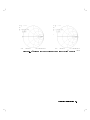
9-2. Typical Smith Chart Traces of Good Short (a) and Open (b) . . .
10-1. Internal Diagnostics Menus . . . . . . . . . . . . . . . . . .
10-2. Jumper Positions on the A9 CPU . . . . . . . . . . . . . . .
10-3. Service Feature Menus . . . . . . . . . . . . . . . . . . . .
10-4. Analog Bus Node 1 . . . . . . . . . . . . . . . . . . . . .
10-5. Analog Bus Node 2 . . . . . . . . . . . . . . . . . . . . .
10-6. Analog Bus Node 3 . . . . . . . . . . . . . . . . . . . . .
10-7. Analog Bus Node 4 . . . . . . . . . . . . . . . . . . . . .
10-8. Analog Bus Node 6 . . . . . . . . . . . . . . . . . . . . .
7-11
7-12
7-16
7-17
7-18
7-19
7-20
7-21
7-22
7-23
7-24
7-26
7-27
7-27
7-28
7-31
7-32
7-33
7-34
7-35
7-36
7-38
8-4
8-5
8-6
8-8
8-10
8-10
8-12
9-5
9-7
10-2
10-9
10-19
10-30
10-31
10-32
10-33
10-34
Contents-19
10-9.
10-10.
10-11.
10-12.
10-13.
10-14.
10-15.
10-16.
10-17.
10-18.
10-19.
11-1.
11-2.
11-3.
11-4.
11-5.
11-6.
11-7.
11-8.
11-9.
12-1.
12-2.
12-3.
12-4.
12-5.
12-6.
12-7.
12-8.
12-9.
13-1.
14-1.
14-2.
14-3.
14-4.
14-5.
14-6.
14-7.
14-8.
14-9.
14-10.
14-11.
Analog Bus Node 7 . . . . . . . . . . . . . . . . . .
Analog Bus Node 14 . . . . . . . . . . . . . . . . . .
Analog Bus Node 15 . . . . . . . . . . . . . . . . . .
Analog Bus Node 16 . . . . . . . . . . . . . . . . . .
Counter Readout Location . . . . . . . . . . . . . . .
Analog Bus Node 18 . . . . . . . . . . . . . . . . . .
Analog Bus Node 20 . . . . . . . . . . . . . . . . . .
Analog Bus Node 23 . . . . . . . . . . . . . . . . . .
Analog Bus Node 29 . . . . . . . . . . . . . . . . . .
Analog Bus Node 30 . . . . . . . . . . . . . . . . . .
Location of Firmware Revision Information on Display . .
Standard Connections for One-Port Error-Correction . . .
Standard Connections for Response Calibration . . . . .
Standard Connections for Isolation Calibration . . . . . .
Typical ED (Reection Test Port) . . . . . . . . . . . .
Typical ES (Reection Test Port) . . . . . . . . . . . .
Typical ER (Reection Test Port) . . . . . . . . . . . .
Typical EX with 10 Hz Bandwidth . . . . . . . . . . .
Typical EX with 3 kHz Bandwidth . . . . . . . . . . .
Typical ET . . . . . . . . . . . . . . . . . . . . . .
Simplied Block Diagram of the Network Analyzer System
Power Supply Functional Group, Simplied Block Diagram
Digital Control Group, Block Diagram . . . . . . . . . .
Low Band Operation of the Source . . . . . . . . . . .
High Band Operation of the Source . . . . . . . . . . .
Receiver Functional Group (standard and Option 003) . .
Receiver Functional Group (Option 003 and 004) . . . . .
Receiver Functional Group (Option 006) . . . . . . . . .
Receiver Functional Group (Option 004 and 006) . . . . .
Module Exchange Procedure . . . . . . . . . . . . . .
Cover Removal Procedure . . . . . . . . . . . . . . .
Initial Front Panel Procedure . . . . . . . . . . . . . .
Location of Screws on Bottom Edge of Frame . . . . . .
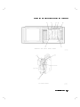
Location of EXT REF cable and GSP Assembly . . . . .
Location of Rear Panel Fasteners . . . . . . . . . . . .
Location of A1 and A2 components . . . . . . . . . . .
Location of Source Parts . . . . . . . . . . . . . . . .
Location of Preregulator Fasteners and Wires . . . . . .
Location of Rear Panel Fasteners . . . . . . . . . . . .
Location of Display Fasteners and Parts . . . . . . . . .
Location of Coupler Screws on Bottom Front Frame . . .
Contents-20
.
.
.
.
.
.
.
.
.
.
.
.
.
.
.
.
.
.
.
.
.
.
.
.
.
.
.
.
.
.
.
.
.
.
.
.
.
.
.
.
.
.
.
.
.
.
.
.
.
.
.
.
.
.
.
.
.
.
.
.
.
.
.
.
.
.
.
.
.
.
.
.
.
.
.
.
.
.
.
.
.
.
.
.
.
.
.
.
.
.
.
.
.
.
.
.
.
.
.
.
.
.
.
.
.
.
.
.
.
.
.
.
.
.
.
.
.
.
.
.
.
.
.
10-35
10-38
10-39
10-40
10-41
10-42
10-43
10-45
10-48
10-49
10-51
11-4
11-6
11-7
11-12
11-14
11-16
11-18
11-18
11-20
12-2
12-6
12-10
12-17
12-21
12-24
12-25
12-26
12-27
13-3
14-3
14-4
14-5
14-6
14-7
14-8
14-10
14-12
14-14
14-16
14-18
14-12. Location of Directional Coupler Hardware . . . . . . . . . . . 14-19
14-13. Location of Fan Wire Bundle and Screws . . . . . . . . . . . 14-20
Contents-21
Tables
1-1.
1-2.
1-3.
5-1.
5-2.
5-3.
5-4.
6-1.
6-2.
6-3.
7-1.
7-2.
7-3.
7-4.
7-5.
7-6.
7-7.
7-8.
8-1.
8-2.
8-3.
9-1.
10-1.
10-2.
11-1.
11-2.
12-1.
12-2.
12-3.
14-1.
Service Test Equipment . . . . . . . . . . . .
Required Tools . . . . . . . . . . . . . . . . .
Connector Care Quick Reference . . . . . . . .
A8 Post Regulator Test Point Voltages . . . . . .
Output Voltages . . . . . . . . . . . . . . . .
Recommended Order for Removal/Disconnection .
Recommended Order for Removal/Disconnection .
LED Code and Pattern Versus Test Failed . . . .
Front Panel Key Codes . . . . . . . . . . . . .
Internal Diagnostic Test with Commentary . . . .
Output Frequency in SRC Tune Mode . . . . . .
Analog Bus Check of Reference Frequencies . . .
A12 Reference Frequencies . . . . . . . . . . .
A12-Related Digital Control Signals . . . . . . .
VCO Range Check Frequencies . . . . . . . . .
A14-to-A13 Digital Control Signal Locations . . .
1st IF Waveform Settings . . . . . . . . . . . .
A11 Input Signals . . . . . . . . . . . . . . .
Signals Required for A10 Assembly Operation . .
2nd IF (4 kHz) Signal Locations . . . . . . . . .
2nd LO Locations . . . . . . . . . . . . . . .
Components Related to Specic Error Terms . . .
Test Status Terms . . . . . . . . . . . . . . .
Descriptions of Jumper Positions . . . . . . . .
Calibration Coecient Terms and Tests . . . . .
Uncorrected System Performance . . . . . . . .
Low Band Subsweep Frequencies . . . . . . . .
High Band Subsweep Frequencies . . . . . . . .
Mixer Frequencies . . . . . . . . . . . . . . .
Post-Repair Procedures . . . . . . . . . . . . .
Contents-22
.
.
.
.
.
.
.
.
.
.
.
.
.
.
.
.
.
.
.
.
.
.
.
.
.
.
.
.
.
.
.
.
.
.
.
.
.
.
.
.
.
.
.
.
.
.
.
.
.
.
.
.
.
.
.
.
.
.
.
.
.
.
.
.
.
.
.
.
.
.
.
.
.
.
.
.
.
.
.
.
.
.
.
.
.
.
.
.
.
.
.
.
.
.
.
.
.
.
.
.
.
.
.
.
.
.
.
.
.
.
.
.
.
.
.
.
.
.
.
.
.
.
.
.
.
.
.
.
.
.
.
.
.
.
.
.
.
.
.
.
.
.
.
.
.
.
.
.
.
.
.
.
.
.
.
.
.
.
.
.
.
.
.
.
.
.
.
.
.
.
.
.
.
.
.
.
.
.
.
.
.
.
.
.
.
.
.
.
.
.
.
.
.
.
.
.
.
.
.
.
.
.
.
.
.
.
.
.
.
.
1-2
1-4
1-6
5-6
5-10
5-12
5-18
6-6
6-9
6-12
7-8
7-13
7-15
7-23
7-25
7-30
7-36
7-38
8-9
8-12
8-13
9-4
10-4
10-8
11-7
11-9
12-18
12-22
12-29
14-22
1
Service Equipment and Analyzer Options
Table of Service Test Equipment
The following tables list the tools and test equipment required to perform the
analyzer's system verication, troubleshooting, adjustment, and performance
tests.
Service Equipment and Analyzer Options
1-1
Table 1-1. Service Test Equipment
Required
Equipment
Spectrum Analyzer
Critical
Specications
Freq. Accuracy 67 Hz
Use*
Recommended
Model
HP 8563E
A, T
Frequency Counter
HP 5343A
P
Measuring Receiver
HP 8902A
P
Oscilloscope
Bandwidth: 100 MHz
Accuracy: 10%
any
T
Digital Voltmeter
Resolution: 10 mV
any
T
Tool Kit
No substitute
HP part number
08753-60023
T
Power Meter (HP-IB)
No substitute
HP 436A Opt. 022,
HP 437A or 438A
A, P, T
Power Sensor
Frequency: 300 kHz-3 GHz, 50
HP 8482A
A, P, T
Power Sensor (for Option 006)
Frequency: 3 GHz-6 GHz
HP 8481A Opt 006
A, P, T
Power Sensor
Frequency: 300 kHz-3 GHz, 75
HP 8483A Opt. H03
P
Photometer
Tektronix J16
A
Photometer Probe
Tektronix J6503
A
Light Occluder
Tektronix
016-0305-00
A
CRT Demagnetizer or Bulk Tape
Eraser
A
Printer
HP ThinkJet,
DeskJet, LaserJet
P
Disk Drive
3.5-inch
HP 9122
Floppy Disk
3.5-inch
HP 92192A
A
Calibration Kit Type-N, 50
No substitute
HP 85032B
P
Calibration Kit Type-N, 75
No substitute
HP 85036B
P
Verication Kit 7 mm
No substitute
HP 85029B
P
Low Pass Filter
>50 dB @ 2.96 Hz and passband that
HP P/N 9135-0198
A
includes 800 MHz
Step Attenuator
110 dB
Attenuators (xed):
Return loss:
HP 8496A
P
HP 8491A Opt. 020
P, T
Power Splitter
2-Way, 50
HP 11667A
P, T
Minimum Loss Pad
Type-N, 50
to 75
HP 11852B
P, T
32 dB APC-7 20 dB (2)
1-2 Service Equipment and Analyzer Options
Table 1-2. Service Test Equipment (2 of 2)
Required
Equipment
Critical
Specications
Use*
Recommended
Model
Adapter
BNC to Alligator Clip
HP P/N 8120-1292
A
Adapter
APC-3.5 (m) to type-N (f)
HP P/N 1250-1750
A, P
Adapter
APC-3.5 (f) to type-N (f)
HP P/N 1250-1745
A, P
Adapter
APC-3.5 (f) to type-N (m)
HP P/N 1250-1744
A
Adapter
BNC (m) to type-N (f)
HP P/N 1250-0077
P
Adapter
type-N (m) to type-N (m)
HP P/N 1250-1528
P
RF Cable
24-inch, type-N, 75
HP P/N 8120-2408
A, P
RF Cable
24-inch, type-N, 50
HP P/N 8120-4781
A, P
RF Cable Set
type-N, 50
HP 11851B
P
HP 10833A/B/C/D
A
HP-IB Cable
Coax Cable
BNC
HP P/N 8120-1840
A
Coax Cable
BNC (m) to BNC (m), 50
HP 10503A
A
Antistatic Wrist Strap
HP P/N 9300-1367
A, T, P
Antistatic Wrist Strap Cord
HP P/N 9300-0980
A, T, P
Static-control Table Mat and
Earth Ground Wire
HP P/N 9300-0797
A, T, P
* P - Performance Tests
A - Adjustment
T - Troubleshooting
Service Equipment and Analyzer Options
1-3
Table 1-2. Required Tools
T-8, T-10 and T-15 TORX screwdrivers
Flat-blade screwdrivers|small, medium, and large
5/16-inch open-end wrench (for SMA nuts)
3/16, 5/16, and 9/16-inch hex nut drivers
5/16-inch open-end torque wrench (set to 10 in-lb)
2.5-mm hex-key driver
Non-conductive and non-ferrous adjustment tool
Needle-nose pliers
Tweezers
Antistatic work mat with wrist-strap
1-4 Service Equipment and Analyzer Options
Principles of Microwave Connector Care
Proper connector care and connection techniques are critical for accurate,
repeatable measurements.
Refer to the calibration kit documentation for connector care information.
Prior to making connections to the network analyzer, carefully review the
information about inspecting, cleaning and gaging connectors.
Having good connector care and connection techniques extends the life of these
devices. In addition, you obtain the most accurate measurements.
This type of information is typically located in Chapter 3 of the calibration kit
manuals.
For additional connector care instruction, contact your local Hewlett-Packard
Sales and Service Oce about course numbers HP 85050A+24A and
HP 85050A+24D.
See the following table for quick reference tips about connector care.
Service Equipment and Analyzer Options
1-5
Table 1-3. Connector Care Quick Reference
Do
Handling and Storage
Keep connectors clean
Extend sleeve or connector nut
Use plastic end-caps during storage
Do
Do Not
Touch mating-plane surfaces
Set connectors contact|end down
Visual Inspection
Do Not
Inspect all connectors carefully
Use a damaged connector|ever
Look for metal particles, scratches, and dents
Do
Connector Cleaning
Try compressed air rst
Use isopropyl alcohol
Clean connector threads
Do
Gaging Connectors
Clean and zero the gage before use
Use the correct gage type
Use correct end of calibration block
Gage all connectors before rst use
Do
Do Not
Use any abrasives
Get liquid into plastic support beads
Making Connections
Align connectors carefully
Make preliminary connection lightly
Turn only the connector nut
Use a torque wrench for nal connect
1-6 Service Equipment and Analyzer Options
Do Not
Use an out-of-spec connector
Do Not
Apply bending force to connection
Over tighten preliminary connection
Twist or screw any connection
Tighten past torque wrench \break" point
Analyzer Options Available
Option 003, 3 GHz Operation
This option extends the maximum source and receiver frequency of the analyzer
to 3 GHz.
Option 004, Step Attenuator
This option provides a source output power range from 085 to +10 dBm.
Option 006, 6 GHz Operation
This option extends the maximum source and receiver frequency of the analyzer
to 6 GHz.
Option 010, Time Domain
This option displays the time domain response of a network by computing
the inverse Fourier transform of the frequency domain response. It shows
the response of a test device as a function of time or distance. Displaying the
reection coecient of a network versus time determines the magnitude and
location of each discontinuity. Displaying the transmission coecient of a
network versus time determines the characteristics of individual transmission
paths. Time domain operation retains all accuracy inherent with the correction
that is active in such devices as SAW lters, SAW delay lines, RF cables, and RF
antennas.
Option 075, 75
Impedance
This option oers 75
impedance bridges with type-N test port connectors.
Option 1CM, Rack Mount Flange Kit Without Handles
This option is a rack mount kit containing a pair of anges and the necessary
hardware to mount the instrument, with handles detached, in an equipment
rack with 482.6 mm (19 inches) horizontal spacing.
Service Equipment and Analyzer Options
1-7
Option 1CP, Rack Mount Flange Kit With Handles
This option is a rack mount kit containing a pair of anges and the necessary
hardware to mount the instrument with handles attached in an equipment rack
with 482.6 mm (19 inches) spacing.
Option AFN, add 50
Test Port Cable
This option provides a second type-N male to type-N male test port cable and a
type-N female to type-N female adapter. Instructions are included for storing a
new internal calibration to account for the eects of this cable.
Option AFP, add 75
Test Port Cable
This option provides a 75
type-N male to type-N female test port cable.
Instructions are included for storing a new internal calibration to account for
the eects of this cable.
Option B02, External Disk Drive
This option provides an external disk drive and an HP-IB cable.
1-8 Service Equipment and Analyzer Options
Service and Support Options
Hewlett-Packards oers many repair and calibration options for your analyzer.
Contact the nearest Hewlett-Packard sales or service oce for information on
options available for your analyzer. See the table titled \Hewlett-Packard Sales
and Service Oces" in Chapter 15.
Service Equipment and Analyzer Options
1-9
System Verication and Performance
Tests
2
How to Test the Performance of Your Analyzer
To obtain the same quality of performance testing that Hewlett-Packard has
administered at the factory, you must perform:
the system verication procedure
AND
all of the performance test procedures.
This quality of performance testing guarantees that the analyzer is performing
within all of the published specications. A Hewlett-Packard Customer Engineer
will issue a Certicate of Calibration for your analyzer if two conditions are
met:
Your analyzer passes all the performed tests.
The equipment and standards that were used to perform the tests are
traceable to a national standards institute.
Note
If you have a particular type of measurement application that
does not use all of the analyzer's measurement capabilities,
you may ask your local Hewlett-Packard Customer Service
Center for a subset of specications that you want veried.
However, this does create the potential for making incorrect
measurements when using a dierent application.
System Verication and Performance Tests 2-1
Sections in this Chapter
HP 8752C System Verication
HP 8752C Performance Tests
1. Reection Test Port Output Frequency Range and Accuracy
2. Reection Test Port Output Power Range and Level Linearity (HP 8752C
without Option 004)
3. Reection Test Port Output Power Range and Level Linearity (HP 8752C
with Option 004)
4. Transmission Test Port Input Noise Floor Level (HP 8752C without
Option 075)
5. Transmission Test Port Input Noise Floor Level (HP 8752C with
Option 075)
6. Test Port Crosstalk
7. System Trace Noise
8. Magnitude Dynamic Accuracy (HP 8752C 0 All Options)
9. Phase Dynamic Accuracy (HP 8752C 0 All Options)
10. Compression
HP 8752C Performance Test Record
2-2 System Verication and Performance Tests
HP 8752C System Verication
Equipment
For standard HP 8752C network analyzer:
Calibration kit (50
, type-N) : : : : : : : : : : : : : : : : : : : : : : : : : : : : : : : : : : : : : : : : : : HP 85032B
Cable type-N (50
) 24-inch : : : : : : : : : : : : : : : : : : : : : : : : : : : : : : : : : : : : HP P/N 8120-4781
Printer : : : : : : : : : : : : : : : : : : : : : : : : : : : : : : : : : : : : : : : : : : HP ThinkJet, DeskJet, LaserJet
For the HP 8752C with Option 075:
Calibration kit (75
, type-N) : : : : : : : : : : : : : : : : : : : : : : : : : : : : : : : : : : : : : : : : : : HP 85036B
Cable type-N (75
) 24-inch : : : : : : : : : : : : : : : : : : : : : : : : : : : : : : : : : : : : HP P/N 8120-2408
Printer : : : : : : : : : : : : : : : : : : : : : : : : : : : : : : : : : : : : : : : : : : HP ThinkJet, DeskJet, LaserJet
Warm-up time: one hour.
Description
The HP 8752C system verication consists of performing the verication
procedure mentioned in this section. The verication procedure is
semi-automated and controlled by the analyzer's rmware.
The verication procedure involves measuring a set of calibration devices
(supplied in the HP 85032B 50
type-N calibration kit or the HP 85036B 75
type-N calibration kit) and comparing the measured data to the specication
limits drawn on the analyzer display. The measured data must fall within the
specication limits at all frequencies to pass the test.
System verication is only part of an instrument's calibration procedure.
The complete set of instrument specications can be tested by performing
the \HP 8752C System Verication" and all of the analyzer's performance
tests. An HP 85032B Option 002 or an HP 85036B Option 1BP calibration kit
(including with a Certicate of Calibration with United States National Institute
of Standards and Technology (NIST) test numbers) is required for a calibration
traceable to NIST.
Note
A Certicate of Calibration is issued if the analyzer's system
verication as well as all of the performance tests are
performed by a Hewlett-Packard Customer Engineer with all
having passed.
System Verication and Performance Tests 2-3
System Verication Cycle and Kit Recertication
The recommended system verication cycle is every six months. HewlettPackard also suggests the calibration kit be recertied annually. For more
information about the kit recertication, refer to the HP 85032B 50
Type-N
Calibration Kit Operation and Service Manual or HP 85036B 75
Type-N
Calibration Kit Operation and Service Manual.
Measurement Uncertainty
Associated with any analyzer are measurement errors that add uncertainty to
the measured results. This uncertainty limits how accurately a device under test
(DUT) can be measured.
The measurement uncertainty is dened to be the sum of the residual
systematic (repeatable) and random (non-repeatable) errors in the measurement
system. The systematic errors are eective directivity, eective source match,
load match, reection and transmission tracking, and isolation (crosstalk).
Random errors include errors due to noise, drift, connector repeatability, and
test cable stability.
The typical measurement uncertainties for type-N connectors using a
1-port error correction utilize an RSS (Root Sum of Squares) model for the
contributions of random errors such as noise, pin depth, pin diameter variation,
load return loss, and connector repeatability.
Measurement Uncertainty Window
The PASS/FAIL result of the limit line test generally indicates the status of the
verication test. The validity of the limit lines, drawn on the analyzer display
during the verication tests, are determined by the measurement uncertainty.
The measurement uncertainty must be taken into account when analyzing
the test results. If the analyzer detects the test data outside of the limits, a
FAIL will be displayed on the analyzer. This FAIL status may not represent
a true failure if at the worst point, the test data is within the measurement
uncertainty window (not displayed on the analyzer). Refer to Figure 2-1 for
interpretations of test data.
2-4 System Verication and Performance Tests
Figure 2-1. Measurement Uncertainty Window
System Verication and Performance Tests 2-5
HP 8752C Type-N Test Port Characteristics (50
System)
Directivity
Frequency Range
Specication
Measurement Uncertainty
300 kHz to 1.3 GHz
40 dB1
1.3 GHz to 3.0 GHz
35 dB
3.0 GHz to 6.0 GHz
30 dB
63.30 dB
62.51 dB
63.30 dB
Specication
Measurement Uncertainty
300 kHz to 1.3 GHz
30 dB
1.3 GHz to 3.0 GHz
25 dB
3.0 GHz to 6.0 GHz
20 dB
62.51 dB
62.88 dB
62.88 dB
Specication
Measurement Uncertainty
300 kHz to 1.3 GHz
23 dB
1.3 GHz to 3.0 GHz
20 dB
3.0 GHz to 6.0 GHz
16 dB
62.51 dB
62.88 dB
62.88 dB
1
30 dB, 300 kHz to 10 MHz
Source Match (Reection)
Frequency Range
Source Match (Transmission)*
Frequency Range
*Option 004 may degrade transmission source match as much as 2 dB, resulting in up to 0.05 dB additional
uncertainty in transmission tracking.
Reection Tracking
Frequency Range
300 kHz to 1.3 GHz
1.3 GHz to 3.0 GHz
3.0 GHz to 6.0 GHz
Specication
Measurement Uncertainty
60.2 dB
60.3 dB
60.4 dB
60.009 dB
60.019 dB
60.070 dB
2-6 System Verication and Performance Tests
Load Match
Frequency Range
Specication
Measurement Uncertainty
300 kHz to 1.3 GHz
23 dB1
1.3 GHz to 3.0 GHz
20 dB
3.0 GHz to 6.0 GHz
18 dB
60.40 dB
60.40 dB
60.92 dB
1
14 dB, 300 kHz to 10 MHz for analyzers with option 006
Transmission Tracking
Frequency Range
300 kHz to 1.3 GHz
1.3 GHz to 3.0 GHz
3.0 GHz to 6.0 GHz
Specication
Measurement Uncertainty
60.2 dB
60.3 dB
60.5 dB
60.043 dB
60.086 dB
60.172 dB
HP 8752C Type-N Test Port Characteristics (75
System)
Directivity
Frequency Range
Specication
Measurement Uncertainty
300 kHz to 10 MHz
30 dB
10 MHz to 1.3 GHz
40 dB
1.3 GHz to 3.0 GHz
35 dB
64.41 dB
64.41 dB
64.41 dB
Specication
Measurement Uncertainty
300 kHz to 1.3 GHz
30 dB
1.3 GHz to 3.0 GHz
25 dB
62.88 dB
63.30 dB
Source Match (Reection)
Frequency Range
System Verication and Performance Tests 2-7
Source Match (Transmission)*
Frequency Range
Specication
Measurement Uncertainty
300 kHz to 1.3 GHz
23 dB
1.3 GHz to 3.0 GHz
20 dB
62.88 dB
63.30 dB
*Option 004 may degrade transmission source match as much as 2 dB, resulting in up to 0.05 dB additional
uncertainty in transmission tracking.
Reection Tracking
Frequency Range
Specication
Measurement Uncertainty
60.2 dB
60.3 dB
60.2 dB
60.3 dB
Specication
Measurement Uncertainty
300 kHz to 1.3 GHz
23 dB
1.3 GHz to 3.0 GHz
20 dB
60.50 dB
60.64 dB
Specication
Measurement Uncertainty
60.2 dB
60.3 dB
60.20 dB
60.30 dB
300 kHz to 1.3 GHz
1.3 GHz to 3.0 GHz
Load Match
Frequency Range
Transmission Tracking
Frequency Range
300 kHz to 1.3 GHz
1.3 GHz to 3.0 GHz
2-8 System Verication and Performance Tests
System Verication Procedure
1. Switch the analyzer's line power ON. Press 4
5.
2. If you want a printout of the verication data, press 4
5
SYSTEM CONTROLLER 4
5 SERVICE MENU TEST OPTIONS RECORD ON .
Otherwise, go to the next step.
PRESET
LOCAL
NNNNNNNNNNNNNNNNNNNNNNNNNNNNNNNNNNNNNNNNNNNNNNNNNNNNN
NNNNNNNNNNNNNNNNNNNNNNNNNNNNNNNNNNNNNN NNNNNNNNNNNNNNNNNNNNNNNNNNNNNNNNNNNNNN NNNNNNNNNNNNNNNNNNNNNNNNNNNNN
SYSTEM
Note
Once you have activated the record function, you cannot switch
it OFF during the verication procedure. Be sure the paper in
the printer is setup so that printing starts at the top of the page.
In case of printer diculty:
If you have an HP-IB compatible printer, verify that the printer
address is set to 1.
Refer to the HP 8752C Network Analyzer User's Guide for more
information on how to perform this task.
NNNNNNNNNNNNNNNNNNNNNNNNNNNNNNNNNNNNNN NNNNNNNNNNNNNNNNN NNNNNNNNNNNNNNNNNNNNNNNNNNNNNNNNNNNNNNNNN NNNNNNNNNNNNNNNNNNNNNNNNNNNNNNNNNNNNNN
3. Press 4
5 SERVICE MENU TESTS SYS VER TESTS EXECUTE TEST . A
brief description of the test procedure is shown on the analyzer display. To
begin the test, press CONTINUE .
SYSTEM
NNNNNNNNNNNNNNNNNNNNNNNNNN
4. Connect a type-N male open to the analyzer's reection test port. Press
CONTINUE .
NNNNNNNNNNNNNNNNNNNNNNNNNN
5. When the measurement is done, connect a type-N male short to the reection
test port. Press CONTINUE .
NNNNNNNNNNNNNNNNNNNNNNNNNN
6. At the prompt, connect a type-N load to the reection test port. Press
CONTINUE . After measuring the load, the system directivity is checked and
the test result is displayed on the analyzer.
NNNNNNNNNNNNNNNNNNNNNNNNNN
Note
NNNNNNNNNNNNNNNNNNNNNNNNNNNNN
If you have not activated the RECORD ON feature, you need to
press CONTINUE after EACH of the following tests:
NNNNNNNNNNNNNNNNNNNNNNNNNN
a. Source Match (Reection Mode)
b. Source Match (Transmission Mode)
c. Reection Tracking
System Verication and Performance Tests 2-9
7. Connect a type-N RF cable between the analyzer's reection and
transmission test ports. Press CONTINUE to test the system load match.
NNNNNNNNNNNNNNNNNNNNNNNNNN
8. If you have activated the record feature, the system will automatically test
its transmission tracking. Otherwise, press CONTINUE to access this test.
NNNNNNNNNNNNNNNNNNNNNNNNNN
9. Press CONTINUE to end the system verication procedure.
NNNNNNNNNNNNNNNNNNNNNNNNNN
In case of diculty
1. Refer to the \Adjustments and Correction Constants" chapter of this manual.
Perform the \Frequency Response Correction Constants Adjustment"
procedure. Repeat the \HP 8752C System Verication" procedure.
2-10 System Verication and Performance Tests
HP 8752C Performance Tests
This portion of the manual contains performance tests which are part of the
instrument calibration process. An instrument calibration includes the system
verication, described in the previous section, and the performance tests.
To test the complete set of instrument specications, both portions of the
instrument calibration must be performed.
Note
Before performing these performance tests, check that the test
equipment is operating to specication. Gage and clean all
connectors.
The following is a list of performance tests in the order in which they should be
performed:
1. Reection Test Port Output Frequency Range and Accuracy
2. Reection Test Port Output Power Range and Level Linearity (For HP 8752C
Analyzers without Option 004)
3. Reection Test Port Output Power Range and Level Linearity (For HP 8752C
Analyzers with Option 004)
4. Transmission Test Port Input Noise Floor Level (For HP 8752C Analyzers
without Option 075)
5. Transmission Test Port Input Noise Floor Level (For HP 8752C Analyzers
with Option 075)
6. Test Port Crosstalk
7. System Trace Noise
8. Magnitude Dynamic Accuracy
9. Phase Dynamic Accuracy
10. Compression
Note
Unless otherwise specied, the performance tests are applicable
to a standard HP 8752C or an HP 8752C with options.
System Verication and Performance Tests 2-11
Equipment Required to Run the Performance Tests
Description
Quantity
HP Model or Part Number
Calibration kit, 50
type-N
1
HP 85032B
Calibration kit, 75
type-N
1
HP 85036B
Measuring Receiver
1
HP 8902A
Frequency counter
1
HP 5343A
Power meter
1
HP 436A, HP 437A, HP 438A
Power sensor
1
HP 8482A
Power sensor
1
HP 8481A
Power sensor
1
HP 8483A
Power sensor
1
HP 8483A Option H03
Printer
1
HP ThinkJet, DeskJet,
LaserJet
110 dB step attenuator
1
HP 8496A
2-Way power splitter, 50
1
HP 11667A
Cable, 50
type-N 24-inch
3
HP P/N 8120-4781
Cable, 75
type-N 24-inch
2
HP P/N 8120-2408
Minimum Loss Pad
2
HP 11852B
Adapter type-N(m) to type-N(m)
1
HP P/M 1250-1528
Adapter BNC(m) to N(f)
1
HP P/N 1250-0077
Adapter APC-3.5mm(f) to N(f)
1
HP P/N 1250-1745
1
2
1
3
1
1
Required only for instruments with Option 075
Required only for instruments with Option 006
3 Required only for instruments with Option 003 and Option 075
1
2
2-12 System Verication and Performance Tests
1. Reection Test Port Output Frequency Range and
Accuracy
Specications
Frequency Range
300 kHz to 1.3 GH
300 kHz to 3 GHz
2
300 kHz to 6 GHz3
Frequency Accuracy1
610 ppm
610 ppm
610 ppm
At 25 C 6 5 C
2 HP 8752C with Option 003
3 HP 8752C with Option 006
1
Equipment
Frequency counter : : : : : : : : : : : : : : : : : : : : : : : : : : : : : : : : : : : : : : : : : : : : : : : : : : : : : HP 5343A
Adapter BNC(m) to N(f) : : : : : : : : : : : : : : : : : : : : : : : : : : : : : : : : : : : : : : : HP P/N 1250-0077
Adapter APC-3.5(f) to N(f) : : : : : : : : : : : : : : : : : : : : : : : : : : : : : : : : : : : : HP P/N 1250-1745
Cable (50
, type-N) 24-inch : : : : : : : : : : : : : : : : : : : : : : : : : : : : : : : : : : : HP P/N 8120-4781
Additional equipment required for analyzers with Option 075
50
to 75
minimum loss pad : : : : : : : : : : : : : : : : : : : : : : : : : : : : : : : : : : : : : : : : HP 11852B
Warm-up time: 30 minutes.
Description
This test determines the analyzer's reection test port output frequency range
and accuracy over its entire operating frequency range. The frequencies are
veried relative to room temperature (25 C, 65 C).
System Verication and Performance Tests 2-13
Procedure
1. Connect the equipment as shown in Figure 2-2. Press 4
5.
PRESET
Figure 2-2.
Reection Test Port Output Frequency Range and Accuracy Test Setup
2. Press 4
5 CW FREQ 4 5 4 5 4 5 4
5. Depending on the analyzer's options,
record the frequency counter reading in the appropriate table (2 through 6)
in the \Performance Test Record."
3. Repeat step 2 for each instrument's CW frequency listed in the appropriate
table (2 through 6) in the \Performance Test Record."
NNNNNNNNNNNNNNNNNNNNNNN
MENU
3
0
0
k/m
In case of diculty
1. If any measured frequency barely fails the specication, check the time base
accuracy of the frequency counter.
2. If the analyzer fails by a signicant margin at all frequencies, perform the
\Frequency Accuracy" and the \High/Low Band Transition" adjustments.
Refer to the chapter titled \Adjustments and Correction Constants" for more
information on how to perform these adjustment procedures.
3. Refer to the \Source Troubleshooting" chapter in this manual if the problem
still persists.
2-14 System Verication and Performance Tests
2. Reection Test Port Output Power Range and Level
Linearity (For HP 8752C Analyzers without
Option 004)
Specications
Power Range
020 to 015 dBm
015 to 0 dBm
0 to +5 dBm
Power Level Linearity Relative to 05 dBm
60.5 dB
60.2 dB
60.5 dB
Equipment
For standard analyzers:
Power meter : : : : : : : : : : : : : : : : : : : : : : : : : : : : : : : : : : : : : : : : : : : : : : : : HP 436A/437B/438A
Power sensor : : : : : : : : : : : : : : : : : : : : : : : : : : : : : : : : : : : : : : : : : : : : : : : : : : : : : : : : : : : HP 8482A
Additional equipment required for analyzers with Option 006
Power sensor : : : : : : : : : : : : : : : : : : : : : : : : : : : : : : : : : : : : : : : : : : : : : : : : : : : : : : : : : : : HP 8481A
Equipment required for analyzers with Option 075
Power meter : : : : : : : : : : : : : : : : : : : : : : : : : : : : : : : : : : : : : : : : : : : : : : : : HP 436A/437B/438A
Power sensor : : : : : : : : : : : : : : : : : : : : : : : : : : : : : : : : : : : : : : : : : : : : : : : : : : : : : : : : : : : HP 8483A
Warm-up time: 30 minutes.
Description
This test determines the reection test port output power range and level
linearity for all analyzers without Option 004. The specications are veried
by rst setting a reference at 05 dBm for relative power measurements. Next,
the analyzer's reection test port output power is stepped and measured over
its operating power range. The power level linearity is found by calculating the
dierence between the power meter reading and the power oset listed in the
appropriate table (7 through 13) of the \Performance Test Record."
System Verication and Performance Tests 2-15
Procedure
Power Range and Level Linearity for an HP 8752C or an HP 8752C
Option 075
1. Connect the equipment as shown in Figure 2-3.
Note
For instruments with Option 075:
a. use an HP 8483A (75
) power sensor
b. use tables 11 through 13 in the \Performance Test Record."
For instruments with Option 075 and Option 003, use an
HP 8483A Option H03 (75
) power sensor.
Figure 2-3.
Reection Test Port Output Power Range and Level Linearity Test Setup
2. Zero and calibrate the power meter. For more information on how to
perform this task, refer to the power meter Operating and Service manual.
3. Press 4
5 4
5 CW FREQ 4 5 4 5 4 5 4
5.
NNNNNNNNNNNNNNNNNNNNNNN
PRESET
MENU
3
0
0
k/m
4. Press POWER 405 4 5 4 5. Set the power meter cal factor for this CW
frequency. On the power meter, set the current power level as the
reference for relative power (dB) measurements. This can be done by
NNNNNNNNNNNNNNNNN
5
x1
2-16 System Verication and Performance Tests
pressing 4
panel.
5
dB REF
on an HP 436A or 4
5
REL
on an HP 438A power meter front
5. Press POWER 405 4 5 4 5 4 5. Record the power meter reading in the \Results
Measured" column on the \Performance Test Record."
6. Utilizing the Power Oset value listed in the \Performance Test Record,"
calculate the test port output power level linearity using the following
formula:
Power Level Linearity = Measured Value + Power Oset
7. Record the result of your calculation on the \Performance Test Record."
8. Repeat steps 5, 6, and 7 for the other power levels listed in the \HP 8752C
Performance Test Record (7 of 28)."
9. Press 4
5 CW FREQ 4 5 4 5 4 5 4
5.
NNNNNNNNNNNNNNNNN
2
0
x1
NNNNNNNNNNNNNNNNNNNNNNN
MENU
1
.
3
G/n
10. Press POWER 405 4 5 4 5. Set the power meter cal factor for this CW
frequency. Press the appropriate hardkey (4
5 or 4
5) on the
HP 436A/438A power meter front panel for relative power measurements.
11. Repeat steps 5, 6, and 7 for the other power levels listed in the \HP 8752C
Performance Test Record (8 of 28)."
12. This completes the \Reection Test Port Output Power Range and Level
Linearity" test if you are working with either a standard analyzer or an
analyzer with only Option 075. Otherwise, go to the appropriate section
below to continue the reection test port performance tests for other
options.
NNNNNNNNNNNNNNNNN
5
x1
dB REF
REL
Power Range and Level Linearity for an HP 8752C with Option 003
13. Press 4
5
MENU
NNNNNNNNNNNNNNNNNNNNNNN
CW FREQ
435 4G/n5.
14. Press POWER 405 4 5 4 5. Set the power meter cal factor for this CW
frequency. Press the appropriate softkey (4
5 or 4
5) on the power
meter front panel for relative power measurements.
15. Press POWER 405 4 5 4 5 4 5. Record the power meter reading in the
\Measured Value" column on the \HP 8752C Performance Test Record
(9 of 28)."
NNNNNNNNNNNNNNNNN
5
x1
dB REF
REL
NNNNNNNNNNNNNNNNN
2
0
x1
System Verication and Performance Tests 2-17
16. Utilizing the Power Oset value listed in the \Performance Test Record
(9 of 28)," calculate the Power Level Linearity using the following formula:
Power Level Linearity = Measured Value + Power Oset
17. Record the result of your calculation on the \Performance Test Record
(9 of 28)."
18. Repeat steps 15, 16, and 17 for the other power levels listed in the
\Performance Test Record (9 of 28)."
Power Range and Level Linearity for an HP 8752C with Options 003
and 075
19. Press 4
5
MENU
NNNNNNNNNNNNNNNNNNNNNNN
CW FREQ
425 4G/n5.
20. Perform steps 14, 15, 16, and 17 for the power levels listed in the
\Performance Test Record (12 of 28)."
Power Range and Level Linearity for an HP 8752C with Option 006
21. Press 4
5
MENU
NNNNNNNNNNNNNNNNNNNNNNN
CW FREQ
465 4G/n5.
22. Perform steps 14, 15, 16, 17, and 18 for the power levels listed in the
\Performance Test Record (10 of 28)."
In case of diculty
1. If you cannot set the test port power at any power level, be sure the
analyzer's source power is activated. To do so, press 4
5 POWER . Check
the SOURCE PWR softkey. ON should be highlighted.
NNNNNNNNNNNNNNNNN
MENU
NNNNNNNNNNNNNNNNNNNNNNNNNNNNNNNN
2. Refer to the \Adjustments and Correction Constants" chapter in this manual.
Perform the \RF Output Power Correction Constants Adjustment" procedure.
3. If the problem still exists, refer to the \Source Troubleshooting" chapter in
this manual for more troubleshooting information.
2-18 System Verication and Performance Tests
3. Reection Test Port Output Power Range and Level
Linearity (HP 8752C with Option 004)
Specications
HP 8752C Option
Power Range
Option 004
085 to +10 dBm
Options 004 and 075
085 to +8 dBm
1
Power Level Linearity1
60.2 dB (015 to +5 dBm)
60.5 dB (+5 to +10 dBm)
60.2 dB (015 to +5 dBm)
60.5 dB (+5 to +8 dBm)
Relative to 05 dBm
Equipment
For standard analyzers:
Power meter : : : : : : : : : : : : : : : : : : : : : : : : : : : : : : : : : : : : : : : : : : : : : : : : : HP436A/437B/438A
Power sensor : : : : : : : : : : : : : : : : : : : : : : : : : : : : : : : : : : : : : : : : : : : : : : : : : : : : : : : : : : : HP 8482A
Cable (50
, type-N) 24-inch : : : : : : : : : : : : : : : : : : : : : : : : : : : : : : : : : : : HP P/N 1250-1745
Additional equipment required for analyzers with Option 006
Power sensor : : : : : : : : : : : : : : : : : : : : : : : : : : : : : : : : : : : : : : : : : : : : : : : : : : : : : : : : : : : HP 8481A
Equipment required for analyzers with Option 075
Power meter : : : : : : : : : : : : : : : : : : : : : : : : : : : : : : : : : : : : : : : : : : : : : : : : : HP436A/437B/438A
Power sensor : : : : : : : : : : : : : : : : : : : : : : : : : : : : : : : : : : : : : : : : : : : : : : : : : : : : : : : : : : : HP 8483A
Cable (75
, type-N) 24-inch : : : : : : : : : : : : : : : : : : : : : : : : : : : : : : : : : : : HP P/N 8120-2408
Warm-up time: 30 minutes.
Description
This test determines the reection test port output power range and level
linearity for an analyzer with Option 004. To verify the analyzer power ranges,
a power level of 010 dBm is rst selected and normalized. Next, various
power levels in dierent power ranges are selected and compared to the
specications listed in the \Performance Test Record." The analyzer power level
linearity is conrmed by rst setting a reference (at 05 dBm) for relative power
measurements. Next, the analyzer's reection test port output power is stepped
System Verication and Performance Tests 2-19
and measured over its specied power range. The power level linearity is found
by calculating the dierence between the power meter reading and the power
oset listed in the \Performance Test Record."
Procedure
Power Range for an HP 8752C with Option 004
1. Connect the equipment as shown in Figure 2-4.
Figure 2-4.
Reection Test Port Output Power Range Test Setup
(HP 8752C Option 004)
2. Press 4
5 4CH 25
PRESET
to set the analyzer up for transmission measurements.
3. Press 4
5 POWER PWR RANGE MAN POWER RANGES
RANGE 0 015 to +10 . Enter the power level value listed in the
the \Performance Test Record (14 of 28)." For this power range, press 405 4 5
4 5 4 5.
4. Press 4
5 DATA!MEMORY DATA/MEM 4
5 SCALE/DIV 4 5 4 5 4 5 to
normalize and scale down the data trace.
5. To activate the analyzer's statistic feature, press 4
5
MARKER MODE MENU STATS ON .
NNNNNNNNNNNNNNNNN NNNNNNNNNNNNNNNNNNNNNNNNNNNNNNNNNNNNNNNNN NNNNNNNNNNNNNNNNNNNNNNNNNNNNNNNNNNNNNN
MENU
NNNNNNNNNNNNNNNNNNNNNNNNNNNNNNNNNNNNNNNNNNNNNNNNNNNNNNNNNNNN
1
0
x1
NNNNNNNNNNNNNNNNNNNNNNNNNNNNNNNNNNNNN NNNNNNNNNNNNNNNNNNNNNNNNNN
DISPLAY
NNNNNNNNNNNNNNNNNNNNNNNNNNNNN
SCALE REF
MKR FCTN
NNNNNNNNNNNNNNNNNNNNNNNNNNNNNNNNNNNNNNNNNNNNNNNNNN NNNNNNNNNNNNNNNNNNNNNNNNNN
6. Press 4
5
MENU
NNNNNNNNNNNNNNNNNNNNNNNNNNNNNNNNNNNNNN NNNNNNNNNNNNNNNNNNNNNNNNNNNNNNNNNNNNNNNNNNNNNNNNNN
TRIGGER MENU NUMBER of GROUPS
2-20 System Verication and Performance Tests
455 4x15.
.
5
x1
7. When the analyzer nishes the sweeps, record the data trace mean value
(as shown on the upper right-hand corner of the analyzer display) on the
\Performance Test Record (14 of 28)."
8. Press 4
5 POWER POWER RANGES RANGE 1 025 to 0 . Enter the power
level value listed in the \Performance Test Record." For this power range,
press 405 4 5 4 5 4 5.
9. Repeat steps 6, 7 and 8 for the other power ranges listed in the \Performance
Test Record (14 of 28)."
NNNNNNNNNNNNNNNNN NNNNNNNNNNNNNNNNNNNNNNNNNNNNNNNNNNNNNN NNNNNNNNNNNNNNNNNNNNNNNNNNNNNNNNNNNNNNNNNNNNNNNNNNN
MENU
2
0
x1
Power Level Linearity for an HP 8752C with Option 004
or an HP 8752C withOptions 004 and 075
1. Connect the equipment as shown in Figure 2-5.
Note
For instruments with Option 075:
a. use an HP 8483A (75
) power sensor
b. use tables 19 through 21 in the \Performance Test Record."
For instruments with Option 075 and Option 003,
use an HP 8483A Option H03 (75
) power sensor.
Figure 2-5.
Reection Test Port Output Power Level Linearity Test Setup
System Verication and Performance Tests 2-21
2. Zero and calibrate the power meter. For more information on how to
perform this task, refer to the power meter's Operating and Service manual.
3. Press 4
5 4
5 CW FREQ 4 5 4 5 4 5 4
5.
NNNNNNNNNNNNNNNNNNNNNNN
PRESET
MENU
3
0
0
k/m
4. Press POWER 405 4 5 4 5. Set the power meter cal factor for this CW
frequency. On the power meter, set the current power level as the
reference for relative power (dB) measurements by pressing 4
5 on an
HP 436A or 4 5 on an HP 438A power meter's front panel.
5. Press POWER 405 4 5 4 5 4 5. Record the power meter reading in the \Results
Measured" column on the \Performance Test Record."
6. Utilizing the Power Oset value listed in the \Performance Test Record,"
calculate the Power Level Linearity using the following formula:
Power Level Linearity = Measured Value + Power Oset
7. Record the result of your calculation on the \Performance Test Record."
8. Repeat steps 5, 6 and 7 for the other power levels listed in the
\Performance Test Record."
9. Press 4
5 CW FREQ 4 5 4 5 4 5 4
5.
NNNNNNNNNNNNNNNNN
5
x1
dB REF
REL
NNNNNNNNNNNNNNNNN
1
5
x1
NNNNNNNNNNNNNNNNNNNNNNN
MENU
1
.
3
G/n
10. Press POWER 405 4 5 4 5. Set the power meter cal factor for this CW
frequency. Press the appropriate hardkey (4
5 or 4
5) on the
HP 436A/438A power meter front panel for relative power measurements.
11. Repeat steps 5, 6, 7 and 8.
12. This completes the \Reection Test Port Output Power Range and Level
Linearity" test if you are working with either an analyzer Option 004 or
an analyzer with Options 004 and 075. Otherwise, go to the appropriate
following section to ensure the reection test port meets specications at
the extended frequency range.
NNNNNNNNNNNNNNNNN
5
x1
dB REF
REL
Power Level Linearity for an HP 8752C with Options 003 and 004
13. Press 4
5
MENU
NNNNNNNNNNNNNNNNNNNNNNN
CW FREQ
435 4G/n5.
14. Press POWER 405 4 5 4 5. Set the power meter cal factor for this CW
frequency. Press the appropriate hardkey (4
5 or 4
5) on the power
meter front panel for relative power measurements.
NNNNNNNNNNNNNNNNN
5
x1
dB REF
2-22 System Verication and Performance Tests
REL
15. Press POWER 405 4 5 4 5 4 5. Record the power meter reading in the \Results
Measured" column on the \Performance Test Record."
16. Utilizing the Power Oset value listed in the \Performance Test Record,"
calculate the Power Level Linearity using the following formula:
Power Level Linearity = Measured Value + Power Oset
17. Record the result of your calculation on the \Performance Test Record."
18. Repeat steps 15, 16 and 17 for the other power levels listed in the
\Performance Test Record."
NNNNNNNNNNNNNNNNN
1
5
x1
Power Level Linearity for an HP 8752C with Options 004 and 006
19. Press 4
5
MENU
NNNNNNNNNNNNNNNNNNNNNNN
CW FREQ
465 4G/n5.
20. Repeat steps 14, 15, 16, 17 and 18 for the power levels listed in the
\Performance Test Record."
Power Level Linearity for an HP 8752C with Options 003, 004,
and 075
21. Press 4
5
MENU
NNNNNNNNNNNNNNNNNNNNNNN
CW FREQ
425 4G/n5.
22. Perform steps 14, 15, 16, 17 and 18 for the power levels listed in the
\Performance Test Record."
In case of diculty
1. If you cannot set the test port power at any power level, be sure the
analyzer's source power is activated. To do so, press 4
5 POWER . Check
the SOURCE PWR softkey. \ON" should be highlighted.
NNNNNNNNNNNNNNNNN
MENU
NNNNNNNNNNNNNNNNNNNNNNNNNNNNNNNN
2. Refer to the \Adjustments and Correction Constants" chapter in this manual.
Perform the \RF Output Power Correction Constants Adjustment" procedure.
3. If the problem still exists, refer to the \Source Troubleshooting" chapter in
this manual for more troubleshooting information.
System Verication and Performance Tests 2-23
4. Transmission Test Port Input Noise Floor Level
(HP 8752C without Option 075)
Specications
Frequency Range
IF Bandwidth
300 kHz to 1.3 GHz
3 kHz
300 kHz to 1.3 GHz
10 Hz
1
300 kHz to 3 GHz
3 kHz
300 kHz to 3 GHz1
10 Hz
3 GHz to 6 GHz2
3 kHz
3 GHz to 6 GHz
10 Hz
2
1
2
Average Noise Floor Level
(Transmission)
090 dBm
0110 dBm
090 dBm
0110 dBm
085 dBm
0105 dBm
HP 8752C with Option 003
HP 8752C with Option 006
Equipment
Calibration kit (50
, type-N) : : : : : : : : : : : : : : : : : : : : : : : : : : : : : : : : : : : : : : : : : : HP 85032B
Cable (50
, type-N) 24-inch : : : : : : : : : : : : : : : : : : : : : : : : : : : : : : : : : : : HP P/N 8120-4781
Warm-up time: one hour.
Description
This test determines the analyzer's transmission test port input noise oor level.
It is tested at 0 dBm at two dierent IF bandwidths.
Procedure
Noise Floor Level at 300 kHz to 1.3 GHz (Standard Option), 300 kHz
to 3 GHz (Option 003), or 300 kHz to 6 GHz (Option 006) with an IF
BW of 3 kHz
1. Connect the equipment as shown in Figure 2-6.
2-24 System Verication and Performance Tests
Figure 2-6.
Transmission Test Port Input Noise Floor Level Test Setup 1
2. Press 4
5 4MENU5
PRESET
NNNNNNNNNNNNNNNNN
POWER
405 4x15.
If your analyzer has Option 003, press 4
If your analyzer has Option 006, press 4
5 435 4G/n5.
STOP
5 465 4G/n5.
STOP
3. Press 4
5
MEAS
NNNNNNNNNNNNNNNNNNNNNNNNNNNNNNNNNNN NNNNN
INPUT PORTS B
4DISPLAY5
DATA!MEMORY DATA/MEM .
NNNNNNNNNNNNNNNNNNNNNNNNNNNNNNNNNNNNN NNNNNNNNNNNNNNNNNNNNNNNNNN
4. Connect the equipment as shown in Figure 2-7.
Figure 2-7.
Transmission Test Port Input Noise Floor Level Test Setup 2
System Verication and Performance Tests 2-25
5. If your analyzer has Option 004, press 4
LIN MAG 4
5 AUTOSCALE .
5
MENU
NNNNNNNNNNNNNNNNNNNNNNN
NNNNNNNNNNNNNNNNNNNNNNNNNNNNN
NNNNNNNNNNNNNNNNN
POWER
0
4 5 485 455 4x15 4FORMAT5
SCALE REF
If your analyzer does not have Option 004 installed, press 4
45 45 4 5 4
5 LIN MAG 4
5 AUTOSCALE .
5
MENU
NNNNNNNNNNNNNNNNNNNNNNN
2
0
x1
FORMAT
6. Press 4
SINGLE .
5
MKR FCTN
NNNNNNNNNNNNNNNNNNNN
NNNNNNNNNNNNNNNNNNNNNNNNNNNNN
NNNNNNNNNNNNNNNNN
POWER
0
4 5
SCALE REF
NNNNNNNNNNNNNNNNNNNNNNNNNNNNNNNNNNNNNNNNNNNNNNNNNN NNNNNNNNNNNNNNNNNNNNNNNNNN
MARKER MODE MENU STATS ON
NNNNNNNNNNNNNNNNNNNNNNNNNNNNNNNNNNNNNN
4MENU5
TRIGGER MENU
7. When the trace is settled, record its mean value as shown on the analyzer
display.
8. Use the equation:
Power (dBm) = 20 * flog (linear magnitude mean value)g
to convert the linear magnitude mean value (measured in step 7) to log
magnitude. Record this calculated value on the \Performance Test Record
(22 of 28)."
10
Note
If your analyzer has Option 003, then record the value
calculated during the previous step (step 8) on the \Performance
Test Record" under section HP 8752C Option 003 ONLY.
Noise Floor Level at 300 kHz to 1.3 GHz (Standard Option) or
300 kHz to 3 GHz (Option 003) with an IF BW of 10 Hz
9. Press 4
5
AVG
10. Press 4
NNNNNNNNNNNNNNNNN
IF BW
5
MENU
415 405 4x15
to change the IF bandwidth to 10 Hz.
NNNNNNNNNNNNNNNNNNNNNNNNNNNNNNNNNNNNNN NNNNNNNNNNNNNNNNNNNN
TRIGGER MENU SINGLE .
11. When the sweep is done, record its mean value. Use the equation:
Power (dBm) = 20 * flog (linear magnitude mean value)g
to convert the linear magnitude mean value to log magnitude. Record this
calculated value on the \Performance Test Record (22 of 28)."
12. This completes the \Transmission Test Port Input Noise Floor Level" test
if you are working with either a standard analyzer or an analyzer with
Option 003. Proceed to the next section if your analyzer has Option 006
installed.
10
2-26 System Verication and Performance Tests
Noise Floor Level at 3 GHz to 6 GHz (Option 006) with an IF BW of
10 Hz
13. Press 4
Figure 2-8.
5 435 4G/n5 4STOP5 465 4G/n5.
START
Connect the equipment as shown in
Figure 2-8.
Transmission Test Port Input Noise Floor Level Test Setup 1
14. Press 4
NNNNNNNNNNNNNNNNN
5
MENU
POWER
405 4x15 4MENU5
NNNNNNNNNNNNNNNNNNNNNNNNNNNNNNNNNNNNNN NNNNNNNNNNNNNNNNNNNN
TRIGGER MENU SINGLE .
15. When the sweep is nished, press 4
5 DATA!MEMORY
Connect the equipment as shown in Figure 2-9.
NNNNNNNNNNNNNNNNNNNNNNNNNNNNNNNNNNNNN
DISPLAY
4DATA/MEM5.
Figure 2-9.
Transmission Test Port Input Noise Floor Level Test Setup 2
System Verication and Performance Tests 2-27
16. If your analyzer has Option 004, press 4
TRIGGER MENU SINGLE .
5
MENU
NNNNNNNNNNNNNNNNNNNNNNNNNNNNNNNNNNNNNN NNNNNNNNNNNNNNNNNNNN
NNNNNNNNNNNNNNNNN
POWER
0
4 5 485 455 4x15 4MENU5
If your analyzer does not have Option 004 installed, press 4
45 45 4 5 4
5 TRIGGER MENU SINGLE .
5
MENU
NNNNNNNNNNNNNNNNNNNNNNNNNNNNNNNNNNNNNN NNNNNNNNNNNNNNNNNNNN
2
0
x1
NNNNNNNNNNNNNNNNN
POWER
0
4 5
MENU
17. When the measurement is done, record the mean value.
18. Use the equation:
Power (dBm) = 20 * flog (linear magnitude mean value)g
to convert the linear magnitude mean value (measured in step 17) to log
magnitude. Record this calculated value on the \Performance Test Record
(22 of 28)."
10
Noise Floor Level at 3 GHz to 6 GHz (Option 006) with IF BW of
3 kHz
19. Press 4
5
AVG
20. Press 4
NNNNNNNNNNNNNNNNN
IF BW
5
MENU
435 4k/m5.
NNNNNNNNNNNNNNNNNNNNNNNNNNNNNNNNNNNNNN NNNNNNNNNNNNNNNNNNNNNNNNNNNNNNNNNNNNNNNNNNNNNNNNNN
TRIGGER MENU NUMBER of GROUPS
455 4x15.
21. When the sweeps are nished, record the mean value as shown on the
analyzer display. Repeat step 18.
In case of diculty
1. Refer to the \Adjustments and Correction Constants" chapter. Perform the
\ADC Linearity Correction Constants Adjustment" procedure. Rerun the
Transmission Test Port Input Noise Floor Level test.
2. If the Noise Floor Level test still fails, suspect the A10 Digital IF board
assembly.
3. Refer to the \Receiver Troubleshooting" section in this manual for more
troubleshooting information.
2-28 System Verication and Performance Tests
5. Transmission Test Port Input Noise Floor Level
(HP 8752C with Option 075)
Specications
Frequency Range
IF Bandwidth
300 kHz to 1.3 GHz
3 kHz
300 kHz to 1.3 GHz
10 Hz
1
300 kHz to 3 GHz
3 kHz
300 kHz to 3 GHz1
10 Hz
1
Average Noise Floor Level
(Transmission)
090 dBm
0110 dBm
090 dBm
0110 dBm
HP 8752C with Option 003
Equipment
Calibration kit (75
, type-N) : : : : : : : : : : : : : : : : : : : : : : : : : : : : : : : : : : : : : : : : : : HP 85036B
Cable (75
, type-N) 24-inch : : : : : : : : : : : : : : : : : : : : : : : : : : : : : : : : : : : HP P/N 8120-2408
Warm-up time: one hour.
Description
This test determines the HP 8752C Option 075 or HP 8752C Options 075 and
003 transmission test port input noise oor level. It is tested at 0 dBm at two
dierent IF bandwidths.
Procedure
Noise Floor Level at 300 kHz to 1.3 GHz (Option 075) or 300 kHz to
3 GHz (Options 075 and 003) with an IF BW of 3 kHz
1. Connect the equipment as shown in Figure 2-10.
System Verication and Performance Tests 2-29
Figure 2-10.
Transmission Test Port Input Noise Floor Level Test Setup 1
2. Press 4
5 4MENU5
PRESET
NNNNNNNNNNNNNNNNN
POWER
405 4x15 4MEAS5
3. To normalize the data trace, press 4
5
DISPLAY
NNNNNNNNNNNNNNNNNNNNNNNNNNNNNNNNNNN NNNNN
INPUT PORTS B .
DATA!MEMORY DATA/MEM .
NNNNNNNNNNNNNNNNNNNNNNNNNNNNNNNNNNNNN NNNNNNNNNNNNNNNNNNNNNNNNNN
4. Connect the equipment as shown in Figure 2-11.
Figure 2-11.
Transmission Test Port Input Noise Floor Level Test Setup 2
5. If your analyzer has Option 004, press 4
LIN MAG 4
5 AUTOSCALE .
5
MENU
NNNNNNNNNNNNNNNNNNNNNNN
NNNNNNNNNNNNNNNNNNNNNNNNNNNNN
NNNNNNNNNNNNNNNNN
POWER
0
4 5 485 455 4x15 4FORMAT5
SCALE REF
If your analyzer does not have Option 004 installed, press 4
45 45 4 5 4
5 LIN MAG 4
5 AUTOSCALE .
5
MENU
NNNNNNNNNNNNNNNNNNNNNNN
2
0
x1
FORMAT
NNNNNNNNNNNNNNNNNNNNNNNNNNNNN
NNNNNNNNNNNNNNNNN
POWER
SCALE REF
6. Set the power to 085 dBm by pressing 4
5
MENU
2-30 System Verication and Performance Tests
NNNNNNNNNNNNNNNNN
POWER
0
4 5 485 455 4x15.
0
4 5
7. Press 4
5 MARKER MODE MENU STATS ON
NUMBER of GROUPS 4 5 4 5.
NNNNNNNNNNNNNNNNNNNNNNNNNNNNNNNNNNNNNNNNNNNNNNNNNN NNNNNNNNNNNNNNNNNNNNNNNNNN
MKR FCTN
NNNNNNNNNNNNNNNNNNNNNNNNNNNNNNNNNNNNNNNNNNNNNNNNNN
5
4MENU5
NNNNNNNNNNNNNNNNNNNNNNNNNNNNNNNNNNNNNN
TRIGGER MENU
x1
8. When the trace is settled, record its mean value (as shown on the analyzer's
display).
9. Use the equation:
Power (dBm) = 20 * flog (linear magnitude mean value)g
to convert the linear magnitude mean value (measured in step 8) to log
magnitude. Record this calculated value on the \Performance Test Record
(23 of 28)."
10
Note
If your analyzer has Option 003, then record the value found
in step 9 on the \Performance Test Record (23 of 28)" under
section HP 8752C Options 075 and 003 ONLY.
Noise Floor Level at 300 kHz to 1.3 GHz (Option 075) or 300 kHz to
3 GHz (Options 075 and 003) with an IF BW of 10 Hz
10. Press 4
5
AVG
11. Press 4
NNNNNNNNNNNNNNNNN
IF BW
5
MENU
415 405 4x15
to change the IF bandwidth to 10 Hz.
NNNNNNNNNNNNNNNNNNNNNNNNNNNNNNNNNNNNNN NNNNNNNNNNNNNNNNNNNN
TRIGGER MENU SINGLE .
12. When the sweep is done, record its mean value. Use the equation:
Power (dBm) = 20 * flog10 (linear magnitude mean value)g
to convert the linear magnitude mean value to log magnitude. Record this
calculated value on the \Performance Test Record (23 of 28)."
In case of diculty
1. Refer to the \Adjustments and Correction Constants" chapter. Perform the
\ADC Linearity Correction Constants Adjustment" procedure. Rerun the
Transmission Test Port Input Noise Floor Level test.
2. If this test still fails, suspect the A10 Digital IF board assembly.
3. Refer to the \Receiver Troubleshooting" section in this manual for more
troubleshooting information.
System Verication and Performance Tests 2-31
6. Test Port Crosstalk
Specications
Frequency Range
Test Port Impedance
Test Port Crosstalk
50
100 dB
300 kHz to 3 GHz
50
100 dB
3 GHz to 6 GHz2
50
90 dB
300 kHz to 1.3 GHz
75
100 dB
1.3 GHz to 3 GHz
75
97 dB
300 kHz to 1.3 GHz
1
3
HP 8752C with Option 003
HP 8752C with Option 006
3 HP 8752C with Option 003 and 075
1
2
Equipment
For analyzers without Option 075:
Calibration kit (50
, type-N) : : : : : : : : : : : : : : : : : : : : : : : : : : : : : : : : : : : : : : : : : : HP 85032B
For analyzers with Option 075
Calibration kit (75
, type-N) : : : : : : : : : : : : : : : : : : : : : : : : : : : : : : : : : : : : : : : : : : HP 85036B
Warm-up time: one hour.
Description
This test veries the signal leakage interference between the analyzer reection
and transmission test ports. The system crosstalk is checked by driving the
reection test port and measuring the transmission test port simultaneously.
2-32 System Verication and Performance Tests
Procedure
1. Connect the equipment as shown in Figure 2-12.
Figure 2-12. Test Port Crosstalk Test Setup
2. Depending on the options that are currently installed in your analyzer, go to
the appropriate following section to test the system crosstalk.
Test Port Crosstalk for a Standard HP 8752C or an HP 8752C with
Option 003
1. Press 4
press 4
5
NNNNNNNNNNNNNNNNNNNNNNNNNNNNNNNN
TRANSMISSN . To set the test port power to 0 dBm,
POWER 405 4x15.
5 4MEAS5
PRESET
NNNNNNNNNNNNNNNNN
MENU
2. Press 4
5 45 45 4
AVERAGING ON .
SCALE REF
2
5
5 4AVG5
x1
NNNNNNNNNNNNNNNNNNNNNNNNNNNNNNNNNNNNNN
3. Press 4
5
IF BW
415 405 4x15
AVERAGING FACTOR
455 4x15
MRK SEARCH ON TRACKING ON SEARCH:MAX .
NNNNNNNNNNNNNNNNNNNNNNNNNNNNNNNNNNNNNN NNNNNNNNNNNNNNNNNNNNNNNNNNNNNNNNNNNNNNNNNNNNNNNNNN
MENU
NNNNNNNNNNNNNNNNNNNNNNNNNNNNNNNNNNNNNNNNNNNNNNNNNN
NNNNNNNNNNNNNNNNNNNNNNNNNNNNNNNNNNNNNNNNN NNNNNNNNNNNNNNNNNNNNNNNNNNNNNNNNNNN NNNNNNNNNNNNNNNNNNNNNNNNNNNNNNNN
5
MKR FCTN
4. Press 4
NNNNNNNNNNNNNNNNN
TRIGGER MENU NUMBER of GROUPS
455 4x15.
5. When the analyzer nishes sweeping, record the marker value (as shown in
the upper right-hand corner of the analyzer's display) on the appropriate
table in the \Performance Test Record."
Test Port Crosstalk for an HP 8752C with Option 006
1. Press 4
5 4
to 0 dBm, press 4
PRESET
5
MENU
NNNNNNNNNNNNNNNNNNNNNNNNNNNNNNNN
TRANSMISSN . To set the test port power
POWER 405 4x15.
5 435 4G/n5 4MEAS5
STOP
NNNNNNNNNNNNNNNNN
System Verication and Performance Tests 2-33
2. Press 4
5 45 45 4
AVERAGING ON .
SCALE REF
2
5
5 4AVG5
x1
NNNNNNNNNNNNNNNNNNNNNNNNNNNNNNNNNNNNNN
3. Press 4
5
MKR FCTN
4. Press 4
5
NNNNNNNNNNNNNNNNN
IF BW
415 405 4x15
AVERAGING FACTOR
455 4x15
NNNNNNNNNNNNNNNNNNNNNNNNNNNNNNNNNNNNNNNNN NNNNNNNNNNNNNNNNNNNNNNNNNNNNNNNNNNN NNNNNNNNNNNNNNNNNNNNNNNNNNNNNNNN
MRK SEARCH ON TRACKING ON SEARCH:MAX .
NNNNNNNNNNNNNNNNNNNNNNNNNNNNNNNNNNNNNN NNNNNNNNNNNNNNNNNNNNNNNNNNNNNNNNNNNNNNNNNNNNNNNNNN
TRIGGER MENU NUMBER of GROUPS
MENU
NNNNNNNNNNNNNNNNNNNNNNNNNNNNNNNNNNNNNNNNNNNNNNNNNN
455 4x15.
5. When the analyzer nishes sweeping, record the marker value (as shown in
the upper right-hand corner of the analyzer display) on the appropriate table
in the \Performance Test Record."
6. To verify the analyzer system crosstalk in the extended frequency range,
press 4
5 45 4
5 4
5 45 4
5.
7. Press 4
5 TRIGGER MENU NUMBER of GROUPS 4 5 4 5.
START
3
G/n
STOP
6
G/n
NNNNNNNNNNNNNNNNNNNNNNNNNNNNNNNNNNNNNN NNNNNNNNNNNNNNNNNNNNNNNNNNNNNNNNNNNNNNNNNNNNNNNNNN
MENU
5
x1
8. When the analyzer nishes sweeping, record the marker value (as shown in
the upper right-hand corner of the analyzer display) on the appropriate table
in the \Performance Test Record."
Test Port Crosstalk for an HP 8752C with Option 075
1. Press 4
press 4
5
NNNNNNNNNNNNNNNNNNNNNNNNNNNNNNNN
TRANSMISSN . To set the test port power to 0 dBm,
POWER 405 4x15.
5 4MEAS5
PRESET
NNNNNNNNNNNNNNNNN
MENU
2. Press 4
5 45 45 4
AVERAGING ON .
SCALE REF
2
5
5 4AVG5
x1
NNNNNNNNNNNNNNNNNNNNNNNNNNNNNNNNNNNNNN
3. Press 4
5
MKR FCTN
4. Press 4
5
NNNNNNNNNNNNNNNNN
IF BW
415 405 4x15
AVERAGING FACTOR
455 4x15
NNNNNNNNNNNNNNNNNNNNNNNNNNNNNNNNNNNNNNNNN NNNNNNNNNNNNNNNNNNNNNNNNNNNNNNNNNNN NNNNNNNNNNNNNNNNNNNNNNNNNNNNNNNN
MRK SEARCH ON TRACKING ON SEARCH:MAX .
NNNNNNNNNNNNNNNNNNNNNNNNNNNNNNNNNNNNNN NNNNNNNNNNNNNNNNNNNNNNNNNNNNNNNNNNNNNNNNNNNNNNNNNN
MENU
NNNNNNNNNNNNNNNNNNNNNNNNNNNNNNNNNNNNNNNNNNNNNNNNNN
TRIGGER MENU NUMBER of GROUPS
455 4x15.
5. When the analyzer is done sweeping, record the marker value (as shown in
the upper right-hand corner of the analyzer display) on the appropriate table
in the \Performance Test Record."
Test Port Crosstalk for an HP 8752C with Options 003 and 075
1. Press 4
5 4
5 4 5 45 4 5 4
5 4
power to 0 dBm, press 4
5 POWER
PRESET
STOP
1
.
3
G/n
NNNNNNNNNNNNNNNNN
MENU
2-34 System Verication and Performance Tests
405
NNNNNNNNNNNNNNNNNNNNNNNNNNNNNNNN
TRANSMISSN . To set the test port
4x15.
5
MEAS
2. Press 4
5 45 45 4
AVERAGING ON .
SCALE REF
2
5
5 4AVG5
x1
NNNNNNNNNNNNNNNNNNNNNNNNNNNNNNNNNNNNNN
3. Press 4
5
MKR FCTN
4. Press 4
5
MENU
NNNNNNNNNNNNNNNNN
IF BW
415 405 4x15
NNNNNNNNNNNNNNNNNNNNNNNNNNNNNNNNNNNNNNNNNNNNNNNNNN
AVERAGING FACTOR
455 4x15
NNNNNNNNNNNNNNNNNNNNNNNNNNNNNNNNNNNNNNNNN NNNNNNNNNNNNNNNNNNNNNNNNNNNNNNNNNNN NNNNNNNNNNNNNNNNNNNNNNNNNNNNNNNN
MRK SEARCH ON TRACKING ON SEARCH:MAX .
NNNNNNNNNNNNNNNNNNNNNNNNNNNNNNNNNNNNNN NNNNNNNNNNNNNNNNNNNNNNNNNNNNNNNNNNNNNNNNNNNNNNNNNN
TRIGGER MENU NUMBER of GROUPS
455 4x15.
5. When the analyzer is done sweeping, record the marker value (as shown in
the upper right-hand corner of the analyzer display) on the appropriate table
in the \Performance Test Record."
6. To verify the analyzer system crosstalk in the extended frequency range,
press 4
5 4 5 45 4 5 4
5 4
5 45 4
5.
7. Press 4
5 TRIGGER MENU NUMBER of GROUPS 4 5 4 5.
START
1
.
3
G/n
STOP
3
G/n
NNNNNNNNNNNNNNNNNNNNNNNNNNNNNNNNNNNNNN NNNNNNNNNNNNNNNNNNNNNNNNNNNNNNNNNNNNNNNNNNNNNNNNNN
MENU
5
x1
8. When the analyzer is done sweeping, record the marker value (as shown in
the upper right-hand corner of the analyzer display) on the appropriate table
in the \Performance Test Record."
In case of diculty
1. Remove the instrument top cover. Using an 8 lb-inch torque wrench, verify
that all semi-rigid cables connected to the sampler/mixer assemblies and the
directional coupler are tight. In addition, tighten any loose screws on the
sampler/mixer assemblies (A4/5/6) and the pulse generator assembly (A7).
Rerun the test.
System Verication and Performance Tests 2-35
7. System Trace Noise
Specications
Frequency
Range
Mode
System Trace
Noise
(Magnitude)1
System Trace
Noise
(Phase)1
300 kHz to 1.3 GHz
Transmission
<0.006 dB rms
<0.038 rms
300 kHz to 1.3 GHz
Reection
<0.006 dB rms
<0.038 rms
300 kHz to 3 GHz2
Transmission
<0.006 dB rms
<0.038 rms
300 kHz to 3 GHz2
Reection
<0.006 dB rms
<0.038 rms
3 GHz to 6 GHz3
Transmission
<0.010 dB rms
<0.070 rms
3 GHz to 6 GHz3
Reection
<0.010 dB rms
<0.070 rms
At 0 dBm, 3 kHz IF BW
HP 8752C with Option 003
3 HP 8752C with Option 006
1
2
Equipment
For analyzers without Option 075:
Calibration kit (50
, type-N) : : : : : : : : : : : : : : : : : : : : : : : : : : : : : : : : : : : : : : : : : : HP 85032B
Cable (50
, type-N) 24-inch : : : : : : : : : : : : : : : : : : : : : : : : : : : : : : : : : : : HP P/N 8120-4781
For analyzers with Option 075:
Calibration kit (75
, type-N) : : : : : : : : : : : : : : : : : : : : : : : : : : : : : : : : : : : : : : : : : : HP 85036B
Cable (75
, type-N) 24-inch : : : : : : : : : : : : : : : : : : : : : : : : : : : : : : : : : : : HP P/N 8120-2408
Warm-up time: one hour.
Description
This test measures the system trace noise at a designated CW frequency in both
the transmission and reection modes. It is performed at the instrument's
highest CW frequency since this is the worse case for the system trace noise.
For an analyzer with Options 003 and 075, a CW frequency of 2 GHz is selected
instead of 3 GHz.
2-36 System Verication and Performance Tests
Procedure
Reection Trace Noise (Magnitude)
1. Connect the equipment as shown in Figure 2-13.
Figure 2-13. Reection Trace Noise Test Setup
2. Press 4
5 4
5 POWER 4 5 4 5 4
5 NUMBER of POINTS 4 5 4 5 4 5 4 5
4 5.
3. If you are testing a standard analyzer, press 4
5 CW FREQ 4 5 4 5 4 5
4
5. Otherwise, refer to the following table and choose a CW frequency
according to the specied option(s):
NNNNNNNNNNNNNNNNN
PRESET
MENU
NNNNNNNNNNNNNNNNNNNNNNNNNNNNNNNNNNNNNNNNNNNNNNNNNN
0
x1
MENU
1
6
0
1
x1
NNNNNNNNNNNNNNNNNNNNNNN
MENU
1
.
3
G/n
Description
CW Frequency
HP 8752C with Option 003
3 GHz
HP 8752C with Option 006
6 GHz
HP 8752C with Option 075
1.3 GHz
HP 8752C with Options 075 and 003
2 GHz
4. To get a better view of the system trace noise, press 4
5
SCALE REF
NNNNNNNNNNNNNNNNNNNNNNNNNNNNN
AUTOSCALE .
5. Press 4
5 MARKER MODE MENU STATS ON to activate the instrument
statistics feature.
NNNNNNNNNNNNNNNNNNNNNNNNNNNNNNNNNNNNNNNNNNNNNNNNNN NNNNNNNNNNNNNNNNNNNNNNNNNN
MKR FCTN
System Verication and Performance Tests 2-37
6. Press 4
5
MENU
NNNNNNNNNNNNNNNNNNNNNNNNNNNNNNNNNNNNNN NNNNNNNNNNNNNNNNNNNNNNNNNNNNNNNNNNNNNNNNNNNNNNNNNN
TRIGGER MENU NUMBER of GROUPS
455 4x15.
7. When the measurement is done, record the s.dev (standard deviation)
value shown in the upper right-hand corner of the analyzer display on the
\Performance Test Record."
Reection Trace Noise (Phase)
8. Press 4
5
FORMAT
9. Press 4
5
MENU
NNNNNNNNNNNNNNNNN
PHASE
4SCALE
5
REF
NNNNNNNNNNNNNNNNNNNNNNNNNNNNN
AUTOSCALE .
NNNNNNNNNNNNNNNNNNNNNNNNNNNNNNNNNNNNNN NNNNNNNNNNNNNNNNNNNNNNNNNNNNNNNNNNNNNNNNNNNNNNNNNN
TRIGGER MENU NUMBER of GROUPS
455 4x15.
10. When the measurement is nished, record the s.dev (standard deviation)
value on the \Performance Test Record."
Transmission Trace Noise (Magnitude)
11. Connect the equipment as shown in Figure 2-14.
Figure 2-14. Transmission Trace Noise Test Setup
12. To switch to the transmission mode, press 4
NNNNNNNNNNNNNNNNNNNNNNNNNNNNNNNN
5
MEAS
13. Press 4
5 TRIGGER MENU NUMBER of GROUPS
AUTOSCALE .
TRANSMISSN .
NNNNNNNNNNNNNNNNNNNNNNNNNNNNNNNNNNNNNN NNNNNNNNNNNNNNNNNNNNNNNNNNNNNNNNNNNNNNNNNNNNNNNNNN
MENU
455 4x15 4SCALE
5
REF
NNNNNNNNNNNNNNNNNNNNNNNNNNNNN
14. When the measurement is nished, record the s.dev (standard deviation)
value on the \Performance Test Record."
2-38 System Verication and Performance Tests
Transmission Trace Noise (Phase)
15. Press 4
5
FORMAT
16. Press 4
5
MENU
NNNNNNNNNNNNNNNNN
PHASE
4SCALE
5
REF
NNNNNNNNNNNNNNNNNNNNNNNNNNNNN
AUTOSCALE .
NNNNNNNNNNNNNNNNNNNNNNNNNNNNNNNNNNNNNN NNNNNNNNNNNNNNNNNNNNNNNNNNNNNNNNNNNNNNNNNNNNNNNNNN
TRIGGER MENU NUMBER of GROUPS
455 4x15.
17. When the measurement is done, record the s. dev (standard deviation) value
on the \Performance Test Record."
In case of diculty
1. Replace the A10 digital IF board assembly. Rerun the test.
System Verication and Performance Tests 2-39
8. Magnitude Dynamic Accuracy
(HP 8752C - All Options)
Specications
Equipment
Measuring receiver : : : : : : : : : : : : : : : : : : : : : : : : : : : : : : : : : : : : : : : : : : : : : : : : : : : : : HP 8902A
110 dB step attenuator : : : : : : : : : : : : : : : : : : : : : : : : : : : : : : : : : : : : : : : : : : : : : : : : HP 8496A
Adapter N(m) to N(m) : : : : : : : : : : : : : : : : : : : : : : : : : : : : : : : : : : : : : : : : : HP P/N 1250-1528
50
2-way power splitter : : : : : : : : : : : : : : : : : : : : : : : : : : : : : : : : : : : : : : : : : : : : : HP 11667A
Cable (50
, type-N) 24-inch (3 required) : : : : : : : : : : : : : : : : : : : : : : HP P/N 8120-4781
Additional equipment required for analyzers with Option 075:
50
to 75
minimum loss pad (2 required) : : : : : : : : : : : : : : : : : : : : : : : : : : : HP 11852B
Warm-up time: 1 hour
2-40 System Verication and Performance Tests
Description
This test veries the magnitude dynamic accuracy of the analyzer's transmission
test port. The test is performed at a CW frequency of 30 MHz.
Procedure
1. On the HP 8902A, press the blue shift key and 4
5 4
5. Press
the yellow shift key and 4
5. Press 4
5 to have the
HP 8902A display linear readings (dBm). Press 4 5 4 5 4 5 4 5 4
5.
2. Set the HP 8496A to 20 dB.
3. On the analyzer, press 4
5 4
5 CW FREQ 4 5 4 5 4 5. Press
NUMBER of POINTS 4 5 4 5 4 5. Press 4 5 IF BW 4 5 4 5 4 5.
INSTR PRESET
TUNED RF LEVEL
CLEAR
LOG/LIN
3
2
.
1
SPCL
NNNNNNNNNNNNNNNNNNNNNNN
PRESET
MENU
3
NNNNNNNNNNNNNNNNNNNNNNNNNNNNNNNNNNNNNNNNNNNNNNNNNNNNN
0
M/
NNNNNNNNNNNNNNNNN
5
1
x1
AVG
1
0
x1
4. Connect the equipment as shown in Figure 2-15.
System Verication and Performance Tests 2-41
Figure 2-15. Magnitude Dynamic Accuracy Test Setup
2-42 System Verication and Performance Tests
5. On the analyzer, press 4
5 TRANSMISSN 4
5 POWER 4 5 4 5. Using the
analyzer's front panel knob, adjust the test port power for a reading of
030.000 dBm on the HP 8902A. Wait for the reading to stabilize.
NNNNNNNNNNNNNNNNNNNNNNNNNNNNNNNN
MEAS
Note
NNNNNNNNNNNNNNNNN
MENU
0
x1
Ignore the UNCAL annunciation on the HP 8902A.
6. On the HP 8902A, press the blue shift key and 4
5.
7. On the analyzer, press 4 5 CALIBRATE MENU RESPONSE THRU . After the
beep, press DONE: RESPONSE .
SET REF
NNNNNNNNNNNNNNNNNNNNNNNNNNNNNNNNNNNNNNNNNNNN NNNNNNNNNNNNNNNNNNNNNNNNNN NNNNNNNNNNNNNN
CAL
NNNNNNNNNNNNNNNNNNNNNNNNNNNNNNNNNNNNNNNNNNNN
8. On the analyzer, press 4
MARKER MODE MENU STATS ON .
5
SAVE/RECALL
NNNNNNNNNNNNNNNNNNNNNNNNNNNNNNNNNNNNNNNNNNNNNNNNNN NNNNNNNNNNNNNNNNNNNNNNNNNN
9. Set the HP 8496A to 10 dB.
10. On the analyzer, press 4
5
MENU
NNNNNNNNNNNNNNNNNNNNNNNNNNNNNNNN
SAVE STATE . Press 4MKR FCTN5
NNNNNNNNNNNNNNNNNNNNNNNNNNNNNNNNNNNNNN NNNNNNNNNNNNNNNNNNNN
TRIGGER MENU SINGLE .
11. Record the mean value (as shown on the analyzer's display) in the \Trans.
Port" column of the \Performance Test Record."
12. Record the HP 8902A readout in the \HP 8902A" column of the
\Performance Test Record."
13. Calculate the dierence between the \Trans. Port" and the \HP 8902A."
Take the absolute value of this dierence and enter the result in the
\Calculated Value" column of the \Performance Test Record."
14. Set the HP 8496A to the next attenuation setting listed in the \Performance
Test Record." On the analyzer, press SINGLE . Repeat steps 11 to 14 for the
remaining attenuation settings listed in the \Performance Test Record."
NNNNNNNNNNNNNNNNNNNN
Note
When the HP 8902A displays the RECAL annunciation, press
4
5.
CALIBRATE
System Verication and Performance Tests 2-43
In case of diculty
1. If the test fails at all power levels, be sure you followed the recommended
attenuator settings as listed in the \Performance Test Record." Repeat this
performance test.
2. If the measured values are out of specications, the HP 8902A needs to be
recalibrated. On the HP 8902A, press 4
5. Repeat this performance test.
Be sure to press 4
5 when RECAL is shown on the measuring receiver
display.
3. If this test fails at lower power levels:
a. refer to the \Correction Constants and Adjustments" chapter
i. perform the \IF Amplier Correction Constants" test
ii. perform the \ADC Oset Correction Constants" test
iii. repeat this performance test
b. If it still fails:
i. replace the A10 digital IF assembly
ii. perform the \IF Amplier Correction Constants" test
iii. perform the \ADC Oset Correction Constants" test
iv. perform the \Magnitude Dynamic Accuracy" test
v. repeat this performance test
CLEAR
CALIBRATE
2-44 System Verication and Performance Tests
9. Phase Dynamic Accuracy (HP 8752C - All Options)
Specications
Equipment
There are no external equipment requirements to perform this test.
Description
This test veries the phase dynamic accuracy of the analyzer's transmission
port. The test is performed at a CW frequency of 30 MHz.
System Verication and Performance Tests 2-45
Procedure
1. Refer to the \Magnitude Dynamic Accuracy" section of the \Performance Test
Record." For every Trans. Input Power, copy the result from the \Calculated
Value" column and enter it in the \Magnitude Dynamic Accuracy Value"
column of the Phase Dynamic Accuracy section of the \Performance Test
Record."
2. For every Trans. Input Power, calculate \A" using the following formula:
A = 10
3. Write the result in the \A" column of the \Performance Test Record."
4. For every Trans. Input Power, calculate \B" using the following formula:
B=10A
5. Write the result in the \B" column of the \Performance Test Record."
6. For every Trans. Input Power, calculate the phase dynamic accuracy, using
the following formula:
(Magnitude Dynamic Accuracy Value/20)
Phase Dynamic Accuracy = SIN0 (B)
7. Write the result in the Calculated Value column of the \Performance Test
Record."
1
2-46 System Verication and Performance Tests
10. Compression
Specications
Frequency Range
300 kHz to 1.3 GHz
1.3 GHz to 3 GHz2
3 GHz to 6 GHz3
Magnitude1
0.45 dB
0.45 dB
0.82 dB
Phase1
4.2
4.2
5.0
10 Hz IF BW
HP 8752C with Option 003
3 HP 8752C with Option 006
1
2
Equipment
HP 8752C or HP 8752C Option 003 or HP 8752C Option 006:
Cable (50
, type-N) 24-inch : : : : : : : : : : : : : : : : : : : : : : : : : : : : : : : : : : : HP P/N 8120-4781
HP 8752C Option 075:
Cable (75
, type-N) 24-inch : : : : : : : : : : : : : : : : : : : : : : : : : : : : : : : : : : : HP P/N 8120-2408
Warm-up time: 1 hour.
Description
This test veries the compression/expansion levels of the analyzer's transmission
test port sampler. Due to their frequency dependent characteristics, the
compression test is performed at selected CW frequencies.
System Verication and Performance Tests 2-47
Procedure
1. Connect the equipment as shown in Figure 2-16.
Figure 2-16. Compression Test Setup
2. Press 4
5 4MEAS5
PRESET
3. Press 4
5
AVG
4. Press 4
NNNNNNNNNNNNNNNNN
IF BW
5
MENU
NNNNNNNNNNNNNNNNNNNNNNNNNNNNNNNN
TRANSMISSN .
415 405 4x15.
NNNNNNNNNNNNNNNNNNNNNNN
CW FREQ
455 405 4M/5.
5. Press SWEEP TYPE MENU POWER SWEEP
4
5 4 5 4 5.
6. Press 4
5 TRIGGER MENU SINGLE .
NNNNNNNNNNNNNNNNNNNNNNNNNNNNNNNNNNNNNNNNNNNNNNN NNNNNNNNNNNNNNNNNNNNNNNNNNNNNNNNNNN
STOP
0
0
4START5 4 5 425 405 4x15
x1
NNNNNNNNNNNNNNNNNNNNNNNNNNNNNNNNNNNNNN NNNNNNNNNNNNNNNNNNNN
MENU
7. At the end of the sweep, press 4
5
SCALE REF
8. Press 4
5
MKR FCTN
9. Press 4
5
MKR
10. Press 4
5
MKR
NNNNNNNNNNNNNNNNNNNNNNNNNNNNN
AUTOSCALE .
NNNNNNNNNNNNNNNNNNNNNNNNNNNNNNNN NNNNNNNNNNNNNNNNNNNNNNNNNNNNNNNNNNN
MKR SEARCH SEARCH: MAX .
NNNNNNNNNNNNNNNNNNNNNNNNNN
MARKER 2
4MKR
5
FCTN
NNNNNNNNNNNNNNNNNNNNNNNNNNNNNNNN NNNNNNNNNNNNNNNNNNNNNNNNNNNNNNNNNNN
MKR SEARCH SEARCH: MIN .
NNNNNNNNNNNNNNNNNNNNNNNNNNNNNNNNNNN NNNNNNNNNNNNNNNNNNNNNNN
1 MODE MENU 1 REF=1 .
11. Record the absolute delta value of the (marker 2 0 marker 1) reading from
the upper right top-most value in the \Magnitude Value" column of the
\Performance Test Record."
12. Press 4
5 PHASE .
NNNNNNNNNNNNNNNNN
FORMAT
2-48 System Verication and Performance Tests
13. Press 4
4SCALE
5
REF
14. Press 4
5
15. Press 4
5
NNNNNNNNNNNNNNNNNNNNNNNNNNNNNNNNNNNNNN NNNNNNNNNNNNNNNNNNNN
TRIGGER MENU SINGLE . At the end of the sweep, press
AUTOSCALE .
5
MENU
NNNNNNNNNNNNNNNNNNNNNNNNNNNNN
MKR
MKR
NNNNNNNNNNNNNNNNNNNNNNNNNNNNNNNNNNNNNNNNNNNN
MARKER 1 REF=1
NNNNNNNNNNNNNNNNNNNNNNNNNN
MARKER 2
4MKR
4MKR
5
FCTN
5
NNNNNNNNNNNNNNNNNNNNNNNNNNNNNNNN NNNNNNNNNNNNNNNNNNNNNNNNNNNNNNNNNNN
MKR SEARCH SEARCH: MAX .
FCTN
NNNNNNNNNNNNNNNNNNNNNNNNNNNNNNNN NNNNNNNNNNNNNNNNNNNNNNNNNNNNNNNNNNN
MKR SEARCH SEARCH: MIN .
16. Record the absolute delta value of the (marker 2 0 marker 1) reading
from the upper-right top most value in the \Phase Value" column of the
\Performance Test Record."
Marker 2 has unit reading of m which means milli-degrees.
Note
17. Press 4
5
FORMAT
NNNNNNNNNNNNNNNNNNNNNNN
LOG MAG
4MENU5
NNNNNNNNNNNNNNNNNNNNNNN
CW FREQ
415 4G/n5.
18. Press TRIGGER MENU SINGLE . At the end of the sweep, press 4
AUTOSCALE .
NNNNNNNNNNNNNNNNNNNNNNNNNNNNNNNNNNNNNN NNNNNNNNNNNNNNNNNNNN
5
SCALE REF
NNNNNNNNNNNNNNNNNNNNNNNNNNNNN
19. Press 4
5
MKR
20. Press 4
NNNNNNNNNNNNNNNNNNNNNNNNNNNNNNNNNNNNNNNNNNNN
MARKER 1 REF=1
4MKR
NNNNNNNNNNNNNNNNNNNNNNNNNN
5
MKR
MARKER 2
4MKR
5
FCTN
5
FCTN
NNNNNNNNNNNNNNNNNNNNNNNNNNNNNNNN NNNNNNNNNNNNNNNNNNNNNNNNNNNNNNNNNNN
MKR SEARCH SEARCH: MAX .
NNNNNNNNNNNNNNNNNNNNNNNNNNNNNNNN NNNNNNNNNNNNNNNNNNNNNNNNNNNNNNNNNNN
MKR SEARCH SEARCH: MIN .
21. Record the absolute delta value of the marker 2 reading in the \Magnitude
Value" column of the \Performance Test Record."
22. Repeat steps 12 to 21 for the other CW frequencies listed in the
\Performance Test Record."
In case of diculty
1. If this test fails, suspect the A6 B sampler assembly. Repeat this test. Replace
the sampler assembly if the problem still exists.
System Verication and Performance Tests 2-49
Performance Test Record
HP 8752C Performance Test Record (1 of 28)
Calibration Lab Address:
Report Number
Date
Last Calibration Date
Customer's Name
Performed by
Model HP 8752C
Serial No.
Firmware Revision
Ambient Temperature
Option(s)
C Relative Humidity
Test Equipment Used:
Description
Model Number
Frequency Counter
Power Meter
Power Sensor
Calibration Kit
Notes/Comments:
2-50 System Verication and Performance Tests
Trace Number Cal Due Date
%
HP 8752C Performance Test Record (2 of 28)
Hewlett-Packard Company
Model HP 8752C
Report Number
Serial Number
Date
77
1. Reection Test Port Output Frequency Range and Accuracy (Standard HP 8752C)
CW Frequencies
Min.
Results Measured
Max.
Measurement
(MHz)
(MHz)
(MHz)
(MHz)
Uncertainty
(MHz)
0.3
0.299 997
5.0
4.999 950
16.0
15.999 840
31.0
30.999 690
60.999 999
60.999 390
121.0 120.998 790
180.0 179.998 200
310.0 309.995 900
700.0 699.930 000
1 300.0 1 299.987 000
0.300 003
5.000 050
16.000 160
31.000 310
61.000 610
121.001 210
180.001 800
310.003 100
700.007 000
1 300.013
6 0.000 000 360
6 0.000 006
6 0.000 019
6 0.000 037
6 0.000 073
6 0.000 145
6 0.000 216
6 0.000 372
6 0.000 840
6 0.001 560
System Verication and Performance Tests 2-51
HP 8752C Performance Test Record (3 of 28)
Hewlett-Packard Company
Model HP 8752C
Report Number
Serial Number
Date
1. Reection Test Port Output Frequency Range and Accuracy
(HP 8752C Option 003)
CW Frequencies
Min.
Results Measured
Max.
Measurement
(MHz)
(MHz)
(MHz)
(MHz)
Uncertainty
(MHz)
77
0.3
0.299 997
5.0
4.999 950
16.0
15.999 840
31.0
30.999 690
60.999 999
60.999 390
121.0 120.998 790
180.0 179.998 200
310.0 309.995 900
700.0 699.930 000
1 300.0 1 299.987 000
2 000.0 1 999.980 000
3 000.0 2 999.970 000
2-52 System Verication and Performance Tests
0.300 003
5.000 050
16.000 160
31.000 310
61.000 610
121.001 210
180.001 800
310.003 100
700.007 000
1 300.013
2 000.020 000
3 000.030 000
6 0.000 000 360
6 0.000 006
6 0.000 019
6 0.000 037
6 0.000 073
6 0.000 145
6 0.000 216
6 0.000 372
6 0.000 840
6 0.001 560
6 0.002 400
6 0.003 600
HP 8752C Performance Test Record (4 of 28)
Hewlett-Packard Company
Model HP 8752C
Report Number
Serial Number
Date
1. Reection Test Port Output Frequency Range and Accuracy
(HP 8752C Option 006)
CW Frequencies
Min.
Results Measured
Max.
Measurement
(MHz)
(MHz)
(MHz)
(MHz)
Uncertainty
(MHz)
77
0.3
0.299 997
5.0
4.999 950
16.0
15.999 840
31.0
30.999 690
60.999 999
60.999 390
121.0 120.998 790
180.0 179.998 200
310.0 309.995 900
700.0 699.930 000
1 300.0 1 299.987 000
2 000.0 1 999.980 000
3 000.0 2 999.970 000
4 000.0
3 999.960
5 000.0
4 999.950
6 000.0
5 999.940
0.300 003
5.000 050
16.000 160
31.000 310
61.000 610
121.001 210
180.001 800
310.003 100
700.007 000
1 300.013
2 000.020 000
3 000.030 000
4 000.040
5 000.050
6 000.060
6 0.000 000 360
6 0.000 006
6 0.000 019
6 0.000 037
6 0.000 073
6 0.000 145
6 0.000 216
6 0.000 372
6 0.000 840
6 0.001 560
6 0.002 400
6 0.003 600
6 0.004 800
6 0.006 000
6 0.007 200
System Verication and Performance Tests 2-53
HP 8752C Performance Test Record (5 of 28)
Hewlett-Packard Company
Model HP 8752C
Report Number
Serial Number
Date
1. Reection Test Port Output Frequency Range and Accuracy
(HP 8752C Option 075)
CW Frequencies
Min.
Results Measured
Max.
Measurement
(MHz)
(MHz)
(MHz)
(MHz)
Uncertainty
(MHz)
77
0.3
0.299 997
5.0
4.999 950
16.0
15.999 840
31.0
30.999 690
60.999 999
60.999 390
121.0 120.998 790
180.0 179.998 200
310.0 309.995 900
700.0 699.930 000
1 300.0 1 299.987 000
2-54 System Verication and Performance Tests
0.300 003
5.000 050
16.000 160
31.000 310
61.000 610
121.001 210
180.001 800
310.003 100
700.007 000
1 300.013
6 0.000 000 360
6 0.000 006
6 0.000 019
6 0.000 037
6 0.000 073
6 0.000 145
6 0.000 216
6 0.000 372
6 0.000 840
6 0.001 560
HP 8752C Performance Test Record (6 of 28)
Hewlett-Packard Company
Model HP 8752C
Report Number
Serial Number
Date
1. Reection Test Port Output Frequency Range and Accuracy
(HP 8752C Options 003 and 075)
CW Frequencies
Min.
Results Measured
Max.
Measurement
(MHz)
(MHz)
(MHz)
(MHz)
Uncertainty
(MHz)
77
0.3
0.299 997
5.0
4.999 950
16.0
15.999 840
31.0
30.999 690
60.999 999
60.999 390
121.0 120.998 790
180.0 179.998 200
310.0 309.995 900
700.0 699.930 000
1 300.0 1 299.987 000
2 000.0 1 999.980 000
3 000.0 2 999.970 000
0.300 003
5.000 050
16.000 160
31.000 310
61.000 610
121.001 210
180.001 800
310.003 100
700.007 000
1 300.013
2 000.020 000
3 000.030 000
6 0.000 000 360
6 0.000 006
6 0.000 019
6 0.000 037
6 0.000 073
6 0.000 145
6 0.000 216
6 0.000 372
6 0.000 840
6 0.001 560
6 0.002 400
6 0.003 600
System Verication and Performance Tests 2-55
HP 8752C Performance Test Record (7 of 28)
Hewlett-Packard Company
Model HP 8752C
Report Number
Serial Number
Date
2. Reection Test Port Output Power Range and Level Linearity
(HP 8752C without Option 004)
Test Settings
Results Power
Power
Specication Measurement
(dBm)
Measured Oset
Level
(dB)
Uncertainty
(dB)
(dB)
(dB) Linearity
(dB)
CW Frequency = 300 kHz
77
0 20.0
0 18.0
0 16.0
0 14.0
0 12.0
0 10.0
0 8.0
0 6.0
0 4.0
0 2.0
0.0
+2.0
+4.0
+5.0
+15
+13
+11
+9
+7
+5
+3
+1
01
03
05
07
09
010
2-56 System Verication and Performance Tests
6 0.5
6 0.5
6 0.5
6 0.2
6 0.2
6 0.2
6 0.2
6 0.2
6 0.2
6 0.2
6 0.5
6 0.5
6 0.5
6 0.5
6 0.13
6 0.20
6 0.16
6 0.14
6 0.13
6 0.13
6 0.20
6 0.16
6 0.14
6 0.13
6 0.13
6 0.20
6 0.16
6 0.15
HP 8752C Performance Test Record (8 of 28)
Hewlett-Packard Company
Model HP 8752C
Report Number
Serial Number
Date
2. Reection Test Port Output Power Range and Level Linearity
(HP 8752C without Option 004)
Test Settings
Results Power
Power
Specication Measurement
(dBm)
Measured Oset
Level
(dB)
Uncertainty
(dB)
(dB)
(dB) Linearity
(dB)
CW Frequency = 1.3 GHz
77
020.0
018.0
016.0
014.0
012.0
010.0
08.0
06.0
04.0
02.0
0.0
+2.0
+4.0
+5.0
+15
+13
+11
+9
+7
+5
+3
+1
01
03
05
07
09
010
60.5
60.5
60.5
60.2
60.2
60.2
60.2
60.2
60.2
60.2
60.5
60.5
60.5
60.5
60.23
60.15
60.01
60.06
60.07
60.09
60.06
60.03
60.02
60.01
60.09
60.06
60.03
60.03
System Verication and Performance Tests 2-57
HP 8752C Performance Test Record (9 of 28)
Hewlett-Packard Company
Model HP 8752C
Report Number
Serial Number
Date
2. Reection Test Port Output Power Range and Level Linearity
(HP 8752C with Option 003, without Option 004)
Test Settings
Results Power
Power
Specication Measurement
(dBm)
Measured Oset
Level
(dB)
Uncertainty
(dB)
(dB)
(dB) Linearity
(dB)
CW Frequency = 3.0 GHz
77
020.0
018.0
016.0
014.0
012.0
010.0
08.0
06.0
04.0
02.0
0.0
+2.0
+4.0
+5.0
+15
+13
+11
+9
+7
+5
+3
+1
01
03
05
07
09
010
2-58 System Verication and Performance Tests
60.5
60.5
60.5
60.2
60.2
60.2
60.2
60.2
60.2
60.2
60.5
60.5
60.5
60.5
60.23
60.15
60.01
60.06
60.07
60.09
60.06
60.03
60.02
60.01
60.09
60.06
60.03
60.03
HP 8752C Performance Test Record (10 of 28)
Hewlett-Packard Company
Model HP 8752C
Report Number
Serial Number
Date
2. Reection Test Port Output Power Range and Level Linearity
(HP 8752C with Option 006, without Option 004)
Test Settings
Results Power
Power
Specication Measurement
(dBm)
Measured Oset
Level
(dB)
Uncertainty
(dB)
(dB)
(dB) Linearity
(dB)
CW Frequency = 6.0 GHz
77
020.0
018.0
016.0
014.0
012.0
010.0
08.0
06.0
04.0
02.0
0.0
+2.0
+4.0
+5.0
+15
+13
+11
+9
+7
+5
+3
+1
01
03
05
07
09
010
60.5
60.5
60.5
60.2
60.2
60.2
60.2
60.2
60.2
60.2
60.5
60.5
60.5
60.5
60.23
60.15
60.01
60.06
60.07
60.09
60.06
60.03
60.02
60.01
60.09
60.06
60.03
60.03
System Verication and Performance Tests 2-59
HP 8752C Performance Test Record (11 of 28)
Hewlett-Packard Company
Model HP 8752C
Report Number
Serial Number
Date
2. Reection Test Port Output Power Range and Level Linearity
(HP 8752C with Option 075, without Option 004)
Test Settings
Results Power
Power
Specication Measurement
(dBm)
Measured Oset
Level
(dB)
Uncertainty
(dB)
(dB)
(dB) Linearity
(dB)
CW Frequency = 300 kHz
77
020.0
018.0
016.0
014.0
012.0
010.0
08.0
06.0
04.0
02.0
0.0
+2.0
+4.0
+5.0
+15
+13
+11
+9
+7
+5
+3
+1
01
03
05
07
09
010
2-60 System Verication and Performance Tests
60.5
60.5
60.5
60.2
60.2
60.2
60.2
60.2
60.2
60.2
60.5
60.5
60.5
6 0.5
60.13
60.20
60.16
60.14
60.13
60.13
60.20
60.16
60.14
60.13
60.13
60.20
60.16
60.15
HP 8752C Performance Test Record (12 of 28)
Hewlett-Packard Company
Model HP 8752C
Report Number
Serial Number
Date
2. Reection Test Port Output Power Range and Level Linearity
(HP 8752C with Option 075, without Option 004)
Test Settings
Results Power
Power
Specication Measurement
(dBm)
Measured Oset
Level
(dB)
Uncertainty
(dB)
(dB)
(dB) Linearity
(dB)
CW Frequency = 1.3 GHz
77
020.0
018.0
016.0
014.0
012.0
010.0
08.0
06.0
04.0
02.0
0.0
+2.0
+4.0
+5.0
+15
+13
+11
+9
+7
+5
+3
+1
01
03
05
07
09
010
60.5
60.5
60.5
60.2
60.2
60.2
60.2
60.2
60.2
60.2
60.5
6 0.5
6 0.5
6 0.5
60.13
60.20
60.16
60.14
60.13
60.13
60.20
60.16
60.14
60.13
60.13
60.20
60.16
60.15
System Verication and Performance Tests 2-61
HP 8752C Performance Test Record (13 of 28)
Hewlett-Packard Company
Model HP 8752C
Report Number
Serial Number
Date
2. Reection Test Port Output Power Range and Level Linearity
(HP 8752C with Options 003 and 075, without Option 004)
Test Settings
Results Power
Power
Specication Measurement
(dBm)
Measured Oset
Level
(dB)
Uncertainty
(dB)
(dB)
(dB) Linearity
(dB)
CW Frequency = 2 GHz
77
020.0
018.0
016.0
014.0
012.0
010.0
08.0
06.0
04.0
02.0
0.0
+2.0
+4.0
+5.0
+15
+13
+11
+9
+7
+5
+3
+1
01
03
05
07
09
010
2-62 System Verication and Performance Tests
60.5
60.5
60.5
60.2
60.2
60.2
60.2
60.2
60.2
60.2
60.5
60.5
60.5
60.5
60.13
60.20
60.16
60.14
60.13
60.13
60.20
60.16
60.14
60.13
60.13
60.20
60.16
60.15
HP 8752C Performance Test Record (14 of 28)
Hewlett-Packard Company
Model HP 8752C
Report Number
Serial Number
Date
3. Reection Test Port Output Power Range (HP 8752C with Option 004)
Power Range
Power Level
Specication
Mean Value Measurement
(dBm)
Value
(dB)
(dB)
Uncertainty
(dB)
(dB)
77
015 to +10
025 to 0
035 to 010
045 to 020
055 to 030
065 to 040
075 to 050
085 to 060
010
020
030
040
050
060
070
080
0 61.0
0 61.5
0 61.7
0 61.9
0 62.2
0 62.5
0 62.8
0 63.1
60.100
60.060
60.050
60.050
60.055
60.080
60.200
60.565
System Verication and Performance Tests 2-63
HP 8752C Performance Test Record (15 of 28)
Hewlett-Packard Company
Model HP 8752C
Report Number
Serial Number
Date
3. Reection Test Port Output Power Level Linearity (HP 8752C with Option 004)
Test Settings
Results Power
Power
Specication Measurement
(dBm)
Measured Oset
Level
(dB)
Uncertainty
(dB)
(dB) Linearity
(dB)
(dB)
CW Frequency = 300 kHz
77
0 15.0
0 12.0
0 10.0
0 8.0
0 6.0
0 4.0
0 2.0
0.0
+2.0
+4.0
+5.0
+10.0
+10
+7
+5
+3
+1
01
03
05
07
09
010
015
2-64 System Verication and Performance Tests
6 0.2
6 0.2
6 0.2
6 0.2
6 0.2
6 0.2
6 0.2
6 0.5
6 0.5
6 0.5
6 0.5
6 0.5
6 0.06
6 0.07
6 0.09
6 0.06
6 0.03
6 0.02
6 0.01
6 0.09
6 0.06
6 0.03
6 0.03
6 0.03
HP 8752C Performance Test Record (16 of 28)
Hewlett-Packard Company
Model HP 8752C
Report Number
Serial Number
Date
3. Reection Test Port Output Power Level Linearity (HP 8752C with Option 004)
Test Settings
Results Power
Power
Specication Measurement
(dBm)
Measured Oset
Level
(dB)
Uncertainty
(dB)
(dB) Linearity
(dB)
(dB)
CW Frequency = 1.3 GHz
77
0 15.0
0 12.0
0 10.0
0 8.0
0 6.0
0 4.0
0 2.0
0.0
+2.0
+4.0
+5.0
+10.0
+10
+7
+5
+3
+1
01
03
05
07
09
010
015
6 0.2
6 0.2
6 0.2
6 0.2
6 0.2
6 0.2
6 0.2
6 0.5
6 0.5
6 0.5
6 0.5
6 0.5
6 0.06
6 0.07
6 0.09
6 0.06
6 0.03
6 0.02
6 0.01
6 0.09
6 0.06
6 0.03
6 0.03
6 0.03
System Verication and Performance Tests 2-65
HP 8752C Performance Test Record (17 of 28)
Hewlett-Packard Company
Model HP 8752C
Report Number
Serial Number
Date
3. Reection Test Port Output Power Level Linearity (HP 8752C with Option 004)
Test Settings
Results Power
Power
Specication Measurement
(dBm)
Measured Oset
Level
(dB)
Uncertainty
(dB)
(dB) Linearity
(dB)
(dB)
CW Frequency = 3 GHz
77
0 15.0
0 12.0
0 10.0
0 8.0
0 6.0
0 4.0
0 2.0
0.0
+2.0
+4.0
+5.0
+10.0
+10
+7
+5
+3
+1
01
03
05
07
09
010
015
2-66 System Verication and Performance Tests
6 0.2
6 0.2
6 0.2
6 0.2
6 0.2
6 0.2
6 0.2
6 0.5
6 0.5
6 0.5
6 0.5
6 0.5
6 0.06
6 0.07
6 0.09
6 0.06
6 0.03
6 0.02
6 0.01
6 0.09
6 0.06
6 0.03
6 0.03
6 0.03
HP 8752C Performance Test Record (18 of 28)
Hewlett-Packard Company
Model HP 8752C
Report Number
Serial Number
Date
3. Reection Test Port Output Power Level Linearity
(HP 8752C with Options 004 and 006)
Test Settings
Results Power
Power
Specication Measurement
(dBm)
Measured Oset
Level
(dB)
Uncertainty
(dB)
(dB)
(dB) Linearity
(dB)
CW Frequency = 6 GHz
77
0 15.0
0 12.0
0 10.0
0 8.0
0 6.0
0 4.0
0 2.0
0.0
+2.0
+4.0
+5.0
+10.0
+10
+7
+5
+3
+1
01
03
05
07
09
010
015
6 0.2
6 0.2
6 0.2
6 0.2
6 0.2
6 0.2
6 0.2
6 0.5
6 0.5
6 0.5
6 0.5
6 0.5
6 0.06
6 0.07
6 0.09
6 0.06
6 0.03
6 0.02
6 0.01
6 0.09
6 0.06
6 0.03
6 0.03
6 0.03
System Verication and Performance Tests 2-67
HP 8752C Performance Test Record (19 of 28)
Hewlett-Packard Company
Model HP 8752C
Report Number
Serial Number
Date
3. Reection Test Port Output Power Level Linearity
(HP 8752C with Options 004 and 075)
Test Settings
Results Power
Power
Specication Measurement
(dBm)
Measured Oset
Level
(dB)
Uncertainty
(dB)
(dB)
(dB) Linearity
(dB)
CW Frequency = 300 kHz
77
0 15.0
0 12.0
0 10.0
0 8.0
0 6.0
0 4.0
0 2.0
0.0
+2.0
+4.0
+5.0
+8.0
+10
+7
+5
+3
+1
01
03
05
07
09
010
013
2-68 System Verication and Performance Tests
6 0.2
6 0.2
6 0.2
6 0.2
6 0.2
6 0.2
6 0.2
6 0.5
6 0.5
6 0.5
6 0.5
6 0.5
6 0.14
6 0.13
6 0.13
6 0.20
6 0.16
6 0.14
6 0.13
6 0.13
6 0.20
6 0.16
6 0.15
6 0.15
HP 8752C Performance Test Record (20 of 28)
Hewlett-Packard Company
Model HP 8752C
Report Number
Serial Number
Date
3. Reection Test Port Output Power Level Linearity
(HP 8752C with Options 004 and 075)
Test Settings
Results Power
Power
Specication Measurement
(dBm)
Measured Oset
Level
(dB)
Uncertainty
(dB)
(dB)
(dB) Linearity
(dB)
CW Frequency = 1.3 GHz
77
0 15.0
0 12.0
0 10.0
0 8.0
0 6.0
0 4.0
0 2.0
0.0
+2.0
+4.0
+5.0
+8.0
+10
+7
+5
+3
+1
01
03
05
07
09
010
013
6 0.2
6 0.2
6 0.2
6 0.2
6 0.2
6 0.2
6 0.2
6 0.5
6 0.5
6 0.5
6 0.5
6 0.5
6 0.14
6 0.13
6 0.13
6 0.20
6 0.16
6 0.14
6 0.13
6 0.13
6 0.20
6 0.16
6 0.15
6 0.15
System Verication and Performance Tests 2-69
HP 8752C Performance Test Record (21 of 28)
Hewlett-Packard Company
Model HP 8752C
Report Number
Serial Number
Date
3. Reection Test Port Output Power Level Linearity
(HP 8752C with Options 003, 004, and 075)
Test Settings
Results Power
Power
Specication Measurement
(dBm)
Measured Oset
Level
(dB)
Uncertainty
(dB)
(dB)
(dB) Linearity
(dB)
CW Frequency = 2 GHz
77
0 15.0
0 12.0
0 10.0
0 8.0
0 6.0
0 4.0
0 2.0
0.0
+2.0
+4.0
+5.0
+8.0
+10
+7
+5
+3
+1
01
03
05
07
09
010
013
2-70 System Verication and Performance Tests
6 0.2
6 0.2
6 0.2
6 0.2
6 0.2
6 0.2
6 0.2
6 0.5
6 0.5
6 0.5
6 0.5
6 0.5
6 0.14
6 0.13
6 0.13
6 0.20
6 0.16
6 0.14
6 0.13
6 0.13
6 0.20
6 0.16
6 0.15
6 0.15
HP 8752C Performance Test Record (22 of 28)
Hewlett-Packard Company
Model HP 8752C
Report Number
Serial Number
Date
4. Transmission Test Port Input Noise Floor Level (HP 8752C without Option 075)
Frequency Range
IF BW Specication
Calculated Measurement
(dBm)
Value
Uncertainty
(dB)
HP 8752C Standard ONLY
77
300 kHz to 1.3 GHz
300 kHz to 1.3 GHz
3 kHz
10 Hz
0 90
0 110
N/A
N/A
300 kHz to 3 GHz
300 kHz to 3 GHz
3 kHz
10 Hz
0 90
0 110
N/A
N/A
3 GHz to 6 GHz
3 GHz to 6 GHz
3 kHz
10 Hz
085
0105
N/A
N/A
HP 8752C Option 003 ONLY
HP 8752C Option 006 ONLY
System Verication and Performance Tests 2-71
HP 8752C Performance Test Record (23 of 28)
Hewlett-Packard Company
Model HP 8752C
Report Number
Serial Number
Date
77
5. Transmission Test Port Input Noise Floor Level (HP 8752C with Option 075)
Frequency Range
IF BW Spec.
Calculated Measurement
(dBm)
Value
Uncertainty
(dB)
300 kHz to 1.3 GHz
300 kHz to 1.3 GHz
3 kHz
10 Hz
0 90
0 110
N/A
N/A
300 kHz to 3 GHz
300 kHz to 3 GHz
3 kHz
10 Hz
0 90
0 110
N/A
N/A
HP 8752C Options 075 and 003 ONLY
2-72 System Verication and Performance Tests
HP 8752C Performance Test Record (24 of 28)
Hewlett-Packard Company
Model HP 8752C
Report Number
Serial Number
Date
6. Test Port Crosstalk (HP 8752C All Options)
Frequency Range
Specication Measured Value
(dBm)
77
Standard HP 8752C
Measurement
Uncertainty
(dB)
300 kHz to 1.3 GHz
0100 dB
N/A
300 kHz to 3.0 GHz
0100 dB
N/A
300 kHz to 3.0 GHz
3.0 GHz to 6.0 GHz
0100 dB
0100 dB
N/A
N/A
300 kHz to 1.3 GHz
0100 dB
N/A
300 kHz to 1.3 GHz
1.3 GHz to 3.0 GHz
0100 dB
097 dB
N/A
N/A
HP 8752C Option 003 ONLY
HP 8752C Option 006 ONLY
HP 8752C Option 075 ONLY
HP 8752C Options 003 and 075 ONLY
System Verication and Performance Tests 2-73
HP 8752C Performance Test Record (25 of 28)
Hewlett-Packard Company
Model HP 8752C
Report Number
Serial Number
Date
7. System Trace Noise (HP 8752C All Options)
Mode
IF BW Specication Measured Measurement
(dBm)
Value
Uncertainty
(dB)
(dB)
77
Standard HP 8752C
Reection Magnitude
Reection Phase
Transmission Magnitude
Transmission Phase
3 kHz
3 kHz
3 kHz
3 kHz
<0.006 dB rms
<0.038 rms
<0.006 dB rms
<0.038 rms
N/A
N/A
N/A
N/A
Reection Magnitude
Reection Phase
Transmission Magnitude
Transmission Phase
3 kHz
3 kHz
3 kHz
3 kHz
<0.006 dB rms
<0.038 rms
<0.006 dB rms
<0.038 rms
N/A
N/A
N/A
N/A
Reection Magnitude
Reection Phase
Transmission Magnitude
Transmission Phase
3 kHz
3 kHz
3 kHz
3 kHz
<0.010 dB rms
<0.070 rms
<0.010 dB rms
<0.070 rms
N/A
N/A
N/A
N/A
Reection Magnitude
Reection Phase
Transmission Magnitude
Transmission Phase
3 kHz
3 kHz
3 kHz
3 kHz
<0.006 dB rms
<0.038 rms
<0.006 dB rms
<0.038 rms
N/A
N/A
N/A
N/A
Reection Magnitude
Reection Phase
Transmission Magnitude
Transmission Phase
3 kHz
3 kHz
3 kHz
3 kHz
<0.006 dB rms
<0.038 rms
<0.006 dB rms
<0.038 rms
N/A
N/A
N/A
N/A
HP 8752C Option 003 ONLY
HP 8752C Option 006 ONLY
HP 8752C Option 075 ONLY
HP 8752C Options 003 and 075 ONLY
2-74 System Verication and Performance Tests
HP 8752C Performance Test Record (26 of 28)
Hewlett-Packard Company
Model HP 8752C
Report Number
Serial Number
Date
8. Magnitude Dynamic Accuracy
Trans. Port HP 8496A Trans. Port HP 8902A
Measured
Input Power Setting
(dB)
(dB)
Value
(dB)
(dB)
(dB)
77
020
030
040
050
060
070
080
090
0100
0110
10
20
30
40
50
60
70
80
90
100
Spec.
(dB)
Meas.
Uncer.
(dB)
0.058
0.050
0.050
0.053
0.060
0.115
0.285
0.860
2.500
5.400
60.02
60.02
60.04
60.06
60.08
60.14
60.16
60.18
60.20
60.20
System Verication and Performance Tests 2-75
HP 8752C Performance Test Record (27 of 28))
Hewlett-Packard Company
Model HP 8752C
Report Number
Serial Number
Date
9. Phase Dynamic Accuracy
Magnitude
A
B
Calculated
Spec.
Meas.
Dynamic
Value
(degrees) Uncert.
Accuracy
(degrees)
Value
77
Trans. Port
Input Power
(dB)
020
030
040
050
060
070
080
090
0100
0110
2-76 System Verication and Performance Tests
0.46
0.35
0.36
0.38
0.40
0.70
1.90
6.00
18.00
55.00
N/A
N/A
N/A
N/A
N/A
N/A
N/A
N/A
N/A
N/A
HP 8752C Performance Test Record (28 of 28)
Hewlett-Packard Company
Model HP 8752C
Report Number
Serial Number
Date
10. Compression
Spec.
Meas.
(dB)
Uncert.
77
CW
Freq.(GHz)
0.05
1.00
1.30
Magnitude
Value
(dB)
0.45
0.45
0.45
N/A
N/A
N/A
Phase
Value
(degrees)
Spec.
Meas.
(degrees) Uncer.
(dB)
4.2
4.2
4.2
N/A
N/A
N/A
System Verication and Performance Tests 2-77
3
Adjustments and Correction Constants
The accuracy of the analyzer is achieved and maintained through mechanical
adjustments and correction constants. The correction constants are empirically
derived data that is stored in memory. Correction constants rene the analyzer's
measurements and dene its operation.
When to Perform the Adjustment Procedures
Perform the following adjustment procedures in these two instances:
if one of the analyzer's assemblies has been replaced
or
if one or more of the analyzer's performance tests failed.
Keep Correction Constants Current to Save Time
Keep the correction constants current by performing \15. EEPROM Backup
Disk Procedure" any time you perform one or more of the correction constant
adjustment procedures. Then, if you need to replace the A9 assembly, you can
quickly retrieve the data from the back up disk, rather than regenerating it by
performing all of the correction constant adjustment procedures.
Adjustment Procedure Error Messages
POW MET INVALID
POW MET NOT SETTLED
POW MET NOT FOUND
The messages listed above indicate power meter problems.
Adjustments and Correction Constants 3-1
If the analyzer displays one of these messages, check:
the test setup
the line power
the HP-IB connections and addresses
the model number
After the problem has been identied and corrected, repeat the test.
TROUBLE! CHECK SET-UP AND START OVER
Check your setup against the illustrated test setup and repeat the test.
Perform Adjustments in This Order
When performing more than one adjustment, perform them in this order:
1. A9 CC Jumper Position Procedure
2. EEPROM Backup Disk Procedure
3. Initialize EEPROMs (Test #58)
4. Source Default Correction Constants (Test #44)
5. Source Pretune Default Correction Constants (Test #45)
6. Analog Bus Correction Constants (Test #46)
7. RF Output Power Correction Constants (Test #47)
8. Source Pretune Correction Constants (Test #48)
9. Display Intensity Adjustments (Test #49)
10. IF Amplier Correction Constants (Test #51)
11. ADC Oset Correction Constants (Test #52)
12. Frequency Response Correction Constants (Tests #57 then #53)
13. Cavity Oscillator Correction Constants (Test #54)
14. Serial Number Correction Constant (Test #55)
15. Option Number Correction Constant (Test #56)
16. Model Number Correction Constant
17. Vertical Position and Focus Adjustments
18. Display Degaussing (Demagnetizing)
19. Fractional-N Frequency Range Adjustment
20. Frequency Accuracy Adjustment
21. High/Low Band Transition Adjustment
22. Fractional-N Spur and FM Sideband Adjustment
23. Source Spur Avoidance Tracking Adjustment
24. EEPROM Backup Disk Procedure
3-2 Adjustments and Correction Constants
Note
If you have replaced the CPU board, or if the analyzer has lost
all of its correction constants perform the adjustments in the
order listed below (from top to bottom):
1. A9 CC Jumper Position Procedure
12. Serial Number Correction Constant (Test #55)
13. Option Number Correction Constant (Test #56)
16. Model Number Correction Constant
14. Initialize EEPROMs (Test #58)
16. Model Number Correction Constant
7. Display Intensity Adjustments (Test #49)
17. Vertical Position and Focus Adjustments
18. Display Degaussing (Demagnetizing)
2. Source Default Correction Constants (Test #44)
3. Source Pretune Default Correction Constants (Test #45)
4. Analog Bus Correction Constants (Test #46)
9. ADC Oset Correction Constants (Test #52)
19. Fractional-N Frequency Range Adjustment
6. Source Pretune Correction Constants (Test #48)
20. Frequency Accuracy Adjustment
21. High/Low Band Transition Adjustment
22. Fractional-N Spur and FM Sideband Adjustment
23. Source Spur Avoidance Tracking Adjustment
5. RF Output Power Correction Constants (Test #47)
8. IF Amplier Correction Constants (Test #51)
11. Cavity Oscillator Correction Constants (Test #54)
10. Frequency Response Correction Constants (Tests #57 then
#53)
15. EEPROM Backup Disk Procedure
Test Equipment Specications
Each of the following procedures lists the equipment required to perform the
adjustment procedure. Typically, common hand tools (screwdrivers, etc.) are not
listed.
If you do not have the required equipment, refer to the critical specications in
Table 1-1 to identify appropriate substitutes.
Adjustments and Correction Constants 3-3
Analyzer Cover Removal
Typically, when performing the analyzer's adjustment procedures, only the top
cover needs to be removed (to adjust the A9CC jumper position).
To remove the top cover:
1. Remove the upper rear standos.
2. Loosen the top cover retaining screw.
3. Slide back the cover.
3-4 Adjustments and Correction Constants
1. A9 CC Jumper Position Procedure
A9 CC (Correction Constant) Jumper Position
To change the correction constants, you must move the A9 CC jumper to the
ALT (alter) position. The analyzer is shipped (and should be operated) with the
A9 CC jumper in the NRM (normal) position.
Procedure
Caution
Switch o the analyzer's line power before removing or
installing assemblies.
Adjustments and Correction Constants 3-5
Figure 3-1. Location of Major Assemblies
3-6 Adjustments and Correction Constants
1. Remove the analyzer top cover (see the section titled \Analyzer Cover
Removal," located earlier in this chapter).
2. Remove the PC board stabilizer (item 1, Figure 3-1).
3. Remove the A9 CPU assembly by pulling on the white lifters.
Figure 3-2. NRM (Normal) and ALT (Alter) Positions of A9 CC Jumper
4. Move the A9 CC jumper to the ALT position. Refer to Figure 3-2.
5. Reinstall the A9 assembly and run the correction constant routine(s).
6. Return the A9 CC jumper to the NRM position (see \1. A9 CC Jumper
Position Procedure").
Note
Update the EEPROM backup disk by performing \15. EEPROM
Backup Disk Procedure" at the end of this chapter.
Adjustments and Correction Constants 3-7
2. Source Default Correction Constants (Test #44)
Equipment
No equipment is required to perform this adjustment.
Warm-up time
5 minutes
Description and Procedure
This internal adjustment test writes default correction constants for
rudimentary source power accuracy. This adjustment must be performed before
the \Source Pretune Correction Constants (Test #45)" procedure.
1. Put the A9 CC jumper in the ALT position (see \1. A9 CC Jumper Position
Procedure").
2. Press 4
5.
3. Press 4
5 SERVICE MENU TESTS 4 5 4 5. When the display shows
PRESET
NNNNNNNNNNNNNNNNNNNNNNNNNNNNNNNNNNNNNN NNNNNNNNNNNNNNNNN
SYSTEM
44
x1
*Source Def -NDNNNNNNNNNNNNNNNNNNNNNNNNNNNNNNNNNNNNNN
4.
5.
6.
7.
press EXECUTE TEST .
Press YES at the query to alter the correction constants.
When complete, DONE should appear on the display.
Refer to \15. EEPROM Backup Disk Procedure" to store the new correction
constants.
Return the A9 CC jumper to the NRM position (see \1. A9 CC Jumper
Position Procedure").
NNNNNNNNNNN
3-8 Adjustments and Correction Constants
3. Source Pretune Default Correction Constants
(Test #45)
Equipment
No equipment is required to perform this adjustment.
Warm-up time
30 minutes
Description and Procedure
This adjustment generates two default correction constants which pretune the
YIG oscillators to insure proper phase lock.
1. Put the A9 CC jumper in the ALT position (see \1. A9 CC Jumper Position
Procedure").
2. Press 4
5.
3. Press 4
5 SERVICE MENU TESTS 4 5 4 5.
4. When the analyzer displays
*Pretune Def
press EXECUTE TEST .
5. Press YES at the query to alter the correction constants and observe the
display:
If *Pretune Def DONE is displayed, the adjustment is complete.
Refer to \15. EEPROM Backup Disk Procedure" to store the new
correction constants. Return the A9 CC jumper to the NRM position (see
\1. A9 CC Jumper Position Procedure").
PRESET
NNNNNNNNNNNNNNNNNNNNNNNNNNNNNNNNNNNNNN NNNNNNNNNNNNNNNNN
SYSTEM
45
x1
NNNNNNNNNNNNNNNNNNNNNNNNNNNNNNNNNNNNNN
NNNNNNNNNNN
Adjustments and Correction Constants 3-9
4. Analog Bus Correction Constants (Test #46)
Equipment
No equipment is required for this adjustment.
Warm-up time
30 minutes
Description and Procedure
This procedure calibrates the analog bus using three reference voltages: ground,
+0.37V and +2.5V. It then stores the calibration data as correction constants in
EEPROM.
1. Put the A9 CC jumper in the ALT position (see \1. A9 CC Jumper Position
Procedure").
2. Press 4
5.
3. Press 4
5 SERVICE MENU TESTS 4 5 4 5. When the display shows:
PRESET
NNNNNNNNNNNNNNNNNNNNNNNNNNNNNNNNNNNNNN NNNNNNNNNNNNNNNNN
SYSTEM
46
x1
ABUS Cor
NNNNNNNNNNNNNNNNNNNNNNNNNNNNNNNNNNNNNN
NNNNNNNNNNN
press EXECUTE TEST and then press YES at the query to alter the correction
constants and observe the display:
ABUS COR DONE displayed: the adjustment is complete. Refer to \15.
EEPROM Backup Disk Procedure" to store the new correction constants.
Return the A9 CC jumper to the NRM position (see \1. A9 CC Jumper
Position Procedure").
ABUS COR FAIL displayed: rerun the procedure; in case of continued
improper operation, refer to the chapter titled \Digital Control
Troubleshooting."
3-10 Adjustments and Correction Constants
5. RF Output Power Correction Constants (Test #47)
Figure 3-3. Source Adjustment Setup
Equipment Required
Item
For 50
Analyzers
HP-IB cable (2) HP 10833A/B/C/D
For 75
Analyzers
HP 10833A/B/C/D
Power meter
HP 436A Option 022 or HP 438A HP 436A Option 022 or HP 438A
Power sensor
HP 8482A*
HP 8483A Option HO3
*Use HP 8481A Option 006 above 4.2 GHz
Warm-up time
30 minutes
Description and Procedure
Several correction constants improve the output power level accuracy of the
internal source. They relate to power level, power slope, power slope oset,
and ALC roll-o factors.
1. Put the A9 CC jumper in the ALT position (see \1. A9 CC Jumper Position
Procedure").
2. Press 4
5.
PRESET
Adjustments and Correction Constants 3-11
3. Press 4
5 SERVICE MENU TESTS 4 5 4 5 EXECUTE TEST YES to write
default correction constants for rudimentary source power accuracy.
4. Press 4
5 4
5 INPUT PORTS R to measure input R.
5. Press 4
5 SYSTEM CONTROLLER SET ADDRESSES
ADDRESS: P MTR/HPIB to see the address at which the analyzer
expects to nd the power meter (the default address is 13). Refer to the
power meter manual as required to observe or change its address to 13.
6. Press POWER MTR: 438A/437 to toggle between 438A/437 and 436A to
match your power meter model number. When using the HP 438A, use
channel A.
NNNNNNNNNNNNNNNNNNNNNNNNNNNNNNNNNNNNNN NNNNNNNNNNNNNNNNN
SYSTEM
NNNNNNNNNNNNNNNNNNNNNNNNNNNNNNNNNNNNNN NNNNNNNNNNN
44
x1
NNNNNNNNNNNNNNNNNNNNNNNNNNNNNNNNNNN NNNNN
PRESET
MEAS
NNNNNNNNNNNNNNNNNNNNNNNNNNNNNNNNNNNNNNNNNNNNNNNNNNNNN NNNNNNNNNNNNNNNNNNNNNNNNNNNNNNNNNNNNNNNNN
LOCAL
NNNNNNNNNNNNNNNNNNNNNNNNNNNNNNNNNNNNNNNNNNNNNNNNNNNNNNNNNNNNNN
NNNNNNNNNNNNNNNNNNNNNNNNNNNNNNNNNNNNNNNNNNNNNNNNNNNNNNNNNNN
Note
If you are using an HP 438A power meter, connect the
HP 8482A power sensor to channel A, and the HP 8481A power
sensor to channel B.
Power Sensor Calibration Factor Entry
7. Press 4
5 SERVICE MENU TEST OPTIONS LOSS/SENSR LISTS
CAL FACTOR SENSOR A to access the calibration factor menu.
NNNNNNNNNNNNNNNNNNNNNNNNNNNNNNNNNNNNNN NNNNNNNNNNNNNNNNNNNNNNNNNNNNNNNNNNNNNN NNNNNNNNNNNNNNNNNNNNNNNNNNNNNNNNNNNNNNNNNNNNNNNNNN
SYSTEM
NNNNNNNNNNNNNNNNNNNNNNNNNNNNNNNNNNNNNNNNNNNNNNNNNNNNNNNNNNN
Note
In this menu, you can build a table of up to twelve points
(twelve frequencies with their cal factors). Cal factor and
frequency values are listed on the back of the power sensor.
Input the cal factor frequency as GHz or MHz by pressing the appropriate
entry key.
Input cal factor percentages as whole numbers (for example, enter CAL
FACTOR 98% as 98).
The following terms are part of the sensor calibration menu:
NNNNNNNNNNNNNNNNNNNNNNN
SEGMENT : press the softkey and use RPG or entry keys to select a point,
NNNNNNNNNNNNNN
EDIT : press the softkey to change a previously entered value,
NNNNNNNNNNNNNNNNNNNN
DELETE : press the softkey to delete a point from the table,
NNNNNNNNNNN
ADD : press the softkey to add a point to the table,
3-12 Adjustments and Correction Constants
NNNNNNNNNNNNNNNNNNNNNNNNNNNNNNNN
CLEAR LIST : press the softkey to erase the entire table,
NNNNNNNNNNNNNN
DONE : press the softkey when a table is complete and correct.
8. Press the appropriate softkeys to build a sensor calibration table.
Note
The Sensor's reference calibration factor is the calibration factor
for 50 MHz.
9. Carefully zero and calibrate the power meter/sensor (refer to the power
meter/sensor manual as required).
Source Correction Routine
10. Press 4
5 SERVICE MENU TESTS 4 5 4 5 to display Source Cor.
11. Press EXECUTE TEST and YES at the prompt to alter the correction
constants.
12. When prompted, connect the equipment as shown in Figure 3-3.
13. Follow the instructions on the screen and press CONTINUE . You can
reposition the marker as many times as required to achieve the attest line.
If there is no appreciable rollo, position the marker at the highest
frequency. Press SELECT to select the marker position which most
eectively attens the trace.
DONE signals the successful conclusion of this routine. Refer to \15.
EEPROM Backup Disk Procedure" to store the new correction constants.
Return the A9 CC jumper to the NRM position (see \1. A9 CC Jumper
Position Procedure").
FAIL is best handled by performing this procedure again.
In case of continued failure, refer to the chapter titled \Source
Troubleshooting."
NNNNNNNNNNNNNNNNNNNNNNNNNNNNNNNNNNNNNN NNNNNNNNNNNNNNNNN
SYSTEM
47
NNNNNNNNNNNNNNNNNNNNNNNNNNNNNNNNNNNNNN
x1
NNNNNNNNNNN
NNNNNNNNNNNNNNNNNNNNNNNNNN
NNNNNNNNNNNNNNNNNNNN
Adjustments and Correction Constants 3-13
6. Source Pretune Correction Constants (Test #48)
Equipment Required
No equipment is required to perform this adjustment.
Warm-up time
30 minutes
Description and Procedure
This adjustment generates two correction constants which pretune the YIG
oscillators to insure proper phase lock.
1. Put the A9 CC jumper in the ALT position (see \1. A9 CC Jumper Position
Procedure").
2. Press 4
5.
3. Press 4
5 SERVICE MENU TESTS 4 5 4 5.
4. When the analyzer displays:
Pretune Cor
press EXECUTE TEST . Press YES at the query to alter the correction
constants and observe the display:
Pretune Cor DONE displayed: the adjustment is complete and can be tested
by pressing 4
5 and again observing the display:
Normal operation observed: the adjustment is complete. Refer to \15.
EEPROM Backup Disk Procedure" to store the new correction constants.
Return the A9 CC jumper to the NRM position (see \1. A9 CC Jumper
Position Procedure").
Error messages observed: refer to the chapter titled \Source
Troubleshooting."
Continued improper operation: refer to the chapter titled \Source
Troubleshooting."
PRESET
NNNNNNNNNNNNNNNNNNNNNNNNNNNNNNNNNNNNNN NNNNNNNNNNNNNNNNN
SYSTEM
48
NNNNNNNNNNNNNNNNNNNNNNNNNNNNNNNNNNNNNN
NNNNNNNNNNN
PRESET
3-14 Adjustments and Correction Constants
x1
7. Display Intensity Adjustments (Test #49)
Equipment Required
Item
Photometer
Model Number
Tektronix J16
Photometer probe Tektronix J6503
Light occluder
Tektronix 016-0305-00
Warm-up time
30 minutes
Description and Procedure
There are three display intensity adjustments:
1. background
2. maximum
3. operating default
Perform these adjustments when either the A19 GSP, A9 CPU, or A18 display
assemblies are replaced (as indicated in \Assembly Replacement and Post-Repair
Procedures").
Note
This procedure should be performed with a photometer and only
by qualied service personnel.
Background Adjustment
1. Put the A9 CC jumper in the ALT position (see \1. A9 CC Jumper Position
Procedure").
2. In a dimly lit room (or with the analyzer's display shaded from bright
lights), press 4
5.
PRESET
Adjustments and Correction Constants 3-15
3. Press 4
5 SERVICE MENU TESTS
4. The analyzer should display:
Intensity Cor 0ND0
NNNNNNNNNNNNNNNNNNNNNNNNNNNNNNNNNNNNNN NNNNNNNNNNNNNNNNN
SYSTEM
Note
4495 4x15.
The display could be so far out of adjustment that the
annotation will be very dicult to read.
NNNNNNNNNNNNNNNNNNNNNNNNNNNNNNNNNNNNNN
NNNNNNNNNNN
5. Press EXECUTE TEST (top softkey) and YES (second from top softkey) at
the prompt to alter the correction constants. Alternating vertical bars of
three dierent intensities will be drawn on the display. Each bar has a
number written below it (either 0, 1, or 2).
6. Adjust the analyzer's RPG knob until the vertical bar labeled \1" is just
barely visible against the black border. Vertical bar \0" must not be visible.
Maximum Intensity Adjustment
This adjustment ensures that the light output at the 100% intensity level is
equal to, or less than, 150 NITs. The level is set using a photometer to measure
the display's light output level.
Caution
Operating the display at intensities higher than 150 NITs may
reduce the life of the display.
3-16 Adjustments and Correction Constants
Figure 3-4. Maximum Intensity Adjustment Set-up
7. Press the top softkey.
8. Set the photometer probe to NORMAL. Press 4
5 on the photometer to
switch it on and allow 30 minutes warm-up. Zero the photometer according
to the manufacturer's instructions. The analyzer display should have an all
white screen.
9. Center the photometer on the analyzer's display as shown in Figure 3-4.
Adjust the analyzer's RPG knob to the maximum (clockwise) position. If
the photometer registers greater than 150 NITs, turn the RPG knob until a
reading of no more than 150 NITs registers on the photometer without the
bezel (90 NITS with the bezel). If the photometer registers a reading of less
than 150 NITs and greater than 100 NITs, proceed to the next step. If the
photometer registers a reading of less than 100 NITs, the display is faulty.
POWER
Note
The above intensity levels are read without a display bezel
installed. The glass lter transmits 60% of the display light,
therefore 150 NITs would be 90 NITs with the bezel installed.
Adjustments and Correction Constants 3-17
Operating Default Intensity Adjustment
This adjustment sets the display's default intensity level. The analyzer normally
presets to the same intensity level that was last used. This level is stored in
volatile memory. If the memory is lost, the analyzer will use the default display
intensity to ensure that the display is visible and to eliminate concern that the
display may not be functioning.
10. Press the top softkey on the analyzer to bring up the next display
adjustment mode.
11. Center the photometer on the analyzer's display as shown in Figure 3-4.
Adjust the analyzer's RPG knob until the photometer registers 100 NITs of
output light if the glass bezel assembly is not installed.
Adjust for 60 NITs if the glass bezel is installed.
12. Press the top softkey on the analyzer and observe the display:
If DONE is displayed: the adjustment is complete. Refer to \15. EEPROM
Backup Disk Procedure" to store the new correction constants. This
completes the series of three display intensity adjustments. Return the
A9 CC jumper to the NRM position (see \1. A9 CC Jumper Position
Procedure").
If the analyzer continues to operate improperly: refer to \Start
Troubleshooting Here" to isolate the problem.
3-18 Adjustments and Correction Constants
8. IF Amplier Correction Constants (Test #51)
Equipment Required
Item
50
Analyzers
75
Analyzers
RF cable
HP PN 8120-4781 HP PN 8120-4781
Pad attenuator
N/A
50/75
min loss pad (2) N/A
HP 8491A Option 020
HP 11852B
Warm-up time
30 minutes
Description and Procedure
Figure 3-5. IF Amplier Correction Constant Setup
These correction constants compensate for possible discontinuities of signals
greater than 030 dBm.
Adjustments and Correction Constants 3-19
1. Put the A9 CC jumper in the ALT position (see \1. A9 CC Jumper Position
Procedure").
2. Press 4
5.
3. Press 4
5 SERVICE MENU TESTS 4 5 4 5.
4. Press EXECUTE TEST
5. When
IF Step Cor
PRESET
NNNNNNNNNNNNNNNNNNNNNNNNNNNNNNNNNNNNNN NNNNNNNNNNNNNNNNN
SYSTEM
51
x1
NNNNNNNNNNNNNNNNNNNNNNNNNNNNNNNNNNNNNN
NNNNNNNNNNN
6.
7.
8.
9.
appears on the display, press YES at the query to alter the correction
constants.
At the prompt, remove any cable or device from the reection port. Press
CONTINUE .
At the prompt, connect the attenuator and RF cable as shown in Figure 3-5.
Press CONTINUE .
If DONE is displayed: the adjustment is complete. Refer to \15. EEPROM
Backup Disk Procedure" to store the new correction constants. Return
the A9 CC jumper to the NRM position (see \1. A9 CC Jumper Position
Procedure").
If the procedure does not end with DONE, check the A9 CC jumper and the
setup and repeat. In case of diculty, refer to the chapter titled \Digital
Control Troubleshooting."
NNNNNNNNNNNNNNNNNNNNNNNNNN
NNNNNNNNNNNNNNNNNNNNNNNNNN
3-20 Adjustments and Correction Constants
9. ADC Oset Correction Constants (Test #52)
Equipment
No equipment is required to perform this adjustment.
Warm-up time
30 minutes
Description and Procedure
These correction constants improve dynamic accuracy by shifting small signals
to the most linear part of the ADC quantizing curve.
1. Put the A9 CC jumper in the ALT position (see \1. A9 CC Jumper Position
Procedure").
2. Press 4
5.
3. Press 4
5 SERVICE MENU TESTS 4 5 4 5. When the analyzer displays:
PRESET
NNNNNNNNNNNNNNNNNNNNNNNNNNNNNNNNNNNNNN NNNNNNNNNNNNNNNNN
SYSTEM
52
x1
ADC Ofs Cor
NNNNNNNNNNNNNNNNNNNNNNNNNNNNNNNNNNNNNN
press EXECUTE TEST .
4. Press YES at the query to alter the correction constants. Observe the
display:
ADC Ofs Cor DONE displayed: the adjustment is complete. Refer to \15.
EEPROM Backup Disk Procedure" to store the new correction constants.
Return the A9 CC jumper to the NRM position (see \1. A9 CC Jumper
Position Procedure").
ADC Ofs Cor FAIL displayed: rerun the routine; in case of continued
improper operation, refer to the chapter titled \Digital Control
Troubleshooting."
NNNNNNNNNNN
Adjustments and Correction Constants 3-21
10. Frequency Response Correction Constants
(Tests #53 and #57)
Equipment Required
Item
RF cable
50
Analyzers
75
Analyzers
HP PN 8120-4781 HP PN 8120-2408
type-N calibration kit HP 85032B
HP 85036B
Warm-up time
30 minutes
Description and Procedure
Perform \5. RF Output Power Correction Constants (Test #47)" before
continuing if you have replaced one or more of these assemblies:
A3 source
A9 CPU
A30 directional coupler
AT1 attenuator
Note
This procedure must be performed with the RF cable that will
be used with the analyzer. When the RF cable is replaced, this
procedure should be performed again to keep the correction
constants current.
1. Put the A9 CC jumper in the ALT position (see \1. A9 CC Jumper Position
Procedure").
2. Press 4
5.
3. Press 4
5 SERVICE MENU TESTS 4 5 4 5 EXECUTE TEST YES .
4. Press 4
5 SERVICE MENU TESTS 4 5 4 5.
5. When Freq Resp Cor -ND- appears, press EXECUTE TEST YES . This allows
the correction constants to be altered.
6. Connect a standard, as prompted on the display, then press the
corresponding softkey.
PRESET
NNNNNNNNNNNNNNNNNNNNNNNNNNNNNNNNNNNNNN NNNNNNNNNNNNNNNNN
SYSTEM
NNNNNNNNNNNNNNNNNNNNNNNNNNNNNNNNNNNNNN NNNNNNNNNNN
57
x1
NNNNNNNNNNNNNNNNNNNNNNNNNNNNNNNNNNNNNN NNNNNNNNNNNNNNNNN
SYSTEM
53
x1
NNNNNNNNNNNNNNNNNNNNNNNNNNNNNNNNNNNNNN NNNNNNNNNNN
3-22 Adjustments and Correction Constants
Note
For open and short standards, you must select an additional
softkey that indicates whether the test port is male or female.
In this case, it is female (f).
NNNNNNNNNNNNNN
7. Press DONE after the standard is measured.
8. Measure all three standard types (short, open, load).
9. Press DONE 1-PORT CAL to allow the analyzer to compute the calibration
coecients. This takes about 20 seconds.
10. Connect the RF cable between the reection and transmission test ports.
11. Press THRU .
12. After the analyzer underlines THRU on the display, press DONE: RESPONSE .
13. When the procedure is nished, look at the display:
If DONE is displayed, this procedure is complete. Store the new correction
constants to disk. Refer to \15. EEPROM Backup Disk Procedure."
Return the A9 CC jumper to the NRM position (see \1. A9 CC Jumper
Position Procedure").
If FAIL is displayed, refer to the chapter titled \Receiver
Troubleshooting."
NNNNNNNNNNNNNN NNNNNNNNNNNNNNNNNNNNNNNNNNNNNNNN
NNNNNNNNNNNNNN
NNNNNNNNNNNNNNNNNNNNNNNNNNNNNNNNNNNNNNNNNNNN
Adjustments and Correction Constants 3-23
11. Cavity Oscillator Frequency Correction Constants
(Test #54)
Equipment Required
Item
50
Analyzers
75
Analyzers
Low-pass lter
HP PN 9135-0198 HP PN 9135-0198
RF cable
HP PN 8120-4781 HP PN 8120-4781
50
to 75
minimum loss pad (2) N/A
HP 11852B
APC-3.5(f) to type-N(m) adapter 1250-1744
1250-1744
APC-3.5(m) to type-N(f) adapter 1250-1750
1250-1750
Warm-up time
30 minutes
Description and Procedure
Figure 3-6. Cavity Oscillator Frequency Correction Constant Setup
3-24 Adjustments and Correction Constants
The nominal frequency of the cavity oscillator is 2.982 GHz, but it varies with
temperature. This procedure determines the precise frequency of the cavity
oscillator at a particular temperature by identifying a known spur.
Note
With the lter, the operator needs to distinguish between only
two spurs, each of which should be 10 dB to 20 dB (3 to 4
divisions) above the trace noise.
Without the lter, the target spur is one of four or ve spurs,
each of which may be 0.002 to 0.010 dB (invisible to 2 divisions)
above or below the trace noise.
1. Put the A9 CC jumper in the ALT position (see \1. A9 CC Jumper Position
Procedure").
2. Connect the equipment as shown in Figure 3-6 and switch the analyzer's
line power on.
3. Press 4
5.
4. Press 4
5 SERVICE MENU TESTS 4 5 4 5.
5. When the analyzer displays:
Cav Osc Cor
press EXECUTE TEST . Then press YES at the query to alter the correction
constants.
PRESET
NNNNNNNNNNNNNNNNNNNNNNNNNNNNNNNNNNNNNN NNNNNNNNNNNNNNNNN
SYSTEM
54
NNNNNNNNNNNNNNNNNNNNNNNNNNNNNNNNNNNNNN
Note
x1
NNNNNNNNNNN
During this adjustment routine, you will see several softkeys:
NNNNNNNNNNNNNNNNNNNNNNNNNN
CONTINUE sweeps the current frequency span (may be
pressed repeatedly for additional looks at the current
frequency span).
NNNNNNNNNNNNNN
NEXT sweeps the next frequency span (2 MHz higher).
NNNNNNNNNNNNNNNNNNNN
SELECT enters the value of the marker (which should be on
the spur) and exits the routine.
NNNNNNNNNNNNNNNNN
ABORT exits the routine.
NNNNNNNNNNNNNNNNNNNNNNNNNN
6. Press CONTINUE to sweep the rst frequency span three times. If there are
no spurs displayed, press NEXT .
NNNNNNNNNNNNNN
Adjustments and Correction Constants 3-25
Note
Each new span overlaps the previous span by 3 MHz (the
center frequency increases by 2 MHz; the span is 5 MHz). Thus
anything visible on the right half of the display on one set of
sweeps will appear on the left half or center of the display.
NNNNNNNNNNNNNN
7. Press NEXT repeatedly while watching the trace on each sweep and trying
to spot the target spur. With the lter, the target spur will be one of two
obvious spurs (see Figure 3-7). Without the lter (not recommended), it will
be one of four or ve less distinct spurs as shown in Figure 3-9, Figure 3-10,
and Figure 3-11.
When the center frequency increases to 2994.999 MHz and you have not
targeted the selected spur, Cav Osc Cor FAIL appears on the display.
8. If you are condent that you found the target spur, continue with step 9
(lter procedure) or step 11 (lterless procedure). Otherwise repeat steps 5
through 8.
Spur Search Procedure with Filter
9. With the lter, the target spur will appear to the right of a second spur,
similar to Figure 3-7. Rotate the RPG knob to position the marker on the
spur.
3-26 Adjustments and Correction Constants
Figure 3-7. Typical Target Spur Using Filter
10. Press SELECT and observe the display:
DONE appears: the procedure has been performed successfully. Refer
to \15. EEPROM Backup Disk Procedure" to store the new correction
constants.
If ND (not done) is displayed, repeat this procedure. Refer to \Source
Troubleshooting" if ND is still displayed.
NNNNNNNNNNNNNNNNNNNN
Adjustments and Correction Constants 3-27
Spur Search Procedure without Filter
Figure 3-8. Cavity Oscillator Frequency Correction Alternative Setup
11. Connect the test equipment as shown in Figure 3-8.
12. Without the lter, the target spur will appear in a variety of disguises.
Often it will be dicult to identify positively; occasionally it will be nearly
impossible to identify. Press CONTINUE as many times as necessary to
thoroughly inspect the current span. Without the lter, the target spur
usually appears as one of a group of four evenly spaced spurs, as in
Figure 3-9. The target spur is the right-most spur (fourth from the left). On
any particular sweep, any or all of the spurs may be large, small, visible,
invisible, above or below the reference line.
NNNNNNNNNNNNNNNNNNNNNNNNNN
3-28 Adjustments and Correction Constants
Figure 3-9. Typical Display of Four Spurs without Filter
On occasion the target spur appears as one of a group of ve evenly spaced
spurs, as in Figure 3-10. The target spur is again the fourth from the left
(not the fth, right-most spur).
Adjustments and Correction Constants 3-29
Figure 3-10. Typical Display of Five Spurs without Filter
Figure 3-11 shows another variation of the basic four spur pattern: some
up, some down and the target spur itself almost indistinguishable.
3-30 Adjustments and Correction Constants
Figure 3-11. Variation of Display of Four Spurs without Filter
13. Rotate the RPG knob to position the marker on the target spur. Then press
SELECT and observe the display:
DONE appears: the procedure has been performed successfully. Refer
to \15. EEPROM Backup Disk Procedure" to store the new correction
constants. Return the A9 CC jumper to the NRM position (see \1. A9 CC
Jumper Position Procedure").
If ND (not done) is displayed, repeat this procedure. Refer to \Source
Troubleshooting" if ND is still displayed.
NNNNNNNNNNNNNNNNNNNN
Adjustments and Correction Constants 3-31
12. Serial Number Correction Constant (Test #55)
Equipment
No equipment is required for this adjustment.
Warm-up time
5 minutes
Description and Procedure
This procedure customizes the replacement A9 CPU assembly by storing the
analyzer's unique serial number as a correction constant in EEPROM.
Caution
Perform this procedure ONLY if the A9 CPU assembly has been
replaced.
1. Put the A9 CC jumper in the ALT position (see \1. A9 CC Jumper Position
Procedure").
2. Note the ten-character serial number on the analyzer's rear panel
identication label.
3. Press 4
5.
PRESET
Caution
Mistakes cannot be corrected after step 5 is performed.
NNNNNNNNNNNNNN NNNNNNNNNNNNNNNNN NNNNNNNNNNNNNNNNNNNNNNNNNNNNNNNNNNN
4. Press 4
5 MORE TITLE ERASE TITLE to erase the HP logo. Rotate the
RPG knob to position the arrow below each character of the analyzer serial
number and press SELECT LETTER to enter each in turn. Enter a total of ten
characters: four digits, one letter, and ve nal digits.
DISPLAY
NNNNNNNNNNNNNNNNNNNNNNNNNNNNNNNNNNNNNNNNN
NNNNNNNNNNNNNNNNNNNNNNNNNNNNN
NNNNNNNNNNNNNN
Press BACKSPACE if you made a mistake. Press DONE when the title is
complete and correct.
5. Press 4
5 SERVICE MENU TESTS 4 5 4 5. When the display shows:
Serial Cor
press EXECUTE TEST . Press YES at the query to alter the correction
constant.
NNNNNNNNNNNNNNNNNNNNNNNNNNNNNNNNNNNNNN NNNNNNNNNNNNNNNNN
SYSTEM
NNNNNNNNNNNNNNNNNNNNNNNNNNNNNNNNNNNNNN
55
NNNNNNNNNNN
3-32 Adjustments and Correction Constants
x1
6. If this procedure did not end with DONE:
The serial number entered did not conform to the required format, or
a valid serial number was already stored.
In any case:
Conrm that the serial number is correct, and
repeat this procedure.
Contact HP if the procedure still does not end with DONE.
7. To check the serial number recognized by the analyzer, press 4
5
4
5 SERVICE MENU FIRMWARE REVISION . The analyzer displays the
new serial number (SER. NO.). If not, repeat steps 3 through 6.
8. Refer to \15. EEPROM Backup Disk Procedure" to store the new correction
constants. Return the A9 CC jumper to the NRM position (see \1. A9 CC
Jumper Position Procedure").
PRESET
NNNNNNNNNNNNNNNNNNNNNNNNNNNNNNNNNNNNNN NNNNNNNNNNNNNNNNNNNNNNNNNNNNNNNNNNNNNNNNNNNNNNNNNNNNN
SYSTEM
Adjustments and Correction Constants 3-33
13. Option Numbers Correction Constant (Test #56)
Equipment
No equipment is required for this adjustment.
Warm-up time
5 minutes
Figure 3-12. Location of Keyword Label
3-34 Adjustments and Correction Constants
Description and Procedure
Special information is stored in the A9 CPU assembly if an analyzer has any of
(or any combination of) these options:
003 (3 GHz operation)
004 (attenuator)
006 (6 GHz operation)
010 (time domain)
This procedure restores that information after an A9 CPU assembly has been
replaced.
Perform this procedure only if:
the analyzer has one or more of the above options, and
the A9 CPU assembly has been replaced, and
the serial number correction constant procedure has been performed.
1. Put the A9 CC jumper in the ALT position (see \1. A9 CC Jumper Position
Procedure").
2. Note the keyword label on the display (see Figure 3-12). The label has one
keyword for each option installed in the analyzer. If the analyzer lacks a
label, call your local HP Sales and Service oce to obtain the keyword(s). Be
prepared to tell the service engineer the analyzer's full serial number and the
options about to be installed on the analyzer.
3. Press 4
5.
4. Press 4
5 MORE TITLE ERASE TITLE . Rotate the RPG knob to
position the arrow below each character of the rst keyword, and press
SELECT LETTER to enter each in turn.
PRESET
NNNNNNNNNNNNNN NNNNNNNNNNNNNNNNN NNNNNNNNNNNNNNNNNNNNNNNNNNNNNNNNNNN
DISPLAY
NNNNNNNNNNNNNNNNNNNNNNNNNNNNNNNNNNNNNNNNN
NNNNNNNNNNNNNNNNNNNNNNNNNNNNN
Press BACKSPACE if you made a mistake. When you have nished entering
the keyword, press DONE .
NNNNNNNNNNNNNN
Adjustments and Correction Constants 3-35
5. Press 4
5
SYSTEM
NNNNNNNNNNNNNNNNNNNNNNNNNNNNNNNNNNNNNN NNNNNNNNNNNNNNNNN
SERVICE MENU TESTS
4565 4x15.
When the display shows:
Option Cor
NNNNNNNNNNNNNNNNNNNNNNNNNNNNNNNNNNNNNN
NNNNNNNNNNN
press EXECUTE TEST . Press YES at the query to alter the correction
constant and observe the analyzer's display:
If DONE is displayed: the adjustment is complete. Continue with step 6.
FAIL is displayed: check the keyword again to make sure it is correct,
particularly if it contains the letters \I" or \O" or the numbers \1" or \0".
Repeat the procedure beginning with step 2. If the procedure continues to
fail, contact HP.
6. If the analyzer has more than one option, repeat steps 3, 4, and 5 to install
the remaining options. Refer to \15. EEPROM Backup Disk Procedure" to
store the new correction constants.
7. Return the A9 CC jumper to the NRM position (see \1. A9 CC Jumper
Position Procedure").
Option 004 Installation
1. Press 4
POKE 40
5
SYSTEM
NNNNNNNNNNNNNN
NNNNNNNNNNNNNNNNNNNNNNNNNNNNNNNNNNNNNN NNNNNNNNNNNNNNNNNNNNNNNNNNNNN NNNNNNNNNNNNNNNNNNNNNNNNNNNNNNNNNNNNNNNNNNNNNNNNNNNNN
SERVICE MENU PEEK/POKE PEEK/POKE ADDRESS
426218145 4x15
5 4x15.
1
2. Press 4
5 4SYSTEM5
PRESET
NNNNNNNNNNNNNNNNNNNNNNNNNNNNNNNNNNNNNN NNNNNNNNNNNNNNNNNNNNNNNNNNNNNNNNNNNNNNNNNNNNNNNNNNNNN
SERVICE MENU FIRMWARE REVISION .
3. Verify that Option 004 is shown on the analyzer's display.
4. Refer to \15. EEPROM Backup Disk Procedure" to store the new correction
constants.
5. Return the A9 CC jumper to the NRM position (see \1. A9 CC Jumper
Position Procedure").
3-36 Adjustments and Correction Constants
14. Initialize EEPROMs (Test #58)
This service internal test performs the following functions:
destroys all correction constants and all un-protected options
initializes certain EEPROM address locations to zeros
replaces the display intensity correction constants with default values
Note
This routine will not alter the serial number or Options 003, 006
and 010 correction constants.
1. Press 4
5 4SYSTEM5
PRESET
NNNNNNNNNNNNNNNNNNNNNNNNNNNNNNNNNNNNNN NNNNNNNNNNNNNNNNN
SERVICE MENU TESTS
4585 4x15
NNNNNNNNNNNNNNNNNNNNNNNNNNNNNNNNNNNNNN NNNNNNNNNNN
EXECUTE TEST YES .
2. To restore the analyzer's error correction constants:
If you have the correction constants backed up on a disk, refer to the
\EEPROM Backup Disk Procedure."
If you don't have the correction constants backed up on a disk, run all the
internal service routines in the following order:
Source Default Correction Constants (Test #44)
Source Pretune Correction Constants (Test #45)
Analog Bus Correction Constants (Test #46)
RF Output Power Correction Constants (Test #47)
Source Pretune Correction Constants (Test #48)
Display Intensity (Test #49)
IF Amplier Correction Constants (Test #51)
ADC Oset Correction Constants (Test #52)
Frequency Response Correction Constants (Test #57 then #53)
Calibration Kit Default Correction Constants (Test #57)
Cavity Oscillator Frequency Correction Constants (Test #54)
Adjustments and Correction Constants 3-37
15. EEPROM Backup Disk Procedure
Equipment Required
Item
HP Model
CS80 disk drive HP 9122
HP-IB cable
HP 10833A/B/C/D
3.5-inch disk
blank disk or supplied EEPROM Calibration Data Disk
Warm-up time
None
Description and Procedure
Figure 3-13. EEPROM Backup Procedure Setup
A unique EEPROM Calibration Data Disk is shipped from the factory with
each analyzer. This disk is a record of the calibration constants (CCs) stored in
EEPROM on the A9 CPU assembly. It allows you to replace the A9 CPU board
assembly without having to rerun all of the correction constant adjustment
procedures.
Take care of the supplied EEPROM Calibration Data Disk:
If you don't have the original, make a backup disk and keep it current.
Store the correction constant data to the EEPROM Calibration Data Disk each
time you perform one or more correction constant routines.
3-38 Adjustments and Correction Constants
Retrieve correction constant data from the EEPROM Calibration Data Disk if
you need to replace the A9 CPU board assembly.
How to Make an EEPROM Backup Disk and Store CCs and Data
to It
1. Set the disk drive to HP-IB address 00. Insert a disk in drive 0.
2. Connect the instruments as shown in Figure 3-13. Switch on the analyzer
rst, followed by the disk drive.
3. Press 4
5 SYSTEM CONTROLLER .
4. Press 4
5 SELECT DISK CONFIGURE EXT DISK . Set the disk
address, disk unit number, and volume number to 0.
5. Press RETURN EXTERNAL DISK :
If the NA does not toggle from INTERNAL MEMORY to EXTERNAL DISK :
Make sure the drive is powered up, its address correct, and that the
HP-IB cable is OK.
Make sure the supplied disk or an initialized, non-write protected disk is
in place:
If the disk is not initialized, press 4
5 FILE UTILITIES
FORMAT DISK FORMAT EXT DISK YES .
6. Press 4
5 SERVICE MENU SERVICE MODES MORE STORE EEPR ON
4
5 SAVE STATE to store the EEPROM data with the instrument
state. This step stores the correction constants in a default le named
\ISTATE0" on the oppy disk.
7. Press 4
5 FILE UTILITIES and use the RPG to highlight the le
\ISTATE0."
8. Press RENAME FILE ERASE TITLE .
NNNNNNNNNNNNNNNNNNNNNNNNNNNNNNNNNNNNNNNNNNNNNNNNNNNNN
LOCAL
NNNNNNNNNNNNNNNNNNNNNNNNNNNNNNNNNNN NNNNNNNNNNNNNNNNNNNNNNNNNNNNNNNNNNNNNNNNNNNNNNNNNNNNNNNN
SAVE/RECALL
NNNNNNNNNNNNNNNNNNNN NNNNNNNNNNNNNNNNNNNNNNNNNNNNNNNNNNNNNNNNN
NNNNNNNNNNNNNNNNNNNNNNNNNNNNNNNNNNNNNNNNNNNNNNN
NNNNNNNNNNNNNNNNNNNNNNNNNNNNNNNNNNNNNNNNN
NNNNNNNNNNNNNNNNNNNNNNNNNNNNNNNNNNNNNNNNNNNN
SAVE/RECALL
NNNNNNNNNNNNNNNNNNNNNNNNNNNNNNNNNNN NNNNNNNNNNNNNNNNNNNNNNNNNNNNNNNNNNNNNNNNNNNNNNN NNNNNNNNNNN
NNNNNNNNNNNNNNNNNNNNNNNNNNNNNNNNNNNNNN NNNNNNNNNNNNNNNNNNNNNNNNNNNNNNNNNNNNNNNNN NNNNNNNNNNNNNN NNNNNNNNNNNNNNNNNNNNNNNNNNNNNNNNNNNNNNNNN
SYSTEM
NNNNNNNNNNNNNNNNNNNNNNNNNNNNNNNN
SAVE/RECALL
NNNNNNNNNNNNNNNNNNNNNNNNNNNNNNNNNNNNNNNNNNNN
SAVE/RECALL
NNNNNNNNNNNNNNNNNNNNNNNNNNNNNNNNNNN NNNNNNNNNNNNNNNNNNNNNNNNNNNNNNNNNNN
Then use the RPG and softkeys to title the le N12345 (the rst character
must be a letter; 12345 represent the last ve digits of the analyzer's serial
number).
9. When nished, press DONE .
10. Label the disk with this information:
the serial number of the analyzer
the words \EEPROM Backup Disk"
today's date
NNNNNNNNNNNNNN
Adjustments and Correction Constants 3-39
How to Recall CC Data from the EEPROM Disk into the
Analyzer
1. Set the disk drive to HP-IB address 00 and insert the EEPROM Disk.
2. Connect the instruments as shown in Figure 3-13.
3. Put the A9 CC jumper in the ALT position (see \1. A9 CC Jumper Position
Procedure").
4. Install the new A9 assembly.
5. Switch on the disk drive and then the analyzer:
If the display is dark:
Press 4
5 MORE (bottom softkey)
ADJUST DISPLAY (fourth softkey from top)
INTENSITY (top softkey) and then turn the RPG knob.
If the display is unfocused: see \17. Vertical Position and Focus
Adjustments" for more information.
NNNNNNNNNNNNNN
DISPLAY
NNNNNNNNNNNNNNNNNNNNNNNNNNNNNNNNNNNNNNNNNNNN
NNNNNNNNNNNNNNNNNNNNNNNNNNNNN
Note
Disregard noisy trace data or error messages that appear on the
display at this time.
NNNNNNNNNNNNNNNNNNNNNNNNNNNNNNNNNNNNNNNNNNNNNNNNNNNNN
6. Press 4
5 SYSTEM CONTROLLER .
7. Press 4
5 SELECT DISK CONFIGURE EXT DISK . Set the disk
address, disk unit number, and volume number to 0.
8. Press 4
5 SELECT DISK EXTERNAL DISK .
LOCAL
NNNNNNNNNNNNNNNNNNNNNNNNNNNNNNNNNNN NNNNNNNNNNNNNNNNNNNNNNNNNNNNNNNNNNNNNNNNNNNNNNNNNNNNNNNN
SAVE/RECALL
NNNNNNNNNNNNNNNNNNNNNNNNNNNNNNNNNNN NNNNNNNNNNNNNNNNNNNNNNNNNNNNNNNNNNNNNNNNN
SAVE/RECALL
Note
NNNNNNNNNNNNNNNNNNNNNNNNNNNNNNNNNNNNNNNNN
If the analyzer does not toggle to EXTERNAL DISK , switch o
the instruments, turn on the disk drive and then the analyzer,
check its HP-IB address and cable.
9. Press 4
5 and use the RPG to highlight the le (FILE1 on the
original EEPROM Calibration Data Disk or le N12345 where N12345
represents the lename of the EEPROM Backup Disk).
10. Press RETURN RECALL STATE .
11. Perform the serial number (service internal test #55) and the option number
correction constant routines (service internal test #56), if applicable.
12. Press 4
5 and verify that good data was transferred to EEPROM by
performing a simple measurement.
SAVE/RECALL
NNNNNNNNNNNNNNNNNNNN NNNNNNNNNNNNNNNNNNNNNNNNNNNNNNNNNNNNNN
PRESET
3-40 Adjustments and Correction Constants
13. Return the A9 CC jumper to the NRM position (see \1. A9 CC Jumper
Position Procedure").
In case of diculty, refer to the chapter titled \Start Troubleshooting
Here."
Adjustments and Correction Constants 3-41
16. Model Number Correction Constant
(Option 075 Only)
Equipment
No equipment is required for this adjustment.
Warmup time
5 minutes
Description and Procedure
This procedure sets an EEPROM bit for HP 8752C analyzers with Option 075 so
that certain system default values will be correct after the A9 CPU assembly
rmware is replaced.
Firmware and A9 CPU assemblies are shipped with the bit set correctly for
HP 8752C analyzers without Option 075.
Caution
After installing new A9 CPU or new rmware, but before
performing this procedure, perform \15. EEPROM Backup Disk
Procedure" found at the end of this chapter.
1. Put the A9 CC jumper in the ALT position (see \1. A9 CC Jumper Position
Procedure").
2. Press 4
5.
3. Press 4
5 SERVICE MENU PEEK/POKE PEEK/POKE ADDRESS 4
5 4
POKE 4 5 4 5 RESET MEMORY 4
5.
4. To verify that the procedure was successful, press 4
5 SERVICE MENU
FIRMWARE REVISION . Opt 075 should appear on the display. If Opt 075
is not displayed, repeat the procedure. Contact the nearest HP sales and
service oce if the procedure was not successful.
5. Return the A9 CC jumper to the NRM position (see \1. A9 CC Jumper
Position Procedure").
PRESET
NNNNNNNNNNNNNNNNNNNNNNNNNNNNNNNNNNNNNN NNNNNNNNNNNNNNNNNNNNNNNNNNNNN NNNNNNNNNNNNNNNNNNNNNNNNNNNNNNNNNNNNNNNNNNNNNNNNNNNNN
SYSTEM
NNNNNNNNNNNNNN
2621808
1
x1
PRESET
NNNNNNNNNNNNNNNNNNNNNNNNNNNNNNNNNNNNNN
SYSTEM
NNNNNNNNNNNNNNNNNNNNNNNNNNNNNNNNNNNNNNNNNNNNNNNNNNNNN
3-42 Adjustments and Correction Constants
5
x1
NNNNNNNNNNNNNNNNNNNNNNNNNNNNNNNNNNNNNNNNN
17. Vertical Position and Focus Adjustments
Equipment
Narrow, non-conductive, athead screwdriver, 2-inches long
Warmup time
30 minutes
Description and Procedure
Only vertical position and focus, can be adjusted in the eld (this includes both
customers and service centers). These adjustments are optional and should
rarely be required.
Caution
Any other adjustments to the display will void the warranty.
Vertical Position Adjustment
1. To access vertical and focus adjustments controls, remove the side panel
nearest to the display.
Adjustments and Correction Constants 3-43
Figure 3-14. Vertical Position and Focus Adjustment Controls
2. Insert a narrow, non-conductive, at head screw driver (at least 2-inches
long) into the vertical position hole. See Figure 3-14.
3. Adjust the control until the softkey labels are aligned with the softkeys.
Focus Adjustment
4. Use the same screwdriver to adjust the focus until the display is the most
readable.
3-44 Adjustments and Correction Constants
18. Display Degaussing (Demagnetizing)
Equipment
Any CRT demagnetizer or bulk tape eraser
Warm-up time
5 minutes
Description and Procedure
All color monitors are susceptible to external magnetic elds. The usual
symptom is a discoloration or slight dimming, usually occurring near the top left
corner of the analyzer's display. In extreme cases, a total color shift may be
observed; for example, a trace that was red may shift to green.
Like most displays, the CRT can be sensitive to large magnetic elds generated
from unshielded motors. In countries that use a 50 Hz line voltage frequency,
some 10 Hz jitter may be observed. If this problem is observed, remove the
device causing the magnetic eld.
Should the display become magnetized or if color purity is a problem, cycle
the power several times. Leave the analyzer o for at least 30 seconds before
switching it on. This will activate the automatic degaussing circuitry in the
display. If this is insucient to achieve color purity, use a commercially
available demagnetizer (either a CRT demagnetizer or a bulk tape eraser).
Follow the manufacturer's instructions keeping in mind the following:
Initially use the demagnetizer no closer than 4 inches (10 cm) from the face of
the CRT.
If needed, try again at a slightly closer distance until the CRT is
demagnetized.
Caution
Applying a strong magnetic eld to the CRT face can
permanently destroy it.
Adjustments and Correction Constants 3-45
19. Fractional-N Frequency Range Adjustment
Equipment Required
No equipment is required to perform this adjustment procedure.
Warm-up time
30 minutes
Description and Procedure
This adjustment centers the fractional-N VCO (voltage controlled oscillator) in its
tuning range to insure reliable operation of the analyzer.
1. Remove the analyzer right side panel.
2. Press 4
5.
3. Press 4
5 DUAL CHAN ON 4
5 NUMBER of POINTS 4 5 4 5
COUPLED CH OFF .
4. Press 4
5 4 5 4
5 4
5 4
5 4
5 4
5 SWEEP TIME 4
5 4
5
4
5 SERVICE MENU ANALOG BUS ON 4
5 ANALOG IN Aux Input 4 5
4 5 to observe the \FN VCO Tune" voltage.
PRESET
NNNNNNNNNNNNNNNNNNNNNNNNNNNNNNNNNNNNNN
DISPLAY
NNNNNNNNNNNNNNNNNNNNNNNNNNNNNNNNNNNNNNNNNNNNNNNNNN
MENU
11
x1
NNNNNNNNNNNNNNNNNNNNNNNNNNNNNNNNNNNNNNNNNNNN
NNNNNNNNNNNNNNNNNNNNNNNNNNNNNNNN
START
36
M/u
STOP
60.75
M/u
MENU
NNNNNNNNNNNNNNNNNNNNNNNNNNNNNNNNNNNNNN NNNNNNNNNNNNNNNNNNNNNNNNNNNNNNNNNNNNNNNNN
SYSTEM
12.5
k/m
NNNNNNNNNNNNNNNNNNNNNNNNNNNNNNNNNNNNNNNNNNNNNNNNNNNNNNNNNNN
MEAS
29
x1
Press 4
5 4 5 4 5 REFERENCE VALUE 40 5 4 5 to set and scale
channel 1.
5. Press 4 5 to set the marker to the far right of the graticule.
6. Press 4 5 4
5 CW FREQ 4
5 4
5 SWEEP TIME 4
5 4
5 4
5
ANALOG IN Aux Input 4 5 4 5 to observe the \FN VCO Tune" voltage. Press
4
5 4 5 4 5 REFERENCE VALUE 4
5 4 5 4
5 45 4
5 to set channel 2
and its marker.
NNNNNNNNNNNNNNNNNNNNNNNNNNNNNNNNNNNNNNNNNNNNNNN
SCALE REF
.6
x1
7
x1
MKR
NNNNNNNNNNNNNNNNNNNNNNN
CH 2
MENU
NNNNNNNNNNNNNNNNNNNNNNNNNNNNNNNN
31.0001
M/u
12 .375
NNNNNNNNNNNNNNNNNNNNNNNNNNNNNNNNNNNNNNNNNNNNNNNNNNNNNNNNNNN
29
x1
NNNNNNNNNNNNNNNNNNNNNNNNNNNNNNNNNNNNNNNNNNNNNNN
SCALE REF
.2
x1
3-46 Adjustments and Correction Constants
6.77
x1
MKR
6
k/m
k/m
MEAS
Figure 3-15. FN VCO TUNE Adjustment Location
7. Observe the analyzer display for the results of the adjustment.
a. Refer to Figure 3-15. If the marker value is less than 7, the adjustment
procedure is complete.
Adjustments and Correction Constants 3-47
Figure 3-16. Fractional-N Frequency Range Adjustment Display
b. If the marker value is greater than 7, readjust FN VCO ADJ to 7 (refer to
Figure 3-14). Perform steps 2 through 7 to conrm that the channel 1 and
channel 2 markers respectively are still above and below the reference
line.
c. If the adjustment cannot be performed correctly, replace the A14 board
assembly.
3-48 Adjustments and Correction Constants
20. Frequency Accuracy Adjustment
Equipment Required
Item
HP Model Number
50
to 75
minimum loss pad*
HP 11852B
type-N cable
HP PN 8120-4781
type-N(f) to BNC(m) adapter
HP PN 1250-0077
Frequency counter
HP 5343A
* Option 075 analyzers only.
Warm-up time
30 minutes
Figure 3-17.
Reection Test Port Output Frequency Accuracy Adjustment Setup
Note
For 75
analyzers, insert an HP 11852B 50
to 75
minimum loss
pad and adapters between frequency counter port and type-N
cable.
Adjustments and Correction Constants 3-49
Description and Procedure
This adjustment sets the VCXO (voltage controlled crystal oscillator) frequency
to maintain the analyzer's frequency accuracy.
1. Remove the analyzer's top cover and connect the equipment as shown in
Figure 3-17.
2. Press 4
5.
3. Press 4
5 CW FREQ 4 5 4
5 and note the frequency:
Frequency = 50 MHz 6500 Hz: no adjustment is required.
To adjust the frequency, locate the A12 assembly (red extractors) and
adjust VCXO ADJ (see Figure 3-18) for a frequency counter reading of
50 MHz 6500 Hz.
4. If you are unable to adjust the frequency as specied, replace the A12
assembly.
PRESET
NNNNNNNNNNNNNNNNNNNNNNN
MENU
50
M/u
Figure 3-18. VCXO ADJ Adjustment Location
3-50 Adjustments and Correction Constants
21. High/Low Band Transition Adjustment
Equipment Required
No equipment is required for this adjustment procedure.
Warm-up time
30 minutes
Description and Procedure
This adjustment centers the VCO (voltage controlled oscillator) of the A12
reference assembly for reliable high band and low band operation.
1. Remove the top cover (see \1. A9CC Jumper Position Procedure"). Remove
the PC board stabilizer and place the A12 assembly on an extender board.
Use extension SMB cables as needed.
2. Press 4
5.
3. Press 4
5 SERVICE MENU ANALOG BUS ON 4
5 4 5 4
5 4
5 4 5
4
5 to observe part of both the low and high bands on the analog bus.
4. Press 4
5 ANALOG IN Aux Input 4 5 4 5 4
5 DATA->MEM DATA-MEM
to subtract the ground voltage from the next measurement.
5. Press 4
5 ANALOG IN A12 Gnd 1 4 5 4 5 4
5 4 5 4
5.
6. Press 4
5 MARKER->REFERENCE 4
5 4 5 4 5 and observe the
VCO tune voltage trace:
Left half of trace =0 61000 mV and right half of trace =100 to 200 mV
higher (one to two divisions, see Figure 3-19): no adjustment necessary.
PRESET
NNNNNNNNNNNNNNNNNNNNNNNNNNNNNNNNNNNNNN NNNNNNNNNNNNNNNNNNNNNNNNNNNNNNNNNNNNNNNNN
SYSTEM
START
11
M/u
STOP
21
M/u
NNNNNNNNNNNNNNNNNNNNNNNNNNNNNNNNNNNNNNNNNNNNNNNNNNNNNNNNNNN
MEAS
NNNNNNNNNNNNNNNNNNNNNNNNNNNNN NNNNNNNNNNNNNNNNNNNNNNNNNN
22
x1
DISPLAY
23
x1
MKR
NNNNNNNNNNNNNNNNNNNNNNNNNNNNNNNNNNNNNNNNNNNNNNNNNNNNNNNNNNN
MEAS
11
M/u
NNNNNNNNNNNNNNNNNNNNNNNNNNNNNNNNNNNNNNNNNNNNNNNNNNNNN
MKR FCTN
SCALE REF
.1
x1
Adjustments and Correction Constants 3-51
Figure 3-19. High/Low Band Transition Adjustment Trace
To adjust: turn VCO TUNE (see Figure 3-20) to position the left half of the
trace to 06125 mV. Then adjust HBLB to position the right half of the trace
125 to 175 mV (about 1 1/2 divisions) higher than the left half.
Figure 3-20. High/Low Band Adjustments Locations
3-52 Adjustments and Correction Constants
7. In some cases, the VCO TUNE adjustment may need to be performed rst.
If you are having trouble with the high low band adjustment, perform the
following procedure:
a. Press:
4
5 SERVICE MENU ANALOG BUS ON
NNNNNNNNNNNNNNNNNNNNNNNNNNNNNNNNNNNNNN NNNNNNNNNNNNNNNNNNNNNNNNNNNNNNNNNNNNNNNNN
SYSTEM
4START5 4105 4M/5 4STOP5 4105 4M/5
b. Press:
4MEAS5
NNNNNNNNNNNNNNNNNNNNNNNNNNNNNNNNNNNNNNNNNNNNNNNNNNNNNNNNNNN
ANALOG IN Aux INPUT
4DISPLAY5
c. Press:
4MEAS5
4225 4x15
NNNNNNNNNNNNNNNNNNNNNNNNNNNNNNNNNNNNNN NNNNNNNNNNNNNNNNNNNNNNNNNN
DATA->MEMORY DATA-MEM
NNNNNNNNNNNNNNNNNNNNNNNNNNNNNNNNNNNNNNNNNNNNNNNNNNNNNNNNNNN
ANALOG IN Aux INPUT
4235 4x15
NNNNNNNNNNNNNN NNNNNNNNNNNNNN
MORE REAL
d. Adjust C85 (VCO TUNE) to 0 units 6 100 mU.
e. Press 4SYSTEM5 SERVICE MENU ANALOG BUS ON 4START5 4115 4M/u5 4STOP5
4215 4M/u5 to observe part of both the low and high bands on the analog
bus.
f. Press 4MEAS5 ANALOG IN Aux Input 4225 4x15 4DISPLAY5 DATA->MEM
DATA-MEM to subtract the ground voltage from the next measurement.
g. Press 4MEAS5 ANALOG IN A12 Gnd 1 4235 4x15 4MKR5 4115 4M/u5.
4FORMAT5
NNNNNNNNNNNNNNNNNNNNNNNNNNNNNNNNNNNNNN NNNNNNNNNNNNNNNNNNNNNNNNNNNNNNNNNNNNNNNNN
NNNNNNNNNNNNNNNNNNNNNNNNNNNNNNNNNNNNNNNNNNNNNNNNNNNNNNNNNNN
NNNNNNNNNNNNNNNNNNNNNNNNNNNNN
NNNNNNNNNNNNNNNNNNNNNNNNNN
NNNNNNNNNNNNNNNNNNNNNNNNNNNNNNNNNNNNNNNNNNNNNNNNNNNNNNNNNNN
h. Press 4
5 MARKER->REFERENCE 4
5 4 5 4 5 and observe the
VCO tune voltage trace:
Left half of trace =0 61000 mV and right half of trace =100 to 200 mV
higher (one to two divisions, see Figure 3-19): no adjustment necessary.
If you still cannot perform the high/low band adjustment, refer to the
chapter titled \Source Troubleshooting."
NNNNNNNNNNNNNNNNNNNNNNNNNNNNNNNNNNNNNNNNNNNNNNNNNNNNN
MKR FCTN
SCALE REF
.1
x1
Adjustments and Correction Constants 3-53
22. Fractional-N Spur Avoidance and FM Sideband
Adjustment
Equipment Required
Item
HP Model Number
Spectrum Analyzer
HP 8563E
RF Cable 50
, type-N, 24-inch
HP P/N 8120-4781
Cable, 50
Coax, BNC (m) to BNC (m)
HP 10503A
Non-metallic Adjustment Tool
HP P/N 8830-0024
Antistatic Wrist Strap
HP P/N 9300-1367
Antistatic Wrist Strap Cord
HP P/N 9300-0980
Static-control Table Mat and Earth Ground Wire HP P/N 9300-0797
50
to 75
Minimum Loss Pad*
HP 11852B
* Option 075 analyzers only.
Warmup time
30 minutes
Description and Procedure
This adjustment minimizes the spurs caused by the API (analog phase
interpolator, on the fractional-N assembly) circuits. It also improves the
sideband characteristics.
1. Connect the equipment as shown in Figure 3-21.
2. Make sure the instruments are set to their default HP-IB addresses:
HP 8752C = 16, Spectrum Analyzer = 18.
3-54 Adjustments and Correction Constants
Figure 3-21.
Fractional-N Spur Avoidance and FM Sideband Adjustment Setup
3. Set the spectrum analyzer measurement parameters as follows:
Reference Level : : : : : : : : : : : : : : : : : : : : : : : : : : : : : : : : : : : : : : : : : : : : : : : : : : : : : : : 0 dBm
Resolution Bandwidth : : : : : : : : : : : : : : : : : : : : : : : : : : : : : : : : : : : : : : : : : : : : : : : : 100 Hz
Center Frequency : : : : : : : : : : : : : : : : : : : : : : : : : : : : : : : : : : : : : : : : : : : 676.145105 MHz
Adjustments and Correction Constants 3-55
4. On the HP 8752C, press 4
5 4
5 4
5 4 5.
5. Refer to Figure 3-22. Adjust the 100 kHz (R77) for a null (minimum
amplitude) on the spectrum analyzer. The minimum signal may, or may not,
drop down into the noise oor.
PRESET
CENTER
676.045105
M/
Figure 3-22. Location of API and 100 kHz Adjustments
6. On the spectrum analyzer, set the center frequency for 676.048105 MHz.
7. On the HP 8752C, press 4
5 4
5 4 5.
8. Adjust the API1 (R35) for a null (minimum amplitude) on the spectrum
analyzer.
9. On the spectrum analyzer, set the center frequency for 676.007515 MHz.
10. On the HP 8752C, press 4
5 4
5 4 5.
11. Adjust the API2 (R43) for a null (minimum amplitude) on the spectrum
analyzer.
12. On the spectrum analyzer, set the center frequency for 676.003450 MHz.
13. On the HP 8752C, press 4
5 4
5 4 5.
14. Adjust the API3 (R45) for a null (minimum amplitude) on the spectrum
analyzer.
15. On the spectrum analyzer, set the center frequency for 676.003045 MHz.
CENTER
676.048105
M/
CENTER
676.004515
M/
CENTER
676.00045
3-56 Adjustments and Correction Constants
M/
16. On the HP 8752C, press 4
5 4
5 4 5.
17. Adjust the API4 (R47) for a null (minimum amplitude) on the spectrum
analyzer.
CENTER
676.000045
M/
In Case of Diculty
18. If this adjustment cannot be performed satisfactorily, repeat the entire
procedure. If the adjustment is still unattainable, replace the A13 board
assembly.
Adjustments and Correction Constants 3-57
23. Source Spur Avoidance Tracking Adjustment
Equipment Required
Item
HP Part Number
BNC-alligator clip adapter 8120-1292
BNC cable
8120-1840
Warm-up time
30 minutes
Description and Procedure
This adjustment optimizes tracking between the YO (YIG oscillator) and the
cavity oscillator when they are frequency oset to avoid spurs. Optimizing
YO-cavity oscillator tracking minimizes uctuations in the phase-locked loop.
1. Mate a BNC-alligator clip to the BNC cable and connect the BNC end to AUX
INPUT on the rear panel. Connect the alligator-clip to A11TP10 (labeled ERR). Connect the shield clip to A11TP1 (GND), shown in Figure 3-23.
Figure 3-23. A11 Test Point and A3 CAV ADJ Locations
3-58 Adjustments and Correction Constants
2. Press 4
5.
3. Press 4
5 4 5 4
5 4
5 4 5 4
5 to generate a sweep from 375 MHz
to 425 MHz.
4. Press 4
5 SERVICE MENU ANALOG BUS ON 4
5
ANALOG IN Aux Input 4 5 4 5 4
5 4 5 4
5 4
5
MARKER->REFERENCE to observe the phase-locked loop error voltage:
If spikes are not visible on the display (see Figure 3-24): no adjustment is
necessary.
If spikes are excessive (see Figure 3-24): adjust the CAV ADJ potentiometer
(see Figure 3-23) on the A3 source bias assembly to eliminate the spikes.
5. Refer to \Start Troubleshooting Here" if visible spikes persist.
PRESET
CENTER
400
M/u
SPAN
50
M/u
NNNNNNNNNNNNNNNNNNNNNNNNNNNNNNNNNNNNNN NNNNNNNNNNNNNNNNNNNNNNNNNNNNNNNNNNNNNNNNN
SYSTEM
MEAS
NNNNNNNNNNNNNNNNNNNNNNNNNNNNNNNNNNNNNNNNNNNNNNNNNNNNNNNNNNN
11
x1
SCALE REF
10
k/m
MKR FCTN
NNNNNNNNNNNNNNNNNNNNNNNNNNNNNNNNNNNNNNNNNNNNNNNNNNNNN
Figure 3-24. Display of Acceptable Versus Excessive Spikes
Adjustments and Correction Constants 3-59
4
Start Troubleshooting Here
The information in this chapter helps you:
Identify the portion of the analyzer that is at fault.
Locate the specic troubleshooting procedures to identify the assembly or
peripheral at fault.
To identify the portion of the analyzer at fault, follow these procedures:
Step 1. Initial Observations
Step 2. Condence Test
Step 3. HP-IB System Check
Step 4. Faulty Group Isolation
Start Troubleshooting Here 4-1
Assembly Replacement Sequence
The following steps show the sequence to replace an assembly in an HP 8752C
Network Analyzer.
1. Identify the faulty group. Refer to the \Start Troubleshooting Here" chapter.
Follow up with the appropriate troubleshooting chapter that identies the
faulty assembly.
2. Order a replacement assembly. Refer to the \Replaceable Parts" chapter.
3. Replace the faulty assembly and determine what adjustments are necessary.
Refer to the \Assembly Replacement and Post-Repair Procedures" chapter.
4. Perform the necessary adjustments. Refer to the \Adjustments and
Correction Constants" chapter.
5. Perform the necessary performance tests. Refer to the \System Verication
and Performance Tests" chapter.
Having Your Analyzer Serviced
If your analyzer should fail any of the following checks, call the nearest HP
sales or service oce for assistance. See the table titled \Hewlett-Packard Sales
and Service Oces" in Chapter 15. If your analyzer needs to be returned to HP,
follow the steps below.
1. Choose the nearest HP service center. (Hewlett-Packard sales and service
oces are listed in the \Safety and Licensing" chapter.)
2. Include a detailed description of any failed test and any error message.
3. Ship the analyzer, using the original or comparable antistatic packaging
materials.
4-2 Start Troubleshooting Here
Step 1. Initial Observations
Initiate the Analyzer Self-Test
1. Disconnect all devices and peripherals from the analyzer.
2. Switch on the analyzer and press 4
5.
3. Watch for the indications in the order shown in Figure 4-1 to determine if the
analyzer is operating correctly.
PRESET
Figure 4-1. LED Power-up Sequence
If the Self-Test Failed
1.
2.
3.
4.
Check the AC line power to the analyzer.
Check the fuse (rating listed on rear panel, spare inside holder).
Check the line voltage setting (use small screwdriver to change).
If the problem persists, refer to \Step 4. Faulty Group Isolation".
Start Troubleshooting Here 4-3
Step 2. Condence Test
The condence test veries that the circuits in the analyzer are functioning
properly. However, it does not verify the accessories or the analyzer
specications.
The resulting measurement must fall within a limit testing window to pass the
test. The window size is based on both source and receiver specications. The
characteristics tested are combinations of: source match, reection tracking,
directivity, transmission tracking, noise oor, and crosstalk.
The condence test adds all the applicable error terms together. To separate
them out or to keep a record of them for maintenance, refer to the \Error
Terms" chapter.
If you want to test the individual analyzer specications then refer to the
\Verication and Performance Tests" chapter.
Procedure
1. Select the test data printing status.
If you do not want the test data to automatically print, continue with
step 2.
5
If you want to have the test data automatically print, press 4
4
5 SERVICE MENU TEST OPTIONS RECORD ON .
PRESET
NNNNNNNNNNNNNNNNNNNNNNNNNNNNNNNNNNNNNN NNNNNNNNNNNNNNNNNNNNNNNNNNNNNNNNNNNNNN NNNNNNNNNNNNNNNNNNNNNNNNNNNNN
SYSTEM
Note
When using an InkJet printer, the analyzer must be set to the
standard print mode through the 4
5 menu.
COPY
NNNNNNNNNNNNNNNNNNNNNNNNNNNNNNNNNNNNNN NNNNNNNNNNNNNNNNN NNNNNNNNNNNNNNNNNNNNNNNNNNNNNNNNNNNNNNNNNNNN NNNNNNNNNNNNNNNNNNNNNNNNNNNNNNNNNNNNNN
2. Press 4
5 SERVICE MENU TESTS EXTERNAL TESTS EXECUTE TEST .
The analyzer should display a short description of the test and a reminder of
the RECORD function.
3. Press CONTINUE to begin the test.
SYSTEM
NNNNNNNNNNNNNNNNNNNNNNNNNN
4. Disconnect all devices from the reection test port, as prompted on the
analyzer display.
5. Press CONTINUE to run the \source match, tracking" test. There should be
a PASS/FAIL result displayed on the analyzer.
NNNNNNNNNNNNNNNNNNNNNNNNNN
4-4 Start Troubleshooting Here
6. Press CONTINUE to run the \transmission crosstalk, noise oor" test. (With
the record function on, this test will automatically run). There should be a
PASS/FAIL result displayed on the analyzer.
7. Press CONTINUE and then connect the RF cable supplied with the analyzer
between the reection and transmission test ports.
8. Press CONTINUE to run the \transmission tracking, source/load match" test.
There should be a PASS/FAIL result displayed on the analyzer.
9. Press CONTINUE to run the \load match, directivity" test. (With the record
function on, this test will automatically run.) There should be a PASS/FAIL
result displayed on the analyzer.
10. Press CONTINUE again.
NNNNNNNNNNNNNNNNNNNNNNNNNN
NNNNNNNNNNNNNNNNNNNNNNNNNN
NNNNNNNNNNNNNNNNNNNNNNNNNN
NNNNNNNNNNNNNNNNNNNNNNNNNN
NNNNNNNNNNNNNNNNNNNNNNNNNN
The analyzer now displays the result of the condence test. If the test
failed:
It could be due to loose connections. Tighten all connections and repeat
the Condence Test.
It could be due to a bad frequency response correction. Run service
test 53.
It could be due to a faulty RF cable. Run the cable condence test
(service test 22) or replace the cable. Run the verication procedure
(test 27) to identify which error term is causing the failure.
Cable Condence Test
This test provides an easy check of the RF performance of the transmission
cable supplied with the HP 8752C.
The test limits used are the sum of the HP 8752C specications that apply, plus
the uncertainties in the measurement.
Procedure
NNNNNNNNNNNNNNNNNNNNNNNNNNNNNNNNNNNNNN NNNNNNNNNNNNNNNNN NNNNNNNNNNNNNNNNNNNNNNNNNNNNNNNNNNNNNNNNNNNN
1. Press 4
5 4
5 SERVICE MENU TESTS EXTERNAL TESTS
The analyzer should display:
TEST
22 CABLE CONFID -NDPRESET
SYSTEM
4225 4x15.
Start Troubleshooting Here 4-5
2. Press EXECUTE TEST . The analyzer now displays a brief description of the
test and the test limits.
3. Press CONTINUE to begin the test. Connect an RF cable between the
reection and the transmission test ports, as prompted on the analyzer.
4. Press CONTINUE and notice the PASS/FAIL result.
NNNNNNNNNNNNNNNNNNNNNNNNNNNNNNNNNNNNNN
NNNNNNNNNNNNNNNNNNNNNNNNNN
NNNNNNNNNNNNNNNNNNNNNNNNNN
NNNNNNNNNNNNNNNNNNNNNNNNNN
If the cable passes the test: press CONTINUE again and move the cable
gently in all possible directions to see if it stays within the limits.
If the cable fails the test: replace the cable.
Refer to \Step 4. Faulty Group Isolation" in this chapter if the problem persists
and the analyzer does not use HP-IB.
4-6 Start Troubleshooting Here
Step 3. HP-IB Systems Check
Check the analyzer's HP-IB functions with a known working passive peripheral
(such as a plotter, printer, or disk drive).
1. Connect the peripheral to the analyzer using a good HP-IB cable..
2. Press 4
5 SYSTEM CONTROLLER to enable the analyzer to control the
peripheral.
3. Then press SET ADDRESSES and the appropriate softkeys to verify that the
device addresses will be recognized by the analyzer. The factory default
addresses are:
NNNNNNNNNNNNNNNNNNNNNNNNNNNNNNNNNNNNNNNNNNNNNNNNNNNNN
LOCAL
NNNNNNNNNNNNNNNNNNNNNNNNNNNNNNNNNNNNNNNNN
Device
HP-IB Address
HP 8752C
Plotter port { HP-IB
Printer port { HP-IB
Disk (external)
Controller
Power meter { HP-IB
16
5
1
0
21
13
Note
You may use other addresses with two provisions:
Each device must have its own address.
The address set on each device must match the one
recognized by the analyzer (and displayed).
Peripheral addresses are often set with a rear panel switch.
Refer to the manual of the peripheral to read or change its
address.
Start Troubleshooting Here 4-7
If Using a Plotter or Printer
1. Ensure that the plotter or printer is set up correctly:
power is on
pens and paper loaded
pinch wheels are down
some plotters need to have P1 and P2 positions set
2. Press 4
5 and then PLOT or PRINT MONOCHROME .
NNNNNNNNNNNNNN
NNNNNNNNNNNNNNNNNNNNNNNNNNNNNNNNNNNNNNNNNNNNNNNNNN
COPY
If the result is a copy of the analyzer display, the printing/plotting features
are functional in the analyzer. Continue with \Troubleshooting Systems
with Multiple Peripherals," \Troubleshooting Systems with Controllers," or
the \Step 4. Faulty Group Isolation" section in this chapter.
If the result is not a copy of the analyzer display, suspect the HP-IB
function of the analyzer: refer to the \Digital Control Troubleshooting"
chapter.
If Using an External Disk Drive
1. Select the external disk drive. Press 4
EXTERNAL DISK .
5
SAVE/RECALL
NNNNNNNNNNNNNNNNNNNNNNNNNNNNNNNNNNNNNNNNN
2. Verify that the address is set correctly. Press 4
ADDRESS:DISK .
NNNNNNNNNNNNNNNNNNNNNNNNNNNNNNNNNNN
SELECT DISK
5
LOCAL
NNNNNNNNNNNNNNNNNNNNNNNNNNNNNNNNNNNNNN
NNNNNNNNNNNNNNNNNNNNNNNNNNNNNNNNNNNNNNNNN
SET ADDRESSES
3. Ensure that the disk drive is set up correctly:
power is on
an initialized disk in the correct drive
correct disk unit number and volume number (press 4
5 to access the
softkeys that display the numbers; default is 0 for both)
with hard disk (Winchester) drives, make sure the conguration switch is
properly set (see drive manual)
LOCAL
4-8 Start Troubleshooting Here
4. Press 4
5 415 4M/5 4SAVE/RECALL5
START
4SAVE/RECALL5
NNNNNNNNNNNNNNNNNNNNNNNNNNNNNNNNNNNNNN
NNNNNNNNNNNNNNNNNNNNNNNNNNNNNNNN
SAVE STATE . Then press 4PRESET5
RECALL STATE .
If the resultant trace starts at 1 MHz, HP-IB is functional in the analyzer.
Continue with \Troubleshooting Systems with Multiple Peripherals,"
\Troubleshooting Systems with Controllers," or the \Step 4. Faulty Group
Isolation" section in this chapter.
If the resultant trace does not start at 1 MHz, suspect the HP-IB function
of the analyzer: refer to the \Digital Control Troubleshooting" chapter.
Troubleshooting Systems with Multiple Peripherals
Connect any other system peripherals (but not a controller) to the analyzer
one at a time and check their functionality. Any problems observed are in the
peripherals, cables, or are address problems (see above).
Troubleshooting Systems with Controllers
Passing the preceding checks indicates that the analyzer's peripheral functions
are normal. Therefore, if the analyzer has not been operating properly with an
external controller, suspect the controller. Check the following:
Compatibility of controller, must be HP 9000 series 200/300. (Refer to the
\Service Equipment and Analyzer Options" chapter.)
HP-IB interface hardware is installed. (Refer to the manual, Installing and
Maintaining HP Basic/WS 6.2, that comes with your HP Basic software.)
Select code is correct. (Refer to the manual, Installing and Maintaining
HP Basic/WS 6.2, that comes with your HP Basic software.)
I/O and HP-IB binaries are loaded. (Refer to the manual, Installing and
Maintaining HP Basic/WS 6.2, that comes with your HP Basic software.)
HP-IB cables. (See \HP-IB Requirements" in the HP 8752C Network Analyzer
User's Guide.)
Programming syntax is correct. (Refer to the HP 8752C Network Analyzer
Programmer's Guide.)
If the analyzer appears to be operating unexpectedly but has not completely
failed, go to \Step 4. Faulty Group Isolation."
Start Troubleshooting Here 4-9
Step 4. Faulty Group Isolation
Use the following procedures only if you have read the previous sections in
this chapter and you think the problem is in the analyzer. These are simple
procedures to verify the four functional groups in sequence, and determine
which group is faulty.
The four functional groups are:
power supplies
digital control
source
receiver
Descriptions of these groups are provided in the \Theory of Operation" chapter.
The checks in the following pages must be performed in the order presented.
If one of the procedures fails, it is an indication that the problem is in the
functional group checked. Go to the troubleshooting information for the
indicated group, to isolate the problem to the defective assembly.
Figure 4-2 illustrates the troubleshooting organization.
Figure 4-2. Troubleshooting Organization
4-10 Start Troubleshooting Here
Power Supply Check
Check the Rear Panel LEDs
Switch on the analyzer. Notice the condition of the two LEDs on the A15
preregulator at rear of the analyzer (see Figure 4-3).
The upper (red) LED should be o.
The lower (green) LED should be on.
Figure 4-3. A15 Preregulator LEDs
Check the A8 Post Regulator LEDs
Remove the analyzer's top cover. Inspect the green LEDs along the top edge of
the A8 post regulator assembly.
All green LEDs should be on.
The fan should be audible.
In case of diculty, refer to the \Power Supply Troubleshooting" chapter.
Start Troubleshooting Here 4-11
Digital Control Check
Observe the Power Up Sequence
Switch the analyzer power o, then on. The following should take place within
a few seconds:
On the front panel observe the following:
1. All six amber LEDs illuminate.
2. The amber LEDs go o after a few seconds, except the CH 1 LED. (See
Figure 4-4).
The display should come up bright and focused.
Figure 4-4. Front Panel Power-up Sequence
4-12 Start Troubleshooting Here
Verify Internal Tests Passed
1. Press 4
5 4
5 SERVICE MENU TESTS INTERNAL TESTS
EXECUTE TEST . The display should indicate:
NNNNNNNNNNNNNNNNNNNNNNNNNNNNNNNNNNNNNN NNNNNNNNNNNNNNNNN NNNNNNNNNNNNNNNNNNNNNNNNNNNNNNNNNNNNNNNNNNNN
PRESET
SYSTEM
NNNNNNNNNNNNNNNNNNNNNNNNNNNNNNNNNNNNNN
TEST
0 ALL INT
PASS
If your display shows the above message, go to step 2. Otherwise, continue
with this step.
If phase lock error messages are present, this test may stop without passing
or failing. In this case, continue with the next procedure to check the
source.
If you have unexpected results, or if the analyzer indicates a specic test
failure, that internal test (and possibly others) have failed; the analyzer
reports the rst failure detected. Refer to the \Service Key Menus and
Error Messages" chapter for internal test information; then refer to the
\Digital Control Troubleshooting" chapter.
If the analyzer indicates failure but does not identify the test, press 4*5
to search for the failed test. (For a description of the failed test refer to
the \Service Key Menus" chapter.) Then refer to the \Digital Control
Troubleshooting" chapter. Likewise, if the response to front panel or HP-IB
commands is unexpected, troubleshoot the digital control group.
2. To perform the Analog Bus test, press RETURN
NNNNNNNNNNNNNNNNNNNN
25
4195 4
1
NNNNNNNNNNNNNNNNNNNNNNNNNNNNNNNNNNNNNN
EXECUTE TEST .
If this test fails, refer to the \Digital Control Troubleshooting" chapter.
If this test passes, continue with the next procedure to check the source.
Source Check
1. Check the display for any of the following phase lock error messages:
NO IF FOUND: CHECK R INPUT LEVEL
NO PHASE LOCK: CHECK R INPUT LEVEL
PHASE LOCK LOST
PHASE LOCK CAL FAILED
If any of these error messages appear, refer to the \Source Troubleshooting"
chapter. Otherwise, continue with the next step.
Start Troubleshooting Here 4-13
2. Connect the equipment as shown in Figure 4-5.
Item
50 Ohm NAs
Power meter
75 Ohm NAs
HP 436A, 437B, or 438A
Power sensor HP 8482A HP 8483A Option H03*
* special option power sensor
Figure 4-5. Equipment Setup for Source Power Check
3. Switch on the instruments. Zero and calibrate the power meter.
4. On the analyzer, press 4
5 Stimulus 4
5 POWER 40 5 4 5 4
5
CW FREQ 4 5 4 5. The power meter should read approximately 020 dBm
(085 dBm for Option 004).
5. Press 4 5 4 5 to change the CW frequency to 16 MHz. The power meter
should read approximately 020 dBm throughout the analyzer's frequency
range. Repeat checking the frequency at 1 GHz intervals up to the maximum
frequency of the analyzer.
6. Press POWER 4 5 4 5 to increase the output power to 5 dBm (+10 dBm for
Option 004).
7. Step through the frequencies as above: the power meter should read
approximately 5 dBm at all frequencies (+10 dBm with Option 004).
If any incorrect power levels are measured, refer to the \Source
Troubleshooting" chapter. Otherwise, continue with \Receiver Check."
NNNNNNNNNNNNNNNNN
PRESET
NNNNNNNNNNNNNNNNNNNNNNN
300
16
K/m
M/
NNNNNNNNNNNNNNNNN
5
x1
4-14 Start Troubleshooting Here
MENU
20
x1
MENU
Receiver Check
1. Connect an RF cable directly between the reection and transmission ports.
2. On the analyzer, press 4
5 4
5 TRANSMISSION 4
5 4 5 4 5.
NNNNNNNNNNNNNNNNNNNNNNNNNNNNNNNNNNNNNN
PRESET
MEAS
SCALE REF
.5
x1
3. Notice the condition of the trace: it should resemble Figure 4-6
If the trace shows unexpected results, refer to the \Receiver Troubleshooting"
chapter.
Figure 4-6. Typical Measurement Trace
Accessories Check
If the analyzer has passed all of the above checks but is still making incorrect
measurements, an accessory could be faulty: RF cables, interconnect cables, and
calibration kit devices can all induce system problems.
Recongure the system to its normal state and reconrm the problem. If the
problem persists, refer to the \Accessories Troubleshooting" chapter.
Start Troubleshooting Here 4-15
4-16 Start Troubleshooting Here
Figure 4-7. HP 8752C Overall Block Diagram (2 of 4) Option 003 and 004
Start Troubleshooting Here 4-19
Figure 4-7. HP 8752C Overall Block Diagram (3 of 4) Option 006
4-20 Start Troubleshooting Here
Figure 4-7. HP 8752C Overall Block Diagram (4 of 4) Option 004 and 006
Start Troubleshooting Here 4-21
5
Power Supply Troubleshooting
Use this procedure only if you have read the \Start Troubleshooting Here"
chapter. Follow the procedures in the order given, unless:
an error message appears on the display, refer to \Error Messages" near the
end of this chapter.
the fan is not working, refer to \Fan Troubleshooting" in this chapter.
The power supply group assemblies consist of the following:
A8 post regulator
A15 preregulator
All assemblies, however, are related to the power supply group because power is
supplied to each assembly.
Power Supply Troubleshooting
5-1
Assembly Replacement Sequence
The following steps show the sequence to replace an assembly in an HP 8752C
Network Analyzer.
1. Identify the faulty group. Refer to the \Start Troubleshooting Here" chapter.
Follow up with the appropriate troubleshooting chapter that identies the
faulty assembly.
2. Order a replacement assembly. Refer to the \Replaceable Parts" chapter.
3. Replace the faulty assembly and determine what adjustments are necessary.
Refer to the \Assembly Replacement and Post-Repair Procedures" chapter.
4. Perform the necessary adjustments. Refer to the \Adjustments and
Correction Constants" chapter.
5. Perform the necessary performance tests. Refer to the \System Verication
and Performance Tests" chapter.
5-2 Power Supply Troubleshooting
Simplied Block Diagram
Figure 5-1 shows the power supply group in simplied block diagram form.
Refer to the detailed block diagram of the power supply (Figure 5-8) located at
the end of this chapter to see voltage lines and specic connector pin numbers.
Figure 5-1. Power Supply Group Simplied Block Diagram
Power Supply Troubleshooting
5-3
Start Here
Check the Green LED and Red LED on A15
Switch on the analyzer and look at the rear panel of the analyzer. Check the
two power supply diagnostic LEDs on the A15 preregulator casting by looking
through the holes located to the left of the line voltage selector switch (see
Figure 5-2).
During normal operation, the bottom (green) LED is on and the top (red) LED is
o. If these LEDs are normal, then A15 is 95% veried. Continue with \Check
the Green LEDs on A8".
If the green LED is not on steadily, refer to \If the Green LED on A15 is not
On Steadily" in this procedure.
If the red LED is on or ashing, refer to \If the Red LED On A15 is On" in
this procedure.
Figure 5-2. Location of A15 Diagnostic LEDs
5-4 Power Supply Troubleshooting
Check the Green LEDs on A8
1. Remove the top cover of the analyzer and locate the A8 post regulator. Use
the location diagram under the top cover if necessary.
2. Check to see if the green LEDs on the top edge of A8 are all on. There
are nine green LEDs (one is not visible without removing the PC board
stabilizer).
If all of the green LEDs on the top edge of A8 are on, there is a 95%
condence level that the power supply is veried. To conrm the last 5%
uncertainty of the power supply, refer to \Measure the Post Regulator
Voltages" (next).
If any LED on the A8 post regulator is o or ashing, refer to \If the
Green LEDs On A8 are not All On" in this chapter.
Measure the Post Regulator Voltages
Measure the DC voltages on the test points of A8 with a voltmeter. Refer to
Figure 5-3 for test point locations and Table 5-1 for supply voltages and limits.
Figure 5-3. A8 Post Regulator Test Point Locations
Power Supply Troubleshooting
5-5
Table 5-1. A8 Post Regulator Test Point Voltages
TP
Supply
Range
1
+65V
+64.6 to +65.4
2
AGND
n/a
3
+5 VD
+4.9 to +5.3
4
SDIS
n/a
5
015V
6
012.6 VPP (probe power)
014.4 to 015.6
012.1 to 012.8
7
+15V
+14.5 to +15.5
8
+5 VU
+5.05 to +5.35
9
05.2 V
05.0 to 05.4
10
+22V
+21.3 to +22.7
11
+6V
+5.8 to +6.2
5-6 Power Supply Troubleshooting
If the Green LED on A15 is not On Steadily
If the green LED is not on steadily, the line voltage is missing or is not enough
to power the analyzer.
Check the Line Voltage, Selector Switch, and Fuse
1. Check the main power line cord, line fuse, line selector switch setting, and
actual line voltage to see that they are all correct. Figure 5-4 shows how to
remove the line fuse, using a small at-bladed screwdriver to pry out the fuse
holder. Figure 5-2 shows the location of the line voltage selector switch.
2. Use a small at-bladed screwdriver to select the correct switch position.
If the A15 green LED is still not on steadily, replace A15.
Figure 5-4. Removing the Line Fuse
Power Supply Troubleshooting
5-7
If the Red LED On A15 is On
If the red LED is on or ashing, the power supply is shutting down. Use the
following procedures to determine which assembly is causing the problem.
Check the A8 Post Regulator
1. Switch o the analyzer.
2. Disconnect the cable A15W1 from the A8 post regulator (see Figure 5-5).
3. Switch on the analyzer and observe the red LED on A15.
If the red LED goes out, the problem is probably the A8 post regulator.
Continue with \Verify the A15 Preregulator" to rst verify that the inputs
to A8 are correct.
If the red LED is still on, the problem is probably the A15 preregulator, or
one of the assemblies obtaining power from it. Continue with \Check for a
Faulty Assembly."
5-8 Power Supply Troubleshooting
Figure 5-5. Power Supply Cable Locations
Verify the A15 Preregulator
Verify that the A15 preregulator is supplying the correct voltages to the A8 post
regulator. Use a voltmeter with a small probe to measure the output voltages of
A15W1's plug. Refer to Table 5-2 and Figure 5-6.
If the voltages are not within tolerance, replace A15.
If the voltages are within tolerance, A15 is veried. Continue with \Check for
a Faulty Assembly."
Power Supply Troubleshooting
5-9
Table 5-2. Output Voltages
Pin
A15W1P1 (Disconnected)
Voltages
A8J2 (Connected) Voltages
A15 Preregulator Mnemonic
1,2
+125 to +100
+68 to +72
+70V
3,4
+22.4 to +33.6
+17.0 to +18.4
+18V
5,6
022.4 to 033.6
017.0 to 018.4
018V
7
N/C
N/C
N/C
8
+9.4 to +14
+7.4 to +8.0
+8 V
9,10
09.4 to 014
06.7 to 07.3
08 V
11
+32 to +48
+24.6 to +26.6
+25V
12
N/C
N/C
N/C
NOTE: The +5VD supply must be loaded by one or more assemblies at all times, or the other voltages will not
be correct. It connects to motherboard connector A17J3 Pin 4.
5-10 Power Supply Troubleshooting
Figure 5-6. A15W1 Plug Detail
Check for a Faulty Assembly
This procedure checks for a faulty assembly that might be shutting down the
A15 preregulator via one of the following lines (also refer to Figure 5-1):
the A15W1 cable connected to the A8 post regulator
the +5VCPU line through the motherboard
the +5VDIG line through the motherboard
Power Supply Troubleshooting
5-11
Do the following:
1. Switch o the analyzer.
2. Ensure that A15W1 is reconnected to A8 (refer to Figure 5-5).
3. Remove or disconnect the assemblies listed in Table 5-3 one at a time and in
the order shown. The assemblies are sorted from most to least accessible.
Table 5-3 also lists any associated assemblies that receive power from
the assembly that is being removed. After each assembly is removed or
disconnected, switch on the analyzer and observe the red LED on A15.
Note
Always switch o the analyzer before removing or
disconnecting assemblies.
When extensive disassembly is required, refer the \Assembly
Replacement and Post-Repair Procedures" chapter.
Refer to the \Replaceable Parts" chapter to identify specic
cables and assemblies that are not shown in this chapter.
If the red LED goes out, the particular assembly removed (or one receiving
power from it) is faulty.
If the red LED is still on after you have checked all of the assemblies listed in
Table 5-3, continue with \Check the Operating Temperature."
Table 5-3. Recommended Order for Removal/Disconnection
Assembly
To Remove
Removal or
Disconnection Method
Other Assemblies that Receive
Power from the Removed Assembly
1. A19 Graphics Processor
Disconnect W14
2. A14 Frac N Digital
3. A9 CPU
4. A16 Rear Panel Interface
5. A2 Front Panel Interface
Remove from Card Cage None
A18
Display
Remove from Card Cage None
Disconnect A16W1
None
Disconnect W17
A1 Front Panel
Keyboard
5-12 Power Supply Troubleshooting
Check the Operating Temperature
The temperature sensing circuitry inside the A15 preregulator may be shutting
down the supply. Make sure the temperature of the open air operating
environment does not exceed 55 C (131 F), and that the analyzer fan is
operating.
If the fan does not seem to be operating correctly, refer to \Fan
Troubleshooting" at the end of this procedure.
If there does not appear to be a temperature problem, it is likely that A15 is
faulty.
Inspect the Motherboard
If the red LED is still on after replacement or repair of A15, switch o the
analyzer and inspect the motherboard for solder bridges, and other noticeable
defects. Use an ohmmeter to check for shorts. The +5VD, +5VCPU, or
+5VDSENSE lines may be bad. Refer to the block diagram (Figure 5-8) at the
end of this chapter and troubleshoot these suspected power supply lines on the
A17 motherboard.
Power Supply Troubleshooting
5-13
If the Green LEDs On A8 are not All On
The green LEDs along the top edge of the A8 post regulator are normally on.
Flashing LEDs on A8 indicate that the shutdown circuitry on the A8 post
regulator is protecting power supplies from overcurrent conditions by
repeatedly shutting them down. This may be caused by supply loading on A8 or
on any other assembly in the analyzer.
Remove A8, Maintain A15W1 Cable Connection
1. Switch o the analyzer.
2. Remove A8 from its motherboard connector, but keep the A15W1 cable
connected to A8.
3. Remove the display power cable W14 (see Figure 5-5).
4. Short A8TP2 (AGND) (see Figure 5-3) to chassis ground with a clip lead.
5. Switch on the analyzer and observe the green LEDs on A8.
If any green LEDs other than +5VD are still o or ashing, continue with
\Check the A8 Fuses and Voltages."
If all LEDs are now on steadily except for the +5VD LED, the A15
preregulator and A8 post regulator are working properly and the trouble
is excessive loading somewhere after the motherboard connections at A8.
Continue with \Remove the Assemblies."
Check the A8 Fuses and Voltages
Check the fuses along the top edge of A8. If any A8 fuse has burned out,
replace it. If it burns out again when power is applied to the analyzer, A8 or
A15 is faulty. Determine which assembly has failed as follows.
1. Remove the A15W1 cable at A8 (see Figure 5-5).
2. Measure the voltages at A15W1P1 (see Figure 5-6) with a voltmeter that has
a small probe.
3. Compare the measured voltages with those in Table 5-2.
If the voltages are within tolerance, replace A8.
If the voltages are not within tolerance, replace A15.
5-14 Power Supply Troubleshooting
If the green LEDs are now on, the A15 preregulator and A8 post regulator are
working properly and the trouble is excessive loading somewhere after the
motherboard connections at A8. Continue with \Remove the Assemblies."
Remove the Assemblies
1. Switch o the analyzer.
2. Install A8. Remove the jumper from A8TP2 (AGND) to chassis ground.
3. Remove or disconnect all the assemblies listed below (see Figure 5-5).
Always switch o the analyzer before removing or disconnecting an
assembly.
A9 CPU
A10 digital IF
A11 phase lock
A12 reference
A13 fractional-N analog
A14 fractional-N digital
A19 graphics processor (disconnect W14, A18W1, and W20)
4. Switch on the analyzer and observe the green LEDs on A8.
If any of the green LEDs are o or ashing, it is not likely that any of the
assemblies listed above is causing the problem. Continue with, \Briey
Disable the Shutdown Circuitry."
If all green LEDs are now on, one or more of the above assemblies may
be faulty. Continue with next step.
5. Switch o the analyzer.
6. Reconnect W14 and W20 to A19.
7. Switch on the analyzer and observe the LEDs.
If the LEDs are o or blinking, replace the A19 assembly.
If the LEDs are still on, continue with next step.
8. Switch o the analyzer.
9. Reconnect A18W1 to the A19 assembly.
10. Switch on the analyzer and observe the LEDs.
If the LEDs are o, replace the A18 display.
If the LEDs are still on, continue with the next step.
Power Supply Troubleshooting
5-15
11. Switch o the analyzer.
12. Reinstall each assembly one at a time. Switch on the analyzer after each
assembly is installed. The assembly that causes the green LEDs to go o or
ash could be faulty.
Note
It is possible, however, that this condition is caused by the
A8 post regulator not supplying enough current. To check
this, reinstall the assemblies in a dierent order to change the
loading. If the same assembly appears to be faulty, replace that
assembly. If a dierent assembly appears faulty, A8 is most
likely faulty (unless both of the other assemblies are faulty).
Briey Disable the Shutdown Circuitry
In this step, you shutdown the protective circuitry for a short time, and the
supplies are forced on (including shorted supplies) with a 100% duty cycle.
Caution
Damage to components or to circuit traces may occur if A8TP4
(SDIS) is shorted to chassis ground for more than a few seconds.
1. Switch o the analyzer.
2. Connect A8TP4 (SDIS) to chassis ground with a jumper wire.
3. Switch on the analyzer and notice the LEDs that are o. Immediately
remove the jumper wire.
4. Refer to the block diagram (Figure 5-8) at the end of this chapter and do the
following:
a. Notice any additional signals that may connect to any A8 test point that
showed a fault in the previous step.
b. Cross reference all assemblies that use the power supplies whose A8 LEDs
went out when A8TP4 (SDIS) was connected to chassis ground.
5-16 Power Supply Troubleshooting
c. Make a list of these assemblies.
d. Delete the following assemblies from your list as they have already been
veried earlier in this section.
A9 CPU
A10 digital IF
A11 phase lock
A12 reference
A13 fractional-N analog
A14 fractional-N digital
A18 display
A19 graphics processor
5. Switch o the analyzer.
6. Of those assemblies that are left on the list, remove or disconnect them
from the analyzer one at a time. Table 5-4 shows the best order in which
to remove them. Table 5-4 also lists any associated assemblies that recieve
power by the assembly that is being removed. After each assembly is
removed or disconnected switch on the analyzer and observe the LEDs.
Note
Always switch o the analyzer before removing or
disconnecting assemblies.
When extensive disassembly is required, refer to the
\Assembly Replacement and Post-Repair Procedures" chapter.
Refer to the \Replaceable Parts" chapter to identify specic
cables and assemblies that are not shown in this chapter.
If all the LEDs light, the assembly removed (or one receiving power from it) is
faulty.
If the LEDs are still not on steadily, continue with \Inspect the Motherboard."
Power Supply Troubleshooting
5-17
Table 5-4. Recommended Order for Removal/Disconnection
Assembly
To Remove
Removal or
Disconnection Method
Other Assemblies that Receive
Power from the Removed Assembly
1. A3 Source
2. A7 Pulse Generator
3. A4 R Sampler
4. A5 A Sampler
5. A6 B Sampler
6. A2 Front Panel Interface
Remove from Card Cage None
Disconnect W17
A1 Front Panel
Keyboard
7. A16 Rear Panel Interface
Disconnect A16W1
None
Remove from Card Cage None
Remove from Card Cage None
Remove from Card Cage None
Remove from Card Cage None
Inspect the Motherboard
Inspect the A17 motherboard for solder bridges and shorted traces. In
particular, inspect the traces that carry the supplies whose LEDs faulted when
A8TP4 (SDIS) was grounded earlier.
5-18 Power Supply Troubleshooting
Error Messages
Three error messages are associated with the power supplies functional group.
They are shown here.
POWER SUPPLY SHUT DOWN!
One or more supplies on the A8 post regulator assembly is shut down due to
one of the following conditions: overcurrent, overvoltage, or undervoltage.
Refer to \If the Red LED On A15 is On" earlier in this procedure.
POWER SUPPLY HOT!
The temperature sensors on the A8 post regulator assembly detect an
overtemperature condition. The regulated power supplies on A8 have been
shut down.
Check the temperature of the operating environment; it should not be greater
than +55 C (131 F). The fan should be operating and there should be at
least 15 cm (6 in) spacing behind and all around the analyzer to allow for
proper ventilation.
PROBE POWER SHUT DOWN!
The front panel RF probe biasing supplies are shut down due to excessively
drawb current. These supplies are +15VPP and 012.6VPP, both supplied by
the A8 post regulator. +15VPP is derived from the +15V supply. 012.6VPP is
derived from the 012.6V supply.
Refer to Figure 5-7 and carefully measure the power supply voltages at the
front panel RF probe connectors.
Power Supply Troubleshooting
5-19
Figure 5-7. Front Panel Probe Power Connector Voltages
If the correct voltages are present, troubleshoot the probe.
If the voltages are not present, check the +15V and 012.6V green LEDs on
A8.
If the LEDs are on, there is an open between the A8 assembly and the
front panel probe power connectors. Put A8 onto an extender board and
measure the voltages at the following pins:
A8P2 pins 6 and 36
A8P2 pins 4 and 34
012.6 volts
+15 volts
If the LEDs are o, continue with \Check the Fuses and Isolate A8."
5-20 Power Supply Troubleshooting
Check the Fuses and Isolate A8
1. Check the fuses associated with each of these supplies near the A8 test
points. If these fuses keep burning out, a short exists.
2. Try isolating A8 by removing it from the motherboard connector, but keeping
the cable A15W1 connected to A8J2.
3. Connect a jumper wire from A8TP2 to chassis ground.
If either the +15V or 012.6V fuse blows, or the associated green LEDs do
not light, replace A8.
If the +15V and 012.6V green LEDs light, troubleshoot for a short
between the motherboard connector pins XA8P2 pins 6 and 36 (012.6V)
and the front panel probe power connectors. Also check between
motherboard connector pins XA8P2 pins 4 and 34 (+15V) and the front
panel probe power connectors.
Power Supply Troubleshooting
5-21
Fan Troubleshooting
Fan Speeds
The fan speed varies depending upon temperature. It is normal for the fan to
be at high speed when the analyzer is just switched on, and then change to low
speed when the analyzer is cooled.
Check the Fan Voltages
1. If the fan is dead, refer to the A8 post regulator block diagram (Figure 5-8)
at the end of this chapter. The fan is driven by the +18V and 018V supplies
coming from the A15 preregulator. Neither of these supplies is fused.
The 018V supply is regulated on A8 in the fan drive block, and remains
constant at approximately 014 volts. It connects to the A17 motherboard via
pin 32 of the A8P1 connector.
The +18V supply is regulated on A8 but changes the voltage to the fan,
depending on airow and temperature information. Its voltage ranges
from approximately 01.0 volts to +14.7 volts, and connects to the A17
motherboard via pin 31 of the A8P1 connector.
2. Measure the voltages of these supplies while using an extender board to
allow access to the PC board connector, A8P1.
Short A8TP3 to Ground
1. If there is no voltage at A8P1 pins 31 and 32, switch o the analyzer.
Remove A8 from its motherboard connector (or extender board) but keep the
cable A15W1 connected to A8 (see Figure 5-5).
2. Connect a jumper wire between A8TP3 and chassis ground.
3. Switch on the analyzer and observe the green LEDs.
If all the green LEDs on the top edge of A8 light (except +5VD), replace
the fan.
If other green LEDs on A8 do not light, refer to \If the Green LEDs On A8
are not All On" earlier in this procedure.
5-22 Power Supply Troubleshooting
Intermittent Problems
PRESET states that appear spontaneously (without pressing 4
5) typically
signal a power supply or A9 CPU problem. Since the A9 CPU assembly is
the easiest to substitute, do so. If the problem ceases, replace the A9. If the
problem continues, replace the A15 preregulator assembly.
PRESET
Power Supply Troubleshooting
5-23
5-24 Power Supply Troubleshooting
6
Digital Control Troubleshooting
Use this procedure only if you have read the \Start Troubleshooting Here"
chapter. Follow the procedures in the order given, unless instructed otherwise.
If you suspect an HP-IB interface problem, refer to \HP-IB Failures" at the end
of this chapter.
The digital control group assemblies consist of the following:
A1 front panel keyboard
A2 front panel interface
A9 CPU
A10 digital IF
A16 rear panel
A18 display
A19 GSP
Digital Control Troubleshooting
6-1
Assembly Replacement Sequence
The following steps show the sequence to replace an assembly in an HP 8752C
Network Analyzer.
1. Identify the faulty group. Refer to the \Start Troubleshooting Here" chapter.
Follow up with the appropriate troubleshooting chapter that identies the
faulty assembly.
2. Order a replacement assembly. Refer to the \Replaceable Parts" chapter.
3. Replace the faulty assembly and determine what adjustments are necessary.
Refer to the \Assembly Replacement and Post-Repair Procedures" chapter.
4. Perform the necessary adjustments. Refer to the \Adjustments and
Correction Constants" chapter.
5. Perform the necessary performance tests. Refer to the \System Verication
and Performance Tests" chapter.
6-2 Digital Control Troubleshooting
Digital Control Group Block Diagram
Figure 6-1. Digital Control Group Block Diagram
Digital Control Troubleshooting
6-3
Check A9 CPU Operation
A9 CC Jumper Positions
The A9 CC jumper must be in the \NRM" (normal) position for these procedures.
This is the position for normal operating conditions. To move the jumper to the
\NRM" position, do the following:
1. Unplug the analyzer.
2. Remove the top cover.
3. Remove the A9 CPU board.
4. Move the jumper to the NRM position. (Refer to Figure 6-2.)
5. Replace the A9 CPU board, top cover, and power cord.
Figure 6-2. Jumper Positions on the A9 CPU
6-4 Digital Control Troubleshooting
Checking A9 CPU Red LED Patterns
The A9 CPU has four red LEDs that can be viewed by removing the top cover.
(Refer to \Major Assemblies" in Chapter 13 to locate the A9 CPU and Figure 6-3
to identify the LEDs.)
1. Cycle the power
Cycle the power on the analyzer and observe the four red LEDs. All four
LEDs should be on after power up.
If the four LEDs did not illuminate, replace the A9 CPU after verifying the
power supply.
2. Hold in the preset key
Press and hold down the 4
5 key while observing the four LEDs on A9.
The far left LED should be o. (See Figure 6-3.)
PRESET
Figure 6-3. Location of Four LEDs on A9 CPU
Digital Control Troubleshooting
6-5
3.
Release the preset key
Release the 4
5 key and watch for the rapid sequence shown below.
Notice that the far left LED always remains on. (The lled circles represent
illuminated LEDs.)
PRESET
4.
still held down
4
5 released { Pattern 1
Pattern 2
Pattern 3
Pattern 4
Pattern 5 { two left LEDs icker
Pattern 6
Pattern 7 { two left LEDs icker
4PRESET5
PRESET
Observe and evaluate results
If the above sequence is observed, and the far right LED remained on, go
to \Check A19 GSP and A18 Display Operation."
If the right LED does not remain on, replace the A9 CPU assembly and
repeat the three LED pattern checks.
If the LEDs are held in any one of the patterns shown in Table 6-1, and
have the corresponding error message, replace the A9 rmware ICs.
(Firmware ICs are not separately replaceable. Replacement kits are listed
in the \Replaceable Parts" chapter.)
Table 6-1. LED Code and Pattern Versus Test Failed
LED Code Sum
RUN 1
2
4
6-6 Digital Control Troubleshooting
Message Displayed
Faulty Component
ROM 1L FAIL
ROM 2L FAIL
ROM 1M FAIL
ROM 2M FAIL
U24
U25
U4
U5
Check A19 GSP and A18 Display Operation
Cycle Power and Look at the Display
Switch the analyzer o, and then on. The display should be bright and focused
with the annotation legible and intelligible.
If the display is acceptable, go to \A1/A2 Front Panel Troubleshooting."
If the display is unacceptable, continue with the next step.
Perform Display Intensity and Focus Adjustments
Refer to the \Adjustments and Correction Constants" chapter, and perform the
\Display Intensity Adjustments." If this does not resolve the problem, refer to
\A19 GSP and A18 Display Troubleshooting," located later in this chapter.
A1/A2 Front Panel Troubleshooting
Check Front Panel LEDs After Preset
1. Press 4
5 on the analyzer.
2. Observe that all front panel LEDs turn on and, within ve seconds after
releasing 4
5, all but the CH1 LED turns o. Refer to Figure 6-4.
If all the front panel LEDs either stay on or o, there is a control problem
between A9 and A1/A2. See \Inspect Cables," located later in this chapter.
If, at the end of the turn on sequence, the channel 1 LED is not on and all
HP-IB status LEDs are not o, continue with\Identify the Stuck Key."
PRESET
PRESET
Digital Control Troubleshooting
6-7
Figure 6-4. Preset Sequence
Identify the Stuck Key
Match the LED pattern with the patterns in Table 6-2. The LED pattern
identies the stuck key. Free the stuck key or replace the front panel part
causing the problem.
6-8 Digital Control Troubleshooting
Table 6-2. Front Panel Key Codes
Decimal
Number
CH1
CH2
LED Pattern
R
L
T
0
1
2
3
4
5
6
7
8
9
10
11
12
13
14
15
16
17
18
19
20
21
22
23
24
25
Key
Front Panel Block
4CAL5
Response
435
Entry
S
4k/m5
Entry
4DISPLAY5
Response
4AVG5
Response
425
Entry
415
Entry
???????????????????
softkey 3
Softkey
???????????????????
softkey 5
Softkey
495
Entry
4G/n5
Entry
4CH 15
Active Channel
4CH 25
Active Channel
485
Entry
475
Entry
???????????????????
softkey 1
Softkey
4STOP5
Stimulus
4SAVE/RECALL5
Instrument State
4SEQ5
Instrument State
4MENU5
Stimulus
4START5
Stimulus
4COPY5
Instrument State
4SYSTEM5
Instrument State
???????????????????
softkey 6
Softkey
4SCALE REF5
Response
465
Entry
Digital Control Troubleshooting
6-9
Table 6-2. Front Panel Key Codes (continued)
Decimal
Number
CH1
26
27
28
29
30
31
32
33
34
35
36
37
38
39
40-47
48
49
50
51
52
53
54
55
Not used
CH2
LED Pattern
R
L
T
Key
Front Panel Block
4M/5
Entry
S
4MEAS5
Response
4FORMAT5
Response
455
Entry
445
Entry
???????????????????
softkey 2
Softkey
4SPAN5
Stimulus
4+5
Entry
4ENTRY OFF5
Entry
4CENTER5
Stimulus
???????????????????
Softkey
softkey 8
4*5
Entry
4LOCAL5
Instrument State
???????????????????
Softkey
softkey 7
4 5
405
4215
Entry
Entry
Entry
4MKR5
Response
4MKR FCTN5
Response
4.5
Entry
405
Entry
???????????????????
Softkey
softkey 4
Inspect Cables
Remove the front panel assembly and visually inspect the ribbon cable that
connects the front panel to the motherboard. Also, inspect the interconnecting
ribbon cable between A1 and A2. Make sure the cables are properly connected.
Replace any bad cables.
6-10 Digital Control Troubleshooting
Test Using a Controller
If a controller is available, write a simple command to the analyzer. If the
analyzer successfully executes the command, the problem is either the A2 front
panel interface or W17 (A2 to motherboard ribbon cable) is faulty.
Run the Internal Diagnostic Tests
The analyzer incorporates 20 internal diagnostic tests. Most tests can be run as
part of one or both major test sequences: all internal (test 0) and preset (test 1).
1. Press 4
5 SERVICE MENU TESTS 4 5 42 5 EXECUTE TEST to perform All
INT tests.
2. Then press 4 5 42 5 to see the results of the preset test. If either sequence
fails, press the 4*5 4+5 keys to nd the rst occurrence of a FAIL message for
tests 2 through 20. See Table 6-3 for further troubleshooting information.
NNNNNNNNNNNNNNNNNNNNNNNNNNNNNNNNNNNNNN NNNNNNNNNNNNNNNNN
SYSTEM
1
NNNNNNNNNNNNNNNNNNNNNNNNNNNNNNNNNNNNNN
0
1
1
Digital Control Troubleshooting
6-11
Table 6-3. Internal Diagnostic Test with Commentary
Probable Failed Assembliesy ;
Comments and Troubleshooting Hints
0 All Int
||: Executes tests 3-11, 13-16, 20.
1 Preset
||: Executes tests 2-11, 14-16. Runs at power-on or preset.
2 ROM
P,AI
A9: Repeats on fail; refer to \Check A9 CPU Operation" in this chapter
to replace ROM or A9.
3 CMOS RAM
P,AI
A9: Replace A9.
4 Main DRAM
P,AI
A9: Repeats on fail; replace A9.
5 DSP Wr/Rd
P,AI
A9: Replace A9.
6 DSP RAM
P,AI
A9: Replace A9.
7 DSP ALU
P,AI
A9: Replace A9.
8 DSP Intrpt
P,AI
A9/A10: Remove A10, rerun test. If fail, replace A9. If pass, replace A10.
9 DIF Control
P,AI
A9/A10: Most likely A9 assembly.
10 DIF Counter
P,AI
A10/A9/A12: Check analog bus node 17 for 1 MHz. If correct, A12 is
veried; suspect A10.
11 DSP Control
P,AI
A10/A9: Most likely A10.
12 Fr Pan Wr/Rd
|A2/A1/A9: Run test 23. If fail, replace A2. If pass, problem is on bus
between A9 and A2 or on A9 assembly.
13 Rear Panel
AI
A16/A9: Disconnect A16, and check A9J2 pin 48 for 4 MHz clock signal.
If OK, replace A16. If not, replace A9.
14 Post-reg
P,AI
A15/A8/Destination assembly: Refer to the \Power Supply
Troubleshooting" chapter.
15 Frac-N Cont
P,AI
A14: Replace A14.
16 Sweep Trig
P,AI
A14,A10: Most likely A14.
17 ADC Lin
|A10: Replace A10.
18 ADC Ofs
|A10: Replace A10.
19 ABUS Test
|A10: Replace A10.
20 FN Count
AI
A14/A13/A10: Most likely A14 or A13, as previous tests check A10.
Refer to the \Source Troubleshooting" chapter.
* P = part of PRESET sequence; AI =part of ALL INTERNAL sequence.
y in decreasing order of probability.
Test
Sequence*
6-12 Digital Control Troubleshooting
A19 GSP and A18 Display Troubleshooting
Measure Display Power Supply Voltages on A19
Measure the display power supply voltages on the A19 GSP assembly. Check
pins 2, 4, and 6 on A19J5 for +65 60.4 V (see Figure 6-5).
If the voltages are incorrect, continue with the next check.
If the voltages are correct, go to \Run Display Test 59" later in this chapter.
Figure 6-5. Pin Locations on A19J5
Digital Control Troubleshooting
6-13
Measure Display Power Supply Voltages Entering A19
Measure the power supply voltages entering the A19 assembly coming from the
A8 assembly. Check pins 1 and 2 on the connector of W14 for +65 60.4 V, and
pin 6 for +5.16 60.1 V (see Figure 6-6).
If the voltages are incorrect, refer to the \Power Supply Troubleshooting"
chapter.
If the voltages are correct entering, but incorrect leaving the GSP assembly,
replace the A19 GSP assembly.
Figure 6-6. Pin Locations on Connector of W14
6-14 Digital Control Troubleshooting
Run Display Test 59
1. On the analyzer, press 4
5 4
5 SERVICE MENU (softkey 8) TESTS
(softkey 1) DISPLAY TESTS (softkey 7). The analyzer will display:
NNNNNNNNNNNNNNNNNNNNNNNNNNNNNNNNNNNNNN
PRESET
NNNNNNNNNNNNNNNNN
SYSTEM
NNNNNNNNNNNNNNNNNNNNNNNNNNNNNNNNNNNNNNNNN
TEST
59 Disp/cpu com
-ND-
2. Press EXECUTE TEST (softkey 8). The display will blank and the front panel
LEDs will ash once.
If all of the LEDs go o and the display remains blank the analyzer passed
the test. If the analyzer passes the test, press 4
5 and go to \Run
display Tests 60-65".
If any of the front panel LEDs remain on (except for the port LEDs), the
analyzer failed the test. Continue with the next check.
NNNNNNNNNNNNNNNNNNNNNNNNNNNNNNNNNNNNNN
PRESET
Inspect Ribbon Cable Repeat Display Test 59
1. Inspect the W20 (A9-A19) ribbon cable for a loose connection.
2. Repeat \Run Display test 59." If the test fails, a walking one pattern will be
continuously transferred from the CPU, through the cable, to the GSP.
3. Immediately go to the next check.
Digital Control Troubleshooting
6-15
Perform Walking One Pattern
1. Disconnect the W20 (A9-A19) ribbon cable from A19J6.
2. Use an oscilloscope to verify a walking one pattern is transferring from
the A9 CPU through the cable. The walking one pattern (see Figure 6-7) is
found on pins 3 through 10, and 13 through 20 on the connector of W20 (see
Figure 6-8).
If the signal is not present at the end of the cable, check for it at the A9
connector of the ribbon cable.
If the signal is still not present, replace the A9 assembly.
Figure 6-7. A9 CPU Walking One Pattern
6-16 Digital Control Troubleshooting
Figure 6-8. Pin Locations on Connector of W20
Run display Tests 60-65
1. Press 4
5 4
5 SERVICE MENU (softkey 8) TESTS (softkey 1)
DISPLAY TESTS (softkey 7) 4 5 42 5.
NNNNNNNNNNNNNNNNNNNNNNNNNNNNNNNNNNNNNN
PRESET
NNNNNNNNNNNNNNNNN
SYSTEM
NNNNNNNNNNNNNNNNNNNNNNNNNNNNNNNNNNNNNNNNN
60
1
2. Press EXECUTE TEST (softkey 8). If the analyzer passes the test, the display
will blank and the front panel LEDs will ash once.
3. Press 4
5 and perform display tests 61 through 65 (substitute the next
test number where 4 5 was used). Watch for the LEDs to go o and the
display to blank except for test 65. Test 65 causes the display to dim rather
than blank.
If any of the display tests fail, replace the A19 assembly.
If all of the following is true, replace the A18 display assembly.
CPU test passes the LED test.
GSP passes all of the internal display tests (59 through 65).
Power supply checks out.
Intensity, focus, and vertical adjustments fail to produce an acceptable
image.
NNNNNNNNNNNNNNNNNNNNNNNNNNNNNNNNNNNNNN
PRESET
60
Digital Control Troubleshooting
6-17
If the Fault is Intermittent
Repeat Test Function
If the failure is intermittent, do the following:
1. Press 4
5 SERVICE MENU TEST OPTIONS REPEAT ON to activate the
repeat function.
2. Then press RETURN TESTS .
NNNNNNNNNNNNNNNNNNNNNNNNNNNNNNNNNNNNNN NNNNNNNNNNNNNNNNNNNNNNNNNNNNNNNNNNNNNN NNNNNNNNNNNNNNNNNNNNNNNNNNNNN
SYSTEM
NNNNNNNNNNNNNNNNNNNN NNNNNNNNNNNNNNNNN
3. Select the desired test and press EXECUTE TEST .
NNNNNNNNNNNNNNNNNNNNNNNNNNNNNNNNNNNNNN
4. Press 4
5 to stop the function. The test repeat function is explained in
the \Service Key Menus and Error Messages" chapter.
PRESET
HP-IB Failures
If you have performed \Step 3. Troubleshooting HP-IB Systems" in the \Start
Troubleshooting Here" chapter, and you suspect there is an HP-IB problem in
the analyzer, perform the following test. It checks the internal communication
path between the A9 CPU and the A16 rear panel. It does not check the HP-IB
paths external to the analyzer.
Press 4
5
SYSTEM
NNNNNNNNNNNNNNNNNNNNNNNNNNNNNNNNNNNNNN NNNNNNNNNNNNNNNNN
SERVICE MENU TESTS
25
4135 4
1
NNNNNNNNNNNNNNNNNNNNNNNNNNNNNNNNNNNNNN
EXECUTE TEST .
If the analyzer fails the test, the problem is likely to be the A16 rear panel.
If the analyzer passes the test, it indicates that the A9 CPU can communicate
with the A16 rear panel with a 50% condence level. There is a good chance
that the A16 rear panel is working. This is because internal bus lines have
been tested between the A9 CPU and A16, and HP-IB signal paths are not
checked external to the analyzer.
6-18 Digital Control Troubleshooting
7
Source Troubleshooting
Use this procedure only if you have read the \Start Troubleshooting Here"
chapter. This chapter is divided into two troubleshooting procedures for the
following problems:
Incorrect power levels: Perform the \Power" troubleshooting checks.
Phase lock error: Perform the \Phase Lock Error" troubleshooting checks.
The source group assemblies consist of the following:
A3 source
A4 sampler/mixer
A7 pulse generator
A11 phase lock
A12 reference
A13 fractional-N (analog)
A14 fractional-N (digital)
Source Troubleshooting 7-1
Assembly Replacement Sequence
The following steps show the sequence to replace an assembly in an HP 8752C
Network Analyzer.
1. Identify the faulty group. Refer to the \Start Troubleshooting Here" chapter.
Follow up with the appropriate troubleshooting chapter that identies the
faulty assembly.
2. Order a replacement assembly. Refer to the \Replaceable Parts" chapter.
3. Replace the faulty assembly and determine what adjustments are necessary.
Refer to the \Assembly Replacement and Post-Repair Procedures" chapter.
4. Perform the necessary adjustments. Refer to the \Adjustments and
Correction Constants" chapter.
5. Perform the necessary performance tests. Refer to the \System Verication
and Performance Tests" chapter.
Before You Start Troubleshooting
Make sure all of the assemblies are rmly seated. Also make sure that input R
has a signal of at least 035 dBm (about 0.01 Vp-p into 50 ohms) at all times to
maintain phase lock.
7-2 Source Troubleshooting
Power
If the analyzer output power levels are incorrect but no phase lock error is
present, perform the following checks in the order given:
1. Source Default Correction Constants (Test 44)
1. Press 4
5 4
5 SERVICE MENU TESTS 4 5 42 5 EXECUTE TEST .
When complete, \DONE" should appear on the analyzer display.
2. Use a power meter to verify that source power can be controlled and that
the power level is approximately correct.
If the source passes these checks, proceed with step 2.
If \FAIL" appears on the analyzer display, or if the analyzer fails the
checks, replace the source.
NNNNNNNNNNNNNNNNNNNNNNNNNNNNNNNNNNNNNN NNNNNNNNNNNNNNNNN
PRESET
SYSTEM
NNNNNNNNNNNNNNNNNNNNNNNNNNNNNNNNNNNNNN
44
1
2. RF Output Power Correction Constants (Test 47)
1. Follow the instructions for this procedure given in the \Adjustments and
Correction Constants" chapter. The procedure is complete when \DONE"
appears on the analyzer display.
2. Use a power meter to verify that power levels are now correct.
If power levels are incorrect, or if the analyzer fails the routine, proceed
with step 3.
3. Sampler Magnitude and Phase Correction Constants
(Test 53)
1. Follow the instructions for this procedure given in the \Adjustments and
Correction Constants" chapter. The procedure is complete when \DONE"
appears on the analyzer display.
2. Repeat step 2.
If the analyzer fails the routine in step 2, replace the source.
If the analyzer fails the routine in step 3, replace the source.
Source Troubleshooting 7-3
Phase Lock Error
Figure 7-1. Phase Lock Error Troubleshooting Equipment Setup
Troubleshooting tools include the assembly location diagram and phase lock
diagnostic tools. The assembly location diagram is on the underside of the
instrument top cover. The diagram shows major assembly locations and RF cable
connections. The phase lock diagnostic tools are explained in the \Source Group
Troubleshooting Appendix" and should be used to troubleshoot phase lock
problems. The equipment setup shown in Figure 7-1 can be used throughout this
chapter.
Phase Lock Loop Error Message Check
Phase lock error messages may appear as a result of incorrect pretune
correction constants. To check this possibility, perform the pretune correction
constants routine.
The four phase lock error messages, listed below, are described in the \Source
Group Troubleshooting Appendix" at the end of this chapter.
NO IF FOUND: CHECK R INPUT LEVEL
NO PHASE LOCK: CHECK R INPUT LEVEL
PHASE LOCK CAL FAILED
PHASE LOCK LOST
7-4 Source Troubleshooting
1. Make sure the A9 CC Jumper is in the ALTER position:
a. Unplug the analyzer.
b. Remove the top cover.
c. Remove the A9 CPU board.
d. Move the jumper to the ALT position. (Refer to Figure 7-2.)
e. Replace the A9 CPU board, top cover, and power cord.
Figure 7-2. Jumper Positions on the A9 CPU
Source Troubleshooting 7-5
2. Switch on the analyzer and press 4
5 4
5 SERVICE MENU TESTS
4 5 42 5 EXECUTE TEST YES to generate new analog bus correction
constants.
3. Then press 4
5 4
5 SERVICE MENU TESTS 4 5 42 5 EXECUTE TEST
YES to generate new pretune correction constants.
NNNNNNNNNNNNNNNNNNNNNNNNNNNNNNNNNNNNNN NNNNNNNNNNNNNNNNN
PRESET
SYSTEM
NNNNNNNNNNNNNNNNNNNNNNNNNNNNNNNNNNNNNN NNNNNNNNNNN
46
1
NNNNNNNNNNNNNNNNNNNNNNNNNNNNNNNNNNNNNN NNNNNNNNNNNNNNNNN
PRESET
SYSTEM
NNNNNNNNNNNNNNNNNNNNNNNNNNNNNNNNNNNNNN
45
1
NNNNNNNNNNN
4. Press 4
5 4
5 SERVICE MENU TESTS
to generate new pretune correction constants.
NNNNNNNNNNNNNNNNNNNNNNNNNNNNNNNNNNNNNN NNNNNNNNNNNNNNNNN
PRESET
Note
SYSTEM
Always press 4
adjustment test.
5
PRESET
25
4485 4
1
NNNNNNNNNNNNNNNNNNNNNNNNNNNNNNNNNNNNNN NNNNNNNNNNN
EXECUTE TEST YES
before and after performing an
5. Press 4
5 and observe the analyzer display:
If no error message is displayed: restore the A9 CC jumper to the NRM
position. Then refer to \Post-Repair Procedures" in the \Assembly
Replacement and Post-Repair Procedures" chapter to verify operation.
If an error message is displayed: continue with \A4 Sampler/Mixer Check."
PRESET
A4 Sampler/Mixer Check
The A4, A5, and A6 (R, A and B) sampler/mixers are similar in operation. Any
sampler can be used to phase lock the source. To eliminate the possibility of a
faulty R sampler, follow this procedure.
1. Remove the W8 cable (A11J1 to A4) from the R-channel sampler (A4) and
connect it to either the A-channel sampler (A5) or the B-channel sampler
(A6). Refer to Figure 7-3.
7-6 Source Troubleshooting
Figure 7-3. Sampler/Mixer to Phase Lock Cable Connection Diagram
2. If you connected W8 to:
A5, press 4 5 REFLECTION
A6, connect a cable between the reection and transmission test ports and
NNNNNNNNNNNNNNNNNNNNNNNNNNNNNNNN
MEAS
press 4
5
MEAS
NNNNNNNNNNNNNNNNNNNNNNNNNNNNNNNN
TRANSMISSN
3. Ignore the displayed trace, but check for phase lock error messages. If the
phase lock problem persists, the R-channel sampler is not the problem.
Source Troubleshooting 7-7
A3 Source and A11 Phase Lock Check
This procedure checks the source and part of the phase lock assembly. It opens
the phase-locked loop and exercises the source by varying the source output
frequency with the A11 pretune DAC.
Note
If the analyzer failed internal test 48, default pretune correction
constants were stored which may result in a constant oset of
several MHz. Regardless, continue with this procedure.
Note
Use a spectrum analyzer for problems above 100 MHz.
1. Connect the oscilloscope or spectrum analyzer as shown in Figure 7-1. (Set
the oscilloscope input impedance to 50 ohms.)
2. Press 4
5 4
5 SERVICE MENU SERVICE MODES SRC ADJUST MENU
SRC TUNE ON SRC TUNE FREQ to activate the source tune (SRC TUNE)
service mode.
3. Use the front panel knob or front panel keys to set the pretune frequency
to 300 kHz, 30 MHz, and 40 MHz. Verify the signal frequency on the
oscilloscope.
NNNNNNNNNNNNNNNNNNNNNNNNNNNNNNNNNNNNNN NNNNNNNNNNNNNNNNNNNNNNNNNNNNNNNNNNNNNNNNN NNNNNNNNNNNNNNNNNNNNNNNNNNNNNNNNNNNNNNNNNNNNNNN
PRESET
SYSTEM
NNNNNNNNNNNNNNNNNNNNNNNNNNNNNNNNNNN NNNNNNNNNNNNNNNNNNNNNNNNNNNNNNNNNNNNNNNNN
Note
In SRC TUNE mode, the source output frequency changes in
1 to 2 MHz increments and should be 1 to 6 MHz above the
indicated output frequency.
4. Check for the frequencies indicated by Table 7-1.
Table 7-1. Output Frequency in SRC Tune Mode
Setting
Observed Frequency
300 kHz
1.3 to 6.3 MHz
30 MHz
31 to 36 MHz
40 MHz
41 to 46 MHz
7-8 Source Troubleshooting
5. The signal observed on an oscilloscope should be as solid as the signal in
Figure 7-4.
Figure 7-4. Waveform Integrity in SRC Tune Mode
6. The signal observed on the spectrum analyzer will appear jittery as in
Figure 7-5b, not solid as in Figure 7-5a. This is because in SRC TUNE mode
the output is not phase locked.
Figure 7-5.
Phase Locked Output Compared to Open Loop Output in SRC Tune Mode
Source Troubleshooting 7-9
7. Press 4
5 POWER to vary the power and check for corresponding level
changes on the test instrument. (A power change of 20 dB will change the
voltage observed on the oscilloscope by a factor of ten.)
8. Note the results of the frequency and power changes:
If the frequency and power output changes are correct, continue with
\A12 Reference Check" located in this chapter.
If the frequency changes are incorrect, continue with \YO Coil Drive Check
with Analog Bus."
If the power output changes are incorrect, check analog bus node 3.
a. Press 4
5 SERVICE MENU ANALOG BUS ON 4
5
ANALOG IN Aux Input 4
5 MORE REAL 4 5 42 5.
NNNNNNNNNNNNNNNNN
MENU
NNNNNNNNNNNNNNNNNNNNNNNNNNNNNNNNNNNNNN NNNNNNNNNNNNNNNNNNNNNNNNNNNNNNNNNNNNNNNNN
SYSTEM
MEAS
NNNNNNNNNNNNNNNNNNNNNNNNNNNNNNNNNNNNNNNNNNNNNNNNNNNNNNNNNNN
NNNNNNNNNNNNNN NNNNNNNNNNNNNN
FORMAT
b. Press 4
c. Press 4
5 425 4G/n5.
MARKER
7-10 Source Troubleshooting
1
The marker should read approximately 434 mU.
5. The marker should read approximately 646 mU.
5 445 4G/n
MARKER
3
YO Coil Drive Check with Analog Bus
Note
If the analog bus is not functional, perform the \YO Drive Coil
Check with Oscilloscope" procedure.
1. Press 4
5 4
SOURCE PLL OFF
PRESET
NNNNNNNNNNNNNNNNNNNNNNNNNNNNNNNNNNNNNN NNNNNNNNNNNNNNNNNNNNNNNNNNNNNNNNNNNNNNNNN NNNNNNNNNNNNNNNNNNNNNNNNNNNNNNNNNNNNNNNNN
SERVICE MENU ANALOG BUS ON SERVICE MODES
4MEAS5 ANALOG IN Aux Input COUNTER: ANALOG BUS .
5
SYSTEM
NNNNNNNNNNNNNNNNNNNNNNNNNNNNNNNNNNNNNNNNNNNN
NNNNNNNNNNNNNNNNNNNNNNNNNNNNNNNNNNNNNNNNNNNNNNNNNNNNNNNNNNN NNNNNNNNNNNNNNNNNNNNNNNNNNNNNNNNNNNNNNNNNNNNNNNNNNNNNNNNNNN
2. Then press 4 5 42 5 4
5 MORE REAL 4
5 AUTOSCALE . This
keystroke sequence lets you check the pretune DAC and the A11 output to
the YO coil drive by monitoring the 1V/GHz signal at analog bus node 16.
3. Compare the waveform to Figure 7-6. If the waveform is incorrect, the A11
phase lock assembly is faulty.
NNNNNNNNNNNNNN NNNNNNNNNNNNNN
16
1
FORMAT
NNNNNNNNNNNNNNNNNNNNNNNNNNNNN
SCALE REF
Figure 7-6. 1V/GHz at Analog Bus Node 16 with Source PLL O.
Source Troubleshooting 7-11
YO Coil Drive Check with Oscilloscope
Note
Use the large extender board for easy access to the voltage
points. The extender board is included with the HP 8753 Tool
Kit. See the \Replaceable Parts" chapter for part numbers and
ordering information.
1. Connect oscilloscope probes to A11P1-1 and A11P1-2. The YO coil drive
signal is actually two signals whose voltage dierence drives the coil.
2. Press 4
5 4
5 SERVICE MENU SERVICE MODES SOURCE PLL OFF to
operate the analyzer in a swept open loop mode.
3. Monitor the two YO coil drive lines. In source tune mode the voltage
dierence should vary from approximately 3.5 to 5.0 volts as shown in
Figure 7-7.
If the voltages are incorrect, replace the faulty A11 assembly.
If the voltages are correct, replace the faulty A3 source assembly.
If neither the A11, nor the A3 assembly is faulty, continue with the next
check.
NNNNNNNNNNNNNNNNNNNNNNNNNNNNNNNNNNNNNN NNNNNNNNNNNNNNNNNNNNNNNNNNNNNNNNNNNNNNNNN NNNNNNNNNNNNNNNNNNNNNNNNNNNNNNNNNNNNNNNNNNNN
PRESET
SYSTEM
Figure 7-7.
YO0 and YO+ Coil Drive Voltage Dierences with SOURCE PLL OFF
7-12 Source Troubleshooting
A12 Reference Check
The signals are evaluated with pass/fail checks. The most ecient way to check
the A12 frequency reference signals is to use the analog bus while referring to
Table 7-2.
Alternatively, you can use an oscilloscope, while referring to Table 7-3 and
Figure 7-8 through Figure 7-14. If any of the observed signals diers from
the gures, there is a 90% probability that the A12 assembly is faulty. Either
consider the A12 assembly defective or perform the \A12 Digital Control Signals
Check."
Both of these procedures are described next.
Analog Bus Method
1. Press 4
5 4
5 SERVICE MENU ANALOG BUS ON 4
5
ANALOG IN Aux Input ANALOG BUS to switch on the analog bus and its
counter.
2. Press 4 5 42 5 to count the frequency of the 100 kHz signal.
3. Press 4
5 CW FREQ 4 5 4
5. Verify that the counter reading (displayed
on the analyzer next to cnt:) matches the corresponding 100 kHz value for
the CW frequency. (Refer to Table 7-2.)
4. Verify the remaining CW frequencies, comparing the counter reading with
the value in Table 7-2:
a. Press 4 5 4 5.
b. Press 4 5 4 5.
NNNNNNNNNNNNNNNNNNNNNNNNNNNNNNNNNNNNNN NNNNNNNNNNNNNNNNNNNNNNNNNNNNNNNNNNNNNNNNN
PRESET
SYSTEM
MEAS
NNNNNNNNNNNNNNNNNNNNNNNNNNNNNNNNNNNNNNNNNNNNNNNNNNNNNNNNNNN NNNNNNNNNNNNNNNNNNNNNNNNNNNNNNNN
21
1
NNNNNNNNNNNNNNNNNNNNNNN
MENU
2
50
500
k/m
M/
M/
Table 7-2. Analog Bus Check of Reference Frequencies
CW Frequency
Analog Bus Node 21
100 kHz
Analog Bus Node 24
2nd LO
Analog Bus Node 25
PLREF
500 kHz
0.100 MHz
0.504 MHz
0.500 MHz
2 MHz
0.100 MHz
2.007 MHz
2.000 MHz
50 MHz
0.100 MHz
0.996 MHz
1.000 MHz
NOTE: The counter should indicate the frequencies listed in this table to within 60.1%. Accuracy may vary
with gate time and signal strength.
Source Troubleshooting 7-13
5. Press 4 5 42 5 to count the frequency of the 2nd LO signal.
6. Press 4
5 CW FREQ 4 5 4
5. Verify that the counter reading matches
the corresponding 2nd LO value for the CW frequency. (Refer to Table 7-2.)
7. Verify the remaining CW frequencies, comparing the counter reading with
the value in Table 7-2:
a. Press 4 5 4 5.
b. Press 4 5 4 5.
8. Press 4 5 42 5 to count the frequency of the PLREF signal.
9. Press 4
5 CW FREQ 4 5 4
5. Verify that the counter reading matches
the corresponding PLREF value for the CW frequency. (Refer to Table 7-2.)
10. Verify the remaining CW frequencies, comparing the counter reading with
the value in Table 7-2:
a. Press 4 5 4 5.
b. Press 4 5 4 5.
11. Check the results.
If all the counter readings match the frequencies listed in Table 7-2,
continue with \A13/A14 Fractional-N Check."
If the counter readings are incorrect at the 500 kHz and 2 MHz settings
only, continue with \FN LO at A12 Check."
If all the counter readings are incorrect at all three CW frequencies, the
counter may be faulty. Perform the \Oscilloscope Method" check of the
signals described below. (If the signals are correct, either the A10 or A14
assemblies could be faulty.)
24
1
NNNNNNNNNNNNNNNNNNNNNNN
MENU
2
k/m
500
k/m
M/
50
25
500
M/
1
NNNNNNNNNNNNNNNNNNNNNNN
MENU
2
50
M/
M/
7-14 Source Troubleshooting
Oscilloscope Method
You need not use the oscilloscope method unless the analog bus is
non-functional or any of the signals fail the specications listed in Table 7-2.
If the analog bus is non-functional or the previous check has revealed
questionable signals, observe the signal(s) with an oscilloscope. Table 7-3
identies convenient test points and gures showing the ve signals listed.
Table 7-3. A12 Reference Frequencies
Mnemonic
Signal
Description
Test Point
Location
See
Figure
Analyzer
Setting
FN100kHzREF
100 kHz Reference
A13TP5
Figure 7-8
any
REF
Phase Lock
Reference
A11TP1 PIN 9
Figure 7-9
16 MHz CW
REF
Phase Lock
Reference
A11TP1 PIN 9
Figure 7-10
5 MHz CW
FN LO*
Fractional-N LO
A14J2
Figure 7-11
10 MHz CW
4MHz REF
4 MHz Reference
A12TP9
Figure 7-12
any
2ND LO+/0
Second LO
A12P1-2,4
Figure 7-13
16 MHz CW
Second LO
A12P1-2,4
Figure 7-14
14 MHz CW
2ND LO+/0
* not an A12 signal, but required for A12 lowband operation.
Source Troubleshooting 7-15
100 kHz Pulses
The 100 kHz pulses are very narrow and typically 1.5V in amplitude. You may
have to increase the oscilloscope intensity to see these pulses. (See Figure 7-8.)
Figure 7-8. Sharp 100 kHz Pulses at A13TP5 (any frequency)
7-16 Source Troubleshooting
PLREF Waveforms
REF Signal At A11TP1 PIN 9.
REF is the buered PLREF+ signal. The 1st IF
is phase locked to this signal. Use an oscilloscope to observe the signal at the
frequencies noted in Figure 7-9 and Figure 7-10.
High Band REF Signal. In high band the REF signal is a constant 1 MHz square
wave as indicated by Figure 7-9.
Figure 7-9. High Band REF Signal (16 MHz CW)
Source Troubleshooting 7-17
Low Band REF Signal.
In low band this signal follows the frequency of the RF
output signal. Figure 7-10 illustrates a 5 MHz CW signal.
Figure 7-10. REF Signal at A11TP9 (5 MHz CW)
If REF looks correct, continue with \4 MHz Reference Signal."
If REF is incorrect in low band, continue with \FN LO at A12 Check."
7-18 Source Troubleshooting
FN LO at A12 Check
1. Use an oscilloscope to observe the FN LO from A14 at the cable end
of A14J2. Press 4
5 4
5 SERVICE MENU SERVICE MODES
FRACN TUNE ON to switch on the fractional-N service mode.
NNNNNNNNNNNNNNNNNNNNNNNNNNNNNNNNNNNNNN NNNNNNNNNNNNNNNNNNNNNNNNNNNNNNNNNNNNNNNNN
PRESET
SYSTEM
NNNNNNNNNNNNNNNNNNNNNNNNNNNNNNNNNNNNNNNNN
2. Use the front panel knob to vary the frequency from 30 to 60 MHz. The
signal should appear similar to Figure 7-11. The display will indicate 10 to
60.8 MHz.
If the FN LO signal is correct, the A12 assembly is faulty.
If the FN LO signal is incorrect, continue with \A13/A14 Fractional-N
Check."
Figure 7-11. Typical FN LO Waveform at A12J1
Source Troubleshooting 7-19
4 MHz Reference Signal
This reference signal is used to control the receiver. If faulty, this signal can
cause apparent source problems because the CPU uses receiver data to control
the source. At A12TP9 it should appear similar to Figure 7-12.
Figure 7-12. 4 MHz Reference Signal at A12TP9 (Preset)
7-20 Source Troubleshooting
2ND LO Waveforms
The 2nd LO signals appear dierent in phase and shape at dierent frequencies.
Refer to Table 7-3 for convenient test points.
90 Degree Phase Oset of 2nd LO Signals in High Band. In high band, the
2nd LO is 996 kHz. As indicated by Figure 7-13, the 2nd LO actually consists of
two signals 90 degrees out of phase.
Figure 7-13.
90 Degree Phase Oset of High Band 2nd LO Signals (16 MHz CW)
Source Troubleshooting 7-21
In-Phase 2nd LO Signals in Low Band.
The 2nd LO signals in low band, as
shown in Figure 7-14, are not phase shifted. In low band these signals track the
RF output with a 4 kHz oset.
Figure 7-14. In-Phase Low Band 2nd LO Signals (14 MHz CW)
If any of the signals of Table 7-2 are incorrect, the probability is 90% that the
A12 assembly is faulty. Either consider the A12 assembly faulty or perform the
\A12 Digital Control Signals Check" described next.
7-22 Source Troubleshooting
A12 Digital Control Signals Check
Several digital control signals must be functional for the A12 assembly
to operate correctly. Check the control lines listed in Table 7-4 with the
oscilloscope in the high input impedance setting.
Table 7-4. A12-Related Digital Control Signals
Mnemonic
Signal
Description
Location
See
Figure
Analyzer
Setting
L ENREF
L=Reference Enable
A12P2-16
Figure 7-15
Preset
L HB
L=High Band
A12P2-32
Figure 7-16
Preset
L LB
L=Low Band
A12P1-23
Figure 7-16
Preset
L ENREF Line.
This is a TTL signal. To observe it, trigger on the negative edge.
In preset state, the signal should show activity similar to Figure 7-15.
Figure 7-15. L ENREF Line at A12P2-16 (Preset)
Source Troubleshooting 7-23
L HB and L LB Lines.
These complementary signals toggle when the instrument
switches from low band to high band as illustrated by Figure 7-16.
Figure 7-16. Complementary L HB and L LB Signals (Preset)
If all of the digital signals appeared correct, the A12 assembly is faulty.
A13/A14 Fractional-N Check
Use the analog bus or an oscilloscope to check the A14 VCO's ability to sweep
from 30 MHz to 60 MHz. The faster analog bus method should suce unless
problems are detected.
Fractional-N Check with Analog Bus
1. Press 4
5 4
5 SERVICE MENU ANALOG BUS ON 4
5
ANALOG IN Aux Input FRAC N to switch on the analog bus and the
fractional-N counter.
2. Then press 4
5 CW FREQ to set the analyzer to CW mode.
NNNNNNNNNNNNNNNNNNNNNNNNNNNNNNNNNNNNNN NNNNNNNNNNNNNNNNNNNNNNNNNNNNNNNNNNNNNNNNN
PRESET
SYSTEM
MEAS
NNNNNNNNNNNNNNNNNNNNNNNNNNNNNNNNNNNNNNNNNNNNNNNNNNNNNNNNNNN NNNNNNNNNNNNNNNNNNNN
NNNNNNNNNNNNNNNNNNNNNNN
MENU
3. Set the instrument as indicated in Table 7-5 and see whether the VCO
generates the frequencies listed.
7-24 Source Troubleshooting
Table 7-5. VCO Range Check Frequencies
Instrument Setting
Counter Reading
31 MHz
3060.030 MHz
60.999999 MHz
6060.060 MHz
4. Check the counter reading at the frequencies indicated.
If the readings are within the limits specied, the probability is greater
than 90% that the fractional-N assemblies are functional. Either continue
with the \A7 Pulse Generator Check" or perform the more conclusive \A14
VCO Range Check with Oscilloscope" described below.
If the readings fail the specied limits, perform the \A14 VCO Exercise."
Source Troubleshooting 7-25
A14 VCO Range Check with Oscilloscope
1. Remove the W9 HI OUT cable (A14J1 to A7) from the A7 assembly and
connect it to an oscilloscope set for 50 ohm input impedance. Switch on the
analyzer.
2. Press 4
5 4
5 SERVICE MENU SERVICE MODES FRACN TUNE ON to
activate the FRACN TUNE service mode. See the \Service Key Menus and
Error Messages" chapter for more information on the FRACN TUNE mode.
3. Vary the fractional-N VCO frequency with the front panel knob and check
the signal with the oscilloscope. The waveform should resemble Figure 7-17,
Figure 7-18, and Figure 7-19.
If the fractional-N output signals are correct, continue source troubleshooting
by continuing with \A7 Pulse Generator Check."
NNNNNNNNNNNNNNNNNNNNNNNNNNNNNNNNNNNNNN NNNNNNNNNNNNNNNNNNNNNNNNNNNNNNNNNNNNNNNNN NNNNNNNNNNNNNNNNNNNNNNNNNNNNNNNNNNNNNNNNN
PRESET
SYSTEM
Figure 7-17. 10 MHz HI OUT Waveform from A14J1
7-26 Source Troubleshooting
Figure 7-18. 25 MHz HI OUT Waveform from A14J1
Figure 7-19. 60 MHz HI OUT Waveform from A14J1
Source Troubleshooting 7-27
A14 VCO Exercise
The nominal tuning voltage range of the VCO is +10 to 05 volts. When the
analyzer is in operation, this voltage is supplied by the A13 assembly. This
procedure substitutes a power supply for the A13 assembly to check the
frequency range of the A14 VCO.
1. Switch o the analyzer and remove the A13 assembly.
2. Put the A14 assembly on an extender board and switch on the instrument.
3. Prepare to monitor the VCO frequency, either by:
Activating the analog bus and setting the internal counter to the FRACN
node, or
Connecting an oscilloscope to A14J2 (labeled LO OUT) and looking for
waveforms similar to Figure 7-20.
Figure 7-20. LO OUT Waveform at A14J2
4. Vary the voltage at A14TP14 from +10 to 05 volts either by:
Connecting an appropriate external power supply to A14TP14, or
First jumping the +15V internal power supply from A8TP8 to A14TP14 and
then jumping the 05.2V supply from A8TP10 to A14TP14.
7-28 Source Troubleshooting
5. Conrm that the VCO frequency changes from approximately 30 MHz or less
to 60 MHz or more.
6. If this procedure produces unexpected results, the A14 assembly is faulty.
7. If this procedure produces the expected results, continue with the \A14
Divide-by-N Circuit Check."
A14 Divide-by-N Circuit Check
Note
The A13 assembly should still be out of the instrument and the
A14 assembly on an extender board.
1. Ground A14TP14 and conrm (as in the A14 VCO Exercise) that the VCO
oscillates at approximately 50 to 55 MHz.
2. Put the analyzer in CW mode (to avoid relock transitions) and activate the
FRACN TUNE service mode.
3. Connect an oscilloscope to A14J3 and observe the output.
4. With the FRACN TUNE service feature, vary the frequency from 30 MHz to
60.8 MHz.
5. The period of the observed signal should vary from 5.5 s to 11 s.
If this procedure produces unexpected results, the A14 assembly is faulty.
If this procedure produces the expected results, perform the \A14-to-A13
Digital Control Signals Check."
6. Remember to replace the A13 assembly.
Source Troubleshooting 7-29
A14-to-A13 Digital Control Signals Check.
The A14 assembly generates a TTL cycle start (CST) signal every 10
microseconds. If the VCO is oscillating and the CST signal is not detectable at
A14TP3, the A14 assembly is non-functional.
Use the CST signal as an external trigger for the oscilloscope and monitor the
signals in Table 7-6. Since these TTL signals are generated by A14 to control
A13, check them at A13 rst. Place A13 on the large extender board. The
signals should look similar to Figure 7-21. If these signals are correct, the A13
assembly is defective.
Table 7-6. A14-to-A13 Digital Control Signal Locations
Mnemonic
A13 Location
A14 Location
CST
none
TP3
L FNHOLD
P2-2
P2-2
FNBIAS
P2-5
P2-5
API1
P2-32
P2-32
API2
P2-3
P2-3
API3
P2-34
P2-34
API4
P2-4
P2-4
API5
P2-35
P2-35
NLATCH
P1-28
P1-58
7-30 Source Troubleshooting
Figure 7-21. A14 Generated Digital Control Signals
Source Troubleshooting 7-31
H MB Line.
This signal is active during the 16 MHz to 31 MHz sweep. The
upper trace of Figure 7-22 shows relative inactivity of this signal during preset
condition. The lower trace shows its status during a 16 MHz to 31 MHz sweep
with inactivity during retrace only.
Figure 7-22.
H MB Signal at A14P1-5 (Preset and 16 MHz to 31 MHz Sweep)
7-32 Source Troubleshooting
A7 Pulse Generator Check
The pulse generator aects phase lock in high band only. It can be checked with
either a spectrum analyzer or an oscilloscope.
A7 Pulse Generator Check with Spectrum Analyzer
1. Remove the A7-to-A6 SMB cable (W7) from the A7 pulse generator assembly.
Set the analyzer to generate a 16 MHz CW signal. Connect the spectrum
analyzer to the A7 output connector and observe the signal. The A7 comb
should resemble the spectral display in Figure 7-23.
Figure 7-23. Pulse Generator Output
Source Troubleshooting 7-33
2. If the analyzer malfunction relates to a particular frequency or range, look
more closely at the comb tooth there. Adjust the spectrum analyzer span
and bandwidth as required. Even at 3 GHz, the comb should look as clean
as Figure 7-24. For Option 006 instruments at 6 GHz the comb tooth level
should be approximately 046 dBm.
Figure 7-24. High Quality Comb Tooth at 3 GHz
3. If the signal at the A7 output is correct, check the A7-to-A4 cable.
4. If the signal is not as clean as Figure 7-24, observe the HI OUT input signal to
the A7 assembly.
a. On the network analyzer, press 4
5 SERVICE MENU SERVICE MODES
PLL AUTO OFF . Otherwise do not readjust the instrument. Remove
the A14-to-A7 SMB cable (W9) from the A7 pulse generator assembly.
(CW 16 MHz).
b. Set the spectrum analyzer to a center frequency of 45 MHz and a span
of 30 MHz. Connect it to the A14-to-A7 cable still attached to the A14
assembly. Narrow the span and bandwidth to observe the signal closely.
5. If the HI OUT signal is as clean as Figure 7-25, the A7 assembly is faulty.
Otherwise, check the A14-to-A7 cable or recheck the A13/A14 fractional-N as
described ahead.
NNNNNNNNNNNNNNNNNNNNNNNNNNNNNNNNNNNNNN NNNNNNNNNNNNNNNNNNNNNNNNNNNNNNNNNNNNNNNNN
SYSTEM
NNNNNNNNNNNNNNNNNNNNNNNNNNNNNNNNNNNNNN
7-34 Source Troubleshooting
Rechecking the A13/A14 Fractional-N
Some phase lock problems may result from phase noise problems in the
fractional-N loop. To troubleshoot this unusual failure mode, do the following:
1. Set the network analyzer at 60 MHz in the FRACN TUNE mode.
2. Use a spectrum analyzer, to examine the HI OUT signal from the A14
assembly. The signal should appear as clean as Figure 7-25. The comb shape
may vary from pulse generator to pulse generator.
Figure 7-25. Stable HI OUT Signal in FRACN TUNE Mode
A7 Pulse Generator Check with Oscilloscope
Perform this check if a spectrum analyzer is not available.
1. Remove the A4-to-A11 SMB cable from the A4 (R) sampler/mixer output.
Connect the oscilloscope to the A4 output (1st IF).
2. Activate the FRACN TUNE service mode and tune the fractional-N to
50 MHz. Press 4
5 SERVICE MENU SERVICE MODES FRACN TUNE ON 4 5
4 5.
3. Activate the SRC TUNE service mode of the analyzer and tune the source to
50 MHz. Press SRC TUNE ON SRC TUNE FREQ 4 5 4 5.
NNNNNNNNNNNNNNNNNNNNNNNNNNNNNNNNNNNNNN NNNNNNNNNNNNNNNNNNNNNNNNNNNNNNNNNNNNNNNNN NNNNNNNNNNNNNNNNNNNNNNNNNNNNNNNNNNNNNNNNN
SYSTEM
50
M/
NNNNNNNNNNNNNNNNNNNNNNNNNNNNNNNNNNN NNNNNNNNNNNNNNNNNNNNNNNNNNNNNNNNNNNNNNNNN
50
M/
Source Troubleshooting 7-35
4. Set the SRC TUNE frequency to those listed in Table 7-7 and observe the 1st
IF waveforms. They should appear similar to Figure 7-26.
If the signals observed are correct, continue with \A11 Phase Lock Check."
If the signals observed are questionable, use a spectrum analyzer to
perform the preceding \A7 Pulse Generator Check with Spectrum
Analyzer."
Table 7-7. 1st IF Waveform Settings
SRC TUNE
FRACN
Harmonic
1st IF
50 MHz
50 MHz
1
1 to 6 MHz
250 MHz
50 MHz
5
1 to 6 MHz
2550 MHz
50 MHz
51
1 to 6 MHz
Figure 7-26. Typical 1st IF Waveform in FRACN TUNE/SRC TUNE Mode
7-36 Source Troubleshooting
A11 Phase Lock Check
At this point, the A11 phase lock assembly appears to be faulty (its inputs
should have been veried already). Nevertheless, you may elect to use the
phase lock diagnostic routines or check the relevant signals at the assembly
itself for conrmation.
Note
If external source mode is the only operating mode with phase
lock problems, replace the A11 phase lock assembly.
Phase Lock Check with PLL DIAG
Refer to \Phase Lock Diagnostic Tools" in \Source Group Troubleshooting
Appendix" at the end of this chapter for an explanation of the error messages
and the diagnostic routines. Follow the steps there to determine in which state
the phase lock is lost.
If NO IF FOUND is displayed, conrm that the analog bus is functional and
perform the \Source Pretune Correction Constants (Test 48)" as outlined in
the \Adjustments and Correction Constants" chapter.
If phase lock is lost in the ACQUIRE state, the A11 assembly is faulty.
If phase lock is lost in the TRACK state, troubleshoot source phase lock loop
components other than the A11 assembly.
Phase Lock Check by Signal Examination
To conrm that the A11 assembly is receiving the signals required for its
operation, perform the following steps.
1. Place the A11 assembly on the large extender board.
2. Switch on the analyzer and press 4
5.
3. Check for the signals listed in Table 7-8.
PRESET
Source Troubleshooting 7-37
Table 7-8. A11 Input Signals
Mnemonic
I/O
Access
See
Figure
Notes
FM COIL 0
O
A11P1-3,33
Figure 7-27 Aids YO COIL in setting YIG. Press 4PRESET5 4MENU5
??????????????????????????????????????????
NUMBER OF POINTS 435 4215 to observe this signal.
REF
I
A11TP9
Figure 7-9, Observe both low band and high band CW frequencies.
Figure 7-10
YO COIL +
O
A11P1-2,32
Figure 7-7
YO COIL 0
O
A11P1-1,31
Figure 7-7
1ST IF
I
A11 PL IF IN
Figure 7-26 Check for 1 MHz with tee a A11 jack (not at cable end) in
high band.
????????????????????????????????????
Use SOURCE PLL OFF .
Figure 7-27. FM Coil { Plot with 3 Point Sweep
4. If any of the input signal is not correct, refer to the overall block diagram in
the \Start Troubleshooting Here"chapter as an aid to trouble shooting the
problem to its source.
5. If any of the output signals are incorrect, the A11 assembly is faulty.
7-38 Source Troubleshooting
Source Group Troubleshooting Appendix
Troubleshooting Source Problems with the Analog Bus
The analog bus can perform a variety of fast checks. However, it too is subject
to failure and should be tested prior to use. You should have done this in the
\Start Troubleshooting Here" chapter.
To use the analog bus to check any one of the nodes, press 4
5 4
5
SERVICE MENU ANALOG BUS ON . Then press 4
5 ANALOG IN Aux Input
and enter the analog bus node number followed by 42 5. Refer to \Analog
Bus" in the \Service Key Menus and Error Messages" chapter for additional
information.
PRESET
NNNNNNNNNNNNNNNNNNNNNNNNNNNNNNNNNNNNNN NNNNNNNNNNNNNNNNNNNNNNNNNNNNNNNNNNNNNNNNN
SYSTEM
NNNNNNNNNNNNNNNNNNNNNNNNNNNNNNNNNNNNNNNNNNNNNNNNNNNNNNNNNNN
MEAS
1
Phase Lock Diagnostic Tools
error messages
diagnostic routines
Phase Lock Error Messages
All phase lock error messages can result from improper front panel connections.
NO IF FOUND: CHECK R INPUT LEVEL means no IF was detected during pretune:
a source problem. Perform the \A4 Sampler/Mixer Check."
NO PHASE LOCK: CHECK R INPUT LEVEL means the IF was not acquired after
pretune: a source problem. Perform the \A4 Sampler/Mixer Check," earlier in
this chapter.
PHASE LOCK CAL FAILED means that a calculation of pretune values was not
successful: a source or receiver failure. Perform the \Source Pretune Correction
Constants" routine as outlined in the \Adjustments and Correction Constants"
chapter. If the analyzer fails that routine, perform the \A4 Sampler/Mixer
Check."
PHASE LOCK LOST means that phase lock was lost or interrupted before the band
sweep ended: a source problem. Refer to \Phase Lock Diagnostic Routines"
next to access the phase lock loop diagnostic service routine. Then troubleshoot
the problem by following the procedures in this chapter.
Source Troubleshooting 7-39
Phase Lock Diagnostic Routines
Perform the following steps to determine at what frequencies and bands the
phase lock problem occurs.
1. Press 4
5 4
5 SERVICE MENU SERVICE MODES PLL AUTO OFF to
switch o the automatic phase-locked loop. Normally, when the phase-locked
loop detects lock problems, it automatically aborts the sweep and attempts to
recalibrate the pretune cycle. Switching o PLL AUTO defeats this routine.
2. Press PLL DIAG ON to switch on the phase-locked loop diagnostic service
mode. In this mode, the phase lock cycle and subsweep number are displayed
on the analyzer display. (See \Service modes menu" in the \Service Key
Menus and Error Messages" chapter for more information.)
3. Press PLL PAUSE to pause the phase lock sequence and determine where the
source is trying to tune when lock is lost.
Refer to \Source theory" in the \Theory of Operation" chapter for additional
information regarding band related problems. Then use the procedures in this
chapter to check source functions at specic frequencies.
NNNNNNNNNNNNNNNNNNNNNNNNNNNNNNNNNNNNNN NNNNNNNNNNNNNNNNNNNNNNNNNNNNNNNNNNNNNNNNN NNNNNNNNNNNNNNNNNNNNNNNNNNNNNNNNNNNNNN
PRESET
SYSTEM
NNNNNNNNNNNNNNNNNNNNNNNNNNNNNNNNNNN
NNNNNNNNNNNNNNNNNNNNNNNNNNNNN
Broadband Power Problems
This section assumes that a power problem exists across the full frequency
range, but that no error message is displayed on the analyzer. The problem will
only eect the reection test port. Assemblies in question include:
A3 source
A30 dual directional coupler
any cables from the A3 source to the output of the reection test port
7-40 Source Troubleshooting
8
Receiver Troubleshooting
Use this procedure only if you have read the \Start Troubleshooting Here"
chapter. Follow the procedures in the order given, unless instructed otherwise.
The receiver group assemblies consist of the following:
A4/5/6 sampler/mixer assemblies
A10 digital IF assembly
A30 dual directional coupler
Receiver Troubleshooting 8-1
Assembly Replacement Sequence
The following steps show the sequence to replace an assembly in an HP 8752C
Network Analyzer.
1. Identify the faulty group. Refer to the \Start Troubleshooting Here" chapter.
Follow up with the appropriate troubleshooting chapter that identies the
faulty assembly.
2. Order a replacement assembly. Refer to the \Replaceable Parts" chapter.
3. Replace the faulty assembly and determine what adjustments are necessary.
Refer to the \Assembly Replacement and Post-Repair Procedures" chapter.
4. Perform the necessary adjustments. Refer to the \Adjustments and
Correction Constants" chapter.
5. Perform the necessary performance tests. Refer to the \System Verication
and Performance Tests" chapter.
Receiver Failure Error Messages
There are two error messages that indicate receiver group problems. These
messages may be caused by the analyzer itself or by external devices or
connections. An explanation of each error message follows.
CAUTION: OVERLOAD ON REFL PORT, POWER REDUCED
You have exceeded approximately +20 dBm at the reection port. The RF
output power is automatically reduced to 0 20 dBm. The annotation P #
appears in the left margin of the display to indicate that the power trip function
has been activated.
To reset the analyzer's power and regain control of the power level, do the
following:
1. Remove any devices under test which may have contributed excess power to
the analyzer's reection port.
2. Press 4
5 POWER 4 5 42 5 SOURCE POWER ON to turn the analyzer's
internal source back on.
NNNNNNNNNNNNNNNNN
MENU
NNNNNNNNNNNNNNNNNNNNNNNNNNNNNNNNNNNNNNNNNNNNNNN
0
8-2 Receiver Troubleshooting
1
If the power trip indicator (P#) does not reappear, recongure the test
setup to keep input power levels at 0 dBm or below.
If P# reappears, continue with \Check the R, A, and B Inputs."
CAUTION: OVERLOAD ON TRANS PORT, POWER REDUCED
You have exceeded approximately +4 dBm at the transmission port. The
RF output power is automatically reduced to 0 20 dBm. The annotation P #
appears in the left margin of the display to indicate that the power trip function
has been activated.
To reset the analyzer's power and regain control of the power level, do the
following:
1. Remove any devices under test which may have contributed excess power to
the analyzer's transmission port.
2. Connect a cable from the reection port to the transmission port.
3. Press 4
5 POWER 4 5 42 5 SOURCE POWER ON to turn the analyzer's
internal source back on.
If the power trip indicator (P#) does not reappear, recongure the test
setup to keep input power levels at 0 dBm or below.
If P# reappears, continue with \Check the R, A, and B Inputs."
NNNNNNNNNNNNNNNNN
MENU
NNNNNNNNNNNNNNNNNNNNNNNNNNNNNNNNNNNNNNNNNNNNNNN
0
1
Receiver Troubleshooting 8-3
Check the R, A, and B Inputs
Use the following procedure to check the atness of the R, A, and B input
traces by comparing them with the sample traces shown in Figure 8-1 through
Figure 8-3.
1. Check the R trace
a. Press 4
5 INPUT PORTS R 4
5 AUTO SCALE .
NNNNNNNNNNNNNNNNNNNNNNNNNNNNNNNNNNN NNNNN
MEAS
NNNNNNNNNNNNNNNNNNNNNNNNNNNNNNNN
SCALE REF
b. Check the atness of the R trace by comparing it with the trace in
Figure 8-1.
Figure 8-1. Sample R Input Trace
2.
Check the A trace.
a. Connect a short to the reection test port of the analyzer.
b. Press 4
5 INPUT PORTS A 4
5 AUTO SCALE .
NNNNNNNNNNNNNNNNNNNNNNNNNNNNNNNNNNN NNNNN
MEAS
NNNNNNNNNNNNNNNNNNNNNNNNNNNNNNNN
SCALE REF
c. Check the atness of the input A trace by comparing it with the trace in
Figure 8-2.
8-4 Receiver Troubleshooting
Figure 8-2. Sample A Input Trace
3.
Check the B trace.
a. Connect a thru cable from the reection test port to the transmission test
port of the analyzer.
b. Press 4
5 INPUT PORTS B 4
5 AUTO SCALE .
NNNNNNNNNNNNNNNNNNNNNNNNNNNNNNNNNNN NNNNN
MEAS
NNNNNNNNNNNNNNNNNNNNNNNNNNNNNNNN
SCALE REF
c. Check the atness of the input B trace by comparing it with the trace in
Figure 8-3.
Receiver Troubleshooting 8-5
Figure 8-3. Sample B Input Trace
4.
Review the results.
If none of the input traces resemble the corresponding sample trace,
continue with \Troubleshooting When All Inp;uts Look Bad."
If at least one input trace resembles its corresponding sample trace,
continue with \Troubleshooting When One or More Inputs Look Good."
8-6 Receiver Troubleshooting
Troubleshooting When All Inputs Look Bad
Run Internal Tests 18 and 17
1. Press 4
5 4
5 SERVICE MENU TESTS 4 5 42 5 EXECUTE TEST to
run the ADC oset.
2. Then, when the analyzer nishes test 18, press 4 5 42 5 EXECUTE TEST to
run the ADC linearity test.
3. If either of these tests FAIL, continue with \Check the 4 MHz REF Signal."
NNNNNNNNNNNNNNNNNNNNNNNNNNNNNNNNNNNNNN NNNNNNNNNNNNNNNNN
PRESET
SYSTEM
NNNNNNNNNNNNNNNNNNNNNNNNNNNNNNNNNNNNNN
18
1
17
1
NNNNNNNNNNNNNNNNNNNNNNNNNNNNNNNNNNNNNN
Receiver Troubleshooting 8-7
Check the 4 MHz REF Signal
1. Press 4
5.
2. Use an oscilloscope to observe the 4 MHz reference signal at A10P2-6.
If the signal does not resemble Figure 8-4, troubleshoot the signal source
(A12P2-36) and path.
If the signal is good, the probability is greater than 90% that the A10
assembly is faulty. For conrmation, perform \Vhrvk S10 by Substitution
or Signal Examination.."
PRESET
Figure 8-4. 4 MHz REF Waveform
Check A10 by Substitution or Signal Examination
If the 4 MHz REF signal is good at the A10 digital IF assembly, check the A10
assembly by one of the following methods:
Substitute another A10 assembly and rerun internal tests 18 and 17.
Check the signal/control lines required for its operation. The pins and signal
sources of those lines are identied in Table 8-1. It is possible that the A9
assembly may not be providing the necessary signals. These signal checks
allow you to determine which assembly is faulty. Some of the waveforms are
illustrated by Figure 8-5 and Figure 8-6.
8-8 Receiver Troubleshooting
If the substitute assembly shows no improvement or if all of the input signals
are valid, continue with \Check the 4 kHz Signal." Otherwise troubleshoot the
suspect signal(s) or consider the A10 assembly faulty.
Table 8-1. Signals Required for A10 Assembly Operation
Mnemonic
Description
A10
Location
Signal
Source
See
Figure
DIFD0
Digital IF data 0 (LSB)
P2-27
A9P2-27
*
DIFD1
Digital IF data 1
P2-57
A9P2-57
*
DIFD2
Digital IF data 2
P2-28
A9P2-28
*
DIFD3
Digital IF data 3
P2-58
A9P2-58
*
DIFD4
Digital IF data 4
P2-29
A9P2-29
*
DIFD5
Digital IF data 5
P2-59
A9P2-59
*
DIFD6
Digital IF data 6
P2-30
A9P2-30
*
DIFD7
Digital IF data 7 (MSB)
P2-60
A9P2-60
*
L DIFEN0
Digital IF enable 0
P2-34
A9P2-34
*
L DIFEN1
Digital IF enable 1
P2-5
A9P2-5
*
L DIFEN2
Digital IF enable 2
P2-35
A9P2-35
*
DIFCC
Digital IF conversion comp.
P2-33
A10P2-33
Figure 8-5
DIFCLK
Digital IF serial clock
P2-4
A10P2-4
Figure 8-5
DIF DATA
Digital IF serial data out
P2-3
A10P2-3
Figure 8-5
L ENDIF
L=enable digital IF
P2-17
A9P2-17
Figure 8-6
L INTCOP
L=interrupt, DSP
P2-2
A10P2-2
Figure 8-6
*Check for TTL activity.
Receiver Troubleshooting 8-9
Figure 8-5. Digital Data Lines Observed Using L INTCOP as Trigger
Figure 8-6. Digital Control Lines Observed Using L INTCOP as Trigger
8-10 Receiver Troubleshooting
Troubleshooting When One or More Inputs Look Good
Since at least one input is good, all of the common receiver circuitry beyond the
multiplexer is functional. Only the status of the individual sampler/mixers and
their individual signal paths is undetermined.
If all inputs look good but the average power level is incorrect, continue with
\Check the Frequency Response Correction."
If one or two inputs look bad, continue with \Check the 4 kHz Signal."
Check the Frequency Response Correction
1. Remove all connections to the reection and transmission ports and press
4
5. You should observe a straight line at 0 dB with a scale of 5 dB/DIV.
2. Connect a thru between the reection and transmission ports. Press 4 5.
The trace observed should be the same as the previous one.
If the traces are not as described, perform the Frequency Response
Correction adjustment in the \Adjustments and Correction Constants"
chapter.
If the traces are still not as described after performing the adjustment,
replace the A10 assembly.
PRESET
CH 2
Check the 4 kHz Signal
1. Press 4
5 4MENU5
PRESET
NNNNNNNNNNNNNNNNNNNNNNN
CW FREQ .
2. Use an oscilloscope to check the 4 kHz output of the sampler/mixer in
question at the A10 assembly. The input and output access pins are listed in
Table 8-2. The signal should resemble the waveform of Figure 8-7.
If the signal is good, replace the A10 assembly.
If the signal is bad, continue with \Check 1st LO Signal at Sampler/Mixer."
Receiver Troubleshooting 8-11
Table 8-2. 2nd IF (4 kHz) Signal Locations
Mnemonic
Description
A10 Location
Signal Source
IFR
4 kHz
A10P1-1, 31
A4P1-6
IFA
4 kHz
A10P1-4, 34
A5P1-6
IFB
4 kHz
A10P1-7, 37
A6P1-6
Figure 8-7. 2nd IF (4 kHz) Waveform
Check 1st LO Signal at Sampler/Mixer
If the 4 kHz signal is bad at the sampler/mixer assembly, check the 1st LO signal
where it enters the sampler/mixer assembly in question.
If the 1st LO is faulty, check the 1st LO signal at its output connector on the
A7 assembly to determine if the failure is in the cable or the assembly.
If the 1st LO is good, continue with \Check 2nd LO Signal at Sampler/Mixer."
8-12 Receiver Troubleshooting
Check 2nd LO Signal at Sampler/Mixer
Check the 2nd LO signal at the pins identied in Table 8-3. Refer to the \A12
Reference Check" in the \Source Troubleshooting" chapter for analog bus
and oscilloscope checks of the 2nd LO and waveform illustrations. Table 8-3
identies the signal location at the samplers and the A12 assembly.
Table 8-3. 2nd LO Locations
Mnemonic
Description
Sampler
Location
Signal
Source
2nd LO 1
2nd LO (0 degrees)
A4/5/6 P1-11
A12P1-2, 32
2nd LO 2
2nd LO (090 degrees)
A4/5/6 P1-4
A12P1-4, 34
If the 2nd LO is bad, troubleshoot the A12 reference assembly and signal
path.
If the 2nd LO is good and the B sampler is suspected faulty, replace the A6
(B) sampler/mixer.
If the 2nd LO is good but the R or A sampler is suspected faulty, continue
with \Check Input Trace."
Receiver Troubleshooting 8-13
Check Input Trace
All inputs to the sampler have been veried except for the signal coming from
the coupler. The problem is most likely a faulty coupler or sampler. However,
the A10 assembly may also be at fault.
Press 4
5 4MEAS5
PRESET
NNNNNNNNNNNNNNNNNNNNNNNNNNNNNNNNNNN
INPUT PORTS and select the input with the bad trace.
The trace normally has a number of jumps in it due to band switches, as shown
in Figure 8-1 through Figure 8-3. Each jump should be less than 2 dB.
If there are other peaks or holes in the trace, the sampler is probably faulty.
Remove the suspected sampler and exchange it with the known good sampler.
If the problem disappears, replace the suspected sampler.
If there is a broadband problem, it is probably caused by the coupler.
If the level (average value) of the trace is wrong but the trace is otherwise
correct, the problem is most likely in the coupler or the A10 assembly.
Either measure the output of the coupler with a power meter, or swap the
A10 assembly with another known working A10 assembly.
Check directivity, source match, and crosstalk by performing the
system verication procedure described in the \System Verication and
Performance Tests" chapter. If any of these fail, check the coupler and
sampler connections.
To verify the coupler is faulty, remove the sampler that has the bad input
and exchange it with the known good sampler. If there is no improvement,
replace the coupler. If the problem disappears, replace the original sampler.
If the 2nd LO is good at the sampler/mixer, the sampler/mixer assembly is faulty.
Otherwise, troubleshoot the A12 assembly and associated signal path.
8-14 Receiver Troubleshooting
9
Accessories Troubleshooting
Use this procedure only if you have read Chapter 4, \Start Troubleshooting
Here." Follow the procedures in the order given, unless instructed otherwise.
Measurement failures can be divided into two categories:
Failures which don't aect the normal functioning of the analyzer but render
incorrect measurement data.
Failures which impede the normal functioning of the analyzer or prohibit the
use of a feature.
This chapter addresses the rst category of failures which are usually caused by
the following:
operator errors
faulty calibration devices or connectors
bad cables or adapters
improper calibration techniques
These failures are checked using the following procedures:
\Inspect the Accessories"
\Inspect the Error Terms"
Accessories Troubleshooting 9-1
Assembly Replacement Sequence
The following steps show the sequence to replace an assembly in an HP 8752C
Network Analyzer.
1. Identify the faulty group. Refer to the \Start Troubleshooting Here" chapter.
Follow up with the appropriate troubleshooting chapter that identies the
faulty assembly.
2. Order a replacement assembly. Refer to the \Replaceable Parts" chapter.
3. Replace the faulty assembly and determine what adjustments are necessary.
Refer to the \Assembly Replacement and Post-Repair Procedures" chapter.
4. Perform the necessary adjustments. Refer to the \Adjustments and
Correction Constants" chapter.
5. Perform the necessary performance tests. Refer to the \System Verication
and Performance Tests" chapter.
9-2 Accessories Troubleshooting
Inspect the Accessories
Inspect the Test Port Connectors and Calibration Devices
1. Check for damage to the mating contacts of the test port center conductors
and loose connector bulkheads.
2. Inspect the calibration kit devices for bent or broken center conductors and
other physical damage. Refer to the calibration kit operating and service
manual for information on gaging and inspecting the device connectors.
If any calibration device is obviously damaged or out of mechanical
tolerance, replace the device.
Inspect the Error Terms
Error terms are a measure of a \system": a network analyzer, calibration kit,
and any cables used. As required, refer to Chapter 11, \Error Terms", for the
following:
The specic measurement calibration procedure used to generate the error
terms.
The routines required to extract error terms from the instrument.
Typical error term data.
Use Table 9-1 to cross-reference error term data to system faults.
Accessories Troubleshooting 9-3
Table 9-1. Components Related to Specic Error Terms
Component
Directivity
Source
Match
Reection
Tracking
Isolation
X
X
Load
Match
Transmission
Tracking
Calibration Kit
load
X
open/short
X
X
Analyzer
sampler
A10 digital IF
X
X
dual directional coupler
X
X
X
X
X
X
test port connectors
X
X
X
X
X
X
X
X
External cables
If you detect problems using error term analysis, use the following approach to
isolate the fault:
1. Check the cable by examining the load match and transmission tracking
terms. If those terms are incorrect, go to \Cable Test".
2. Verify the calibration kit devices:
Loads: If the directivity error term looks good, the load and the port are
good. If directivity looks bad, check directivity again with a known good
load. If the problem is still present, replace the dual directional coupler
assembly.
Shorts and opens: If the source match and reection tracking terms look
good, the shorts and the opens are good. If these terms look bad while the
rest of the terms look good, proceed to \Verify Shorts and Opens."
9-4 Accessories Troubleshooting
Cable Test
The load match error term is a good indicator of cable problems. You can
further verify a faulty cable by measuring the reection of the cable. Connect
the suspect cable between the reection port and the transmission port.
Figure 9-1 shows the return loss trace of a good (left side) and faulty cable.
Note that the important characteristic of a cable trace is its level (the good cable
trace is much lower) not its regularity. Refer to the cable manual for return loss
specications.
Another way to verify the operation of the cable is to run the Cable Condence
Test (test number 22). Press 4
5 SERVICE MENU TESTS 4 5 4 5 EXECUTE .
NNNNNNNNNNNNNNNNNNNNNNNNNNNNNNNNNNNNNN NNNNNNNNNNNNNNNNN
SYSTEM
NNNNNNNNNNNNNNNNNNNNNNN
22
x1
Figure 9-1. Typical Return Loss Traces of Good and Poor Cables
Accessories Troubleshooting 9-5
Verify Shorts and Opens
Substitute a known good short and open of the same connector type and sex as
the short and open in question. If the devices are not from one of the standard
calibration kits, refer to the HP 8752C Network Analyzer User's Guide for
information on how to use the MODIFY CAL KIT function. Set aside the short
and open that are causing the problem.
1. Perform a reection 1-port calibration using the good short and open. Then
press FORMAT SMITH CHART to view the devices in Smith chart format.
NNNNNNNNNNNNNNNNNNNNNNNNNNNNNNNNNNNNNNNNNNNN
NNNNNNNNNNNNNNNNNNNN NNNNNNNNNNNNNNNNNNNNNNNNNNNNNNNNNNN
2. Connect the good short to the reection port. Press 4
5
ELECTRICAL DELAY . Turn the front panel knob to enter enough electrical
delay so that the trace appears as a dot at the left side of the smith chart
(see Figure 9-2a).
Replace the good short with the questionable short at the reection port.
The trace of the questionable short should appear very similar to the known
good short.
3. Connect the good open to the reection port. Press 4
5
ELECTRICAL DELAY and turn the front panel knob to enter enough electrical
delay so that the trace appears as a dot at the right side of the circle (see
Figure 9-2b).
Replace the good open with the questionable open at the reection port. The
trace of the questionable open should appear very similar to the known good
open.
SCALE REF
NNNNNNNNNNNNNNNNNNNNNNNNNNNNNNNNNNNNNNNNNNNNNNNNNN
SCALE REF
NNNNNNNNNNNNNNNNNNNNNNNNNNNNNNNNNNNNNNNNNNNNNNNNNN
9-6 Accessories Troubleshooting
Figure 9-2. Typical Smith Chart Traces of Good Short (a) and Open (b)
Accessories Troubleshooting 9-7
10
Service Key Menus and Error Messages
Service Key Menus
These menus allow you to perform the following service functions:
test
verify
adjust
control
troubleshoot
The menus are divided into two groups:
Internal Diagnostics
Service Features
When applicable, the HP-IB mnemonic is written in parentheses following the
key. See HP-IB Service Mnemonic Denitions at the end of this section.
Error Messages
The displayed messages that pertain to service functions are also listed in this
chapter to help you:
Understand the message.
Solve the problem.
Service Key Menus and Error Messages 10-1
Service Key Menus - Internal Diagnostics
The internal diagnostics menus are shown in Figure 10-1 and described in the
following paragraphs. The following keys access the internal diagnostics menus:
NNNNNNNNNNNNNNNNN
TESTS
NNNNNNNNNNNNNNNNNNNNNNNNNNNNNNNNNNNNNN
TEST OPTIONS
NNNNNNNNNNNNNNNNNNNNNNNNNNNNNNNNNNNNNNNNN
SELF-DIAGNOSE
Note
Figure 10-1. Internal Diagnostics Menus
Throughout this service guide, these conventions are observed:
4
5 are labeled front panel keys
SOFTKEYS are display dened keys (in the menus)
(HP-IB COMMANDS) when applicable, follow the keystrokes
in parentheses
HARDKEYS
NNNNNNNNNNNNNNNNNNNNNNNNNN
10-2 Service Key Menus and Error Messages
Tests Menu
To access this menu, press 4
5
SYSTEM
NNNNNNNNNNNNNNNNN
TESTS (TEST [D])
Note
NNNNNNNNNNNNNNNNNNNNNNNNNNNNNNNNNNNNNN NNNNNNNNNNNNNNNNN
SERVICE MENU TESTS .
accesses a menu that allows you to select or execute
the service tests. The default is set to internal
test 1.
Descriptions of tests in each of the categories are given under
the heading Test Descriptions in the following pages.
The tests are divided by function into the following
categories:
Internal Tests (0|20)
External Tests (21|26)
System Verication Tests (27|43)
Adjustment Tests (44|58)
Display Tests (59|65)
Test Patterns (66|80)
To access the rst test in each category, press the
category softkey. To access the other tests, use the
numeric keypad, step keys or front panel knob. The
test number, name, and status abbreviation will be
displayed in the active entry area of the display.
Service Key Menus and Error Messages 10-3
Table 10-1 shows the test status abbreviation that appears on the display, its
denition, and the equivalent HP-IB code. The HP-IB command to output
the test status of the most recently executed test is OUTPTESS. For more
information, refer to \HP-IB Service Mnemonic Denitions" located at the end
of this chapter.
Table 10-1. Test Status Terms
Display Abbreviation
Denition
HP-IB Code
PASS
PASS
0
FAIL
FAIL
1
-IP-
IN PROGRESS
2
(NA)
NOT AVAILABLE
3
-ND-
NOT DONE
4
DONE
DONE
5
NNNNNNNNNNNNNNNNNNNNNNNNNNNNNNNNNNNNNN
EXECUTE TEST (EXET)
runs the selected test and may display these
softkeys:
NNNNNNNNNNNNNNNNNNNNNNNNNN
CONTINUE (TESR1) continues the selected test.
NNNNNNNNNNN
YES (TESR2) alters correction constants during
adjustment tests.
NNNNNNNNNNNNNN
NEXT (TESR4) displays the next choice.
NNNNNNNNNNNNNNNNNNNN
SELECT (TESR6) chooses the option indicated.
NNNNNNNNNNNNNNNNN
NNNNNNNNNNNNNNNNNNNNNNNNNNNNNNNNNNNNNNNNNNNN
INTERNAL TESTS
NNNNNNNNNNNNNNNNNNNNNNNNNNNNNNNNNNNNNNNNNNNN
EXTERNAL TESTS
ABORT (TESR8) terminates the test and returns to
the tests menu.
evaluates the analyzer's internal operation. These
tests are completely internal and do not require
external connections or user interaction.
evaluate the analyzer's external operation. These
additional tests require some user interaction (such
as keystrokes).
10-4 Service Key Menus and Error Messages
veries the analyzer system operation by examining
the contents of the measurement calibration arrays.
The procedure is in the \System Verication and
Performance Tests" chapter. Information about the
calibration arrays is provided in the \Error Terms"
chapter.
generates and stores the correction constants.
For more information, refer to the \Adjustments"
chapter.
checks for correct operation of the display and GSP
board.
NNNNNNNNNNNNNNNNNNNNNNNNNNNNNNNNNNNNNNNNN
SYS VER TESTS
NNNNNNNNNNNNNNNNNNNNNNNNNNNNNNNNNNNNNNNNNNNNNNNNNN
ADJUSTMENT TESTS
NNNNNNNNNNNNNNNNNNNNNNNNNNNNNNNNNNNNNNNNN
DISPLAY TESTS
Test Options Menu
To access this menu, press 4
5
SYSTEM
NNNNNNNNNNNNNNNNNNNNNNNNNNNNNNNNNNNNNN NNNNNNNNNNNNNNNNNNNNNNNNNNNNNNNNNNNNNN
SERVICE MENU TEST OPTIONS .
accesses softkeys that aect the way tests (routines)
run, or supply necessary additional data.
CONTINUE TEST (TESR1) resumes the test from where it was stopped.
NNNNNNNNNNNNNNNNNNNNNNNNNNNNNNNNNNNNNN
TEST OPTIONS
NNNNNNNNNNNNNNNNNNNNNNNNNNNNNNNNNNNNNNNNN
toggles the repeat function on and o. When the
function is ON, the selected test will run 10,000
times unless you press any key to stop it. The
analyzer shows the current number of passes and
fails.
RECORD on OFF (TO1)
toggles the record function on and o. When the
function is ON, certain test results are sent to
a printer via HP-IB. This is especially useful for
correction constants. The instrument must be in
system controller mode or pass control mode to
print (refer to the \Printing, Plotting, and Saving
Measurement Results" chapter in the HP 8752C
User's Guide.
LIMITS[NORM/SPCL]
selects either NORMal or SPeCiaL (tighter) limits for
the Operator's Check. The SPCL limits are useful for
a guard band.
POWER LOSS (POWLLIST) accesses the following Edit List menu to allow
modication of the external power loss data table.
NNNNNNNNNNNNNNNNNNNNNNNNNNNNNNNNNNNNNNNNN
REPEAT on OFF (TO2)
NNNNNNNNNNNNNNNNNNNNNNNNNNNNNNNNNNNNNNNNN
NNNNNNNNNNNNNNNNNNNNNNNNNNNNNNNNNNNNNNNNNNNNNNNNNNNNN
NNNNNNNNNNNNNNNNNNNNNNNNNNNNNNNN
Service Key Menus and Error Messages 10-5
NNNNNNNNNNNNNNNNNNNNNNNNNNNNNNNNNNNNNNNNNNNNNNNNNN
LOSS/SENSR LISTS
accesses the power loss/sensor lists menu:
NNNNNNNNNNNNNNNNNNNNNNNNNNNNNNNNNNNNNNNNNNNN
USE SENSOR A/B selects the A or B power sensor
calibration factor list for use in power meter
calibration measurements.
CAL FACTOR SENSOR A (CALFSENA) accesses
the Edit List menu to allow modication of the
calibration data table for power sensor A.
NNNNNNNNNNNNNNNNNNNNNNNNNNNNNNNNNNNNNNNNNNNNNNNNNNNNNNNNNNN
NNNNNNNNNNNNNNNNNNNNNNNNNNNNNNNNNNNNNNNNNNNNNNNNNNNNNNNNNNN
CAL FACTOR SENSOR B (CALFSENB) accesses
the Edit List menu to allow modication of the
calibration data table for power sensor B.
NNNNNNNNNNNNNNNNNNNNNNNNNNNNNNNN
POWER LOSS (POWLLIST) accesses the Edit List
menu to allow modication of the external power
loss data table that corrects coupled-arm power
loss when a directional coupler samples the RF
output.
Edit List Menu To access this menu, press 4
NNNNNNNNNNNNNNNNNNNNNNNNNNNNNNNNNNNNNN
SERVICE MENU
TEST OPTIONS LOSS/SENSR LISTS and then press one of the following:
CAL FACTOR SENSOR A or CAL FACTOR SENSOR B or POWER LOSS .
5
SYSTEM
NNNNNNNNNNNNNNNNNNNNNNNNNNNNNNNNNNNNNN NNNNNNNNNNNNNNNNNNNNNNNNNNNNNNNNNNNNNNNNNNNNNNNNNN
NNNNNNNNNNNNNNNNNNNNNNNNNNNNNNNNNNNNNNNNNNNNNNNNNNNNNNNNNNN
NNNNNNNNNNNNNNNNNNNNNNN
SEGMENT
NNNNNNNNNNNNNN
EDIT (SEDI[D])
NNNNNNNNNNNNNNNNNNNN
DELETE (SDEL)
NNNNNNNNNNN
ADD (SADD)
NNNNNNNNNNNNNNNNNNNNNNNNNNNNNNNN
CLEAR LIST (CLEL)
NNNNNNNNNNNNNN
DONE (EDITDONE)
NNNNNNNNNNNNNNNNNNNNNNNNNNNNNNNNNNNNNNNNNNNNNNNNNNNNNNNNNNN
NNNNNNNNNNNNNNNNNNNNNNNNNNNNNNNN
selects a segment (frequency point) to be edited,
deleted from, or added to the current data table.
Works with the entry controls.
allows modication of frequency, cal factor or loss
values previously entered in the current data table.
deletes frequency, cal factor or loss values
previously entered in the current data table.
adds new frequency, cal factor or loss values to the
current data table up to a maximum of 12 segments
(frequency points).
deletes the entire current data table (or list) when
YES is pressed. Press NO to avoid deletion.
NNNNNNNNNNN
NNNNNNNN
returns to the previous menu.
10-6 Service Key Menus and Error Messages
Self Diagnose Softkey
NNNNNNNNNNNNNNNNNNNNNNNNNNNNNNNNNNNNNN
You can access the self diagnosis function by pressing, 4
5 SERVICE MENU
SELF DIAGNOSE . This function examines, in order, the pass/fail status of all
internal tests and displays NO FAIL FOUND if no tests have failed.
If a failure is detected, the routine displays the assembly or assemblies most
probably faulty and assigns a failure probability factor to each assembly.
SYSTEM
NNNNNNNNNNNNNNNNNNNNNNNNNNNNNNNNNNNNNNNNN
Test Descriptions
The analyzer has up to 80 routines that test, verify, and adjust the instrument.
This section describes those tests.
Internal Tests
This group of tests runs without external connections or operator interaction.
All return a PASS or FAIL condition. All of these tests run on power-up and
PRESET except as noted.
0
ALL INT. Runs only when selected. It consists of internal tests 3-11,
13-16, and 20. Use the front panel knob to scroll through the tests and
see which failed. If all pass, the test displays a PASS status. Each test
in the subset retains its own test status.
1
PRESET. Runs the following subset of internal tests: rst, the
ROM/RAM tests 2, 3, and 4; then tests 5 through 11, 14, 15, and 16. If
any of these tests fail, this test returns a FAIL status. Use the front
panel knob to scroll through the tests and see which failed. If all pass,
this test displays a PASS status. Each test in the subset retains its own
test status. This same subset is available over HP-IB as \TST?". Refer
to HP-IB service mnuemonics denitions. It is not performed upon
remote preset.
2
ROM. Part of the ROM/RAM tests and cannot be run separately. Refer
to the \Digital Control Troubleshooting" chapter for more information.
3
CMOS RAM. Veries the A9 CPU CMOS (long-term) memory with a
non-destructive write/read pattern. A destructive version that writes
over stored data is shown in Table 10-2.
Service Key Menus and Error Messages 10-7
Main DRAM. Veries the A9 CPU main memory (DRAM) with a
4
non-destructive write/read test pattern. A destructive version is shown
in Table 10-2. These tests, internal tests 2 through 4, are normally run
at preset and power-on. However, a jumper on the A9 CPU assembly,
illustrated in Figure 10-2, can be set in one of ve positions with the
following results:
Table 10-2. Descriptions of Jumper Positions
Jumper
Position
Position
No
Result
ALTER
1
With the jumper in this right position, correction constants can
be altered, (updated) during adjustment procedures. The altered
correction constants are stored in EEPROM, replacing previously
stored correction constants.
CMOS
2
This destructive version of the CMOS RAM test (internal test 3)
continuously writes over information stored there.
DRAM
3
This destructive version of the main DRAM test (internal test 4)
continuously writes over information stored there.
SKIP
4
For factory use only.
NORMAL
5
The left position is the normal operation position.
10-8 Service Key Menus and Error Messages
Figure 10-2. Jumper Positions on the A9 CPU
5
6
7
8
9
For additional information, see Internal Tests and the \Digital Control
Troubleshooting" chapter.
DSP Wr/Rd. Veries the ability of the main processor and the
DSP (digital signal processor), both on the A9 CPU assembly, to
communicate with each other through DRAM. This also veries that
programs can be loaded to the DSP, and that most of the main RAM
access circuits operate correctly.
DSP RAM. Veries the A9 CPU RAM associated with the digital signal
processor by using a write/read pattern.
DSP ALU. Veries the A9 CPU high-speed math processing portions of
the digital signal processor.
DSP Intrpt. Tests the ability of the A9 CPU digital signal processor to
respond to interrupts from the A10 digital IF ADC.
DIF Control. Tests the ability of the A9 CPU main processor to
write/read to the control latches on the A10 digital IF.
Service Key Menus and Error Messages 10-9
10
11
12
13
14
15
16
17
DIF Counter.
Tests the ability of the A9 CPU main processor to
write/read to the triple divider on the A10 CPU. It tests the A9
CPU data buers and A10 digital IF, the 4 MHz clock from the A12
reference.
DSP Control. Tests the ability of the A9 CPU digital signal processor to
write to the control latches on the A10 digital IF. Feedback is veried
by the main processor. It primarily tests the A10 digital IF, but failures
may be caused by the A9 CPU.
Fr Pan Wr/Rd. Tests the ability of the A9 CPU main processor to
write/read to the front panel processor. It tests the A2 front panel
interface and processor, and A9 CPU data buering and address
decoding. (See also tests 23 and 24 below.) This runs only when
selected.
Rear Panel. Tests the ability of the A9 CPU main processor to
write/read to the rear panel control elements. It tests the A16 rear
panel, and A9 CPU data buering and address decoding. (It does not
test the HP-IB interface; for that see the HP 8752C Network Analyzer
Programmer's Guide.) This runs only when selected or with ALL
INTERNAL (internal test #10).
Post Reg. Polls the status register of the A8 post-regulator, and
ags these conditions: heat sink too hot, inadequate air ow, or
post-regulated supply shutdown.
Frac N Cont. Tests the ability of the A9 CPU main processor to
write/read to the control element on the A14 fractional-N (digital)
assembly. The control element must be functioning, and the
fractional-N VCO must be oscillating (although not necessarily
phase-locked) to pass.
Sweep Trig. Tests the sweep trigger (L SWP) line from the A14
fractional-N to the A10 digital IF. The receiver with the sweep
synchronizes L SWP.
ADC Lin. It tests the linearity of the A10 digital IF ADC using the
built-in ramp generator. The test generates a histogram of the ADC
linearity, where each data point represents the relative \width" of a
particular ADC code. Ideally, all codes have the same width; dierent
widths correspond to non-linearities.
10-10 Service Key Menus and Error Messages
18
19
20
ADC Ofs.
This runs only when selected. It tests the ability of the
oset DAC, on the A10 digital IF, to apply a bias oset to the IF signals
before the ADC input. This runs only when selected.
ABUS Test. Tests analog bus accuracy, by measuring several analog bus
reference voltages (all nodes from the A10 digital IF). This runs only
when selected.
FN Count. Uses the internal counter to count the A14 fractional-N
VCO frequency (120 to 240 MHz) and the divided fractional-N
frequency (100 kHz). It requires the 100 kHz signal from A12 and the
counter gate signal from A10 to pass.
Service Key Menus and Error Messages 10-11
External Tests
These tests require either external equipment and connections or operator
interaction of some kind to run. Tests 23 and 24 are comprehensive front panel
checks, more complete than test 12, that checks the front panel keys and knob
entry.
21
Port 1 Op Chk. Part of the \Operator's Check" procedure, located
in the \Start Troubleshooting" chapter. The procedure requires the
external connection of a short to PORT 1.
22
Port 2 Op Chk. Same as 21, but tests PORT 2.
23
Fr Pan Seq. Tests the front panel knob entry and all A1 front panel
keys, as well as the front panel microprocessor on the A2 assembly. It
prompts the user to rotate the front panel knob, then press each key
in an ordered sequence. It continues to the next prompt only if the
current prompt is correctly satised.
24
Fr Pan Diag. Similar to 23 above, but the user rotates the front panel
knob or presses the keys in any order. This test displays the command
the instrument received.
25
ADC Hist. Factory use only.
26
Source Ex. Factory use only.
10-12 Service Key Menus and Error Messages
System Verication Tests
These tests apply mainly to system-level, error-corrected verication and
troubleshooting. Test 27 is associated with the system verication procedure,
documented in the \System Verication and Performance Tests" chapter. Tests
32 to 34 facilitate examining the calibration coecient arrays (error terms)
resulting from a measurement calibration; refer to the \Error Terms" chapter for
details.
27
Sys Ver Init. Runs a series of measurements on devices contained in
the HP 85032B 50
Type-N Calibration Kit (for the HP 8752C) or the
HP 85036B 75
Type-N Calibration Kit (for the HP 8752C Option 075).
28 - 31 Not used.
32-34 Cal Coef 1-12. Copies error term data from a measurement calibration
array to display memory. A measurement calibration must be complete
and active. The denition of calibration arrays depends on the current
calibration type. After execution, the memory is automatically
displayed. Refer to the \Error Term" chapter for details.
Service Key Menus and Error Messages 10-13
Adjustment Tests
The tests without asterisks are used in the procedures located in the
\Adjustments" chapter of this manual, except as noted.
44
*Source Def. Writes default correction constants for rudimentary
source power accuracy. Use this test before running test 47, below.
45
*Pretune Def. Writes default correction constants for rudimentary
phase lock pretuning accuracy. Use this test before running test 48,
below.
46
ABUS Cor. Measures three xed voltages on the ABUS, and generates
new correction constants for ABUS amplitude accuracy in both high
resolution and low resolution modes. Use this test before running
test 48, below.
47
Source Cor. Measures source output power accuracy, atness, and
linearity against an external power meter via HP-IB to generate new
correction constants. Run tests 44, 45, 46, and 48 rst.
48
Pretune Cor. Generates source pretune values for proper phase-locked
loop operation. Run tests 44, 45, and 46 rst.
49
Intensity Cor. Stores the current values of the intensity adjustments
under 4
5 for recall of display intensity values at power-on.
50
Disp 2 Ex. Not used in \Adjustments." Writes the \secondary test
pattern" to the display for adjustments. Press 4
5 to exit this
routine.
51
IF Step Cor. Measures the gain of the IF ampliers (A and B only)
located on the A10 digital IF, to determine the correction constants for
absolute amplitude accuracy. It provides smooth dynamic accuracy and
absolute amplitude accuracy in the 030 dBm input power region.
52
ADC Ofs Cor. Measures the A10 Digital IF ADC linearity
characteristics, using an internal ramp generator, and stores values
for the optimal operating region. During measurement, IF signals are
centered in the optimal region to improve low-level dynamic accuracy.
53
Sampler Cor. Measures the absolute amplitude response of the
R sampler against an external power meter via HP-IB, then compares
A and B, (magnitude and phase), against R. It improves the R input
accuracy and A/B/R tracking.
DISPLAY
PRESET
10-14 Service Key Menus and Error Messages
54
55
56
57
58
Cav Osc Cor.
Calculates the frequency of the cavity oscillator and the
instrument temperature for eective spur avoidance.
Serial Cor. Stores the serial number (input by the user in the Display
Title menu) in EEPROM. This routine will not overwrite an existing
serial number.
Option Cor. Stores the option keyword (required for Option 002, 006,
010 or any combination).
*Cal Kit Def. Not used.
Init EEPROM. This test initializes certain EEPROM addresses to zeros
and resets the display intensity correction constants to the default
values. Also, the test will not alter the serial number and correction
constants for Option 002, 006, and 010.
Service Key Menus and Error Messages 10-15
Display Tests
These tests do not return a PASS/FAIL condition. All six amber front panel
LEDs will turn o if the test passes. The display will be blank; press 4
5 to
exit the test. If any of the six LEDs remain on, the test has failed.
59
Disp/cpu com. Checks to conrm that the CPU can communicate with
the A19 GSP board. The CPU writes all zeros, all ones, and then a
walking one pattern to the GSP and reads them back. If the test fails,
the CPU repeats the walking 1 pattern until 4
5 is pressed.
60
DRAM cell. Tests the DRAM on A19 by writing a test pattern to the
DRAM and then verifying that it can be read back.
61
Main VRAM. Tests the VRAM by writing all zeros to one location in
each bank and then writing all ones to one location in each bank.
Finally a walking one pattern is written to one location in each bank.
62
VRAM bank. Tests all the cells in each of the 4 VRAM banks.
63
VRAM/video. Veries that the GSP is able to successfully perform both
write and read shift register transfers. It also checks the video signals
LHSYNC, LVSYNC, and LBLANK to verify that they are active and
toggling.
64
RGB outputs. Conrms that the analog video signals are correct and it
veries their functionality.
65
Inten DAC. Veries that the intensity DAC can be set both low and
high.
PRESET
PRESET
10-16 Service Key Menus and Error Messages
Test Patterns
Test patterns are used in the factory for display adjustments, diagnostics,
and troubleshooting, but they are not used for eld service. Test patterns
are executed by entering the test number (66 through 80), then pressing
EXECUTE TEST CONTINUE . The test pattern will be displayed and the softkey
labels blanked. To exit the test pattern and return the softkey labels, press
softkey 8 (bottom softkey). The following is a description of the test patterns.
66
Test Pat 1. Displays an all white screen for verifying the light output
of the A18 display and checks for color purity. In this, and other
solid test patterns, an extremely thin full-screen horizontal line will
be seen about 1/4 screen height from the bottom. This condition is
characteristic of the display and does not indicate any problem.
67-69 Test Pat 2-4. Displays a red, green, and blue pattern for verifying the
color purity of the display and also the ability to independently control
each gun color. If the purity of the displayed test pattern is a problem,
it usually indicates that the face of the display needs to be de-gaussed
(de-magnetized). If the purity is bad, cycling the power a few times
may cure the problem. If this does not work, a commercially available
de-magnetizer must be used.
70
Test Pat 5. Displays a 16-step gray scale for verifying that the palette
chip on the A19 GSP board can produce 16 dierent amplitudes of
color (in this case, white.) This pattern is also very useful when using
an oscilloscope for troubleshooting. The staircase pattern it produces
will quickly show missing or stuck data bits.
71
Test Pat 6. Displays a 3-step gray scale pattern for adjusting the
background level (or 0 step) so that the rst bar is not visible, and the
second bar is just barely visible. This pattern consists of the rst three
gray scale bars of the 16-step gray scale.
72
Test Pat 7. Displays a convergence pattern for measuring the accuracy
of the color convergence. It is mainly for use by the factory, since
convergence cannot be adjusted in the eld.
73-74 Test Pat 8-9. Displays crosshatch and inverse crosshatch patterns
for testing color convergence, linearity, alignment, and high voltage
regulation, in the factory only. No eld adjustments are possible.
NNNNNNNNNNNNNNNNNNNNNNNNNNNNNNNNNNNNNN NNNNNNNNNNNNNNNNNNNNNNNNNN
Service Key Menus and Error Messages 10-17
75
76
77
78
79
80
Test Pat 10.
Displays an H pattern for checking the focus of
the display. Under normal conditions, this should never need to
be adjusted. However, it is possible to adjust it by accessing the
focus control adjustment at the left rear of the display. See the
\Adjustments" chapter.
Test Pat 11. Veries the functionality of the pixel stretching circuit
of the A19 GSP board. Under normal conditions, this pattern should
appear all white. If a failure occurs in the pixel stretching circuit, the
pattern will consist of 16 alternating white and gray vertical stripes.
Suspect problems with the STRETCH line and LFIRSTPIX.
Test Pat 12. Displays a repeating gray scale for troubleshooting, using
an oscilloscope. It is similar to the 16 step gray scale but is repeated 32
times across the screen. Each of the 3 outputs of the video palette will
then show 32 ramps (instead of one staircase) between each horizontal
sync pulse. This pattern is used to troubleshoot the pixel processing
circuit of the A19 GSP board.
Test Pat 13. Displays a color rainbow pattern for showing the ability
of the A19 GSP board to display 15 colors plus white. The numbers
written below each bar indicate the tint number used to produce that
bar (0 & 100=pure red, 33=pure green, 67=pure blue).
Test Pat 14. Displays a character set for showing the user all
the dierent types and sizes of characters available. Three sets
of characters are drawn in each of the three character sizes. 125
characters of each size are displayed. Characters 0 and 3 cannot be
drawn and several others are really control characters (such as carriage
return and line feed).
Test Pat 15. Displays a bandwidth pattern for verifying the bandwidth
of the display. It consists of multiple alternating white and black
vertical stripes. Each stripe should be clearly visible. A limited
bandwidth would smear these lines together. This adjustment can be
performed in the factory only.
10-18 Service Key Menus and Error Messages
Service Key Menus - Service Features
The service feature menus are shown in Figure 10-3 and described in the
following paragraphs. The following keys access the service feature menus:
NNNNNNNNNNNNNNNNNNNNNNNNNNNNNNNNNNNNNNNNN
SERVICE MODES
NNNNNNNNNNNNNNNNNNNNNNNNNNNNNNNNNNNNNNNNNNNNNNNNNNNNN
ANALOG BUS on OFF
NNNNNNNNNNNNNNNNNNNNNNNNNNNNN
PEEK/POKE
NNNNNNNNNNNNNNNNNNNNNNNNNNNNNNNNNNNNNNNNNNNNNNNNNNNNN
FIRMWARE REVISION
Figure 10-3. Service Feature Menus
Service Key Menus and Error Messages 10-19
Service Modes Menu
To access this menu, press:
NNNNNNNNNNNNNNNNNNNNNNNNNNNNNNNNNNNNNNNNN
SERVICE MODES
NNNNNNNNNNNNNNNNNNNNNNNNNNNNNNNNNNNNNNNNNNNNNNNNNNNNN
FRACN TUNE on OFF
(SM1)
NNNNNNNNNNNNNNNNNNNNNNNNNNNNNNNNNNNNNNNNNNNNNNN
SRC ADJUST MENU
4SYSTEM5
NNNNNNNNNNNNNNNNNNNNNNNNNNNNNNNNNNNNNN NNNNNNNNNNNNNNNNNNNNNNNNNNNNNNNNNNNNNNNNN
SERVICE MENU SERVICE MODES .
allows you to control and monitor various circuits
for troubleshooting.
tests the A13 and A14 fractional-N circuits. It allows
you to directly control and monitor the output
frequency of the fractional-N synthesizer (10 MHz to
60 MHz). Set the instrument to CW sweep mode and
then set FRACN TUNE ON.
Change frequencies with the front panel keys or
knob. The output of the A14 assembly can be
checked at A14J1 HI OUT (in high band) or A14J2
LO OUT (in low band) with an oscilloscope, a
frequency counter, or a spectrum analyzer. Signal
jumps and changes in shape at 20 MHz and 30 MHz
when tuning up in frequency, and at 29.2 MHz and
15 MHz when tuning down, are due to switching
of the digital divider. This mode can be used with
the SRC TUNE mode as described in \Source
Troubleshooting" chapter.
accesses the functions that allow you to adjust the
source:
SRC TUNE on OFF tests the pretune functions
of the phase lock and source assemblies. Use
the entry controls to set test port output to any
frequency from 300 kHz to 6 GHz. When in this
mode:
Set analyzer to CW frequency before pressing
SRC TUNE ON .
Test port output is 1 to 6 MHz above indicated
(entered) frequency.
Instrument does not attempt to phase lock.
Residual FM increases.
SRC TUNE FREQ allow you to change the source
tune frequency.
NNNNNNNNNNNNNNNNNNNNNNNNNNNNNNNNNNNNNNNNNNNNNNN
NNNNNNNNNNNNNNNNNNNNNNNNNNNNNNNNNNN
NNNNNNNNNNNNNNNNNNNNNNNNNNNNNNNNNNNNNNNNN
10-20 Service Key Menus and Error Messages
NNNNNNNNNNNNNNNNNNNNNNNNNNNNNNNN
ALC ON off toggles the automatic leveling
control (ALC) on and o.
NNNNNNNNNNNNNNNNNNNNNNNNNNNNNNNNNNNNNN
MAIN PWR DAC with the ALC switched on, the
main power dac controls the reference level
of the ALC loop. With the ALC switched o,
it controls the drive to the ALC modulator. The
main power DAC gets overwritten at every
internal phase locking.
NNNNNNNNNNNNNNNNNNNNNNNNNNNNN
SLOPE DAC for manufacturing use only.
NNNNNNNNNNNNNNNNNNNNNNNNNNNNNNNNNNNNNNNNNNNNNNN
SRC ADJUST DACS for manufacturing use only.
NNNNNNNNNNNNNNNNNNNNNNNNNNNNNNNNNNNNNNNNNNNNNNNNNNNNN
HB FLTR SW on OFF for manufacturing use only.
With this mode switched OFF, the source stays in
the pretune mode and does not attempt to complete
the phase lock sequence. Also, all phase lock error
messages are disabled. The fractional-N circuits
and the receiver operate normally. Therefore, the
instrument sweeps, but the source is being driven by
the pretune DAC in a stair-stepped fashion.
PLL AUTO ON off (SM4) Automatically attempts to determine new pretune
values when the instrument encounters phase lock
problems (for example, \harmonic skip"). With
PLL AUTO OFF the frequencies and voltages do
not change, like when they are attempting to
determine new pretune values, so troubleshooting
the phase-locked loop circuits is more convenient.
This function may also be turned o to avoid
pretune calibration errors in applications where
there is a limited frequency response in the R
(reference) channel. For example, in a high power
test application, using band limited lters for R
channel phase locking.
NNNNNNNNNNNNNNNNNNNNNNNNNNNNNNNNNNNNNNNNNNNNNNNNNNNNN
SOURCE PLL ON off
(SM3)
NNNNNNNNNNNNNNNNNNNNNNNNNNNNNNNNNNNNNNNNNNNNNNN
NNNNNNNNNNNNNNNNNNNNNNNNNNNNNNNNNNNNNN
Service Key Menus and Error Messages 10-21
NNNNNNNNNNNNNNNNNNNNNNNNNNNNNNNNNNNNNNNNNNNNNNN
displays a phase lock sequence at the beginning of
each band. This sequence normally occurs very
rapidly, making it dicult to troubleshoot phase lock
problems. Switching this mode ON slows the process
down, allowing you to inspect the steps of the phase
lock sequence (pretune, acquire, and track) by
pausing at each step. The steps are indicated on the
display, along with the channel (C1 or C2) and band
number (B1 through B13).
This mode can be used with PLL PAUSE to halt the
process at any step. It can also be used with the
analog bus counter.
NNNNNNNNNNNNNNNNNNNNNNNNNNNNN
used only with PLL DIAG mode. CONT indicates
that it will continuously cycle through all steps of
the phase lock sequence. PAUSE holds it at any step
of interest. This mode is useful for troubleshooting
phase-locked loop problems.
Accesses the service modes more menu listed below.
PLL DIAG on OFF (SM5)
PLL PAUSE
NNNNNNNNNNNNNN
NNNNNNNNNNNNNNNNN
NNNNNNNNNNNNNN
MORE
10-22 Service Key Menus and Error Messages
Service Modes More Menu
To access this menu, press 4
5
SYSTEM
NNNNNNNNNNNNNNNNNNNNNNNNNNNNNNNNNNNNNN NNNNNNNNNNNNNNNNNNNNNNNNNNNNNNNNNNNNNNNNN NNNNNNNNNNNNNN
SERVICE MENU SERVICE MODES MORE .
Toggles the sampler correction routine ON,
for normal operation, or OFF, for diagnosis or
adjustment purposes.
Normal operating condition and works in
IF GAIN AUTO
conjunction with IF GAIN ON and OFF. The A10
assembly includes a switchable attenuator section
and an amplier that amplies low-level 4 kHz
IF signals (for A and B inputs only). This mode
allows the A10 IF section to automatically determine
if the attenuator should be switched in or out.
The switch occurs when the A or B input signal is
approximately 030 dBm.
Locks out the A10 IF attenuator sections for
IF GAIN ON
checking the A10 IF gain amplier circuits,
regardless of the amplitude of the A or B IF signal.
Switches out both the A and B attenuation circuits;
they cannot be switched independently. Be aware
that input signal levels above 030 dBm at the
sampler input will saturate the ADC and cause
measurement errors.
IF GAIN OFF
Switches in both of the A10 IF attenuators for
checking the A10 IF gain amplier circuits. Small
input signals will appear noisy, and raise the
apparent noise oor of the instrument.
SPUR TEST on OFF (SM7) For factory use only.
NNNNNNNNNNNNNNNNNNNNNNNNNNNNNNNNNNNNNNNNNNNNNNNNNNNNNNNN
SAMPLER COR ON off
(SM6)
NNNNNNNNNNNNNNNNNNNNNNNNNNNNNNNNNNNNNN
NNNNNNNNNNNNNNNNNNNNNNNNNNNNNNNN
NNNNNNNNNNNNNNNNNNNNNNNNNNNNNNNNNNN
NNNNNNNNNNNNNNNNNNNNNNNNNNNNNNNNNNNNNNNNNNNNNNNNNN
Service Key Menus and Error Messages 10-23
NNNNNNNNNNNNNNNNNNNNNNNNNNNNNNNNNNNNNNNNNNNNNNNNNNNNN
STORE EEPR on OFF
NNNNNNNNNNNNNNNNNNNNNNNNNNNNNNNNNNNNNNNNNNNNNNNNNNNNN
SPUR AVOID ON off
(SM8)
NNNNNNNNNNNNNNNNNNNNNNNNNNNNNNNNNNNNNNNNNNNNNNNNNNNNN
ANALOG BUS on OFF
(ANAB)
Allows you to store the correction constants that
reside in non-volatile memory (EEPROM) onto a
disk. Correction constants improve instrument
performance by compensating for specic operating
variations due to hardware limitations (refer to the
\Adjustments" chapter). Having this information on
disk is useful as a backup, in case the constants are
lost (due to a CPU board failure). Without a disk
backup the correction constants can be regenerated
manually, although the procedures are more time
consuming.
Osets the frequency of both the A3 YIG oscillator
and the A3 cavity oscillator to avoid spurs which
cannot otherwise be ltered out. SPUR AVOID OFF
allows examination of these spurs for service.
enables and disables the analog bus, described
below. Use it with the analog in menu, (a
description of this menu follows).
10-24 Service Key Menus and Error Messages
NNNNNNNNNNNNNNNNNNNNNNNNNNNNNNNNNNNNNNNNNNNN
Analog Bus
To access the analog bus, press 4
5
SYSTEM
NNNNNNNNNNNNNNNNNNNNNNNNNNNNNNNNNNNNNN NNNNNNNNNNNNNNNNNNNNNNNNNNNNNNNNNNNNNNNNN
SERVICE MENU ANALOG BUS ON .
Description of the Analog Bus
The analog bus is a single multiplexed line that networks 31 nodes within the
instrument. It can be controlled from the front panel, or through HP-IB, to
make voltage and frequency measurements just like a voltmeter, oscilloscope, or
frequency counter. The next few paragraphs provide general information about
the structure and operation of the analog bus. See \Analog Bus Nodes," below,
for a description of each individual node. Refer to the \Overall Block Diagram,"
in the \Start Troubleshooting" chapter, to see where the nodes are located in
the instrument.
The analog bus consists of a source section and a receiver section. The source
can be the following:
any one of the 31 nodes described in \Analog Bus Nodes"
the A14 fractional-N VCO
the A14 fractional-N VCO divided down to 100 kHz
The receiver portion can be the following:
the main ADC
the frequency counter
When analog bus traces are displayed, frequency is the x-axis. For a linear
x-axis in time, switch to CW time mode (or sweep a single band).
The Main ADC
The main ADC is located on the A10 digital IF assembly and makes voltage
measurements in two ranges. See \ RESOLUTION ," under \Analog In Menu."
NNNNNNNNNNNNNNNNNNNNNNNNNNNNNNNN
The Frequency Counter
The frequency counter is located on the A14 assembly and can count one of
three sources:
selected analog bus node
A14 fractional-N VCO (FRAC N)
A14 fractional-N VCO divided down to 100 kHz (DIV FRAC N) (frequency
range is 100 kHz to 16 MHz)
Service Key Menus and Error Messages 10-25
The counts are triggered by the phase lock cycle; one at each pretune, acquire,
and track for each bandswitch. (The service mode, SOURCE PLL, must be ON
for the counter to be updated at each bandswitch). The counter works in swept
modes or in CW mode. It can be used in conjunction with SERVICE MODES for
troubleshooting phase lock and source problems.
To read the counter over HP-IB, use the command OUTPCNTR.
NNNNNNNNNNNNNNNNNNNNNNNNNNNNNNNNNNNNNNNNN
Notes
The display and marker units (U) correspond to volts.
Nodes 17 (1st IF) and 24 (2nd LO) are unreliable above 1 MHz.
About 0.750 MHz is a typical counter reading with no AC signal present.
Anything occurring during bandswitches is not visible.
Fast-moving waveforms may be sensitive to sweep time.
The analog bus input impedance is about 50K ohms.
Waveforms up to approximately 200 Hz can be reproduced.
10-26 Service Key Menus and Error Messages
Analog In Menu
Select this menu to monitor voltage and frequency nodes, using the analog bus
and internal counter, as explained below.
To switch on the analog bus and access the analog in menu, press:
4SYSTEM5
NNNNNNNNNNNNNNNNNNNNNNNNNNNNNNNNNNNNNN NNNNNNNNNNNNNNNNNNNNNNNNNNNNNNNNNNNNNNNNN
SERVICE MENU ANALOG BUS ON
4MEAS5
NNNNNNNNNNNNNNNNNNNNNNNNNNNNN
ANALOG IN
NNNNNNNNNNNNNNNNNNNNNNNNNNNNNNNNNNNNNNNNNNNNNNNNNN
The RESOLUTION [LOW] key toggles between low and high resolution.
Resolution
Maximum Signal
Minimum Signal
LOW
+0.5 V
HIGH
+10 V
00.5 V
010 V
NNNNNNNNNNNNNNNNNNNNNNNNNNNNNNNNNNNNNNNNNNNN
AUX OUT on OFF
allows you to monitor the analog bus nodes (except nodes
1, 2, 3, 4, 9, 10, 12) with external equipment (oscilloscope,
voltmeter, etc.). To do this, connect the equipment to the
AUX INPUT BNC connector on the rear panel, and press
AUX OUT , until ON is highlighted.
NNNNNNNNNNNNNNNNNNNNNNN
Caution
NNNNNNNNNNNNNNNNNNNNNNNNNNNNNNNNNNNNNN
COUNTER: OFF
Note
NNNNNNNN
To prevent damage to the analyzer, rst connect the signal to
the rear panel AUX INPUT, and then switch the function ON.
switches the internal counter o and removes the counter
display from the display. The counter can be switched on
with one of the next three keys. (Note: Using the counter
slows the sweep.) The counter bandwidth is 16 MHz unless
otherwise noted for a specic node.
OUTPCNTR is the HP-IB command to output the counter's
frequency data.
Service Key Menus and Error Messages 10-27
NNNNNNNNNNNNNNNNNNNNNNNNNNNNNNNN
ANALOG BUS
NNNNNNNNNNNNNNNNNNNN
FRAC N
NNNNNNNNNNNNNNNNNNNNNNNNNNNNNNNN
DIV FRAC N
switches the counter to monitor the analog bus.
switches the counter to monitor the A14 fractional-N
VCO frequency at the node shown on the \Overall Block
Diagram," in the \Start Troubleshooting" chapter.
switches the counter to monitor the A14 fractional-N VCO
frequency after it has been divided down to 100 kHz for
phase locking the VCO.
10-28 Service Key Menus and Error Messages
Analog Bus Nodes
The following paragraphs describe the 31 analog bus nodes. The nodes are listed
in numerical order and are grouped by assembly. Refer to the \Overall Block
Diagram" for node locations.
A3 Source
To observe six of the eight A3 analog bus nodes (not node 5 or 8), perform
Step A3 to set up a power sweep on the analog bus. Then follow the node
specic instructions.
Step A3.
Press:
4PRESET5
4MEAS5
4MENU5
NNNNNNNNNNNNNNNNNNNNNNNNNNNNNNNNNNNNNN NNNNNNNNNNNNNNNNNNNNNNNNNNNNNNNNNNNNNNNNN
SERVICE MENU ANALOG BUS ON
ANALOG IN
CW FREQ 415 4.5 435 4G/n5 SWEEP TYPE MENU POWER SWEEP
4SYSTEM5
NNNNNNNNNNNNNNNNNNNNNNNNNNNNN
NNNNNNNNNNNNNNNNNNNNNNN
NNNNNNNNNNNNNNNNNNNNNNNNNNNNNNNNNNNNNNNNNNNNNNN NNNNNNNNNNNNNNNNNNNNNNNNNNNNNNNNNNN
Service Key Menus and Error Messages 10-29
Node 1
Mn Pwr DAC (main power DAC)
Perform step A3, above, to set up a power sweep on the analog bus. Then press
ANALOG IN 4 5 4 5 4
5 AUTO SCALE 4
5.
4MEAS5
NNNNNNNNNNNNNNNNNNNNNNNNNNNNN
NNNNNNNNNNNNNNNNNNNNNNNNNNNNNNNN
1
x1
SCALE REF
MKR
Node 1 is the output of the main power DAC. It sets the reference voltage to the
ALC loop. At normal operation, this node should read approximately 04 volts at
0 dBm with a slope of about 0150 mV/dB. This corresponds to approximately
4 volts from 015 to +10 dBm.
Figure 10-4. Analog Bus Node 1
10-30 Service Key Menus and Error Messages
Node 2
Src 1V/GHz (source 1 volt per GHz)
Press the following to view analog bus node 2:
4PRESET5
NNNNNNNNNNNNNNNNNNNNNNNNNNNNNNNNNNNNNN NNNNNNNNNNNNNNNNNNNNNNNNNNNNNNNNNNNNNNNNN
SERVICE MENU ANALOG BUS ON
4MEAS5 ANALOG IN 425 4x15
4SCALE REF5 AUTO SCALE
4MKR5 MARKER 2 425 4G/n5 Node 2 measures the voltage on the internal voltage
controlled oscillator. During normal operation, it should read 01V/GHz.
4SYSTEM5
NNNNNNNNNNNNNNNNNNNNNNNNNNNNN
NNNNNNNNNNNNNNNNNNNNNNNNNNNNNNNN
NNNNNNNNNNNNNNNNNNNNNNNNNN
Figure 10-5. Analog Bus Node 2
Service Key Menus and Error Messages 10-31
Node 3
Amp Id (amplier current)
Press the following keys to view analog node 3:
4PRESET5 4SYSTEM5
NNNNNNNNNNNNNNNNNNNNNNNNNNNNNNNNNNNNNN NNNNNNNNNNNNNNNNNNNNNNNNNNNNNNNNNNNNNNNNN
SERVICE MENU ANALOG BUS ON
NNNNNNNNNNNNNNNNNNNNNNNNNNNNN
ANALOG IN 435 4x15
4SCALE REF5 AUTO SCALE
4MKR5 MARKER 2 455 4G/n5
4MEAS5
NNNNNNNNNNNNNNNNNNNNNNNNNNNNNNNN
NNNNNNNNNNNNNNNNNNNNNNNNNN
Node 3 measures the current that goes to the main IF amplier. At normal
operation this node should read about:
430 mA from 300 kHz to 3 GHz
500 mA from 3 GHz to 6 GHz
Figure 10-6. Analog Bus Node 3
10-32 Service Key Menus and Error Messages
Node 4
Det (detects RF OUT power level)
Perform step A3, described previously, to set up a power sweep on the analog
bus. Then press 4
5 ANALOG IN 4 5 4 5 4
5 AUTO SCALE .
NNNNNNNNNNNNNNNNNNNNNNNNNNNNN
MEAS
NNNNNNNNNNNNNNNNNNNNNNNNNNNNNNNN
4
x1
SCALE REF
Node 4 detects power that is coupled and detected from the RF OUT arm to the
ALC loop. Note that the voltage exponentially follows the power level inversely.
Flat segments indicate ALC saturation and should not occur between 085 dBm
and +10 dBm.
Figure 10-7. Analog Bus Node 4
Service Key Menus and Error Messages 10-33
Node 5
Temp (temperature sensor)
This node registers the temperature of the cavity oscillator which must be
known for eective spur avoidance. The sensitivity is 10 mV/ C. The oscillator
changes frequency slightly as its temperature changes. This sensor indicates the
temperature so that the frequency can be predicted.
Node 6
Integ (ALC leveling integrator output)
Perform step A3, above, to set up a power sweep on the analog bus. Then press
ANALOG IN 4 5 4 5 4
5 AUTO SCALE .
4MEAS5
NNNNNNNNNNNNNNNNNNNNNNNNNNNNN
NNNNNNNNNNNNNNNNNNNNNNNNNNNNNNNN
6
x1
SCALE REF
Node 6 displays the output of the summing circuit in the ALC loop. Absolute
voltage level variations are normal. When node 6 goes above 0 volts, the ALC
saturation is indicated.
Figure 10-8. Analog Bus Node 6
10-34 Service Key Menus and Error Messages
Node 7
Log (log amplier output detector)
Perform step A3, above, to set up a power sweep on the analog bus. Then press
4
5 ANALOG IN 4 5 4 5
4
5 AUTO SCALE
NNNNNNNNNNNNNNNNNNNNNNNNNNNNN
MEAS
7
x1
NNNNNNNNNNNNNNNNNNNNNNNNNNNNNNNN
SCALE REF
0
4MKR5 4 5 4155 4x15
NNNNNNNNNNNNNNNNNNNNNNNNNN
MARKER 2
0
4 5 4145 4x15
Node 7 displays the output of a logger circuit in the ALC loop. The trace should
be a linear ramp with a slope of 33 mv/dB. Absolute voltage level variations are
normal. Flat segments indicate ALC saturation and should not occur between
025 dBm and 0 dBm.
The proper waveform at node 7 indicates that the circuits in the A3 source ALC
loop are normal and the source is leveled.
Figure 10-9. Analog Bus Node 7
Node 8
A3 Gnd (ground)
Service Key Menus and Error Messages 10-35
A10 Digital IF
To observe the A10 analog bus nodes perform step A10, below. Then follow the
node-specic instructions.
Step A10.
Press:
4PRESET5
4MEAS5
NNNNNNNNNNNNNNNNNNNNNNNNNNNNN
ANALOG IN
4MKR5
4SYSTEM5
Node 9
NNNNNNNNNNNNNNNNNNNNNNNNNNNNNNNNNNNNNN NNNNNNNNNNNNNNNNNNNNNNNNNNNNNNNNNNNNNNNNN
SERVICE MENU ANALOG BUS ON
+0.37 V (+0.37 V reference)
Perform step A10, above, and then press 4
RESOLUTION [HIGH] 4 5 4 5.
5
MEAS
NNNNNNNNNNNNNNNNNNNNNNNNNNNNNNNNNNNNNNNNNNNNNNNNNNNNN
9
NNNNNNNNNNNNNNNNNNNNNNNNNNNNN
ANALOG IN
x1
Check for a at line at approximately +0.37V. This is used as the voltage
reference in the \Analog Bus Correction Constants" adjustment procedure. The
voltage level should be the same in high and low resolution; the absolute level is
not critical.
Note
The marker reading shows units of \mV" (millivolts).
Node 10
+2.50 V (+2.50 V reference)
NNNNNNNNNNNNNNNNNNNNNNNNNNNNN
Perform step A10, above, and then press 4
5 ANALOG IN
RESOLUTION [LOW] 4 5 4 5 4
5 4 5 4 5.
MEAS
NNNNNNNNNNNNNNNNNNNNNNNNNNNNNNNNNNNNNNNNNNNNNNNNNN
10
x1
SCALE REF
1
x1
Check for a at line at approximately +2.5V. This voltage is used in the \Analog
Bus Correction Constants" adjustment as a reference for calibrating the analog
bus low resolution circuitry.
10-36 Service Key Menus and Error Messages
Node 11
Aux Input (rear panel input)
Perform step A10, above, and then press 4
5
MEAS
NNNNNNNNNNNNNNNNNNNNNNNNNNNNN
ANALOG IN
415 415 4x15.
This selects the rear panel AUX INPUT to drive the analog bus for voltage
and frequency measurements. It can be used to look at test points within the
instrument, using the analyzer's display as an oscilloscope. Connect the test
point of interest to the rear panel AUX INPUT BNC connector.
This feature can be useful if an oscilloscope is not available. Also, it can be used
for testing voltage-controlled devices by connecting the driving voltage of the
device under test to the AUX IN connector. Look at the driving voltage on one
display channel, while displaying the S-parameter response of the test device on
the other display channel.
NNNNNNNNNNNNNNNNNNNNNNN
With AUX OUT switched ON, you can examine the analyzer's analog bus nodes
with external equipment (see AUX OUT on OFF under the \Analog Bus Menu"
heading). For HP-IB considerations, see \HP-IB Service Mnemonic Denitions,"
located later in this chapter.
NNNNNNNNNNNNNNNNNNNNNNNNNNNNNNNNNNNNNNNNNNNN
Node 12
A10 Gnd (ground reference)
This node is used in the \Analog Bus Correction Constants" adjustment as a
reference for calibrating the analog bus low and high resolution circuitry.
A11 Phase Lock
To observe the A11 analog bus nodes perform step A11, below. Then follow the
node-specic instructions.
Step A11.
Press:
4PRESET5
4MEAS5
NNNNNNNNNNNNNNNNNNNNNNNNNNNNN
ANALOG IN
4MKR5
4SYSTEM5
Node 13
NNNNNNNNNNNNNNNNNNNNNNNNNNNNNNNNNNNNNN NNNNNNNNNNNNNNNNNNNNNNNNNNNNNNNNNNNNNNNNN
SERVICE MENU ANALOG BUS ON
VCO Tune 2 (not used)
Service Key Menus and Error Messages 10-37
Node 14
Vbb Ref (ECL reference voltage level)
Perform step A11, above, and then press 4
4 5 4 5 REFERENCE VALUE 40
5 4 5
5
MEAS
NNNNNNNNNNNNNNNNNNNNNNNNNNNNNNNNNNNNNNNNNNNNNNN
.3
x1
1.29
NNNNNNNNNNNNNNNNNNNNNNNNNNNNN
ANALOG IN
4145 4x15 4SCALE
x1
The trace should be a at line across the entire operation frequency range
within 0.3 V (one division) of the reference value. Vbb Ref is used to
compensate for ECL voltage drift.
Figure 10-10. Analog Bus Node 14
10-38 Service Key Menus and Error Messages
5
REF
Node 15
Pretune (open-loop source pretune voltage)
Perform step A11, above, and then press 4
AUTOSCALE .
5
MEAS
NNNNNNNNNNNNNNNNNNNNNNNNNNNNN
ANALOG IN
4155 4x15 4SCALE
5
REF
NNNNNNNNNNNNNNNNNNNNNNNNNNNNN
This node displays the source pretune signal and should look like a stair-stepped
ramp. Each step corresponds to the start of a band.
Figure 10-11. Analog Bus Node 15
Service Key Menus and Error Messages 10-39
Node 16
1V/GHz (source oscillator tuning voltage)
Perform step A11, above, and then press 4
AUTOSCALE .
5
MEAS
NNNNNNNNNNNNNNNNNNNNNNNNNNNNN
ANALOG IN
4165 4x15 4SCALE
5
REF
NNNNNNNNNNNNNNNNNNNNNNNNNNNNN
This node displays the tuning voltage ramp used to tune the source oscillator.
You should see a voltage ramp like the one shown in Figure 10-12. If this
waveform is correct, you can be condent that the A11 phase lock assembly,
the A3 source assembly, the A13/A14 fractional-N assemblies, and the A7 pulse
generator are working correctly and the instrument is phase locked. If you see
anything else, refer to the \Source Troubleshooting" chapter.
Figure 10-12. Analog Bus Node 16
10-40 Service Key Menus and Error Messages
Node 17
1st IF (IF used for phase lock)
Perform step A11, above, and then press 4
COUNTER: ANALOG BUS 4
5 CW FREQ .
5
MEAS
NNNNNNNNNNNNNNNNNNNNNNNNNNNNNNNNNNNNNNNNNNNNNNNNNNNNNNNNNNN
NNNNNNNNNNNNNNNNNNNNNNNNNNNNN
ANALOG IN
4175 4x15
NNNNNNNNNNNNNNNNNNNNNNN
MENU
Vary the frequency and compare the results to the table below.
Entered Frequency Counter Reading
0.2 to 15.999 MHz
same as entered
16 MHz to 3 GHz
1 MHz
This node displays the IF frequency (see node17) as it enters the A11 phase lock
assembly via the A4 R sampler assembly. This signal comes from the R sampler
output and is used to phase lock the source.
Figure 10-13. Counter Readout Location
Service Key Menus and Error Messages 10-41
Node 18
IF Det 2N (IF on A11 phase lock after 3 MHz lter)
NNNNNNNNNNNNNNNNNNNNNNNNNNNNN
Perform step A11, above, and then press 4
5 ANALOG IN 4 5 4 5
4
5 4 5 4 5
4
5 AUTOSCALE
4
5 4 5 4 5
This node detects the IF within the low pass lter/limiter. The lter is used
during the track and sweep sequences but never in band 1 (3.3 to 16 MHz). The
low level (about 01.7V) means IF is in the passband of the lter. This node can
be used with the FRAC N TUNE and SRC TUNE service modes.
MEAS
STOP
20
M/
NNNNNNNNNNNNNNNNNNNNNNNNNNNNN
SCALE REF
MRK
18
M/
Figure 10-14. Analog Bus Node 18
10-42 Service Key Menus and Error Messages
18
x1
Node 19
IF Det 2W (IF after 16 MHz lter)
Perform step A11, above, and then press 4
4 5 4
5 4 5 4 5 REFERENCE VALUE 40
NNNNNNNNNNNNNNNNNNNNNNNNNNNNN
ANALOG IN
1.25 4x15.
5
MEAS
NNNNNNNNNNNNNNNNNNNNNNNNNNNNNNNNNNNNNNNNNNNNNNN
x1
SCALE REF
.2
x1
4195 4x15 4STOP5 4205
This node detects IF after the 16 MHz lter/limiter. The lter is used during
pretune and acquire, but not in band 1. Normal state is a at line at about
01.7 V.
Node 20
IF Det 1 (IF after 30 MHz lter)
Perform step A11, above and then press 4
4 5 4 5 REFERENCE VALUE 40
5 4 5.
5
MEAS
NNNNNNNNNNNNNNNNNNNNNNNNNNNNNNNNNNNNNNNNNNNNNNN
0.3
x1
1.29
NNNNNNNNNNNNNNNNNNNNNNNNNNNNN
ANALOG IN
4205 4x15 4SCALE
5
REF
x1
The trace should be a at line across the entire frequency band at least 0.5 V
greater than Vbb (node 14). The correct trace indicates the presence of IF after
the rst 30 MHz lter/limiter.
Figure 10-15. Analog Bus Node 20
Service Key Menus and Error Messages 10-43
A12 Reference
To observe the A12 analog bus nodes perform step A12, below. Then follow the
node-specic instructions.
Step A12.
Press:
4PRESET5
4MEAS5
NNNNNNNNNNNNNNNNNNNNNNNNNNNNN
ANALOG IN
4MKR5
4SYSTEM5
Node 21
NNNNNNNNNNNNNNNNNNNNNNNNNNNNNNNNNNNNNN NNNNNNNNNNNNNNNNNNNNNNNNNNNNNNNNNNNNNNNNN
SERVICE MENU ANALOG BUS ON
100 kHz (100 kHz reference frequency)
NNNNNNNNNNNNNNNNNNNNNNNNNNNNN
Perform step A12, above, and then press 4
5 ANALOG IN 4 5 4 5
COUNTER: ANALOG BUS . This node counts the A12 100 kHz reference signal
that is used on A13 (the fractional-N analog assembly) as a reference frequency
for the phase detector.
MEAS
NNNNNNNNNNNNNNNNNNNNNNNNNNNNNNNNNNNNNNNNNNNNNNNNNNNNNNNNNNN
Node 22
A12 Gnd 1 (ground)
10-44 Service Key Menus and Error Messages
21
x1
Node 23
VCO Tune (A12 VCO tuning voltage)
Perform Step A12, above, and then press:
4START5 4115 4M/5
4STOP5 4215 4M/5
NNNNNNNNNNNNNNNNNNNNNNNNNNNNN
ANALOG IN 4235 4x15
4SCALE REF5 AUTO SCALE
4MRK5 4135 4M/5
MARKER 2 4185 4M/5.
4MEAS5
NNNNNNNNNNNNNNNNNNNNNNNNNNNNNNNN
NNNNNNNNNNNNNNNNNNNNNNNNNN
The trace should show a voltage step as shown in Figure 10-16. At normal
operation, the left half trace should be 0 61000 mV and the right half trace
should be 100 to 200 mV higher (that is, one to two divisions. If the trace does
not appear as shown in Figure 10-16, refer to the \High/Low Band Transition
Adjustment" in the \Adjustments and Correction Constants" chapter.
Figure 10-16. Analog Bus Node 23
Service Key Menus and Error Messages 10-45
Node 24
2nd LO
Perform step A12, above, and then press 4
COUNTER: ANALOG BUS 4
5 CW FREQ .
5
NNNNNNNNNNNNNNNNNNNNNNNNNNNNN
ANALOG IN
MEAS
NNNNNNNNNNNNNNNNNNNNNNNNNNNNNNNNNNNNNNNNNNNNNNNNNNNNNNNNNNN
NNNNNNNNNNNNNNNNNNNNNNN
4245 4x15
MENU
This node counts the 2nd LO used by the sampler/mixer assemblies to produce
the 2nd IF of 4 kHz. As you vary the frequency, the counter reading should
change to values very close to those indicated below:
Frequency Entered
Node 25
Counter Reading
0.03 to 1 MHz
frequency entered +4 kHz
1 to 16 MHz
not accurate
16 MHz to 6 GHz
1 MHz
PL Ref (phase lock reference)
Perform step A12, above, and then press 4
COUNTER: ANALOG BUS 4
5 CW FREQ .
5
MEAS
NNNNNNNNNNNNNNNNNNNNNNNNNNNNNNNNNNNNNNNNNNNNNNNNNNNNNNNNNNN
NNNNNNNNNNNNNNNNNNNNNNN
NNNNNNNNNNNNNNNNNNNNNNNNNNNNN
ANALOG IN
4255 4x15
MENU
This node counts the reference signal used by the phase comparator circuit on
the A11 phase lock assembly. As you vary the frequency, the counter reading
should change as indicated below:
Frequency Entered Counter Reading
0.3 to 1 MHz
frequency entered
1 to 16 MHz
not accurate
16 MHz to 6 GHz
1 MHz
10-46 Service Key Menus and Error Messages
Node 26
Ext Ref (rear panel external reference input)
Perform step A12, above, and then press 4
5
NNNNNNNNNNNNNNNNNNNNNNNNNNNNN
ANALOG IN
MEAS
4265 4x15.
The voltage level of this node indicates whether an external reference timebase
is being used:
No external reference: about 00.9V
With external reference: about 00.6V.
Node 27
VCXO Tune (40 MHz VCXO tuning voltage)
Perform step A12, above, and then press 4
MARKER !REFERENCE .
5
NNNNNNNNNNNNNNNNNNNNNNNNNNNNN
MEAS
NNNNNNNNNNNNNNNNNNNNNNNNNNNNNNNNNNNNNNNNNNNNNNNNNNNNNNN
ANALOG IN
4275 4x15 4MKR
5
FCTN
This node displays the voltage used to ne tune the A12 reference VCXO to
40 MHz. You should see a at line at some voltage level (the actual voltage level
varies from instrument to instrument). Anything other than a at line indicates
that the VCXO is tuning to dierent frequencies. Refer to the \Frequency
Accuracy" adjustment procedure.
Node 28
A12 Gnd 2 (Ground reference)
A14 Fractional-N (Digital)
To observe the A14 analog bus nodes perform step A14, below. Then follow the
node-specic instructions.
Step A14.
Press:
4PRESET5
NNNNNNNNNNNNNNNNNNNNNNNNNNNNN
ANALOG IN
4SYSTEM5 SERVICE MENU ANALOG BUS ON
4MEAS5
NNNNNNNNNNNNNNNNNNNNNNNNNNNNNNNNNNNNNN NNNNNNNNNNNNNNNNNNNNNNNNNNNNNNNNNNNNNNNNN
Service Key Menus and Error Messages 10-47
Node 29
FN VCO Tun (A14 FN VCO tuning voltage)
Perform step A14, above, and then press 4
AUTOSCALE .
5
MEAS
NNNNNNNNNNNNNNNNNNNNNNNNNNNNN
NNNNNNNNNNNNNNNNNNNNNNNNNNNNN
ANALOG IN
4295 4x15 4SCALE
5
REF
Observe the A14 FN VCO tuning voltage. If the A13 and A14 assemblies are
functioning correctly and the VCO is phase locked, the trace should look like
Figure 10-17. Any other waveform indicates that the FN VCO is not phase
locked. The vertical lines in the trace indicate the band crossings. (The counter
can also be enabled to count the VCO frequency in CW mode.)
Figure 10-17. Analog Bus Node 29
10-48 Service Key Menus and Error Messages
Node 30
FN VCO Det (A14 VCO detector)
Perform step A14, above, and then press 4
RESOLUTION [HIGH] 4
5 4 5 4
5.
5
MEAS
NNNNNNNNNNNNNNNNNNNNNNNNNNNNN
ANALOG IN
4305 4x15
NNNNNNNNNNNNNNNNNNNNNNNNNNNNNNNNNNNNNNNNNNNNNNNNNNNNN
SCALE REF
50
k/m
See whether the FN VCO is oscillating. The trace should resemble Figure 10-18.
Figure 10-18. Analog Bus Node 30
Node 31
Count Gate (analog bus counter gate)
NNNNNNNNNNNNNNNNNNNNNNNNNNNNN
Perform step A14, above, and then press 4
5 ANALOG IN 4 5 4 5 4
5
45 4 5 4
5.
You should see a at line at +5 V across the operating frequency range. The
counter gate activity occurs during bandswitches, and therefore is not visible
on the analog bus. To view the bandswitch activity, look at this node on an
oscilloscope, using AUX OUT ON . Refer to AUX OUT on OFF under the Analog
Bus Menu heading.
MEAS
2
x1
31
x1
SCALE REF
MKR
NNNNNNNNNNNNNNNNNNNNNNNNNNNNNNNN
NNNNNNNNNNNNNNNNNNNNNNNNNNNNNNNNNNNNNNNNNNNN
Service Key Menus and Error Messages 10-49
PEEK/POKE Menu
To access this menu, press 4
5
SYSTEM
PEEK/POKE
The PEEK/POKE capability is intended for service use only.
NNNNNNNNNNNNNNNNNNNNNNNNNNNNNNNNNNNNNNNNNNNNNNNNNNNNN
PEEK/POKE ADDRESS
(PEEL[D])
NNNNNNNNNNNNNN
PEEK (PEEK)
NNNNNNNNNNNNNN
POKE (POKE[D])
NNNNNNNNNNNNNNNNNNNNNNNNNNNNNNNNNNNNNN
RESET MEMORY
SERVICE MENU PEEK/POKE .
Allows you to edit the content of one or more
memory
addresses. The keys are described below.
NNNNNNNNNNNNNNNNNNNNNNNNNNNNN
Caution
NNNNNNNNNNNNNNNNNNNNNNNNNNNNNNNNNNNNNN NNNNNNNNNNNNNNNNNNNNNNNNNNNNN
accesses any memory address and shows it in the
active entry area of the display. Use the front panel
knob, entry keys, or step keys to enter the memory
address of interest.
Displays the data at the accessed memory address.
allows you to change the data at the memory
address accessed by the PEEK/POKE ADDRESS
softkey. Use the front panel knob, entry keys, or
step keys to change the data. The A9CC jumper
must be in the \ALTER" position in order to poke.
Resets or clears the memory where instrument
states are stored. To do this, press RESET MEMORY
4
5.
NNNNNNNNNNNNNNNNNNNNNNNNNNNNNNNNNNNNNNNNNNNNNNNNNNNNN
NNNNNNNNNNNNNNNNNNNNNNNNNNNNNNNNNNNNNN
PRESET
10-50 Service Key Menus and Error Messages
Firmware Revision Softkey
NNNNNNNNNNNNNNNNNNNNNNNNNNNNNNNNNNNNNN NNNNNNNNNNNNNNNNNNNNNNNNNNNNNNNNNNNNNNNNNNNNNNNNNNNNN
Press 4
5 SERVICE MENU FIRMWARE REVISION to display the current
rmware revision information. The number and implementation date appear
in the active entry area of the display as shown in Figure 10-19 below. The
analyzer's serial number and installed options are also displayed. Another way
to display the rmware revision information is to cycle the line power.
SYSTEM
Figure 10-19. Location of Firmware Revision Information on Display
Service Key Menus and Error Messages 10-51
HP-IB Service Mnemonic Denitions
All service routine keystrokes can be made through HP-IB in one of the
following approaches:
sending equivalent remote HP-IB commands (Mnemonics have been
documented previously with the corresponding keystroke.)
invoking the System Menu (MENUSYST) and using the analyzer mnemonic
(SOFTn), where \n" represents the softkey number. (Softkeys are
numbered 1 to 8 from top to bottom.)
An HP-IB overview is provided in the \Compatible Peripherals" chapter in
the User's Guide. HP-IB programming information is also provided in the
Programming Guide.
Invoking Tests Remotely
Many tests require a response to the displayed prompts. Since bit 1 of the Event
Status Register B is set (bit 1 = service routine waiting) any time a service
routine prompts the user for an expected response, you can send an appropriate
response using one of the following techniques:
Read event status register B to reset the bit.
Enable bit 1 to interrupt (ESNB[D]). See \Status Reporting" in the
Programming Guide.
Respond to the prompt with a TESRn command (see Tests Menu, at the
beginning of this chapter).
Symbol Conventions
[]
D
<>
j
An optional operand
A numerical operand
A necessary appendage
An either/or choice in appendages
10-52 Service Key Menus and Error Messages
Analog Bus Codes
ANAI[D]
Measures and displays the analog input. The preset state
input to the analog bus is the rear panel AUX IN. The other
30 nodes may be selected with D only if the ABUS is
enabled (ANABon).
Outputs the counter's frequency data.
Reads any prompt message sent to the error queue by a
service routine.
Outputs the integer status of the test most recently
executed. Status codes are those listed under \TST?".
Executes the power-on self test (internal test 1) and
outputs an integer test status. Status codes are as follows:
0 =pass
1 =fail
2 =in progress
3 =not available
4 =not done
5 =done
NNNNN
OUTPCNTR
OUTPERRO
OUTPTESS
TST?
Service Key Menus and Error Messages 10-53
Error Messages
This section contains an alphabetical list of the error messages that pertain to
servicing the analyzer. The information in the list includes explanations of the
displayed messages and suggestion to help solve the problem.
Note
The error messages that pertain to measurement applications
are included in the HP 8752C Network Analyzer User's Guide.
BATTERY FAILED. STATE MEMORY CLEARED
Error Number The battery protection of the non-volatile CMOS memory has
183
failed. The CMOS memory has been cleared. The battery should
be replaced. See the \Preset State and Memory Allocation,"
chapter in the HP 8752C Network Analyzer User's Guide for
more information about the CMOS memory.
BATTERY LOW! STORE SAVE REGS TO DISK
Error Number The battery protection of the non-volatile CMOS memory is in
184
danger of failing. If this occurs, all of the instrument state
registers stored in CMOS memory will be lost. Save these states
to a disk and refer to the \Assembly Replacement and
Post-Repair Procedures" chapter for battery replacement
instructions. See the \Preset State and Memory Allocation,"
chapter in the HP 8752C Network Analyzer User's Guide for
more information about the CMOS memory.
CALIBRATION ABORTED
Error Number You have changed the active channel during a calibration so the
74
calibration in progress was terminated. Make sure the
appropriate channel is active and restart the calibration.
10-54 Service Key Menus and Error Messages
CALIBRATION REQUIRED
Error Number A calibration set could not be found that matched the current
63
stimulus state or measurement parameter. You will have to
perform a new calibration.
CORRECTION CONSTANTS NOT STORED
Error Number A store operation to the EEPROM was not successful. You must
3
change the position of the jumper on the A9 CPU assembly.
Refer to the \A9 CC Jumper Position Procedure" in the
\Adjustments and Correction Constants" chapter.
CORRECTION TURNED OFF
Error Number Critical parameters in your current instrument state do not
66
match the parameters for the calibration set, therefore
correction has been turned o. The critical instrument state
parameters are sweep type, start frequency, frequency span,
and number of points.
CURRENT PARAMETER NOT IN CAL SET
Error Number Correction is not valid for your selected measurement
64
parameter. Either change the measurement parameters or
perform a new calibration.
DEADLOCK
Error Number A fatal rmware error occurred before instrument preset
111
completed.
Service Key Menus and Error Messages 10-55
DEVICE: not on, not connect, wrong addrs
Error Number The device at the selected address cannot be accessed by the
119
analyzer. Verify that the device is switched on, and check the
HP-IB connection between the analyzer and the device. Ensure
that the device address recognized by the analyzer matches the
HP-IB address set on the device itself.
DISK HARDWARE PROBLEM
Error Number The disk drive is not responding correctly. Refer to the disk
39
drive operating manual.
DISK MESSAGE LENGTH ERROR
Error Number The analyzer and the external disk drive aren't communicating
190
properly. Check the HP-IB connection and then try substituting
another disk drive to isolate the problem instrument.
DISK: not on, not connected, wrong addrs
Error Number The disk cannot be accessed by the analyzer. Verify power to
38
the disk drive, and check the HP-IB connection between the
analyzer and the disk drive. Ensure that the disk drive address
recognized by the analyzer matches the HP-IB address set on
the disk drive itself.
10-56 Service Key Menus and Error Messages
DISK READ/WRITE ERROR
Error Number There may be a problem with your disk. Try a new oppy disk.
189
If a new oppy disk does not eliminate the error, suspect
hardware problems.
INITIALIZATION FAILED
Error Number The disk initialization failed, probably because the disk is
47
damaged.
NO CALIBRATION CURRENTLY IN PROGRESS
NNNNNNNNNNNNNNNNNNNNNNNNNNNNNNNNNNNNNNNNNNNNNNNNNNNNNNNNNNN
Error Number The RESUME CAL SEQUENCE softkey is not valid unless a
69
calibration is already in progress. Start a new calibration.
NOT ENOUGH SPACE ON DISK FOR STORE
Error Number The store operation will overow the available disk space.
44
Insert a new disk or purge les to create free disk space.
NO FILE(S) FOUND ON DISK
Error Number No les of the type created by an analyzer store operation were
45
found on the disk. If you requested a specic le title, that le
was not found on the disk.
Service Key Menus and Error Messages 10-57
NO IF FOUND: CHECK R INPUT LEVEL
Error Number The rst IF signal was not detected during pretune. Check the
5
front panel R channel jumper. If there is no visible problem
with the jumper, refer to the \Source Troubleshooting" chapter.
NO PHASE LOCK: CHECK R INPUT LEVEL
Error Number The rst IF signal was detected at pretune, but phase lock could
7
not be acquired. Refer to the \Source Troubleshooting" chapter.
NO SPACE FOR NEW CAL. CLEAR REGISTERS
Error Number You cannot store a calibration set due to insucient memory.
70
You can free more memory by clearing a saved instrument state
from an internal register (which may also delete an associated
calibration set, if all the instrument states using the calibration
kit have been deleted.) You can store the saved instrument state
and calibration set to a disk before clearing them. After deleting
the instrument states, press 4
5 to run the memory packer.
PRESET
OVERLOAD ON REFL PORT, POWER REDUCED
Error Number You have exceeded approximately +20 dBm at the reection
58
port. The RF output power is automatically reduced to
020 dBm. The annotation P# appears in the left margin of the
display to indicate that the power trip function has been
activated. When this occurs, reset the power to a lower level,
then toggle the SOURCE PWR on OFF softkey to switch the
power back on.
NNNNNNNNNNNNNNNNNNNNNNNNNNNNNNNNNNNNNNNNNNNNNNNNNNNNN
10-58 Service Key Menus and Error Messages
OVERLOAD ON TRANS PORT, POWER REDUCED
Error Number You have exceeded approximately +4 dBm at the reection
59
port. The RF output power is automatically reduced to
020 dBm. The annotation P# appears in the left margin of the
display to indicate that the power trip function has been
activated. When this occurs, reset the power to a lower level,
then toggle the SOURCE PWR on OFF softkey to switch the
power back on.
NNNNNNNNNNNNNNNNNNNNNNNNNNNNNNNNNNNNNNNNNNNNNNNNNNNNN
OVERLOAD ON INPUT R, POWER REDUCED
Error Number You have exceeded approximately +17 dBm at the reection
57
port. The RF output power is automatically reduced to
020 dBm. The annotation P# appears in the left margin of the
display to indicate that the power trip function has been
activated. When this occurs, reset the power to a lower level,
then toggle the SOURCE PWR on OFF softkey to switch the
power back on.
NNNNNNNNNNNNNNNNNNNNNNNNNNNNNNNNNNNNNNNNNNNNNNNNNNNNN
PHASE LOCK CAL FAILED
Error Number An internal phase lock calibration routine is automatically
4
executed at power-on, preset, and any time a loss of phase lock
is detected. This message indicates that phase lock calibration
was initiated and the rst IF detected, but a problem prevented
the calibration from completing successfully. Refer to
Chapter 3, \Adjustments and Correction Constants" and execute
pretune correction (test 48).
Service Key Menus and Error Messages 10-59
PHASE LOCK LOST
Error Number Phase lock was acquired but then lost. Refer to the \Source
8
Troubleshooting" chapter.
POSSIBLE FALSE LOCK
Error Number Phase lock has been achieved, but the source may be phase
6
locked to the wrong harmonic of the synthesizer. Perform the
source pretune correction routine documented in the
\Adjustments and Correction Constants" chapter.
POWER UNLEVELED
Error Number There is either a hardware failure in the source or you have
179
attempted to set the power level too high. Check to see if the
power level you set is within specications. If it is, refer to the
\Source Troubleshooting" chapter. You will only receive this
message over the HP-IB. On the analyzer, P? is displayed.
POW MET INVALID
Error Number The power meter indicates an out-of-range condition. Check the
116
test setup.
POW MET NOT SETTLED
Error Number Sequential power meter readings are not consistent. Verify that
118
the equipment is set up correctly. If so, preset the instrument
and restart the operation.
10-60 Service Key Menus and Error Messages
POW MET: not on, not connected, wrong addrs
Error Number The power meter cannot be accessed by the analyzer. Verify
117
that the power meter address and model number set in the
analyzer match the address and model number of the actual
power meter.
POWER SUPPLY HOT!
Error Number The temperature sensors on the A8 post-regulator assembly
21
have detected an over-temperature condition. The power
supplies regulated on the post-regulator have been shut down.
Refer to the \Power Supply Troubleshooting" chapter.
POWER SUPPLY SHUT DOWN!
Error Number One or more supplies on the A8 post-regulator assembly have
22
been shut down due to an over-current, over-voltage, or
under-voltage condition. Refer to the \Power Supply
Troubleshooting" chapter.
PRINTER: not on, not connected, wrong addrs
Error Number The printer does not respond to control. Verify power to the
24
printer, and check the HP-IB connection between the analyzer
and the printer. Ensure that the printer address recognized by
the analyzer matches the HP-IB address set on the printer itself.
Service Key Menus and Error Messages 10-61
PROBE POWER SHUT DOWN!
Error Number The analyzer biasing supplies to the HP 85024A external probe
23
are shut down due to excessive current. Troubleshoot the
probe, and refer to the \Power Supply Troubleshooting" chapter.
SAVE FAILED. INSUFFICIENT MEMORY
Error Number You cannot store an instrument state in an internal register due
151
to insucient memory. Increase the available memory by
clearing one or more save/recall registers and pressing 4
5,
or by storing les to a disk.
PRESET
SELF TEST #n FAILED
Service Error Internal test #n has failed. Several internal test routines are
Number 112 executed at instrument preset. The analyzer reports the rst
failure detected. Refer to the internal tests and the
self-diagnose feature descriptions earlier in this chapter.
SOURCE POWER TRIPPED, RESET UNDER POWER MENU
Information You have exceeded the maximum power level at one of the
Message
inputs and power has been automatically reduced. The
annotation P+ indicates that power trip has been activated.
When this occurs, reset the power and then press 4
5 POWER
SOURCE PWR on OFF , to switch on the power. This message
follows error numbers 57, 58, and 59.
NNNNNNNNNNNNNNNNN
MENU
NNNNNNNNNNNNNNNNNNNNNNNNNNNNNNNNNNNNNNNNNNNNNNNNNNNNN
10-62 Service Key Menus and Error Messages
SYSTEM IS NOT IN REMOTE
Error Number The analyzer is in local mode. In this mode, the analyzer will
52
not respond to HP-IB commands with front panel key
equivalents. It will, however, respond to commands that have
no such equivalents, such as status requests.
SWEEP MODE CHANGED TO CW TIME SWEEP
Error Number If you select external source auto or manual instrument mode
187
and you do not also select CW mode, the analyzer is
automatically switched to CW.
TEST ABORTED
Error Number You have prematurely stopped a service test.
113
TROUBLE! CHECK SETUP AND START OVER
Service Error Your equipment setup for the adjustment procedure in progress
Number 115 is not correct. Check the setup diagram and instructions in the
\Adjustments and Correction Constants" chapter. Start the
procedure again.
WRONG DISK FORMAT, INITIALIZE DISK
Error Number You have attempted to store, load, or read le titles, but your
77
disk format does not conform to the Logical Interchange Format
(LIF). You must initialize the disk before reading or writing to it.
Service Key Menus and Error Messages 10-63
11
Error Terms
The analyzer generates and stores factors in internal arrays when a
measurement error-correction (measurement calibration) is performed. These
factors are known by the following terms:
error terms
E-terms
measurement calibration coecients
The analyzer creates error terms by measuring well-dened calibration devices
over the frequency range of interest and comparing the measured data with the
ideal model for the devices. The dierences represent systematic (repeatable)
errors of the analyzer system. The resulting calibration coecients are good
representations of the systematic error sources. For details on the various levels
of error-correction, refer to the \Optimizing Measurement Results" chapter of
the HP 8752C Network Analyzer User's Guide. For details on the theory of
error-correction, refer to the \Application and Operation Concepts" chapter of
the HP 8752C Network Analyzer User's Guide.
Error Terms 11-1
Error Terms Can Also Serve a Diagnostic Purpose
Specic parts of the analyzer and its accessories directly contribute to the
characteristics of the error terms. Since we know this correlation and we know
what typical error terms look like, we can examine error terms to monitor
system performance (preventive maintenance) or to identify faulty components
in the system (troubleshooting).
Preventive Maintenance: A stable, repeatable system should generate
repeatable error terms over long time intervals, for example, six months.
If you make a hardcopy record (print or plot) of the error terms, you can
periodically compare current error terms with the record. A sudden shift in
the values of the error terms reects a sudden shift in systematic errors, and
may indicate the need for further troubleshooting. A long-term trend often
reects drift, connector and cable wear, or gradual degradation, indicating the
need for further investigation and preventive maintenance. Yet, the system
may still conform to specications. The cure is often as simple as cleaning and
gaging connectors or inspecting cables.
Troubleshooting: If a subtle failure or mild performance problem is
suspected, the magnitude of the error terms should be compared against
values generated previously with the same instrument and calibration kit.
This comparison will produce the most precise view of the problem.
However, if previously generated values are not available, compare the
current values to the typical values listed in Table 11-2, and shown graphically
on the plots in this chapter. If the magnitude exceeds its limit, inspect the
corresponding system component, which may ultimately need replacing.
Consider the following while troubleshooting:
All parts of the system, including cables and calibration devices, can
contribute to systematic errors and impact the error terms.
Connectors must be clean, gaged, and within specication for error term
analysis to be meaningful.
Avoid unnecessary bending and exing of the cables following measurement
calibration, minimizing cable instability errors.
Use good connection techniques during the measurement calibration.
The connector interface must be repeatable. Refer to the \Principles
of Microwave Connector Care" section in the \Service Equipment and
Analyzer Options" chapter for information on connection techniques and on
cleaning and gaging connectors.
11-2 Error Terms
Use error term analysis to troubleshoot minor, subtle performance problems.
Refer to the \Start Troubleshooting Here" chapter if a blatant failure or
gross measurement error is evident.
It is often worthwhile to perform the procedure twice (using two distinct
measurement calibrations) to establish the degree of repeatability. If the
results do not seem repeatable, check all connectors and cables.
Error Terms 11-3
Reection 1-Port Error-Correction Procedure
1. Set any measurement parameters that you want for the device
measurement: power, format, number of points, IF bandwidth.
2. To access the measurement correction menus, press:
4CAL5
3. Assuming that your calibration kit is the N 50
default, press:
NNNNNNNNNNNNNNNNNNNNNNN NNNNNNNNNNNNNNNNN NNNNNNNNNNNNNNNNNNNN
CAL KIT N 50
RETURN
4. To select the correction type, press:
NNNNNNNNNNNNNNNNNNNNNNNNNNNNNNNNNNNNNNNNNNNN NNNNNNNNNNNNNNNNNNNNNNNNNNNNNNNNNNNNNNNNNNNNNNNNNNNNN
CALIBRATE MENU REFLECTION 1-PORT
5. Connect a shielded open circuit to the REFLECTION port. See Figure 11-1.
Figure 11-1. Standard Connections for One-Port Error-Correction
11-4 Error Terms
6. To measure the standard, press:
NNNNNNNNNNNNNNNNNNNNNNNNNNNNNNNNNNNNNNNNNNNN NNNNNNNNNNNNNNNNNNNNNNNNNN
FORWARD: OPENS OPEN (f)
When the analyzer is done measuring the standard, press:
NNNNNNNNNNNNNNNNNNNNNNNNNNNNNNNNNNN
DONE: OPENS
7. Disconnect the open, and connect a short circuit to the REFLECTION port.
8. To measure the device, press:
NNNNNNNNNNNNNNNNNNNNNNNNNNNNNNNNNNNNNNNNNNNNNNN NNNNNNNNNNNNNNNNNNNNNNNNNNNNN
FORWARD: SHORTS SHORT (f)
After the beep, press:
NNNNNNNNNNNNNNNNNNNNNNNNNNNNNNNNNNNNNN
DONE: SHORTS
9. Disconnect the short, and connect an impedance-matched load to the
REFLECTION port.
10. To measure the standard, press:
NNNNNNNNNNNNNNNNNNNNNNNNNNNNNNNNNNNNNNNNN
FORWARD: LOAD
NNNNNNNNNNNNNN
The analyzer underlines the LOAD softkey after it measures the standard.
11. To compute the reection correction coecients, press:
NNNNNNNNNNNNNNNNNNNNNNNNNNNNNNNNNNNNNNNNNNNNNNNNNN
DONE: 1-PORT CAL
Error Terms 11-5
Response and Isolation Calibration Procedures
1. Press 4
5
MEAS
NNNNNNNNNNNNNNNNNNNNNNNNNNNNNNNN
TRANSMISSN .
2. Press CAL CAL KIT N 50
RETURN .
NNNNNNNNNNN NNNNNNNNNNNNNNNNNNNNNNN NNNNNNNNNNNNNNNNN NNNNNNNNNNNNNNNNNNNN
3. Press CALIBRATE MENU RESPONSE & ISOL'N .
NNNNNNNNNNNNNNNNNNNNNNNNNNNNNNNNNNNNNNNNNNNN NNNNNNNNNNNNNNNNNNNNNNNNNNNNNNNNNNNNNNNNNNNNNNNNNNNNN
4. Press RESPONSE .
NNNNNNNNNNNNNNNNNNNNNNNNNN
5. Connect equipment as shown in Figure 11-2.
Figure 11-2. Standard Connections for Response Calibration
6. Press THRU .
NNNNNNNNNNNNNN
7. After the beep, press DONE: RESPONSE .
NNNNNNNNNNNNNNNNNNNNNNNNNNNNNNNNNNNNNNNNNNNN
8. Connect the equipment as shown in Figure 11-3.
11-6 Error Terms
Figure 11-3. Standard Connections for Isolation Calibration
9. Press ISOL'N STD .
NNNNNNNNNNNNNNNNNNNNNNNNNNNNNNNN
10. After the beep, press DONE: RESP ISOL'N CAL .
NNNNNNNNNNNNNNNNNNNNNNNNNNNNNNNNNNNNNNNNNNNNNNNNNNNNNNNNNNNNNNNNN
11. This completes the full two-port correction procedure. You can connect and
measure your device under test.
Table 11-1. Calibration Coecient Terms and Tests
Calibration
Coecient
1
2
3
Calibration Type
Test
Number
Response
Response
and Isolation1
1-port
ER or ET
EX (ED )
ED
32
ET (ER )
ES
33
ER
34
NOTES:
Meaning of rst subscript: D=directivity; S=source match; R=reection tracking; X=crosstalk;
L=load match; T=transmission tracking.
1
Response and Isolation cal yields: EX or ET if a transmission measurement or ED or ER if a
reection measurement.
Error Terms 11-7
Error Term Inspection
Note
If the correction is not active, press 4
1. Press 4
5
NNNNNNNNNNNNNNNNNNNNNNNNNNNNNNNNNNNNNN NNNNNNNNNNNNNNNNN
SYSTEM
2.
3.
4.
5.
5
CAL
SERVICE MENU TESTS
4325 4x15
NNNNNNNNNNNNNNNNNNNNNNNNNNNNNNNNNNNNNNNNN
CORRECTION ON .
NNNNNNNNNNNNNNNNNNNNNNNNNNNNNNNNNNNNNN
EXECUTE TEST .
The analyzer copies the rst calibration measurement trace for the selected
error term into memory and then displays it. Table 11-2 lists the test
numbers.
Press 4
5 and adjust the scale and reference to study the error term
trace.
Press 4
5 and use the marker functions to determine the error term
magnitude.
Compare the displayed measurement trace to the trace shown in the
following \Error Term descriptions" section, and to previously measured
data. If data is not available from previous measurements, refer to the
typical uncorrected performance specications listed in Table 11-2.
Make a hardcopy of the measurement results:
a. Connect a printing or plotting peripheral to the analyzer.
b. Press 4
5 SYSTEM CONTROLLER SET ADDRESSES and select the
appropriate peripheral to verify that the HP-IB address is set correctly on
the analyzer.
c. Press 4
5 and then choose either PRINT or PLOT .
SCALE REF
MKR FCTN
NNNNNNNNNNNNNNNNNNNNNNNNNNNNNNNNNNNNNNNNNNNNNNNNNNNNN NNNNNNNNNNNNNNNNNNNNNNNNNNNNNNNNNNNNNNNNN
LOCAL
NNNNNNNNNNNNNNNNN
NNNNNNNNNNNNNN
SAVE/RECALL
d. Press 4
5 MORE TITLE and title each data trace so that you can
identify it later.
for detailed information on creating hardcopies, refer to \Printing,
Plotting, and Saving Measurement Results" in the HP 8752C Network
Analyzer User's Guide.
NNNNNNNNNNNNNN NNNNNNNNNNNNNNNNN
DISPLAY
11-8 Error Terms
If Error Terms Seem Worse than Typical Values
1. Perform a system verication to verify that the system still conforms to
specications.
2. If system verication fails, refer to \Start Troubleshooting Here."
Uncorrected Performance
The following table shows typical performance without error-correction. RF
cables are not used except as noted. Related error terms should be within these
values.
Table 11-2. Uncorrected System Performance
Frequency Range (GHz)
0.0003 to 1.3
1.3 to 3.0
3.0 to 6.0
Directivity
40 dB
35 dB
32 dB
Source Match
30 dB
25 dB
20 dB
Transmission Tracking
60.2 dB
60.2 dB
60.3 dB
60.3 dB
60.4 dB
60.4 dB
Crosstalk
100 dB
100 dB
90 dB
Reection Tracking
1
1
30 dB, 300 kHz to 10 MHz
Error Terms 11-9
Error Term Descriptions
The error term descriptions in this section include the following information:
signicance of each error term
typical results following either a reection 1-port or a response and isolation
calibration
guidelines to interpret each error term
11-10 Error Terms
Directivity (ED ) - After a Reection 1-Port Calibration
Description
Directivity is a measure of any detected power that is reected when a load is
attached to the test port. The directivity error of the test port is determined by
measuring the reection of the load during the error-correction procedure.
Signicant System Components
load used in the error-correction (calibration)
test port connectors
analyzer's directional coupler
Aected Measurements
Low reection device measurements are most aected by directivity errors.
Highly reective device measurements will look normal.
Procedure
To view the analyzer's directivity parameters, perform a 1-port calibration, then
press: 4
5 SERVICE MENU TEST 4 5 4 5.
NNNNNNNNNNNNNNNNNNNNNNNNNNNNNNNNNNNNNN NNNNNNNNNNNNNN
SYSTEM
32
x1
Error Terms 11-11
Figure 11-4. Typical ED (Reection Test Port)
11-12 Error Terms
Source Match (ES ) - After a Reection 1-Port Calibration
Description
Source match is a measure of test port connector match, as well as the match
between all components from the source to the test port. It is obtained by
measuring the reection of an open and a short connected directly to the test
port.
Signicant System Components
open calibration kit device
short calibration kit device
analyzer's directional coupler
test port connectors
Aected Measurements
Reection and transmission measurements of highly reective devices are most
aected by source match errors.
Procedure
To view the analyzer's source match parameters, perform a 1-port calibration,
then press: 4
5 SERVICE MENU TEST 4 5 4 5.
NNNNNNNNNNNNNNNNNNNNNNNNNNNNNNNNNNNNNN NNNNNNNNNNNNNN
SYSTEM
33
x1
Error Terms 11-13
Figure 11-5. Typical ES (Reection Test Port)
11-14 Error Terms
Reection Tracking (ER) - After a Reection 1-Port Calibration
Description
Reection tracking is the dierence between the frequency response of the
reference path (R path) and the frequency response of the reection test path
(A input path). The error term is obtained by measuring the reections of an
open and a short during calibration.
Signicant System Components
open calibration kit device
short calibration kit device
R or A signal path for large variation in ER
Aected Measurements
All reection measurements (high or low return loss) are aected by the
reection tracking errors.
Procedure
To view the analyzer's reection tracking parameters, perform a 1- port
calibration, then press: 4
5 SERVICE MENU TEST 4 5 4 5.
NNNNNNNNNNNNNNNNNNNNNNNNNNNNNNNNNNNNNN NNNNNNNNNNNNNN
SYSTEM
34
x1
Error Terms 11-15
Figure 11-6. Typical ER (Reection Test Port)
11-16 Error Terms
Isolation (Crosstalk, EX ) - After a Response and Isolation
(Transmission) Calibration
Description
Isolation is a measure of the leakage between the test ports and the signal
paths. The isolation error terms are characterized by measuring transmission
with loads attached to both ports during the error-correction procedure. Since
these terms are low in magnitude, they are usually noisy (not very repeatable).
The error term magnitude changes dramatically with IF bandwidth: a 10 Hz IF
bandwidth must be used in order to lower the noise oor beyond the crosstalk
specication. Using averaging will also reduce the peak-to-peak noise in this
error term.
Signicant System Components
sampler crosstalks
Aected Measurements
Transmission measurements, (primarily where the measured signal level is very
low), are aected by isolation errors. For example, transmission measurements
where the insertion loss of the device under test is large.
Procedure
To view the analyzer's isolation parameters, perform a response and isolation
calibration, then press: 4
5 SERVICE MENU TEST 4 5 4 5.
NNNNNNNNNNNNNNNNNNNNNNNNNNNNNNNNNNNNNN NNNNNNNNNNNNNN
SYSTEM
34
x1
Error Terms 11-17
Figure 11-7. Typical EX with 10 Hz Bandwidth
Figure 11-8. Typical EX with 3 kHz Bandwidth
11-18 Error Terms
Transmission Tracking (ET )
Description
Transmission tracking is the dierence between the frequency response of the
reference path (including R input) and the transmission test path (including A
input) while measuring transmission. The response of the test port cables is
included. These terms are characterized by measuring the transmission of the
\thru" conguration during the error-correction procedure.
Signicant System Components
R signal path
A input paths
\thru" cable
Aected Measurements
All transmission measurements are aected by transmission tracking errors.
Procedure
To view the analyzer's transmission tracking parameters, perform a 1-port
calibration, then press: 4
5 SERVICE MENU TEST 4 5 4 5.
NNNNNNNNNNNNNNNNNNNNNNNNNNNNNNNNNNNNNN NNNNNNNNNNNNNN
SYSTEM
34
x1
Error Terms 11-19
Figure 11-9. Typical ET
11-20 Error Terms
12
Theory of Operation
This chapter is divided into two major sections:
\How the HP 8752C Works" gives a general description of the HP 8752C
network analyzer's operation.
\A Close Look at the Analyzer's Functional Groups" provides more detailed
operating theory for each of the analyzer's functional groups.
Theory of Operation 12-1
How the HP 8752C Works
Network analyzers measure the reection and transmission characteristics of
devices and networks. A network analyzer test system consists of the following:
source
signal-separation devices
receiver
display
The analyzer applies a signal that is either transmitted through the device under
test or reected from its input, and then compares it with the incident signal
generated by the swept RF source. These signals are then applied to a receiver
for measurement, signal processing, and display.
The HP 8752C vector network analyzer integrates a high resolution synthesized
RF source, transmission/reection test set, and a dual channel three-input
receiver to measure and display magnitude, phase, and group delay of
transmitted and reected power. The HP 8752C Option 010 has the additional
capability of transforming measured data from frequency domain to time
domain. Figure 12-1 is a simplied block diagram of the network analyzer
system. A detailed block diagram of the analyzer is located at the end of the
\Start Troubleshooting Here" chapter.
Figure 12-1. Simplied Block Diagram of the Network Analyzer System
12-2 Theory of Operation
The Built-In Synthesized Source
The analyzer's built-in synthesized source produces a swept RF signal in the
range of 300 kHz to 1.3 GHz. The HP 8752C Option 003 is able to generate
signals up to 3 GHz and the Option 006 generates signals up to 6 GHz. The
source output power is leveled by an internal ALC (automatic leveling control)
circuit. To achieve frequency accuracy and phase measuring capability, the
analyzer is phase locked to a highly stable crystal oscillator.
For this purpose, a portion of the transmitted signal is routed to the R
sampler/mixer of the receiver, where it is sampled by the phase detection loop
and fed back to the source.
The Source Step Attenuator (Option 004)
The HP 8752C Option 004 includes a 70 dB, electro-mechanical step attenuator.
This very low-loss attenuator is contained in the source assembly. It is used to
adjust the power level to the device under test without changing the level of
the incident power in the reference path. The user sets the attenuation levels
via the front panel softkeys.
Theory of Operation 12-3
The Built-In Transmission/Reection Test Set
The HP 8752C features a built-in test set that provides the signal separation
capability for the device under test. The test uses a dual directional coupler
to separate the incident signal from the transmitted and reected signals. The
incident signal is applied to the R sampler/mixer via one of coupled arms of the
dual directional coupler. Meanwhile, the reected signal is routed from the
reection test port via the other coupled arm of the dual directional coupler
to the input of the A sampler/mixer in the receiver. The transmitted signal is
fed directly from the transmission test port to the B sampler/mixer. (Analyzers
having Option 006 have an 8 dB pad between the transmission test port and the
B sampler/mixer.)
The Receiver Block
The receiver block contains three sampler/mixers (for the R, A, and B
inputs). The signals are sampled and down-converted to produce a 4 kHz IF
(intermediate frequency). A multiplexer sequentially directs each of the three
IF signals to the ADC (analog to digital converter) where it is converted from
an analog to a digital signal to be measured and processed for viewing on the
display. Both amplitude and phase information are measured simultaneously,
regardless of what is displayed on the analyzer.
The Microprocessor
A microprocessor takes the raw data and performs all the required error
correction, trace math, formatting, scaling, averaging, and marker operations
according to the instructions from the front panel or over HP-IB. The formatted
data is then displayed.
12-4 Theory of Operation
A Close Look at the Analyzer's Functional Groups
The operation of the analyzer can be divided into ve functional groups. Each
group consists of several major assemblies and performs a distinct function.
Some assemblies are related to more than one group, and in fact all the groups
are to some extent interrelated and aect each other's performance.
Power Supply. The power supply functional group consists of the A8 post
regulator and the A15 preregulator. It supplies power to the other assemblies
in the instrument.
Digital Control. The digital control group consists of the A1 front panel and
A2 front panel processor, the A9 CPU, the A16 rear panel, the A18 display,
and the A19 graphics system processor (GSP) assemblies. The A10 digital IF
assembly is also related to this group. These assemblies combine to provide
digital control for the analyzer.
Source. The source group consists of the A3 source, A7 pulse generator, A11
phase lock, A12 reference, A13 fractional-N (analog), and A14 fractional-N
(digital) assemblies. The A4 R sampler is also related since it is part of the
source phase lock loop. The source supplies a phase-locked RF signal to the
device under test.
Signal Separation. The signal separation group consists of the A30 dual
directional coupler assembly. This assembly performs the function of a
reection/transmission test set. It divides the source signal into a reference
path and a test path, and provides connections to the device under test.
Receiver. The receiver group consists of the A4/A5/A6 sampler/mixers and
the A10 digital IF assemblies. The A12 reference assembly and the A9 CPU
assembly are also related. The receiver measures and processes input signals
for display.
The following pages describe the operation of each of the functional groups.
Theory of Operation 12-5
Power Supply Theory
The power supply functional group consists of the A15 preregulator and the
A8 post regulator. These two assemblies comprise a switching power supply
that provides regulated DC voltages to power all assemblies in the analyzer. The
A15 preregulator is enclosed in a casting at the rear of the instrument behind
the display. It is connected to the A8 post regulator by a wire bus (A15W1).
Figure 12-2 is a simplied block diagram of the power supply group.
Figure 12-2. Power Supply Functional Group, Simplied Block Diagram
A15 Preregulator
The A15 preregulator steps down and recties the line voltage. It provides a
fully regulated +5V digital supply, and several preregulated voltages that go to
the A8 post regulator assembly for additional regulation.
The A15 preregulator assembly includes the line power module, a 60 kHz
switching preregulator, and overvoltage protection for the +5V digital supply. It
provides LEDs (visible from the rear of the instrument) to indicate either normal
operating or shutdown status.
12-6 Theory of Operation
Line Power Module
The line power module includes the line power switch, voltage selector switch,
and main fuse. The line power switch is activated from the front panel. The
voltage selector switch, accessible at the rear panel, adapts the analyzer to local
line voltages of approximately 115V or 230V (with 350 VA maximum). The main
fuse, which protects the input side of the preregulator against drawing excessive
line current, is also accessible at the rear panel. Refer to the HP 8752C Network
Analyzer Installation and Quick Start Guide for line voltage tolerances and
other power considerations.
Preregulated Voltages
The switching preregulator converts the line voltage to several DC voltages.
The regulated +5V digital supply is routed directly to the motherboard. The
following partially regulated voltages are routed through A15W1 to the A8 post
regulator for nal regulation:
+70V +25V +18V 018V +8V 08V
Regulated +5V Digital Supply
The +5VD supply is regulated by the control circuitry in the A15 preregulator.
It is routed directly to the motherboard, and from there to all assemblies
requiring a low noise digital supply. A +5V sense line returns from the
motherboard to the A15 preregulator. The +5V CPU is derived from the +5 VD
in the A8 post regulator and goes directly to the A19 GSP.
In order for the preregulator to function, the +5V digital supply must be loaded
by one or more assemblies, and the +5V sense line must be working. If not, the
other preregulated voltages will not be correct.
Shutdown Indications: the Green LED and Red LED
The green LED is on in normal operation. It is o when line power is not
connected, not switched on, set too low, or if the line fuse has blown.
The red LED, which is o in normal operation, lights to indicate a fault in the
+5V supply. This may be an over/under line voltage, over line current, or
overtemperature condition. Refer to the troubleshooting chapters for more
information.
Theory of Operation 12-7
A8 Post Regulator
The A8 post regulator lters and regulates the DC voltages received from the
A15 preregulator. It provides fusing and shutdown circuitry for individual
voltage supplies. It distributes regulated constant voltages to the individual
assemblies throughout the instrument. It includes the overtemperature
shutdown circuit, the variable fan speed circuit, and the air ow detector. Nine
green LEDs provide status indications for the individual voltage supplies.
Refer to the \Power Supply Block Diagram" located at the end of the \Power
Supply Troubleshooting" chapter to see the voltages provided by the A8 post
regulator.
Voltage Indications: the Green LEDs
The nine green LEDs along the top edge of the A8 assembly are on in normal
operation, to indicate the correct voltage is present in each supply. If they are
o or ashing, a problem is indicated. The troubleshooting procedures later in
this chapter detail the steps to trace the cause of the problem.
Shutdown Circuit
The shutdown circuit is triggered by overcurrent, overvoltage, undervoltage, or
overtemperature. It protects the instrument by causing the regulated voltage
supplies to be shut down. It also sends status messages to the A9 CPU to trigger
warning messages on the analyzer's display. The voltages that are not shut
down are the +5VD and +5VCPU digital supplies from the preregulator, the
fan supplies, the probe power supplies, and the display supplies. The shutdown
circuit can be disabled momentarily for troubleshooting purposes by jumpering
the SDIS line (A8TP4) to ground.
Variable Fan Circuit and Air Flow Detector
The fan power is derived directly from the +18V and 018V supplies from the
A15 preregulator. Because the fan is not fused, it will continue to provide
airow and cooling when the instrument is otherwise disabled. If overheating
occurs, the main instrument supplies are shut down and the fan runs at full
speed. An overtemperature status message is sent to the A9 CPU to initiate a
warning message on the analyzer's display. The fan also runs at full speed if the
air ow detector senses a low output of air from the fan. (Full speed is normal
at initial power on.)
12-8 Theory of Operation
Display Power
The A8 assembly supplies voltages to the display through a wire cable. The A8
supplies +5VCPU and +65V to the A19 GSP, then the +65V is routed to the
display. Because they are not connected to the protective shutdown circuitry,
the A18 display assemblies can operate during troubleshooting when other
supplies do not work.
Probe Power
The +18V and 018V supplies are post regulated to +15V and 012.6V to provide
a power source at the front panel for an external RF probe or milli-meter
modules.
Digital Control Theory
The digital control functional group consists of the following assemblies:
A1 front panel
A2 front panel processor
A9 CPU
A10 digital IF
A16 rear panel
A18 display
A19 GSP
These assemblies combine to provide digital control for the entire analyzer.
They provide math processing functions, as well as communications between the
analyzer and an external controller and/or peripherals. Figure 12-3 is a block
diagram of the digital control functional group.
Theory of Operation 12-9
Figure 12-3. Digital Control Group, Block Diagram
A1 Front Panel Keyboard
The A1 front panel keyboard assembly provides user interface with the
analyzer. It includes the keyboard for local user inputs, and the front panel
LEDs that indicate instrument status. The RPG (rotary pulse generator) is not
electrically connected to the A1 front panel keyboard, but provides user inputs
directly to the front panel processor.
12-10 Theory of Operation
A2 Front Panel Processor
The A2 front panel processor detects and decodes user inputs from the front
panel keys and RPG knob, and transmits them to the CPU. It has the capability
to interrupt the CPU to provide information updates. It also controls the front
panel LEDs that provide status information to the user.
A9 CPU/A10 Digital IF
The A9 CPU assembly contains the main CPU (central processing unit), the
digital signal processor, memory storage. The main CPU is the master controller
for the analyzer, including the other dedicated microprocessors. The memory
includes EEPROM, RAM, EPROM, and ROM.
Data from the receiver is serially clocked into the A9 CPU assembly from
the A10 digital IF. The data-taking sequence is triggered either from the A14
fractional-N assembly, externally from the rear panel, or by rmware on the A9
assembly.
Main CPU
The main CPU is a 16-bit microprocessor that maintains digital control over the
entire instrument through the instrument bus. The main CPU receives external
control information from the front panel or HP-IB, and performs processing
and formatting operations on the raw data in the main RAM. It controls the
digital signal processor, the front panel processor, the display processor, and
the interconnect port interfaces. In addition, when the analyzer is in the
system controller mode, the main CPU controls peripheral devices through the
peripheral port interfaces.
The main CPU has a dedicated EPROM that contains the operating system
for instrument control. Front panel settings are stored in CMOS RAM, with a
battery providing at least 5 years of backup storage when external power is
switched o.
Main RAM
The main RAM (random access memory) is shared memory for the CPU and
the digital signal processor. It stores the raw data received from the digital
signal processor, while additional calculations are performed on it by the CPU.
The CPU reads the resulting formatted data from the main RAM and converts
it to GSP commands. It writes these commands to the GSP for output to the
analyzer's display.
Theory of Operation 12-11
Detailed information on the data processing sequence is provided in HP 8752C
Network Analyzer User's Guide.
EEPROM
EEPROM (electrically-erasable programmable read only memory) contains
factory set correction constants unique to each instrument. These constants
correct for hardware variations to maintain the highest measurement accuracy.
The correction constants can be updated by executing the routines in the
\Adjustments and Correction Constants" chapter.
Digital Signal Processor
The digital signal processor receives the digitized data from the A10 digital
IF. It computes discrete Fourier transforms to extract the complex phase and
magnitude data from the 4 kHz IF signal. The resulting raw data is written into
the main RAM.
A18 Display
The A18 display is a 7.5-inch raster scan CRT with associated drive circuitry.
It receives a +65V power supply from the A19 GSP, along with digital TTL
horizontal and vertical sync signals, as well as red, green, and blue (RGB)
video signals. Automatic degaussing is performed whenever the instrument is
switched on to minimize the magnetization of the display.
A19 GSP
The A19 graphics system processor (GSP) provides an interface between the
A9 CPU and the A18 display. The CPU (A9) converts the formatted data to
GSP commands and writes it to the GSP. The GSP processes the data to obtain
the necessary video signals and sends the signals to the A18 display. It also
produces RGB output signals which are sent to the rear panel. The assembly
receives two power supply voltages: +5VCPU, which is used for processing, and
+65V, which is passed on to A18 display but not used on A19 GSP.
12-12 Theory of Operation
A16 Rear Panel
The A16 rear panel includes the following interfaces:
TEST SET I/O INTERCONNECT. The HP 8752C cannot be used with external
test sets. However, with an adapter, you can use signal levels for sequencing.
Refer to the \Application and Operation Concepts" chapter of the HP 8752C
Network Analyzer User's Guide for information on applying the test set
interconnect.
EXT REF IN. This allows for a frequency reference signal input that can
phase lock the analyzer to an external frequency standard for increased
frequency accuracy.
The analyzer automatically enables the external frequency reference feature
when a signal is connected to this input. When the signal is removed, the
analyzer automatically switches back to its internal frequency reference.
AUX INPUT. This allows for a dc or ac voltage input from an external signal
source, such as a detector or function generator, which you can then measure.
(You can also use this connector as an analog output in service routines.)
EXT AM. This allows an external analog signal input to be applied to the
ALC circuitry of the analyzer's source. This input analog signal amplitude
modulates the RF output signal.
EXT TRIGGER. This allows connection of an external negative
TTL-compatible signal that will trigger a measurement sweep. The trigger can
be set to external through softkey functions.
EXT MON: RED, GREEN, BLUE. Although these interfaces are not
electrically connected to the A16 rear panel interface board, they are
connected to the rear panel assembly. Three video output connectors
provide analog blue, green, and red video signals which you can use to
drive an analog multi-sync monitor. The monitor must be compatible with
the analyzer's 25.5 kHz scan rate and video levels: 1 Vp-p, 0.7 V=white,
0 V=black, 00.3 V sync, sync on green.
Theory of Operation 12-13
Source Theory Overview
The source produces a highly stable and accurate RF output signal by phase
locking a YIG oscillator to a harmonic of the synthesized VCO (voltage controlled
oscillator). The source output produces a CW or swept signal between 300 kHz
and 1.3 GHz (3 GHz for Option 003 and 6 GHz for Option 006). The maximum
leveled power is +5 dBm. Option 004 analyzers have a 70 dB step attenuator
built into the source that allows the power to be decreased to 085 dBm and
increased to a maximum leveled power of +10 dBm.
The full frequency range of the source is produced in 13 subsweeps, two in low
band and eleven in high band. The high band frequencies start at 16 MHz and
go up to 1.3 GHz (3 GHz for Option 003 and 6 GHz for Option 006). The high
band frequencies are achieved by harmonic mixing with a dierent harmonic
number for each subsweep. The low band frequencies (300 kHz to 16 MHz) are
down-converted by fundamental mixing.
The source functional group consists of the individual assemblies described
below.
A14/A13 Fractional-N
These two assemblies comprise the synthesizer. The 30 to 60 MHz VCO in
the A14 assembly generates the stable LO frequencies for fundamental and
harmonic mixing.
A12 Reference
This assembly provides stable reference frequencies to the rest of the
instrument by dividing down the output of a 40 MHz crystal oscillator. In low
band operation, the output of the fractional-N synthesizer is mixed down in the
A12 reference assembly. (The 2nd LO signal from the A12 assembly is explained
in \Receiver Theory".)
A7 Pulse Generator
A step recovery diode in the pulse generator produces a comb of harmonic
multiples of the VCO output. These harmonics provide the high band LO (local
oscillator) input to the samplers. In low band operation the pulse generator is
turned o.
12-14 Theory of Operation
A11 Phase Lock
This assembly compares the rst IF (derived from the source output in the A4 R
sampler) to a stable reference, and generates an error voltage that is integrated
into the drive for the A3 source assembly.
A3 Source
This assembly includes a 3.0 to 6.8 GHz YIG oscillator and a 3.8 GHz cavity
oscillator. The outputs of these oscillators are mixed to produce the RF output
signal. In Option 006 (300 kHz to 6 GHz) the frequencies 3.0 to 6.0 GHz are no
longer a mixed product, but are the direct output of the YIG oscillator. The
signal tracks the stable output of the synthesizer. The ALC (automatic leveling
control) circuitry is also in the A3 assembly.
Theory of Operation 12-15
Source Low Band Operation
The low band frequency range is 300 kHz to 16 MHz. These frequencies are
generated by locking the A3 source to a reference signal. The reference signal
is synthesized by mixing down the fundamental output of the fractional-N VCO
with a 40 MHz crystal reference signal. Low band operation diers from high
band in these respects: The reference frequency for the A11 phase lock is not a
xed 1 MHz signal, but varies with the frequency of the fractional-N VCO signal.
The sampler diodes are biased on to pass the signal through to the mixer. The
1st IF signal from the A4 R sampler is not xed but is identical to the source
output signal and sweeps with it. The following steps outline the low band
sweep sequence, illustrated in Figure 12-4.
1. A signal (FN LO) is generated by the fractional-N VCO. The VCO in the
A14 fractional-N assembly generates a CW or swept signal that is 4O MHz
greater than the start frequency. The signal is divided down to 1OO kHz and
phase locked in the A13 assembly, as in high band operation.
2. The fractional-N VCO signal is mixed with 40 MHz to produce a
reference signal. The signal (FN LO) from the fractional-N VCO goes to the
A12 reference assembly, where it is mixed with the 4O MHz VCXO (voltage
controlled crystal oscillator). The resulting signal is the reference to the
phase comparator in the A11 assembly.
3. The A3 source is pretuned. The source output is fed to the A4 R
sampler/mixer. The pretuned DAC in the A11 phase lock assembly sets
the A3 source to a frequency 1 to 6 MHz above the start frequency. This
signal (source output) is applied to the A4 R sampler/mixer assembly via the
coupled arm of the A30 dual directional coupler.
4. The signal from the source is fed back (1st IF) to the phase comparator.
The source output signal passes directly through the R sampler in the A4
assembly, because the sampler is biased on. The signal (1st IF) is fed back
unaltered to the phase comparator in the A11 phase lock assembly. The other
input to the phase comparator is the heterodyned reference signal from the
A12 assembly. Any frequency dierence between these two signals produces
a proportional error voltage.
5. A tuning signal (YO DRIVE) tunes the source and phase lock is achieved.
The error voltage is used to drive the A3 source YIG oscillator to bring the
YIG closer to the reference frequency. The loop process continues until the
source frequency and the reference frequency are the same and phase lock is
achieved.
12-16 Theory of Operation
6.
A synthesized sub sweep is generated. The source tracks the
synthesizer. When phase lock is achieved at the start frequency, the
synthesizer starts to sweep. This changes the phase lock reference frequency
and causes the source to track at a dierence frequency 40 MHz below the
synthesizer.
Figure 12-4. Low Band Operation of the Source
Theory of Operation 12-17
The full low band is produced in two subsweeps, to allow addition IF ltering
below 3 MHz . At the transition between subsweeps, the source is pretuned
and then relocks. Table 12-1 lists the low band subsweep frequencies at the
fractional-N VCO and the source output.
Table 12-1. Low Band Subsweep Frequencies
Fractional-N (MHz) 1st IF (MHz) Source Output (MHz)
40.3 to 43.3
0.3 to 3.3
0.3 to 3.3
43.3 to 56.0
3.3 to 16.0
3.3 to 16.0
12-18 Theory of Operation
Source High Band Operation
The high band frequency range is 16 MHz to 1.3 GHz (3.0 GHz for Option 003
and 6.0 GHz for Option 006). These frequencies are generated in subsweeps by
phase-locking the A3 source signal to harmonic multiples of the fractional-N
VCO. The high band subsweep sequence, illustrated in Figure 12-5, follows these
steps:
1. A signal (HI OUT) is generated by the fractional-N VCO. The VCO in the
A14 fractional-N assembly generates a CW or swept signal in the range of
3O to 6O MHz. This signal is synthesized and phase locked to a 1OO kHz
reference signal from the A12 reference assembly. The signal from the
fractional-N VCO is divided by 1 or 2, and goes to the pulse generator.
2. A comb of harmonics (1st LO) is produced in the A7 pulse generator.
The divided-down signal from the fractional-N VCO drives a step recovery
diode (SRD) in the A7 pulse generator assembly. The SRD multiplies
the fundamental signal from the fractional-N into a comb of harmonic
frequencies. The harmonics are used as the 1st LO (local oscillator) signal to
the samplers. One of the harmonic signals is 1 MHz below the start signal set
from the front panel.
3. The A3 source is pretuned. The source output is fed to the A4 R
sample/mixer. The pretune DAC in the A11 phase lock assembly sets the A3
source to a rst approximation frequency (1 to 6 MHz higher than the start
frequency). This signal (RF OUT) goes to the A4 R sampler/mixer assembly
via the coupled arm of the dual directional coupler.
4. The synthesizer signal and the source signal are combined by the
sampler. A dierence frequency is generated. In the A4 R sampler, the 1st
LO signal from the pulse generator is combined with the source output signal.
The IF (intermediate frequency) produced is a rst approximation of 1 MHz.
The 1st IF is routed back to the A11 phase lock assembly.
5. The dierence frequency (1st IF) from the A4 R sampler is compared to
a reference. The 1st IF feedback signal from the A4 is ltered and applied to
a phase comparator circuit in the A11 phase lock assembly. The other input
to the phase comparator is a crystal-controlled 1 MHz signal from the A12
reference assembly. Any frequency dierence between these two signals
produces a proportional error voltage.
Theory of Operation 12-19
6.
A tuning signal (YO DRIVE) tunes the source and phase lock is achieved.
7.
A synthesized subsweep is generated by A13/A14. The A3 source tracks
the synthesizer. When the source is phase locked to the synthesizer at the
The error voltage is used to drive the A3 source YIG oscillator, in order to
bring it closer to the required frequency. The loop process continues until
the 1st IF feedback signal to the phase comparator is equal to the 1 MHz
reference signal, and phase lock is achieved.
start frequency, the synthesizer starts to sweep. The phase locked loop forces
the source to track the synthesizer, maintaining a constant 1 MHz 1st IF
signal.
The full high band sweep is generated in a series of subsweeps, by phase
locking the A3 source signal to harmonic multiples of the fractional-N VCO.
The 16 to 31 MHz subsweep is produced by a one-half harmonic, using
the divide-by-2 circuit on the A14 assembly. At the transitions between
subsweeps, the source is pretuned and then relocks. Table 12-2 lists the high
band subsweep frequencies from the fractional-N VCO and the source output.
12-20 Theory of Operation
Figure 12-5. High Band Operation of the Source
Theory of Operation 12-21
Table 12-2. High Band Subsweep Frequencies
Fractional-N (MHz) Harmonic Source Output (MHz)
30 to 60
1/2
16 to 31
30 to 60
1
31 to 61
30 to 60
2
61 to 121
40 to 59
3
121 to 178
35.4 to 59.2
5
178 to 296
32.8 to 59.4
9
296 to 536
35.7 to 59.5
15
536 to 893
33.0 to 59.5
27
893 to 1607
31.5 to 58.8
51
1607 to 3000
37.0 to 59.6
83
3000 to 4950
49.0 to 59.4
101
4950 to 6000
12-22 Theory of Operation
Signal Separation
The A30 Dual Directional Coupler
Signal separation in the analyzer is accomplished with a dual directional coupler
which, by itself, comprises the analyzer's built-in test set. The dual directional
coupler is connected to the reection test port. It is used to separate the
incident signal going to the device under test from reected signal coming from
the device under test. The incident signal is applied to the R sampler/mixer via
one of coupled arms of the dual directional coupler. Meanwhile, the reected
signal is routed from the reection test port via the other coupled arm of the
dual directional coupler to the input of the A sampler/mixer in the receiver.
The transmitted signal is fed directly from the transmission test port to the B
sampler/mixer. (Analyzers having Option 006 have an 8 dB pad between the
transmission test port and the B sampler/mixer.)
Receiver Theory
The receiver functional group consists of the following assemblies:
A4 R sampler/mixer
A5 A sampler/mixer
A6 B sampler/mixer
A10 digital IF
These assemblies combine with the A9 CPU (described in \Digital Control
Theory") to measure and process input signals into digital information for
display on the analyzer. Figure 12-6 through Figure 12-9 are simplied block
diagrams of the dierent receiver functional groups for the various analyzer
options.
Theory of Operation 12-23
Figure 12-6. Receiver Functional Group (standard and Option 003)
12-24 Theory of Operation
Figure 12-7. Receiver Functional Group (Option 003 and 004)
Theory of Operation 12-25
Figure 12-8. Receiver Functional Group (Option 006)
12-26 Theory of Operation
Figure 12-9. Receiver Functional Group (Option 004 and 006)
Theory of Operation 12-27
A4/A5/A6 Sampler/Mixer
The A4, A5, and A6 sampler/mixers all down-convert the RF input signals to
xed 4 kHz 2nd IF signals with amplitude and phase corresponding to the RF
input. For the analyzer with with Option 006, the A6 B sampler/mixer assembly
includes an 8 dB gain preamplier in front of the sampler. This improves the
noise gure performance of the analyzer's receiver channel B.
The Sampler Circuit in High Band
In high band operation, the sampling rate of the samplers is controlled by
the 1st LO from the A7 pulse generator assembly. The 1st LO is a comb of
harmonics produced by a step recovery diode driven by the fractional-N VCO
fundamental signal. One of the harmonic signals is 1 MHz below the start
frequency set at the front panel. The 1st LO is combined in the samplers with
the source output signal. In options 003 and 006, samplers are additionally
capable of receiving RF input signals up to 3 and 6 GHz respectively. The mixing
products are ltered, so that the only remaining response is the dierence
between the source frequency and the harmonic 1 MHz below it. This xed
1 MHz signal is the 1st IF. Part of the 1st IF signal from the A4 R sampler is fed
back to the A11 phase lock assembly.
The Sampler Circuit in Low Band
In low band the sampler diodes are biased continuously on, so that the RF input
signal passes through them unchanged. Thus the 1st IF is identical to the RF
output signal from the source (300 kHz to 16 MHz), and sweeps with it. Part
of the 1st IF signal from the A4 R sampler is fed back to the A11 phase lock
assembly.
(Refer to \Source Theory Overview" for information on high band and low band
operation of the source.)
The 2nd LO Signal
The 2nd LO is obtained from the A12 reference assembly. In high band, the 2nd
LO is xed at 996 kHz. This is produced by feeding the 39.84 MHz output of a
phase-locked oscillator in the A12 assembly through a divide-by-40 circuit.
In low band, the 2nd LO is a variable frequency produced by mixing the output
of the fractional-N VCO with a xed 39.996 MHz signal in the A12 assembly.
The 2nd LO covers the range of 0.014 to 16.004 MHz in two subsweeps that
correspond with the source subsweeps. These subsweeps are 0.304 to 3.304 MHz
and 3.304 to 16.004 MHz.
12-28 Theory of Operation
The Mixer Circuit
The 1st IF and the 2nd LO are combined in the mixer circuit. The resulting
dierence frequency (the 2nd IF) is a constant 4 kHz in both bands, as
Table 12-3 shows.
Band
Table 12-3. Mixer Frequencies
1st IF
2nd LO
2nd IF
Low
0.300 to 16.0 MHz
0.304 to 16.004 MHz
4.0 kHz
High
1.000 MHz
0.996 MHz
4.0 kHz
A10 Digital IF
The three 4 kHz 2nd IF signals from the sampler/mixer assemblies are input
to the A10 digital IF assembly. These signals are sampled at a 16 kHz rate. A
fourth input is the analog bus, which can monitor either an external input at
the rear panel AUX IN connector or one of 31 internal nodes. A multiplexer
sequentially directs each of the signals to the ADC (analog-to-digital converter).
Here they are converted to digital form and sent to the A9 CPU assembly for
processing. Refer to \Digital Control Theory" for more information on signal
processing.
Theory of Operation 12-29
13
Replaceable Parts
This chapter contains information for ordering replacement parts for the
HP 8752C network analyzer. Replaceable parts include the following:
major assemblies
cables
chassis hardware
In general, parts of major assemblies are not listed. Refer to \Abbreviations" at
the back of this chapter to help interpret part descriptions in the replaceable
parts lists that follow.
Replaceable Parts 13-1
Assembly Replacement Sequence
The following steps show the sequence to replace an assembly in an HP 8752C
Network Analyzer.
1. Identify the faulty group. Refer to the \Start Troubleshooting Here" chapter.
Follow up with the appropriate troubleshooting chapter that identies the
faulty assembly.
2. Order a replacement assembly. Refer to the \Replaceable Parts" chapter.
3. Replace the faulty assembly and determine what adjustments are necessary.
Refer to the \Assembly Replacement and Post-Repair Procedures" chapter.
4. Perform the necessary adjustments. Refer to the \Adjustments and
Correction Constants" chapter.
5. Perform the necessary performance tests. Refer to the \System Verication
and Performance Tests" chapter.
Save Money with Rebuilt-Exchange Assemblies
Under the rebuilt-exchange assembly program, certain factory-repaired and
tested modules (assemblies) are available on a trade-in basis. These assemblies
cost less than a new assembly, and meet all factory specications required of a
new assembly.
The defective assembly must be returned for credit under the terms of the
rebuilt-exchange assembly program. Figure 13-1 illustrates the module exchange
procedure. \Major Assemblies" shows all major assemblies, including those that
can be replaced on an exchange basis.
13-2 Replaceable Parts
Figure 13-1. Module Exchange Procedure
Replaceable Parts 13-3
Gather This Information Before Ordering
To order a part listed in the replaceable parts lists:
1. Determine the part number.
2. Determine the quantity required.
3. Mail this information to the nearest Hewlett-Packard oce or, in the U.S.,
call the hotline number listed in the following section.
To order a part not listed in the replaceable parts lists:
1. Note the instrument model number (HP 8752C).
2. Note the serial number and options, if any (see rear panel).
3. Describe the part.
4. Describe the function of the part.
5. Determine the quantity required.
6. Mail this information to the nearest Hewlett-Packard oce or, in the U.S.,
call the hotline number listed in the following section.
Call (800) 227-8164 to Order Parts Fast (U.S. only)
When you have gathered the information required to place an order, contact
Hewlett-Packard's direct ordering team by calling the following toll-free hotline
number:
(800) 227-8164
Monday through Friday, 6 AM to 5 PM (Pacic Standard Time)
The parts specialists have direct online access to replacement parts inventory
corresponding to the replaceable parts lists in this manual. Four day delivery
time is standard; there is a charge for hotline one-day delivery.
This information applies to the United States only. Outside the United States,
contact your nearest HP oce.
13-4 Replaceable Parts
Replaceable Part Listings
The following pages list the replacement part numbers and descriptions for
the HP 8753C network analyzer. Illustrations with reference designators
are provided to help identify and locate the part needed. The parts lists are
organized into the following categories:
Major Assemblies
Front Panel Assemblies
Rear Panel Assemblies
Cables, Top View
Front Panel, Cables and Attaching Hardware
Rear Panel, Cables and Attaching Hardware
Source and Sampler Parts: Standard and Option 003
Source and Sampler Parts: Option 004/006
Source and Sampler Parts: Options 004 and 003/004
Source and Sampler Parts: Option 006
Display Bezel Assembly
Chassis Parts
Top View of Attaching Hardware and Post Regulator Fuses
Bottom View of Attaching Hardware
Right View of Attaching Hardware
Left View of Attaching Hardware
Rear Panel Attaching Hardware
Replaceable Labels
Miscellaneous Parts and Accessories
Replaceable Parts 13-5
Major Assemblies
Item
Opt.
HP Part
Number
A1
A2
A3
A4
A5
A6
A7
Qty
Description
FRONT PANEL KEYBOARD ASSY (see \Front Panel Assemblies")
FRONT PANEL INTERFACE ASSY (see \Front Panel Assemblies")
SOURCE ASSY (see \Source and Sampler Parts")
R SAMPLER ASSY (see \Source and Sampler Parts")
A SAMPLER ASSY (see \Source and Sampler Parts")
B SAMPLER ASSY (see \Source and Sampler Parts")
08753-60007
1 PULSE GENERATOR BD ASSY
08753-69007
PULSE GENERATOR BD ASSY (Rebuilt-Exchange) (includes board cover)
A8
08753-60208
1 POST REGULATOR BD ASSY
08753-69208
POST REGULATOR BD ASSY (Rebuilt-Exchange)
A9
08752-60016
1 CPU BD ASSY
A9BT1
1420-0394
1 BATTERY-LITHIUM 3V 1A (not shown)
A10
08753-60095
1 DIGITAL IF BD ASSY
08753-69095
DIGITAL IF BD ASSY (Rebuilt-Exchange)
A11
08753-60162
1 PHASE LOCK BD ASSY
A12
08752-60023
1 REFERENCE BD ASSY
A13
08753-60013
1 FRACTIONAL-N ANALOG BD ASSY
08753-69013
FRACTIONAL-N ANALOG BD ASSY (Rebuilt-Exchange)
A14
08753-60068
1 FRACTIONAL-N DIGITAL BD ASSY
A15
08753-60098
1 PREREGULATOR ASSY
08753-69098
PREREGULATOR ASSY (Rebuilt-Exchange)
A16
REAR PANEL BD ASSY (see \Rear Panel Assemblies")
A17
08753-60130
1 MOTHERBOARD ASSY REPLACEMENT KIT (includes motherboard, card
cage, and corner struts)
A18
2090-0210
1 DISPLAY ASSY
5180-8484
DISPLAY ASSY (Rebuilt-Exchange)
A19
08753-60170
1 GRAPHICS SYSTEM PROCESSOR (GSP) ASSY
A30
5086-7955
1 50
DUAL DIRECTIONAL COUPLER*
5086-6955
50
COUPLER* (Rebuilt-Exchange)
075
5086-7557
1 75
DUAL DIRECTIONAL COUPLER*
075
5086-6557
75
COUPLER* (Rebuilt-Exchange)
AT1
006
8 dB ATTENUATOR (see \Source and Sampler Parts")
B1
08753-60047
1 FAN ASSEMBLY
*includes bracket and front panel connectors
13-6 Replaceable Parts
Major Assemblies
Replaceable Parts 13-7
Front Panel Assemblies
Item
Opt.
1
1
075
2
3
4
5*
6
7*
8*
A1
A1W1
A2
RPG1
W18
*Metric hardware:
HP Part
Number
08752-60029
08752-60030
2190-0016
2950-0043
01650-47401
0515-0374
08752-40003
0515-1410
0515-0375
08753-60140
Qty
50
FRONT DRESS PANEL
75
FRONT DRESS PANEL
WASHER-LOCK INTERNAL T 3/8 INCH 0.377-INCH-ID
NUT-HEX-DOUBLE CHAMFER 3/8-32-THREAD
RPG KNOB
SCREW-MACHINE M3.0210 CW-PN-TX
KEYPAD, RUBBER
SCREW-MACHINE M3.0 2 20 CW-PN-TX
SCREW-MACHINE M3.0 2 16 CW-PN-TX
FRONT PANEL KEYBOARD ASSY
RIBBON CA ASSY, A1 to A2 (p/o A1) (see \Cables, Top View")
08753-60091
1 FRONT PANEL INTERFACE BD ASSY
08757-60053
1 ROTARY PULSE GENERATOR (RPG)
08711-60037
1 PROBE POWER CA ASSY, A2 to FRONT PANEL
other thread types will damage threaded holes.
13-8 Replaceable Parts
1
1
3
3
1
6
1
2
2
1
Description
Front Panel Assemblies
Replaceable Parts 13-9
Rear Panel Assemblies
Item
Opt.
1
2
3*
4
5
A16
B1
W13
*Metric hardware:
HP Part
Number
Qty
Description
REAR FRAME (see \Chassis Parts")
WASHER-LOCK HELICAL 3.0 MM 3.1-MM-ID
SCREW-SOCKET-HEAD-CAP M3 2 0.5 14MM-LONG
FAN GASKET
REAR PANEL
REAR PANEL BD ASSY (includes A16W1)
FAN (includes cable assembly)
CA ASSY, REAR PANEL to A12 (see \Cables, Top View")
other thread types will damage threaded holes.
2190-0584
0515-0965
08753-20040
08753-00047
08752-60013
08753-60047
13-10 Replaceable Parts
4
4
1
1
1
1
Rear Panel Assemblies
Replaceable Parts 13-11
Cables, Top View
Item
Opt.
Qty
Description
A18W1
W1
HP Part
Number
p/o A18
08752-20021
1
1
W2
W3
W4
W5
W6
W7
W8
W9
W10
W11
W12
W13
W14
W20
5021-8770
5021-8771
08753-20030
08753-60027
08753-60027
08753-60027
08753-60061
08753-60061
08753-60029
08753-60029
08753-60029
08753-60026
08753-60113
08513-60036
1
1
1
1
1
1
1
1
1
1
1
1
1
1
CA ASSY, A18 to A19
SEMI-RIGID CA ASSY, A3 to A30 (see \Front Panel, Cables and Attaching
Hardware")
SEMI-RIGID CA ASSY, A30 to A4
SEMI-RIGID CA ASSY, A30 to A5
SEMI-RIGID CA ASSY, RF IN to A6
FLX RF CA ASSY, A7 to A4
FLX RF CA ASSY, A7 to A5
FLX RF CA ASSY, A7 to A6
FLX RF CA ASSY, A4 to A11
FLX RF CA ASSY, A14 to A7
FLX RF CA ASSY, A14 to A12
FLX RF CA ASSY, A14 to A13
FLX RF CA ASSY, A12 to A13
FLX RF CA ASSY, A16 to A12
DISPLAY POWER CA ASSY, A8 to A19
CA ASSY, A9 to A19
13-12 Replaceable Parts
Cables, Top View
Replaceable Parts 13-13
Front Panel, Cables and Attaching Hardware
Item
HP Part
Qty
Description
Number
1*
0515-0458
3 SCREW-MACHINE M3.528 CW-PN-TX
W1
5021-8769
1 SEMI-RIGID CA ASSY, A3 to A30
W3
5021-8771
1 SEMI-RIGID CA ASSY, A30 to A5
W17
08753-60033
1 RIBBON CA ASSY, A2 to A17
W50
1250-2189
1 CA ASSY, A30 to REFLECTION PORT
W75
075
1250-2311
1 CA ASSY, A30 to REFLECTION PORT
*Metric hardware: other thread types will damage threaded holes.
Note
Opt.
The cables described on this page are common to all instrument
options. For option specic cables refer to the \Source and
Sampler Parts" section for your option.
13-14 Replaceable Parts
Front Panel Cables and Attaching Hardware
Replaceable Parts 13-15
Rear Panel, Cables and Attaching Hardware
Item
Opt.
HP Part
Qty
Description
Number
1*
0515-0965
4 SCREW-MACHINE M3.0214 SH-HX
2
2190-0584
4 WASHER-LOCK M3.0 NOM
A15W1
p/o A15
1 CA ASSY, A15 to A8 and A17
A16W1
08753-60033
1 RIBBON CA ASSY, A16 to A17 (p/o A16)
W13
08753-60026
1 FLX RF CA ASSY, REAR PANEL to A12
W21
08753-60117
1 FLX RF CA ASSY, RED (p/o A16)
W22
08753-60118
1 FLX RF CA ASSY, GREEN (p/o A16)
W23
08753-60119
1 FLX RF CA ASSY, BLUE (p/o A16)
*Metric hardware: other thread types will damage threaded holes.
13-16 Replaceable Parts
Rear Panel Cables and Attaching Hardware
Replaceable Parts 13-17
Source and Sampler Parts: Standard and Option 003
Item
A3
A3
A3MP1
A3W1
A3W2
A3A2W1
A3W7
A4
A5
A6
W1
W2
W3
W4
HP Part
Number
08753-60234
08753-69234
1250-0590
08753-20107
08753-20032
08753-60034
08752-20024
08753-60004
08753-60004
08753-60004
08752-20021
5021-8770
5021-8771
08753-20030
13-18 Replaceable Parts
Qty
1
1
1
1
1
1
1
1
1
1
1
1
1
Description
SOURCE ASSY
SOURCE ASSY (Rebuilt-Exchange)
SMB CAP
RF CA, SEMI-RIGID, EYO (A3A3) to SOURCE (A3)
RF CA, SEMI-RIGID, CAV OSC (A3A4) to SOURCE (A3)
RIBBON CA ASSY, EYO (A3A3) to ALC (A3A2)
RF CA, 4 dB ATTENUATOR (A3AT1) to BULKHEAD (A3 OUTPUT)
R SAMPLER ASSY
A SAMPLER ASSY
B SAMPLER ASSY
RF CA, SOURCE (A3) to COUPLER (A30)
RF CA, COUPLER (A30) to R SAMPLER (A4)
RF CA, COUPLER (A30) to A SAMPLER (A5)
RF CA, TRANSMISSION PORT to B SAMPLER (A6)
Source and Sampler Parts: Standard and Option 003
Replaceable Parts 13-19
Source and Sampler Parts: Option 004/006
Item
1
A3
A3
A3W1
A3W2
A3A2W1
A3W3
A3W4
AT1
A4
A5
A6
W1
W3
W32
W34
HP Part
Number
1250-0590
08753-60146
08753-69146
08753-20107
08753-20032
08753-60034
08753-20106
08753-20111
0955-0206
08753-60004
08753-60004
08753-60169
08752-20021
5021-8771
08752-20022
08752-20023
13-20 Replaceable Parts
Qty
Description
1
1
SMB CAP (used on coupler)
SOURCE ASSY
SOURCE ASSY (Rebuilt-Exchange)
RF CA, SEMI-RIGID, EYO (A3A3) to SOURCE (A3)
RF CA, SEMI-RIGID, CAV OSC (A3A4) to SOURCE (A3)
RIBBON CA ASSY, EYO (A3A3) to ALC (A3A2)
RF CA, SOURCE (A3) to 70 dB STEP ATTENUATOR (A3A5)
RF CA, 70 dB STEP ATTENUATOR (A3A5) to BULKHEAD (A3 OUTPUT)
8 dB ATTENUATOR (connects to B sampler)
R SAMPLER ASSY
A SAMPLER ASSY
B SAMPLER ASSY
RF CA, SOURCE (A3) to COUPLER (A30)
RF CA, COUPLER (A30) to A SAMPLER (A5)
RF CA, SOURCE (A3) to R SAMPLER (A4)
RF CA, TRANSMISSION PORT to 8 dB ATTENUATOR (AT1)
1
1
1
1
1
1
1
1
1
1
1
1
1
Source and Sampler Parts: Option 004/006
Replaceable Parts 13-21
Source and Sampler Parts: Options 004 and 003/004
Item
1
A3
A3
A3W1
A3W2
A3A2W1
A3W3
A3W4
A4
A5
A6
W1
W3
W4
W32
HP Part
Number
1250-0590
08753-60231
08753-69231
08753-20107
08753-20032
08753-60034
08753-20106
08753-20111
08753-60004
08753-60004
08753-60004
08752-20021
5021-8771
08753-20030
08752-20022
13-22 Replaceable Parts
Qty
Description
1
1
SMB CAP
SOURCE ASSY
SOURCE ASSY (Rebuilt-Exchange)
RF CA, SEMI-RIGID, EYO (A3A3) to SOURCE (A3)
RF CA, SEMI-RIGID, CAV OSC (A3A4) to SOURCE (A3)
RIBBON CA ASSY, EYO (A3A3) to ALC (A3A2)
RF CA, SOURCE (A3) to 70 dB STEP ATTENUATOR (A3A5)
RF CA, 70 dB STEP ATTENUATOR (A3A5) to BULKHEAD (A3 OUTPUT)
R SAMPLER ASSY
A SAMPLER ASSY
B SAMPLER ASSY
RF CA, SOURCE (A3) to COUPLER (A30)
RF CA, COUPLER (A30) to A SAMPLER (A5)
RF CA, TRANSMISSION PORT to B SAMPLER (A)
RF CA, SOURCE (A3) to R SAMPLER (A4)
1
1
1
1
1
1
1
1
1
1
1
1
Source and Sampler Parts: Options 004 and 003/004
Replaceable Parts 13-23
Source and Sampler Parts: Option 006
Item
A3
A3
A3MP1
A3W1
A3W2
A3A2W1
A3W7
A4
A5
A6
W1
W2
W3
W34
HP Part
Number
08753-60233
08753-69233
1250-0590
08753-20107
08753-20032
08753-60034
08752-20024
08753-60004
08753-60004
08753-60169
08752-20021
5021-8770
5021-8771
08752-20023
13-24 Replaceable Parts
Qty
1
1
1
1
1
1
1
1
1
1
1
1
1
Description
SOURCE ASSY
SOURCE ASSY (Rebuilt-Exchange)
SMB CAP
RF CA, SEMI-RIGID, EYO (A3A3) to SOURCE (A3)
RF CA, SEMI-RIGID, CAV OSC (A3A4) to SOURCE (A3)
RIBBON CA ASSY, EYO (A3A3) to ALC (A3A2)
RF CA, 4 dB ATTENUATOR (A3AT1) to BULKHEAD (A3 OUTPUT)
R SAMPLER ASSY
A SAMPLER ASSY
B SAMPLER ASSY
RF CA, SOURCE (A3) to COUPLER (A30)
RF CA, COUPLER (A30) to R SAMPLER (A4)
RF CA, COUPLER (A30) to A SAMPLER (A5)
RF CA, TRANSMISSION PORT to 8 dB ATTENUATOR (AT1)
Source and Sampler Parts: Option 006
Replaceable Parts 13-25
Display Bezel Assembly
Item
Opt.
HP Part
Qty
Description
Number
1
08757-40012
1 SOFTKEYS COVER
2
5062-7208
1 BEZEL ASSY (nameplate must be ordered separately)
3*
0515-2113
2 SCREW-MACHINE M4.028 PC-PN-TX
4
08752-80032
1 NAMEPLATE 8752C
4
003
08752-80034
1 NAMEPLATE 8752C OPTION 003
4
006
08752-80035
1 NAMEPLATE 8752C OPTION 006
5
08757-40003
1 BEZEL SUPPORT
*Metric hardware: other thread types will damage threaded holes.
13-26 Replaceable Parts
Display Bezel Assembly
Replaceable Parts 13-27
Chassis Parts
Item
HP Part
Qty
Description
Number
1
5062-3735
1 COVER, TOP ASSY
2
5021-5806
1 REAR FRAME
3
5062-3842
1 COVER-SIDE (for use with strap handle)
4
5062-3704
1 STRAP HANDLE 18 INCH
5
5041-8820
1 STRAP, HANDLE, CAP-REAR
6*
0515-1384
2 SCREW-MACHINE M5.0210 PC-FL-TX
7
5001-0540
2 TRIM, SIDE (used when front handles are removed)
8
5041-8819
1 STRAP, HANDLE, CAP-FRONT
9
1460-1345
2 TILT STAND
10
5041-8801
4 FOOT (STANDARD)
11
5062-3747
1 COVER, BOTTOM ASSY (order item 11A also)
11A
08753-20039
1 BOTTOM COVER MYLAR INSULATOR (not shown)
12
5062-3817
1 COVER-SIDE-PERF
13
5041-8802
1 TRIM, TOP
14
5062-3990
1 FRONT HANDLE KIT (for rack mount options)
15
5041-8821
4 REAR STANDOFF
16*
0515-1402
4 SCREW-MACHINE M3.528 PC-PN-TX
17
5021-8405
1 FRONT FRAME
*Metric hardware: other thread types will damage threaded holes.
NOTE: See \Miscellaneous Parts and Accessories" for touch-up paint.
13-28 Replaceable Parts
Chassis Parts
Replaceable Parts 13-29
Top View of Attaching Hardware and Post Regulator Fuses
Ref. Desig.
HP Part
Qty
Description
Number
1*
0515-2086
1 SCREW-MACHINE M4.027 PC-FL-TX
2*
0515-1400
2 SCREW-MACHINE M3.528 PC-FL-TX
3*
0515-0374
15 SCREW-MACHINE M3.0210 CW-PN-TX
4*
0515-2035
1 SCREW-MACHINE M3.0216 PC-FL-TX
5*
0515-0458
2 SCREW-MACHINE M3.528 CW-PN-TX
6*
0515-0377
2 SCREW-MACHINE M3.5210 CW-PN-TX
7*
0515-0390
3 SCREW-MACHINE M4.026 CW-FL-TX
8*
0515-0433
1 SCREW-MACHINE M4.028 CW-FL-TX
9*
0515-0664
1 SCREW-MACHINE M3.0212 CW-PN-TX
10
3050-0891
1 WASHER-FLAT M3.0 NOM
A8F1
2110-0425
1 FUSE 2A 125V NTD 0.2520.27
A8F2
2110-0424
1 FUSE 0.75A 125V NTD 0.2520.27
A8F3
2110-0425
1 FUSE 2A 125V NTD 0.2520.27
A8F4
2110-0424
1 FUSE 0.75A 125V NTD 0.2520.27
A8F5
2110-0476
1 FUSE 4A 125V NTD 0.2520.27
A8F6
2110-0425
1 FUSE 2A 125V NTD 0.2520.27
A8F7
2110-0476
1 FUSE 4A 125V NTD 0.2520.27
A8F8
2110-0047
1 FUSE 1A 125V NTD 0.2520.27
A8F9
2110-0046
1 FUSE 0.5A 125V NTD 0.2520.27
MP1
08753-00039
1 A5 ISOLATION GROUNDING CLIP
MP2
08753-00040
1 A7 ISOLATION GROUNDING SHIELD
MP3
08753-40006
1 PC BOARD STABILIZER-BAR
08753-20062
1 PC BOARD STABILIZER-CAP
*
0515-0374
2 SCREW-MACHINE M3.0210 CW-PN-TX (attaches cap to bar)
MP4
08753-00044
1 SOURCE RETAINER BRACKET
*Metric hardware: other thread types will damage threaded holes.
13-30 Replaceable Parts
Top View of Attaching Hardware and Post Regulator Fuses
Replaceable Parts 13-31
Bottom View of Attaching Hardware
Item
HP Part
Number
0515-1400
5180-8500
0515-0377
0515-0458
Qty
Description
1*
5 SCREW-MACHINE M3.528 PC-FL-TX
2
1 INSULATOR
3*
2 SCREW-MACHINE M3.5210 CW-PN-TX
4*
2 SCREW-MACHINE M3.528 CW-PN-TX
A17
MOTHERBOARD ASSY (see \Major Assemblies")
*Metric hardware: other thread types will damage threaded holes.
13-32 Replaceable Parts
Bottom View of Attaching Hardware
Replaceable Parts 13-33
Right View of Attaching Hardware
Item
HP Part
Qty
Description
Number
1*
0515-2086
8 SCREW-MACHINE M4.027 PC-FL-TX
2*
0515-1400
1 SCREW-MACHINE M3.528 PC-FL-TX
*Metric hardware: other thread types will damage threaded holes.
13-34 Replaceable Parts
Left View of Attaching Hardware
Item
HP Part
Qty
Description
Number
1*
0515-2086
8 SCREW-MACHINE M4.027 PC-FL-TX
2*
0515-2086
3 SCREW-MACHINE M4.027 PC-FL-TX
3
1460-1573
1 SPRING-EXTENSION .138 OD
4*
0515-0430
1 SCREW-MACHINE M3.026 CW-PN-TX
5
08753-00036
1 INSULATOR-SWITCH
6
08753-00048
1 ACTUATOR-LINE SWITCH
7
08757-40005
1 LINE BUTTON
*Metric hardware: other thread types will damage threaded holes.
Replaceable Parts 13-35
Rear Panel Attaching Hardware
Item
HP Part
Qty
Description
Number
1
2190-0102
4 WASHER-LOCK INTERNAL TEETH 15/32 INCH 0.472-INCH-ID
2
2950-0035
7 NUT-HEX-DOUBLE CHAMFER 15/32-32-THREAD
3
2190-0586
2 WASHER-LOCK HELICAL 4.0 MM 4.1-MM-ID
4
0380-0643
2 STANDOFF-HEX 0.255-INCH-LONG 6-32 THREAD
5
1251-2942
2 LOCK-SUBMIN D CONN (includes lockwashers)
6*
0515-0372
3 SCREW-MACHINE M3.028 CW-PN-TX
7
2110-0780
1 FUSE 3A 250V NON-TIME DELAY
*Metric hardware: other thread types will damage threaded holes.
13-36 Replaceable Parts
Replaceable Labels
Item
1
2
3
4
5
6
HP Part
Number
08752-80003
7120-4295
7120-6999
7121-2527
08753-80066
7121-5125
Qty
1
1
1
1
1
1
Description
LABEL, LOCATION DIAGRAM
LABEL, HAZARDOUS VOLTAGE WARNING
LABEL, LINE VOLTAGE SELECTOR SWITCH
LABEL, METRIC HARDWARE CAUTION
LABEL, WARNING CAUTION
TAG, WARNING ESD SENSITIVE
Replaceable Parts 13-37
Miscellaneous Parts and Accessories
HP Part Number
5062-4072
0515-1106
5062-3978
0515-1114
HP 85032B
HP 85033C
HP 11852B
HP 11853A
HP 11878A
HP 11854A
HP 11855A
HP 11856A
8120-4781
8120-2408
9300-0969
9300-1117
9300-0970
HP 92175T
HP 10833A
HP 10833B
HP 10833C
HP 10833D
HP 92192A
HP 85043B
Description
ACCESSORIES
OPT 1CP, RACK MOUNT KIT FOR INSTRUMENTS EQUIPPED WITH HANDLES
REPLACEMENT SCREWS FOR OPT 913
OPT ICM, RACK MOUNT KIT FOR INSTRUMENTS WITHOUT HANDLES
REPLACEMENT SCREWS, OPT 908
50 OHM-TYPE N CALIBRATION KIT (OPT 001)
50 OHM-3.5 MM CALIBRATION KIT (OPT 001)
50-75
MINIMUM LOSS ATTENUATOR
50
TYPE-N ADAPTER KIT
50
3.5 MM ADAPTER KIT
50
BNC ADAPTER KIT
75
TYPE-N ADAPTER KIT
75
BNC ADAPTER KIT
50
TYPE-N TEST PORT RETURN CA
75
TYPE-N TEST PORT RETURN CA
ESD WRIST STRAP (SMALL)
ESD WRIST STRAP (MEDIUM)
ESD WRIST STRAP (LARGE)
ESD TABLE MAT
HP-IB CA (1 M, 3.3 FEET)
HP-IB CA (2 M, 6.6 FEET)
HP-IB CA (4 M, 13.2 FEET)
HP-IB CA (0.5 M, 1.7 FEET)
FLOPPY DISKS (box of 10 double-sided 3.5 inch disks)
SYSTEM RACK MOUNT
13-38 Replaceable Parts
Miscellaneous Parts and Accessories
HP Part Number
Description
SOFTWARE
08753-10004
HP 8752C EXAMPLE MEASUREMENT PROGRAM DISK
08753-10005
HP 8752C EXAMPLE MEASUREMENT PROGRAM DISK
SERVICE TOOLS
08753-60023
HP 8752C TOOL KIT
DOCUMENTATION
08752-90134
HP 8752C MANUAL SET includes the following:
08752-90135
HP 8752C USER'S GUIDE (includes Quick Reference, 08752-90138)
08752-90137
HP 8752C PROGRAMMING GUIDE
08752-90139
HP 8752C INSTALLATION & QUICK START GUIDE
08752-90157
HP 8752C SYSTEM VERIFICATION AND PERFORMANCE TESTS
08752-90136
HP 8752C SERVICE GUIDE (this manual)
08752-90158
HP 8752C COMPONENT-LEVEL INFORMATION
UPGRADE KITS
HP 11884D
6 GHz UPGRADE KIT (conversion to Opt 006)
HP 11885A
3 GHz RECEIVER UPGRADE KIT (conversion to Opt 003)
HP 85019C
TIME DOMAIN UPGRADE KIT (conversion to Opt 010)
08752-60019
ATTENUATOR UPGRADE KIT (conversion to Opt 004)
SERVICE NOTES*
8753A-1
9 EEPROM BACKUP
8753A-5
IMPROVING RELIABILITY OF THE A3 SOURCE ASSEMBLY
TOUCH-UP PAINT
6010-1146
DOVE GRAY PAINT (front panel frame, portions of front handles)
6010-1147
FRENCH GRAY (side, top, bottom covers)
6010-1148
PARCHMENT WHITE (rack mount anges, rack support shelves, front panel)
*To obtain a service note, contact your local HP Service Center.
Replaceable Parts 13-39
Abbreviations
Reference Designations, Abbreviations, and Options
REFERENCE DESIGNATIONS
A . . . . . . . . . . . . . . . . . . . . . . . . . . . . . . . . . . . . . . . . .assembly
B . . . . . . . . . . . . . . . . . . . . . . . . . . . . . . . . . . . . . . . fan; motor
J . . . . . . . electrical connector (stationary portion); jack
RPG . . . . . . . . . . . . . . . . . . . . . . . . . . rotary pulse generator
W . . . . . . . . . . . . . . . . . . . . .cable; transmission path; wire
ABBREVIATIONS
A . . . . . . . . . . . . . . . . . . . . . . . . . . . . . . . . . . . . . . . . . . ampere
ALC . . . . . . . . . . . . . . . . . . . . . . . . . automatic level control
ASSY . . . . . . . . . . . . . . . . . . . . . . . . . . . . . . . . . . . . . .assembly
AUX . . . . . . . . . . . . . . . . . . . . . . . . . . . . . . . . . . . . . . auxiliary
BD . . . . . . . . . . . . . . . . . . . . . . . . . . . . . . . . . . . . . . . . . . . board
CA . . . . . . . . . . . . . . . . . . . . . . . . . . . . . . . . . . . . . . . . . . . cable
COAX . . . . . . . . . . . . . . . . . . . . . . . . . . . . . . . . . . . . . . coaxial
CPU . . . . . . . . . . . . . . . . . . . . . . . . . central processing unit
CW . . . . . . . . . . . . . . . . . . . . . . . . . . conical washer (screws)
D . . . . . . . . . . . . . . . . . . . . . . . . . . . . . . . . . . . . . . . . . diameter
ESD . . . . . . . . . . . . . . . . . . . . . . . . . . electrostatic discharge
EXT . . . . . . . . . . . . . . . . . . . . . . . . . . . . . . . . . . . . . . . external
EYO . . . . . . . . . . . . . . . . . . . . . . . . . . . . . . . . . . YIG oscillator
FL . . . . . . . . . . . . . . . . . . . . . . . . . . . . . . . . athead (screws)
FLX . . . . . . . . . . . . . . . . . . . . . . . . . . . . . . . . . . . . . . . . exible
FP . . . . . . . . . . . . . . . . . . . . . . . . . . . . . . . . . . . . . front panel
FRAC-N . . . . . . . . . . . . . . . . . . . . . . . . . . . . . . . . fractional N
FREQ . . . . . . . . . . . . . . . . . . . . . . . . . . . . . . . . . . . frequency
GHz . . . . . . . . . . . . . . . . . . . . . . . . . . . . . . . . . . . . . . gigahertz
HEX . . . . . . . . . . . . . . . . . . . . . . . . . . . . . . . . . . . . hexagonal
HP . . . . . . . . . . . . . . . . . . . . . . . . . . . . . . . . Hewlett-Packard
HP-IB . . . . . . . . . . . . . . . . Hewlett-Packard interface bus
HX . . . . . . . . . . . . . . . . . . . . . . . . . . . . . . hex recess (screws)
ID . . . . . . . . . . . . . . . . . . . . . . . . . . . . . . . . . . inside diameter
IF . . . . . . . . . . . . . . . . . . . . . . . . . . . intermediate frequency
I/O . . . . . . . . . . . . . . . . . . . . . . . . . . . . . . . . . . . . input/output
LED . . . . . . . . . . . . . . . . . . . . . . . . . . . . light-emitting diode
13-40 Replaceable Parts
M . . . . . . . . . . . . . . . . . . . . . . . . . . . . . . . . . . . . . . . . . . . meters
M . . . . . . . . . . . . . . . . . . . . . . . . . . . . . . . . . metric hardware
MHz . . . . . . . . . . . . . . . . . . . . . . . . . . . . . . . . . . . . . megahertz
mm . . . . . . . . . . . . . . . . . . . . . . . . . . . . . . . . . . . . .millimeters
MNL . . . . . . . . . . . . . . . . . . . . . . . . . . . . . . . . . . . . . . . manual
MON . . . . . . . . . . . . . . . . . . . . . . . . . . . . . . . . . . . . . . . monitor
NOM . . . . . . . . . . . . . . . . . . . . . . . . . . . . . . . . . . . . . . nominal
NTD . . . . . . . . . . . . . . . . . . . . . . . . . . . . . . . . . non-time delay
NY . . . . . . . . . . . . . . . . . . . . . . . . . . . . . . . . . . . . . . . . . . . nylon
OD . . . . . . . . . . . . . . . . . . . . . . . . . . . . . . . . outside diameter
Opt . . . . . . . . . . . . . . . . . . . . . . . . . . . . . . . . . . . . . . . . . option
OSC . . . . . . . . . . . . . . . . . . . . . . . . . . . . . . . . . . . . . . oscillator
PC . . . . . . . . . . . . . . . . . . . . . . . . . . . . . . patch lock (screws)
PC . . . . . . . . . . . . . . . . . . . . . . . . . . . . . . . . . . printed circuit
PN . . . . . . . . . . . . . . . . . . . . . . . . . . . . . . . . panhead (screws)
p/o . . . . . . . . . . . . . . . . . . . . . . . . . . . . . . . . . . . . . . . . . .part of
REF . . . . . . . . . . . . . . . . . . . . . . . . . . . . . . . . . . . . . . reference
REPL . . . . . . . . . . . . . . . . . . . . . . . . . . . . . . . . . . replacement
RF . . . . . . . . . . . . . . . . . . . . . . . . . . . . . . . . . radio frequency
RP . . . . . . . . . . . . . . . . . . . . . . . . . . . . . . . . . . . . . . rear panel
SH . . . . . . . . . . . . . . . . . . . . . . . . .socket head cap (screws)
TX . . . . . . . . . . . . . . . . . . . . . . . . . . . . TORX recess (screws)
Qty . . . . . . . . . . . . . . . . . . . . . . . . . . . . . . . . . . . . . . . . quantity
V . . . . . . . . . . . . . . . . . . . . . . . . . . . . . . . . . . . . . . . . . . . . . volt
WFR . . . . . . . . . . . . . . . . . . . . . . . . . . . . . . . . . . wire formed
W/O . . . . . . . . . . . . . . . . . . . . . . . . . . . . . . . . . . . . . . . . without
YIG . . . . . . . . . . . . . . . . . . . . . . . . . . . . . yttrium-iron garnet
OPTIONS
003 . . . . . . . . . . . . . . . . . . . . . . . . . . . . . . 3 GHz performance
004 . . . . . . . . . . . . . . . . . . . . . . . . . . . 70 dB step attenuator
006 . . . . . . . . . . . . . . . . . . . . . . . . . . . . . . 6 GHz performance
010 . . . . . . . . . . . . . . . . . . . . . . . . . . . . . . . . . . . . time domain
075 . . . . . . . . . . . . . . . . . . . . . . . . . . . . . . . . . .75 ohm test set
14
Assembly Replacement and Post-Repair
Procedures
This chapter contains procedures for removing and replacing the major
assemblies of the HP 8752C network analyzer. A table showing the
corresponding post-repair procedures for each replaced assembly is located at
the end of this chapter.
Procedures described in this chapter consist of the following:
Cover Removal
Initial Front Panel Procedure
Initial Rear Panel Procedure
A1, A2 (keyboard, front panel interface)
A3 (source)
A15, A16 (preregulator, rear panel board)
A18 (display)
A30 (directional coupler)
B1 (fan)
A9BT1 (battery)
Caution
Many of the assemblies in this instrument are very susceptible
to damage from ESD (electrostatic discharge). Perform the
following procedures only at a static-safe workstation and wear
a grounding strap.
Assembly Replacement and Post-Repair Procedures 14-1
Assembly Replacement Sequence
The following steps show the sequence to replace an assembly in an HP 8752C
Network Analyzer.
1. Identify the faulty group. Refer to the \Start Troubleshooting Here" chapter.
Follow up with the appropriate troubleshooting chapter that identies the
faulty assembly.
2. Order a replacement assembly. Refer to the \Replaceable Parts" chapter.
3. Replace the faulty assembly and determine what adjustments are necessary.
Refer to the \Assembly Replacement and Post-Repair Procedures" chapter.
4. Perform the necessary adjustments. Refer to the \Adjustments and
Correction Constants" chapter.
5. Perform the necessary performance tests. Refer to the \System Verication
and Performance Tests" chapter.
Tools Required
ESD wrist strap and grounding cord
Small at edge screwdriver
TORX driver
Number 10
Number 15
Number 25
Wrenches, open end:
3/16-inch
9/32-inch
5/16-inch
9/16-inch
14-2 Assembly Replacement and Post-Repair Procedures
Cover Removal Procedure
Figure 14-1. Cover Removal Procedure
To remove top cover:
To remove right side cover:
remove screws (1) & upper standos (2) remove top cover
loosen screw (3)
remove screw (9) & lower stando (10)
slide cover o
loosen screw (11)
slide cover back
To remove left side cover:
To remove bottom cover:
remove top cover
remove bottom feet (12)
remove screw (4) & lower stando (5)
remove screws (4,9) & lower standos (5,10)
remove screws (6) & handle (7)
loosen screw (13)
loosen screw (8)
slide cover o
slide cover back
Assembly Replacement and Post-Repair Procedures 14-3
Initial Front Panel Procedure
Figure 14-2. Initial Front Panel Procedure
1. Remove the bezel's softkey cover (item 1, Figure 14-2) by sliding your
ngernail under the left edge, near the top or bottom of the cover.
2. Pry the cover away from the bezel. Do not scratch the glass.
3. Remove the two screws (item 2) exposed by the previous step.
4. Remove the bezel (item 3) from the frame.
5. Remove the trim strip from the top edge of the front frame by prying it with
a at screwdriver.
6. Remove the two right-most screws from the top edge of the frame (item 4).
14-4 Assembly Replacement and Post-Repair Procedures
Figure 14-3. Location of Screws on Bottom Edge of Frame
7. Turn the instrument over and remove the right front foot.
8. Remove the two screws from the bottom edge of the frame (item 5).
9. Continue with the procedure which referred you to this one.
Assembly Replacement and Post-Repair Procedures 14-5
Initial Rear Panel Procedure
1. Remove the top and bottom covers (see \Cover Removal Procedure").
2. Remove the PC board stabilizer (item 6, Figure 14-4).
Figure 14-4. Location of EXT REF cable and GSP Assembly
14-6 Assembly Replacement and Post-Repair Procedures
3. Lift the A12 reference assembly from its motherboard connector and
disconnect the EXT REF coax cable (item 7) from A12J3.
4. Remove the A19 GSP assembly clamp (item 8).
5. Disconnect the RED, GREEN, and BLUE coax cables from the GSP board (you
may need to move the large ribbon cable to access them).
Figure 14-5. Location of Rear Panel Fasteners
6. Remove seven screws from the rear panel assembly: two from the top and
bottom frames (item 9), and three from the back (item 10, Figure 14-5).
7. Pull the rear panel away from the frame. Disconnect the ribbon cable from
its motherboard connector by pressing down and out on the connector locks.
8. Continue with the procedure which referred you to this one.
Assembly Replacement and Post-Repair Procedures 14-7
A1, A2 Front Panel Keyboard, Interface
How to Remove the Front Panel Keyboard or Interface
1. Perform the \Initial Front Panel Procedure."
2. Slide the front panel over the type-N connectors.
Figure 14-6. Location of A1 and A2 components
14-8 Assembly Replacement and Post-Repair Procedures
3. Disconnect the ribbon cable from the front panel by pressing down and out
on the connector locks.
4. Remove the probe power cable (item 11) and the RPG cable (item 12).
5. Remove the four screws in the corners of the A2 assembly (item 13).
6. Insert the blade of a small at screwdriver into the slots on the sides of the
ribbon cable connector (item 14). Gently pry upwards on either side of the
connector until it is loose.
7. Remove the remaining seven screws from the A1 assembly (item 15).
Reverse Removal Procedure to Reinstall
After reinstallation, refer to \Post-Repair Procedures" at the end of this chapter
to ensure that the analyzer operates properly.
Assembly Replacement and Post-Repair Procedures 14-9
A3 Source
How to Remove the Source
1. Remove the power cord and the top cover (see \Cover Removal Procedure").
2. Remove the two screws with washers (item 17, Figure 14-7) from the source
retainer bracket. Remove the bracket.
Figure 14-7. Location of Source Parts
3. Disconnect the semi-rigid cables (item 18) at the bulkhead connector and
source.
4. Pull the two retention clips (item 19) at the front and rear of the source
module to an upright position.
5. Push the disconnected cables toward the right side of the analyzer.
6. Pull up on the source bracket handle (item 20) and remove the source.
14-10 Assembly Replacement and Post-Repair Procedures
Reverse Removal Procedure to Reinstall
Keep the semi-rigid cables out of the way as you reinstall the source.
Make sure the edges of the sheet metal partition slide into the guides at the
front and back of the source compartment.
Make sure the source is well seated in the motherboard connector.
Remember to push down the retention clips.
After reinstallation, refer to \Post-Repair Procedures" at the end of this
chapter to ensure that the analyzer operates properly.
Assembly Replacement and Post-Repair Procedures 14-11
A15 Preregulator
How to Remove the Preregulator
1. Perform the \Initial Rear Panel Procedure."
Figure 14-8. Location of Preregulator Fasteners and Wires
14-12 Assembly Replacement and Post-Repair Procedures
2. Remove the remaining four screws (item 22, Figure 14-8) in the rear frame:
two on the top and two on the bottom.
3. Disconnect the A15 wire bundle (item 23) from the A8 post-regulator board
assembly.
4. Disconnect the A15 wires (item 24) from the motherboard.
5. Pull the preregulator assembly free from the frame.
Reverse Removal Procedure to Reinstall
After reinstallation, refer to \Post-Repair Procedures" at the end of this chapter
to ensure that the analyzer operates properly.
Assembly Replacement and Post-Repair Procedures 14-13
A16 Rear Panel Board Assembly
How to Remove the Rear Panel
1. Perform the \Initial Rear Panel Procedure."
Figure 14-9. Location of Rear Panel Fasteners
2. Remove the hex screws (item 26, Figure 14-9) from the HP-IB connector and
the test set interconnect connector.
3. Remove the hex nuts and lock washers (item 27) from the AUX INPUT, EXT
AM, and EXT TRIGGER BNC connectors.
4. Remove the rear panel board assembly.
14-14 Assembly Replacement and Post-Repair Procedures
Reverse Removal Procedure to Reinstall
Note
Torque the hex screws to 4 in-lb maximum.
After reinstallation, refer to \Post-Repair Procedures" at the end of this chapter
to ensure that the analyzer operates properly.
Assembly Replacement and Post-Repair Procedures 14-15
A18 Display
How to Remove the Display
1. Remove the power cord and the top cover (see \Cover Removal Procedure").
Figure 14-10. Location of Display Fasteners and Parts
14-16 Assembly Replacement and Post-Repair Procedures
2. Remove the bezel's softkey cover (item 29, Figure 14-10) by sliding your
ngernail under the left edge, near the top or bottom of the cover.
3. Pry the softkey cover away from the bezel. Take care to not scratch the
glass.
4. Remove the two screws (item 30) exposed by the previous step.
5. Remove the bezel (item 31) carefully; it is heavy for its size.
6. Remove the gasket from the front of the CRT.
7. At the A19 GSP assembly, disconnect the grey ribbon cable (item 32) from
the CRT.
8. Remove the four screws on the top of the display shield (item 33).
9. Start to slide the display out of the instrument by pushing on the back of the
display assembly. There is a hole at the rear of the display shielding where
you can reach in to push the display.
How to Reinstall the Display
1. Remove and set aside the bottom shield attached to the replacement display.
Install the bottom shield on the old display assembly before it is returned for
repair.
2. Leave the ribbon cable (A18W1) in the fastened position for easy retrieval
through the rear display shielding.
3. Reverse the rst six steps.
After reinstallation, refer to \Post-Repair Procedures" at the end of this chapter
to ensure that the analyzer operates properly.
Assembly Replacement and Post-Repair Procedures 14-17
A30 Directional Coupler
How to Remove the Directional Coupler
1. Perform the \Initial Front Panel Procedure."
Figure 14-11. Location of Coupler Screws on Bottom Front Frame
14-18 Assembly Replacement and Post-Repair Procedures
2. Remove the three screws which fasten the coupler to the bottom front
frame (item 35, Figure 14-11).
3. Remove the front panel by sliding it out and over the type-N connectors.
4. Disconnect the ribbon cable from the front panel by pressing down and out
on the connector locks.
5. Remove the trim strip (item 36, Figure 14-12) on the right side of the front
panel by prying under the strip with a at screwdriver.
6. Remove the right side front handle (item 37).
Figure 14-12. Location of Directional Coupler Hardware
7.
8.
9.
10.
11.
Remove the screw on the side edge of the frame (item 38).
Disconnect the semi-rigid cables from the coupler.
Remove the coupler and bracket from the analyzer.
Remove the screws (item 39) that fasten the bracket to the coupler.
Disconnect any remaining cables from the coupler.
Reverse Removal Procedure to Reinstall
After reinstallation, refer to \Post-Repair Procedures" at the end of this chapter
to ensure that the analyzer operates properly.
Assembly Replacement and Post-Repair Procedures 14-19
B1 Fan
How to Remove the Fan
1. Perform the \Initial Rear Panel Procedure."
Figure 14-13. Location of Fan Wire Bundle and Screws
2. Disconnect the fan's wire bundle from its motherboard connector (item 40,
Figure 14-13).
3. Remove the Torx screws (item 41) from the four corners of the fan.
Reverse Removal Procedure to Reinstall
After reinstallation, refer to \Post-Repair Procedures" at the end of this chapter
to ensure that the analyzer operates properly.
14-20 Assembly Replacement and Post-Repair Procedures
A9BT1 Battery
How to Remove the Battery
1. Remove the A9 CPU board from its card cage slot.
2. Unsolder and remove the battery from the A9 CPU board.
Warning
Battery A9BT1 contains lithium. Do not incinerate or
puncture this battery. Dispose of the discharged battery in
a safe manner.
Replacing the Battery
1. Make sure the new battery is inserted into the A9 board with the correct
polarity.
2. Solder the battery into place.
3. Replace the A9 CPU board.
Assembly Replacement and Post-Repair Procedures 14-21
Post-Repair Procedures
After you repair or replace an assembly, check the following table. It lists any
additional service procedures that must be performed to ensure the instrument
is working properly.
Table 14-1. Post-Repair Procedures
Replaced or Repaired
Assembly
A1 Front Panel
Keyboard
A2 Front Panel
Interface
A3 Source
A4/A5/A6 Samplers
A7 Pulse Generator
A8 Post Regulator
Adjustments
Correction Constants (CC)
None
None
A9 CC Jumper Position
Source Default CC (test 44)
Source Pretune Default CC (Test 45)
Analog Bus CC (Test 46)
RF Output Power (Test 47)
Source Pretune (Test 48)
Frequency Response CC (Tests 53 and 57)
Cavity Oscillator CC (Test 54)
Source Spur Avoidance Tracking
EEPROM Backup Disk
A9 CC Jumper Position
Frequency Response CC (Tests 53 and 57)
IF Amplier CC (Test 51)
EEPROM Backup Disk
A9 CC Jumper Position
Frequency Response CC (Tests 53 and 57)
EEPROM Backup Disk
A9 CC Jumper Position
Source Spur Avoidance Tracking
Cavity Oscillator CC (Test 54)
EEPROM Backup Disk
14-22 Assembly Replacement and Post-Repair Procedures
Verication
Internal Test 0
Internal Test 23
Internal Test 0
Internal Test 23
Internal Test 12
Reection Test Port
Output Power Range
and Level Linearity
Test Port Crosstalk
Reection Test Port
Output Power Range
and Level Linearity
Internal Test 0
Check A8 Test Point
Voltages
Table 14-1. Post-Repair Procedures (continued)
Replaced or Repaired
Assembly
A9 CPU
A10 Digital IF
A11 Phase Lock
A12 Reference
A13 Frac-N (Analog)
A14 Frac-N (Digital)
A15 Preregulator
A16 Rear Panel Board
A17 Motherboard
A18 Display
Adjustments
Correction Constants (CC)
Verication
A9 CC Jumper Position
Model Number CC (75
only)
Display Intensity CC (Test 49)
Serial Number CC (Test 55)
Option Number CC (Test 56)
Source Default CC (Test 44)
Source Pretune Default CC (Test 45)
Analog Bus CC (Test 46)
RF Output Power CC (Test 47)
Source Pretune CC (Test 48)
Frequency response CC (Tests 53 and 57)
ADC Oset CC (Test 52)
IF Amplier CC (Test 51)
Cavity Oscillator CC (Test 54)
EEPROM Backup Disk
A9 CC Jumper Position
Analog Bus CC (Test 46)
Frequency Response CC (Tests 53 and 57)
IF Amplier CC (Test 51)
EEPROM Backup Disk
A9 CC Jumper Position
Analog Bus CC (Test 46)
Pretune Default CC (Test 45)
Source Pretune CC (Test 45)
EEPROM Backup Disk
High/Low Band Transition
Frequency Accuracy
Reection Test Port
Output Power Range
and Level Linearity
Magnitude Dynamic Accuracy
Phase Dynamic Accuracy
Transmission Test Port
Input Noise Floor
Test Port Crosstalk
System Trace Noise
Reection Test Port
Output Frequency Range
and Accuracy
Reection Test Port
Output Frequency Range
and Accuracy
Frac-N Spur Avoidance and FM
Reection Test Port
Sideband
Output Frequency Range
and Accuracy
Frac-N Frequency Range
Reection Test Port
Frac-N Spur Avoidance and FM Sideband
Output Frequency Range
and Accuracy
None
Self Test
None
Internal Test 13
None
Self Test
Vertical Position and Focus
Internal Tests 66 - 80
Display Intensity CC (Test 49)
only if needed
Assembly Replacement and Post-Repair Procedures 14-23
Table 14-1. Post-Repair Procedures (continued)
Replaced or Repaired
Assembly
A19 Graphic System
Processor
A30 Dual Directional
Coupler
Adjustments
Correction Constants (CC)
None
A9 CC Jumper Position
Frequency Response CC (Tests 53 and 57)
RF Output Power CC (Test 47)
EEPROM Backup Disk
A3A5 Step Attenuator A9 CC Jumper Position
RF Output Power CC (Test 47)
EEPROM Backup Disk
A3AT1 4 dB Attenuator A9 CC Jumper Position
RF Output Power CC (Test 47)
EEPROM Backup Disk
8 dB Attenuator
A9 CC Jumper Position
RF Output Power CC (Test 47)
EEPROM Backup Disk
14-24 Assembly Replacement and Post-Repair Procedures
Verication
Internal Tests 59 - 80
Verication
Reection Test Port
Output Power Range
and Level Linearity
Reection Test Port
Output Power Range
and Level Linearity
Reection Test Port
Output Power Range
and Level Linearity
15
Safety and Licensing
Notice
The information contained in this document is subject to change without notice.
Hewlett-Packard makes no warranty of any kind with regard to this material,
including but not limited to, the implied warranties of merchantability and
tness for a particular purpose. Hewlett-Packard shall not be liable for errors
contained herein or for incidental or consequential damages in connection with
the furnishing, performance, or use of this material.
Certication
Hewlett-Packard Company certies that this product met its published
specications at the time of shipment from the factory. Hewlett-Packard
further certies that its calibration measurements are traceable to the United
States National Institute of Standards and Technology, to the extent allowed
by the Institute's calibration facility, and to the calibration facilities of other
International Standards Organization members.
Assistance
Product maintenance agreements and other customer assistance agreements are
available for Hewlett-Packard products.
For any assistance, contact your nearest Hewlett-Packard Sales and Service
Oce.
Safety and Licensing 15-1
Hewlett-Packard Sales and Service Oces
US FIELD OPERATIONS
US TMO Call Center
California, Northern
Hewlett-Packard Co.
9780 So. Meridian Blvd.
Englewood, CO 80112
(800) 452-4844
Hewlett-Packard Co.
301 E. Evelyn
Mountain View, CA 94041
(415) 694-2000
Colorado
Atlanta Annex
Hewlett-Packard Co.
24 Inverness Place, East
Englewood, CO 80112
(303) 649-5512
Hewlett-Packard Co.
2124 Barrett Park Drive
Kennesaw, GA 30144
(404) 648-0000
New Jersey
Texas
Hewlett-Packard Co.
150 Green Pond Rd.
Rockaway, NJ 07866
(201) 586-5400
California, Southern
Hewlett-Packard Co.
1421 South Manhattan Ave.
Fullerton, CA 92631
(714) 999-6700
Illinois
Hewlett-Packard Co.
545 E. Algonquin Rd.
Arlington Heights, IL 60005
(847) 342-2000
Hewlett-Packard Co.
930 E. Campbell Rd.
Richardson, TX 75081
(214) 231-6101
EUROPEAN FIELD OPERATIONS
Headquarters
Hewlett-Packard S.A.
150, Route du Nant-d'Avril
1217 Meyrin 2/Geneva
Switzerland
(41 22) 780.8111
Great Britain
Hewlett-Packard Ltd.
Eskdale Road, Winnersh Triangle
Wokingham, Berkshire RG41 5DZ
England
(44 734) 696622
15-2 Safety and Licensing
France
Hewlett-Packard France
1 Avenue Du Canada
Zone D'Activite De Courtaboeuf
F-91947 Les Ulis Cedex
France
(33 1) 69 82 60 60
Germany
Hewlett-Packard GmbH
Hewlett-Packard Strasse
61352 Bad Homburg v.d.H
Germany
(49 6172) 16-0
Hewlett-Packard Sales and Service Oces (continued)
INTERCON FIELD OPERATIONS
Headquarters
Australia
China
Japan
Hewlett-Packard Company
3495 Deer Creek Road
Palo Alto, California, USA
94304-1316
(415) 857-5027
China Hewlett-Packard Company
38 Bei San Huan X1 Road
Shuang Yu Shu
Hai Dian District
Beijing, China
(86 1) 256-6888
Hewlett-Packard Australia Ltd.
31-41 Joseph Street
Blackburn, Victoria 3130
(61 3) 895-2895
Hewlett-Packard Japan, Ltd.
9-1 Takakura-Cho, Hachioji
Tokyo 192, Japan
(81 426) 60-2111
Canada
Hewlett-Packard (Canada) Ltd.
17500 South Service Road
Trans-Canada Highway
Kirkland, Quebec H9J 2X8
Canada
(514) 697-4232
Singapore
Hewlett-Packard Singapore (Pte.) Ltd.
150 Beach Road
#29-00 Gateway West
Singapore 0718
(65) 291-9088
Taiwan
Hewlett-Packard Taiwan
8th Floor, H-P Building
337 Fu Hsing North Road
Taipei, Taiwan
(886 2) 712-0404
Shipment for Service
If you are sending the instrument to Hewlett-Packard for service, ship the
analyzer to the nearest HP service center for repair, including a description of
any failed test and any error message. Ship the analyzer, using the original or
comparable anti-static packaging materials. A listing of Hewlett-Packard sales
and service oces is provided in this chapter.
Safety and Licensing 15-3
Safety Symbols
The following safety symbols are used throughout this manual. Familiarize
yourself with each of the symbols and its meaning before operating this
instrument.
Caution
Caution denotes a hazard. It calls attention to a procedure
that, if not correctly performed or adhered to, would result in
damage to or destruction of the instrument. Do not proceed
beyond a caution note until the indicated conditions are fully
understood and met.
Warning
Warning denotes a hazard. It calls attention to a procedure
which, if not correctly performed or adhered to, could
result in injury or loss of life. Do not proceed beyond
a warning note until the indicated conditions are fully
understood and met.
15-4 Safety and Licensing
L
Instrument Markings
The instruction documentation symbol. The product is marked with
this symbol when it is necessary for the user to refer to the instructions in the
documentation.
\CE" The CE mark is a registered trademark of the European Community. (If
accompanied by a year, it is when the design was proven.)
\ISM1-A" This is a symbol of an Industrial Scientic and Medical Group 1 Class
A product.
\CSA" The CSA mark is a registered trademark of the Canadian Standards
Association.
Safety and Licensing 15-5
General Safety Considerations
Safety Earth Ground
Warning
This is a Safety Class I product (provided with a protective
earthing ground incorporated in the power cord). The mains
plug shall only be inserted in a socket outlet provided
with a protective earth contact. Any interruption of the
protective conductor, inside or outside the instrument,
is likely to make the instrument dangerous. Intentional
interruption is prohibited.
Before Applying Power
Caution
Make sure that the analyzer line voltage selector switch is set to
the voltage of the power supply and the correct fuse is installed.
Caution
If this product is to be energized via an autotransformer make
sure the common terminal is connected to the neutral (grounded
side of the mains supply).
Servicing
Warning
No operator serviceable parts inside. Refer servicing to
qualied personnel. To prevent electrical shock, do not
remove covers.
Warning
These servicing instructions are for use by qualied
personnel only. To avoid electrical shock, do not perform
any servicing unless you are qualied to do so.
Warning
The opening of covers or removal of parts is likely to
expose dangerous voltages. Disconnect the instrument from
all voltage sources while it is being opened.
15-6 Safety and Licensing
Warning
Adjustments described in this document may be performed
with power supplied to the product while protective covers
are removed. Energy available at many points may, if
contacted, result in personal injury.
Warning
The detachable power cord is the instrument disconnecting
device. It disconnects the mains circuits from the main
supply before other parts of the instrument. The front
panel switch is only a standby switch and is not a LINE
switch.
Warning
The power cord is connected to internal capacitors that may
remain live for 10 seconds after disconnecting the plug from
its power supply.
Warning
The analyzer's internal battery contains lithium. Do
not incinerate or puncture this battery. Dispose of the
discharged battery in a safe manner.
Warning
For continued protection against re hazard replace line
fuse only with same type and rating (F 5A/250V). The use of
other fuses or material is prohibited.
Safety and Licensing 15-7
Index
1
100 kHz pulses, 7-16
10 MHz HI OUT Waveform from
A14J1, 7-27
1st LO signal at sampler/mixer, 8-12
2
25 MHz HI OUT Waveform from
A14J1, 7-27
2nd IF (4 kHz) signal locations, 8-12
2nd LO locations, 8-13
2ND LO waveforms, 7-21
4
4 kHz signal check, 8-11
4 MHz reference signal, 7-20
4 MHz REF signal check, 8-8
5
+5V digital supply
theory of operation, 12-7
6
60 MHz HI OUT Waveform from
A14J1, 7-27
8
8752C
theory of operation, 12-1
A
A10 assembly signals required, 8-9
A10 check by substitution or signal
examination, 8-8
A10 digital IF, 12-29
digital control, 12-11
A10 Digital IF, 10-36
A11 input signals, 7-37
A11 Input Signals, 7-38
A11 phase lock, 10-37
source, 12-15
A11 phase lock and A3 source check,
7-8
A11 phase lock check, 7-37
A12 digital control signals check,
7-23
A12 reference, 10-44
source, 12-14
A12 reference check, 7-13
A13/A14 Fractional-N Check, 7-24
A13 frac-N analog
source, 12-14
A14 Divide-by-N Circuit Check, 7-29
A14 frac-N digital
source, 12-14
A14 fractional-N (digital), 10-47
A14 generated digital control signals,
7-31
A14-to-A13 digital control signals
check, 7-30
A14 VCO exercise, 7-28
A15 preregulator
Index-1
removal, 14-12
theory of operation, 12-6
A15 preregulator check, 5-9
A15W1 plug detail, 5-10
A16 rear panel
digital control, 12-13
A16 rear panel board
removal, 14-14
A18 display
digital control, 12-12
power, 12-9
removal, 14-16
A18 display operation check, 6-7
A18 power supply voltages, 6-13
A19 graphics system processor
digital control, 12-12
A19 GSP
digital control, 12-12
A19 GSP and A18 display operation
check, 6-7
A19 power supply voltages for display,
6-13
A19 walking one pattern, 6-16
A1/A2 front panel troubleshooting,
6-7
A1 front panel keyboard
digital control, 12-10
removal, 14-8
A2 front panel interface
removal, 14-8
A2 front panel processor
digital control, 12-11
A30 directional coupler
removal, 14-18
A30 dual directional coupler, 12-23
A3 source
high band theory, 12-19
low band theory, 12-16
removal, 14-10
source, 12-15
theory of operation, 12-3, 12-14
Index-2
A3 source and A11 phase lock check,
7-8
A4 R sampler/mixer, 12-28
A4 sampler/mixer check, 7-6
A5 A sampler/mixer, 12-28
A6 B sampler/mixer, 12-28
A7 pulse generator
source, 12-14
A7 pulse generator check, 7-33
A8 fuses and voltages, 5-14
A8 post regulator
air ow detector, 12-8
display power, 12-9
green LEDs, 12-8
probe power, 12-9
shutdown circuit, 12-8
theory of operation, 12-8
variable fan circuit, 12-8
A8 post regulator test points, 5-5
A9BT1 battery
removal, 14-21
A9 CC jumper position adjustment,
3-5
A9 CC jumper positions, 10-8
A9 CPU
digital control, 12-11
A9 CPU operation check, 6-4
ABUS Cor., 10-14
ABUS Test., 10-11
accessories
part numbers, 13-38
accessories inspection, 9-3
accessories troubleshooting chapter,
9-1
adapters, 1-3
ADC Hist., 10-12
ADC Lin., 10-10
ADC main, 10-25
ADC oset correction constants (test
#52) adjustment, 3-21
ADC Ofs., 10-10
ADC Ofs Cor., 10-14
ADD, 10-6
addresses for HP-IB systems, 4-7
adjustment
A9 CC jumper position, 3-5
ADC oset correction constants
(test #52), 3-21
analog bus correction constants
(Test #46), 3-10
analyzer top cover removal, 3-4
cavity oscillator frequency
correction constants (test #54),
3-24
display degaussing (demagnetizing),
3-45
display intensity adjustments (test
#49), 3-15
EEPROM backup disk procedure,
3-38
error messages, 3-1
fractional-N frequency range, 3-46
fractional-N spur avoidance and
FM sideband, 3-54
frequency accuracy, 3-49
frequency response correction
constants (tests #53 and #57),
3-22
high/low band transition, 3-51
IF amplier correction constants
(test #51), 3-19
initialize EEPROMs (test 58), 3-37
model number correction constant
(option 075 only), 3-42
option numbers correction constant
(test #56), 3-34
order of performance, 3-2
RF output power correction
constants (test #47), 3-11
serial number correction constant
(test #55), 3-32
source default correction constants
(test #44), 3-8
source pretune correction constants
(test #48), 3-14
source pretune default correction
constants (test #45), 3-9
source spur avoidance tracking,
3-58
test equipment specications, 3-3
vertical position and focus, 3-43
when to perform, 3-1
adjustments
test equipment specications, 1-1
adjustment tests, 10-3
Adjustment Tests, 10-14
ADJUSTMENT TESTS, 10-5
air ow detector, 12-8
ALC ON OFF, 10-20
ALL INT, 10-7
analog bus, 10-25
ANALOG BUS, 10-28
analog bus check of reference
frequencies, 7-13
analog bus checks YO coil drive, 7-11
analog bus codes, 10-53
analog bus correction constants (Test
#46) adjustment, 3-10
analog bus node 1, 10-30
analog bus node 11, 10-37
analog bus node 12, 10-37
analog bus node 13,14, 10-38
analog bus node 15, 10-39
analog bus node 16, 10-40
analog bus node 17, 10-41
analog bus node 18, 10-42
analog bus node 19, 10-43
analog bus node 2, 10-31
analog bus node 20, 10-43
analog bus node 21, 10-44
analog bus node 23, 10-45
analog bus node 24, 10-46
Index-3
analog bus node 27, 10-47
analog bus node 29, 10-48
analog bus node 3, 10-32
analog bus node 30, 10-49
analog bus node 4, 10-33
analog bus node 5, 10-34
analog bus node 6, 10-34
analog bus node 7, 10-35
analog bus node 8, 10-35
analog bus node 9, 10-36
analog bus nodes, 10-29
A3, 10-29
ANALOG BUS ON OFF, 10-24
analog in menu, 10-27
analog node 10, 10-36
analyzer
theory of operations, 12-1
analyzer block diagram, 4-16
analyzer HP-IB address, 4-7
analyzer options available, 1-7
analyzer (spectrum), 1-3
antistatic wrist strap, 1-3
appendix for source group
troubleshooting, 7-39
assemblies
part numbers, 13-6
rebuilt-exchange, 13-2
assembly replacement, 14-1
A15 preregulator, 14-12
A16 rear panel board, 14-14
A18 display, 14-16
A1 front panel keyboard, 14-8
A2 front panel interface, 14-8
A30 directional coupler, 14-18
A3 source, 14-10
A9BT1 battery, 14-21
B1 fan, 14-20
covers, 14-3
front panel, 14-4
rear panel, 14-6
tools, 14-2
Index-4
assembly replacement sequence, 4-2
assistance, 15-1
attenuator
theory of operation, 12-3
attenuators (xed), 1-3
attenuator (step), 1-3
AUX OUT ON OFF, 10-27
available options, 1-7
B
B1 fan
removal, 14-20
bad cables, 9-1
battery
removal, 14-21
BATTERY FAILED. STATE MEMORY
CLEARED, 10-54
BATTERY LOW! STORE SAVE REGS
TO DISK, 10-54
block diagram, 4-16
digital control group, 6-3
power supply, 5-24
power supply functional group,
5-3
broadband power problems, 7-40
built-in test set, 12-23
bulk tape eraser or demagnetizer,
1-3
bus
analog, 10-25
bus nodes, 10-29
C
cable inspection, 6-10
cables, 1-3
part numbers, 13-12, 13-14, 13-16,
13-18{25
cable test, 9-5
CAL FACTOR SENSOR A, 10-6
CAL FACTOR SENSOR B, 10-6
CALIBRATION ABORTED, 10-54
calibration coecients, 11-1
calibration device inspection, 9-3
calibration kit 7 mm, 50
, 1-3
calibration kit device verication,
9-4
calibration kit type-N, 75
, 1-3
calibration procedure, 11-4, 11-6
CALIBRATION REQUIRED, 10-55
care of connectors, 1-5
CAUTION: OVERLOAD ON REFL PORT,
POWER REDUCED, 8-2
CAUTION: OVERLOAD ON TRANS
PORT, POWER REDUCED, 8-2
cavity oscillator frequency correction
constants (test #54) adjustment,
3-24
Cav Osc Cor., 10-14
CC procedures
initialize EEPROMs (test 58), 3-37
center conductor damage, 9-3
certication, 15-1
characteristics
type-N test port (50
), 2-6
type-N test port (50
) directivity,
2-6
type-N test port (50
) load match,
2-7
type-N test port (50
) reection
tracking, 2-6
type-N test port (50
) source match
(reection), 2-6
type-N test port (50
) source match
(transmission), 2-6
type-N test port (50
) transmission
tracking, 2-7
type-N test port (75
), 2-7
type-N test port (75
) directivity,
2-7
type-N test port (75
) load match,
2-8
type-N test port (75
) reection
tracking, 2-8
type-N test port (75
) source match
(reection), 2-7
type-N test port (75
) source match
(transmission), 2-8
type-N test port (75
) transmission
tracking, 2-8
chassis
part numbers, 13-28
check
1st LO signal at sampler/mixer,
8-12
4 MHz REF signal, 8-8
A10 by substitution or signal
examination, 8-8
A11 phase lock, 7-37
A12 digital control signals, 7-23
A12 reference, 7-13
A13/A14 Fractional-N, 7-24
A14 Divide-by-N Circuit Check,
7-29
A14-to-A13 digital control signals,
7-30
A15 Preregulator, 5-9
A19 GSP and A18 display operation,
6-7
A1/A2 front panel, 6-7
A3 source and A11 phase lock, 7-8
A4 sampler/mixer, 7-6
A7 pulse generator, 7-33
A8 fuses and voltages, 5-14
A9 CPU control, 6-4
CPU control, 6-4
digital control, 4-12
disk drive, 4-8
fan voltages, 5-22
FN LO at A12, 7-19
for a faulty assembly, 5-11
GSP and A18 display operation,
6-7
Index-5
HP-IB systems, 4-7
line voltage, selector switch, fuse,
5-7
motherboard, 5-13
operating temperature, 5-13
operation of A19 GSP and A18
display, 6-7
operation of A9 CPU, 6-4
phase lock error message, 7-4
plotter or printer, 4-8
post regulator voltages, 5-5
power supply, 4-11
power supply voltages for display,
6-13
power up sequence, 4-12
preregulator LEDs, 4-11
R, A, and B inputs, 8-4
rear panel LEDs, 4-11
the 4 kHz signal, 8-11
YO coil drive with analog bus, 7-11
check front panel cables, 6-10
cleaning of connectors, 1-5
CLEAR LIST, 10-6
CMOS RAM, 10-7
coax cable, 1-3
codes for analog bus, 10-53
coecients, 11-1
comb tooth at 3 GHz, 7-34
components related to specic error
terms, 9-3
connection techniques, 1-5
connector
care of, 1-5
CONTINUE TEST, 10-5
controller HP-IB address, 4-7
controller troubleshooting, 4-9
conventions for symbols, 10-52
correction constants, 3-1
initialize EEPROMs (test 58), 3-37
CORRECTION CONSTANTS NOT
STORED, 10-55
Index-6
CORRECTION TURNED OFF, 10-55
counter, 10-25
COUNTER
OFF, 10-27
counter (frequency), 1-3
counter readout location, 10-41
cover removal, 14-3
CPU
digital control, 12-11
CPU operation check, 6-4
CPU walking one pattern, 6-16
CRT demagnetizer or bulk tape eraser,
1-3
CURRENT PARAMETER NOT IN CAL
SET, 10-55
customer assistance, 15-1
D
damage to center conductors, 9-3
DEADLOCK, 10-55
DELETE, 10-6
demagnetizer or bulk tape eraser,
1-3
description of tests, 10-7
DEVICE
not on, not connect, wrong addrs,
10-56
diagnose softkey, 10-7
diagnostic
error terms, 11-2
diagnostic LEDs for A15, 5-4
diagnostic routines for phase lock,
7-40
diagnostics
internal, 10-2
diagnostics of analyzer, 4-3
diagnostic tests, 6-11
diagram
A4 sampler/mixer to phase lock
cable, 7-7
digital control group, 6-3
diagram of HP 8752C, 4-16
diagram of power supply, 5-24
DIF Control, 10-9
DIF Counter, 10-9
digital control
A10 digital IF, 12-11
A16 rear panel, 12-13
A18 display, 12-12
A19 graphics system processor,
12-12
A19 GSP, 12-12
A1 front panel keyboard, 12-10
A2 front panel processor, 12-11
A9 CPU, 12-11
digital signal processor, 12-12
EEPROM, 12-12
main CPU, 12-11
main RAM, 12-11
theory of operation, 12-9
digital control block diagram, 6-3
digital control check, 4-12
digital control lines observed using
L INTCOP as trigger, 8-10
digital control signals A14-to-A13
check, 7-30
digital control signals check, 7-23
digital control signals generated from
A14, 7-31
digital control troubleshooting
chapter, 6-1
digital data lines observed using L
INTCOP as trigger, 8-10
digital IF, 10-36, 12-29
digital control, 12-11
digital voltmeter, 1-3
directional coupler
removal, 14-18
directivity characteristics
type-N test port (50
), 2-6
type-N test port (75
), 2-7
directivity (ED ), 11-11
disable shutdown circuitry, 5-16
DISK
not on, not connected, wrong addrs,
10-56
disk drive check, 4-8
disk drive (external) HP-IB address,
4-7
disk (oppy), 1-3
DISK HARDWARE PROBLEM, 10-56
DISK MESSAGE LENGTH ERROR,
10-56
DISK READ/WRITE ERROR, 10-57
Disp 2 Ex., 10-14
Disp/cpu com., 10-16
display
digital control, 12-12
power, 12-9
removal, 14-16
display bezel
part numbers, 13-26
display degaussing (demagnetizing),
3-45
display intensity adjustments (test
#49), 3-15
display operation check, 6-7
display power supply on A19, 6-13
display tests, 10-3, 10-16
DISPLAY TESTS, 10-5
DIV FRAC N, 10-28
Divide-by-N Circuit Check, 7-29
DONE, 10-6
DRAM cell, 10-16
DSP ALU, 10-9
DSP Control, 10-10
DSP Intrpt, 10-9
DSP RAM, 10-9
DSP Wr/Rd, 10-9
dual directional coupler, 12-23
Index-7
E
earth ground wire and static-control
table mat, 1-3
EDIT, 10-6
edit list menu, 10-6
EEPROM backup disk procedure,
3-38
equipment
A9 CC jumper position adjustment,
3-5
ADC oset correction constants
adjustment, 3-21
analog bus correction constants
adjustment, 3-10
cavity oscillator frequency
correction constants
adjustment, 3-24
display degaussing, 3-45
display intensity adjustment, 3-15
EEPROM backup disk procedure,
3-38
fractional-N frequency range
adjustment, 3-46
fractional-N spur avoidance and
FM sideband adjustment, 3-54
frequency accuracy adjustment,
3-49
frequency response correction
constants adjustment, 3-22
high/low band transition
adjustment, 3-51
IF amplier correction constants
adjustment, 3-19
model number correction constant
adjustment (option 075 only),
3-42
option numbers correction constant
adjustment, 3-34
RF output power correction
constants adjustment, 3-11
Index-8
serial number correction constant
adjustment, 3-32
source default correction constants
adjustment, 3-8
source pretune correction constants
adjustment, 3-14
source pretune default correction
constants adjustment, 3-9
source spur avoidance tracking
adjustment, 3-58
vertical position and focus
adjustments, 3-43
equipment for service, 1-1
error
BATTERY FAILED. STATE MEMORY
CLEARED, 10-54
BATTERY LOW! STORE SAVE REGS
TO DISK, 10-54
CALIBRATION ABORTED, 10-54
CALIBRATION REQUIRED, 10-55
CORRECTION CONSTANTS NOT
STORED, 10-55
CORRECTION TURNED OFF, 10-55
CURRENT PARAMETER NOT IN
CAL SET, 10-55
DEADLOCK, 10-55
DEVICE: not on, not connect,
wrong addrs, 10-56
DISK HARDWARE PROBLEM,
10-56
DISK MESSAGE LENGTH ERROR,
10-56
DISK: not on, not connected, wrong
addrs, 10-56
DISK READ/WRITE ERROR, 10-57
INITIALIZATION FAILED, 10-57
NO CALIBRATION CURRENTLY IN
PROGRESS, 10-57
NO IF FOUND: CHECK R INPUT
LEVEL, 10-58
NO PHASE LOCK: CHECK R INPUT
LEVEL, 10-58
NO SPACE FOR NEW CAL. CLEAR
REGISTERS, 10-58
NOT ENOUGH SPACE ON DISK
FOR STORE, 10-57
OVERLOAD ON INPUT R, POWER
REDUCED, 10-59
OVERLOAD ON REFL PORT,
POWER REDUCED, 10-58
OVERLOAD ON TRANS PORT,
POWER REDUCED, 10-59
PHASE LOCK CAL FAILED, 10-59
PHASE LOCK LOST, 10-60
POSSIBLE FALSE LOCK, 10-60
POWER SUPPLY HOT!, 10-61
POWER SUPPLY SHUT DOWN!,
10-61
POWER UNLEVELED, 10-60
POW MET INVALID, 10-60
POW MET: not on, not connected,
wrong addrs, 10-61
POW MET NOT SETTLED, 10-60
PRINTER: not on, not connected,
wrong addrs, 10-61
PROBE POWER SHUT DOWN!,
10-62
SAVE FAILED. INSUFFICIENT
MEMORY, 10-62
SELF TEST #n FAILED, 10-62
SOURCE POWER TRIPPED, RESET
UNDER POWER MENU, 10-62
SWEEP MODE CHANGED TO CW
TIME SWEEP, 10-63
SYSTEM IS NOT IN REMOTE, 10-63
TEST ABORTED, 10-63
TROUBLE! CHECK SETUP AND
START OVER, 10-63
WRONG DISK FORMAT, INITIALIZE
DISK, 10-63
error-correction procedure, 11-4
error message for phase lock, 7-4
error messages, 10-1, 10-54
during adjustments, 3-1
error messages for receiver failure,
8-2
error term inspection, 9-3
error terms, 11-1
directivity (ED ), 11-11
isolation (crosstalk, EX ), 11-17
reection tracking (ER ), 11-15
source match (ES ), 11-13
transmission tracking (ET ), 11-19
E-terms, 11-1
external tests, 10-3, 10-12
EXTERNAL TESTS, 10-4
F
failure
A11 phase lock and A3 source
check, 7-8
A19 GSP and A18 display operation,
6-7
A1/A2 front panel, 6-7
key stuck, 6-8
of self test, 4-3
phase lock error, 7-4
receiver, 8-2
RF power from source, 7-3
failures
HP-IB, 6-18
fan
air ow detector, 12-8
removal, 14-20
variable fan circuit, 12-8
fan speeds, 5-22
fan troubleshooting, 5-22
fan voltages, 5-22
faulty analyzer repair, 4-2
faulty cables, 9-1
faulty calibration devices or
connectors, 9-1
Index-9
faulty group isolation, 4-10
lter (low pass), 1-3
rmware revision softkey, 10-51
oppy disk, 1-3
FM Coil { plot with 3 point sweep,
7-38
FM sideband and spur avoidance
adjustment, 3-54
FN Count., 10-11
FN LO at A12 check, 7-19
FN LO waveform at A12J1, 7-19
FRAC N, 10-28
frac-N analog
source, 12-14
Frac N Cont., 10-10
frac-N digital
source, 12-14
FRACN TUNE mode HI OUT signal,
7-35
FRACN TUNE ON OFF, 10-20
Fractional-N Check, 7-24
fractional-N (digital), 10-47
fractional-N frequency range
adjustment, 3-46
fractional-N spur avoidance and FM
sideband adjustment, 3-54
frequency accuracy adjustment, 3-49
frequency counter, 1-3, 10-25
frequency output in SRC tune mode,
7-8
frequency response correction
constants (tests #53 and #57)
adjustment, 3-22
front panel
part numbers, 13-8
front panel cables, 13-14
front panel hardware, 13-14
front panel interface
removal, 14-8
front panel keyboard
digital control, 12-10
Index-10
removal, 14-8
front panel key codes, 6-8
front panel probe power voltages,
5-19
front panel processor
digital control, 12-11
front panel removal, 14-4
front panel troubleshooting, 6-7
Fr Pan Diag., 10-12
Fr Pan Wr/Rd, 10-10
functional group fault location, 4-10
functional groups
theory of operation, 12-5
fuse check, 5-7
G
graphics system processor
digital control, 12-12
green LED on A15
power supply shutdown, 12-7
green LEDs on A8, 12-8
GSP
digital control, 12-12
GSP operation check, 6-7
H
hardkeys, 10-2
hardware
part numbers, 13-14, 13-16, 13-30,
13-32, 13-34, 13-35, 13-36
HB FLTR SW ON OFF, 10-21
Hewlett-Packard servicing, 4-2
high band REF signal, 7-17
high/low band transition adjustment,
3-51
high quality comb tooth at 3 GHz,
7-34
HI OUT signal in FRACN TUNE mode,
7-35
H MB line, 7-32
how to
adjust A9 CC jumper position, 3-5
adjust ADC oset correction
constants, 3-21
adjust analog bus correction
constants, 3-10
adjust cavity oscillator frequency
correction constants, 3-24
adjust display intensity, 3-15
adjust fractional-N spur avoidance
and FM sideband, 3-54
adjust frequency accuracy, 3-49
adjust frequency response
correction constants, 3-22
adjust high/low band transition,
3-51
adjust IF amplier correction
constants, 3-19
adjust model number correction
constant (option 075 only),
3-42
adjust option numbers correction
constant, 3-34
adjust RF output power correction
constants, 3-11
adjust serial number correction
constant, 3-32
adjust source default correction
constants, 3-8
adjust source pretune correction
constants, 3-14
adjust source pretune default
correction constants, 3-9
adjust source spur avoidance
tracking, 3-58
adjust the fractional-N frequency
range, 3-46
adjust vertical position and focus,
3-43
backup the EEPROM to disk, 3-38
clean connectors, 1-5
degauss (demagnitize) the display,
3-45
identify the faulty functional group,
4-10
initialize EEPROMs, 3-37
ship analyzer for service, 15-3
troubleshoot accessories, 9-1
troubleshoot broadband power
problems, 7-40
troubleshoot digital control group,
6-1
troubleshoot receiver, 8-1
troubleshoot source group, 7-1
HP 8752C block diagram, 4-16
HP-IB addresses, 4-7
HP-IB cable, 1-3
HP-IB Failures, 6-18
HP-IB mnemonic for service, 10-1
HP-IB service mnemonic denitions,
10-52
HP-IB system check, 4-7
I
IF amplier correction constants (test
#51) adjustment, 3-19
IF GAIN AUTO, 10-23
IF GAIN OFF, 10-23
IF GAIN ON, 10-23
IF Step Cor., 10-14
improper calibration technique, 9-1
Init EEPROM, 10-15
INITIALIZATION FAILED, 10-57
initialize EEPROMs, 3-37
initial observations, 4-3
inputs check (R, A and B), 8-4
inspect cables, 6-10
inspect error terms, 9-3
inspection of test port connectors
and calibration devices, 9-3
inspect the accessories, 9-3
Inten DAC., 10-16
Index-11
Intensity Cor., 10-14
internal diagnostics, 10-2
internal diagnostic tests, 6-11
internal tests, 10-3, 10-7
INTERNAL TESTS, 10-4
invoking tests remotely, 10-52
isolation calibration procedure, 11-6
isolation (crosstalk, EX), 11-17
J
jumper position, 10-8
K
key codes, 6-8
key failure identication, 6-8
keys in service menu, 10-1
kits
calibration kit 7 mm, 50
, 1-3
calibration kit type-N, 75
, 1-3
tool, 1-3
verication kit 7 mm, 1-3
L
labels
part numbers, 13-37
L ENREF line, 7-23
L HB and L LB Lines, 7-24
licensing, 15-1
light occluder, 1-3
LIMITS NORM/SPCL, 10-5
line fuse check, 5-7
line power module
theory of operation, 12-7
line voltage check, 5-7
L INTCOP as trigger to observe control
lines, 8-10
L INTCOP as trigger to observe data
lines, 8-10
L LB and L HB Lines, 7-24
LO (2ND) waveforms, 7-21
load device verication, 9-4
Index-12
load match characteristics
type-N test port (50
), 2-7
type-N test port (75
), 2-8
location
diagnostic LEDs for A15, 5-4
post regulator test points, 5-5
power supply cable, 5-8
lock error, 7-4
LO OUT waveform at A14J2, 7-28
LOSS/SENSR LISTS, 10-5
low band REF signal, 7-18
low pass lter, 1-3
M
main ADC, 10-25
Main DRAM, 10-7
MAIN PWR DAC, 10-21
Main VRAM, 10-16
major assemblies
part numbers, 13-6
rebuilt-exchange, 13-2
measurement calibration coecients,
11-1
measurement calibration procedure,
11-4, 11-6
measurement uncertainty, 2-4
window, 2-4
measuring receiver, 1-3
menu
analog in, 10-27
edit list, 10-6
peek/poke, 10-50
service keys, 10-19
service modes, 10-23
test options, 10-5
tests, 10-3
menus for service, 10-1
message
BATTERY FAILED. STATE MEMORY
CLEARED, 10-54
BATTERY LOW! STORE SAVE REGS
TO DISK, 10-54
CALIBRATION ABORTED, 10-54
CALIBRATION REQUIRED, 10-55
CORRECTION CONSTANTS NOT
STORED, 10-55
CORRECTION TURNED OFF, 10-55
CURRENT PARAMETER NOT IN
CAL SET, 10-55
DEADLOCK, 10-55
DEVICE: not on, not connect,
wrong addrs, 10-56
DISK HARDWARE PROBLEM,
10-56
DISK MESSAGE LENGTH ERROR,
10-56
DISK: not on, not connected, wrong
addrs, 10-56
DISK READ/WRITE ERROR, 10-57
error, 10-54
INITIALIZATION FAILED, 10-57
NO CALIBRATION CURRENTLY IN
PROGRESS, 10-57
NO IF FOUND: CHECK R INPUT
LEVEL, 10-58
NO PHASE LOCK: CHECK R INPUT
LEVEL, 10-58
NO SPACE FOR NEW CAL. CLEAR
REGISTERS, 10-58
NOT ENOUGH SPACE ON DISK
FOR STORE, 10-57
OVERLOAD ON INPUT R, POWER
REDUCED, 10-59
OVERLOAD ON REFL PORT,
POWER REDUCED, 10-58
OVERLOAD ON TRANS PORT,
POWER REDUCED, 10-59
PHASE LOCK CAL FAILED, 10-59
PHASE LOCK LOST, 10-60
POSSIBLE FALSE LOCK, 10-60
POWER SUPPLY HOT!, 10-61
POWER SUPPLY SHUT DOWN!,
10-61
POWER UNLEVELED, 10-60
POW MET INVALID, 10-60
POW MET: not on, not connected,
wrong addrs, 10-61
POW MET NOT SETTLED, 10-60
PRINTER: not on, not connected,
wrong addrs, 10-61
PROBE POWER SHUT DOWN!,
10-62
SAVE FAILED. INSUFFICIENT
MEMORY, 10-62
SELF TEST #n FAILED, 10-62
SOURCE POWER TRIPPED, RESET
UNDER POWER MENU, 10-62
SWEEP MODE CHANGED TO CW
TIME SWEEP, 10-63
SYSTEM IS NOT IN REMOTE, 10-63
TEST ABORTED, 10-63
TROUBLE! CHECK SETUP AND
START OVER, 10-63
WRONG DISK FORMAT, INITIALIZE
DISK, 10-63
message for phase lock error, 7-4
messages
error, 10-1
meter (power), 1-3
microprocessor
theory of operation, 12-4
microwave connector care, 1-5
minimum loss pad, 1-3
miscellaneous
part numbers, 13-38
mnemonic denitions, 10-52
mnemonics for service keys, 10-1
model number correction constant
adjustment(option 075 only),
3-42
motherboard check, 5-13
Index-13
N
NO CALIBRATION CURRENTLY IN
PROGRESS, 10-57
nodes for analog bus, 10-29
NO FILE(S) FOUND ON DISK, 10-57
NO IF FOUND
CHECK R INPUT LEVEL, 7-4, 7-39,
10-58
NO PHASE LOCK
CHECK R INPUT LEVEL, 7-4, 7-39,
10-58
NO SPACE FOR NEW CAL. CLEAR
REGISTERS, 10-58
NOT ENOUGH SPACE ON DISK FOR
STORE, 10-57
O
one-port error-correction procedure,
11-4
open and short device verication,
9-6
open loop compared to phase locked
output in SRC tune mode, 7-9
operating temperature check, 5-13
operation check of A19 GSP and A18
display, 6-7
operation check of A9 CPU, 6-4
Option 004, 12-3
Option Cor., 10-15
option numbers correction constant
(test #56) adjustment, 3-34
options
003 3 GHz operation, 1-7
004 step attenuator, 1-7
006 6 GHz operation, 1-7
010 time domain, 1-7
075 75
impedance, 1-7
1CM rack mount ange kit without
handles, 1-7
1CP rack mount ange kit with
handles, 1-8
Index-14
AFN add 50
test port cable, 1-8
AFP add 75
test port cable, 1-8
B02 external disk drive, 1-8
descriptions of, 13-40
options available, 1-7
oscilloscope, 1-3
oscilloscope check of reference
frequencies, 7-15
output frequency in SRC tune mode,
7-8
overall block diagram, 4-16
OVERLOAD ON INPUT R, POWER
REDUCED, 10-59
OVERLOAD ON REFL PORT, POWER
REDUCED, 10-58
OVERLOAD ON TRANS PORT, POWER
REDUCED, 10-59
P
P?, 10-60
packaging materials, 15-3
panel key codes, 6-8
parts
replaceable, 13-1
patterns test, 10-17
PEEK, 10-50
PEEK/POKE, 10-50
PEEK/POKE ADDRESS, 10-50
peek/poke menu, 10-50
performance testing, 2-1
performance test record, 2-50
performance tests, 2-1, 2-11
compression, 2-47
equipment required, 2-12
list of, 2-11
magnitude dynamic accuracy, 2-40
phase dynamic accuracy, 2-45
reection test port output frequency
range and accuracy, 2-13
reection test port output power
range and level linearity, 2-15
reection test port output power
range and level linearity (option
004), 2-19
system trace noise, 2-36
test port crosstalk, 2-32
transmission test port input noise
oor level, 2-24
transmission test port input noise
oor level (option 075), 2-29
peripheral HP-IB addresses, 4-7
peripheral troubleshooting, 4-9
phase lock, 10-37
source, 12-15
phase lock (A11) check, 7-37
phase lock and A3 source check, 7-8
PHASE LOCK CAL FAILED, 7-4,
7-39, 10-59
phase locked output compared to
open loop in SRC tune mode,
7-9
phase lock error, 7-4
phase lock error messages, 7-39
PHASE LOCK LOST, 7-4, 7-39, 10-60
photometer probe, 1-3
pin locations on A19, 6-17
PLL AUTO ON OFF, 10-21
PLL DIAG ON OFF, 10-21
PLL PAUSE, 10-22
plotter HP-IB address, 4-7
plotter or printer check, 4-8
PLREF waveforms, 7-17
POKE, 10-50
Port 1 Op Chk., 10-12
Port 2 Op Chk., 10-12
POSSIBLE FALSE LOCK, 10-60
Post Reg., 10-10
post regulator
air ow detector, 12-8
display power, 12-9
green LEDs, 12-8
probe power, 12-9
shutdown circuit, 12-8
theory of operation, 12-8
variable fan circuit, 12-8
post regulator fuses
part numbers, 13-30
post regulator test point locations,
5-5
post-repair procedures, 14-22
power from source, 7-3
POWER LOSS, 10-5, 10-6
power meter (HP-IB), 1-3
power meter HP-IB address, 4-7
power problems (broadband), 7-40
power sensor, 1-3
power splitter, 1-3
power supply
theory of operation, 12-6
power supply block diagram, 5-24
power supply cable location, 5-8
power supply check, 4-11
power supply functional group block
diagram, 5-3
POWER SUPPLY HOT!, 10-61
power supply on A19, 6-13
power supply shutdown
A15 green LED, 12-7
A15 red LED, 12-7
theory of operation, 12-7
POWER SUPPLY SHUT DOWN!, 10-61
power supply troubleshooting chapter,
5-1
POWER UNLEVELED, 10-60
power up sequence check, 4-12
POW MET
not on, not connected, wrong addrs,
10-61
POW MET INVALID, 10-60
POW MET NOT SETTLED, 10-60
preregulated voltages
theory of operation, 12-7
preregulator
Index-15
removal, 14-12
theory of operation, 12-6
preregulator LEDs check, 4-11
preregulator voltages, 5-9
PRESET, 10-7
preset sequence, 4-3, 6-8
Pretune Cor., 10-14
Pretune Def., 10-14
preventive maintenance, 11-2
principles of microwave connector
care, 1-5
printer, 1-3
PRINTER
not on, not connected, wrong addrs,
10-61
printer HP-IB address, 4-7
probe
power, 12-9
probe (photometer), 1-3
PROBE POWER SHUT DOWN!, 10-62
probe power voltages, 5-19
procedures
A9 CC Jumper Position Adjustment,
3-5
ADC Oset Correction Constants
(Test #52), 3-21
Analog Bus Correction Constants
(Test #46), 3-10
Cavity Oscillator Frequency
Correction Constants (Test
#54), 3-24
Display Degaussing
(Demagnetizing), 3-45
Display Intensity Adjustments (Test
#49), 3-15
EEPROM Backup Disk Procedure,
3-38
Fractional-N Frequency Range
Adjustment, 3-46
Fractional-N Spur Avoidance and
FM Sideband Adjustment, 3-54
Index-16
Frequency Accuracy Adjustment,
3-49
Frequency Response Correction
Constants (Tests #53 and #57),
3-22
High/Low Band Transition
Adjustment, 3-51
IF Amplier Correction Constants
(Test #51), 3-19
Initialize EEPROMs (Test 58), 3-37
Model Number Correction Constant
(Option 075 Only), 3-42
Option Numbers Correction
Constant (Test #56), 3-34
RF Output Power Correction
Constants (Test #47), 3-11
Serial Number Correction Constant
(Test #55), 3-32
Source Default Correction Constants
(Test #44), 3-8
Source Pretune Correction
Constants (Test #48), 3-14
Source Pretune Default Correction
Constants (Test #45), 3-9
Source Spur Avoidance Tracking
Adjustment, 3-58
Vertical Position and Focus
Adjustments, 3-43
pulse generator
source, 12-14
pulse generator (A7) check, 7-33
pulses (100 kHz), 7-16
R
R, A, and B inputs check, 8-4
rear panel
digital control, 12-13
part numbers, 13-10
Rear Panel, 10-10
rear panel board
removal, 14-14
rear panel cables, 13-16
rear panel hardware, 13-16
rear panel LEDs check, 4-11
rear panel removal, 14-6
rebuilt-exchange assemblies, 13-2
receiver
digital IF, 12-29
sampler/mixer, 12-28
theory of operation, 12-4, 12-23
receiver failure error messages, 8-2
receiver (measuring), 1-3
receiver troubleshooting chapter,
8-1
RECORD ON OFF, 10-5
red LED on A15
power supply shutdown, 12-7
REF (4 MHz) signal check, 8-8
reference
source, 12-14
reference, A12, 10-44
reference (A12) check, 7-13
reference frequencies check using
analog bus, 7-13
reference frequencies check using
oscilloscope, 7-15
reference signal (4 MHz), 7-20
Reection error-correction procedure,
11-4
reection tracking characteristics
type-N test port (50
), 2-6
type-N test port (75
), 2-8
reection tracking (ER ), 11-15
REF signal At A11TP9, 7-17
removing
A8, 5-14
line fuse, 5-7
REPEAT ON OFF, 10-5
replaceable parts, 13-1
abbreviations, 13-40
accessories, 13-38
cables, 13-12, 13-14, 13-16,
13-18{25
chassis, 13-28
display bezel, 13-26
front panel, 13-8
hardware, 13-14, 13-16, 13-30,
13-32, 13-34, 13-35, 13-36
labels, 13-37
major assemblies, 13-6
miscellaneous, 13-38
option descriptions, 13-40
ordering, 13-4
post regulator fuses, 13-30
rear panel, 13-10
rebuilt-exchange assemblies, 13-2
reference designations, 13-40
sampler, 13-18{25
source, 13-18{25
replacement sequence, 4-2
required tools, 1-1
RESET MEMORY, 10-50
response calibration procedure, 11-6
return analyzer for repair, 4-2
revision (rmware) softkey, 10-51
RF cable set, 1-3
RF output power correction constants
(test #47) adjustment, 3-11
RF power from source, 7-3
RGB outputs, 10-16
ROM, 10-7
S
safety, 15-1
before applying power, 15-6
earth ground, 15-6
general, 15-6
servicing, 15-6
safety symbols, 15-4
sales and service oces, 15-2
sales oces, 15-2
sampler
Index-17
part numbers, 13-18{25
Sampler Cor., 10-14
SAMPLER COR ON OFF, 10-23
sampler/mixer, 12-28
2nd LO signal, 12-28
high band, 12-28
low band, 12-28
mixer circuit, 12-29
SAVE FAILED. INSUFFICIENT
MEMORY, 10-62
SEGMENT, 10-6
selector switch check, 5-7
self diagnose softkey, 10-7
self-test, 4-3
SELF TEST #n FAILED, 10-62
sensor (power), 1-3
sequence check for power up, 4-12
Serial Cor., 10-15
serial number correction constant
(test #55) adjustment, 3-32
service and support options, 1-9
service center procedure, 4-2
service features, 10-19
service key menus, 10-1
service features, 10-19
service key mnemonics, 10-1
service mnemonic denitions, 10-52
SERVICE MODES, 10-20
service modes more menu, 10-23
service oces, 15-2
service test equipment, 1-1
service tools list, 1-1
servicing the analyzer, 4-2
setup
fractional-N spur avoidance and
FM sideband adjustment, 3-55
phase lock error troubleshooting,
7-4
setup check for disk drive, 4-8
setup check for plotter or printer,
4-8
Index-18
short and open device verication,
9-6
shutdown circuit
post regulator, 12-8
shutdown circuit on A8, 12-8
shutdown circuitry disable, 5-16
signal examination for phase lock,
7-37
signal separation
A30 dual directional coupler, 12-23
built-in test set, 12-23
theory of operation, 12-23
signals required for A10 assembly
operation, 8-9
SLOPE DAC, 10-21
softkeys, 10-2
source
A11 phase lock, 12-15
A12 reference, 12-14
A13 frac-N analog, 12-14
A14 frac-N digital, 12-14
A3 source, 12-15
A7 pulse generator, 12-14
high band theory, 12-19
low band theory, 12-16
part numbers, 13-18{25
source, 12-15
theory of operation, 12-3, 12-14
source and A11 phase lock check,
7-8
source attenuator
theory of operation, 12-3
Source Cor., 10-14
Source Def., 10-14
source default correction constants
(test #44) adjustment, 3-8
Source Ex., 10-12
source group assemblies, 7-1
source group troubleshooting
appendix, 7-39
source match (ES ), 11-13
source match (reection)
characteristics
type-N test port (50
), 2-6
type-N test port (75
), 2-7
source match (transmission)
characteristics
type-N test port (50
), 2-6
type-N test port (75
), 2-8
SOURCE PLL ON OFF, 10-21
source power, 7-3
SOURCE POWER TRIPPED, RESET
UNDER POWER MENU, 10-62
source pretune correction constants
(test #48) adjustment, 3-14
source pretune default correction
constants (test #45) adjustment,
3-9
source spur avoidance tracking
adjustment, 3-58
source troubleshooting chapter, 7-1
spectrum analyzer, 1-3
speed
fan, 5-22
splitter (power), 1-3
spur avoidance and FM sideband
adjustment, 3-54
SPUR AVOID ON OFF, 10-24
SPUR TEST ON OFF, 10-23
SRC ADJUST DACS, 10-21
SRC ADJUST MENU, 10-20
SRC TUNE FREQ, 10-20
SRC tune mode frequency output,
7-8
SRC tune mode phase locked output
compared to open loop, 7-9
SRC tune mode waveform integrity,
7-9
SRC TUNE ON OFF, 10-20
stable HI OUT signal in FRACN TUNE
mode, 7-35
static-control table mat and earth
ground wire, 1-3
status terms for test, 10-4
step attenuator, 1-3
STORE EEPR ON OFF, 10-23
stuck key identication, 6-8
support and service options, 1-9
SWEEP MODE CHANGED TO CW
TIME SWEEP, 10-63
Sweep Trig., 10-10
symbol conventions, 10-52
symbols
instrument markings, 15-5
safety, 15-4
SYSTEM IS NOT IN REMOTE, 10-63
system performance uncorrected,
11-9
system verication, 2-1, 2-3
procedure, 2-9
system verication tests, 10-3, 10-13
Sys Ver Init., 10-13
SYS VER TESTS, 10-4
sytem verication
cycle, 2-4
description, 2-3
kit recertication, 2-4
measurement uncertainty, 2-4
T
table of service tools, 1-1
temperature check, 5-13
terms for test status, 10-4
test 44, 10-14
test 45, 10-14
test 46, 10-14
test 47, 10-14
test 48, 10-14
test 49, 10-14
test 50, 10-14
test 51, 10-14
test 52, 10-14
Index-19
test 53, 10-14
test 54, 10-14
test 55, 10-15
test 56, 10-15
test 58, 3-37, 10-15
test 59, 10-16
test 60, 10-16
test 61, 10-16
test 62, 10-16
test 63, 10-16
test 64, 10-16
test 65, 10-16
test 66, 10-17
test 67-69, 10-17
test 70, 10-17
test 71, 10-17
test 72, 10-17
test 73-74, 10-17
test 75, 10-18
test 76, 10-18
test 77, 10-18
test 78, 10-18
test 79, 10-18
test 80, 10-18
TEST ABORTED, 10-63
test cables, 9-5
test descriptions, 10-7
test equipment for service, 1-1
TEST OPTIONS, 10-5
test options menu, 10-5
Test Pat 1., 10-17
Test Pat 10., 10-18
Test Pat 11., 10-18
Test Pat 12., 10-18
Test Pat 13., 10-18
Test Pat 14., 10-18
Test Pat 15., 10-18
Test Pat 2-4., 10-17
Test Pat 5., 10-17
Test Pat 6., 10-17
Test Pat 7., 10-17
Index-20
Test Pat 8-9, 10-17
test patterns, 10-3
test port connector inspection, 9-3
tests
adjustments, 10-14
display, 10-16
external, 10-12
internal, 10-7
patterns, 10-17
system verication, 10-13
tests (diagnostics), 6-11
test set, 12-23
theory of operation, 12-4
tests menu, 10-3
test status terms, 10-4
theory of operation, 12-1
+5V digital supply, 12-7
A15 green LED, 12-7
A15 preregulator, 12-6
A15 red LED, 12-7
A3 source, 12-3, 12-14
A8 green LEDs, 12-8
A8 post regulator, 12-8
A8 shutdown circuit, 12-8
air ow detector, 12-8
digital control, 12-9
display power, 12-9
functional groups, 12-5
line power module, 12-7
microprocessor, 12-4
power supply, 12-6
power supply shutdown, 12-7
preregulated voltages, 12-7
probe power, 12-9
receiver, 12-4, 12-23
signal separation, 12-23
source attenuator, 12-3
test set, 12-4
variable fan circuit, 12-8
tool kit, 1-3
tools
assembly replacement, 14-2
tools for service, 1-1
transmission tracking characteristics
type-N test port (50
), 2-7
type-N test port (75
), 2-8
transmission tracking (ET), 11-19
TROUBLE! CHECK SETUP AND
START OVER, 10-63
troubleshooting
1st LO signal at sampler/mixer,
8-12
A10 by substitution or signal
examination, 8-8
A11 phase lock, 7-37
A11 phase lock and A3 source
check, 7-8
A12 reference, 7-13
A13/A14 Fractional-N, 7-24
A14 Divide-by-N Circuit Check,
7-29
A15 preregulator, 5-9
A1/A2 front panel, 6-7
A7 pulse generator, 7-33
accessories, 9-1
broadband power problems, 7-40
diagnostics, 4-3
digital control, 6-1
disk drive, 4-8
fan, 5-22
faulty group identication, 4-10
front panel, 6-7
HP-IB systems, 4-7
one or more inputs look good, 8-11
phase lock error, 7-4
plotters or printers, 4-8
receiver, 8-1
self-test, 4-3
source, 7-1
systems with controllers, 4-9
systems with multiple peripherals,
4-9
when all inputs look bad, 8-7
YO coil drive check with analog
bus, 7-11
troubleshooting power supply, 5-1
troubleshooting source group
appendix, 7-39
U
uncertainty
measurement, 2-4
measurement window, 2-4
uncorrected performance, 11-9
USE SENSOR A/B, 10-6
V
variable fan circuit, 12-8
VCO (A14) exercise, 7-28
VCO range check frequencies, 7-24
verication kit 7 mm, 1-3
verify calibration kit devices, 9-4
vertical position and focus
adjustments, 3-43
voltage indications
post regulator, 12-8
voltages
A15 preregulator check, 5-9
A19 GSP, 6-14
A8, 5-14
display power supply, 6-13
fan, 5-22
front panel probe power, 5-19
YO0 and YO+ coil drive voltage
dierences with& SOURCE
PLL OFF, 7-13
voltages for post regulator, 5-5
voltmeter, 1-3
VRAM bank., 10-16
VRAM/video, 10-16
W
walking one pattern, 6-16
Index-21
waveform integrity in SRC tune mode,
7-9
wrist strap and cord (antistatic), 1-3
WRONG DISK FORMAT, INITIALIZE
DISK, 10-63
Index-22
Y
YO coil drive check with analog bus,
7-11
YO0 and YO+ coil drive voltage
dierences with& SOURCE PLL
OFF, 7-13