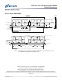
1
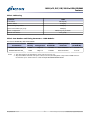
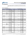
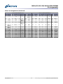
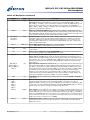
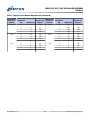
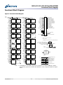
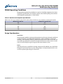
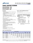
16GB (x72, ECC, DR) 288-Pin DDR4 RDIMM
Features
DDR4 SDRAM RDIMM
MTA36ASF2G72PZ – 16GB
Features
Figure 1: 288-Pin RDIMM (MO-309, R/C-B)
• DDR4 functionality and operations supported as
defined in the component data sheet
• 288-pin, registered dual in-line memory module
(RDIMM)
• Fast data transfer rates: PC4-2400 or PC4-2133
• 16GB (2 Gig x 72)
• VDD = 1.20V (NOM)
• VPP = 2.5V (NOM)
• VDDSPD = 2.5V (NOM)
• Supports ECC error detection and correction
• Nominal and dynamic on-die termination (ODT) for
data, strobe, and mask signals
• Low-power auto self refresh (LPASR)
• On-die V REFDQ generation and calibration
• Dual-rank
• On-board I2C temperature sensor with integrated
serial presence-detect (SPD) EEPROM
• 16 internal banks; 4 groups of 4 banks each
• Fixed burst chop (BC) of 4 and burst length (BL) of 8
via the mode register set (MRS)
• Selectable BC4 or BL8 on-the-fly (OTF)
• Gold edge contacts
• Halogen-free
• Fly-by topology
• Terminated control, command, and address bus
Module height: 31.25mm (1.23in)
Options
Marking
• Operating temperature
– Commercial (0°C ≤ T OPER ≤ 95°C)
• Package
– 288-pin DIMM (halogen-free)
• Frequency/CAS latency
– 0.83ns @ CL = 17(DDR4-2400)
– 0.93ns @ CL = 15 (DDR4-2133)
None
Z
-2G3
-2G1
Table 1: Key Timing Parameters
Data Rate (MT/s)
Industry
Speed NomenGrade clature
CL =
20,
CL =
19
CL =
18
CL =
17
CL =
16
CL =
15
CL =
14
CL = CL =
13
12
CL =
11
CL =
10
tRCD
tRC
(ns)
(ns)
-2G6
PC4-2666
2666
2666
2400
2133
2133
1866
1866 1600
–
1333
–
14.16 14.16
46.16
-2G4
PC4-2400
–
2400
2400
2400
2133
1866
1866 1600
1600
–
1333
13.32 13.32
45.32
-2G3
PC4-2400
–
2400
2400
2133
2133
1866
1866 1600
1600
1333
–
14.16 14.16
46.16
-2G1
PC4-2133
–
–
–
2133
2133
1866
1866 1600
1600
–
1333
13.5
46.5
PDF: 09005aef84f8c349
asf36c2gx72pz.pdf - Rev. F 2/15 EN
1
CL = 9 (ns)
tRP
13.5
Micron Technology, Inc. reserves the right to change products or specifications without notice.
© 2012 Micron Technology, Inc. All rights reserved.
Products and specifications discussed herein are subject to change by Micron without notice.
16GB (x72, ECC, DR) 288-Pin DDR4 RDIMM
Features
Table 2: Addressing
Parameter
16GB
Row address
64K A[15:0]
Column address
1K A[9:0]
Device bank group address
4 BG[1:0]
Device bank address per group
4 BA[1:0]
Device configuration
4Gb (1 Gig x 4), 16 banks
Module rank address
2 CS_n[1:0]
Table 3: Part Numbers and Timing Parameters – 16GB Modules
Base device: MT40A1G4,1 4Gb DDR4 SDRAM
Module
Part Number2
Density
Configuration
Module
Bandwidth
Memory Clock/
Data Rate
Clock Cycles
(CL-tRCD-tRP)
MTA36ASF2G72PZ-2G3__
16GB
2 Gig x 72
19.2 GB/s
0.83ns/2400 MT/s
17-17-17
MTA36ASF2G72PZ-2G1__
16GB
2 Gig x 72
17.0 GB/s
0.93ns/2133 MT/s
15-15-15
Notes:
1. The data sheet for the base device can be found on micron.com.
2. All part numbers end with a two-place code (not shown) that designates component and PCB revisions.
Consult factory for current revision codes. Example: MTA36ASF2G72PZ-2G3A1.
PDF: 09005aef84f8c349
asf36c2gx72pz.pdf - Rev. F 2/15 EN
2
Micron Technology, Inc. reserves the right to change products or specifications without notice.
© 2012 Micron Technology, Inc. All rights reserved.
16GB (x72, ECC, DR) 288-Pin DDR4 RDIMM
Pin Assignments
Pin Assignments
The pin assignment table below is a comprehensive list of all possible pin assignments
for DDR4 RDIMM modules. See Functional Block Diagram for pins specific to this module.
Table 4: Pin Assignments
288-Pin DDR4 RDIMM Front
288-Pin DDR4 RDIMM Back
Pin
Symbol
Pin
Symbol
Pin
Symbol
Pin
Symbol
Pin
Symbol
Pin
Symbol
Pin
Symbol
Pin
Symbol
1
NC
37
VSS
73
VDD
109
Vss
145
NC
181
DQ29
217
VDD
253
DQ41
2
VSS
38
DQ24
74
CK0_t
110 DQS14_t/
TDQS14_t
146
VREFCA
182
VSS
218
CK1_t
254
VSS
3
DQ4
39
VSS
75
CK0_c
111 DQS14_c/
TDQS14_c
147
VSS
183
DQ25
219
CK1_c
255
DQS5_c
4
VSS
40
DQS12_t/
TDQS12_t
76
VDD
112
VSS
148
DQ5
184
VSS
220
VDD
256
DQS5_t
5
DQ0
41
DQS12_c/
TDQS12_c
77
VTT
113
DQ46
149
VSS
185
DQS3_c
221
VTT
257
VSS
6
VSS
42
VSS
78
EVENT_n
114
VSS
150
DQ1
186
DQS3_t
222
PARITY
258
DQ47
7
DQS9_t/
TDQS9_t
43
DQ30
79
A0
115
DQ42
151
VSS
187
VSS
223
VDD
259
VSS
8
DQS09_c/
TDQS9_c
44
VSS
80
VDD
116
VSS
152
DQS0_c
188
DQ31
224
BA1
260
DQ43
9
VSS
45
DQ26
81
BA0
117
DQ52
153
DQS0_t
189
VSS
225
A10/
AP
261
VSS
10
DQ6
46
VSS
82
RAS_n/
A16
118
VSS
154
VSS
190
DQ27
226
VDD
262
DQ53
11
VSS
47
CB4
83
VDD
119
DQ48
155
DQ7
191
VSS
227
NC
263
VSS
12
DQ2
48
VSS
84
CS0_n
120
VSS
156
VSS
192
CB5
228
WE_n/
A14
264
DQ49
13
VSS
49
CB0
85
VDD
121 DQS15_t/
TDQS15_t
157
DQ3
193
VSS
229
VDD
265
VSS
14
DQ12
50
VSS
86
CAS_n/
A15
122 DQS15_c/
TDQS15_c
158
VSS
194
CB1
230
NC
266
DQS6_c
15
VSS
51
DQS17_t/
TDQS17_t
87
ODT0
123
VSS
159
DQ13
195
VSS
231
VDD
267
DQS6_t
16
DQ8
52
DQS17_c/
TDQS17_c
88
VDD
124
DQ54
160
VSS
196
DQS8_c
232
A13
268
VSS
17
VSS
53
VSS
89
CS1_n/
NC
125
VSS
161
DQ9
197
DQS8_t
233
VDD
269
DQ55
18
DQS10_t/
TDQS10_t
54
CB6
90
VDD
126
DQ50
162
VSS
198
VSS
234
A17
270
VSS
19
DQS10_c/
TDQS10_c
55
VSS
91
ODT1/
NC
127
VSS
163
DQS1_c
199
CB7
235
NC/
C2
271
DQ51
20
VSS
56
CB2
92
VDD
128
DQ60
164
DQS1_t
200
VSS
236
VDD
272
VSS
21
DQ14
57
VSS
93
CS2_n/
C0
129
VSS
165
VSS
201
CB3
237
CS3_n/
C1, NC
273
DQ61
22
VSS
58
RESET_n
94
VSS
130
DQ56
166
DQ15
202
VSS
238
SA2
274
VSS
23
DQ10
59
VDD
95
DQ36
131
VSS
167
VSS
203
CKE1/
NC
239
VSS
275
DQ57
24
VSS
60
CKE0
96
VSS
168
DQ11
204
VDD
240
DQ37
276
VSS
PDF: 09005aef84f8c349
asf36c2gx72pz.pdf - Rev. F 2/15 EN
132 DQS16_t/
TDQS16_t
3
Micron Technology, Inc. reserves the right to change products or specifications without notice.
© 2012 Micron Technology, Inc. All rights reserved.
16GB (x72, ECC, DR) 288-Pin DDR4 RDIMM
Pin Assignments
Table 4: Pin Assignments (Continued)
288-Pin DDR4 RDIMM Front
288-Pin DDR4 RDIMM Back
Pin
Symbol
Pin
Symbol
Pin
Symbol
25
DQ20
61
VDD
97
DQ32
26
VSS
62
ACT_n
98
VSS
27
DQ16
63
BG0
99
28
VSS
64
VDD
100 DQS13_c/ 136
TDQS13_c
29
DQS11_t/
TDQS11_t
65
30
DQS11_c/
TDQS11_c
66
A9
31
VSS
67
VDD
A12/BC_n 101
Pin
Symbol
Pin
Symbol
Pin
Symbol
Pin
Symbol
133 DQS16_c/
TDQS16_c
Pin
169
VSS
205
NC
241
VSS
277
DQS7_c
134
VSS
170
DQ21
206
VDD
242
DQ33
278
DQS7_t
DQ62
171
VSS
207
BG1
243
VSS
279
VSS
VSS
172
DQ17
208
ALERT_n
244
DQS4_c
280
DQ63
DQS13_t/ 135
TDQ13_t
Symbol
VSS
137
DQ58
173
VSS
209
VDD
245
DQS4_t
281
VSS
102
DQ38
138
VSS
174
DQS2_c
210
A11
246
VSS
282
DQ59
103
Vss
139
SA0
175
DQS2_t
211
A7
247
DQ39
283
VSS
32
DQ22
68
A8
104
DQ34
140
SA1
176
VSS
212
VDD
248
VSS
284
VDDSPD
33
VSS
69
A6
105
VSS
141
SCL
177
DQ23
213
A5
249
DQ35
285
SDA
34
DQ18
70
VDD
106
DQ44
142
VPP
178
VSS
214
A4
250
VSS
286
VPP
35
VSS
71
A3
107
VSS
143
VPP
179
DQ19
215
VDD
251
DQ45
287
VPP
36
DQ28
72
A1
108
DQ40
144
NC
180
VSS
216
A2
252
VSS
288
VPP
PDF: 09005aef84f8c349
asf36c2gx72pz.pdf - Rev. F 2/15 EN
4
Micron Technology, Inc. reserves the right to change products or specifications without notice.
© 2012 Micron Technology, Inc. All rights reserved.
16GB (x72, ECC, DR) 288-Pin DDR4 RDIMM
Pin Descriptions
Pin Descriptions
The pin description table below is a comprehensive list of all possible pins for DDR4
modules. All pins listed may not be supported on this module. See Functional Block Diagram for pins specific to this module.
Table 5: Pin Descriptions
Symbol
Type
Description
Ax
Input
Address inputs: Provide the row address for ACTIVATE commands and the column address for
READ/WRITE commands in order to select one location out of the memory array in the respective bank (A10/AP, A12/BC_n, WE_n/A14, CAS_n/A15, and RAS_n/A16 have additional functions;
see individual entries in this table). The address inputs also provide the op-code during the
MODE REGISTER SET command. A17 is only defined for x4 SDRAM.
A10/AP
Input
Auto precharge: A10 is sampled during READ and WRITE commands to determine whether an
auto precharge should be performed on the accessed bank after a READ or WRITE operation
(HIGH = auto precharge; LOW = no auto precharge). A10 is sampled during a PRECHARGE command to determine whether the precharge applies to one bank (A10 LOW) or all banks (A10
HIGH). If only one bank is to be precharged, the bank is selected by the bank group and bank
addresses.
A12/BC_n
Input
Burst chop: A12/BC_n is sampled during READ and WRITE commands to determine if burst
chop (on-the-fly) will be performed (HIGH = no burst chop; LOW = burst- chopped). See Command Truth Table in the DDR4 component data sheet.
ACT_n
Input
Command input: ACT_n defines the ACTIVATE command being entered along with CS_n. The
input into RAS_n/A16, CAS_n/A15, and WE_n/A14 are considered as row address A16, A15, and
A14. See Command Truth Table.
BAx
Input
Bank address inputs: Define the bank (with a bank group) to which an ACTIVATE, READ,
WRITE, or PRECHARGE command is being applied. Also determine which mode register is to be
accessed during a MODE REGISTER SET command.
BGx
Input
Bank group address inputs: Define the bank group to which a REFRESH, ACTIVATE, READ,
WRITE, or PRECHARGE command is being applied. Also determine which mode register is to be
accessed during a MODE REGISTER SET command. BG[1:0] are used in the x4 and x8 configurations. x16-based SDRAM only has BG0.
C0, C1, C2
Input
Chip ID: These inputs are used only when devices are stacked; that is, 2H, 4H, and 8H stacks for
x4 and x8 configurations using through-silicon vias (TSVs). These pins are not used in the x16
configuration. Some DDR4 modules support a traditional DDP package, which uses CS1_n,
CKE1, and ODT1 to control the second die. All other stack configurations, such as a 4H or 8H,
are assumed to be single-load (master/slave) type configurations where C0, C1, and C2 are used
as chip ID selects in conjunction with a single CS_n, CKE, and ODT. Chip ID is considered part of
the command code.
CKx_t
CKx_c
Input
Clock: Differential clock inputs. All address, command, and control input signals are sampled
on the crossing of the positive edge of CK_t and the negative edge of CK_c.
CKEx
Input
Clock enable: CKE HIGH activates and CKE LOW deactivates the internal clock signals, device
input buffers, and output drivers. Taking CKE LOW provides PRECHARGE POWER-DOWN and
SELF REFRESH operations (all banks idle), or active power-down (row active in any bank). CKE is
asynchronous for self refresh exit. After VREFCA has become stable during the power-on and initialization sequence, it must be maintained during all operations (including SELF REFRESH). CKE
must be maintained HIGH throughout read and write accesses. Input buffers (excluding CK_t,
CK_c, ODT, RESET_n, and CKE) are disabled during power-down. Input buffers (excluding CKE
and RESET#) are disabled during self refresh.
CSx_n
Input
Chip select: All commands are masked when CS_n is registered HIGH. CS_n provides external
rank selection on systems with multiple ranks. CS_n is considered part of the command code
(CS2_n and CS3_n are not used on UDIMMs).
(RDIMM/LRDIMM only)
PDF: 09005aef84f8c349
asf36c2gx72pz.pdf - Rev. F 2/15 EN
5
Micron Technology, Inc. reserves the right to change products or specifications without notice.
© 2012 Micron Technology, Inc. All rights reserved.
16GB (x72, ECC, DR) 288-Pin DDR4 RDIMM
Pin Descriptions
Table 5: Pin Descriptions (Continued)
Symbol
Type
Description
ODTx
Input
On-die termination: ODT (registered HIGH) enables termination resistance internal to the
DDR4 SDRAM. When enabled, ODT (RTT) is applied only to each DQ, DQS_t, DQS_c, DM_n/
DBI_n/TDQS_t, and TDQS_c signal for x4 and x8 configurations (when the TDQS function is enabled via the mode register). For the x16 configuration, RTT is applied to each DQ, DQSU_t,
DQSU_c, DQSL_t, DQSL_c, UDM_n, and LDM_n signal. The ODT pin will be ignored if the mode
registers are programmed to disable RTT.
PARITY
Input
Parity for command and address: This function can be enabled or disabled via the mode
register. When enabled in MR5, the DRAM calculates parity with ACT_n, RAS_n/A16, CAS_n/A15,
WE_n/A14, BG[1:0], BA[1:0], A[16:0]. Input parity should be maintained at the rising edge of the
clock and at the same time as command and address with CS_n LOW.
RAS_n/A16
CAS_n/A15
WE_n/A14
Input
Command inputs: RAS_n/A16, CAS_n/A15, and WE_n/A14 (along with CS_n) define the command and/or address being entered and have multiple functions. For example, for activation
with ACT_n LOW, these are addresses like A16, A15, and A14, but for a non-activation command with ACT_n HIGH, these are command pins for READ, WRITE, and other commands defined in Command Truth Table.
RESET_n
CMOS Input
SAx
Input
Serial address inputs: Used to configure the temperature sensor/SPD EEPROM address range
on the I2C bus.
SCL
Input
Serial clock for temperature sensor/SPD EEPROM: Used to synchronize communication to
and from the temperature sensor/SPD EEPROM on the I2C bus.
DQx, CBx
I/O
Data input/output and check bit input/output: Bidirectional data bus. DQ represents
DQ[3:0], DQ[7:0], and DQ[15:0] for the x4, x8, and x16 configurations, respectively. If cyclic redundancy checksum (CRC) is enabled via the mode register, the CRC code is added at the end of
the data burst. Any one or all of DQ0, DQ1, DQ2, or DQ3 may be used for monitoring of internal VREF level during test via mode register setting MR[4] A[4] = HIGH; training times change
when enabled.
DM_n/DBI_n/
TDQS_t (DMU_n,
DBIU_n), (DML_n/
DBIl_n)
I/O
Input data mask and data bus inversion: DM_n is an input mask signal for write data. Input
data is masked when DM_n is sampled LOW coincident with that input data during a write access. DM_n is sampled on both edges of DQS. DM is multiplexed with the DBI function by the
mode register A10, A11, and A12 settings in MR5. For a x8 device, the function of DM or TDQS
is enabled by the mode register A11 setting in MR1. DBI_n is an input/output identifying
whether to store/output the true or inverted data. If DBI_n is LOW, the data will be stored/
output after inversion inside the DDR4 device and not inverted if DBI_n is HIGH. TDQS is only
supported in x8 SDRAM configurations (TDQS is not valid for UDIMMs).
SDA
I/O
Serial Data: Bidirectional signal used to transfer data in or out of the EEPROM or EEPROM/TS
combo device.
DQS_t
DQS_c
DQSU_t
DQSU_c
DQSL_t
DQSL_c
I/O
Data strobe: Output with read data, input with write data. Edge-aligned with read data, centered-aligned with write data. For x16 configurations, DQSL corresponds to the data on
DQ[7:0], and DQSU corresponds to the data on DQ[15:8]. For the x4 and x8 configurations, DQS
corresponds to the data on DQ[3:0] and DQ[7:0], respectively. DDR4 SDRAM supports a differential data strobe only and does not support a single-ended data strobe.
ALERT_n
Output
Alert output: Possesses functions such as CRC error flag and command and address parity error
flag as output signal. If a CRC error occurs, ALERT_n goes LOW for the period time interval and
returns HIGH. If an error occurs during a command address parity check, ALERT_n goes LOW until the on-going DRAM internal recovery transaction is complete. During connectivity test mode,
this pin functions as an input. Use of this signal is system-dependent. If not connected as signal,
ALERT_n pin must be connected to VDD on DIMMs.
EVENT_n
Output
Temperature event: The EVENT_n pin is asserted by the temperature sensor when critical temperature thresholds have been exceeded. This pin has no function (NF) on modules without
temperature sensors.
PDF: 09005aef84f8c349
asf36c2gx72pz.pdf - Rev. F 2/15 EN
Active LOW asynchronous reset: Reset is active when RESET_n is LOW and inactive when RESET_n is HIGH. RESET_n must be HIGH during normal operation.
6
Micron Technology, Inc. reserves the right to change products or specifications without notice.
© 2012 Micron Technology, Inc. All rights reserved.
16GB (x72, ECC, DR) 288-Pin DDR4 RDIMM
Pin Descriptions
Table 5: Pin Descriptions (Continued)
Symbol
Type
Description
TDQS_t
TDQS_c
Output
Termination data strobe: When enabled via the mode register, the DRAM device enables the
same RTT termination resistance on TDQS_t and TDQS_c that is applied to DQS_t and DQS_c.
When the TDQS function is disabled via the mode register, the DM/TDQS_t pin provides the data mask (DM) function, and the TDQS_c pin is not used. The TDQS function must be disabled in
the mode register for both the x4 and x16 configurations. The DM function is supported only in
x8 and x16 configurations. DM, DBI, and TDQS are a shared pin and are enabled/disabled by
mode register settings. For more information about TDQS, see the DDR4 DRAM component data sheet (TDQS_t and TDQS_c are not valid for UDIMMs).
VDD
Supply
Module power supply: 1.2V (TYP).
VPP
Supply
DRAM activating power supply: 2.5V –0.125V / +0.250V.
VREFCA
Supply
Reference voltage for control, command, and address pins.
VSS
Supply
Ground.
(x8 DRAM-based
RDIMM only)
VTT
Supply
Power supply for termination of address, command, and control VDD/2.
VDDSPD
Supply
Power supply used to power the I2C bus for SPD.
RFU
–
Reserved for future use.
NC
–
No connect: No internal electrical connection is present.
NF
–
No function: May have internal connection present, but has no function.
PDF: 09005aef84f8c349
asf36c2gx72pz.pdf - Rev. F 2/15 EN
7
Micron Technology, Inc. reserves the right to change products or specifications without notice.
© 2012 Micron Technology, Inc. All rights reserved.
16GB (x72, ECC, DR) 288-Pin DDR4 RDIMM
DQ Map
DQ Map
Table 6: Component-to-Module DQ Map Front
Component
Reference
Number
Component
DQ
U1
U3
U5
U8
U10
U12
U14
U17
PDF: 09005aef84f8c349
asf36c2gx72pz.pdf - Rev. F 2/15 EN
Module DQ
Module Pin
Number
Component
Reference
Number
Component
DQ
Module DQ
Module Pin
Number
0
3
157
U2
0
14
21
1
0
5
1
13
159
2
2
12
2
15
166
3
1
150
3
12
14
0
22
32
0
30
43
1
21
170
1
28
36
2
23
177
2
31
188
3
20
25
3
29
181
0
CB3
201
0
38
102
1
CB0
49
1
37
240
2
CB2
56
2
39
247
3
CB1
194
3
36
95
0
43
260
0
55
269
1
41
253
1
52
117
2
42
115
2
54
124
3
40
108
3
53
262
0
62
135
0
6
10
1
60
128
1
5
148
2
63
280
2
7
155
3
61
273
3
4
3
0
11
168
0
17
172
1
9
161
1
18
34
2
10
23
2
16
27
3
8
16
3
19
179
0
27
190
0
CB5
192
1
25
183
1
CB6
54
2
26
45
2
CB4
47
3
24
38
3
CB7
199
0
32
97
0
46
113
1
34
104
1
45
251
2
33
242
2
47
258
3
35
249
3
44
106
U4
U7
U9
U11
U13
U15
U18
8
Micron Technology, Inc. reserves the right to change products or specifications without notice.
© 2012 Micron Technology, Inc. All rights reserved.
16GB (x72, ECC, DR) 288-Pin DDR4 RDIMM
DQ Map
Table 6: Component-to-Module DQ Map Front (Continued)
Component
Reference
Number
Component
DQ
Module DQ
Module Pin
Number
Component
Reference
Number
Component
DQ
Module DQ
Module Pin
Number
U19
0
51
271
U20
0
58
137
1
48
119
1
56
130
2
50
126
2
59
282
3
49
264
3
57
275
Table 7: Component-to-Module DQ Map Back
Component
Reference
Number
Component
DQ
U21
U23
U25
U27
U29
U31
PDF: 09005aef84f8c349
asf36c2gx72pz.pdf - Rev. F 2/15 EN
Module DQ
Module Pin
Number
Component
Reference
Number
Component
DQ
Module DQ
Module Pin
Number
0
60
128
U22
0
52
117
1
62
135
1
55
269
2
61
273
2
53
262
3
63
280
3
54
124
0
41
253
0
37
240
1
43
260
1
38
102
2
40
108
2
36
95
3
42
115
3
39
247
0
CB0
49
0
28
36
1
CB3
201
1
30
43
2
CB1
194
2
29
181
3
CB2
56
3
31
188
0
21
170
0
13
159
1
22
32
1
14
21
2
20
25
2
12
14
3
23
177
3
15
166
0
0
5
0
56
130
1
3
157
1
58
137
2
1
150
2
57
275
3
2
12
3
59
282
0
48
119
0
45
251
1
51
271
1
46
113
2
49
264
2
44
106
3
50
126
3
47
258
U24
U26
U28
U30
U32
9
Micron Technology, Inc. reserves the right to change products or specifications without notice.
© 2012 Micron Technology, Inc. All rights reserved.
16GB (x72, ECC, DR) 288-Pin DDR4 RDIMM
DQ Map
Table 7: Component-to-Module DQ Map Back (Continued)
Component
Reference
Number
Component
DQ
U33
U35
U37
PDF: 09005aef84f8c349
asf36c2gx72pz.pdf - Rev. F 2/15 EN
Module DQ
Module Pin
Number
Component
Reference
Number
Component
DQ
Module DQ
Module Pin
Number
0
34
104
U34
0
CB6
54
1
32
97
1
CB5
192
2
35
249
2
CB7
199
3
33
242
3
CB4
47
0
25
183
0
18
34
1
27
190
1
17
172
2
24
38
2
19
179
3
26
45
3
16
27
0
9
161
0
5
148
1
11
168
1
6
10
2
8
16
2
4
3
3
10
23
3
7
155
U36
U38
10
Micron Technology, Inc. reserves the right to change products or specifications without notice.
© 2012 Micron Technology, Inc. All rights reserved.
16GB (x72, ECC, DR) 288-Pin DDR4 RDIMM
Functional Block Diagram
Functional Block Diagram
Figure 2: Functional Block Diagram
U16
A/BCS0_n
A/BCS1_n
DQS9_t
DQS9_c
DQS0_t
DQS0_c
CS_n DQS_t DQS_c
DQ0
DQ1
DQ2
DQ3
Vss
DQS1_t
DQS1_c
DQ
DQ
DQ
DQ
ZQ
DQ8
DQ9
DQ10
DQ11
Vss
DQ
DQ
DQ
DQ
ZQ
U1
CS_n DQS_t DQS_c
DQ
DQ
DQ
DQ
U29
ZQ
VSS
CS_n DQS_t DQS_c
U12
CS_n DQS_t DQS_c
DQ
DQ
DQ
DQ
DQ16
DQ17
DQ18
DQ19
Vss
DQS3_t
DQS3_c
DQ24
DQ25
DQ26
DQ27
Vss
DQS8_t
DQS8_c
CB0
CB1
CB2
CB3
Vss
ZQ
VSS
CS_n DQS_t DQS_c
DQ
DQ
DQ
DQ
ZQ
U13
CS_n DQS_t DQS_c
DQ
DQ
DQ
DQ
U36
ZQ
VSS
CS_n DQS_t DQS_c
DQ
DQ
DQ
DQ
ZQ
U14
CS_n DQS_t DQS_c
DQ
DQ
DQ
DQ
ZQ
VSS
CS_n DQS_t DQS_c
DQ
DQ
DQ
DQ
ZQ
U5
DQS5_t
DQS5_c
DQ40
DQ41
DQ42
DQ43
Vss
U17
CS_n DQS_t DQS_c
DQ
DQ
DQ
DQ
U33
ZQ
CS_n DQS_t DQS_c
U8
DQ48
DQ49
DQ50
DQ51
Vss
ZQ
VSS
DQS7_t
DQS7_c
DQ56
DQ57
DQ58
DQ59
Vss
CS_n DQS_t DQS_c
DQ
DQ
DQ
DQ
ZQ
U19
CS_n DQS_t DQS_c
DQ
DQ
DQ
DQ
U31
VSS
DQ
DQ
DQ
DQ
ZQ
U20
DQ
DQ
DQ
DQ
ZQ
U2
DQ60
DQ61
DQ62
DQ63
Vss
U30
ZQ
CS_n DQS_t DQS_c
DQ
DQ
DQ
DQ
PDF: 09005aef84f8c349
asf36c2gx72pz.pdf - Rev. F 2/15 EN
ZQ
VSS
CS_n DQS_t DQS_c
DQ
DQ
DQ
DQ
ZQ
U3
CS_n DQS_t DQS_c
DQ
DQ
DQ
DQ
U27
ZQ
CS_n DQS_t DQS_c
DQ
DQ
DQ
DQ
ZQ
U4
CS_n DQS_t DQS_c
DQ
DQ
DQ
DQ
E
G
I
S
T
E
R
&
P
L
L
RESET_CONN
DDR4 SDRAM
CK[1:0]_c
RESET_DRAM: DDR4 SDRAM
ZQ
U26
VSS
ZQ
Rank 0: U1–U5, U7–U15, U17–U20
Rank 1: U21–38
U15
CS_n DQS_t DQS_c
DQ
DQ
DQ
DQ
U34
Command, control, address, and clock line terminations:
ZQ
VSS
CS_n DQS_t DQS_c
DQ
DQ
DQ
DQ
ZQ
CK[1:0]_t
CK_t
CK_c
VSS
DQ
DQ
DQ
DQ
ZQ
A/BCS0_n: Rank 0
A/BCS1_n: Rank 1
A/BBA[1:0]: DDR4 SDRAM
A/BBG[1:0]: DDR4 SDRAM
A/BACT_n: DDR4 SDRAM
A/BA[17,13:0]: DDR4 SDRAM
A/B-RAS_n/A16: DDR4 SDRAM
A/B-CAS_n/A15: DDR4 SDRAM
A/B-WE_n/A14: DDR4 SDRAM
A/BCKE0: Rank 0
A/BCKE1: Rank 1
A/BODT0: Rank 0
A/BODT1: Rank 1
A/BPAR: DDR4 SDRAM
C[2:0]: DDR4 SDRAM
ALERT_DRAM: DDR4 SDRAM
R
SA0
SA1
SA2
SCL
SDA
VSS
U7
CS_n DQS_t DQS_c
DQ
DQ
DQ
DQ
A/BCS_n[1:0], A/BBA[1:0]A/BBG[1:0],
A/BACT_n, A/BA[17, 13:0], A/B-RAS_n/A16,
A/B-CAS_n/A15, A/B-WE_n/A14,
A/BCKE[1:0], A/BODT[1:0]
U24
DDR4
SDRAM
VTT
DDR4
SDRAM
CK[3:0]_t
CK[3:0]_c
ZQ
VDD
VSS
DQ
DQ
DQ
DQ
ZQ
U18
CS_n DQS_t DQS_c
DQ
DQ
DQ
DQ
U6
U32
SCL
ZQ
CS_n DQS_t DQS_c
DQ
DQ
DQ
DQ
ZQ
U9
EVENT#
U22
VDDSPD
ZQ
VSS
CS_n DQS_t DQS_c
CS_n DQS_t DQS_c
DQ
DQ
DQ
DQ
ZQ
DQ
DQ
DQ
DQ
U10
SDA
A1 A2
SA0 SA1 SA2
CS_n DQS_t DQS_c
DQ
DQ
DQ
DQ
SPD EEPROM/
Temperature
sensor
EVT A0
VSS
VDD
VTT
U21
VREFCA
ZQ
VSS
VSS
Note:
U28
DQS16_t
DQS16_c
CS_n DQS_t DQS_c
DQ
DQ
DQ
DQ
CS_n DQS_t DQS_c
DQS15_t
DQS15_c
DQ52
DQ53
DQ54
DQ55
Vss
ZQ
CS_n DQS_t DQS_c
VSS
DQS14_t
DQS14_c
DQ44
DQ45
DQ46
DQ47
Vss
U23
DQS6_t
DQS6_c
ZQ
CS_n DQS_t DQS_c
CS_n DQS_t DQS_c
DQ
DQ
DQ
DQ
U38
DQS13_t
DQS13_c
DQ36
DQ37
DQ38
DQ39
Vss
VSS
DQ
DQ
DQ
DQ
ZQ
DQ
DQ
DQ
DQ
U11
DQS17_t
DQS17_c
CB4
CB5
CB6
CB7
Vss
U25
ZQ
CS_n DQS_t DQS_c
CS_n DQS_t DQS_c
DQ
DQ
DQ
DQ
ZQ
CS_n DQS_t DQS_c
VSS
DQ
DQ
DQ
DQ
ZQ
DQ20
DQ21
DQ22
DQ23
Vss
DQS12_t
DQS12_c
CS_n DQS_t DQS_c
DQ
DQ
DQ
DQ
CS_n DQS_t DQS_c
DQS11_t
DQS11_c
DQ28
DQ29
DQ30
DQ31
Vss
U35
DQS4_t
DQS4_c
DQ32
DQ33
DQ34
DQ35
Vss
DQ12
DQ13
DQ14
DQ15
Vss
U37
DQS2_t
DQS2_c
DQ4
DQ5
DQ6
DQ7
Vss
DQS10_t
DQS10_c
CS0_n
CS1_n
BA[1:0]
BG[1:0]
ACT_n
A[17, 13:0]
RAS_n/A16
CAS_n/A15
WE_n/A14
CKE0
CKE1
ODT0
ODT1
PAR_IN
C[2:0]
ALERT_CONN
SPD EEPROM/Temp Sensor,
Register
DDR4 SDRAM, Register
Control, command and
address termination
DDR4 SDRAM, Register
VPP
DDR4 SDRAM
VSS
DDR4 SDRAM, Register
1. The ZQ ball on each DDR4 component is connected to an external 240Ω ±1% resistor
that is tied to ground. It is used for the calibration of the component’s ODT and output
driver.
11
Micron Technology, Inc. reserves the right to change products or specifications without notice.
© 2012 Micron Technology, Inc. All rights reserved.
16GB (x72, ECC, DR) 288-Pin DDR4 RDIMM
General Description
General Description
High-speed DDR4 SDRAM modules use DDR4 SDRAM devices with two or four internal
memory bank groups. DDR4 SDRAM modules utilizing 4- and 8-bit-wide DDR4 SDRAM
devices have four internal bank groups consisting of four memory banks each, providing a total of 16 banks. 16-bit-wide DDR4 SDRAM devices have two internal bank
groups consisting of four memory banks each, providing a total of eight banks. DDR4
SDRAM modules benefit from DDR4 SDRAM's use of an 8n-prefetch architecture with
an interface designed to transfer two data words per clock cycle at the I/O pins. A single
READ or WRITE operation for the DDR4 SDRAM effectively consists of a single 8n-bitwide, four-clock data transfer at the internal DRAM core and eight corresponding n-bitwide, one-half-clock-cycle data transfers at the I/O pins.
DDR4 modules use two sets of differential signals: DQS_t and DQS_c to capture data
and CK_t and CK_c to capture commands, addresses, and control signals. Differential
clocks and data strobes ensure exceptional noise immunity for these signals and provide precise crossing points to capture input signals.
Fly-By Topology
DDR4 modules use faster clock speeds than earlier DDR technologies, making signal
quality more important than ever. For improved signal quality, the clock, control, command, and address buses have been routed in a fly-by topology, where each clock, control, command, and address pin on each DRAM is connected to a single trace and terminated (rather than a tree structure, where the termination is off the module near the
connector). Inherent to fly-by topology, the timing skew between the clock and DQS signals can be easily accounted for by using the write-leveling feature of DDR4.
PDF: 09005aef84f8c349
asf36c2gx72pz.pdf - Rev. F 2/15 EN
12
Micron Technology, Inc. reserves the right to change products or specifications without notice.
© 2012 Micron Technology, Inc. All rights reserved.
16GB (x72, ECC, DR) 288-Pin DDR4 RDIMM
Address Mapping to DRAM
Address Mapping to DRAM
Address Mirroring
To achieve optimum routing of the address bus on DDR4 multi rank modules, the address bus will be wired as shown in the table below, or mirrored. For quad rank modules, ranks 1 and 3 are mirrored and ranks 0 and 2 are non-mirrored. Highlighted address pins have no secondary functions allowing for normal operation when crosswired. Data is still read from the same address it was written. However, Load Mode operations require a specific address. This requires the controller to accommodate for a
rank that is "mirrored." Systems may reference DDR4 SPD to determine if the module
has mirroring implemented or not. See the JEDEC DDR4 SPD specification for more details.
Table 8: Address Mirroring
Edge Connector Pin
DRAM Pin, Non-mirrored
DRAM Pin, Mirrored
A0
A0
A0
A1
A1
A1
A2
A2
A2
A3
A3
A4
A4
A4
A3
A5
A5
A6
A6
A6
A5
A7
A7
A8
A8
A8
A7
A9
A9
A9
A10
A10
A10
A11
A11
A13
A13
A13
A11
A12
A12
A12
A14
A14
A14
A15
A15
A15
A16
A16
A16
A17
A17
A17
BA0
BA0
BA1
BA1
BA1
BA0
BG0
BG0
BG1
BG1
BG1
BG0
Registering Clock Driver Operation
Registered DDR4 SDRAM modules use a registering clock driver device consisting of a
register and a phase-lock loop (PLL). The device complies with the JEDEC DDR4 RCD01
Specification.
PDF: 09005aef84f8c349
asf36c2gx72pz.pdf - Rev. F 2/15 EN
13
Micron Technology, Inc. reserves the right to change products or specifications without notice.
© 2012 Micron Technology, Inc. All rights reserved.
16GB (x72, ECC, DR) 288-Pin DDR4 RDIMM
Registering Clock Driver Operation
To reduce the electrical load on the host memory controller's command, address, and
control bus, Micron's RDIMMs utilize a DDR4 registering clock driver (RCD). The RCD
presents a single load to the controller while redriving signals to the DDR4 SDRAM devices, which helps enable higher densities and increase signal integrity. The RCD also
provides a low-jitter, low-skew PLL that redistributes a differential clock pair to multiple
differential pairs of clock outputs.
Control Words
The RCD device(s) used on DDR4 RDIMMs and LRDIMMs contain configuration registers known as control words, which the host uses to configure the RCD based on criteria
determined by the module design. Control words can be set by the host controller
through either the DRAM address and control bus or the I2C bus interface. The RCD I 2C
bus interface resides on the same I2C bus interface as the module temperature sensor
and EEPROM.
Parity Operations
The RCD includes a parity-checking function that can be enabled or disabled in control
word RC0E. The RCD receives a parity bit at the DPAR input from the memory controller and compares it with the data received on the qualified command and address inputs; it indicates on its open-drain ALERT_n pin whether a parity error has occurred. If
parity checking is enabled, the RCD forwards commands to the SDRAM when no parity
error has occurred. If the parity error function is disabled, the RCD forwards sampled
commands to the SDRAM regardless of whether a parity error has occurred. Parity is also checked during control word WRITE operations unless parity checking is disabled.
Rank Addressing
The chip select pins (CS_n) on Micron's modules are used to select a specific rank of
DRAM. The RDIMM is capable of selecting ranks in one of three different operating
modes, dependant on setting DA[1:0] bits in the DIMM configuration control word located within the RCD. Direct DualCS mode is utilized for single- or dual-rank modules.
For quad-rank modules, either direct or encoded QuadCS mode is used.
PDF: 09005aef84f8c349
asf36c2gx72pz.pdf - Rev. F 2/15 EN
14
Micron Technology, Inc. reserves the right to change products or specifications without notice.
© 2012 Micron Technology, Inc. All rights reserved.
16GB (x72, ECC, DR) 288-Pin DDR4 RDIMM
Temperature Sensor With SPD EEPROM Operation
Temperature Sensor With SPD EEPROM Operation
Thermal Sensor Operations
The integrated thermal sensor continuously monitors the temperature of the module
PCB directly below the device and updates the temperature data register. Temperature
data may be read from the bus host at any time, which provides the host real-time feedback of the module's temperature. Multiple programmable and read-only temperature
registers can be used to create a custom temperature-sensing solution based on system
requirements and JEDEC JC-42.2.
EVENT_n Pin
The temperature sensor also adds the EVENT_n pin (open-drain), which requires a pullup to V DDSPD. EVENT_n is a temperature sensor output used to flag critical events that
can be set up in the sensor’s configuration registers. EVENT_n is not used by the serial
presence-detect (SPD) EEPROM.
EVENT_n has three defined modes of operation: interrupt, comparator, and TCRIT. In
interrupt mode, the EVENT_n pin remains asserted until it is released by writing a 1 to
the clear event bit in the status register. In comparator mode, the EVENT_n pin clears
itself when the error condition is removed. Comparator mode is always used when the
temperature is compared against the TCRIT limit. In TCRIT only mode, the EVENT_n
pin is only asserted if the measured temperature exceeds the TCRIT limit; it then remains asserted until the temperature drops below the TCRIT limit minus the TCRIT
hysteresis.
SPD EEPROM Operation
DDR4 SDRAM modules incorporate SPD. The SPD data is stored in a 512-byte, JEDEC
JC-42.4-compliant EEPROM that is segregated into four 128-byte, write-protectable
blocks. The SPD content is aligned with these blocks as shown in the table below.
Block
Range
Description
0
0–127
1
128–255
080h–0FFh
Module parameters
2
256–319
100h–13Fh
Reserved (all bytes coded as 00h)
320–383
140h–17Fh
Manufacturing information
384–511
180h–1FFh
End-user programmable
3
000h–07Fh
Configuration and DRAM parameters
The first 384 bytes are programmed by Micron to comply with JEDEC standard JC-45,
"Appendix X: Serial Presence Detect (SPD) for DDR4 SDRAM Modules." The remaining
128 bytes of storage are available for use by the customer.
The EEPROM resides on a two-wire I2C serial interface and is not integrated with the
memory bus in any manner. It operates as a slave device in the I2C bus protocol, with all
operations synchronized by the serial clock. Transfer rates of up to 1 MHz are achievable at 2.5V (NOM).
Micron implements reversible software write protection on DDR4 SDRAM-based modules. This prevents the lower 384 bytes (bytes 0 to 383) from being inadvertently programmed or corrupted. The upper 128 bytes remain available for customer use and are
unprotected.
PDF: 09005aef84f8c349
asf36c2gx72pz.pdf - Rev. F 2/15 EN
15
Micron Technology, Inc. reserves the right to change products or specifications without notice.
© 2012 Micron Technology, Inc. All rights reserved.
16GB (x72, ECC, DR) 288-Pin DDR4 RDIMM
Electrical Specifications
Electrical Specifications
Stresses greater than those listed may cause permanent damage to the module. This is a
stress rating only, and functional operation of the module at these or any other conditions outside those indicated in each device's data sheet is not implied. Exposure to absolute maximum rating conditions for extended periods may adversely affect reliability.
Table 9: Absolute Maximum Ratings
Symbol
Parameter
Min
Max
Units
Notes
VDD
VDD supply voltage relative to VSS
–0.4
1.5
V
1
VDDQ
VDDQ supply voltage relative to VSS
–0.4
1.5
V
1
Voltage on VPP pin relative to VSS
–0.4
3.0
V
2
VIN, VOUT Voltage on any pin relative to VSS
–0.4
1.5
V
VPP
Table 10: Operating Conditions
Symbol
Parameter
Min
Nom
Max
Units
Notes
VDD
VDD supply voltage
1.14
1.20
1.26
V
1
VPP
DRAM activating power supply
2.375
2.5
2.75
V
2
0.49 × VDD
0.5 × VDD
0.51 × VDD
V
3
–750
–
750
mA
0.49 × VDD 20mV
0.5 × VDD
0.51 × VDD +
20mV
V
4
–
µA
5
VREFCA(DC) Input reference voltage –
command/address bus
IVTT
Termination reference current from VTT
VTT
Termination reference voltage (DC) –
command/address bus
II
Input leakage current; any input excluding ZQ; 0V <
VIN < 1.1V
–
–
II
Input leakage current; ZQ
–3
–
3
µA
6, 7
DQ leakage; 0V < VIN < VDD
–4
–
4
µA
7
IOZpd
Output leakage current; VOUT = VDD; DQ is disabled
–
–
5
µA
IOZpu
Output leakage current; VOUT = VSS; DQ and ODT
are disabled; ODT is disabled with ODT input HIGH
–
–
50
µA
VREFCA leakage; VREFCA = VDD/2 (after DRAM is initialized)
–2
–
2
µA
II/O
IVREFCA
Notes:
PDF: 09005aef84f8c349
asf36c2gx72pz.pdf - Rev. F 2/15 EN
7
1. VDDQ balls on DRAM are tied to VDD.
2. VPP must be greater than or equal to VDD at all times.
3. VREFCA must not be greater than 0.6 × VDD. When VDD is less than 500mV, VREF may be
less than or equal to 300mV.
4. VTT termination voltages in excess of specification limit adversely affect command and
address signals' voltage margins and reduce timing margins.
5. Command and address inputs are terminated to VDD/2 in the registering clock driver. Input current is dependent on termination resistance set in the registering clock driver.
6. Tied to ground. Not connected to edge connector.
7. Multiply by number of DRAM die on module.
16
Micron Technology, Inc. reserves the right to change products or specifications without notice.
© 2012 Micron Technology, Inc. All rights reserved.
16GB (x72, ECC, DR) 288-Pin DDR4 RDIMM
Electrical Specifications
Table 11: Thermal Characteristics
Symbol
Parameter/Condition
Value
Units
Notes
TC
Commercial operating case temperature
0 to 85
°C
1, 2, 3
>85 to 95
°C
1, 2, 3, 4
0 to 85
°C
5, 6
>85 to 95
°C
5, 6
TOPER
Normal operating temperature range
Extended temperature operating range (optional)
Notes:
PDF: 09005aef84f8c349
asf36c2gx72pz.pdf - Rev. F 2/15 EN
1. Maximum operating case temperature. TC is measured in the center of the package.
2. A thermal solution must be designed to ensure the DRAM device does not exceed the
maximum TC during operation.
3. Device functionality is not guaranteed if the DRAM device exceeds the maximum TC during operation.
4. If TC exceeds 85°C, the DRAM device must be refreshed externally at 2X refresh (a 3.9µs
interval refresh rate).
5. The refresh rate must double when 85°C < TOPER ≤ 95°C.
6. For additional information, refer to technical note TN-00-08: "Thermal Applications,"
available at micron.com.
17
Micron Technology, Inc. reserves the right to change products or specifications without notice.
© 2012 Micron Technology, Inc. All rights reserved.
16GB (x72, ECC, DR) 288-Pin DDR4 RDIMM
DRAM Operating Conditions
DRAM Operating Conditions
Recommended AC operating conditions are given in the DDR4 component data sheets.
Component specifications are available at micron.com. Module speed grades correlate
with component speed grades, as shown below.
Table 12: Module and Component Speed Grades
DDR4 components may exceed the listed module speed grades; module may not be available in all listed speed grades
Module Speed Grade
Component Speed Grade
-2G6
-075
-2G4
-083E
-2G3
-083
-2G1
-093E
-1G9
-107E
Design Considerations
Simulations
Micron memory modules are designed to optimize signal integrity through carefully designed terminations, controlled board impedances, routing topologies, trace length
matching, and decoupling. However, good signal integrity starts at the system level. Micron encourages designers to simulate the signal characteristics of the system's memory bus to ensure adequate signal integrity of the entire memory system.
Power
Operating voltages are specified at the edge connector of the module, not at the DRAM.
Designers must account for any system voltage drops at anticipated power levels to ensure the required supply voltage is maintained.
PDF: 09005aef84f8c349
asf36c2gx72pz.pdf - Rev. F 2/15 EN
18
Micron Technology, Inc. reserves the right to change products or specifications without notice.
© 2012 Micron Technology, Inc. All rights reserved.
16GB (x72, ECC, DR) 288-Pin DDR4 RDIMM
IDD Specifications
IDD Specifications
Table 13: DDR4 IDD Specifications and Conditions – 16GB (Die Revision A)
Values are for the MT40A1G4 DDR4 SDRAM only and are computed from values specified in the 4Gb (1 Gig x 4) component data sheet
Parameter
Symbol
2400
2133
Units
IDD01
One bank ACTIVATE-PRECHARGE current
One bank ACTIVATE-PRECHARGE, word line boost, IPP current
One bank ACTIVATE-READ-PRECHARGE current
IPP0
1728
1620
mA
1
126
126
mA
1
IDD1
1800
1720
mA
Precharge standby current
IDD2N
2
1800
1656
mA
Precharge standby ODT current
IDD2NT1
1620
1512
mA
2
1152
1080
mA
2
1476
1404
mA
2
Precharge power-down current
IDD2P
Precharge quite standby current
IDD2Q
Active standby current
IDD3N
2412
2268
mA
Active standby IPP current
IPP3N2
108
108
mA
2
1586
1584
mA
1
Active power-down current
IDD3P
Burst read current
IDD4R
3456
3240
mA
Burst read IDDQ current
IDDQ4R1
1296
1188
mA
Burst write current
IDD4W1
3816
3420
mA
Burst refresh current (1 x REF)
IDD5B1
4032
3960
mA
1
Burst refresh IPP current (1 x REF)
IPP5B
450
450
mA
Self refresh current: Normal temperature range (0–85°C)
IDD6N
2
720
720
mA
Self refresh current: Extended temperature range (0–95°C)
IDD6E2
972
972
mA
Self refresh current: Reduced temperature range (0–45°C)
IDD6R2
360
360
mA
2
324
324
mA
Auto self refresh current (45°C)
IDD6A
2
360
360
mA
Auto self refresh current (75°C)
IDD6A2
576
576
mA
1
4356
3870
mA
1
306
270
mA
2
648
648
mA
Auto self refresh current (25°C)
IDD6A
Bank interleave read current
IDD7
Bank interleave read IPP current
IPP7
Maximum power-down current
Notes:
PDF: 09005aef84f8c349
asf36c2gx72pz.pdf - Rev. F 2/15 EN
IDD8
1. One module rank in the active IDD/PP, the other rank in IDD2P/PP3N.
2. All ranks in this IDD/PP condition.
19
Micron Technology, Inc. reserves the right to change products or specifications without notice.
© 2012 Micron Technology, Inc. All rights reserved.
16GB (x72, ECC, DR) 288-Pin DDR4 RDIMM
Registering Clock Driver Specifications
Registering Clock Driver Specifications
Table 14: Registering Clock Driver Electrical Characteristics
DDR4 RCD01 devices or equivalent
Parameter
Symbol
Pins
Min
Nom
Max
Units
DC supply voltage
VDD
–
1.14
1.2
1.26
V
DC reference voltage
VREF
VREFCA
0.49 × VDD
0.5 × VDD
0.51 × VDD
V
DC termination
voltage
VTT
–
VREF - 40mV
VREF
VREF + 40mV
V
High-level input
voltage
VIH. CMOS
DRST_n
0.65 × VDD
–
VDD
V
Low-level input
voltage
VIL. CMOS
0
–
0.35 × VDD
V
DRST_n pulse width
tINIT_Power_stable
–
1.0
–
–
µs
AC high-level output
voltage
VOH(AC)
All outputs except
ALERT_n
VTT + (0.15 × VDD)
–
–
V
AC low-level output
voltage
VOL(AC)
–
–
VTT + (0.15 x VDD)
V
AC differential output high measurement level (for output slew rate)
VOHdiff(AC)
–
0.3 × VDD
–
mV
AC differential output low measurement level (for output slew rate)
VOLdiff(AC)
–
–0.3 × VDD
–
mV
Note:
PDF: 09005aef84f8c349
asf36c2gx72pz.pdf - Rev. F 2/15 EN
Yn_t - Yn_c, BCK_t BCK_c
1. Timing and switching specifications for the register listed are critical for proper operation of DDR4 SDRAM RDIMMs. These are meant to be a subset of the parameters for the
specific device used on the module. See the JEDEC RCD01 specification for complete operating electrical characteristics. Registering clock driver parametric values are specified
for device default control word settings, unless otherwise stated. The RC0A control
word setting does not affect parametric values.
20
Micron Technology, Inc. reserves the right to change products or specifications without notice.
© 2012 Micron Technology, Inc. All rights reserved.
16GB (x72, ECC, DR) 288-Pin DDR4 RDIMM
Temperature Sensor With SPD EEPROM
Temperature Sensor With SPD EEPROM
The temperature sensor continuously monitors the module's temperature and can be
read back at any time over the I2C bus shared with the serial presence-detect (SPD) EEPROM. Refer to JEDEC JC-42.4 EE1004 and TSE2004 device specifications for complete
details.
SPD Data
For the latest SPD data, refer to Micron's SPD page: micron.com/SPD.
Table 15: Temperature Sensor With SPD EEPROM Operating Conditions
Parameter/Condition
Symbol
Min
Nom
Max
Units
VDDSPD
–
2.5
–
V
Input low voltage: logic 0; all inputs
VIL
–0.5
–
VDDSPD × 0.3
V
Input high voltage: logic 1; all inputs
VIH
VDDSPD × 0.7
–
VDDSPD + 0.5
V
Output low voltage: 3mA sink current VDDSPD > 2V
Supply voltage
VOL
–
–
0.4
V
Input leakage current: (SCL, SDA) VIN = VDDSPD or VSSSPD
ILI
–
–
±5
µA
Output leakage current: VOUT = VDDSPD or VSSSPD, SDA in High-Z
ILO
–
–
±5
µA
Table 16: Temperature Sensor and EEPROM Serial Interface Timing
Parameter/Condition
Min
Max
Units
fSCL
10
1000
kHz
Clock pulse width HIGH time
tHIGH
260
–
ns
Clock pulse width LOW time
tLOW
500
–
ns
tTIMEOUT
Clock frequency
Detect clock LOW timeout
Symbol
25
35
ms
SDA rise time
tR
–
120
ns
SDA fall time
tF
–
120
ns
Data-in setup time
tSU:DAT
50
–
ns
Data-in hold time
tHD:DI
ns
0
–
Data out hold time
tHD:DAT
0
350
ns
Start condition setup time
tSU:STA
260
–
ns
Start condition hold time
tHD:STA
260
–
ns
Stop condition setup time
tSU:STO
260
–
ns
tBUF
500
–
ns
Time the bus must be free before a new transition can start
Write time
Warm power cycle time off
Time from power on to first command
PDF: 09005aef84f8c349
asf36c2gx72pz.pdf - Rev. F 2/15 EN
tW
–
5
ms
tPOFF
1
–
ms
tINIT
10
–
ms
21
Micron Technology, Inc. reserves the right to change products or specifications without notice.
© 2012 Micron Technology, Inc. All rights reserved.
16GB (x72, ECC, DR) 288-Pin DDR4 RDIMM
Module Dimensions
Module Dimensions
Figure 3: 288-Pin DDR4 RDIMM
Front view
3.9 (0.153)
MAX
133.48 (5.255)
133.22 (5.244)
U1
0.75 (0.03) R
(8X)
U2
U3
U4
U5
U6
U7
U8
U9
U10
31.40 (1.236)
31.10 (1.224)
U16
U11
2.50 (0.098) D
(2X)
U12
U13
U14
U15
U17
U18
U19
U20
9.5 (0.374)
TYP
4.8 (0.189) TYP
16.1 (0.63)
TYP
1.5 (0.059)
1.3 (0.051)
0.75 (0.030) R
Pin 1
2.20 (0.087) TYP
0.85 (0.033)
TYP
3.35 (0.132) TYP
(2X)
0.60 (0.0236)
TYP
Pin 144
72.25 (2.84)
TYP
126.65 (4.99)
TYP
Back view
U21
U22
U23
U24
U25
U33
U34
1.25 (0.049) x 45° (2X)
U26
U27
U28
U29
3.0 (0.118) (4X) TYP
U30
U31
U32
U35
U36
U37
U38
14.6 (0.57)
TYP 8.0 (0.315)
TYP
0.5 (0.0197) TYP
3.15 (0.124)
TYP
Pin 288
22.95 (0.90)
TYP
10.2 (0.4)
TYP
5.95 (0.234) TYP
22.95 (0.9)
TYP
25.5 (1.0)
TYP
28.9 (1.14)
TYP
64.6 (2.54)
TYP
56.10 (2.21)
TYP
Notes:
10.2 (0.4)
TYP
Pin 145
1. All dimensions are in millimeters (inches); MAX/MIN or typical (TYP) where noted.
2. The dimensional diagram is for reference only.
8000 S. Federal Way, P.O. Box 6, Boise, ID 83707-0006, Tel: 208-368-4000
www.micron.com/products/support Sales inquiries: 800-932-4992
Micron and the Micron logo are trademarks of Micron Technology, Inc.
All other trademarks are the property of their respective owners.
This data sheet contains minimum and maximum limits specified over the power supply and temperature range set forth herein.
Although considered final, these specifications are subject to change, as further product development and data characterization sometimes occur.
PDF: 09005aef84f8c349
asf36c2gx72pz.pdf - Rev. F 2/15 EN
22
Micron Technology, Inc. reserves the right to change products or specifications without notice.
© 2012 Micron Technology, Inc. All rights reserved.