1
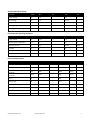
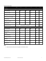
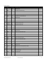
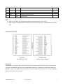
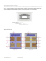
CPAC-‐TR-‐40SR-‐SSM160-‐QSFP-‐AO CHECKPOINT 40GBASE-‐SR4 QSFP+ MMF 850NM 150M REACH MPO DOM www.addoncomputer.com CPAC-‐TR-‐40SR-‐SSM160-‐QSFP-‐AO 40Gbase QSFP+ Transceiver Features • • • • • • • • • • • • • • Four-‐Channel full-‐duplex transceiver modules Transmission data rate up to 14.025Gbit/s per channel 4 channels 850nm VCSEL array 4 channels PIN photo detector array Low power consumption <1.5W Housing isolated from connector ground Operating case temperature 0°C to +70°C 3.3V power supply voltage RoHS 6 compliant Hot Pluggable QSFP form factor Maximum link length of 100m on OM3 Multimode Fiber (MMF) and 150m on OM4 MMF Single MPO connector receptacle Built-‐in digital diagnostic function Digital diagnostic compatible with SFF-‐847 Rev11.0 Applications • InfiniBand FDR • 16x Fibre Channel • PCI-‐e3.0 • Proprietary High Speed Interconnections • SAS 3.0 Product Description AddOn Computer’s CPAC-‐TR-‐40SR-‐SSM160-‐QSFP-‐AO Quad Small Form Factor Pluggable (QSFP+) transceivers are compatible with the Small Form Factor Pluggable Multi-‐Sourcing Agreement (MSA). The QSFP+ transceivers are high performance, cost effective modules supporting 40 Gigabit Ethernet and up to 150m transmission distance with MMF. AddOn Computer’s QSFP+ transceivers are RoHS compliant and lead-‐free. www.addoncomputer.com Phone: 877.292.1701 1 Absolute Maximum Ratings Parameter Symbol Min. Typ. Max. Unit Supply Voltage Vcc -‐0.3 3.6 V Input Voltage Vin -‐0.3 Vcc+0.3 V Storage Temperature Tst -‐20 85 °C Case Operating Temperature Top 0 70 °C Humidity (non-‐condensing) Rh 5 95 % Recommended Operating Conditions Parameter Symbol Min. Typ. Max. Unit Supply Voltage Vcc 3.13 3.3 3.47 V Operating Case Temperature Tca 0 70 °C Data Rate Per Lane fd 2.5 14.025 Gbps Humidity Rh 5 85 % Power Dissipation Pm 1.5 W Fiber Bend Radius Rb 3 cm Parameter Symbol Min. Typ. Max. Unit Notes Differential Input impedance Zin 90 100 110 ohm Differential Output impedance Zout 90 100 110 ohm ΔVin 300 1100 mVp-‐p ΔVout 500 800 mVp-‐p Skew Sw 300 ps Bit Error Rate BR E-‐12 Input Logic Level High VIH 2.0 VCC V Input Logic Level Low VIL 0 0.8 V Output Logic Level High VOH VCC-‐0.5 VCC V Output Logic Level Low VOL 0 0.4 V Electrical Characteristics Differential Input Voltage amplitude Differential output voltage amplitude www.addoncomputer.com Phone: 877.292.1701 2 Optical Characteristics Parameter Symbol Min. Typ. Max. Unit Notes Transmitter Center Wavelength λC 840 850 860 nm RMS Spectral Width ∆λ 0.65 nm Average Optical Power per Channel Pout -‐7.5 2.5 dBm Difference in launch power between any two lanes (OMA) 4 dB Extinction Ratio ER 3 dB Peak power, each lane 4 dBm Transmitter and dispersion penalty (TDP), each lane TDP 3.5 dB Hit Ratio = 5x10-‐5 Eye Mask Coordinates: X1, X2, X3, Y1, Y2, Y3 Specification Values 0.23, 0.34, 0.43, 0.27, 0.35, 0.4 Receiver Center Wavelength λC 840 850 860 nm Stressed receiver sensitivity in OMA, each lane -‐5.4 dBm 1 Average power at receiver input, each lane -‐9.5 2.4 dBm Receiver Reflectance -‐12 dB Peak power, each lane 4 dBm LOS Assert -‐30 dBm LOS De-‐Assert -‐ OMA -‐7.5 dBm LOS Hysteresis 0.5 dB Note: 1. Measured with conformance test signal at TP3 for BER = 10e-‐12 www.addoncomputer.com Phone: 877.292.1701 3 Pin Descriptions Pin Logic Symbol Name/Descriptions Ref. 1 GND Module Ground 1 2 CML-‐I Tx2-‐ Transmitter inverted data input 3 CML-‐I Tx2+ Transmitter non-‐inverted data input 4 GND Module Ground 1 5 CML-‐I Tx4-‐ Transmitter inverted data input 6 CML-‐I Tx4+ Transmitter non-‐inverted data input 7 GND Module Ground 1 8 LVTTL-‐I MODSEIL Module Select 2 9 LVTTL-‐I ResetL Module Reset 2 10 VCCRx +3.3v Receiver Power Supply 11 LVCMOS-‐I SCL 2-‐wire Serial interface clock 2 12 LVCMOS-‐I/O SDA 2-‐wire Serial interface data 2 13 GND Module Ground 1 14 CML-‐O RX3+ Receiver non-‐inverted data output 15 CML-‐O RX3-‐ Receiver inverted dta output 16 GND Module Ground 1 17 CML-‐O RX1+ Receiver non-‐inverted data output 18 CML-‐O RX1-‐ Receiver inverted data output 19 GND Module Ground 1 20 GND Module Ground 1 21 CML-‐O RX2-‐ Receiver inverted data output 22 CML-‐O RX2+ Receiver non-‐inverted data output 23 GND Module Ground 1 24 CML-‐O RX4-‐ Receiver inverted data output 25 CML-‐O RX4+ Receiver non-‐inverted data output 26 GND Module Ground 1 27 LVTTL-‐O ModPrsL Module Present, internal pulled down to GND 28 LVTTL-‐O IntL Interrupt output, should be pulled up on host board 2 29 VCCTx +3.3v Transmitter Power Supply 30 VCC1 +3.3v Power Supply 31 LVTTL-‐I LPMode Low Power Mode 2 32 GND Module Ground 1 33 CML-‐I Tx3+ Transmitter non-‐inverted data input www.addoncomputer.com Phone: 877.292.1701 4 34 CML-‐I Tx3-‐ Transmitter inverted data input 35 GND Module Ground 1 36 CML-‐I Tx1+ Transmitter non-‐inverted data input 37 CML-‐I Tx1-‐ Transmitter inverted data input 38 GND Module Ground 1 Note: 1. Module circuit ground is isolated from module chassis ground with in the module. 2. Open collector; should be pulled up with 4.7k-‐10k ohms on host board to a voltage between 3.15V and 3.6V. Electrical Pin-‐out Details ModSeIL Pin The ModSelL is an input pin. When held low by the host, the module responds to 2-‐wire serial communication commands. The ModSelL allows the use of multiple QSFP modules on a single 2-‐wire interface bus. When the ModSelL is “High”, the module will not respond to any 2-‐wire interface communication from the host. ModSelL has an internal pull-‐up in the module. www.addoncomputer.com Phone: 877.292.1701 5 ResetL Pin Reset. LPMode_Reset has an internal pull-‐up in the module. A low level on the ResetL pin for longer than the minimum pulse length (t_Reset_init) initiates a complete module reset, returning all user module settings to their default state. Module Reset Assert Time (t_init) starts on the rising edge after the low level on the ResetL pin is released. During the execution of a reset (t_init) the host shall disregard all status bits until the module indicates a completion of the reset interrupt. The module indicates this by posting an IntL signal with the Data_Not_Ready bit negated. Note that on power up (including hot insertion) the module will post this completion of reset interrupt without requiring a reset. LPMode Pin Operate in the low power mode (less than 1.5 W power consumption) This pin active high will decrease power consumption to less than 1W. ModPrsL Pin ModPrsL is pulled up to Vcc on the host board and grounded in the module. The ModPrsL is asserted “Low” when the module is inserted and de-‐asserted “High” when the module is physically absent from the host connector. IntL Pin IntL is an output pin. When “Low”, it indicates a possible module operational fault or a status critical to the host system. The host identifies the source of the interrupt by using the 2-‐wire serial interface. The IntL pin is an open collector output and must be pulled up to Vcc on the host board. Power Supply Filtering The host board should use the power supply filtering shown below. www.addoncomputer.com Phone: 877.292.1701 6 Optical Interface Lanes and Assignment The optical interface port is a male MPO connector .The four fiber positions on the left as shown below, with the key up, are used for the optical transmit signals (Channel 1 through 4). The fiber positions on the right are used for the optical receive signals (Channel 4 through 1). The central four fibers are physically present. Module Block Diagram www.addoncomputer.com Phone: 877.292.1701 7 Mechanical Specifications Contact Information AddOn Computer, Inc. is a leading supplier of Memory Upgrade, Network Transceivers and Network connectivity products to Channel Partners, Resellers and OEMs, with more than seventeen years of direct industry experience. AddOn Computer has been the exclusive supplier to Ingram Micro's "Memory Upgrades" program for the past nine years. AddOn Computer maximizes profitable opportunities for our partners. Our ability to source product worldwide, ensures that our pricing will always be competitive. Offering turnkey solutions, AddOn Computer has forged a reputation as a solutions provider, delivering high quality, cost effective product in a timely and reliable manner. Corporate office: AddOn Computer 30400 Esperanza Rancho Santa Margarita, CA 92688 Tel: 877-‐292-‐1701 Fax: 949-‐266-‐9273 Email: [email protected] Email: [email protected] Web: http://www.addoncomputer.com www.addoncomputer.com Phone: 877.292.1701 8