1
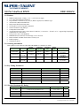
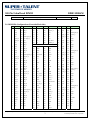
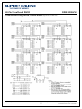
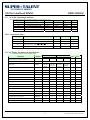
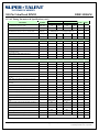
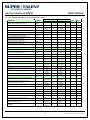
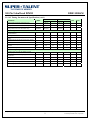
240-Pin Unbuffered DIMM
DDR3 SDRAM
DDR3 Unbuffered DIMM Module
2GB based on 1Gbit component
TFBGA with Pb-Free
Revision 1.01 (June.2009)
http://www.supertalent.com/oem
Products and Specifications discussed herein are subject to change without notice
1
© 2006 Super Talent Tech., Corporation.
240-Pin Unbuffered DIMM
DDR3 SDRAM
1.0 Features
•
•
•
•
•
•
•
•
•
•
•
•
•
•
JEDEC standard VDD = VDDQ = 1.5V +/- 0.075V Power Supply
1.5V centered-terminated push-pull I/O
Programmable CAS latencies (5,6,7,8,9,10), Burst Length (4 & 8) and Burst Type
Auto Refresh (CRB) and Self Refresh
Bi-directional Differential Data Strobe
Off Chip Driver (OCD) impedance adjustment
On-Die termination using ODT pin
8 independent internal bank
Average Refresh Period 7.8us at lower than a TCASE 85°C, 3.9us at 85°C < TCASE < 95 °C - support High Temperature
Self-Refresh rate enable feature
Serial presence detect with EEPROM
DIMM Dimension (Nominal) 30.00 mm high, 133.35 mm wide
Based on JEDEC standard reference Raw Cards Lay out.
RoHS compliant
Gold plated contacts
2.0 Ordering Information
These products can be ordered as individual 2GB DIMMs or as 4GB kits (2x 2GB).
Part number*
Density
Module
Organization
Component
composition
Component
PKG
Module
Rank
W1066UB2Gx
2GB
256Mx64
128Mx8*16
TFBGA
2
W1066UX4Gx
4GB Kit
(2x 2GB)
2x 256Mx64
128Mx8*16
TFBGA
2
W1333UB2Gx
2GB
256Mx64
128Mx8*16
TFBGA
2
W1333UX4Gx
4GB Kit
(2x 2GB)
2x 256Mx64
128Mx8*16
TFBGA
2
Description
2GB 2Rx8
PC3-8500U
2GB 2Rx8
PC3-8500U
2GB 2Rx8
PC3-10600U
2GB 2Rx8
PC3-10600U
*Last digit of part number indicates DRAM chip brand: E = Elpida; M = Micron; Q = Qimonda; S = Samsung.
3.0 Key Timing Parameters
CL-tRCD-tRP
DDR3-1333
9-9-9
DD3-1066
7-7-7
Unit
tCK
CAS Latency
tCK(min)
9
1.5
7
1.875
tCK
ns
13.125
13.125
ns
ns
37.5
50.625
ns
ns
tRCD(min)
tRP(min)
13.5
tRAS(min)
tRC(min)
36
13.5
49.5
4.0 Absolute Maximum DC Rating
Symbol
Parameter
Rating
Units
Vin , Vout
Voltage on any pin relative to VSS
-0.4 ~ 1.975
V
VDD
VDDQ
VDDL
Voltage on VDD & VDDQ supply relative to Vss
Short circuit current
Power dissipation
-0.4 ~ 1.975
-0.4 ~ 1.975
-0.4 ~ 1.975
V
V
V
http://www.supertalent.com/oem
Products and Specifications discussed herein are subject to change without notice
2
© 2006 Super Talent Tech., Corporation.
240-Pin Unbuffered DIMM
TSTG
DDR3 SDRAM
Storage Temperature
-55 ~ + 100
°C
5.0 DIMM Pin Configurations (Front side/Back side)
Pin
Front
Pin
Back
Pin
Front
Pin
Back
Pin
Front
Pin
Back
1
VREFDQ
121
Vss
41
Vss
161
DM8/DQS17_P
81
DQ32
201
DQ37
2
Vss
122
DQ4
42
NC
162
DQS17_N
82
DQ33
202
Vss
3
DQ0
123
DQ5
43
NC
163
Vss
83
Vss
203
DM4/DQS13_P
4
DQ1
124
Vss
44
Vss
164
NC
84
DQS4_N
204
DQS13_N
5
Vss
125
DM0/DQS9_P
45
NC
165
NC
85
DQS4_P
205
Vss
6
DQS0_N
126
NC/DQS9_N
46
NC
166
Vss
86
Vss
206
DQ38
7
DQS0_P
127
Vss
47
Vss
167
NC/TEST
87
DQ34
207
DQ39
48
NC
168
RESET_N
88
DQ35
208
Vss
89
Vss
209
DQ44
8
Vss
128
DQ6
9
DQ2
129
DQ7
KEY
10
DQ3
130
Vss
49
NC
169
CKE1
90
DQ40
210
DQ45
11
Vss
131
DQ12
50
CKE0
170
VDD
91
DQ41
211
Vss
12
DQ8
132
DQ13
51
VDD
171
A15
92
Vss
212
DM5/DQS14_P
13
DQ9
133
Vss
52
BA2
172
A14
93
DQS5_N
213
DQS14_N
14
Vss
134
DM1/DQS10_P
53
NC/Err-Out
173
VDD
94
DQS5_P
214
Vss
15
DQS1_N
135
DQS10_N
54
VDD
174
A12
95
Vss
215
DQ46
16
DQS2_P
136
Vss
55
A11
175
A9
96
DQ42
216
DQ47
17
Vss
137
DQ14
56
A7
176
VDD
97
DQ43
217
Vss
18
DQ10
138
DQ15
57
VDD
177
A8
98
Vss
218
DQ52
19
DQ11
139
Vss
58
A5
178
A6
99
DQ48
219
DQ53
20
Vss
140
DQ20
59
A4
179
VDD
100
DQ49
220
Vss
21
DQ16
141
DQ21
60
VDD
180
A3
101
VSS
221
DM6_DQS15_P
22
DQ17
142
Vss
61
A2
181
A1
102
DQS6_N
222
DQS15_N
23
Vss
143
DQS11_P
62
VDD
182
VDD
103
DQS6_P
223
Vss
24
DQS2_N
144
DQS11_N
63
CK1_P/NC
183
VDD
104
Vss
224
DQ54
25
DQS2_P
145
Vss
64
CK1_N/NC
184
CK0_P
105
DQ50
225
DQ55
Vss
26
Vss
146
DQ22
65
VDD
185
CK0_N
106
DQ51
226
27
DQ18
147
DQ23
66
VDD
186
VDD
107
Vss
227
DQ60
28
DQ19
148
Vss
67
VREFCA
187
NC/EVENT
108
DQ56
228
DQ61
29
Vss
149
DQ28
68
NC, Par_In
188
A0
109
DQ57
229
Vss
30
DQ24
150
DQ29
69
VDD
189
VDD
110
Vss
230
DM7/DQS16_P
31
DQ25
151
Vss
70
A10/AP
190
BA1
111
DQS7_N
231
DQS16_N
32
Vss
152
DM3/DQS12_P
71
BA0
191
VDD
112
DQS7_P
232
Vss
33
DQ3_N
153
DQS12_N
72
VDD
192
RAS_N
113
Vss
233
DQ62
34
DQ3_P
154
Vss
73
WE
193
S0_N
114
DQ58
234
DQ63
35
Vss
155
DQ30
74
CAS
194
VDD
115
DQ59
235
Vss
36
DQ26
156
DQ31
75
VDD
195
ODT0
116
Vss
236
VDDSPD
37
DQ27
157
Vss
76
S1
196
A13
117
SA0
237
SA1
38
Vss
158
NC
77
ODT1
197
VDD
118
SCL
238
SDA
39
NC
159
NC
78
VDD
198
NC
119
SA2
239
Vss
40
NC
160
Vss
79
S2/NC
199
Vss
120
VTT
240
VTT
80
Vss
200
DQ36
http://www.supertalent.com/oem
Products and Specifications discussed herein are subject to change without notice
3
© 2006 Super Talent Tech., Corporation.
240-Pin Unbuffered DIMM
DDR3 SDRAM
NC = No Connect, RFU = Reserved for Future Use
1. Par_in and Err_out pins are intended for register control functions.
6.0 DIMM Pin Description
Pin Name
Function
Pin Name
Function
A0 ~ A15
Address input (Multiplexed)
ODT0~ODT1
On Die Termination
A10/AP
Address Input/Auto pre-charge
CB0~CB7
ECC Data check bits Input/Output
BA0 ~ BA2
Bank Select
DQ0~DQ63
Data Input/Output
CK0 ~ CK2, CK0~CK2
Clock input
DQS0~DQS8
Data strobes, negative line
CKE0, CKE1
Clock enable input
DM (0~8),
Data Masks/Data strobes (Read)
S0, S1
Chip select input
DQS0~DQS8
Data Strobes
RAS
Row address strobe
RFU
Reserved for future used
CAS
Column address strobe
VTT
SDRAM I/O termination power supply
WE
Write Enable
TEST
Memory bus test tool
SCL
SPD Clock Input
VDD
Core Power
SDA
SPD Data Input/Output
VDDQ
I/O Power
SA0~SA2
SPD Address
VSS
Ground
VREFDQ
SDRAM Input/Output Reference Supply
VDDSPD
Serial EEPROM Power Supply
VREFCA
Command Address Reference Supply
Par_In
Err_Out
RESET
Parity bit for address & Control
bus
Parity error found in the
Address and Control bus
Register and PLL control pin
7.0 Address Configuration
Organization
Row Address
Column Address
Bank Address
Auto Pre-charge
128Mx8(1Gb) base
A0-A13
A0-A9
BA0-BA2
A10/AP
http://www.supertalent.com/oem
Products and Specifications discussed herein are subject to change without notice
4
© 2006 Super Talent Tech., Corporation.
240-Pin Unbuffered DIMM
DDR3 SDRAM
8.0 Functional Block Diagram: 2GB, 256Mx64 Module (Populated as 2 ranks of x8)
http://www.supertalent.com/oem
Products and Specifications discussed herein are subject to change without notice
5
© 2006 Super Talent Tech., Corporation.
240-Pin Unbuffered DIMM
DDR3 SDRAM
9.0 AC & DC Operating Conditions
Recommended operating conditions (Voltage referenced to Vss=0V, TA=0 to 70°C)
Symbol
Parameter
Min
Typ
Max
Unit
VDD
VDDQ
VREFDQ(DC)
VREFCA(DC)
VTT
Supply Voltage
Supply Voltage for Output
I/O Reference Voltage (DQ)
I/O Reference Voltage (CMD/Add)
Termination Voltage
1.425
1.425
0.49*VDDQ
0.49*VDDQ
0.49*VDDQ
1.5
1.5
0.50*VDDQ
0.50*VDDQ
0.50*VDDQ
1.575
1.575
0.51*VDDQ
0.51*VDDQ
0.51*VDDQ
V
V
V
V
V
10.0 Capacitance (Max.)
Symbol
CCK
CI1
CI2
CIO
Parameter/Condition
Min
Max
Unit
11
pF
12
pF
12
pF
10
pF
-
Input capacitance, CK and CK
-
Input capacitance, CKE and CS
-
Input capacitance, Addr, RAS, CAS, WE
-
Input capacitance, DQ, DM, DQS, DQS
11.1 AC Timing Parameters & Specifications
(AC operating conditions unless otherwise noted)
Parameter
Symbol
Minimum Clock Cycle Time (DLL off mode)
tCK(DLL_OFF)
Average Clock Period
tCK(avg)
Clock Period
tCK(abs)
DDR3-1066
DDR3-1333
min
min
max
8
-
Units
max
8
-
See Speed Bins Table
tCK(avg)
min +tJIT
tCK(avg)
min +tJIT
(per)min
tCK(avg)
max +tJIT
(per)max
ns
6
ps
ps
(per)min
tCK(avg)
max +tJIT
(per)max
Average high pulse width
tCH(avg)
0.47
0.53
0.47
0.53
tCK(avg)
Average low pulse width
tCL(avg)
0.47
0.53
0.47
0.53
tCK(avg)
Clock Period Jitter
tJIT(per)
-90
90
-80
80
ps
Clock Period Jitter during DLL locking period
tJIT(per, lck)
-90
90
-80
80
ps
Cycle to Cycle Period Jitter
tJIT(cc)
180
160
ps
Cycle to Cycle Period Jitter during DLL locking period
tJIT(cc, lck)
160
140
ps
Cumulative error across 2 cycles
tERR(2per)
- 132
132
- 118
118
ps
Cumulative error across 3 cycles
tERR(3per)
- 157
157
- 140
140
ps
Cumulative error across 4 cycles
tERR(4per)
- 175
175
- 155
155
ps
Cumulative error across 5 cycles
tERR(5per)
- 188
-188
- 168
168
ps
Cumulative error across 6 cycles
tERR(6per)
- 200
200
- 177
177
ps
Cumulative error across 7 cycles
tERR(7per)
- 209
209
- 186
186
ps
Cumulative error across 8 cycles
tERR(8per)
- 217
217
- 193
193
ps
Cumulative error across 9 cycles
tERR(9per)
- 224
224
- 200
200
ps
Cumulative error across 10 cycles
tERR(10per)
- 231
231
- 205
205
ps
http://www.supertalent.com/oem
Notes
Products and Specifications discussed herein are subject to change without notice
6
© 2006 Super Talent Tech., Corporation.
240-Pin Unbuffered DIMM
DDR3 SDRAM
11.2 AC Timing Parameters & Specifications (con’t)
Parameter
Symbol
DDR3-1066
min
DDR3-1333
max
min
max
Units
Cumulative error across 11 cycles
tERR(11per)
- 237
237
- 210
210
ps
Cumulative error across 12 cycles
tERR(12per)
- 242
242
- 215
215
ps
Cumulative error across n = 13, 14 ... 49, 50 cycles
tERR(nper)
tERR(nper)min = (1 + 0.68ln(n))*tJIT(per)min
tERR(nper)max = (1 = 0.68ln(n))*tJIT(per)max
Absolute clock HIGH pulse width
tCH(abs)
0.43
-
0.43
Absolute clock Low pulse width
tCL(abs)
0.43
-
DQS, /DQS to DQ skew, per group, per access
tDQSQ
-
DQ output hold time from DQS, /DQS
tQH
DQ low-impedance time from CK, /CK
DQ high-impedance time from CK, /CK
Notes
ps
24
-
tCK(avg)
25
0.43
-
tCK(avg)
26
150
-
125
ps
13
0.38
-
0.38
-
tCK(avg)
13,g
tLZ(DQ)
-600
300
-500
250
ps
13,14,f
tHZ(DQ)
-
300
-
250
ps
13,14,f
tDS(base)
25
-
TBD
-
ps
d,17
tDH(base)
100
-
TBD
-
ps
d,17
tDIPW
490
-
400
-
ps
28
DQS, /DQS READ Preamble
tRPRE
0.9
Note 19
0.9
Note 19
tCK
13,19,g
DQS, /DQS differential READ Postamble
tRPST
0.3
Note 11
0.3
Note 11
tCK
11,13,g
DQS, /DQS output high time
tQSH
0.38
-
0.4
-
tCK(avg)
DQS, /DQS output low time
tQSL
0.38
-
0.4
-
tCK(avg)
Data Timing
Data setup time to DQS, /DQS referenced to
Vih(ac)Vil(ac) levels
Data hold time to DQS, /DQS referenced to
Vih(ac)Vil(ac) levels
DQ and DM Input pulse width for each input
Data Strobe Timing
DQS, /DQS WRITE Preamble
tWPRE
0.9
-
0.9
-
tCK
DQS, /DQS WRITE Postamble
tWPST
0.3
-
0.3
-
tCK
tDQSCK
-300
300
-255
255
ps
13,f
tLZ(DQS)
-600
300
-500
250
ps
13,14,f
tHZ(DQS)
300
-
250
-
ps
12,13,14
DQS, DQS differential input low pulse width
tDQSL
0.45
0.55
0.45
0.55
tCK
28,30
DQS, DQS differential input high pulse width
tDQSH
0.45
0.55
0.45
0.55
tCK
29,30
DQS, DQS rising edge to CK, CK rising edge
tDQSS
-0.25
0.25
-0.25
0.25
tCK(avg)
C
DQS,DQS faling edge setup time to CK, CK rising edge
tDSS
0.2
-
0.2
-
tCK(avg)
C,31
DQS,DQS faling edge hold time to CK, CK rising edge
tDSH
0.2
-
0.2
-
tCK(avg)
C,31
DLL locking time
tDLLK
512
-
512
-
nCK
DQS, /DQS rising edge output access time from rising
CK, /CK
DQS, /DQS low-impedance time (Referenced from RL1)
DQS, /DQS high-impedance time (Referenced from
RL+BL/2)
internal READ Command to PRECHARGE Command
delay
Delay from start of internal write transaction to internal
read command
tRTP
tWTR
WRITE recovery time
tWR
Mode Register Set command cycle time
max
(4tCK,7.5ns)
max
(4tCK,7.5ns)
-
15
-
tMRD
4
Mode Register Set command update delay
tMOD
max
(12tCK,15ns)
CAS# to CAS# command delay
tCCD
4
Auto precharge write recovery + precharge time
tDAL(min)
http://www.supertalent.com/oem
max
(4tCK,7.5ns)
max
(4tCK,7.5ns)
-
e
-
e,18
15
-
ns
-
4
-
nCK
-
max
(12tCK,15ns)
-
-
4
-
WR + roundup (tRP / tCK(AVG))
e
nCK
nCK
Products and Specifications discussed herein are subject to change without notice
7
© 2006 Super Talent Tech., Corporation.
240-Pin Unbuffered DIMM
DDR3 SDRAM
11.3 AC Timing Parameters & Specifications (con’t)
Parameter
Symbol
Multi-Purpose Register Recovery Time
tMPRR
ACTIVE to PRECHARGE command period
tRAS
DDR3-1066
min
DDR3-1333
max
1
-
37.5
70,000
max
(4tCK,7.5ns)
max
(4tCK,10ns)
min
max
Units
1
-
nCK
36
70,000
ns
max
(4tCK,6ns)
max
(4tCK,7.5ns)
Notes
e
-
e
-
e
ACTIVE to ACTIVE command period for 1KB page size
tRRD
ACTIVE to ACTIVE command period for 2KB page size
tRRD
Four activate window for 1KB page size
tFAW
37.5
-
30
-
ns
e
Four activate window for 2KB page size
tFAW
50
-
45
-
ns
e
tIS(base)
125
-
65
-
ps
b,16
tIH(base)
200
-
140
-
ps
b,16
tIS(base)
AC150
-
-
65+125
-
ps
b,16,27
tIPW
780
-
620
-
ps
28
Power-up and RESET calibration time
tZQinitI
512
-
512
-
tCK
Normal operation Full calibration time
tZQoper
25
-
256
-
tCK
Normal operation short calibration time
tZQCS
64
-
64
-
tCK
max(5tCK,
tRFC+ 10ns)
-
max(5tCK,
tRFC+ 10ns)
-
max(5tCK,tRF
C+ 10ns)
-
max(5tCK,tRF
C+ 10ns)
-
tDLLK(min)
-
tDLLK(min)
-
Command and Address setup time to CK, CK
referenced to Vih(ac) / Vil(ac) levels
Command and Address hold time from CK, CK
referenced to Vih(ac) / Vil(ac) levels
Command and Address setup time to CK, CK
referenced to Vih(ac) / Vil(ac) levels
Control & Address Input pulse width for each input
-
Calibration Timing
23
Reset Timing
Exit Reset from CKE HIGH to a valid command
tXPR
Self Refresh Timing
Exit Self Refresh to commands not requiring a locked
DLL
tXS
Exit Self Refresh to commands requiring a locked DLL
tXSDLL
Minimum CKE low width for Self refresh entry to exit
timing
tCKESR
Valid Clock Requirement after Self Refresh Entry (SRE)
tCKSRE
Valid Clock Requirement before Self Refresh Exit (SRX)
tCKSRX
tCKE(min) +
1tCK
max(5tCK,
10ns)
max(5tCK,
10ns)
-
tCKE(min) +
1tCK
max(5tCK,
10ns)
max(5tCK,
10ns)
nCK
-
Power Down Timing
Exit Power Down with DLL on to any valid command;
Exit Precharge Power Down with DLL
frozen to commands not requiring a locked DLL
Exit Precharge Power Down with DLL frozen to
commands requiring a locked DLL
tXP
tXPDLL
CKE minimum pulse width
tCKE
Command pass disable delay
tCPDED
Power Down Entry to Exit Timing
tPD
Timing of ACT command to Power Down entry
tACTPDEN
max
(3tCK,7.5ns)
max(10tCK,
24ns)
max(3tCK,
5.625ns)
-
max
(3tCK,6ns)
max(10tCK,
24ns)
max(3tCK,
5.625ns)
-
1
-
1
-
nCK
tCKE(min)
9*tREFI
tCKE(min)
9*tREFI
tCK
15
1
-
1
-
nCK
20
nCK
20
-
nCK
9
-
nCK
10
-
nCK
9
Timing of PRE command to Power Down entry
tPRPDEN
1
-
1
-
Timing of RD/RDA command to Power Down entry
tRDPDEN
RL + 4 +1
-
RL + 4 +1
-
Timing of WR command to Power Down entry
(BL8OTF, BL8MRS, BL4OTF)
Timing of WRA command to Power Down entry
(BL8OTF, BL8MRS, BL4OTF)
Timing of WR command to Power Down entry
(BL4MRS)
http://www.supertalent.com/oem
tWRPDEN
tWRAPDEN
tWRPDEN
2
WL + 4
+(tWR/tCK)
WL + 4
+WR+1
WL + 2
+(tWR/
tCK(avg))
-
WL + 4
+(tWR/tCK)
WL + 4
+WR+1
WL + 2
+(tWR/
tCK(avg))
Products and Specifications discussed herein are subject to change without notice
8
© 2006 Super Talent Tech., Corporation.
240-Pin Unbuffered DIMM
DDR3 SDRAM
11.4 AC Timing Parameters & Specifications (con’t)
Parameter
Symbol
Timing of WRA command to Power Down entry
(BL4MRS)
tWRAPDEN
DDR3-1066
DDR3-1333
min
min
max
WL +2
+WR +1
-
Units
max
WL +2
+WR +1
-
Timing of REF command to Power Down entry
tREFPDEN
1
-
1
-
Timing of MRS command to Power Down entry
tMRSPDEN
tMOD(min)
-
tMOD(min)
-
nCK
Notes
10
20,21
ODT Timing
ODT high time without write command or with wirte
commandand BC4
ODTH4
4
-
4
-
nCK
ODT high time with Write command and BL8
ODTH8
6
-
6
-
nCK
tAONPD
1
9
1
9
ns
tAOFPD
1
9
1
9
ns
Asynchronous RTT tum-on delay (Power-Down with DLL
frozen)
Asynchronous RTT tum-off delay (Power-Down with DLL
frozen)
ODT turn-on
tAON
-300
300
-250
250
ps
7,f
RTT_NOM and RTT_WR turn-off time from ODTL off
reference
tAOF
0.3
0.7
0.3
0.7
tCK(avg)
8,f
RTT dynamic change skew
tADC
0.3
0.7
0.3
0.7
tCK(avg)
f
tWLMRD
40
-
40
-
tCK
3
tWLDQSEN
25
-
25
-
tCK
3
Setup time for tDQSS latch
tWLS
245
-
195
-
ps
Hold time of tDQSS latch
tWLH
245
-
195
-
ps
Write leveling output delay
tWLO
0
9
0
9
ns
Write leveling output error
tWLOE
0
2
0
2
ns
Write Leveling Timing
First DQS pulse rising edge after tDQSS margining
mode is programmed
DQS/DQS delay after tDQS margining mode is
programmed
http://www.supertalent.com/oem
Products and Specifications discussed herein are subject to change without notice
9
© 2006 Super Talent Tech., Corporation.
240-Pin Unbuffered DIMM
DDR3 SDRAM
12.0 Physical Dimensions: (128Mbx8 Based, 256Mx64, 2 ranks)
Tolerances :± 0.005(.13) unless otherwise specified
http://www.supertalent.com/oem
Products and Specifications discussed herein are subject to change without notice
10
© 2006 Super Talent Tech., Corporation.