1
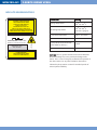
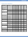
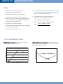
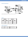
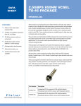
DATA
SHEET
2.5GBPS 850NM VCSEL
LC TOSA PACKAGE
HFE419X-441
FEATURES:
850nm multi-mode oxide
isolated VCSEL
Extended Temperature Range
Operation (– 40 to +85 deg
operating range)
Capable of modulation operation
from DC to 2.5Gbps
TO-46 tilt window metal can
component, prealigned into LC
Sleeve
Designed for drive currents
between 3-15mA average
Packaged with a back monitor
Attenuated window can
These products are high-performance 850nm VCSELs (Vertical Cavity SurfaceEmitting Lasers) designed for high-speed data communications and packaged
with a custom designed power monitor diode. The power monitor diode can
be used with appropriate feedback control circuitry to set a maximum power
level for the VCSEL. These combined features simplify design for high data rate
communication and eye safety.
These products are high radiance VCSELs designed to convert electrical current
into optical power that can be used in fiber optic communications and other
applications. As the current varies above threshold, the light intensity
increases proportionally.
These products are designed to be used with inexpensive silicon or gallium
arsenide detectors, but excellent performance can also be achieved with some
indium gallium arsenide detectors (see HFD3180-103 and HFD3180-108
product data sheets).
The low drive current requirement makes direct drive from PECL (Positive
Emitter Coupled Logic) or ECL (Emitter Coupled Logic) gates possible and eases
driver design.
VCSELs produce circularly symmetric, non-astigmatic, narrow divergence
beams that, with appropriate lensing, fiber couple all of the emitter power.
These LC TOSA products are pre-aligned and focused fiber optic transmitters
designed to interface with 50/125 and 62.5/125 µm multi-mode fiber.
Part Number
HFE4190-441
HFE4191-441
Description
LC TOSA with attenuated TO-46 component, VCSEL with Back Monitor
Photodiode, Anode of VCSEL common with Photodiode Cathode
LC TOSA with attenuated TO-46 component, VCSEL with Back Monitor
Photodiode, Cathode of VCSEL common with Photodiode Anode
HFE419X-441
2.5GBPS 850NM VCSEL
ABSOLUTE MAXIMUM RATINGS
INVISIBLE LASER RADIATION
AVOID EXPOSURE TO BEAM
CLASS 3B LASER PRODUCT
30mW at 820-860 nm
PER IEC/EN 60825-1/A2.2001
AND 21 CFR 1040.10 AND 1040.11
EXCEPT FOR DEVIATIONS PURSUANT TO
LASER NOTICE NO.50 DATED 26 JULY 2001
SEMICONDUCTOR LASER
Advanced Optical Components
600 Millennium Drive,
Allen, TX 75013
LASER RADIATION
AVOID EXPOSURE TO BEAM
CLASS 3B LASER PRODUCT
PN55449
AVOID EXPOSURE: Invisible LASER
radiation is emitted from this aperture.
Parameter
Rating
Storage temperature
-40oC to +85oC
Operating temperature
-40oC to +85oC,
See note 1 (page 3)
Lead solder temperature
260oC, 10 seconds
Laser continuous average current
12mA
Laser peak forward current with
pulse width less than 1µs
18mA
Laser reverse voltage
5V
NOTICE: Stresses greater than those listed under “Absolute
Maximum Ratings” may cause permanent damage to the
device. This is a stress rating only and functional operation of
the device at these or any other conditions above those
indicated in the operations section for extended periods of
time may affect reliability.
HFE419X-441
ELECTRICAL-OPTICAL CHARACTERISTICS
VCSEL Parameters
Test Condition
Average Fiber Coupled
Power
Minimum coupling
efficiency including
wiggle
Threshold Current
Threshold Current
maximum deviation from
25oC value
I F = 7mA
Temperature atminimum
threshold current
Slope Efficiency
Slope Efficiency
Temperature variation
Peak Wavelength
I F = 7mA
o
o
T A = 0 C to 70 C
T A = 25oC to 85 oC
T A = -40oC to 25 oC
T A = 25oC
T A = -40oC
T A = 85oC
T A = 0 oC to 70 oC
Photodiode Parameters
Test Condition
Relative Intensity Noise
Series Resistance
Monitor Current
Monitor current
Temperature Variation
Monitor Current Tracking
Dark Current
PD Capacitance
Typ.
Max.
Units
Notes
mW
2
%
2
2.5
1
1.7
2.5
50
mA
mA
mA
mA
o
C
3
3
3
3
0.16
0.200
mW/mA
mW/mA
mW/mA
ppm/oC
0.500
55
Series Resistance
Temperature Coefficient
Spectral Bandwidth, RMS
Laser Forward Voltage
Rise and Fall Times
Min.
P OC
I F = 7mA,
T A = 0oC to 85oC
I F = 7mA,
T A = -40oC to 85 oC
I F = 7mA
I F = 7mA
Pavg = 0.625mW,
E xtinction Ratio = 10
1 GHz BW, I F = 7mA
I F = 7mA , T A = 25oC
T A = -40oC
T A = 85oC
I F = 7mA,
T A = 0 oC to 70 oC
λ P Temperature Variation
Symbol
0.5
-0.5
η
η
η
∆η/∆T
0.04
λP
830
∆λ
VF
tr
tf
RIN
RS
RS
RS
-6000
850
860
1.8
25
-130
35
0.65
2.0
130
150
-122
50
60
I PD
I PD
I PD
∆I PD /∆T
0.1
TBD
TBD
nm
6
dB/Hz
Ω
Ω
Ω
ppm/oC
7
Max.
Units
Notes
0.6
TBD
TBD
mA
-3000
Typ.
TBD
mA
%/ oC
TBD
75
40
5
nm
V
ps
20
Min.
4
nm/oC
0.06
Symbol
Deltrk
ID
C
0.125
0.03
∆R s/∆T
Poc = 0.5mW, T A = 25 C
Poc = 0.5mW, T A = -40oC
Poc = 0.5mW, T A = +85oC
Poc = 0.5mW, 0 oC to 70 oC
1.8
-20
∆λ P/∆T
o
Po = 0mW, V R = 3V
V R = 0V, Freq = 1MHz
V R = 3V, Freq = 1MHz
I TH
∆I TH
∆I TH
∆I TH
TO
8
20
100
55
nA
pF
HFE419X-441
2.5GBPS 850NM VCSEL
NOTES
1.
Reliability is a function of temperature, see
www.finisar.com/aoc.php for details.
2.
For the purpose of these tests, IF is DC current.
3.
Threshold current varies as (TA – TO)2. It may either
increase or decrease with temperature, depending upon
relationship of TA to TO. The magnitude of the change is
proportional to the threshold at TO.
4.
Slope efficiency is defined as ∆PO/∆IF.
5.
To compute the value of Slope Efficiency at a temperature
T, use the following equation:
6.
Rise and fall times specifications are the 20% - 80%. Most
of the devices will measure <135ps fall time. Rise and fall
times are sensitive to drive electronics..
7
To compute the value of Series Resistance at a
temperature T, use the following equation:
RS(T) ≈ RS(25oC)*[1+∆RS/∆T)*(T-25)]
8.
Monitor current tracking is defined as follows:
Deltrk =
IPD(PO = 0.75mW) / 0.75mW
IPD(PO = 0.45mW) / 0.45mW
η(T) ≈ η(25oC)*[1+(∆η/∆T)*(T-25)]
TYPICAL PERFORMANCE CURVES
Pmax
Emitted Power
η
Typical operating current / power
I th
Current
Threshold Current vs. Temperature: Threshold current varies
parabolically with temperature; thus it can be nearly constant
for a limited temperature range.
Threshold Current
Emitted Power vs. Current: Power varies approximately
linearly with current above threshold.
I TH
-4
2
IMIN [1.1×10 (T-TMIN ) +1]
TMIN , I MIN
Temperature
HFE419X-441
MOUNTING DIMENSIONS
MOUNTING DIMENSIONS (for reference only): All dimensions are in inches.
PINOUT
HFE4190-441
Number
HFE4191-441
Function
Number
Function
1
KLD
1
ALD
2
KPD, ALD
2
KLD, APD
3
APD
3
KPD
PINOUT DEFINITIONS
ALD
VCSEL Anode
APD
Monitor Photodiode Anode
KLD
VCSEL Cathode
KPD
Monitor Photodiode Cathode
HFE419X-441
2.5GBPS 850NM VCSEL
ADVANCED OPTICAL COMPONENTS
AOC CAPABILITIES
Finisar’s ADVANCED OPTICAL COMPONENTS division was
formed through strategic acquisition of key optical component suppliers. The company has led the industry in high
volume Vertical Cavity Surface Emitting Laser (VCSEL) and
associated detector technology since 1996. VCSELs have
become the primary laser source for optical data communication, and are rapidly expanding into a wide variety of sensor
applications. VCSELs’ superior reliability, low drive current,
high coupled power, narrow and circularly symmetric beam
and versatile packaging options (including arrays) are enabling
solutions not possible with other optical technologies.
ADVANCED OPTICAL COMPONENTS is also a key supplier of
Fabrey-Perot (FP) and Distributed Feedback (DFB) Lasers, and
Optical Isolators (OI) for use in single mode fiber data and
telecommunications networks
ADVANCED OPTICAL COMPONENTS’ advanced capabilities
include:
1, 2, 4, 8, and 10Gbps serial VCSEL solutions
1, 2, 4, 8, and 10Gbps serial SW DETECTOR solutions
VCSEL and detector arrays
1, 2, 4, 8, and 10Gbps FP and DFB solutions at 1310 and
1550nm
1, 2, 4, 8, and 10Gbps serial LW DETECTOR solutions
Optical Isolators from 1260 to 1600nm range
Laser packaging in TO46, TO56, and Optical
subassemblies with SC, LC, and MU interfaces for
communication networks
VCSELs operating at 670nm, 780nm, 980nm, and 1310nm
in development
LOCATION
Allen, TX - Business unit headquarters, VCSEL wafer
growth, wafer fabrication and TO package assembly.
Fremont, CA – Wafer growth and fabrication of 1310 to
1550nm FP and DFB lasers.
Sensor packages include surface mount, various plastics,
chip on board, chipscale packages, etc.
Custom packaging options
Shanghai, PRC – Optical passives assembly, including
optical isolators and splitters.
SALES AND SERVICE
Finisar’s ADVANCED OPTICAL COMPONENTS division serves its
customers through a worldwide network of sales offices and
distributors. For application assistance, current specifications,
pricing or name of the nearest Authorized Distributor, contact
a nearby sales office or call the number listed below.
Phone:1-866-MY-VCSEL USA (toll free)
1-214-509-2700 USA (Direct dial)
44 (0) 174 336 5533 Europe
886-935-409898 China & Taiwan
81-90-4437-1130 Japan
82-11-220-6153 Asia Pacific & Korea
Fax: 1-214-509-3709 USA
Email: [email protected]
WEB: www.finisar.com/aoc.php
©2007 Finisar Corporation. All rights reserved. Finisar is a registered trademark of Finisar Corporation. Features and specifications are subject to change without notice.
1/07