1
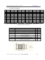
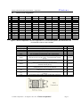
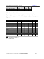
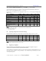
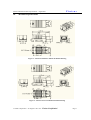
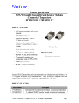
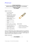
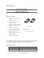
Finisar Product Specification SNAP12 Parallel Transmitter and Receiver Modules Industrial Temperature FTXD02SL1T / FRXD02SL1T PRODUCT FEATURES • 12-channel transmitter and receiver modules • SNAP12 form factor • Multirate capability: 1Gb/s to 2.7Gb/s per channel • Maximum link length of 600m at 2.5Gb/s on OM3 Multimode Fiber (MMF) Product Photo • Unretimed electrical interface • 3.3V power supply required • Reliable VCSEL array technology • Industrial operating case temperature range of -40ºC to 85ºC • MPO type connector • RoHS-6 compliant (lead-free) APPLICATIONS • Interchassis connections Finisar’s SNAP12 transmitter and receiver modules are designed to be used in links of up to 32 Gigabit per second over multimode fiber. They are RoHS-6 compliant and leadfree per Directive 2002/95/EC1, and Finisar Application Note AN-20382 PRODUCT SELECTION Part Number Description FTXD02SL1T 12-channel SNAP12 transmitter module FRXD02SL1T 12-channel SNAP12 receiver module Finisar Corporation – 26-August-11 Rev A4 – Finisar Confidential Page 1 Finisar SNAP12 Modules Product Specification – August 2011 I. Transmitter Pin Assignment K J H G F E D C B A NIC NIC NIC GND GND GND GND GND GND NIC 2 NIC NIC NIC NIC NIC GND GND DIN6P GND GND DIN9P GND 3 NIC NIC VCC VCC GND DIN5P DIN6N GND DIN8P DIN9N GND 4 NIC NIC VCC VCC DIN4P DIN5N GND DIN7P DIN8N GND NIC 5 NIC NIC VCC VCC VCC VCC DIN4N GND DIN3P DIN7N GND DIN10n GND 6 NIC VCC VCC GND DIN2P DIN3N GND DIN11n DIN10p GND 7 NIC NIC NIC NIC DIN1P DIN2N GND DIN12n DIN11p GND NIC 8 NIC NIC RESET- FAULT- DIN1N GND GND DIN12p GND GND NIC 9 NIC NIC TXEN TXDIS GND GND GND GND GND GND NIC NIC 10 NIC NIC SDA SCL NIC NIC NIC NIC NIC NIC NIC 1 Figure 1 – Transmitter 100pin MSA connector assignments as viewed from the topside of the customer line card (Toward MPO connector end of module) Signal Name Din[12:1]P Din[12:1]N NIC GND ResetFAULT– TXDIS TXEN SDA SCL Vcc Signal Description Transmitter Data Non-inverting Input for channels 11 through 0 Transmitter Data Inverting Input for channels 11 through 0 Reserved – Do Not Connect to any voltage on Host PCB Signal Common ground Reset signal to module, Asserted Low. Internal pullup. Transmitter Fault indicator. Logical Low indicates fault Laser disable; LOW = normal operation if TXEN normal; HIGH = lasers off; internal pull-down, Laser enable; HIGH = normal operation if TXDIS normal; LOW = lasers off; internal pull-up. I2C data signal, internal pull-up with a 10 kΩ resistor. I2C clock signal. Internal pull-up with a 10kΩ resistor. 3.3 V Power supply, external common connection of pins required – not common internally Finisar Corporation – 26-August-11 Rev A4 – Finisar Confidential I/O I I Type CML CML I O I LVTTL I LVTTL I/O I Page 2 Finisar SNAP12 Modules Product Specification – August 2011 II. Receiver Pin Assignment K J H G F E D C B A Vpp NIC NIC GND GND GND GND GND GND NIC 2 Vpp NIC NIC NIC NIC GND GND DOUT6N GND GND DOUT9N GND 3 NIC NIC VCC VCC GND DOUT5N DOUT6P GND DOUT8N DOUT9P GND 4 NIC NIC VCC VCC DOUT4N DOUT5P GND DOUT7N DOUT8P GND NIC 5 NIC NIC VCC VCC VCC VCC DOUT4P GND DOUT3N DOUT7P GND DOUT10p GND 6 NIC VCC VCC GND DOUT2N DOUT3P GND DOUT11p DOUT10n GND 7 NIC NIC NIC SD DOUT1N DOUT2P GND DOUT12p DOUT11n GND NIC 8 NIC Vpp -SD12 SD1 DOUT1P GND GND DOUT12n GND GND NIC 9 NIC Vpp RXEN ENSD GND GND GND GND GND GND NIC NIC 10 NIC SQEN SDA SCL NIC NIC NIC NIC NIC NIC NIC 1 Figure 2 – Receiver 100pin MSA connector assignments as viewed from the topside of the customer line card (Toward MPO connector end of module) Signal Name DOUT[12:1]P DOUT[12:1]N NIC GND SDA SCL SQEN ENSD RXEN SD SD1 Vcc Vpp Signal Description Receiver Data Non-inverting Input for channels 11 through 0 Receiver Data Inverting Input for channels 11 through 0 Reserved – Do Not Connect to any voltage on Host PCB Signal Common ground I2C data signal. Internal pull-up with a 10 kΩ resistor. I2C clock signal. Internal pull-up with a 10 kΩ resistor. Squelch enable; HIGH = all data outputs driven to logic zero when SD is active (LOW); LOW = squelch disabled; internal pull-up Signal detect enable; HIGH = normal operation; LOW = signal detect output(s) forced active; internal pull-up Output enable; HIGH = normal operation; LOW = receiver disabled; internal pull-up Global signal detect; HIGH = normal operation; LOW = inadequate power on one or more channels Signal detect channel 1; HIGH = normal operation; LOW = inadequate power on channel 1 3.3 V Power supply, external common connection of pins required Not required on this product. Pads not internally connected. Finisar Corporation – 26-August-11 Rev A4 – Finisar Confidential I/O I I Type CML CML I/O I I LVTTL I LVTTL I LVTTL O LVTTL O LVTTL I I Page 3 Finisar SNAP12 Modules Product Specification – August 2011 III. Absolute Maximum Ratings The following table represents the absolute maximum ratings for the SNAP12 transmitter and receiver modules. Absolute maximum is defined as the maximum point of exertion without permanent damage to the SNAP12 modules. Parameter Storage case temperature range Symbol TS Static discharge voltage Min -40 ESD Max 85 Unit o C Ref. 1 500 V 2 Relative humidity (non-condensing) RH 5 95 % Supply voltage VCC -0.5 +3.6 V Notes: 1. Operation guaranteed for bit rates up to 2.7 Gbps. 2. Human Body Model (HBM). IV. Power Supply Information Parameter Symbol Vcc Supply voltage Steady supply current Min 3.13 Typ 3.30 Max 3.47 Unit V Ref. 1, 2 Transmitter module ICC 350 420 mA 1, 2 Receiver module ICC 400 450 mA 1, 2 Notes: 1. Performance will be guaranteed as long as the supply voltage range is within the defined parameters. V. Transmission Specification Parameter Transmitter (per channel) Bit rate Min 1 Typ 2.5 Max 2.7 Unit Gbps 1 2.5 2.7 Gbps 500 MHz·km 50µm MMF 300 m 1 2000 MHz·km 50µm MMF 600 m 1 Receiver (per channel) Fiber link length @2.5Gbps Ref. Notes: 1. BER<1e-12, PRBS 2^23-1. VI. Control and Status Signal Level Specification Parameter Input voltage - logic LOW Min -50 Input voltage - logic HIGH 2000 Input current Typ Max 800 Unit mV Vcc mV 125 µA Finisar Corporation – 26-August-11 Rev A4 – Finisar Confidential Page 4 Finisar SNAP12 Modules Product Specification – August 2011 Output voltage - logic LOW GND 400 mV Output voltage - logic HIGH 2400 VCC mV 10 µA Output current high resistance VII. Trasmitter Module Performance (TOP = -40 to 85°°C, VCC = 3.3 ± 5% Volts) The following characteristics are defined over the Recommended Operating Conditions of 40°C to +85°C case temperature and Vcc = 3.3V ±5%. Typical values are defined at a case temperature of 40˚C, Vcc = 3.3V, bit rate of 2.5Gbps with PRBS 2^23-1 Parameter Optical Interface Characteristics Connector type Center wavelength range Symbol Min Typ Unit 860 nm 0.85 nm -2 dBm -30 dBm Ref. MPO λ 830 Spectral width (rms) Output power average (per channel) Output power average (per channel) with Tx Disable asserted Extinction ratio Optical Modulation Amplitude (OMA) Accumulated deterministic jitter Max PO AV ER Accumulated total jitter High-Speed Electrical Interface Characteristics Differential input swing (P-P) Vin,pp Input termination resistance, differential -8 6 dB -7.2 dBm 200 80 100 1 60 ps 120 ps 1900 mV 1 120 ohm 2 Notes: 1. At 2.5Gbps, BER=1E-12, PRBS 2^23-1. 2. DC-coupled internally. Finisar Corporation – 26-August-11 Rev A4 – Finisar Confidential Page 5 Finisar SNAP12 Modules Product Specification – August 2011 VIII. Receiver Module Performance (TOP = -40 to 85°°C, VCC33 = 3.3 ± 5% Volts) The following characteristics are defined over the Recommended Operating Conditions of 40°C to +85°C case temperature and Vcc = 3.3V ±5%. Typical values are defined at a case temperature of 40˚C, Vcc = 3.3V, bit rate of 2.5Gbps with PRBS 2^23-1 Parameter Symbol Optical Interface Characteristics Connector type Wavelength range λ Input optical power sensitivity Pin min Return loss Overload Pin max LOS De-Assert LOS Assert LOS Hysteresis High-Speed Electrical Interface Characteristics Differential output swing (P-P) Vout,pp Output termination resistance, differential Min Typ Max Unit Ref. 860 -16 nm dBm dB dBm dBm dBm dB 670 mV 2 120 ohm 3 MPO 830 -18 12 -2 -21 -23 2.5 500 80 100 1 Notes: 1. 2.5Gbps, BER=1E-12, PRBS 2^23-1 with Extinction Ratio of 6dB minimum. 2. BER=1E-12, PRBS 2^23-1. 3. DC-coupled internally. IX. Operating Temperature Performance Ratings Finisar SNAP12 modules have an operating case temperature range of -40°C to +85°C. Parameter Operating case temperature range Storage case temperature range Symbol TC Min -40 TS -40 Typ Max 85 85 Unit o C o Ref. 1 C Power consumption – Transmitter PMAX-TX 1.15 1.80 W Power consumption – Receiver PMAX-RX 1.32 1.80 W Notes: 1. Performance guaanteed for bit rates up to 2.7 Gbps. X. Regulatory Compliance Finisar FTXD02SL1T and FRXD02SL1T modules are RoHS-6 Compliant. Copies of certificates are available at Finisar Corporation upon request. The FTXD02SL1T transmitter modules are Class 1M laser products, meaning that they are eye safe under normal “unaided” viewing conditions. Laser radiation may be hazardous if viewed with magnifying optics. Finisar Corporation – 26-August-11 Rev A4 – Finisar Confidential Page 6 SNAP12 Modules Product Specification – August 2011 XI. Finisar Mechanical Specifications Figure 3 – SNAP12 transmitter module mechanical drawing Figure 4 – SNAP12 receiver module mechanical drawing Finisar Corporation – 26-August-11 Rev A4 – Finisar Confidential Page 7 SNAP12 Modules Product Specification – August 2011 XII. Finisar References 1. Directive 2002/95/EC of the European Council Parliament and of the Council, “on the restriction of the use of certain hazardous substances in electrical and electronic equipment”. January 27, 2003. 2. “Application Note AN-2038: Finisar Implementation Of RoHS Compliant Transceivers”, Finisar Corporation, January 21, 2005. XIII. For More Information Finisar Corporation 1389 Moffett Park Drive Sunnyvale, CA 94089-1133 Tel. 1-408-548-1000 Fax 1-408-541-6138 [email protected] www.finisar.com Finisar Corporation – 26-August-11 Rev A4 – Finisar Confidential Page 8