1
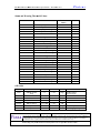
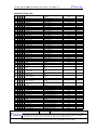
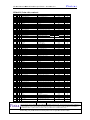
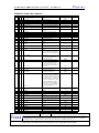
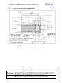
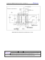
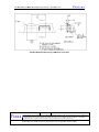
Finisar
Productt Specificaation
Multiprotoccol 80Km
m, 10Gb/ss DWDM
M XFP Op
ptical Trransceiver
FTLX
X3815M33xx
PRODU
UCT FEATU
URES
•
Gb/s to 11.35
5Gb/s
Supports 8.5G
•
Hot-pluggabl
H
le XFP footp
print
•
RoHS-6
R
Com
mpliant (lead--free)
•
100GHz ITU Grid, C-Ban
nd
•
Duplex
D
LC co
onnector
•
Power dissipaation <3.5W
W
•
Built-in
B
digitaal diagnosticc functions
•
Temperature
T
range: 0°C to
t 70°C
•
Point-to-Poin
nt & OSNR optimized
o
versions
•
APPL
LICATIONS
S
•
IT
TU G.698.1, D
DW100S-2Dxx compliant
DW
WDM 10G SO
ONET/SDH
•
IT
TU G.698.2, D
DW100C-2Axx compliant
DW
WDM 10G SO
ONET/SDH
•
DW
WDM, IEEE 10GBASE-Z
ZR based Etheernet
•
100GFC (SM-12200-LL-L) & 8GFC (SM-8800LC
C-L) compliannt
•
IT
TU G.709 / OT
TN FEC applications
Reference
R
Clo
ock Not Req
quired
S
Form Factor 10Gbb/s (XFP) trransceiver ccomplies witth
Finisar’s FTLX3815M3xx Small
X Multi-S
Source Agreeement (MSA
A) Specificaation1. It suppports ampliified DWDM
M
the XFP
10Gb
b/s SONET/SDH, 10 Gigabit Etherrnet, and 100 Gigabit Fibbre Channell applicationns
over 80km of fib
ber without dispersion compensatioon. Digital ddiagnostics functions arre
availaable via a 2-wire serial interface, ass specified iin the XFP M
MSA. The transceiver is
3
RoHS
S compliant and lead freee per Direcctive 2002/995/EC , and Finisar Appplication Notte
AN-2
20384.
PRO
ODUCT SEL
LECTION
FTLX
X3815M3xxx
xx: 100GH
Hz ITU-T chaannel
1174161
Rev.: A02
2
Page 1 of 24
This doccument contains prroprietary and confidential informatiion to Finisar Corpp. This document and the entire infoormation
contained herein, and any other tangible reprresentation thereoff, is not to be copiied, reproduced, duuplicated, distributted, or
modified
d, in whole or in paart, and/or used wiithout the expresseed written consentt of Finisar Corp.
Printed copy
c
may not be
b the latest rev
vision please rrefer to Agile fo
for current revission
FTLX
X3815M3xx DW
WDM XFP Pro
oduct Specificaation – Decembber 2013
I..
III.
Finisar
Pin Descriptions
D
Pin
1
2
3
Logic
LVTTL-I
4
LVTTL-O
5
6
7
8
9
10
11
LVTTL-I
Symbol
GND
VEE5
Mod-Desel
Interrupt
TX_DIS
VCC5
GND
VCC3
VCC3
SCL
SDA
12
LVTTL-I
LVTTLI/O
LVTTL-O
Mod_Abss
13
LVTTL-O
Mod_NR
14
15
16
17
18
19
20
21
LVTTL-O
LVTTL-I
RX_LOS
GND
GND
RDRD+
GND
VCC2
P_Down/RS
ST
22
23
24
PECL-I
VCC2
GND
RefCLK+
+
25
PECL-I
RefCLK-
CML-O
CML-O
Nam
me/Descriptioon
Module Ground
G
Optional –5.2
– Power Suupply – Not used
Module De-select;
D
Wheen held low alloows the modulle to
respond to
o 2-wire serial interface com
mmands
Interrupt (bar); Indicate s presence of aan important coondition
which can
n be read over the serial 2-wiire interface
Transmittter Disable; Traansmitter laserr source turnedd off
+5 Powerr Supply
Module Ground
G
+3.3V Po
ower Supply
+3.3V Po
ower Supply
Serial 2-w
wire interface cclock
Serial 2-w
wire interface ddata line
Reff.
1
Module Absent;
A
Indicattes module is nnot present. Groounded
in the module.
Module Not
N Ready; Finnisar defines it as a logical OR
R
between RX_LOS
R
and L
Loss of Lock inn TX/RX.
Receiver Loss of Signall indicator
Module Ground
G
Module Ground
G
Receiver inverted data ooutput
Receiver non-inverted ddata output
Module Ground
G
+1.8V Po
ower Supply – N
Not used
Power Do
own; When higgh, places the m
module in the llow
power staand-by mode annd on the fallinng edge of P_D
Down
initiates a module reset
Reset; Th
he falling edge initiates a com
mplete reset of tthe
module in
ncluding the 2--wire serial inteerface, equivallent to a
power cyccle.
+1.8V Po
ower Supply – N
Not used
Module Ground
G
Referencee Clock non-innverted input, A
AC coupled onn the
host board
d – Not Requiired
Referencee Clock inverteed input, AC cooupled on the hhost
board – Not
N Required
Module Ground
G
Module Ground
G
Transmittter inverted datta input
Transmittter non-inverteed data input
Module Ground
G
2
2
1
2
2
2
2
1
1
1
1
26
GND
1
27
GND
1
28
CML-I
TD29
CML-I
TD+
30
GND
1
Notes:
1. Module
M
circuit ground
g
is isolatted from modu
ule chassis grouund within the module.
2. Open
O
collector; should be pulled up with 4.7k – 10kohms oon host board tto a voltage bettween 3.15V
an
nd 3.6V.
1174161
Rev.: A02
2
Page 2 of 24
This doccument contains prroprietary and confidential informatiion to Finisar Corpp. This document and the entire infoormation
contained herein, and any other tangible reprresentation thereoff, is not to be copiied, reproduced, duuplicated, distributted, or
modified
d, in whole or in paart, and/or used wiithout the expresseed written consentt of Finisar Corp.
Printed copy
c
may not be
b the latest rev
vision please rrefer to Agile fo
for current revission
Finisar
FTLX
X3815M3xx DW
WDM XFP Pro
oduct Specificaation – Decembber 2013
Diagram of Hosst Board Conn
nector Block P
Pin Numbers and Names
II.
Absolute Maximum Ratings
Parameeter
Maxim
mum Supply Voltage
V
#1
Maxim
mum Supply Voltage
V
#2
Storag
ge Temperaturee
Case Operating
O
Tem
mperature
Receiv
ver Damage Th
hreshold
1174161
Symbol
Vcc3
Vcc2
TS
TOP
PRdmg
Min
-0.5
-0.5
-40
0
+5
Typ
Max
4.0
6.0
85
70
Unit
V
V
°C
°C
dBm
Rev.: A02
2
Reff.
Page 3 of 24
This doccument contains prroprietary and confidential informatiion to Finisar Corpp. This document and the entire infoormation
contained herein, and any other tangible reprresentation thereoff, is not to be copiied, reproduced, duuplicated, distributted, or
modified
d, in whole or in paart, and/or used wiithout the expresseed written consentt of Finisar Corp.
Printed copy
c
may not be
b the latest rev
vision please rrefer to Agile fo
for current revission
Finisar
FTLX
X3815M3xx DW
WDM XFP Pro
oduct Specificaation – Decembber 2013
III.
Electrica
al Characterristics (TOP = -5 to 70 °C, V CC5 = 4.75 to 5.25 Volts)
Parameeter
Supply
y Voltage #1
Supply
y Voltage #2
Supply
y Current – Vccc5 supply
Supply
y Current – Vccc3 supply
Modulle total power dissipation
Transsmitter
Input differential
d
imp
pedance
Differrential data inpu
ut swing
Transm
mit Disable Vo
oltage
Transm
mit Enable Volltage
Receiv
ver
Differrential data outp
put swing
Data output
o
rise timee
Data output
o
fall timee
LOS Fault
F
LOS Normal
N
Powerr Supply Rejection
Reference Clock (A
AC-Coupled)
Singlee-ended peak to
o peak voltage
swing
Singlee-ended resistaance
Frequeency clock toleerance
Duty cycle
c
FTL
LX3815M3xx
Symbol
Min
Vcc3
3.13
Vcc5
4.75
Icc5
Icc3
P
Rin
Vin,pp
VD
VEN
Vout,pp
tr
tf
VLOS faultt
VLOS norm
m
PSR
Typ
Max
3.46
5.25
450
750
3.5
Unit
V
V
mA
mA
W
820
Vcc
GND+ 0.8
Ω
mV
V
V
100
120
2.0
GND
500
Vcc – 0.5
GND
VSEPP
200
RL
Δf
-
40
-100
40
850
35
35
VccHOST
GND+0.5
See Note 7 below
50
mV
ps
ps
V
V
450
mV
60
+100
60
ppm
%
Reff.
1
2
3
4
5
5
6
6
7
Notes:
1. Maximum
M
total power value iss specified acro
oss the full tem
mperature and vvoltage range.
2. After
A
internal AC
A coupling.
3. Or
O open circuit.
4. In
nto 100 ohms differential
d
term
mination.
5. 20
0 – 80 %
6. Loss Of Signal is
i open collecto
or to be pulled
d up with a 4.7kk – 10kohm ressistor to 3.15 – 3.6V. Logic 0
in
ndicates normal operation; log
gic 1 indicates no signal deteected.
7. Peer Section 2.7.1. in the XFP MSA
M
Specificaation1.
1174161
Rev.: A02
2
Page 4 of 24
This doccument contains prroprietary and confidential informatiion to Finisar Corpp. This document and the entire infoormation
contained herein, and any other tangible reprresentation thereoff, is not to be copiied, reproduced, duuplicated, distributted, or
modified
d, in whole or in paart, and/or used wiithout the expresseed written consentt of Finisar Corp.
Printed copy
c
may not be
b the latest rev
vision please rrefer to Agile fo
for current revission
Finisar
FTLX
X3815M3xx DW
WDM XFP Pro
oduct Specificaation – Decembber 2013
IV.
Optical Characterist
C
tics (EOL, TOP
C, VCC5 = 4.75 to 5.25 Volts))
O = -5 to 70°C
Transmitter
Parameeter
Outpu
ut Opt. Pwr: 9/125 SMF
Opticaal Extinction Ratio
R
Center Wavelength Spacing
Transm
mitter Center Wavelength
W
–
End Of
O Life
Transm
mitter Center Wavelength
W
–
Begin
nning Of Life
Sidem
mode Suppressiion ratio
Tx Jittter Generation (peak-to-peak
k)
Tx Jittter Generation (RMS)
Symbol
POUT
ER
Min
-1
8.2
Typ
λc
X-100
100
X
λc
X-25
X
SSRmin
Txj
35
TxjRMS
Tx Lo
ocked Eye (Colld Start)
Receiv
ver
Overload
Opticall Center Wavellength
Receiv
ver Reflectancee
LOS De-Assert
D
LOS Assert
A
LOS Hysteresis
H
PMAX
λC
Rrx
LOSD
LOSA
-6
1270
M
Max
+3
Ref
X
X+100
Unit
dB
Bm
ddB
GH
Hz
ppm
X
X+25
ppm
2
0.1
ddB
U
UI
3
00.01
U
UI
4
30
s
1615
-27
-30
-37
0.5
1
2
ddBm
nnm
ddB
ddBm
ddBm
ddB
FTL
LX3815M3xx
Receiv
ver Sensitivity
y5
5
Data rate
r
(Gb//s)
BER
Dispersion
n (ps/nm)
8.5
5
9.95
10.3
10.7
11.1
11.3
1e-12
1e-12
1e-12
1e-4
1e-4
1e-4
-500 to
o 1450
-500 to
o 1450
1174161
-500 to
o 1450
-500 to
o 1450
-500 to
o 1450
-500 to
o 1450
Sensitivity
S
backk-toback at
OSNR>30dB
B
(dBm)
-24
-24
-24
-27
-27
-27
Pow
wer Penalty
at O
OSNR>30dB
(dB)
Threshold
Adjust
Required
3
3
3
3
3
3
No
No
No
Yes
Yes
Yes
Rev.: A02
2
Page 5 of 24
This doccument contains prroprietary and confidential informatiion to Finisar Corpp. This document and the entire infoormation
contained herein, and any other tangible reprresentation thereoff, is not to be copiied, reproduced, duuplicated, distributted, or
modified
d, in whole or in paart, and/or used wiithout the expresseed written consentt of Finisar Corp.
Printed copy
c
may not be
b the latest rev
vision please rrefer to Agile fo
for current revission
FTLX
X3815M3xx DW
WDM XFP Pro
oduct Specificaation – Decembber 2013
Finisar
R
OSNR
Perforrmance6
Data rate
(Gb//s)
BER
Dispersio
on (ps/nm)
Max OSN
NR w/ dispersioon at Power:
-77 to -18dBm ((dB)
8.5
5
9.95
10.3
10.7
11.1
11.3
1e-12
1e-12
1e-12
1e-4
1e-4
1e-4
-500 to
o 1450
-500 to
o 1450
-500 to
o 1450
-500 to
o 1300
-500 to
o 1300
-500 to
o 1100
28
28
28
22
22
22
6
Threshhold
Adjusttm.
Requirred
No
No
No
Yess
Yess
Yess
Notes:
1. Corresponds to approximately
y 0.8 nm.
2. X = Specified IT
TU Grid wavellength. Waveleength stability iis achieved witthin 10 secondds of power up..
3. Measured
M
with a host jitter of 50 mUI peak-tto-peak.
4. Measured
M
with a host jitter of 7 mUI RMS.
5. Measured
M
at 152
28-1600nm witth worst ER; PRBS31.
P
6. All
A OSNR meassurements are performed
p
with
h 0.1nm resoluution.
1174161
Rev.: A02
2
Page 6 of 24
This doccument contains prroprietary and confidential informatiion to Finisar Corpp. This document and the entire infoormation
contained herein, and any other tangible reprresentation thereoff, is not to be copiied, reproduced, duuplicated, distributted, or
modified
d, in whole or in paart, and/or used wiithout the expresseed written consentt of Finisar Corp.
Printed copy
c
may not be
b the latest rev
vision please rrefer to Agile fo
for current revission
FTLX
X3815M3xx DW
WDM XFP Pro
oduct Specificaation – Decembber 2013
Finisar
Part Numbers fo
or Amplified (OSNR) Application
A
s:
Channel #
17
18
19
20
21
22
23
24
25
26
27
28
29
30
31
32
33
34
35
36
37
38
39
40
41
42
43
44
45
46
47
48
49
50
51
52
53
54
55
56
57
58
59
60
61
1174161
Producct Code
FTLX38
815M317
FTLX38
815M318
FTLX38
815M319
FTLX38
815M320
FTLX38
815M321
FTLX38
815M322
FTLX38
815M323
FTLX38
815M324
FTLX38
815M325
FTLX38
815M326
FTLX38
815M327
FTLX38
815M328
FTLX38
815M329
FTLX38
815M330
FTLX38
815M331
FTLX38
815M332
FTLX38
815M333
FTLX38
815M334
FTLX38
815M335
FTLX38
815M336
FTLX38
815M337
FTLX38
815M338
FTLX38
815M339
FTLX38
815M340
FTLX38
815M341
FTLX38
815M342
FTLX38
815M343
FTLX38
815M344
FTLX38
815M345
FTLX38
815M346
FTLX38
815M347
FTLX38
815M348
FTLX38
815M349
FTLX38
815M350
FTLX38
815M351
FTLX38
815M352
FTLX38
815M353
FTLX38
815M354
FTLX38
815M355
FTLX38
815M356
FTLX38
815M357
FTLX38
815M358
FTLX38
815M359
FTLX38
815M360
FTLX38
815M361
Frequency
F
(THz
Hz)
191.7
191.8
191.9
192.0
192.1
192.2
192.3
192.4
192.5
192.6
192.7
192.8
192.9
193.0
193.1
193.2
193.3
193.4
193.5
193.6
193.7
193.8
193.9
194.0
194.1
194.2
194.3
194.4
194.5
194.6
194.7
194.8
194.9
195.0
195.1
195.2
195.3
195.4
195.5
195.6
195.7
195.8
195.9
196.0
196.1
Centerr Wavelength (n
nm)
1563.86
1563.05
1562.23
1561.42
1560.61
1559.79
1558.98
1558.17
1557.36
1556.55
1555.75
1554.94
1554.13
1553.33
1552.52
1551.72
1550.92
1550.12
1549.32
1548.51
1547.72
1546.92
1546.12
1545.32
1544.53
1543.73
1542.94
1542.14
1541.35
1540.56
1539.77
1538.98
1538.19
1537.40
1536.61
1535.82
1535.04
1534.25
1533.47
1532.68
1531.90
1531.12
1530.33
1529.55
1528.77
Rev.: A02
2
Page 7 of 24
This doccument contains prroprietary and confidential informatiion to Finisar Corpp. This document and the entire infoormation
contained herein, and any other tangible reprresentation thereoff, is not to be copiied, reproduced, duuplicated, distributted, or
modified
d, in whole or in paart, and/or used wiithout the expresseed written consentt of Finisar Corp.
Printed copy
c
may not be
b the latest rev
vision please rrefer to Agile fo
for current revission
Finisar
FTLX
X3815M3xx DW
WDM XFP Pro
oduct Specificaation – Decembber 2013
V.
Additional Specifica
ations and Response
R
Tim
ming
Parameeter
Bit Raate
Maxim
mum Supported
d Link Length
Symbol
BR
LMAX
Min
8.5
Typ
Max
11.35
80
Units
Gb/s
km
Reff.
1
2
Notes:
1. Amplified
A
SONET OC-192, 10G Ethernet, SONET
S
OC-1992 with FEC, 10G Ethernet w
with FEC,
10
0GFC, and 8GFC
2. Distance
D
indicattes dispersion budget.
b
Optical amplificationn may be requirred to achieve maximum
diistance.
Response timing::
Parameter
Tx_Diis
Min
Assert
De-asserrt
Asset
De-asserrt
Asset
De-asserrt
Asset
De-asserrt
Rx_LO
OS
Mod_N
NR
Interru
upt
P_Dow
wn/RST Time
P_Dow
wn/RST Asser Delay
Start-u
up time (Initiallize time)
1..
1174161
Typ
Max
10
2
100
100
1
1
200
500
10
100
300
Units
us
ms
us
us
ms
ms
ms
us
us
us
ms
Reff.
1
Time requirred for transponder to be read
dy to begin I2C
C communicatiion with host fr
from a cold starrt
or a hardwaare reset condittion.
Rev.: A02
2
Page 8 of 24
This doccument contains prroprietary and confidential informatiion to Finisar Corpp. This document and the entire infoormation
contained herein, and any other tangible reprresentation thereoff, is not to be copiied, reproduced, duuplicated, distributted, or
modified
d, in whole or in paart, and/or used wiithout the expresseed written consentt of Finisar Corp.
Printed copy
c
may not be
b the latest rev
vision please rrefer to Agile fo
for current revission
Finisar
FTLX
X3815M3xx DW
WDM XFP Pro
oduct Specificaation – Decembber 2013
VI.
Environm
mental Speccifications
Finisar XFP transsceivers have an operatin
ng temperatuure range froom 0°C to +70°C case
temperature.
Parameter
Case Operating
O
Tem
mperature
Storag
ge Temperaturee
VII.
Symbol
Top
Tsto
Min
0
-40
Typ
Max
70
85
Units
°C
°C
Reff.
Regulatory Complia
ance
Finisar XFP transsceivers are Class 1 Laseer Products. They are ceertified per thhe followingg
dards:
stand
Fea
ature
Agency
Standaard
Laseer Eye
Saafety
Laseer Eye
Saafety
DA/CDRH
FD
CDRH 21 CFR 1040 annd Laser Noticce 50
TÜV
TBD
Elecctrical
Saafety
Elecctrical
Saafety
TÜV
EN 6082
25-1: 1994+A111:1996+A2:20001
IEC 608
825-1: 1993+A
A1:1997+A2:20001
IEC
C 60825-2: 20000, Edition 2
EN 609950
CLASS 38862.07
CLASS 38862.87
TBD
UL/CSA
Certificate
Number
TBD
TBD
Copiees of the refeerenced certificates are available
a
at F
Finisar Corpporation upon request.
1174161
Rev.: A02
2
Page 9 of 24
This doccument contains prroprietary and confidential informatiion to Finisar Corpp. This document and the entire infoormation
contained herein, and any other tangible reprresentation thereoff, is not to be copiied, reproduced, duuplicated, distributted, or
modified
d, in whole or in paart, and/or used wiithout the expresseed written consentt of Finisar Corp.
Printed copy
c
may not be
b the latest rev
vision please rrefer to Agile fo
for current revission
FTLX
X3815M3xx DW
WDM XFP Pro
oduct Specificaation – Decembber 2013
Finisar
VIII.. Digital Diagnostics
D
Functions
F
As defined
d
by the
t XFP MSA
M 1, Finisaar XFP trannsceivers prrovide digittal diagnostiic
functtions via a 2-wire
2
serial interface, which allow
ws real-timee access to tthe followinng
operaating parameeters:
•
•
•
•
•
•
Transceiv
ver temperatu
ure
Laser biass current
Transmittted optical power
Received optical pow
wer
Transceiv
ver supply vo
oltage
TEC Tem
mperature
It also provides a sophisticateed system off alarm and warning flaggs, which m
may be used tto
w
particular operating
g parameterrs are outside of a factorry-set normaal
alert end-users when
rangee.
The operating and
a
diagnostics informaation is moonitored andd reported by a Digitaal
Diagn
nostics Tran
nsceiver Con
ntroller (DD
DTC) insidee the transceeiver, whichh is accesseed
throu
ugh the 2-wirre serial inteerface. When
n the serial pprotocol is aactivated, thhe serial clocck
signaal (SCL pin)) is generateed by the ho
ost. The possitive edge cclocks data into the XF
FP
transcceiver into those
t
segmeents of its memory
m
mapp that are nnot write-prootected. Thhe
negattive edge clo
ocks data fro
om the XFP transceiver.. The serial data signal (SDA pin) is
bi-dirrectional forr serial dataa transfer. The
T host usees SDA in cconjunction with SCL tto
mark
k the start an
nd end of seerial protoco
ol activationn. The mem
mories are orrganized as a
seriess of 8-bit daata words thaat can be ad
ddressed indiividually or sequentiallyy. The 2-wirre
seriall interface provides
p
sequ
uential or raandom accesss to the 8 bbit parameteers, addresseed
from 000h to the maximum address
a
of th
he memory.
m
detaileed informatio
on, includin
ng memory m
map definitiions, please see the XF
FP
For more
MSA
A documentation1.
Receiver Thresh
hold Adjustm
ment
The FTLX3815M
F
M3xx also prrovide access to receiverr decision thhreshold adjuustment via 22wire serial interfface, in order to improvee receiver O
OSNR perforrmance baseed on specifi
fic
link conditions.
c
It is implemeented as follo
ows:
•
1174161
Rx Threshold of XFP
P transceivers will be faactory-set foor optimizedd performancce
EC applicatiions. This will
w be the ddefault valuue during booth cold staart
in non-FE
(power-up
p) and warm
m start (modu
ule reset).
Rev.: A02
2
Page 100 of 24
This doccument contains prroprietary and confidential informatiion to Finisar Corpp. This document and the entire infoormation
contained herein, and any other tangible reprresentation thereoff, is not to be copiied, reproduced, duuplicated, distributted, or
modified
d, in whole or in paart, and/or used wiithout the expresseed written consentt of Finisar Corp.
Printed copy
c
may not be
b the latest rev
vision please rrefer to Agile fo
for current revission
FTLX
X3815M3xx DW
WDM XFP Pro
oduct Specificaation – Decembber 2013
•
•
•
Finisar
The transsceiver supports adjustm
ment of Rx T
Threshold vvalue by the host througgh
register 76d, table 01h
h. This is inttended to be used in FEC
C applicationns.
0 is a vo
olatile mem
mory. Thereffore if the ttransceiver is
Register 76d, table 01h
gister starts up
u with a vaalue of 00h w
which corresponds to thhe
power-cycled, the reg
x Threshold value.
default Rx
The thresshold adjusttment input value is 2’’s complemeent 7 bit vaalue (-128 tto
+127). The
T default Rx thresholld value willl be approxximately 0. F
Full range oof
adjustmen
nt provides at least a ±10%
±
changge in Rx thrreshold from
m the defauult
value.
SBS suppression
n, dither ton
ne
Set Address
A
111, bit 1 to “0” to enable to
one, “1” to diisable ditherr tone (defauults:
frequ
uency = 40kH
Hz , tone is disabled).
d
Please contacct your Finisar RSM or P
PLM if
BS suppresssion.
speciific amplitud
des and frequ
uencies are needed
n
for SB
Channel CDR
R Bypass ra
ate select:
8.5Gb/s Fibre-C
For 8G
8 FC operaation, write “1”
“ to Byte 116,
1 bit 1. E
Every time thhat the moduule is power
cycleed, this will need
n
to be ree-written (bitt goes back tto “0” and C
CDR is now set for
10Gb
b/s operation
n) in order to
o operate pro
operly at 8G FC.
Contaact your Finisar RSM orr PLM for deetails on the CDR Bypasss.
1174161
Rev.: A02
2
Page 11 of 24
This doccument contains prroprietary and confidential informatiion to Finisar Corpp. This document and the entire infoormation
contained herein, and any other tangible reprresentation thereoff, is not to be copiied, reproduced, duuplicated, distributted, or
modified
d, in whole or in paart, and/or used wiithout the expresseed written consentt of Finisar Corp.
Printed copy
c
may not be
b the latest rev
vision please rrefer to Agile fo
for current revission
Finisar
FTLX
X3815M3xx DW
WDM XFP Pro
oduct Specificaation – Decembber 2013
Alarm
m and Warrning Thresh
hold Valuess
Addreess
Parameeter
02-03
3
04-05
5
06-07
7
08-09
9
10-17
7
18-19
9
20-21
1
22-23
3
24-25
5
26-27
7
28-29
9
30-31
1
32-33
3
34-35
5
36-37
7
38-39
9
40-41
1
42-43
3
44-45
5
46-47
7
48-49
9
50-51
1
52-53
3
54-55
5
56-57
7
Temp High Alarm
Temp Low Alarm
Temp High Warning
W
Temp Low Warning
W
Reserved
Bias High Alarm
A
Bias Low Alarm
A
Bias High Warning
W
Bias Low Warning
W
TX Power Hig
gh Alarm
TX Power Lo
ow Alarm
TX
T Power High
h Warning
TX
T Power Low
w Warning
RX Power Hig
gh Alarm
RX Power Lo
ow Alarm
RX
R Power High
h Warning
RX
R Power Low
w Warning
AUX 1 High
h Alarm
AUX 1 Low
w Alarm
AUX 1 High Warning
AUX 1 Low Warning
W
AUX 2 High
h Alarm
AUX 2 Low
w Alarm
AUX 2 High Warning
AUX 2 Low Warning
W
Threshoold
Values
78
-13
73
-8
UNITS
120
10
110
15
+5
-3
+4
-2
-4
-31
-5
-25
57
20
54
25
3.5644
3.0366
3.465
3.135
m
mA
m
mA
m
mA
m
mA
dB
Bm
dB
Bm
dB
Bm
dB
Bm
dB
Bm
dB
Bm
dB
Bm
dB
Bm
C
C
C
C
V
V
V
V
C
C
C
C
A/D Table
T
Add
dress
96-97
98-99
100-101
102-103
104-105
106-107
108-109
1174161
Parameter
P
Intternal module
Temp
Reserved
TX
X bias current
Transmit Power
Reeceive Power
Aux
xiliary monitor1
1
Aux
xiliary monitor2
2
Accuracy
y
+/-3
Resolutioon
+/- 0.1
Units
degC
+/-8
+/-1.5 dB
B
+/-1.5 dB
B
+/-3
+/-3
+/-2
0.1
+/-0.1
+/-0.1
+/-100
uA
uW
uW
degC
uV
N
Note s
PCB mounted
thermocoupple
Laser Tempperature
3.3V Supplyy Voltage
Rev.: A02
2
Page 122 of 24
This doccument contains prroprietary and confidential informatiion to Finisar Corpp. This document and the entire infoormation
contained herein, and any other tangible reprresentation thereoff, is not to be copiied, reproduced, duuplicated, distributted, or
modified
d, in whole or in paart, and/or used wiithout the expresseed written consentt of Finisar Corp.
Printed copy
c
may not be
b the latest rev
vision please rrefer to Agile fo
for current revission
FTLX
X3815M3xx DW
WDM XFP Pro
oduct Specificaation – Decembber 2013
1174161
Finisar
Rev.: A02
2
Page 133 of 24
This doccument contains prroprietary and confidential informatiion to Finisar Corpp. This document and the entire infoormation
contained herein, and any other tangible reprresentation thereoff, is not to be copiied, reproduced, duuplicated, distributted, or
modified
d, in whole or in paart, and/or used wiithout the expresseed written consentt of Finisar Corp.
Printed copy
c
may not be
b the latest rev
vision please rrefer to Agile fo
for current revission
Finisar
FTLX
X3815M3xx DW
WDM XFP Pro
oduct Specificaation – Decembber 2013
EEPR
ROM (Tablle A0h)
Byte Addr
0
1
2
4
6
8
10
12
14
16
18
20
22
24
26
28
30
32
34
36
38
40
42
44
46
48
50
52
54
56
58
60
Bit He
ex LSB Size Name
00
0 0
8 Identifieer
01 0
8 Signal Co
onditioner Control
02
2 0 16 Temp Hiigh Alarm
04
4 0 16 Temp Lo
ow Alarm
06
6 0 16 Temp Hiigh Warning
08
8 0 16 Temp Lo
ow Warning
0A
A 0 16 Aux3 Higgh Alarm
0C
C 0 16 Aux3 Low
w Alarm
0E 0 16 Aux3 Higgh Warning
0 0 16 Aux3 Low
w Warning
10
12
2 0 16 Bias High
h Alarm
14
4 0 16 Bias Low
w Alarm
16
6 0 16 Bias High
h Warning
18
8 0 16 Bias Low
w Warning
1A
A 0 16 TX Poweer High Alarm
1C
C 0 16 TX Poweer Low Alarm
1E 0 16 TX Poweer High Warning
20
0 0 16 TX Poweer Low Warning
22
2 0 16 RX Poweer High Alarm
24
4 0 16 RX Poweer Low Alarm
26
6 0 16 RX Poweer High Warning
28
8 0 16 RX Poweer Low Warning
2A
A 0 16 AUX 1 Hiigh Alarm
2C
C 0 16 AUX 1 Lo
ow Alarm
2E 0 16 AUX 1 Hiigh Warning
30
0 0 16 AUX 1 Lo
ow Warning
32
2 0 16 AUX 2 Hiigh Alarm
34
4 0 16 AUX 2 Lo
ow Alarm
36
6 0 16 AUX 2 Hiigh Warning
38
8 0 16 AUX 2 Lo
ow Warning
3A
A 0 16 Optional VPS Control Registerrs
3C
C 0 80 RESERVEED
70
46
6
0
8
Acceptable BER
71
47
7
0
8
Actual B
BER
72
48
8
0
8
Wavelen
ngth Set MSB
73
49
9
0
8
Wavelen
ngth Set LSB
74
75
4A
A
4B
0
0
8
8
Wavelen
ngth Error MSB
Wavelen
ngth Error MSB
76
C
4C
0
8
Amplitude Adjustment
77
78
80
80
80
80
80
80
80
80
81
81
81
81
81
81
81
81
4D
D
4E
50
0
50
0
50
0
50
0
50
0
50
0
50
0
50
0
51
51
51
51
51
51
51
51
0
0
0
1
2
3
4
5
6
7
0
1
2
3
4
5
6
7
8
16
1
1
1
1
1
1
1
1
1
1
1
1
1
1
1
1
Phase Adjustment
RESERVEED
L‐ TX Pow
wer Low Alarm
L‐ TX Pow
wer High Alarm
L‐ TX Biaas Low Alarm
L‐ TX Biaas High Alarm
L‐ Vcc Lo
ow Alarm
L‐ Vcc Hiigh Alarm
L‐ Temp Low Alarm
L‐ Temp High Alarm
RESERVEED
RESERVEED
L‐ AUX 2
2 Low Alarm
L‐ AUX 2
2 High Alarm
L‐ AUX 1
1 Low Alarm
L‐ AUX 1
1 High Alarm
L‐ RX Power Low Alarm
L‐ RX Power High Alarm
1174161
Desccription
Typee of serial transceiver
Signaal Conditioner Control
MSB at low address
MSB at low address
MSB at low address
MSB at low address
MSB at low address
MSB at low address
MSB at low address
MSB at low address
MSB at low address
MSB at low address
MSB at low address
MSB at low address
MSB at low address
MSB at low address
MSB at low address
MSB at low address
MSB at low address
MSB at low address
MSB at low address
MSB at low address
MSB at low address
MSB at low address
MSB at low address
MSB at low address
MSB at low address
MSB at low address
MSB at low address
MSB at low address
Optio
onal VPS Control Regi sters
RESEERVED
Acce ptable BER Reported by the FEC to the Module
Actual BER Reported by the FEC to the Module
User input of Wavelength setpoint. (Units of nm)
0.05n
User input of Wavelength setpoint. (Units of nm)
0.05n
Monitor of Current Waveleength Error. (Units of 0.0
005nm)
Signeed 2's complement value
Relattive amplitude of receeive quantization thresshold
Phasse of receive quantizattion relative to 0.5 UI
RESEERVED
Latch
hed low TX Power alarrm.
Latch
hed high TX Power alarm.
Latch
hed low TX Bias alarm..
Latch
hed high TX Bias alarm
m.
Latch
hed low Vcc alarm.
Latch
hed high Vcc alarm.
Latch
hed low Temperature alarm.
Latch
hed high Temperaturee alarm
RESEERVED
RESEERVED
Latch
hed low AUX2 monitorr alarm.
Latch
hed high AUX2 monito
or alarm.
Latch
hed low AUX1 monitorr alarm.
Latch
hed high AUX1 monito
or alarm.
Latch
hed low RX Power alarrm.
Latch
hed high RX Power alaarm.
Value
6
0
78
‐13
73
‐8
0
0
0
0
120
10
110
15
+5
‐3
+4
‐2
‐4
‐31
‐5
‐25
57
20
54
25
3.564
3.036
3.465
3.135
0
NA
Hex Value
6
0
0
0
0
0
0
0
0
0
0
0
0
0
0
0
0
NA
FALSE
FALSE
FALSE
FALSE
FALSE
FALSE
FALSE
FALSE
NA
NA
FALSE
FALSE
FALSE
FALSE
FALSE
FALSE
0
NA
0
0
0
0
0
0
0
0
NA
NA
0
0
0
0
0
0
Rev.: A02
2
00 00 00 00 00 00 00 00 NA
Page 144 of 24
This doccument contains prroprietary and confidential informatiion to Finisar Corpp. This document and the entire infoormation
contained herein, and any other tangible reprresentation thereoff, is not to be copiied, reproduced, duuplicated, distributted, or
modified
d, in whole or in paart, and/or used wiithout the expresseed written consentt of Finisar Corp.
Printed copy
c
may not be
b the latest rev
vision please rrefer to Agile fo
for current revission
Finisar
FTLX
X3815M3xx DW
WDM XFP Pro
oduct Specificaation – Decembber 2013
EEPR
ROM (Tablle A0h) conttinued
82
82
82
82
82
82
82
82
83
83
83
83
83
83
83
83
84
84
84
52
52
52
52
52
52
52
52
53
53
53
53
53
53
53
53
54
54
54
0
1
2
3
4
5
6
7
0
1
2
3
4
5
6
7
0
1
2
1
1
1
1
1
1
1
1
1
1
1
1
1
1
1
1
1
1
1
L‐ TX Powerr Low Warning
L‐ TX Powerr High Warning
L‐ TX Bias Lo
ow Warning
L‐ TX Bias High Warning
L‐ Vcc Low W
Warning
L‐ Vcc High W
Warning
L‐ Temp Low
w Warning
L‐ Temp Higgh Warning
RESERVED
RESERVED
w Warning
L‐ AUX 3 Low
L‐ AUX 2 Higgh Warning
L‐ AUX 1 Low
w Warning
L‐ AUX 1 Higgh Warning
L‐ RX Powerr Low Warning
L‐ RX Powerr High Warning
L‐ Reset Com
mplete
L‐ MOD_NR
L‐ RX CDR no
ot Locked
84
84
84
54
54
54
3
4
5
1
1
1
L‐ LOS
L‐ RX_NR
L‐ TX CDR no
ot Locked
84
84
85
85
85
85
86
88
88
88
88
88
88
88
88
89
89
89
89
89
89
89
89
90
90
90
90
90
90
90
90
91
91
91
91
91
91
91
91
92
92
92
54
54
55
55
55
55
56
58
58
58
58
58
58
58
58
59
59
59
59
59
59
59
59
5A
A
5A
A
5A
A
5A
A
5A
A
5A
A
5A
A
5A
A
5B
B
5B
B
5B
B
5B
B
5B
B
5B
B
5B
B
5B
B
5C
C
5C
C
5C
C
6
7
0
5
6
7
0
0
1
2
3
4
5
6
7
0
1
2
3
4
5
6
7
0
1
2
3
4
5
6
7
0
1
2
3
4
5
6
7
0
1
2
1
1
5
1
1
1
16
1
1
1
1
1
1
1
1
1
1
1
1
1
1
1
1
1
1
1
1
1
1
1
1
1
1
1
1
1
1
1
1
1
1
1
L‐ TX_Fault
L‐ TX_NR
RESERVED
L‐ Wavelenggth Unlocked
L‐ TEC Fault
L‐ APD Supp
ply Fault
RESERVED
M‐ TX Poweer Low Alarm
M‐ TX Poweer High Alarm
M‐ TX Bias LLow Alarm
M‐ TX Bias H
High Alarm
M‐ Vcc Low Alarm
M‐ Vcc High
h Alarm
M‐ Temp Lo
ow Alarm
M‐ Temp Hi gh Alarm
RESERVED
RESERVED
M‐ AUX 2 Lo
ow Alarm
M‐ AUX 2 Hiigh Alarm
M‐ AUX 1 Lo
ow Alarm
M‐ AUX 1 Hiigh Alarm
M‐ RX Poweer Low Alarm
M‐ RX Poweer High Alarm
M‐ TX Poweer Low Warning
M‐ TX Poweer High Warning
M‐ TX Bias LLow Warning
M‐ TX Bias H
High Warning
M‐ Vcc Low Warning
M‐ Vcc High
h Warning
M‐ Temp Lo
ow Warning
M‐ Temp Hi gh Warning
RESERVED
RESERVED
M‐ AUX 2 Lo
ow Warning
M‐ AUX 2 Hiigh Warning
M‐ AUX 1 Lo
ow Warning
M‐ AUX 1 Hiigh Warning
M‐ RX Poweer Low Warning
M‐ RX Poweer High Warning
M‐ Reset Co
omplete
M‐ MOD_NR
R
M‐ RX CDR n
not Locked
92
92
92
5C
C
5C
C
5C
C
3
4
5
1
1
1
M‐ LOS
M‐ RX_NR
M‐ TX CDR n
not Locked
92
92
5C
C
5C
C
6
7
1
1
M‐ TX_Faultt
M‐ TX_NR
1174161
Latched low TTX Power warning.
Latched high TX Power warning.
Latched low TTX Bias warning.
Latched high TX Bias warning.
Latched low V
Vcc warning.
Latched high Vcc warning.
Latched low TTemperature warning.
Latched high Temperature warning.
RESERVED
RESERVED
Latched low A
AUX2 monitor warning.
Latched high AUX2 monitor warning.
Latched low A
AUX1 monitor warning.
Latched high AUX1 monitor warning.
Latched low RX Power warning.
Latched high RX Power warning.
Latched Reseet Complete Flag
Latched Mirror of MOD_NR pin
Latched RX C
CDR Loss of Lock
Latched mirror of LOS pin (RX optical loss of signal)
NR Status
Latched RX_N
Latched TX CDR Loss of Lock
Latched Lase r Fault condition. Generrated by laser safety ssystem.
Latched TX_N
NR Status.
RESERVED
Latched Wavvelength Unlocked Condiition
Latched TEC FFault
Latched APD Supply Fault
RESERVED
Masking bit ffor low TX Power alarm.
Masking bit ffor high TX Power alarm.
Masking bit ffor low TX Bias alarm.
Masking bit ffor high TX Bias alarm.
Masking bit ffor low Vcc alarm.
Masking bit ffor high Vcc alarm.
Masking bit ffor low Temperature alarm.
Masking bit ffor high Temperature alaarm.
RESERVED
RESERVED
Masking bit ffor low AUX2 monitor alaarm.
Masking bit ffor high AUX2 monitor al arm.
Masking bit ffor low AUX1 monitor alaarm.
Masking bit ffor high AUX1 monitor al arm.
Masking bit ffor low RX Power alarm.
Masking bit ffor high RX Power alarm..
Masking bit ffor low TX Power warnin
ng.
Masking bit ffor high TX Power warnin
ng.
Masking bit ffor low TX Bias warning.
Masking bit ffor high TX Bias warning.
Masking bit ffor low Vcc warning.
Masking bit ffor high Vcc warning.
Masking bit ffor low Temperature warning.
Masking bit ffor high Temperature waarning.
RESERVED
RESERVED
Masking bit ffor low AUX2 monitor waarning.
Masking bit ffor high AUX2 monitor w
warning.
Masking bit ffor low AUX1 monitor waarning.
Masking bit ffor high AUX1 monitor w
warning.
Masking bit ffor low RX Power warnin
ng.
Masking bit ffor high RX Power warnin
ng.
Masking bit ffor Reset Complete Flag
Masking bit ffor Mirror of MOD‐NR pin
n
Masking bit ffor RX CDR Loss of Lock
Masking bit ffor mirror of LOS pin (RX optical loss of signal )
Masking bit ffor RX_NR Status
Masking bit ffor TX CDR Loss of Lock
Masking bit ffor Laser Fault condition. Generated byy laser safety system.
Masking bit ffor TX_NR Status
FALSE
FALSE
FALSE
FALSE
FALSE
FALSE
FALSE
FALSE
N
NA
N
NA
FALSE
FALSE
FALSE
FALSE
FALSE
FALSE
FALSE
FALSE
FALSE
0
0
0
0
0
0
0
0
NA
NA
0
0
0
0
0
0
0
0
0
FALSE
FALSE
FALSE
0
0
0
FALSE
FALSE
N
NA
FALSE
FALSE
FALSE
N
NA
FALSE
FALSE
FALSE
FALSE
FALSE
FALSE
FALSE
FALSE
N
NA
N
NA
FALSE
FALSE
FALSE
FALSE
FALSE
FALSE
FALSE
FALSE
FALSE
FALSE
FALSE
FALSE
FALSE
FALSE
N
NA
N
NA
FALSE
FALSE
FALSE
FALSE
FALSE
FALSE
FALSE
FALSE
FALSE
0
0
NA
0
0
0
NA
0
0
0
0
0
0
0
0
NA
NA
0
0
0
0
0
0
0
0
0
0
0
0
0
0
NA
NA
0
0
0
0
0
0
0
0
0
FALSE
FALSE
FALSE
0
0
0
FALSE
FALSE
0
0
Rev.: A02
2
Page 155 of 24
This doccument contains prroprietary and confidential informatiion to Finisar Corpp. This document and the entire infoormation
contained herein, and any other tangible reprresentation thereoff, is not to be copiied, reproduced, duuplicated, distributted, or
modified
d, in whole or in paart, and/or used wiithout the expresseed written consentt of Finisar Corp.
Printed copy
c
may not be
b the latest rev
vision please rrefer to Agile fo
for current revission
Finisar
FTLX
X3815M3xx DW
WDM XFP Pro
oduct Specificaation – Decembber 2013
EEPR
ROM (Tablle A0h) conttinued
93
5D
D
0
5
RESERVED
93
93
93
94
96
97
5D
D
5D
D
5D
D
5EE
60
0
61
1
5
6
7
0
0
0
1
1
1
16
8
8
M‐ Wavelength Unlocked
M‐ TEC Fault
M‐ APD Sup
pply Fault
RESERVED
Temperatu
ure MSB
Temperatu
ure LSB
98
62
2
0
8
Vcc MSB
99
100
101
102
103
104
105
63
3
64
4
65
5
66
6
67
7
68
8
69
9
0
0
0
0
0
0
0
8
8
8
8
8
8
8
Vcc LSB
TX Bias MSB
B
TX Bias LSB
B
TX Power M
MSB
TX Power LLSB
RX Power M
MSB
RX Power LLSB
106
6A
A
0
8
AUX 1 MSB
107
6B
B
0
8
AUX 1 LSB
108
6C
C
0
8
AUX 2 MSB
109
6D
D
0
8
AUX 2 LSB
110
6EE
0
1
Data_Not_R
Ready
110
110
6EE
6EE
1
2
1
1
LOS
Interrupt
110
6EE
3
1
Soft P_Dow
wn
110
6EE
4
1
P_Down State
110
6EE
5
1
MOD_NR Sttate
RESERVED
Masking bitt for Wavelength Unlockked Condition
Masking bitt for TEC Fault
Masking bitt for APD Supply Fault
RESERVED
measured module tempeerature
Internally m
Internally m
measured module tempeerature
Internally m
measured supply voltagee in transceiver
measured supply voltagee in Internally m
transceiver
measured TX Bias Curren
nt
Internally m
Internally m
measured TX Bias Curren
nt
Measured TTX output power
Measured TTX output power
Measured R
RX output power
Measured R
RX output power
Auxiliary measurement 1 defined i n Byte 222 Page 01h
Auxiliary measurement 1 defined i n Byte 222 Page 01h
Auxiliary measurement 2 defined i n Byte 222 Page 01h
Auxiliary measurement 2 defined i n Byte 222 Page 01h
Indicates transceiver has achieved power up and data is ready. Bit remains high until data be read at which time th
he device is ready to b
sets the bit low.
Indicates Optical Loss of Signal (perr relevant optical link standard). Updated within 100msec of change on pin
Digital statee of the Interrupt outputt pin
Read/write bit that allows the mod
dule to be he power down mode. TThis is placed in th
identical to the P_Down hardware pin function except that it does not inittiate a system reseet
Digital statee of the P_Down Pin. Up
pdated within 100m
msec of change on pin
Digital statee of the MOD_NR Pin. Up
pdated within 100m
msec of change on pin
110
6EE
6
1
Soft TX Disaable
110
111
111
6EE
6F
6F
7
0
3
1
3
1
TX Disable State
RESERVED
RX_CDR not Locked
111
111
6F
6F
4
5
1
1
RX_NR Statte
TX_CDR nott Locked
111
6F
6
1
TX_Fault Sttate
111
112
6F
70
0
7
0
1 TX_NR Statte
48 RESERVED
Read/write bit that allows softwaree disable of laser. Wrriting '1' disables laser. TTurn on/off time is 100m
msec max from acknowl edgement of serial bytte transmission. This bitt is "OR"d with the hard TX_DISABLE pin valuee. Note, A TX_DISABLE pin is defaault per SFP MSA
enabled unless pulled low by hardw
ware. If d, the Soft TX Disaable is not implemented
transceiver ignores the value of thi s bit. wer up value is 0.
Default pow
Digital statee of the TX Disable Inputt Pin. Updated wi thin 100msec of change on pin
RESERVED
DR
Identifies Loss of Lock in RX path CD
Not Ready condition as specific to Identifies N
the TX path
DR
Identifies Loss of Lock in TX path CD
Identifies Laser fault conditoin (Ge nerated by laser safety system)
Not Ready condition as specific to Identifies N
the TX path
RESERVED
118
118
119
123
127
76
6
76
6
77
7
7B
B
7F
0
1
0
0
0
1
7
32
32
8
Error Checking
RESERVED
Password
Location of Entry of New Optional P
word
Location forr Entry of Optional Passw
Entry Locati on for Table Select Bytee
1174161
Error Checkking
RESERVED
New Passw
word Entry
Password EEntry
Table Selecct
NA
NA
FFALSE
F
FALSE
F
FALSE
NA
0
0
0
0
0
NA
0
0
0
0
0
0
0
0
0
0
0
0
0
0
0
0
0
0
0
0
0
0
0
0
0
0
0
0
FFALSE
F
FALSE
0
0
F
FALSE
0
F
FALSE
0
F
FALSE
0
0
0
F
FALSE
0
F
FALSE
0
FFALSE
F
FALSE
0
0
F
FALSE
0
FFALSE
NA
Packet erro
or checking not sup
pported
NA
0
0
1
0
NA
0
NA
00 00 00 00 00 00 00 00 1
Rev.: A02
2
Page 166 of 24
This doccument contains prroprietary and confidential informatiion to Finisar Corpp. This document and the entire infoormation
contained herein, and any other tangible reprresentation thereoff, is not to be copiied, reproduced, duuplicated, distributted, or
modified
d, in whole or in paart, and/or used wiithout the expresseed written consentt of Finisar Corp.
Printed copy
c
may not be
b the latest rev
vision please rrefer to Agile fo
for current revission
Finisar
FTLX
X3815M3xx DW
WDM XFP Pro
oduct Specificaation – Decembber 2013
EEPR
ROM (Tablle 01h)
Byte Bit Addr Hexx LSB Size Name
128 80
0 0
8 Identifier
129 81
1 0
3 RESERVED
Description
n
Type of serrial transceiver
RESERVED
129
129
129
129
130
131
131
131
131
131
131
131
131
132
132
132
132
132
133
134
134
134
134
134
134
134
134
135
135
135
135
135
135
135
136
136
136
136
136
136
136
136
137
137
137
137
137
137
137
137
138
138
138
138
139
139
139
139
139
139
139
140
141
81
1
81
1
81
1
81
1
82
2
83
3
83
3
83
3
83
3
83
3
83
3
83
3
83
3
84
4
84
4
84
4
84
4
84
4
85
5
86
6
86
6
86
6
86
6
86
6
86
6
86
6
86
6
87
7
87
7
87
7
87
7
87
7
87
7
87
7
88
8
88
8
88
8
88
8
88
8
88
8
88
8
88
8
89
9
89
9
89
9
89
9
89
9
89
9
89
9
89
9
8A
A
8A
A
8A
A
8A
A
8B
B
8B
B
8B
B
8B
B
8B
B
8B
B
8B
B
8C
C
8D
D
3
4
5
6
0
0
1
2
3
4
5
6
7
0
4
5
6
7
0
0
1
2
3
4
5
6
7
0
2
3
4
5
6
7
0
1
2
3
4
5
6
7
0
1
2
3
4
5
6
7
0
5
6
7
0
2
3
4
5
6
7
0
0
1
1
1
2
8
1
1
1
1
1
1
1
1
4
1
1
1
1
8
1
1
1
1
1
1
1
1
2
1
1
1
1
1
1
1
1
1
1
1
1
1
1
1
1
1
1
1
1
1
1
5
1
1
1
2
1
1
1
1
1
1
8
8
CLEI code p
present in Table 02h
TX Ref Clocck Input Required
Module wi th CDR
Ext.Identifier
Connector
RESERVED
10GBASE‐EW
10GBASE‐LW
W
10GBASE‐SW
10GBASE‐LRM
10GBASE‐ER
10GBASE‐LR
10GBASE‐SR
RESERVED
Intermediaate Reach 1300 nm FP
Extented R
Reach 1550 nm
1200‐SM‐LLL‐L
1200‐MX‐SN‐I
RESERVED
RESERVED
OC‐48‐LR
OC‐48‐IR
OC‐48‐SR
2xFC SMF
2xFC MMF
1000BASE‐LLX/1xFC SMF
1000BASE‐SSX/1xFC MMF
RESERVED
I‐64.5
I‐64.3
I‐64.2
I‐64.2r
I‐64.1
I‐64.1r
RESERVED
S‐64.5b
S‐64.5a
S‐64.3b
S‐64.3a
S‐64.2c
S‐64.2a
S‐64.1
RESERVED
DWDM
G.959.1 P1LL1‐2D2
L‐64.3
L‐64.2c
L‐64.2b
L‐64.2a
L‐64.1
RESERVED
V‐64.3
V‐64.2b
V‐64.2a
RESERVED
Tx Dither Supported
RZ
NRZ
Sonet Scram
mbled
8B/10B
64B/66B
BR, minimu
um
BR, maximum
CLEI code p
present in Table 02h
TX Ref Clocck Input Required
Module witth CDR
Defines Mo
odule Power Class
Code for co
onnector type
RESERVED
10GBASE‐EW
W
10GBASE‐LW
W
10GBASE‐SW
W
10GBASE‐LR
RM
10GBASE‐ER
R
10GBASE‐LR
R
10GBASE‐SR
R
RESERVED
Intermediaate Reach 1300 nm FP
Extented Reeach 1550 nm
1200‐SM‐LLL‐L
1200‐MX‐SN
N‐I
RESERVED
RESERVED
Lower speeed link compliance code
Lower speeed link compliance code
Lower speeed link compliance code
Lower speeed link compliance code
Lower speeed link compliance code
Lower speeed link compliance code
Lower speeed link compliance code
RESERVED
Sonet code s
Sonet code s
Sonet code s
Sonet code s
Sonet code s
Sonet code s
RESERVED
Sonet Shortt Haul Link codes
Sonet Shortt Haul Link codes
Sonet Shortt Haul Link codes
Sonet Shortt Haul Link codes
Sonet Shortt Haul Link codes
Sonet Shortt Haul Link codes
Sonet Shortt Haul Link codes
RESERVED
DWDM
Sonet Long Haul Link codes
Sonet Long Haul Link codes
Sonet Long Haul Link codes
Sonet Long Haul Link codes
Sonet Long Haul Link codes
Sonet Long Haul Link codes
RESERVED
Sonet Very Long Haul Link codes
Sonet Very Long Haul Link codes
Sonet Very Long Haul Link codes
RESERVED
142
8EE
0
8
Length(SMF)‐km
143
8FF
0
8
Length(EMM‐50um)‐meter
LENGTH (STTANDARD SINGLE MODE FIBER)‐KM
LENGTH (EX
XTENDED BANDWIDTH 50 um MULTIMOD
DE FIBER) (/2m)
1174161
upport
Encoding Su
Encoding Su
upport
Encoding Su
upport
Encoding Su
upport
Encoding Su
upport
Minimum SSupported Bitrate (/100M
Mb)
MaximumSSupported Bitrate (/100M
Mb)
Value
V
XFP
NA
No CLEI code present in Taable 02h
Not Required
with CDR
Power le vel 3 ( < 3.5W )
LC
NA
FALSE
FALSE
FALSE
FALSE
FALSE
FALSE
FALSE
NA
FALSE
FALSE
FALSE
FALSE
NA
NA
FALSE
FALSE
FALSE
FALSE
FALSE
FALSE
FALSE
NA
FALSE
FALSE
FALSE
FALSE
FALSE
FALSE
NA
FALSE
FALSE
FALSE
FALSE
FALSE
FALSE
FALSE
NA
FALSE
TRUE
FALSE
FALSE
FALSE
FALSE
FALSE
NA
FALSE
FALSE
FALSE
NA
TRUE
FALSE
TRUE
TRUE
TRUE
TRUE
99
113
He
ex Value
6
NA
80
50
0
0
0
1
0
2
7
NA
0
0
0
0
0
0
0
NA
0
0
0
0
NA
NA
0
0
0
0
0
0
0
NA
0
0
0
0
0
0
NA
0
0
0
0
0
0
0
NA
0
1
0
0
0
0
0
NA
0
0
0
NA
1
0
1
1
1
1
63
71
Rev.: A02
2
Page 177 of 24
This doccument contains prroprietary and confidential informatiion to Finisar Corpp. This document and the entire infoormation
contained herein, and any other tangible reprresentation thereoff, is not to be copiied, reproduced, duuplicated, distributted, or
modified
d, in whole or in paart, and/or used wiithout the expresseed written consentt of Finisar Corp.
Printed copy
c
may not be
b the latest rev
vision please rrefer to Agile fo
for current revission
Finisar
FTLX
X3815M3xx DW
WDM XFP Pro
oduct Specificaation – Decembber 2013
EEPR
ROM (Tablle 01h) conttinued
144
90
0
8
Length(50)‐m
meter
145
146
147
147
147
147
147
91
92
93
93
93
93
93
0
0
0
1
2
3
4
8
8
1
1
1
1
4
Length(62.5))‐meter
Length(Copp
per)‐km
Tunable Tran
nsmitter
Detector Typ
pe
Cooled Transmitter
Wavelength Control
Transmitter Technology
148
164
164
164
164
164
164
164
164
165
168
94
A4
A4
A4
A4
A4
A4
A4
A4
A5
A8
0
0
1
2
3
4
5
6
7
0
0
128
1
1
1
1
1
1
1
1
24
128
184
B8
0
16 Vendor Rev
186
BA
0
16 Wavelength
188
190
191
BC
BE
BF
0
0
0
16 Wavelength Tolerance
8 Max Case Teemp
8 CC_BASE
192
C0
0
8
Maximum Po
ower
193
C1
0
8
Max Power iin Power Down Mode
194
C2
0
4
Max Currentt +3.3v
194
C2
4
4
Max Currentt +5v
195
C3
0
4
Max Currentt ‐5v
195
196
C3
C4
4
0
4 Max Currentt +1.8v
128 Vendor SN
212
D4
0
16 Date Code ‐ Year
214
216
D6
D8
0
0
16 Date Code ‐ Month
16 Date Code ‐ Day
218
220
220
220
220
221
221
221
221
221
221
221
221
222
222
223
DA
DC
DC
DC
DC
DD
DD
DD
DD
DD
DD
DD
DD
DE
DE
DF
0
0
3
4
5
0
1
2
3
4
5
6
7
0
4
0
16
3
1
1
3
1
1
1
1
1
1
1
1
4
4
8
224
E0
0
256 Vendor Speccific
1174161
Vendor Nam
me
XFI Loopback Supported
Lineside Loo
opback Mode Supported
RESERVED
CDR supportt for 11.1 Gb/s
CDR supportt for 10.7 Gb/s
CDR supportt for 10.5 Gb/s
CDR supportt for 10.3 Gb/s
CDR supportt for 9.95 Gb/s
Vendor OUI
Vendor PN
Date Code ‐ Vendor specific lot code
RESERVED
ower meas. Type
Received po
FEC BER support
AUX3 (Finisaar)
Optional CM
MU support mode
Wavelength Tunability implemented
d
Active FEC co
ontrol function umplemeented
Support VPSS bypass regulator mode
Suport VPS LLV regulator mode
Soft P_Down
n
Soft TX_DISA
ABLE
Variable Pow
wer Supply Support
Aux A/D Inp
put 2
Aux A/D Inp
put 1
CC_EXT
LENGTH (50 UM
M MULTIMODE FIBER) (/1m
meter)
LENGTH (62.5 U
UM MULTIMODE FIBER)(/1meteer)
LENGTH (COPP
PER) (/1meter)
Device Techno
ology
Device Techno
ology
Device Techno
ology
Device Techno
ology
Device Techno
ology
0
0
0
0
FALSEE
APD
TRUEE
FALSEE
1550 nm EML
0
0
0
1
1
0
7
46 69 6E 69 73 61 72 20 20 20 20 20 20 20 20 20
1
0
NA
1
1
1
1
1
00 90 65
5 Variablee
Finisaar
Vendor Name (ascii)
TRUEE
CDR support
FALSEE
CDR support
NA
RESERVED
TRUEE
CDR support
TRUEE
CDR support
TRUEE
CDR support
TRUEE
CDR support
TRUEE
CDR support
00 90 65h (36965
5 Decimal)
SFP vendor IEEEE company ID
Part number provided by vendor (ASCII)
FTLX3815M
M3xx
Revision level for part number provideed by vendor (ASCII)
0
Nominal laser wavelength Variable
(Wavelength=vvalue/20 in nm)
Guaranteed range of laser wavelength (+/‐ ominal wavelength.
value) from No
20
(Wavelength TTol. = value/200 in nm)
MAXIMUM CASSE TEMPERATURE
70
Checksum (128
8 to 190)
Maximum Pow
wer Dissipation, Max pow
wer is 8 175
bit value * 20 m
mW.
Maximum Totaal Power Dissipation in Power Down Mode, M
Max Power is 8 bit value ** 10 mW.
150
Maximum currrent required by +3.3V Su
upply. Max current is 4 bit value * 100 mA.
8
Maximum currrent required by +5V Supply.Max current is 4 bit value * 50 m
mA. [500 mA max]
9
Maximum currrent required by ‐5.2V Supply.Max current is 4 bit value * 50 m
mA. 0
[500 mA max]
upply. Maximum currrent required by +1.8V Su
Max current is 4 bit value * 100 mA.
0
Serial number provided by vendor (ASC
CII)
Variable
Two low orderr digits of year (00 = 2000)) ‐ Variable
ASCII code
Digits of month (01=JAN ~ 12=DEC) ‐ ASCII Variable
code
01‐31) ‐ ASCII code
Variable
Digits of day (0
Vendor specifiic lot code, may be left blank ‐ ASCII code
0
RESERVED
NA
ons
Special functio
Average power
Special functio
ons
FALSEE
Aux3 minitor ( 1612 only)
RESERVED
Enhanced Optiions
FALSEE
Enhanced Optiions
FALSEE
Enhanced Optiions
TRUEE
Enhanced Optiions
FALSEE
Enhanced Optiions
FALSEE
Enhanced Optiions
TRUEE
Enhanced Optiions
TRUEE
Enhanced Optiions
FALSEE
Enhanced Optiions
+3.3V Supply Voltage
Enhanced Optiions
Laser Tempeerature
Check code forr bytes 192 to 222
Vendor Specific EEPROM
0
Variablee
Variablee
00 14 46
Variablee
AF
96
8
9
0
0
Variablee
Variablee
Variablee
Variablee
0
NA
1
0
0
0
0
1
0
0
1
1
0
7
4
Variablee
00000000000
00000
00000000000
00000
00000000000
00000
00000000000
00000
0000
Rev.: A02
2
Page 18 of 24
This doccument contains prroprietary and confidential informatiion to Finisar Corpp. This document and the entire infoormation
contained herein, and any other tangible reprresentation thereoff, is not to be copiied, reproduced, duuplicated, distributted, or
modified
d, in whole or in paart, and/or used wiithout the expresseed written consentt of Finisar Corp.
Printed copy
c
may not be
b the latest rev
vision please rrefer to Agile fo
for current revission
FTLX
X3815M3xx DW
WDM XFP Pro
oduct Specificaation – Decembber 2013
Finisar
EEPR
ROM (Tablle 02h)
Filled witth “00” unlesss otherwisee specified byy customer rrequirementss.
IX.
Mechaniccal Specifications
Finisar’s XFP traansceivers arre compliant with the dim
mensions defined by the XFP Multi-Sourccing Agreem
ment (MSA).
77.95
22.15
18.35
13.30
8.50
LATCHED
1.95
16.00
U
UNLATCHED
D
2
20.85
39.00
R1..00
XF
FP Transceiveer (dimensionss are in mm)
1174161
Rev.: A02
2
Page 199 of 24
This doccument contains prroprietary and confidential informatiion to Finisar Corpp. This document and the entire infoormation
contained herein, and any other tangible reprresentation thereoff, is not to be copiied, reproduced, duuplicated, distributted, or
modified
d, in whole or in paart, and/or used wiithout the expresseed written consentt of Finisar Corp.
Printed copy
c
may not be
b the latest rev
vision please rrefer to Agile fo
for current revission
FTLX
X3815M3xx DW
WDM XFP Pro
oduct Specificaation – Decembber 2013
X.
Finisar
PCB Lay
yout and Bezzel Recomm
mendations
XFP Host Bo
oard Mechaniical Layout (d
dimensions aree in mm)
1174161
Rev.: A02
2
Page 200 of 24
This doccument contains prroprietary and confidential informatiion to Finisar Corpp. This document and the entire infoormation
contained herein, and any other tangible reprresentation thereoff, is not to be copiied, reproduced, duuplicated, distributted, or
modified
d, in whole or in paart, and/or used wiithout the expresseed written consentt of Finisar Corp.
Printed copy
c
may not be
b the latest rev
vision please rrefer to Agile fo
for current revission
FTLX
X3815M3xx DW
WDM XFP Pro
oduct Specificaation – Decembber 2013
Finisar
XF
FP Detail Host Board Mech
hanical Layoutt (dimensions are in mm)
1174161
Rev.: A02
2
Page 21 of 24
This doccument contains prroprietary and confidential informatiion to Finisar Corpp. This document and the entire infoormation
contained herein, and any other tangible reprresentation thereoff, is not to be copiied, reproduced, duuplicated, distributted, or
modified
d, in whole or in paart, and/or used wiithout the expresseed written consentt of Finisar Corp.
Printed copy
c
may not be
b the latest rev
vision please rrefer to Agile fo
for current revission
FTLX
X3815M3xx DW
WDM XFP Pro
oduct Specificaation – Decembber 2013
Finisar
XFP Recom
mmended Bezzel Design (dim
mensions are iin mm)
1174161
Rev.: A02
2
Page 222 of 24
This doccument contains prroprietary and confidential informatiion to Finisar Corpp. This document and the entire infoormation
contained herein, and any other tangible reprresentation thereoff, is not to be copiied, reproduced, duuplicated, distributted, or
modified
d, in whole or in paart, and/or used wiithout the expresseed written consentt of Finisar Corp.
Printed copy
c
may not be
b the latest rev
vision please rrefer to Agile fo
for current revission
FTLX
X3815M3xx DW
WDM XFP Pro
oduct Specificaation – Decembber 2013
Finisar
XI. Notes & Ex
xceptions
•
The FTLX
X3815 produ
uct family haas the follow
wing exceptioons to the X
XFP MSA;
o In
nitialize time of 2 sec maaximum (MS
SA requires 3300ms).
•
XFI loopb
back operation:
o When
W
XFI Loopback is en
nabled, the T
Transmitter ooutput is disaabled.
o When
W
Line Lo
oopback is en
nabled, the R
Receiver inpput is disableed.
•
o
req
quires config
guration channge via I2C vvendor reserrved
8.5Gb/s operation
command
d.
XII.
Referencces
1.
10 Gigabiit Small Forrm Factor Plu
uggable Moodule (XFP) Multi-Sourcce Agreemennt
(MSA), Rev
R
4.5 – August 20
005. Docum
mentation iss currently available aat
http://ww
ww.xfpmsa.orrg/
2.
Applicatio
on Note AN
N-2035: “Diigital Diagnnostic Monittoring Interfface for XF
FP
Optical Transceivers”” – Finisar Corporation,
C
December 22003
3.
Directive 2002/95/EC
C of the Eu
uropean Couuncil Parliam
ment and off the Counciil,
“on the restriction
r
off the use off certain hazzardous subbstances in eelectrical annd
electronicc equipment””. January 27
7, 2003.
4.
“Applicattion Note AN
N-2038: Finiisar Implemeentation Of R
RoHS Comppliant
Transceiv
vers”, Finisarr Corporatio
on, January 221, 2005.
1174161
Rev.: A02
2
Page 233 of 24
This doccument contains prroprietary and confidential informatiion to Finisar Corpp. This document and the entire infoormation
contained herein, and any other tangible reprresentation thereoff, is not to be copiied, reproduced, duuplicated, distributted, or
modified
d, in whole or in paart, and/or used wiithout the expresseed written consentt of Finisar Corp.
Printed copy
c
may not be
b the latest rev
vision please rrefer to Agile fo
for current revission
FTLX
X3815M3xx DW
WDM XFP Pro
oduct Specificaation – Decembber 2013
Finisar
XIII.. Product Selection
S
Deetails
FTLX381
15M3xx
FT: FT Seeries
L: RoHS--6
X: 10G Bit
B Rate Class
38: 80km (asymmetriic chirp)
1: XFP fo
orm factor
5: Standarrd Performan
nce Class
M: Multip
protocol
3: Commeercial tempeerature rangee
xx: Sub-B
Band start ch
hannel (pleasse refer to paage 6 for chaannel definittion)
XIV.. Revision History
vision
Rev
Date
A00
A
8/15/2012
Prelimin
nary document created
A01
A
10/22/2012
Update EEPROM
E
Tablle A0h and 01hh
A02
A
10/31/2012
Include cold
c
start timinng, correct initiialization timinng, SBS/Ditherr
Byte
XV.
Descrip
ption
For moree informatio
on
Finisar Corporatiion
1389 Moffett Parrk Drive
nyvale, CA 94089-1133
9
Sunn
000
Tel. 1-408-548-1
1
Fax 1-408-541-6
1
138
sales@
@finisar.com
m
www
w.finisar.com
m
1174161
Rev.: A02
2
Page 244 of 24
This doccument contains prroprietary and confidential informatiion to Finisar Corpp. This document and the entire infoormation
contained herein, and any other tangible reprresentation thereoff, is not to be copiied, reproduced, duuplicated, distributted, or
modified
d, in whole or in paart, and/or used wiithout the expresseed written consentt of Finisar Corp.
Printed copy
c
may not be
b the latest rev
vision please rrefer to Agile fo
for current revission