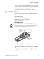
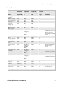
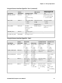
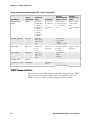
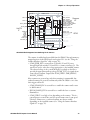
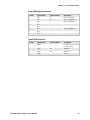
1
Service Manual
CK30 Handheld
Computer
Intermec Technologies Corporation
Corporate Headquarters
6001 36th Ave. W.
Everett, WA 98203
U.S.A.
www.intermec.com
The information contained herein is proprietary and is provided solely for the purpose of allowing customers
to operate and service Intermec-manufactured equipment and is not to be released, reproduced, or used for
any other purpose without written permission of Intermec.
Information and specifications contained in this document are subject to change without prior notice and do
not represent a commitment on the part of Intermec Technologies Corporation.
© 2004 by Intermec Technologies Corporation. All rights reserved.
The word Intermec, the Intermec logo, Norand, ArciTech, CrossBar, Data Collection Browser, dcBrowser,
Duratherm, EasyCoder, EasyLAN, Enterprise Wireless LAN, EZBuilder, Fingerprint, i-gistics, INCA (under
license), InterDriver, Intermec Printer Network Manager, IRL, JANUS, LabelShop, Mobile Framework,
MobileLAN, Nor*Ware, Pen*Key, Precision Print, PrintSet, RoutePower, TE 2000, Trakker Antares, UAP,
Universal Access Point, and Virtual Wedge are either trademarks or registered trademarks of Intermec
Technologies Corporation.
Throughout this manual, trademarked names may be used. Rather than put a trademark (™ or ®) symbol in
every occurrence of a trademarked name, we state that we are using the names only in an editorial fashion,
and to the benefit of the trademark owner, with no intention of infringement.
There are U.S. and foreign patents pending.
Wi-Fi is a registered certification mark of the Wi-Fi Alliance.
Microsoft, Windows, and the Windows logo are registered trademarks of Microsoft Corporation in the
United States and/or other countries.
Bluetooth is a trademark of Bluetooth SIG, Inc., U.S.A.
This product includes software developed by the OpenSSL Project for use in the OpenSSL Toolkit.
(http://www.opensssl.org/).
This product includes cryptographic software written by Eric Young ([email protected]).
This product uses Regex++, Index software during its operational phases. The owner of Regex++ has granted
use of the software to anyone provided such use is accompanied by the following copyright and permission
notice:
Regex++, Index. (Version 3.31, 16th Dec 2001)
Copyright © 1998-2001 Dr John Maddock
Permission to use, copy, modify, distribute and sell this software and its documentation for any purpose is
hereby granted without fee, provided that the above copyright notice appear in all copies and that both that
copyright notice and this permission notice appear in supporting documentation. Dr John Maddock makes
no representations about the suitability of this software for any purpose. It is provided "as is" without express
or implied warranty.
ii
CK30 Handheld Computer Service Manual
Contents
Contents
Before You Begin ............................................................................................................. vii
Safety Summary .................................................................................................. vii
Safety Icons........................................................................................................ viii
Global Services and Support................................................................................. ix
Who Should Read This Document?...................................................................... x
1
Troubleshooting .......................................................................................................................... 1
2
Replacing Parts ............................................................................................................................. 7
Troubleshooting the CK30 ................................................................................................ 2
Cautions ............................................................................................................................ 8
Replacing Parts................................................................................................................... 9
Opening the CK30 ............................................................................................... 9
Replacing the 802.11b/g Radio and Antenna ...................................................... 10
Replacing the Ethernet Card ............................................................................... 12
Replacing the Bluetooth Radio............................................................................ 13
Replacing the Main PCB..................................................................................... 15
Replacing the Bezel Assembly.............................................................................. 17
Replacing the Display Assembly .......................................................................... 18
Replacing the Keypad Assembly ............................................................................ 20
Replacing the SE1200 Scanner.............................................................................. 21
Replacing the EV10 Scanner ............................................................................... 23
Replacing the IT4000 Imager.............................................................................. 25
Replacing the Tethered Scanner .......................................................................... 25
Closing the CK30 ................................................................................................. 27
3
Spare Parts List and Exploded Views ............................................................................. 29
CK30 Exploded View ...................................................................................................... 30
CK30 Spare Parts List ...................................................................................................... 31
Ethernet Card Assembly Exploded View .......................................................................... 32
Ethernet Card Assembly Spare Parts List .......................................................................... 32
SE1200 Scan Engine Assembly Exploded View ................................................................ 33
SE1200 Scan Engine Assembly Spare Parts List................................................................ 33
EV10 Scan Engine Assembly Exploded View ................................................................... 34
EV10 Scan Engine Assembly Spare Parts List ................................................................... 34
CK30 Handheld Computer Service Manual
iii
Contents
IT4000 Imager Assembly Exploded View......................................................................... 35
IT4000 Imager Assembly Spare Parts List ........................................................................ 35
Tethered Scan Flex Assembly Exploded View................................................................... 36
Tethered Scan Flex Assembly Spare Parts List................................................................... 36
Safety Labels Exploded View ............................................................................................ 37
Safety Labels Spare Parts List............................................................................................ 37
4
Theory of Operation ................................................................................................................ 39
System Architecture ......................................................................................................... 40
Processor Core ................................................................................................................. 41
Processor............................................................................................................. 41
System Clocks ..................................................................................................... 41
Memory .............................................................................................................. 42
I/O Signals....................................................................................................................... 43
I2C Bus ........................................................................................................................... 47
FPGA............................................................................................................................... 47
FPGA Download ................................................................................................ 48
FPGA Power Management.................................................................................. 49
FPGA Bus Interface ............................................................................................ 50
FPGA Clocks ...................................................................................................... 50
Power System................................................................................................................... 51
Architecture, Power Supplies............................................................................... 51
Main Battery....................................................................................................... 52
Supercap ............................................................................................................. 53
External Power.................................................................................................... 53
Power Management Architecture ..................................................................................... 54
Device Power States ............................................................................................ 56
Power Supply Controller (PSC) .......................................................................... 59
Battery Status Monitoring................................................................................... 60
Low-Battery Handling ........................................................................................ 61
Battery Status LED ............................................................................................. 62
Reset Control...................................................................................................... 63
I/O Control ........................................................................................................ 64
Resume Events .................................................................................................... 65
Suspend Events ................................................................................................... 66
Display............................................................................................................................. 66
LCD Panel.......................................................................................................... 66
LCD Controller .................................................................................................. 66
Bias Supply ......................................................................................................... 66
iv
CK30 Handheld Computer Service Manual
Contents
Display Contrast Control.................................................................................... 66
Temperature Compensation................................................................................ 67
Backlight............................................................................................................. 67
Keypad............................................................................................................................. 67
Key Matrix Scanning........................................................................................... 67
Wakeup Keys ...................................................................................................... 68
I/O Key .............................................................................................................. 69
Scan Buttons....................................................................................................... 69
Keypad ID .......................................................................................................... 69
Network Interface ............................................................................................................ 69
Mini PCI Interface.............................................................................................. 69
802.11b/g Radio ................................................................................................. 74
10/100Mb Ethernet ............................................................................................ 74
Scanners........................................................................................................................... 74
Scanner Interface................................................................................................. 76
1D DBP Scanner Interface.................................................................................. 78
Wands and Wand Emulation.............................................................................. 80
2D Imagers ......................................................................................................... 80
1D MDS Scanner Interface................................................................................. 82
Serial (RSTTL) Scanner Interface........................................................................ 82
Scanner Power .................................................................................................... 83
Tethered Scanners............................................................................................... 83
Tethered Scanner Support Through Dock Connector......................................... 85
Trigger and Scanner Control............................................................................... 87
Scanning and Good Read Indication................................................................... 87
Dock Interface ................................................................................................................. 87
USB Port ............................................................................................................ 89
RS-232 Port........................................................................................................ 89
Scanner Interface................................................................................................. 90
Bluetooth ......................................................................................................................... 90
Storage Card (SD card) .................................................................................................... 91
Beeper.............................................................................................................................. 92
Debug Support ................................................................................................................ 93
Field-Access Debug Port ..................................................................................... 93
Debug Board ...................................................................................................... 94
Firmware Upgrade ........................................................................................................... 95
Bootloader .......................................................................................................... 95
OS Image............................................................................................................ 95
In-System Programmability of Programmable Devices ........................................ 96
Accessories ....................................................................................................................... 96
Connector Pin-Outs............................................................................................ 96
AD1 1-Bay Communications Dock .................................................................... 99
AD2 4-Bay Communications Dock .................................................................. 100
CK30 Handheld Computer Service Manual
v
Contents
AC1 4-Slot Battery Charger .............................................................................. 101
AC2 4-Bay Charging Dock ............................................................................... 102
vi
CK30 Handheld Computer Service Manual
Before You Begin
Before You Begin
This section provides you with safety information, technical support
information, and sources for additional product information.
Safety Summary
Your safety is extremely important. Read and follow all warnings and
cautions in this document before handling and operating Intermec
equipment. You can be seriously injured, and equipment and data can be
damaged if you do not follow the safety warnings and cautions.
Do not repair or adjust alone
Do not repair or adjust energized equipment alone under any
circumstances. Someone capable of providing first aid must always be
present for your safety.
First aid
Always obtain first aid or medical attention immediately after an injury.
Never neglect an injury, no matter how slight it seems.
Resuscitation
Begin resuscitation immediately if someone is injured and stops breathing.
Any delay could result in death. To work on or near high voltage, you
should be familiar with approved industrial first aid methods.
Energized equipment
Never work on energized equipment unless authorized by a responsible
authority. Energized electrical equipment is dangerous. Electrical shock
from energized equipment can cause death. If you must perform
authorized emergency work on energized equipment, be sure that you
comply strictly with approved safety regulations.
CK30 Handheld Computer Service Manual
vii
Before You Begin
Safety Icons
This section explains how to identify and understand dangers, warnings,
cautions, and notes that are in this document. You may also see icons that
tell you when to follow ESD procedures and when to take special
precautions for handling optical parts.
A warning alerts you of an operating procedure, practice, condition,
or statement that must be strictly observed to avoid death or serious
injury to the persons working on the equipment.
A caution alerts you to an operating procedure, practice, condition, or
statement that must be strictly observed to prevent equipment damage
or destruction, or corruption or loss of data.
This icon appears at the beginning of any procedure in this manual
that could cause you to touch components (such as printed circuit
boards) that are susceptible to damage from electrostatic discharge
(ESD). When you see this icon, you must follow standard ESD
guidelines to avoid damaging the equipment you are servicing.
Because finger oils can impede the performance of scanner parts and
dissolve the reflective coating of the plastic mirrors, always wear finger
cots or non-powdered latex gloves when handling optical parts.
Note: Notes either provide extra information about a topic or contain
special instructions for handling a particular condition or set of
circumstances.
viii
CK30 Handheld Computer Service Manual
Before You Begin
Global Services and Support
Warranty Information
To understand the warranty for your Intermec product, visit the Intermec
web site at http://www.intermec.com, click Support, and then click
Warranty.
Disclaimer of warranties: The sample code included in this document is
presented for reference only. The code does not necessarily represent
complete, tested programs. The code is provided “as is with all faults.” All
warranties are expressly disclaimed, including the implied warranties of
merchantability and fitness for a particular purpose.
Web Support
Visit the Intermec web site at http://www.intermec.com to download our
current manuals in PDF format. To order printed versions of the Intermec
manuals, contact your local Intermec representative or distributor.
Visit the Intermec technical knowledge base (Knowledge Central) at
http://intermec.custhelp.com to review technical information or to request
technical support for your Intermec product.
Telephone Support
These services are available from Intermec Technologies Corporation.
Call 1-800-755-5505
and choose this option
Service
Description
Factory Repair and
On-site Repair
Request a return
authorization number for
authorized service center
repair, or request an on-site
repair technician.
1
Technical Support
Get technical support on
your Intermec product.
2
Service Contract
Status
Inquire about an existing
contract, renew a contract,
or ask invoicing questions.
3
Schedule Site Surveys
or Installations
Schedule a site survey, or
request a product or system
installation.
4
Ordering Products
Talk to sales
administration, place an
order, or check the status of
your order.
5
CK30 Handheld Computer Service Manual
ix
Before You Begin
Who Should Read This Document?
This manual contains all of the information necessary to repair the CK30
handheld computer. It provides an exploded view of the computer, the
spare parts lists, procedures that describe how to replace parts, and
information about how to test the computer.
This manual is written for service technicians.
x
CK30 Handheld Computer Service Manual
1
Troubleshooting
Use this chapter to troubleshoot problems you may encounter while using
the CK30.
CK30 Handheld Computer Service Manual
1
Chapter 1 — Troubleshooting
Troubleshooting the CK30
Use this table to find common problems users may experience with their
CK30 and possible solutions.
Problem
You press I to turn on the
CK30 and nothing
happens.
Solution
Try these possible solutions in order:
• Make sure you have a charged battery installed
correctly. For help, see “Charging and Installing the
Battery” in the CK30 Handheld Computer User’s
Manual (P/N 073528).
• There may be a connection problem between battery
contacts and the main PCB. Clean the battery
contacts.
• The I key on the keypad may not be working
properly. Make sure that the keypad flex cable is
connected properly to the keypad and the main PCB.
If everything is connected properly, replace the
keypad. For help, see the “Replacing the Keypad
Assembly” procedure on page 20.
• There may be a power supply failure in the main
PCB. For help, see the “Replacing the Main PCB”
procedure on page 15.
The keypad does not work.
Try these possible solutions in order:
• The keypad may be disconnected. Make sure that the
keypad flex cable is connected to the main PCB. If
everything is connected properly, replace the keypad.
For help, see the “Replacing the Keypad Assembly”
procedure on page 20.
• The main PCB assembly keypad interface may have
failed. For help, see the “Replacing the Main PCB”
procedure on page 15.
Some keys on the keypad
work and others do not.
Try these possible solutions in order:
• The keypad interface may have a failed row/column
connection. Or, the keypad flex cable or keypad may
be damaged. For help, see the “Replacing the Keypad
Assembly” procedure on page 20.
• The main PCB assembly keypad interface may have
failed. For help, see the “Replacing the Main PCB”
procedure on page 15.
The display contains pixels
or lines that are missing or
always turned on.
Try these possible solutions in order:
• The display assembly may be damaged. For help, see
the “Replacing the Display Assembly” procedure on
page 18.
• The main PCB assembly display interface may have
failed. For help, see the “Replacing the Main PCB”
procedure on page 15.
2
CK30 Handheld Computer Service Manual
Chapter 1 — Troubleshooting
Troubleshooting the CK30 (continued)
Problem
Nothing is displayed on the
screen.
Solution
Try these possible solutions in order:
• The contrast may be set too light or too dark. Press
B and then E repeatedly until you reach the desired
contrast level.
• If you have a CK30 with a color screen, make sure the
backlight is on by pressing E.
• The display flex cable may be disconnected. Make
sure the display flex cable is connected to the display
assembly and the main PCB.
• The display assembly may be damaged. For help, see
the “Replacing the Display Assembly” procedure on
page 18.
• The main PCB assembly display interface may have
failed. For help, see the “Replacing the Main PCB”
procedure on page 15.
Backlight does not work.
Try these possible solutions in order:
• Make sure you have a charged battery installed
correctly. For help, see “Charging and Installing the
Battery” in the CK30 Handheld Computer User’s
Manual.
• The display assembly may be damaged. For help, see
the “Replacing the Display Assembly” procedure on
page 18.
• The backlight key on the keypad assembly may not be
working properly. For help, see the “Replacing the
Keypad Assembly” procedure on page 20.
• The backlight driver on the main PCB assembly may
have failed. For help, see the “Replacing the Main
PCB” procedure on page 15.
Scanner does not emit a
beam, or scanner emits a
beam but does not scan the
bar code.
Try these possible solutions in order:
• Make sure the scanner window is clean. If the scanner
window is badly scratched, replace the scanner
window.
• Make sure the keypad flex cable is connected properly.
• Make sure the scan engine flex cable is connected
properly. If the scan engine flex cable is damaged,
replace it.
• The scan engine may be damaged. For help, see one
of these procedures: “Replacing the SE1200 Scanner”
on page 21, “Replacing the EV10 Scanner” on page
23, or “Replacing the IT4000 Imager” on page 25.
CK30 Handheld Computer Service Manual
3
Chapter 1 — Troubleshooting
Troubleshooting the CK30 (continued)
Problem
The CK30 will not
communicate in a serial
network.
Solution
Try these possible solutions in order:
• The CK30 may not be properly configured for serial
communications. Make sure the serial
communications parameters are properly configured.
• The AA1 serial adapter cable may have failed. Replace
the serial adapter cable.
• The main PCB assembly serial interface may have
failed. For help, see the “Replacing the Main PCB”
procedure on page 15.
Real time clock does not
maintain the correct time.
Try these possible solutions in order:
• The main battery may not be fully charged. Make
sure the main battery is fully charged.
• The real time clock circuit on the main PCB assembly
may be damaged or you experienced a backup power
failure when changing the main battery. For help, see
the “Replacing the Main PCB” procedure on page 15.
The tethered scanner does
not work.
Try these possible solutions in order:
• There may be a problem with the tethered scanner or
the scanner configuration. Make sure the tethered
scanner works and that the CK30 is properly
configured for the scanner.
• A low main battery may have caused the tethered
scanner power to be turned off. Charge the main
battery.
• The tethered scanner connector or flex cable assembly
may be damaged. For help, see the “Replacing the
Tethered Scanner” procedure on page 25.
The beeper does not work
or the frequency or volume
is not adequate.
Try these possible solutions in order:
• One or both of the sound portholes may be blocked.
Clean the porthole(s).
• A low main battery may have caused the audio driver
to be turned off. Charge the main battery.
• The speaker assembly has failed or may be damaged.
For help, see most of the “Replacing the Display
Assembly” procedure on page 18 to replace the
speaker assembly.
• The speaker driver on the main PCB may be
damaged. For help, see the “Replacing the Main
PCB” procedure on page 15.
4
CK30 Handheld Computer Service Manual
Chapter 1 — Troubleshooting
Troubleshooting the CK30 (continued)
Problem
The CK30 will not
communicate in a wireless
network.
Solution
Try these possible solutions in order:
• Make sure that the radio is configured properly for the
network. If the radio is properly configured, there
may be a problem with the access point.
• Make sure that the antenna cables are correctly
connected to the radio. If the antenna cables are
correctly connected, the antenna or radio may be
damaged. For help, see the “Replacing the 802.11b/g
Radio and Antenna” procedure on page 10.
• The mini PCI interface may have failed on the main
PCB. For help, see the “Replacing the Main PCB”
procedure on page 15.
The CK30 battery will not
hold a charge or discharges
rapidly.
Try these possible solutions in order:
• Make sure that you configure the CK30 to suspend
power and turn off the backlight when the CK30 is
not in use.
• Make sure that the AD1 or AD2 communications
dock is working correctly. If the communications
dock is damaged, replace it.
• You may have a damaged main battery. Replace the
main battery.
The CK30 will not
communicate in an
Ethernet network.
Try these possible solutions in order:
• The Ethernet communications parameters may not be
set correctly. Make sure the Ethernet communications
settings are set correctly for the network.
• Make sure that the AD1 or AD2 communications
dock is working correctly. If the communications
dock is damaged, replace it.
• The Ethernet cable may be disconnected or damaged.
Make sure the cable is connected. If damaged, see the
directions in “Replacing the Ethernet Card” on page
12 to replace the Ethernet cable.
• The Ethernet card may be damaged. For help, see the
“Replacing the Ethernet Card” procedure on page 12.
• The mini-PCI interface or serial connector may have
failed on the main PCB. For help, see the “Replacing
the Main PCB” procedure on page 15.
The AH1 handle does not
activate a scanning beam.
Try these possible solutions in order:
• Make sure that the handle works by trying it on a
known good CK30.
• Make sure the trigger reed switch cable is plugged into
the main PCB assembly and is not damaged. Replace
the trigger reed switch assembly if necessary.
• The trigger reed switch interface on the main PCB
may have failed. For help, see the “Replacing the
Main PCB” procedure on page 15.
CK30 Handheld Computer Service Manual
5
Chapter 1 — Troubleshooting
Troubleshooting the CK30 (continued)
Problem
The CK30 cold boots or
loses settings after the main
battery is replaced.
Solution
Try these possible solutions in order:
• Make sure the main battery is fully charged.
• The bridge battery or the power circuitry on the main
PCB may be faulty. For help, see the “Replacing the
Main PCB” procedure on page 15.
The CK30 cannot
communicate with a
Bluetooth printer.
Try these possible solutions in order:
• Make sure your CK30 has the Bluetooth option
installed. From the CK30 System Main Menu, select
Diagnostics > Hardware Diagnostics > HW Config
Table to view the configuration number for the
CK30. You can use this number to determine if the
Bluetooth option is installed.
• Make sure that a valid and available printer is within
range of your CK30.
• Make sure you have selected an available Bluetooth
printer in the CK30 Configuration Utility screens.
• The Bluetooth radio may have failed. For help, see the
“Replacing the Bluetooth Radio” procedure on page
13.
6
CK30 Handheld Computer Service Manual
2
Replacing Parts
Use this chapter to learn how to open, replace parts in, and close the
CK30 handheld computer. It also provides preliminary cautions to follow
when servicing the CK30.
CK30 Handheld Computer Service Manual
7
Chapter 2 — Replacing Parts
Cautions
Note: Opening this product can result in voiding the warranty. The internal
workings of this product can only be accessed by Intermec service personnel.
Integrated circuits on the printed circuit board (PCB) in the computer
are very sensitive to damage by electrostatic discharge (ESD). Prevent
ESD by always wearing skin contact ground straps firmly attached to the
equipment metal base assembly when working inside of the computer.
Never open the package without safeguarding the entire work area with
ESD protection. Failure to comply may result in damage to PCB
components.
Because finger oils can dissolve the reflective coating of the plastic
mirrors, always wear finger cots or non-powdered latex gloves when
handling optical parts.
This icon appears at the beginning of any procedure in this manual that
could cause you to touch components (such as printed circuit boards)
that are susceptible to damage from electrostatic discharge (ESD). When
you see this icon, you must follow standard ESD guidelines to avoid
damaging the equipment you are servicing.
8
CK30 Handheld Computer Service Manual
Chapter 2 — Replacing Parts
Replacing Parts
This section describes how to open, replace parts in, and close the CK30
handheld computer. Each procedure also lists the tools and parts that you
will need.
Opening the CK30
To replace the internal parts of the CK30, you need to open it. To open
the computer, you need the following tools:
• T10 Torx screwdriver
• Small Phillips screwdriver
• Phillips 2-56 x .312 screw (P/N 590371-001)
• Torx 4-40 x .25 machine screw (P/N 590870-001)
• Torx 4-20 x .625 self-tapping screw (P/N 590872-001)
• Phillips flathead 4-40 x .875 screw (P/N 591882-001)
To open the computer
1 Press I to turn off the CK30.
2 While holding the CK30 in one hand, use your thumb to pull down on the
battery latch and pull the battery away from the computer.
3 Remove the six Torx screws (four self-tapping and two machine) and the
four Phillips screws from the bottom cover of the CK30.
Screw
(4 places)
Screw
(2 places)
Screw
(2 places)
Screw
(2 places)
4 Slowly open but do not entirely separate the top and bottom covers. Be
careful not to detach any connections from the main printed circuit
board (PCB).
CK30 Handheld Computer Service Manual
9
Chapter 2 — Replacing Parts
5 Remove the scanner or imager flex cable from the main PCB.
6 Disconnect the trigger reed switch cable from J4 on the main PCB. The
top and bottom covers are now separated.
J4
Scanner
or imager flex
cable
Trigger reed
switch cable
7 Lay both covers down so that the exterior sides face down.
Replacing the 802.11b/g Radio and Antenna
To replace the radio and antenna, you need the following tools and parts:
• T10 Torx screwdriver
• Small Phillips screwdriver
• Antenna cable remover (P/N 591802-001)
• 2.4 GHz single feed antenna assembly (P/N 073360S-003)
• Mini PCI radio assembly (P/N 073155-001)
• 2-56 x 3/16 stainless steel screw (P/N 801-210-000)
• 2-28 x .250 Plastite flathead screw (P/N 800-193-000)
• 2-56 x 5/32 stainless steel screw (P/N 801-209-001)
To replace the 802.11b/g radio or antenna
1 Open the CK30. For help, see the previous procedure.
2 Remove the two Phillips screws from the top of the antenna assembly and
remove the antenna ground plane.
3 Remove the four Phillips screws (two self-tapping flathead and two machine)
from the mini PCI shield assembly and lift the shield off of the radio
assembly.
10
CK30 Handheld Computer Service Manual
Chapter 2 — Replacing Parts
Screw
(2 places)
Antenna
Antenna
ground
plane
Screw
(2 places)
Screw
(2 places)
Mini PCI
shield
assembly
Mini PCI
radio
assembly
Bottom
cover
Retainer
clips
4 Use the antenna cable remover tool to carefully lift the antenna off of
the mini PCI radio assembly. Insert the prongs under the antenna cable
socket and lift gently.
Note: Do not pull on the wire because the cable will break. If you do
not have an antenna cable remover, insert your fingernails under the
antenna cable socket and lift gently.
5 Open the radio card retainer clips and pull the mini PCI radio assembly
away from the connector.
6 Insert the new mini PCI radio assembly into the connector until it
cannot go in any further and then push it down until the radio retainer
clips lock in place.
7 Attach your new antenna cable to the mini PCI radio assembly.
8 Replace the mini PCI shield assembly.
9 Replace the antenna ground plane and antenna.
10 Close the CK30. For help, see “Closing the CK30” on page 27.
CK30 Handheld Computer Service Manual
11
Chapter 2 — Replacing Parts
Replacing the Ethernet Card
To replace the Ethernet card, you may need the following tools and parts:
• T10 Torx screwdriver
• Small Phillips screwdriver
• Ethernet card assembly (P/N 073867-001)
• Ethernet cable assembly (P/N 073096-001)
• 2-56 x 3/16 stainless steel screw (P/N 801-210-000)
• 2-28 x .250 Plastite flathead screw (P/N 800-193-000)
To replace the Ethernet card
1 Open the CK30. For help, see “Opening the CK30” on page 9.
2 Disconnect the Ethernet cable from J12 on the main PCB.
3 Remove the four Phillips screws (two self-tapping flathead and two
machine) from the mini PCI shield assembly and lift the shield off of
the Ethernet card assembly.
4 Open the retainer clips and pull the Ethernet card assembly away from
the connector.
5 Insert the new Ethernet card assembly into the connector until the two
retainer clips lock in place.
Screw
(2 places)
Screw
(2 places)
Mini PCI
shield
assembly
Ethernet
cable
J12
Retainer
clips
Ethernet
card assembly
12
CK30 Handheld Computer Service Manual
Chapter 2 — Replacing Parts
6 Replace the mini PCI shield assembly by threading the Ethernet cable
through the opening in the shield and replacing the four Phillips screws.
7 Connect the Ethernet cable to J12 on the main PCB.
8 Close the CK30. For help, see “Closing the CK30” on page 27.
Replacing the Bluetooth Radio
To replace the Bluetooth radio, you need the following tools and parts:
• T10 Torx screwdriver
• Small Phillips screwdriver
• Bluetooth radio (P/N 855-050-001)
• Phillips 4-40 x .875 screw (P/N 590939-001)
• Elco screw (591825-001)
To replace the Bluetooth radio
1 Open the CK30. For help, see “Opening the CK30” on page 9.
2 Disconnect the power/good read indicator light pipe assembly cable
and the speaker PCB assembly cable from the main PCB.
Power/good
read indicator
light pipe
assembly
cable
Speaker
PCB assembly
cable
3 Remove the two Phillips screws with captive washers from the top of the
main PCB and gently separate the main PCB from the top cover as
shown in the next illustration.
4 Detach the display flex cable and the keypad flex cable from the main
PCB.
5 From the backside of the main PCB, remove the Phillips screw that
attaches the Bluetooth radio retaining clip and pull it away from the
main PCB.
CK30 Handheld Computer Service Manual
13
Chapter 2 — Replacing Parts
Screw
(1 place)
Bluetooth radio
retaining clip
Bluetooth
radio module
Screw
(2 places)
Flip main PCB
over to access
Bluetooth radio
Display
flex cable
Keypad
flex cable
6 Lift up on the Bluetooth radio module and remove it from the main
PCB.
7 Replace the Bluetooth radio module.
8 Replace the Phillips screw that attaches the Bluetooth radio retaining
clip to the main PCB.
9 Connect the display flex cable and the keypad flex cable to the main
PCB.
10 Replace the main PCB and secure it with the two Phillips screws
removed in Step 3. Make sure the keypad flex cable properly z-folds
under the main PCB.
11 Close the CK30. For help, see “Closing the CK30” on page 27.
14
CK30 Handheld Computer Service Manual
Chapter 2 — Replacing Parts
Replacing the Main PCB
To replace the main PCB, you need the following tools:
• T10 Torx screwdriver
• Small Phillips screwdriver
You also need one of the following parts depending on the CK30
configuration:
• CK30 64M/64M main PCB assembly (P/N 072291S-007)
• CK30 32M/32M main PCB assembly (P/N 072926S-008)
• LCD support bar (P/N 073497-002)
• KA22 x 6 WN 1412 Elco screw (591825-001)
To replace the main PCB
1 Open the CK30. For help, see “Opening the CK30” on page 9.
2 Disconnect the power/good read indicator light pipe assembly cable
and the speaker PCB assembly cable from the main PCB.
Power/good
read indicator
light pipe
assembly
cable
Speaker
PCB assembly
cable
3 Remove the radio and antenna assembly or the Ethernet card. For help,
see the appropriate procedure.
4 Remove the two Phillips screws with captive washers from the top of the
main PCB and gently separate the main PCB from the top cover.
5 Detach the display flex cable and the keypad flex cable from the main
PCB and remove the main PCB.
CK30 Handheld Computer Service Manual
15
Chapter 2 — Replacing Parts
Screw
(2 places)
Display
flex cable
Keypad
flex cable
6 Remove the Bluetooth radio (if necessary). For help, see “Replacing the
Bluetooth Radio” on page 13.
7 Attach the new LCD support bar to the new main PCB.
LCD support
bar
8 (If necessary) Replace the Bluetooth radio.
9 Attach the display flex cable and keypad flex cable to the main PCB.
10 Insert the main PCB into the top cover and replace the two Phillips
screws at the top of the main PCB.
11 Replace the radio and antenna assembly or the Ethernet card.
12 Connect the power/good read indicator light pipe assembly cable and
the display cable to the main PCB.
13 Close the CK30. For help, see “Closing the CK30” on page 27.
14 Download and configure the CK30 using factory tool T45556. You will
also need an SD card containing the CK30 operating system files.
16
CK30 Handheld Computer Service Manual
Chapter 2 — Replacing Parts
Replacing the Bezel Assembly
To replace the bezel assembly, you need one of the following parts
depending on the CK30 configuration:
• CK30 programmable 42-key bezel assembly (P/N 073297-001)
• CK30 international 42-key bezel assembly (P/N 073298-001)
• CK30 3270/5250 42-key bezel assembly (P/N 073299-001)
• CK30 ANSI 42-key bezel assembly (P/N 073300-001)
• CK30 programmable 50-key bezel assembly (P/N 073293-001)
• CK30 international 50-key bezel assembly (P/N 073294-001)
• CK30 3270/5250 50-key bezel assembly (P/N 073295-001)
• CK30 ANSI 50-key bezel assembly (P/N 073296-001)
• CK30 programmable 52-key bezel assembly (P/N 073289-001)
• CK30 international 52-key bezel assembly (P/N 073290-001)
• CK30 3270/5250 52-key bezel assembly (P/N 073291-001)
• CK30 ANSI 52-key bezel assembly (P/N 073292-001)
To replace the bezel assembly
1 Separate one of the top corners of the CK30 overlay from the top cover.
2 Pull up on the overlay until you have completely separated the overlay
surrounding the display from the top cover.
Bezel
assembly
3 Using the top part of the overlay as a handle, pull up until you start to
pry up a corner of the keypad bezel.
CK30 Handheld Computer Service Manual
17
Chapter 2 — Replacing Parts
4 Once a corner of the bezel is loose, gently pull up on the bezel to
remove it.
5 Remove the adhesive residue left on the top cover from the bezel
assembly.
6 Separate the adhesive strip from the back of your new bezel assembly.
7 Insert the keypad bezel end of the assembly, snap it into place, and then
press down firmly on the overlay surrounding the display to attach the
bezel assembly to the CK30 top cover.
Replacing the Display Assembly
To replace the display assembly, you need the following tools:
• T10 Torx screwdriver
• Small Phillips screwdriver
• Straight-slot screwdriver
You also need one or more of the following parts depending on the CK30
configuration:
• Monochrome display assembly (P/N 073237S-001)
• Color display assembly (P/N 073238S-001)
• Power indicator/good read light pipe assembly (P/N 073030-002)
• User indicator light pipe assembly (P/N 073362-001)
• Speaker PCB assembly (P/N 073146-002)
• KA22 x 6 WN 1412 Elco screw (591825-001)
To replace the display assembly
1 Open the CK30. For help, see “Opening the CK30” on page 9.
2 Disconnect the power/good read indicator light pipe assembly cable
and the speaker PCB assembly cable from the main PCB.
3 Remove the two Phillips screws with captive washers from the top of
the main PCB and gently separate the main PCB from the top cover
as shown in the next illustration.
4 Detach the display flex cable and the keypad flex cable from the main
PCB and remove the main PCB.
18
CK30 Handheld Computer Service Manual
Chapter 2 — Replacing Parts
Screw
(2 places)
Display
flex cable
Keypad
flex cable
5 Lift the display assembly away from the top cover.
6 Remove the power indicator/good read light pipe assembly and the
speaker PCB assembly. (If necessary) Remove and replace the user
indicator light pipe assembly.
7 Attach the power indicator/good read light pipe assembly and the
speaker PCB assembly to the new display assembly.
Speaker PCB
assembly
Display
flex
cable
Display
assembly
User indicator
light pipe
assembly
CK30 Handheld Computer Service Manual
Power indicator/good
read light pipe
assembly
19
Chapter 2 — Replacing Parts
8 Insert the new display assembly into the top cover.
9 Attach the display flex cable and the keypad flex cable to the main PCB.
10 Replace the main PCB and secure it with the two Phillips screws
removed in Step 3.
11 Connect the power indicator/good read light pipe assembly cable and
the speaker PCB cable to the main PCB.
12 Close the CK30. For help, see “Closing the CK30” on page 27.
Replacing the Keypad Assembly
To replace the keypad assembly, you need the following tools:
• T10 Torx screwdriver
• Small Phillips screwdriver
You also need one of the following parts depending on the CK30
configuration:
• CK30 42-key keypad assembly (P/N 072857-002)
• CK30 50-key keypad assembly (P/N 072858-003)
• CK30 52-key keypad assembly (P/N 072859-002)
• Keypad flex cable (P/N 073094-001)
• KA22 x 6 WN 1412 Elco screw (591825-001)
To replace the keypad assembly
1 Remove the bezel assembly. For help, see “Replacing the Bezel
Assembly” on page 17.
2 Pry up one corner of the keypad assembly and carefully lift it away from
the top cover being careful not to detach or damage the keypad flex
cable.
Keypad
assembly
3 Disconnect the keypad flex cable from the keypad assembly.
20
CK30 Handheld Computer Service Manual
Chapter 2 — Replacing Parts
Keypad
assembly
Keypad
flex
cable
4 Remove the adhesive residue left by the keypad assembly on the top
cover.
5 Remove the adhesive backing from the new keypad assembly.
Keypad
assembly
Adhesive
backing
6 Connect the keypad flex cable to the keypad assembly and firmly attach
the keypad assembly to the top cover. Make sure the keypad flex cable
properly z-folds under the main PCB.
7 Insert a new bezel assembly. For help, see “Replacing the Bezel
Assembly” on page 17.
Replacing the SE1200 Scanner
To replace the SE1200 scanner, you need the following tools:
• T10 Torx screwdriver
• Small Phillips screwdriver
You also need one or more of the following parts depending on what you
need to replace:
• SE1200 standard range scan engine assembly (P/N 590014-004)
• SE1200 advanced long range scan engine assembly (P/N 591098-003)
• SE1200 CK30 scan flex cable (P/N 072781-003)
• SE1200 shield (P/N 073883-002) (if necessary)
• SE1200 visor (P/N 073703-003)
• Large scan mount bracket (P/N 072865-002)
• M2 x 0.4 by 4mm steel panhead screw (P/N 800-318-004)
• Phillips 2-28 x .250 thread-form screw (P/N 525301)
CK30 Handheld Computer Service Manual
21
Chapter 2 — Replacing Parts
To replace the SE1200 scanner
1 Open the CK30. For help, see “Opening the CK30” on page 9.
2 From the bottom cover, remove the four Phillips screws that attach
the scan engine assembly.
3 Lift the scan engine assembly away from the bottom cover.
Screw
(4 places)
SE1200 scan
engine assembly
Large scan mount
bracket
Screw
(2 places)
4 Turn the scan engine assembly over and remove the two Phillips screws
that attach the scan engine to the large scan mount bracket.
5 Disconnect the scan flex cable from the scan engine.
6 Assemble the new scan engine for replacement:
a Remove the adhesive backing from the SE1200 visor and attach it to
the front of the scan engine.
b Connect the scan flex cable to the scan engine. Make sure you
completely insert the scan flex cable up to the white alignment mark.
c Thread the scan flex cable through the opening in the shield and set
the shield over the scan engine.
22
CK30 Handheld Computer Service Manual
Chapter 2 — Replacing Parts
SE1200
scan flex
engine
Visor
Shield
Large scan
mount
bracket
Screw
(2 places)
7 Insert the scan engine in the scan mount bracket and attach it with the
two Phillips screws removed in Step 4.
8 Insert the scan engine assembly into the bottom cover and attach with
the four Phillips screws removed in Step 2.
9 Close the CK30. For help, see “Closing the CK30” on page 27.
Replacing the EV10 Scanner
To replace the EV10 scanner, you need the following tools:
• T10 Torx screwdriver
• Small Phillips screwdriver
You also need one or more of the following parts depending on what you
need to replace:
• EV10 scan engine assembly (P/N 3-131010-01-02)
• EV10 engine insulator (P/N 073657-001)
• EV10 engine ground spring (P/N 073495-001)
• EV10 scan flex assembly (P/N 072782-002)
• Small scan mount bracket (P/N 072864-001)
• Phillips 4-20 x .250 thread-form screw (P/N 525023)
• Phillips M1.6 x 3mm steel screw (P/N 591883-001)
To replace the EV10 scanner
1 Open the CK30. For help, see “Opening the CK30” on page 9.
2 From the bottom cover, remove the three Phillips screws that attach
the EV10 scan engine assembly as shown in the next illustration.
3 Lift the scan engine assembly away from the bottom cover.
CK30 Handheld Computer Service Manual
23
Chapter 2 — Replacing Parts
4 Turn the scan engine assembly over and remove the two Phillips screws
that attach the scan engine and ground spring to the small scan mount
bracket.
5 Disconnect the scan flex cable from the scan engine assembly.
Engine
insulator
EV10 scan
engine assembly
EV10 scan
flex cable
Engine
ground
spring
Screw
(3 places)
Screw
(2 places)
Small scan
mount
bracket
6 Assemble the new scan engine for replacement:
a Remove the backing from the engine insulator and attach it to the
top of the scan engine assembly.
b Connect the scan flex cable to the scan engine assembly. Make sure
you completely insert the scan flex cable up to the white alignment
mark.
7 Insert the EV10 scan engine assembly into the ground spring, place it
inside the scan mount bracket, and attach it with the two screws
removed in Step 4.
8 Insert the scan engine assembly into the bottom cover and attach it with
the three screws removed in Step 2.
9 Close the CK30. For help, see “Closing the CK30” on page 27.
24
CK30 Handheld Computer Service Manual
Chapter 2 — Replacing Parts
Replacing the IT4000 Imager
To replace the IT4000 imager, you need the following tools and parts:
• T10 Torx screwdriver
• Small Phillips screwdriver
• IT4000 imager assembly (P/N 073416S-001)
• Phillips 4-20 x .250 thread-form screw (P/N 525023)
To replace the IT4000 imager
1 Open the CK30. For help, see “Opening the CK30” on page 9.
2 From the bottom cover, remove the three Phillips screws that attach
the IT4000 imager assembly.
3 Lift the imager assembly away from the bottom cover.
Screw
(3 places)
IT4000
imager
assembly
4 Insert the new imager assembly and attach it with the three Phillips
screws removed in Step 2.
5 Close the CK30. For help, see “Closing the CK30” on page 27.
Replacing the Tethered Scanner
To replace the tethered scanner, you need the following tools:
• T10 Torx screwdriver
• Small Phillips screwdriver
• Small straight-slot screwdriver
CK30 Handheld Computer Service Manual
25
Chapter 2 — Replacing Parts
You also need one or more of the following parts depending on what you
need to replace:
• Tethered scan flex assembly (P/N 072786-004)
• Tethered scanner door (P/N 073366-001)
• Tethered scanner cover (P/N 073179-001)
• Phillips 2-56 x 3/16 steel screw (P/N 591884-001)
• Phillips 2-28 x .250 thread-form screw (P/N 525301)
To replace the tethered scanner
1 Open the CK30. For help, see “Opening the CK30” on page 9.
2 From the bottom cover, remove the four Phillips screws that attach
the tethered scan flex assembly.
3 Work the tethered scanner connector loose from the scan window
and lift the tethered scan flex assembly away from the bottom cover.
Screw
(4 places)
Tethered
scan flex
assembly
4 Remove the two Phillips screws that attach the tethered scan flex
assembly to the mounting bracket.
5 If you need to replace the tethered scanner door:
a Use a straight-slot screwdriver to pry loose one of the lower tabs from
the bottom door and push it out of the opening in the bottom cover.
26
CK30 Handheld Computer Service Manual
Chapter 2 — Replacing Parts
Tethered
scanner
door
b Insert a new tethered scanner door and snap it in place.
6 Insert a new tethered scan flex assembly into the mounting bracket and
attach it with the two screws removed in Step 4.
7 Insert the tethered scan flex assembly into the bottom cover and attach
it with the four screws removed in Step 2.
8 Close the CK30. For help, see the next procedure, “Closing the CK30.”
Closing the CK30
To close the CK30, you need the following tools:
• T10 Torx screwdriver
• Small Phillips screwdriver
• Phillips 2-56 x .312 screw (P/N 590371-001)
• Torx 4-40 x .25 machine screw (P/N 590870-001)
• Torx 4-20 x .625 self-tapping screw (P/N 590872-001)
• Phillips flathead 4-40 x .875 screw (P/N 591882-001)
To close the computer
1 Connect the trigger reed switch cable to J4 on the main PCB.
2 Connect the scanner or imager flex cable to the main PCB. Make sure you
completely insert the scan flex cable up to the white alignment mark.
3 Carefully close the top and bottom covers. Make sure that the cables are not
pinched between the two covers.
CK30 Handheld Computer Service Manual
27
Chapter 2 — Replacing Parts
4 Replace the six Torx screws (four self-tapping and two machine) and
tighten to 9 in-lb.
5 Replace the four Phillips screws and tighten to 2 to 3 in-lb.
Screw
(4 places)
Screw
(2 places)
Screw
(2 places)
Screw
(2 places)
6 While holding the CK30 in one hand, insert the tabs on the bottom of
the battery into the CK30 and snap the battery into place.
28
CK30 Handheld Computer Service Manual
3
Spare Parts List and Exploded
Views
This chapter provides the exploded views and spare parts list for the
CK30A, CK30B, and CK30C handheld computers.
CK30 Handheld Computer Service Manual
29
Chapter 3 — Spare Parts List and Exploded Views
CK30 Exploded View
This exploded view contains parts for the 802.11b/g radio version of the
CK30. To identify a part, find the part in the exploded view and locate its
callout in the following spare parts list. See “Ethernet Card Assembly
Exploded View” for Ethernet parts. For exploded views of the EV10,
SE1200, IT4000, and tethered scan engines, see the sections later in this
chapter.
17
Screw
(4 places)
1
2
Screw
(2 places)
16
3
4
15
14
Screw
(2 places)
Screw
(2 places)
13
5
6
7
12
9
Screw
11
8
10
30
CK30 Handheld Computer Service Manual
Chapter 3 — Spare Parts List and Exploded Views
CK30 Spare Parts List
To identify a part, find the callout in this list and locate the part in the
previous exploded view.
Callout
1
Description
Speaker PCB assembly
Part Number
073146-002
2
Power indicator/good read light pipe assembly
073030-002
3
Display assembly
Color
Monochrome
073238S-002
073237S-001
4
User indicator light pipe assembly
073362-001
5
Top cover assembly
6
Keypad flex cable
073094-001
7
Keypad assembly
42-key keypad
50-key keypad
52-key keypad
072857-002
072859-002
072858-003
Bezel assembly
42-key programmable
42-key international
42-key 3270/5250
42-key VT/ANSI
50-key programmable
50-key international
50-key 3270/5250
50-key VT/ANSI
52-key programmable
52-key international
52-key 3270/5250
52-key VT/ANSI
073297-001
073298-001
073299-001
073300-001
073293-001
073294-001
073295-001
073296-001
073289-001
073290-001
073291-001
073292-001
9
Bluetooth module*
855-050-001
10
LCD support bar
073497-002
11
Main PCB assembly
64MB/64MB
32MB/32MB
072291S-006
072926S-007
12
Mini PCI radio assembly**
073155-001
13
Mini PCI shield assembly
073382-001
14
Antenna assembly
073360S-003
15
Bottom cover assembly
Large engine
Small engine
072861-001
072863-001
16
Trigger reed switch assembly
073038-001
17
Battery
AB1
8
* The Bluetooth module is an option available on all models of the CK30.
** The Mini PCI radio assembly is only available on the CK30B and CK30C.
CK30 Handheld Computer Service Manual
31
Chapter 3 — Spare Parts List and Exploded Views
Ethernet Card Assembly Exploded View
This illustration shows an exploded view of the Ethernet card assembly. To
identify a part, find the part in the exploded view and locate its callout in
the following spare parts list. The Ethernet card is only available on the
CK30A.
Screw
(2 places)
1
Screw
(2 places)
2
3
Ethernet Card Assembly Spare Parts List
To identify a part, find the callout in this list and locate the part in the
previous exploded view.
32
Callout
1
Description
Ethernet cable assembly
Part Number
073096-001
2
Ethernet card assembly
073867-001
3
Mini PCI shield assembly
073382-001
Plastite flathead 2-28 x .250 screw
800-193-000
CK30 Handheld Computer Service Manual
Chapter 3 — Spare Parts List and Exploded Views
SE1200 Scan Engine Assembly Exploded View
This illustration shows the SE1200 scan engine assembly in relation to the
bottom cover. To identify a part, find the part in the exploded view and
locate its callout in the following spare parts list.
2
1
6
5
Screw
(4 places)
3
Screw
(2 places)
4
SE1200 Scan Engine Assembly Spare Parts List
To identify a part, find the callout in this list and locate the part in the
previous exploded view.
Callout
1
Description
SE1200 scan engine assembly
Standard range
Advanced long range
Part Number
590014-004
591098-003
2
SE1200 scan engine visor
073703-003
3
Large scan mount bracket
072865-002
4
Large engine scan window
073044-002
5
SE1200 scan engine shield
073883-002
6
SE1200 scan flex
072781-003
Phillips 2-28 x .250 thread-form screw
Steel M2 x 0.4 by 4mm panhead screw
525301
800-318-004
CK30 Handheld Computer Service Manual
33
Chapter 3 — Spare Parts List and Exploded Views
EV10 Scan Engine Assembly Exploded View
This illustration shows the EV10 scan engine assembly in relation to the
bottom cover. To identify a part, find the part in the exploded view and
locate its callout in the following spare parts list.
1
2
6
3
Screw
(3 places)
4
Screw
(2 places)
5
EV10 Scan Engine Assembly Spare Parts List
To identify a part, find the callout in this list and locate the part in the
previous exploded view.
34
Callout
1
Description
EV10 engine insulator
Part Number
073657-001
2
EV10 scan engine assembly
3-131010-01-02
3
EV10 engine ground spring
073495-001
4
Small scan mount bracket
072864-001
5
Small engine scan window
073061-001
6
EV10 scan flex cable
072782-002
Phillips 4-20 x .250 thread-form screw
Steel Phillips M1.6 x 3mm screw
525023
591883-001
CK30 Handheld Computer Service Manual
Chapter 3 — Spare Parts List and Exploded Views
IT4000 Imager Assembly Exploded View
This illustration shows the IT4000 imager assembly in relation to the
bottom cover. To identify a part, find the part in the exploded view and
locate its callout in the following spare parts list.
Screw
(3 places)
1
2
IT4000 Imager Assembly Spare Parts List
To identify a part, find the callout in this list and locate the part in the
previous exploded view.
Callout
1
Description
IT4000 imager assembly
Part Number
073416S-001
2
IT4000 scanner window assembly
073655-001
Phillips 4-20 x .250 thread-form screw
525023
CK30 Handheld Computer Service Manual
35
Chapter 3 — Spare Parts List and Exploded Views
Tethered Scan Flex Assembly Exploded View
This illustration shows the tethered scan flex assembly in relation to the
bottom cover. To identify a part, find the part in the exploded view and
locate its callout in the following spare parts list.
Screw
(2 places)
1
Screw
(4 places)
2
4
3
Tethered Scan Flex Assembly Spare Parts List
To identify a part, find the callout in this list and locate the part in the
previous exploded view.
36
Callout
1
Description
Tethered scan flex assembly
Part Number
072786-004
2
Tethered scanner door
073366-001
3
Tethered scanner cover
073179-001
4
Tethered mount
073178-001
Steel Phillips 2-56 x 3/16 screw
Phillips 2-28 x .250 thread-form screw
591884-001
525301
CK30 Handheld Computer Service Manual
Chapter 3 — Spare Parts List and Exploded Views
Safety Labels Exploded View
This illustration shows the location of the safety labels. To identify a part,
find the part in the exploded view and locate its callout in the following
spare parts list.
2
1
3
4
5
Safety Labels Spare Parts List
To identify a part, find the callout number in this list and locate the part
in the previous exploded view.
Callout
1
Description
Certification label set
Bluetooth batch
Batch
803 with Bluetooth and radio
804 with Bluetooth and radio
805 with Bluetooth and radio
808 with Bluetooth and radio
073731-001
073732-001
073320-002
073702-002
073706-001
073708-001
2
Warning laser label
Blank warning laser label
073322-001
073325-001
3
Aperture laser label
073321-001
4
Print on demand label set
073312-001
5
Microsoft license label
490-005-002
CK30 Handheld Computer Service Manual
Part Number
37
Chapter 3 — Spare Parts List and Exploded Views
38
CK30 Handheld Computer Service Manual
4
Theory of Operation
This chapter provides the theory of operation for the CK30 handheld
computers and its supporting accessories.
CK30 Handheld Computer Service Manual
39
Chapter 4 — Theory of Operation
System Architecture
The CK30 platform is a 32-bit 3.3V system, with the processor and FPGA
cores running at 1.3V and 2.5V, respectively. The design is contained on a
single main PCB, except for the following modules:
• The keypad is a separate, replaceable module that attaches to the
exterior of the product, connected to the main PCB through a flex
cable.
• The LCD and drivers are contained within a separate display module,
connected to the main PCB through a flex cable.
• The two speakers are mounted on a small PCB connected to the main
PCB through a wired cable.
Touch
Panel
Conn
SDRAM
FLASH
LCD Conn
Enables
from HCR
Touch
Panel I/F
AC97
Codec
Spkr
Conn
Speakers
Audio
Driver
Bluetooth
Module
SD Slot
Bias
Suppl y
LCD
I/F
PWM0
SPI I/F
32kHz 3.68MHz
OSC
OSC
MMC I/F
ST UART
AC97 I/F
PXA255
Processor
GPIO_0,
GPIO_1
GPIO
PWM1
FF UART
BT UART
JTAG Pins
Power
Management
Pins Reset
USB I/F
Main
Battery
Conn
Power enables
Module enables
Resume
Logic
Optional
10-pin
Tethered
Scan Port
Scanner
Conn
Scan
Engine
Scanner
I/F
Mini-PCI
Slot
Mini-PCI
Radio
or
Ethernet
Mini-PCI
Host
Bridge
Ethernet
I2C I/F
JTAG
Port
Supercap
HCR
Regs
- Ethernet controller
- Debug LEDs
- Logic Analyzer
connectors
FPGA
Memory
Controller
I/F
Debug Board
with:
Other signals
of interest
User
LEDs
GPIO
Supercap
Charger
Supercap
Suppl y
3.3V
Suppl y
1.3V CPU
Core Supply
Low Batt
Detect
2.5V FPGA
Core Supply
Low 3.3V
POR
System 3.3V
5V
Supply
System 5V
Battery
Status LED
Keypad
Conn
Power
Supply
Controller
MCLR
Keypad
Matrix
IO Key
I/O
Battery,
Supercap,
Temperature
Monitoring
232 buf
MIC
Conn
Backlight
Driver
Debug
Conns
Scan I/F
LCD
(Color or Monochrome)
MA(25:0) MD(31:0) Mem Control Signals
• Radio and Ethernet options are implemented with Mini PCI Type 3A
cards.
Dock
Conn
Dashed indicates optional feature
CK30 High-Level Block Diagram
40
CK30 Handheld Computer Service Manual
Chapter 4 — Theory of Operation
Processor Core
Processor
The CK30 platform is built around the Intel PXA255 “Cotulla” XScale
processor (U1). The low-end configurations of the CK30 (CK30AA and
CK30BA) use a 200MHz version of the PXA250 for cost reasons. The
high-end configuration (CK30CA) uses a 400MHz version of the part.
Refer to Intel documentation for detailed information on the PXA255
XScale processor operation and features.
System Clocks
All clocks in the system are derived from two oscillators built into the
PXA255 processor: a 3.6864MHz oscillator driven by crystal Y3 and a
32.768kHz oscillator driven by crystal Y2.
The 3.6864MHz clock is buffered and phase lock looped up in the
PXA255 to drive the CPU, memory, FPGA, and PXA255 internal
peripheral clocks. This oscillator is shut down during Suspend for power
savings. The 32.768KHz clock drives only the RTC. It is turned on by
software at boot time, and then is left on continuously to keep the RTC
running.
Oscillator Y1 is included as an alternate stuffing option for a 3.6864MHz
clock source. Its 3.3V output is divided down through R11 and R198 to
match the core voltage of the CPU – approx 1.30V. The oscillator is shut
down during Suspend by the PWR_EN signal. The major system clocks
are all derived from the PXA255 3.6864MHz oscillator and its associated
PLL:
CPU core
CPU internal bus
SDCLK
FLASH_CLK
CK30 Handheld Computer Service Manual
99.5MHz at boot time and resume. Boot code then
sets it to 199MHz (CK30AA and CK30BA). In the
case of the CK30CA, the boot code sets the CPU in
Turbo mode, doubling its speed to 398MHz.
99.5MHz.
SDRAM clock, 49.77MHz at boot time and resume.
Boot code then sets it to 99.5MHz. An Automatic
Power Down (APD) power-saving feature in the
PXA255 memory controller is used to turn this clock
off when SDRAM is not being accessed.
49.77MHz synchronous flash clock. This clock
defaults off at boot time and on resume and is
enabled by boot code only if the installed flash parts
are identified as K3C synchronous flash. Boot code
then initializes the memory controller to enable
synchronous mode.
41
Chapter 4 — Theory of Operation
FPGA_CLK
49.77MHz. Enabled immediately before FPGA
download. FPGA_CLK serves both the scanner
interface and Mini PCI bridge resident in the FPGA.
Audio
Codec sampling in computers equipped with audio is
based on the audio codec local 24.576MHz oscillator.
Memory
RAM
U6 and U7 constitute the system RAM: 32MBs for the CK30AA and
CK30BA, and 64MBs for the CK30CA. The SDRAM is interfaced at
3.3V bus levels through the PXA255 memory controller, at 99.5MHz with
CAS latency of 2. The processor’s “Normal Mode” addressing scheme is
used.
SDRAM size is checked by the bootloader at boot time to configure the
memory controller for different SDRAM BankxRowxColumn geometries.
The same CAS-before-RAS refresh period of 8µs is used for both 128Mbit
and 256Mbit SDRAM densities.
In the current CK30 32MB and 64MB configurations, the SDRAM
occupies partition 0 of the processor’s SDRAM space. Provision is made
through not-installed AND gate U3 to support 128MB SDRAM using
512MB chips. In this case, the SDRAM occupies partitions 0 and 1.
FPGA U8 is an alternate bus master that can request the system bus and
take over control of the SDRAM. When U8 is in control, it runs the
SDRAM at 49.77MHz. For more information, see “SDRAM Controller”
on page 71.
Flash
U4 and U5 constitute the system XIP flash: 32MB for the CK30AA and
CK30BA, and 64MB for the CK30CA. Intel K3C synchronous
Strataflash is used for the 64MB configuration; the 32MB configuration
may be either J3A asynchronous or K3C synchronous Strataflash.
The system flash boots in asynchronous mode. The boot code reads the
flash ID and switches the flash to synchronous mode if K3C flash is
detected. Otherwise, flash is handled as asynchronous page-mode flash.
The flash is protected against corruption through three mechanisms:
• A software-controlled block is locking within the parts themselves.
• PXA255 GPIO11 (FLASH_PROT*) must be set high by software to
allow writes.
• PXA255 output RESET_OUT* holds the flash in a low-power writeprotected state during Suspend.
42
CK30 Handheld Computer Service Manual
Chapter 4 — Theory of Operation
I/O Signals
Platform-specific peripheral control input and output signals are
implemented through PXA255 GPIO pins, FPGA (U8) I/O pins, and
through HCR registers U11 and U16. In general, signals are assigned
among these devices according to these criteria:
PXA255
outputs:
Used for signals that must hold their state through
Suspend, and should not immediately be disabled on
a critically low battery event.
PXA255 inputs:
Used for interrupts that may need to wake the system
from Suspend.
HCR outputs:
Used for peripheral enable signals that must hold their
state through Suspend, but can and should be
immediately “dumped” on a critically low battery
event.
FPGA I/O:
Used for I/O that need not function during Suspend,
and can default to their inactive states during
Suspend.
As much as possible, the signals assignments are the same as in the 700C
class products, in order to maximize code re-use. See 609918 CX HW/SW
Interface SRS for more detailed information.
PXA255 GPIO Signal Descriptions
PXA255 GPIO
GP0
Function
Signal Description
Usage
PSC_IRQ*
Interrupt from PSC PIC. Toggles system between Run and
Suspend.
PXA255 input
↓ = interrupt
Can wake processor from Sleep state.
This is an “Always-enabled” resume source.
GP1
KEY_RET0 /
Computer on:
PXA255 input
WAKEUP*
Keypad matrix Row 0. This is also available through the FPGA.
Duplicated here so that the eight keys in keypad Row 0 are
functional at boot time, and can be set to wake the computer. (In
both those instances, the FPGA is powered down.)
↓ = interrupt
Computer suspended:
System resume interrupt from enabled keypad keys, handle trigger
or tethered scanner trigger, dock port DCD or USB host present.
In this usage, this pin is a wakeup interrupt only. Reading its state
yields no information about what resume event caused the
interrupt.
This is an “Always-enabled” resume source.
The resume events combined on this input are events that may be
expected to still wake the computer after a battery change (when all
resume pins except GPIO0 and GPIO1 will have been
automatically disabled by the PXA255).
CK30 Handheld Computer Service Manual
43
Chapter 4 — Theory of Operation
PXA255 GPIO Signal Descriptions (continued)
PXA255 GPIO
Can wake processor from Sleep state.
GP2
Function
Signal Description
Usage
BT_WAKEUP*
System resume interrupt from Bluetooth module.
PXA255 input
This is a maskable resume source (See Note 1). Enabled
when you select system wakeup from Bluetooth wakeup
event.
↓ = interrupt
PXA255 input
↑ = interrupt
GP3
HOST_DETECT
System resume interrupt from USB or dock serial interface.
Although this pin can be configured as a system wakeup
interrupt, it is duplicated on GPIO1 so that it will still
function even after a low-battery event (like a battery
change). It is not necessary to use this bit as anything other
than a run-time host detect interrupt.
GP4
PME*/CF_STSCHG*
System resume interrupt from Mini PCI or CF radio.
This is a maskable resume source (See Note 1). Enabled
when you select system wakeup from a Mini PCI radio
power management event.
PXA255 input
↓ = interrupt
GP5
SDMMC_CD
SD slot card detect.
This is a maskable resume source (See Note 1). It can be
enabled to wake the system when an SD card is plugged in.
This is not a CK30 requirement, and is not supported.
PXA255 input
0 = no card;
1 = card installed
GP7
SDMMC_IRQ*
SD slot interrupt.
PXA255 input
↓ = interrupt
GP8
SOCKET0_IRQ*
CF slot interrupt (not used on CK30).
GP9
SOCKET0_CD*
CF slot card detect (not used on CK30).
GP10
BATT_FAULT_IRQ*
Low-batt or batt removed interrupt. Software should start an
orderly Suspend immediately.
This is not a resume source!
PXA255 input
↓ = interrupt
PXA255 input
0 = card installed
1 = no card
PXA255 input
↓ = interrupt
GP11
FLASH_PROT*
System flash write protect. This should be left in the
“protected” state, and set high only when an intentional flash
erase or write cycle must take place.
PXA255 output
0 = disable writes
1 = enable writes
GP12
SCAN_IRQ* / DONE
Scanner interface interrupt. During FPGA download, this
doubles as the FPGA download done indication.
This is not a resume source!
↓ = interrupt,
GP15
PXA255 input
↑ = download
done.
PXA255 output
0 = slot power on
1 = slot power off
CF_PWR_EN* /
PCI_PWR_EN*
Power enable for CF slot or Mini PCI slot
GP21
FPGA_PGM*
Clear FPGA in preparation for download
GP22
FPGA_PWR_EN*
Power enable for scanner I/F and Mini PCI FPGA
Pulse low to start
program process
0 = FPGA power
on
1 = FPGA power
off
GP27
TOUCH_IRQ*
Pen-down interrupt from touch panel (not used on CK30)
↓ = interrupt
Note 1: Maskable resume sources: These resume events are automatically disabled by a low-battery event (like a battery
change), and must be re-enabled by software when appropriate.
44
CK30 Handheld Computer Service Manual
Chapter 4 — Theory of Operation
PXA255 GPIO Signal Descriptions (continued)
PXA255 GPIO
Function
Signal Description
Usage
GP32
-SDMMC_WP
SD slot write protect
GP38
-HCR_OE
GP48
-POE/PCI_IRQ
GP66
KEY_DRV0
HCR registers output enable. This signal floats high on cold
boot so that HCR register outputs float to their default-off states
(through pull-up and pull-down resistors). Once software has
initialized the HCR registers, software should enable the HCR
outputs by setting this bit low.
Mini PCI IRQ (CF slot OE if CF slot installed). PCI bridge
interrupts, PCI card interrupts and keypad interrupts all share
this line.
Keypad matrix column drive 0
0 = write protect
1 = writes enabled
0 = HCR regs
low-Z
1 = HCR regs
high-Z
GP67
KEY_DRV1
Keypad matrix column drive 1
GP68
KEY_DRV2
Keypad matrix column drive 2
GP69
KEY_DRV3
Keypad matrix column drive 3
GP70
KEY_DRV4
Keypad matrix column drive 4
GP71
KEY_DRV5
Keypad matrix column drive 5
GP72
KEY_DRV6
Keypad matrix column drive 6
GP73
KEY_DRV7
Keypad matrix column drive 7
GP79
PCI_SPARE
GP80
-SD_PWR_EN
Spare I/O from FPGA. May be used as an interrupt, GPIO, or
additional chip select to the FPGA.
Power enable for SD slot
↓ = interrupt
0 = scan column
1 = idle
0 = scan column
1 = idle
0 = scan column
1 = idle
0 = scan column
1 = idle
0 = scan column
1 = idle
0 = scan column
1 = idle
0 = scan column
1 = idle
0 = scan column
1 = idle
0 = SD power on
1 = SD power off
HCR Output Signal Descriptions
HCR
Bit
Function
Signal Description
Usage
U16
16
BT_PWR_EN*
Bluetooth module power enable
U16
17
BLUE_LED
Blue System Light control
(moved from 0x1400_0000 bit 15)
0 = on
1 = off
0 = LED off
1 = LED on
U16
18
AUDIO_EN
Audio power supply enable
U16
19
RESUME_EN
Resume Enable for non-I/O-key sources. This enables and
disables system resume from the following events:
- Tethered scanner trigger on 10-pin port (SCAN_TRIG)
- Tethered scanner trigger on 26-pin port (DOCK_TRIG)
- Dock serial DCD
- USB host present
Note that SCAN_PWR_EN must be asserted for SCAN_TRIG
to wake the system through this mechanism. Similarly,
DOCK_EN must be asserted for DOCK_TRIG to wake the
system. Dock DCD and USB need no other enable.
CK30 Handheld Computer Service Manual
0 = off
1 = on
0 = disable resume
1 = enable resume
45
Chapter 4 — Theory of Operation
HCR Output Signal Descriptions (continued)
HCR
Bit
Function
Signal Description
Usage
U16
20
CF_RESET
Compact Flash slot 0 Reset (unused in CK30).
0 = idle
1 = reset
U16
21
USB_EN
Enables pull-up on USB bus to acknowledge host and start
communications. This can be used to hold off USB
communications until the USB driver is ready, or to disconnect a
USB session in progress (simulated cable disconnect).
0 = USB
disconnect
1 = USB connect
U16
22
LCD VEE_EN
LCD bias supply enable.
0 = off
1 = on
U16
23
BKLT_ON
Backlight On/Off control.
0 = off
1 = on
U11
0
BKLT_LOW
Backlight level.
0 = high
1 = low
U11
1
DOCK_EN
Enables RS-232 communications through the 26-pin dock port.
Also used to switch tethered scanner power to dock connector.
0 = disable dock
serial and tethered
power
This should be turned off on Suspend unless the computer has
been configured to support trigger-resume on a tethered scanner
plugged into the dock port.
1 = enable dock
serial and tethered
power
U11
2
DISPLAY_EN
High enables LCD module logic.
0 = LCD logic off
1 = LCD logic on
U11
3
TRIG_AIM*
2D imager usage: aiming LED control.
1 = Aim
S9C decoder usage: Trigger signal.
0 = Trigger
EV10 usage: 1D/2D select.
0 = 1D and 2D
1 = 1D
SE900 usage: spotter beam.
0 = Aim
SE900HS usage: 1D/2D.
0 = 2D
1 = 1D
Tethered scanner usage: Auto-detect enable/disable.
0 = enable autodetect
E2010 usage: Reset.
0 = reset
Scanner power control.
0 = scanner power
on
U11
4
SCAN_PWR_EN*
This should be turned off on Suspend unless the computer has
been configured to support trigger-resume on a tethered scanner
plugged into the 10-pin port.
U11
5
SCAN_12C_EN*
U34 gate control to isolate the 2D imager from the I2C bus
when it is powered down.
1 = scanner power
off
0 = imager
isolated from
I2C bus
1 = imager
connected to
I2C bus
U11
U11
46
6
7
LASEN
Originally defined as a scanner control signal, this HCR output
is now unused. Its function was moved to the FPGA.
N/A
-FPGA_RESET
Reset the FPGA logic and FIFOs.
0 = reset
1 = idle
CK30 Handheld Computer Service Manual
Chapter 4 — Theory of Operation
FPGA IO Signal Descriptions
Function
Signal Description
Usage
VOL0
Beep volume control
000 = lowest volume
111 = highest volume
Scan_LED
Scanner Good Read LED
0 = LED off
1 = LED on
Scan_LED_High
Good Read LED intensity control
0 = low intensity
1 = high intensity
User_LED1
User LED1 control
0 = LED off
1 = LED on
User_LED2
User LED2 control
0 = LED off
1 = LED on
VOL1
VOL2
I2C Bus
The I2C bus is used for power management functions and for control of
the 2D imager, in CK30s so equipped. The PXA255 I2C controller is the
bus master; the slave devices on the bus are:
Slave Device
Power Supply Controller (PSC) U38
Address
0x12
See this Section
“PSC 12C Syntax” on page 59.
2D imager engine
0x40
“2D Imagers” on page 80.
The I2C bus CLK and DATA lines are pulled up through pull-up resistors
R10 and R12. Pads for an active pull-up are provided (U1), but as of the
current release this device is not installed. The PXA255 clocks the I2C bus
at approximately 93kHz.
FPGA
The CK30 architecture uses an SRAM-based FPGA for the Mini PCI and
scanner interfaces and for the keypad interface and a few GPIO functions.
For details of each functional block within the FPGA, see the document
section covering that function:
Mini PCI interface:
See “Mini PCI Interface” on page 69.
Scanner interfaces:
See “Scanners” on page 74.
Keypad interface:
See “Key Matrix Scanning” on page 67.
Volume control:
See “Beeper” on page 92.
CK30 Handheld Computer Service Manual
47
Chapter 4 — Theory of Operation
Bus I/F
Scanner I/F
SDBUF_D7..0
DMA
BUFFER
FIFO
SA25..0
SCAN_DREQ
Host CPU
I/F
DQM3..0
nOE
nWE
nPWE
RDY
RD/WR
FPGA_CS
PCI/HCR_CS
ADDR DECODE,
RD/WR CTL
SCAN_IRQ
IRQ
CTL
IMAGE
CAPTURE
STATE
MACHINE
CTL
REGs
BLUR
DETECT,
EXPOSURE
SENSE
GPIO
Kypd
KEY_RET<7:0>
BUS
ARBITER
BATT_FAULT_IRQ
REQ#, GNT#
ACT#, PME#
CLKRUN#
PCI
IRQ CTL
Local
CPU
I/F
Logic
WR FIFO
Initiator
Logic
RD FIFO
WR FIFO
SDRAM
Controller
BREQ, BGNT
LogiCore
PCI Core
Target
Logic
Host I/F
Wrapper
CLK
INTA#
INTB#
IDSEL
AD31..0
C/BE#3..0
PAR
PERR# Mini-PCI
SERR#
FRAME#
IRDY#
TRDY#
STOP#
DEVSEL#
RST#
Slot
PCLK
RD FIFO
CLK_OUT
DLL
GPIO
HCR_WR2*
HCR_WR5*
PCI_IRQ
SDCLK
SDCS0
SDCAS
SDRAS
DBP_HSYNC
Scanner
SOS_VSYNC
I/F
TETH_DBP, SOS
TETH_PRESENT
ILLUM_LASEN_RTS
SPEED_RANGE_GDRD
SCAN_FLASH_EN
SCAN_TRIG*
IMAGER_PIXCLK
SCAN_LED
SCAN_LED_LOW
USER_LED<2:1>
DOCK_TRIG*
VOL<2:0>
PCI
CTL
REGs
FPGA_CLK
DBP
COUNT
LOGIC
IO MUX LOGIC
SD31..0
DLL
(/2)
PCI_CLK
PCI Bridge
CK30 FPGA Block Diagram
FPGA Download
The FPGA is SRAM-based and must be downloaded at boot time and on
resume. Its image is stored in system flash and downloaded from the
PXA255 by a download driver using the FPGA parallel slave mode on data
lines SA_MD7:0. This process clearly must precede loading of any drivers
that expect to use the FPGA.
Software initiates the download by pulsing the FPGA_PGM* signal low to
clear the FPGA configuration space, waiting for its INIT status to go high
(alternate function of signal SCAN_DREQ), and starting the
FPGA_CLK.
48
CK30 Handheld Computer Service Manual
Chapter 4 — Theory of Operation
The loader then writes byte values to the FPGA, with write strobe PWE*
serving as the CCLK download clock. The FPGA IO is nominally Hi-Z
during download. When the download is complete, the FPGA enables its
outputs. When its internal DLLs have locked, it raises its DONE output
(alternate function of signal SCAN_IRQ*) to signal the download was
successful. Software then initializes the FPGA internal register settings. See
Xilinx datasheets and app notes for details of the parallel slave download
scheme.
After download, signals SCAN_DREQ and SCAN_IRQ* are no longer
used by the FPGA as download status indications and take on their
programmed functions of scanner DMA request and scanner interrupt
line.
Because of the fairly high operating and standby currents of the FPGA, it
must be powered off during Suspend. Since it will lose its configuration
when power is removed, its image must be re-downloaded on every
resume. This also limits its use to functions that are needed only at run
time.
FPGA Power Management
The FPGA uses separate core and IO supplies. 3.3V is switched through
FET Q1 to the FPGA IO supply pins. A separate switchable 2.5V supply
(U43) is provided for the FPGA core voltage.
The 2.5V supply is enabled and disabled under software control via the
FPGA_PWR_EN* signal, inverted through U51. A section of operational
amplifiers U41 functions as a slow turn-on control for U43. This prevents
a crippling inrush current surge that would otherwise result if the core
supply were brought rapidly to 2.5V.
The FPGA 3.3V IO ring supply is controlled separately through the Power
Supply Controller (U38) so that it can be sequenced off well after (about
10ms) the FPGA core voltage has been turned off and the PXA255 has
suspended. This ensures the FPGA IO remains stable while the core is
being switched off.
• On PWR_EN high (CPU waking or booting), the PSC enables the
FPGA IO ring power supply.
• On PWR_EN low (CPU suspending), the PSC waits 10ms and then
disables the FPGA IO ring power supply. This ensures that the FPGA
core supply (controlled by the CPU) goes down first, avoiding a failure
mode in which FPGA IO pins pulse low when its IO ring and core
supplies go down simultaneously.
• On cold boot, the PSC holds the FPGA IO supply off for 100ms before
releasing system reset and enabling the FPGA supply. This ensures that
the FPGA IO initializes correctly to a high impedance state on cold
boot, avoiding another failure mode that can occur if the FPGA latches
in an erroneous state that can inhibit the PXA255 from booting.
CK30 Handheld Computer Service Manual
49
Chapter 4 — Theory of Operation
Software is responsible for shutting off FPGA core power in a critical
battery situation. If FPGA power is still on when the system suspends, it
will be shut off in hardware by the “Type 2” interlock mechanism
described in “Device Power Control” on page 58.
FPGA Bus Interface
The FPGA occupies PXA255 memory areas 2 and 5 (chip selects
HCR/PCI_CS* and FPGA_CS*). Both chip selects are set up as Variable
Latency IO areas. The FPGA also combines these chip selects with the
PWE* strobe to create the write strobes for HCR registers U11 and U16.
For this reason, U11 and U16 cannot be written to until the FPGA is
downloaded.
FPGA Clocks
Clock Source
As noted in “System Clocks” on page 41, the clock source for the FPGA is
FPGA_CLK, the 49.77MHz SDCLK2 output from the PXA255.
Scanner I/F
Internal buffered versions of FPGA_CLK directly clock the count
gathering logic, scanner control state machine, FIFOs, and DMA buffer.
Another clock domain exists on the scanner interface side of this logic
because of the 13.5MHz PIXCLK on the 2D imager.
PCI Bridge
Because the bus interface side of the PCI bridge includes an SDRAM
controller, skew must be minimized between the internal 49.77MHz clock
and SDCLK (also 49.77MHz when the FPGA owns the bus). This
minimization is done by bringing out a copy of SDCLK (CLK_OUT),
delaying it through a trace of length equal to the SDCLK run from FPGA
to SDRAM, and bringing it back as feedback into one of the FPGA
internal DLLs (Delay-Locked Loop) to de-skew FPGA_CLK.
The 24.885MHz PCI bus clock output (PCI_CLK) is derived (divide by
2) from this de-skewed FPGA_CLK. The LogiCore PCI interface used in
the bridge is clocked from this external PCI_CLK, rather than from an
internal copy of it, so that the bridge sees the same clock as the PCI card.
As with CLK_OUT, the PCLK etch length is kept approximately the same
as the PCI_CLK trace to the card to minimize skew.
50
CK30 Handheld Computer Service Manual
Chapter 4 — Theory of Operation
Power System
Architecture, Power Supplies
+5 V to Status LEDs
Vbatt_wall from
Battery Pack
+ 5 Volt
Regulator
PWR_EN
Cur. Iimited Switch
Teth Scan Vcc
DOCK_EN
Cur. Iimited Switch
Scan + 5 Volts
SCAN_PWR_EN
+ 3.3 Volt
Regulator
Cur. Iimited Switch
Cur. Iimited Switch
AUDIO_5 V
LDO
Scan 3.3 Volts
PCI_3.3 Volts
CF_PWR_EN
3.3 volts (Batt_Vcc, Vccq,
memory, etc)
FET Switch
LDO
Voltage Limit
detector
Voltage
Conditioner
FET Switch
Supercap Charge
Enable
Temp
Sensor
BT_Vcc
BT_PWR_EN
+ 3.3 Volt Backup
Regulator
Voltage
Reference
SD_Vcc
SD_PWR_EN
LDO
FPGA
(+2.5 Volts)
FPGA power enable
Supercap
LED Backlight Supply
LED BACKLIGHT
(color display)
BKLT_ON
BKLT_LOW
BATT_FAULT_IRQ
Voltage Detect
PSC_IRQ*
VDD_FAULT*
Power Supply Controller
I2C Bus
Manual
Reset
3.3V Reset
LCD Bias Generator
LCD_VDD_EN
PROG_EN
PWM BIAS ADJUST
SERIAL_PROG_CLK
RESET_IN
I/O KEY
SUS_RES*
PWR_EN
Aquila (CX1) Power Supply
Block Diagram (6/26/02)
LCD BIAS SUPPLY
SERIAL_PROG_DATA
En
Core Voltage
Regulator
(.8 - 1.5V)
Vcc
Filter
Network
PLL_VCC
Architecture and Power Supplies
CK30 Handheld Computer Service Manual
51
Chapter 4 — Theory of Operation
Power Supplies and Capacities
Load
CPU core supply
VDC
1.30V
Capacity
.5A
Regulator
U45 Buck switcher from 3.3 VDC
VCCN and VCCkp
3.3V
.2A
System 3.3V (U39 from main battery, or U44 from supercap)
PLL_VCC
1.3V
.03A
Filtered CPU core supply
Core logic, memory IO,
and ATT_VCC
3.3V
.1A
System 3.3V (U39 from main battery, or U44 from supercap)
Memory core
3.3V
.4A
System 3.3V (U39 from main battery, or U44 from supercap)
SD slot
3.3V
1.0A
Switched through FET Q10 from System 3.3V
PCI slot
3.3V
1.0A
Switched through U12 from System 3.3V
Scanning subsystem
3.3V
.2A
Switched through U12 from System 3.3V
5V
.25A
Switched through U13 from System 5V
Bluetooth
3.3V
.15A
Switched through Q9 from System 3.3V
LCD display
3.3V
.015A
Bias supply U37, derived from 3.3V supply
Backlight
3.3V
.045A
Color: U48, derived from 3.3V supply
Mono: EL backlight drive built into LCD module
Audio
3.3V
.3A
Switched LDO from Vbatt_wall
Beeper/Audio amperes
5V
.2A
System 5V
Main Battery
The CK30 battery pack uses two Li-Ion 18650 cells with a capacity of
2200mAh. The cells are arranged in series for a nominal voltage of 7.23
VDC and charging voltage of 8.4V.
(I-Charge) Pin 4
(V to Unit) Pin 3
Pin 5 (Ground)
Pin 6 (Ground)
Pin 2 (-)
Pin 1 (+)
AB1 Battery Pin-Outs
Main Battery Charging
The CK30 itself contains no battery charging circuit. Instead, the charging
circuitry resides in the charging accessory–the AC1 4-bay charger, or the
AD1, AD2, or AC2 dock. The battery may be charged either by itself (in
an AC1) or while installed in a CK30 (in an AD1, AD2, or AC2 dock).
52
CK30 Handheld Computer Service Manual
Chapter 4 — Theory of Operation
The charging current is applied through the contacts on the base of the
battery; the 26-pin dock connector is not used for charging. See “AD1
Charging” on page 99 for details on the charging circuit in the dock.
Supercap
A 10-farad 2.5V supercap (C89) provides backup current to hold the
machine state while the main battery is being replaced. If the battery is
removed without first suspending the CK30, a fully charged supercap can
provide enough current to run the CK30 at full power for up to 1 second
as it suspends, and still maintain the machine state for up to 10 minutes
(at 25°C).
The supercap voltage is boosted to 3.2V by switching converter U44 and
routed to the main 3.3V bus. Switcher U44 is always on but draws very
little current as long as the main 3.3V supply (U39) exceeds U44 3.2V
output.
While the CK30 is still on, signal PWR_EN* holds U44 MODE pin low
(constant frequency mode), increasing its efficiency under heavy load.
Once the system suspends, PWR_EN* goes high, selecting U44 burst
mode for higher efficiency under a light load.
Supercap Charging
C89 is charged at a constant 2.5V through LDO U50. Power Supply
Controller U38 enables supercap charging as long as main battery voltage
is ≥ 5.1V.
External Power
While the CK30 is docked in an AD1, AD2, or AC2, the dock provides
12V operating current through Pin 3 on the base of the battery. The
battery pack internal logic biases off the battery voltage, sending the Pin 3
voltage from the dock to the CK30 while the battery charges.
DC voltage applied to the CK30 must not exceed 15 VDC.
CK30 Handheld Computer Service Manual
53
Chapter 4 — Theory of Operation
Data,
Addr
WinCE
Power Manager
Addr, Data Bus
Shutdn
Intermec
Battery Manager
GPIO
I2C driver
Shutdn
Devices
INT Handler
Gates
Reset_Out
BATT_FAULT
Reset_In
VDD_FAULT
PWR_EN
PXA250-based
System
Memory-mapped
Registers
Power Management Architecture
Wakeup
Low Batt
Detect
Power
Supply
Controller
IO Key
Rst SW
Low 3.3V
Detect
Battery,
Supercap,
Temperature
Monitoring
I2C
Power
Switches
Enables
Super
cap
Power
Supplies
Core 1.3V, 3.3V, etc.
Main
Battery
Reset
CK30 Power Management Block Diagram
54
CK30 Handheld Computer Service Manual
Chapter 4 — Theory of Operation
System Hardware Power States
Power Consumption
System
Power
States
Off
OS Power
States
N/A
Processor
Power
States
N/A
(Typical at
8V)
(Maximum
at 8V)
Notes, Conditions
N/A
N/A
Main battery out, supercap fully depleted.
Suspend
Suspend
Sleep
2mA
<3mA
Supercap fully charged. If the supercap is
depleted, this current can be as high as
70mA. As the supercap charges, this
current steadily declines.
Suspend,
Devices
left on
Suspend
Sleep
N/A
N/A
Current consumption depends entirely on
what devices are left powered during
Suspend (See the “System Power States and
Transitions” table in the next section).
On
Run
Idle
N/A
N/A
The operating system switches in and out
of the Idle state too fast and unpredictably
to make any typical current measurement
repeatable.
Run
110mA
160mA
CK30AA: Batch, CPU at 200MHz
Idling at splash screen, mono display,
backlight off, not scanning.
130mA
180mA
CK30AA: Ethernet (but not connected),
CPU at 200MHz
Idling at splash screen, mono display,
backlight off, not scanning
150mA
200mA
CK30AA: Ethernet (connected), CPU at
200MHz
Idling at splash screen, mono display,
backlight off, not scanning
250mA
330mA
CK30BA: CPU at 200MHz
Idling at splash screen, mono display,
backlight off, not scanning.
Actiontec 802MIG2 radio, not connected
to AP.
Turbo
300mA
360mA
CK30CA only: CPU at 400MHz
Idling at splash screen, color display,
backlight off, not scanning.
Actiontec 802MIG2 radio, not connected
to AP.
(Only CK30CA will be run in this mode.)
While the computer is turned on, the Idle, Run, and Turbo states are
transparent to you. The operating system handles switching among these
states.
Note that current consumption varies greatly with processing load,
especially if a radio card is installed. Values shown assume the CK30 has
just completed a cold boot.
CK30 Handheld Computer Service Manual
55
Chapter 4 — Theory of Operation
Running
Soft
cold
boot
command
I/O key OR
main battery low
main
battery
critically
low OR
removed
Resume
succeeded
Resuming
Normal
Suspending
I/O key
down
5 sec
Suspend
failed
Warm-booting
Suspend
successful
Reset
switch
pressed
Limbo
Suspend
failed
Main batt
dead AND
supercap
dead
Suspend
successful
I/O key down
5 seconds
AND
Main
batt
OK
Suspended
Main batt
dead AND
supercap
dead
Increasing power
consumption of
static states.
Cold-booting
I/O key down
5 seconds
Suspending,
HCRs off
Main batt OK
AND
(I/O key OR
peripheral
resume
interrupt)
main
batt
out
cold
boot
done
warm
boot
done
Reset switch
pressed
AND
Main batt OK
New Main batt
installed
Dead
= Static States
= Transitional States
System Power States and Transitions
Device Power States
Power is switched to various parts of the design as indicated in the
following table. Some sections can be optionally left powered during
Suspend to support user-selected features like 802.11 WakeOnLAN,
Bluetooth wake-on-connect, or tethered scanner trigger resume.
See individual specs for devices in this table that may support power states
unique to that device (see “Supported Bus States” on page 73 for Mini
PCI slot supported power states).
Treatment of a device during a critical shutdown falls into two categories
shown in the Critical Shutdown Type column. See Device Power Control
on the next page for more detail.
56
CK30 Handheld Computer Service Manual
Chapter 4 — Theory of Operation
Device Power States
Computer
awake
(System On)
ON
Computer
suspended,
Main battery
in
ON
Computer
suspended,
Main battery
out
ON
CPU core supply
ON
OFF
OFF
-
VCCN and VCCkp
ON
ON
ON
-
PLL_VCC
ON
OFF
OFF
-
Core logic,
memory, and
BATT_VCC
ON
ON
ON
GPIO expansion
(HCR) registers
ON
ON
ON
Mini PCI slot
ON
ON when so
configured
(default is
OFF)
OFF
2
SD slot
ON
OFF
OFF
2
Scanning interface /
Mini PCI FPGA
ON
OFF
OFF
2
Internal Scanner
power
ON
OFF
OFF
1
External Scanner
power
ON
ON when so
configured
(default is
OFF)
OFF
1
Dock interface (RS232, USB)
ON
ON when so
configured
(default is
OFF)
OFF
1
Bluetooth
ON
ON when so
configured
(default is
OFF)
OFF
1
LCD display
ON
OFF
OFF
1
LCD bias
ON
OFF
OFF
1
Backlight
ON when
needed
OFF
OFF
1
Audio codec
ON
OFF
OFF
1
Audio amplifier
ON
OFF
OFF
1
Device
Power supply
controller
CK30 Handheld Computer Service Manual
Critical
Shutdown
Type
Comments
-
Additional power states
may be supported,
depending on installed
card.
Only on models with
10-pin scan port
option.
Power may be left on
in Suspend for tethered
scanner support.
Module supports
additional power states.
Codec supports
standby state.
57
Chapter 4 — Theory of Operation
Device Power Control
Peripheral devices both internal and external to the PXA255 are enabled
and disabled under software control. External devices also have hardware
shutdown features to cut their power quickly in a critically-low battery
situation (low-battery hardware detect has tripped). In normal suspends,
power to these devices is turned off under software control.
These devices fall in 2 categories, depending on whether their functions
can tolerate sudden removal of power without time for software to clean
up. See Critical Shutdown Type column in the Device Power States table
on the previous page. Both types include devices that may optionally be
left on during Suspend. Regardless of shutdown type, those devices must
be dumped immediately if the battery goes critical (or is removed) while
the system is suspended.
Type 1
Type 1 devices are those whose power can be cut immediately on a
critically-low battery event. These are generally non-essential loads (for
example, the display backlight) that can be dumped right away to reduce
the load on a critically-low main battery, or on the supercap if the main
battery is being removed.
These loads are controlled through external hardware control registers
(HCRs) U11 and U16. In a critical battery situation, signal
BATT_FAULT_IRQ* is driven low by comparator U36. Through U52
and U53, this asserts signal HCR_DISABLE, which forces U11 and U16
outputs to High-Z. Pull-ups and pull-downs on these outputs then return
the devices to their default (off) state:
Battery State
OK
System State
Not important
HCR Outputs
Low-Z
Device Power
Controlled by software
Critical
Not important
High-Z
Off
Type 2
Type 2 devices are those whose power cannot be cut immediately on
critically-low battery event.These are loads that could cause data
corruption if their power is removed before software can shut down cleanly
(for example, the SD slot), but that must be powered down right away on
a critically-low main event once the system is suspended. These are kept
powered as long as the PXA255 is awake so that their device drivers can
complete any critical operations and then shut down cleanly.
These loads are controlled through PXA255 GPIO registers so that they
will not automatically shut down the instant the battery goes critical. In a
critical battery situation, signal BATT_FAULT_IRQ* is driven low by
comparator U36 replaced with signal RESET_OUT* when the PXA255
suspends.
58
CK30 Handheld Computer Service Manual
Chapter 4 — Theory of Operation
The output, BATT_FAULT* then gates off the load enable lines through
gates U17, U25, and U26. Flip-flop U15 latches the state of
BATT_FAULT* so that these loads do not come back on again when
power is restored.
Battery State
OK
System State
Not important
Device Power
Controlled by software
Critical or battery out
Awake
Controlled by software
Critical or battery out
Suspended
Off
Power Supply Controller (PSC)
PIC processor U38 (the PSC, or Power Supply Controller) is used to
supervise the following low-level power management functions. These are
discussed in further detail later in this section.
• Reset control
• IO key suspend/resume control
• Battery voltage A/D
• Temperature A/D
• Suspend timeout “enforcement”
• Supercap charging
• Battery status LED control
• FPGA IO power control
The microcontroller is flash-based and can be reprogrammed in-system
through the Debug port (P1) behind the SD slot door (see “PSC PIC” on
page 96). While the CK30 is on, the PSC functions as a peripheral of the
power management code running on the PXA255, accepting commands
and returning data over the I2C bus.
PSC I2C Syntax
The I2C controller in the PXA255 is always the host; the PSC is always a
slave device at address 0x12. The following I2C bus protocol is used to
send commands to the PSC and read data back. All commands to the
PSC are 1 byte long. The PSC echoes back the command byte, followed
by a single data byte.
Host sends:
[Start] [Slave ADDR write][ack] [CMD1][ack] ([CMD2][ack]…[CMDn][ack])
[Start] [Slave ADDR read][ack]
Where [ack] = ACK from PSC
PSC responds:
[CMD1][ack] [DATA1][ack] ([CMD2][ack] [DATA2][ack]… [CMDn][ack]
[DATAn][nak])
CK30 Handheld Computer Service Manual
59
Chapter 4 — Theory of Operation
Where [ack] = ACK from PXA255, [nak] = NAK from PXA255
Hex
0x10
Command
SetLowBatLED
Return Data
0x10
0x11
ClearLowBatLED
0x11
0x12
PSCSoftwareVer
0x12 + PSC firmware version byte
0x30
ReadMainBatVoltage
0x30 + main battery voltage byte
0x40
ReadSuperCapVoltage
0x40 + supercap voltage byte
0x50
ReadTemperature
0x50 + temperature byte
0x5A
PSCTest
0x5A
0x60
ColdBoot
0x60
0x61
WarmBoot
0x61
0x70
SuperCapChargeEnable
0x70
0x71
SuperCapChargeDisable
0x71
0x80
StartLowBatLEDFlash
0x80
0x81
StopLowBatLEDFlash
0x81
Several commands can be issued in a single burst before the host I2C
driver attempts to read return values back from the PSC.
Examples: ([W] = Write, [R] = Read, [A] = Ack, [N] = Nak)
A typical battery/supercap/temperature status request:
[Start]#12[W][A]30[A]40[A]50[A][Start]#12[R][A]30[A]95[A]
40[A]E1[A]50[A]56[N][Stop]
A warm boot command followed by a battery/supercap/temperature status
request:
[Start]#12[W][A]61[A][Start]#12[W][A]30[A]40[A]50[A]
[Start]#12[R][A]61[A]30[A]97[A]40[A]E0[A]50[N][Stop]
Battery Status Monitoring
Main battery voltage under load is scaled through operational amplifiers
U41, sampled through the PSC A/D converter, and made available to
system power management software for accurate on-display fuel gauging
and device power management in the low-battery operating region.
Reference D14 and operational amplifiers U41 provide the reference
voltage for the PIC A/D. The PSC sends raw A/D data over the I2C bus
in response to I2C commands sent approximately every 3 seconds from the
power management software running on the PXA255 (See “PSC 12C
Syntax” on page 59).
CK30 internal temperature is sensed by thermistor RT3, read through a
PSC A/D, and sent to the OS over the I2C bus in response to I2C
command.
60
CK30 Handheld Computer Service Manual
Chapter 4 — Theory of Operation
Power management software on the PXA255 uses the battery voltage and
temperature data for temperature-compensated fuel gauging and lowbattery detection. Three levels of battery status are indicated through an
icon in the status bar:
Percentage of Charge Remaining
Icon Displayed
67% to 100% charge remaining
(No icon displays)
34% to 67% charge remaining
1% to 33% charge remaining
0% charge remaining
Low-Battery Handling
The first three battery status thresholds are defined in software; the final
critically low battery threshold is based on hardware comparator U36.
Low-Battery Thresholds
State
Software 2/3
capacity threshold
Temp (ºC)
< 0°C
10°C
20°C
30°C
40°C
50°C
Threshold to
Enter State
<= 7.73V*
<= 7.78V
<= 7.83V
<= 7.87V
<= 7.92V
<= 7.97V
Threshold to Exit
State
>= 7.83V*
>= 7.88V
>= 7.93V
>= 7.97V
>= 8.02V
>= 8.07V
Action
Battery at approximately 67%
capacity; “2/3” battery status
icon is displayed.
Software 1/3
capacity threshold
< 0°C
10°C
20°C
30°C
40°C
50°C
<= 7.07V*
<= 7.16V
<= 7.25V
<= 7.35V
<= 7.44V
<= 7.53V
>= 7.17V*
>= 7.26V
>= 7.35V
>= 7.45V
>= 7.54V
>= 7.63V
Battery at approximately 33%
capacity; “1/3” battery status
icon is displayed.
Software lowbattery threshold
< 0°C
10°C
20°C
30°C
40°C
50°C
<= 6.4V*
<= 6.54V
<= 6.68V
<= 6.82V
<= 6.96V
<= 7.10V
>= 6.5V*
>= 6.64V
>= 6.78V
>= 6.92V
>= 7.06V
>= 7.20V
Battery at 0%; “Empty”
battery status icon is displayed,
and the red LED turns on.
Critically low
battery
< 0°C
10°C
20°C
30°C
40°C
50°C
<= 5.82V**
<= 5.96V
<= 6.15V
<= 6.31V
<= 6.45V
<= 6.55V
>= 6.41V**
>= 6.55V
>= 6.69V
>= 6.80V
>= 6.88V
>= 6.94V
Critically low battery. U36
asserts interrupt
BATT_FAULT_IRQ to start
a Suspend. This state must be
exited before the CK30 is
allowed to resume.
* These temperature ranges are approximate because the Vbat temperature compensation is not calibrated at
manufacture. Also, because the battery level is averaged over 10 samples at 3-second intervals, it may take up to
30 seconds for a threshold crossing to take effect.
** These temperature ranges are approximate because the Vbat temperature compensation is done in hardware.
CK30 Handheld Computer Service Manual
61
Chapter 4 — Theory of Operation
Software Low-Battery Thresholds
The first low-battery thresholds are defined in software as part of the
power management driver running on the PXA255. Temperaturecompensated battery level sampled through PSC U38 (see “Battery Status
Monitoring” on page 60) is averaged over 10 samples. When this value
falls below the software threshold, the power management code displays
the appropriate battery status icon in the icon tray. When the battery level
drops below the 0% threshold, the power management code also sends an
I2C command to the PSC to turn on the red “low-battery” LED
indication. Note that because the battery level is averaged over 10 samples
at 3-second intervals, it may take up to 30 seconds for a threshold crossing
to take effect.
The red LED remains lit until the CK30 enters the Suspend state, or the
battery level (averaged over 10 samples) rises above the software threshold.
See the next section “Battery Status LED,” for more details on red LED
states.
Hardware Critical Low-Battery Threshold
As the battery level declines further, or the battery is removed, the level
crosses the hardware “critical low battery” threshold set by temperature
compensated comparator U36. This interrupts the PXA255 through signal
BATT_FAULT_IRQ* to start a Suspend and interrupts the PSC so that it
knows the PXA255 should be suspending. When the system suspends, the
processor’s RESET_OUT* output is driven low, causing U42 output
BATT_FAULT* to go low. This inhibits the system from resuming until
the battery is replaced or its level rises above U36 high-going threshold
(BATT_FAULT_IRQ* goes high).
Battery Status LED
PSC U38 drives red LED D16 through Q11 D16 to display the following
battery and boot states. The power management driver running on the
PXA255 sends I2C commands to the PSC to use the red LED for low
battery indication. The PSC itself directly controls the red LED to indicate
cold boot and other power management events.
62
CK30 Handheld Computer Service Manual
Chapter 4 — Theory of Operation
Red LED States
Power state
No Battery
Indication
Red LED off.
Comments
Low Battery
The red CK30 LED turns on continuously while
CK30 is running once battery voltage falls below the
software low-battery threshold. This continues until
Suspend – either by the I key or when the battery
falls below the hardware critical battery threshold.
PSC turns off the LED when it
sees system has suspended
(PWR_EN=0).
Red LED flashes twice when:
All instances of the red LED
flashing are driven directly by
the PSC.
The IO key is pressed when the CK30 is suspended
and the battery is too low to resume.
The battery level crosses below the hardware critical
battery threshold.
The main battery is removed.
Good Battery
Red LED off.
Warm Boot
Red LED flashes once when the warm boot
completes.
The power management driver
commands the single flash. This
is a momentary false “lowbattery” indication that results
from the time needed to
average enough battery level
samples to exceed the software
low-battery threshold.
Cold Boot
Red LED flashes three times when the PSC comes
out of reset and initiates the cold boot, then once
more when the boot completes.
The three flashes are driven
directly by the PSC.
The power management driver
commands the single flash. This
is a momentary false “lowbattery” indication that results
from the time needed to
average enough battery level
samples to exceed the software
low-battery threshold.
Reset Control
Hard Reset (Cold Boot)
Pushbutton switch SW1 (inside the battery compartment) is used for usercommanded hard reset in the CK30.
Hard reset asserts the PSC (U38) reset input, which in turn asserts the
PXA255 reset input once a good main battery is installed. This clears all
PXA255 functions to a known state and asserts the PXA255 reset output,
resetting the system flash.
CK30 Handheld Computer Service Manual
63
Chapter 4 — Theory of Operation
POR Reset (Cold Boot)
Power-On Reset circuit VR3 simultaneously asserts the PSC reset input
and the PXA255 nRESET. This ensures that the processor is always in
reset as its power is ramped up.
Soft Reset (Warm Boot)
Warm boot forces code execution to vector to boot code, where the kernel
is restarted without reinitializing the object store. Warm boot is
implemented as in the 700 and 241X products: Pressing and holding the
I key for several seconds:
• The PSC first wakes the system if it is suspended.
• The PSC starts a timer on I key down.
• If the IO key is still down after approximately 5 seconds, the PSC asserts
signal VDD_FAULT* to command a warm boot.
• If the I key is released before the timer expires, the PSC treats it as a
simple Suspend/Resume command and asserts PSC_IRQ to suspend or
resume the system.
The VDD_FAULT* assertion causes the processor to suspend. The PSC
then awakes the system using PSC_IRQ. Code execution starts as it would
on a normal resume but checks the PXA255 power management registers
to determine if the exception was triggered by VDD_FAULT*. If it was,
code execution vectors to the warm boot in the bootloader.
Peripheral Resets
Other functional blocks in the computer have their own resets.
The FPGA generates its own internal reset as part of the download process.
Because it is an SRAM-based device and is not even downloaded until well
after the system reset is release, system reset is not brought out to the
FPGA. After download, functional blocks within the FPGA are reset
through their own memory-mapped control registers.
The audio codec (Proto 0 only) uses the AC97 interface reset (AC_RST).
The Bluetooth module supplies its own power-on reset.
PCI slot reset is provided through the PCI bus reset–PCI-RESET–
generated by the FPGA-based PCI host bridge.
I/O Control
The I key is a simple contact closure to GND on the keypad PCB. The
IO_KEY* signal is debounced in software by the PSC, which then issues a
PSC_IRQ* interrupt to PXA255 GPIO[0] to suspend or resume the
system PXA255. On a resume, the PSC does not issue the interrupt if
BATT_FAULT_IRQ* is asserted (main battery too low to resume).
64
CK30 Handheld Computer Service Manual
Chapter 4 — Theory of Operation
Resume Events
In addition to the I key, the CK30 is designed to optionally wake from
the following sources.
Source
I key (Suspend/Resume)
Wakes after
battery
replaced*
Yes
Implementation
RTC Alarm
No
Not supported in current software
Tethered Scanner trigger
(“Trigger Resume” )
Yes
Not supported in current software
Keypad scanner Button
(“Trigger Resume” )
Yes
Handle trigger (“Trigger
Resume” )
Yes
1, 2, and 3 keys on the
keypad
Yes
These all reside on Row 0 of the keypad matrix (KEYRET0), which is
routed to PXA255 GPIO1 as well as to the FPGA. Each of these keys is
enabled as a resume source by driving its keypad column line low on
Suspend. A key closure then pulls GPIO1 low, waking the system.
ActiveSync connection
(DCD from docking serial
port)
Yes
Not supported in current software
ActiveSync connection
(USB host present)
Yes
Serial port DCD and USB_WAKE (divided down from the 5V supplied
by a USB host) are OR’d together by U24, RC filtered, and
differentiated by RC pair C180/R321 to present a high-going pulse on
signal DOCK_WAKE. This goes through the same combinatorial logic
as the tethered scanner signals described above, waking the system
through PXA255 GPIO1.
Mini PCI card PME
(power management
event)
No
Not supported in current software.
Bluetooth wakeup
No
A tethered scanner left powered during Suspend can pull the
SCAN_TRIG* signal (or DOCK_TRIG*, if it is connected through the
dock port) low on a trigger pull. The signal propagates through
combinatorial logic U22, U28, U31 and U54 to flip-flop U57, which
ensures even narrow pulses trigger the PXA255 GPIO1 edge-detect logic.
Not supported in current software.
PCI_PME* from the Mini PCI card bypasses the FPGA PCI bridge
(which is powered down in Suspend) and wakes the system through
PXA255 GPIO4.
Not supported in current software.
The serial data signal from the Bluetooth module (BT_RXD*) is routed
to PXA255 GPIO2, which is set to detect edges, wakes the system on
any serial message from the Bluetooth module.
SD card insertion
No
Not supported in current software
Supported through signal SDMMC_CD on PXA255 GPIO5.
* Devices routed to PXA255 interrupts other than GPIO0 and GPIO1 are not able to wake the system after a battery
replacement or other critical battery event because in such an event the PXA255 automatically disables all wakeup
interrupts except GPIO0 and GPIO1.
In all instances, BATT_FAULT* globally inhibits resume when the main
battery is too low or removed and external power is not present.
CK30 Handheld Computer Service Manual
65
Chapter 4 — Theory of Operation
Suspend Events
Source
I key (Suspend/Resume)
Conditions
None
OS auto-suspend timer
None
Application-program-initiated suspend
None
Suspend through Reader Command
None
Hardware critically low battery threshold
(includes battery removal)
Instantaneous battery level falls below
U36 hardware critical-battery threshold.
For help, see the “Low-Battery
Thresholds” table on page 61.
Display
LCD Panel
The CK30AA and CK30BA use a 160 x 160 transflective monochrome
display with a gray-scale depth of 4 bits per pixel.
The CK30CA uses a 160 x 160 transflective, passive color display with a
color depth of 16 bits per pixel.
LCD Controller
The PXA255 internal LCD controller used to drive the display through an
8-bit LCD interface. The PXA255 LCD controller has no dedicated frame
buffer, but instead uses a Unified Memory Architecture: the display refresh
data is stored in system SDRAM and is direct memory accessed to the
LCD controller. The DMA controller is dedicated to the LCD controller
and runs independently of the main PXA255 DMA controller.
Bias Supply
Color: +16.6 to +19.3 VDC.
Mono: + 18.5 to +23.7 VDC (variable for contrast adjust).
Display Contrast Control
Display contrast is controlled through PXA255 PWM output PWM0
(signal CONTRAST). Software adjusts the duty cycle of the pulses on this
output. The pulse stream is filtered through R213, C160, R214, and
C159 to produce a DC value at the feedback pin of boost switcher U37,
setting the output voltage.
Because the optimal contrast setting varies from display to display, the
default setting is dialed at Final Test and saved in system flash. You can
then adjust the contrast up or down from this midpoint, with the revised
setting saved in the system registry so that it is reapplied after warm or cold
66
CK30 Handheld Computer Service Manual
Chapter 4 — Theory of Operation
boots. The factory-set default is restored if the registry is lost or “Restore
Defaults” is selected from the Configuration Menu.
Temperature Compensation
Temperature compensation is implemented in the software display driver,
using temperature information read through the PSC to vary the duty
cycle of the PWM output.
Backlight
Software turns the backlight on and off through HCR register U16 signal
BKLT_ON.
The monochrome display uses an EL backlight with drive circuitry built
into the display module. The color display uses a white LED backlight
driven by backlight driver U48. Since U48 is stuffed on all PCB
assemblies, gate U27 senses when a monochrome display is installed and
disables U48 for power savings.
Backlight High/Low intensity control (supported on the white LED
backlight only) is controlled through HCR register U11 signal
BKLT_LOW using U48 RSET pin.
Keypad
The CK30 computer supports replaceable keypads of up to 63 keys (plus a
handle trigger) arranged in an 8 x 8 matrix scanned from the PXA255
processor. Currently three keypad styles are defined: 42-key, 50-key and
52-key. The keypad itself is a low-profile elastomeric keypad with
conductive carbon pucks, similar to the M90 keypad. It is adhesively
attached to the top surface of the CK30 top cover and connects to the
main PCB connector J11 through a hole in the top cover. This facilitates
keypad replacement in the field.
Key Matrix Scanning
Keys are arranged in an 8 x 8 matrix. Row,Column position (0,0) is
reserved for the handle trigger reed switch, which connects to the main
PCB through connector J4.
The eight column lines KEY_DRV7:0 are driven from PXA255 GPIO
pins (GPIO73-GPIO66) configured as open-drain outputs. The 8 return
(row) lines KEY_RET7:0 are pulled up through 10K resistors and
monitored through the FPGA.
The FPGA incorporates a memory-mapped register for software to read
the state of KEY_RET7:0. It also includes interrupt logic that, when
enabled by software, interrupts the processor on any edge of
KEY_RET7:0.
CK30 Handheld Computer Service Manual
67
Chapter 4 — Theory of Operation
While the keypad is idle, software drives all eight-column lines low and
waits for an interrupt indicating a key press or release. Software then
checks KEY_RET7:0 to identify the row in which a key changed state and
debounces the key change for approximately 8 ms. If the key state is stable,
software polls the keys by driving column lines KEY_DRV7:0 low one at a
time until the key column is identified. The driver then drives all the
column lines low again, re-enables the interrupt, looks up the key scan
codes and sends it to the operating system.
During Suspend, the eight-column drivelines are normally set to their HiZ state. See “Wakeup Keys” on the next page for exceptions.
No diodes are included in the keypad matrix for key chording support or
multiple key rollover detection, so keypad usage is limited to the “sticky
key” model, where modifier keys are pressed and released before pressing
the modified key. This method does not preclude sensing two keys down
simultaneously, but the driver software does currently not support this.
Typical Keypad Scanning
Wakeup Keys
Since the keypad matrix rows are read through the FPGA, the keypad is
not functional at boot or resume time until the FPGA is downloaded,
initialized, and running. However, by routing one keypad row line
(KEY_RET0) straight to PXA255 GPIO1 (as well as to the FPGA), the
CK30 enables a small number of keys to serve as system wakeup keys.
68
CK30 Handheld Computer Service Manual
Chapter 4 — Theory of Operation
Since KEY_RET0 can toggle PXA255 GPIO1, which is always enabled as
a system wakeup pin, any key located in keypad Row 0 functions as a
wakeup key if its column line is driven low during Suspend.
In the first three keypad styles, the 1, 2, 3, Scan button (where present),
and handle trigger keys are all placed in Row 0 as potential wakeup keys.
In future OS releases, these may be user-configured to wake the system
from Suspend. Current software, though, has no support for this feature.
All eight-column lines are also set to Hi-Z on Suspend.
Note that a vulnerability may arise in future releases if the handle trigger is
enabled as a wakeup “key”: Since the handle trigger is a magnetic reed
switch that is sensitive to mechanical shock, abruptly snapping a main
battery in place after a battery swap can unexpectedly wake the system by
causing the reed switch to bounce.
I/O Key
The I key (signal IO_KEY*) is a simple contact closure to GND. It is not
part of the scanned keypad matrix. This signal is debounced in the PSC
(U38) for between 50 ms and 100 ms. The long debounce period is
necessary to prevent unwanted suspends in drop.
Scan Buttons
The keypad Scan Button (where present) and Handle Trigger are handled
as scanned keys in the keypad matrix (as opposed to using discrete IO).
They are placed in Row 0 of the keypad matrix for future “trigger-resume”
support (See “Wakeup Keys” on page 68). Each returns a unique scan code
so that they can be used for different scanning functions.
Keypad ID
Multiple keypad formats and overlays are supported. The installed keypad
is identified through the hardware configuration table stored in nonvolatile memory (flash). The keypad itself has no provision to allow
software to read a unique keypad ID.
Network Interface
Mini PCI Interface
A Mini PCI bridge is implemented in the FPGA as a high-bandwidth
interface to support Ethernet and 802.11g cards. The bridge is based on
“LogiCore” PCI interface IP from Xilinx, and on PCI bridge IP from
NMI, Ltd.
CK30 Handheld Computer Service Manual
69
Chapter 4 — Theory of Operation
Bus I/F
Scanner I/F
SDBUF_D7..0
DMA
BUFFER
FIFO
SA25..0
SCAN_DREQ
Host CPU
I/F
DQM3..0
nOE
nWE
nPWE
RDY
RD/WR
FPGA_CS
HCR/PCI_CS
ADDR DECODE,
RD/WR CTL
SCAN_IRQ
IRQ
CTL
IMAGE
CAPTURE
STATE
MACHINE
CTL
REGs
BLUR
DETECT,
EXPOSURE
SENSE
Kypd
GPIO
HCR_WR2*
HCR_WR5*
BUS
ARBITER
BATT_FAULT_IRQ
REQ#, GNT#
ACT#, PME#
CLKRUN#
PCI
IRQ CTL
PCI_IRQ
Local
CPU
I/F
Logic
SDCLK
SDCS0
SDCAS
SDRAS
DBP_HSYNC
Scanner
SOS_VSYNC
I/F
TETH_DBP, SOS
TETH_PRESENT
ILLUM_LASEN_RTS
SPEED_RANGE_GDRD
SCAN_FLASH_EN
SCAN_TRIG*
IMAGER_PIXCLK
SCAN_LED
SCAN_LED_LOW
USER_LED<2:1>
DOCK_TRIG*
VOL<2:0>
KEY_RET<7:0>
GPIO
PCI
CTL
REGs
Target
Logic
INTA#
INTB#
IDSEL
AD31..0
C/BE#3..0
PAR
PERR#
SERR#
FRAME#
IRDY#
TRDY#
STOP#
DEVSEL#
RST#
RD FIFO
PCLK
WR FIFO
Initiator
Logic
RD FIFO
WR FIFO
SDRAM
Controller
BREQ, BGNT
CLK_OUT
FPGA_CLK
DBP
COUNT
LOGIC
IO MUX LOGIC
SD31..0
DLL
Host I/F
Wrapper
CLK
LogiCore
PCI Core
DLL
(/2)
Mini-PCI Slot
o
PCI_CLK
PCI Bridge
CK30 FPGA Block Diagram – PCI Bridge
The bridge maps PCI bus memory, IO, and configuration space into
PXA255 processor space in Memory Area 2. In this mode, the PXA255
functions as the initiator, reading data from and writing data to the
(target) PCI card as a memory-mapped device. The bridge also
incorporates an SDRAM controller so that it can function as an alternate
bus master. In this mode the PCI card is the initiator and the SDRAM in
Partition 0 is the target.
70
CK30 Handheld Computer Service Manual
Chapter 4 — Theory of Operation
SDRAM Controller
When the PCI card initiates a PCI transaction to read data from system
SDRAM or write data to it, the PCI bridge raises the SA_BREQ signal to
request the system bus from PXA255. When the PXA255 has completed
any pending operations, it raises SA_BGNT to signal the FPGA to take
over the bus as an alternate bus master. The SDRAM controller in the
FPGA takes over for the PXA255 SDRAM controller according to the
®
handoff procedure detailed in the Intel PXA255 Processor Developer’s
Manual.
The FPGA SDRAM controller is set up in advance by software for the
appropriate SDRAM density. It runs the SDRAM at 49.77MHz–half the
rate used by the PXA255 SDRAM controller. The FPGA controller keeps
the CAS latency set to 2 but resets the SDRAM burst length to full-page
mode so it can perform variable-length bursts. A single SDRAM burst of
up to 8 words is then performed. The burst length is limited to 8 as a
simple way of ensuring that the FPGA does not hog the bus for too long
and to avoid the complication of adding SDRAM refresh control to the
FPGA. When the burst is complete, the FPGA SDRAM controller sets the
SDRAM back to its previous burst length setting of four.
PCI Bus Mastering
CK30 Handheld Computer Service Manual
71
Chapter 4 — Theory of Operation
SDRAM Densities
The SDRAM controller in the current version of the FPGA code supports
64Mbit, 128Mbit and 256Mbit SDRAM densities. The current CK30
configurations use 128Mbit and 256Mbit parts, but the main board is
designed to support up to 128MB (using 512Mbit parts). If system
SDRAM is expanded to this size, the FPGA SDRAM controller will
require some modification to handle the 512Mbit density correctly.
Shared SDRAM Partition
Also, 128MB SDRAM straddles two of the PXA255 SDRAM partitions (0
and 1). But the PXA255 shares only Partition 0 with alternate bus masters
like the FPGA. So if CK30 SDRAM is expanded to 128MB, the FPGA
SDRAM controller is only able to transfer data to and from Partition 0, so
the Ethernet and radio drivers have to ensure that the SDRAM buffer areas
they use are always in Partition 0.
Mini PCI Arbitration
The bridge provides round-robin arbitration among PCI slots. This feature
is not used in the CK30, since it has only one PCI slot but may play a role
in future products that may have two slots. A separate arbiter is provided
to arbitrate between the PCI interface and the scanner interface also
implemented in the FPGA. This arbiter always gives priority to the
scanner interface since missed frames of scanner data, especially 2D imager
data, are more noticeable than delayed Ethernet or 802.11 transactions.
This arbitration is based on an internal FPGA signal that indicates when
scanner-based DMA activity is active or pending. When that condition is
true, the arbiter prevents the PCI bridge from requesting the system bus. If
the PCI bridge already owns the bus when the scanner needs a DMA
transfer, the scanner task has to wait for the PCI transaction to complete.
But since PCI transactions are limited to a burst size of eight, the PCI
bridge is typically on the bus for less than a microsecond, and the scanner
task is not delayed for long.
Mini PCI Slot Power Management
3.3V power to the Mini-PCI slot is controlled by software through
PXA255 GPIO15 (signal CF_PWR_EN*) driving high-side switch U12.
It is normally turned off during Suspend, but in future OS releases it may
be left powered during Suspend to support radio wakeup of the CK30. In
order to give software a chance to shut cards down gracefully on Suspend,
power is not automatically shut down in hardware if the main battery
becomes critically low or is removed while the system is running. If slot
power is still on when the system suspends, it is shut off in hardware by
the “Type 2” interlock mechanism described in “Device Power Control”
on page 58. This protects the system state if the main battery is low or
removed while the Mini-PCI device (radio) is left powered during
Suspend.
72
CK30 Handheld Computer Service Manual
Chapter 4 — Theory of Operation
Mini PCI 3.3VAUX is supported, though none of the currently supported
cards makes use of it. It is currently jumpered to PCI_3.3V (which goes
away if the slot is powered down) but can be changed to system 3.3V
(always backed up) through R165.
The bridge also supports CLKRUN# functionality, although again none of
the currently supported cards makes use of this. This provides a means for
the CK30 Mini PCI bridge to signal that the PCI clock is stopped, and for
Mini PCI cards to request the PCI clock stay on or be restarted. See Mini
PCI Specification, Revision 1.0, for details.
The hardware includes provisions for PME# functionality, but this is not
yet supported in software. This provides a means for Mini PCI cards left
powered during Suspend to wake the CK30 when a radio or Ethernet
message directed to that CK30 is received. Because the FPGA is powered
off during Suspend, the PME# signal bypasses the FPGA host bridge
controller and goes straight to PXA255 interrupt input GPIO4, which is
capable of waking the system if a radio power management event occurs.
Supported Bus States
B0:
Full on. PCI_CLK is free-running. All PCI bus transactions
are allowed.
The Mini PCI device may generate interrupts.
The Mini PCI device may assert PCI_PME* interrupts.
B1:
Light Sleep. PCI_CLK is free-running.
The Mini PCI device may assert PCI_PME* interrupts.
B2:
Deep Sleep. PCI_CLK is stopped in low state.
The Mini PCI device may assert PCI_PME* interrupts.
B3:
Off. No power. PCI_CLK is stopped in low state.
The Mini PCI device may assert PCI_PME* interrupts.
The PCI bridge is shut down.
Mini-PCI Slot Sideband Signals
None of the Mini-PCI sideband signals are supported: AC97 interface,
802.3 Ethernet data and LED signals, modem Tip and Ring, analog audio
inputs and outputs.
On Pilot and early production boards, one of the Mini PCI GND pins
(pin 114) is not grounded on the main PCB, but is instead routed to a
PXA255 GPIO input (GPIO9) to serve as a card detect. If the signal is
low, a card is installed. This was never used and was removed in later PCB
revisions.
CK30 Handheld Computer Service Manual
73
Chapter 4 — Theory of Operation
802.11b/g Radio
802.11b and 802.11g are supported through an Actiontec 802MIG2 Type
3A Mini PCI card based on the Intersil Prism GT chipset. The 802MIG2
is a “flashless” card: it has a small EEPROM for parameters like MAC
address, but there is no flash holding a firmware image. Instead, the
firmware is downloaded to the card from CK30 system flash by the radio
driver at boot time and on resume.
This radio is a bus-mastering device: It does not rely on interrupting the
PXA255 to have it transfer data to and from the card. Instead, when it
needs to transfer data to and from system SDRAM, it initiates its own read
and write transactions on the Mini PCI bus to the (target) PCI bridge in
the FPGA. The PCI bridge in turn requests ownership of the PXA255
system bus to complete the transaction to or from system SDRAM.
At first release, the radio is powered and active only when the computer is
awake and is powered off during Suspend. Primary power management is
handled by the card itself and its driver. The power management mode is
user-selectable through the configuration menus.
10/100Mb Ethernet
10/100 Ethernet is supported through an Actiontec MP100R2 Type 3A
Mini PCI Ethernet card based on the Realtek RTL8100BL controller.
This card is also a bus-mastering device: It does not rely on interrupting
the PXA255 to have it transfer data to and from the card. Instead, when it
needs to transfer data to and from system SDRAM, it initiates its own read
and write transactions on the Mini PCI bus to the (target) PCI bridge in
the FPGA. The PCI bridge in turn requests ownership of the PXA255
system bus to complete the transaction to or from system SDRAM.
The 802.3 sideband signals in the Mini PCI connector are not used.
Instead, a short cable assembly is used to bring the 802.3 signals from a
connector on the Mini PCI card to four-position connector J12 on the
CK30 main PCB. From there, the signals are routed to 26-pin dock
connector J13 and passed on to an RJ45 network connector in the AD1 or
AD2 dock.
Scanners
The CK30 architecture supports the following internal scan engines and
external tethered scanners.
74
CK30 Handheld Computer Service Manual
Chapter 4 — Theory of Operation
Supported Scanners
Device
EV10 1D imager
E1022/E1025
Interface Type
DBP
Support Status
Supported in SE900 compatibility mode.
MDS
MDS mode to be added in a future release.
DBP
Supported in architecture, but not implemented.
Decoded RSTTL
Supported in architecture, but not implemented.
EL10 Micro-Mirror Laser
DBP
Supported, but not released as a valid
configuration.
SE900
DBP
This is implemented, but not released as a valid
configuration.
SE900HS
DBP
This is implemented, but not released as a valid
configuration.
SE1200
DBP
Supported.
SE1200ALR
DBP
Supported.
I2 and IT4000 2D imagers
8-bit parallel pixel data
Supported.
Tethered undecoded scanners:
DBP
1550C01xx
128x wands
Tethered decoded scanners:
Supported.
Supported.
Wand-emulation
1400
1551E
1553
1800 ScanPlus
Tethered decoded scanners:
Supported, but not released as a valid
configuration.
Decoded RSTTL
1400
1551E
1553
1555
1470B
1800 ScanPlus
Supported in a future release.
Supported.
Supported.
Supported in a future release.
Supported in a future release.
Supported in a future release.
DBP = Legacy laser scanner interface, using DBP, SOS, LAS_EN, and SCAN_EN signals.
MDS = High-speed serial SPI interface developed by Toulouse for transferring raw A/D data to the host processor.
RSTTL = TTL-level RS-232 from a scanner with built-in decode.
Wand-em = Wand emulation mode using only the DBP signal; used by scanners with built-in decode.
The CK30 platform uses the main processor to decode bar code
information from undecoded 1D laser, 1D CCD- and CMOS-based
imagers, and 2D imager input devices. The interface also supports serialoutput decoded scanners.
CK30 Handheld Computer Service Manual
75
Chapter 4 — Theory of Operation
Scanner Interface
Scanners are interfaced through two scanner ports on the CK30 main
PCB:
• 22-pin vertical ZIF connector J2 supports the I2 and IT4000 2D
imagers and may later be used on the EL10 Micro-mirror laser. The
signal set is as defined by HHP for the IT4000 imager.
• 16-pin vertical ZIF connector J3 supports all the remaining scan engines
and a 10-pin Stewart connector for tethered scanner support. The signal
set supports traditional laser interface signals, plus SPI and new signals
defined for the EV10 and EL10 scanners.
Because of the wide variety of scanners supported by the CK30, the
interface signals are heavily reused. The next table shows how the various
scanners use the scanner interface signal set. Blank fields mean the scanner
does not use that signal.
Using the Scanner Interface Signal Set – Part 1
Signal Name
SCAN_PWR_EN*
Source/
Destination
U11 out
DBP scanner usage
Enable scanner power
Tethered
undecoded scanner
usage (10-pin only)
Enable scanner power
0 = enable
1 = disable
0 = enable
1 = disable
Enable illumination
Laser enable
Laser enable
PWM square wave
0 = enable
1 = disable
0 = enable
1 = disable
Scan enable
Scan enable
Scan enable
0 = disable
1 = enable
0 = enable
1 = disable
0 = enable
1 = disable
VSYNC
0 between frames
1 = valid data
SOS (Start of Scan)
toggles at start of each
scan
SOS (Start of Scan)
toggles at start of each
scan
HSYNC
DBP (Video)
DBP (Video)
0 between rows
1 = valid row data
0 = black
1 = idle, white
0 = black
1 = idle, white
Speed select.
GoodRead
0 = 200 scans/sec
(EV10)
0 = 500 scans/sec
(EL10)
1 = 36 scans/sec
(EV10)
1 = 65 scans/sec (EL10)
Intermec: active-low
2D Imager usage
Enable scanner
power
0 = enable
1 = disable
ILLUM_LASEN_RTS
SCAN_FLASH_EN*
SOS
DBP (Video)
SPEED/RANGE/
GDRD
FPGA_IO
U11 out
FPGA in
FPGA in
FPGA out
Symbol: active-high
SE900 config bit 0
SE1200 aim beam
76
CK30 Handheld Computer Service Manual
Chapter 4 — Theory of Operation
Using the Scanner Interface Signal Set - Part 1 (continued)
Signal Name
IMAGER_PIXCLK
Source/
Destination
FPGA IO
2D Imager usage
Pixel clock from
scanner
DBP scanner
usage
HCR out
Enable aiming LED
0 = disable
1 = enable
only)
Beep/Scanner present
0 = no scanner installed
1 = scanner installed
Data valid on rising
edge
TRIG_AIM*
Tethered undecoded
scanner usage (10-pin
EV10 1D/2D select.
0 = 2D
1 = 1D
Auto-Detect Enable
0 = enable
1 = disable
SE900 aim beam
SCAN_TRIG*
FPGA_IO
Modulate
illumination LEDs
SE900 config bit 2
Trigger from scanner
Active-low
Not used on
IT4000
IMAGER_SD0-7
FPGA in
8-bit Imager pixel
data
I2C_CLK, I2C_DAT
PXA250 IO
I2C imager control
Using the Scanner Interface Signal Set – Part 2
Signal Name
SCAN_PWR_EN*
Source/
Destination
U11 out
ILLUM_LASEN_RT
S
FPGA_IO
SCAN_FLASH_EN*
U11 out
EL10 Usage
Enable scanner
power
Tethered
Decoded Scanner
Usage (10-pin only)
Enable scanner
power
Decoded
Scanner (E1025)
Usage
Enable scanner
power
0 = enable
1 = disable
0 = enable
1 = disable
0 = enable
1 = disable
0 = enable
1 = disable
Laser enable
Laser enable
0 = enable
1 = disable
0 = enable
1 = disable
RTS to scanner
Active-low
RTS to scanner
Active-low
Scan enable
Scan enable
0 = enable
1 = disable
0 = enable
1 = disable
SPI Scanner
Usage
Enable scanner
power
Scanner reflash
enable
Active-high
SOS
FPGA in
SOS (Start of
Scan) toggles at
start of each
scan
SOS (Start of
Scan) toggles at
start of each
scan
CTS from scanner
Active-low
CTS from
scanner
Active-low
DBP (Video)
FPGA in
SPI data from
scanner
DBP (Video)
RxD from scanner
0 = black
1 = idle, white
0 = 0 or space state
1 = 1 or marking
state
RxD from
scanner
0 = 0 or space
state
1 = 1 or marking
state
CK30 Handheld Computer Service Manual
77
Chapter 4 — Theory of Operation
Using the Scanner Interface Signal Set – Part 2 (continued)
Signal Name
SPEED/RANGE/
GDRD
IMAGER_PIXCLK
TRIG_AIM*
SCAN_TRIG*
Source/
Destination
FPGA out
SPI Scanner
Usage
Speed select
0 = 200 scans/
sec (EV10)
0 = 500 scans/
sec (EL10)
1 = 36 scans/
sec (EV10)
1 = 65 scans/
sec (EL10)
FPGA IO
HCR out
FPGA_IO
IMAGER_SD0-7
FPGA in
I2C_CLK, I2C_DAT
PXA250 IO
Tethered
Decoded Scanner
Usage (10-pin only)
TxD to scanner
EL10 Usage
Speed select
0 = 500 scans/
sec
1 = 65 scans
/sec
SPI clock to
scanner (and
scanner mode
select)
0 = 0 or space state
1 = 1 or marking
state
Decoded
Scanner (E1025)
Usage
TxD to scanner
0 = 0 or space
state
1 = 1 or marking
state
Scanner present
0 = no scanner
installed
1 = scanner installed
1D/2D select
Scanner reset
Auto-Detect Enable
Trigger to scanner
0 = 2D
1 = 1D
Active-low
0 = enable
1 = disable
Active-low
SPI data to
scanner (and
scanner mode
select)
Trigger from
scanner
Active-low
I2C scanner
control
1D DBP Scanner Interface
Internal scanners and undecoded tethered scanners using the legacy “DBP”
laser scanner interface are handled through count gathering logic in the
FPGA. See the next table for scanners using this interface scheme.
78
CK30 Handheld Computer Service Manual
Chapter 4 — Theory of Operation
Bus I/F
Scanner I/F
SDBUF_D7..0
DMA
BUFFER
FIFO
SA25..0
SCAN_DREQ
Host CPU
I/F
DQM3..0
nOE
nWE
nPWE
RDY
RD/WR
FPGA_CS
PCI/HCR_CS
ADDR DECODE,
RD/WR CTL
SCAN_IRQ
IRQ
CTL
IMAGE
CAPTURE
STATE
MACHINE
CTL
REGs
BLUR
DETECT,
EXPOSURE
SENSE
DBP
COUNT
LOGIC
GPIO
Kypd
IO MUX LOGIC
SD31..0
DBP_HSYNC
Scanner
SOS_VSYNC
TETH_DBP, SOS
I/F
TETH_PRESENT
ILLUM_LASEN_RTS
SPEED_RANGE_GDRD
SCAN_FLASH_EN
SCAN_TRIG*
IMAGER_PIXCLK
SCAN_LED
SCAN_LED_LOW
USER_LED<2:1>
DOCK_TRIG*
VOL<2:0>
GPIO
KEY_RET<7:0>
HCR_WR2*
HCR_WR5*
PCI
CTL
REGs
BUS
ARBITER
BATT_FAULT_IRQ
REQ#, GNT#
CK30 FPGA Block Diagram-Count Gathering for 1D Scanners
The scanner is enabled and controlled from the PXA255 through memorymapped registers in the FPGA and octal register U11 (see the “Using the
Scanner Interface Signal Set” table on page 76):
• SCAN_PWR_EN* is asserted low to switch 3.3V and 5V power
through high-side switches U12 and U13 to scanner connector J3. The
scan flex is used to select the voltage appropriate to the installed scanner.
The selected voltage is also routed through a loop-back on the flex to
provide the appropriate pull-up voltage (SCAN_VCC) for signals from
open-collector scanner outputs (like SCAN_TRIG*, DBP_HSYNC,
and SOS_VSYNC).
Most scanners are powered up only when scanning is commanded, but
tethered scanners are powered continuously while the CK30 is on so that
their triggers will work.
• SCAN_FLASH_EN* is asserted low to enable the scanner and/or start
its dither mirror.
• ILLUM_LASEN_RTS is asserted low to enable the laser or scanner
illumination.
• SCAN_TRIG* is set high or low depending on the scanner. This is a
general-purpose control line used for spotter beam control, scan speed
selection, scanner reset, or tethered scanner auto-detect enable,
depending on the installed scanner (See “Using the Scanner Interface
Signal Set” on page 76).
CK30 Handheld Computer Service Manual
79
Chapter 4 — Theory of Operation
• SPEED/RANGE/GOODREAD is set high or low depending on the
scanner. This is a general-purpose control line used for spotter beam
control, scan speed selection, GoodRead indication on tethered scanner,
or serial TxD to decoded-output scanners, depending on the installed
scanner (See “Using the Scanner Interface Signal Set” on page 76).
Normally, these signals are all driven at 3.3V levels. But signals
SCAN_FLASH_EN*, ILLUM_LASEN_RTS, and
SPEED/RANGE/GOODREAD can be redefined in the FPGA as 5Vtolerant open-drain outputs. This is required for the 5V SE1200 scan
engines, which otherwise would interpret a 3.3V level as low. It is also
used for some tethered scanners, like the 1550C.
While scanning, DBP and SOS signals from the scanner are buffered by
Schmitt-trigger U9 and routed to count gathering logic in the FPGA. A
16-bit counter measures the time between DBP edges (bars and spaces) to
create video “counts” that are collected in a 32-deep FIFO, which in turn
feeds a 16-deep 32-bit-wide DMA buffer. When the DMA buffer is half
full, the FPGA asserts SCAN_DREQ to the PXA255 to request a DMA
transfer, and eight 32-bit words are direct memory accessed into a cached
area of system SDRAM for decoding. SOS transitions generate interrupts
to the PXA255 to signal start and end of a frame of data.
At the end of a frame, FPGA logic appends a 0xFFFF end-of-data marker
to the accumulated data and then pads the data with a DBP polarity value
until the DMA buffer contains a complete DMA record. The DBP
polarity value is 0xFFFA if DBP_HSYNC was high the last count
recorded, 0xFFF5 if it was low.
See 605879, Existing Interface Specification, for more detail on this
scanner interface protocol.
Wands and Wand Emulation
Wands and wand-emulation devices also use the count gathering logic
described in “1D DBP Scanner Interface” on page 78, except that only the
DBP_HSYNC signal is used. Since there are no SOS or TRIGGER signals
from the input device, the FPGA is configured by software to
automatically start its count gathering logic on the first DBP_HSYNC
transition, which is either the wand paper-detect or the first bar of a label.
In the absence of SOS strobes, counter overflow is used to sense the end of
scanned data and append the end-of-data and polarity markers.
2D Imagers
Internal 2D imagers are handled through custom interface logic in the
FPGA.
80
CK30 Handheld Computer Service Manual
Chapter 4 — Theory of Operation
Bus I/F
Scanner I/F
SDBUF_D7..0
DMA
BUFFER
FIFO
SA25..0
SCAN_DREQ
Host CPU
I/F
DQM3..0
nOE
nWE
nPWE
RDY
RD/WR
FPGA_CS
PCI/HCR_CS
ADDR DECODE,
RD/WR CTL
SCAN_IRQ
IRQ
CTL
IMAGE
CAPTURE
STATE
MACHINE
CTL
REGs
BLUR
DETECT,
EXPOSURE
SENSE
GPIO
Kypd
DBP
COUNT
LOGIC
IO MUX LOGIC
SD31..0
DBP_HSYNC
Scanner
SOS_VSYNC
TETH_DBP, SOS
I/F
TETH_PRESENT
ILLUM_LASEN_RTS
SPEED_RANGE_GDRD
SCAN_FLASH_EN
SCAN_TRIG*
IMAGER_PIXCLK
SCAN_LED
SCAN_LED_LOW
USER_LED<2:1>
DOCK_TRIG*
VOL<2:0>
GPIO
KEY_RET<7:0>
HCR_WR2*
HCR_WR5*
PCI
CTL
REGs
BUS
ARBITER
BATT_FAULT_IRQ
REQ#, GNT#
CK30 FPGA Block Diagram – 2D Imager Interface
The scanner is enabled and controlled from the PXA255 through memorymapped registers in the FPGA and octal register U11 (see “Using the
Scanner Interface Signal Set” on page 76):
• SCAN_PWR_EN* is asserted low to switch 3.3V power through highside switch U12 to scanner connector J2. This is done at boot or resume
time, and the scanner is left powered while the CK30 is on.
• SCAN_FLASH_EN* is asserted high to enable the scanner.
• ILLUM_LASEN_RTS is pulsed by a PWM circuit in the FPGA to
control the scanner illumination.
• SCAN_TRIG* is set high to enable the scanner’s aiming beam. This is
alternated with scanner illumination flashes because current imager
devices cannot handle the current draw of both being on at the same
time.
At boot time and resume time the scanner is enabled using
SCAN_PWR_EN* and SCAN_FLASH_EN*, and its configuration
registers are initialized through the system I2C bus. The imager engine
resides on the I2C bus as slave address 0x40.
Normally, when the scanner is not enabled, it is isolated from the I2C bus
by analog switch U34 so that a non-powered scanner cannot drag down
the I2C bus. Asserting SCAN_FLASH_EN* also asserts SCAN_I2C_EN,
connecting the scanner to the I2C bus.
While scanning, the scanner sends 8-bit parallel pixel data to the FPGA
over lines IMAGER_SD0-7, synced to a 13.5MHz IMAGER_PIXCLK.
CK30 Handheld Computer Service Manual
81
Chapter 4 — Theory of Operation
Horizontal (DBP_HSYNC) and vertical (SOS_VSYNC) sync pulses from
the scanner mark the start of lines and frames, respectively.
The 8-bit pixel data is collected in a 32-deep FIFO, which in turn feeds a
16-deep 32-bit-wide DMA buffer. When the DMA buffer is half full, the
FPGA asserts SCAN_DREQ to the PXA255 to request a DMA transfer,
and 8 32-bit words are direct memory accessed into a cached area of
system SDRAM for decoding.
Although the imager resolution is 640x480, it actually sends 525 lines of
852 bytes per line. Counters in the FPGA track when the first valid line
and column bytes arrive, so only valid data is sent to the FIFO.
The “Blur Detect, Exposure Sense” block in the block diagram represents
2 special logic functions in the FPGA:
• Averaging logic: This logic calculates the average pixel value over 2
rectangular regions of the image – one 256x256, and one 256x64. The
average pixel values are read by software through registers in the FPGA,
and used to adjust the scanner illumination. If the optimum exposure
can’t be achieved through illumination, software then adjusts the
imager’s integration time via I2C commands.
• Horizontal Focus Factor: This logic performs a rolling sum of squares
of deltas between adjacent pixels in a line to determine if the image is
blurred from movement. This result is read by software through a
register in the FPGA to decide if the captured image is too out of focus
to attempt a decode.
See 630063, Andromeda Imager Host Interconnect Architecture Spec, for
more detail on this scanner interface.
1D MDS Scanner Interface
Internal scanners using the MDS interface (currently only the EV10) are
handled through an SPI interface in the FPGA. This is a future addition
that is not yet covered in this document.
Serial (RSTTL) Scanner Interface
Internal or tethered scanners with built-in decode are typically supported
using an asynchronous serial interface (RSTTL, or RS-232 at TTL signal
level).
82
CK30 Handheld Computer Service Manual
Chapter 4 — Theory of Operation
Standard asynchronous serial signals TxD, RxD, RTS and CTS are
multiplexed onto the 10-pin scanner connector as shown in the “Tethered
Scanner Signal Descriptions” table on page 84, and routed through the
FPGA.
SCAN_RTS and SCAN_CTS are accessed by software through memorymapped FPGA registers when the FPGA scanner interface is configured
for serial scanners. SCAN_TXD and SCAN_RXD are routed through the
FPGA to the “ST” UART on the PXA255. The operating system maps
this UART as COM3.
Scanner Power
3.3V and 5V scanner power is controlled through HCR register U11
output SCAN_PWR_EN*. The 22-pin scanner port supports only 3.3V
scanner power. The 16-pin scanner port supports both 3.3V and 5V
power. SCAN_PWR_EN* switches both supplies on and off
simultaneously through high-side switches U12 and U13; the voltage
appropriate to the installed scanner is selected through the scanner flex
wiring. A loopback pin on the connector feeds the selected voltage back to
the interface’s pull-up resistors.
5V power for tethered scanners attached through the docking connector
(TETH_SCAN_VCC) is controlled by HCR register U11 output
DOCK_EN through high-side switch U13.
Tethered Scanners
Decoded-output tethered scanners and undecoded (DBP) tethered
scanners are supported through an optional 10-pin Stewart connector built
onto a flex circuit that plugs into 16-pin scan port J3.
• Undecoded tethered scanners use the FPGA count gathering interface
(See “1D DBP Scanner Interface” on page 78).
• Decoded scanners are supported as serial (TTL-level RS-232) devices
(See “Serial (RSTTL) Scanner Interface” on page 82).
• Decoded scanners may also be supported as wand emulation or laser
emulation devices (see “Wands and Wand Emulation” on page 80), but
serial is preferred to minimize power consumption, and avoid speed and
buffer size limitations.
Laser interface and TTL-level serial signals are supported at the 10-pin
Stewart connector using Intermec’s standard pin-out (except that no
battery power is provided on pin 10):
CK30 Handheld Computer Service Manual
83
Chapter 4 — Theory of Operation
Tethered Scanner Signal Descriptions
Pin
1
Signal Name
Vext
Scanner Signal
+5V in
Description
Switched scanner power: Selectable (flex option) as either:
• 5 VDC ±5% @ 250mA maximum continuous (default)
• Switched off when the CK30 suspends, and on low-battery.
Can be configured to stay on during Suspend, but is shut off
by hardware if the battery is critically low or removed.
Using a different tethered scan flex, this voltage can be changed
to:
• 3.3 VDC ±5% @ 150mA maximum continuous
2
GND
GND
3
Trigger*
Trigger
Active-low bi-directional trigger signal. This is an open-drain
line driven and sensed by the FPGA (under application software
control) and the scanner’s trigger.
• 5V-tolerant 3.3V CMOS input and open-drain output. 20K
pull-up to SCAN_VCC.
4
Lasenable/Scan_RTS*
Enable
Active-low laser enable output to tethered scanners. For decoded
scanners, this signal becomes an active-low, TTL level, serial
RTS handshake. 3.3V CMOS output. Tri-stated when
SCAN_PWR_EN is off or SCAN_PORT = 1. Can be driven in
an open-drain mode (software selectable).
5
Beep
Beep
Beep output to tethered scanners. 3.3V CMOS output. Tristated when BEEP_EN is off.
6
Shield
GND
7
Video*/Scan_RxD*
Video
Bar code video input from non-decoded scanners. Active-high
or low: only transitions are sensed.
• 5V-tolerant 3.3V CMOS Schmitt trigger input. 4.75k pullup to SCAN_VCC.
For decoded scanners, this signal becomes a TTL level serial
RxD input.
• 5V-tolerant 3.3V CMOS input. 4.75k pull-up to
SCAN_VCC.
• 0 = 0 or space state
• 1 = 1 or marking state
8
SOS/Scan_CTS*
SOS
SOS (Start of Scan) marker from laser scanner. For decoded
scanners, this signal becomes an active-low, TTL level, serial
CTS handshake. 5V-tolerant 3.3V CMOS input. 20K pull-up
to SCAN_VCC.
9
GoodRead/Scan_TxD
*
Decode LED
Active-low bar code “Good Read” output to tethered scanners.
For decoded scanners, this signal becomes a TTL level serial
TxD output.
• 3.3V CMOS output. Tri-stated when SCAN_PWR_EN is
off or SCAN_PORT = 1. Can be driven in an open-drain
mode (software selectable).
• 0 = 0 or space state
• 1 = 1 or marking state
10
NC
NC
No connection.
84
CK30 Handheld Computer Service Manual
Chapter 4 — Theory of Operation
Pin 1
10-pin Stewart 937-SP-301010R-K2
(View looking into connector)
Tethered Scanner Connector
Tethered Scanner Auto-Detect
The 072786 tethered scan flex assembly incorporates a MAX471 current
sensor (U1) to detect when a tethered scanner is plugged in. This is
intended as a piece of a scanner “Plug and Play” strategy, but is not
implemented in the current software. Comparator U2 compares the
current sensor output to a resistive divider reference, and drives its opendrain output connected to the IMAGER_PIXCLK FPGA input:
High-Z (float high) = no SCAN_5V current => no scanner installed
0V = ≥ 5mA SCAN_5V current => scanner installed
The TRIG_AIM* signal in this case is used to enable and disable the autodetect feature such that when disabled, the current sensor output is highZ, so it does not interfere with the IMAGER_PIXCLK signal alternate
scanner function (BEEP).
TRIG_AIM* = 0 => auto-detect enabled
TRIG_AIM* = 1 => auto-detect disabled
Since some scanners draw little or no current until the trigger is pulled, the
auto-detect feature may not function until the scanner trigger is pulled.
The auto-detect signal should be ignored during transitions (most often
occurring on Suspend and Resume) when the current sensor changes state
as SCAN_5V is enabled and disabled, possibly giving a false scanner
detection.
Inverter U3, driven by the SCAN_EN signal, is used to switch the DBP,
SOS and Trigger pull-ups to pull-downs to aid in the scanner auto-ID
process. This is useful for distinguishing newer decoded-output scanners
from older legacy DBP-mode undecoded scanners.
Tethered Scanner Support Through Dock Connector
Decoded-output tethered scanners and undecoded (DBP) tethered
scanners are also supported through 26-pin docking connector J13, mostly
so that a tethered scanner can be left attached to a vehicle dock and
become active when the CK30 is docked.
CK30 Handheld Computer Service Manual
85
Chapter 4 — Theory of Operation
This is specifically not a CK30 requirement, but is expected to be a
requirement for future products, which will all use the same docking
connector.
• Undecoded scanners use the FPGA count gathering logic (See “1D
DBP Scanner Interface” on page 78). When an undecoded scanner is
installed on the docking connector, the TETHERED _PRESENT
signal is asserted. Software senses this and configures the FPGA to
switch its count gathering logic from the internal scanner to the tethered
scanner DBP (video) and SOS signals (TETH_DBP and TETH_SOS)
through Schmitt-trigger U9. This action also drives low the FPGA
control line to analog switch U10, isolating the internal scanner from
the ILLUM_LASEN_RTS and SPEED_RANGE_GDRD signals now
being used to control the tethered scanner. (Actually, U10 would
normally already be “open” if internal scanner power is off.)
• Decoded scanners are supported as serial (true RS-232) devices using
RS-232 buffer chip U23 and the “FF” UART signals on the PXA255
normally used for serial dock communications (See “RS-232 Port” on
page 89). Note that this is not the same as the “ST” UART used for
tethered decoded scanners brought in through the 10-pin Stewart port.
• See “Dock Interface” on page 87 for docking connector pin-out and
tethered scanner power details.
Dock Scanner Auto-Detect
A TETH_PRESENT pin is provided on 26-pin docking connector J13 to
indicate when an undecoded tethered scanner is plugged into the docking
connector:
TETH_PRESENT
0
Description
Scanner installed:
• FPGA count gathering logic takes its DBP and SOS inputs
from TETH_DBP and TETH_SOS (from docking
connector).
• SPEED_RANGE_GDRD, ILLUM_LASEN_RTS, and
SCAN_TRIG signals are isolated from the internal scanner.
• Software turns off power to the internal scanner (exception:
IT4000).
1
Scanner removed:
• FPGA count gathering logic takes its DBP and SOS inputs
from the internal scanner.
• SPEED_RANGE_GDRD, ILLUM_LASEN_RTS, and
SCAN_TRIG signals are connected through to the internal
scanner.
• Software turns on power to the internal scanner (when
scanning is started)
86
CK30 Handheld Computer Service Manual
Chapter 4 — Theory of Operation
The TETH_SOS pin on 26-pin docking connector J13 is used in
conjunction with TETH_PRESENT to indicate when a decoded tethered
scanner is plugged into the docking connector:
TETH_PRESENT
0
TETH_SOS
X
Description
TETH_SOS functions as the tethered scanner
SOS input into the FPGA.
1
0
Tethered decoded scanner present.
1
1
No scanner present.
Trigger and Scanner Control
Since the keypad Scan button and the handle trigger are handled as keys in
the scanned key matrix (see “Keypad” on page 67), the trigger signal to
internal scanners is a “soft” signal generated by the trigger driver in
response to a named event from the keypad driver, or under application
control. There is no direct connection between the trigger buttons and the
scanner.
Tethered scanners, though, may have actual trigger signals. These are
sensed through FPGA inputs SCAN_TRIG* (for tethered scanners on the
10-pin port) and DOCK_TRIG* (for scanners brought in through 26-pin
dock port J13). In addition, when the system is suspended (PWR_EN is
low) and scanner power is configured to be left on, the SCAN_TRIG* and
DOCK_TRIG* signals can generate a system wakeup interrupt through
PXA255 GPIO1 (See “Resume Events” on page 65).
The SCAN_TRIG* and DOCK_TRIG* signals can also be driven by
software as open-drain outputs from the FPGA to an external tethered
scanner, but this is not implemented in the current software.
Scanning and Good Read Indication
The green Good Read indicator above the LCD display is controlled by
software through a register in the FPGA, which drives LEDs D3 and D23
through NPN Q5. Software sets the LED intensity high by driving
SCAN_LED_LOW low through the same FPGA register, bypassing LED
current-limiting resistor R133.
The Scanning/Good-read indicator on a tethered scanner is driven
separately – either by the scanner itself or through the
SPEED_RANGE_GDRD signal from the FPGA.
Dock Interface
The CK30 uses a 26-pin JAE docking connector in the base of the
computer to provide RS-232, USB, Ethernet (batch option only), and
scanner interfaces.
CK30 Handheld Computer Service Manual
87
Chapter 4 — Theory of Operation
Dock Interface Signal Descriptions
Pin
3
Signal
Name
TxD
Description
Serial data output to dock (PXA255 FF UART)
Signal Characteristics
RS-232 levels
6
RxD
Serial data input from dock (PXA255 FF UART)
RS-232 levels, 5K pull-down
4
RTS
Serial handshake output to dock (PXA255 FF UART)
RS-232 levels
8
CTS
Serial handshake input from dock (PXA255 FF UART)
RS-232 levels, 5K pull-down
7
DCD
Serial handshake input from dock (PXA255 FF UART)
RS-232 levels, 5K pull-down
5
DTR
Serial handshake output to dock (PXA255 FF UART)
RS-232 levels
9
DSR
Serial handshake input from dock (PXA255 FF UART)
RS-232 levels, 5K pull-down
21
USB_D+
Serial USB bi-directional differential data
3.3V differential CMOS bidirectional
20
USB_D-
Serial USB bi-directional differential data
3.3V differential CMOS bidirectional
19
USB_5V-
5V power from USB host
2
5 VDC
5V power from computer for tethered peripherals.
1, 13,
14, 26
GND
GND return
10
TETH_DBP
(VIDEO)
DBP input from tethered undecoded scanner
Can be open-collector with
pull-up to 5V, or 5V CMOS
output
11
TETH_SOS
SOS input from tethered undecoded scanner. When the
TETH_PRESENT signal is high (no undecoded
tethered scanner present), the TETH_SOS signal is
used to indicate when a decoded (serial) tethered
scanner is present.
Can be open-collector with
pull-up to 5V, or 5V CMOS
output
+5 VDC ±5% @ 350mA
maximum
0 = decoded scanner present
1 = no decoded scanner present
15
TRIGGER
Trigger input from tethered undecoded scanner
Can be open-collector with
pull-up to 5V, or 5V CMOS
output
16
LASEN
Laser enable output to tethered undecoded scanner
Drives 5V CMOS input, or
NPN base with pull-up to
5V.
18
DECODE
GoodRead output to tethered undecoded scanner
Drives 5V CMOS input, or
NPN base with pull-up to
5V.
17
BEEP
Beep output to tethered undecoded scanner
Drives 5V CMOS input, or
NPN base with pull-up to
5V.
88
CK30 Handheld Computer Service Manual
Chapter 4 — Theory of Operation
Dock Interface Signal Descriptions (continued)
Pin
12
Signal
Name
TETH_PRE
SENT
Description
Scanner interlock to mux internal and external
undecoded scanners.
Signal Characteristics
3.3V CMOS
0 = undecoded scanner present
1 = no undecoded scanner present
22
TX+
Ethernet TX+
23
TX-
Ethernet TX-
24
RX+
Ethernet RX+
25
RX-
Ethernet RX-
USB Port
The CK30 supports USB 1.1 (12Mbps) client functionality through the
USB_D+, USB_D- and USB_5V signals on dock interface connector J13.
The USB client controller is built into the PXA255 processor (U2). When
the USB connection is used for serial port emulation, the operating system
maps it as COM1.
USB_5V (the 5V power supplied by the USB host) is used only to detect
the presence of a USB host; it is not used to power any CK30 hardware. It
is divided down to 3.3V levels by R157 and R160, and routed (as signal
USB_WAKE) to PXA255 interrupt input GPIO19. The USB software
driver responds to the interrupt by trying to connect to a USB host
through the PXA255 client controller.
If the CK30 is suspended, USB_WAKE can be configured to wake the
system through the DOCK_WAKE path: a high-going transition on
USB_WAKE propagates through U24, is debounced by R274, C147 and
U33, and then is differentiated by C180 and R321. The resulting pulse
goes through the resume logic on PXA255 GPIO1 (see “Resume Events”
on page 65), waking the system if this wakeup is enabled (HCR U16
output RESUME_EN is high).
This feature is not supported in the current software.
Note that this wakeup method can be inhibited through U24 if the dock
port serial DCD is asserted (so CD_WAKE is high). But in most cases this
means the CK30 is already awake.
RS-232 Port
The CK30 supports RS-232 communications through the serial signals on
dock interface connector J13. The signals are converted to true RS-232
levels by U23, and brought to the “FF” UART built into the PXA255
processor. The operating system maps this port as COM2.
CK30 Handheld Computer Service Manual
89
Chapter 4 — Theory of Operation
Full handshaking is supported, except for RI (Ring Indicate). This was left
out in anticipation of some DB9 cables supplying +5V, instead of RI, on
DSub pin 9.
U23 and its charge pumps are left on while the CK30 is on, but it draws
very little current with no RS-232 device attached. It is shut off during
Suspend by the DOCK_EN signal from HCR register U11. The
MAX3244 AutoShutdown mode is not used because it doesn’t wake up
and restore RS-232 level conversion fast enough if the CK30 suddenly
starts transmitting, causing data corruption.
U23’s CD_WAKE output is always active, even when U23 is shut down
during Suspend. This allows the RS-232 DCD* signal to propagate
through U23 and wake the system if it is docked with an active RS-232
device. (This feature is not supported in the current software.)
Scanner Interface
A full set of scanner interface signals is available on 26-pin docking
connector J13. This is intended for support of “pick and run” applications,
in which the CK30 may be docked in a vehicle dock that has a decoded or
undecoded tethered scanner plugged in. It may also be used for Specials
applications needing to support an internal and a tethered scanner. See
“Tethered Scanner Support Through Dock Connector” on page 85 for
details.
Regulated 5V power is provided through the dock connector for powering
tethered scanners. This power is switched through high-side switch U13,
controlled by the DOCK_EN signals from HCR register U11. This 5V
power is normally powered off and the RS-232 chip disabled during
Suspend, and is automatically shut off in hardware if the main battery is
critically low or removed.
Bluetooth
A Class 2 Bluetooth link is supported through an optional module that
plugs into Bluetooth connector J8. (A duplicate set of connector pads, J6,
is provided for future support of larger Bluetooth modules.) The module
includes its own chip antenna.
The Bluetooth module is powered through FET Q9. Software normally
drives control signal BT_PWR_EN* high (off) during Suspend for power
savings. In future software releases, the Bluetooth module may optionally
be left powered during Suspend to support system wakeup from an
incoming Bluetooth message. Bluetooth power is automatically shut off in
a critical battery situation by the “Type 1” interlock mechanism described
in “Device Power Control” on page 58.
90
CK30 Handheld Computer Service Manual
Chapter 4 — Theory of Operation
The module is interfaced through a 4-wire serial connection to the
PXA255’s “BT” UART. This UART, and its counterpart in the Bluetooth
module, are capable of high-speed operation (up to 921.6kbps), but in the
current software are run at 115.2kbps. The operating system maps this
port as COM4.
No Bluetooth reset is provided – the Bluetooth module generates its own
Power-on reset. However, capacitor C153 can be installed to provide a
reset when an Alps BC02 module is used. The module’s PCM interface is
not used.
The Bluetooth module firmware interfaces to the CK30 at the Bluetooth
HCI layer. The higher stack levels are provided by Microsoft’s Bluetooth
driver and are included in the CK30 OS image.
Storage Card (SD card)
Sandisk SD (Secure Digital) cards are supported in 1-bit mode through
SD slot J17 and the SD/MMC controller in the PXA255 processor. For
details of the SD interface and protocol, refer to the SD spec, and to
278693-001, Intel® PXA255 Processor Developer’s Manual, Revision -001,
January 2003.
The SD card is powered through FET Q10. Software normally turns on
power through control signal SD_PWR_EN* only when an SD card is
detected in the slot while the CK30 is on. Software is responsible for
shutting off SD power in a critical battery situation. If SD power is still on
when the system suspends, it is shut off in hardware by the “Type 2”
interlock mechanism described in “Device Power Control” on page 58.
The SDMMC_IRQ* signal is provided for future SDIO support, but is
currently not used.
SD card-detect and write-protect status are sensed through mechanical
switches in the slot connector. The SDMMC_CD and SDMMC_WP*
signals are monitored through PXA255 GPIO5 and GPIO32. Resistor
R189 is provided in the ground path for these switches so that the
functional test fixture can override the actual switch settings to simulate
insertion and removal of a card. Note that the mechanical card-detect
switch has been found to be unreliable, and can report the wrong card
state, especially in a drop.
In later revisions of the PCB, the card detect switch is not used, and
alternate card detect scheme based on the SD card DAT3 data line
(currently unused in the CK30’s 1-bit interface) is used instead. In this
scheme, the SD card DAT3 is routed directly to PXA255 GPIO5, and is
held low by a weak pull-down (R182). SD slot power is enabled
continuously while the computer is on. An installed SD card pulls DAT3
high through a weak internal pull-up, overpowering R182. A high-going
transition on GPIO5 is interpreted as a card insertion, and a low-going
transition as a card removal.
CK30 Handheld Computer Service Manual
91
Chapter 4 — Theory of Operation
Connector J17 is modified with a retainer clip (to hold the card in place
during a drop) and a “debounce plate” assembly that increases the contact
force on the card to minimize contact bounce during drop. Unfortunately,
the added contact force tends to defeat the slot’s normal push-push card
latching mechanism, making the card difficult to remove.
Beeper
CK30 audio tones are simple square wave tones generated by one of the
PXA255’s 2 Pulse Width Modulators. Tone duration is softwarecontrolled, based on OS timer ticks.
The 3.3V PWM output (signal BEEP) is first divided down through a
crude volume control formed by resistors R126 through R129. The 3
“base legs” of the resistive divider are driven by open-drain outputs of
FPGA U8 so that the divide ratio can be set to 1 of 8 levels under software
control. The resistor values are chosen so that software could select at least
4 levels (out of the 8 possible combinations) that roughly approximate a
logarithmic volume scale.
The scaled square wave is AC coupled to audio amplifier U19, which
drives 2 side-emitting 8-ohm electromagnetic transducers, wired in parallel
and mounted on a small PCB embedded in the display shock mount. U19
is a push-pull amplifier powered from the 5V rail to maximize the peakpeak square wave across the speakers. At max volume the P-P output is
about 7.3V (limited by the amplifier’s 3W drive limit).
Software enables U19 through HCR register U16 output AUDIO_EN
driving FET Q14, and shuts it off during Suspend for power savings (U19
draws about 7mA while idle). On Suspend AUDIO_EN must be turned
before the 5V supply decays to avoid any undesirable sound effects.
AUDIO_EN is automatically disabled in a critical battery situation by the
“Type 1” interlock mechanism described in “Device Power Control” on
page 58. In this situation, system software also immediately writes a 0 to
the AUDIO_EN bit in HCR register U16. This prevents the system from
oscillating if audio activity contributed to the low-battery threshold being
crossed: with the audio load suddenly removed by AUDIO_EN going low,
the battery voltage can rapidly recover enough that HCR_DISABLE is deasserted. If the AUDIO_EN bit on U16 were left high, that would reapply
the audio load, causing the battery voltage to crash again.
C104 provides “pop” protection when U19 is enabled, but also delays the
audio amplifier bias stabilizing, so there is a delay of about 150ms to
200ms before the amplifier is usable. This delay is why the amplifier
cannot be left disabled while idle, and enabled only when needed.
The BEEP signal is also routed to the FPGA, for 2 purposes:
• When a tethered undecoded scanner is being used, the FPGA is
configured to route the BEEP signal through to the scanner on the
IMAGER_PIXCLK line to scanner connector J3.
92
CK30 Handheld Computer Service Manual
Chapter 4 — Theory of Operation
• Hardware tone duration control in the FPGA: This was a contingency
against concerns about WindowsCE interrupt latencies leading to
noticeably sloppy software-controlled tone durations. In that event,
PXA255 PWM1 would continue to generate the tones, but a timer built
into the FPGA would gate the signal to provide precise duration
control. R300 would be installed instead of R126 so that FPGA output
FPGA_BEEP would drive the audio amplifier. So far, this feature has
not been needed.
Audio amplifier U19 can also be driven from audio codec U18. This
feature is included to enable future CK30 versions with VoIP support, and
is not currently installed.
Debug Support
Field-Access Debug Port
All PXA255 and FPGA JTAG signals, as well as the I2C bus and PIC U38
programming signals are available through 16-pin non-ZIF flex connector
P1, accessible through the SD slot door. A special connector board
(073048-001) and flex cable (073049-001) are used to attach JTAG
emulators, boundary scan tools, or I2C monitoring tools, and to reflash
either system flash or U38 (PSC) firmware.
JTAG Interface Signal Descriptions
Pin
1
Signal Name
+3.3V
Description
Target 3.3V to power JTAG or I2C dongle
2
JTAG_TCK
PXA255 and FPGA TCK
3
JTAG_TDI
PXA255 TDI
4
JTAG_TDO
PXA255 TDO
5
JTAG_TMS
PXA255 and FPGA TMS
6
FPGA_TDI
FPGA TDI
7
FPGA_TDO
FPGA TDO
8
-RESET_IN
PXA255 reset
9
-JTAG_TRST
PXA255 JTAG reset
10
I2C_DAT
I2C bus between PXA255 and PSC PIC
11
I2C_CLK
I2C bus between PXA255 and PSC PIC
12
SERIAL_PROG_CLK
PSC PIC programming serial bus
13
SERIAL_PROG_DATA
PSC PIC programming serial bus
14
GND
15
PIC_VCC
5V PIC Vcc
16
PIC_VPP
13V programming VPP for PSC PIC
CK30 Handheld Computer Service Manual
93
Chapter 4 — Theory of Operation
1
10
6
11
NC
GND
GND
GND
GND
GND
GND
GND
GND
GND
CPU JTAG
15
2
5
1
20
CPU JTAG
3.3V
MR*
TDI
TMS
TCK
NC
TDO
RST
NC
NC
19
PIC PROGRAMMER
FPGA JTAG
I2C
RESET
SDA
SCK
GND
3.3V
GND
TCK
TDO
TDI
TMS
3.3V
GND
TCK
TDO
TDI
TMS
TARGET
SYSTEM
FLEX
To P1 on
target system
073048 JTAG Board and 073049 flex
Debug Board
J33, J34 and J35 are 3 high-density 40-pin SMT board-to-board
connectors providing debug board access to the CK30 system bus and
control signals. These connectors are not installed on production boards,
and so are not intended as a field debug facility, but could be soldered
onto a production board to help diagnose a field problem as a last resort.
The signal set brought out through these connectors includes:
• SA_MD31:0 (data bus)
• SA_MA25:0 (addr bus)
• Control signals RD/WR*, WE*, OE*, PWE*, RESET_IN*, DQM3:0,
RDY
• SCAN_DREQ, PCI_IRQ, SA_BREQ, SA_BGNT
• SDRAM control signals SDCAS*, SDRAS*, SDCS0*, SDCKE
• Clocks SDCLK, FPGA_CLK
• Chip selects FPGA_CS*, FLASH_CS*, PCI/HCR_CS*
94
CK30 Handheld Computer Service Manual
Chapter 4 — Theory of Operation
A custom debug board supporting Ethernet, logic analyzer connectors,
hexadecimal debug LEDs, and test and reset switches connects to these
connectors through a buffered “pod board” and flex and ribbon cable
assembly:
073274
PCB ASSY,DEBUG,CX1
073418
FLEX CIRCUIT,J34,TEST FIXTURE
073419
FLEX CIRCUIT,J33,TEST FIXTURE
073420
FLEX CIRCUIT,J35,TEST FIXTURE
591813
CBL,RIBBON,68 POS,SHIELDED
J33 is pinned out to be compatible with the commercially available
Microsoft Debug Board. See the Microsoft Debug Board Specification,
V2.4, for details.
Firmware Upgrade
Bootloader
For the current release (version 1.01.01.0229) of the CK30, the only
upgrade route for the bootloader is to cold boot the CK30 with an SD
card containing an image of the new bootloader. The bootloader is divided
into 2 parts – Primary and Secondary. Only the Secondary portion is
intended to be field-upgradeable; the Primary bootloader is fixed. This is
partly for risk reduction: the Primary bootloader is responsible for reading
the upgrade image from the SD card and writing it to flash. If the Primary
bootloader were to become corrupted while upgrading itself, the CK30
would become unusable and would have to be returned to a service depot
for repair.
In the event the Primary bootloader becomes corrupted or needs service
depot upgrade, it can also be reflashed using Intel’s JFLASH utility
through the P1 JTAG port (See “Field-Access Debug Port” on page 93),
using a parallel port JTAG cable such as the Insight Model IJC-2.
OS Image
For the current release (version 1.01.01.0229), the only way to upgrade
the OS image is to cold boot the CK30 with an SD card containing an
image of the OS image. The Primary bootloader boots the system and
looks for a new image file on an installed SD card. If the card and file are
present, the bootloader downloads the image into SDRAM, erases the
relevant portions of the system flash, then writes the OS image to flash.
When the write is complete, the system cold boots into the new image.
CK30 Handheld Computer Service Manual
95
Chapter 4 — Theory of Operation
In-System Programmability of Programmable Devices
FPGA
The SRAM-based FPGA supports two programming models.
In normal operation, the FPGA is downloaded at boot time and on every
resume by the FPGA download driver running on the PXA255 processor.
See “FPGA Download” on page 48 for details.
For debug purposes (for instance, if the OS is not running), the FPGA can
be also programmed via the JTAG port using the 073048 JTAG board
described in “Field-Access Debug Port” on page 93.
PSC PIC
The flash-based firmware in the Power Supply Controller may be
reprogrammed using proprietary programming tools from Microchip
(ProMate II programmer with an AC004004 adapter module, and
MPLAB development environment software). The programming signals
are accessible through debug port P1 using the 073048 JTAG board
described in “Field-Access Debug Port” on page 93.
Accessories
All of the docks/chargers use the same Texas Instrument L-ion charging
chip (BQ2954). In regards to charging, the only difference between all of
these accessories is the amount of charge current.
The power supply lump (073573) is also common to all docks and
chargers. The lump supplies up to 4.15A @ 12 VDC.
Connector Pin-Outs
Male DB9 Serial Connector
Pin No.
1
96
Signal Name
DCD
I/O to Terminal
I
Description
Data Carrier Detect
2
RXD
I
RS-232 RXD
3
TXD
O
RS-232 TXD
4
DTR
O
RS-232 DTR
5
GND
--
Ground
6
DSR
I
RS-232 DSR
7
RTS
O
RS-232 RTS
8
CTS
I
RS-232 CTS
9
N/C
--
--
CK30 Handheld Computer Service Manual
Chapter 4 — Theory of Operation
8-pin RJ45 Ethernet Connector
Pin No.
1
Signal Name
TX+
I/O to Terminal
O
Description
Ethernet TPETXP
2
TX-
O
Ethernet TPETXN
3
RX+
I
Ethernet TPERXP
4
N/C
5
N/C
6
RX-
I
Ethernet TPERXN
7
N/C
8
N/C
Type-B USB Connector
Pin No.
1
Signal Name
VBUS
I/O to Terminal
I
Description
5V USB bus power. Used
for USB wakeup.
2
UDC-
I/O
USB Data -
3
UDC+
I/O
USB Data +
4
GND
CK30 Handheld Computer Service Manual
Ground
97
Chapter 4 — Theory of Operation
26-pin JAE Interface Connector
98
Pin No.
1
Signal Name
GND
I/O to Terminal
Description
Ground
2
VCC_EXT
(5V)
O
External 5V @ 500 mA maximum
output
3
TXD*
O
RS-232 TXD
4
RTS*
O
RS-232 RTS
5
DTR*
O
RS-232 DTR
6
RXD*
I
RS-232 RXD
7
CD
I
RS-232 DCD (ActiveSync wakeup)
8
CTS*
I
RS-232 CTS
9
DSR*
I
RS-232 DSR
10
VIDEO
I
DBP from tethered undecoded
scanner
11
SOS
I
Start of scan from tethered
undecoded scanner
12
TETH_SCAN*
I
Active low input used to indicate an
external scanner connection
13
GND
Ground
14
GND
Ground
15
TRIGGER*
I
Trigger input from tethered
undecoded scanner
16
LASEN
O
Laser enable output to tethered
undecoded scanners
17
BEEP
O
Beep output to tethered undecoded
scanner
18
GOODREAD
O
Good Read output to tethered
undecoded scanners
19
VBUS
I
USB Wake-up (5V power from USB
host)
20
UDC-
I/O
USB DATA – (Client)
21
UDC+
I/O
USB DATA + (Client)
22
TX+
O
Ethernet TPETXP
23
TX-
O
Ethernet TPETXN
24
RX+
I
Ethernet TPERXP
25
RX-
I
Ethernet TPERXN
26
GND
Ground
CK30 Handheld Computer Service Manual
Chapter 4 — Theory of Operation
AD1 1-Bay Communications Dock
The AD1 charges a single CK30 battery while on the unit. It also provides
a DB9 male connector for serial communications, an 8-pin RJ45
connector for 10/100 Ethernet communications, a Type-B USB connector
for USB communications and a 26-pin JAE connector for interfacing with
the CK30. Refer to “Connector Pin-Outs” on page 96 for the connector
pin-outs. All of these communication methods are handled by the CK30;
the connectors on the AD1 are simply used for passing the signals to and
from the CK30.
The 26-pin JAE connector is a right-angle connector that is mounted on a
separate PCB; it interfaces to the AD1’s main PCB through two 10-pin
headers (J4 and J5).
A CK30 that is inserted into the AD1 is powered directly from the 12V
supply. J9 is the contact by which power is transferred to the CK30.
AD1 Charging
U1 (TI BQ2954) controls all aspects of charging for the AD1. It uses a
constant current/constant voltage-charging algorithm. The AD1 is
designed to charge the CK30 battery pack with a maximum charge current
of 1.25A. The sense resistor (R15) is what sets the maximum charge
current (Imax = 250 mV/R15). The AD1 is also designed to only allow
charging between 0ºC and 45ºC ±7ºC. A battery that has been discharged
through normal use on a CK30 recharges in less than three hours on the
AD1.
J10, J11, and J12 are the contacts by which the CK30 battery interfaces to
the charging circuitry. The voltage divider formed by R16 and R17 is used
to notify the BQ2954 that a battery has been inserted. It is also used to
determine whether to begin charging based on the battery voltage and an
internal reference voltage in the BQ2954.
Temperature monitoring is done using a voltage divider formed by R18,
R19 and a NTC thermistor (R23). If the battery voltage is at a value that
the BQ2954 identifies as being below the reference voltage, and the
ambient temperature is within acceptable limits then a charge cycle begins.
When a charge cycle begins, pin 14 on the BQ2954 is modulated at
100kHz. This pin controls a buck switcher formed by Q4, D5 and L2.
This switcher is set to provide a constant 8.4 VDC from the 12 VDC
supply. Once the battery has reached 8.4V (+100mV -10mV) then the
BQ2954 switches to the constant voltage phase of the charge cycle.
During this phase the BQ2954 slowly ramps down the charge current
until the designed trip point (Imax/20) is reached. At this point charge
current is terminated and the charge cycle is complete.
The BQ2954 uses the current mirror (U6) to measure the charge current.
This measurement is used to compare against the designed trip point
(Imax/20).
CK30 Handheld Computer Service Manual
99
Chapter 4 — Theory of Operation
AD1 Input Power Requirements
The AD1 requires 12 VDC at 4A. The 073573 power supply is qualified
for use with the AD1.
AD2 4-Bay Communications Dock
The AD2 can charge four CK30 units at the same time. It also provides
four DB9 male connectors for serial communications and one 8-pin RJ45
connector for 10/100 Ethernet communications. The AD2 also has four
26-pin JAE connectors for interfacing with four CK30s. Refer to
“Connector Pin-Outs” on page 96 for the connector pin-outs.
The four 26-pin JAE connectors are right-angle connectors mounted on
separate PCBs; each interfaces to the AD2 main PCB through two 10-pin
headers (J3, J5, J11, J13, J19, J21, J27 and J29).
A CK30 that is inserted into the AD2 is powered directly from the 12V
supply. J6, J14, J22 and J30 are the contacts by which power is transferred
to each of the four CK30s.
The AD2 has a five-port 10/100 Ethernet switch to allow the end user to
connect four CK30s to their network. The switch chip is a Micrel/Kendin
part number KS8995X.
AD2 Charging
The AD2 has four identical charging circuits, one for each slot in the dock.
U2 (TI BQ2954) controls all aspects of charging for the AD2. It uses a
constant current/constant voltage-charging algorithm. The AD2 is
designed to charge the CK30 battery pack with a maximum charge current
of 833 mA. The sense resistor (R80) is what sets the maximum charge
current (Imax = 250 mV/R80). The AD2 is also designed to only allow
charging between 0ºC and 45ºC ±7ºC. A battery that has been discharged
through normal use on a CK30 recharges in less than five hours on the
AD2.
J7, J8, and J9 are the contacts by which the CK30 battery interfaces to the
charging circuitry. The voltage divider formed by R90 and R91 is used to
notify the BQ2954 that a battery has been inserted. It is also used to
determine whether to begin charging based on the battery voltage and an
internal reference voltage in the BQ2954.
Temperature monitoring is done using a voltage divider formed by R96,
R98, and a NTC thermistor (R130). If the battery voltage is at a value that
the BQ2954 identifies as being below the reference voltage, and the
ambient temperature is within acceptable limits then a charge cycle begins.
When a charge cycle begins, pin 14 on the BQ2954 is modulated at
100kHz. This pin controls a buck switcher formed by Q10, D36, and L3.
This switcher is set to provide a constant 8.4 VDC from the 12 VDC
supply. Once the battery has reached 8.4V (+100 mV–10 mV) then the
BQ2954 switches to the constant voltage phase of the charge cycle.
100
CK30 Handheld Computer Service Manual
Chapter 4 — Theory of Operation
During this phase the BQ2954 slowly ramps down the charge current
until the designed trip point (Imax/20) is reached. At this point charge
current is terminated and the charge cycle is complete.
The BQ2954 uses the current mirror (U3) to measure the charge current.
This measurement is used to compare against the designed trip point
(Imax/20).
AD2 Ethernet Switch
The KS8995X is a fully independent five-port 10/100 Ethernet switch.
The switch is configured completely by resistor strapping per the
KS8995X datasheet.
Each of the four 26-pin JAE connectors is connected to a port on the
Ethernet switch. The fifth port is connected to the 8-pin RJ45 connector
(J1). J1 is the connector by which the end user connects to their Ethernet
network.
AD2 Input Power Requirements
The AD2 requires 12 VDC at 4A. The 073573 power supply is qualified
for use with the AD2.
AC1 4-Slot Battery Charger
The AC1 can charge four CK30 batteries (AB1) simultaneously.
AC1 Charging
The design was done based on our input; this makes the design of this
charger very similar to all the in-house designed CK30 chargers/docks.
This charger also uses the TI BQ2954 to control charging. The only
difference is that the BQ2954 is configured for “low-side current sensing”
as opposed to all the in-house designs which use “high-side current
sensing.”
The AC1 has four identical charging circuits, one for each slot in the
charger.
U2 (TI BQ2954) controls all aspects of charging for the AC1. It uses a
constant current/constant voltage-charging algorithm. The AC1 is
designed to charge the CK30 battery pack with a maximum charge current
of 925 mA. The sense resistor (R27) is what sets the maximum charge
current (Imax = 250 mV/R27). The AC1 is also designed to only allow
charging between 0°C and 45°C ±7°C. A battery that has been discharged
via normal use on a CK30 recharges in less than five hours on the AC1.
J4 pins 1,2, and 3 are the contacts by which the AB1 battery interfaces to
the charging circuitry. The voltage divider formed by R22 and R21 is
used to notify the BQ2954 that a battery has been inserted. It is also used
to determine whether to begin charging based on the battery voltage and
an internal reference voltage in the BQ2954.
CK30 Handheld Computer Service Manual
101
Chapter 4 — Theory of Operation
Temperature monitoring is done using a voltage divider formed by R1,
R17 and a NTC thermistor (RT1). If the battery voltage is at a value that
the BQ2954 identifies as being below the reference voltage, and the
ambient temperature is within acceptable limits then a charge cycle will
begin.
When a charge cycle begins, pin 14 on the BQ2954 is modulated at
100kHz. This pin controls a buck switcher formed by Q6, D1, and L2.
This switcher is set to provide a constant 8.4 VDC from the 12 VDC
supply. Once the battery has reached 8.4V (+100 mV–10 mV) then the
BQ2954 switches to the constant voltage phase of the charge cycle. During
this phase the BQ2954 slowly ramps down the charge current until the
designed trip point (Imax/15) is reached. At this point charge current is
terminated and the charge cycle is complete.
AC1 Input Power Requirements
The AC1 requires 12 VDC at 4A. The 073573 power supply is qualified
for use with the AC1.
AC2 4-Bay Charging Dock
The AC2 can charge four CK30 units at the same time. The AC2 uses the
same PCB as the AD2. The only difference is that all communications
related circuitry has been removed. The only function of the AC2 is to
charge the battery of up to four CK30s simultaneously.
A CK30 that is inserted into the AC2 is powered directly from the 12V
supply. J6, J14, J22, and J30 are the contacts by which power is transferred
to each of the four CK30s.
AC2 Charging
The charging design is the same as the AD2. Refer to “AD2 Charging” for
a detailed description of the charging algorithm.
AC2 Input Power Requirements
The AC2 requires 12 VDC at 4A. The 073573 power supply is qualified
for use with the AC2.
102
CK30 Handheld Computer Service Manual
Corporate Headquarters
6001 36th Avenue West
Everett, Washington 98203
U.S.A.
tel 425.348.2600
fax 425.355.9551
www.intermec.com
CK30 Handheld Computer Service Manual
*073967-001*
P/N 073967-001