1
COVER
PRELIMINARY DATA SHEET
1G bits DDR3L SDRAM
EDJ1108EJBG (128M words × 8 bits)
EDJ1116EJBG (64M words × 16 bits)
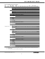
Specifications
Features
• Density: 1G bits
• Organization
— 16M words × 8 bits × 8 banks (EDJ1108EJBG)
— 8M words × 16 bits × 8 banks (EDJ1116EJBG)
• Package
— 78-ball FBGA (EDJ1108EJBG)
— 96-ball FBGA (EDJ1116EJBG)
— Lead-free (RoHS compliant) and Halogen-free
• Power supply: 1.35V (typ)
— VDD = 1.283V to 1.45V
— Backward compatible for VDD, VDDQ
= 1.5V ± 0.075V
• Data rate
— 1866Mbps/1600Mbps/1333Mbps (max)
• 1KB page size (EDJ1108EJBG)
— Row address: A0 to A13
— Column address: A0 to A9
• 2KB page size (EDJ1116EJBG)
— Row address: A0 to A12
— Column address: A0 to A9
• Eight internal banks for concurrent operation
• Burst length (BL): 8 and 4 with Burst Chop (BC)
• Burst type (BT):
— Sequential (8, 4 with BC)
— Interleave (8, 4 with BC)
• /CAS Latency (CL): 5, 6, 7, 8, 9, 10, 11, 13
• /CAS Write Latency (CWL): 5, 6, 7, 8, 9
• Precharge: auto precharge option for each burst
access
• Driver strength: RZQ/7, RZQ/6 (RZQ = 240Ω)
• Refresh: auto-refresh, self-refresh
• Refresh cycles
— Average refresh period
7.8µs at 0°C ≤ TC ≤ +85°C
3.9µs at +85°C < TC ≤ +95°C
• Operating case temperature range
— TC = 0°C to +95°C
• Double-data-rate architecture: two data transfers per
clock cycle
• The high-speed data transfer is realized by the 8 bits
prefetch pipelined architecture
• Bi-directional differential data strobe (DQS and /DQS)
is transmitted/received with data for capturing data at
the receiver
• DQS is edge-aligned with data for READs; centeraligned with data for WRITEs
• Differential clock inputs (CK and /CK)
• DLL aligns DQ and DQS transitions with CK transitions
• Commands entered on each positive CK edge; data
and data mask referenced to both edges of DQS
• Data mask (DM) for write data
• Posted /CAS by programmable additive latency for
better command and data bus efficiency
• On-Die Termination (ODT) for better signal quality
— Synchronous ODT
— Dynamic ODT
— Asynchronous ODT
• Multi Purpose Register (MPR) for pre-defined pattern
read out
• ZQ calibration for DQ drive and ODT
• /RESET pin for Power-up sequence and reset function
• SRT range:
— Normal/extended
• Programmable Output driver impedance control
• Seamless BL4 access with bank-grouping
— Applied only for DDR3-1333 and 1600
Document. No. E1949E11 (Ver. 1.1)
Date Published September 2012 (K) Japan
Printed in Japan
URL: http://www.elpida.com
©Elpida Memory, Inc. 2012
EDJ1108EJBG, EDJ1116EJBG
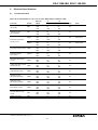
Ordering Information
Die
revision
Part number
Organization
(words × bits)
Internal
banks
JEDEC speed bin
(CL-tRCD-tRP)
78-ball FBGA
96-ball FBGA
Package
EDJ1108EJBG-JS-F
EDJ1108EJBG-GN-F
EDJ1108EJBG-DJ-F
J
128M × 8
8
DDR3L-1866M (13-13-13)
DDR3L-1600K (11-11-11)
DDR3L-1333H (9-9-9)
EDJ1116EJBG-JS-F
EDJ1116EJBG-GN-F
EDJ1116EJBG-DJ-F
J
64M × 16
8
DDR3L-1866M (13-13-13)
DDR3L-1600K (11-11-11)
DDR3L-1333H (9-9-9)
Note: 1.
Please refer to the EDJ1108DJBG, EDJ1116DJBG datasheet (E1729E) when using this device at 1.5V operation, unless
stated otherwise.
Part Number
E D J 11 08 E J BG - JS - F
Elpida Memory
Type
D: Packaged Device
Environment code
F: Lead Free (RoHS compliant)
and Halogen Free
Product Family
J: DDR3
Density / Bank
11: 1Gb / 8-bank
Speed
JS: DDR3-1866M (13-13-13)
GN: DDR3-1600K (11-11-11)
DJ: DDR3-1333H (9-9-9)
Organization
08: x8
16: x16
Package
BG: FBGA
Power Supply
Die Rev.
E: ,1.35V
Operating Frequency
Frequency (Mbps)
Speed
Grade
CL5
CL6
CL7
CL8
CL9
CL10
CL11
CL13
-JS
667
800
1066
1066
1333
1333
1600
1866
-GN
667
800
1066
1066
1333
1333
1600
-DJ
667
800
1066
1066
1333
1333
speed bin
(CL-tRCD-tRP)
DDR3L-1866
(13-13-13)
DDR3L-1600
(11-11-11)
DDR3L-1333
(9-9-9)
Detailed Information
For detailed electrical specification and further information, please refer to the DDR3L SDRAM General Functionality
and Electrical Condition data sheet (E1927E) and Addendum data sheet (E1928E).
Preliminary Data Sheet E1949E11 (Ver. 1.1)
2
EDJ1108EJBG, EDJ1116EJBG
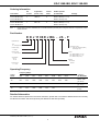
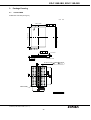
Pin Configurations
Pin Configurations (×8 configuration)
/xxx indicates active low signal.
78-ball FBGA
2
1
3
7
8
9
A
VSS
VDD
NC
NU/(/TDQS) VSS
VDD
B
VSS VSSQ
DQ0
DM/TDQS VSSQ VDDQ
C
VDDQ
DQ2
DQS
DQ1
DQ3
VSSQ
VSSQ
DQ6
/DQS
VDD
VSS
VSSQ
VREFDQ VDDQ
DQ4
DQ7
DQ5
VDDQ
D
E
F
NC
VSS
/RAS
CK
VSS
NC
ODT
VDD
/CAS
/CK
VDD
CKE
NC
/CS
/WE
A10(AP)
ZQ
NC
VSS
BA0
BA2
NC
VDD
A3
A0
VSS
A5
A2
A1
A4
VSS
VDD
A7
A9
A11
A6
VDD
VSS /RESET A13
NC
A8
VSS
G
H
J
VREFCA VSS
K
A12(/BC) BA1
VDD
L
M
N
(Top view)
Pin name
Function
Pin name
Function
A0 to A13*3
Address inputs
A10(AP): Auto precharge
A12(/BC): Burst chop
/RESET*3
Active low asynchronous reset
BA0 to BA2*3
Bank select
VDD
Supply voltage for internal circuit
DQ0 to DQ7
Data input/output
VSS
Ground for internal circuit
DQS, /DQS
Differential data strobe
VDDQ
Supply voltage for DQ circuit
TDQS, /TDQS
Termination data strobe
VSSQ
Ground for DQ circuit
/CS*3
Chip select
VREFDQ
Reference voltage for DQ
/RAS, /CAS, /WE*3
Command input
VREFCA
Reference voltage for CA
CKE*
Reference pin for ZQ calibration
Clock enable
ZQ
CK, /CK
Differential clock input
NC*1
No connection
DM
Write data mask
NU*
Not usable
ODT*3
ODT control
3
Notes: 1.
2.
3.
2
Not internally connected with die.
Don't connect. Internally connected.
Input only pins (address, command, CKE, ODT and /RESET) do not supply termination.
Preliminary Data Sheet E1949E11 (Ver. 1.1)
3
EDJ1108EJBG, EDJ1116EJBG
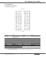
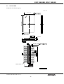
Pin Configurations (× 16 configuration)
/xxx indicates active low signal.
96-ball FBGA
2
1
3
7
8
9
A
VDDQ DQU5 DQU7
DQU4 VDDQ
VSS
VSSQ
/DQSU DQU6 VSSQ
B
VDD
VSS
C
D
VDDQ DQU3 DQU1
DQSU DQU2 VDDQ
VSSQ VDDQ DMU
DQU0 VSSQ
VDD
E
VSS
VSSQ DQL0
DML
VSSQ VDDQ
F
VDDQ DQL2 DQSL
DQL1 DQL3 VSSQ
VSSQ DQL6 /DQSL
VDD
G
VSS
VSSQ
H
DQL7 DQL5 VDDQ
VREFDQ VDDQ DQL4
J
NC
VSS
/RAS
CK
VSS
NC
ODT
VDD
/CAS
/CK
VDD
CKE
NC
/CS
/WE
A10(AP)
ZQ
NC
VSS
BA0
BA2
NC
VDD
A3
A0
VSS
A5
A2
A1
A4
VSS
VDD
A7
A9
A11
A6
VDD
VSS /RESET NC
NC
A8
VSS
K
L
M
VREFCA VSS
N
A12(/BC) BA1
VDD
P
R
T
(Top view)
Pin name
Function
Pin name
Function
A0 to A12*2
Address inputs
A10(AP): Auto precharge
A12(/BC): Burst chop
/RESET*2
Active low asynchronous reset
BA0 to BA2*2
Bank select
VDD
Supply voltage for internal circuit
DQU0 to DQU7
DQL0 to DQL7
Data input/output
VSS
Ground for internal circuit
DQSU, /DQSU
DQSL, /DQSL
Differential data strobe
VDDQ
Supply voltage for DQ circuit
Chip select
VSSQ
Ground for DQ circuit
/CS*2
/RAS, /CAS, /WE*
Command input
VREFDQ
Reference voltage for DQ
CKE*2
Clock enable
VREFCA
Reference voltage for CA
CK, /CK
Differential clock input
ZQ
Reference pin for ZQ calibration
DMU, DML
Write data mask
NC*1
No connection
ODT*2
ODT control
2
Notes: 1.
2.
Not internally connected with die.
Input only pins (address, command, CKE, ODT and /RESET) do not supply termination.
Preliminary Data Sheet E1949E11 (Ver. 1.1)
4
EDJ1108EJBG, EDJ1116EJBG
CONTENTS
Specifications ........................................................................................................................................ 1
Features ................................................................................................................................................ 1
Ordering Information ............................................................................................................................. 2
Part Number .......................................................................................................................................... 2
Operating Frequency ............................................................................................................................ 2
Detailed Information .............................................................................................................................. 2
Pin Configurations ................................................................................................................................. 3
1. Electrical Conditions ...................................................................................................................... 6
1.1
1.2
1.3
1.4
2.
Electrical Specifications ............................................................................................................... 19
2.1
2.2
2.3
3.
DC Characteristics .......................................................................................................................... 19
Pin Capacitance .............................................................................................................................. 21
Standard Speed Bins ...................................................................................................................... 23
Package Drawing ......................................................................................................................... 28
3.1
3.2
4.
Absolute Maximum Ratings ..............................................................................................................6
Operating Temperature Condition ....................................................................................................6
Recommended DC Operating Conditions ........................................................................................7
IDD and IDDQ Measurement Conditions ..........................................................................................8
78-ball FBGA .................................................................................................................................. 28
96-ball FBGA .................................................................................................................................. 29
Recommended Soldering Conditions .......................................................................................... 30
Preliminary Data Sheet E1949E11 (Ver. 1.1)
5
EDJ1108EJBG, EDJ1116EJBG
1.
Electrical Conditions
• All voltages are referenced to VSS (GND)
• Execute power-up and Initialization sequence before proper device operation is achieved.
1.1
Absolute Maximum Ratings
Table 1: Absolute Maximum Ratings
Parameter
Symbol
Rating
Unit
Notes
Power supply voltage
VDD
−0.4 to +1.975
V
1, 3
Power supply voltage for output
VDDQ
−0.4 to +1.975
V
1, 3
Input voltage
VIN
−0.4 to +1.975
V
1
Output voltage
VOUT
−0.4 to +1.975
V
1
Reference voltage
VREFCA
−0.4 to 0.6 × VDD
V
3
Reference voltage for DQ
VREFDQ
−0.4 to 0.6 × VDDQ
V
3
Storage temperature
Tstg
−55 to +100
°C
1, 2
Power dissipation
PD
1.0
W
1
Short circuit output current
IOUT
50
mA
1
Notes: 1.
2.
3.
Stresses greater than those listed under Absolute Maximum Ratings may cause permanent damage to the device. This
is a stress rating only and functional operation of the device at these or any other conditions above those indicated in the
operational sections of this specification is not implied. Exposure to absolute maximum rating conditions for extended
periods may affect reliability.
Storage temperature is the case surface temperature on the center/top side of the DRAM.
VDD and VDDQ must be within 300mV of each other at all times; and VREF must be no greater than 0.6 × VDDQ, When
VDD and VDDQ are less than 500mV; VREF may be equal to or less than 300mV.
Caution: Exposing the device to stress above those listed in Absolute Maximum Ratings could cause
permanent damage. The device is not meant to be operated under conditions outside the limits
described in the operational section of this specification. Exposure to Absolute Maximum Rating
conditions for extended periods may affect device reliability.
1.2
Operating Temperature Condition
Table 2: Operating Temperature Condition
Parameter
Symbol
Rating
Unit
Notes
Operating case temperature
TC
0 to +95
°C
1, 2, 3
Notes: 1.
2.
3.
Operating temperature is the case surface temperature on the center/top side of the DRAM.
The Normal Temperature Range specifies the temperatures where all DRAM specifications will be supported. During
operation, the DRAM case temperature must be maintained between 0°C to +85°C under all operating conditions.
Some applications require operation of the DRAM in the Extended Temperature Range between +85°C and +95°C case
temperature. Full specifications are guaranteed in this range, but the following additional conditions apply:
a) Refresh commands must be doubled in frequency, therefore reducing the refresh interval tREFI to 3.9µs. (This double
refresh requirement may not apply for some devices.)
b) If Self-refresh operation is required in the Extended Temperature Range, then it is mandatory to either use the Manual
Self-Refresh mode with Extended Temperature Range capability (MR2 bit [A6, A7] = [0, 1]) or enable the optional Auto
Self-Refresh mode (MR2 bit [A6, A7] = [1, 0]).
Preliminary Data Sheet E1949E11 (Ver. 1.1)
6
EDJ1108EJBG, EDJ1116EJBG
1.3
Recommended DC Operating Conditions
Table 3: Recommended DC Operating Conditions (TC = 0°C to +85°C), DDR3L Operation
Parameter
Symbol
min.
typ.
max.
Unit
Notes
Supply voltage
VDD
1.283
1.35
1.45
V
1, 2, 3, 4
Supply voltage for DQ
VDDQ
1.283
1.35
1.45
V
1, 2, 3, 4
Notes: 1.
2.
3.
4.
5.
Maximum DC value may not be greater than 1.425V. The DC value is the linear average of VDD/VDDQ(t) over a very
long period of time (e.g. 1 sec).
If maximum limit is exceeded, input levels shall be governed by DDR3 specifications.
Under these supply voltages, the device operates to this DDR3L specifcation.
Once initialized for DDR3L operation, DDR3 operation may only be used if the device is in reset while
VDD and VDDQ are changed for DDR3 operation shown as following timing wave form.
Table 4: Recommended DC Operating Conditions (TC = 0°C to +85°C), DDR3 Operation
Parameter
Symbol
min
typ
max
Supply voltage
VDD
1.425
1.5
1.575
V
1, 2, 3
Supply voltage for DQ
VDDQ
1.425
1.5
1.575
V
1, 2, 3
Notes: 1.
2.
3.
Unit
Notes
If minimum limit is exceeded, input levels shall be governed by DDR3L specifications.
Under 1.5V operation, this DDR3L device operates to the DDR3 specifcations under the same speedtimings as defined
for this device.
Once initialized for DDR3 operation, DDR3L operation may only be used if the device is in reset while VDD and VDDQ
are changed for DDR3L operation shown as below.
Ta
Tb
Tc
Td
Te
Tf
Tg
Th
Ti
Tj
Tk
CK, /CK
tCKSRX
VDD, VDDQ (DDR3)
T(min) = 10ns
VDD, VDDQ (DDR3L)
T(min) = 10ns
T(min) = 200µs
T = 500µs
/RESET
tIS
T(min) = 10ns
CKE
Valid
tDLLK
tXPR
tIS
Command
*1
BA
tMRD
tMRD
tMRD
tMOD
MRS
MRS
MRS
MRS
MR2
MR3
MR1
MR0
tZQinit
ZQCL
*1
Valid
Valid
tIS
ODT
tIS
Static low in case RTT_Nore is enabled at time Tg, otherwise static high or low
Valid
RTT
: VIH or VIL
Note: 1. From time point Td until Tk, NOP or DES commands must be applied between MRS and ZQCL commands.
Figure 1: VDD/VDDQ Voltage Switch between DDR3L and DDR3
Preliminary Data Sheet E1949E11 (Ver. 1.1)
7
EDJ1108EJBG, EDJ1116EJBG
1.4
IDD and IDDQ Measurement Conditions
In this chapter, IDD and IDDQ measurement conditions such as test load and patterns are defined.
The figure Measurement Setup and Test Load for IDD and IDDQ Measurements shows the setup and test load for IDD
and IDDQ measurements.
• IDD currents (such as IDD0, IDD1, IDD2N, IDD2NT, IDD2P0, IDD2P1, IDD2Q, IDD3N, IDD3P, IDD4R, IDD4W,
IDD5B, IDD6, IDD6ET, IDD6TC and IDD7) are measured as time-averaged currents with all VDD balls of the DDR3
SDRAM under test tied together. Any IDDQ current is not included in IDD currents.
• IDDQ currents (such as IDDQ2NT and IDDQ4R) are measured as time-averaged currents with all VDDQ balls of
the DDR3 SDRAM under test tied together. Any IDD current is not included in IDDQ currents.
Note:IDDQ values cannot be directly used to calculate I/O power of the DDR3 SDRAM. They can be used to support
correlation of simulated I/O power to actual I/O power as outlined in correlation from simulated channel I/O
power to actual channel I/O power supported by IDDQ measurement.
For IDD and IDDQ measurements, the following definitions apply:
• L and 0: VIN ≤ VIL(AC)max
• H and 1: VIN ≥ VIH(AC)min
• MID-LEVEL: defined as inputs are VREF = VDDQ / 2
• FLOATING: don't care or floating around VREF.
• Timings used for IDD and IDDQ measurement-loop patterns are provided in Timings used for IDD and IDDQ
Measurement-Loop Patterns table.
• Basic IDD and IDDQ measurement conditions are described in Basic IDD and IDDQ Measurement Conditions
table.
Note:The IDD and IDDQ measurement-loop patterns need to be executed at least one time before actual IDD or
IDDQ measurement is started.
• Detailed IDD and IDDQ measurement-loop patterns are described in IDD0 Measurement-Loop Pattern table
through IDD7 Measurement-Loop Pattern table.
• IDD Measurements are done after properly initializing the DDR3 SDRAM. This includes but is not limited to setting.
RON = RZQ/7 (34Ω in MR1);
Qoff = 0B (Output Buffer enabled in MR1);
RTT_Nom = RZQ/6 (40Ω in MR1);
RTT_WR = RZQ/2 (120Ω in MR2);
TDQS Feature disabled in MR1
• Define D = {/CS, /RAS, /CAS, /WE} : = {H, L, L, L}
• Define /D = {/CS, /RAS, /CAS, /WE} : = {H, H, H, H}
Preliminary Data Sheet E1949E11 (Ver. 1.1)
8
EDJ1108EJBG, EDJ1116EJBG
IDDQ
IDD
VDD
/RESET
CK, /CK
CKE
/CS
/RAS, /CAS, /WE
VDDQ
DDR3
SDRAM
Address, BA
ODT
ZQ
VSS
DQS, /DQS,
DQ, DM,
TDQS, /TDQS
RTT = 25Ω
VDDQ/2
VSSQ
Figure 2: Measurement Setup and Test Load for IDD and IDDQ Measurements
Application specific
memory channel
environment
Channel
I/O power
simulation
IDDQ
Test load
IDDQ
simulation
IDDQ
measurement
Correlation
Correction
Channel I/O power
number
Figure 3: Correlation from Simulated Channel I/O Power to Actual Channel I/O Power
Supported by IDDQ Measurement
Preliminary Data Sheet E1949E11 (Ver. 1.1)
9
EDJ1108EJBG, EDJ1116EJBG
1.4.1
Timings Used for IDD and IDDQ Measurement-Loop Patterns
Table 5: Timings Used for IDD and IDDQ Measurement-Loop Patterns
DDR3-800
DDR3-1066
DDR3-1333
DDR3-1600
Parameter
6-6-6
7-7-7
9-9-9
11-11-11
Unit
CL
6
7
9
11
nCK
tCK(min)
2.5
1.875
1.5
1.25
ns
nRCD(min)
6
7
9
11
nCK
nRC(min)
21
27
33
39
nCK
nRAS(min)
15
20
24
28
nCK
nRP(min)
6
7
9
11
nCK
nFAW (1KB)
16
20
20
24
nCK
nFAW (2KB, 4KB)
20
27
30
32
nCK
nRRD (1KB)
4
4
4
5
nCK
nRRD (2KB, 4KB)
4
6
5
6
nCK
nRFC (1Gb)
44
59
74
88
nCK
nRFC (2Gb)
64
86
107
128
nCK
nRFC (4Gb)
104
139
174
208
nCK
DDR3-1866
Parameter
13-13-13
Unit
CL
13
nCK
tCK(min)
1.07
ns
nRCD(min)
13
nCK
nRC(min)
45
nCK
nRAS(min)
32
nCK
nRP(min)
13
nCK
nFAW (1KB)
26
nCK
nFAW (2KB, 4KB)
33
nCK
nRRD (1KB)
5
nCK
nRRD (2KB, 4KB)
6
nCK
nRFC (1Gb)
103
nCK
nRFC (2Gb)
150
nCK
nRFC (4Gb)
243
nCK
Preliminary Data Sheet E1949E11 (Ver. 1.1)
10
EDJ1108EJBG, EDJ1116EJBG
1.4.2
Basic IDD and IDDQ Measurement Conditions
Table 6: Basic IDD and IDDQ Measurement Conditions
Parameter
Symbol
Description
IDD0
CKE: H; External clock: on; tCK, nRC, nRAS, CL: see Table 5; BL: 8*1; AL: 0; /CS: H
between ACT and PRE; Command, address, bank address inputs: partially toggling
according to Table 7; Data I/O: MID-LEVEL; DM: stable at 0;
Bank activity: cycling with one bank active at a time: 0,0,1,1,2,2,... (see Table 7);
Output buffer and RTT: enabled in MR*2; ODT signal: stable at 0; Pattern details: see
Table 7
IDD1
CKE: H; External clock: On; tCK, nRC, nRAS, nRCD, CL: see Table 5; BL: 8*1, *6; AL:
0; /CS: H between ACT, RD and PRE; Command, address, bank address inputs, data
I/O: partially toggling according to Table 8;
DM: stable at 0; Bank activity: cycling with one bank active at a time: 0,0,1,1,2,2,...
(see Table 8); Output buffer and RTT: enabled in MR*2; ODT Signal: stable at 0;
Pattern details: see Table 8
IDD2N
CKE: H; External clock: on; tCK, CL: see Table 5 BL: 8*1; AL: 0; /CS: stable at 1;
Command, address, bank address Inputs: partially toggling according to Table 9;
data I/O: MID-LEVEL; DM: stable at 0; bank activity: all banks closed; output buffer
and RTT: enabled in mode registers*2; ODT signal: stable at 0; pattern details: see
Table 9
Precharge standby
ODT current
IDD2NT
CKE: H; External clock: on; tCK, CL: see Table 5; BL: 8*1; AL: 0; /CS: stable at 1;
Command, address, bank address Inputs: partially toggling according to Table 10;
data I/O: MID-LEVEL; DM: stable at 0; bank activity: all banks closed; output buffer
and RTT: enabled in MR*2; ODT signal: toggling according to Table 10; pattern
details: see Table 10
Precharge standby
ODT IDDQ current
IDDQ2NT
Same definition like for IDD2NT, however measuring IDDQ current instead of IDD
current
IDD2P0
CKE: L; External clock: on; tCK, CL: see Table 5; BL: 8*1; AL: 0; /CS: stable at 1;
Command, address, bank address inputs: stable at 0; data I/O: MID-LEVEL; DM:
stable at 0; bank activity: all banks closed; output buffer and RTT: EMR*2; ODT
signal: stable at 0; precharge power down mode: slow exit*3
IDD2P1
CKE: L; External clock: on; tCK, CL: see Table 6; BL: 8*1; AL: 0; /CS: stable at 1;
Command, address, bank address Inputs: stable at 0; data I/O: MID-LEVEL;
DM:stable at 0; bank activity: all banks closed; output buffer and RTT: enabled in
MR*2; ODT signal: stable at 0; precharge power down mode: fast exit*3
IDD2Q
CKE: H; External clock: On; tCK, CL: see Table 5; BL: 8*1; AL: 0; /CS: stable at 1;
Command, address, bank address Inputs: stable at 0; data I/O: MID-LEVEL;
DM: stable at 0;bank activity: all banks closed; output buffer and RTT: enabled in
MR*2; ODT signal: stable at 0
IDD3N
CKE: H; External clock: on; tCK, CL: see Table 5; BL: 8*1; AL: 0; /CS: stable at 1;
Command, address, bank address Inputs: partially toggling according to Table 9;
data I/O: MID-LEVEL; DM: stable at 0;
bank activity: all banks open; output buffer and RTT: enabled in MR*2;
ODT signal: stable at 0; pattern details: see Table 9
IDD3P
CKE: L; External clock: on; tCK, CL: see Table 5; BL: 8*1; AL: 0; /CS: stable at 1;
Command, address, bank address inputs: stable at 0; data I/O: MID-LEVEL;
DM:stable at 0; bank activity: all banks open; output buffer and RTT:
enabled in MR*2; ODT signal: stable at 0
Operating burst read
current
IDD4R
CKE: H; External clock: on; tCK, CL: see Table 5; BL: 8*1, *6; AL: 0; /CS: H between
RD; Command, address, bank address Inputs: partially toggling according to
Table 11; data I/O: seamless read
data burst with different data between one burst and the next one according to
Table 11; DM: stable at 0;
bank activity: all banks open, RD commands cycling through banks: 0,0,1,1,2,2,...
(see Table 11); Output buffer and RTT: enabled in MR*2; ODT signal: stable at 0;
pattern details: see Table 11
Operating burst read
IDDQ current
IDDQ4R
Same definition like for IDD4R, however measuring IDDQ current instead of IDD
current
Operating one bank
active precharge
current
Operating one bank
active-read-precharge
current
Precharge standby
current
Precharge power-down
current slow exit
Precharge power-down
current fast exit
Precharge quiet
standby current
Active standby current
Active power-down
current
Preliminary Data Sheet E1949E11 (Ver. 1.1)
11
EDJ1108EJBG, EDJ1116EJBG
Table 6: Basic IDD and IDDQ Measurement Conditions (cont’d)
Parameter
Operating burst write current
Burst refresh current
Self-refresh current: normal
temperature range
Symbol
Description
IDD4W
CKE: H; External clock: on; tCK, CL: see Table 5; BL: 8*1; AL: 0; /CS: H between WR;
command, address, bank address inputs: partially toggling according to Table 12;
data I/O: seamless write data burst with different data between one burst and the next
one according to IDD4W Measurement-Loop Pattern table; DM: stable at 0; bank
activity: all banks open,
WR commands cycling through banks: 0,0,1,1,2,2,.. (see Table 12); Output buffer
and RTT: enabled in MR*2; ODT signal: stable
at H; pattern details: see Table 12
IDD5B
CKE: H; External clock: on; tCK, CL, nRFC: see Table 5; BL: 8*1; AL: 0; /CS: H
between REF;
Command, address, bank address Inputs: partially toggling according to Table 13;
data I/O: MID-LEVEL; DM: stable at 0;
bank activity: REF command every nRFC (Table 13); output buffer and RTT: enabled
in MR*2; ODT signal: stable at 0; pattern
details: see Table 13
IDD6
TC: 0 to 85°C; ASR: disabled*4; SRT:
Normal*5; CKE: L; External clock: off; CK and /CK: L; CL: see Table 5; BL: 8*1;
AL: 0; /CS, command, address, bank address, data I/O: MID-LEVEL; DM: stable
at 0; bank activity: Self-refresh operation; output buffer and RTT: enabled in MR*2;
ODT signal: MID-LEVEL
Self-refresh current: extended
IDD6ET
temperature range
TC: 0 to 95°C; ASR: Disabled*4; SRT: Extended*5; CKE: L; External clock: off; CK
and /CK: L; CL: Table 5; BL: 8*1; AL: 0; /CS, command, address, bank address, data
I/O: MID-LEVEL;
DM: stable at 0; bank activity: Extended temperature self-refresh operation; output
buffer and RTT: enabled in MR*2; ODT signal: MID-LEVEL
Auto self-refresh current
(Optional)
IDD6TC
TC: 0 to 95°C; ASR: Enabled*4; SRT: Normal*5; CKE: L; External clock: off;
CK and /CK: L; CL: Table 5; BL: 8*1; AL: 0; /CS, command, address, bank address,
data I/O: MID-LEVEL; DM: stable at 0; bank activity: Auto self-refresh operation;
output buffer and RTT: enabled in MR*2; ODT signal: MID-LEVEL
IDD7
CKE: H; External clock: on; tCK, nRC, nRAS, nRCD, nRRD, nFAW, CL: see Table 5;
BL: 8*1, *6; AL: CL-1; /CS: H between ACT and RDA; Command, address, bank
address Inputs: partially toggling according to Table 14; data I/O: read data bursts
with different data between one burst and the next one according to Table 14; DM:
stable at 0; bank activity: two times interleaved cycling through banks (0, 1, …7) with
different addressing, see Table 14; output buffer and RTT: enabled in MR*2; ODT
signal: stable at 0; pattern details: see Table 14
IDD8
/RESET: low; External clock: off; CK and /CK: low; CKE: FLOATING; /CS, command,
address, bank address, Data IO: FLOATING; ODT signal: FLOATING
RESET low current reading is valid once power is stable and /RESET has been low
for at least 1ms.
Operating bank interleave
read current
RESET low current
Notes: 1.
2.
3.
4.
5.
6.
Burst Length: BL8 fixed by MRS: MR0 bits [1,0] = [0,0].
MR: Mode Register
Output buffer enable: set MR1 bit A12 = 1 and MR1 bits [5, 1] = [0,1];
RTT_Nom enable: set MR1 bits [9, 6, 2] = [0, 1, 1]; RTT_WR enable: set MR2 bits [10, 9] = [1,0].
Precharge power down mode: set MR0 bit A12= 0 for Slow Exit or MR0 bit A12 = 1 for fast exit.
Auto self-refresh (ASR): set MR2 bit A6 = 0 to disable or 1 to enable feature.
Self-refresh temperature range (SRT): set MR0 bit A7= 0 for normal or 1 for extended temperature range.
Read burst type: nibble sequential, set MR0 bit A3 = 0
Preliminary Data Sheet E1949E11 (Ver. 1.1)
12
EDJ1108EJBG, EDJ1116EJBG
Table 7: IDD0 Measurement-Loop Pattern
CK,
/CK
CKE
Sub
Cycle
-Loop number
0
Toggling Static H
Notes: 1.
2.
3.
4.
Command /CS
/RAS /CAS /WE
ODT
A11
BA*3 -Am
A10
A7
-A9
A3
-A6
A0
-A2
0
ACT
0
0
1
1
0
0
0
0
0
0
0
1, 2
D, D
1
0
0
0
0
0
0
0
0
0
0
3, 4
/D, /D 1
1
1
1
0
0
0
0
0
0
0
0
0
0
0
…
Repeat pattern 1…4 until nRAS − 1, truncate if necessary
nRAS
PRE
…
Repeat pattern 1...4 until nRC − 1, truncate if necessary
1 × nRC
+0
ACT
0
0
1
1
0
0
0
0
0
F
0
1 × nRC
+1, 2
D, D
1
0
0
0
0
0
0
0
0
F
0
1 × nRC
+ 3, 4
/D, /D 1
1
1
1
0
0
0
0
0
F
0
0
0
1
0
0
0
0
…
Repeat pattern nRC + 1,...,4 until 1 × nRC + nRAS − 1, truncate if necessary
1 × nRC
+ nRAS
PRE
0
0
1
0
0
0
0
0
…
Repeat nRC + 1,...,4 until 2 × nRC − 1, truncate if necessary
1
2 × nRC
Repeat Sub-Loop 0, use BA= 1 instead
2
4 × nRC
Repeat Sub-Loop 0, use BA= 2 instead
3
6 × nRC
Repeat Sub-Loop 0, use BA= 3 instead
4
8 × nRC
Repeat Sub-Loop 0, use BA= 4 instead
5
10 × nRC Repeat Sub-Loop 0, use BA= 5 instead
6
12 × nRC Repeat Sub-Loop 0, use BA= 6 instead
7
14 × nRC Repeat Sub-Loop 0, use BA= 7 instead
DM must be driven low all the time. DQS, /DQS are MID-LEVEL.
DQ signals are MID-LEVEL.
BA: BA0 to BA2.
Am: m means Most Significant Bit (MSB) of Row address.
Preliminary Data Sheet E1949E11 (Ver. 1.1)
13
0
F
0
Data*2
EDJ1108EJBG, EDJ1116EJBG
Table 8: IDD1 Measurement-Loop Pattern
CK,
/CK
CKE
Sub
Cycle
-Loop number
0
Toggling Static H
Notes: 1.
2.
3.
4.
Command /CS
/RAS /CAS /WE
ODT
A11
BA*3 -Am
A10
A7 A3 A0
-A9 -A6 -A2 Data*2
0
ACT
0
0
1
1
0
0
0
0
0
0
0
⎯
1, 2
D, D
1
0
0
0
0
0
0
0
0
0
0
⎯
3, 4
/D, /D 1
1
1
1
0
0
0
0
0
0
0
⎯
0
0
0
0
00000000
0
0
0
0
⎯
…
Repeat pattern 1...4 until nRCD − 1, truncate if necessary
nRCD
RD
…
Repeat pattern 1...4 until nRAS − 1, truncate if necessary
nRAS
PRE
…
Repeat pattern 1...4 until nRC − 1, truncate if necessary
1 × nRC
+0
ACT
0
0
1
1
0
0
0
0
0
F
0
⎯
1 × nRC
+ 1, 2
D, D
1
0
0
0
0
0
0
0
0
F
0
⎯
1 × nRC
+ 3, 4
/D, /D 1
1
1
1
0
0
0
0
0
F
0
⎯
0
00110011
0
⎯
0
0
1
0
0
1
1
0
0
0
0
0
0
0
…
Repeat pattern nRC + 1,..., 4 until nRC + nRCD − 1, truncate if necessary
1 × nRC
+ nRCD
RD
…
Repeat pattern nRC + 1,..., 4 until nRC +nRAS − 1, truncate if necessary
1 × nRC
+ nRAS
PRE
0
0
1
0
0
1
1
0
0
0
0
0
0
0
0
0
0
0
…
Repeat pattern nRC + 1,..., 4 until 2 × nRC − 1, truncate if necessary
1
2 × nRC
Repeat Sub-Loop 0, use BA= 1 instead
2
4 × nRC
Repeat Sub-Loop 0, use BA= 2 instead
3
6 × nRC
Repeat Sub-Loop 0, use BA= 3 instead
4
8 × nRC
Repeat Sub-Loop 0, use BA= 4 instead
5
10 × nRC Repeat Sub-Loop 0, use BA= 5 instead
6
12 × nRC Repeat Sub-Loop 0, use BA= 6 instead
7
14 × nRC Repeat Sub-Loop 0, use BA= 7 instead
F
F
DM must be driven low all the time. DQS, /DQS are used according to read commands, otherwise MID-LEVEL.
Burst sequence driven on each DQ signal by read command. Outside burst operation, DQ signals are MID-LEVEL.
BA: BA0 to BA2.
Am: m means Most Significant Bit (MSB) of Row address.
Preliminary Data Sheet E1949E11 (Ver. 1.1)
14
EDJ1108EJBG, EDJ1116EJBG
Table 9: IDD2N and IDD3N Measurement-Loop Pattern
CK,
/CK
CKE
Sub
Cycle
-Loop number
0
/RAS /CAS /WE
ODT
A11
BA*3 -Am
A10
A7
-A9
A3
-A6
A0
-A2
0
D
1
0
0
0
0
0
0
0
0
0
0
1
D
1
0
0
0
0
0
0
0
0
0
0
2
/D
1
1
1
1
0
0
0
0
0
F
0
1
1
1
1
0
0
0
0
0
F
0
3
/D
4 to 7
Repeat Sub-Loop 0, use BA= 1 instead
8 to 11
Repeat Sub-Loop 0, use BA= 2 instead
3
12 to 15
Repeat Sub-Loop 0, use BA= 3 instead
4
16 to 19
Repeat Sub-Loop 0, use BA= 4 instead
5
20 to 23
Repeat Sub-Loop 0, use BA= 5 instead
6
24 to 27
Repeat Sub-Loop 0, use BA= 6 instead
7
28 to 31
Repeat Sub-Loop 0, use BA= 7 instead
1
Toggling Static H 2
Notes: 1.
2.
3.
4.
Command /CS
Data*2
DM must be driven low all the time. DQS, /DQS are MID-LEVEL.
DQ signals are MID-LEVEL.
BA: BA0 to BA2.
Am: m means Most Significant Bit (MSB) of Row address.
Table 10: IDD2NT and IDDQ2NT Measurement-Loop Pattern
CK,
/CK
CKE
Sub
Cycle
-Loop number
0
/RAS /CAS /WE
ODT
A11
BA*3 -Am
A10
A7
-A9
A3
-A6
A0
-A2
0
D
1
0
0
0
0
0
0
0
0
0
0
1
D
1
0
0
0
0
0
0
0
0
0
0
2
/D
1
1
1
1
0
0
0
0
0
F
0
1
1
1
1
0
0
0
0
0
F
0
3
/D
4 to 7
Repeat Sub-Loop 0, but ODT = 0 and BA= 1
8 to 11
Repeat Sub-Loop 0, but ODT = 1 and BA= 2
3
12 to 15
Repeat Sub-Loop 0, but ODT = 1 and BA= 3
4
16 to 19
Repeat Sub-Loop 0, but ODT = 0 and BA= 4
5
20 to 23
Repeat Sub-Loop 0, but ODT = 0 and BA= 5
6
24 to 27
Repeat Sub-Loop 0, but ODT = 1 and BA= 6
7
28 to 31
Repeat Sub-Loop 0, but ODT = 1 and BA= 7
1
Toggling Static H 2
Notes: 1.
2.
3.
4.
Command /CS
DM must be driven low all the time. DQS, /DQS are MID-LEVEL.
DQ signals are MID-LEVEL.
BA: BA0 to BA2.
Am: m means Most Significant Bit (MSB) of Row address.
Preliminary Data Sheet E1949E11 (Ver. 1.1)
15
Data*2
EDJ1108EJBG, EDJ1116EJBG
Table 11: IDD4R and IDDQ4R Measurement-Loop Pattern
CK,
/CK
CKE
Sub
Cycle
-Loop number
0
Toggling Static H 1
Notes: 1.
2.
3.
4.
Command /CS
/RAS /CAS /WE
ODT
A11
BA*3 -Am
A7
A10 -A9
A3
-A6
A0
-A2
Data*2
0
RD
0
1
0
1
0
0
0
0
0
0
0
00000000
1
D
1
0
0
0
0
0
0
0
0
0
0
⎯
2,3
/D, /D 1
1
1
1
0
0
0
0
0
0
0
⎯
4
RD
0
1
0
1
0
0
0
0
0
F
0
00110011
5
D
1
0
0
0
0
0
0
0
0
F
0
⎯
6,7
/D, /D 1
1
1
1
0
0
0
0
0
F
0
⎯
8 to 15
Repeat Sub-Loop 0, but BA= 1
2
16 to 23
Repeat Sub-Loop 0, but BA= 2
3
24 to 31
Repeat Sub-Loop 0, but BA= 3
4
32 to 39
Repeat Sub-Loop 0, but BA= 4
5
40 to 47
Repeat Sub-Loop 0, but BA= 5
6
48 to 55
Repeat Sub-Loop 0, but BA= 6
7
56 to 63
Repeat Sub-Loop 0, but BA= 7
DM must be driven low all the time. DQS, /DQS are used according to read commands, otherwise MID-LEVEL.
Burst sequence driven on each DQ signal by read command. Outside burst operation, DQ signals are MID-LEVEL.
BA: BA0 to BA2.
Am: m means Most Significant Bit (MSB) of Row address.
Preliminary Data Sheet E1949E11 (Ver. 1.1)
16
EDJ1108EJBG, EDJ1116EJBG
Table 12: IDD4W Measurement-Loop Pattern
CK,
/CK
CKE
Sub
Cycle
-Loop number
0
Toggling Static H 1
Notes: 1.
2.
3.
4.
Command /CS
/RAS /CAS /WE
ODT
A11
BA*3 -Am
A7
A10 -A9
A3
-A6
A0
-A2
Data*2
0
WR
0
1
0
0
1
0
0
0
0
0
0
00000000
1
D
1
0
0
0
1
0
0
0
0
0
0
⎯
2,3
/D, /D 1
1
1
1
1
0
0
0
0
0
0
⎯
4
WR
0
1
0
0
1
0
0
0
0
F
0
00110011
5
D
1
0
0
0
1
0
0
0
0
F
0
⎯
6,7
/D, /D 1
1
1
1
1
0
0
0
0
F
0
⎯
8 to 15
Repeat Sub-Loop 0, but BA= 1
2
16 to 23
Repeat Sub-Loop 0, but BA= 2
3
24 to 31
Repeat Sub-Loop 0, but BA= 3
4
32 to 39
Repeat Sub-Loop 0, but BA= 4
5
40 to 47
Repeat Sub-Loop 0, but BA= 5
6
48 to 55
Repeat Sub-Loop 0, but BA= 6
7
56 to 63
Repeat Sub-Loop 0, but BA= 7
DM must be driven low all the time. DQS, /DQS are used according to write commands, otherwise MID-LEVEL.
Burst sequence driven on each DQ signal by write command. Outside burst operation, DQ signals are MID-LEVEL.
BA: BA0 to BA2.
Am: m means Most Significant Bit (MSB) of Row address.
Table 13: IDD5B Measurement-Loop Pattern
CK,
/CK
CKE
Sub
Cycle
-Loop number
Command /CS
/RAS /CAS /WE
ODT
A11
BA*3 -Am
A7
A10 -A9
A3
-A6
A0
-A2
Data*2
REF
0
0
0
1
0
0
0
0
0
0
0
⎯
1, 2
D
1
0
0
0
0
0
0
0
0
0
0
⎯
3,4
/D, /D 1
1
1
1
0
0
0
0
0
F
0
⎯
5 to 8
Repeat cycles 1...4, but BA= 1
0
0
Toggling Static H
1
2
Notes: 1.
2.
3.
4.
9 to 12
Repeat cycles 1...4, but BA= 2
13 to 16
Repeat cycles 1...4, but BA= 3
17 to 20
Repeat cycles 1...4, but BA= 4
21 to 24
Repeat cycles 1...4, but BA= 5
25 to 28
Repeat cycles 1...4, but BA= 6
29 to 32
Repeat cycles 1...4, but BA= 7
33 to
Repeat Sub-Loop 1, until nRFC − 1. Truncate, if necessary.
nRFC − 1
DM must be driven low all the time. DQS, /DQS are MID-LEVEL.
DQ signals are MID-LEVEL.
BA: BA0 to BA2.
Am: m means Most Significant Bit (MSB) of Row address.
Preliminary Data Sheet E1949E11 (Ver. 1.1)
17
EDJ1108EJBG, EDJ1116EJBG
Table 14: IDD7 Measurement-Loop Pattern
CK,
/CK
CKE
Sub
Cycle
-Loop number
0
/CS
/RAS /CAS /WE ODT
A11
BA*3 -Am
A7 A3 A0
A10 -A9 -A6 -A2 Data*2
0
ACT
0
0
1
1
0
0
0
0
0
0
0
⎯
1
RDA
0
1
0
1
0
0
0
1
0
0
0
00000000
2
D
1
0
0
0
0
0
0
0
0
0
0
⎯
…
Repeat above D Command until nRRD − 1
nRRD
ACT
0
0
1
1
0
1
0
0
0
F
0
⎯
nRRD + 1
RDA
0
1
0
1
0
1
0
1
0
F
0
00110011
nRRD + 2
D
1
0
0
0
0
1
0
0
0
F
0
⎯
…
Repeat above D Command until 2 × nRRD − 1
2
2 × nRRD
Repeat Sub-Loop 0, but BA= 2
3
3 × nRRD
0
0
0
F
0
⎯
0
⎯
1
Repeat Sub-Loop 1, but BA= 3
D
1
0
0
0
0
3
4
4 × nRRD
5
nFAW
Repeat Sub-Loop 0, but BA= 4
6
nFAW
+ nRRD
Repeat Sub-Loop 1, but BA= 5
7
nFAW
Repeat Sub-Loop 0, but BA= 6
+ 2 × nRRD
8
nFAW
Repeat Sub-Loop 1, but BA= 7
+ 3 × nRRD
9
D
1
0
0
0
0
7
0
0
0
F
nFAW
+ 4 × nRRD Assert and repeat above D Command until 2 × nFAW − 1, if necessary
Toggling Static H 10
ACT
0
0
1
1
0
0
0
0
0
F
0
⎯
2 × nFAW
+1
RDA
0
1
0
1
0
0
0
1
0
F
0
00110011
D
1
0
0
0
0
0
0
0
0
F
0
⎯
2 × nFAW
+ nRRD
11
Assert and repeat above D Command until nFAW − 1, if necessary
2 × nFAW
+0
2 × nFAW
+2
Notes: 1.
2.
3.
4.
Command
Repeat above D Command until 2 × nFAW + nRRD − 1
ACT
0
0
1
1
0
1
0
0
0
0
0
⎯
2 × nFAW
RDA
+ nRRD + 1
0
1
0
1
0
1
0
1
0
0
0
00000000
1
0
0
0
0
1
0
0
2 × nFAW D
+ nRRD + 2 Repeat above D Command until 2 × nFAW + 2 × nRRD − 1
0
0
0
⎯
0
⎯
0
⎯
12
2 × nFAW
Repeat Sub-Loop 10, but BA= 2
+2 × nRRD
13
2 × nFAW
Repeat Sub-Loop 11, but BA= 3
+ 3 × nRRD
14
1
0
0
0
0
3
0
0
0
0
2 × nFAW D
+ 4 × nRRD Assert and repeat above D Command until 3 × nFAW − 1, if necessary
15
3 × nFAW
Repeat Sub-Loop 10, but BA= 4
16
3 × nFAW
+nRRD
Repeat Sub-Loop 11, but BA= 5
17
3 × nFAW
Repeat Sub-Loop 10, but BA= 6
+ 2 × nRRD
18
3 × nFAW
Repeat Sub-Loop 11, but BA= 7
+ 3 × nRRD
19
1
0
0
0
0
7
0
0
0
0
3 × nFAW D
+ 4 × nRRD Assert and repeat above D Command until 4 × nFAW − 1, if necessary
DM must be driven low all the time. DQS, /DQS are used according to read commands, otherwise MID-LEVEL.
Burst sequence driven on each DQ signal by read command. Outside burst operation, DQ signals are MID-LEVEL.
BA: BA0 to BA2.
Am: m means Most Significant Bit (MSB) of Row address.
Preliminary Data Sheet E1949E11 (Ver. 1.1)
18
EDJ1108EJBG, EDJ1116EJBG
2.
2.1
Electrical Specifications
DC Characteristics
Table 15: DC Characteristics 1 (TC = 0°C to +85°C, VDD, VDDQ = 1.283V to 1.45V)
Data rate
×8
× 16
Parameter
Symbol
(Mbps)
max
max
Unit
Operating current
(ACT-PRE)
IDD0
1333
1600
1866
48
52
TBD
55
60
TBD
mA
Operating current
(ACT-RD-PRE)
IDD1
1333
1600
1866
60
65
TBD
70
75
TBD
mA
IDD2P1
1333
1600
1866
20
20
TBD
20
20
TBD
mA
Fast PD Exit
IDD2P0
1333
1600
1866
10
10
TBD
10
10
TBD
mA
Slow PD Exit
Precharge standby current
IDD2N
1333
1600
1866
30
30
TBD
30
30
TBD
mA
Precharge standby
ODT current
IDD2NT
1333
1600
1866
30
32
TBD
30
32
TBD
mA
Precharge quiet standby
current
IDD2Q
1333
1600
1866
30
30
TBD
30
30
TBD
mA
Active power-down current
IDD3P
(Always fast exit)
1333
1600
1866
25
25
TBD
25
26
TBD
mA
Active standby current
IDD3N
1333
1600
1866
40
45
TBD
40
45
TBD
mA
Operating current
(Burst read operating)
IDD4R
1333
1600
1866
90
105
TBD
105
120
TBD
mA
Operating current
(Burst write operating)
IDD4W
1333
1600
1866
100
115
TBD
135
155
TBD
mA
Burst refresh current
IDD5B
1333
1600
1866
135
140
TBD
135
140
TBD
mA
All bank interleave read
current
IDD7
1333
1600
1866
160
160
TBD
165
190
TBD
mA
RESET low current
IDD8
10
10
mA
Precharge power-down
standby current
Preliminary Data Sheet E1949E11 (Ver. 1.1)
19
Notes
EDJ1108EJBG, EDJ1116EJBG
Table 16: Self-Refresh Current (TC = 0°C to +85°C, VDD, VDDQ = 1.283V to 1.45V)
Parameter
Symbol
max
Unit
Self-refresh current
normal temperature range
IDD6
10
mA
Self-refresh current
extended temperature range
IDD6ET
12
mA
Auto self-refresh current
(Optional)
IDD6TC
⎯
mA
Preliminary Data Sheet E1949E11 (Ver. 1.1)
20
Notes
EDJ1108EJBG, EDJ1116EJBG
2.2
Pin Capacitance
Table 17: Pin Capacitance [DDR3-800 to 1600] (TC = 25°C, VDD, VDDQ = 1.283V to 1.45V)
DDR3L-800
DDR3L-1066
DDR3L-1333
DDR3L-1600
Min
Max
Min
Max
Min
Max
Min
Max
Units Notes
Input/output capacitance CIO
1.4
2.5
1.4
2.5
1.4
2.3
1.4
2.2
pF
1, 2
Input capacitance,
CK and /CK
0.8
1.6
0.8
1.6
0.8
1.4
0.8
1.4
pF
2
Input capacitance delta,
CDCK
CK and /CK
0
0.15
0
0.15
0
0.15
0
0.15
pF
2, 3
Input/output capacitance
delta,
CDDQS
DQS and /DQS
0
0.2
0
0.2
0
0.15
0
0.15
pF
2, 4
Input capacitance,
(control, address,
command, input-only
pins)
0.75
1.3
0.75
1.3
0.75
1.3
0.75
1.2
pF
2, 5
Input capacitance delta,
(All control input-only
CDI_CTRL −0.5
pins)
0.3
−0.5
0.3
−0.4
0.2
−0.4
0.2
pF
2, 6, 7
Input capacitance delta,
CDI_ADD_
−0.5
(All addres/command
CMD
input-only pins)
0.5
−0.5
0.5
−0.4
0.4
−0.4
0.4
pF
2, 8, 9
Input/output capacitance
delta, DQ,DM, DQS,
CDIO
/DQS, TDQS, /TDQS
−0.5
0.3
−0.5
0.3
−0.5
0.3
−0.5
0.3
pF
2, 10
Input/output capacitance
CZQ
of ZQ pin
⎯
3
⎯
3
⎯
3
⎯
3
pF
2, 11
Parameter
Symbol
CCK
CI
Table 18: Pin Capacitance [DDR3-1866 to 2133] (TC = 25°C, VDD, VDDQ = 1.283V to 1.45V)
DDR3L-1866
Parameter
Symbol
Min
Max
Units
Notes
Input/output capacitance
CIO
1.4
2.1
pF
1, 2
Input capacitance,
CK and /CK
CCK
0.8
1.3
pF
2
Input capacitance delta, CK and /CK CDCK
0
0.15
pF
2, 3
Input/output capacitance delta,
DQS and /DQS
CDDQS
0
0.15
pF
2, 4
Input capacitance,
(control, address, command, inputonly pins)
CI
0.75
1.2
pF
2, 5
Input capacitance delta,
(All control input-only pins)
CDI_CTRL
−0.4
0.2
pF
2, 6, 7
Input capacitance delta, (All
addres/command input-only pins)
CDI_ADD_CMD
−0.4
0.4
pF
2, 8, 9
Input/output capacitance delta,
CDIO
DQ,DM, DQS, /DQS, TDQS, /TDQS
−0.5
0.3
pF
2, 10
Input/output capacitance of ZQ pin
⎯
3
pF
2, 11
Notes: 1.
2.
CZQ
Although the DM, TDQS and /TDQS pins have different functions, the loading matches DQ and DQS.
VDD, VDDQ, VSS, VSSQ applied and all other pins floating (except the pin under test, CKE, /RESET and ODT as
necessary). VDD = VDDQ = 1.35V, VBIAS=VDD/2 and ondie termination off.
Preliminary Data Sheet E1949E11 (Ver. 1.1)
21
EDJ1108EJBG, EDJ1116EJBG
3.
4.
5.
6.
7.
8.
9.
10.
11.
Absolute value of CCK-C/CK.
Absolute value of CIO(DQS)-CIO(/DQS).
CI applies to ODT, /CS, CKE, A0-A15, BA0-BA2, /RAS, /CAS and /WE.
CDI_CTRL applies to ODT, /CS and CKE.
CDI_CTRL = CI(CTRL) − 0.5 × (CI(CK)+CI(/CK)).
CDI_ADD_CMD applies to A0-A15, BA0-BA2, /RAS, /CAS and /WE.
CDI_ADD_CMD = CI(ADD_CMD) − 0.5 × (CI(CK)+CI(/CK)).
CDIO=CIO(DQ,DM) − 0.5 × (CIO(DQS)+CIO(/DQS)).
Maximum external load capacitance on ZQ pin: 5pF.
Preliminary Data Sheet E1949E11 (Ver. 1.1)
22
EDJ1108EJBG, EDJ1116EJBG
2.3
Standard Speed Bins
Table 19: DDR3-800 Speed Bins
Speed Bin
DDR3-800E
CL-tRCD-tRP
6-6-6
Symbol
min
max
Unit
Notes
tAA
/CAS write latency
15
20
ns
10
tRCD
15
⎯
ns
10
tRP
15
⎯
ns
10
tRC
52.5
⎯
ns
10
37.5
9 × tREFI
ns
9
tCK(avg) @CL=5
CWL = 5
3.0
3.3
ns
1, 2, 3, 11
tCK(avg) @CL=6
CWL = 5
2.5
3.3
ns
1, 2, 3, 11
tRAS
Supported CL settings
Supported CWL settings
5, 6
nCK
5
nCK
Table 20: DDR3-1066 Speed Bins
Speed Bin
DDR3-1066F
CL-tRCD-tRP
7-7-7
Symbol
/CAS write latency
tAA
min
max
Unit
Notes
13.125
20
ns
10
tRCD
13.125
⎯
ns
10
tRP
13.125
⎯
ns
10
tRC
50.625
⎯
ns
10
37.5
9 × tREFI
ns
9
CWL = 5
3.0
3.3
ns
1, 2, 3, 4, 5, 11
CWL = 6
Reserved
Reserved
ns
4
CWL = 5
2.5
3.3
ns
1, 2, 3, 5
CWL = 6
Reserved
Reserved
ns
4
CWL = 5
Reserved
Reserved
ns
4
CWL = 6
1.875
< 2.5
ns
1, 2, 3, 4
CWL = 5
Reserved
Reserved
ns
4
CWL = 6
1.875
< 2.5
ns
1, 2, 3
tRAS
tCK(avg) @CL=5
tCK(avg) @CL=6
tCK(avg) @CL=7
tCK(avg) @CL=8
Supported CL settings
Supported CWL settings
Preliminary Data Sheet E1949E11 (Ver. 1.1)
23
5, 6, 7, 8
nCK
5, 6
nCK
EDJ1108EJBG, EDJ1116EJBG
Table 21: DDR3-1333 Speed Bins
Speed Bin
DDR3-1333H
CL-tRCD-tRP
9-9-9
Symbol
min
max
Unit
Notes
tAA
13.5
(13.125)
20
ns
10
tRCD
13.5
(13.125)
⎯
ns
10
tRP
13.5
(13.125)
⎯
ns
10
tRC
49.5
(49.125)
⎯
ns
10
tRAS
36
9 × tREFI
ns
9
CWL = 5
3.0
3.3
ns
1, 2, 3, 4, 6, 11
CWL = 6, 7
Reserved
Reserved
ns
4
CWL = 5
2.5
3.3
ns
1, 2, 3, 6
CWL = 6
Reserved
Reserved
ns
4
CWL = 7
Reserved
Reserved
ns
4
CWL = 5
Reserved
Reserved
ns
4
CWL = 6
1.875
< 2.5
ns
1, 2, 3, 4, 6
CWL = 7
Reserved
Reserved
ns
4
CWL = 5
Reserved
Reserved
ns
4
CWL = 6
1.875
< 2.5
ns
1, 2, 3, 6
CWL = 7
Reserved
Reserved
ns
4
CWL = 5, 6
Reserved
Reserved
ns
4
CWL= 7
1.5
< 1.875
ns
1, 2, 3, 4
CWL = 5, 6
Reserved
Reserved
ns
4
CWL= 7
1.5
< 1.875
ns
1, 2, 3
tCK(avg) @CL=5
tCK(avg) @CL=6
tCK(avg) @CL=7
tCK(avg) @CL=8
tCK(avg) @CL=9
tCK(avg) @CL=10
/CAS write latency
Supported CL settings
Supported CWL settings
Preliminary Data Sheet E1949E11 (Ver. 1.1)
24
5, 6, 7, 8, 9, 10
nCK
5, 6, 7
nCK
EDJ1108EJBG, EDJ1116EJBG
Table 22: DDR3-1600 Speed Bins
Speed Bin
DDR3-1600K
CL-tRCD-tRP
Symbol
11-11-11
min
max
Unit
Notes
tAA
13.75
(13.125)
20
ns
10
tRCD
13.75
(13.125)
⎯
ns
10
tRP
13.75
(13.125)
⎯
ns
10
tRC
48.75
(48.125)
⎯
ns
10
tRAS
35
9 × tREFI
ns
9
tCK(avg) @CL=5
tCK(avg) @CL=6
tCK(avg) @CL=7
tCK(avg) @CL=8
tCK(avg) @CL=9
tCK(avg) @CL=10
tCK(avg) @CL=11
/CAS write latency
CWL = 5
3.0
3.3
ns
1, 2, 3, 4, 7, 11
CWL = 6, 7, 8
Reserved
Reserved
ns
4
CWL = 5
2.5
3.3
ns
1, 2, 3, 7
CWL = 6
Reserved
Reserved
ns
4
CWL = 7, 8
Reserved
Reserved
ns
4
CWL = 5
Reserved
Reserved
ns
4
CWL = 6
1.875
< 2.5
ns
1, 2, 3, 4, 7
CWL = 7
Reserved
Reserved
ns
4
CWL = 8
Reserved
Reserved
ns
4
CWL = 5
Reserved
Reserved
ns
4
CWL = 6
1.875
< 2.5
ns
1, 2, 3, 7
CWL = 7
Reserved
Reserved
ns
4
CWL = 8
Reserved
Reserved
ns
4
CWL = 5, 6
Reserved
Reserved
ns
4
CWL= 7
1.5
< 1.875
ns
1, 2, 3, 4, 7
CWL= 8
Reserved
Reserved
ns
4
CWL = 5, 6
Reserved
Reserved
ns
4
CWL= 7
1.5
< 1.875
ns
1, 2, 3, 7
CWL= 8
Reserved
Reserved
ns
4
CWL = 5, 6, 7
Reserved
Reserved
ns
4
CWL= 8
1.25
< 1.5
ns
1, 2, 3
Supported CL settings
Supported CWL settings
Preliminary Data Sheet E1949E11 (Ver. 1.1)
25
5, 6, 7, 8, 9, 10, 11
nCK
5, 6, 7, 8
nCK
EDJ1108EJBG, EDJ1116EJBG
Table 23: DDR3-1866 Speed Bins
Speed Bin
DDR3-1866M
CL-tRCD-tRP
Symbol
13-13-13
/CAS write latency
min
max
Unit
tAA
13.91
20.0
ns
tRCD
13.91
⎯
ns
tRP
13.91
⎯
ns
tRC
47.91
⎯
ns
tRAS
34.0
9 × tREFI
ns
tCK(avg) @CL=5
tCK(avg) @CL=6
tCK(avg) @CL=7
tCK(avg) @CL=8
tCK(avg) @CL=9
tCK(avg) @CL=10
tCK(avg) @CL=11
tCK(avg) @CL=12
tCK(avg) @CL=13
Notes
9
CWL = 5
3.0
3.3
ns
1, 2, 3, 8
CWL = 6, 7, 8, 9
Reserved
Reserved
ns
4
CWL = 5
2.5
3.3
ns
1, 2, 3, 8
CWL = 6
Reserved
Reserved
ns
4
CWL = 7, 8, 9
Reserved
Reserved
ns
4
CWL = 5
Reserved
Reserved
ns
4
CWL = 6
1.875
2.5
ns
1, 2, 3, 8
CWL = 7, 8, 9
Reserved
Reserved
ns
4
CWL = 5
Reserved
Reserved
ns
4
CWL = 6
1.875
2.5
ns
1, 2, 3, 8
CWL = 7
Reserved
Reserved
ns
4
CWL = 8, 9
Reserved
Reserved
ns
4
CWL = 5, 6
Reserved
Reserved
ns
4
CWL= 7
1.5
1.875
ns
1, 2, 3, 8
CWL= 8
Reserved
Reserved
ns
4
CWL= 9
Reserved
Reserved
ns
4
CWL = 5, 6
Reserved
Reserved
ns
4
CWL= 7
1.5
1.875
ns
1, 2, 3, 8
CWL= 8
Reserved
Reserved
ns
4
CWL = 5, 6, 7
Reserved
Reserved
ns
4
CWL= 8
1.25
1.5
ns
1, 2, 3, 8
CWL= 9
Reserved
Reserved
ns
4
CWL = 5, 6, 7, 8
Reserved
Reserved
ns
4
CWL= 9
Reserved
Reserved
ns
4
CWL = 5, 6, 7, 8
Reserved
Reserved
ns
4
CWL= 9
1.07
1.25
ns
4
5, 6, 7, 8, 9, 10, 11, 13
nCK
1, 2, 3, 8
5, 6, 7, 8, 9
nCK
Supported CL settings
Supported CWL settings
Preliminary Data Sheet E1949E11 (Ver. 1.1)
26
EDJ1108EJBG, EDJ1116EJBG
Notes: 1.
The CL setting and CWL setting result in tCK(avg)min and tCK(avg)max requirements. When making a selection of
tCK(avg), both need to be fulfilled: Requirements from CL setting as well as requirements from CWL setting.
2. tCK(avg)min limits: Since /CAS latency is not purely analog - data and strobe output are synchronized by the DLL - all
possible intermediate frequencies may not be guaranteed. An application should use the next smaller JEDEC standard
tCK(avg) value (3.0, 2.5, 1.875, 1.5, or 1.25ns) when calculating CL(nCK) = tAA(ns) / tCK(avg)(ns), rounding up to the
next ‘Supported CL’.
3. tCK(avg)max limits: Calculate tCK(avg) + tAA(max)/CL selected and round the resulting tCK(avg) down to the next valid
speed bin (i.e. 3.3ns or 2.5ns or 1.875ns or 1.25ns). This result is tCK(avg)max corresponding to CL selected.
4. Reserved’ settings are not allowed. User must program a different value.
5. Any DDR3-1066 speed bin also supports functional operation at lower frequencies as shown in the table DDR3-1066
Speed Bins which are not subject to production tests but verified by design/characterization.
6. Any DDR3-1333 speed bin also supports functional operation at lower frequencies as shown in the table DDR3-1333
Speed Bins which is not subject to production tests but verified by design/characterization.
7. Any DDR3-1600 speed bin also supports functional operation at lower frequencies as shown in the table DDR3-1600
Speed Bins which is not subject to production tests but verified by design/characterization.
8. Any DDR3-1866 speed bin also supports functional operation at lower frequencies as shown in the table DDR3-1866
Speed Bins which is not subject to production tests but verified by design/characterization.
9. tREFI depends on operating case temperature (TC).
10. For devices supporting optional down binning to CL = 7 and CL = 9, tAA/tRCD/tRP(min) must be 13.125 ns or lower. SPD
settings must be programmed to match.
11. DDR3-800 AC timing apply if DRAM operates at lower than 800 MT/s data rate.
Preliminary Data Sheet E1949E11 (Ver. 1.1)
27
EDJ1108EJBG, EDJ1116EJBG
3.
3.1
Package Drawing
78-ball FBGA
Solder ball: Lead free (Sn-Ag-Cu)
Unit: mm
7.50 ± 0.10
INDEX MARK
11.00 ± 0.10
0.20 S B
0.20 S A
0.20 S
1.20 max.
S
0.35 ± 0.05
0.10 S
78-φ0.45 ± 0.05
φ0.15 M S A B
0.8
B
INDEX MARK
9.6
A
1.6 0.8
6.4
ECA-TS2-0383-01
Preliminary Data Sheet E1949E11 (Ver. 1.1)
28
EDJ1108EJBG, EDJ1116EJBG
3.2
96-ball FBGA
Solder ball: Lead free (Sn-Ag-Cu)
Unit: mm
7.50 ± 0.10
0.20 S B
13.50 ± 0.10
INDEX MARK
0.20 S A
0.20 S
1.20 max.
S
0.35 ± 0.05
0.10 S
B
φ0.15 M S A B
0.8
96-φ0.45 ± 0.05
0.4
12.0
A
INDEX MARK
1.6 0.8
6.4
ECA-TS2-0384-01
Preliminary Data Sheet E1949E11 (Ver. 1.1)
29
EDJ1108EJBG, EDJ1116EJBG
4.
Recommended Soldering Conditions
Please consult with our sales offices for soldering conditions of the 1G bits DDR3 SDRAM.
Type of Surface Mount Device
EDJ1108EJBG: 78-ball FBGA < Lead free (Sn-Ag-Cu) >
EDJ1116EJBG: 96-ball FBGA < Lead free (Sn-Ag-Cu) >
Preliminary Data Sheet E1949E11 (Ver. 1.1)
30
EDJ1108EJBG, EDJ1116EJBG
NOTES FOR CMOS DEVICES
1
PRECAUTION AGAINST ESD FOR MOS DEVICES
Exposing the MOS devices to a strong electric field can cause destruction of the gate
oxide and ultimately degrade the MOS devices operation. Steps must be taken to stop
generation of static electricity as much as possible, and quickly dissipate it, when once
it has occurred. Environmental control must be adequate. When it is dry, humidifier
should be used. It is recommended to avoid using insulators that easily build static
electricity. MOS devices must be stored and transported in an anti-static container,
static shielding bag or conductive material. All test and measurement tools including
work bench and floor should be grounded. The operator should be grounded using
wrist strap. MOS devices must not be touched with bare hands. Similar precautions
need to be taken for PW boards with semiconductor MOS devices on it.
2
HANDLING OF UNUSED INPUT PINS FOR CMOS DEVICES
No connection for CMOS devices input pins can be a cause of malfunction. If no
connection is provided to the input pins, it is possible that an internal input level may be
generated due to noise, etc., hence causing malfunction. CMOS devices behave
differently than Bipolar or NMOS devices. Input levels of CMOS devices must be fixed
high or low by using a pull-up or pull-down circuitry. Each unused pin should be connected
to VDD or GND with a resistor, if it is considered to have a possibility of being an output
pin. The unused pins must be handled in accordance with the related specifications.
3
STATUS BEFORE INITIALIZATION OF MOS DEVICES
Power-on does not necessarily define initial status of MOS devices. Production process
of MOS does not define the initial operation status of the device. Immediately after the
power source is turned ON, the MOS devices with reset function have not yet been
initialized. Hence, power-on does not guarantee output pin levels, I/O settings or
contents of registers. MOS devices are not initialized until the reset signal is received.
Reset operation must be executed immediately after power-on for MOS devices having
reset function.
CME0107
Preliminary Data Sheet E1949E11 (Ver. 1.1)
31
EDJ1108EJBG, EDJ1116EJBG
The information in this document is subject to change without notice. Before using this document, confirm that this is the latest version.
No part of this document may be copied or reproduced in any form or by any means without the prior
written consent of Elpida Memory, Inc.
Elpida Memory, Inc. does not assume any liability for infringement of any intellectual property rights
(including but not limited to patents, copyrights, and circuit layout licenses) of Elpida Memory, Inc. or
third parties by or arising from the use of the products or information listed in this document. No license,
express, implied or otherwise, is granted under any patents, copyrights or other intellectual property
rights of Elpida Memory, Inc. or others.
Descriptions of circuits, software and other related information in this document are provided for
illustrative purposes in semiconductor product operation and application examples. The incorporation of
these circuits, software and information in the design of the customer's equipment shall be done under
the full responsibility of the customer. Elpida Memory, Inc. assumes no responsibility for any losses
incurred by customers or third parties arising from the use of these circuits, software and information.
[Product applications]
Be aware that this product is for use in typical electronic equipment for general-purpose applications.
Elpida Memory, Inc. makes every attempt to ensure that its products are of high quality and reliability.
However, this product is not intended for use in the product in aerospace, aeronautics, nuclear power,
combustion control, transportation, traffic, safety equipment, medical equipment for life support, or other
such application in which especially high quality and reliability is demanded or where its failure or
malfunction may directly threaten human life or cause risk of bodily injury. Customers are instructed to
contact Elpida Memory's sales office before using this product for such applications.
[Product usage]
Design your application so that the product is used within the ranges and conditions guaranteed by
Elpida Memory, Inc., including the maximum ratings, operating supply voltage range, heat radiation
characteristics, installation conditions and other related characteristics. Elpida Memory, Inc. bears no
responsibility for failure or damage when the product is used beyond the guaranteed ranges and
conditions. Even within the guaranteed ranges and conditions, consider normally foreseeable failure
rates or failure modes in semiconductor devices and employ systemic measures such as fail-safes, so
that the equipment incorporating Elpida Memory, Inc. products does not cause bodily injury, fire or other
consequential damage due to the operation of the Elpida Memory, Inc. product.
[Usage environment]
Usage in environments with special characteristics as listed below was not considered in the design.
Accordingly, our company assumes no responsibility for loss of a customer or a third party when used in
environments with the special characteristics listed below.
Example:
1) Usage in liquids, including water, oils, chemicals and organic solvents.
2) Usage in exposure to direct sunlight or the outdoors, or in dusty places.
3) Usage involving exposure to significant amounts of corrosive gas, including sea air, CL 2 , H 2 S, NH 3 ,
SO 2 , and NO x .
4) Usage in environments with static electricity, or strong electromagnetic waves or radiation.
5) Usage in places where dew forms.
6) Usage in environments with mechanical vibration, impact, or stress.
7) Usage near heating elements, igniters, or flammable items.
If you export the products or technology described in this document that are controlled by the Foreign
Exchange and Foreign Trade Law of Japan, you must follow the necessary procedures in accordance
with the relevant laws and regulations of Japan. Also, if you export products/technology controlled by
U.S. export control regulations, or another country's export control laws or regulations, you must follow
the necessary procedures in accordance with such laws or regulations.
If these products/technology are sold, leased, or transferred to a third party, or a third party is granted
license to use these products, that third party must be made aware that they are responsible for
compliance with the relevant laws and regulations.
M01E1007
Preliminary Data Sheet E1949E11 (Ver. 1.1)
32