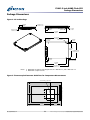
1
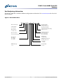
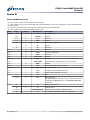
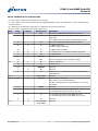
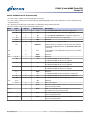
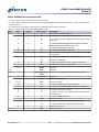
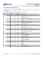
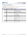
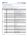
P300 2.5-Inch NAND Flash SSD
Features
P300 2.5-Inch SATA NAND Flash SSD
MTFDDACxxxSAL1x1
Features
•
•
•
•
•
•
•
•
•
•
•
• Reliability
– MTBF: 2 million hours
– 3-year warranty
– Static and dynamic wear leveling
– Field-upgradable firmware
– Uncorrectable bit error rate (UBER): <1 sector
per 1016 bits read
– Low power consumption: <7W (AVG)
• Endurance: Total bytes written (TBW) – 50GB
( 0.875PB); 100GB (1.75PB); 200GB (3.5PB)
• Mechanical/electrical
– Standard SATA connector
– 5V power (±10%)
– Dimensions: 100.45mm x 69.85mm x 9.5mm
– Weight: 100g
• Operating temperature: 0°C to 70°C
• Humidity (operating): 5% to 95% RH
• Shock and vibration
– 1500G/0.5ms
– 5–500Hz at 3.1G
• Capacity5: 50GB, 100GB, 200GB
Micron® SLC NAND Flash
RoHS-compliant package
SATA 6 Gb/s interface
ATA modes supported
– PIO modes 3 and 4
– Multiword DMA modes 0, 1, 2
– Ultra DMA modes 0, 1, 2, 3, 4, 5, 6
Industry-standard, 512-byte sector size support
Hot-plug capable
Native command queueing support with 32 command slot support
ATA8-ACS2 command set support
Secure erase (data page) command set
Self-monitoring, analysis, and reporting technology
(SMART) command set
Performance (empty/steady state)1, 2, 3, 4
– Sequential READ: up to 360/360 MB/s
– Sequential WRITE: up to 275/255 MB/s
– Random READ: up to 60,000/44,000 IOPs
– Random WRITE: up to 45,200/16,000 IOPs
– READ latency: 0.153/0.154ms (TYP)
– WRITE latency: 0.118/0.424ms (TYP)
Notes:
1. 128K transfers used for sequential READ/
WRITE values.
2. 4K transfers used for random READ/WRITE
latency values.
3. I/O performance numbers as measured using Iometer with a queue depth of 32 and
write cache disabled.
4. Performance values apply to all drive capacities.
5. 1GB = 1 billion bytes; formatted capacity is
less.
Warranty: Contact your Micron sales representative
for further information regarding the product,
including product warranties.
PDF: 09005aef840793dc
p300_2_5.pdf - Rev. K 5/12 EN
1
Micron Technology, Inc. reserves the right to change products or specifications without notice.
© 2010 Micron Technology, Inc. All rights reserved.
Products and specifications discussed herein are subject to change by Micron without notice.
P300 2.5-Inch NAND Flash SSD
Features
Part Numbering Information
The Micron® P300 SSD is available in different configurations and densities. Visit www.micron.com for a list of valid part numbers.
Figure 1: Part Number Chart
MT FD
D
AC xxx
S
AL - 1 N
Micron Technology
1 xx
ES
Production Status
Blank = Production
ES = Engineering sample
MS = Mechanical sample
Product Family
FD = Flash drive
Operating Temperature Range
Drive Interface
Blank = 0°C to 70°C
Drive Form Factor
AA = Contact factory
AB = Contact factory
AC = Contact factory
D = SATA 6.0 Gb/s
Hardware Feature Set
AC = 2.5-inch (9.5mm high)
BOM Revision
Drive Density
1 = 1st generation
050 = 50GB
100 = 100GB
200 = 200GB
NAND Flash Component
N = M62B, 16Gb, SLC, x8
Sector Size
1 = 512-byte
NAND Flash Type
Product Family
AL = P300
S = SLC
PDF: 09005aef840793dc
p300_2_5.pdf - Rev. K 5/12 EN
2
Micron Technology, Inc. reserves the right to change products or specifications without notice.
© 2010 Micron Technology, Inc. All rights reserved.
P300 2.5-Inch NAND Flash SSD
General Description
General Description
The Micron® P300 solid state drive (SSD) uses a single-chip controller with a SATA interface on the system side and n-channels of Micron NAND Flash internally. Packaged in
an industry standard 2.5-inch drive enclosure, the SSD integrates easily in existing storage infrastructures.
The Micron® P300 SSD is targeted at applications that require a high percentage of random READ/WRITE operations; high performance in terms of IOPs or latency, high endurance, high data retention; or applications that are deployed in harsh environments.
Figure 2: Functional Block Diagram
NAND
SATA
SSD
controller
NAND
NAND
NAND
NAND
DRAM
buffer
PDF: 09005aef840793dc
p300_2_5.pdf - Rev. K 5/12 EN
3
Micron Technology, Inc. reserves the right to change products or specifications without notice.
© 2010 Micron Technology, Inc. All rights reserved.
P300 2.5-Inch NAND Flash SSD
Architecture
Architecture
The P300 SSD is a NAND Flash storage device. A SATA 6 Gb/s interface connects to the
SSD externally and communicates with the controller. The controller manages data
transfers to and from the NAND Flash array.
Table 1: P300 Configurations
Unformatted Disk Density
NAND Flash Process NAND Flash Density Package Count Die per BGA Package
50GB
34nm
16Gb
16
2
100GB
34nm
16Gb
16
4
200GB
34nm
16Gb
16
8
1. Density is shown as user capacity (unformatted).
Note:
Logical Block Address Configuration
The drive is set to report the number of logical block addresses (LBA) that will ensure
sufficient storage space for the specified density. Standard LBA settings, based on the
IDEMA standard (LBA1-02), are shown below.
Table 2: Standard LBA Settings
Total LBAs
Drive
Size1
Decimal
Hexadecimal
50GB
97,696,368
100GB
195,371,568
200GB
390,721,968
Note:
Max LBA
User Available Bytes
Decimal
Hexadecimal
(Unformatted)
5D2BA70
97,696,367
5D2BA6F
50,020,549,632
BA52230
195,371,567
BA5222F
100,030,242,816
1749F1B0
390,721,967
1749F1AF
200,049,647,616
1. 1GB = 1,000,000,000 bytes.
Table 3: 2.5-Inch Nominal Dimensions and Weight
Value
Unit
Height
9.5
mm
Width
69.85
mm
Length
100.50
mm
<100
g
Unit weight
PDF: 09005aef840793dc
p300_2_5.pdf - Rev. K 5/12 EN
4
Micron Technology, Inc. reserves the right to change products or specifications without notice.
© 2010 Micron Technology, Inc. All rights reserved.
P300 2.5-Inch NAND Flash SSD
Architecture
Interface Connectors
The SATA signal segment interface cable has four conductors and three ground connections. As shown in Package Dimensions, the cable includes a 7-pin signal segment and a
9-pin power segment arranged in a single row with a 1.27mm (0.050in) pitch.
Table 4: SATA Signal Segment Pin Assignments
Signal Name
Type
Description
S1
GND
Ground
S2
A
S3
A#
S4
GND
S5
B#
S6
B
S7
GND
Differential signal pair A and A#
Ground
Differential signal pair B and B#
Ground
Table 5: 2.5-Inch SATA Power Segment Pin Assignments
Pin#
Signal Name
P1
V33
Description
No connect
P2
V33
No connect
P3
V33
No connect
P4
GND
Ground
P5
GND
Grond
P6
GND
Ground
P7
V5
5V power, precharge
P8
V5
5V power
P9
V5
5V power
P10
GND
Ground
P11
DAS1
Device activity signal
P12
GND
Ground
P13
V12
No connect
P14
V12
No connect
P15
V12
No connect
Note:
PDF: 09005aef840793dc
p300_2_5.pdf - Rev. K 5/12 EN
1. Pin 11 (DAS) may be optionally connected to GND.
5
Micron Technology, Inc. reserves the right to change products or specifications without notice.
© 2010 Micron Technology, Inc. All rights reserved.
P300 2.5-Inch NAND Flash SSD
Architecture
Figure 3: SSD Interface Connections
P1
S1
Power
segment
PDF: 09005aef840793dc
p300_2_5.pdf - Rev. K 5/12 EN
Signal
segment
6
Micron Technology, Inc. reserves the right to change products or specifications without notice.
© 2010 Micron Technology, Inc. All rights reserved.
P300 2.5-Inch NAND Flash SSD
Device ID
Device ID
Table 6: IDENTIFY Device ID
• F = The content of the word is fixed and does not change
• V = The content of the word is variable and may change depending on the state of the device or the commands executed by the device
• X = The fixed or variable type of this field is not defined in the governing standard
• R = The content of the word is reserved and shall be zero
Word
Bit(s)
Setting
Default Value
Description
00
15
F
0b
14–8
X
1000100b
0 = ATA device
Retired
7–6
F
01b
Obsolete
5–3
X
000b
Retired
2
V
0b
Response incomplete
1
X
0b
Retired
0b
Reserved
01
X
3FFFh
Obsolete
02
V
C837h
Specific configuration
03
X
0010h
Obsolete
04
X
0000h 0000h
06
X
003Fh
0
07
0000h 0000h
09
X
Retired
Obsolete
Reserved for the CompactFlash® Association (CFA)
0000h
Retired
Serial number (20 ASCII characters)
10
F
Varies
20
X
0000h 0000h 0000h
23
F
Varies
Firmware revision (8 ASCII characters)
27
F
Varies
Model number (40 ASCII characters)
15–8
F
80h
80h
7–0
F
10h
00h = Reserved
01h-FFh = Maximum number of logical sectors that shall be
transferred per DRQ data block on READ/WRITE MULTIPLE
commands
15
F
0b
Shall be cleared to 0
14
F
1b
Shall be set to 1
47
48
13–1
0
PDF: 09005aef840793dc
p300_2_5.pdf - Rev. K 5/12 EN
0000000000000b
F
0b
Retired/Obsolete
Reserved for the trusted computing group
1 = Trusted computing feature set is supported
7
Micron Technology, Inc. reserves the right to change products or specifications without notice.
© 2010 Micron Technology, Inc. All rights reserved.
P300 2.5-Inch NAND Flash SSD
Device ID
Table 6: IDENTIFY Device ID (Continued)
• F = The content of the word is fixed and does not change
• V = The content of the word is variable and may change depending on the state of the device or the commands executed by the device
• X = The fixed or variable type of this field is not defined in the governing standard
• R = The content of the word is reserved and shall be zero
Word
Bit(s)
Setting
Default Value
Description
49
15–14
13
F
12
1 = Standby timer values as specified in ATA-8 ACS-2 are
supported
0 = Standby timer values shall be managed by the device
0b
Reserved for IDENTIFY PACKET DEVICE command
F
1b
1 = IORDY supported
0 = IORDY may be supported
10
F
1b
1 = IORDY may be disabled
9
F
1b
1 = Shall be set to 1 to indicate that LBA is supported
8
F
1b
1 = DMA support
7–2
X
00000000b
Reserved
00b
Current long physical sector alignment setting
15
F
0b
Shall be cleared to 0
14
F
1b
Shall be set to 1
13–2
00000000b
Reserved
1
X
0b
Obsolete
0
F
1b
Shall be set to 1 to indicate vendor-specific standby timer
value minimum
X
0000h 0000h
F
00000000b
51
53
Reserved for IDENTIFY PACKET DEVICE command
1b
11
1–0
50
00b
15–8
7–3
00000b
Obsolete
Free-fall control sensitivity
00h = Vendor's recommended setting
01h-FFh = Sensitivity level; a larger number is a more sensitive setting
Reserved
2
F
1b
1 = The fields reported in word 88 are valid
0 = The fields reported in word 88 are not valid
1
F
1b
1 = The fields reported in words (70:64) are valid
0 = The fields reported in words (70:64) are not valid
0
X
1b
Obsolete
X
3FFh 0010h 003Fh
FC10h 00FBh
Obsolete
54
PDF: 09005aef840793dc
p300_2_5.pdf - Rev. K 5/12 EN
8
Micron Technology, Inc. reserves the right to change products or specifications without notice.
© 2010 Micron Technology, Inc. All rights reserved.
P300 2.5-Inch NAND Flash SSD
Device ID
Table 6: IDENTIFY Device ID (Continued)
• F = The content of the word is fixed and does not change
• V = The content of the word is variable and may change depending on the state of the device or the commands executed by the device
• X = The fixed or variable type of this field is not defined in the governing standard
• R = The content of the word is reserved and shall be zero
Word
Bit(s)
Setting
Default Value
Description
59
15
F
1b
1 = The BLOCK ERASE EXT command is supported
14
F
0b
1 = The OVERWRITE EXT command is supported
13
F
0b
1 = The CRYPTO SCRAMBLE EXT command is supported
12
F
1b
1 = The sanitize feature set is supported
11–9
1b
7–0
V
00000001b
Current setting for number of logical sectors that shall be
transferred per DRQ data block on READ/WRITE MULTIPLE
commands
F
Sect
Total number of user addressable logical sectors for 28-bit
commands
62
X
15–11
1 = Multiple sector setting is valid
0000h
Obsolete
00000b
Reserved
10
V
0b
1 = Multiword DMA mode 2 is selected
0 = Multiword DMA mode 2 is not selected
9
V
0b
1 = Multiword DMA mode 1 is selected
0 = Multiword DMA mode 1 is not selected
8
V
0b
1 = Multiword DMA mode 0 is selected
0 = Multiword DMA mode 0 is not selected
7–3
64
Reserved
V
60
63
000b
8
0000b
Reserved
2
F
1b
1 = Multiword DMA mode 2 and below is supported
1
F
1b
1 = Multiword DMA mode 1 and below is supported
0
F
1b
1 = Multiword DMA mode 0 is supported
00
Reserved
15–8
7–0
F
03h
65
F
0078h
Minimum multiword DMA transfer cycle time per word in
nanoseconds (cycle time)
66
F
0078h
MFR's recommended multiword DMA transfer cycle time
per word in nanoseconds (cycle time)
67
F
0078h
Minimum PIO transfer cycle time without flow control in
nanoseconds (cycle time)
F
0078h
Minimum PIO transfer cycle time with IORDY flow control in
nanoseconds (cycle time)
68
15–0
PDF: 09005aef840793dc
p300_2_5.pdf - Rev. K 5/12 EN
PIO modes support
9
Micron Technology, Inc. reserves the right to change products or specifications without notice.
© 2010 Micron Technology, Inc. All rights reserved.
P300 2.5-Inch NAND Flash SSD
Device ID
Table 6: IDENTIFY Device ID (Continued)
• F = The content of the word is fixed and does not change
• V = The content of the word is variable and may change depending on the state of the device or the commands executed by the device
• X = The fixed or variable type of this field is not defined in the governing standard
• R = The content of the word is reserved and shall be zero
Word
Bit(s)
Setting
Default Value
Description
69
15
F
0b
1 = CFast™ specification support
14
F
0b
1 = Deterministic read after trim is supported
13
F
0b
1 = Long physical sector alignment error reporting control is
supported
12
F
0b
1 = DEVICE CONFIGURATION IDENTIFY DMA and DEVICE
CONFIGURATION SET DMA are supported
11
F
0b
1 = READ BUFFER DMA is supported
10
F
0b
1 = WRITE BUFFER DMA is supported
9
F
0b
1 = SET MAX PASSWORD DMA and SET MAX UNLOCK DMA
are supported
8
F
0b
1 = DOWNLOAD MICROCODE DMA is supported
7
F
0b
Reserved for IEEE-1667
6
F
0b
1 = Optional ATA device 28-bit commands supported
5
F
0b
1 = Read zero after trim is supported
4–0
00000b
Reserved
70
0000h
Reserved
71
0000h 0000h 0000h
0000h
75
15–5
4–0
76
00000000000b
F
15–13
11111b
000b
Reserved for the IDENTIFY PACKET DEVICE command
Reserved
Maximum queue depth - 1
Reserved for SATA
12
F
1b
1 = Supports NCQueue priority information
11
F
0b
1 - Supports unload while NCQ commands outstanding
10
F
1b
1 = Supports PHY event counters
9
F
1b
1 = Supports receipt of host-initiated partial interface power management
8
F
1b
1 = Supports NCQ feature set
7–3
0000b
Reserved for SATA
2
F
1b
1 = Supports SATA Gen-2 signaling speed (3.0 Gb/s)
1
F
1b
1 = Supports SATA Gen-1 signaling speed (1.5 Gb/s)
0
F
0b
Shall be cleared to 0
V
0004h
77
PDF: 09005aef840793dc
p300_2_5.pdf - Rev. K 5/12 EN
Reserved for SATA
10
Micron Technology, Inc. reserves the right to change products or specifications without notice.
© 2010 Micron Technology, Inc. All rights reserved.
P300 2.5-Inch NAND Flash SSD
Device ID
Table 6: IDENTIFY Device ID (Continued)
• F = The content of the word is fixed and does not change
• V = The content of the word is variable and may change depending on the state of the device or the commands executed by the device
• X = The fixed or variable type of this field is not defined in the governing standard
• R = The content of the word is reserved and shall be zero
Word
Bit(s)
Setting
Default Value
Description
78
15–7
6
000000000b
F
5
79
1 = Supports software settings preservation
0b
Reserved for SATA
4
F
0b
1 = Supports in-order data delivery
3
F
1b
1 = Device supports initiating interface power management
(DIPM)
2
F
1b
1 = Supports DMA setup auto activation
1
F
0b
1 = Supports nonzero buffer offsets
0
F
0b
Shall be cleared to 0
15–7
6
000000000b
V
5
80
Reserved for SATA
1b
Reserved for SATA
1b
1 = Software settings preservation enabled
0b
Reserved for SATA
4
V
0b
1 = In-order data delivery enabled
3
V
0b
1 = Device initiated power management enabled
2
V
0b
1 = DMA setup auto-activation enabled
1
V
0b
1 = Nonzero buffer offsets enabled
0
F
0b
Shall be cleared to 0
15–10
000000b
Reserved
9
F
1b
1 = Supports ATA8-ACS2
8
F
1b
1 = Supports ATA-8-ACS
7
F
1b
1 = Supports ATA/ATAPI-7
6
F
1b
1 = Supports ATA/ATAPI-6
5
F
1b
1 = Supports ATA/ATAPI-5
4
F
1b
1 = Supports ATA/ATAPI-4
3
X
0b
Obsolete
2
X
0b
Obsolete
1
X
0b
Obsolete
0b
Reserved
0
81
Minor version number
F
PDF: 09005aef840793dc
p300_2_5.pdf - Rev. K 5/12 EN
0028h
0028h = ATA8-ACS version 6
11
Micron Technology, Inc. reserves the right to change products or specifications without notice.
© 2010 Micron Technology, Inc. All rights reserved.
P300 2.5-Inch NAND Flash SSD
Device ID
Table 6: IDENTIFY Device ID (Continued)
• F = The content of the word is fixed and does not change
• V = The content of the word is variable and may change depending on the state of the device or the commands executed by the device
• X = The fixed or variable type of this field is not defined in the governing standard
• R = The content of the word is reserved and shall be zero
Word
Bit(s)
Setting
Default Value
Description
82
15
X
0b
Obsolete
14
F
1b
1 = NOP command support
13
F
1b
1 = READ BUFFER command support
12
F
1b
1 = WRITE BUFFER command support
11
X
0b
Obsolete
10
F
1b
1 = Host-protected area feature set support
9
F
0b
Shall be cleared to 0 to indicate that the DEVICE RESET command is not supported
8
F
0b
1 = Service interrupt support
7
F
0b
1 = Release interrupt support
6
F
1b
1 = READ look-ahead support
5
F
1b
1 = Volatile write cache support
4
F
0b
Shall be cleared to 0 to indicate that the PACKET feature set
is not supported
3
F
1b
Shall be set to 1 to indicate that mandatory power management feature set is supported
2
X
0b
Obsolete
1
F
1b
1 = Security feature set support
0
F
1b
1 = SMART feature set support
PDF: 09005aef840793dc
p300_2_5.pdf - Rev. K 5/12 EN
12
Micron Technology, Inc. reserves the right to change products or specifications without notice.
© 2010 Micron Technology, Inc. All rights reserved.
P300 2.5-Inch NAND Flash SSD
Device ID
Table 6: IDENTIFY Device ID (Continued)
• F = The content of the word is fixed and does not change
• V = The content of the word is variable and may change depending on the state of the device or the commands executed by the device
• X = The fixed or variable type of this field is not defined in the governing standard
• R = The content of the word is reserved and shall be zero
Word
Bit(s)
Setting
Default Value
Description
83
15
F
0b
Shall be cleared to 0
14
F
1b
Shall be set to 1
13
F
1b
1 = FLUSH CACHE EXT command support
12
F
1b
Shall be set to 1 to indicate that the mandatory FLUSH
CACHE command is supported
11
F
1b
1 = Device configuration overlay feature set support
10
F
1b
1 = 48-bit address feature set support
9
F
0b
1 = Automatic acoustic management feature set support
8
F
1b
1 = SET MAX security extension support
7
84
0b
Reserved for address offset reserved area boot method
6
F
0b
1 = SET FEATURES subcommand required to spin up after
power up
5
F
0b
1 = Power-up in standby feature set support
4
X
0b
Obsolete
3
F
1b
1 = Advanced power management feature set support
2
F
0b
1 = CFA feature set support
1
X
0b
Obsolete
0
F
1b
1 = DOWNLOAD MICROCODE command support
15
F
0b
Shall be cleared to 0
14
F
1b
Shall be set to 1
13
F
1b
1 = The IDLE IMMEDIATE command with unload feature is
supported
0b
Reserved for TLC
12
0b
Reserved for TLC
10–9
11
X
00b
Obsolete
8
F
1b
1 = 64-bit worldwide name support
7
X
0b
Obsolete
6
F
1b
1 = WRITE DMA FUA EXT (and) WRITE MULTIPLE FUA EXT
commands are supported
5
F
1b
1 = General purpose logging feature set support
4
F
0b
1 = Streaming feature set support
3
F
0b
1 = Media card passthrough command feature set support
2
F
0b
1 = Media serial number support
1
F
1b
1 = SMART self-test support
0
F
1b
1 = SMART error logging support
PDF: 09005aef840793dc
p300_2_5.pdf - Rev. K 5/12 EN
13
Micron Technology, Inc. reserves the right to change products or specifications without notice.
© 2010 Micron Technology, Inc. All rights reserved.
P300 2.5-Inch NAND Flash SSD
Device ID
Table 6: IDENTIFY Device ID (Continued)
• F = The content of the word is fixed and does not change
• V = The content of the word is variable and may change depending on the state of the device or the commands executed by the device
• X = The fixed or variable type of this field is not defined in the governing standard
• R = The content of the word is reserved and shall be zero
Word
Bit(s)
Setting
Default Value
Description
85
86
15
X
0b
Obsolete
14
F
1b
1 = NOP command support
13
F
1b
1 = READ BUFFER command support
12
F
1b
1 = WRITE BUFFER command support
11
X
0b
Obsolete
10
V
1b
1 = Host-protected area feature set support
9
F
0b
1 = DEVICE RESET command support
8
V
0b
1 = Service interrupt enabled
7
V
0b
1 = Release interrupt enabled
6
V
1b
1 = Read look-ahead enabled
5
V
1b
1 = Volatile write cache enabled
4
F
0b
0 = Packet feature set is not supported
3
F
1b
1 = Power management feature set is enabled
2
X
0b
Obsolete
1
V
0b
1 = Security feature set enabled
0
V
1b
1 = SMART feature set enabled
15
F
1b
1 = Words 120 and 119 are valid
0b
1 = Reserved
14
13
F
1b
1 = FLUSH CACHE EXT command supported
12
F
1b
1 = FLUSH CACHE command supported
11
F
1b
1 = Device configuration overlay (DCO) feature set supported
10
F
1b
1 = 48-bit address feature set support
9
V
0b
1 = Automatic acoustic management feature set enabled
8
F
0b
1 = SET MAX security extension enabled by SET MAX SET
PASSWORD
7
0b
Reserved for address offset reserved area boot method
6
F
0b
1 = SET FEATURES subcommand required to spin up after
power up
5
V
0b
1 = Power-up in standby feature set enabled
4
X
0b
Obsolete
3
V
1b
1 = Advanced power management feature set enabled
2
F
0b
1 = CFA feature set enabled
1
X
0b
Obsolete
0
F
1b
1 = DOWNLOAD MICROCODE command support
PDF: 09005aef840793dc
p300_2_5.pdf - Rev. K 5/12 EN
14
Micron Technology, Inc. reserves the right to change products or specifications without notice.
© 2010 Micron Technology, Inc. All rights reserved.
P300 2.5-Inch NAND Flash SSD
Device ID
Table 6: IDENTIFY Device ID (Continued)
• F = The content of the word is fixed and does not change
• V = The content of the word is variable and may change depending on the state of the device or the commands executed by the device
• X = The fixed or variable type of this field is not defined in the governing standard
• R = The content of the word is reserved and shall be zero
Word
Bit(s)
Setting
Default Value
Description
87
15
F
0b
Shall be cleared to 0
14
F
1b
Shall be set to 1
13
F
1b
1 = IDLE IMMEDIATE command with unload feature support
0b
Reserved for TLC
12
0b
Reserved for TLC
10–9
11
X
00b
Obsolete
8
F
1b
1 = 64-bit worldwide name support
7
X
0b
Obsolete
6
F
1b
1 = WRITE DMA FUA EXT (and) WRITE MULTIPLE FUA EXT
commands are supported
5
F
1b
1 = General purpose logging feature set support
4
X
0b
Obsolete
3
V
0b
1 = Media card passthrough command feature set support
2
V
0b
1 = Media serial number is valid
1
F
1b
1 = SMART self-test support
0
F
1b
1 = SMART error logging support
PDF: 09005aef840793dc
p300_2_5.pdf - Rev. K 5/12 EN
15
Micron Technology, Inc. reserves the right to change products or specifications without notice.
© 2010 Micron Technology, Inc. All rights reserved.
P300 2.5-Inch NAND Flash SSD
Device ID
Table 6: IDENTIFY Device ID (Continued)
• F = The content of the word is fixed and does not change
• V = The content of the word is variable and may change depending on the state of the device or the commands executed by the device
• X = The fixed or variable type of this field is not defined in the governing standard
• R = The content of the word is reserved and shall be zero
Word
Bit(s)
Setting
Default Value
Description
88
15
0b
Reserved
14
V
0b
1 = Ultra DMA mode 6 is selected
0 = Ultra DMA mode 6 is not selected
13
V
0b
1 = Ultra DMA mode 5 is selected
0 = Ultra DMA mode 5 is not selected
12
V
0b
1 = Ultra DMA mode 4 is selected
0 = Ultra DMA mode 4 is not selected
11
V
0b
1 = Ultra DMA mode 3 is selected
0 = Ultra DMA mode 3 is not selected
10
V
0b
1 = Ultra DMA mode 2 is selected
0 = Ultra DMA mode 2 is not selected
9
V
0b
1 = Ultra DMA mode 1 is selected
0 = Ultra DMA mode 1 is not selected
8
V
0b
1 = Ultra DMA mode 0 is selected
0 = Ultra DMA mode 0 is not selected
7
89
0b
Reserved
6
F
1b
1 = Ultra DMA mode 6 and below supported
5
F
1b
1 = Ultra DMA mode 5 and below supported
4
F
1b
1 = Ultra DMA mode 4 and below supported
3
F
1b
1 = Ultra DMA mode 3 and below supported
2
F
1b
1 = Ultra DMA mode 2 and below supported
1
F
1b
1 = Ultra DMA mode 1 and below supported
0
F
1b
1 = Ultra DMA mode 0 support
00h
Reserved
01h
Time required for normal erase mode SECURITY ERASE UNIT
command
00h
Reserved
01h
Time required for enhanced erase mode SECURITY ERASE
UNIT command
15–8
7–0
90
F
15–8
7–0
F
91
V
00FEh
Current advanced power management value
92
V
0000h
Master password identifier
PDF: 09005aef840793dc
p300_2_5.pdf - Rev. K 5/12 EN
16
Micron Technology, Inc. reserves the right to change products or specifications without notice.
© 2010 Micron Technology, Inc. All rights reserved.
P300 2.5-Inch NAND Flash SSD
Device ID
Table 6: IDENTIFY Device ID (Continued)
• F = The content of the word is fixed and does not change
• V = The content of the word is variable and may change depending on the state of the device or the commands executed by the device
• X = The fixed or variable type of this field is not defined in the governing standard
• R = The content of the word is reserved and shall be zero
Word
Bit(s)
Setting
Default Value
Description
93
15
F
0b
Shall be cleared to 0
14
F
0b
Shall be set to 1
13
V
0b
1 = Device detected CBLID above ViH
0 = Device detected CBLID below ViL
0b
Reserved
12
11
V
0b
0 = Device 1 did not assert PDIAG
1 = Device asserted PDIAG
10–9
V
00b
These bits indicate how device 1 determined the device
number:
00 = Reserved
01 = Jumper used
10 = CSEL signal used
11 = Other method used or method used unknown
0b
Shall be set to 1
8
7
F
0b
Reserved
6
F
0b
0 = Device 0 does not respond when device 1 is selected
1 = Device 0 responds when device 1 is selected
5
V
0b
0 = Device 0 did not detect the assertion of DASP
1 = Device 0 detected the assertion of DASP
4
V
0b
0 = Device 0 does not detect the assertion of PDIAG
1 = Device 0 detected the assertion of PDIAG
3
V
0b
0 = Device 0 failed diagnostics
1 = Device 0 passed diagnostics
2–1
V
00b
These bits indicate how device 0 determined the device
number:
00 = Reserved
01 = Jumper used
10 = CSEL signal used
11 = Other method used or method used unknown
0
F
0b
Shall be set to 1
15–8
F
00h
Vendor's recommended auto acoustic management (AAM)
value
7–0
V
00h
Current auto acoustic management (AAM) value
95
F
0000h
Stream minimum request size
96
F
0000h
Streaming transfer time – DMA
97
F
0000h
Streaming access latency – DMA and PIO
98
F
0000h 0000h
94
PDF: 09005aef840793dc
p300_2_5.pdf - Rev. K 5/12 EN
Streaming performance granularity
17
Micron Technology, Inc. reserves the right to change products or specifications without notice.
© 2010 Micron Technology, Inc. All rights reserved.
P300 2.5-Inch NAND Flash SSD
Device ID
Table 6: IDENTIFY Device ID (Continued)
• F = The content of the word is fixed and does not change
• V = The content of the word is variable and may change depending on the state of the device or the commands executed by the device
• X = The fixed or variable type of this field is not defined in the governing standard
• R = The content of the word is reserved and shall be zero
Word
Bit(s)
Setting
Default Value
Description
100
F
LBA
104
F
0000h
Streaming transfer time – PIO
105
F
0008h
Maximum number of 512-byte blocks of LBA range entries
per DATA SET MANAGEMENT command
15
F
0b
Shall be cleared to 0
14
F
1b
Shall be set to 1
13
F
0b
1 = Device has multiple logical sectors per physical sector
12
F
0b
1 = Device logical sector size > 256 words
11–4
F
00000000b
3–0
F
0000b
2xP logical sectors per physical sector
F
0000h
Interseek delay for ISO-7779 standard acoustic testing
15–12
F
0101b
NAA (3–0)
11–0
F
000000001010b
IEEE OUI (23–12)
15–4
F
Varies
IEEE OUI (11–0)
Varies
Unique ID (35–32)
106
107
108
109
3–0
Maximum user LBA for 48-bit address feature set
Reserved
110
F
Varies
5–0 Unique ID (31–16)
111
F
Varies
Unique ID (15–0)
112
0000h 0000h 0000h
0000h
116
0000h
Reserved for TLC
F
0000h 0000h
Logical sector size
15
F
0b
Shall be cleared to 0
14
F
1b
Shall be set to 1
117
119
13–8
000000b
Reserved
Reserved
7
F
0b
1 = Extended power conditions feature set supported
6
F
1b
1 = Extended sense data reporting feature set supported
5
F
1b
1 = Free-fall control feature set supported
4
F
1b
1 = DOWNLOAD MICROCODE command with mode 3 supported
3
F
1b
1 = READ LOG DMA EXT (and) WRITE LOG DMA EXT command support
2
F
1b
1 = WRITE UNCORRECTABLE EXT support
1
F
0b
1 = Write-read-verify feature set support
0
F
0b
Reserved for DDT
PDF: 09005aef840793dc
p300_2_5.pdf - Rev. K 5/12 EN
18
Micron Technology, Inc. reserves the right to change products or specifications without notice.
© 2010 Micron Technology, Inc. All rights reserved.
P300 2.5-Inch NAND Flash SSD
Device ID
Table 6: IDENTIFY Device ID (Continued)
• F = The content of the word is fixed and does not change
• V = The content of the word is variable and may change depending on the state of the device or the commands executed by the device
• X = The fixed or variable type of this field is not defined in the governing standard
• R = The content of the word is reserved and shall be zero
Word
Bit(s)
Setting
Default Value
Description
120
15
F
0b
Shall be cleared to 0
14
F
1b
Shall be set to 1
13–8
000000b
7
V
0b
1 = At least one extended power conditions idle timer is enabled
6
V
0b
1 = Extended sense data reporting feature set enabled
5
V
0b
1 = Free-fall control feature set enabled
4
F
1b
1 = DOWNLOAD MICROCODE command with mode 3 supported
3
F
1b
1 = READ LOG DMA EXT (and) WRITE LOG DMA EXT command support
2
F
0b
1 = WRITE UNCORRECTABLE EXT support
1
V
0b
1 = Write-read-verify feature set enabled
0b
Reserved for DDT
0
121
0000h 0000h 0000h
0000h 0000h 0000h
127
128
X
15–9
8
V
7–6
Reserved for expanded support and enabled settings
0000h
Obsolete
0000000b
Reserved
0b
Master password capability: 0 = High, 1 = Maximum
00b
Reserved
5
F
1b
1 = Enhanced security erase support
4
V
0b
1 = Security count expired
3
V
0b
1 = Security frozen
2
V
0b
1 = Security locked
1
V
0b
1 = Security enabled
0
F
1b
1 = Security supported
X
Varies
F
0b
CFA power mode
129
160
Reserved
15
14
Vendor specific
0b
Word 160 supported
13
F
0b
CFA power mode 1 is required for one or more commands
implemented by the device
12
V
0b
CFA power mode 1 disabled
11–0
F
000000000000b
PDF: 09005aef840793dc
p300_2_5.pdf - Rev. K 5/12 EN
Maximum current in ma
19
Micron Technology, Inc. reserves the right to change products or specifications without notice.
© 2010 Micron Technology, Inc. All rights reserved.
P300 2.5-Inch NAND Flash SSD
Device ID
Table 6: IDENTIFY Device ID (Continued)
• F = The content of the word is fixed and does not change
• V = The content of the word is variable and may change depending on the state of the device or the commands executed by the device
• X = The fixed or variable type of this field is not defined in the governing standard
• R = The content of the word is reserved and shall be zero
Word
Bit(s)
Setting
Default Value
Description
161
168
169
F
15–4
000h
3–0
F
3h
15–1
F
000000000000000b
0
F
1b
F
0000h 0000h 0000h
0000h
170
174
0000h 0000h
176
206
0000h 0000h 0000h
0000h 0000h 0000h
0000h
F
15–12
X
11–6
Reserved for assignment by the CFA
Reserved
Device nominal form factor (DNFF)
Reserved
1 = Trim bit of the DATA SET MANAGEMENT command supported
Additional product identifier
Reserved
Varies
Current media serial number (60 ASCII characters; not supported)
0000b
Vendor specific
000000b
Reserved
5
F
1b
SCT data tables command support
4
F
1b
SCT FEATURES CONTROL command support
3
F
1b
SCT ERROR RECOVERY CONTROL command support
2
F
1b
SCT WRITE SAME command support
1
F
0b
Obsolete
0
F
1b
SCT command transport support
207
F
0000h 0000h
Reserved FOR CE-ATA
15
F
0b
Shall be cleared to 0
14
F
1b
Shall be set to 1
13–0
F
00000000000000b
210
V
0000h 0000h
Write-read-verify sector count mode 3
212
F
0000h 0001h
Write-read-verify sector count mode 2
15–12
F
0000b
NV cache feature set version
11–8
F
0000b
NV cache power mode feature set version
000b
Reserved
209
214
7–5
4
V
3–2
Logical sector offset within the first physical sector where
the first logical sector is placed
0b
1 = NV cache feature set enabled
00b
Reserved
1
V
0b
1 = NV cache power mode feature set enabled
0
F
0b
1 = NV cache power mode feature set support
PDF: 09005aef840793dc
p300_2_5.pdf - Rev. K 5/12 EN
20
Micron Technology, Inc. reserves the right to change products or specifications without notice.
© 2010 Micron Technology, Inc. All rights reserved.
P300 2.5-Inch NAND Flash SSD
Device ID
Table 6: IDENTIFY Device ID (Continued)
• F = The content of the word is fixed and does not change
• V = The content of the word is variable and may change depending on the state of the device or the commands executed by the device
• X = The fixed or variable type of this field is not defined in the governing standard
• R = The content of the word is reserved and shall be zero
Word
Bit(s)
Setting
Default Value
Description
215
V
0000h
NV cache size in logical blocks (LSW)
216
V
0000h
NV cache size in logical blocks (MSW)
217
F
0001h
Nominal media rotation rate
0000h
Reserved
00h
Reserved
00h
Device estimated time to spin up in seconds
00h
Reserved
00h
Write-read-verify feature set current mode
218
219
15–8
7–0
220
F
15–8
7–0
V
15–12
F
221
222
11–6
0000h
Reserved
0001b
Transport type: 0 = Parallel; 1 = SATA; 2–15 = Reserved
000000b
0 = Reserved
1 = Reserved
5
F
1b
0 = Reserved
1 = SATA Rev. 3.0
4
F
1b
0 = Reserved
1 = SATA Rev. 2.6
3
F
1b
0 = Reserved
1 = SATA Rev. 2.5
2
F
1b
0 = Reserved
1= SATA II: extensions
1
F
1b
0 = ATA/ATAPI-7
1= SATA 1.0a
0
F
1b
0 = ATA8-APT
1 = ATA8-AST
F
0000h
223
224
0000h 0000h 0000h
0000h 0000h 0000h
0000h 0000h 0000h
0000h
Transport minor revision number
Reserved
234
F
0001h
Minimum number of 512-byte units per DOWNLOAD MICROCODE command mode 3
235
F
00FFh
Maximum number of 512-byte units per DOWNLOAD MICROCODE command mode 3
PDF: 09005aef840793dc
p300_2_5.pdf - Rev. K 5/12 EN
21
Micron Technology, Inc. reserves the right to change products or specifications without notice.
© 2010 Micron Technology, Inc. All rights reserved.
P300 2.5-Inch NAND Flash SSD
Device ID
Table 6: IDENTIFY Device ID (Continued)
• F = The content of the word is fixed and does not change
• V = The content of the word is variable and may change depending on the state of the device or the commands executed by the device
• X = The fixed or variable type of this field is not defined in the governing standard
• R = The content of the word is reserved and shall be zero
Word
Bit(s)
Setting
Default Value
Description
236
255
0000h 0000h 0000h
0000h 0000h 0000h
0000h 0000h 0000h
0000h 0000h 0000h
0000h 0000h 0000h
0000h 0000h 0000h
0000h
Reserved
15–8
F
Varies
Checksum
7–0
F
A5h
Signature
PDF: 09005aef840793dc
p300_2_5.pdf - Rev. K 5/12 EN
22
Micron Technology, Inc. reserves the right to change products or specifications without notice.
© 2010 Micron Technology, Inc. All rights reserved.
P300 2.5-Inch NAND Flash SSD
Commands
Commands
Table 7: Supported ATA Command Set
See ATA8-ACS2 standard for command details
Command Name
PDF: 09005aef840793dc
p300_2_5.pdf - Rev. K 5/12 EN
Command Code (Hex)
CHECK POWER MODE
98h
CHECK POWER MODE
E5h
DEVICE CONFIGURATION
B1h
DOWNLOAD MICROCODE
92h
FLUSH CACHE
E7h
FLUSH CACHE EXT
EAh
IDLE
E3h
IDLE
97h
IDLE IMMEDIATE
95h
IDLE IMMEDIATE
E1h
NOP
00h
READ BUFFER
E4h
READ BUFFER DMA
E9h
READ DMA
C8h
READ DMA EXT
25h
READ DMA (without retries)
C9h
READ FPDMA QUEUED
60h
READ LOG DMA EXT
47h
READ LOG EXT
2Fh
READ MULTIPLE
C4h
READ MULTIPLE EXT
29h
READ NATIVE MAX ADDRESS
F8h
READ NATIVE MAX ADDRESS EXT
27h
READ SECTORS
20h
READ SECTORS EXT
24h
READ SECTORS (without retry)
21h
READ VERIFY SECTORS
40h
READ VERIFY SECTORS EXT
42h
READ VERIFY SECTORS (without retry)
41h
RECALIBRATE
10h
REQUEST SENSE DATA EXT
0Bh
SECURITY DISABLE PASSWORD
F6h
SECURITY ERASE PREPARE
F3h
SECURITY ERASE UNIT
F4h
SECURITY FREEZE LOCK
F5h
SECURITY SET PASSWORD
F1h
23
Micron Technology, Inc. reserves the right to change products or specifications without notice.
© 2010 Micron Technology, Inc. All rights reserved.
P300 2.5-Inch NAND Flash SSD
Commands
Table 7: Supported ATA Command Set (Continued)
See ATA8-ACS2 standard for command details
Command Name
PDF: 09005aef840793dc
p300_2_5.pdf - Rev. K 5/12 EN
Command Code (Hex)
SECURITY UNLOCK
F2h
SEEK
70h
SET FEATURES
EFh
SET MAX ADDRESS
F9h
SET MULTIPLE MODE
C6h
SET NATIVE MAX ADDRESS EXT
37h
SLEEP
99h
SLEEP
E6h
SMART
B0h
STANDBY
E2h
STANDBY
96h
STANDBY IMMEDIATE
94h
STANDBY IMMEDIATE
E0h
WRITE BUFFER
E8h
WRITE BUFFER DMA
EBh
WRITE DMA
CAh
WRITE DMA EXT
35h
WRITE DMA FUA EXT
3Dh
WRITE DMA (without retries)
CBh
WRITE FPDMA QUEUED
61h
WRITE LOG DMA EXT
57h
WRITE LOG EXT
3Fh
WRITE MULTIPLE
C5h
WRITE MULTIPLE EXT
39h
WRITE MULTIPLE FUA EXT
CEh
WRITE SECTORS
30h
WRITE SECTORS EXT
34h
WRITE SECTORS (without retry)
31h
24
Micron Technology, Inc. reserves the right to change products or specifications without notice.
© 2010 Micron Technology, Inc. All rights reserved.
P300 2.5-Inch NAND Flash SSD
Reliability
Reliability
Micron SSDs incorporate advanced technology for defect and error management. Micron uses various combinations of hardware-based error correction algorithms and
firmware-based static and dynamic wear-leveling algorithms.
Over the life of the SSD, uncorrectable errors may occur. An uncorrectable error is defined as data that is reported as successfully programmed to the SSD but when it is read
out of the SSD, the data differs from what was programmed.
Table 8: Uncorrectable Bit Error Rate
Uncorrectable Bit Error Rate
Operation
1016
READ
<1 sector per
bits read
Mean Time Between Failures
Mean time between failures (MTBFs) for the SSD can be predicted based on the component reliability data using the methods referenced in the Telcordia SR-332 reliability
prediction procedures for electronic equipment.
Table 9: MTBFs
MTBF (Operating Hours)1
Density
Note:
50GB
2 million
100GB
2 million
200GB
2 million
1. The product achieves a mean time between failure (MTBF) of 2 million hours, based on
population statistics not relevant to individual units.
Endurance
Endurance for the SSD can be predicted based on the usage conditons applied to the
device, the internal NAND component cycles, the write amplification factor, and the
wear-leveling efficency of the drive. The table below shows the drive lifetime for each
SSD density based on predefined usage conditions.
Table 10: Drive Lifetime
Density
Notes:
PDF: 09005aef840793dc
p300_2_5.pdf - Rev. K 5/12 EN
Drive Lifetime (Total Bytes Written)
50GB
.875PB
100GB
1.75PB
200GB
3.5PB
1. Total bytes written calculated with the drive 100% full.
2. Access patterns are 50% sequential and 50% random. Random accesses: 10% are 512B;
50% are 4K; 15% are 32K; 15% are 64K; and 10% are 128K. Sequential accesses: 100%
are 128K.
25
Micron Technology, Inc. reserves the right to change products or specifications without notice.
© 2010 Micron Technology, Inc. All rights reserved.
P300 2.5-Inch NAND Flash SSD
Reliability
Data Retention
Micron SSD data retention at beginning of life: 10 years at 25°C
Micron SSD data retention at end of life: 1 year at 25°C
PDF: 09005aef840793dc
p300_2_5.pdf - Rev. K 5/12 EN
26
Micron Technology, Inc. reserves the right to change products or specifications without notice.
© 2010 Micron Technology, Inc. All rights reserved.
P300 2.5-Inch NAND Flash SSD
Electrical Characteristics
Electrical Characteristics
Table 11: SATA Typical Power Consumption
Idle/Standby/Sleep
Secure Erase
SEQ
Write/Read
(128K XFR)
50GB
125
1000
2500/1800
1900/1500
mW
100B
125
1200
3000/2000
2200/1700
mW
200GB
125
1400
3500/2200
2500/1900
mW
Density
RND
Write/Read
(4K XFR)
Unit
Table 12: Maximum Ratings
Parameter/Condition
Symbol
Min
Max
Unit
Voltage input
V5
4.5
5.5
V
Operating temperature
TA
0
70
°C
–40
85
°C
Rate of temperature change
–
20
°C/hour
Relative humidity (noncondensing)
5
95
%
Non-operating temperature
Stresses greater than those listed may cause permanent damage to the device. This is a
stress rating only, and functional operation of the device at these or any other conditions above those indicated in the operational sections of this specification is not implied. Exposure to absolute maximum rating conditions for extended periods may affect
reliability.
Table 13: Shock and Vibration
Parameter/Condition
Specification
Operating shock
1500G/0.5ms
Operating vibration
PDF: 09005aef840793dc
p300_2_5.pdf - Rev. K 5/12 EN
5–500Hz at 3.1G
27
Micron Technology, Inc. reserves the right to change products or specifications without notice.
© 2010 Micron Technology, Inc. All rights reserved.
P300 2.5-Inch NAND Flash SSD
Compliance
Compliance
Micron SSDs comply with the following:
•
•
•
•
•
•
•
•
•
•
•
•
•
RoHS compliant
Halogen free
SATA-IO
WHQL
CE (Europe): EN55022, 2006 Class B and EN55024, 1998 + A1: 2001 + A2:2003
FCC: CFR Title 47, Part 15, ICES-003, all Class B
UL (US): approval to UL-60950-1, 2nd Edition, 2007-03-27, IEC 60950-1:2005, 2nd Edition
BSMI (Taiwan): approval to CNS 13438
C-TICK (Australia, New Zealand): approval to AS/NZS CISPR22
KCC RRL (Korea): approval to KCC MU2-C30025, KCC MU2-C30018 Class B
W.E.E.E.: Compliance with EU WEEE directive 2002/96/EC. Additional obligations
may apply to customers who place these products in the markets where WEEE is enforced.
TUV (Germany): approval to IEC60950/EN60950
VCCI
FCC Rules
This equipment has been tested and found to comply with the limits for a Class A digital
device, pursuant to part 15 of the FCC Rules. These limits are designed to provide reasonable protection against harmful interference when the equipment is operated in a
commercial environment. This equipment generates, uses, and can radiate radio frequency energy and, if not installed and used in accordance with the instruction manual,
may cause harmful interference to radio communications. Operation of this equipment
in a residential area is likely to cause harmful interference in which case the user will be
required to correct the interference at his own expense.
PDF: 09005aef840793dc
p300_2_5.pdf - Rev. K 5/12 EN
28
Micron Technology, Inc. reserves the right to change products or specifications without notice.
© 2010 Micron Technology, Inc. All rights reserved.
P300 2.5-Inch NAND Flash SSD
Package Dimensions
Package Dimensions
Figure 4: 2.5-Inch Package
13.43mm
0.529in
9.50mm ±0.20
0.374in ±0.008
14.00mm
0.551in
3.50mm ±0.38
0.138in ±0.015
M3 x 0.5mm
(2 PLCS)
3.00mm
0.118in
90.60mm
3.567in
(100.50mm)
(3.957in)
(0.30mm)
(0.012in)
M3 x 0.5mm
4.07mm
0.160in
61.71mm
2.430in
69.85mm ±0.25
2.750in ±0.010
9.40mm
0.370in
14.00mm
0.551in
3.0mm
0.12in RAD
90.60mm
3.567in
100.20mm ±0.25
3.945in ±0.01
Notes:
1. Maximum mounting screw length: Bottom = M3 x 0.5 x 3; Side = M3 x 0.5 x 4
2. Maximum torque: 4.5 in-lb
Figure 5: Thermocouple Placement Guidelines for Temperature Measurement
Center thermocouple here
35.5mm
Power and data connectors
Non-label side of SSD
3mm
3mm
3mm
3mm
34.5mm
71.2mm
PDF: 09005aef840793dc
p300_2_5.pdf - Rev. K 5/12 EN
30.8mm
29
Micron Technology, Inc. reserves the right to change products or specifications without notice.
© 2010 Micron Technology, Inc. All rights reserved.
P300 2.5-Inch NAND Flash SSD
References
References
• Serial ATA: High-speed serialized AT attachment, Serial ATA working group, available
at www.sata-io.org
• Small Form Factor Specification SFF-8201, SFF-8223
• Electronic Industries Association Standard, EIA-720
• Telcordia SR-332 reliability prediction procedures for electronic equipment
• IDEMA Document LBA1-02
PDF: 09005aef840793dc
p300_2_5.pdf - Rev. K 5/12 EN
30
Micron Technology, Inc. reserves the right to change products or specifications without notice.
© 2010 Micron Technology, Inc. All rights reserved.
P300 2.5-Inch NAND Flash SSD
Revision History
Revision History
Rev. K – 5/12
• Added center thermocouple graphic to package dimensions.
Rev. J – 4/12
• Added notes to package dimension graphic.
Rev. I – 10/11
• Added FCC rules to Compliance.
Rev. H – 5/11
• Added DOWNLOAD MICROCODE command to Table 7: Supported ATA Command
Set; changed hex format of command codes.
Rev. G – 5/11
• Changed overall length of the enclosure + connector from absolute maximums to reference dimensions in packaging figure.
Rev. F – 4/11
• Removed references to altitude from Features section.
Rev. E – 4/11
• Removed references to green from Compliance section.
8000 S. Federal Way, P.O. Box 6, Boise, ID 83707-0006, Tel: 208-368-3900
www.micron.com/productsupport Customer Comment Line: 800-932-4992
Micron and the Micron logo are trademarks of Micron Technology, Inc.
All other trademarks are the property of their respective owners.
This data sheet contains minimum and maximum limits specified over the power supply and temperature range set forth herein.
Although considered final, these specifications are subject to change, as further product development and data characterization sometimes occur.
PDF: 09005aef840793dc
p300_2_5.pdf - Rev. K 5/12 EN
31
Micron Technology, Inc. reserves the right to change products or specifications without notice.
© 2010 Micron Technology, Inc. All rights reserved.