1
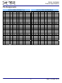
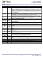
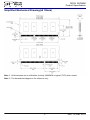
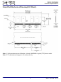
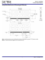
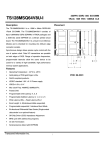
DDR3 SODIMM
Product Specification
Features
• DDR3 functionality and operations supported as defined in the component data sheet
• 204pin, small-outline dual in-line memory module (SODIMM)
• Fast data transfer rates: PC3-8500, PC3-10600,PC3-12800
• Single or Dual rank
• 1GB(128 Meg x 8), 2GB (256 Meg x 64), 4GB (512Meg x 64)
• V DD = V DDQ = 1.5V ±0.075V
• V DDSPD = 3.0V to 3.6V
• Reset pin for improved system stability
• Nominal and dynamic on-die termination (ODT) for data, strobe, and mask signals
• Fixed burst chop (BC) of 4 and burst length (BL) of 8 via the mode register set (MRS)
• Adjustable data-output drive strength
• Fly-by topology
• Terminated control, command, and address bus
• Serial presence-detect (SPD) EEPROM
• Gold edge contacts
• Pb-free
1
Rev. 1.4 Dec. 2011
DDR3 SODIMM
Product Specification
Module Specification
Part Number
SP001GBSTU106S01(2)
SP001GBSTU133S01(2)
SP001GBSTU106T01(2)
SP001GBSTU133T01(2)
SP001GBSTU106Q01(2)
SP001GBSTU133Q01(2)
SP002GBSTU106V01(2)
SP002GBSTU133V01(2)
SP002GBSTU160V01(2)
SP002GBSTU106S01(2)
SP002GBSTU133S01(2)
SP002GBSTU160S01(2)
SP002GBSTU106T01(2)
SP002GBSTU133T01(2)
SP004GBSTU106V01(2)
Module Density &
Configuration
1GB (128Mx64)
128Mx8 1Rank
1GB (128Mx64)
128Mx8 1Rank
1GB (128Mx64)
64Mx16 2Ranks
2GB (256Mx64)
256Mx8 1Rank
2GB (256Mx64)
128Mx8 2Ranks
2GB (256Mx64)
128Mx16 2Ranks
Bandwidth
Data Rate
Timing
(tCL-tRCD-tRP)
PC3-8500
DDR3-1066
7-7-7
PC3-10600
DDR3-1333
9-9-9
PC3-8500
DDR3-1066
7-7-7
PC3-10600
DDR3-1333
9-9-9
PC3-8500
DDR3-1066
7-7-7
PC3-10600
DDR3-1333
9-9-9
PC3-8500
DDR3-1066
7-7-7
PC3-10600
DDR3-1333
9-9-9
PC3-12800
DDR3-1600
11-11-11
PC3-8500
DDR3-1066
7-7-7
PC3-10600
DDR3-1333
9-9-9
PC3-12800
DDR3-1600
9-9-9
PC3-8500
DDR3-1066
7-7-7
PC3-10600
DDR3-1333
9-9-9
2GB (256Mx64)
128Mx8 2Ranks
PC3-8500
DDR3-1066
7-7-7
PC3-10600
DDR3-1333
9-9-9
PC3-12800
DDR3-1600
11-11-11
SP008GBSTU106V21(2)
4GB x 2 Kit Package
PC3-8500
DDR3-1066
7-7-7
SP008GBSTU133V21(2)
4GB x 2 Kit Package
PC3-10600
DDR3-1333
9-9-9
SP004GBSTU133V01(2)
SP004GBSTU160V01(2)
Note:
1. This document supports all STU Series DDR3 204Pin SODIMM products.
2. Some item was being EOL in this list, Please contact with our sales Dep.
3. All part numbers end with a double-digit code is for customize use only.
Example: SP001GBSTU133S02-XX
2
Rev. 1.4 Dec. 2011
DDR3 SODIMM
Product Specification
Pin Assignments
204-Pin DDR3 SODIMM Front
204-Pin DDR3 SODIMM Back
Pin
Symbol
Pin
Symbol
Pin
Symbol
Pin
Symbol
Pin
Symbol
Pin
Symbol
Pin
Symbol
Pin
1
VREFDQ
53
DQ19
105
VDD
157
DQ42
2
VSS
54
VSS
106
VDD
158
Symbol
DQ46
3
VSS
55
VSS
107
A10
159
DQ43
4
DQ4
56
DQ28
108
BA1
160
DQ47
5
DQ0
57
DQ24
109
BA0
161
VSS
6
DQ5
58
DQ29
110
RAS#
162
VSS
7
DQ1
59
DQ25
111
VDD
163
DQ48
8
VSS
60
VSS
112
VDD
164
DQ52
DQ53
9
VSS
61
VSS
113
WE#
165
DQ49
10
DQS0#
62
DQS3#
114
S0#
166
11
DM0
63
DM3
115
CAS#
167
VSS
12
DQS0
64
DQS3
116
ODT0
168
VSS
13
VSS
65
VSS
117
VDD
169
DQS6#
14
VSS
66
VSS
118
VDD
170
DM6
15
DQ2
67
DQ26
119
A13
171
DQS6
16
DQ6
68
DQ30
120
ODT1
172
VSS
17
DQ3
69
DQ27
121
S1#
173
VSS
18
DQ7
70
DQ31
122
NC
174
DQ54
19
VSS
71
VSS
123
VDD
175
DQ50
20
VSS
72
VSS
124
VDD
176
DQ55
21
DQ8
73
CKE0
125
NC
177
DQ51
22
DQ12
74
CKE1
126
VREFCA
178
VSS
23
DQ9
75
VDD
127
VSS
179
VSS
24
DQ13
76
VDD
128
SS
180
DQ60
25
VSS
77
NC
129
DQ32
181
DQ56
26
VSS
78
NC
130
DQ36
182
DQ61
27
DQS1#
79
BA2
131
DQ33
183
DQ57
28
DM1
80
NC/A14
132
DQ37
184
VSS
29
DQS1
81
VDD
133
VSS
185
VSS
30
RESET#
82
VDD
134
VSS
186
DQS7#
31
VSS
83
A12
135
DQS4#
187
DM7
32
VSS
84
A11
136
DM4
188
DQS7
33
DQ10
85
A9
137
DQS4
189
VSS
34
DQ14
86
A7
138
VSS
190
VSS
35
DQ11
87
VDD
139
VSS
191
DQ58
36
DQ15
88
VDD
140
DQ38
192
DQ62
37
VSS
89
A8
141
DQ34
193
DQ59
38
VSS
90
A6
142
DQ39
194
DQ63
39
DQ16
91
A5
143
DQ35
195
VSS
40
DQ20
92
A4
144
VSS
196
VSS
41
DQ17
93
VDD
145
VSS
197
SA0
42
DQ21
94
VDD
146
DQ44
198
EVENT#
43
VSS
95
A3
147
DQ40
199
VDDSPD
44
VSS
96
A2
148
DQ45
200
SDA
45
DQS2#
97
A1
149
DQ41
201
SA1
46
DM2
98
A0
150
VSS
202
SCL
47
DQS2
99
VDD
151
VSS
203
VTT
48
VSS
100
VDD
152
DQS5#
204
VTT
49
VSS
101
CK0
153
DM5
–
–
50
DQ22
102
CK1
154
DQS5
–
–
51
DQ18
103
CK0#
155
VSS
–
–
52
DQ23
104
CK1#
156
VSS
–
–
3
Rev. 1.4 Dec. 2011
DDR3 SODIMM
Product Specification
Pin Description
Symbol
Type
A0–A14
Input
BA0–BA2
Input
Description
Address inputs: Provide the row address for ACTIVE commands and the column address
and auto precharge bit for READ/WRITE commands to select one location out of the memory
array in the respective bank. A10 is sampled during a PRECHARGE command to determine
whether the PRECHARGE applies to one bank (A10 LOW) or all banks (A10 HIGH). If only
one bank is to be precharged, the bank is selected by BA. A12 is sampled during READ and
WRITE commands to determine if burst chop (on-the-fly) will be performed. The address
inputs also provide the opcode during mode register command set. A0–A13 (128Mx8)
A0–A14 (256Mx8).
Bank address inputs: BA0, BA1 define to which device bank an ACTIVE, READ, WRITE, or
PRECHARGE command is being applied. BA0, BA1 define which mode register, including
MR, EMR, EMR(2), and EMR(3), is loaded during the LOAD MODE command.
Clock: CK and CK# are differential clock inputs. All address and control input signals are
sampled on the crossing of the positive edge of CK and negative edge of CK#. Output data
(DQs and DQS/DQS#) is referenced to the crossings of CK and CK#.
Clock enable: CKE (registered HIGH) activates and CKE (registered LOW) deactivates
CKE0, CKE1
Input
clocking circuitry on the DDR3 SDRAM.
Data input mask: DM is an input mask signal for write data. Input data is masked when DM is
sampled HIGH, along with that input data, during a write access. DM is sampled on both
DM0–DM7
Input
edges of DQS. Although DM pins are input-only, the DM loading is designed to match that of
DQ and DQS7pins.
On-die termination: ODT (registered HIGH) enables termination resistance internal to the
ODT0
DDR3 SDRAM. When enabled, ODT is only applied to the following pins: DQ, DQS, DQS#
Input
ODT1
and DM. The ODT input will be ignored if disabled via the LOAD MODE command.
RAS#, CAS#,
Command inputs: RAS#, CAS#, and WE# (along with S#) define the command being
Input
WE#
entered.
Reset: RESET# is an active LOW CMOS input referenced to V SS . The RESET# input receiver
Input
RESET#
a CMOS input defined as a rail-to-rail signal with DC HIGH ≥ 0.8 ×V DD and DC LOW ≤ 0.2
(LVCMOS) is
×V DD .
Chip select: S# enables (registered LOW) and disables (registered HIGH) the command
S0#, S1#
Input
decoder.
Presence-detect address inputs: These pins are used to configure the SPD EEPROM
SA[2:0]
Input
address range.
Serial clock for presence-detect: SCL is used to synchronize the presence-detect data
SCL
Input
transfer to and from the module.
DQ0–DQ63
I/O
Data input/output: Bidirectional data bus.
DQS0–DQS7
Data
strobe: Output with read data, input with write data for source synchronous operation.
I/O
DQS0#–DQS7#
Edge-aligned with read data, center-aligned with write data.
Serial presence-detect data: SDA is a bidirectional pin used to transfer addresses and data
SDA
I/O
into and out of the SPD EEPROM on the module.
Power supply: 1.5V ±0.075V. The component V DD and V DDQ are connected to the module
V DD
Supply
V DD .
V DDSPD
Supply
Temperature sensor/SPD EEPROM power supply: +3.0V to +3.6V.
V REFCA
Supply
Reference voltage: Control, command, and address (V DD /2).
V REFDQ
Supply
Reference voltage: DQ, DM (V DD /2).
V SS
Supply
Ground.
V TT
Supply
Termination voltage: Used for control, command, and address (V DD /2).
NC
–
No connect: These pins are not connected on the module.
NU
–
Not used: These pins are not used in specific module configuration/operations.
CK0, CK0#,
CK1, CK1#
Input
4
Rev. 1.4 Dec. 2011
DDR3 SODIMM
Product Specification
Simplified Mechanical Drawing(x8 1Rank)
Note: 1. All dimensions are in millimeters (inches); MAX/MIN or typical (TYP) where noted.
Note: 2. The dimensional diagram is for reference only.
5
Rev. 1.4 Dec. 2011
DDR3 SODIMM
Product Specification
Simplified Mechanical Drawing(x16 1Rank)
Note: 1. All dimensions are in millimeters (inches); MAX/MIN or typical (TYP) where noted.
Note: 2. The dimensional diagram is for reference only.
6
Rev. 1.4 Dec. 2011
DDR3 SODIMM
Product Specification
Simplified Mechanical Drawing(x8 2Ranks)
Note 1: All dimensions are in millimeters (inches); MAX/MIN or typical (TYP) where noted.
Note 2: The dimensional diagram is for reference only.
7
Rev. 1.4 Dec. 2011
DDR3 SODIMM
Product Specification
Simplified Mechanical Drawing(x16 2Ranks)
Note 1: All dimensions are in millimeters (inches); MAX/MIN or typical (TYP) where noted.
Note 2: The dimensional diagram is for reference only.
8
Rev. 1.4 Dec. 2011