1
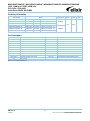
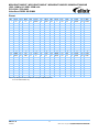
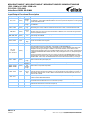
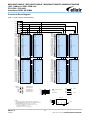
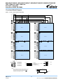
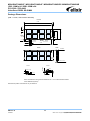
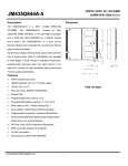
M2N1G64TUH8G5F / M2S1G64TUH8G4F / M2N2G64TU8HG5B / M2N2G64TU8HG4B 1GB: 128M x 64 / 2GB: 256M x 64 PC2-5300 / PC2-6400 Unbuffered DDR2 SO-DIMM Based on DDR2-667/800 64Mx16 (1GB)/128Mx8 (2GB) SDRAM G-Die Features • Performance: Speed Sort PC2-5300 PC2-6400 -3C -AC Unit DIMM CAS Latency 5 5 fck – Clock Freqency 333 400 MHz 3 2.5 ns 667 800 Mbps tck – Clock Cycle Data Transfer Speed • 200-Pin Small Outline Dual In-Line Memory Module (SO-DIMM) • 1GB: 128Mx64 Unbuffered DDR2 SO-DIMM based on 64M x16 DDR2 SDRAM G-Die devices. • 2GB: 256Mx64 Unbuffered DDR2 SO-DIMM based on 128M x8 DDR2 SDRAM G-Die devices. • Intended for 333MHz and 400MHz applications • Inputs and outputs are SSTL-18 compatible • VDD = VDDQ = 1.8V ±0.1V • SDRAMs have 8 internal banks for concurrent operation • Differential clock inputs • Data is read or written on both clock edges • DRAM DLL aligns DQ and DQS transitions with clock transitions. • Address and control signals are fully synchronous to positive clock edge • Auto Refresh (CBR) and Self Refresh Modes • Automatic and controlled precharge commands • Programmable Operation: - DIMM Latency: 3, 4, 5 - Burst Type: Sequential or Interleave - Burst Length: 4, 8 - Operation: Burst Read and Write • 13/10/2 Addressing (1GB) • 14/10/2 Addressing (2GB) • 7.8 s Max. Average Periodic Refresh Interval • Serial Presence Detect • Gold contacts • 1GB module’s SDRAMs are 84-ball BGA Package • 2GB module’s SDRAMs are 60-ball BGA Package • RoHS compliance Description M2N1G64TUH8G5F / M2S1G64TUH8G4F / M2N2G64TU8HG5B / M2N2G64TU8HG4B are unbuffered 200-Pin Double Data Rate 2 (DDR2) Synchronous DRAM Small Outline Dual In-Line Memory Module (SO-DIMM), organized as two ranks of 128Mx64 (1GB)/256Mx64 (2GB) high-speed memory array. M2N1G64TUH8G5F / M2S1G64TUH8G4F uses eight 64Mx16 84-ball BGA packaged devices and M2N2G64TU8HG5B / M2N2G64TU8HG4B uses sixteen 128Mx8 60-ball BGA packaged devices. These DIMMs are manufactured using raw cards developed for broad industry use as reference designs. The use of these common design files minimizes electrical variation between suppliers. All Elixir DDR2 SODIMMs provide a high-performance, flexible 8-byte interface in a space-saving footprint. The DIMM is intended for use in applications operating of 333MHz/400MHz clock speeds and achieves high-speed data transfer speed of 667Mbps/800Mbps. Prior to any access operation, the device latency and burst/length/operation type must be programmed into the DIMM by address inputs A0-A12 (1GB) / A0-A13 (2GB) and I/O inputs BA0, BA1 and BA2 using the mode register set cycle. The DIMM uses serial presence-detect implemented via a serial EEPROM using a standard IIC protocol. The first 128 bytes of SPD data are programmed and locked during module assembly. The remaining 128 bytes are available for use by the customer. REV 1.0 07/2010 1 © NANYA TECHNOLOGY CORPORATION NANYA reserves the right to change products and specifications without notice. M2N1G64TUH8G5F / M2S1G64TUH8G4F / M2N2G64TU8HG5B / M2N2G64TU8HG4B 1GB: 128M x 64 / 2GB: 256M x 64 PC2-5300 / PC2-6400 Unbuffered DDR2 SO-DIMM Ordering Information Part Number Speed Organization M2N2G64TU8HG5B-AC DDR2-800 PC2-6400 400MHz (2.5ns @ CL = 5) M2N2G64TU8HG5B-3C DDR2-667 PC2-5300 333MHz (3.0ns @ CL = 5) M2N2G64TU8HG4B-AC DDR2-800 PC2-6400 400MHz (2.5ns @ CL = 5) M2N1G64TUH8G5F-AC DDR2-800 PC2-6400 400MHz (2.5ns @ CL = 5) M2N1G64TUH8G5F-3C DDR2-667 PC2-5300 333MHz (3.0ns @ CL = 5) M2S1G64TUH8G4F-AC DDR2-800 PC2-6400 400MHz (2.5ns @ CL = 5) Power Leads 1.8V Gold Note 256Mx64 128Mx64 Pin Description CK0, CK1, , Differential Clock Inputs CKE0, CKE1 DQ0-DQ63 Data input/output Clock Enable DQS0-DQS7 Bidirectional data strobes - Differential data strobes Row Address Strobe Column Address Strobe Write Enable VDD Power (1.8V) , Chip Selects VREF Ref. Voltage for SSTL_18 inputs A0-A9 A11-A13 DM0-DM7 Row Address Inputs VDDSPD Input Data Masks Serial EEPROM positive power supply A0-A9 Column Address Inputs VSS Ground A10/AP Column Address Input/Auto-precharge SCL Serial Presence Detect Clock Input Serial Presence Detect Data input/output BA0, BA1, BA2 SDRAM Bank Address Inputs SDA ODT0, ODT1 Active termination control lines SA0, SA1 NC Serial Presence Detect Address Inputs No Connect Note: A13 is for 2GB modules only. REV 1.0 07/2010 2 © NANYA TECHNOLOGY CORPORATION NANYA reserves the right to change products and specifications without notice. M2N1G64TUH8G5F / M2S1G64TUH8G4F / M2N2G64TU8HG5B / M2N2G64TU8HG4B 1GB: 128M x 64 / 2GB: 256M x 64 PC2-5300 / PC2-6400 Unbuffered DDR2 SO-DIMM Pinout Pin Front Pin Back Pin Front Pin Back Pin Front Pin Back Pin Front Pin Back 1 VREF 3 VSS 2 VSS 51 DQS2 52 DM2 4 DQ4 53 VSS 54 VSS 101 A1 103 VDD 102 A0 151 DQ42 152 DQ46 104 VDD 153 DQ43 154 DQ47 5 DQ0 6 DQ5 55 DQ18 56 DQ22 105 A10/AP 106 BA1 155 VSS 156 VSS 7 DQ1 9 VSS 8 VSS 57 DQ19 10 DM0 59 VSS 58 DQ23 60 VSS 107 BA0 108 157 DQ48 158 DQ52 109 110 159 DQ49 160 DQ53 11 12 VSS 61 DQ24 62 DQ28 111 VDD 112 VDD 161 VSS 162 VSS 13 15 DQS0 14 DQ6 VSS 16 DQ7 63 DQ25 65 VSS 64 DQ29 113 114 ODT0 163 NC 164 CK1 66 VSS 115 116 A13/NC 165 VSS 166 17 DQ2 18 19 DQ3 20 VSS 67 DM3 DQ12 69 NC 68 117 VDD 118 VDD 167 168 VSS 70 DQS3 119 ODT1 120 NC 169 DQS6 170 DM6 21 VSS 22 DQ13 71 VSS 72 VSS 121 VSS 122 VSS 171 VSS 172 VSS 23 DQ8 25 DQ9 24 VSS 26 DM1 73 DQ26 74 DQ30 123 DQ32 124 DQ36 173 DQ50 174 DQ54 75 DQ27 76 DQ31 125 DQ33 126 DQ37 175 DQ51 176 DQ55 27 VSS 28 VSS 77 VSS 78 VSS 127 VSS 128 VSS 177 VSS 178 VSS 29 31 DQS1 30 CK0 79 CKE0 80 CKE1 129 130 DM4 179 DQ56 180 DQ60 32 81 VDD 82 VDD 131 DQS4 132 VSS 181 DQ57 182 DQ61 33 VSS 35 DQ10 34 VSS 83 NC 84 NC 133 VSS 134 DQ38 183 VSS 184 VSS 36 DQ14 85 BA2 86 NC 135 DQ34 136 DQ39 185 DM7 186 37 DQ11 38 DQ15 87 VDD 88 VDD 137 DQ35 138 VSS 187 VSS 188 DQS7 39 VSS 40 VSS 89 A12 90 A11 139 VSS 140 DQ44 189 DQ58 190 VSS 41 VSS 42 VSS 91 A9 92 A7 141 DQ40 142 DQ45 191 DQ59 192 DQ62 43 DQ16 44 DQ20 93 A8 94 A6 143 DQ41 144 VSS 193 VSS 194 DQ63 45 DQ17 46 DQ21 95 VDD 96 VDD 145 VSS 146 195 SDA 196 VSS 47 VSS 48 VSS 97 A5 98 A4 147 DM5 148 DQS5 197 SCL 198 SA0 49 50 NC 99 A3 100 A2 149 VSS 150 VSS 199 VDDSPD 200 SA1 Note: All pin assignments are consistent for all 8-byte unbuffered versions. A13 is for 2GB modules only. REV 1.0 07/2010 3 © NANYA TECHNOLOGY CORPORATION NANYA reserves the right to change products and specifications without notice. M2N1G64TUH8G5F / M2S1G64TUH8G4F / M2N2G64TU8HG5B / M2N2G64TU8HG4B 1GB: 128M x 64 / 2GB: 256M x 64 PC2-5300 / PC2-6400 Unbuffered DDR2 SO-DIMM Input/Output Functional Description Symbol Type Polarity Function CK0, CK1 (SSTL) Positive Edge The positive line of the differential pair of system clock inputs which drives the input to the on-DIMM PLL. All the DDR2 SDRAM address and control inputs are sampled on the rising edge of their associated clocks. , (SSTL) Negative Edge The negative line of the differential pair of system clock inputs which drives the input to the on-DIMM PLL. CKE0, CKE1 (SSTL) Active High Activates the SDRAM CK signal when high and deactivates the CK signal when low. By deactivating the clocks, CKE low initiates the Power Down mode, or the Self Refresh mode. , (SSTL) Active Low Enables the associated SDRAM command decoder when low and disables the command decoder when high. When the command decoder is disabled, new commands are ignored but previous operations continue. , , (SSTL) Active Low When sampled at the positive rising edge of the clock, , , define the operation to be executed by the SDRAM. VREF Supply Reference voltage for SSTL-18 inputs ODT0, ODT1 Input Active High BA0, BA1, BA2 (SSTL) - Selects which SDRAM bank is to be active. During a Bank Activate command cycle, A0-A12/A13 define the row address (RA0-RA12/RA13) when sampled at the rising clock edge. A13 applies on 2GB SODIMM only. During a Read or Write command cycle, A0-A9 defines the column address (CA0-CA9) when sampled at the rising clock edge. In addition to the column address, AP is used to invoke Autoprecharge operation at the end of the Burst Read or Write cycle. If AP is high, autoprecharge is selected and BA0/BA1/BA2 define the bank to be precharged. If AP is low, autoprecharge is disabled. During a Precharge command cycle, AP is used in conjunction with BA0/BA1/BA2 to control which bank(s) to precharge. If AP is high all 8 banks will be precharged regardless of the state of BA0/BA1/BA2. If AP is low, then BA0/BA1/BA2 are used to define which bank to pre-charge. A0 – A9 A10/AP A11, A12/A13 (SSTL) - DQ0 – DQ63 (SSTL) Active High VDD, VSS Supply On-Die Termination control signals Data and Check Bit Input/Output pins. Power and ground for the DDR2 SDRAM input buffers and core logic DQS0 – DQS7 – (SSTL) Negative and Positive Edge DM0 – DM7 Input Active High Data strobe for input and output data The data write masks, associated with one data byte. In Write mode, DM operates as a byte mask by allowing input data to be written if it is low but blocks the write operation if it is high. In Read mode, DM lines have no effect. DM8 is associated with check bits CB0-CB7, and is not used on x64 modules. SA0 – SA1 - Address inputs. Connected to either VDD or VSS on the system board to configure the Serial Presence Detect EEPROM address. SDA - This bi-directional pin is used to transfer data into or out of the SPD EEPROM. A resistor must be connected from the SDA bus line to V DD to act as a pull-up. SCL - This signal is used to clock data into and out of the SPD EEPROM. A resistor may be connected from the SCL bus time to V DD to act as a pull-up. VDDSPD REV 1.0 07/2010 Supply Serial EEPROM positive power supply. 4 © NANYA TECHNOLOGY CORPORATION NANYA reserves the right to change products and specifications without notice. M2N1G64TUH8G5F / M2S1G64TUH8G4F / M2N2G64TU8HG5B / M2N2G64TU8HG4B 1GB: 128M x 64 / 2GB: 256M x 64 PC2-5300 / PC2-6400 Unbuffered DDR2 SO-DIMM Functional Block Diagram [1GB – 2 Ranks, 64Mx16 DDR2 SDRAMs] 3 Ohms +/- 5% ODT1 ODT0 CKE1 CKE0 LDQS DQS0 DM0 DQ0 DQ1 DQ2 DQ3 DQ4 DQ5 DQ6 DQ7 DQS1 DM1 DQ8 DQ9 DQ10 DQ11 DQ12 DQ13 DQ14 DQ15 LDM I/O 0 I/O 1 I/O 2 I/O 3 I/O 4 I/O 5 I/O 6 I/O 7 UDQS UDM I/O 8 I/O 9 I/O 10 I/O 11 I/O 12 I/O 13 I/O 14 I/O 15 LDM I/O 0 I/O 1 I/O 2 I/O 3 I/O 4 I/O 5 I/O 6 I/O 7 UDQS UDM I/O 8 I/O 9 I/O 10 I/O 11 I/O 12 I/O 13 I/O 14 I/O 15 O D T D0 LDQS DQS2 DM2 DQ16 DQ17 DQ18 DQ19 DQ20 DQ21 DQ22 DQ23 DQS3 DM3 DQ24 DQ25 DQ26 DQ27 DQ28 DQ29 DQ30 DQ31 C K E C K E O D T D1 BA0- BA2 SDRAMS D0-D7 A0-A12 SDRAMS D0-D7 SDRAMS D0-D7 SDRAMS D0-D7 SDRAMS D0-D7 C K LDQS E LDM I/O 0 I/O 1 I/O 2 I/O 3 I/O 4 I/O 5 I/O 6 I/O 7 D4 UDQS UDM I/O 8 I/O 9 I/O 10 I/O 11 I/O 12 I/O 13 I/O 14 I/O 15 O D T C K LDQS E LDM I/O 0 I/O 1 I/O 2 I/O 3 I/O 4 I/O 5 I/O 6 I/O 7 D5 UDQS UDM I/O 8 I/O 9 I/O 10 I/O 11 I/O 12 I/O 13 I/O 14 I/O 15 O D T DQS4 DM4 DQ32 DQ33 DQ34 DQ35 DQ36 DQ37 DQ38 DQ39 DQS5 DM5 DQ40 DQ41 DQ42 DQ43 DQ44 DQ45 DQ46 DQ47 DQS6 DM6 DQ48 DQ49 DQ50 DQ51 DQ52 DQ53 DQ54 DQ55 DQS7 DM7 DQ56 DQ57 DQ58 DQ59 DQ60 DQ61 DQ62 DQ63 LDQS LDM I/O 0 I/O 1 I/O 2 I/O 3 I/O 4 I/O 5 I/O 6 I/O 7 UDQS UDM I/O 8 I/O 9 I/O 10 I/O 11 I/O 12 I/O 13 I/O 14 I/O 15 O D T C K LDQS E LDM I/O 0 I/O 1 I/O 2 I/O 3 I/O 4 I/O 5 I/O 6 I/O 7 D6 UDQS UDM I/O 8 I/O 9 I/O 10 I/O 11 I/O 12 I/O 13 I/O 14 I/O 15 O D T C K E O D T C K LDQS E LDM I/O 0 I/O 1 I/O 2 I/O 3 I/O 4 I/O 5 I/O 6 I/O 7 D7 UDQS UDM I/O 8 I/O 9 I/O 10 I/O 11 I/O 12 I/O 13 I/O 14 I/O 15 O D T D2 LDQS LDM I/O 0 I/O 1 I/O 2 I/O 3 I/O 4 I/O 5 I/O 6 I/O 7 UDQS UDM I/O 8 I/O 9 I/O 10 I/O 11 I/O 12 I/O 13 I/O 14 I/O 15 C K E D3 CK0 V DDSPD VDD VREF VSS V DDID SPD D0-D7, VDD and VDDQ D0-D7 D0-D7, SPD 4 loads CK1 4 loads Serial PD SCL SA0 SA1 WP Notes: 1. DQ wiring may differ from that described in this drawing. 2. DQ/DQS/DM/CKE/S S relationships are maintained as shown. 3. DQ/DQS/DM/DQS resistors are 22 +/- 5% Ohms 4. VDDID strap connections (for memory device VDD, VDDQ): STRAP OUT (OPEN): VDD = VDDQ STRAP IN (VSS ): VDD is not equal to VDDQ REV 1.0 07/2010 A0 A1 SA0 SA1 A2 SDA 5 © NANYA TECHNOLOGY CORPORATION NANYA reserves the right to change products and specifications without notice. M2N1G64TUH8G5F / M2S1G64TUH8G4F / M2N2G64TU8HG5B / M2N2G64TU8HG4B 1GB: 128M x 64 / 2GB: 256M x 64 PC2-5300 / PC2-6400 Unbuffered DDR2 SO-DIMM Functional Block Diagram [2GB – 2 Ranks, 128M x8 DDR2 SDRAMs] 3 Ohms+/- 5% ODT1 ODT0 CKE1 CKE0 CS1 CS0 DQS CS0 CKE0 ODT0 DQS DQS0 DQS0 DM0 DQ0 DQ1 DQ2 DQ3 DQ4 DQ5 DQ6 DQ7 DM I/ O 0 I/ O 1 I/ O 2 I/ O 3 I/ O 4 I/ O 5 I/ O 6 I/ O 7 DM I/ O 0 I/ O 1 I/ O 2 I/ O 3 I/ O 4 I/ O 5 I/ O 6 I/ O 7 DM I/ O 0 I/ O 1 I/ O 2 I/ O 3 I/ O 4 I/ O 5 I/ O 6 I/ O 7 DM I/ O 0 I/ O 1 I/ O 2 I/ O 3 I/ O 4 I/ O 5 I/ O 6 I/ O 7 DQS5 DQS5 DM5 DQ40 DQ41 DQ42 DQ43 DQ44 DQ45 DQ46 DQ47 CS1 CKE1 ODT1 DQS6 DQS6 DM6 DQ48 DQ49 DQ50 DQ51 DQ52 DQ53 DQ54 DQ55 D2 , D 10 DQS CS0 CKE0 ODT0 DQS DQS3 DQS3 DM3 DQ24 DQ25 DQ26 DQ27 DQ28 DQ29 DQ30 DQ31 CS1 CKE1 ODT1 D1 , D 9 DQS CS0 CKE0 ODT0 DQS DQS2 DQS2 DM2 DQ16 DQ17 DQ18 DQ19 DQ20 DQ21 DQ22 DQ23 DQS4 DQS4 DM4 DQ32 DQ33 DQ34 DQ35 DQ36 DQ37 DQ38 DQ39 D0 , D 8 DQS CS0 CKE0 ODT0 DQS DQS1 DQS1 DM1 DQ8 DQ9 DQ10 DQ11 DQ12 DQ13 DQ14 DQ15 CS1 CKE1 ODT1 CS1 CKE1 ODT1 DQS7 DQS7 DM7 DQ56 DQ57 DQ58 DQ59 DQ60 DQ61 DQ62 DQ63 D3 , D 11 DQS CS0 CKE0 ODT0 DQS DM I/ O 0 I/ O 1 I/ O 2 I/ O 3 I/ O 4 I/ O 5 I/ O 6 I/ O 7 CS1 CKE1 ODT1 D4 , D 12 DQS CS0 CKE0 ODT0 DQS DM I/ O 0 I/ O 1 I/ O 2 I/ O 3 I/ O 4 I/ O 5 I/ O 6 I/ O 7 CS1 CKE1 ODT1 D5 , D 13 DQS CS0 CKE0 ODT0 DQS DM I/ O 0 I/ O 1 I/ O 2 I/ O 3 I/ O 4 I/ O 5 I/ O 6 I/ O 7 CS1 CKE1 ODT1 D6 , D 14 DQS CS0 CKE0 ODT0 DQS DM I/ O 0 I/ O 1 I/ O 2 I/ O 3 I/ O 4 I/ O 5 I/ O 6 I/ O 7 CS1 CKE1 ODT1 D7 , D 15 10 Ohms+/- 5% CK0 BA0-BA2 SDRAMS D0-D15 A0-A13 SDRAMS D0-D15 RAS SDRAMS D0-D15 CAS SDRAMS D0-D15 WE SDRAMS D0-D15 V DDSPD VDD VREF VSS SerialPD SDRAMS D0-D15 , VDD, and VDDQ CK0 CK1 SDRAMS D0-D15 SDRAMS D0-D15 , SPD CK1 Notes: 07/2010 8 loads 5.6pF 8 loads Serial PD Unless otherwise noted , resistor values are 22 ohms+/- 5 % DQ wiring way differ from that described in this drawing ; described in this drawing ; however, DQ/DM/ DQS/ DQS relationships are maintained as shown REV 1.0 5.6pF SCL SA0 SA1 SCL A0 A1 A2 WP SDA 6 © NANYA TECHNOLOGY CORPORATION NANYA reserves the right to change products and specifications without notice. M2N1G64TUH8G5F / M2S1G64TUH8G4F / M2N2G64TU8HG5B / M2N2G64TU8HG4B 1GB: 128M x 64 / 2GB: 256M x 64 PC2-5300 / PC2-6400 Unbuffered DDR2 SO-DIMM Serial Presence Detect (1GB – 2 Ranks, 64Mx16 DDR2 SDRAMs) (Part 1 of 2) Byte Serial PD Data Entry (Hex.) Description -3C -AC 0 Number of Serial PD Bytes Written during Production 80 80 1 Total Number of Bytes in Serial PD device 08 08 2 Fundamental Memory Type 08 08 3 Number of Row Addresses on Assembly 0D 0D 4 Number of Column Addresses on Assembly 0A 0A 5 Number of DIMM Ranks, Package, and Height 61 61 6 Data Width of Assembly 40 40 7 Reserved 00 00 8 Voltage Interface Level of this Assembly 05 05 9 DDR2 SDRAM Device Cycle Time at CL=5 30 25 10 DDR2 SDRAM Device Access Time (tac) from Clock at CL=5 45 40 11 DIMM Configuration Type 00 00 12 Refresh Rate/Type 82 82 13 Primary DDR2 SDRAM Width 10 10 14 Error Checking DDR2 SDRAM Device Width 00 00 15 Reserved 00 00 16 DDR2 SDRAM Device Attributes: Burst Length Supported 0C 0C 17 DDR2 SDRAM Device Attributes: Number of Device Banks 08 08 18 DDR2 SDRAM Device Attributes: Latencies Supported 38 38 19 DIMM Mechanical Characteristics 01 01 20 DDR2 SDRAM DIMM Type Information 04 04 21 DDR2 SDRAM Module Attributes 00 00 22 DDR2 SDRAM Device Attributes: General 03 03 23 Minimum Clock Cycle at CL=4 3D 3D 24 Maximum Data Access Time from Clock at CL=4 50 50 25 Minimum Clock Cycle Time at CL=3 50 50 26 Maximum Data Access Time from Clock at CL=3 60 60 27 Minimum Row Precharge Time (tRP) 3C 32 28 Minimum Row Active to Row Active delay (tRRD) 28 28 29 Minimum to delay (tRCD) 3C 32 30 Minimum Active to Precharge Time (tRAS) 2D 2D 31 Module Rank Density 80 80 32 Address and Command Setup Time Before Clock (tIS) 20 17 33 Address and Command Hold Time After Clock (tIH) 27 25 34 Data Input Setup Time Before Clock (tDS) 10 05 35 Data Input Hold Time After Clock (tDH) 17 12 36 Write Recovery Time (tWR) 3C 3C REV 1.0 07/2010 Note 7 © NANYA TECHNOLOGY CORPORATION NANYA reserves the right to change products and specifications without notice. M2N1G64TUH8G5F / M2S1G64TUH8G4F / M2N2G64TU8HG5B / M2N2G64TU8HG4B 1GB: 128M x 64 / 2GB: 256M x 64 PC2-5300 / PC2-6400 Unbuffered DDR2 SO-DIMM Serial Presence Detect (1GB – 2 Ranks, 64Mx16 DDR2 SDRAMs) (Part 2 of 2) Byte Serial PD Data Entry (Hex.) Description -3C -AC 37 Internal Write to Read Command delay (tWTR) 1E 1E 38 Internal Read to Precharge delay (tRTP) 1E 1E 39 Reserved 00 00 40 Extension of Byte 41 tRC and Byte 42 tRFC 06 36 41 Minimum Core Cycle Time (tRC) 3C 39 42 Min. Auto Refresh Command Cycle Time (tRFC) 7F 7F 43 Maximum Clock Cycle Time (tCK) 80 80 44 Max. DQS-DQ Skew Factor (tQHS) 18 14 45 Read Data Hold Skew Factor (tQHS) 22 1E 46-61 Reserved -- -- 62 SPD Reversion 13 13 63 Checksum for Byte 0-62 A6 8C 64-71 Manufacturer’s JEDEC ID Code -- -- 72 Module Manufacturing Location 00 00 73-91 Module Part number -- -- 92-255 Reserved -- -- REV 1.0 07/2010 Note 8 © NANYA TECHNOLOGY CORPORATION NANYA reserves the right to change products and specifications without notice. M2N1G64TUH8G5F / M2S1G64TUH8G4F / M2N2G64TU8HG5B / M2N2G64TU8HG4B 1GB: 128M x 64 / 2GB: 256M x 64 PC2-5300 / PC2-6400 Unbuffered DDR2 SO-DIMM Serial Presence Detect (2GB – 2 Ranks, 128Mx8 DDR2 SDRAMs) (Part 1 of 2) Byte Serial PD Data Entry (Hex.) Description -3C -AC 0 Number of Serial PD Bytes Written during Production 80 80 1 Total Number of Bytes in Serial PD device 08 08 2 Fundamental Memory Type 08 08 3 Number of Row Addresses on Assembly 0E 0E 4 Number of Column Addresses on Assembly 0A 0A 5 Number of DIMM Ranks, Package, and Height 61 61 6 Data Width of Assembly 40 40 7 Reserved 00 00 8 Voltage Interface Level of this Assembly 05 05 9 DDR2 SDRAM Device Cycle Time at CL=5 30 25 10 DDR2 SDRAM Device Access Time (tac) from Clock at CL=5 45 40 11 DIMM Configuration Type 00 00 12 Refresh Rate/Type 82 82 13 Primary DDR2 SDRAM Width 08 08 14 Error Checking DDR2 SDRAM Device Width 00 00 15 Reserved 00 00 16 DDR2 SDRAM Device Attributes: Burst Length Supported 0C 0C 17 DDR2 SDRAM Device Attributes: Number of Device Banks 08 08 18 DDR2 SDRAM Device Attributes: Latencies Supported 38 38 19 DIMM Mechanical Characteristics 01 01 20 DDR2 SDRAM DIMM Type Information 04 04 21 DDR2 SDRAM Module Attributes 00 00 22 DDR2 SDRAM Device Attributes: General 03 03 23 Minimum Clock Cycle at CL=4 3D 3D 24 Maximum Data Access Time from Clock at CL=4 50 50 25 Minimum Clock Cycle Time at CL=3 50 50 26 Maximum Data Access Time from Clock at CL=3 60 60 27 Minimum Row Precharge Time (tRP) 3C 32 28 Minimum Row Active to Row Active delay (tRRD) 1E 1E 29 Minimum to delay (tRCD) 3C 32 30 Minimum Active to Precharge Time (tRAS) 2D 2D 31 Module Rank Density 01 01 32 Address and Command Setup Time Before Clock (tIS) 20 17 33 Address and Command Hold Time After Clock (tIH) 27 25 34 Data Input Setup Time Before Clock (tDS) 10 05 35 Data Input Hold Time After Clock (tDH) 17 12 36 Write Recovery Time (tWR) 3C 3C REV 1.0 07/2010 Note 9 © NANYA TECHNOLOGY CORPORATION NANYA reserves the right to change products and specifications without notice. M2N1G64TUH8G5F / M2S1G64TUH8G4F / M2N2G64TU8HG5B / M2N2G64TU8HG4B 1GB: 128M x 64 / 2GB: 256M x 64 PC2-5300 / PC2-6400 Unbuffered DDR2 SO-DIMM Serial Presence Detect (2GB – 2 Ranks, 128 M x 8 DDR2 SDRAMs) (Part 2 of 2) Byte Serial PD Data Entry (Hex.) Description -3C -AC 37 Internal Write to Read Command delay (tWTR) 1E 1E 38 Internal Read to Precharge delay (tRTP) 1E 1E 39 Reserved 00 00 40 Extension of Byte 41 tRC and Byte 42 tRFC 06 36 41 Minimum Core Cycle Time (tRC) 3C 39 42 Min. Auto Refresh Command Cycle Time (tRFC) 7F 7F 43 Maximum Clock Cycle Time (tCK) 80 80 44 Max. DQS-DQ Skew Factor (tQHS) 18 14 45 Read Data Hold Skew Factor (tQHS) 22 1E 46-61 Reserved -- -- 62 SPD Reversion 13 13 63 Checksum for Byte 0-62 16 FC 64-71 Manufacturer’s JEDEC ID Code -- -- 72 Module Manufacturing Location 00 00 73-91 Module Part number -- -- 92-255 Reserved -- -- REV 1.0 07/2010 Note 10 © NANYA TECHNOLOGY CORPORATION NANYA reserves the right to change products and specifications without notice. M2N1G64TUH8G5F / M2S1G64TUH8G4F / M2N2G64TU8HG5B / M2N2G64TU8HG4B 1GB: 128M x 64 / 2GB: 256M x 64 PC2-5300 / PC2-6400 Unbuffered DDR2 SO-DIMM Environmental Requirements Symbol Parameter Rating Units TOPR Operating Temperature (ambient) 0 to 65 °C HOPR Operating Humidity (relative) 10 to 90 % TSTG Storage Temperature -50 to 100 °C HSTG Storage Humidity (without condensation) 5 to 95 % 105 to 69 kPa Barometric pressure (operating & storage) up to 9850ft. Note: Stress greater than those listed may cause permanent damage to the device. This is a stress rating only and device functional operation at or above the conditions indicated is not implied. Exposure to absolute maximum rating conditions for extended periods may affect reliability Absolute Maximum DC Ratings Symbol VDD VDDQ VDDL VIN, VOUT TSTG Parameter Rating Units Voltage on VDD pins relative to Vss -1.0 to +2.3 V Voltage on VDDQ pins relative to Vss -0.5 to +2.3 V Voltage on VDDL pins relative to Vss -0.5 to +2.3 V Voltage on I/O pins relative to Vss -0.5 to +2.3 V Storage Temperature (Plastic) -55 to +100 °C Note: Stresses greater than those listed under “Absolute Maximum Ratings” may cause permanent damage to the device. This is stress rating only, and functional operation of the device at these or any other conditions above those indicated in the operational sections of this specification is not implied. Exposure to absolute maximum rating conditions for extended periods may affect reliability. Storage temperature is the case surface temperature on the center/top side of the DRAM. Operating temperature Conditions Symbol TCASE Note: 1. 2. Parameter Operating Temperature (Ambient) Rating Units Note 0 to 95 °C 1 Case temperature is measured at top and center side of any DRAMs. tCASE > 85°C tREFI = 3.9 μs DC Electrical Characteristics and Operating Conditions Symbol Parameter Min Max Units Notes VDD Supply Voltage 1.7 1.9 V 1 VDDL DLL Supply Voltage 1.7 1.9 V 1 VDDQ Output Supply Voltage 1.7 1.9 V 1 0 0 V 0.49VDDQ 0.51VDDQ V 1, 2 VREF – 0.04 VREF + 0.04 V 3 VSS, VSSQ VREF VTT Supply Voltage, I/O Supply Voltage Input Reference Voltage Termination Voltage Note: 1. There is no specific device VDD supply voltage requirement for SSTL_18 compliance. However, VDDQ must be less than or equal to VDD under all conditions. 2. VREF is expected to be equal to 0.5 V DDQ of the transmitting device, and to track variations in the DC level of the same. Peak-to-peak noise on VREF may not exceed 2% of the DC value. 3. VTT of transmitting device must track VREF of receiving device. REV 1.0 07/2010 11 © NANYA TECHNOLOGY CORPORATION NANYA reserves the right to change products and specifications without notice. M2N1G64TUH8G5F / M2S1G64TUH8G4F / M2N2G64TU8HG5B / M2N2G64TU8HG4B 1GB: 128M x 64 / 2GB: 256M x 64 PC2-5300 / PC2-6400 Unbuffered DDR2 SO-DIMM ODT DC Electrical Characteristics Parameter/Condition Symbol Min. Nom. Max. Units Note Rtt effective impedance value for EMRS(A6,A2)=0,1; 75ohm Rtt1(eff) 60 75 90 ohm 1 Rtt effective impedance value for EMRS(A6,A2)=1,0; 150ohm Rtt2(eff) 120 150 180 ohm 1 Rtt effective impedance value for EMRS(A6,A2)=1,1; 50ohm Rtt3(eff) 40 50 60 ohm 1 Deviation of VM with respect to VDDQ/2 Delta VM -6 +6 % 1 Note1: Test condition for Rtt measurements. ` Input AC/DC logic level Symbol Parameter PC2-5300 Min. PC2-6400 Max. Min. Max. Units VIH (AC) Input High (Logic1) Voltage VREF + 0.200 - VREF + 0.200 - V VIL (AC) Input Low (Logic0) Voltage - VREF – 0.200 - VREF – 0.200 V VIH (DC) Input High (Logic1) Voltage VREF + 0.125 VDDQ + 0.3 VREF + 0.125 VDDQ + 0.3 V VIL (DC) Input Low (Logic0) Voltage -0.3 VREF – 0.125 -0.3 VREF – 0.125 V REV 1.0 07/2010 12 © NANYA TECHNOLOGY CORPORATION NANYA reserves the right to change products and specifications without notice. M2N1G64TUH8G5F / M2S1G64TUH8G4F / M2N2G64TU8HG5B / M2N2G64TU8HG4B 1GB: 128M x 64 / 2GB: 256M x 64 PC2-5300 / PC2-6400 Unbuffered DDR2 SO-DIMM Operating, Standby, and Refresh Currents TCASE = 0 °C ~ 85 °C; VDDQ = VDD = 1.8V ± 0.1V [1GB, 2 Ranks, 64Mx16 DDR2 SDRAMs] PC2-5300 PC2-6400 (-3C) (-AC) Operating Current: one bank; active/precharge; tRC = tRC (MIN); tCK = tCK (MIN); DQ, DM, and DQS inputs changing twice per clock cycle; address and control inputs changing once per clock cycle 660 792 mA Operating Current: one bank; active/read/precharge; Burst = 4; tRC = tRC (MIN); CL= 4; tCK = tCK (MIN); IOUT = 0mA; address and control inputs changing once per clock cycle 748 858 mA IDD2P Precharge Power-Down Standby Current: all banks idle; power-down mode; CKE VIL (MAX); tCK = tCK (MIN) 79 79 mA IDD2Q Precharge quiet standby current 440 528 mA IDD2N Idle Standby Current: CS VIH (MIN); all banks idle; CKE VIH (MIN); tCK = tCK (MIN); address and control inputs changing once per clock cycle 440 572 mA IDD3N Active Standby Current: one bank; active/precharge; CS VIH (MIN); CKE VIH (MIN); tRC = tRAS (MAX); tCK = tCK (MIN); DQ, DM, and DQS inputs changing twice per clock cycle; address and control inputs changing once per clock cycle 506 616 mA IDD4R Operating Current: one bank; Burst = 4; reads; continuous burst; address and control inputs changing once per clock cycle; DQ and DQS outputs changing twice per clock cycle; CL = 4; tCK = tCK (MIN); IOUT = 0mA 880 1320 mA IDD4W Operating Current: one bank; Burst = 4; writes; continuous burst; address and control inputs changing once per clock cycle; DQ and DQS inputs changing twice per clock cycle; CL= 4; tCK = tCK (MIN) 880 1320 mA IDD5B Burst Refresh Current: tRC = tRFC (MIN) 1100 1210 mA 79 79 mA 1364 1738 mA Symbol Parameter/Condition IDD0 IDD1 IDD6 Self-Refresh Current: CKE 0.2V IDD7 Operating Current: four bank; four bank interleaving with BL = 4, address and control inputs randomly changing; 50% of data changing at every transfer; tRC = tRC (min); IOUT = 0mA. Unit Note: Module IDD was calculated from component IDD. It may differ from the actual measurement. REV 1.0 07/2010 13 © NANYA TECHNOLOGY CORPORATION NANYA reserves the right to change products and specifications without notice. M2N1G64TUH8G5F / M2S1G64TUH8G4F / M2N2G64TU8HG5B / M2N2G64TU8HG4B 1GB: 128M x 64 / 2GB: 256M x 64 PC2-5300 / PC2-6400 Unbuffered DDR2 SO-DIMM Operating, Standby, and Refresh Currents TCASE = 0 °C ~ 85 °C; VDDQ = VDD = 1.8V ± 0.1V [2GB, 2 Ranks, 128M x 8 DDR2 SDRAMs] PC2-5300 PC2-6400 (-3C) (-AC) Operating Current: one bank; active/precharge; tRC = tRC (MIN); tCK = tCK (MIN); DQ, DM, and DQS inputs changing twice per clock cycle; address and control inputs changing once per clock cycle 836 968 mA Operating Current: one bank; active/read/precharge; Burst = 4; tRC = tRC (MIN); CL= 4; tCK = tCK (MIN); IOUT = 0mA; address and control inputs changing once per clock cycle 924 1100 mA IDD2P Precharge Power-Down Standby Current: all banks idle; power-down mode; CKE VIL (MAX); tCK = tCK (MIN) 158 158 mA IDD2Q Precharge quiet standby current 528 616 mA IDD2N Idle Standby Current: CS VIH (MIN); all banks idle; CKE VIH (MIN); tCK = tCK (MIN); address and control inputs changing once per clock cycle 528 704 mA IDD3N Active Standby Current: one bank; active/precharge; CS VIH (MIN); CKE VIH (MIN); tRC = tRAS (MAX); tCK = tCK (MIN); DQ, DM, and DQS inputs changing twice per clock cycle; address and control inputs changing once per clock cycle 660 792 mA IDD4R Operating Current: one bank; Burst = 4; reads; continuous burst; address and control inputs changing once per clock cycle; DQ and DQS outputs changing twice per clock cycle; CL = 4; tCK = tCK (MIN); IOUT = 0mA 1144 1408 mA IDD4W Operating Current: one bank; Burst = 4; writes; continuous burst; address and control inputs changing once per clock cycle; DQ and DQS inputs changing twice per clock cycle; CL= 4; tCK = tCK (MIN) 1144 1408 mA IDD5B Burst Refresh Current: tRC = tRFC (MIN) 1672 1892 mA IDD6 Self-Refresh Current: CKE 0.2V 158 158 mA IDD7 Operating Current: four bank; four bank interleaving with BL = 4, address and control inputs randomly changing; 50% of data changing at every transfer; tRC = tRC (min); IOUT = 0mA. 2112 2552 mA Symbol Parameter/Condition IDD0 IDD1 Unit Note: Module IDD was calculated from component IDD. It may differ from the actual measurement. REV 1.0 07/2010 14 © NANYA TECHNOLOGY CORPORATION NANYA reserves the right to change products and specifications without notice. M2N1G64TUH8G5F / M2S1G64TUH8G4F / M2N2G64TU8HG5B / M2N2G64TU8HG4B 1GB: 128M x 64 / 2GB: 256M x 64 PC2-5300 / PC2-6400 Unbuffered DDR2 SO-DIMM AC Timing Specifications for DDR2 SDRAM Devices Used on Module (TCASE = 0 °C ~ 85 °C; VDDQ = 1.8V ± 0.1V; VDD = 1.8V ± 0.1V, See AC Characteristics) (Part 1 of 2) Symbol -3C Parameter -AC Unit Min. Max. Min. Max. DQ output access time from CK/ -0.45 +0.45 -0.40 +0.40 ns DQS output access time from CK/ -0.4 +0.4 -0.35 +0.35 ns tCH CK high-level width 0.48 0.52 0.48 0.52 tCK tCL CK low-level width 0.48 0.52 0.48 0.52 tCK tHP Minimum half clk period for any given cycle; defined by clk high Min(tCH(ab. (tCH) or clk low (tCL) time s),tCL(abs)) - Min(tCH(ab. s),tCL(abs)) - tCK tCK Clock Cycle Time 3 8 2.5 8 ns tDH DQ and DM input hold time 175 - 125 - ps tDS DQ and DM input setup time 100 - 50 - ps tIPW Input pulse width 0.6 - 0.6 - tCK tDIPW DQ and DM input pulse width (each input) 0.35 - 0.35 - tCK tHZ Data-out high-impedance time from CK/ - tAC max - tAC max ns tLZ(DQ) Data-out low-impedance time from CK/ 2xtAC min tAC max 2xtAC min tAC max ns tLZ(DQS) DQS low-impedance time from CK/ tAC min tAC max tAC min tAC max ns - 0.24 - 0.20 ns - tAC tDQSCK tDQSQ DQS-DQ skew (DQS & associated DQ signals) 0.34 - 0.30 ns Data output hold time from DQS tHP – tQHS - tHP – tQHS - ns tDQSS Write command to 1st DQS latching transition -0.25 0.25 -0.25 0.25 tCK tDQSH DQS input high pulse width 0.35 - 0.35 - tCK tDQSL DQS input low pulse width 0.35 - 0.35 - tCK tDSS DQS falling edge to CK setup time (write cycle) 0.2 - 0.2 - tCK tDSH DQS falling edge hold time from CK (write cycle) 0.2 - 0.2 - tCK tMRD Mode register set command cycle time 2 - 2 - tCK tWPST Write postamble 0.40 0.60 0.40 0.60 tCK tWPRE Write preamble 0.35 - 0.35 - tCK tIH Address and control input hold time 0.275 - 0.250 - ns tIS Address and control input setup time 0.2 - 0.175 - ns tRPRE Read preamble 0.9 1.1 0.9 1.1 tCK tRPST Read postamble 0.4 0.6 0.4 0.6 tCK tDelay Minimum time clocks remains ON after CKE asynchronously drops Low - tIS + tCK(avg) + tIH - ns tRFC Refresh to active/Refresh command time tQHS tQH tREFI REV 1.0 07/2010 Data hold Skew Factor tIS + tCK(avg) + tIH 127.5 127.5 ns Average Periodic Refresh Interval (85ºC < TCASE ≤ 95ºC) 3.9 3.9 μs Average Periodic Refresh Interval (0ºC ≤ TCASE ≤ 85ºC) 7.8 7.8 μs Notes 15 © NANYA TECHNOLOGY CORPORATION NANYA reserves the right to change products and specifications without notice. M2N1G64TUH8G5F / M2S1G64TUH8G4F / M2N2G64TU8HG5B / M2N2G64TU8HG4B 1GB: 128M x 64 / 2GB: 256M x 64 PC2-5300 / PC2-6400 Unbuffered DDR2 SO-DIMM AC Timing Specifications for DDR2 SDRAM Devices Used on Module (TCASE = 0 °C ~ 85 °C; VDDQ = 1.8V ± 0.1V; VDD = 1.8V ± 0.1V, See AC Characteristics) (Part 2 of 2) Symbol -3C Parameter -AC Unit Min. Max. Min. Max. 7.5 - 7.5 - ns tRRD Active bank A to Active bank B command tCCD to 2 - 2 - tCK tWR Write recovery time 15 - 15 - ns WR Write recovery time with Auto-Precharge WR +tnRP - WR +tnRP - tCK tWR/tCK tWR/tCK ns tDAL Auto precharge write recovery + precharge time tWTR Internal write to read command delay 7.5 - 7.5 - ns tRTP Internal read to precharge command delay 7.5 - 7.5 - ns tXSNR Exit self refresh to a Non-read command tRFC +10 - tRFC +10 - ns tXSRD Exit self refresh to a Read command 200 - 200 - tCK Exit precharge power down to any Non- read command 2 - 2 - tCK tXARD Exit active power down to read command 2 - 2 - tCK tXARDS Exit active power down to read command 7-AL - 8-AL - tCK 3 - 3 - tCK 0 12 0 12 ns 2 2 2 2 tCK tXP tCKE CKE minimum pulse width tOIT OCD drive mode output delay Notes ODT tAOND ODT turn-on delay tAON ODT turn-on tAC(min) tAC(max) +0.7 tAC(min) tAC(max) +0.7 ns ODT turn-on (Power down mode) tAC(min) +2 2 tCK(avg) + tAC(max)+1 tAC(min) +2 2 tCK(avg) + tAC(max)+1 ns 2.5 2.5 2.5 2.5 tCK tAONPD tAOFD ODT turn-off delay tAOF ODT turn-off tAC(min) tAC(max)+0.6 tAC(min) tAC(max)+0.6 ns tAOFPD ODT turn-off (Power down mode) tAC(min) 2.5tCK(avg) + tAC(min) 2.5tCK(avg) + +2 tAC(max)+1 +2 tAC(max)+1 ns tANPD ODT to power down entry latency 3 - 3 - tCK tAXPD ODT power down exit latency 8 - 8 - tCK Speed Grade Definition Symbol -3C Parameter -AC Unit Min. Max. Min. Max. tRAS Row Active Time 45 70000 45 70000 ns tRCD RAS to CAS delay 15 - 12.5 - ns tRC Row Cycle Time 60 - 57.5 - ns tRP Row Precharge Time 15 - 12.5 - ns REV 1.0 07/2010 16 © NANYA TECHNOLOGY CORPORATION NANYA reserves the right to change products and specifications without notice. M2N1G64TUH8G5F / M2S1G64TUH8G4F / M2N2G64TU8HG5B / M2N2G64TU8HG4B 1GB: 128M x 64 / 2GB: 256M x 64 PC2-5300 / PC2-6400 Unbuffered DDR2 SO-DIMM Package Dimensions [1GB – 2 Ranks, 64Mx16 DDR2 SDRAMs] FRONT 67.60 (2X) 1.80 2.15 1 41 39 11.40 30.00 20.00 6.00 4.00 63.60 199 Detail A Detail B 4.20 47.40 2.70 2.45 SIDE BACK 1.00 +/- 0.10 3.80 MAX Detail B 0.45 1.00 +/- 0.1 0.60 2.55 4.00 +/- 0.10 0.25 MAX Detail A Note: All dimensions are typical with tolerances of +/- 0.15 unless otherwise stated. Units: Millimeters (Inches) Note: Device position and scale are only for reference. REV 1.0 07/2010 17 © NANYA TECHNOLOGY CORPORATION NANYA reserves the right to change products and specifications without notice. M2N1G64TUH8G5F / M2S1G64TUH8G4F / M2N2G64TU8HG5B / M2N2G64TU8HG4B 1GB: 128M x 64 / 2GB: 256M x 64 PC2-5300 / PC2-6400 Unbuffered DDR2 SO-DIMM Package Dimensions [2GB – 2 Ranks, 128M x8 DDR2 SDRAMs] FRONT 67.60 30.00 20.00 6.00 4.00 63.60 (2X) 1.80 1 2.15 39 41 11.40 199 Detail A Detail B 4.20 47.40 2.70 2.45 BACK SIDE 3.80 MAX 1.00 +/- 0.10 Detail B 0.45 1.00 +/- 0.1 0.60 2.55 4.00 +/- 0.10 0.25 MAX Detail A Note: All dimensions are typical with tolerances of +/- 0.15 unless otherwise stated. Units: Millimeters (Inches) Note: Device position and scale are only for reference. REV 1.0 07/2010 18 © NANYA TECHNOLOGY CORPORATION NANYA reserves the right to change products and specifications without notice. M2N1G64TUH8G5F / M2S1G64TUH8G4F / M2N2G64TU8HG5B / M2N2G64TU8HG4B 1GB: 128M x 64 / 2GB: 256M x 64 PC2-5300 / PC2-6400 Unbuffered DDR2 SO-DIMM Revision Log Rev Date Modification 0.1 01/2010 Preliminary Edition 1.0 07/2010 Official Release Nanya Technology Corporation Hwa Ya Technology Park 669 Fu Hsing 3rd Rd., Kueishan, Taoyuan, 333, Taiwan, R.O.C. Tel: +886-3-328-1688 Please visit our home page for more information: http://www.elixir-memory.com Printed in Taiwan © 2010 REV 1.0 07/2010 19 © NANYA TECHNOLOGY CORPORATION NANYA reserves the right to change products and specifications without notice.