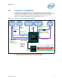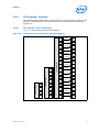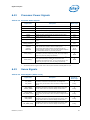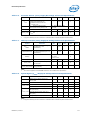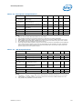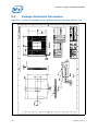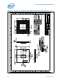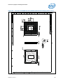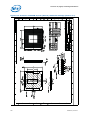
1
Mobile 3rd Generation Intel® Core™
Processor Family
Datasheet – Volume 1 of 2
June 2012
Document Number: 326768-003
INFORMATION IN THIS DOCUMENT IS PROVIDED IN CONNECTION WITH INTEL PRODUCTS. NO LICENSE, EXPRESS OR IMPLIED,
BY ESTOPPEL OR OTHERWISE, TO ANY INTELLECTUAL PROPERTY RIGHTS IS GRANTED BY THIS DOCUMENT. EXCEPT AS
PROVIDED IN INTEL'S TERMS AND CONDITIONS OF SALE FOR SUCH PRODUCTS, INTEL ASSUMES NO LIABILITY WHATSOEVER
AND INTEL DISCLAIMS ANY EXPRESS OR IMPLIED WARRANTY, RELATING TO SALE AND/OR USE OF INTEL PRODUCTS INCLUDING
LIABILITY OR WARRANTIES RELATING TO FITNESS FOR A PARTICULAR PURPOSE, MERCHANTABILITY, OR INFRINGEMENT OF ANY
PATENT, COPYRIGHT OR OTHER INTELLECTUAL PROPERTY RIGHT.
A "Mission Critical Application" is any application in which failure of the Intel Product could result, directly or indirectly, in personal
injury or death. SHOULD YOU PURCHASE OR USE INTEL'S PRODUCTS FOR ANY SUCH MISSION CRITICAL APPLICATION, YOU
SHALL INDEMNIFY AND HOLD INTEL AND ITS SUBSIDIARIES, SUBCONTRACTORS AND AFFILIATES, AND THE DIRECTORS,
OFFICERS, AND EMPLOYEES OF EACH, HARMLESS AGAINST ALL CLAIMS COSTS, DAMAGES, AND EXPENSES AND REASONABLE
ATTORNEYS' FEES ARISING OUT OF, DIRECTLY OR INDIRECTLY, ANY CLAIM OF PRODUCT LIABILITY, PERSONAL INJURY, OR DEATH
ARISING IN ANY WAY OUT OF SUCH MISSION CRITICAL APPLICATION, WHETHER OR NOT INTEL OR ITS SUBCONTRACTOR WAS
NEGLIGENT IN THE DESIGN, MANUFACTURE, OR WARNING OF THE INTEL PRODUCT OR ANY OF ITS PARTS.
Intel may make changes to specifications and product descriptions at any time, without notice. Designers must not rely on the
absence or characteristics of any features or instructions marked "reserved" or "undefined". Intel reserves these for future
definition and shall have no responsibility whatsoever for conflicts or incompatibilities arising from future changes to them. The
information here is subject to change without notice. Do not finalize a design with this information.
The products described in this document may contain design defects or errors known as errata which may cause the product to
deviate from published specifications. Current characterized errata are available on request.
This document contains information on products in the design phase of development. Do not finalize a design with this information.
Revised information will be published when the product is available. Verify with your local sales office that you have the latest
datasheet before finalizing a design.
Contact your local Intel sales office or your distributor to obtain the latest specifications and before placing your product order.
Copies of documents which have an order number and are referenced in this document, or other Intel literature, may be obtained
by calling 1-800-548-4725, or go to: http://www.intel.com/design/literature.htm.
Enabling Execute Disable Bit functionality requires a PC with a processor with Execute Disable Bit capability and a supporting
operating system. Check with your PC manufacturer on whether your system delivers Execute Disable Bit functionality.
Enhanced Intel SpeedStep® Technology; See the Processor Spec Finder or contact your Intel representative for more information.
64-bit computing on Intel architecture requires a computer system with a processor, chipset, BIOS, operating system, device
drivers and applications enabled for Intel® 64 architecture. Performance will vary depending on your hardware and software
configurations. Consult with your system vendor for more information.
No computer system can provide absolute security under all conditions. Intel® Trusted Execution Technology (Intel® TXT) requires
a computer system with Intel® Virtualization Technology, an Intel TXT-enabled processor, chipset, BIOS, Authenticated Code
Modules and an Intel TXT-compatible measured launched environment (MLE). The MLE could consist of a virtual machine monitor,
an OS or an application. In addition, Intel TXT requires the system to contain a TPM v1.2, as defined by the Trusted Computing
Group and specific software for some uses. For more information, see http://www.intel.com/technology/security/.
Intel® Virtualization Technology requires a computer system with an enabled Intel® processor, BIOS, virtual machine monitor
(VMM) and, for some uses, certain computer system software enabled for it. Functionality, performance or other benefits will vary
depending on hardware and software configurations and may require a BIOS update. Software applications may not be compatible
with all operating systems. Please check with your application vendor.
Intel® Active Management Technology requires the computer system to have an Intel® AMT-enabled chipset, network hardware
and software, as well as connection with a power source and a corporate network connection. Setup requires configuration by the
purchaser and may require scripting with the management console or further integration into existing security frameworks to
enable certain functionality. It may also require modifications of implementation of new business processes. With regard to
notebooks, Intel AMT may not be available or certain capabilities may be limited over a host OS-based VPN or when connecting
wirelessly, on battery power, sleeping, hibernating or powered off. For more information, see http://www.intel.com/technology/
platform-technology/intel-amt/.
Intel® Turbo Boost Technology requires a PC with a processor with Intel Turbo Boost Technology capability. Intel Turbo Boost
Technology performance varies depending on hardware, software and overall system configuration. Check with your PC
manufacturer on whether your system delivers Intel Turbo Boost Technology.For more information, see http://www.intel.com/
technology/turboboost.
Intel processor numbers are not a measure of performance. Processor numbers differentiate features within each processor family,
not across different processor families. See www.intel.com/products/processor_number for details.
Intel, Intel Core, and the Intel logo are trademarks of Intel Corporation in the U.S. and other countries.
*Other names and brands may be claimed as the property of others.
Copyright © 2012, Intel Corporation. All rights reserved.
2
Datasheet, Volume 1
Contents
1
Introduction ............................................................................................................ 11
1.1
Processor Feature Details ................................................................................... 13
1.1.1 Supported Technologies .......................................................................... 13
1.2
Interfaces ........................................................................................................ 13
1.2.1 System Memory Support ......................................................................... 13
1.2.2 PCI Express* ......................................................................................... 14
1.2.3 Direct Media Interface (DMI).................................................................... 15
1.2.4 Platform Environment Control Interface (PECI) ........................................... 16
1.2.5 Processor Graphics ................................................................................. 16
1.2.6 Embedded DisplayPort* (eDP*) ................................................................ 17
1.2.7 Intel® Flexible Display Interface (Intel® FDI) ............................................. 17
1.3
Power Management Support ............................................................................... 17
1.3.1 Processor Core....................................................................................... 17
1.3.2 System ................................................................................................. 17
1.3.3 Memory Controller.................................................................................. 17
1.3.4 PCI Express* ......................................................................................... 17
1.3.5 DMI...................................................................................................... 17
1.3.6 Processor Graphics Controller (GT) ........................................................... 18
1.3.7 Thermal Management Support ................................................................. 18
1.4
Mobile 3rd Generation Intel® Core™ Processor Family SKU Definition ...................... 18
1.5
Package ........................................................................................................... 18
1.6
Processor Compatibility ...................................................................................... 19
1.7
Terminology ..................................................................................................... 20
1.8
Related Documents ........................................................................................... 22
2
Interfaces................................................................................................................ 23
2.1
System Memory Interface .................................................................................. 23
2.1.1 System Memory Technology Supported ..................................................... 23
2.1.2 System Memory Timing Support............................................................... 24
2.1.3 System Memory Organization Modes......................................................... 25
2.1.3.1 Single-Channel Mode................................................................. 25
2.1.3.2 Dual-Channel Mode – Intel® Flex Memory Technology Mode ........... 25
2.1.4 Rules for Populating Memory Slots ............................................................ 26
2.1.5 Technology Enhancements of Intel® Fast Memory Access (Intel® FMA).......... 27
2.1.5.1 Just-in-Time Command Scheduling.............................................. 27
2.1.5.2 Command Overlap .................................................................... 27
2.1.5.3 Out-of-Order Scheduling ............................................................ 27
2.1.6 Data Scrambling .................................................................................... 27
2.1.7 DRAM Clock Generation........................................................................... 27
2.1.8 DDR3 Reference Voltage Generation ......................................................... 28
2.2
PCI Express* Interface....................................................................................... 28
2.2.1 PCI Express* Architecture ....................................................................... 28
2.2.1.1 Transaction Layer ..................................................................... 29
2.2.1.2 Data Link Layer ........................................................................ 29
2.2.1.3 Physical Layer .......................................................................... 29
2.2.2 PCI Express* Configuration Mechanism ..................................................... 30
2.2.3 PCI Express* Graphics ............................................................................ 31
2.2.3.1 PCI Express* Lanes Connection .................................................. 31
2.3
Direct Media Interface (DMI)............................................................................... 32
2.3.1 DMI Error Flow....................................................................................... 32
2.3.2 Processor/PCH Compatibility Assumptions.................................................. 32
Datasheet, Volume 1
3
2.4
2.5
2.6
2.3.3 DMI Link Down .......................................................................................32
Processor Graphics Controller (GT).......................................................................32
2.4.1 3D and Video Engines for Graphics Processing ............................................33
2.4.1.1 3D Engine Execution Units ..........................................................33
2.4.1.2 3D Pipeline ...............................................................................34
2.4.1.3 Video Engine ............................................................................34
2.4.1.4 2D Engine ................................................................................35
2.4.2 Processor Graphics Display ......................................................................36
2.4.2.1 Display Planes ..........................................................................36
2.4.2.2 Display Pipes ............................................................................37
2.4.2.3 Display Ports ............................................................................37
2.4.2.4 Embedded DisplayPort (eDP) ......................................................37
2.4.3 Intel® Flexible Display Interface ...............................................................37
2.4.4 Multi Graphics Controllers Multi-Monitor Support .........................................38
Platform Environment Control Interface (PECI) ......................................................38
Interface Clocking..............................................................................................38
2.6.1 Internal Clocking Requirements ................................................................38
3
Technologies............................................................................................................39
3.1
Intel® Virtualization Technology ..........................................................................39
3.1.1 Intel® VT-x Objectives ............................................................................39
3.1.2 Intel® VT-x Features ...............................................................................40
3.1.3 Intel® VT-d Objectives ............................................................................40
3.1.4 Intel® VT-d Features ...............................................................................40
3.1.5 Intel® VT-d Features Not Supported..........................................................41
3.2
Intel® Trusted Execution Technology (Intel® TXT) .................................................41
3.3
Intel® Hyper-Threading Technology .....................................................................42
3.4
Intel® Turbo Boost Technology ............................................................................42
3.4.1 Intel®Turbo Boost Technology Frequency...................................................43
3.4.2 Intel® Turbo Boost Technology Graphics Frequency.....................................43
3.5
Intel® Advanced Vector Extensions (AVX) .............................................................44
3.6
Security and Cryptography Technologies...............................................................44
3.6.1 Advanced Encryption Standard New Instructions (AES-NI) ...........................44
3.6.2 PCLMULQDQ Instruction ..........................................................................44
3.6.3 RDRAND Instruction ................................................................................45
3.7
Intel® 64 Architecture x2APIC .............................................................................45
3.8
Supervisor Mode Execution Protection (SMEP) .......................................................46
3.9
Power Aware Interrupt Routing (PAIR)..................................................................46
4
Power Management .................................................................................................47
4.1
ACPI States Supported .......................................................................................48
4.1.1 System States........................................................................................48
4.1.2 Processor Core/Package Idle States...........................................................48
4.1.3 Integrated Memory Controller States .........................................................48
4.1.4 PCI Express* Link States .........................................................................49
4.1.5 DMI States ............................................................................................49
4.1.6 Processor Graphics Controller States .........................................................49
4.1.7 Interface State Combinations ...................................................................49
4.2
Processor Core Power Management ......................................................................50
4.2.1 Enhanced Intel® SpeedStep® Technology ..................................................50
4.2.2 Low-Power Idle States.............................................................................51
4.2.3 Requesting Low-Power Idle States ............................................................52
4.2.4 Core C-states .........................................................................................53
4.2.4.1 Core C0 State ...........................................................................53
4.2.4.2 Core C1/C1E State ....................................................................53
4.2.4.3 Core C3 State ...........................................................................53
4
Datasheet, Volume 1
4.3
4.4
4.5
4.6
4.7
5
4.2.4.4 Core C6 State........................................................................... 53
4.2.4.5 Core C7 State........................................................................... 54
4.2.4.6 C-State Auto-Demotion ............................................................. 54
4.2.5 Package C-States ................................................................................... 54
4.2.5.1 Package C0 .............................................................................. 56
4.2.5.2 Package C1/C1E ....................................................................... 56
4.2.5.3 Package C3 State...................................................................... 56
4.2.5.4 Package C6 State...................................................................... 56
4.2.5.5 Package C7 State...................................................................... 57
4.2.5.6 Dynamic L3 Cache Sizing ........................................................... 57
IMC Power Management..................................................................................... 57
4.3.1 Disabling Unused System Memory Outputs ................................................ 57
4.3.2 DRAM Power Management and Initialization ............................................... 58
4.3.2.1 Initialization Role of CKE ............................................................ 59
4.3.2.2 Conditional Self-Refresh ............................................................ 59
4.3.2.3 Dynamic Power Down Operation ................................................. 60
4.3.2.4 DRAM I/O Power Management .................................................... 60
4.3.3 DDR Electrical Power Gating (EPG) ........................................................... 60
PCI Express* Power Management ........................................................................ 61
DMI Power Management..................................................................................... 61
Graphics Power Management .............................................................................. 61
4.6.1 Intel® Rapid Memory Power Management (RMPM) (also known as CxSR) ....... 61
4.6.2 Intel® Graphics Performance Modulation Technology (GPMT) ....................... 61
4.6.3 Graphics Render C-State ......................................................................... 62
4.6.4 Intel® Smart 2D Display Technology (Intel® S2DDT) .................................. 62
4.6.5 Intel® Graphics Dynamic Frequency.......................................................... 62
4.6.6 Display Power Savings Technology 6.0 (DPST) ........................................... 63
4.6.7 Automatic Display Brightness (ADB) ......................................................... 63
4.6.8 Seamless Display Refresh Rate Switching Technology (SDRRST)................... 63
Graphics Thermal Power Management .................................................................. 64
Thermal Management .............................................................................................. 65
5.1
Thermal Considerations...................................................................................... 65
5.2
Intel® Turbo Boost Technology Power Monitoring................................................... 65
5.3
Intel® Turbo Boost Technology Power Control ....................................................... 66
5.3.1 Package Power Control............................................................................ 66
5.3.2 Power Plane Control................................................................................ 68
5.3.3 Turbo Time Parameter ............................................................................ 68
5.4
Configurable TDP and Low Power Mode ................................................................ 68
5.4.1 Configurable TDP ................................................................................... 68
5.4.2 Low Power Mode .................................................................................... 69
5.5
Thermal and Power Specifications........................................................................ 70
5.6
Thermal Management Features ........................................................................... 73
5.6.1 Adaptive Thermal Monitor........................................................................ 73
5.6.1.1 TCC Activation Offset ................................................................ 74
5.6.1.2 Frequency/Voltage Control ......................................................... 74
5.6.1.3 Clock Modulation ...................................................................... 76
5.6.2 Digital Thermal Sensor............................................................................ 76
5.6.2.1 Digital Thermal Sensor Accuracy (Taccuracy)................................ 77
5.6.2.2 Fan Speed Control with Digital Thermal Sensor ............................. 77
5.6.3 PROCHOT# Signal .................................................................................. 77
5.6.3.1 Bi-Directional PROCHOT# .......................................................... 77
5.6.3.2 Voltage Regulator Protection versus PROCHOT#............................ 78
5.6.3.3 Thermal Solution Design and PROCHOT# Behavior ........................ 78
5.6.3.4 Low-Power States and PROCHOT# Behavior ................................. 78
5.6.3.5 THERMTRIP# Signal .................................................................. 79
5.6.3.6 Critical Temperature Detection ................................................... 79
Datasheet, Volume 1
5
5.6.4
5.6.5
5.6.6
On-Demand Mode ...................................................................................79
5.6.4.1 MSR Based On-Demand Mode .....................................................79
5.6.4.2 I/O Emulation-Based On-Demand Mode .......................................79
Memory Thermal Management..................................................................80
Platform Environment Control Interface (PECI) ...........................................80
6
Signal Description ....................................................................................................81
6.1
System Memory Interface ...................................................................................82
6.2
Memory Reference and Compensation ..................................................................84
6.3
Reset and Miscellaneous Signals ..........................................................................84
6.4
PCI Express*-based Interface Signals ...................................................................85
6.5
Embedded DisplayPort (eDP)...............................................................................85
6.6
Intel® Flexible Display Interface Signals ...............................................................85
6.7
Direct Media Interface (DMI) ...............................................................................86
6.8
Phase Lock Loop (PLL) Signals .............................................................................86
6.9
Test Access Points (TAP) Signals ..........................................................................86
6.10 Error and Thermal Protection...............................................................................87
6.11 Power Sequencing .............................................................................................88
6.12 Processor Power Signals .....................................................................................89
6.13 Sense Signals....................................................................................................89
6.14 Ground and NCTF ..............................................................................................90
6.15 Processor Internal Pull-Up / Pull-Down..................................................................90
7
Electrical Specifications ...........................................................................................91
7.1
Power and Ground Pins.......................................................................................91
7.2
Decoupling Guidelines ........................................................................................91
7.2.1 Voltage Rail Decoupling ...........................................................................91
7.2.2 PLL Power Supply ...................................................................................91
7.3
Voltage Identification (VID).................................................................................92
7.4
System Agent (SA) Vcc VID ................................................................................95
7.5
Reserved or Unused Signals ................................................................................95
7.6
Signal Groups ...................................................................................................96
7.7
Test Access Port (TAP) Connection .......................................................................98
7.8
Component Storage Condition Specifications (Prior to Board Attach) .........................98
7.9
DC Specifications ...............................................................................................99
7.9.1 Voltage and Current Specifications ............................................................99
7.10 Platform Environmental Control Interface (PECI) DC Specifications ......................... 106
7.10.1 PECI Bus Architecture............................................................................ 106
7.10.2 PECI DC Characteristics ......................................................................... 107
7.10.3 Input Device Hysteresis ......................................................................... 107
8
Processor Pin, Signal, and Package Information .................................................... 109
8.1
Processor Pin Assignments ................................................................................ 109
8.2
Package Mechanical Information ........................................................................ 156
9
DDR Data Swizzling................................................................................................ 165
6
Datasheet, Volume 1
Figures
1-1
1-2
2-1
2-2
2-3
2-4
2-5
2-6
2-7
4-1
4-2
4-3
4-4
5-1
5-2
7-1
7-2
8-1
8-2
8-3
8-4
8-5
8-6
8-7
8-8
8-9
8-10
8-11
8-12
8-13
8-14
Mobile Processor Platform........................................................................................ 12
Mobile Processor Compatibility Diagram .................................................................... 19
Intel® Flex Memory Technology Operation ................................................................. 26
PCI Express* Layering Diagram................................................................................ 28
Packet Flow Through the Layers ............................................................................... 29
PCI Express* Related Register Structures in the Processor ........................................... 30
PCI Express* Typical Operation 16 Lanes Mapping ...................................................... 31
Processor Graphics Controller Unit Block Diagram ....................................................... 33
Processor Display Block Diagram .............................................................................. 36
Processor Power States ........................................................................................... 47
Idle Power Management Breakdown of the Processor Cores ......................................... 51
Thread and Core C-State Entry and Exit .................................................................... 51
Package C-State Entry and Exit ................................................................................ 55
Package Power Control............................................................................................ 67
Frequency and Voltage Ordering .............................................................................. 75
Example for PECI Host-Clients Connection ............................................................... 106
Input Device Hysteresis ........................................................................................ 107
rPGA988B (Socket-G2) Pin Map.............................................................................. 109
BGA1224 Ballmap (left side) .................................................................................. 121
BGA1224 Ballmap (right side) ................................................................................ 122
BGA1023 Ballmap (left side) .................................................................................. 140
BGA1023 Ballmap (right side) ................................................................................ 141
Processor rPGA988B 2C/GT1 (G24406) Mechanical Package (Sheet 1 of 2) .................. 156
Processor rPGA988B 2C/GT1 (G24406) Mechanical Package (Sheet 2 of 2) .................. 157
Processor rPGA988B 2C/GT2 (G23867) Mechanical Package (Sheet 1 of 2) .................. 158
Processor rPGA988B 2C/GT2 (G23867) Mechanical Package (Sheet 2 of 2) .................. 159
Processor rPGA988B 4C/GT2 (E95127) Mechanical Package (Sheet 1 of 2)................... 160
Processor rPGA988B 4C/GT2 (E95127) Mechanical Package (Sheet 2 of 2)................... 161
Processor BGA1023 2C/GT1 (G24405) Mechanical Package ........................................ 162
Processor BGA1023 2C/GT2 (G23866) Mechanical Package ........................................ 163
Processor BGA1224 4C/GT2 (G26204) Mechanical Package ........................................ 164
Tables
1-1
1-2
1-3
2-1
2-2
2-3
2-4
2-5
2-6
4-1
4-2
4-3
4-4
4-5
4-6
4-7
4-8
4-9
4-10
Mobile 3rd Generation Intel® Core™ Processor Family SKUs......................................... 18
Terminology .......................................................................................................... 20
Related Documents ................................................................................................ 22
Processor Mobile DIMM Support Summary by Product ................................................. 23
Supported DDR3 /DDR3L/DDR3L-RS SO-DIMM Module Configurations .......................... 24
Supported Maximum Memory Size Per DIMM ............................................................. 24
DDR3/DDR3L/DDR3L-RS @ 1.5 V System Memory Timing Support ............................... 25
DDR3L/DDR3L-RS System Memory Timing Support..................................................... 25
Reference Clock ..................................................................................................... 38
System States ....................................................................................................... 48
Processor Core/Package State Support...................................................................... 48
Integrated Memory Controller States ........................................................................ 48
PCI Express* Link States......................................................................................... 49
DMI States ............................................................................................................ 49
Processor Graphics Controller States......................................................................... 49
G, S, and C State Combinations ............................................................................... 49
D, S, and C State Combination................................................................................. 50
Coordination of Thread Power States at the Core Level ................................................ 52
P_LVLx to MWAIT Conversion .................................................................................. 52
Datasheet, Volume 1
7
4-11
4-12
5-1
5-2
5-3
5-4
5-5
5-6
6-1
6-2
6-3
6-4
6-5
6-6
6-7
6-8
6-9
6-10
6-11
6-12
6-13
6-14
6-15
6-16
6-17
7-1
7-2
7-3
7-4
7-5
7-6
7-7
7-8
7-9
7-10
7-11
7-12
7-13
7-14
7-15
8-1
8-2
8-3
9-1
9-2
8
Coordination of Core Power States at the Package Level ..............................................55
Targeted Memory State Conditions............................................................................60
Intel® Turbo Boost Technology Package Power Control Settings ....................................67
Configurable TDP Modes ..........................................................................................69
TDP Specifications ..................................................................................................71
Junction Temperature Specification ...........................................................................71
Package Turbo Parameters.......................................................................................72
Idle Power Specifications .........................................................................................73
Signal Description Buffer Types ................................................................................81
Memory Channel A..................................................................................................82
Memory Channel B..................................................................................................83
Memory Reference and Compensation .......................................................................84
Reset and Miscellaneous Signals ...............................................................................84
PCI Express* Graphics Interface Signals ....................................................................85
Embedded Display Port Signals.................................................................................85
Intel® Flexible Display Interface ...............................................................................85
DMI – Processor to PCH Serial Interface.....................................................................86
PLL Signals ............................................................................................................86
TAP Signals............................................................................................................86
Error and Thermal Protection....................................................................................87
Power Sequencing ..................................................................................................88
Processor Power Signals ..........................................................................................89
Sense Signals ........................................................................................................89
Ground and NCTF ...................................................................................................90
Processor Internal Pull Up/Pull Down .........................................................................90
IMVP7 Voltage Identification Definition ......................................................................92
VCCSA_VID Configuration........................................................................................95
Signal Groups1.......................................................................................................96
Storage Condition Ratings........................................................................................98
Processor Core (VCC) Active and Idle Mode DC Voltage and Current Specifications ...........99
Processor Uncore (VCCIO) Supply DC Voltage and Current Specifications....................... 101
Memory Controller (VDDQ) Supply DC Voltage and Current Specifications .................... 101
System Agent (VCCSA) Supply DC Voltage and Current Specifications ......................... 101
Processor PLL (VCCPLL) Supply DC Voltage and Current Specifications......................... 102
Processor Graphics (VAXG) Supply DC Voltage and Current Specifications .................... 102
DDR3/DDR3L/DDR3L-RS Signal Group DC Specifications............................................ 103
Control Sideband and TAP Signal Group DC Specifications .......................................... 104
PCI Express* DC Specifications............................................................................... 105
eDP DC Specifications ........................................................................................... 105
PECI DC Electrical Limits........................................................................................ 107
rPGA988B Processor Pin List by Pin Name ................................................................ 110
BGA1224 Processor Ball List by Ball Name ............................................................... 123
BGA1023 Processor Ball List by Ball Name ............................................................... 142
DDR Data Swizzling Table – Channel A .................................................................... 166
DDR Data Swizzling Table for Package – Channel B ................................................... 167
Datasheet, Volume 1
Revision History
Revision
Number
001
002
Description
• Initial release
Revision Date
April 2012
• Added Mobile 3rd Generation Intel® Core™ i7-3520M, i5-3360M, i5-3320M,
i7-3667U, i5-3427U processors
• Updated Table 7-10, Processor Graphics (VAXG) Supply DC Voltage and
Current Specifications
June 2012
• Updated Section 1.2.2, PCI Express*
• Updated Section 1.5, Package
003
• Removed DDR 1066 MHz support
June 2012
• Added support for DDR3L-RS
• Updated Section 2.1.1, System Memory Technology Supported
• Updated Table 2-5, DDR3L/DDR3L-RS System Memory Timing Support
§§
Datasheet, Volume 1
9
10
Datasheet, Volume 1
Introduction
1
Introduction
The Mobile 3rd Generation Intel® Core™ processor family is the next generation of 64bit, multi-core mobile processors built on 22-nanometer process technology. The
processor is designed for a two-chip platform. The two-chip platform consists of a
processor and a Platform Controller Hub (PCH) and enables higher performance, lower
cost, easier validation, and improved x-y footprint. The processor includes Integrated
Display Engine, Processor Graphics, and an Integrated Memory Controller. The
processor is designed for mobile platforms. The Mobile 3rd Generation Intel® Core™
processor family offers either 6 or 16 graphic execution units (EUs). The number of EU
engines supported may vary between processor SKUs. The processor is offered in a
rPGA988B, BGA1224, or BGA1023 package.
The Datasheet provides DC specifications, pinout and signal definitions, interface
functional descriptions, thermal specifications, and additional feature information
pertinent to the implementation and operation of the processor on its respective
platform.
Note:
Throughout this document, the Mobile 3rd Generation Intel® Core™ processor family
may be referred to simply as “processor”.
Note:
Throughout this document, the Mobile 3rd Generation Intel® Core™ processor family
refers to the Intel® Core™ processors listed in Table 1-1.
Note:
Throughout this document, the Intel® 6/7 Series Chipset Platform Controller Hub may
also be referred to as “PCH”.
Note:
Some processor features are not available on all platforms. Refer to the processor
specification update for details.
Note:
The term “MBL” refers to mobile platforms.
Datasheet, Volume 1
11
Introduction
Figure 1-1.
Mobile Processor Platform
PCI Express* 3.0
1 x16 or 2x8
DDR3 / DDR3L / DDR3L-RS
Discrete
Graphics (PEG)
Intel®
Processor
PECI
Embedded
Display Port
Intel® Flexible
Display Interface
DMI2 x4
Serial ATA
Intel®
Management
Engine
Digital Display x 3
USB 2.0 / USB 3.01
Intel® 6/7 Series
Chipset Families
LVDS Flat Panel
Intel® HD Audio
Analog CRT
SPI Flash x 2
SMBUS 2.0
SPI
Controller Link 1
FWH
LPC
PCI Express*
WiFi / WiMax
8 PCI Express* 2.0
x1 Ports
(5 GT/s)
Super I/O
GPIO
Gigabit
Network Connection
Note:
1. USB 3.0 is supported on the Intel® 7 Series Chipset family only.
12
Datasheet, Volume 1
Introduction
1.1
Processor Feature Details
•
•
•
•
1.1.1
Four or two execution cores
A 32-KB instruction and 32-KB data first-level cache (L1) for each core
A 256-KB shared instruction/data second-level cache (L2) for each core
Up to 8-MB shared instruction/data third-level cache (L3), shared among all cores
Supported Technologies
•
•
•
•
•
•
•
•
•
•
•
•
•
•
•
•
Intel® Virtualization Technology for Directed I/O (Intel® VT-d)
Intel® Virtualization Technology (Intel® VT-x)
Intel® Active Management Technology 8.0 (Intel® AMT 8.0)
Intel® Trusted Execution Technology (Intel® TXT)
Intel® Streaming SIMD Extensions 4.1 (Intel® SSE4.1)
Intel® Streaming SIMD Extensions 4.2 (Intel® SSE4.2)
Intel® Hyper-Threading Technology
Intel® 64 Architecture
Execute Disable Bit
Intel® Turbo Boost Technology
Intel® Advanced Vector Extensions (Intel® AVX)
Advanced Encryption Standard New Instructions (AES-NI)
PCLMULQDQ Instruction
RDRAND instruction for random number generation
SMEP – Supervisor Mode Execution Protection
PAIR – Power Aware Interrupt Routing
1.2
Interfaces
1.2.1
System Memory Support
• Two channels of DDR3 / DDR3L / DDR3L-RS memory with Unbuffered Small Outline
Dual In-Line Memory Modules (SO-DIMM) with a maximum of two DIMMs per
channel
Note: 2 DIMMs per channel supported only in Quad-Core rPGA package only
• Single-channel and dual-channel memory organization modes
• Data burst length of eight for all memory organization modes
• System Memory Interface I/O Voltage of 1.35 V and 1.5 V
• DDR3, DDR3L, and DDR3L-RS DIMMs/DRAMs running at 1.5 V
• DDR3L and DDR3L-RS DIMMs/DRAMS running at 1.35 V
• Support memory configurations that mix DDR3 DIMMs/DRAMs with DDR3L/
DDR3L-RS DIMMs/DRAMs running at 1.5 V
• 64-bit wide channels
• Non-ECC, Unbuffered DDR3 / DDR3L / DDR3L-RS SO-DIMMs only
• Theoretical maximum memory bandwidth of:
— 21.3 GB/s in dual-channel mode assuming DDR3 1333 MT/s
— 25.6 GB/s in dual-channel mode assuming DDR3 1600 MT/s
Datasheet, Volume 1
13
Introduction
• Processor on-die Reference Voltage (VREF) generation for both DDR3 Read
(RDVREF) and Write (VREFDQ)
• 1Gb, 2Gb, and 4Gb DDR3 DRAM device technologies are supported
— Using 4Gb DRAM device technologies, the largest memory capacity possible is
32 GB, assuming Dual Channel Mode with four x8 dual ranked DIMM memory
configuration
• Up to 64 simultaneous open pages, 32 per channel (assuming 8 ranks of 8 bank
devices)
• Command launch modes of 1N/2N
• On-Die Termination (ODT)
• Asynchronous ODT
• Intel® Fast Memory Access (Intel® FMA):
— Just-in-Time Command Scheduling
— Command Overlap
— Out-of-Order Scheduling
1.2.2
PCI Express*
• The PCI Express* lanes (PEG[15:0] TX and RX) are fully-compliant to the PCI
Express Base Specification, Revision 3.0, including support for 8.0 GT/s transfer
speeds.
• PCI Express* supported configurations in mobile products
Configuration
1
Organization
1x8
2x4
Mobile
Graphics, I/O
2
2x8
Graphics, I/O
3
1x16
Graphics, I/O
• The port may negotiate down to narrower widths
— Support for x16/x8/x4/x2/x1 widths for a single PCI Express* mode
• 2.5 GT/s, 5.0 GT/s and 8.0 GT/s PCI Express* frequencies are supported
• Gen1 Raw bit-rate on the data pins Gen 2 Raw bit-rate on the data pins of 5.0 GT/s,
resulting in a real bandwidth per pair of 500 MB/s given the 8b/10b encoding used
to transmit data across this interface. This also does not account for packet
overhead and link maintenance.
• Maximum theoretical bandwidth on the interface of 8 GB/s in each direction
simultaneously, for an aggregate of 16 GB/s when x16 Gen 2
• Gen 3 raw bit-rate on the data pins of 8.0 GT/s, resulting in a real bandwidth per
pair of 984 MB/s using 128b/130b encoding to transmit data across this interface.
This also does not account for packet overhead and link maintenance.
• Maximum theoretical bandwidth on the interface of 16 GB/s in each direction
simultaneously, for an aggregate of 32 GB/s when x16 Gen 3
• Hierarchical PCI-compliant configuration mechanism for downstream devices
• Traditional PCI style traffic (asynchronous snooped, PCI ordering)
14
Datasheet, Volume 1
Introduction
• PCI Express* extended configuration space. The first 256 bytes of configuration
space aliases directly to the PCI Compatibility configuration space. The remaining
portion of the fixed 4-KB block of memory-mapped space above that (starting at
100h) is known as extended configuration space.
• PCI Express* Enhanced Access Mechanism. Accessing the device configuration
space in a flat memory mapped fashion.
• Automatic discovery, negotiation, and training of link out of reset
• Traditional AGP style traffic (asynchronous non-snooped, PCI-X Relaxed ordering)
• Peer segment destination posted write traffic (no peer-to-peer read traffic) in
Virtual Channel 0:
— DMI -> PCI Express* Port 0
— DMI -> PCI Express* Port 1
— PCI Express* Port 0 -> DMI
— PCI Express* Port 1 -> DMI
• 64-bit downstream address format; however, the processor never generates an
address above 64 GB (Bits 63:36 will always be zeros)
• 64-bit upstream address format; however, the processor responds to upstream
read transactions to addresses above 64 GB (addresses where any of Bits 63:36
are nonzero) with an Unsupported Request response. Upstream write transactions
to addresses above 64 GB will be dropped.
• Re-issues Configuration cycles that have been previously completed with the
Configuration Retry status
• PCI Express* reference clock is 100-MHz differential clock
• Power Management Event (PME) functions
• Dynamic width capability
• Message Signaled Interrupt (MSI and MSI-X) messages
• Polarity inversion
• Static lane numbering reversal
— Does not support dynamic lane reversal, as defined (optional) by the PCI
Express Base Specification
• Supports Half Swing “low-power/low-voltage” mode
Note:
The processor does not support PCI Express* Hot-Plug.
1.2.3
Direct Media Interface (DMI)
• DMI 2.0 support
• Four lanes in each direction
• 5 GT/s point-to-point DMI interface to PCH is supported
• Raw bit-rate on the data pins of 5.0 Gb/s, resulting in a real bandwidth per pair of
500 MB/s given the 8b/10b encoding used to transmit data across this interface.
Does not account for packet overhead and link maintenance.
• Maximum theoretical bandwidth on interface of 2 GB/s in each direction
simultaneously, for an aggregate of 4 GB/s when DMI x4
• Shares 100-MHz PCI Express* reference clock
Datasheet, Volume 1
15
Introduction
• 64-bit downstream address format; however, the processor never generates an
address above 64 GB (Bits 63:36 will always be zeros)
• 64-bit upstream address format, but the processor responds to upstream read
transactions to addresses above 64 GB (addresses where any of Bits 63:36 are
nonzero) with an Unsupported Request response. Upstream write transactions to
addresses above 64 GB will be dropped.
• Supports the following traffic types to or from the PCH:
— DMI -> DRAM
— DMI -> processor core (Virtual Legacy Wires (VLWs), Resetwarn, or MSIs only)
— Processor core -> DMI
• APIC and MSI interrupt messaging support:
— Message Signaled Interrupt (MSI and MSI-X) messages
• Downstream SMI, SCI and SERR error indication
• Legacy support for ISA regime protocol (PHOLD/PHOLDA) required for parallel port
DMA, floppy drive, and LPC bus masters
• DC coupling – no capacitors between the processor and the PCH
• Polarity inversion
• PCH end-to-end lane reversal across the link
• Supports Half Swing “low-power/low-voltage”
1.2.4
Platform Environment Control Interface (PECI)
The PECI is a one-wire interface that provides a communication channel between a
PECI client (the processor) and a PECI master. The processor supports the PECI 3.0
Specification.
1.2.5
Processor Graphics
• The Processor Graphics contains a refresh of the seventh generation graphics core
enabling substantial gains in performance and lower power consumption. Up to
16 EU support.
• Next Generation Intel Clear Video Technology HD Support is a collection of video
playback and enhancement features that improve the end user’s viewing
experience
— Encode/transcode HD content
— Playback of high definition content including Blu-ray Disc*
— Superior image quality with sharper, more colorful images
— Playback of Blu-ray disc S3D content using HDMI (V.1.4 with 3D)
• DirectX* Video Acceleration (DXVA) support for accelerating video processing
— Full AVC/VC1/MPEG2 HW Decode
• Advanced Scheduler 2.0, 1.0, XPDM support
• Windows* 7, Windows* XP, OSX, Linux OS Support
• DirectX* 11, DirectX* 10.1, DirectX* 10, DirectX* 9 support
• OpenGL* 3.0 support
16
Datasheet, Volume 1
Introduction
1.2.6
Embedded DisplayPort* (eDP*)
• Stand alone dedicated port (unlike two generations ago that shared pins with PCIe
interface)
1.2.7
Intel® Flexible Display Interface (Intel® FDI)
• For SKUs with graphics, carries display traffic from the Processor Graphics in the
processor to the legacy display connectors in the PCH
• Based on DisplayPort standard
• The two FDI links are capable of being configured to support three independent
channels, one for each display pipeline
• There are two FDI channels, each one consists of four unidirectional downstream
differential transmitter pairs:
— Scalable down to 3X, 2X, or 1X based on actual display bandwidth
requirements
— Fixed frequency 2.7 GT/s data rate
• Two sideband signals for display synchronization:
— FDI_FSYNC and FDI_LSYNC (Frame and Line Synchronization)
• One Interrupt signal used for various interrupts from the PCH:
— FDI_INT signal shared by both Intel FDI Links
• PCH supports end-to-end lane reversal across both links
• Common 100-MHz reference clock
1.3
Power Management Support
1.3.1
Processor Core
• Full support of ACPI C-states as implemented by the following processor C-states:
— C0, C1, C1E, C3, C6, C7
• Enhanced Intel SpeedStep Technology
1.3.2
System
• S0, S3, S4, S5
1.3.3
Memory Controller
• Conditional self-refresh (Intel® Rapid Memory Power Management (Intel® RMPM))
• Dynamic power down
1.3.4
PCI Express*
• L0s and L1 ASPM power management capability
1.3.5
DMI
• L0s and L1 ASPM power management capability
Datasheet, Volume 1
17
Introduction
1.3.6
Processor Graphics Controller (GT)
•
•
•
•
Rapid Memory Power Management RMPM – CxSR
Graphics Performance Modulation Technology (GPMT)
Intel Smart 2D Display Technology (Intel S2DDT)
Graphics Render C-State (RC6)
• Intel Seamless Display Refresh Rate Switching with eDP port
1.3.7
Thermal Management Support
• Digital Thermal Sensor
• Intel Adaptive Thermal Monitor
• THERMTRIP# and PROCHOT# support
• On-Demand Mode
• Open and Closed Loop Throttling
• Memory Thermal Throttling
• External Thermal Sensor (TS-on-DIMM and TS-on-Board)
• Render Thermal Throttling
• Fan speed control with DTS
1.4
Mobile 3rd Generation Intel® Core™ Processor
Family SKU Definition
Table 1-1.
Mobile 3rd Generation Intel® Core™ Processor Family SKUs
1.5
Processor
Number
TDP
(W)
IA
LFM/LPM
Frequency
IA Frequency Range
GT Frequency Range
TjMAX
(°C)
i7-3920XM
55
(Down:45;Up:65)
1900 MHz
(LPM
enabled)
2.9 GHz up to 3.8 GHz
650 MHz up to 1300 MHz
105
i7-3820QM
45
1200 MHz
2.7 GHz up to 3.7 GHz
650 MHz up to 1250 MHz
105
i7-3720QM
45
1200 MHz
2.6 GHz up to 3.6 GHz
650 MHz up to 1250 MHz
105
i7-3520M
35
1200 MHz
2.9 GHz up to 3.6 GHz
650 MHz up to 1250 MHz
105
i5-3360M
35
1200 MHz
2.8 GHz up to 3.5 GHz
650 MHz up to 1200 MHz
105
i5-3320M
35
1200 MHz
2.6 GHz up to 3.3 GHz
650 MHz up to 1200 MHz
105
i7-3667U
17
(Down:14;Up:25)
800 MHz
(LPM
enabled)
2 GHz up to 3.2 GHz
350 MHz up to 1150 MHz
105
i5-3427U
17
(Down:14;Up:25)
800 MHz
(LPM
enabled)
1.8 GHz up to 2.8 GHz
350 MHz up to 1150 MHz
105
Package
The processor is available on two packages:
• A 37.5 x 37.5 mm rPGA package (rPGA988B)
• A 31 x 24 mm BGA package (BGA1023 for dual-core processors or BGA1224 for
quad-core processors)
18
Datasheet, Volume 1
Introduction
1.6
Processor Compatibility
The Mobile 3rd Generation Intel® Core™ processor family has specific platform
requirements that differentiate it from a 2nd Generation Intel® Core™ processor family
mobile processor. Platforms intending to support both processor families need to
address the platform compatibility requirements detailed in Figure 1-2.
Mobile Processor Compatibility Diagram
VCCIO
VR
VDDQ
VR
2 x 330 µF
2 x 330 µF +
1 placeholder
VCore
VR
DDR3
DDR3/3L
VAXG
VR
SVID
Figure 1-2.
VCCIO_SEL#
2G_Core: ‘1’
3G_Core: ‘0’
Need to be disconnected
To use same Voltage!
(* 1.35 V for
BGA DC only)
*VAXG: 2 ph required for
some SKUs
PEG AC Decoupling
PEG Gen 1,2 – 100 nF
PEG Gen 1,2,3 – 220 nF
2G_Core: 1.5 V
3G_Core: 1.5 V or
1.35 V
2G_Core: 1.05 V
3G_Core: 1.05 V
VCCSA
VR
Mobile
Processor
VCCSA_VID [1:0]
PROC_SELECT#
2G_Core: ‘1’
3G_Core: ‘0’
Controls DMI
and FDI
termination
PCH
DF_TVS
Notes:
1.
2G_Core = 2nd Generation Intel® Core™ processor family mobile
2.
3G_Core = Mobile 3rd Generation Intel® Core™ processor family
Datasheet, Volume 1
19
Introduction
1.7
Terminology
Table 1-2.
Terminology (Sheet 1 of 2)
Term
BLT
Block Level Transfer
CRT
Cathode Ray Tube
DDR3
Third-generation Double Data Rate SDRAM memory technology
DDR3L
DDR3 Low Voltage
DDDR3L-RS
DDR3L Reduced Standby Power
DMA
Direct Memory Access
DMI
Direct Media Interface
DP
DisplayPort*
DTS
Digital Thermal Sensor
ECC
Error Correction Code
eDP*
Embedded DisplayPort*
Enhanced Intel®
SpeedStep® Technology
Technology that provides power management capabilities to laptops.
Execute Disable Bit
The Execute Disable bit allows memory to be marked as executable or nonexecutable, when combined with a supporting operating system. If code
attempts to run in non-executable memory the processor raises an error to the
operating system. This feature can prevent some classes of viruses or worms
that exploit buffer overrun vulnerabilities and can thus help improve the overall
security of the system. See the Intel® 64 and IA-32 Architectures Software
Developer's Manuals for more detailed information.
EU
Execution Unit
IMC
Integrated Memory Controller
Intel® 64 Technology
64-bit memory extensions to the IA-32 architecture
Intel®
DPST
Intel® Display Power Saving Technology
FDI
Intel® Flexible Display Interface
Intel
20
Description
®
Intel® TXT
Intel® Trusted Execution Technology
Intel® Virtualization
Technology
Processor virtualization which when used in conjunction with Virtual Machine
Monitor software enables multiple, robust independent software environments
inside a single platform.
Intel® VT-d
Intel® Virtualization Technology (Intel® VT) for Directed I/O. Intel VT-d is a
hardware assist, under system software (Virtual Machine Manager or operating
system) control, for enabling I/O device virtualization. Intel VT-d also brings
robust security by providing protection from errant DMAs by using DMA
remapping, a key feature of Intel VT-d.
IOV
I/O Virtualization
ITPM
Integrated Trusted Platform Module
LCD
Liquid Crystal Display
LFM
Low Frequency Mode
HFM
High Frequency Mode
LVDS
Low Voltage Differential Signaling. A high speed, low power data transmission
standard used for display connections to LCD panels.
NCTF
Non-Critical to Function. NCTF locations are typically redundant ground or noncritical reserved, so the loss of the solder joint continuity at end of life conditions
will not affect the overall product functionality.
Datasheet, Volume 1
Introduction
Table 1-2.
Terminology (Sheet 2 of 2)
Term
Description
PCH
Platform Controller Hub. The chipset with centralized platform capabilities
including the main I/O interfaces along with display connectivity, audio features,
power management, manageability, security and storage features.
PECI
Platform Environment Control Interface.
PEG
PCI Express* Graphics. External Graphics using PCI Express* Architecture. A
high-speed serial interface whose configuration is software compatible with the
existing PCI specifications.
Processor
The 64-bit, single-core or multi-core component (package).
Processor Core
The term “processor core” refers to Si die itself which can contain multiple
execution cores. Each execution core has an instruction cache, data cache, and
256-KB L2 cache. All execution cores share the L3 cache.
Processor Graphics
Intel® Processor Graphics
Rank
A unit of DRAM corresponding four to eight devices in parallel, ignoring ECC.
These devices are usually, but not always, mounted on a single side of a SODIMM.
SCI
System Control Interrupt. Used in ACPI protocol.
Storage Conditions
A non-operational state. The processor may be installed in a platform, in a tray,
or loose. Processors may be sealed in packaging or exposed to free air. Under
these conditions, processor landings should not be connected to any supply
voltages, have any I/Os biased or receive any clocks. Upon exposure to “free air”
(that is, unsealed packaging or a device removed from packaging material) the
processor must be handled in accordance with moisture sensitivity labeling
(MSL) as indicated on the packaging material.
TAC
Thermal Averaging Constant.
TDP
Thermal Design Power.
TLP
Transaction Layer Packets
VAXG
Graphics core power supply.
VCC
Processor core power supply.
VCCIO
High Frequency I/O logic power supply
VCCPLL
PLL power supply
VCCSA
System Agent (memory controller, DMI, PCIe controllers, and display engine)
power supply
VDDQ
DDR3 power supply.
VLD
Variable Length Decoding.
VSS
Processor ground.
x1
Refers to a Link or Port with one Physical Lane.
x16
Refers to a Link or Port with sixteen Physical Lanes.
x4
Refers to a Link or Port with four Physical Lanes.
x8
Refers to a Link or Port with eight Physical Lanes.
Datasheet, Volume 1
21
Introduction
1.8
Related Documents
Table 1-3.
Related Documents
Document Number/
Location
Document
Mobile 3rd Generation Intel® Core™ Processor Family Datasheet, Volume 2
326769
Mobile 3rd Generation Intel® Core™ Processor Family Specification Update
326770
Advanced Configuration and Power Interface Specification 3.0
PCI Local Bus Specification 3.0
http://www.acpi.info/
http://www.pcisig.com/speci
fications
PCI Express* Base Specification 2.0
http://www.pcisig.com
DDR3 SDRAM Specification
http://www.jedec.org
DisplayPort* Specification
http://www.vesa.org
Intel
®
64 and IA-32 Architectures Software Developer's Manuals
http://www.intel.com/produ
cts/processor/manuals/inde
x.htm
Volume 1: Basic Architecture
253665
Volume 2A: Instruction Set Reference, A-M
253666
Volume 2B: Instruction Set Reference, N-Z
253667
Volume 3A: System Programming Guide
253668
Volume 3B: System Programming Guide
253669
Note:
Contact your Intel representative for the latest revision of this item.
§§
22
Datasheet, Volume 1
Interfaces
2
Interfaces
This chapter describes the interfaces supported by the processor.
2.1
System Memory Interface
2.1.1
System Memory Technology Supported
The Integrated Memory Controller (IMC) supports DDR3 / DDR3L / DDR3L-RS protocols
with two independent, 64-bit wide channels, each accessing one or two DIMMs. The
IMC supports one or two, unbuffered non-ECC DDR3 DIMM per-channel; thus, allowing
up to four device ranks per-channel.
Note:
The processor supports only JEDEC approved memory modules and devices.
Note:
2 DIMMs per channel supported only in Quad-Core rPGA package.
Table 2-1.
Processor Mobile DIMM Support Summary by Product
Processor cores
Package
DIMM per channel
DDR3/DDR3L/
DDR3L-RS
@ 1.5 V
DDR3L/
DDR3L-RS
@ 1.35 V
Dual Core,
Quad Core
rPGA, BGA
1 DPC
1333/1600
1333/1600
Quad Core
rPGA
2 DPC
1333/1600
1333
• DDR3 / DDR3L / DDR3L-RS at 1.5 V Data Transfer Rates
— 1333 MT/s (PC3-10600), 1600 MT/s (PC3-12800)
• DDR3L / DDR3L-RS at 1.35 V Data Transfer Rates
— 1333 MT/s (PC3-10600), 1600 MT/s (PC3-12800)
• DDR3 / DDR3L / DDR3L-RS DRAM Device Technology
— Standard 1-Gb, 2-Gb, and 4-Gb technologies and addressing are supported for
x16 and x8 devices. There is no support for memory modules with different
technologies or capacities on opposite sides of the same memory module. If
one side of a memory module is populated, the other side is either identical or
empty.
Datasheet, Volume 1
23
Interfaces
Table 2-2.
Supported DDR3 /DDR3L/DDR3L-RS SO-DIMM Module Configurations
Raw
Card
Version
DIMM
Capacity
DRAM
Device
Technology
DRAM
Organization
# of
DRAM
Devices
# of
Physical
Device
Ranks
# of
Row/Col
Address
Bits
# of
Banks
Inside
DRAM
Page
Size
2 GB
2 Gb
128 M x 16
8
2
14/10
8
8K
4 GB
4 Gb
256 M x 16
8
2
15/10
8
8K
1 GB
1 Gb
128 M x 8
8
1
14/10
8
8K
2 GB
2 Gb
256 M x 8
8
1
15/10
8
8K
4 GB
4 Gb
512 M x 8
8
1
16/10
8
8K
1 GB
2 Gb
128 M x 16
4
1
14/10
8
8K
2 GB
4 Gb
256 M x 16
4
1
15/10
8
8K
2 GB
1 Gb
128 M x 8
16
2
14/10
8
8K
4 GB
2 Gb
256 M x 8
16
2
15/10
8
8K
8 GB
4 Gb
512 M x 8
16
2
16/ 10
8
8K
A
B
C
F
Note:
1.
System memory configurations are based on availability and are subject to change.
Table 2-3.
Supported Maximum Memory Size Per DIMM
Platform
Mobile
Mobile SFF
Mobile SFF
Memory Down
2.1.2
Package
rPGA
BGA
BGA
Memory
Max Size
per DIMM
[GB]
SODIMM RC A
SODIMM RC B
Max Size Per Configuration [GB]
1 Ch
1 DPC
1 Ch
2 DPC
2 Ch
1 DPC
2 Ch
2 DPC
4
4
8
8
16
4
4
8
8
16
SODIMM RC C
2
2
4
4
8
SODIMM RC F
8
8
16
16
32
SODIMM RC A
4
4
N/A
8
N/A
SODIMM RC B
4
4
N/A
8
N/A
SODIMM RC C
2
2
N/A
4
N/A
SODIMM RC F
8
8
N/A
16
N/A
MD like RC A
4
4
N/A
8
N/A
MD like RC B
4
4
N/A
8
N/A
MD like RC C
2
2
N/A
4
N/A
MD like RC F
8
8
N/A
16
N/A
System Memory Timing Support
The IMC supports the following Speed Bins, CAS Write Latency (CWL), and command
signal mode timings on the main memory interface:
•
•
•
•
•
24
tCL = CAS Latency
tRCD = Activate Command to READ or WRITE Command delay
tRP = PRECHARGE Command Period
CWL = CAS Write Latency
Command Signal modes = 1N indicates a new command may be issued every clock
and 2N indicates a new command may be issued every 2 clocks. Command launch
mode programming depends on the transfer rate and memory configuration.
Datasheet, Volume 1
Interfaces
Table 2-4.
DDR3/DDR3L/DDR3L-RS @ 1.5 V System Memory Timing Support
Segment
Extreme Edition
(XE) and
Quad Core SV
Dual Core
Standard
Voltage (SV) &
Ultra
Transfer
Rate
(MT/s)
tCL
(tCK)
tRCD
(tCK)
tRP
(tCK)
CWL
(tCK)
1333
9
9
9
7
1600
11
11
11
8
1333
9
9
9
1600
11
11
11
DPC
CMD
Mode
1
1N/2N
2
2N
1
1N/2N
2
2N
7
1
1N/2N
8
1
1N/2N
Notes1
Note:
1.
System memory timing support is based on availability and is subject to change.
Table 2-5.
DDR3L/DDR3L-RS System Memory Timing Support
Segment
Extreme Edition
(XE) and
Quad Core SV
Dual Core
Standard
Voltage (SV)
and Ultra
Transfer
Rate
(MT/s)
tCL
(tCK)
tRCD
(tCK)
tRP
(tCK)
CWL
(tCK)
1333
9
9
9
7
1600
11
11
11
8
1333
9
9
9
1600
11
11
11
DPC
CMD
Mode
1
1N/2N
2
2N
1
1N/2N
2
2N
7
1
1N/2N
8
1
1N/2N
Notes1
Notes:
1.
System memory timing support is based on availability and is subject to change.
2.1.3
System Memory Organization Modes
The IMC supports two memory organization modes, single-channel and dual-channel.
Depending upon how the DIMM Modules are populated in each memory channel, a
number of different configurations can exist.
2.1.3.1
Single-Channel Mode
In this mode, all memory cycles are directed to a single-channel. Single-channel mode
is used when either Channel A or Channel B DIMM connectors are populated in any
order, but not both.
2.1.3.2
Dual-Channel Mode – Intel® Flex Memory Technology Mode
The IMC supports Intel Flex Memory Technology Mode. Memory is divided into a
symmetric and a asymmetric zone. The symmetric zone starts at the lowest address in
each channel and is contiguous until the asymmetric zone begins or until the top
address of the channel with the smaller capacity is reached. In this mode, the system
runs with one zone of dual-channel mode and one zone of single-channel mode,
simultaneously, across the whole memory array.
Note:
Channels A and B can be mapped for physical channel 0 and 1 respectively or vice
versa; however, channel A size must be greater or equal to channel B size.
Datasheet, Volume 1
25
Interfaces
Figure 2-1.
Intel® Flex Memory Technology Operation
TOM
C
N o n in te r le a v e d
access
B
C
Dual channel
in t e r le a v e d a c c e s s
B
B
B
CH A
CH B
C H A a n d C H B c a n b e c o n fig u re d to b e p h y s ic a l c h a n n e ls 0 o r 1
B – T h e la rg e s t p h y s ic a l m e m o ry a m o u n t o f th e s m a lle r s iz e m e m o ry m o d u le
C – T h e re m a in in g p h y s ic a l m e m o ry a m o u n t o f th e la rg e r s iz e m e m o ry m o d u le
2.1.3.2.1
Dual-Channel Symmetric Mode
Dual-Channel Symmetric mode, also known as interleaved mode, provides maximum
performance on real world applications. Addresses are ping-ponged between the
channels after each cache line (64-byte boundary). If there are two requests, and the
second request is to an address on the opposite channel from the first, that request can
be sent before data from the first request has returned. If two consecutive cache lines
are requested, both may be retrieved simultaneously, since they are ensured to be on
opposite channels. Use Dual-Channel Symmetric mode when both Channel A and
Channel B DIMM connectors are populated in any order, with the total amount of
memory in each channel being the same.
When both channels are populated with the same memory capacity and the boundary
between the dual channel zone and the single channel zone is the top of memory, IMC
operates completely in Dual-Channel Symmetric mode.
Note:
The DRAM device technology and width may vary from one channel to the other.
2.1.4
Rules for Populating Memory Slots
In all System Memory Organization Modes, the frequency and latency timings of the
system memory is the lowest supported frequency and slowest supported latency
timings of all memory DIMM modules placed in the system, as determined through the
SPD registers.
26
Datasheet, Volume 1
Interfaces
2.1.5
Technology Enhancements of Intel® Fast Memory Access
(Intel® FMA)
The following sections describe the Just-in-Time Scheduling, Command Overlap, and
Out-of-Order Scheduling Intel FMA technology enhancements.
2.1.5.1
Just-in-Time Command Scheduling
The memory controller has an advanced command scheduler where all pending
requests are examined simultaneously to determine the most efficient request to be
issued next. The most efficient request is picked from all pending requests and issued
to system memory Just-in-Time to make optimal use of Command Overlapping. Thus,
instead of having all memory access requests go individually through an arbitration
mechanism forcing requests to be executed one at a time, they can be started without
interfering with the current request allowing for concurrent issuing of requests. This
allows for optimized bandwidth and reduced latency while maintaining appropriate
command spacing to meet system memory protocol.
2.1.5.2
Command Overlap
Command Overlap allows the insertion of the DRAM commands between the Activate,
Precharge, and Read/Write commands normally used, as long as the inserted
commands do not affect the currently executing command. Multiple commands can be
issued in an overlapping manner, increasing the efficiency of system memory protocol.
2.1.5.3
Out-of-Order Scheduling
While leveraging the Just-in-Time Scheduling and Command Overlap enhancements,
the IMC continuously monitors pending requests to system memory for the best use of
bandwidth and reduction of latency. If there are multiple requests to the same open
page, these requests would be launched in a back to back manner to make optimum
use of the open memory page. This ability to reorder requests on the fly allows the IMC
to further reduce latency and increase bandwidth efficiency.
2.1.6
Data Scrambling
The memory controller incorporates a DDR3 Data Scrambling feature to minimize the
impact of excessive di/dt on the platform DDR3 VRs due to successive 1s and 0s on the
data bus. Past experience has demonstrated that traffic on the data bus is not random.
Rather, it can have energy concentrated at specific spectral harmonics creating high
di/dt that is generally limited by data patterns that excite resonance between the
package inductance and on die capacitances. As a result the memory controller uses a
data scrambling feature to create pseudo-random patterns on the DDR3 data bus to
reduce the impact of any excessive di/dt.
2.1.7
DRAM Clock Generation
Every supported DIMM has two differential clock pairs. There are total of four clock
pairs driven directly by the processor to two DIMMs.
Datasheet, Volume 1
27
Interfaces
2.1.8
DDR3 Reference Voltage Generation
The processor memory controller has the capability of generating the DDR3 Reference
Voltage (VREF) internally for both read (RDVREF) and write (VREFDQ) operations. The
generated VREF can be changed in small steps, and an optimum VREF value is
determined for both during a cold boot through advanced DDR3 training procedures in
order to provide the best voltage and signal margins.
2.2
PCI Express* Interface
This section describes the PCI Express interface capabilities of the processor. See the
PCI Express Base Specification for details of PCI Express.
The processor has one PCI Express controller that can support one external x16 PCI
Express Graphics Device. The primary PCI Express Graphics port is referred to as
PEG 0.
2.2.1
PCI Express* Architecture
Compatibility with the PCI addressing model is maintained to ensure that all existing
applications and drivers may operate unchanged.
The PCI Express configuration uses standard mechanisms as defined in the PCI
Plug-and-Play specification. The processor external graphics ports support Gen 3 speed
as well. At 8 GT/s, Gen 3 operation results in twice as much bandwidth per lane as
compared to Gen 2 operation. The 16-lane PCI Express* graphics port can operate at
either 2.5 GT/s, 5 GT/s, or 8 GT/s.
PCI Express* Gen 3 uses a 128/130b encoding scheme, eliminating nearly all of the
overhead of the 8b/10b encoding scheme used in Gen 1 and Gen 2 operation.
The PCI Express architecture is specified in three layers – Transaction Layer, Data Link
Layer, and Physical Layer. The partitioning in the component is not necessarily along
these same boundaries. Refer to Figure 2-2 for the PCI Express layering diagram.
Figure 2-2.
PCI Express* Layering Diagram
Transaction
Transaction
Data Link
Data Link
Physical
Physical
Logical Sub-block
Logical Sub-block
Electrical Sub-block
Electrical Sub-block
RX
28
TX
RX
TX
Datasheet, Volume 1
Interfaces
PCI Express uses packets to communicate information between components. Packets
are formed in the Transaction and Data Link Layers to carry the information from the
transmitting component to the receiving component. As the transmitted packets flow
through the other layers, they are extended with additional information necessary to
handle packets at those layers. At the receiving side, the reverse process occurs and
packets get transformed from their Physical Layer representation to the Data Link
Layer representation and finally (for Transaction Layer Packets) to the form that can be
processed by the Transaction Layer of the receiving device.
Figure 2-3.
Packet Flow Through the Layers
Framing
Sequence
Number
Header
Data
ECRC
LCRC
Framing
Transaction Layer
Data Link Layer
Physical Layer
2.2.1.1
Transaction Layer
The upper layer of the PCI Express architecture is the Transaction Layer. The
Transaction Layer's primary responsibility is the assembly and disassembly of
Transaction Layer Packets (TLPs). TLPs are used to communicate transactions, such as
read and write, as well as certain types of events. The Transaction Layer also manages
flow control of TLPs.
2.2.1.2
Data Link Layer
The middle layer in the PCI Express stack, the Data Link Layer, serves as an
intermediate stage between the Transaction Layer and the Physical Layer.
Responsibilities of Data Link Layer include link management, error detection, and error
correction.
The transmission side of the Data Link Layer accepts TLPs assembled by the
Transaction Layer, calculates and applies data protection code and TLP sequence
number, and submits them to Physical Layer for transmission across the Link. The
receiving Data Link Layer is responsible for checking the integrity of received TLPs and
for submitting them to the Transaction Layer for further processing. On detection of TLP
error(s), this layer is responsible for requesting retransmission of TLPs until information
is correctly received, or the Link is determined to have failed. The Data Link Layer also
generates and consumes packets which are used for Link management functions.
2.2.1.3
Physical Layer
The Physical Layer includes all circuitry for interface operation, including driver and
input buffers, parallel-to-serial and serial-to-parallel conversion, PLL(s), clock recovery
circuits and impedance matching circuitry. It also includes logical functions related to
interface initialization and maintenance. The Physical Layer exchanges data with the
Data Link Layer in an implementation-specific format, and is responsible for converting
this to an appropriate serialized format and transmitting it across the PCI Express Link
at a frequency and width compatible with the remote device.
Datasheet, Volume 1
29
Interfaces
2.2.2
PCI Express* Configuration Mechanism
The PCI Express (external graphics) link is mapped through a PCI-to-PCI bridge
structure.
Figure 2-4.
PCI Express* Related Register Structures in the Processor
PCI
Express*
Device
PEG0
PCI-PCI Bridge
representing
root PCI
Express* ports
(Device 1 and
Device 6)
PCI Compatible
Host Bridge
Device
(Device 0)
DMI
PCI Express extends the configuration space to 4096 bytes per-device/function, as
compared to 256 bytes allowed by the Conventional PCI Specification. PCI Express
configuration space is divided into a PCI-compatible region (that consists of the first
256 bytes of a logical device's configuration space) and an extended PCI Express region
(that consists of the remaining configuration space). The PCI-compatible region can be
accessed using either the mechanisms defined in the PCI specification or using the
enhanced PCI Express configuration access mechanism described in the PCI Express
Enhanced Configuration Mechanism section.
The PCI Express Host Bridge is required to translate the memory-mapped PCI Express
configuration space accesses from the host processor to PCI Express configuration
cycles. To maintain compatibility with PCI configuration addressing mechanisms, it is
recommended that system software access the enhanced configuration space using
32-bit operations (32-bit aligned) only. See the PCI Express Base Specification for
details of both the PCI-compatible and PCI Express Enhanced configuration
mechanisms and transaction rules.
30
Datasheet, Volume 1
Interfaces
2.2.3
PCI Express* Graphics
The external graphics attach (PEG) on the processor is a single, 16-lane (x16) port. The
PEG port is being designed to be compliant with the PCI Express Base Specification,
Revision 3.0.
2.2.3.1
PCI Express* Lanes Connection
Figure 2-5 demonstrates the PCIe lanes mapping.
Figure 2-5.
PCI Express* Typical Operation 16 Lanes Mapping
0
1
2
3
4
5
0
Datasheet, Volume 1
7
8
9
2
10
3
11
4
12
5
13
2
6
14
3
7
15
0
1
1 X 8 Controller
1 X 4 Controller
1
1 X 16 Controller
6
Lane 0
Lane 1
Lane 2
Lane 3
Lane 4
Lane 5
Lane 6
Lane 7
Lane 8
Lane 9
Lane 10
Lane 11
Lane 12
Lane 13
Lane 14
Lane 15
0
1
2
3
4
5
6
7
8
9
10
11
12
13
14
15
31
Interfaces
2.3
Direct Media Interface (DMI)
Direct Media Interface (DMI) connects the processor and the PCH. Next generation DMI
2.0 is supported.
Note:
Only DMI x4 configuration is supported.
2.3.1
DMI Error Flow
DMI can only generate SERR in response to errors, never SCI, SMI, MSI, PCI INT, or
GPE. Any DMI related SERR activity is associated with Device 0.
2.3.2
Processor/PCH Compatibility Assumptions
The processor is compatible with the Intel 7 Series Chipset PCH products.
2.3.3
DMI Link Down
The DMI link going down is a fatal, unrecoverable error. If the DMI data link goes to
data link down, after the link was up, then the DMI link hangs the system by not
allowing the link to retrain to prevent data corruption. This link behavior is controlled
by the PCH.
Downstream transactions that had been successfully transmitted across the link prior
to the link going down may be processed as normal. No completions from downstream,
non-posted transactions are returned upstream over the DMI link after a link down
event.
2.4
Processor Graphics Controller (GT)
New Graphics Engine Architecture includes 3D compute elements, Multi-format
hardware assisted decode/encode pipeline, and Mid-Level Cache (MLC) for superior
high definition playback, video quality, and improved 3D performance and Media.
The Display Engine handles delivering the pixels to the screen, and is the primary
channel interface for display memory accesses and “PCI-like” traffic in and out.
32
Datasheet, Volume 1
Interfaces
Figure 2-6.
Processor Graphics Controller Unit Block Diagram
VS/GS
Setup/Rasterize
Hierachical Z
Hardware Clipper
Vertex
Fetch
Unified Execution Unit Array
EU
EU
EU
EU
Texture
Unit
Pixel
Backend
Additional Post Processing
Multi-Format Decode/Encode
Full MPEG2, VC1, AVC Decode
Fixed Function Post Processing
Full AVC Encode
Partial MPEG2, VC1 Encode
2.4.1
3D and Video Engines for Graphics Processing
The 3D graphics pipeline architecture simultaneously operates on different primitives or
on different portions of the same primitive. All the cores are fully programmable,
increasing the versatility of the 3D Engine. The Gen 7.0 3D engine provides the
following performance and power-management enhancements:
• Up to 16 Execution units (EUs)
• Hierarchal-Z
• Video quality enhancements
2.4.1.1
3D Engine Execution Units
• Supports up to 16 EUs. The EUs perform 128-bit wide execution per clock
• Support SIMD8 instructions for vertex processing and SIMD16 instructions for pixel
processing
Datasheet, Volume 1
33
Interfaces
2.4.1.2
3D Pipeline
2.4.1.2.1
Vertex Fetch (VF) Stage
The VF stage executes 3DPRIMITIVE commands. Some enhancements have been
included to better support legacy D3D APIs as well as SGI OpenGL*.
2.4.1.2.2
Vertex Shader (VS) Stage
The VS stage performs shading of vertices output by the VF function. The VS unit
produces an output vertex reference for every input vertex reference received from the
VF unit, in the order received.
2.4.1.2.3
Geometry Shader (GS) Stage
The GS stage receives inputs from the VS stage. Compiled application-provided GS
programs, specifying an algorithm to convert the vertices of an input object into some
output primitives. For example, a GS shader may convert lines of a line strip into
polygons representing a corresponding segment of a blade of grass centered on the
line. Or it could use adjacency information to detect silhouette edges of triangles and
output polygons extruding out from the edges.
2.4.1.2.4
Clip Stage
The Clip stage performs general processing on incoming 3D objects. However, it also
includes specialized logic to perform a Clip Test function on incoming objects. The Clip
Test optimizes generalized 3D Clipping. The Clip unit examines the position of incoming
vertices, and accepts/rejects 3D objects based on its Clip algorithm.
2.4.1.2.5
Strips and Fans (SF) Stage
The SF stage performs setup operations required to rasterize 3D objects. The outputs
from the SF stage to the Windower stage contain implementation-specific information
required for the rasterization of objects and also supports clipping of primitives to some
extent.
2.4.1.2.6
Windower/IZ (WIZ) Stage
The WIZ unit performs an early depth test, which removes failing pixels and eliminates
unnecessary processing overhead.
The Windower uses the parameters provided by the SF unit in the object-specific
rasterization algorithms. The WIZ unit rasterizes objects into the corresponding set of
pixels. The Windower is also capable of performing dithering, whereby the illusion of a
higher resolution when using low-bpp channels in color buffers is possible. Color
dithering diffuses the sharp color bands seen on smooth-shaded objects.
2.4.1.3
Video Engine
The video engine is part of the Intel Processor Graphics for image processing, playback and transcode of Video applications. The Processor Graphics video engine has a
dedicated fixed hardware pipe-line for high quality decode and encode of media
content. This engine supports Full hardware acceleration for decode of AVC/H.264,
VC-1 and MPEG -2 contents along with encode of MPEG-2 and AVC/H.264 apart from
various video processing features. The new Processor Graphics Video engine adds
support for processing features such as frame rate conversion, image stabilization, and
gamut conversion.
34
Datasheet, Volume 1
Interfaces
2.4.1.4
2D Engine
The Display Engine fetches the raw data from the memory, puts the data into a stream,
converts the data into raw pixels, organizes pixels into images, blends different planes
into a single image, encodes the data, and sends the data out to the display device.
The Display Engine executes its functions with the help of three main functional blocks
– Planes, Pipes, and Ports, except for eDP. The Planes and Pipes are in the processor
while the Ports reside in the PCH. Intel FDI connects the display engine in the processor
with the Ports in the PCH. The 2D Engine adds a new display pipe C that enables
support for three simultaneous and concurrent display configurations.
2.4.1.4.1
Processor Graphics Registers
The 2D registers consists of original VGA registers and others to support graphics
modes that have color depths, resolutions, and hardware acceleration features that go
beyond the original VGA standard.
2.4.1.4.2
Logical 128-Bit Fixed BLT and 256 Fill Engine
This BLT engine accelerates the GUI of Microsoft Windows* operating systems. The
128-bit BLT engine provides hardware acceleration of block transfers of pixel data for
many common Windows operations. The BLT engine can be used for the following:
• Move rectangular blocks of data between memory locations
• Data alignment
• To perform logical operations (raster ops)
The rectangular block of data does not change, as it is transferred between memory
locations. The allowable memory transfers are between cacheable system memory and
frame buffer memory, frame buffer memory and frame buffer memory, and within
system memory. Data to be transferred can consist of regions of memory, patterns, or
solid color fills. A pattern is always 8 x 8 pixels wide and may be 8, 16, or 32 bits per
pixel.
The BLT engine expands monochrome data into a color depth of 8, 16, or 32 bits. BLTs
can be either opaque or transparent. Opaque transfers move the data specified to the
destination. Transparent transfers compare destination color to source color and write
according to the mode of transparency selected.
Data is horizontally and vertically aligned at the destination. If the destination for the
BLT overlaps with the source memory location, the BLT engine specifies which area in
memory to begin the BLT transfer. Hardware is included for all 256 raster operations
(source, pattern, and destination) defined by Microsoft, including transparent BLT.
The BLT engine has instructions to invoke BLT and stretch BLT operations, permitting
software to set up instruction buffers and use batch processing. The BLT engine can
perform hardware clipping during BLTs.
Datasheet, Volume 1
35
Interfaces
2.4.2
Processor Graphics Display
The Processor Graphics controller display pipe can be broken down into three
components:
• Display Planes
• Display Pipes
• Embedded DisplayPort* and Intel® FDI
Figure 2-7.
Processor Display Block Diagram
VGA
Memory
Host
Interface
(Outside of
Display
Engine)
2.4.2.1
Pipe A
Plane
eDP
Mux
Panel
Fitting
Transcoder
eDP
eDP
(Tx side)
x4
FDI 0
(Tx side)
x4
FDI 1
(Tx side)
x4
Transcoder
A
Pipe B
Plane
Panel
Fitting
Transcoder
B
Pipe C
Plane
Panel
Fitting
Transcoder
C
Cross
Point
Mux
Display Planes
A display plane is a single displayed surface in memory and contains one image
(desktop, cursor, overlay). It is the portion of the display hardware logic that defines
the format and location of a rectangular region of memory that can be displayed on
display output device and delivers that data to a display pipe. This is clocked by the
Core Display Clock.
2.4.2.1.1
Primary Planes A, B, and C
Planes A, B, and C are the main display planes and are associated with Pipes A, B, and
C respectively.
2.4.2.1.2
Sprite A, B, and C
Sprite A and Sprite B are planes optimized for video decode, and are associated with
Planes A and B respectively. Sprite A and B are also double-buffered.
2.4.2.1.3
Cursors A, B, and C
Cursors A and B are small, fixed-sized planes dedicated for mouse cursor acceleration,
and are associated with Planes A and B respectively. These planes support resolutions
up to 256 x 256 each.
2.4.2.1.4
VGA
VGA is used for boot, safe mode, legacy games, and so on. It can be changed by an
application without operating system/driver notification, due to legacy requirements.
36
Datasheet, Volume 1
Interfaces
2.4.2.2
Display Pipes
The display pipe blends and synchronizes pixel data received from one or more display
planes and adds the timing of the display output device upon which the image is
displayed.
The display pipes A, B, and C operate independently of each other at the rate of 1 pixel
per clock. They can attach to any of the display ports. Each pipe sends display data to
eDP or to the PCH over the Intel Flexible Display Interface (Intel FDI).
2.4.2.3
Display Ports
The display ports consist of output logic and pins that transmit the display data to the
associated encoding logic and send the data to the display device (that is, LVDS,
HDMI*, DVI, SDVO, and so on). All display interfaces connecting external displays are
now repartitioned and driven from the PCH with the exception of the eDP DisplayPort.
Refer to the PCH datasheet for more details on display port support.
2.4.2.4
Embedded DisplayPort (eDP)
The Processor Graphics supports the Embedded Display Port (eDP) interface, intended
for display devices that are integrated into the system (such as laptop LCD panel).
DisplayPort consolidates internal and external connection methods to reduce device
complexity, support cross industry applications, and provide performance scalability.
The eDP interface supports link-speeds of 1.62 Gbps and 2.7 Gbps on 1, 2, or 4 data
lanes. The eDP supports -0.5% SSC and non-SSC clock settings.
eDP on the processor is compliant with VESA DP specification 1.1a, except the electrical
parameters that appears in chapter 7 (eDP DC Specification tables).eDP interface
supports Alternate Scrambler Seed Reset (ASSR) for eDP display authentication
thereby enabling secure transfer of protected content over the cable to sink device.
2.4.3
Intel® Flexible Display Interface
The Intel Flexible Display Interface (Intel FDI) is a proprietary link for carrying display
traffic from the Processor Graphics controller to the PCH display I/Os. Intel FDI
supports two or three independent channels – one for pipe A, one for pipe B, and one
for Pipe C.
Channels A and B have a maximum of four transmit (Tx) differential pairs used for
transporting pixel and framing data from the display engine in two display
configurations. In three display configurations Channel A has 4 transmit (Tx)
differential pairs while Channel B and C have two transmit (Tx) differential pairs.
• Each channel has four transmit (Tx) differential pairs used for transporting pixel
and framing data from the display engine
• Each channel has one single-ended LineSync and one FrameSync input (1-V CMOS
signaling)
• One display interrupt line input (1-V CMOS signaling)
• Intel FDI may dynamically scale down to 2X or 1X based on actual display
bandwidth requirements
• Common 100-MHz reference clock
• Each channel transports at a rate of 2.7 Gbps
• PCH supports end-to-end lane reversal across both channels (no reversal support
required in the processor)
Datasheet, Volume 1
37
Interfaces
2.4.4
Multi Graphics Controllers Multi-Monitor Support
The processor supports simultaneous use of the Processor Graphics Controller (GT) and
a x16 PCI Express Graphics (PEG) device.
The processor supports a maximum of 2 displays connected to the PEG card in parallel
with up to 2 displays connected to the processor and PCH.
Note:
When supporting Multi Graphics Multi Monitors, “drag and drop” between monitors and
the 2x8 PEG is not supported.
2.5
Platform Environment Control Interface (PECI)
The PECI is a one-wire interface that provides a communication channel between a
PECI client (processor) and a PECI master. The processor implements a PECI interface
to:
• Allow communication of processor thermal and other information to the PECI
master.
• Read averaged Digital Thermal Sensor (DTS) values for fan speed control.
2.6
Interface Clocking
2.6.1
Internal Clocking Requirements
Table 2-6.
Reference Clock
Reference Input Clock
Input Frequency
Associated PLL
BCLK/BCLK#
100 MHz
Processor/Memory/Graphics/PCIe/DMI/FDI
DPLL_REF_CLK/DPLL_REF_CLK#
120 MHz
Embedded DisplayPort (eDP)
§§
38
Datasheet, Volume 1
Technologies
3
Technologies
This chapter provides a high-level description of Intel technologies implemented in the
processor.
The implementation of the features may vary between the processor SKUs.
Details on the different technologies of Intel processors and other relevant external
notes are located at the Intel technology web site: http://www.intel.com/technology/.
3.1
Intel® Virtualization Technology
Intel Virtualization Technology (Intel VT) makes a single system appear as multiple
independent systems to software. This allows multiple, independent operating systems
to run simultaneously on a single system. Intel VT comprises technology components
to support virtualization of platforms based on Intel architecture microprocessors and
chipsets. Intel Virtualization Technology (Intel VT-x) added hardware support in the
processor to improve the virtualization performance and robustness. Intel Virtualization
Technology for Directed I/O (Intel VT-d) adds chipset hardware implementation to
support and improve I/O virtualization performance and robustness.
Intel VT-x specifications and functional descriptions are included in the Intel® 64 and
IA-32 Architectures Software Developer’s Manual, Volume 3B and is available at:
http://www.intel.com/products/processor/manuals/index.htm
Other VT documents can be referenced at:
http://www.intel.com/technology/virtualization/index.htm
3.1.1
Intel® VT-x Objectives
Intel VT-x provides hardware acceleration for virtualization of IA platforms. Virtual
Machine Monitor (VMM) can use Intel VT-x features to provide improved reliable
virtualized platform. By using Intel VT-x, a VMM is:
• Robust: VMMs no longer need to use paravirtualization or binary translation. This
means that they will be able to run off-the-shelf operating systems and applications
without any special steps.
• Enhanced: Intel VT enables VMMs to run 64-bit guest operating systems on IA x86
processors.
• More reliable: Due to the hardware support, VMMs can now be smaller, less
complex, and more efficient. This improves reliability and availability and reduces
the potential for software conflicts.
• More secure: The use of hardware transitions in the VMM strengthens the isolation
of VMs and further prevents corruption of one VM from affecting others on the
same system.
Datasheet, Volume 1
39
Technologies
3.1.2
Intel® VT-x Features
The processor core supports the following Intel VT-x features:
• Extended Page Tables (EPT)
— EPT is hardware assisted page table virtualization
— It eliminates VM exits from guest operating system to the VMM for shadow
page-table maintenance
• Virtual Processor IDs (VPID)
— Ability to assign a VM ID to tag processor core hardware structures (such as
TLBs)
— This avoids flushes on VM transitions to give a lower-cost VM transition time
and an overall reduction in virtualization overhead
• Guest Preemption Timer
— Mechanism for a VMM to preempt the execution of a guest operating system
after an amount of time specified by the VMM. The VMM sets a timer value
before entering a guest.
— The feature aids VMM developers in flexibility and Quality of Service (QoS)
guarantees
• Descriptor-Table Exiting
— Descriptor-table exiting allows a VMM to protect a guest operating system from
internal (malicious software based) attack by preventing relocation of key
system data structures like IDT (interrupt descriptor table), GDT (global
descriptor table), LDT (local descriptor table), and TSS (task segment selector)
— A VMM using this feature can intercept (by a VM exit) attempts to relocate
these data structures and prevent them from being tampered by malicious
software
3.1.3
Intel® VT-d Objectives
The key Intel VT-d objectives are domain-based isolation and hardware-based
virtualization. A domain can be abstractly defined as an isolated environment in a
platform to which a subset of host physical memory is allocated. Virtualization allows
for the creation of one or more partitions on a single system. This could be multiple
partitions in the same operating system, or there can be multiple operating system
instances running on the same system – offering benefits such as system
consolidation, legacy migration, activity partitioning, or security.
3.1.4
Intel® VT-d Features
The processor supports the following Intel VT-d features:
• Memory controller and processor graphics comply with Intel® VT-d 1.2 specification
• Two VT-d DMA remap engines:
— iGFX DMA remap engine
— DMI/PEG
• Support for root entry, context entry, and default context
• 39-bit guest physical address and host physical address widths
• Support for 4K page sizes only
40
Datasheet, Volume 1
Technologies
• Support for register-based fault recording only (for single entry only) and support
for MSI interrupts for faults
• Support for both leaf and non-leaf caching
• Support for boot protection of default page table
• Support for non-caching of invalid page table entries
• Support for hardware based flushing of translated but pending writes and pending
reads, on IOTLB invalidation
• Support for page-selective IOTLB invalidation
• MSI cycles (MemWr to address FEEx_xxxxh) not translated
— Translation faults result in cycle forwarding to VBIOS region (byte enables
masked for writes). Returned data may be bogus for internal agents, PEG/DMI
interfaces return unsupported request status.
• Interrupt Remapping is supported
• Queued invalidation is supported
• VT-d translation bypass address range is supported (Pass Through)
Note:
Intel VT-d Technology may not be available on all SKUs.
3.1.5
Intel® VT-d Features Not Supported
The following features are not supported by the processor with Intel VT-d:
• No support for PCIe* endpoint caching (ATS)
• No support for Intel VT-d read prefetching/snarfing (that is, translations within a
cacheline are not stored in an internal buffer for reuse for subsequent translations)
• No support for advance fault reporting
• No support for super pages
• No support for Intel VT-d translation bypass address range (such usage models
need to be resolved with VMM help in setting up the page tables correctly)
3.2
Intel® Trusted Execution Technology (Intel® TXT)
Intel Trusted Execution Technology (Intel TXT) defines platform-level enhancements
that provide the building blocks for creating trusted platforms.
The Intel TXT platform helps to provide the authenticity of the controlling environment
such that those wishing to rely on the platform can make an appropriate trust decision.
The Intel TXT platform determines the identity of the controlling environment by
accurately measuring and verifying the controlling software.
Another aspect of the trust decision is the ability of the platform to resist attempts to
change the controlling environment. The Intel TXT platform will resist attempts by
software processes to change the controlling environment or bypass the bounds set by
the controlling environment.
Intel TXT is a set of extensions designed to provide a measured and controlled launch
of system software that will then establish a protected environment for itself and any
additional software that it may execute.
Datasheet, Volume 1
41
Technologies
These extensions enhance two areas:
• The launching of the Measured Launched Environment (MLE)
• The protection of the MLE from potential corruption
The enhanced platform provides these launch and control interfaces using Safer Mode
Extensions (SMX).
The SMX interface includes the following functions:
• Measured/Verified launch of the MLE
• Mechanisms to ensure the above measurement is protected and stored in a secure
location
• Protection mechanisms that allow the MLE to control attempts to modify itself
For more information, refer to the Intel® TXT Measured Launched Environment
Developer’s Guide in http://www.intel.com/content/www/us/en/softwaredevelopers/intel-txt-software-development-guide.html.
3.3
Intel® Hyper-Threading Technology
The processor supports Intel® Hyper-Threading Technology (Intel® HT Technology)
that allows an execution core to function as two logical processors. While some
execution resources such as caches, execution units, and buses are shared, each
logical processor has its own architectural state with its own set of general-purpose
registers and control registers. This feature must be enabled using the BIOS and
requires operating system support.
Intel recommends enabling Hyper-Threading Technology with Microsoft Windows 7*,
Microsoft Windows Vista*, Microsoft Windows* XP Professional/Windows* XP Home,
and disabling Hyper-Threading Technology using the BIOS for all previous versions of
Windows operating systems. For more information on Hyper-Threading Technology, see
http://www.intel.com/technology/platform-technology/hyper-threading/.
3.4
Intel® Turbo Boost Technology
Intel Turbo Boost Technology will increase the ratio of application power to TDP. Thus,
thermal solutions and platform cooling that are designed to less than thermal design
guidance might experience thermal and performance issues since more applications will
tend to run at the maximum power limit for significant periods of time.
Note:
Intel Turbo Boost Technology may not be available on all SKUs.
Intel Turbo Boost Technology is a feature that allows the processor to opportunistically
and automatically run faster than its rated operating core and/or render clock
frequency when there is sufficient power headroom, and the product is within specified
temperature and current limits. The Intel Turbo Boost Technology feature is designed to
increase performance of both multi-threaded and single-threaded workloads. The
processor supports a Turbo mode where the processor can use the thermal capacity
associated with the package and run at power levels higher than TDP power for short
durations. This improves the system responsiveness for short, bursty usage conditions.
The turbo feature needs to be properly enabled by BIOS for the processor to operate
42
Datasheet, Volume 1
Technologies
with maximum performance. Since the turbo feature is configurable and dependent on
many platform design limits outside of the processor control, the maximum
performance cannot be ensured.
Turbo Mode availability is independent of the number of active cores; however, the
Turbo Mode frequency is dynamic and dependent on the instantaneous application
power load, the number of active cores, user configurable settings, operating
environment, and system design.
3.4.1
Intel®Turbo Boost Technology Frequency
The processor's rated frequency assumes that all execution cores are active and are at
the sustained thermal design power (TDP). However, under typical operation not all
cores are active or at executing a high power workload. Therefore, most applications
are consuming less than the TDP at the rated frequency. Intel Turbo Boost Technology
takes advantage of the available TDP headroom and active cores are able to increase
their operating frequency.
To determine the highest performance frequency amongst active cores, the processor
takes the following into consideration to recalculate turbo frequency during runtime:
• The number of cores operating in the C0 state.
• The estimated core current consumption.
• The estimated package prior and present power consumption.
• The package temperature.
Any of these factors can affect the maximum frequency for a given workload. If the
power, current, or thermal limit is reached, the processor will automatically reduce the
frequency to stay with its TDP limit. Turbo processor frequencies are only active if the
operating system is requesting the P0 state. For more information on P-states and Cstates refer to Chapter 4, “Power Management”.
3.4.2
Intel® Turbo Boost Technology Graphics Frequency
The graphics render frequency is selected dynamically based on graphics workload
demand as permitted by the processor turbo control. The processors can optimize both
processor and integrated graphics performance through power sharing. The processor
cores and the integrated graphics core share a package power limit. If the graphics
core is not consuming enough power to reach the package power limit, the cores can
increase frequency to take advantage of the unused thermal power headroom. The
opposite can happen when the processor cores are not consuming enough power to
reach the package power limit. For the integrated graphics, this could mean an increase
in the render core frequency (above its rated frequency) and increased graphics
performance. Both the processor core(s) and the graphics render core can increase
frequency higher than possible without power sharing.
Note:
The processor Utilization of turbo graphic frequencies requires that the Intel Graphics
driver to be properly installed. Turbo graphic frequencies are not dependent on the
operating system processor P-state requests and may turbo while the processor is in
any processor P-states.
Datasheet, Volume 1
43
Technologies
3.5
Intel® Advanced Vector Extensions (AVX)
Intel® Advanced Vector Extensions (AVX) is the latest expansion of the Intel instruction
set. It extends the Intel® Streaming SIMD Extensions (SSE) from 128-bit vectors to
256-bit vectors. Intel AVX addresses the continued need for vector floating-point
performance in mainstream scientific and engineering numerical applications, visual
processing, recognition, data-mining/synthesis, gaming, physics, cryptography and
other application areas.
The enhancement in Intel AVX allows for improved performance due to wider vectors,
new extensible syntax, and rich functionality including the ability to better manage,
rearrange, and sort data. In the processor, new instructions were added to allow
graphics, media and imaging applications to speed up the processing of large amount
of data by reducing the memory bandwidth and footprint. The new instructions convert
operands between single-precision floating point values and half-precision (16 bit)
floating point values.
For more information on Intel AVX, see http://www.intel.com/software/avx.
3.6
Security and Cryptography Technologies
3.6.1
Advanced Encryption Standard New Instructions (AES-NI)
The processor supports Advanced Encryption Standard New Instructions (AES-NI) that
are a set of Single Instruction Multiple Data (SIMD) instructions that enable fast and
secure data encryption and decryption based on the Advanced Encryption Standard
(AES). AES-NI are valuable for a wide range of cryptographic applications, for example:
applications that perform bulk encryption/decryption, authentication, random number
generation, and authenticated encryption. AES is broadly accepted as the standard for
both government and industry applications, and is widely deployed in various protocols.
AES-NI consists of six Intel SSE instructions. Four instructions, namely AESENC,
AESENCLAST, AESDEC, and AESDELAST facilitate high performance AES encryption and
decryption. The other two, AESIMC and AESKEYGENASSIST, support the AES key
expansion procedure. Together, these instructions provide a full hardware for support
AES, offering security, high performance, and a great deal of flexibility.
3.6.2
PCLMULQDQ Instruction
The processor supports the carry-less multiplication instruction, PCLMULQDQ.
PCLMULQDQ is a Single Instruction Multiple Data (SIMD) instruction that computes the
128-bit carry-less multiplication of two, 64-bit operands without generating and
propagating carries. Carry-less multiplication is an essential processing component of
several cryptographic systems and standards. Hence, accelerating carry-less
multiplication can significantly contribute to achieving high speed secure computing
and communication.
44
Datasheet, Volume 1
Technologies
3.6.3
RDRAND Instruction
The processor introduces a software visible random number generation mechanism
supported by a high quality entropy source. This capability will be made available to
programmers through the new RDRAND instruction. The resultant random number
generation capability is designed to comply with existing industry standards in this
regard (ANSI X9.82 and NIST SP 800-90).
Some possible usages of the new RDRAND instruction include cryptographic key
generation as used in a variety of applications including communication, digital
signatures, secure storage, and so on.
3.7
Intel® 64 Architecture x2APIC
The x2APIC architecture extends the xAPIC architecture which provides key mechanism
for interrupt delivery. This extension is intended primarily to increase processor
addressability.
Specifically, x2APIC:
• Retains all key elements of compatibility to the xAPIC architecture:
— delivery modes
— interrupt and processor priorities
— interrupt sources
— interrupt destination types
• Provides extensions to scale processor addressability for both the logical and
physical destination modes
• Adds new features to enhance performance of interrupt delivery
• Reduces complexity of logical destination mode interrupt delivery on link based
architectures
The key enhancements provided by the x2APIC architecture over xAPIC are the
following:
• Support for two modes of operation to provide backward compatibility and
extensibility for future platform innovations:
— In xAPIC compatibility mode, APIC registers are accessed through memory
mapped interface to a 4 KB page, identical to the xAPIC architecture.
— In x2APIC mode, APIC registers are accessed through Model Specific Register
(MSR) interfaces. In this mode, the x2APIC architecture provides significantly
increased processor addressability and some enhancements on interrupt
delivery.
• Increased range of processor addressability in x2APIC mode:
— Physical xAPIC ID field increases from 8 bits to 32 bits, allowing for interrupt
processor addressability up to 4 GB-1 processors in physical destination mode.
A processor implementation of x2APIC architecture can support fewer than
32 bits in a software transparent fashion.
— Logical xAPIC ID field increases from 8 bits to 32 bits. The 32-bit logical x2APIC
ID is partitioned into two sub-fields – a 16-bit cluster ID and a 16-bit logical ID
within the cluster. Consequently, ((2^20) -16) processors can be addressed in
logical destination mode. Processor implementations can support fewer than
16 bits in the cluster ID sub-field and logical ID sub-field in a software agnostic
fashion.
Datasheet, Volume 1
45
Technologies
• More efficient MSR interface to access APIC registers.
— To enhance inter-processor and self directed interrupt delivery as well as the
ability to virtualize the local APIC, the APIC register set can be accessed only
through MSR based interfaces in the x2APIC mode. The Memory Mapped IO
(MMIO) interface used by xAPIC is not supported in the x2APIC mode.
• The semantics for accessing APIC registers have been revised to simplify the
programming of frequently-used APIC registers by system software. Specifically
the software semantics for using the Interrupt Command Register (ICR) and End Of
Interrupt (EOI) registers have been modified to allow for more efficient delivery
and dispatching of interrupts.
The x2APIC extensions are made available to system software by enabling the local
x2APIC unit in the “x2APIC” mode. To benefit from x2APIC capabilities, a new operating
system and a new BIOS are both needed, with special support for the x2APIC mode.
The x2APIC architecture provides backward compatibility to the xAPIC architecture and
forward extendibility for future Intel platform innovations.
Note:
Intel x2APIC technology may not be available on all SKUs.
For more information, refer to the Intel 64 Architecture x2APIC specification at
http://www.intel.com/products/processor/manuals/
3.8
Supervisor Mode Execution Protection (SMEP)
The processor introduces a new mechanism that provides next level of system
protection by blocking malicious software attacks from user mode code when the
system is running in the highest privilege level.
This technology helps to protect from virus attacks and unwanted code to harm the
system.
For more information please refer to Intel® 64 and IA-32 Architectures Software
Developer’s Manual, Volume 3A at:
http://www.intel.com/Assets/PDF/manual/253668.pdf.
3.9
Power Aware Interrupt Routing (PAIR)
The processor added enhanced power-performance technology which routes interrupts
to threads or cores based on their sleep states. For example concerning energy
savings, it routes the interrupt to the active cores without waking the deep idle cores.
For Performance, it routes the interrupt to the idle (C1) cores without interrupting the
already heavily loaded cores. This enhancement is mostly beneficial for high interrupt
scenarios like Gigabit LAN, WLAN peripherals, and so on.
§§
46
Datasheet, Volume 1
Power Management
4
Power Management
This chapter provides information on the following power management topics:
• ACPI States
• Processor Core
• Integrated Memory Controller (IMC)
• PCI Express*
• Direct Media Interface (DMI)
• Processor Graphics Controller
Figure 4-1.
Processor Power States
G0 – Working
S0 – CPU Fully powered on
C0 – Active mode
P0
Pn
C1 – Auto halt
C1E – Auto halt, low freq, low voltage
C3 – L1/L2 caches flush, clocks off
C6 – save core states before shutdown
C7 – similar to C6, L3 flush
G1 – Sleeping
S3 cold – Sleep – Suspend To Ram (STR)
S4 – Hibernate – Suspend To Disk (STD),
Wakeup on PCH
S5 – Soft Off – no power,
Wakeup on PCH
G3 – Mechanical Off
Note: Power states availability may vary between the different SKUs
Datasheet, Volume 1
47
Power Management
4.1
ACPI States Supported
The ACPI states supported by the processor are described in this section.
4.1.1
System States
Table 4-1.
System States
State
G0/S0
G1/S3-Cold
Description
Full On
Suspend-to-RAM (STR). Context saved to memory (S3-Hot is not supported by the
processor).
G1/S4
Suspend-to-Disk (STD). All power lost (except wakeup on PCH).
G2/S5
Soft off. All power lost (except wakeup on PCH). Total reboot.
G3
Mechanical off. All power (AC and battery) removed from system.
4.1.2
Processor Core/Package Idle States
Table 4-2.
Processor Core/Package State Support
State
C0
C1
C1E
Description
Active mode, processor executing code
AutoHALT state
AutoHALT state with lowest frequency and voltage operating point
C3
Execution cores in C3 flush their L1 instruction cache, L1 data cache, and L2 cache
to the L3 shared cache. Clocks are shut off to each core
C6
Execution cores in this state save their architectural state before removing core
voltage
C7
Execution cores in this state behave similarly to the C6 state. If all execution cores
request C7, L3 cache ways are flushed until it is cleared.
4.1.3
Integrated Memory Controller States
Table 4-3.
Integrated Memory Controller States
State
Power up
Pre-charge Power Down
Active Power Down
Self-Refresh
48
Description
CKE asserted. Active mode.
CKE de-asserted (not self-refresh) with all banks closed
CKE de-asserted (not self-refresh) with minimum one bank active
CKE de-asserted using device self-refresh
Datasheet, Volume 1
Power Management
4.1.4
PCI Express* Link States
Table 4-4.
PCI Express* Link States
State
Description
L0
Full on – Active transfer state.
L0s
First Active Power Management low power state – Low exit latency
L1
Lowest Active Power Management – Longer exit latency
L3
Lowest power state (power-off) – Longest exit latency
4.1.5
DMI States
Table 4-5.
DMI States
State
Description
L0
Full on – Active transfer state
L0s
First Active Power Management low power state – Low exit latency
L1
Lowest Active Power Management – Longer exit latency
L3
Lowest power state (power-off) – Longest exit latency
4.1.6
Processor Graphics Controller States
Table 4-6.
Processor Graphics Controller States
State
Description
D0
Full on, display active
D3 Cold
Power-off
4.1.7
Interface State Combinations
Table 4-7.
G, S, and C State Combinations
Global (G)
State
Sleep
(S) State
Processor
Package
(C) State
Processor
State
System Clocks
G0
S0
C0
Full On
On
G0
S0
C1/C1E
Auto-Halt
On
Auto-Halt
G0
S0
C3
Deep Sleep
On
Deep Sleep
G0
S0
C6/C7
Deep Power
Down
On
G1
S3
Power off
Off, except RTC
Suspend to RAM
G1
S4
Power off
Off, except RTC
Suspend to Disk
G2
S5
Power off
Off, except RTC
Soft Off
G3
NA
Power off
Power off
Hard off
Datasheet, Volume 1
Description
Full On
Deep Power Down
49
Power Management
Table 4-8.
D, S, and C State Combination
Graphics Adapter
(D) State
4.2
Sleep (S) State
Package (C) State
D0
S0
C0
D0
S0
C1/C1E
Description
Full On, Displaying
Auto-Halt, Displaying
D0
S0
C3
D0
S0
C6/C7
Deep sleep, Displaying
D3
S0
Any
Not displaying
D3
S3
N/A
Not displaying, Graphics Core is
powered off
D3
S4
N/A
Not displaying, suspend to disk
Deep Power Down, Displaying
Processor Core Power Management
While executing code, Enhanced Intel SpeedStep Technology optimizes the processor’s
frequency and core voltage based on workload. Each frequency and voltage operating
point is defined by ACPI as a P-state. When the processor is not executing code, it is
idle. A low-power idle state is defined by ACPI as a C-state. In general, lower power
C-states have longer entry and exit latencies.
4.2.1
Enhanced Intel® SpeedStep® Technology
The following are the key features of Enhanced Intel SpeedStep Technology:
• Multiple frequency and voltage points for optimal performance and power
efficiency. These operating points are known as P-states.
• Frequency selection is software controlled by writing to processor MSRs. The
voltage is optimized based on the selected frequency and the number of active
processor cores.
— If the target frequency is higher than the current frequency, VCC is ramped up
in steps to an optimized voltage. This voltage is signaled by the SVID bus to the
voltage regulator. Once the voltage is established, the PLL locks on to the
target frequency.
— If the target frequency is lower than the current frequency, the PLL locks to the
target frequency, then transitions to a lower voltage by signaling the target
voltage on SVID bus.
— All active processor cores share the same frequency and voltage. In a multicore processor, the highest frequency P-state requested amongst all active
cores is selected.
— Software-requested transitions are accepted at any time. If a previous
transition is in progress, the new transition is deferred until the previous
transition is completed.
• The processor controls voltage ramp rates internally to ensure glitch-free
transitions.
• Because there is low transition latency between P-states, a significant number of
transitions per-second are possible.
50
Datasheet, Volume 1
Power Management
4.2.2
Low-Power Idle States
When the processor is idle, low-power idle states (C-states) are used to save power.
More power savings actions are taken for numerically higher C-states. However, higher
C-states have longer exit and entry latencies. Resolution of C-states occur at the
thread, processor core, and processor package level. Thread-level C-states are
available if Intel Hyper-Threading Technology is enabled.
Caution:
Figure 4-2.
Long term reliability cannot be assured unless all the Low Power Idle States are
enabled.
Idle Power Management Breakdown of the Processor Cores
Thread 0
Thread 1
Thread 0
Core 0 State
Thread 1
Core 1 State
Processor Package State
Entry and exit of the C-States at the thread and core level are shown in Figure 4-3.
Figure 4-3.
Thread and Core C-State Entry and Exit
C0
MWAIT(C1), HLT
MWAIT(C1), HLT
(C1E Enabled)
C1
C1E
MWAIT(C7),
P_LVL4 I/O Read
MWAIT(C3),
P_LVL2 I/O Read
C3
MWAIT(C6),
P_LVL3 I/O Read
C6
C7
While individual threads can request low power C-states, power saving actions only
take place once the core C-state is resolved. Core C-states are automatically resolved
by the processor. For thread and core C-states, a transition to and from C0 is required
before entering any other C-state.
Datasheet, Volume 1
51
Power Management
Table 4-9.
Coordination of Thread Power States at the Core Level
Processor Core
C-State
C0
C1
C3
C6
C7
C0
C0
C0
C0
C0
C1
C0
C11
C11
C11
C11
C3
C0
C11
C3
C3
C3
C6
C0
C1
1
C3
C6
C6
C7
C0
C11
C3
C6
C7
C0
Thread 0
Note:
4.2.3
Thread 1
If enabled, the core C-state will be C1E if all cores have resolved a core C1 state or higher.
Requesting Low-Power Idle States
The primary software interfaces for requesting low power idle states are through the
MWAIT instruction with sub-state hints and the HLT instruction (for C1 and C1E).
However, software may make C-state requests using the legacy method of I/O reads
from the ACPI-defined processor clock control registers, referred to as P_LVLx. This
method of requesting C-states provides legacy support for operating systems that
initiate C-state transitions using I/O reads.
To seamless support of legacy operating systems, P_LVLx I/O reads are converted
within the processor to the equivalent MWAIT C-state request. Therefore, P_LVLx reads
do not directly result in I/O reads to the system. The feature, known as I/O MWAIT
redirection, must be enabled in the BIOS.
Note:
The P_LVLx I/O Monitor address needs to be set up before using the P_LVLx I/O read
interface. Each P-LVLx is mapped to the supported MWAIT(Cx) instruction as shown in
Table 4-10.
Table 4-10. P_LVLx to MWAIT Conversion
P_LVLx
MWAIT(Cx)
Notes
P_LVL2
MWAIT(C3)
P_LVL3
MWAIT(C6)
C6. No sub-states allowed.
P_LVL4
MWAIT(C7)
C7. No sub-states allowed.
P_LVL5+
MWAIT(C7)
C7. No sub-states allowed.
The BIOS can write to the C-state range field of the PMG_IO_CAPTURE MSR to restrict
the range of I/O addresses that are trapped and emulate MWAIT like functionality. Any
P_LVLx reads outside of this range does not cause an I/O redirection to an MWAIT(Cx)like request. They fall through like a normal I/O instruction.
Note:
52
When P_LVLx I/O instructions are used, MWAIT substates cannot be defined. The
MWAIT substate is always zero if I/O MWAIT redirection is used. By default, P_LVLx I/O
redirections enable the MWAIT 'break on EFLAGS.IF’ feature that triggers a wakeup on
an interrupt even if interrupts are masked by EFLAGS.IF.
Datasheet, Volume 1
Power Management
4.2.4
Core C-states
The following are general rules for all core C-states, unless specified otherwise:
• A core C-State is determined by the lowest numerical thread state (such as Thread
0 requests C1E while Thread 1 requests C3, resulting in a core C1E state). See
Table 4-7.
• A core transitions to C0 state when:
— An interrupt occurs
— There is an access to the monitored address if the state was entered using an
MWAIT instruction
• For core C1/C1E, core C3, and core C6/C7, an interrupt directed toward a single
thread wakes only that thread. However, since both threads are no longer at the
same core C-state, the core resolves to C0.
• A system reset re-initializes all processor cores
4.2.4.1
Core C0 State
The normal operating state of a core where code is being executed.
4.2.4.2
Core C1/C1E State
C1/C1E is a low power state entered when all threads within a core execute a HLT or
MWAIT(C1/C1E) instruction.
A System Management Interrupt (SMI) handler returns execution to either Normal
state or the C1/C1E state. See the Intel® 64 and IA-32 Architecture Software
Developer’s Manual, Volume 3A/3B: System Programmer’s Guide for more information.
While a core is in C1/C1E state, it processes bus snoops and snoops from other
threads. For more information on C1E, see “Package C1/C1E”.
4.2.4.3
Core C3 State
Individual threads of a core can enter the C3 state by initiating a P_LVL2 I/O read to
the P_BLK or an MWAIT(C3) instruction. A core in C3 state flushes the contents of its
L1 instruction cache, L1 data cache, and L2 cache to the shared L3 cache, while
maintaining its architectural state. All core clocks are stopped at this point. Because the
core’s caches are flushed, the processor does not wake any core that is in the C3 state
when either a snoop is detected or when another core accesses cacheable memory.
4.2.4.4
Core C6 State
Individual threads of a core can enter the C6 state by initiating a P_LVL3 I/O read or an
MWAIT(C6) instruction. Before entering core C6, the core will save its architectural
state to a dedicated SRAM. Once complete, a core will have its voltage reduced to zero
volts. During exit, the core is powered on and its architectural state is restored.
Datasheet, Volume 1
53
Power Management
4.2.4.5
Core C7 State
Note:
The terms “Core C6 state” and “Core C7 state” defines the same individual core power
state. In both cases the processor cores that request either C6 or C7 will enter the C6
state.
Individual threads of a core can enter the C7 state by initiating a P_LVL4 I/O read to
the P_BLK or by an MWAIT(C7) instruction. The core C7 state exhibits the same
behavior as the core C6 state unless the core is the last one in the package to enter the
C7 state. If it is, that core is responsible for flushing L3 cache ways. The processor
supports the C7s substate. When an MWAIT(C7) command is issued with a C7s
sub-state hint, the entire L3 cache is flushed one step as opposed to flushing the L3
cache in multiple steps.
4.2.4.6
C-State Auto-Demotion
In general, deeper C-states such as C6 or C7 have long latencies and have higher
energy entry/exit costs. The resulting performance and energy penalties become
significant when the entry/exit frequency of a deeper C-state is high. Therefore,
incorrect or inefficient usage of deeper C-states have a negative impact on battery life.
To increase residency and improve battery life in deeper C-states, the processor
supports C-state auto-demotion.
There are two C-State auto-demotion options:
• C7/C6 to C3
• C7/C6/C3 To C1
The decision to demote a core from C6/C7 to C3 or C3/C6/C7 to C1 is based on each
core’s immediate residency history. Upon each core C6/C7 request, the core C-state is
demoted to C3 or C1 until a sufficient amount of residency has been established. At
that point, a core is allowed to go into C3/C6 or C7. Each option can be run
concurrently or individually.
This feature is disabled by default. BIOS must enable it in the
PMG_CST_CONFIG_CONTROL register. The auto-demotion policy is also configured by
this register.
4.2.5
Package C-States
The processor supports C0, C1/C1E, C3, C6, and C7 power states. The following is a
summary of the general rules for package C-state entry. These apply to all package Cstates unless specified otherwise:
• A package C-state request is determined by the lowest numerical core C-state
amongst all cores.
• A package C-state is automatically resolved by the processor depending on the
core idle power states and the status of the platform components.
— Each core can be at a lower idle power state than the package if the platform
does not grant the processor permission to enter a requested package C-state.
— The platform may allow additional power savings to be realized in the
processor.
— For package C-states, the processor is not required to enter C0 before entering
any other C-state.
54
Datasheet, Volume 1
Power Management
The processor exits a package C-state when a break event is detected. Depending on
the type of break event, the processor does the following:
• If a core break event is received, the target core is activated and the break event
message is forwarded to the target core.
— If the break event is not masked, the target core enters the core C0 state and
the processor enters package C0.
• If the break event was due to a memory access or snoop request.
— But the platform did not request to keep the processor in a higher package Cstate, the package returns to its previous C-state.
— And the platform requests a higher power C-state, the memory access or snoop
request is serviced and the package remains in the higher power C-state.
Table 4-11 shows package C-state resolution for a dual-core processor. Figure 4-4
summarizes package C-state transitions.
Table 4-11. Coordination of Core Power States at the Package Level
Core 1
Package C-State
C0
Note:
Figure 4-4.
C1
C3
C6
C7
C0
C0
C0
C0
C0
C1
1
C0
C1
1
C3
C3
C3
C6
C0
C11
C3
C6
C6
C7
C0
C11
C3
C6
C7
C1
Core 0
C0
C0
C3
C1
1
C1
1
C11
If enabled, the package C-state will be C1E if all cores have resolved a core C1 state or higher.
Package C-State Entry and Exit
C0
C3
C1
Datasheet, Volume 1
C6
C7
55
Power Management
4.2.5.1
Package C0
Package C0 is the normal operating state for the processor. The processor remains in
the normal state when at least one of its cores is in the C0 or C1 state or when the
platform has not granted permission to the processor to go into a low power state.
Individual cores may be in lower power idle states while the package is in C0.
4.2.5.2
Package C1/C1E
No additional power reduction actions are taken in the package C1 state. However, if
the C1E sub-state is enabled, the processor automatically transitions to the lowest
supported core clock frequency, followed by a reduction in voltage.
The package enters the C1 low power state when:
• At least one core is in the C1 state
• The other cores are in a C1 or lower power state
The package enters the C1E state when:
• All cores have directly requested C1E using MWAIT(C1) with a C1E sub-state hint
• All cores are in a power state lower that C1/C1E but the package low power state is
limited to C1/C1E using the PMG_CST_CONFIG_CONTROL MSR
• All cores have requested C1 using HLT or MWAIT(C1) and C1E auto-promotion is
enabled in IA32_MISC_ENABLES
No notification to the system occurs upon entry to C1/C1E.
4.2.5.3
Package C3 State
A processor enters the package C3 low power state when:
• At least one core is in the C3 state
• The other cores are in a C3 or lower power state, and the processor has been
granted permission by the platform
• The platform has not granted a request to a package C6/C7 state but has allowed a
package C6 state
In package C3-state, the L3 shared cache is valid.
4.2.5.4
Package C6 State
A processor enters the package C6 low power state when:
• At least one core is in the C6 state
• The other cores are in a C6 or lower power state and the processor has been
granted permission by the platform
• The platform has not granted a package C7 request but has allowed a C6 package
state.
In package C6 state, all cores have saved their architectural state and have had their
core voltages reduced to zero volts. The L3 shared cache is still powered and snoopable
in this state. The processor remains in package C6 state as long as any part of the L3
cache is active.
56
Datasheet, Volume 1
Power Management
4.2.5.5
Package C7 State
The processor enters the package C7 low power state when all cores are in the C7 state
and the L3 cache is completely flushed. The last core to enter the C7 state begins to
shrink the L3 cache by N-ways until the entire L3 cache has been emptied. This allows
further power savings.
Core break events are handled the same way as in package C3 or C6. However, snoops
are not sent to the processor in package C7 state because the platform, by granting the
package C7 state, has acknowledged that the processor possesses no snoopable
information. This allows the processor to remain in this low power state and maximize
its power savings.
Upon exit of the package C7 state, the L3 cache is not immediately re-enabled. It
re-enables once the processor has stayed out of the C6 or C7 state for a preset amount
of time. Power is saved since this prevents the L3 cache from being re-populated only
to be immediately flushed again.
4.2.5.6
Dynamic L3 Cache Sizing
Upon entry into the package C7 state, the L3 cache is reduced by N-ways until it is
completely flushed. The number of ways, N, is dynamically chosen per concurrent C7
entry. Similarly, upon exit, the L3 cache is gradually expanded based on internal
heuristics.
4.3
IMC Power Management
The main memory is power managed during normal operation and in low-power ACPI
Cx states.
4.3.1
Disabling Unused System Memory Outputs
Any System Memory (SM) interface signal that goes to a memory module connector in
which it is not connected to any actual memory devices (such as SO-DIMM connector is
unpopulated, or is single-sided) is tri-stated. The benefits of disabling unused SM
signals are:
• Reduced power consumption
• Reduced possible overshoot/undershoot signal quality issues seen by the processor
I/O buffer receivers caused by reflections from potentially un-terminated
transmission lines
When a given rank is not populated, the corresponding chip select and CKE signals are
not driven.
At reset, all rows must be assumed to be populated, until it can be proven that they are
not populated. This is due to the fact that when CKE is tri-stated with a SO-DIMM
present, the SO-DIMM is not ensured to maintain data integrity.
SCKE tri-state should be enabled by BIOS where appropriate, since at reset all rows
must be assumed to be populated.
Datasheet, Volume 1
57
Power Management
4.3.2
DRAM Power Management and Initialization
The processor implements extensive support for power management on the SDRAM
interface. There are four SDRAM operations associated with the Clock Enable (CKE)
signals that the SDRAM controller supports. The processor drives four CKE pins to
perform these operations.
The CKE is one means of power saving. When CKE is off, the internal DDR clock is
disabled and the DDR power is reduced. The power-saving differs according to the
selected mode and the DDR type used. For more information, refer to the IDD table in
the DDR specificaiton.
The DDR defines 3 levels of power down that differ in power saving and in wakeup
time:
1. Active power down (APD): This mode is entered if there are open pages when deasserting CKE. In this mode the open pages are retained. Power-saving in this
mode is the lowest. Power consumption of DDR is defined by IDD3P. Exiting this
mode is defined by tXP – small number of cycles.
2. Precharged power down (PPD): This mode is entered if all banks in DDR are
precharged when de-asserting CKE. Power-saving in this mode is intermediate –
better than APD, but less than DLL-off. Power consumption is defined by IDD2P1.
Exiting this mode is defined by tXP. The difference relative to APD mode is that
when waking-up in PPD mode, all page-buffers are empty.
3. DLL-off: In this mode the data-in DLLs on DDR are off. Power-saving in this mode is
the best among all power modes. Power consumption is defined by IDD2P1. Exiting
this mode is defined by tXP and tXPDLL (10–20 according to the DDR type) until
first data transfer is allowed.
The processor supports 6 different types of power down. The different modes are the
power down modes supported by DDR3 and combinations of these. The type of CKE
power down is defined by configuration. The options are as follows:
1. No power down
2. APD: The rank enters power down as soon as the idle-timer expires, independent of
the bank status
3. PPD: When idle timer expires, the MC sends PRE-all to rank and then enters power
down
4. DLL-off: Same as option 2 but DDR is configured to DLL-off
5. APD, change to PPD (APD-PPD): Begins as option 1, and when all page-close timers
of the rank are expired, it wakes the rank, issues PRE-all, and returns to PPD.
6. APD, change to DLL-off (APD_DLLoff): Begins as option 1, and when all page-close
timers of the rank are expired, it wakes the rank, issues PRE-all, and returns to
DLL-off power down.
The CKE is determined per rank, when it is inactive. Each rank has an idle counter. The
idle counter starts counting as soon as the rank has no accesses, and if it expires, the
rank may enter power down while no new transactions to the rank arrive to queues.
The idle counter begins counting at the last incoming transaction arrival.
58
Datasheet, Volume 1
Power Management
It is important to understand that since the power down decision is per rank, the MC
can find a lot of opportunities to power down ranks, even while running memory
intensive applications; savings may be significant (up to a few Watts, depending on
DDR configuration). This becomes more significant when each channel is populated
with more ranks.
Selection of power modes should be according to power performance or thermal tradeoffs of a given system:
• When trying to achieve maximum performance and power or thermal consideration
is a non-issue, use no power down.
• In a system that tries to minimize power-consumption, try to use the deepest
power down mode possible – DLL-off or APD_DLLoff.
• In high-performance systems with dense packaging (that is, tricky thermal design)
the power down mode should be considered in order to reduce the heating and
avoid DDR throttling caused by the heating.
Control of the power-mode through CRB-BIOS: BIOS selects by default no-power
down.
Another control is the idle timer expiration count. This is set through PM_PDWN_config
bits 7:0 (MCHBAR +4CB0). As this timer is set to a shorter time, the IMC will have
more opportunities to put DDR in power down. The minimum recommended value for
this register is 15. There is no BIOS hook to set this register. Customers who choose to
change the value of this register can do it by changing the BIOS. For experiments, this
register can be modified in real time if BIOS did not lock the MC registers.
Note:
In APD, APD-PPD, and APD-DLLoff there is no point in setting the idle counter in the
same range of page-close idle timer.
Another option associated with CKE power down is the S_DLL-off. When this option is
enabled, the SBR I/O slave DLLs go off when all channel ranks are in power down. (Do
not confuse it with the DLL-off mode, in which the DDR DLLs are off). This mode
requires an I/O slave DLL wakeup time be defined.
4.3.2.1
Initialization Role of CKE
During power-up, CKE is the only input to the SDRAM that has its level recognized
(other than the DDR3 reset pin) once power is applied. The signal must be driven LOW
by the DDR controller to make sure the SDRAM components float DQ and DQS during
power-up. CKE signals remain LOW (while any reset is active) until the BIOS writes to a
configuration register. Using this method, CKE is ensured to remain inactive for much
longer than the specified 200 μs after power and clocks to SDRAM devices are stable.
4.3.2.2
Conditional Self-Refresh
Intel Rapid Memory Power Management (Intel RMPM) conditionally places memory into
self-refresh in the package C3, C6, and C7 low-power states. RMPM functionality
depends on graphics/display state (relevant only when processor graphics is being
used), as well as memory traffic patterns generated by other connected I/O devices.
When entering the S3 - Suspend-to-RAM (STR) state or S0 conditional self-refresh, the
processor core flushes pending cycles and then enters all SDRAM ranks into self
refresh. the CKE signals remain LOW so the SDRAM devices perform self-refresh.
Datasheet, Volume 1
59
Power Management
The target behavior is to enter self-refresh for the package C3, C6, and C7 states as
long as there are no memory requests to service.
Table 4-12. Targeted Memory State Conditions
Mode
Memory State with Processor Graphics
Memory State with External Graphics
C0, C1, C1E
Dynamic memory rank power down based on
idle conditions.
Dynamic memory rank power down based on
idle conditions.
If the processor graphics engine is idle and
there are no pending display requests, then
enter self-refresh. Otherwise use dynamic
memory rank power down based on idle
conditions.
If there are no memory requests, then enter
self-refresh. Otherwise use dynamic memory
rank power down based on idle conditions.
S3
Self-Refresh Mode.
Self-Refresh Mode.
S4
Memory power down (contents lost).
Memory power down (contents lost)
C3, C6, C7
4.3.2.3
Dynamic Power Down Operation
Dynamic power down of memory is employed during normal operation. Based on idle
conditions, a given memory rank may be powered down. The IMC implements
aggressive CKE control to dynamically put the DRAM devices in a power down state.
The processor core controller can be configured to put the devices in active power down
(CKE de-assertion with open pages) or precharge power down (CKE de-assertion with
all pages closed). Precharge power down provides greater power savings but has a
bigger performance impact, since all pages will first be closed before putting the
devices in power down mode.
If dynamic power down is enabled, all ranks are powered up before doing a refresh
cycle and all ranks are powered down at the end of refresh.
4.3.2.4
DRAM I/O Power Management
Unused signals should be disabled to save power and reduce electromagnetic
interference. This includes all signals associated with an unused memory channel.
Clocks can be controlled on a per SO-DIMM basis. Exceptions are made for per SODIMM control signals such as CS#, CKE, and ODT for unpopulated SO-DIMM slots.
The I/O buffer for an unused signal should be tri-stated (output driver disabled), the
input receiver (differential sense-amp) should be disabled, and any DLL circuitry
related ONLY to unused signals should be disabled. The input path must be gated to
prevent spurious results due to noise on the unused signals (typically handled
automatically when input receiver is disabled).
4.3.3
DDR Electrical Power Gating (EPG)
The DDR I/O of the processor supports on-die Electrical Power Gating (DDR-EPG)
during normal operation (S0 mode) while the processor is at package C3 or deeper
power state.
During EPG, the VCCIO internal voltage rail will be powered down, while VDDQ and the
un-gated VCCIO will stay powered on.
The processor will transition in and out of DDR EPG mode on an as needed basis
without any external pins or signals.
60
Datasheet, Volume 1
Power Management
There is no change to the signals driven by the processor to the DIMMs during DDR IO
EPG mode.
During EPG mode, all the DDR IO logic will be powered down, except for the Physical
Control registers that are powered by the un-gated VCCIO power supply.
Unlike S3 exit, at DDR EPG exit, the DDR will not go through training mode. Rather, it
will use the previous training information retained in the physical control registers and
will immediately resume normal operation.
4.4
PCI Express* Power Management
• Active power management support using L0s and L1 states.
• All inputs and outputs disabled in L2/L3 Ready state.
Note:
PCIe* interface does not support Hot-Plug.
Note:
An increase in power consumption may be observed when PCIe ASPM capabilities are
disabled.
4.5
DMI Power Management
• Active power management support using L0s/L1 state.
4.6
Graphics Power Management
4.6.1
Intel® Rapid Memory Power Management (RMPM) (also
known as CxSR)
The Intel Rapid Memory Power Management puts rows of memory into self-refresh
mode during C3/C6/C7 to allow the system to remain in the lower power states longer.
Processors routinely save power during runtime conditions by entering the C3, C6, or
C7 state. Intel RMPM is an indirect method of power saving that can have a significant
effect on the system as a whole.
4.6.2
Intel® Graphics Performance Modulation Technology
(GPMT)
Intel Graphics Power Modulation Technology (Intel® GPMT) is a method for saving
power in the graphics adapter while continuing to display and process data in the
adapter. This method will switch the render frequency and/or render voltage
dynamically between higher and lower power states supported on the platform based
on render engine workload. When the system is running in battery mode, and if the end
user launches applications such as 3D or Video, the graphics software may switch the
render frequency dynamically between higher and lower power/performance states
depending on the render engine workload.
In products where Intel® Graphics Dynamic Frequency (also known as Turbo Boost
Technology) is supported and enabled, the functionality of Intel GPMT will be
maintained by Intel Graphics Dynamic Frequency (also known as Turbo Boost
Technology).
Datasheet, Volume 1
61
Power Management
4.6.3
Graphics Render C-State
Render C-State (RC6) is a technique designed to optimize the average power to the
graphics render engine during times of idleness of the render engine. Render C-state is
entered when the graphics render engine, blitter engine and the video engine have no
workload being currently worked on and no outstanding graphics memory transactions.
When the idleness condition is met then the Integrated Graphics will program the VR
into a low voltage state (~0V) through the SVID bus.
Caution:
Long term reliability cannot be assured unless all the Low Power Idle States are
enabled.
4.6.4
Intel® Smart 2D Display Technology (Intel® S2DDT)
Intel S2DDT reduces display refresh memory traffic by reducing memory reads
required for display refresh. Power consumption is reduced by less accesses to the IMC.
S2DDT is only enabled in single pipe mode.
Intel S2DDT is most effective with:
• Display images well suited to compression, such as text windows, slide shows, and
so on. Poor examples are 3D games.
• Static screens such as screens with significant portions of the background showing
2D applications, processor benchmarks, and so on, or conditions when the
processor is idle. Poor examples are full-screen 3D games and benchmarks that flip
the display image at or near display refresh rates.
4.6.5
Intel® Graphics Dynamic Frequency
Intel Graphics Dynamic Frequency Technology is the ability of the processor and
graphics cores to opportunistically increase frequency and/or voltage above the
ensured processor and graphics frequency for the given part. Intel Graphics Dynamic
Frequency Technology is a performance feature that makes use of unused package
power and thermals to increase application performance. The increase in frequency is
determined by how much power and thermal budget is available in the package, and
the application demand for additional processor or graphics performance. The
processor core control is maintained by an embedded controller. The graphics driver
dynamically adjusts between P-States to maintain optimal performance, power, and
thermals.
62
Datasheet, Volume 1
Power Management
4.6.6
Display Power Savings Technology 6.0 (DPST)
This is a mobile only supported power management feature.
The Intel DPST technique achieves backlight power savings while maintaining a good
visual experience. This is accomplished by adaptively enhancing the displayed image
while decreasing the backlight brightness simultaneously. The goal of this technique is
to provide equivalent end-user-perceived image quality at a decreased backlight power
level.
1. The original (input) image produced by the operating system or application is
analyzed by the Intel DPST subsystem. An interrupt to Intel DPST software is
generated whenever a meaningful change in the image attributes is detected. (A
meaningful change is when the Intel DPST software algorithm determines that
enough brightness, contrast, or color change has occurred to the displaying images
that the image enhancement and backlight control needs to be altered.)
2. Intel DPST subsystem applies an image-specific enhancement to increase image
contrast, brightness, and other attributes.
3. A corresponding decrease to the backlight brightness is applied simultaneously to
produce an image with similar user-perceived quality (such as brightness) as the
original image.
Intel® DPST 5.0 has improved the software algorithms and has minor hardware
changes to better handle backlight phase-in and ensures the documented and validated
method to interrupt hardware phase-in.
4.6.7
Automatic Display Brightness (ADB)
This is a mobile only supported power management feature.
The Intel Automatic Display Brightness feature dynamically adjusts the backlight
brightness based upon the current ambient light environment. This feature requires an
additional sensor to be on the panel front. The sensor receives the changing ambient
light conditions and sends the interrupts to the Intel Graphics driver. As per the change
in Lux, (current ambient light illuminance), the new backlight setting can be adjusted
through BLC. The converse applies for a brightly lit environment. Intel Automatic
Display Brightness increases the back light setting.
4.6.8
Seamless Display Refresh Rate Switching Technology
(SDRRST)
This is a mobile only supported power management feature.
When a Local Flat Panel (LFP) supports multiple refresh rates, the Intel Display Refresh
Rate Switching power conservation feature can be enabled. The higher refresh rate will
be used when on plugged in power or when the end user has not selected/enabled this
feature. The graphics software will automatically switch to a lower refresh rate for
maximum battery life when the notebook is on battery power and when the user has
selected/enabled this feature. There are two distinct implementations of Intel DRRS:
static and seamless. The static Intel DRRS method uses a mode change to assign the
new refresh rate. The seamless Intel DRRS method is able to accomplish the refresh
rate assignment without a mode change and therefore does not experience some of the
visual artifacts associated with the mode change (SetMode) method.
Datasheet, Volume 1
63
Power Management
4.7
Graphics Thermal Power Management
See Section 4.6 for all graphics thermal power management-related features.
§§
64
Datasheet, Volume 1
Thermal Management
5
Thermal Management
The thermal solution provides both the component-level and the system-level thermal
management. To allow for the optimal operation and long-term reliability of Intel
processor-based systems, the system/processor thermal solution should be designed
so that the processor:
• Remains below the maximum junction temperature (Tj,Max) specification at the
maximum thermal design power (TDP).
• Conforms to system constraints, such as system acoustics, system skintemperatures, and exhaust-temperature requirements.
Caution:
Thermal specifications given in this chapter are on the component and package level
and apply specifically to the processor. Operating the processor outside the specified
limits may result in permanent damage to the processor and potentially other
components in the system.
5.1
Thermal Considerations
The processor TDP is the maximum sustained power that should be used for design of
the processor thermal solution. TDP represents an expected maximum sustained power
from realistic applications. TDP may be exceeded for short periods of time or if running
a “power virus” workload.
The processor integrates multiple CPU and graphics cores on a single die. This may
result in differences in the power distribution across the die and must be considered
when designing the thermal solution.
Intel Boost Technology allows processor cores and processor graphics cores to run
faster than the baseline frequency. It is invoked opportunistically and automatically as
long as the processor is conforming to its temperature, power delivery, and current
specification limits. When Intel Turbo Boost Technology is enabled:
• Applications are expected to run closer to TDP more often as the processor will
attempt to maximize performance by taking advantage of available TDP headroom
in the processor package.
• The processor may exceed the TDP for short durations to utilize any available
thermal capacitance within the thermal solution. The duration and time of such
operation can be limited by platform runtime configurable registers within the
processor.
• Thermal solutions and platform cooling that are designed to less than thermal
design guidance may experience thermal and performance issues since more
applications will tend to run at or near the maximum power limit for significant
periods of time.
5.2
Intel® Turbo Boost Technology Power Monitoring
When operating in the Turbo mode, the processor will monitor its own power and adjust
the Turbo frequency to maintain the average power within limits over a thermally
significant time period. The package, processor core and graphic core powers are
estimated using architectural counters and do not rely on any input from the platform.
Datasheet, Volume 1
65
Thermal Management
The following considerations and limitations apply to the Intel Turbo Boost Technology
power monitoring:
• Internal power monitoring is calibrated per processor family and is not conducted
on a part-by-part basis. Therefore, some difference between actual and reported
power may be observed.
• Power monitoring is calibrated with a variety of common, realistic workloads near
Tj,Max. Workloads with power characteristics markedly different from those used
during the calibration process or lower temperatures may result in increased
differences between actual and estimated power.
• In the event an uncharacterized workload or power “virus” application were to
result in exceeding programmed power limits, the processor Thermal Control
Circuitry (TCC) will protect the processor when properly enabled. Adaptive Thermal
Monitor must be enabled for the processor to remain within specification.
Note:
It is recommended to use TCC Activation Offset to optimize thermal control of the
processor while in Turbo. See Section 5.6.1.1 for more information.
5.3
Intel® Turbo Boost Technology Power Control
Illustration of Intel Turbo Boost Technology power control is shown in the following
sections and figures. Multiple controls operate simultaneously allowing for
customization for multiple system thermal and power limitations. These controls allow
for Turbo optimizations within system constraints and are accessible using MSR, MMIO,
or PECI interfaces.
5.3.1
Package Power Control
Intel Turbo Boost Technology package power control allows for customization in order
to implement optimal Turbo within platform power delivery and package thermal
solution limitations. The control settings are shown in Table 5-1 while the behavior is
illustrated in Figure 5-1.
66
Datasheet, Volume 1
Thermal Management
Table 5-1.
Intel® Turbo Boost Technology Package Power Control Settings
MSR:
Address:
Control
POWER_LIMIT_1 (PL1)
POWER_LIMIT_1_TIME
(Turbo Time Parameter)
POWER_LIMIT_2 (PL2)
Figure 5-1.
MSR_TURBO_POWER_LIMIT
610h
Bit
14:0
23:17
46:32
Default
Description
SKU TDP
This value sets the exponentially weighted moving
average power limit over a long time period. This is
normally aligned to the TDP of the part and steadystate cooling capability of the thermal solution. This
limit may be set lower than TDP, real-time, for specific
needs such as responding to a thermal event. If set
lower than TDP, the processor may not be able to honor
this limit for all workloads since this control only applies
in the Turbo frequency range; a very high powered
application may exceed POWER_LIMIT_1, even at nonTurbo frequencies. PL1 limit may be set slightly higher
than TDP. If set higher than TDP, the processor could
stay at that power level continuously and cooling
solution improvements may be required.
1 sec
This value is a time parameter that adjusts the
algorithm behavior. The exponentially weighted moving
average Turbo algorithm will use this parameter to
maintain time averaged power at or below
POWER_LIMIT_1. The default value is 1 second, but
28 seconds is recommended for most mobile
applications.
1.25 x TDP
Establishes the upper power limit of Turbo operation
above TDP, primarily for platform power supply
considerations. Power may exceed this limit for up to
10 ms. The default for this limit is 1.25 x nominal TDP.
Setting this limit to TDP will limit the processor to only
operating up to TDP, but it does not disable Turbo.
Because Turbo is opportunistic and power/temperature
dependant, many workloads will allow some Turbo
frequencies at power at or below TDP.
Package Power Control
System Thermal
Thermal Response
Response Time
Time
System
Datasheet, Volume 1
67
Thermal Management
5.3.2
Power Plane Control
The processor core and graphics core power plane controls allow for customization to
implement optimal Turbo within voltage regulator thermal limitations. It is possible to
use these power plane controls to protect the voltage regulator from overheating due
to extended high currents. Power limiting per plane cannot be ensured in all usages.
This function is similar to the package level long duration Turbo control. Graphics Turbo
frequencies can be efficiently limited by setting the Secondary Plane Turbo Power Limit
to an artificially low setting that may be designed in certain cases. Primary Plane Turbo
Power Limit lower settings are bound to the same limits as found in the
PACKAGE_MIN_POWER, MSR 0x614[30:16].
5.3.3
Turbo Time Parameter
'Turbo Time Parameter' is a mathematical parameter (units in seconds) that controls
the Intel Turbo Boost Technology algorithm using an exponentially weighted moving
average of energy usage. During a maximum power Turbo event of about 1.25 x TDP,
the processor could sustain POWER_LIMIT_2 for up to approximately 1.5 times the
Turbo Time Parameter. If the power value and/or ‘Turbo Time Parameter’ is changed
during runtime, it may take a period of time (possibly up to approximately 3 to 5 times
the ‘Turbo Time Parameter’, depending on the magnitude of the change and other
factors) for the algorithm to settle at the new control limits. There is an individual Turbo
Time parameter associated with Package Power Control and another associated with
each power plane.
5.4
Configurable TDP and Low Power Mode
Configurable TDP (cTDP) and Low Power Mode (LPM) form a new design vector where
the processor’s behavior and package TDP are dynamically adjusted to a desired
system performance and power envelope. Configurable TDP and Low Power Mode
technologies are not battery life improvement technologies, but they offer new
opportunities to differentiate system design while running active workloads using
Intel’s premium processor products through scalability, configurability, and adaptability.
The scenarios or methods by which each technology is used are customizable but
typically involve changes to TDP with a resultant change in performance depending on
system’s usage. Either technology can be triggered by (but are not limited to) changes
in operating system power policies, or hardware events (such as docking a system),
flipping a switch, or pressing a button. cTDP and LPM are designed to be configured
dynamically and do not require an operating system reboot.
5.4.1
Configurable TDP
Note:
Configurable TDP is limited to a subset of Ultra and Extreme Edition parts but is subject
to change.
With cTDP, the processor is now capable of altering the TDP power with an alternate
ensured frequency. Configurable TDP allows operation in situations where extra cooling
is available or situations where a cooler and quieter mode of operation is desired.
Configurable TDP can be enabled using an Intel driver or through HW/EC firmware.
Implementing cTDP using the DPTF driver is recommended as Intel does not provide
specific application or EC source code.
cTDP consists of three modes as shown in Table 5-2.
68
Datasheet, Volume 1
Thermal Management
Table 5-2.
Configurable TDP Modes
Mode
Description
Nominal
This is the processor’s rated frequency and TDP.
TDP-Up
When extra cooling is available, this mode specifies a higher TDP and higher ensured
frequency versus the nominal mode.
TDP-Down
When a cooler or quieter mode of operation is desired, this mode specifies a lower TDP and
lower ensured frequency versus the nominal mode.
In each mode, the Intel Turbo Boost Technology power and frequency ranges are
reprogrammed and the operating system is given a new effective HFM operating point.
The driver assists in all these operations. The cTDP mode does not change the
maximum Turbo frequency.
5.4.2
Low Power Mode
Low Power Mode (LPM) can provide an operation point at lower power than TDP-down.
By combining several active power limiting techniques, the processor can consume less
power while running at equivalent low frequencies. Active power is defined as processor
power consumed while a workload is running and does not refer to the power
consumed during idle modes of operation. LPM is only available using the Intel DPTF
driver.
Through the DPTF driver, LPM can be configured to use each of the following methods
to reduce active power:
• Restricting Turbo Boost Power limits and IA core Turbo Boost availability
• Off-Lining core activity (Move processor traffic to a subset of cores)
• Placing an IA Core at LFM or MFM (Minimum Frequency Mode)
• Utilizing IA clock modulation
Off-lining core activity is the ability to execute a workload on a limited subset of cores.
in conjunction with a lower Turbo power limit. However, not all processor activity is
ensured to be able to shift to a subset of cores. Shifting a workload to a limited subset
of cores allows other cores to remain idle and save power. Therefore, when LPM is
enabled with core offlining, less power is consumed at equivalent frequencies.
Minimum Frequency Mode (MFM) of operation has been incorporated into the processor
to allow clocked frequencies at or below the Low Frequency Mode (LFM). When MFM is
lower than LFM, it allows more active power reduction versus LFM.
Datasheet, Volume 1
69
Thermal Management
5.5
Thermal and Power Specifications
The following notes apply to the tables in this section.
70
Note
Definition
1
The TDPs given are not the maximum power the processor can generate. Analysis indicates that
real applications are unlikely to cause the processor to consume the theoretical maximum power
dissipation for sustained periods of time.
2
TDP workload may consist of a combination of a processor-core intensive and a graphics-core
intensive applications.
3
The thermal solution needs to ensure that the processor temperature does not exceed the
maximum junction temperature (Tj,max) limit, as measured by the DTS and the critical
temperature bit.
4
The processor junction temperature is monitored by Digital Temperature Sensors (DTS). For DTS
accuracy, refer to Section 5.6.2.1.
5
Digital Thermal Sensor (DTS) based fan speed control is required to achieve optimal thermal
performance. Intel recommends full cooling capability well before the DTS reading reaches
Tj,max. An example of this would be Tj,max – 10 ºC.
6
The idle power specifications are not 100% tested. These power specifications are determined by
the characterization at higher temperatures and extrapolating the values for the junction
temperature indicated.
7
At Tj of Tj,max
8
At Tj of 50 ºC
9
At Tj of 35 ºC
10
Can be modified at runtime by MSR writes, with MMIO and with PECI commands
11
'Turbo Time Parameter' is a mathematical parameter (seconds) that controls the processor Turbo
algorithm using a moving average of energy usage. Do not set the Turbo Time Parameter to a
value less than 0.1 seconds. Refer to Section 5.3.3 for further information.
12
Shown limit is a time averaged power, based upon the Turbo Time Parameter. Absolute product
power may exceed the set limits for short durations or under virus or uncharacterized workloads.
13
Processor will be controlled to specified power limit as described in Section 5.2. If the power
value and/or ‘Turbo Time Parameter’ is changed during runtime, it may take a short period of
time (approximately 3 to 5 times the ‘Turbo Time Parameter’) for the algorithm to settle at the
new control limits.
14
This is a hardware default setting and not a behavioral characteristic of the part.
15
For controllable Turbo workloads, limit may be exceeded for up to 10 ms
16
Refer to Table 5-2 for the definitions of ‘TDP-Nominal’, ‘TDP-Up’, ‘TDP-Down’
17
LPM power level is an opportunistic power and is not an ensured value as usages and
implementations may vary. LPM power level assumes 1 core active, processor core frequency at
MFM, Graphics Core running at non Turbo frequency, and running an application according to
Note 2.
18
Power limits may vary depending on if the product supports the 'TDP-up' and/or 'TDP-down'
modes. Default power limits can be found in the PKG_PWR_SKU MSR (614h)
19
Might be changed based on SKU
20
Unlimited max power limit requires the latest BIOS revision.
Datasheet, Volume 1
Thermal Management
Table 5-3.
TDP Specifications
Segment
Processor Core
Frequency
State
Processor
Graphics Core
frequency
Thermal
Design Power
TDP-Up
1.9 GHz
up to 3.8 GHz
TDP-Down
Quad Core SV
Quad Core SV
Dual Core SV
45
LFM
1200 MHz
40
800 MHz
35
HFM
2.3 GHz up to
3.7 GHz
LFM
1200 MHz
HFM
2.1 GHz up to
3.1 GHz
LFM
1200 MHz
HFM
2.4 GHz up to
3.6 GHz
LFM
1200 MHz
45
350 MHz up to
1250 MHz
1, 2, 7, 16,
17,18
W
1, 2, 7
W
1, 2, 7
W
1, 2, 7
W
1, 2, 7, 17,
18
35
35
350 MHz up to
1050 MHz
30
35
350 MHz up to
1250 MHz
30
TDP-Up
Table 5-4.
W
55
400 MHz up to
1300 MHz
LPM
25
TDP-Nominal/HFM
Dual Core
Ultra
Notes
65
TDP-Nominal/HFM
Extreme Edition (XE)
Units
1.7 GHz up to
3.2 GHz
TDP-Down
17
350 MHz up to
1100 MHz
14
LFM
800 MHz
14
LPM
800 MHz
12.5
Junction Temperature Specification
Segment
Symbol
Extreme Edition (XE)
TJ
Quad Core SV
TJ
Dual Core SV
Ultra
Datasheet, Volume 1
Package Turbo Parameter
Min
Default
Max
Units
Notes
Junction temperature limit
0
—
105
C
3, 4, 5
Junction temperature limit
0
—
105
C
3, 4, 5
TJ
Junction temperature limit
0
—
105
C
3, 4, 5, 16
TJ
Junction temperature limit
0
—
105
C
3, 4, 5
71
Thermal Management
Table 5-5.
Segment
Extreme
Edition (XE)
Quad Core
SV (45 W)
Quad Core
and
Dual Core
SV (35 W)
Dual Core
Ultra
72
Package Turbo Parameters
Symbol
Package Turbo Parameter
Min
HW
Default
Max
Units
Notes
Turbo Time
Parameter
(package)
Turbo long duration time window
(POWER_LIMIT_1_TIME in
TURBO_POWER_LIMIT MSR 0610h bits
[23:17])
N/A
1
N/A
s
10, 11,
14
Long P
(package)
'Long duration' Turbo power limit
(POWER_LIMIT_1 in
TURBO_POWER_LIMIT MSR 0610h bits
[14:0])
N/A
55
N/A
W
10, 12,
13, 14
Short P
(package)
'Short duration' Turbo power limit
(POWER_LIMIT_2 in
TURBO_POWER_LIMIT MSR 0610h bits
[46:32])
N/A
1.25 x
55
N/A
W
10, 14,
15
Turbo Time
Parameter
(package)
Turbo long duration time window
(POWER_LIMIT_1_TIME in
TURBO_POWER_LIMIT MSR 0610h bits
[23:17])
0.001
1
64
S
10, 11,
14
Long P
(package)
'Long duration' Turbo power limit
(POWER_LIMIT_1 in
TURBO_POWER_LIMIT MSR 0610h bits
[14:0])
36
45
60 / N/A
W
10, 12,
13, 14,
20
Short P
(package)
'Short duration' Turbo power limit
(POWER_LIMIT_2 in
TURBO_POWER_LIMIT MSR 0610h bits
[46:32])
36
1.25 x
45
72 / N/A
W
10, 14,
15, 20
Turbo Time
Parameter
(package)
Turbo long duration time window
(POWER_LIMIT_1_TIME in
TURBO_POWER_LIMIT MSR 0610h bits
[23:17])
0.001
1
64
S
10, 11,
14
Long P
(package)
'Long duration' Turbo power limit
(POWER_LIMIT_1 in
TURBO_POWER_LIMIT MSR 0610h bits
[14:0])
24
35
48 / N/A
W
10, 12,
13, 14,
20
Short P
(package)
'Short duration' Turbo power limit
(POWER_LIMIT_2 in
TURBO_POWER_LIMIT MSR 0610h bits
[46:32])
24
1.25 x
35
56 / N/A
W
10, 14,
15, 20
Turbo Time
Parameter
(package)
Turbo long duration time window
(POWER_LIMIT_1_TIME in
TURBO_POWER_LIMIT MSR 0610h bits
[23:17])
0.001
1
32
S
10, 11,
14
Long P
(package)
'Long duration' Turbo power limit
(POWER_LIMIT_1 in
TURBO_POWER_LIMIT MSR 0610h bits
[14:0])
0
17
24 / N/A
W
10, 12,
13, 14,
20
Short P
(package)
'Short duration' Turbo power limit
(POWER_LIMIT_2 in
TURBO_POWER_LIMIT MSR 0610h bits
[46:32])
0
1.25 x
17
44 / N/A
W
10, 14,
15, 19,
20
Datasheet, Volume 1
Thermal Management
Table 5-6.
Idle Power Specifications
Segment
Symbol
Extreme Edition
(XE)
Quad Core SV
45 W
Dual Core and
Quad Core SV
35 W
Min
Typ
Max
Units
Notes
PC6
Idle power in the Package C6
state
-
-
3.6
W
6, 9
PC7
Idle power in the Package
C7state
-
-
3.5
W
6, 9
PC6
Idle power in the Package C6
state
-
-
3.1
W
6, 9
PC7
Idle power in the Package
C7state
-
-
3.0
W
6, 9
PC6
Idle power in the Package C6
state
-
-
3.0
W
6, 9
PC7
Idle power in the Package
C7state
-
-
2.9
W
6, 9
PC6
Idle power in the Package C6
state
-
-
2.3
W
6, 9
PC7
Idle power in the Package
C7state
-
-
2.2
W
6, 9
Dual Core Ultra
5.6
Idle Parameter
Thermal Management Features
Thermal management features for the entire processor complex (including the
processor core, the graphics core, and integrated memory controller hub) will be
referred to as processor package, or by simply the package.
Occasionally the package will operate in conditions that exceed its maximum allowable
operating temperature. This can be due to internal overheating or due to overheating in
the entire system. To protect processor package and the system from thermal failure,
several thermal management features exist to reduce package power consumption and
thereby temperature in order to remain within normal operating limits. Furthermore,
the processor supports several methods to reduce memory power.
5.6.1
Adaptive Thermal Monitor
The purpose of the Adaptive Thermal Monitor is to reduce processor core power
consumption and temperature until it operates at or below its maximum operating
temperature. Processor core power reduction is achieved by:
• Adjusting the operating frequency (using the core ratio multiplier) and input
voltage (using the SVID bus).
• Modulating (starting and stopping) the internal processor core clocks (duty cycle).
The Adaptive Thermal Monitor can be activated when any package temperature,
monitored by a digital thermal sensor (DTS), meets or exceeds its maximum junction
temperature specification (TJ,max) and asserts PROCHOT#. The assertion of PROCHOT#
activates the thermal control circuit (TCC), and causes both the processor core and
graphics core to reduce frequency and voltage adaptively. The TCC will remain active as
long as any package temperature exceeds its specified limit. Therefore, the Adaptive
Thermal Monitor will continue to reduce the package frequency and voltage until the
TCC is de-activated.
Datasheet, Volume 1
73
Thermal Management
The temperature at which the Adaptive Thermal Monitor activates the thermal control
circuit is factory calibrated and is not user configurable. The default value is software
visible in the TEMPERATURE_TARGET (1A2h) MSR, bits 23:16. The Adaptive Thermal
Monitor does not require any additional hardware, software drivers, or interrupt
handling routines. The Adaptive Thermal Monitor is not intended as a mechanism to
maintain processor TDP. The system design should provide a thermal solution that can
maintain TDP within its intended usage range.
Note:
Adaptive Thermal Monitor protection is always enabled.
5.6.1.1
TCC Activation Offset
TCC Activation Offset can be used to activate the TCC at temperatures lower than
TJ,max. It is the preferred thermal protection mechanism for Intel Turbo Boost operation
since ACPI passive throttling states will pull the processor out of Turbo mode operation
when triggered. An offset (in degrees Celsius) can b e written
to=[]\TEMPERATURE_TARGET (1A2h) MSR, bits 27:24. This value will be subtracted
from the value found in bits 23:16. The default offset is 0 °C, where throttling will occur
at TJ,max. The offset should be set lower than any other protection such as ACPI _PSV
trip points.
5.6.1.2
Frequency/Voltage Control
Upon TCC activation, the processor core attempts to dynamically reduce processor core
power by lowering the frequency and voltage operating point. The operating points are
automatically calculated by the processor core itself and do not require the BIOS to
program them as with previous generations of Intel processors. The processor core will
scale the operating points such that:
• The voltage will be optimized according to the temperature, the core bus ratio, and
number of cores in deep C-states.
• The core power and temperature are reduced while minimizing performance
degradation.
Once the temperature has dropped below the maximum operating temperature,
operating frequency and voltage transition will go back to the normal system operating
point. This is illustrated in Figure 5-2.
74
Datasheet, Volume 1
Thermal Management
Figure 5-2.
Frequency and Voltage Ordering
Once a target frequency/bus ratio is resolved, the processor core will transition to the
new target automatically.
• On an upward operating point transition, the voltage transition precedes the
frequency transition.
• On a downward transition, the frequency transition precedes the voltage transition.
When transitioning to a target core operating voltage, a new VID code to the voltage
regulator is issued. The voltage regulator must support dynamic VID steps to support
this method.
During the voltage change:
• It will be necessary to transition through multiple VID steps to reach the target
operating voltage.
• Each step is 5 mV for Intel MVP-7.0 compliant VRs.
• The processor continues to execute instructions. However, the processor will halt
instruction execution for frequency transitions.
If a processor load-based Enhanced Intel SpeedStep Technology/P-state transition
(through MSR write) is initiated while the Adaptive Thermal Monitor is active, there are
two possible outcomes:
• If the P-state target frequency is higher than the processor core optimized target
frequency, the p-state transition will be deferred until the thermal event has been
completed.
• If the P-state target frequency is lower than the processor core optimized target
frequency, the processor will transition to the P-state operating point.
Datasheet, Volume 1
75
Thermal Management
5.6.1.3
Clock Modulation
If the frequency/voltage changes are unable to end an Adaptive Thermal Monitor
event, the Adaptive Thermal Monitor will utilize clock modulation. Clock modulation is
done by alternately turning the clocks off and on at a duty cycle (ratio between clock
“on” time and total time) specific to the processor. The duty cycle is adjusted
dynamically based on the throttling need, and cannot be modified. The period of the
duty cycle is configured to 32 microseconds when the TCC is active. Cycle times are
independent of processor frequency. A small amount of hysteresis has been included to
prevent excessive clock modulation when the processor temperature is near its
maximum operating temperature. Once the temperature has dropped below the
maximum operating temperature, and the hysteresis timer has expired, the TCC goes
inactive and clock modulation ceases. Clock modulation is automatically engaged as
part of the TCC activation when the frequency/voltage targets are at their minimum
settings. Processor performance will be decreased by the same amount as the duty
cycle when clock modulation is active. Snooping and interrupt processing are
performed in the normal manner while the TCC is active.
5.6.2
Digital Thermal Sensor
Each processor execution core has an on-die Digital Thermal Sensor (DTS) that detects
the core’s instantaneous temperature. The DTS is the preferred method of monitoring
processor die temperature because:
• It is located near the hottest portions of the die.
• It can accurately track the die temperature and ensure that the Adaptive Thermal
Monitor is not excessively activated.
Temperature values from the DTS can be retrieved through:
• A software interface using the processor Model Specific Register (MSR).
• A processor hardware interface as described in Section 5.6.6, “Platform
Environment Control Interface (PECI)” on page 80.
Note:
When temperature is retrieved by the processor MSR, it is the instantaneous
temperature of the given core. When temperature is retrieved using PECI, it is the
average of the highest DTS temperature in the package over a 256 ms time window.
Intel recommends using the PECI reported temperature for platform thermal control
that benefits from averaging, such as fan speed control. The average DTS temperature
may not be a good indicator of package Adaptive Thermal Monitor activation or rapid
increases in temperature that triggers the Out of Specification status bit within the
PACKAGE_THERM_STATUS MSR 1B1h and IA32_THERM_STATUS MSR 19Ch.
Note:
Code execution is halted in C1–C7. Package temperature can still be monitored through
PECI in lower C-states. It is not recommended to read the package temperature using
the processor MSR while in any C-state. Doing this will bring a core back into C0.
Unlike traditional thermal devices, the DTS outputs a temperature relative to the
maximum supported operating temperature of the processor (Tj,max), regardless of
TCC activation offset. It is the responsibility of software to convert the relative
temperature to an absolute temperature. The absolute reference temperature is
readable in the TEMPERATURE_TARGET MSR 1A2h. The temperature returned by the
DTS is an implied negative integer indicating the relative offset from Tj,max. The DTS
does not report temperatures greater than Tj,max.
76
Datasheet, Volume 1
Thermal Management
The DTS-relative temperature readout directly impacts the Adaptive Thermal Monitor
trigger point. When a package DTS indicates that it has reached the TCC activation (a
reading of 0h, except when the TCC activation offset is changed), the TCC will activate
and indicate a Adaptive Thermal Monitor event. A TCC activation will lower both IA core
and graphics core frequency, voltage or both.
Changes to the temperature can be detected using two programmable thresholds
located in the processor thermal MSRs. These thresholds have the capability of
generating interrupts using the core's local APIC. Refer to the Intel® 64 and IA-32
Architectures Software Developer's Manuals for specific register and programming
details.
5.6.2.1
Digital Thermal Sensor Accuracy (Taccuracy)
The error associated with DTS measurement will not exceed ±5 °C at Tj,max. The DTS
measurement within the entire operating range will meet a ±5 °C accuracy.
5.6.2.2
Fan Speed Control with Digital Thermal Sensor
Digital Thermal Sensor based fan speed control (TFAN) is a recommended feature to
achieve optimal thermal performance. At the TFAN temperature, Intel recommends full
cooling capability well before the DTS reading reaches Tj,max. An example of this would
be TFAN = Tj,max – 10 ºC.
5.6.3
PROCHOT# Signal
PROCHOT# (processor hot) is asserted when the processor core temperature has
reached its maximum operating temperature (Tj,max). See Figure 5-2, “Frequency and
Voltage Ordering” on page 75 for a timing diagram of the PROCHOT# signal assertion
relative to the Adaptive Thermal Response. Only a single PROCHOT# pin exists at a
package level. When any core arrives at the TCC activation point, the PROCHOT# signal
will be asserted. PROCHOT# assertion policies are independent of Adaptive Thermal
Monitor enabling.
Note:
Bus snooping and interrupt latching are active while the TCC is active.
Note:
For the package C7 state, PROCHOT# may de-assert for the duration of the C7 state
residency, even if the processor enters the idle state operating at the TCC activation
temperature. The PECI interface is fully operational during all C-states and it is
expected that the platform continues to manage processor package thermals, even
during idle states by regularly polling for thermal data over PECI.
5.6.3.1
Bi-Directional PROCHOT#
By default, the PROCHOT# signal is defined as an output only. However, the signal may
be configured as bi-directional. When configured as a bi-directional signal, PROCHOT#
can be used for thermally protecting other platform components should they overheat
as well. When PROCHOT# is driven by an external device:
• the package will immediately transition to the minimum operation points (voltage
and frequency) supported by the processor and graphics cores. This is contrary to
the internally-generated Adaptive Thermal Monitor response.
• Clock modulation is not activated.
Datasheet, Volume 1
77
Thermal Management
The TCC will remain active until the system de-asserts PROCHOT#. The processor can
be configured to generate an interrupt upon assertion and de-assertion of the
PROCHOT# signal.
Note:
Toggling PROCHOT# more than once in 1.5 ms period will result in constant Pn state of
the processor.
5.6.3.2
Voltage Regulator Protection versus PROCHOT#
PROCHOT# may be used for thermal protection of voltage regulators (VR). System
designers can create a circuit to monitor the VR temperature and activate the TCC
when the temperature limit of the VR is reached. By asserting PROCHOT# (pulled-low)
and activating the TCC, the VR will cool down as a result of reduced processor power
consumption. Bi-directional PROCHOT# can allow VR thermal designs to target thermal
design current (ICCTDC) instead of maximum current. Systems should still provide
proper cooling for the VR and rely on bi-directional PROCHOT# only as a backup in case
of system cooling failure. Overall, the system thermal design should allow the power
delivery circuitry to operate within its temperature specification even while the
processor is operating at its TDP.
5.6.3.3
Thermal Solution Design and PROCHOT# Behavior
With a properly designed and characterized thermal solution, it is anticipated that
PROCHOT# will only be asserted for very short periods of time when running the most
power intensive applications. The processor performance impact due to these brief
periods of TCC activation is expected to be so minor that it would be immeasurable.
However, an under-designed thermal solution that is not able to prevent excessive
assertion of PROCHOT# in the anticipated ambient environment may:
• Cause a noticeable performance loss.
• Result in prolonged operation at or above the specified maximum junction
temperature and affect the long-term reliability of the processor.
• May be incapable of cooling the processor even when the TCC is active continuously
(in extreme situations).
5.6.3.4
Low-Power States and PROCHOT# Behavior
If the processor enters a low-power package idle state such as C3 or C6/C7 with
PROCHOT# asserted, PROCHOT# will remain asserted until:
• The processor exits the low-power state.
• The processor junction temperature drops below the thermal trip point.
For the package C7 state, PROCHOT# may de-assert for the duration of C7 state
residency even if the processor enters the idle state operating at the TCC activation
temperature. The PECI interface is fully operational during all C-states and it is
expected that the platform continues to manage processor core and package thermals,
even during idle states by regularly polling for thermal data over PECI.
78
Datasheet, Volume 1
Thermal Management
5.6.3.5
THERMTRIP# Signal
Regardless of enabling the automatic or on-demand modes, in the event of a
catastrophic cooling failure, the package will automatically shut down when the silicon
has reached an elevated temperature that risks physical damage to the product. At this
point the THERMTRIP# signal will go active.
5.6.3.6
Critical Temperature Detection
Critical Temperature detection is performed by monitoring the package temperature.
This feature is intended for graceful shutdown before the THERMTRIP# is activated.
However, the processor execution is not ensured between critical temperature and
THERMTRIP#. If the Adaptive Thermal Monitor is triggered and the temperature
remains high, a critical temperature status and sticky bit are latched in the
PACKAGE_THERM_STATUS MSR 1B1h and also generates a thermal interrupt if
enabled. For more details on the interrupt mechanism, refer to the Intel® 64 and IA-32
Architectures Software Developer's Manuals.
5.6.4
On-Demand Mode
The processor provides an auxiliary mechanism that allows system software to force
the processor to reduce its power consumption using clock modulation. This
mechanism is referred to as “On-Demand” mode and is distinct from Adaptive Thermal
Monitor and bi-directional PROCHOT#. The processor platforms must not rely on
software usage of this mechanism to limit the processor temperature. On-Demand
Mode can be done using processor MSR or chipset I/O emulation.
On-Demand Mode may be used in conjunction with the Adaptive Thermal Monitor.
However, if the system software tries to enable On-Demand mode at the same time the
TCC is engaged, the factory configured duty cycle of the TCC will override the duty
cycle selected by the On-Demand mode. If the I/O based and MSR-based On-Demand
modes are in conflict, the duty cycle selected by the I/O emulation-based On-Demand
mode will take precedence over the MSR-based On-Demand Mode.
5.6.4.1
MSR Based On-Demand Mode
If Bit 4 of the IA32_CLOCK_MODULATION MSR is set to a 1, the processor will
immediately reduce its power consumption using modulation of the internal core clock,
independent of the processor temperature. The duty cycle of the clock modulation is
programmable using Bits 3:1 of the same IA32_CLOCK_MODULATION MSR. In this
mode, the duty cycle can be programmed in either 12.5% or 6.25% increments
(discoverable using CPUID). Thermal throttling using this method will modulate each
processor core’s clock independently.
5.6.4.2
I/O Emulation-Based On-Demand Mode
I/O emulation-based clock modulation provides legacy support for operating system
software that initiates clock modulation through I/O writes to ACPI defined processor
clock control registers on the chipset (PROC_CNT). Thermal throttling using this
method will modulate all processor cores simultaneously.
Datasheet, Volume 1
79
Thermal Management
5.6.5
Memory Thermal Management
The integrated memory controller (IMC) provides thermal protection for system
memory DIMMs using memory bandwidth throttling. Like processor package throttling,
memory throttling is initiated based on temperature. The IMC offers two levels of
throttling (warm and hot). The temperature and the amount of bandwidth reduced
while throttling is programmable for the warm and hot trip points through memory
mapped I/O registers.
Memory temperature can be read directly by a physical thermal sensor on the DIMM
(TS-on-DIMM) or a physical temperature sensor placed on the motherboard (TS-onBoard). Memory throttling based on physical temperature sensor readings is known as
Closed Loop Thermal Throttling (CLTT). The memory temperature readings are
reported from the platform to the memory controller using PECI.
If no physical thermal sensor is available, the memory controller can estimate the
temperature based on memory activity. Memory thermal throttling that is initiated with
no direct temperature reading is known as Open Loop Thermal Throttling (OLTT). The
processor features the Virtual Temperature Sensor (VTS) for OLTT.
5.6.6
Platform Environment Control Interface (PECI)
The Platform Environment Control Interface (PECI) is a one-wire interface that provides
a communication channel between Intel processor and chipset components to external
monitoring devices. The processor implements a PECI interface to allow communication
of processor thermal information to other devices on the platform. The processor
provides a digital thermal sensor (DTS) for fan speed control. The DTS is calibrated at
the factory to provide a digital representation of relative processor temperature.
Averaged DTS values are read using the PECI interface.
The PECI physical layer is a self-clocked one-wire bus that begins each bit with a
driven, rising edge from an idle level near zero volts. The duration of the signal driven
high depends on whether the bit value is a Logic 0 or Logic 1. PECI also includes
variable data transfer rate established with every message. The single wire interface
provides low board routing overhead for the multiple load connections in the congested
routing area near the processor and chipset components. Bus speed, error checking,
and low protocol overhead provides adequate link bandwidth and reliability to transfer
critical device operating conditions and configuration information.
§§
80
Datasheet, Volume 1
Signal Description
6
Signal Description
This chapter describes the processor signals. They are arranged in functional groups
according to their associated interface or category. The following notations are used to
describe the signal type.
Notations
Signal Type
I
Input Signal
O
Output Signal
I/O
Bi-directional Input/Output Signal
The signal description also includes the type of buffer used for the particular signal
(see Table 6-1).
Table 6-1.
Signal Description Buffer Types
Signal
Description
PCI Express*
PCI Express* interface signals. These signals are compatible with PCI Express* 3.0
Signalling Environment AC Specifications and are AC coupled. The buffers are not
3.3-V tolerant. Refer to the PCIe specification.
eDP
Embedded Display Port interface signals. These signals are compatible with VESA
Revision 1.1a DP specifications and the interface is AC coupled. The buffers are not
3.3-V tolerant.
FDI
Intel Flexible Display interface signals. These signals are based on PCI Express* 2.0
Signaling Environment AC Specifications (2.7 GT/s), but are DC coupled. The buffers
are not 3.3-V tolerant.
DMI
Direct Media Interface signals. These signals are compatible with PCI Express* 2.0
Signaling Environment AC Specifications, but are DC coupled. The buffers are not
3.3-V tolerant.
CMOS
CMOS buffers.
DDR3
DDR3 buffers: 1.5-V tolerant
DDR3L
A
Ref
Asynchronous1
DDR3L buffers: 1.35-V tolerant.
Analog reference or output. May be used as a threshold voltage or for buffer
compensation
Voltage reference signal
Signal has no timing relationship with any reference clock.
Note:
1.
Qualifier for a buffer type.
Datasheet, Volume 1
81
Signal Description
6.1
System Memory Interface
Table 6-2.
Memory Channel A
Signal Name
Bank Select: These signals define which banks are selected within
each SDRAM rank.
O
DDR3
SA_WE#
Write Enable Control Signal: This signal is used with SA_RAS# and
SA_CAS# (along with SA_CS#) to define the SDRAM Commands.
O
DDR3
SA_RAS#
RAS Control Signal: This signal is used with SA_CAS# and SA_WE#
(along with SA_CS#) to define the SRAM Commands.
O
DDR3
SA_CAS#
CAS Control Signal: This signal is used with SA_RAS# and SA_WE#
(along with SA_CS#) to define the SRAM Commands.
O
DDR3
SA_DQS[7:0]
SA_DQS#[7:0]
Data Strobes: SA_DQS[7:0] and its complement signal group make
up a differential strobe pair. The data is captured at the crossing point
of SA_DQS[7:0] and its SA_DQS#[7:0] during read and write
transactions.
I/O
DDR3
SA_BS[2:0]
Data Bus: Channel A data signal interface to the SDRAM data bus.
I/O
DDR3
SA_MA[15:0]
Memory Address: These signals are used to provide the multiplexed
row and column address to the SDRAM.
O
DDR3
SA_CK[3:0]
SDRAM Differential Clock: Channel A SDRAM Differential clock signal
pair. The crossing of the positive edge of SA_CK and the negative edge
of its complement SA_CK# are used to sample the command and
control signals on the SDRAM.
Signals 3:2 are used only for 2 DPC system.
O
DDR3
SA_CK#[3:0]
SDRAM Inverted Differential Clock: Channel A SDRAM Differential
clock signal-pair complement.
Signals 3:2 are used only for 2 DPC system.
O
DDR3
SA_CKE[3:0]
Clock Enable: (1 per rank) These signals are used to:
• Initialize the SDRAMs during power-up.
• Power-down SDRAM ranks.
• Place all SDRAM ranks into and out of self-refresh during STR.
• Signals 3:2 are used only for 2 DPC system.
O
DDR3
SA_CS#[3:0]
Chip Select: (1 per rank). These signals are used to select particular
SDRAM components during the active state. There is one Chip Select
for each SDRAM rank.
Signals 3:2 are used only for 2 DPC system.
O
DDR3
SA_ODT[3:0]
On Die Termination: Active Termination Control.
Signals 3:2 are used only for 2 DPC system.
O
DDR3
SA_DQ[63:0]
82
Direction/
Buffer Type
Description
Datasheet, Volume 1
Signal Description
Table 6-3.
Memory Channel B
Signal Name
Direction/
Buffer Type
Bank Select: These signals define which banks are selected within
each SDRAM rank.
O
DDR3
SB_WE#
Write Enable Control Signal: This signal is used with SB_RAS# and
SB_CAS# (along with SB_CS#) to define the SDRAM Commands.
O
DDR3
SB_RAS#
RAS Control Signal: This signal is used with SB_CAS# and SB_WE#
(along with SB_CS#) to define the SRAM Commands.
O
DDR3
SB_CAS#
CAS Control Signal: This signal is used with SB_RAS# and SB_WE#
(along with SB_CS#) to define the SRAM Commands.
O
DDR3
SB_DQS[7:0]
SB_DQS#[7:0]
Data Strobes: SB_DQS[7:0] and its complement signal group make
up a differential strobe pair. The data is captured at the crossing point
of SB_DQS[8:0] and its SB_DQS#[7:0] during read and write
transactions.
I/O
DDR3
SB_BS[2:0]
Data Bus: Channel B data signal interface to the SDRAM data bus.
I/O
DDR3
Memory Address: These signals are used to provide the multiplexed
row and column address to the SDRAM.
O
DDR3
SDRAM Differential Clock: Channel B SDRAM Differential clock
signal pair. The crossing of the positive edge of SB_CK and the
negative edge of its complement SB_CK# are used to sample the
command and control signals on the SDRAM.
Signals 3:2 are used only for 2 DPC system
O
DDR3
SB_CK#[3:0]
SDRAM Inverted Differential Clock: Channel B SDRAM Differential
clock signal-pair complement.
Signals 3:2 are used only for 2 DPC system.
O
DDR3
SB_CKE[3:0]
Clock Enable: (1 per rank). These signals are used to:
• Initialize the SDRAMs during power-up.
• Power-down SDRAM ranks.
• Place all SDRAM ranks into and out of self-refresh during STR.
• Signals 3:2 are used only for 2 DPC system.
O
DDR3
SB_CS#[3:0]
Chip Select: (1 per rank). These signals are used to select particular
SDRAM components during the active state. There is one Chip Select
for each SDRAM rank.
Bits [3:2] are used only for 2 DPC system.
O
DDR3
SB_ODT[3:0]
On Die Termination: Active Termination Control.
Bits [3:2] are used only for 2 DPC system.
O
DDR3
SB_DQ[63:0]
SB_MA[15:0]
SB_CK[3:0]
Datasheet, Volume 1
Description
83
Signal Description
6.2
Memory Reference and Compensation
Table 6-4.
Memory Reference and Compensation
Signal Name
SM_RCOMP[2:0]
SM_VREF
SA_DIMM_VREFDQ
SB_DIMM_VREFDQ
System Memory Impedance Compensation:
I/O
A
DDR3/DDR3L/DDR3L-RS Reference Voltage: This signal is
used as a reference voltage to the DDR3/DDR3L/DDR3L-RS
controller.
I
A
Memory Channel A/B DIMM DQ Voltage Reference: These
output pins are connected to the DIMMs, and are programmed to
have a reference voltage with optimized margin.
The nominal source impedance for these pins is 150 Ω.
The step size is 7.7 mV for DDR3 (with no load) and 6.99 mV for
DDR3L/DDR3L-RS (with no load).
O
A
6.3
Reset and Miscellaneous Signals
Table 6-5.
Reset and Miscellaneous Signals
Signal Name
Description
Direction/
Buffer Type
CFG[17:0]
Configuration Signals:
The CFG signals have a default value of '1' if not terminated on the
board.
• CFG[1:0]: Reserved configuration lane. A test point may be
placed on the board for this lane.
• CFG[2]: PCI Express* Static x16 Lane Numbering Reversal.
— 1 = Normal operation
— 0 = Lane numbers reversed
• CFG[3]: Reserved
• CFG[4]: eDP enable
— 1 = Disabled
— 0 = Enabled
• CFG[6:5]: PCI Express* Bifurcation:
— 00 = 1 x8, 2 x4 PCI Express*
— 01 = reserved
— 10 = 2 x8 PCI Express*
— 11 = 1 x16 PCI Express*
• CFG[17:7]: Reserved configuration lanes. A test point may be
placed on the board for these pins.
I
CMOS
PM_SYNC
Power Management Sync: A sideband signal to communicate
power management status from the platform to the processor.
I
CMOS
Platform Reset pin driven by the PCH.
I
CMOS
RESET#
RSVD
RSVD_TP
RSVD_NCTF
SM_DRAMRST#
84
Direction/
Buffer Type
Description
Reserved: All signals that are RSVD and RSVD_NCTF must be left
unconnected on the board. However, Intel recommends that all
RSVD_TP signals have via test points.
No Connect
Test Point
Non-Critical to
Function
DDR3 DRAM Reset: Reset signal from processor to DRAM devices.
One common to all channels.
O
CMOS
Datasheet, Volume 1
Signal Description
6.4
PCI Express*-based Interface Signals
Table 6-6.
PCI Express* Graphics Interface Signals
Signal Name
PEG_ICOMPI
PEG_ICOMPO
PEG_RCOMPO
Description
PCI Express* Input Current Compensation
I
A
PCI Express* Current Compensation
I
A
PCI Express* Resistance Compensation
I
A
PEG_RX[15:0]
PEG_RX#[15:0]
PCI Express* Receive Differential Pair
I
PCI Express*
PEG_TX[15:0]
PEG_TX#[15:0]
PCI Express* Transmit Differential Pair
O
PCI Express*
6.5
Embedded DisplayPort (eDP)
Table 6-7.
Embedded Display Port Signals
Signal Name
Description
Direction/
Buffer Type
eDP_TX[3:0]
eDP_TX#[3:0]
Embedded DisplayPort Transmit Differential Pair
O
Diff
eDP_AUX
eDP_AUX#
Embedded DisplayPort Auxiliary Differential Pair
I/O
Diff
eDP_HPD#
eDP_COMPIO
eDP_ICOMPO
DPLL_REF_CLK
DPLL_REF_CLK#
Embedded DisplayPort Hot Plug Detect
I
A
Embedded DisplayPort Current Compensation
I
A
Embedded DisplayPort Reference Clock Differential Pair
Intel® Flexible Display Interface Signals
Table 6-8.
Intel® Flexible Display Interface (Sheet 1 of 2)
Signal Name
FDI0_TX[3:0]
FDI0_TX#[3:0]
FDI0_FSYNC[0]
FDI0_LSYNC[0]
FDI1_TX[3:0]
FD1I_TX#[3:0]
I
Asynchronous
CMOS
Embedded DisplayPort Current Compensation
6.6
Datasheet, Volume 1
Direction/
Buffer Type
Description
Intel® Flexible Display Interface Transmit Differential
Pair: Pipe A
I
Diff
Direction/
Buffer Type
O
FDI
Intel® Flexible Display Interface Frame Sync: Pipe A
I
CMOS
Intel® Flexible Display Interface Line Sync: Pipe A
I
CMOS
Intel® Flexible Display Interface Transmit Differential
Pair: Pipe B and C
O
FDI
85
Signal Description
Table 6-8.
Intel® Flexible Display Interface (Sheet 2 of 2)
Signal Name
FDI1_FSYNC[1]
FDI1_LSYNC[1]
FDI_INT
Intel® Flexible Display Interface Frame Sync: Pipe B and C
I
CMOS
Intel® Flexible Display Interface Line Sync: Pipe B and C
I
CMOS
Intel® Flexible Display Interface Hot-Plug Interrupt
6.7
Direct Media Interface (DMI)
Table 6-9.
DMI – Processor to PCH Serial Interface
Signal Name
6.8
Direction/
Buffer Type
Description
I
Asynchronous
CMOS
Direction/
Buffer Type
Description
DMI_RX[3:0]
DMI_RX#[3:0]
DMI Input from PCH: Direct Media Interface receive
differential pair.
I
DMI
DMI_TX[3:0]
DMI_TX#[3:0]
DMI Output to PCH: Direct Media Interface transmit
differential pair.
O
DMI
Phase Lock Loop (PLL) Signals
Table 6-10. PLL Signals
Signal Name
BCLK
BCLK#
DPLL_REF_CLK
DPLL_REF_CLK#
6.9
Direction/
Buffer Type
Description
Differential bus clock input to the processor
I
Diff Clk
Embedded Display Port PLL Differential Clock In: 120 MHz.
I
Diff Clk
Test Access Points (TAP) Signals
Table 6-11. TAP Signals (Sheet 1 of 2)
Signal Name
Description
Direction/
Buffer Type
BPM#[7:0]
Breakpoint and Performance Monitor Signals: These signals
are outputs from the processor that indicate the status of
breakpoints and programmable counters used for monitoring
processor performance.
I/O
CMOS
BCLK_ITP
BCLK_ITP#
These signals are connected in parallel to the top side debug
probe to enable debug capacities.
I
DBR#
DBR# is used only in systems where no debug port is
implemented on the system board. DBR# is used by a debug
port interposer so that an in-target probe can drive system
reset.
O
PRDY#
86
PRDY# is a processor output used by debug tools to determine
processor debug readiness.
O
Asynchronous
CMOS
Datasheet, Volume 1
Signal Description
Table 6-11. TAP Signals (Sheet 2 of 2)
6.10
Signal Name
Description
PREQ#
PREQ# is used by debug tools to request debug operation of the
processor.
Direction/
Buffer Type
I
Asynchronous
CMOS
TCK
TCK (Test Clock): This signal provides the clock input for the
processor Test Bus (also known as the Test Access Port). TCK
must be driven low or allowed to float during power on Reset.
I
CMOS
TDI
TDI (Test Data In): This signal transfers serial test data into
the processor. TDI provides the serial input needed for JTAG
specification support.
I
CMOS
TDO
TDO (Test Data Out): This signal transfers serial test data out
of the processor. TDO provides the serial output needed for JTAG
specification support.
TMS
TMS (Test Mode Select): A JTAG specification support signal
used by debug tools.
I
CMOS
TRST#
TRST# (Test Reset): This signal resets the Test Access Port
(TAP) logic. TRST# must be driven low during power on Reset.
I
CMOS
O
Open Drain
Error and Thermal Protection
Table 6-12. Error and Thermal Protection
Signal Name
Description
Direction/
Buffer Type
CATERR#
Catastrophic Error: This signal indicates that the system has
experienced a catastrophic error and cannot continue to operate.
The processor will set this for non-recoverable machine check
errors or other unrecoverable internal errors.
On the processor, CATERR# is used for signaling the following
types of errors:
• Legacy MCERRs – CATERR# is asserted for 16 BCLKs.
• Legacy IERRs – CATERR# remains asserted until warm or
cold reset.
O
CMOS
PECI
PROCHOT#
THERMTRIP#
Datasheet, Volume 1
PECI (Platform Environment Control Interface): A serial
sideband interface to the processor, it is used primarily for
thermal, power, and error management.
Processor Hot: PROCHOT# goes active when the processor
temperature monitoring sensor(s) detects that the processor has
reached its maximum safe operating temperature. This indicates
that the processor Thermal Control Circuit (TCC) has been
activated, if enabled. This signal can also be driven to the
processor to activate the TCC.
Thermal Trip: The processor protects itself from catastrophic
overheating by use of an internal thermal sensor. This sensor is
set well above the normal operating temperature to ensure that
there are no false trips. The processor will stop all execution
when the junction temperature exceeds approximately 130 °C.
This is signaled to the system by the THERMTRIP# signal.
I/O
Asynchronous
CMOS Input/
Open-Drain
Output
O
Asynchronous
CMOS
87
Signal Description
6.11
Power Sequencing
Table 6-13. Power Sequencing
Signal Name
SM_DRAMPWROK
SM_DRAMPWROK Processor Input: Connects to PCH
DRAMPWROK.
I
Asynchronous
CMOS
UNCOREPWRGOOD
The processor requires this input signal to be a clean indication
that the VCCSA, VCCIO, VAXG, and VDDQ, power supplies are
stable and within specifications. This requirement applies
regardless of the S-state of the processor. 'Clean' implies that
the signal will remain low (capable of sinking leakage current),
without glitches, from the time that the power supplies are
turned on until they come within specification. The signal must
then transition monotonically to a high state. This is connected
to the PCH PROCPWRGD signal.
SKTOCC# (rPGA only)
PROC_DETECT# (BGA)
SKTOCC# (Socket Occupied)/PROC_DETECT (Processor
Detect): This signal is pulled down directly (0 Ohms) on the
processor package to the ground. There is no connection to the
processor silicon for this signal. System board designers may
use this signal to determine if the processor is present.
PROC_SELECT#
Processor Select: This signal is an output that indicates if the
processor used is 2nd Generation Intel® Core™ processor family
mobile or Mobile 3rd Generation Intel® Core™ processor family.
For 2nd Generation Intel® Core™ processor family mobile, the
output will be high.
For Mobile 3rd Generation Intel® Core™ processor family, the
output will be low.
VCCIO_SEL
88
Direction/
Buffer Type
Description
Voltage selection for VCCIO: This output signal was initially
intended to select the I/O voltage depending on the processor
being used.
Since the VCCIO voltage is the same for 2nd Generation Intel®
Core™ processor family mobile and Mobile 3rd Generation
Intel® Core™ processor family, the usage of this signal was
changed as follows: This signal should not be used.
I
Asynchronous
CMOS
O
O
Datasheet, Volume 1
Signal Description
6.12
Processor Power Signals
Table 6-14. Processor Power Signals
Signal Name
Description
VCC
Direction/
Buffer Type
Processor core power rail.
Ref
VCCIO
Processor power for I/O.
Ref
VDDQ
Processor I/O supply voltage for DDR3.
Ref
VAXG
Graphics core power supply.
Ref
VCCPLL
VCCPLL provides isolated power for internal processor PLLs.
Ref
VCCSA
System Agent power supply.
Ref
VCCPQE (BGA Only)
Filtered, low noise derivative of VCCIO. Load current is less than
1 mA.
Ref
VCCDQ (BGA Only)
Filtered, low noise derivative of VDDQ. Load current is less than
1 mA.
Ref
VIDSOUT
VIDSCLK
VIDALERT#
VIDALERT#, VIDSCLK, and VIDSCLK comprise a three signal
serial synchronous interface used to transfer power
management information between the processor and the
voltage regulator controllers. This serial VID interface replaces
the parallel VID interface on previous processors.
CMOS I/ OD O
OD O
CMOS I
VCCSA_VID[1] 1
Voltage selection for VCCSA: For the platforms, this signal
must have a pull-down resistor to ground. The output may be
high or low, and may change dynamically.
O
CMOS
1
Voltage selection for VCCSA: For 2nd Generation Intel®
Core™ processor family mobile, the output will be low.
For Mobile 3rd Generation Intel® Core™ processor family, the
output may be high or low, and may change dynamically.
O
CMOS
VCCSA_VID[0]
Note:
1.
The VCCSA_VID can toggle at most once in 500 uS; The slew rate of VCCSA_VID is 1 V/nS.
6.13
Sense Signals
Table 6-15. Sense Signals (Sheet 1 of 2)
Signal Name
Description
Direction/
Buffer Type
VCC_SENSE
VSS_SENSE
VCC_SENSE and VSS_SENSE provide an isolated, low
impedance connection to the processor core voltage and
ground. They can be used to sense or measure voltage near the
silicon.
O
Analog
VAXG_SENSE and VSSAXG_SENSE provide an isolated, low
impedance connection to the VAXG voltage and ground. They
can be used to sense or measure voltage near the silicon.
O
Analog
VCCIO_SENSE and VSS_SENSE_VCCIO provide an isolated, low
impedance connection to the processor VCCIO voltage and
ground. They can be used to sense or measure voltage near the
silicon.
O
Analog
VDDQ_SENSE and VSSD_SENSE provides an isolated, low
impedance connection to the VDDQ voltage and ground. They
can be used to sense or measure voltage near the silicon.
O
Analog
VDDQ_SENSE and VSS_SENSE_VDDQ provides an isolated, low
impedance connection to the VDDQ voltage and ground. They
can be used to sense or measure voltage near the silicon.
O
Analog
VAXG_SENSE
VSSAXG_SENSE
VCCIO_SENSE
VSS_SENSE_VCCIO
VDDQ_SENSE
VSSD_SENSE
VDDQ_SENSE
VSS_SENSE_VDDQ
Datasheet, Volume 1
89
Signal Description
Table 6-15. Sense Signals (Sheet 2 of 2)
Signal Name
Description
Direction/
Buffer Type
VCCSA_SENSE
VCCSA_SENSE provide an isolated, low impedance connection
to the processor system agent voltage. It can be used to sense
or measure voltage near the silicon.
O
Analog
VCC_DIE_SENSE
VCC_VAL_SENSE
VSS_VAL_SENSE
VAXG_VAL_SENSE
VSSAXG_VAL_SENSE
6.14
Die Validation Sense.
O
Analog
VCC Validation Sense.
O
Analog
VAXG Validation Sense.
O
Analog
Ground and NCTF
Table 6-16. Ground and NCTF
Signal Name
VSS
VSS_NCTF (BGA Only)
DC_TEST_xx#
(BGA Only)
6.15
Direction/
Buffer Type
Description
Processor ground node
GND
Non-Critical to Function: These signals are for package
mechanical reliability.
Daisy Chain: These signals are for solder joint reliability and
non-critical to function.
Processor Internal Pull-Up / Pull-Down
Table 6-17. Processor Internal Pull Up/Pull Down
Signal Name
Pull Up/Pull Down
Rail
Value
BPM[7:0]
Pull Up
VCCIO
65–165 Ω
PRDY#
Pull Up
VCCIO
65–165 Ω
PREQ#
Pull Up
VCCIO
65–165 Ω
TCK
Pull Down
VSS
5–15 kΩ
TDI
Pull Up
VCCIO
5–15 kΩ
TMS
Pull Up
VCCIO
5–15 kΩ
TRST#
Pull Up
VCCIO
5–15 kΩ
CFG[17:0]
Pull Up
VCCIO
5–15 kΩ
§§
90
Datasheet, Volume 1
Electrical Specifications
7
Electrical Specifications
7.1
Power and Ground Pins
The processor has VCC, VCCIO, VDDQ, VCCPLL, VCCSA, VAXG and VSS (ground) inputs
for on-chip power distribution. All power pins must be connected to their respective
processor power planes, while all VSS pins must be connected to the system ground
plane. Use of multiple power and ground planes is recommended to reduce I*R drop.
The VCC pins and VAXG pins must be supplied with the voltage determined by the
processor Serial Voltage IDentification (SVID) interface. Table 7.4 specifies the voltage
level for the various VIDs.
7.2
Decoupling Guidelines
Due to its large number of transistors and high internal clock speeds, the processor is
capable of generating large current swings between low- and full-power states. To keep
voltages within specification, output decoupling must be properly designed.
Caution:
Design the board to ensure that the voltage provided to the processor remains within
the specifications listed in Table 7-3. Failure to do so can result in timing violations or
reduced lifetime of the processor.
7.2.1
Voltage Rail Decoupling
The voltage regulator solution must:
• provide sufficient decoupling to compensate for large current swings generated
during different power mode transitions.
• provide low parasitic resistance from the regulator to the socket.
• meet voltage and current specifications as defined in Table 7-3.
7.2.2
PLL Power Supply
An on-die PLL filter solution is implemented on the processor.
Datasheet, Volume 1
91
Electrical Specifications
7.3
Voltage Identification (VID)
The processor uses three signals for the serial voltage identification interface to support
automatic selection of voltages. Table 7.4 specifies the voltage level corresponding to
the eight bit VID value transmitted over serial VID. A ‘1’ in this table refers to a high
voltage level and a ‘0’ refers to a low voltage level. If the voltage regulation circuit
cannot supply the voltage that is requested, the voltage regulator must disable itself.
See the VR12/IMVP7 PWM Specification for further details. The VID codes will change
due to temperature and/or current load changes in order to minimize the power of the
part. A voltage range is provided in Table 7.4. The specifications are set so that one
voltage regulator can operate with all supported frequencies.
Individual processor VID values may be set during manufacturing so that two devices
at the same core frequency may have different default VID settings. This is shown in
the VID range values in Table 7-5. The processor provides the ability to operate while
transitioning to an adjacent VID and its associated voltage. This will represent a DC
shift in the loadline.
Note:
Transitions above the maximum specified VID are not permitted. Table 7-5 includes VID
step sizes and DC shift ranges. Minimum and maximum voltages must be maintained.
At condition outside functional operation condition limits, neither functionality nor long
term reliability can be expected. If a device is returned to conditions within functional
operation limits after having been subjected to conditions outside these limits, but
within the absolute maximum and minimum ratings, the device may be functional, but
with its lifetime degraded on exposure to conditions exceeding the functional operation
condition limits.
The VR used must be capable of regulating its output to the value defined by the new
VID values issued. DC specifications for dynamic VID transitions are included in
Table 7-5 and Table 7-10.
Table 7-1.
IMVP7 Voltage Identification Definition (Sheet 1 of 3)
VID
7
VID
6
VID
5
VID
4
VID
3
VID
2
VID
1
VID
0
0
0
0
0
0
0
0
0
0
0
0
0
0
0
0
0
0
0
0
0
0
0
0
0
0
0
0
0
0
0
0
0
0
0
0
0
0
0
0
0
0
0
0
0
0
0
0
0
0
0
0
0
0
0
0
0
0
0
0
0
0
0
0
0
0
0
0
0
0
0
0
0
0
0
0
0
0
0
0
0
0
0
0
0
0
0
0
0
1
1
1
1
1
1
1
1
0
0
0
0
0
0
0
0
1
1
1
1
1
1
1
1
0
0
0
0
0
0
0
0
0
0
0
0
1
1
1
1
0
0
0
0
1
1
1
1
0
0
0
0
1
1
1
1
0
0
1
1
0
0
1
1
0
0
1
1
0
0
1
1
0
0
1
1
0
0
1
1
0
1
0
1
0
1
0
1
0
1
0
1
0
1
0
1
0
1
0
1
0
1
0
1
92
HEX
VCC_MAX
VID
7
VID
6
VID
5
VID
4
VID
3
VID
2
VID
1
VID
0
0
0
0
0
0
0
0
0
0
0
0
0
0
0
0
0
1
1
1
1
1
1
1
1
0.00000
0.25000
0.25500
0.26000
0.26500
0.27000
0.27500
0.28000
0.28500
0.29000
0.29500
0.30000
0.30500
0.31000
0.31500
0.32000
0.32500
0.33000
0.33500
0.34000
0.34500
0.35000
0.35500
0.36000
1
1
1
1
1
1
1
1
1
1
1
1
1
1
1
1
1
1
1
1
1
1
1
1
0
0
0
0
0
0
0
0
0
0
0
0
0
0
0
0
0
0
0
0
0
0
0
0
0
0
0
0
0
0
0
0
0
0
0
0
0
0
0
0
0
0
0
0
0
0
0
0
0
0
0
0
0
0
0
0
0
0
0
0
0
0
0
0
1
1
1
1
1
1
1
1
0
0
0
0
0
0
0
0
1
1
1
1
1
1
1
1
0
0
0
0
0
0
0
0
0
0
0
0
1
1
1
1
0
0
0
0
1
1
1
1
0
0
0
0
1
1
1
1
0
0
1
1
0
0
1
1
0
0
1
1
0
0
1
1
0
0
1
1
0
0
1
1
0
1
0
1
0
1
0
1
0
1
0
1
0
1
0
1
0
1
0
1
0
1
0
1
0
1
2
3
4
5
6
7
8
9
A
B
C
D
E
F
0
1
2
3
4
5
6
7
HEX
8
8
8
8
8
8
8
8
8
8
8
8
8
8
8
8
9
9
9
9
9
9
9
9
0
1
2
3
4
5
6
7
8
9
A
B
C
D
E
F
0
1
2
3
4
5
6
7
VCC_MAX
0.88500
0.89000
0.89500
0.90000
0.90500
0.91000
0.91500
0.92000
0.92500
0.93000
0.93500
0.94000
0.94500
0.95000
0.95500
0.96000
0.96500
0.97000
0.97500
0.98000
0.98500
0.99000
0.99500
1.00000
Datasheet, Volume 1
Electrical Specifications
Table 7-1.
IMVP7 Voltage Identification Definition (Sheet 2 of 3)
VID
7
VID
6
VID
5
VID
4
VID
3
VID
2
VID
1
VID
0
0
0
0
0
0
0
0
0
0
0
0
0
0
0
0
0
0
0
0
0
0
0
0
0
0
0
0
0
0
0
0
0
0
0
0
0
0
0
0
0
0
0
0
0
0
0
0
0
0
0
0
0
0
0
0
0
0
0
0
0
0
0
0
0
0
0
0
0
0
0
0
0
0
0
0
0
0
0
0
0
0
0
0
0
0
0
0
0
0
0
0
0
0
0
0
0
0
1
1
1
1
1
1
1
1
1
1
1
1
1
1
1
1
1
0
0
0
0
0
0
0
0
1
1
1
1
1
1
1
1
1
1
1
1
1
1
1
1
1
1
1
1
1
1
1
1
1
1
1
1
1
1
1
1
0
0
0
0
0
0
0
0
0
0
0
0
0
0
0
0
0
1
1
1
1
1
1
1
1
0
0
0
0
0
0
0
0
0
0
0
0
0
0
0
0
1
1
1
1
1
1
1
1
1
1
1
1
1
1
1
1
0
0
0
0
0
0
0
0
0
0
0
0
0
0
0
0
1
1
1
1
1
1
1
1
1
0
0
0
0
0
0
0
0
1
1
1
1
1
1
1
1
0
0
0
0
0
0
0
0
1
1
1
1
1
1
1
1
0
0
0
0
0
0
0
0
1
1
1
1
1
1
1
1
0
0
0
0
0
1
1
1
1
0
0
0
0
1
1
1
1
0
0
0
0
1
1
1
1
0
0
0
0
1
1
1
1
0
0
0
0
1
1
1
1
0
0
0
0
1
1
1
1
0
0
0
0
1
1
1
1
0
0
0
1
1
0
0
1
1
0
0
1
1
0
0
1
1
0
0
1
1
0
0
1
1
0
0
1
1
0
0
1
1
0
0
1
1
0
0
1
1
0
0
1
1
0
0
1
1
0
0
1
1
0
0
1
1
0
0
1
0
1
0
1
0
1
0
1
0
1
0
1
0
1
0
1
0
1
0
1
0
1
0
1
0
1
0
1
0
1
0
1
0
1
0
1
0
1
0
1
0
1
0
1
0
1
0
1
0
1
0
1
0
1
0
Datasheet, Volume 1
HEX
VCC_MAX
VID
7
VID
6
VID
5
VID
4
VID
3
VID
2
VID
1
VID
0
1
1
1
1
1
1
1
1
2
2
2
2
2
2
2
2
2
2
2
2
2
2
2
2
3
3
3
3
3
3
3
3
3
3
3
3
3
3
3
3
4
4
4
4
4
4
4
4
4
4
4
4
4
4
4
4
5
0.36500
0.37000
0.37500
0.38000
0.38500
0.39000
0.39500
0.40000
0.40500
0.41000
0.41500
0.42000
0.42500
0.43000
0.43500
0.44000
0.44500
0.45000
0.45500
0.46000
0.46500
0.47000
0.47500
0.48000
0.48500
0.49000
0.49500
0.50000
0.50500
0.51000
0.51500
0.52000
0.52500
0.53000
0.53500
0.54000
0.54500
0.55000
0.55500
0.56000
0.56500
0.57000
0.57500
0.58000
0.58500
0.59000
0.59500
0.60000
0.60500
0.61000
0.61500
0.62000
0.62500
0.63000
0.63500
0.64000
0.64500
1
1
1
1
1
1
1
1
1
1
1
1
1
1
1
1
1
1
1
1
1
1
1
1
1
1
1
1
1
1
1
1
1
1
1
1
1
1
1
1
1
1
1
1
1
1
1
1
1
1
1
1
1
1
1
1
1
0
0
0
0
0
0
0
0
0
0
0
0
0
0
0
0
0
0
0
0
0
0
0
0
0
0
0
0
0
0
0
0
0
0
0
0
0
0
0
0
1
1
1
1
1
1
1
1
1
1
1
1
1
1
1
1
1
0
0
0
0
0
0
0
0
1
1
1
1
1
1
1
1
1
1
1
1
1
1
1
1
1
1
1
1
1
1
1
1
1
1
1
1
1
1
1
1
0
0
0
0
0
0
0
0
0
0
0
0
0
0
0
0
0
1
1
1
1
1
1
1
1
0
0
0
0
0
0
0
0
0
0
0
0
0
0
0
0
1
1
1
1
1
1
1
1
1
1
1
1
1
1
1
1
0
0
0
0
0
0
0
0
0
0
0
0
0
0
0
0
1
1
1
1
1
1
1
1
1
0
0
0
0
0
0
0
0
1
1
1
1
1
1
1
1
0
0
0
0
0
0
0
0
1
1
1
1
1
1
1
1
0
0
0
0
0
0
0
0
1
1
1
1
1
1
1
1
0
0
0
0
0
1
1
1
1
0
0
0
0
1
1
1
1
0
0
0
0
1
1
1
1
0
0
0
0
1
1
1
1
0
0
0
0
1
1
1
1
0
0
0
0
1
1
1
1
0
0
0
0
1
1
1
1
0
0
0
1
1
0
0
1
1
0
0
1
1
0
0
1
1
0
0
1
1
0
0
1
1
0
0
1
1
0
0
1
1
0
0
1
1
0
0
1
1
0
0
1
1
0
0
1
1
0
0
1
1
0
0
1
1
0
0
1
0
1
0
1
0
1
0
1
0
1
0
1
0
1
0
1
0
1
0
1
0
1
0
1
0
1
0
1
0
1
0
1
0
1
0
1
0
1
0
1
0
1
0
1
0
1
0
1
0
1
0
1
0
1
0
8
9
A
B
C
D
E
F
0
1
2
3
4
5
6
7
8
9
A
B
C
D
E
F
0
1
2
3
4
5
6
7
8
9
A
B
C
D
E
F
0
1
2
3
4
5
6
7
8
9
A
B
C
D
E
F
0
HEX
9
9
9
9
9
9
9
9
A
A
A
A
A
A
A
A
A
A
A
A
A
A
A
A
B
B
B
B
B
B
B
B
B
B
B
B
B
B
B
B
C
C
C
C
C
C
C
C
C
C
C
C
C
C
C
C
D
8
9
A
B
C
D
E
F
0
1
2
3
4
5
6
7
8
9
A
B
C
D
E
F
0
1
2
3
4
5
6
7
8
9
A
B
C
D
E
F
0
1
2
3
4
5
6
7
8
9
A
B
C
D
E
F
0
VCC_MAX
1.00500
1.01000
1.01500
1.02000
1.02500
1.03000
1.03500
1.04000
1.04500
1.05000
1.05500
1.06000
1.06500
1.07000
1.07500
1.08000
1.08500
1.09000
1.09500
1.10000
1.10500
1.11000
1.11500
1.12000
1.12500
1.13000
1.13500
1.14000
1.14500
1.15000
1.15500
1.16000
1.16500
1.17000
1.17500
1.18000
1.18500
1.19000
1.19500
1.20000
1.20500
1.21000
1.21500
1.22000
1.22500
1.23000
1.23500
1.24000
1.24500
1.25000
1.25500
1.26000
1.26500
1.27000
1.27500
1.28000
1.28500
93
Electrical Specifications
Table 7-1.
IMVP7 Voltage Identification Definition (Sheet 3 of 3)
VID
7
VID
6
VID
5
VID
4
VID
3
VID
2
VID
1
VID
0
0
0
0
0
0
0
0
0
0
0
0
0
0
0
0
0
0
0
0
0
0
0
0
0
0
0
0
0
0
0
0
0
0
0
0
0
0
0
0
0
0
0
0
0
0
0
0
1
1
1
1
1
1
1
1
1
1
1
1
1
1
1
1
1
1
1
1
1
1
1
1
1
1
1
1
1
1
1
1
1
1
1
1
1
1
1
1
1
1
1
1
1
1
1
0
0
0
0
0
0
0
0
0
0
0
0
0
0
0
1
1
1
1
1
1
1
1
1
1
1
1
1
1
1
1
1
1
1
1
1
1
1
1
1
1
1
1
1
1
1
1
1
1
1
1
1
1
1
1
1
1
1
1
1
1
1
0
0
0
0
0
0
0
0
0
0
0
0
0
0
0
0
1
1
1
1
1
1
1
1
1
1
1
1
1
1
1
1
0
0
0
0
0
0
0
1
1
1
1
1
1
1
1
0
0
0
0
0
0
0
0
1
1
1
1
1
1
1
1
0
0
0
0
0
0
0
0
1
1
1
1
1
1
1
1
0
0
0
1
1
1
1
0
0
0
0
1
1
1
1
0
0
0
0
1
1
1
1
0
0
0
0
1
1
1
1
0
0
0
0
1
1
1
1
0
0
0
0
1
1
1
1
0
1
1
0
0
1
1
0
0
1
1
0
0
1
1
0
0
1
1
0
0
1
1
0
0
1
1
0
0
1
1
0
0
1
1
0
0
1
1
0
0
1
1
0
0
1
1
1
0
1
0
1
0
1
0
1
0
1
0
1
0
1
0
1
0
1
0
1
0
1
0
1
0
1
0
1
0
1
0
1
0
1
0
1
0
1
0
1
0
1
0
1
0
1
94
HEX
VCC_MAX
VID
7
VID
6
VID
5
VID
4
VID
3
VID
2
VID
1
VID
0
5
5
5
5
5
5
5
5
5
5
5
5
5
5
5
6
6
6
6
6
6
6
6
6
6
6
6
6
6
6
6
7
7
7
7
7
7
7
7
7
7
7
7
7
7
7
7
0.65000
0.65500
0.66000
0.66500
0.67000
0.67500
0.68000
0.68500
0.69000
0.69500
0.70000
0.70500
0.71000
0.71500
0.72000
0.72500
0.73000
0.73500
0.74000
0.74500
0.75000
0.75500
0.76000
0.76500
0.77000
0.77500
0.78000
0.78500
0.79000
0.79500
0.80000
0.80500
0.81000
0.81500
0.82000
0.82500
0.83000
0.83500
0.84000
0.84500
0.85000
0.85500
0.86000
0.86500
0.87000
0.87500
0.88000
1
1
1
1
1
1
1
1
1
1
1
1
1
1
1
1
1
1
1
1
1
1
1
1
1
1
1
1
1
1
1
1
1
1
1
1
1
1
1
1
1
1
1
1
1
1
1
1
1
1
1
1
1
1
1
1
1
1
1
1
1
1
1
1
1
1
1
1
1
1
1
1
1
1
1
1
1
1
1
1
1
1
1
1
1
1
1
1
1
1
1
1
1
1
0
0
0
0
0
0
0
0
0
0
0
0
0
0
0
1
1
1
1
1
1
1
1
1
1
1
1
1
1
1
1
1
1
1
1
1
1
1
1
1
1
1
1
1
1
1
1
1
1
1
1
1
1
1
1
1
1
1
1
1
1
1
0
0
0
0
0
0
0
0
0
0
0
0
0
0
0
0
1
1
1
1
1
1
1
1
1
1
1
1
1
1
1
1
0
0
0
0
0
0
0
1
1
1
1
1
1
1
1
0
0
0
0
0
0
0
0
1
1
1
1
1
1
1
1
0
0
0
0
0
0
0
0
1
1
1
1
1
1
1
1
0
0
0
1
1
1
1
0
0
0
0
1
1
1
1
0
0
0
0
1
1
1
1
0
0
0
0
1
1
1
1
0
0
0
0
1
1
1
1
0
0
0
0
1
1
1
1
0
1
1
0
0
1
1
0
0
1
1
0
0
1
1
0
0
1
1
0
0
1
1
0
0
1
1
0
0
1
1
0
0
1
1
0
0
1
1
0
0
1
1
0
0
1
1
1
0
1
0
1
0
1
0
1
0
1
0
1
0
1
0
1
0
1
0
1
0
1
0
1
0
1
0
1
0
1
0
1
0
1
0
1
0
1
0
1
0
1
0
1
0
1
1
2
3
4
5
6
7
8
9
A
B
C
D
E
F
0
1
2
3
4
5
6
7
8
9
A
B
C
D
E
F
0
1
2
3
4
5
6
7
8
9
A
B
C
D
E
F
HEX
D
D
D
D
D
D
D
D
D
D
D
D
D
D
D
E
E
E
E
E
E
E
E
E
E
E
E
E
E
E
E
F
F
F
F
F
F
F
F
F
F
F
F
F
F
F
F
1
2
3
4
5
6
7
8
9
A
B
C
D
E
F
0
1
2
3
4
5
6
7
8
9
A
B
C
D
E
F
0
1
2
3
4
5
6
7
8
9
A
B
C
D
E
F
VCC_MAX
1.29000
1.29500
1.30000
1.30500
1.31000
1.31500
1.32000
1.32500
1.33000
1.33500
1.34000
1.34500
1.35000
1.35500
1.36000
1.36500
1.37000
1.37500
1.38000
1.38500
1.39000
1.39500
1.40000
1.40500
1.41000
1.41500
1.42000
1.42500
1.43000
1.43500
1.44000
1.44500
1.45000
1.45500
1.46000
1.46500
1.47000
1.47500
1.48000
1.48500
1.49000
1.49500
1.50000
1.50500
1.51000
1.51500
1.52000
Datasheet, Volume 1
Electrical Specifications
7.4
System Agent (SA) Vcc VID
The VCCSA is configured by the processor output pins VCCSA_VID[1:0].
VCCSA_VID[0] output default logic state is low for 2nd Generation Intel® Core® family
mobile processors.
Note:
During boot, the processor VCCSA voltage is 0.9 V. The VCCSA may change only once
during the reset sequence.
Note:
For Ultra products, for power optimization purposes, the VCCSA_VID may change
dynamically during the processor’s operation.
Table 7-2 specifies the different VCCSA_VID configurations.
Table 7-2.
VCCSA_VID Configuration
VCCSA_VID[1]
Selected VCCSA
(XE & SV
segments)
0
0
0.9 V
0.9 V
0
1
0.8 V
0.85 V
1
0
0.725 V
0.775 V
1
1
0.675 V
0.75 V
VCCSA_VID[0]
7.5
Selected VCCSA
(Ultra segment)
Reserved or Unused Signals
The following are the general types of reserved (RSVD) signals and connection
guidelines:
• RSVD – these signals should not be connected.
• RSVD_TP – these signals should be routed to a test point.
• RSVD_NCTF – these signals are non-critical to function and may be left unconnected.
Arbitrary connection of these signals to VCC, VCCIO, VDDQ, VCCPLL, VCCSA, VAXG, VSS, or
to any other signal (including each other) may result in component malfunction or
incompatibility with future processors. See Chapter 8 for a pin listing of the processor
and the location of all reserved signals.
For reliable operation, always connect unused inputs or bi-directional signals to an
appropriate signal level. Unused active high inputs should be connected through a
resistor to ground (VSS). Unused outputs maybe left unconnected; however, this may
interfere with some Test Access Port (TAP) functions, complicate debug probing, and
prevent boundary scan testing. A resistor must be used when tying bi-directional
signals to power or ground. When tying any signal to power or ground, a resistor will
also allow for system testability.
Datasheet, Volume 1
95
Electrical Specifications
7.6
Signal Groups
Signals are grouped by buffer type and similar characteristics as listed in Table 7-3 The
buffer type indicates which signaling technology and specifications apply to the signals.
All the differential signals, and selected DDR3 and Control Sideband signals have OnDie Termination (ODT) resistors. There are some signals that do not have ODT and
need to be terminated on the board.
Table 7-3.
Signal Groups1 (Sheet 1 of 2)
Signal Group
Type
Signals
System Reference Clock
CMOS Input
BCLK, BCLK#
DPLL_REF_CLK, DPLL_REF_CLK#
DDR3 Output
SA_CK[1:0], SA_CK#[1:0]
SB_CK[1:0], SB_CK#[1:0]
DDR3 Output
SA_BS[2:0], SB_BS[2:0]
SA_WE#, SB_WE#
SA_RAS#, SB_RAS#
SA_CAS#, SB_CAS#
SA_MA[15:0], SB_MA[15:0]
DDR3 Output
SA_CKE[1:0], SB_CKE[1:0]
SA_CS#[1:0], SB_CS#[1:0]
SA_ODT[1:0], SB_ODT[1:0]
SM_DRAMRST#
Single ended
DDR3 Bi-directional
SA_DQ[63:0], SB_DQ[63:0]
Differential
DDR3 Bi-directional
SA_DQS[7:0], SA_DQS#[7:0]
SB_DQS[7:0], SB_DQS#[7:0]
Analog Bi-directional
SM_RCOMP[2:0]
Analog Input
SM_VREF
Differential
DDR3 Reference Clocks2
Differential
DDR3 Command Signals2
Single Ended
DDR3 Control Signals2
Single Ended
DDR3 Data Signals2
DDR3 Compensation
DDR3 Reference
TAP (ITP/XDP)
Single Ended
Input
BCLK_ITP, BCLK_ITP#
CMOS Input
TCK, TDI, TMS, TRST#
Single Ended
Open-Drain Output
TDO
Single Ended
Output
DBR#
Single Ended
Asynchronous CMOS BiDirectional
BPM#[7:0]
Single Ended
Asynchronous CMOS
Input
PREQ#
Single Ended
Asynchronous CMOS
Output
PRDY#
Single Ended
CMOS Input
CFG[17:0]
Single Ended
Asynchronous
CMOS/Open Drain Bidirectional
PROCHOT#
Single Ended
Asynchronous CMOS
Output
THERMTRIP#, CATERR#
Single Ended
Asynchronous CMOS
Input
SM_DRAMPWROK, UNCOREPWRGOOD4, PM_SYNC,
RESET#
Control Sideband
96
Datasheet, Volume 1
Electrical Specifications
Table 7-3.
Signal Groups1 (Sheet 2 of 2)
Signal Group
Type
Signals
Single Ended
Asynchronous Bidirectional
PECI
Single Ended
CMOS Input
Open Drain Output
Bi-directional
VIDALERT #
VIDSCLK
VIDSOUT
Voltage Regulator
Single Ended
CMOS Input
VIDALERT#
Single Ended
CMOS Output
VCCSA_VID[1:0]
Single Ended
Open Drain Output
VIDSCLK
Single Ended
Bi-directional CMOS
Input/Open Drain Output
VIDSOUT
Single Ended
Analog Output
VCCSA_SENSE
VCC_DIE_SENSE
Analog Output
VCC_SENSE, VSS_SENSE
VCCIO_SENSE, VSS_SENSE_VCCIO
VAXG_SENSE, VSSAXG_SENSE
VCC_VAL_SENSE, VSS_VAL_SENSE
VAXG_VAL_SENSE, VSSAXG_VAL_SENSE
Power
VCC, VCCIO, VCCSA, VCCPLL, VDDQ, VAXG,
VCCPQE3, VCCDQ3
Differential
Power/Ground/Other
Single Ended
Ground
No Connect
VSS, VSS_NCTF3, DC_TEST_xx#
RSVD, RSVD_NCTF
Test Point
RSVD_TP
Other
SKTOCC#, PROC_DETECT#3
Differential
PCI Express Input
PEG_RX[15:0], PEG_RX#[15:0]
Differential
PCI Express Output
PEG_TX[15:0], PEG_TX#[15:0]
Single Ended
Analog Input
PEG_ICOMPO, PEG_ICOMPI, PEG_RCOMPO
Differential
eDP Output
eDP_TX[3:0], eDP_TX#[3:0]
Differential
eDP Bi-directional
eDP_AUX, eDP_AUX#
Single Ended
Asynchronous CMOS
Input
eDP_HPD#
Single Ended
Analog Input
eDP_ICOMPO, eDP_COMPIO
PCI Express* Graphics
eDP
DMI
Differential
DMI Input
DMI_RX[3:0], DMI_RX#[3:0]
Differential
DMI Output
DMI_TX[3:0], DMI_TX#[3:0]
Single Ended
CMOS Input
FDI0_FSYNC, FDI1_FSYNC, FDI0_LSYNC,
FDI1_LSYNC
Single Ended
Asynchronous CMOS
Input
Differential
FDI Output
Intel® FDI
FDI_INT
FDI0_TX[3:0], FDI0_TX#[3:0], FDI1_TX[3:0],
FDI1_TX#[3:0]
Notes:
1.
Refer to Chapter 6 for signal description details.
2.
SA and SB refer to DDR3 Channel A and DDR3 Channel B.
3.
These signals only apply to BGA packages.
4.
The maximum rise/fall time of UNCOREPWRGOOD is 20 ns.
Note:
All Control Sideband Asynchronous signals are required to be asserted/deasserted for
at least 10 BCLKs with a maximum Trise/Tfall of 6 ns in order for the processor to
recognize the proper signal state. See Section 7.9 for the DC specifications.
Datasheet, Volume 1
97
Electrical Specifications
7.7
Test Access Port (TAP) Connection
Due to the voltage levels supported by other components in the Test Access Port (TAP)
logic, Intel recommends the processor be first in the TAP chain, followed by any other
components within the system. A translation buffer should be used to connect to the
rest of the chain unless one of the other components is capable of accepting an input of
the appropriate voltage. Two copies of each signal may be required with each driving a
different voltage level.
The processor supports Boundary Scan (JTAG) IEEE 1149.1-2001 and IEEE 1149.62003 standards. Some small portion of the I/O pins may support only one of these
standards.
7.8
Component Storage Condition Specifications
(Prior to Board Attach)
This section applies to component level storage prior to board attach. Environmental
storage condition limits define the temperature and relative humidity to which the
device is exposed to while being stored in applicable Intel shipping media trays, reels,
moisture barrier bags and Boxes, and the component is not electrically connected.
Post board attach storage conditions and limits are not specified for non-intel branded
boards. However, component qualification and certification details are provided in the
Product Qualification Report and associated EDS document.
Table 7-4 specifies absolute maximum and minimum storage temperature and humidity
limits for given time durations. Failure to adhere to the specified limits could result in
physical damage to the component. If this is suspected, Intel recommends a visual
inspection to determine possible physical damage to the silicon or surface components.
Table 7-4.
Storage Condition Ratings
Symbol
Min
Max
Device storage temperature when exceeded for
any length of time
-25 °C
125 °C
Tshort term storage
The ambient storage temperature and time for up
to 72 hours.
-25 °C
85 °C
Tsustained storage Time
The ambient storage temperature and time for up
to 30 months.
-5 °C
40 °C
Tabsolute storage
and Temp
RHsustained storage
Parameter
The maximum device storage relative humidity
for up to 30 months.
Notes1,2,3,4
60% @ 24 °C
Notes:
1.
Specified temperatures are not to exceed values based on data collected. Exceptions for surface mount
reflow are specified by the applicable JEDEC standard. Non-adherence may affect processor reliability.
2.
Component product device storage temperature qualification methods may follow JESD22-A119 (low temp)
and JESD22-A103 (high temp) standards when applicable for volatile memory.
3.
Component stress testing is conducted in conformance with JESD22-A104.
4.
The JEDEC J-JSTD-020 moisture level rating and associated handling practices apply to all moisture
sensitive devices removed from the moisture barrier bag.
98
Datasheet, Volume 1
Electrical Specifications
7.9
DC Specifications
The processor DC specifications in this section are defined at the processor
pins, unless noted otherwise. See Chapter 8 for the processor pin listings and
Chapter 6 for signal definitions.
• The DC specifications for the DDR3 signals are listed in Table 7-7 Control Sideband
and Test Access Port (TAP) are listed in Table 7-8.
• Table 7-14 lists the DC specifications for the processor and are valid only while
meeting specifications for junction temperature, clock frequency, and input
voltages. Care should be taken to read all notes associated with each parameter.
• AC tolerances for all DC rails include dynamic load currents at switching frequencies
up to 1 MHz.
7.9.1
Voltage and Current Specifications
Note:
Noise measurements on SENSE pins for all voltage supplies should be made with a
20-MHz bandwidth oscilloscope.
Table 7-5.
Processor Core (VCC) Active and Idle Mode DC Voltage and Current
Specifications (Sheet 1 of 2)
Symbol
Parameter
Segment
Min
VID Range for Highest
Frequency Mode
(Includes Turbo Mode
Operation)
XE
SV-QC-35W
SV-QC-45W
SV-DC
Ultra-DC
0.8
0.8
0.8
0.8
0.65
LFM_VID
VID Range for Lowest
Frequency Mode
XE
SV-QC-35W
SV-QC-45W
SV-DC
Ultra-DC
0.65
0.65
0.65
0.65
0.65
VCC
VCC for processor core
HFM_VID
ICCMAX
ICC_TDC
ICC_LFM
Max
Unit
Note
—
1.35
1.35
1.35
1.35
1.2
V
1, 2,
6, 8
—
0.95
0.95
0.95
0.95
0.9
V
1, 2, 8
V
2, 3,
11
—
97.5
94
53
53
33
A
4, 6, 8
—
69.5
75.0
54.6
54.6
32.0
32.0
15.8
20.0
10.5
A
5, 6,
8, 10
—
32.0
32.0
28.0
25.0
12.5
A
5
0.3-1.52
Maximum Processor Core
ICC
XE
SV-QC-45W
SV-QC-35W
SV-DC
Ultra-DC
Thermal Design ICC
XE (TDP nominal)
XE (TDP-Up)
XE (TDP-Down)
SV-QC-45W
SV-QC-35W
SV-DC
Ultra (TDP nominal)
Ultra (TDP-Up)
Ultra (TDP-Down)
ICC at LFM
XE
SV-QC-45W
SV-QC-35W
SV-DC
Ultra-DC
Datasheet, Volume 1
Typ
—
—
—
99
Electrical Specifications
Table 7-5.
Symbol
ICC_C6/C7
TOLVCC
Ripple
VR Step
SLOPELL
Processor Core (VCC) Active and Idle Mode DC Voltage and Current
Specifications (Sheet 2 of 2)
Parameter
ICC at C6/C7 Idle-state
Voltage Tolerance
Ripple Tolerance
Segment
Typ
Max
Unit
Note
A
10
mV
7, 9
mV
7, 9
XE
SV-QC-45W
SV-QC-35W
SV-DC
Ultra-DC
—
—
5.5
5.0
5.0
3.0
2.5
PS0
—
—
±15
PS1
—
—
±12
PS2, PS3
—
—
±11.5
PS0 &
Icc > TDC+30%
—
—
±15
PS0 &
Icc ≤ TDC+30%
—
—
±10
PS1
—
—
±13
PS2
—
—
-7.5/ +18.5
PS3
—
—
-7.5/ +27.5
—
5
—
mV
—
-1.9
-1.9
-1.9
-2.9
—
mΩ
VID resolution
Processor Loadline
Min
XE (TDP nom,Up,Down)
SV-QC
SV-DC
Ultra (TDP nom,Up,Down)
Notes:
1.
Unless otherwise noted, all specifications in this table are based on post-silicon estimates and simulations
or empirical data.
2.
Each processor is programmed with a maximum valid voltage identification value (VID), which is set at
manufacturing and cannot be altered. Individual maximum VID values are calibrated during manufacturing
such that two processors at the same frequency may have different settings within the VID range. This
differs from the VID employed by the processor during a power or thermal management event (Intel
Adaptive Thermal Monitor, Enhanced Intel SpeedStep Technology, or Low Power States).
3.
The voltage specification requirements are measured across VCC_SENSE and VSS_SENSE pins at the
socket with a 20-MHz bandwidth oscilloscope, 1.5 pF maximum probe capacitance, and 1-MΩ minimum
impedance. The maximum length of ground wire on the probe should be less than 5 mm. Ensure external
noise from the system is not coupled into the oscilloscope probe.
4.
Processor core VR to be designed to electrically support this current
5.
Processor core VR to be designed to thermally support this current indefinitely.
6.
This specification assumes that Intel Turbo Boost Technology is enabled
7.
Long term reliability cannot be assured if tolerance, ripple, and core noise parameters are violated.
8.
Long term reliability cannot be assured in conditions above or below Max/Min functional limits.
9.
PSx refers to the voltage regulator power state as set by the SVID protocol.
10. Refer to Configurable TDP in Chapter 5, “Thermal Management” for TDP-Up and TDP-Down definition.
100
Datasheet, Volume 1
Electrical Specifications
Table 7-6.
Processor Uncore (VCCIO) Supply DC Voltage and Current Specifications
Symbol
Parameter
Min
Typ
Max
Unit
VCCIO
Voltage for the memory controller and
shared cache defined at the
motherboard VCCIO_SENSE and
VSS_SENSE_VCCIO
—
1.05
—
V
TOLCCIO
VCCIO Tolerance defined across
VCCIO_SENSE and VSS_SENSE_VCCIO
DC: ±2% including ripple
AC: ±3%
Note
%
ICCMAX_VCCIO
Max Current for VCCIO Rail
—
—
8.5
A
ICCTDC_VCCIO
Thermal Design Current (TDC) for
VCCIO Rail
—
—
8.5
A
Note:
1.
Long term reliability cannot be assured in conditions above or below Max/Min functional limits.
Table 7-7.
Memory Controller (VDDQ) Supply DC Voltage and Current Specifications
Symbol
Parameter
VDDQ(DC+AC)
DDR3
VDDQ(DC+AC)
DDR3L/DDR3L-RS
Min
Typ
Max
Unit
Processor I/O supply voltage
for DDR3 (DC + AC
specification)
—
1.5
—
V
Processor I/O supply voltage
for DDR3L/DDR3L-RS (DC + AC
specification)
—
1.35
—
V
VDDQ Tolerance
TOLDDQ
DC= ±3%
AC= ±2%
AC+DC= ±5%
Note
%
ICCMAX_VDDQ
Max Current for VDDQ Rail
—
—
5
A
1
ICCTDC_VDDQ
Thermal Design Current (TDC)
for VDDQ Rail
—
—
5
A
1
ICCAVG_VDDQ (Standby)
Average Current for VDDQ Rail
during Standby
—
66
133
mA
Note:
1.
The current supplied to the SO-DIMM modules is not included in this specification.
Table 7-8.
System Agent (VCCSA) Supply DC Voltage and Current Specifications
Symbol
VCCSA
TOLCCSA
ICCMAX_VCCSA
ICCTDC_VCCSA
Slew Rate
Parameter
Voltage for the System Agent and
VCCSA_SENSE
VCCSA Tolerance
Min
Typ
Max
Unit
0.675
—
0.90
V
AC+DC= ±5%
%
Max Current for VCCSA Rail (XE and SV)
—
—
6
A
Max Current for VCCSA Rail (Ultra)
—
—
4
A
Thermal Design Current (TDC) for VCCSA
Rail (XE and SV)
—
—
6
A
Thermal Design Current (TDC) for VCCSA
Rail (Ultra)
—
—
3
A
0.5
—
10
mV/us
Voltage Ramp rate (dV/dT)
Note1
Note:
1.
Long term reliability cannot be assured in conditions above or below Max/Min functional limits.
Datasheet, Volume 1
101
Electrical Specifications
Table 7-9.
Processor PLL (VCCPLL) Supply DC Voltage and Current Specifications
Symbol
VCCPLL
TOLCCPLL
Parameter
PLL supply voltage (DC + AC
specification)
VCCPLL Tolerance
Min
Typ
Max
Unit
—
1.8
—
V
AC+DC= ±5%
Note
%
ICCMAX_VCCPLL
Max Current for VCCPLL Rail
—
—
1.2
A
ICCTDC_VCCPLL
Thermal Design Current (TDC) for
VCCPLL Rail
—
—
1.2
A
Note:
1.
Long term reliability cannot be assured in conditions above or below Max/Min functional limits.
Table 7-10. Processor Graphics (VAXG) Supply DC Voltage and Current Specifications
Symbol
GFX_VID
VAXG
Parameter
Active VID Range for VAXG
XE, SV-QC (45W)
SV-QC(35W),SV-DC
Ultra-DC
ICCMAX_VAXG
ICCTDC_VAXG
Thermal Design Current (TDC)
for Processor Graphics Rail
XE, SV-QC(45W),
SV-QC(35W)
SV-DC (GT2)
SV-DC (GT1)
Ultra-DC (GT2) (TDP nominal)
Ultra-DC (GT2) (TDP-Up)
Ultra-DC (GT2) (TDP-Down)
Ultra-DC (GT1)
Typ
—
Max
1.35
1.35
1.25
0 - 1.52
—
—
Unit
Note1
V
2, 3
V
46
33
33
20
29
18
35
21.5
21.5
18
18.3
18.3
7.05
12
A
—
—
VAXG Tolerance
PS0,PS1
—
±15
mV
4
PS2,PS3
—
±11.5
mV
4
Ripple Tolerance
PS0, PS1
—
±18
mV
4
PS2
—
-7.5/+18.5
mV
4
PS3
—
-7.5/+27.5
mV
Ripple
LLAXG
0.65
0.65
0.65
Processor Graphics core voltage
Max Current for Processor
Graphics Rail
XE, SV-QC(45W),
SV-QC (35W)
SV-DC (GT2)
SV-DC (GT1)
Ultra-DC (GT2)
Ultra-DC (GT1)
TOLAXG
Min
VAXG Loadline
GT2 based units
GT1 based units
-3.9
-4.6
A
mΩ
mΩ
Notes:
1.
Unless otherwise noted, all specifications in this table are based on post-silicon estimates and simulations
or empirical data.
2.
Each processor is programmed with a maximum valid voltage identification value (VID), which is set at
manufacturing and cannot be altered. Individual maximum VID values are calibrated during manufacturing
such that two processors at the same frequency may have different settings within the VID range. Please
note this differs from the VID employed by the processor during a power or thermal management event
(Intel Adaptive Thermal Monitor, Enhanced Intel SpeedStep Technology, or Low Power States).
102
Datasheet, Volume 1
Electrical Specifications
3.
The voltage specification requirements are measured across VCC_SENSE and VSS_SENSE pins at the
socket with a 100-MHz bandwidth oscilloscope, 1.5 pF maximum probe capacitance, and 1-MΩ minimum
impedance. The maximum length of ground wire on the probe should be less than 5 mm. Ensure external
noise from the system is not coupled into the oscilloscope probe.
PSx refers to the voltage regulator power state as set by the SVID protocol.
Each processor is programmed with a maximum valid voltage identification value (VID), which is set at
manufacturing and cannot be altered. Individual maximum VID values are calibrated during manufacturing
such that two processors at the same frequency may have different settings within the VID range. This
differs from the VID employed by the processor during a power or thermal management event (Intel
Adaptive Thermal Monitor, Enhanced Intel SpeedStep Technology, or Low Power States).
4.
5.
Table 7-11. DDR3/DDR3L/DDR3L-RS Signal Group DC Specifications (Sheet 1 of 2)
Symbol
Parameter
Min
Typ
Max
Units
Notes1
VIL
Input Low Voltage
—
—
SM_VREF -0.1
V
2, 4, 11
VIH
Input High Voltage
SM_VREF +
0.1
—
—
V
3, 11
VIL
Input Low Voltage
(SM_DRAMPWROK)
—
—
VDDQ*0.55 -0.1
V
10
VIH
Input High Voltage
(SM_DRAMPWROK)
VDDQ*0.55
+0.1
—
—
V
10
—
(VDDQ / 2)* (RON
/(RON+RTERM))
—
Output High
Voltage
—
VDDQ - ((VDDQ / 2)*
(RON/(RON+RTERM))
—
V
4, 6
RON_UP(DQ)
DDR3 Data Buffer
pull-up Resistance
20
28.6
40
Ω
5
RON_DN(DQ)
DDR3 Data Buffer
pull-down
Resistance
20
28.6
40
Ω
5
RODT(DQ)
DDR3 On-die
termination
equivalent
resistance for data
signals
40
50
60
Ω
VODT(DC)
DDR3 On-die
termination DC
working point
(driver set to
receive mode)
0.4*VDDQ
0.5*VDDQ
0.6*VDDQ
V
VOL
VOH
Output Low Voltage
6
RON_UP(CK)
DDR3 Clock Buffer
pull-up Resistance
20
26
40
Ω
5, 12
RON_DN(CK)
DDR3 Clock Buffer
pull-down
Resistance
20
26
40
Ω
5, 12
RON_UP(CMD)
DDR3 Command
Buffer pull-up
Resistance
15
20
25
Ω
5, 12
RON_DN(CMD)
DDR3 Command
Buffer pull-down
Resistance
15
20
25
Ω
5, 12
RON_UP(CTL)
DDR3 Control
Buffer pull-up
Resistance
15
20
25
Ω
5, 12
RON_DN(CTL)
DDR3 Control
Buffer pull-down
Resistance
15
20
25
Ω
5, 12
Datasheet, Volume 1
103
Electrical Specifications
Table 7-11. DDR3/DDR3L/DDR3L-RS Signal Group DC Specifications (Sheet 2 of 2)
Symbol
Parameter
Max
Units
Notes1
Min
Typ
ILI
Input Leakage
Current (DQ, CK)
0V
0.2*VDDQ
0.8*VDDQ
VDDQ
—
—
ILI
Input Leakage
Current (CMD, CTL)
0V
0.2*VDDQ
0.8*VDDQ
VDDQ
—
—
138.6
140
141.4
Ω
8
± 0.75
± 0.55
± 0.9
± 1.4
±
±
±
±
mA
0.85
0.65
1.10
1.65
mA
SM_RCOMP0
Command COMP
Resistance
SM_RCOMP1
Data COMP
Resistance
25.245
25.5
25.755
Ω
8
SM_RCOMP2
ODT COMP
Resistance
198
200
202
Ω
8
Notes:
1.
Unless otherwise noted, all specifications in this table apply to all processor frequencies.
2.
VIL is defined as the maximum voltage level at a receiving agent that will be interpreted as a logical low
value.
3.
VIH is defined as the minimum voltage level at a receiving agent that will be interpreted as a logical high
value.
4.
VIH and VOH may experience excursions above VDDQ. However, input signal drivers must comply with the
signal quality specifications.
5.
This is the pull-up/pull-down driver resistance.
6.
RTERM is the termination on the DIMM and in not controlled by the processor.
7.
The minimum and maximum values for these signals are programmable by BIOS to one of the two sets.
8.
SM_RCOMPx resistance must be provided on the system board with 1% resistors. SM_RCOMPx resistors
are to VSS.
9.
SM_DRAMPWROK must have a maximum of 15 ns rise or fall time over VDDQ * 0.55± 200 mV and the
edge must be monotonic.
10. SM_VREF is defined as VDDQ/2.
11. Ron tolerance is preliminary and might be subject to change.
Table 7-12. Control Sideband and TAP Signal Group DC Specifications
Symbol
Parameter
Min
Max
Units
Notes1
VIL
Input Low Voltage
—
VCCIO * 0.3
V
2
VIH
Input High Voltage
VCCIO * 0.7
—
V
2, 4
VOL
Output Low Voltage
—
VCCIO * 0.1
V
2
VOH
Output High Voltage
VCCIO * 0.9
—
V
2, 4
RON
Buffer on Resistance
23
73
Ω
Input Leakage Current
—
±200
μA
ILI
3
Notes:
1.
Unless otherwise noted, all specifications in this table apply to all processor frequencies.
2.
The VCCIO referred to in these specifications refers to instantaneous VCCIO.
3.
For VIN between “0” V and VCCIO. Measured when the driver is tristated.
4.
VIH and VOH may experience excursions above VCCIO. However, input signal drivers must comply with the
signal quality specifications.
104
Datasheet, Volume 1
Electrical Specifications
Table 7-13. PCI Express* DC Specifications
Symbol
Parameter
Min
Typ
Max
Units
Notes1
ZTX-DIFF-DC
DC Differential Tx Impedance
(Gen 1 Only)
80
—
120
Ω
2
ZTX-DIFF-DC
DC Differential Tx Impedance
(Gen 2 and Gen 3)
—
—
120
Ω
2
DC Common Mode Rx Impedance
40
—
60
Ω
3,4
DC Differential Rx Impedance
(Gen1 Only)
80
—
120
Ω
ZRX-DC
ZRX-DIFF-DC
PEG_ICOMPO
Comp Resistance
24.75
25
25.25
Ω
5, 6
PEG_ICOMPI
Comp Resistance
24.75
25
25.25
Ω
5, 6
PEG_RCOMPO
Comp Resistance
24.75
25
25.25
Ω
5, 6
Notes:
1.
Refer to the PCI Express Base Specification for more details.
2.
Low impedance defined during signaling. Parameter is captured for 5.0 GHz by RLTX-DIFF.
3.
COMP resistance must be provided on the system board with 1% resistors. COMP resistors are to VCCIO.
4.
PEG_ICOMPO, PEG_ICOMPI, PEG_RCOMPO are the same resistor. Intel allows using 24.9 Ω 1% resistors.
5.
DC impedance limits are needed to ensure Receiver detect.
6.
The Rx DC Common Mode Impedance must be present when the Receiver terminations are first enabled to
ensure that the Receiver Detect occurs properly. Compensation of this impedance can start immediately
and the 15 Rx Common Mode Impedance (constrained by RLRX-CM to 50 Ω ±20%) must be within the
specified range by the time Detect is entered.
Table 7-14. eDP DC Specifications
Symbol
Parameter
Min
Typ
Max
Units
Notes
eDP_HPD#
VIL
Input Low Voltage
-0.1
—
0.3 * VCCIO
V
VIH
Input High Voltage
0.7 * VCCIO
—
VCCIO
V
eDP_AUX, eDP_AUX#
VAUX-DIFFp-p (Tx)
AUX Peak-to-Peak Voltage at
the transmitting device
0.4
—
0.6
V
1
VAUX-DIFFp-p (Rx)
AUX Peak-to-Peak Voltage at
the receiving device
0.32
—
1.36
V
1
eDP COMPs
eDP_ICOMPI
Comp Resistance
24.75
25
25.25
Ω
2, 3
eDP_COMPIO
Comp Resistance
24.75
25
25.25
Ω
2, 3
Notes:
1.
VAUX-DIFFp-p = 2*|VAUXP – VAUXN|. Refer to the VESA DisplayPort Standard specification for more details.
2.
COMP resistance must be provided on the system board with 1% resistors. COMP resistors are to VSS.
3.
eDP_ICOMPI, eDP_COMPIO are the same resistor.
Datasheet, Volume 1
105
Electrical Specifications
7.10
Platform Environmental Control Interface (PECI)
DC Specifications
PECI is an Intel proprietary interface that provides a communication channel between
Intel processors and chipset components to external Adaptive Thermal Monitor devices.
The processor contains a Digital Thermal Sensor (DTS) that reports a relative die
temperature as an offset from Thermal Control Circuit (TCC) activation temperature.
Temperature sensors located throughout the die are implemented as analog-to-digital
converters calibrated at the factory. PECI provides an interface for external devices to
read the DTS temperature for thermal management and fan speed control.
7.10.1
PECI Bus Architecture
The PECI architecture based on wired OR bus which the clients (as the processor
PECI) can pull up high (with strong drive).
The idle state on the bus is near zero.
Figure 7-1 demonstrates PECI design and connectivity, while the host/originator can be
3rd party PECI host, and one of the PECI client is the processor PECI device.
Figure 7-1.
106
Example for PECI Host-Clients Connection
Datasheet, Volume 1
Electrical Specifications
7.10.2
PECI DC Characteristics
The PECI interface operates at a nominal voltage set by VCCIO The set of DC electrical
specifications shown in Table 7-15 is used with devices normally operating from a VCCIO
interface supply. VCCIO nominal levels will vary between processor families. All PECI
devices will operate at the VCCIO level determined by the processor installed in the
system. For specific nominal VCCIO levels, refer to Table 7-6.
Table 7-15. PECI DC Electrical Limits
Symbol
Definition and Conditions
Rup
Output resistance
Vin
Input Voltage Range
Vhysteresis
Hysteresis
Min
Max
Units
Notes1
15
45
Ω
3
-0.15
VCCIO
V
0.1 * VCCIO
N/A
V
Vn
Negative-Edge Threshold Voltage
0.275 * VCCIO
0.500 * VCCIO
V
Vp
Positive-Edge Threshold Voltage
0.550 * VCCIO
0.725 * VCCIO
V
Cbus
Bus Capacitance per Node
N/A
10
pF
Cpad
Pad Capacitance
0.7
1.8
pF
Ileak000
leakage current @ 0V
—
0.6
mA
Ileak025
leakage current @ 0.25*VCCIO
—
0.4
mA
Ileak050
leakage current @ 0.50*VCCIO
—
0.2
mA
Ileak075
leakage current @ 0.75*VCCIO
—
0.13
mA
Ileak100
leakage current @ VCCIO
—
0.10
mA
Notes:
1.
VCCIO supplies the PECI interface. PECI behavior does not affect VCCIO min/max specifications.
2.
The leakage specification applies to powered devices on the PECI bus.
3.
The PECI buffer internal pull-up resistance measured at 0.75*VCCIO
7.10.3
Input Device Hysteresis
The input buffers in both client and host models must use a Schmitt-triggered input
design for improved noise immunity. Use Figure 7-2 as a guide for input buffer design.
Figure 7-2.
Input Device Hysteresis
VTTD
Maximum VP
PECI High Range
Minimum VP
Minimum
Hysteresis
Valid Input
Signal Range
Maximum VN
Minimum VN
PECI Low Range
PECI Ground
Datasheet, Volume 1
107
Electrical Specifications
§§
108
Datasheet, Volume 1
Processor Pin, Signal, and Package Information
8
Processor Pin, Signal, and
Package Information
8.1
Processor Pin Assignments
Figure 8-1.
rPGA988B (Socket-G2) Pin Map
35 34 33 32 31 30 29 28 27 26 25 24 23 22 21 20 19 18 17 16 15 14 13 12 11 10
9
8
7
6
5
4
3
2
1
AT
AR
AP
AN
AM
AL
AK
AJ
AH
AG
AF
AE
AD
AC
AB
AA
Y
W
V
U
T
R
P
N
M
L
K
J
H
G
F
E
D
C
B
A
AT
AR
AP
AN
AM
AL
AK
AJ
AH
AG
AF
AE
AD
AC
AB
AA
Y
W
V
U
T
R
P
N
M
L
K
J
H
G
F
E
D
C
B
A
35 34 33 32 31 30 29 28 27 26 25 24 23 22 21 20 19 18 17 16 15 14 13 12 11 10
Datasheet, Volume 1
9
8
7
6
5
4
3
2
1
109
Processor Pin, Signal, and Package Information
Table 8-1.
110
rPGA988B Processor Pin List
by Pin Name
Table 8-1.
rPGA988B Processor Pin List
by Pin Name (Continued)
Pin Name
Pin #
Buffer Type
Dir
Pin Name
Pin #
Buffer Type
Dir
BCLK
A28
Diff Clk
I
DMI_TX[3]
C21
DMI
O
BCLK#
A27
Diff Clk
I
DPLL_REF_CLK
A16
Diff Clk
I
BCLK_ITP
AN35
Diff Clk
I
DPLL_REF_CLK#
A15
Diff Clk
I
BCLK_ITP#
AM35
Diff Clk
I
eDP_AUX
C15
eDP
I/O
BPM#[0]
AT28
Asynch CMOS
I/O
eDP_AUX#
D15
eDP
I/O
BPM#[1]
AR29
Asynch CMOS
I/O
eDP_COMPIO
A18
Analog
I
BPM#[2]
AR30
Asynch CMOS
I/O
eDP_HPD#
B16
Asynch CMOS
I
BPM#[3]
AT30
Asynch CMOS
I/O
eDP_ICOMPO
A17
Analog
I
BPM#[4]
AP32
Asynch CMOS
I/O
eDP_TX#[0]
C18
eDP
O
BPM#[5]
AR31
Asynch CMOS
I/O
eDP_TX#[1]
E16
eDP
O
BPM#[6]
AT31
Asynch CMOS
I/O
eDP_TX#[2]
D16
eDP
O
BPM#[7]
AR32
Asynch CMOS
I/O
eDP_TX#[3]
F15
eDP
O
CATERR#
AL33
Asynch CMOS
O
eDP_TX[0]
C17
eDP
O
CFG[0]
AK28
CMOS
I
eDP_TX[1]
F16
eDP
O
CFG[1]
AK29
CMOS
I
eDP_TX[2]
C16
eDP
O
CFG[2]
AL26
CMOS
I
eDP_TX[3]
G15
eDP
O
CFG[3]
AL27
CMOS
I
FDI_INT
H20
Asynch CMOS
I
CFG[4]
AK26
CMOS
I
FDI0_FSYNC
J18
CMOS
I
CFG[5]
AL29
CMOS
I
FDI0_LSYNC
J19
CMOS
I
CFG[6]
AL30
CMOS
I
FDI0_TX#[0]
A21
FDI
O
CFG[7]
AM31
CMOS
I
FDI0_TX#[1]
H19
FDI
O
CFG[8]
AM32
CMOS
I
FDI0_TX#[2]
E19
FDI
O
CFG[9]
AM30
CMOS
I
FDI0_TX#[3]
F18
FDI
O
CFG[10]
AM28
CMOS
I
FDI0_TX[0]
A22
FDI
O
CFG[11]
AM26
CMOS
I
FDI0_TX[1]
G19
FDI
O
CFG[12]
AN28
CMOS
I
FDI0_TX[2]
E20
FDI
O
CFG[13]
AN31
CMOS
I
FDI0_TX[3]
G18
FDI
O
CFG[14]
AN26
CMOS
I
FDI1_FSYNC
J17
CMOS
I
CFG[15]
AM27
CMOS
I
FDI1_LSYNC
H17
CMOS
I
CFG[16]
AK31
CMOS
I
FDI1_TX#[0]
B21
FDI
O
CFG[17]
AN29
CMOS
I
FDI1_TX#[1]
C20
FDI
O
DBR#
AL35
Asynch CMOS
O
FDI1_TX#[2]
D18
FDI
O
DMI_RX#[0]
B27
DMI
I
FDI1_TX#[3]
E17
FDI
O
DMI_RX#[1]
B25
DMI
I
FDI1_TX[0]
B20
FDI
O
DMI_RX#[2]
A25
DMI
I
FDI1_TX[1]
C19
FDI
O
DMI_RX#[3]
B24
DMI
I
FDI1_TX[2]
D19
FDI
O
DMI_RX[0]
B28
DMI
I
FDI1_TX[3]
F17
FDI
O
DMI_RX[1]
B26
DMI
I
KEY
B1
N/A
N/A
DMI_RX[2]
A24
DMI
I
PECI
AN33
Asynch
I/O
DMI_RX[3]
B23
DMI
I
PEG_ICOMPI
J22
Analog
I
DMI_TX#[0]
G21
DMI
O
PEG_ICOMPO
J21
Analog
I
DMI_TX#[1]
E22
DMI
O
PEG_RCOMPO
H22
Analog
I
DMI_TX#[2]
F21
DMI
O
PEG_RX#[0]
K33
PCIe
I
DMI_TX#[3]
D21
DMI
O
PEG_RX#[1]
M35
PCIe
I
DMI_TX[0]
G22
DMI
O
PEG_RX#[2]
L34
PCIe
I
DMI_TX[1]
D22
DMI
O
PEG_RX#[3]
J35
PCIe
I
DMI_TX[2]
F20
DMI
O
PEG_RX#[4]
J32
PCIe
I
Datasheet, Volume 1
Processor Pin, Signal, and Package Information
Table 8-1.
rPGA988B Processor Pin List
by Pin Name (Continued)
Table 8-1.
rPGA988B Processor Pin List
by Pin Name (Continued)
Pin Name
Pin #
Buffer Type
Dir
Pin Name
Pin #
PEG_RX#[5]
H34
PCIe
I
PEG_TX[4]
L28
PCIe
O
PEG_RX#[6]
H31
PCIe
I
PEG_TX[5]
K30
PCIe
O
PEG_RX#[7]
G33
PCIe
I
PEG_TX[6]
K27
PCIe
O
PEG_RX#[8]
G30
PCIe
I
PEG_TX[7]
J29
PCIe
O
PEG_RX#[9]
F35
PCIe
I
PEG_TX[8]
J27
PCIe
O
PEG_RX#[10]
E34
PCIe
I
PEG_TX[9]
H28
PCIe
O
PEG_RX#[11]
E32
PCIe
I
PEG_TX[10]
G28
PCIe
O
PEG_RX#[12]
D33
PCIe
I
PEG_TX[11]
E28
PCIe
O
PEG_RX#[13]
D31
PCIe
I
PEG_TX[12]
F28
PCIe
O
PEG_RX#[14]
B33
PCIe
I
PEG_TX[13]
D27
PCIe
O
PEG_RX#[15]
C32
PCIe
I
PEG_TX[14]
E26
PCIe
O
PEG_RX[0]
J33
PCIe
I
PEG_TX[15]
D25
PCIe
O
PEG_RX[1]
L35
PCIe
I
PM_SYNC
AM34
Asynch CMOS
I
PEG_RX[2]
K34
PCIe
I
PRDY#
AP29
Asynch CMOS
O
PEG_RX[3]
H35
PCIe
I
PREQ#
AP27
Asynch CMOS
I
PEG_RX[4]
H32
PCIe
I
PROC_SELECT#
C26
N/A
O
PEG_RX[5]
G34
PCIe
I
PROCHOT#
AL32
Asynch CMOS
I/O
PEG_RX[6]
G31
PCIe
I
RESET#
AR33
Asynch CMOS
I
PEG_RX[7]
F33
PCIe
I
RSVD
C30
PEG_RX[8]
F30
PCIe
I
RSVD
A31
PEG_RX[9]
E35
PCIe
I
RSVD
B30
PEG_RX[10]
E33
PCIe
I
RSVD
B29
PEG_RX[11]
F32
PCIe
I
RSVD
D30
PEG_RX[12]
D34
PCIe
I
RSVD
B31
PEG_RX[13]
E31
PCIe
I
RSVD
A30
PEG_RX[14]
C33
PCIe
I
RSVD
C29
PEG_RX[15]
B32
PCIe
I
RSVD
F25
PEG_TX#[0]
M29
PCIe
O
RSVD
F24
PEG_TX#[1]
M32
PCIe
O
RSVD
F23
PEG_TX#[2]
M31
PCIe
O
RSVD
D24
PEG_TX#[3]
L32
PCIe
O
RSVD
G25
PEG_TX#[4]
L29
PCIe
O
RSVD
G24
PEG_TX#[5]
K31
PCIe
O
RSVD
E23
PEG_TX#[6]
K28
PCIe
O
RSVD
D23
PEG_TX#[7]
J30
PCIe
O
RSVD
AT26
PEG_TX#[8]
J28
PCIe
O
RSVD
AG7
PEG_TX#[9]
H29
PCIe
O
RSVD
AE7
PEG_TX#[10]
G27
PCIe
O
RSVD
W8
PEG_TX#[11]
E29
PCIe
O
RSVD
T8
PEG_TX#[12]
F27
PCIe
O
RSVD
L7
PEG_TX#[13]
D28
PCIe
O
RSVD
J20
PEG_TX#[14]
F26
PCIe
O
RSVD
J16
PEG_TX#[15]
E25
PCIe
O
RSVD
AM33
PEG_TX[0]
M28
PCIe
O
RSVD
J15
PEG_TX[1]
M33
PCIe
O
RSVD
H16
PEG_TX[2]
M30
PCIe
O
RSVD
G16
PEG_TX[3]
L31
PCIe
O
RSVD
B18
Datasheet, Volume 1
Buffer Type
Dir
111
Processor Pin, Signal, and Package Information
Table 8-1.
112
rPGA988B Processor Pin List
by Pin Name (Continued)
Buffer Type
Dir
Table 8-1.
rPGA988B Processor Pin List
by Pin Name (Continued)
Pin Name
Pin #
Pin Name
Pin #
Buffer Type
RSVD
AK32
SA_CKE[1]
V10
DDR3
Dir
O
RSVD
AK2
SA_CS#[0]
AK3
DDR3
O
RSVD
AJ32
SA_CS#[1]
AL3
DDR3
O
RSVD
AJ27
SA_DIMM_VREFDQ
B4
Analog
O
RSVD
AJ26
SA_DQ[0]
C5
DDR3
I/O
RSVD_NCTF
AT34
SA_DQ[1]
D5
DDR3
I/O
RSVD_NCTF
B35
SA_DQ[2]
D3
DDR3
I/O
RSVD_NCTF
B34
SA_DQ[3]
D2
DDR3
I/O
RSVD_NCTF
A34
SA_DQ[4]
D6
DDR3
I/O
RSVD_NCTF
A33
SA_DQ[5]
C6
DDR3
I/O
RSVD_NCTF
AT33
SA_DQ[6]
C2
DDR3
I/O
RSVD_NCTF
AT2
SA_DQ[7]
C3
DDR3
I/O
RSVD_NCTF
AT1
SA_DQ[8]
F10
DDR3
I/O
RSVD_NCTF
AR35
SA_DQ[9]
F8
DDR3
I/O
RSVD_NCTF
AR34
SA_DQ[10]
G10
DDR3
I/O
RSVD_NCTF
AR1
SA_DQ[11]
G9
DDR3
I/O
RSVD_NCTF
AP35
SA_DQ[12]
F9
DDR3
I/O
RSVD_NCTF
C35
SA_DQ[13]
F7
DDR3
I/O
SA_CKE[2]
W9
DDR3
O
SA_DQ[14]
G8
DDR3
I/O
SA_CKE[3]
W10
DDR3
O
SA_DQ[15]
G7
DDR3
I/O
SA_CLK#[2]
AA4
DDR3
O
SA_DQ[16]
K4
DDR3
I/O
SA_CLK#[3]
AA3
DDR3
O
SA_DQ[17]
K5
DDR3
I/O
SA_CK[2]
AB4
DDR3
O
SA_DQ[18]
K1
DDR3
I/O
SA_CK[3]
AB3
DDR3
O
SA_DQ[19]
J1
DDR3
I/O
SA_CS#[2]
AG1
DDR3
O
SA_DQ[20]
J5
DDR3
I/O
SA_CS#[3]
AH1
DDR3
O
SA_DQ[21]
J4
DDR3
I/O
SA_ODT[2]
AG2
DDR3
O
SA_DQ[22]
J2
DDR3
I/O
SA_ODT[3]
AH2
DDR3
O
SA_DQ[23]
K2
DDR3
I/O
SB_CKE[2]
T9
DDR3
O
SA_DQ[24]
M8
DDR3
I/O
SB_CKE[3]
T10
DDR3
O
SA_DQ[25]
N10
DDR3
I/O
SB_CLK#[2]
AA2
DDR3
O
SA_DQ[26]
N8
DDR3
I/O
SB_CLK#[3]
AB1
DDR3
O
SA_DQ[27]
N7
DDR3
I/O
SB_CK[2]
AB2
DDR3
O
SA_DQ[28]
M10
DDR3
I/O
SB_CK[3]
AA1
DDR3
O
SA_DQ[29]
M9
DDR3
I/O
SB_CS#[2]
AD6
DDR3
O
SA_DQ[30]
N9
DDR3
I/O
SB_CS#[3]
AE6
DDR3
O
SA_DQ[31]
M7
DDR3
I/O
SB_ODT[2]
AD5
DDR3
O
SA_DQ[32]
AG6
DDR3
I/O
SB_ODT[3]
AE5
DDR3
O
SA_DQ[33]
AG5
DDR3
I/O
SA_BS[0]
AE10
DDR3
O
SA_DQ[34]
AK6
DDR3
I/O
SA_BS[1]
AF10
DDR3
O
SA_DQ[35]
AK5
DDR3
I/O
SA_BS[2]
V6
DDR3
O
SA_DQ[36]
AH5
DDR3
I/O
SA_CAS#
AE8
DDR3
O
SA_DQ[37]
AH6
DDR3
I/O
SA_CLK#[0]
AA6
DDR3
O
SA_DQ[38]
AJ5
DDR3
I/O
SA_CLK#[1]
AB5
DDR3
O
SA_DQ[39]
AJ6
DDR3
I/O
SA_CK[0]
AB6
DDR3
O
SA_DQ[40]
AJ8
DDR3
I/O
SA_CK[1]
AA5
DDR3
O
SA_DQ[41]
AK8
DDR3
I/O
SA_CKE[0]
V9
DDR3
O
SA_DQ[42]
AJ9
DDR3
I/O
Datasheet, Volume 1
Processor Pin, Signal, and Package Information
Table 8-1.
rPGA988B Processor Pin List
by Pin Name (Continued)
Pin Name
Pin #
Buffer Type
SA_DQ[43]
AK9
SA_DQ[44]
AH8
SA_DQ[45]
Table 8-1.
rPGA988B Processor Pin List
by Pin Name (Continued)
Dir
Pin Name
Pin #
Buffer Type
Dir
DDR3
I/O
SA_MA[10]
AD8
DDR3
O
DDR3
I/O
SA_MA[11]
V4
DDR3
O
AH9
DDR3
I/O
SA_MA[12]
W4
DDR3
O
SA_DQ[46]
AL9
DDR3
I/O
SA_MA[13]
AF8
DDR3
O
SA_DQ[47]
AL8
DDR3
I/O
SA_MA[14]
V5
DDR3
O
SA_DQ[48]
AP11
DDR3
I/O
SA_MA[15]
V7
DDR3
O
SA_DQ[49]
AN11
DDR3
I/O
SA_ODT[0]
AH3
DDR3
O
O
SA_DQ[50]
AL12
DDR3
I/O
SA_ODT[1]
AG3
DDR3
SA_DQ[51]
AM12
DDR3
I/O
SA_RAS#
AD9
DDR3
O
SA_DQ[52]
AM11
DDR3
I/O
SA_WE#
AF9
DDR3
O
O
SA_DQ[53]
AL11
DDR3
I/O
SB_BS[0]
AA9
DDR3
SA_DQ[54]
AP12
DDR3
I/O
SB_BS[1]
AA7
DDR3
O
SA_DQ[55]
AN12
DDR3
I/O
SB_BS[2]
R6
DDR3
O
SA_DQ[56]
AJ14
DDR3
I/O
SB_CAS#
AA10
DDR3
O
SA_DQ[57]
AH14
DDR3
I/O
SB_CLK#[0]
AD2
DDR3
O
SA_DQ[58]
AL15
DDR3
I/O
SB_CLK#[1]
AD1
DDR3
O
SA_DQ[59]
AK15
DDR3
I/O
SB_CK[0]
AE2
DDR3
O
SA_DQ[60]
AL14
DDR3
I/O
SB_CK[1]
AE1
DDR3
O
SA_DQ[61]
AK14
DDR3
I/O
SB_CKE[0]
R9
DDR3
O
SA_DQ[62]
AJ15
DDR3
I/O
SB_CKE[1]
R10
DDR3
O
SA_DQ[63]
AH15
DDR3
I/O
SB_CS#[0]
AD3
DDR3
O
SA_DQS#[0]
C4
DDR3
I/O
SB_CS#[1]
AE3
DDR3
O
SA_DQS#[1]
G6
DDR3
I/O
SB_DIMM_VREFDQ
D1
Analog
O
SA_DQS#[2]
J3
DDR3
I/O
SB_DQ[0]
C9
DDR3
I/O
SA_DQS#[3]
M6
DDR3
I/O
SB_DQ[1]
A7
DDR3
I/O
SA_DQS#[4]
AL6
DDR3
I/O
SB_DQ[2]
D10
DDR3
I/O
SA_DQS#[5]
AM8
DDR3
I/O
SB_DQ[3]
C8
DDR3
I/O
SA_DQS#[6]
AR12
DDR3
I/O
SB_DQ[4]
A9
DDR3
I/O
SA_DQS#[7]
AM15
DDR3
I/O
SB_DQ[5]
A8
DDR3
I/O
SA_DQS[0]
D4
DDR3
I/O
SB_DQ[6]
D9
DDR3
I/O
SA_DQS[1]
F6
DDR3
I/O
SB_DQ[7]
D8
DDR3
I/O
SA_DQS[2]
K3
DDR3
I/O
SB_DQ[8]
G4
DDR3
I/O
SA_DQS[3]
N6
DDR3
I/O
SB_DQ[9]
F4
DDR3
I/O
SA_DQS[4]
AL5
DDR3
I/O
SB_DQ[10]
F1
DDR3
I/O
SA_DQS[5]
AM9
DDR3
I/O
SB_DQ[11]
G1
DDR3
I/O
SA_DQS[6]
AR11
DDR3
I/O
SB_DQ[12]
G5
DDR3
I/O
SA_DQS[7]
AM14
DDR3
I/O
SB_DQ[13]
F5
DDR3
I/O
SA_MA[0]
AD10
DDR3
O
SB_DQ[14]
F2
DDR3
I/O
SA_MA[1]
W1
DDR3
O
SB_DQ[15]
G2
DDR3
I/O
SA_MA[2]
W2
DDR3
O
SB_DQ[16]
J7
DDR3
I/O
SA_MA[3]
W7
DDR3
O
SB_DQ[17]
J8
DDR3
I/O
SA_MA[4]
V3
DDR3
O
SB_DQ[18]
K10
DDR3
I/O
SA_MA[5]
V2
DDR3
O
SB_DQ[19]
K9
DDR3
I/O
SA_MA[6]
W3
DDR3
O
SB_DQ[20]
J9
DDR3
I/O
SA_MA[7]
W6
DDR3
O
SB_DQ[21]
J10
DDR3
I/O
SA_MA[8]
V1
DDR3
O
SB_DQ[22]
K8
DDR3
I/O
SA_MA[9]
W5
DDR3
O
SB_DQ[23]
K7
DDR3
I/O
Datasheet, Volume 1
113
Processor Pin, Signal, and Package Information
Table 8-1.
114
rPGA988B Processor Pin List
by Pin Name (Continued)
Table 8-1.
rPGA988B Processor Pin List
by Pin Name (Continued)
Pin Name
Pin #
Buffer Type
Dir
Pin Name
Pin #
Buffer Type
Dir
SB_DQ[24]
M5
DDR3
I/O
SB_DQS#[7]
AP15
DDR3
I/O
SB_DQ[25]
N4
DDR3
I/O
SB_DQS[0]
C7
DDR3
I/O
SB_DQ[26]
N2
DDR3
I/O
SB_DQS[1]
G3
DDR3
I/O
SB_DQ[27]
N1
DDR3
I/O
SB_DQS[2]
J6
DDR3
I/O
SB_DQ[28]
M4
DDR3
I/O
SB_DQS[3]
M3
DDR3
I/O
I/O
SB_DQ[29]
N5
DDR3
I/O
SB_DQS[4]
AN6
DDR3
SB_DQ[30]
M2
DDR3
I/O
SB_DQS[5]
AP8
DDR3
I/O
SB_DQ[31]
M1
DDR3
I/O
SB_DQS[6]
AK11
DDR3
I/O
SB_DQ[32]
AM5
DDR3
I/O
SB_DQS[7]
AP14
DDR3
I/O
SB_DQ[33]
AM6
DDR3
I/O
SB_MA[0]
AA8
DDR3
O
SB_DQ[34]
AR3
DDR3
I/O
SB_MA[1]
T7
DDR3
O
SB_DQ[35]
AP3
DDR3
I/O
SB_MA[2]
R7
DDR3
O
SB_DQ[36]
AN3
DDR3
I/O
SB_MA[3]
T6
DDR3
O
SB_DQ[37]
AN2
DDR3
I/O
SB_MA[4]
T2
DDR3
O
SB_DQ[38]
AN1
DDR3
I/O
SB_MA[5]
T4
DDR3
O
SB_DQ[39]
AP2
DDR3
I/O
SB_MA[6]
T3
DDR3
O
SB_DQ[40]
AP5
DDR3
I/O
SB_MA[7]
R2
DDR3
O
SB_DQ[41]
AN9
DDR3
I/O
SB_MA[8]
T5
DDR3
O
SB_DQ[42]
AT5
DDR3
I/O
SB_MA[9]
R3
DDR3
O
SB_DQ[43]
AT6
DDR3
I/O
SB_MA[10]
AB7
DDR3
O
SB_DQ[44]
AP6
DDR3
I/O
SB_MA[11]
R1
DDR3
O
SB_DQ[45]
AN8
DDR3
I/O
SB_MA[12]
T1
DDR3
O
SB_DQ[46]
AR6
DDR3
I/O
SB_MA[13]
AB10
DDR3
O
SB_DQ[47]
AR5
DDR3
I/O
SB_MA[14]
R5
DDR3
O
SB_DQ[48]
AR9
DDR3
I/O
SB_MA[15]
R4
DDR3
O
SB_DQ[49]
AJ11
DDR3
I/O
SB_ODT[0]
AE4
DDR3
O
SB_DQ[50]
AT8
DDR3
I/O
SB_ODT[1]
AD4
DDR3
O
SB_DQ[51]
AT9
DDR3
I/O
SB_RAS#
AB8
DDR3
O
SB_DQ[52]
AH11
DDR3
I/O
SB_WE#
AB9
DDR3
O
O
SB_DQ[53]
AR8
DDR3
I/O
SKTOCC#
AN34
Analog
SB_DQ[54]
AJ12
DDR3
I/O
SM_DRAMPWROK
V8
Asynch CMOS
I
SB_DQ[55]
AH12
DDR3
I/O
SM_DRAMRST#
R8
DDR3
O
SB_DQ[56]
AT11
DDR3
I/O
SM_RCOMP[0]
AK1
Analog
I/O
SB_DQ[57]
AN14
DDR3
I/O
SM_RCOMP[1]
A5
Analog
I/O
SB_DQ[58]
AR14
DDR3
I/O
SM_RCOMP[2]
A4
Analog
I/O
SB_DQ[59]
AT14
DDR3
I/O
SM_VREF
AL1
Analog
I
SB_DQ[60]
AT12
DDR3
I/O
TCK
AR26
CMOS
I
SB_DQ[61]
AN15
DDR3
I/O
TDI
AR28
CMOS
I
SB_DQ[62]
AR15
DDR3
I/O
TDO
AP26
CMOS
O
O
SB_DQ[63]
AT15
DDR3
I/O
THERMTRIP#
AN32
Asynch CMOS
SB_DQS#[0]
D7
DDR3
I/O
TMS
AR27
CMOS
I
SB_DQS#[1]
F3
DDR3
I/O
TRST#
AP30
CMOS
I
I
SB_DQS#[2]
K6
DDR3
I/O
UNCOREPWRGOOD
AP33
Asynch CMOS
SB_DQS#[3]
N3
DDR3
I/O
VAXG
AH17
PWR
SB_DQS#[4]
AN5
DDR3
I/O
VAXG
AH18
PWR
SB_DQS#[5]
AP9
DDR3
I/O
VAXG
AH20
PWR
SB_DQS#[6]
AK12
DDR3
I/O
VAXG
AH21
PWR
Datasheet, Volume 1
Processor Pin, Signal, and Package Information
Table 8-1.
rPGA988B Processor Pin List
by Pin Name (Continued)
Pin Name
Pin #
Buffer Type
VAXG
AH23
VAXG
AH24
VAXG
rPGA988B Processor Pin List
by Pin Name (Continued)
Pin Name
Pin #
Buffer Type
PWR
VAXG
AT21
PWR
PWR
VAXG
AT23
PWR
AJ17
PWR
VAXG
AT24
PWR
VAXG
AJ18
PWR
VAXG_SENSE
AK35
Analog
O
VAXG
AJ20
PWR
VAXG_VAL_SENSE
AJ31
Analog
O
VAXG
AJ21
PWR
VCC
AA26
PWR
VAXG
AJ23
PWR
VCC
AA27
PWR
VAXG
AJ24
PWR
VCC
AA28
PWR
VAXG
AK17
PWR
VCC
AA29
PWR
VAXG
AK18
PWR
VCC
AA30
PWR
VAXG
AK20
PWR
VCC
AA31
PWR
VAXG
AK21
PWR
VCC
AA32
PWR
VAXG
AK23
PWR
VCC
AA33
PWR
VAXG
AK24
PWR
VCC
AA34
PWR
VAXG
AL17
PWR
VCC
AA35
PWR
VAXG
AL18
PWR
VCC
AC26
PWR
VAXG
AL20
PWR
VCC
AC27
PWR
VAXG
AL21
PWR
VCC
AC28
PWR
VAXG
AL23
PWR
VCC
AC29
PWR
VAXG
AL24
PWR
VCC
AC30
PWR
VAXG
AM17
PWR
VCC
AC31
PWR
VAXG
AM18
PWR
VCC
AC32
PWR
VAXG
AM20
PWR
VCC
AC33
PWR
VAXG
AM21
PWR
VCC
AC34
PWR
VAXG
AM23
PWR
VCC
AC35
PWR
VAXG
AM24
PWR
VCC
AD26
PWR
VAXG
AN17
PWR
VCC
AD27
PWR
VAXG
AN18
PWR
VCC
AD28
PWR
VAXG
AN20
PWR
VCC
AD29
PWR
VAXG
AN21
PWR
VCC
AD30
PWR
VAXG
AN23
PWR
VCC
AD31
PWR
VAXG
AN24
PWR
VCC
AD32
PWR
VAXG
AP17
PWR
VCC
AD33
PWR
VAXG
AP18
PWR
VCC
AD34
PWR
VAXG
AP20
PWR
VCC
AD35
PWR
VAXG
AP21
PWR
VCC
AF26
PWR
VAXG
AP23
PWR
VCC
AF27
PWR
VAXG
AP24
PWR
VCC
AF28
PWR
VAXG
AR17
PWR
VCC
AF29
PWR
VAXG
AR18
PWR
VCC
AF30
PWR
VAXG
AR20
PWR
VCC
AF31
PWR
VAXG
AR21
PWR
VCC
AF32
PWR
VAXG
AR23
PWR
VCC
AF33
PWR
VAXG
AR24
PWR
VCC
AF34
PWR
VAXG
AT17
PWR
VCC
AF35
PWR
VAXG
AT18
PWR
VCC
AG26
PWR
VAXG
AT20
PWR
VCC
AG27
PWR
Datasheet, Volume 1
Dir
Table 8-1.
Dir
115
Processor Pin, Signal, and Package Information
Table 8-1.
116
rPGA988B Processor Pin List
by Pin Name (Continued)
Dir
Table 8-1.
rPGA988B Processor Pin List
by Pin Name (Continued)
Pin Name
Pin #
Buffer Type
Pin Name
Pin #
Buffer Type
VCC
AG28
PWR
VCC
V35
PWR
Dir
VCC
AG29
PWR
VCC
Y26
PWR
VCC
AG30
PWR
VCC
Y27
PWR
VCC
AG31
PWR
VCC
Y28
PWR
VCC
AG32
PWR
VCC
Y29
PWR
VCC
AG33
PWR
VCC
Y30
PWR
VCC
AG34
PWR
VCC
Y31
PWR
VCC
AG35
PWR
VCC
Y32
PWR
VCC
P26
PWR
VCC
Y33
PWR
VCC
P27
PWR
VCC
Y34
PWR
VCC
P28
PWR
VCC
Y35
PWR
VCC
P29
PWR
VCC_DIE_SENSE
AH27
Analog
O
VCC
P30
PWR
VCC_SENSE
AJ35
Analog
O
VCC
P31
PWR
VCC_VAL_SENSE
AJ33
Analog
O
VCC
P32
PWR
VCCIO
J23
PWR
VCC
P33
PWR
VCCIO
A11
PWR
VCC
P34
PWR
VCCIO
A12
PWR
VCC
P35
PWR
VCCIO
AC10
PWR
VCC
R26
PWR
VCCIO
AG10
PWR
VCC
R27
PWR
VCCIO
AH10
PWR
VCC
R28
PWR
VCCIO
AH13
PWR
VCC
R29
PWR
VCCIO
B12
PWR
VCC
R30
PWR
VCCIO
C11
PWR
VCC
R31
PWR
VCCIO
C12
PWR
VCC
R32
PWR
VCCIO
D11
PWR
VCC
R33
PWR
VCCIO
D12
PWR
VCC
R34
PWR
VCCIO
E11
PWR
VCC
R35
PWR
VCCIO
E12
PWR
VCC
U26
PWR
VCCIO
F11
PWR
VCC
U27
PWR
VCCIO
F12
PWR
VCC
U28
PWR
VCCIO
G12
PWR
VCC
U29
PWR
VCCIO
H11
PWR
VCC
U30
PWR
VCCIO
H12
PWR
VCC
U31
PWR
VCCIO
J11
PWR
VCC
U32
PWR
VCCIO
J12
PWR
VCC
U33
PWR
VCCIO
L10
PWR
VCC
U34
PWR
VCCIO
P10
PWR
VCC
U35
PWR
VCCIO
U10
PWR
VCC
V26
PWR
VCCIO
Y10
PWR
VCC
V27
PWR
VCCIO
A13
PWR
VCC
V28
PWR
VCCIO
A14
PWR
VCC
V29
PWR
VCCIO
B14
PWR
VCC
V30
PWR
VCCIO
C13
PWR
VCC
V31
PWR
VCCIO
C14
PWR
VCC
V32
PWR
VCCIO
D13
PWR
VCC
V33
PWR
VCCIO
D14
PWR
VCC
V34
PWR
VCCIO
E14
PWR
Datasheet, Volume 1
Processor Pin, Signal, and Package Information
Table 8-1.
rPGA988B Processor Pin List
by Pin Name (Continued)
Pin Name
Pin #
Buffer Type
VCCIO
F13
PWR
VCCIO
F14
PWR
VCCIO
G13
VCCIO
rPGA988B Processor Pin List
by Pin Name (Continued)
Pin #
Buffer Type
VSS
A35
GND
VSS
AB26
GND
PWR
VSS
AB27
GND
G14
PWR
VSS
AB28
GND
VCCIO
H14
PWR
VSS
AB29
GND
VCCIO
J13
PWR
VSS
AB30
GND
VCCIO
J14
PWR
VSS
AB31
GND
VCCIO_SEL
A19
N/A
O
VSS
AB32
GND
VCCIO_SENSE
B10
Analog
O
VSS
AB33
GND
VCCPLL
A2
PWR
VSS
AB34
GND
VCCPLL
A6
PWR
VSS
AB35
GND
VCCPLL
B6
PWR
VSS
AC2
GND
VCCSA
H25
PWR
VSS
AC3
GND
VCCSA
H26
PWR
VSS
AC5
GND
VCCSA
J24
PWR
VSS
AC6
GND
VCCSA
J25
PWR
VSS
AC8
GND
VCCSA
J26
PWR
VSS
AC9
GND
VCCSA
L26
PWR
VSS
AD7
GND
VCCSA
M26
PWR
VSS
AE26
GND
VCCSA
M27
PWR
VSS
AE27
GND
VCCSA_SENSE
H23
Analog
O
VSS
AE28
GND
VCCSA_VID[0]
C22
CMOS
O
VSS
AE29
GND
VCCSA_VID[1]
C24
CMOS
O
VSS
AE30
GND
VDDQ
AC1
PWR
VSS
AE31
GND
VDDQ
AC4
PWR
VSS
AE32
GND
VDDQ
AC7
PWR
VSS
AE33
GND
VDDQ
AF1
PWR
VSS
AE34
GND
VDDQ
AF4
PWR
VSS
AE35
GND
VDDQ
AF7
PWR
VSS
AE9
GND
VDDQ
P1
PWR
VSS
AF2
GND
VDDQ
P4
PWR
VSS
AF3
GND
VDDQ
P7
PWR
VSS
AF5
GND
VDDQ
U1
PWR
VSS
AF6
GND
VDDQ
U4
PWR
VSS
AG4
GND
VDDQ
U7
PWR
VSS
AG8
GND
VDDQ
Y1
PWR
VSS
AG9
GND
VDDQ
Y4
PWR
VSS
AH16
GND
VDDQ
Y7
PWR
VSS
AH19
GND
VIDALERT#
AJ29
CMOS
I
VSS
AH22
GND
VIDSCLK
AJ30
CMOS
O
VSS
AH25
GND
VIDSOUT
AJ28
CMOS
I/O
VSS
AH26
GND
VSS
A20
GND
VSS
AH28
GND
VSS
A23
GND
VSS
AH29
GND
VSS
A26
GND
VSS
AH30
GND
VSS
A29
GND
VSS
AH32
GND
VSS
A3
GND
VSS
AH34
GND
VSS
A32
GND
VSS
AH35
GND
Datasheet, Volume 1
Dir
Table 8-1.
Pin Name
Dir
117
Processor Pin, Signal, and Package Information
Table 8-1.
118
rPGA988B Processor Pin List
by Pin Name (Continued)
Dir
Table 8-1.
rPGA988B Processor Pin List
by Pin Name (Continued)
Pin Name
Pin #
Buffer Type
Pin Name
Pin #
Buffer Type
VSS
AH4
GND
VSS
AM7
GND
VSS
AH7
GND
VSS
AN10
GND
VSS
AJ1
GND
VSS
AN13
GND
VSS
AJ10
GND
VSS
AN16
GND
VSS
AJ13
GND
VSS
AN19
GND
VSS
AJ16
GND
VSS
AN22
GND
VSS
AJ19
GND
VSS
AN25
GND
VSS
AJ2
GND
VSS
AN27
GND
VSS
AJ22
GND
VSS
AN30
GND
VSS
AJ25
GND
VSS
AN4
GND
VSS
AJ3
GND
VSS
AN7
GND
VSS
AJ4
GND
VSS
AP1
GND
VSS
AJ7
GND
VSS
AP10
GND
VSS
AK10
GND
VSS
AP13
GND
VSS
AK13
GND
VSS
AP16
GND
VSS
AK16
GND
VSS
AP19
GND
VSS
AK19
GND
VSS
AP22
GND
VSS
AK22
GND
VSS
AP25
GND
VSS
AK25
GND
VSS
AP28
GND
VSS
AK27
GND
VSS
AP31
GND
VSS
AK30
GND
VSS
AP34
GND
VSS
AK33
GND
VSS
AP4
GND
VSS
AK4
GND
VSS
AP7
GND
VSS
AK7
GND
VSS
AR10
GND
VSS
AL10
GND
VSS
AR13
GND
VSS
AL13
GND
VSS
AR16
GND
VSS
AL16
GND
VSS
AR19
GND
VSS
AL19
GND
VSS
AR2
GND
VSS
AL2
GND
VSS
AR22
GND
VSS
AL22
GND
VSS
AR25
GND
VSS
AL25
GND
VSS
AR4
GND
VSS
AL28
GND
VSS
AR7
GND
VSS
AL31
GND
VSS
AT10
GND
VSS
AL34
GND
VSS
AT13
GND
VSS
AL4
GND
VSS
AT16
GND
VSS
AL7
GND
VSS
AT19
GND
VSS
AM1
GND
VSS
AT22
GND
VSS
AM10
GND
VSS
AT25
GND
VSS
AM13
GND
VSS
AT27
GND
VSS
AM16
GND
VSS
AT29
GND
VSS
AM19
GND
VSS
AT3
GND
VSS
AM2
GND
VSS
AT32
GND
VSS
AM22
GND
VSS
AT35
GND
VSS
AM25
GND
VSS
AT4
GND
VSS
AM29
GND
VSS
AT7
GND
VSS
AM3
GND
VSS
B11
GND
VSS
AM4
GND
VSS
B13
GND
Dir
Datasheet, Volume 1
Processor Pin, Signal, and Package Information
Table 8-1.
rPGA988B Processor Pin List
by Pin Name (Continued)
Pin Name
Pin #
Buffer Type
VSS
B15
VSS
B17
VSS
rPGA988B Processor Pin List
by Pin Name (Continued)
Pin Name
Pin #
Buffer Type
GND
VSS
G17
GND
GND
VSS
G20
GND
B19
GND
VSS
G23
GND
VSS
B2
GND
VSS
G26
GND
VSS
B22
GND
VSS
G29
GND
VSS
B3
GND
VSS
G32
GND
VSS
B5
GND
VSS
G35
GND
VSS
B7
GND
VSS
H1
GND
VSS
B8
GND
VSS
H10
GND
VSS
B9
GND
VSS
H13
GND
VSS
C1
GND
VSS
H15
GND
VSS
C10
GND
VSS
H18
GND
VSS
C23
GND
VSS
H2
GND
VSS
C25
GND
VSS
H21
GND
VSS
C27
GND
VSS
H24
GND
VSS
C28
GND
VSS
H27
GND
VSS
C31
GND
VSS
H3
GND
VSS
C34
GND
VSS
H30
GND
VSS
D17
GND
VSS
H33
GND
VSS
D20
GND
VSS
H4
GND
VSS
D26
GND
VSS
H5
GND
VSS
D29
GND
VSS
H6
GND
VSS
D32
GND
VSS
H7
GND
VSS
D35
GND
VSS
H8
GND
VSS
E1
GND
VSS
H9
GND
VSS
E10
GND
VSS
J31
GND
VSS
E13
GND
VSS
J34
GND
VSS
E15
GND
VSS
K26
GND
VSS
E18
GND
VSS
K29
GND
VSS
E2
GND
VSS
K32
GND
VSS
E21
GND
VSS
K35
GND
VSS
E24
GND
VSS
L1
GND
VSS
E27
GND
VSS
L2
GND
VSS
E3
GND
VSS
L27
GND
VSS
E30
GND
VSS
L3
GND
VSS
E4
GND
VSS
L30
GND
VSS
E5
GND
VSS
L33
GND
VSS
E6
GND
VSS
L4
GND
VSS
E7
GND
VSS
L5
GND
VSS
E8
GND
VSS
L6
GND
VSS
E9
GND
VSS
L8
GND
VSS
F19
GND
VSS
L9
GND
VSS
F22
GND
VSS
M34
GND
VSS
F29
GND
VSS
N26
GND
VSS
F31
GND
VSS
N27
GND
VSS
F34
GND
VSS
N28
GND
VSS
G11
GND
VSS
N29
GND
Datasheet, Volume 1
Dir
Table 8-1.
Dir
119
Processor Pin, Signal, and Package Information
Table 8-1.
rPGA988B Processor Pin List
by Pin Name (Continued)
rPGA988B Processor Pin List
by Pin Name (Continued)
Pin Name
Pin #
Buffer Type
Pin Name
Pin #
Buffer Type
VSS
N30
GND
VSS_VAL_SENSE
AH33
Analog
O
VSS
N31
GND
VSSAXG_SENSE
AK34
Analog
O
VSS
N32
GND
VSSAXG_VAL_SENSE
AH31
Analog
O
VSS
N33
GND
VSS
N34
GND
VSS
N35
GND
VSS
P2
GND
VSS
P3
GND
VSS
P5
GND
VSS
P6
GND
VSS
P8
GND
VSS
P9
GND
VSS
T26
GND
VSS
T27
GND
VSS
T28
GND
VSS
T29
GND
VSS
T30
GND
VSS
T31
GND
VSS
T32
GND
VSS
T33
GND
VSS
T34
GND
VSS
T35
GND
VSS
U2
GND
VSS
U3
GND
VSS
U5
GND
VSS
U6
GND
VSS
U8
GND
VSS
U9
GND
VSS
W26
GND
VSS
W27
GND
VSS
W28
GND
VSS
W29
GND
VSS
W30
GND
VSS
W31
GND
VSS
W32
GND
VSS
W33
GND
VSS
W34
GND
VSS
W35
GND
VSS
Y2
GND
VSS
Y3
GND
VSS
Y5
GND
VSS
Y6
GND
VSS
Y8
GND
VSS
Y9
GND
VSS_SENSE
AJ34
Analog
O
VSS_SENSE_VCCIO
A10
Analog
O
120
Dir
Table 8-1.
Dir
Datasheet, Volume 1
Processor Pin, Signal, and Package Information
Figure 8-2.
BGA1224 Ballmap (left side)
65
64
63
62
61
60
59
58
57
56
55
54
53
52
51
50
49
48
47
46
45
44
43
42
41
40
39
38
37
36
65
64
63
62
61
60
59
58
57
56
55
54
53
52
51
50
49
48
47
46
45
44
43
42
41
40
39
38
37
36
BJ
BH
BG
BF
BE
BD
BC
BB
BA
AY
AW
AV
AU
AT
AR
AP
AN
AM
AL
AK
AJ
AH
AG
AF
AE
AD
AC
AB
AA
Y
W
V
U
T
R
P
N
M
L
K
J
H
G
F
E
D
C
B
A
Datasheet, Volume 1
121
Processor Pin, Signal, and Package Information
Figure 8-3.
35
34
33
32
31
30
29
BGA1224 Ballmap (right side)
28
27
26
25
24
23
22
21
20
19
18
17
16
15
14
13
12
11
10
9
8
7
6
5
4
3
2
1
BJ
BH
BG
BF
BE
BD
BC
BB
BA
AY
AW
AV
AU
AT
AR
AP
AN
AM
AL
AK
AJ
AH
AG
AF
AE
AD
AC
AB
AA
Y
W
V
U
T
R
P
N
M
L
K
J
H
G
F
E
D
C
B
A
35
34
33
32
122
31
30
29
28
27
26
25
24
23
22
21
20
19
18
17
16
15
14
13
12
11
10
9
8
7
6
5
4
3
Datasheet, Volume 1
2
1
Processor Pin, Signal, and Package Information
Table 8-2.
BGA1224 Processor Ball List
by Ball Name
Ball Name
Ball #
Buffer Type
Table 8-2.
BGA1224 Processor Ball List
by Ball Name (Continued)
Dir
Ball Name
Ball #
Buffer Type
Dir
BCLK
D5
Diff Clk
I
DC_TEST_B65
B65
N/A
BCLK#
C6
Diff Clk
I
DC_TEST_BF1
BF1
N/A
BCLK_ITP
K63
Diff Clk
I
DC_TEST_BF65
BF65
N/A
BCLK_ITP#
K65
Diff Clk
I
DC_TEST_BG2
BG2
N/A
BPM#[0]
C62
Asynch CMOS
I/O
DC_TEST_BG64
BG64
N/A
BPM#[1]
D61
Asynch CMOS
I/O
DC_TEST_BH1
BH1
N/A
BPM#[2]
E62
Asynch CMOS
I/O
DC_TEST_BH3
BH3
N/A
BPM#[3]
F63
Asynch CMOS
I/O
DC_TEST_BH63
BH63
N/A
BPM#[4]
D59
Asynch CMOS
I/O
DC_TEST_BH65
BH65
N/A
BPM#[5]
F61
Asynch CMOS
I/O
DC_TEST_BJ2
BJ2
N/A
BPM#[6]
F59
Asynch CMOS
I/O
DC_TEST_BJ4
BJ4
N/A
BPM#[7]
G60
Asynch CMOS
I/O
DC_TEST_BJ62
BJ62
N/A
CATERR#
H53
Asynch CMOS
O
DC_TEST_BJ64
BJ64
N/A
CFG[0]
B57
CMOS
I
DC_TEST_C2
C2
N/A
CFG[1]
D57
CMOS
I
DC_TEST_C64
C64
N/A
CFG[2]
B55
CMOS
I
DC_TEST_D1
D1
N/A
CFG[3]
A54
CMOS
I
DC_TEST_D65
D65
N/A
CFG[4]
A58
CMOS
I
DMI_RX#[0]
N10
DMI
I
CFG[5]
D55
CMOS
I
DMI_RX#[1]
R10
DMI
I
CFG[6]
C56
CMOS
I
DMI_RX#[2]
R8
DMI
I
CFG[7]
E54
CMOS
I
DMI_RX#[3]
U10
DMI
I
CFG[8]
J54
CMOS
I
DMI_RX[0]
N8
DMI
I
CFG[9]
G56
CMOS
I
DMI_RX[1]
T9
DMI
I
CFG[10]
F55
CMOS
I
DMI_RX[2]
R6
DMI
I
CFG[11]
K55
CMOS
I
DMI_RX[3]
U8
DMI
I
CFG[12]
F57
CMOS
I
DMI_TX#[0]
N4
DMI
O
CFG[13]
E58
CMOS
I
DMI_TX#[1]
R4
DMI
O
CFG[14]
H57
CMOS
I
DMI_TX#[2]
P1
DMI
O
CFG[15]
H55
CMOS
I
DMI_TX#[3]
U6
DMI
O
CFG[16]
D53
CMOS
I
DMI_TX[0]
N2
DMI
O
CFG[17]
K57
CMOS
I
DMI_TX[1]
R2
DMI
O
DBR#
H61
Asynch CMOS
O
DMI_TX[2]
P3
DMI
O
DC_TEST_A4
A4
N/A
DMI_TX[3]
T5
DMI
O
DC_TEST_A62
A62
N/A
DPLL_REF_CLK
AJ4
Diff Clk
I
DC_TEST_A64
A64
N/A
DPLL_REF_CLK#
AJ2
Diff Clk
I
DC_TEST_B3
B3
N/A
eDP_AUX
AE4
eDP
I/O
DC_TEST_B63
B63
N/A
eDP_AUX#
AE2
eDP
I/O
Datasheet, Volume 1
123
Processor Pin, Signal, and Package Information
Table 8-2.
124
BGA1224 Processor Ball List
by Ball Name (Continued)
Table 8-2.
BGA1224 Processor Ball List
by Ball Name (Continued)
Ball Name
Ball #
Buffer Type
Dir
Ball Name
Ball #
Buffer Type
Dir
eDP_COMPIO
AC2
Analog
I
PEG_RX#[1]
H23
PCIe
I
eDP_HPD#
AE8
Asynch CMOS
I
PEG_RX#[2]
H21
PCIe
I
eDP_ICOMPO
AB1
Analog
I
PEG_RX#[3]
H19
PCIe
I
eDP_TX#[0]
AG2
eDP
O
PEG_RX#[4]
J20
PCIe
I
eDP_TX#[1]
AF1
eDP
O
PEG_RX#[5]
G18
PCIe
I
eDP_TX#[2]
AE6
eDP
O
PEG_RX#[6]
K17
PCIe
I
eDP_TX#[3]
AG6
eDP
O
PEG_RX#[7]
F15
PCIe
I
eDP_TX[0]
AG4
eDP
O
PEG_RX#[8]
H15
PCIe
I
eDP_TX[1]
AF3
eDP
O
PEG_RX#[9]
H13
PCIe
I
eDP_TX[2]
AF7
eDP
O
PEG_RX#[10]
H11
PCIe
I
eDP_TX[3]
AG8
eDP
O
PEG_RX#[11]
J12
PCIe
I
FDI_INT
AD9
Asynch CMOS
I
PEG_RX#[12]
E8
PCIe
I
FDI0_FSYNC
AC8
CMOS
I
PEG_RX#[13]
G10
PCIe
I
FDI0_LSYNC
AB7
CMOS
I
PEG_RX#[14]
J8
PCIe
I
FDI0_TX#[0]
V7
FDI
O
PEG_RX#[15]
F7
PCIe
I
FDI0_TX#[1]
W8
FDI
O
PEG_RX[0]
G22
PCIe
I
FDI0_TX#[2]
AA8
FDI
O
PEG_RX[1]
K23
PCIe
I
FDI0_TX#[3]
AC10
FDI
O
PEG_RX[2]
K21
PCIe
I
FDI0_TX[0]
W6
FDI
O
PEG_RX[3]
F19
PCIe
I
FDI0_TX[1]
W10
FDI
O
PEG_RX[4]
K19
PCIe
I
FDI0_TX[2]
Y9
FDI
O
PEG_RX[5]
H17
PCIe
I
FDI0_TX[3]
AA10
FDI
O
PEG_RX[6]
K15
PCIe
I
FDI1_FSYNC
AA2
CMOS
I
PEG_RX[7]
G14
PCIe
I
FDI1_LSYNC
AB3
CMOS
I
PEG_RX[8]
J16
PCIe
I
FDI1_TX#[0]
U4
FDI
O
PEG_RX[9]
K13
PCIe
I
FDI1_TX#[1]
W2
FDI
O
PEG_RX[10]
F11
PCIe
I
FDI1_TX#[2]
V1
FDI
O
PEG_RX[11]
K11
PCIe
I
FDI1_TX#[3]
Y5
FDI
O
PEG_RX[12]
F9
PCIe
I
FDI1_TX[0]
U2
FDI
O
PEG_RX[13]
H9
PCIe
I
FDI1_TX[1]
W4
FDI
O
PEG_RX[14]
H7
PCIe
I
FDI1_TX[2]
V3
FDI
O
PEG_RX[15]
G6
PCIe
I
FDI1_TX[3]
AA6
FDI
O
PEG_TX#[0]
A22
PCIe
O
PECI
F53
Asynch
I/O
PEG_TX#[1]
B23
PCIe
O
PEG_ICOMPI
G2
Analog
I
PEG_TX#[2]
C18
PCIe
O
PEG_ICOMPO
H1
Analog
I
PEG_TX#[3]
D21
PCIe
O
PEG_RCOMPO
F3
Analog
I
PEG_TX#[4]
B19
PCIe
O
PEG_RX#[0]
F23
PCIe
I
PEG_TX#[5]
E20
PCIe
O
Datasheet, Volume 1
Processor Pin, Signal, and Package Information
Table 8-2.
BGA1224 Processor Ball List
by Ball Name (Continued)
Ball Name
Ball #
Buffer Type
Table 8-2.
BGA1224 Processor Ball List
by Ball Name (Continued)
Dir
Ball Name
Ball #
PEG_TX#[6]
A14
PCIe
O
RSVD
BH43
PEG_TX#[7]
D17
PCIe
O
RSVD
BH35
PEG_TX#[8]
B15
PCIe
O
RSVD
BH25
PEG_TX#[9]
E16
PCIe
O
RSVD
BH23
PEG_TX#[10]
D13
PCIe
O
RSVD
BH21
PEG_TX#[11]
A10
PCIe
O
RSVD
BH19
PEG_TX#[12]
B11
PCIe
O
RSVD
BG62
PEG_TX#[13]
D9
PCIe
O
RSVD
BG34
PEG_TX#[14]
B7
PCIe
O
RSVD
BG26
PEG_TX#[15]
E12
PCIe
O
RSVD
BG22
PEG_TX[0]
C22
PCIe
O
SB_DIMM_VREFDQ
BG4
PEG_TX[1]
D23
PCIe
O
RSVD
BF63
PEG_TX[2]
A18
PCIe
O
RSVD
BF43
PEG_TX[3]
B21
PCIe
O
RSVD
BF41
PEG_TX[4]
D19
PCIe
O
RSVD
BF35
PEG_TX[5]
F21
PCIe
O
RSVD
BF25
PEG_TX[6]
C14
PCIe
O
RSVD
BF23
PEG_TX[7]
B17
PCIe
O
RSVD
BF21
PEG_TX[8]
D15
PCIe
O
RSVD
BF19
PEG_TX[9]
F17
PCIe
O
SA_DIMM_VREFDQ
BF3
PEG_TX[10]
B13
PCIe
O
RSVD
BE32
PEG_TX[11]
C10
PCIe
O
RSVD
BE16
PEG_TX[12]
D11
PCIe
O
RSVD
BE6
PEG_TX[13]
B9
PCIe
O
RSVD
BD33
PEG_TX[14]
D7
PCIe
O
RSVD
BD29
PEG_TX[15]
F13
PCIe
O
RSVD
BD19
PM_SYNC
K53
Asynch CMOS
I
RSVD
BD15
PRDY#
J62
Asynch CMOS
O
RSVD
BD13
PREQ#
H65
Asynch CMOS
I
RSVD
BC42
PROC_DETECT#
B59
Analog
O
RSVD
BC30
PROC_SELECT#
AH9
N/A
O
RSVD
BC14
PROCHOT#
H51
Asynch CMOS
I/O
RSVD
BB57
RESET#
K51
Asynch CMOS
I
RSVD
BB43
RSVD
G64
RSVD
BB25
RSVD
BJ42
RSVD
BB17
RSVD
BJ34
RSVD
BB15
RSVD
BJ22
RSVD
BB13
Datasheet, Volume 1
Buffer Type
Dir
Analog
O
Analog
O
125
Processor Pin, Signal, and Package Information
Table 8-2.
126
BGA1224 Processor Ball List
by Ball Name (Continued)
Buffer Type
Dir
Table 8-2.
BGA1224 Processor Ball List
by Ball Name (Continued)
Ball Name
Ball #
Ball Name
Ball #
RSVD
BA48
RSVD
G52
Buffer Type
Dir
RSVD
BA16
RSVD
G48
RSVD
AY45
RSVD
G4
RSVD
AY41
RSVD
F5
RSVD
AY17
RSVD
D49
RSVD
AY15
RSVD
D25
RSVD
AY13
RSVD
D3
RSVD
AW50
RSVD
C52
RSVD
AW46
RSVD
C24
RSVD
AW42
RSVD
C4
RSVD
AW14
RSVD
B53
RSVD
AJ10
RSVD
B25
RSVD
AJ6
SA_BS[0]
BA36
DDR3
O
RSVD
AH5
SA_BS[1]
BC38
DDR3
O
RSVD
RSVD
AD5
SA_BS[2]
BB19
DDR3
O
AC6
SA_CAS#
BE44
DDR3
O
RSVD
AC4
SA_CKE[0]
BC18
DDR3
O
RSVD
AA4
SA_CKE[1]
BD17
DDR3
O
RSVD
P7
SA_CLK#[0]
BA32
DDR3
O
RSVD
N6
SA_CLK#[1]
AY33
DDR3
O
RSVD
M9
SA_CK[0]
BB31
DDR3
O
RSVD
M5
SA_CK[1]
AW34
DDR3
O
RSVD
L10
SA_CS#[0]
BD41
DDR3
O
RSVD
L6
SA_CS#[1]
BD45
DDR3
O
RSVD
L4
SA_DQ[0]
AL6
DDR3
I/O
RSVD
L2
SA_DQ[1]
AL8
DDR3
I/O
RSVD
K49
SA_DQ[2]
AP7
DDR3
I/O
RSVD
K47
SA_DQ[3]
AM5
DDR3
I/O
RSVD
K9
SA_DQ[4]
AK7
DDR3
I/O
RSVD
K7
SA_DQ[5]
AL10
DDR3
I/O
RSVD
K5
SA_DQ[6]
AN10
DDR3
I/O
RSVD
J50
SA_DQ[7]
AM9
DDR3
I/O
RSVD
J4
SA_DQ[8]
AR10
DDR3
I/O
RSVD
J2
SA_DQ[9]
AR8
DDR3
I/O
RSVD
H49
SA_DQ[10]
AV7
DDR3
I/O
RSVD
H47
SA_DQ[11]
AY5
DDR3
I/O
RSVD
H5
SA_DQ[12]
AT5
DDR3
I/O
Datasheet, Volume 1
Processor Pin, Signal, and Package Information
Table 8-2.
BGA1224 Processor Ball List
by Ball Name (Continued)
Ball Name
Ball #
Buffer Type
SA_DQ[13]
AR6
SA_DQ[14]
AW6
SA_DQ[15]
SA_DQ[16]
Table 8-2.
BGA1224 Processor Ball List
by Ball Name (Continued)
Dir
Ball Name
Ball #
Buffer Type
Dir
DDR3
I/O
SA_DQ[50]
BA60
DDR3
I/O
DDR3
I/O
SA_DQ[51]
BB61
DDR3
I/O
AT9
DDR3
I/O
SA_DQ[52]
BE60
DDR3
I/O
BA6
DDR3
I/O
SA_DQ[53]
BD63
DDR3
I/O
SA_DQ[17]
BA8
DDR3
I/O
SA_DQ[54]
BB59
DDR3
I/O
SA_DQ[18]
BG6
DDR3
I/O
SA_DQ[55]
BC58
DDR3
I/O
SA_DQ[19]
AY9
DDR3
I/O
SA_DQ[56]
AW58
DDR3
I/O
SA_DQ[20]
AW8
DDR3
I/O
SA_DQ[57]
AY59
DDR3
I/O
SA_DQ[21]
BB7
DDR3
I/O
SA_DQ[58]
AL60
DDR3
I/O
SA_DQ[22]
BC8
DDR3
I/O
SA_DQ[59]
AP61
DDR3
I/O
SA_DQ[23]
BE4
DDR3
I/O
SA_DQ[60]
AW60
DDR3
I/O
SA_DQ[24]
AW12
DDR3
I/O
SA_DQ[61]
AY57
DDR3
I/O
SA_DQ[25]
AV11
DDR3
I/O
SA_DQ[62]
AN60
DDR3
I/O
SA_DQ[26]
BB11
DDR3
I/O
SA_DQ[63]
AR60
DDR3
I/O
SA_DQ[27]
BA12
DDR3
I/O
SA_DQS#[0]
AN8
DDR3
I/O
SA_DQ[28]
BE8
DDR3
I/O
SA_DQS#[1]
AU6
DDR3
I/O
SA_DQ[29]
BA10
DDR3
I/O
SA_DQS#[2]
BC6
DDR3
I/O
SA_DQ[30]
BD11
DDR3
I/O
SA_DQS#[3]
BD9
DDR3
I/O
SA_DQ[31]
BE12
DDR3
I/O
SA_DQS#[4]
BC50
DDR3
I/O
SA_DQ[32]
BB49
DDR3
I/O
SA_DQS#[5]
BB55
DDR3
I/O
SA_DQ[33]
AY49
DDR3
I/O
SA_DQS#[6]
BD59
DDR3
I/O
SA_DQ[34]
BE52
DDR3
I/O
SA_DQS#[7]
AU60
DDR3
I/O
SA_DQ[35]
BD51
DDR3
I/O
SA_DQS[0]
AN6
DDR3
I/O
SA_DQ[36]
BD49
DDR3
I/O
SA_DQS[1]
AU8
DDR3
I/O
SA_DQ[37]
BE48
DDR3
I/O
SA_DQS[2]
BD5
DDR3
I/O
SA_DQ[38]
BA52
DDR3
I/O
SA_DQS[3]
BC10
DDR3
I/O
SA_DQ[39]
AY51
DDR3
I/O
SA_DQS[4]
BB51
DDR3
I/O
SA_DQ[40]
BC54
DDR3
I/O
SA_DQS[5]
BD55
DDR3
I/O
SA_DQ[41]
AY53
DDR3
I/O
SA_DQS[6]
BD61
DDR3
I/O
SA_DQ[42]
AW54
DDR3
I/O
SA_DQS[7]
AV61
DDR3
I/O
SA_DQ[43]
AY55
DDR3
I/O
SA_MA[0]
BD27
DDR3
O
SA_DQ[44]
BD53
DDR3
I/O
SA_MA[1]
BA28
DDR3
O
SA_DQ[45]
BB53
DDR3
I/O
SA_MA[2]
BB27
DDR3
O
SA_DQ[46]
BE56
DDR3
I/O
SA_MA[3]
AW26
DDR3
O
SA_DQ[47]
BA56
DDR3
I/O
SA_MA[4]
BB23
DDR3
O
SA_DQ[48]
BD57
DDR3
I/O
SA_MA[5]
BA24
DDR3
O
SA_DQ[49]
BF61
DDR3
I/O
SA_MA[6]
AY21
DDR3
O
Datasheet, Volume 1
127
Processor Pin, Signal, and Package Information
Table 8-2.
128
BGA1224 Processor Ball List
by Ball Name (Continued)
Table 8-2.
BGA1224 Processor Ball List
by Ball Name (Continued)
Ball Name
Ball #
Buffer Type
Dir
Ball Name
Ball #
Buffer Type
Dir
SA_MA[7]
BD21
DDR3
O
SB_DQ[12]
AV1
DDR3
I/O
SA_MA[8]
BC22
DDR3
O
SB_DQ[13]
AU2
DDR3
I/O
SA_MA[9]
BB21
DDR3
O
SB_DQ[14]
BA2
DDR3
I/O
SA_MA[10]
AW38
DDR3
O
SB_DQ[15]
BB3
DDR3
I/O
SA_MA[11]
AW22
DDR3
O
SB_DQ[16]
BC2
DDR3
I/O
SA_MA[12]
BA20
DDR3
O
SB_DQ[17]
BF7
DDR3
I/O
SA_MA[13]
BB45
DDR3
O
SB_DQ[18]
BF11
DDR3
I/O
SA_MA[14]
BE20
DDR3
O
SB_DQ[19]
BJ10
DDR3
I/O
SA_MA[15]
AW18
DDR3
O
SB_DQ[20]
BC4
DDR3
I/O
SA_ODT[0]
BB41
DDR3
O
SB_DQ[21]
BH7
DDR3
I/O
SA_ODT[1]
BC46
DDR3
O
SB_DQ[22]
BH11
DDR3
I/O
SA_RAS#
BE36
DDR3
O
SB_DQ[23]
BG10
DDR3
I/O
SA_WE#
BA44
DDR3
O
SB_DQ[24]
BJ14
DDR3
I/O
SB_BS[0]
BJ38
DDR3
O
SB_DQ[25]
BG14
DDR3
I/O
SB_BS[1]
BD37
DDR3
O
SB_DQ[26]
BF17
DDR3
I/O
SB_BS[2]
AY29
DDR3
O
SB_DQ[27]
BJ18
DDR3
I/O
SB_CAS#
BH39
DDR3
O
SB_DQ[28]
BF13
DDR3
I/O
SB_CKE[0]
BD25
DDR3
O
SB_DQ[29]
BH13
DDR3
I/O
SB_CKE[1]
BJ26
DDR3
O
SB_DQ[30]
BH17
DDR3
I/O
SB_CLK#[0]
BH33
DDR3
O
SB_DQ[31]
BG18
DDR3
I/O
SB_CLK#[1]
BH37
DDR3
O
SB_DQ[32]
BH49
DDR3
I/O
SB_CK[0]
BF33
DDR3
O
SB_DQ[33]
BF47
DDR3
I/O
SB_CK[1]
BF37
DDR3
O
SB_DQ[34]
BH53
DDR3
I/O
SB_CS#[0]
BE40
DDR3
O
SB_DQ[35]
BG50
DDR3
I/O
SB_CS#[1]
BH41
DDR3
O
SB_DQ[36]
BF49
DDR3
I/O
SB_DQ[0]
AL4
DDR3
I/O
SB_DQ[37]
BH47
DDR3
I/O
SB_DQ[1]
AK3
DDR3
I/O
SB_DQ[38]
BF53
DDR3
I/O
SB_DQ[2]
AP3
DDR3
I/O
SB_DQ[39]
BJ50
DDR3
I/O
SB_DQ[3]
AR2
DDR3
I/O
SB_DQ[40]
BF55
DDR3
I/O
SB_DQ[4]
AL2
DDR3
I/O
SB_DQ[41]
BH55
DDR3
I/O
SB_DQ[5]
AK1
DDR3
I/O
SB_DQ[42]
BJ58
DDR3
I/O
SB_DQ[6]
AP1
DDR3
I/O
SB_DQ[43]
BH59
DDR3
I/O
SB_DQ[7]
AR4
DDR3
I/O
SB_DQ[44]
BJ54
DDR3
I/O
SB_DQ[8]
AV3
DDR3
I/O
SB_DQ[45]
BG54
DDR3
I/O
SB_DQ[9]
AU4
DDR3
I/O
SB_DQ[46]
BG58
DDR3
I/O
SB_DQ[10]
BA4
DDR3
I/O
SB_DQ[47]
BF59
DDR3
I/O
SB_DQ[11]
BB1
DDR3
I/O
SB_DQ[48]
BA64
DDR3
I/O
Datasheet, Volume 1
Processor Pin, Signal, and Package Information
Table 8-2.
BGA1224 Processor Ball List
by Ball Name (Continued)
Ball Name
Table 8-2.
BGA1224 Processor Ball List
by Ball Name (Continued)
Ball #
Buffer Type
Dir
Ball Name
Ball #
Buffer Type
Dir
SB_DQ[49]
BC62
DDR3
I/O
SB_DQ[50]
AU62
DDR3
I/O
SB_MA[6]
BH27
DDR3
O
SB_MA[7]
BG30
DDR3
O
SB_DQ[51]
AW64
DDR3
I/O
SB_MA[8]
BH29
DDR3
O
SB_DQ[52]
BA62
DDR3
I/O
SB_MA[9]
BF29
DDR3
O
SB_DQ[53]
SB_DQ[54]
BC64
DDR3
I/O
SB_MA[10]
AY37
DDR3
O
AU64
DDR3
I/O
SB_MA[11]
BJ30
DDR3
O
SB_DQ[55]
AW62
DDR3
I/O
SB_MA[12]
AW30
DDR3
O
SB_DQ[56]
AR64
DDR3
I/O
SB_MA[13]
BA40
DDR3
O
SB_DQ[57]
AT65
DDR3
I/O
SB_MA[14]
BB29
DDR3
O
SB_DQ[58]
AL64
DDR3
I/O
SB_MA[15]
BE28
DDR3
O
SB_DQ[59]
AM65
DDR3
I/O
SB_ODT[0]
BG42
DDR3
O
SB_DQ[60]
AR62
DDR3
I/O
SB_ODT[1]
BH45
DDR3
O
SB_DQ[61]
AT63
DDR3
I/O
SB_RAS#
BG38
DDR3
O
SB_DQ[62]
AL62
DDR3
I/O
SB_WE#
BF39
DDR3
O
SB_DQ[63]
AM63
DDR3
I/O
SM_DRAMPWROK
AY25
Asynch CMOS
I
SB_DQS#[0]
AN4
DDR3
I/O
SM_DRAMRST#
BE24
DDR3
O
SB_DQS#[1]
AW2
DDR3
I/O
SM_RCOMP[0]
BJ46
Analog
I/O
SB_DQS#[2]
BH9
DDR3
I/O
SM_RCOMP[1]
BG46
Analog
I/O
SB_DQS#[3]
BF15
DDR3
I/O
SM_RCOMP[2]
BF45
Analog
I/O
SB_DQS#[4]
BF51
DDR3
I/O
SM_VREF
BJ44
Analog
I
SB_DQS#[5]
BH57
DDR3
I/O
TCK
J58
CMOS
I
SB_DQS#[6]
AY63
DDR3
I/O
TDI
K61
CMOS
I
SB_DQS#[7]
AN62
DDR3
I/O
TDO
K59
CMOS
O
SB_DQS[0]
AN2
DDR3
I/O
THERMTRIP#
F51
Asynch CMOS
O
SB_DQS[1]
AW4
DDR3
I/O
TMS
H59
CMOS
I
SB_DQS[2]
BF9
DDR3
I/O
TRST#
H63
CMOS
I
SB_DQS[3]
BH15
DDR3
I/O
UNCOREPWRGOOD
C60
Asynch CMOS
I
SB_DQS[4]
BH51
DDR3
I/O
VAXG
AH65
PWR
SB_DQS[5]
BF57
DDR3
I/O
VAXG
AH63
PWR
SB_DQS[6]
AY65
DDR3
I/O
VAXG
AH61
PWR
SB_DQS[7]
AN64
DDR3
I/O
VAXG
AH58
PWR
SB_MA[0]
BF31
DDR3
O
VAXG
AH56
PWR
SB_MA[1]
BH31
DDR3
O
VAXG
AG64
PWR
SB_MA[2]
BB37
DDR3
O
VAXG
AG62
PWR
SB_MA[3]
BC34
DDR3
O
VAXG
AG60
PWR
SB_MA[4]
BF27
DDR3
O
VAXG
AF58
PWR
SB_MA[5]
BB33
DDR3
O
VAXG
AF56
PWR
Datasheet, Volume 1
129
Processor Pin, Signal, and Package Information
Table 8-2.
130
BGA1224 Processor Ball List
by Ball Name (Continued)
Dir
Table 8-2.
BGA1224 Processor Ball List
by Ball Name (Continued)
Ball Name
Ball #
Buffer Type
Ball Name
Ball #
Buffer Type
VAXG
AE64
PWR
VAXG
N64
PWR
VAXG
AE62
PWR
VAXG
N62
PWR
VAXG
AE60
PWR
VAXG
N60
PWR
VAXG
AD65
PWR
VAXG
N58
PWR
VAXG
AD63
PWR
VAXG
N56
PWR
VAXG
AD61
PWR
VAXG
N52
PWR
VAXG
AD58
PWR
VAXG
N49
PWR
VAXG
AD56
PWR
VAXG
M65
PWR
VAXG
AB65
PWR
VAXG
M63
PWR
VAXG
AB63
PWR
VAXG
M61
PWR
VAXG
AB61
PWR
VAXG
M59
PWR
VAXG
AB58
PWR
VAXG
M55
PWR
VAXG
AB56
PWR
VAXG
M53
PWR
VAXG
AA64
PWR
VAXG
M48
PWR
VAXG
AA62
PWR
VAXG
L56
PWR
VAXG
AA60
PWR
VAXG
L52
PWR
VAXG
Y58
PWR
VAXG
L48
PWR
VAXG
Y56
PWR
VAXG_SENSE
F49
Analog
O
VAXG
W64
PWR
VAXG_VAL_SENSE
B49
Analog
O
VAXG
W62
PWR
VCC
R46
PWR
VAXG
W60
PWR
VCC
R42
PWR
VAXG
V65
PWR
VCC
R40
PWR
VAXG
V63
PWR
VCC
R36
PWR
VAXG
V61
PWR
VCC
R34
PWR
VAXG
V58
PWR
VCC
R29
PWR
VAXG
V56
PWR
VCC
R27
PWR
VAXG
T65
PWR
VCC
R23
PWR
VAXG
T63
PWR
VCC
R21
PWR
VAXG
T61
PWR
VCC
N45
PWR
VAXG
T58
PWR
VCC
N43
PWR
VAXG
T56
PWR
VCC
N39
PWR
VAXG
R64
PWR
VCC
N37
PWR
VAXG
R62
PWR
VCC
N33
PWR
VAXG
R60
PWR
VCC
N30
PWR
VAXG
R55
PWR
VCC
N26
PWR
VAXG
R53
PWR
VCC
N24
PWR
VAXG
R48
PWR
VCC
N20
PWR
Dir
Datasheet, Volume 1
Processor Pin, Signal, and Package Information
Table 8-2.
BGA1224 Processor Ball List
by Ball Name (Continued)
Ball Name
Ball #
Buffer Type
VCC
M46
VCC
M42
VCC
BGA1224 Processor Ball List
by Ball Name (Continued)
Ball Name
Ball #
Buffer Type
PWR
VCC
H31
PWR
PWR
VCC
H29
PWR
M40
PWR
VCC
H25
PWR
VCC
M36
PWR
VCC
G44
PWR
VCC
M34
PWR
VCC
G40
PWR
VCC
M29
PWR
VCC
G38
PWR
VCC
M27
PWR
VCC
G34
PWR
VCC
M23
PWR
VCC
G32
PWR
VCC
M21
PWR
VCC
G28
PWR
VCC
L44
PWR
VCC
G26
PWR
VCC
L40
PWR
VCC
F45
PWR
VCC
L38
PWR
VCC
F43
PWR
VCC
L34
PWR
VCC
F41
PWR
VCC
L32
PWR
VCC
F37
PWR
VCC
L28
PWR
VCC
F35
PWR
VCC
L26
PWR
VCC
F31
PWR
VCC
L22
PWR
VCC
F29
PWR
VCC
K45
PWR
VCC
F25
PWR
VCC
K43
PWR
VCC
E44
PWR
VCC
K41
PWR
VCC
E40
PWR
VCC
K37
PWR
VCC
E38
PWR
VCC
K35
PWR
VCC
E34
PWR
VCC
K31
PWR
VCC
E32
PWR
VCC
K29
PWR
VCC
E28
PWR
VCC
K25
PWR
VCC
E26
PWR
VCC
J44
PWR
VCC
D45
PWR
VCC
J40
PWR
VCC
D43
PWR
VCC
J38
PWR
VCC
D41
PWR
VCC
J34
PWR
VCC
D37
PWR
VCC
J32
PWR
VCC
D35
PWR
VCC
J28
PWR
VCC
D31
PWR
VCC
J26
PWR
VCC
D29
PWR
VCC
H45
PWR
VCC
C44
PWR
VCC
H43
PWR
VCC
C40
PWR
VCC
H41
PWR
VCC
C38
PWR
VCC
H37
PWR
VCC
C34
PWR
VCC
H35
PWR
VCC
C32
PWR
Datasheet, Volume 1
Dir
Table 8-2.
Dir
131
Processor Pin, Signal, and Package Information
Table 8-2.
132
BGA1224 Processor Ball List
by Ball Name (Continued)
Dir
Table 8-2.
BGA1224 Processor Ball List
by Ball Name (Continued)
Ball Name
Ball #
Buffer Type
Ball Name
Ball #
Buffer Type
VCC
C28
PWR
VCCIO
AT48
PWR
VCC
C26
PWR
VCCIO
AT17
PWR
VCC
B45
PWR
VCCIO
AT15
PWR
VCC
B43
PWR
VCCIO
AT12
PWR
VCC
B41
PWR
VCCIO
AR58
PWR
VCC
B37
PWR
VCCIO
AR56
PWR
VCC
B35
PWR
VCCIO
AR52
PWR
VCC
B31
PWR
VCCIO
AR49
PWR
VCC
B29
PWR
VCCIO
AR20
PWR
VCC
A44
PWR
VCCIO
AR18
PWR
VCC
A40
PWR
VCCIO
AR16
PWR
VCC
A38
PWR
VCCIO
AR14
PWR
VCC
A34
PWR
VCCIO
AP55
PWR
VCC
A32
PWR
VCCIO
AP53
PWR
VCC
A28
PWR
VCCIO
AP48
PWR
VCC
A26
PWR
VCCIO
AN58
PWR
VCC_DIE_SENSE
F47
Analog
O
VCCIO
AN56
PWR
VCC_SENSE
B47
Analog
O
VCCIO
AN52
PWR
VCC_VAL_SENSE
D47
Analog
O
VCCIO
AN49
PWR
VCCDQ
AV23
PWR
VCCIO
AN20
PWR
VCCDQ
AT23
PWR
VCCIO
AN18
PWR
VCCDQ
AP23
PWR
VCCIO
AN16
PWR
VCCDQ
AL23
PWR
VCCIO
AN14
PWR
VCCIO
AV55
PWR
VCCIO
AM11
PWR
VCCIO
AV53
PWR
VCCIO
AL55
PWR
VCCIO
AV48
PWR
VCCIO
AL53
PWR
VCCIO
AV17
PWR
VCCIO
AL48
PWR
VCCIO
AV15
PWR
VCCIO
AL17
PWR
VCCIO
AV12
PWR
VCCIO
AL15
PWR
VCCIO
AU58
PWR
VCCIO
AL12
PWR
VCCIO
AU56
PWR
VCCIO
AK58
PWR
VCCIO
AU52
PWR
VCCIO
AK56
PWR
VCCIO
AU49
PWR
VCCIO
AJ17
PWR
VCCIO
AU20
PWR
VCCIO
AJ15
PWR
VCCIO
AU18
PWR
VCCIO
AJ12
PWR
VCCIO
AT55
PWR
VCCIO
AH16
PWR
VCCIO
AT53
PWR
VCCIO
AH14
PWR
Dir
Datasheet, Volume 1
Processor Pin, Signal, and Package Information
Table 8-2.
BGA1224 Processor Ball List
by Ball Name (Continued)
Ball Name
Ball #
VCCIO
AH11
VCCIO
AF16
VCCIO
AF14
VCCIO
Dir
BGA1224 Processor Ball List
by Ball Name (Continued)
Ball Name
Ball #
Buffer Type
PWR
VCCSA
M15
PWR
PWR
VCCSA
M12
PWR
PWR
VCCSA
M11
PWR
AE17
PWR
VCCSA
L18
PWR
VCCIO
AE15
PWR
VCCSA
L14
PWR
VCCIO
AE12
PWR
VCCSA_SENSE
K3
Analog
O
VCCIO
AD11
PWR
VCCSA_VID[0]
AE10
CMOS
O
VCCIO
AC17
PWR
VCCSA_VID[1]
AG10
CMOS
O
VCCIO
AC15
PWR
VDDQ
BJ36
PWR
VCCIO
AC12
PWR
VDDQ
BJ28
PWR
VCCIO
AB16
PWR
VDDQ
BG40
PWR
VCCIO
AB14
PWR
VDDQ
BG32
PWR
VCCIO
Y16
PWR
VDDQ
BD47
PWR
VCCIO
Y14
PWR
VDDQ
BD43
PWR
VCCIO
Y11
PWR
VDDQ
BD39
PWR
VCCIO_SEL
AJ8
N/A
O
VDDQ
BD31
PWR
VCCIO_SENSE
AW10
Analog
O
VDDQ
BD23
PWR
VCCPLL
AK65
PWR
VDDQ
BB35
PWR
VCCPLL
AK63
PWR
VDDQ
AY47
PWR
VCCPLL
AK61
PWR
VDDQ
AY43
PWR
VCCPQE
AV21
PWR
VDDQ
AY39
PWR
VCCPQE
AT21
PWR
VDDQ
AY35
PWR
VCCPQE
AP21
PWR
VDDQ
AY31
PWR
VCCPQE
AL21
PWR
VDDQ
AY27
PWR
VCCSA
W17
PWR
VDDQ
AY23
PWR
VCCSA
W15
PWR
VDDQ
AV46
PWR
VCCSA
W12
PWR
VDDQ
AV42
PWR
VCCSA
U17
PWR
VDDQ
AV40
PWR
VCCSA
U15
PWR
VDDQ
AV36
PWR
VCCSA
U12
PWR
VDDQ
AV34
PWR
VCCSA
T16
PWR
VDDQ
AV29
PWR
VCCSA
T14
PWR
VDDQ
AV27
PWR
VCCSA
T11
PWR
VDDQ
AU45
PWR
VCCSA
N18
PWR
VDDQ
AU43
PWR
VCCSA
N16
PWR
VDDQ
AU39
PWR
VCCSA
N14
PWR
VDDQ
AU37
PWR
VCCSA
M17
PWR
VDDQ
AU33
PWR
Datasheet, Volume 1
Buffer Type
Table 8-2.
Dir
133
Processor Pin, Signal, and Package Information
Table 8-2.
134
BGA1224 Processor Ball List
by Ball Name (Continued)
Dir
Table 8-2.
BGA1224 Processor Ball List
by Ball Name (Continued)
Ball Name
Ball #
Buffer Type
Ball Name
Ball #
Buffer Type
VDDQ
AU30
PWR
VDDQ
AL34
PWR
Dir
VDDQ
AU26
PWR
VDDQ
AL29
PWR
VDDQ
AU24
PWR
VDDQ
AL27
PWR
VDDQ
AT46
PWR
VDDQ_SENSE
AY19
Analog
O
VDDQ
AT42
PWR
VIDALERT#
B51
CMOS
I
VDDQ
AT40
PWR
VIDSCLK
D51
CMOS
O
VDDQ
AT36
PWR
VIDSOUT
A50
CMOS
I/O
VDDQ
AT34
PWR
VSS
BJ56
GND
VDDQ
AT29
PWR
VSS
BJ52
GND
VDDQ
AT27
PWR
VSS
BJ48
GND
VDDQ
AR45
PWR
VSS
BJ40
GND
VDDQ
AR43
PWR
VSS
BJ32
GND
VDDQ
AR39
PWR
VSS
BJ24
GND
VDDQ
AR37
PWR
VSS
BJ20
GND
VDDQ
AR33
PWR
VSS
BJ16
GND
VDDQ
AR30
PWR
VSS
BJ12
GND
VDDQ
AR26
PWR
VSS
BJ8
GND
VDDQ
AR24
PWR
VSS
BG60
GND
VDDQ
AP46
PWR
VSS
BG56
GND
VDDQ
AP42
PWR
VSS
BG52
GND
VDDQ
AP40
PWR
VSS
BG48
GND
VDDQ
AP36
PWR
VSS
BG44
GND
VDDQ
AP34
PWR
VSS
BG36
GND
VDDQ
AP29
PWR
VSS
BG28
GND
VDDQ
AP27
PWR
VSS
BG24
GND
VDDQ
AN45
PWR
VSS
BG20
GND
VDDQ
AN43
PWR
VSS
BG16
GND
VDDQ
AN39
PWR
VSS
BG12
GND
VDDQ
AN37
PWR
VSS
BG8
GND
VDDQ
AN33
PWR
VSS
BF5
GND
VDDQ
AN30
PWR
VSS
BE62
GND
VDDQ
AN26
PWR
VSS
BE58
GND
VDDQ
AN24
PWR
VSS
BE54
GND
VDDQ
AL46
PWR
VSS
BE50
GND
VDDQ
AL42
PWR
VSS
BE46
GND
VDDQ
AL40
PWR
VSS
BE42
GND
VDDQ
AL36
PWR
VSS
BE38
GND
Datasheet, Volume 1
Processor Pin, Signal, and Package Information
Table 8-2.
BGA1224 Processor Ball List
by Ball Name (Continued)
Ball Name
Ball #
Buffer Type
VSS
BE34
VSS
BE30
VSS
BGA1224 Processor Ball List
by Ball Name (Continued)
Ball Name
Ball #
Buffer Type
GND
VSS
BA30
GND
GND
VSS
BA26
GND
BE26
GND
VSS
BA22
GND
VSS
BE22
GND
VSS
BA18
GND
VSS
BE18
GND
VSS
BA14
GND
VSS
BE14
GND
VSS
AY61
GND
VSS
BE10
GND
VSS
AY11
GND
VSS
BD35
GND
VSS
AY7
GND
VSS
BD7
GND
VSS
AY3
GND
VSS
BD3
GND
VSS
AY1
GND
VSS
BC60
GND
VSS
AW56
GND
VSS
BC56
GND
VSS
AW52
GND
VSS
BC52
GND
VSS
AW48
GND
VSS
BC48
GND
VSS
AW44
GND
VSS
BC44
GND
VSS
AW40
GND
VSS
BC40
GND
VSS
AW36
GND
VSS
BC36
GND
VSS
AW32
GND
VSS
BC32
GND
VSS
AW28
GND
VSS
BC28
GND
VSS
AW24
GND
VSS
BC26
GND
VSS
AW16
GND
VSS
BC24
GND
VSS
AV65
GND
VSS
BC20
GND
VSS
AV63
GND
VSS
BC16
GND
VSS
AV59
GND
VSS
BC12
GND
VSS
AV57
GND
VSS
BB65
GND
VSS
AV50
GND
VSS
BB63
GND
VSS
AV44
GND
VSS
BB47
GND
VSS
AV38
GND
VSS
BB39
GND
VSS
AV31
GND
VSS
BB9
GND
VSS
AV25
GND
VSS
BB5
GND
VSS
AV19
GND
VSS
BA58
GND
VSS
AV9
GND
VSS
BA54
GND
VSS
AV5
GND
VSS
BA50
GND
VSS
AU54
GND
VSS
BA46
GND
VSS
AU47
GND
VSS
BA42
GND
VSS
AU41
GND
VSS
BA38
GND
VSS
AU35
GND
VSS
BA34
GND
VSS
AU28
GND
Datasheet, Volume 1
Dir
Table 8-2.
Dir
135
Processor Pin, Signal, and Package Information
Table 8-2.
136
BGA1224 Processor Ball List
by Ball Name (Continued)
Dir
Table 8-2.
BGA1224 Processor Ball List
by Ball Name (Continued)
Ball Name
Ball #
Buffer Type
Ball Name
Ball #
Buffer Type
VSS
AU22
GND
VSS
AN47
GND
VSS
AU16
GND
VSS
AN41
GND
VSS
AU14
GND
VSS
AN35
GND
VSS
AT61
GND
VSS
AN28
GND
VSS
AT57
GND
VSS
AN22
GND
VSS
AT50
GND
VSS
AM61
GND
VSS
AT44
GND
VSS
AM7
GND
VSS
AT38
GND
VSS
AM3
GND
VSS
AT31
GND
VSS
AM1
GND
VSS
AT25
GND
VSS
AL57
GND
VSS
AT19
GND
VSS
AL50
GND
VSS
AT11
GND
VSS
AL44
GND
VSS
AT7
GND
VSS
AL38
GND
VSS
AT3
GND
VSS
AL31
GND
VSS
AT1
GND
VSS
AL25
GND
VSS
AR54
GND
VSS
AL19
GND
VSS
AR47
GND
VSS
AK16
GND
VSS
AR41
GND
VSS
AK14
GND
VSS
AR35
GND
VSS
AK11
GND
VSS
AR28
GND
VSS
AK9
GND
VSS
AR22
GND
VSS
AK5
GND
VSS
AP65
GND
VSS
AJ64
GND
VSS
AP63
GND
VSS
AJ62
GND
VSS
AP57
GND
VSS
AJ60
GND
VSS
AP50
GND
VSS
AJ57
GND
VSS
AP44
GND
VSS
AH7
GND
VSS
AP38
GND
VSS
AH3
GND
VSS
AP31
GND
VSS
AH1
GND
VSS
AP25
GND
VSS
AG57
GND
VSS
AP19
GND
VSS
AG17
GND
VSS
AP17
GND
VSS
AG15
GND
VSS
AP15
GND
VSS
AG12
GND
VSS
AP12
GND
VSS
AF65
GND
VSS
AP11
GND
VSS
AF63
GND
VSS
AP9
GND
VSS
AF61
GND
VSS
AP5
GND
VSS
AF11
GND
VSS
AN54
GND
VSS
AF9
GND
Dir
Datasheet, Volume 1
Processor Pin, Signal, and Package Information
Table 8-2.
BGA1224 Processor Ball List
by Ball Name (Continued)
Ball Name
Ball #
Buffer Type
VSS
AF5
VSS
AE57
VSS
BGA1224 Processor Ball List
by Ball Name (Continued)
Ball Name
Ball #
Buffer Type
GND
VSS
R57
GND
GND
VSS
R50
GND
AD16
GND
VSS
R44
GND
VSS
AD14
GND
VSS
R38
GND
VSS
AD7
GND
VSS
R31
GND
VSS
AD3
GND
VSS
R25
GND
VSS
AD1
GND
VSS
R19
GND
VSS
AC64
GND
VSS
R17
GND
VSS
AC62
GND
VSS
R15
GND
VSS
AC60
GND
VSS
R12
GND
VSS
AC57
GND
VSS
P65
GND
VSS
AB11
GND
VSS
P63
GND
VSS
AB9
GND
VSS
P61
GND
VSS
AB5
GND
VSS
P11
GND
VSS
AA57
GND
VSS
P9
GND
VSS
AA17
GND
VSS
P5
GND
VSS
AA15
GND
VSS
N54
GND
VSS
AA12
GND
VSS
N47
GND
VSS
Y65
GND
VSS
N41
GND
VSS
Y63
GND
VSS
N35
GND
VSS
Y61
GND
VSS
N28
GND
VSS
Y7
GND
VSS
N22
GND
VSS
Y3
GND
VSS
M57
GND
VSS
Y1
GND
VSS
M50
GND
VSS
W57
GND
VSS
M44
GND
VSS
V16
GND
VSS
M38
GND
VSS
V14
GND
VSS
M31
GND
VSS
V11
GND
VSS
M25
GND
VSS
V9
GND
VSS
M19
GND
VSS
V5
GND
VSS
M7
GND
VSS
U64
GND
VSS
M3
GND
VSS
U62
GND
VSS
M1
GND
VSS
U60
GND
VSS
L64
GND
VSS
U57
GND
VSS
L62
GND
VSS
T7
GND
VSS
L60
GND
VSS
T3
GND
VSS
L58
GND
VSS
T1
GND
VSS
L54
GND
Datasheet, Volume 1
Dir
Table 8-2.
Dir
137
Processor Pin, Signal, and Package Information
Table 8-2.
138
BGA1224 Processor Ball List
by Ball Name (Continued)
Dir
Table 8-2.
BGA1224 Processor Ball List
by Ball Name (Continued)
Ball Name
Ball #
Buffer Type
Ball Name
Ball #
Buffer Type
VSS
L50
GND
VSS
G46
GND
VSS
L46
GND
VSS
G42
GND
VSS
L42
GND
VSS
G36
GND
VSS
L36
GND
VSS
G30
GND
VSS
L30
GND
VSS
G24
GND
VSS
L24
GND
VSS
G20
GND
VSS
L20
GND
VSS
G16
GND
VSS
L16
GND
VSS
G12
GND
VSS
L12
GND
VSS
G8
GND
VSS
L8
GND
VSS
F39
GND
VSS
K39
GND
VSS
F33
GND
VSS
K33
GND
VSS
F27
GND
VSS
K27
GND
VSS
E60
GND
VSS
K1
GND
VSS
E56
GND
VSS
J64
GND
VSS
E52
GND
VSS
J60
GND
VSS
E48
GND
VSS
J56
GND
VSS
E46
GND
VSS
J52
GND
VSS
E42
GND
VSS
J48
GND
VSS
E36
GND
VSS
J46
GND
VSS
E30
GND
VSS
J42
GND
VSS
E24
GND
VSS
J36
GND
VSS
E22
GND
VSS
J30
GND
VSS
E18
GND
VSS
J24
GND
VSS
E14
GND
VSS
J22
GND
VSS
E10
GND
VSS
J18
GND
VSS
E6
GND
VSS
J14
GND
VSS
E4
GND
VSS
J10
GND
VSS
D63
GND
VSS
J6
GND
VSS
D39
GND
VSS
H39
GND
VSS
D33
GND
VSS
H33
GND
VSS
D27
GND
VSS
H27
GND
VSS
C58
GND
VSS
H3
GND
VSS
C54
GND
VSS
G62
GND
VSS
C50
GND
VSS
G58
GND
VSS
C46
GND
VSS
G54
GND
VSS
C42
GND
VSS
G50
GND
VSS
C36
GND
Dir
Datasheet, Volume 1
Processor Pin, Signal, and Package Information
Table 8-2.
BGA1224 Processor Ball List
by Ball Name (Continued)
Dir
Table 8-2.
BGA1224 Processor Ball List
by Ball Name (Continued)
Ball Name
Ball #
Buffer Type
VSS
C30
GND
VSS
C20
GND
VSS
C16
GND
VSS_SENSE_VCCIO
VSS
C12
GND
VSS
C8
GND
VSS
B39
GND
VSS
B33
GND
VSS
B27
GND
VSS
A56
GND
VSS
A52
GND
VSS
A42
GND
VSS
A36
GND
VSS
A30
GND
VSS
A24
GND
VSS
A20
GND
VSS
A16
GND
VSS
A12
GND
VSS
A8
GND
VSS_NCTF
BJ60
VSS_NCTF
BJ6
VSS_NCTF
BH61
VSS_NCTF
BH5
VSS_NCTF
BE64
VSS_NCTF
BE2
VSS_NCTF
BD65
VSS_NCTF
BD1
VSS_NCTF
F65
VSS_NCTF
F1
VSS_NCTF
E64
VSS_NCTF
E2
VSS_NCTF
B61
VSS_NCTF
B5
VSS_NCTF
A60
VSS_NCTF
A6
VSS_SENSE
A46
Analog
O
VSS_SENSE_VDDQ
AW20
Analog
O
VSS_VAL_SENSE
C48
Analog
O
Datasheet, Volume 1
Ball Name
Ball #
Buffer Type
Dir
VSSAXG_SENSE
E50
Analog
O
VSSAXG_VAL_SENSE
A48
Analog
O
AU10
Analog
O
139
Processor Pin, Signal, and Package Information
Figure 8-4.
BGA1023 Ballmap (left side)
61
60
59
58
57
56
55
54
53
52
51
50
49
48
47
46
45
44
43
42
41
40
39
38
37
36
35
34
61
60
59
58
57
56
55
54
53
52
51
50
49
48
47
46
45
44
43
42
41
40
39
38
37
36
35
34
BG
BF
BE
BD
BC
BB
BA
AY
AW
AV
AU
AT
AR
AP
AN
AM
AL
AK
AJ
AH
AG
AF
AE
AD
AC
AB
AA
Y
W
V
U
T
R
P
N
M
L
K
J
H
G
F
E
D
C
B
A
140
Datasheet, Volume 1
Processor Pin, Signal, and Package Information
Figure 8-5.
33
32
31
30
29
28
BGA1023 Ballmap (right side)
27
26
25
24
23
22
21
20
19
18
17
16
15
14
13
12
11
10
9
8
7
6
5
4
3
2
1
BG
BF
BE
BD
BC
BB
BA
AY
AW
AV
AU
AT
AR
AP
AN
AM
AL
AK
AJ
AH
AG
AF
AE
AD
AC
AB
AA
Y
W
V
U
T
R
P
N
M
L
K
J
H
G
F
E
D
C
B
A
33
32
31
30
29
28
27
26
Datasheet, Volume 1
25
24
23
22
21
20
19
18
17
16
15
14
13
12
11
10
9
8
7
6
5
4
3
2
141
1
Processor Pin, Signal, and Package Information
Table 8-3.
142
BGA1023 Processor Ball List
by Ball Name
Table 8-3.
BGA1023 Processor Ball List
by Ball Name (Continued)
Ball Name
Ball #
Buffer Type
Dir
Ball Name
Ball #
Buffer Type
BCLK
J3
Diff Clk
I
DC_TEST_BD61
BD61
N/A
BCLK#
H2
Diff Clk
I
DC_TEST_BE1
BE1
N/A
BCLK_ITP
N59
Diff Clk
I
DC_TEST_BE3
BE3
N/A
BCLK_ITP#
N58
Diff Clk
I
DC_TEST_BE59
BE59
N/A
BPM#[0]
G58
Asynch CMOS
I/O
DC_TEST_BE61
BE61
N/A
BPM#[1]
E55
Asynch CMOS
I/O
DC_TEST_BG1
BG1
N/A
Dir
BPM#[2]
E59
Asynch CMOS
I/O
DC_TEST_BG3
BG3
N/A
BPM#[3]
G55
Asynch CMOS
I/O
DC_TEST_BG4
BG4
N/A
BPM#[4]
G59
Asynch CMOS
I/O
DC_TEST_BG58
BG58
N/A
BPM#[5]
H60
Asynch CMOS
I/O
DC_TEST_BG59
BG59
N/A
BPM#[6]
J59
Asynch CMOS
I/O
DC_TEST_BG61
BG61
N/A
BPM#[7]
J61
Asynch CMOS
I/O
DC_TEST_C4
C4
N/A
CATERR#
C49
Asynch CMOS
O
DC_TEST_C59
C59
N/A
CFG[0]
B50
CMOS
I
DC_TEST_C61
C61
N/A
CFG[1]
C51
CMOS
I
DC_TEST_D1
D1
N/A
CFG[2]
B54
CMOS
I
DC_TEST_D3
D3
N/A
CFG[3]
D53
CMOS
I
DC_TEST_D61
D61
N/A
CFG[4]
A51
CMOS
I
DMI_RX#[0]
M2
DMI
I
CFG[5]
C53
CMOS
I
DMI_RX#[1]
P6
DMI
I
CFG[6]
C55
CMOS
I
DMI_RX#[2]
P1
DMI
I
CFG[7]
H49
CMOS
I
DMI_RX#[3]
P10
DMI
I
CFG[8]
A55
CMOS
I
DMI_RX[0]
N3
DMI
I
CFG[9]
H51
CMOS
I
DMI_RX[1]
P7
DMI
I
CFG[10]
K49
CMOS
I
DMI_RX[2]
P3
DMI
I
CFG[11]
K53
CMOS
I
DMI_RX[3]
P11
DMI
I
CFG[12]
F53
CMOS
I
DMI_TX#[0]
K1
DMI
O
CFG[13]
G53
CMOS
I
DMI_TX#[1]
M8
DMI
O
CFG[14]
L51
CMOS
I
DMI_TX#[2]
N4
DMI
O
CFG[15]
F51
CMOS
I
DMI_TX#[3]
R2
DMI
O
CFG[16]
D52
CMOS
I
DMI_TX[0]
K3
DMI
O
CFG[17]
L53
CMOS
I
DMI_TX[1]
M7
DMI
O
DBR#
K58
Asynch CMOS
O
DMI_TX[2]
P4
DMI
O
DC_TEST_A4
A4
N/A
DMI_TX[3]
T3
DMI
O
DC_TEST_A58
A58
N/A
DPLL_REF_CLK
AG3
Diff Clk
I
DC_TEST_A59
A59
N/A
DPLL_REF_CLK#
AG1
Diff Clk
I
DC_TEST_A61
A61
N/A
eDP_AUX
AF4
eDP
I/O
DC_TEST_BD1
BD1
N/A
eDP_AUX#
AG4
eDP
I/O
Datasheet, Volume 1
Processor Pin, Signal, and Package Information
Table 8-3.
BGA1023 Processor Ball List
by Ball Name (Continued)
Ball Name
Ball #
Buffer Type
Table 8-3.
BGA1023 Processor Ball List
by Ball Name (Continued)
Dir
Ball Name
Ball #
Buffer Type
Dir
eDP_COMPIO
AF3
Analog
I
PEG_RX#[1]
J21
PCIe
I
eDP_HPD#
AG11
Asynch CMOS
I
PEG_RX#[2]
B22
PCIe
I
eDP_ICOMPO
AD2
Analog
I
PEG_RX#[3]
D21
PCIe
I
eDP_TX#[0]
AC3
eDP
O
PEG_RX#[4]
A19
PCIe
I
eDP_TX#[1]
AC4
eDP
O
PEG_RX#[5]
D17
PCIe
I
eDP_TX#[2]
AE11
eDP
O
PEG_RX#[6]
B14
PCIe
I
eDP_TX#[3]
AE7
eDP
O
PEG_RX#[7]
D13
PCIe
I
eDP_TX[0]
AC1
eDP
O
PEG_RX#[8]
A11
PCIe
I
eDP_TX[1]
AA4
eDP
O
PEG_RX#[9]
B10
PCIe
I
eDP_TX[2]
AE10
eDP
O
PEG_RX#[10]
G8
PCIe
I
eDP_TX[3]
AE6
eDP
O
PEG_RX#[11]
A8
PCIe
I
FDI_INT
U11
Asynch CMOS
I
PEG_RX#[12]
B6
PCIe
I
FDI0_FSYNC
AA11
CMOS
I
PEG_RX#[13]
H8
PCIe
I
FDI0_LSYNC
AA10
CMOS
I
PEG_RX#[14]
E5
PCIe
I
FDI0_TX#[0]
U7
FDI
O
PEG_RX#[15]
K7
PCIe
I
FDI0_TX#[1]
W11
FDI
O
PEG_RX[0]
K22
PCIe
I
FDI0_TX#[2]
W1
FDI
O
PEG_RX[1]
K19
PCIe
I
FDI0_TX#[3]
AA6
FDI
O
PEG_RX[2]
C21
PCIe
I
FDI0_TX[0]
U6
FDI
O
PEG_RX[3]
D19
PCIe
I
FDI0_TX[1]
W10
FDI
O
PEG_RX[4]
C19
PCIe
I
FDI0_TX[2]
W3
FDI
O
PEG_RX[5]
D16
PCIe
I
FDI0_TX[3]
AA7
FDI
O
PEG_RX[6]
C13
PCIe
I
FDI1_FSYNC
AC12
CMOS
I
PEG_RX[7]
D12
PCIe
I
FDI1_LSYNC
AG8
CMOS
I
PEG_RX[8]
C11
PCIe
I
FDI1_TX#[0]
W6
FDI
O
PEG_RX[9]
C9
PCIe
I
FDI1_TX#[1]
V4
FDI
O
PEG_RX[10]
F8
PCIe
I
FDI1_TX#[2]
Y2
FDI
O
PEG_RX[11]
C8
PCIe
I
FDI1_TX#[3]
AC9
FDI
O
PEG_RX[12]
C5
PCIe
I
FDI1_TX[0]
W7
FDI
O
PEG_RX[13]
H6
PCIe
I
FDI1_TX[1]
T4
FDI
O
PEG_RX[14]
F6
PCIe
I
FDI1_TX[2]
AA3
FDI
O
PEG_RX[15]
K6
PCIe
I
FDI1_TX[3]
AC8
FDI
O
PEG_TX#[0]
G22
PCIe
O
PECI
A48
Asynch
I/O
PEG_TX#[1]
C23
PCIe
O
PEG_ICOMPI
G3
Analog
I
PEG_TX#[2]
D23
PCIe
O
PEG_ICOMPO
G1
Analog
I
PEG_TX#[3]
F21
PCIe
O
PEG_RCOMPO
G4
Analog
I
PEG_TX#[4]
H19
PCIe
O
PEG_RX#[0]
H22
PCIe
I
PEG_TX#[5]
C17
PCIe
O
Datasheet, Volume 1
143
Processor Pin, Signal, and Package Information
Table 8-3.
BGA1023 Processor Ball List
by Ball Name (Continued)
BGA1023 Processor Ball List
by Ball Name (Continued)
Ball Name
Ball #
Buffer Type
Dir
Ball Name
Ball #
PEG_TX#[6]
K15
PCIe
O
RSVD
BE26
PEG_TX#[7]
F17
PCIe
O
RSVD
BE24
PEG_TX#[8]
F14
PCIe
O
RSVD
BE22
PEG_TX#[9]
A15
PCIe
O
SA_DIMM_VREFDQ
BE7
PEG_TX#[10]
J14
PCIe
O
RSVD
BD26
PEG_TX#[11]
H13
PCIe
O
RSVD
BD25
PEG_TX#[12]
M10
PCIe
O
RSVD
BD22
PEG_TX#[13]
F10
PCIe
O
RSVD
BD21
PEG_TX#[14]
D9
PCIe
O
RSVD
BB21
PEG_TX#[15]
J4
PCIe
O
RSVD
BB19
PEG_TX[0]
F22
PCIe
O
RSVD
BA22
PEG_TX[1]
A23
PCIe
O
RSVD
BA19
PEG_TX[2]
D24
PCIe
O
RSVD
AY22
PEG_TX[3]
E21
PCIe
O
RSVD
AY21
PEG_TX[4]
G19
PCIe
O
RSVD
AV19
PEG_TX[5]
B18
PCIe
O
RSVD
AU21
PEG_TX[6]
K17
PCIe
O
RSVD
AU19
PEG_TX[7]
G17
PCIe
O
RSVD
AT49
PEG_TX[8]
E14
PCIe
O
RSVD
AT21
PEG_TX[9]
C15
PCIe
O
RSVD
AM15
PEG_TX[10]
K13
PCIe
O
RSVD
AM14
PEG_TX[11]
G13
PCIe
O
RSVD
AH2
PEG_TX[12]
K10
PCIe
O
RSVD
AG13
PEG_TX[13]
G10
PCIe
O
RSVD
W14
PEG_TX[14]
D8
PCIe
O
RSVD
U14
PEG_TX[15]
K4
PCIe
O
RSVD
P13
PM_SYNC
C48
Asynch CMOS
I
RSVD
N50
PRDY#
N53
Asynch CMOS
O
RSVD
N42
PREQ#
N55
Asynch CMOS
I
RSVD
M14
PROC_DETECT#
C57
Analog
O
RSVD
M13
PROC_SELECT#
F49
N/A
O
RSVD
L47
PROCHOT#
C45
Asynch CMOS
I/O
RSVD
L45
RESET#
D44
Asynch CMOS
I
RSVD
L42
RSVD
BG26
RSVD
K48
RSVD
BG22
SB_DIMM_VREFDQ
BG7
RSVD
BF23
144
Table 8-3.
Analog
O
RSVD
K24
RSVD
H48
SA_BS[0]
BD37
Buffer Type
Dir
Analog
O
DDR3
O
Datasheet, Volume 1
Processor Pin, Signal, and Package Information
Table 8-3.
BGA1023 Processor Ball List
by Ball Name (Continued)
Ball Name
Ball #
Buffer Type
Table 8-3.
BGA1023 Processor Ball List
by Ball Name (Continued)
Dir
Ball Name
Ball #
Buffer Type
Dir
SA_BS[1]
BF36
DDR3
O
SA_DQ[26]
AY17
DDR3
I/O
SA_BS[2]
BA28
DDR3
O
SA_DQ[27]
AR19
DDR3
I/O
SA_CAS#
BE39
DDR3
O
SA_DQ[28]
BA14
DDR3
I/O
SA_CKE[0]
AY26
DDR3
O
SA_DQ[29]
AU14
DDR3
I/O
SA_CKE[1]
BB26
DDR3
O
SA_DQ[30]
BB14
DDR3
I/O
SA_CLK#[0]
AV36
DDR3
O
SA_DQ[31]
BB17
DDR3
I/O
SA_CLK#[1]
AU40
DDR3
O
SA_DQ[32]
BA45
DDR3
I/O
SA_CK[0]
AU36
DDR3
O
SA_DQ[33]
AR43
DDR3
I/O
SA_CK[1]
AT40
DDR3
O
SA_DQ[34]
AW48
DDR3
I/O
SA_CS#[0]
BB40
DDR3
O
SA_DQ[35]
BC48
DDR3
I/O
SA_CS#[1]
BC41
DDR3
O
SA_DQ[36]
BC45
DDR3
I/O
SA_DQ[0]
AG6
DDR3
I/O
SA_DQ[37]
AR45
DDR3
I/O
SA_DQ[1]
AJ6
DDR3
I/O
SA_DQ[38]
AT48
DDR3
I/O
SA_DQ[2]
AP11
DDR3
I/O
SA_DQ[39]
AY48
DDR3
I/O
SA_DQ[3]
AL6
DDR3
I/O
SA_DQ[40]
BA49
DDR3
I/O
SA_DQ[4]
AJ10
DDR3
I/O
SA_DQ[41]
AV49
DDR3
I/O
SA_DQ[5]
AJ8
DDR3
I/O
SA_DQ[42]
BB51
DDR3
I/O
SA_DQ[6]
AL8
DDR3
I/O
SA_DQ[43]
AY53
DDR3
I/O
SA_DQ[7]
AL7
DDR3
I/O
SA_DQ[44]
BB49
DDR3
I/O
SA_DQ[8]
AR11
DDR3
I/O
SA_DQ[45]
AU49
DDR3
I/O
SA_DQ[9]
AP6
DDR3
I/O
SA_DQ[46]
BA53
DDR3
I/O
SA_DQ[10]
AU6
DDR3
I/O
SA_DQ[47]
BB55
DDR3
I/O
SA_DQ[11]
AV9
DDR3
I/O
SA_DQ[48]
BA55
DDR3
I/O
SA_DQ[12]
AR6
DDR3
I/O
SA_DQ[49]
AV56
DDR3
I/O
SA_DQ[13]
AP8
DDR3
I/O
SA_DQ[50]
AP50
DDR3
I/O
SA_DQ[14]
AT13
DDR3
I/O
SA_DQ[51]
AP53
DDR3
I/O
SA_DQ[15]
AU13
DDR3
I/O
SA_DQ[52]
AV54
DDR3
I/O
SA_DQ[16]
BC7
DDR3
I/O
SA_DQ[53]
AT54
DDR3
I/O
SA_DQ[17]
BB7
DDR3
I/O
SA_DQ[54]
AP56
DDR3
I/O
SA_DQ[18]
BA13
DDR3
I/O
SA_DQ[55]
AP52
DDR3
I/O
SA_DQ[19]
BB11
DDR3
I/O
SA_DQ[56]
AN57
DDR3
I/O
SA_DQ[20]
BA7
DDR3
I/O
SA_DQ[57]
AN53
DDR3
I/O
SA_DQ[21]
BA9
DDR3
I/O
SA_DQ[58]
AG56
DDR3
I/O
SA_DQ[22]
BB9
DDR3
I/O
SA_DQ[59]
AG53
DDR3
I/O
SA_DQ[23]
AY13
DDR3
I/O
SA_DQ[60]
AN55
DDR3
I/O
SA_DQ[24]
AV14
DDR3
I/O
SA_DQ[61]
AN52
DDR3
I/O
SA_DQ[25]
AR14
DDR3
I/O
SA_DQ[62]
AG55
DDR3
I/O
Datasheet, Volume 1
145
Processor Pin, Signal, and Package Information
Table 8-3.
146
BGA1023 Processor Ball List
by Ball Name (Continued)
Table 8-3.
BGA1023 Processor Ball List
by Ball Name (Continued)
Ball Name
Ball #
Buffer Type
Dir
Ball Name
Ball #
Buffer Type
Dir
SA_DQ[63]
AK56
DDR3
I/O
SB_BS[0]
BG39
DDR3
O
SA_DQS#[0]
AL11
DDR3
I/O
SB_BS[1]
BD42
DDR3
O
SA_DQS#[1]
AR8
DDR3
I/O
SB_BS[2]
AT22
DDR3
O
SA_DQS#[2]
AV11
DDR3
I/O
SB_CAS#
AV43
DDR3
O
SA_DQS#[3]
AT17
DDR3
I/O
SB_CKE[0]
AR22
DDR3
O
SA_DQS#[4]
AV45
DDR3
I/O
SB_CKE[1]
BF27
DDR3
O
SA_DQS#[5]
AY51
DDR3
I/O
SB_CLK#[0]
AY34
DDR3
O
SA_DQS#[6]
AT55
DDR3
I/O
SB_CLK#[1]
BB36
DDR3
O
SA_DQS#[7]
AK55
DDR3
I/O
SB_CK[0]
BA34
DDR3
O
SA_DQS[0]
AJ11
DDR3
I/O
SB_CK[1]
BA36
DDR3
O
SA_DQS[1]
AR10
DDR3
I/O
SB_CS#[0]
BE41
DDR3
O
SA_DQS[2]
AY11
DDR3
I/O
SB_CS#[1]
BE47
DDR3
O
SA_DQS[3]
AU17
DDR3
I/O
SB_DQ[0]
AL4
DDR3
I/O
SA_DQS[4]
AW45
DDR3
I/O
SB_DQ[1]
AL1
DDR3
I/O
SA_DQS[5]
AV51
DDR3
I/O
SB_DQ[2]
AN3
DDR3
I/O
SA_DQS[6]
AT56
DDR3
I/O
SB_DQ[3]
AR4
DDR3
I/O
SA_DQS[7]
AK54
DDR3
I/O
SB_DQ[4]
AK4
DDR3
I/O
SA_MA[0]
BG35
DDR3
O
SB_DQ[5]
AK3
DDR3
I/O
SA_MA[1]
BB34
DDR3
O
SB_DQ[6]
AN4
DDR3
I/O
SA_MA[2]
BE35
DDR3
O
SB_DQ[7]
AR1
DDR3
I/O
SA_MA[3]
BD35
DDR3
O
SB_DQ[8]
AU4
DDR3
I/O
SA_MA[4]
AT34
DDR3
O
SB_DQ[9]
AT2
DDR3
I/O
SA_MA[5]
AU34
DDR3
O
SB_DQ[10]
AV4
DDR3
I/O
SA_MA[6]
BB32
DDR3
O
SB_DQ[11]
BA4
DDR3
I/O
SA_MA[7]
AT32
DDR3
O
SB_DQ[12]
AU3
DDR3
I/O
SA_MA[8]
AY32
DDR3
O
SB_DQ[13]
AR3
DDR3
I/O
SA_MA[9]
AV32
DDR3
O
SB_DQ[14]
AY2
DDR3
I/O
SA_MA[10]
BE37
DDR3
O
SB_DQ[15]
BA3
DDR3
I/O
SA_MA[11]
BA30
DDR3
O
SB_DQ[16]
BE9
DDR3
I/O
SA_MA[12]
BC30
DDR3
O
SB_DQ[17]
BD9
DDR3
I/O
SA_MA[13]
AW41
DDR3
O
SB_DQ[18]
BD13
DDR3
I/O
SA_MA[14]
AY28
DDR3
O
SB_DQ[19]
BF12
DDR3
I/O
SA_MA[15]
AU26
DDR3
O
SB_DQ[20]
BF8
DDR3
I/O
SA_ODT[0]
AY40
DDR3
O
SB_DQ[21]
BD10
DDR3
I/O
SA_ODT[1]
BA41
DDR3
O
SB_DQ[22]
BD14
DDR3
I/O
SA_RAS#
BD39
DDR3
O
SB_DQ[23]
BE13
DDR3
I/O
SA_WE#
AT41
DDR3
O
SB_DQ[24]
BF16
DDR3
I/O
Datasheet, Volume 1
Processor Pin, Signal, and Package Information
Table 8-3.
BGA1023 Processor Ball List
by Ball Name (Continued)
Table 8-3.
BGA1023 Processor Ball List
by Ball Name (Continued)
Ball Name
Ball #
Buffer Type
Dir
Ball Name
Ball #
Buffer Type
SB_DQ[25]
BE17
DDR3
I/O
SB_DQ[26]
BE18
DDR3
I/O
SB_DQ[27]
BE21
DDR3
SB_DQ[28]
BE14
SB_DQ[29]
SB_DQ[30]
Dir
SB_DQ[62]
AF61
DDR3
I/O
SB_DQ[63]
AH60
DDR3
I/O
I/O
SB_DQS#[0]
AL3
DDR3
I/O
DDR3
I/O
SB_DQS#[1]
AV3
DDR3
I/O
BG14
DDR3
I/O
SB_DQS#[2]
BG11
DDR3
I/O
BG18
DDR3
I/O
SB_DQS#[3]
BD17
DDR3
I/O
SB_DQ[31]
BF19
DDR3
I/O
SB_DQS#[4]
BG51
DDR3
I/O
SB_DQ[32]
BD50
DDR3
I/O
SB_DQS#[5]
BA59
DDR3
I/O
SB_DQ[33]
BF48
DDR3
I/O
SB_DQS#[6]
AT60
DDR3
I/O
SB_DQ[34]
BD53
DDR3
I/O
SB_DQS#[7]
AK59
DDR3
I/O
SB_DQ[35]
BF52
DDR3
I/O
SB_DQS[0]
AM2
DDR3
I/O
SB_DQ[36]
BD49
DDR3
I/O
SB_DQS[1]
AV1
DDR3
I/O
SB_DQ[37]
BE49
DDR3
I/O
SB_DQS[2]
BE11
DDR3
I/O
SB_DQ[38]
BD54
DDR3
I/O
SB_DQS[3]
BD18
DDR3
I/O
SB_DQ[39]
BE53
DDR3
I/O
SB_DQS[4]
BE51
DDR3
I/O
SB_DQ[40]
BF56
DDR3
I/O
SB_DQS[5]
BA61
DDR3
I/O
SB_DQ[41]
BE57
DDR3
I/O
SB_DQS[6]
AR59
DDR3
I/O
SB_DQ[42]
BC59
DDR3
I/O
SB_DQS[7]
AK61
DDR3
I/O
SB_DQ[43]
AY60
DDR3
I/O
SB_MA[0]
BF32
DDR3
O
SB_DQ[44]
BE54
DDR3
I/O
SB_MA[1]
BE33
DDR3
O
SB_DQ[45]
BG54
DDR3
I/O
SB_MA[2]
BD33
DDR3
O
SB_DQ[46]
BA58
DDR3
I/O
SB_MA[3]
AU30
DDR3
O
SB_DQ[47]
AW59
DDR3
I/O
SB_MA[4]
BD30
DDR3
O
SB_DQ[48]
AW58
DDR3
I/O
SB_MA[5]
AV30
DDR3
O
SB_DQ[49]
AU58
DDR3
I/O
SB_MA[6]
BG30
DDR3
O
SB_DQ[50]
AN61
DDR3
I/O
SB_MA[7]
BD29
DDR3
O
SB_DQ[51]
AN59
DDR3
I/O
SB_MA[8]
BE30
DDR3
O
SB_DQ[52]
AU59
DDR3
I/O
SB_MA[9]
BE28
DDR3
O
SB_DQ[53]
AU61
DDR3
I/O
SB_MA[10]
BD43
DDR3
O
SB_DQ[54]
AN58
DDR3
I/O
SB_MA[11]
AT28
DDR3
O
SB_DQ[55]
AR58
DDR3
I/O
SB_MA[12]
AV28
DDR3
O
SB_DQ[56]
AK58
DDR3
I/O
SB_MA[13]
BD46
DDR3
O
SB_DQ[57]
AL58
DDR3
I/O
SB_MA[14]
AT26
DDR3
O
SB_DQ[58]
AG58
DDR3
I/O
SB_MA[15]
AU22
DDR3
O
SB_DQ[59]
AG59
DDR3
I/O
SB_ODT[0]
AT43
DDR3
O
SB_DQ[60]
AM60
DDR3
I/O
SB_ODT[1]
BG47
DDR3
O
SB_DQ[61]
AL59
DDR3
I/O
SB_RAS#
BF40
DDR3
O
Datasheet, Volume 1
147
Processor Pin, Signal, and Package Information
Table 8-3.
BGA1023 Processor Ball List
by Ball Name (Continued)
Table 8-3.
BGA1023 Processor Ball List
by Ball Name (Continued)
Ball Name
Ball #
Buffer Type
Dir
Ball Name
Ball #
Buffer Type
SB_WE#
BD45
DDR3
O
VAXG
Y48
PWR
SM_DRAMPWROK
BE45
Asynch CMOS
I
VAXG
W61
PWR
Dir
SM_DRAMRST#
AT30
DDR3
O
VAXG
W56
PWR
SM_RCOMP[0]
BF44
Analog
I/O
VAXG
W55
PWR
SM_RCOMP[1]
BE43
Analog
I/O
VAXG
W53
PWR
SM_RCOMP[2]
BG43
Analog
I/O
VAXG
W52
PWR
SM_VREF
AY43
Analog
I
VAXG
W51
PWR
TCK
L56
CMOS
I
VAXG
W50
PWR
TDI
M60
CMOS
I
VAXG
V59
PWR
TDO
L59
CMOS
O
VAXG
V58
PWR
THERMTRIP#
D45
Asynch CMOS
O
VAXG
V56
PWR
TMS
L55
CMOS
I
VAXG
V55
PWR
TRST#
J58
CMOS
I
VAXG
V53
PWR
UNCOREPWRGOOD
B46
Asynch CMOS
I
VAXG
V52
PWR
VAXG
AE46
PWR
VAXG
V51
PWR
VAXG
AD59
PWR
VAXG
V50
PWR
VAXG
AD58
PWR
VAXG
V48
PWR
VAXG
AD56
PWR
VAXG
V47
PWR
VAXG
AD55
PWR
VAXG
U46
PWR
VAXG
AD53
PWR
VAXG
T61
PWR
VAXG
AD52
PWR
VAXG
T59
PWR
VAXG
AD51
PWR
VAXG
T58
PWR
VAXG
AD50
PWR
VAXG
T48
PWR
VAXG
AD48
PWR
VAXG
P61
PWR
VAXG
AD47
PWR
VAXG
P56
PWR
VAXG
AC61
PWR
VAXG
P55
PWR
VAXG
AB59
PWR
VAXG
P53
PWR
VAXG
AB58
PWR
VAXG
P52
PWR
VAXG
AB56
PWR
VAXG
P51
PWR
VAXG
AB55
PWR
VAXG
P50
PWR
VAXG
AB53
PWR
VAXG
P48
PWR
VAXG
AB52
PWR
VAXG
P47
PWR
VAXG
AB51
PWR
VAXG
N45
PWR
VAXG
AB50
PWR
VAXG_SENSE
F45
Analog
O
VAXG
AB47
PWR
VAXG_VAL_SENSE
H45
Analog
O
VAXG
AA46
PWR
VCC
N38
PWR
VAXG
Y61
PWR
VCC
N34
PWR
148
Datasheet, Volume 1
Processor Pin, Signal, and Package Information
Table 8-3.
BGA1023 Processor Ball List
by Ball Name (Continued)
Ball Name
Ball #
Buffer Type
VCC
N30
VCC
N26
VCC
BGA1023 Processor Ball List
by Ball Name (Continued)
Ball Name
Ball #
Buffer Type
PWR
VCC
G42
PWR
PWR
VCC
F42
PWR
L40
PWR
VCC
F38
PWR
VCC
L36
PWR
VCC
F37
PWR
VCC
L33
PWR
VCC
F34
PWR
VCC
L28
PWR
VCC
F32
PWR
VCC
L25
PWR
VCC
F28
PWR
VCC
K42
PWR
VCC
F26
PWR
VCC
K39
PWR
VCC
F25
PWR
VCC
K37
PWR
VCC
E38
PWR
VCC
K35
PWR
VCC
E37
PWR
VCC
K34
PWR
VCC
E34
PWR
VCC
K32
PWR
VCC
E32
PWR
VCC
K29
PWR
VCC
E28
PWR
VCC
K27
PWR
VCC
E26
PWR
VCC
K26
PWR
VCC
D42
PWR
VCC
J42
PWR
VCC
D39
PWR
VCC
J40
PWR
VCC
D37
PWR
VCC
J38
PWR
VCC
D34
PWR
VCC
J37
PWR
VCC
D32
PWR
VCC
J35
PWR
VCC
D27
PWR
VCC
J34
PWR
VCC
C42
PWR
VCC
J32
PWR
VCC
C39
PWR
VCC
J29
PWR
VCC
C37
PWR
VCC
J28
PWR
VCC
C34
PWR
VCC
J26
PWR
VCC
C32
PWR
VCC
J25
PWR
VCC
C27
PWR
VCC
H40
PWR
VCC
C26
PWR
VCC
H38
PWR
VCC
A42
PWR
VCC
H37
PWR
VCC
A39
PWR
VCC
H35
PWR
VCC
A38
PWR
VCC
H34
PWR
VCC
A35
PWR
VCC
H32
PWR
VCC
A34
PWR
VCC
H29
PWR
VCC
A31
PWR
VCC
H28
PWR
VCC
A29
PWR
VCC
H26
PWR
VCC
A26
PWR
VCC
H25
PWR
VCC_DIE_SENSE
F48
Analog
Datasheet, Volume 1
Dir
Table 8-3.
Dir
O
149
Processor Pin, Signal, and Package Information
Table 8-3.
150
BGA1023 Processor Ball List
by Ball Name (Continued)
Table 8-3.
BGA1023 Processor Ball List
by Ball Name (Continued)
Ball Name
Ball #
Buffer Type
Dir
Ball Name
Ball #
Buffer Type
VCC_SENSE
F43
Analog
O
VCCIO
AG15
PWR
Dir
VCC_VAL_SENSE
H43
Analog
O
VCCIO
AF46
PWR
VCCDQ
AN26
PWR
VCCIO
AF20
PWR
VCCDQ
AM28
PWR
VCCIO
AF18
PWR
VCCIO
AN48
PWR
VCCIO
AF16
PWR
VCCIO
AN45
PWR
VCCIO
AE15
PWR
VCCIO
AN42
PWR
VCCIO
AE14
PWR
VCCIO
AN20
PWR
VCCIO
AD21
PWR
VCCIO
AM47
PWR
VCCIO
AD18
PWR
VCCIO
AM43
PWR
VCCIO
AD16
PWR
VCCIO
AM21
PWR
VCCIO
AC13
PWR
VCCIO
AM17
PWR
VCCIO
AB20
PWR
VCCIO
AM16
PWR
VCCIO
AB17
PWR
VCCIO
AL48
PWR
VCCIO
AA15
PWR
VCCIO
AL45
PWR
VCCIO
AA14
PWR
VCCIO
AL26
PWR
VCCIO
W17
PWR
VCCIO
AL22
PWR
VCCIO
W16
PWR
VCCIO
AL20
PWR
VCCIO_SEL
BC22
N/A
O
VCCIO
AL16
PWR
VCCIO_SENSE
AN16
Analog
O
VCCIO
AL15
PWR
VCCPLL
BC4
PWR
VCCIO
AL14
PWR
VCCPLL
BC1
PWR
VCCIO
AK51
PWR
VCCPLL
BB3
PWR
VCCIO
AK50
PWR
VCCPQE
AN22
PWR
VCCIO
AJ47
PWR
VCCPQE
AM25
PWR
VCCIO
AJ43
PWR
VCCSA
W20
PWR
VCCIO
AJ25
PWR
VCCSA
V21
PWR
VCCIO
AJ21
PWR
VCCSA
V18
PWR
VCCIO
AJ17
PWR
VCCSA
V17
PWR
VCCIO
AJ15
PWR
VCCSA
V16
PWR
VCCIO
AJ14
PWR
VCCSA
U15
PWR
VCCIO
AG51
PWR
VCCSA
R21
PWR
VCCIO
AG50
PWR
VCCSA
R18
PWR
VCCIO
AG48
PWR
VCCSA
R16
PWR
VCCIO
AG21
PWR
VCCSA
P20
PWR
VCCIO
AG20
PWR
VCCSA
P17
PWR
VCCIO
AG17
PWR
VCCSA
N22
PWR
VCCIO
AG16
PWR
VCCSA
N20
PWR
Datasheet, Volume 1
Processor Pin, Signal, and Package Information
Table 8-3.
BGA1023 Processor Ball List
by Ball Name (Continued)
Ball Name
Ball #
Buffer Type
VCCSA
N16
VCCSA
L21
VCCSA
BGA1023 Processor Ball List
by Ball Name (Continued)
Ball Name
Ball #
Buffer Type
PWR
VSS
BG49
GND
PWR
VSS
BG45
GND
L17
PWR
VSS
BG41
GND
VCCSA_SENSE
U10
Analog
O
VSS
BG37
GND
VCCSA_VID[0]
D48
CMOS
O
VSS
BG28
GND
VCCSA_VID[1]
D49
CMOS
O
VSS
BG24
GND
VDDQ
BG33
PWR
VSS
BG21
GND
VDDQ
BB28
PWR
VSS
BG17
GND
VDDQ
BA40
PWR
VSS
BG13
GND
VDDQ
AW26
PWR
VSS
BG9
GND
VDDQ
AV41
PWR
VSS
BE5
GND
VDDQ
AR40
PWR
VSS
BD56
GND
VDDQ
AR36
PWR
VSS
BD52
GND
VDDQ
AR34
PWR
VSS
BD48
GND
VDDQ
AR32
PWR
VSS
BD44
GND
VDDQ
AR30
PWR
VSS
BD40
GND
VDDQ
AR28
PWR
VSS
BD36
GND
VDDQ
AR26
PWR
VSS
BD32
GND
VDDQ
AN38
PWR
VSS
BD27
GND
VDDQ
AN34
PWR
VSS
BD23
GND
VDDQ
AN30
PWR
VSS
BD19
GND
VDDQ
AM40
PWR
VSS
BD16
GND
VDDQ
AM36
PWR
VSS
BD12
GND
VDDQ
AM33
PWR
VSS
BD8
GND
VDDQ
AL42
PWR
VSS
BC57
GND
VDDQ
AL38
PWR
VSS
BC13
GND
VDDQ
AL34
PWR
VSS
BC5
GND
VDDQ
AL30
PWR
VSS
BB53
GND
VDDQ
AJ40
PWR
VSS
BA51
GND
VDDQ
AJ36
PWR
VSS
BA48
GND
VDDQ
AJ33
PWR
VSS
BA32
GND
VDDQ
AJ28
PWR
VSS
BA26
GND
VDDQ_SENSE
BC43
Analog
O
VSS
BA21
GND
VIDALERT#
A44
CMOS
I
VSS
BA17
GND
VIDSCLK
B43
CMOS
O
VSS
BA11
GND
VIDSOUT
C44
CMOS
I/O
VSS
BA1
GND
VSS
BG53
GND
VSS
AY58
GND
Datasheet, Volume 1
Dir
Table 8-3.
Dir
151
Processor Pin, Signal, and Package Information
Table 8-3.
152
BGA1023 Processor Ball List
by Ball Name (Continued)
Dir
Table 8-3.
BGA1023 Processor Ball List
by Ball Name (Continued)
Ball Name
Ball #
Buffer Type
Ball Name
Ball #
Buffer Type
VSS
AY55
GND
VSS
AR21
GND
VSS
AY49
GND
VSS
AR17
GND
VSS
AY45
GND
VSS
AR13
GND
VSS
AY41
GND
VSS
AR7
GND
VSS
AY36
GND
VSS
AP55
GND
VSS
AY30
GND
VSS
AP51
GND
VSS
AY19
GND
VSS
AP10
GND
VSS
AY14
GND
VSS
AP7
GND
VSS
AY9
GND
VSS
AN54
GND
VSS
AY4
GND
VSS
AN50
GND
VSS
AW61
GND
VSS
AN47
GND
VSS
AW43
GND
VSS
AN43
GND
VSS
AW13
GND
VSS
AN40
GND
VSS
AW7
GND
VSS
AN36
GND
VSS
AV55
GND
VSS
AN33
GND
VSS
AV48
GND
VSS
AN28
GND
VSS
AV40
GND
VSS
AN25
GND
VSS
AV34
GND
VSS
AN21
GND
VSS
AV22
GND
VSS
AN1
GND
VSS
AV21
GND
VSS
AM58
GND
VSS
AV17
GND
VSS
AM48
GND
VSS
AU51
GND
VSS
AM45
GND
VSS
AU32
GND
VSS
AM42
GND
VSS
AU28
GND
VSS
AM38
GND
VSS
AU11
GND
VSS
AM34
GND
VSS
AU7
GND
VSS
AM30
GND
VSS
AU1
GND
VSS
AM26
GND
VSS
AT58
GND
VSS
AM22
GND
VSS
AT52
GND
VSS
AM20
GND
VSS
AT45
GND
VSS
AM13
GND
VSS
AT36
GND
VSS
AM4
GND
VSS
AT19
GND
VSS
AL61
GND
VSS
AT14
GND
VSS
AL47
GND
VSS
AT4
GND
VSS
AL43
GND
VSS
AR61
GND
VSS
AL40
GND
VSS
AR48
GND
VSS
AL36
GND
VSS
AR41
GND
VSS
AL33
GND
Dir
Datasheet, Volume 1
Processor Pin, Signal, and Package Information
Table 8-3.
BGA1023 Processor Ball List
by Ball Name (Continued)
Ball Name
Ball #
Buffer Type
VSS
AL28
VSS
AL25
VSS
Dir
Table 8-3.
BGA1023 Processor Ball List
by Ball Name (Continued)
Ball Name
Ball #
Buffer Type
GND
VSS
AF48
GND
GND
VSS
AF47
GND
AL21
GND
VSS
AF21
GND
VSS
AL17
GND
VSS
AF17
GND
VSS
AL13
GND
VSS
AF1
GND
VSS
AL10
GND
VSS
AE13
GND
VSS
AK52
GND
VSS
AE8
GND
VSS
AK1
GND
VSS
AD61
GND
VSS
AJ48
GND
VSS
AD20
GND
VSS
AJ45
GND
VSS
AD17
GND
VSS
AJ42
GND
VSS
AD4
GND
VSS
AJ38
GND
VSS
AC46
GND
VSS
AJ34
GND
VSS
AC14
GND
VSS
AJ30
GND
VSS
AC10
GND
VSS
AJ26
GND
VSS
AC6
GND
VSS
AJ22
GND
VSS
AB61
GND
VSS
AJ20
GND
VSS
AB48
GND
VSS
AJ16
GND
VSS
AB21
GND
VSS
AJ13
GND
VSS
AB18
GND
VSS
AJ7
GND
VSS
AB16
GND
VSS
AH58
GND
VSS
AA56
GND
VSS
AH4
GND
VSS
AA55
GND
VSS
AG61
GND
VSS
AA53
GND
VSS
AG52
GND
VSS
AA52
GND
VSS
AG47
GND
VSS
AA51
GND
VSS
AG18
GND
VSS
AA50
GND
VSS
AG14
GND
VSS
AA13
GND
VSS
AG10
GND
VSS
AA8
GND
VSS
AG7
GND
VSS
AA1
GND
VSS
AF59
GND
VSS
Y59
GND
VSS
AF58
GND
VSS
Y58
GND
VSS
AF56
GND
VSS
Y47
GND
VSS
AF55
GND
VSS
Y4
GND
VSS
AF53
GND
VSS
W46
GND
VSS
AF52
GND
VSS
W21
GND
VSS
AF51
GND
VSS
W18
GND
VSS
AF50
GND
VSS
W15
GND
Datasheet, Volume 1
Dir
153
Processor Pin, Signal, and Package Information
Table 8-3.
154
BGA1023 Processor Ball List
by Ball Name (Continued)
Dir
Table 8-3.
BGA1023 Processor Ball List
by Ball Name (Continued)
Ball Name
Ball #
Buffer Type
Ball Name
Ball #
Buffer Type
VSS
W13
GND
VSS
N21
GND
VSS
W8
GND
VSS
N17
GND
VSS
V61
GND
VSS
N1
GND
VSS
V20
GND
VSS
M58
GND
VSS
U13
GND
VSS
M15
GND
VSS
U8
GND
VSS
M11
GND
VSS
T56
GND
VSS
M6
GND
VSS
T55
GND
VSS
M4
GND
VSS
T53
GND
VSS
L61
GND
VSS
T52
GND
VSS
L48
GND
VSS
T51
GND
VSS
L43
GND
VSS
T50
GND
VSS
L38
GND
VSS
T47
GND
VSS
L34
GND
VSS
T1
GND
VSS
L30
GND
VSS
R46
GND
VSS
L26
GND
VSS
R20
GND
VSS
L22
GND
VSS
R17
GND
VSS
L20
GND
VSS
R4
GND
VSS
L16
GND
VSS
P59
GND
VSS
K51
GND
VSS
P58
GND
VSS
K21
GND
VSS
P21
GND
VSS
K11
GND
VSS
P18
GND
VSS
K8
GND
VSS
P16
GND
VSS
J55
GND
VSS
P14
GND
VSS
J49
GND
VSS
P9
GND
VSS
J1
GND
VSS
N61
GND
VSS
H58
GND
VSS
N56
GND
VSS
H53
GND
VSS
N52
GND
VSS
H21
GND
VSS
N51
GND
VSS
H17
GND
VSS
N48
GND
VSS
H14
GND
VSS
N47
GND
VSS
H10
GND
VSS
N43
GND
VSS
H4
GND
VSS
N40
GND
VSS
G61
GND
VSS
N36
GND
VSS
G51
GND
VSS
N33
GND
VSS
G48
GND
VSS
N28
GND
VSS
G6
GND
VSS
N25
GND
VSS
F55
GND
Dir
Datasheet, Volume 1
Processor Pin, Signal, and Package Information
Table 8-3.
BGA1023 Processor Ball List
by Ball Name (Continued)
Ball Name
Ball #
Buffer Type
VSS
F40
VSS
F35
VSS
BGA1023 Processor Ball List
by Ball Name (Continued)
Ball Name
Ball #
Buffer Type
GND
VSS
A21
GND
GND
VSS
A17
GND
F29
GND
VSS
A13
GND
VSS
F19
GND
VSS
A9
GND
VSS
F15
GND
VSS_NCTF
BG57
VSS
F13
GND
VSS_NCTF
BG5
VSS
E40
GND
VSS_NCTF
BE58
VSS
E35
GND
VSS_NCTF
BE4
VSS
E29
GND
VSS_NCTF
BD59
VSS
E25
GND
VSS_NCTF
BD3
VSS
E3
GND
VSS_NCTF
BC61
VSS
D58
GND
VSS_NCTF
E61
VSS
D54
GND
VSS_NCTF
E1
VSS
D50
GND
VSS_NCTF
D59
VSS
D46
GND
VSS_NCTF
C58
VSS
D43
GND
VSS_NCTF
C3
VSS
D40
GND
VSS_NCTF
A57
VSS
D35
GND
VSS_NCTF
A5
VSS
D29
GND
VSS_SENSE
G43
Analog
O
VSS
D26
GND
VSS_SENSE_VDDQ
BA43
Analog
O
VSS
D22
GND
VSS_VAL_SENSE
K43
Analog
O
VSS
D18
GND
VSSAXG_SENSE
G45
Analog
O
VSS
D14
GND
VSSAXG_VAL_SENSE
K45
Analog
O
VSS
D10
GND
VSS_SENSE_VCCIO
AN17
Analog
O
VSS
D6
GND
VSS
D4
GND
VSS
C40
GND
VSS
C35
GND
VSS
C29
GND
VSS
A53
GND
VSS
A49
GND
VSS
A45
GND
VSS
A40
GND
VSS
A37
GND
VSS
A33
GND
VSS
A28
GND
VSS
A25
GND
Datasheet, Volume 1
Dir
Table 8-3.
Dir
155
Processor Pin, Signal, and Package Information
8.2
Package Mechanical Information
Figure 8-6.
Processor rPGA988B 2C/GT1 (G24406) Mechanical Package (Sheet 1 of 2)
156
Datasheet, Volume 1
Processor Pin, Signal, and Package Information
Figure 8-7.
Processor rPGA988B 2C/GT1 (G24406) Mechanical Package (Sheet 2 of 2)
Datasheet, Volume 1
157
Processor Pin, Signal, and Package Information
Figure 8-8.
158
Processor rPGA988B 2C/GT2 (G23867) Mechanical Package (Sheet 1 of 2)
Datasheet, Volume 1
Processor Pin, Signal, and Package Information
Figure 8-9.
Processor rPGA988B 2C/GT2 (G23867) Mechanical Package (Sheet 2 of 2)
Datasheet, Volume 1
159
Processor Pin, Signal, and Package Information
Figure 8-10. Processor rPGA988B 4C/GT2 (E95127) Mechanical Package (Sheet 1 of 2)
160
Datasheet, Volume 1
Processor Pin, Signal, and Package Information
Figure 8-11. Processor rPGA988B 4C/GT2 (E95127) Mechanical Package (Sheet 2 of 2)
Datasheet, Volume 1
161
Processor Pin, Signal, and Package Information
Figure 8-12. Processor BGA1023 2C/GT1 (G24405) Mechanical Package
162
Datasheet, Volume 1
Processor Pin, Signal, and Package Information
Figure 8-13. Processor BGA1023 2C/GT2 (G23866) Mechanical Package
Datasheet, Volume 1
163
Processor Pin, Signal, and Package Information
Figure 8-14. Processor BGA1224 4C/GT2 (G26204) Mechanical Package
§§
164
Datasheet, Volume 1
DDR Data Swizzling
9
DDR Data Swizzling
To achieve better memory performance and timing, Intel Design performed DDR Data
pin swizzling that allows a better use of the product across different platforms.
Swizzling has no effect on functional operation and is invisible to the operating
system/software.
However, during debug, swizzling needs to be taken into consideration. Therefore, this
swizzling information is presented. When placing a DIMM logic analyzer, the design
engineer must pay attention to the swizzling table to be able to debug memory
efficiently.
Datasheet, Volume 1
165
DDR Data Swizzling
Table 9-1.
Pin Name
SA_DQ[0]
166
DDR Data Swizzling
Table – Channel A
Pin
Pin
Pin
Number Number
Number
rPGA
BGA1023 BGA1224
C5
AG6
AL6
Table 9-1.
DDR Data Swizzling
Table – Channel A
Pin
Pin
Pin
Number Number
Number
rPGA
BGA1023 BGA1224
MC Pin
Name
MC Pin
Name
Pin Name
DQ06
SA_DQ[39]
AJ6
AY48
AY51
DQ34
AJ8
BA49
BC54
DQ45
SA_DQ[1]
D5
AJ6
AL8
DQ05
SA_DQ[40]
SA_DQ[2]
D3
AP11
AP7
DQ01
SA_DQ[41]
AK8
AV49
AY53
DQ44
AJ9
BB51
AW54
DQ43
SA_DQ[3]
D2
AL6
AM5
DQ00
SA_DQ[42]
SA_DQ[4]
D6
AJ10
AK7
DQ04
SA_DQ[43]
AK9
AY53
AY55
DQ41
AH8
BB49
BD53
DQ46
SA_DQ[5]
C6
AJ8
AL10
DQ07
SA_DQ[44]
SA_DQ[6]
C2
AL8
AN10
DQ02
SA_DQ[45]
AH9
AU49
BB53
DQ47
AL9
BA53
BE56
DQ40
SA_DQ[7]
C3
AL7
AM9
DQ03
SA_DQ[46]
SA_DQ[8]
F10
AR11
AR10
DQ15
SA_DQ[47]
AL8
BB55
BA56
DQ42
AP11
BA55
BD57
DQ52
SA_DQ[9]
F8
AP6
AR8
DQ13
SA_DQ[48]
SA_DQ[10]
G10
AU6
AV7
DQ08
SA_DQ[49]
AN11
AV56
BF61
DQ53
AL12
AP50
BA60
DQ50
SA_DQ[11]
G9
AV9
AY5
DQ09
SA_DQ[50]
SA_DQ[12]
F9
AR6
AT5
DQ14
SA_DQ[51]
AM12
AP53
BB61
DQ51
AM11
AV54
BE60
DQ54
SA_DQ[13]
F7
AP8
AR6
DQ12
SA_DQ[52]
SA_DQ[14]
G8
AT13
AW6
DQ10
SA_DQ[53]
AL11
AT54
BD63
DQ55
AP12
AP56
BB59
DQ48
SA_DQ[15]
G7
AU13
AT9
DQ11
SA_DQ[54]
SA_DQ[16]
K4
BC7
BA6
DQ21
SA_DQ[55]
AN12
AP52
BC58
DQ49
AJ14
AN57
AW58
DQ61
SA_DQ[17]
K5
BB7
BA8
DQ19
SA_DQ[56]
SA_DQ[18]
K1
BA13
BG6
DQ16
SA_DQ[57]
AH14
AN53
AY59
DQ63
AL15
AG56
AL60
DQ59
SA_DQ[19]
J1
BB11
AY9
DQ18
SA_DQ[58]
SA_DQ[20]
J5
BA7
AW8
DQ23
SA_DQ[59]
AK15
AG53
AP61
DQ58
AL14
AN55
AW60
DQ62
SA_DQ[21]
J4
BA9
BB7
DQ22
SA_DQ[60]
SA_DQ[22]
J2
BB9
BC8
DQ20
SA_DQ[61]
AK14
AN52
AY57
DQ60
AJ15
AG55
AN60
DQ57
AH15
AK56
AR60
DQ56
SA_DQ[23]
K2
AY13
BE4
DQ17
SA_DQ[62]
SA_DQ[24]
M8
AV14
AW12
DQ28
SA_DQ[63]
SA_DQ[25]
N10
AR14
AV11
DQ30
SA_DQ[26]
N8
AY17
BB11
DQ24
SA_DQ[27]
N7
AR19
BA12
DQ25
SA_DQ[28]
M10
BA14
BE8
DQ31
SA_DQ[29]
M9
AU14
BA10
DQ29
SA_DQ[30]
N9
BB14
BD11
DQ27
SA_DQ[31]
M7
BB17
BE12
DQ26
SA_DQ[32]
AG6
BA45
BB49
DQ36
SA_DQ[33]
AG5
AR43
AY49
DQ39
SA_DQ[34]
AK6
AW48
BE52
DQ32
SA_DQ[35]
AK5
BC48
BD51
DQ33
SA_DQ[36]
AH5
BC45
BD49
DQ38
SA_DQ[37]
AH6
AR45
BE48
DQ35
SA_DQ[38]
AJ5
AT48
BA52
DQ37
Datasheet, Volume 1
DDR Data Swizzling
Table 9-2.
Table 9-2.
DDR Data Swizzling
Table for Package –
Channel B
DDR Data Swizzling
Table for Package –
Channel B
Ball
Ball
Pin
MC Pin
Pin Name Number Number Number
Name
rPGA BGA1023 BGA1224
Pin
Ball
Ball
MC Pin
Pin Name Number Number Number
Name
rPGA BGA1023 BGA1224
SB_DQ[0]
C9
AL4
AL4
DQ04
SB_DQ[38]
AN1
BD54
SB_DQ[1]
A7
AL1
AK3
DQ05
SB_DQ[39]
AP2
AP5
BF53
DQ38
BE53
BJ50
DQ39
BF56
BF55
DQ43
SB_DQ[2]
D10
AN3
AP3
DQ02
SB_DQ[40]
SB_DQ[3]
C8
AR4
AR2
DQ03
SB_DQ[41]
AN9
BE57
BH55
DQ44
AT5
BC59
BJ58
DQ41
SB_DQ[4]
A9
AK4
AL2
DQ07
SB_DQ[42]
SB_DQ[5]
A8
AK3
AK1
DQ06
SB_DQ[43]
AT6
AY60
BH59
DQ40
AP6
BE54
BJ54
DQ47
SB_DQ[6]
D9
AN4
AP1
DQ00
SB_DQ[44]
SB_DQ[7]
D8
AR1
AR4
DQ01
SB_DQ[45]
AN8
BG54
BG54
DQ45
AR6
BA58
BG58
DQ42
SB_DQ[8]
G4
AU4
AV3
DQ12
SB_DQ[46]
SB_DQ[9]
F4
AT2
AU4
DQ13
SB_DQ[47]
AR5
AW59
BF59
DQ46
AR9
AW58
BA64
DQ52
SB_DQ[10]
F1
AV4
BA4
DQ11
SB_DQ[48]
SB_DQ[11]
G1
BA4
BB1
DQ08
SB_DQ[49]
AJ11
AU58
BC62
DQ54
AT8
AN61
AU62
DQ51
SB_DQ[12]
G5
AU3
AV1
DQ15
SB_DQ[50]
SB_DQ[13]
F5
AR3
AU2
DQ14
SB_DQ[51]
AT9
AN59
AW64
DQ55
AH11
AU59
BA62
DQ50
SB_DQ[14]
F2
AY2
BA2
DQ10
SB_DQ[52]
SB_DQ[15]
G2
BA3
BB3
DQ09
SB_DQ[53]
AR8
AU61
BC64
DQ53
AJ12
AN58
AU64
DQ49
SB_DQ[16]
J7
BE9
BC2
DQ20
SB_DQ[54]
SB_DQ[17]
J8
BD9
BF7
DQ21
SB_DQ[55]
AH12
AR58
AW62
DQ48
AT11
AK58
AR64
DQ63
SB_DQ[18]
K10
BD13
BF11
DQ19
SB_DQ[56]
SB_DQ[19]
K9
BF12
BJ10
DQ16
SB_DQ[57]
AN14
AL58
AT65
DQ61
AR14
AG58
AL64
DQ58
SB_DQ[20]
J9
BF8
BC4
DQ22
SB_DQ[58]
SB_DQ[21]
J10
BD10
BH7
DQ23
SB_DQ[59]
AT14
AG59
AM65
DQ56
AT12
AM60
AR62
DQ62
SB_DQ[22]
K8
BD14
BH11
DQ18
SB_DQ[60]
SB_DQ[23]
K7
BE13
BG10
DQ17
SB_DQ[61]
AN15
AL59
AT63
DQ60
AR15
AF61
AL62
DQ57
AT15
AH60
AM63
DQ59
SB_DQ[24]
M5
BF16
BJ14
DQ30
SB_DQ[62]
SB_DQ[25]
N4
BE17
BG14
DQ24
SB_DQ[63]
SB_DQ[26]
N2
BE18
BF17
DQ26
SB_DQ[27]
N1
BE21
BJ18
DQ27
SB_DQ[28]
M4
BE14
BF13
DQ31
SB_DQ[29]
N5
BG14
BH13
DQ25
SB_DQ[30]
M2
BG18
BH17
DQ28
SB_DQ[31]
M1
BF19
BG18
DQ29
SB_DQ[32]
AM5
BD50
BH49
DQ35
SB_DQ[33]
AM6
BF48
BF47
DQ32
SB_DQ[34]
AR3
BD53
BH53
DQ37
SB_DQ[35]
AP3
BF52
BG50
DQ36
SB_DQ[36]
AN3
BD49
BF49
DQ33
SB_DQ[37]
AN2
BE49
BH47
DQ34
Datasheet, Volume 1
§§
167
DDR Data Swizzling
168
Datasheet, Volume 1