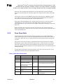
1
R
Mobile Intel Pentium III
Processor in BGA2 and MicroPGA2 Packages
Featuring Intel® SpeedStep™ Technology at
1 GHz, 900 MHz, 850 MHz, 800 MHz, 750 MHz,
700 MHz, Low-voltage 750MHz, Low-voltage
700MHz, Low-voltage 600 MHz, Ultra Lowvoltage 600 MHz and Ultra Low-voltage 500
MHz
Datasheet
Order Number: 283653-002
®
®
Mobile Intel Pentium III Processor in BGA2 and Micro-PGA2 Packages at 1 GHz,
900 MHz, 850 MHz, 800 MHz, 750 MHz, 700 MHz, Low-voltage 750 MHz, Low-voltage 700 MHz,
Low-voltage 600 MHz, Ultra Low-voltage 600 MHz and Ultra Low-voltage 500 MHz
Information in this document is provided in connection with Intel products. No license, express or implied, by estoppel or otherwise, to
any intellectual property rights is granted by this document. Except as provided in Intel's Terms and Conditions of Sale for such
products, Intel assumes no liability whatsoever, and Intel disclaims any express or implied warranty, relating to sale and/or use of Intel
products including liability or warranties relating to fitness for a particular purpose, merchantability, or infringement of any patent,
copyright or other intellectual property right. Intel products are not intended for use in medical, life saving, or life sustaining applications.
Intel may make changes to specifications and product descriptions at any time, without notice.
Designers must not rely on the absence or characteristics of any features or instructions marked "reserved" or "undefined." Intel
reserves these for future definition and shall have no responsibility whatsoever for conflicts or incompatibilities arising from future
changes to them.
The mobile Intel® Pentium® III processor may contain design defects or errors known as errata that may cause the product to deviate
from published specifications. Current characterized errata are available on request.
Contact your local Intel sales office or your distributor to obtain the latest specifications and before placing your product order.
Copies of documents which have an order number and are referenced in this document, or other Intel literature, may be obtained by
calling1-800-548-4725 or by visiting Intel’s web site at http://www.intel.com
Copyright © Intel Corporation, 1998-2001.
Intel®, Pentium® III, and SpeedStep™ Technology are trademarks or registered trademarks of Intel Corporation or its subsidiaries in
the United States and other countries.
* Other names and brands may be claimed as the property of others.
2
Datasheet
283653-002
®
®
Mobile Intel Pentium III Processor in BGA2 and Micro-PGA2 Packages at 1 GHz,
900 MHz, 850 MHz, 800 MHz, 750 MHz, 700 MHz, Low-voltage 750 MHz, Low-voltage
700 MHz, Low-voltage 600 MHz, Ultra Low-voltage 600 MHz and Ultra Low-voltage 500 MHz
Mobile Intel Pentium III
Processor in BGA2 and MicroPGA2 Packages
Product Features
!
Processor core/bus speeds:
Featuring Intel SpeedStep technology:
600/100 MHz ( Maximum Performance
Mode at 1.10V) and 300/100 MHz (Battery
Optimized Mode at 0.975V)
−
Featuring Intel SpeedStep technology:
500/100 MHz ( Maximum Performance
Mode at 1.10V) and 300/100 MHz (Battery
Optimized Mode at 0.975V)Supports the
Intel Architecture with Dynamic Execution
Featuring Intel® SpeedStepTM technology:
1000/100 MHz ( Maximum Performance Mode
at 1.70V) and 700/100 MHz (Battery Optimized
Mode at 1.35V)
−
Featuring Intel SpeedStep technology: 900/100
MHz ( Maximum Performance Mode at 1.70V)
and 700/100 MHz (Battery Optimized Mode at
1.35V)
−
!
Featuring Intel SpeedStep technology: 850/100
MHz ( Maximum Performance Mode at 1.60V)
and 700/100 MHz (Battery Optimized Mode at !
1.35V)
!
Featuring Intel SpeedStep technology: 800/100 !
MHz ( Maximum Performance Mode at 1.60V)
and 650/100 MHz (Battery Optimized Mode at !
1.35V)
!
On-die primary 16-Kbyte instruction cache and
16-Kbyte write-back data cache
Featuring Intel SpeedStep technology: 750/100
MHz ( Maximum Performance Mode at 1.60V)
and 600/100 MHz (Battery Optimized Mode at
1.35V)
− Supports thin form factor notebook designs
− Exposed die enables more efficient heat
−
−
−
Featuring Intel SpeedStep technology: 750/100
MHz ( Maximum Performance Mode at 1.35V) !
and 500/100 MHz (Battery Optimized Mode at
1.10V)
−
Featuring Intel SpeedStep technology: 700/100
MHz ( Maximum Performance Mode at 1.35V)
and 500/100 MHz (Battery Optimized Mode at
1.10V)
Integrated math co-processor
Intel Processor Serial Number
BGA2 and Micro-PGA2 packaging technologies
ULV=1.15V/ 0.975V) and Low Voltage
(LV=1.35V/ 1.10V) mobile Intel Pentium III
processors are only available in BGA2
packages.
Fully compatible with previous Intel
microprocessors
− Binary compatible with all applications
− Support for MMX™ technology
− Support for Streaming SIMD Extensions
!
Featuring Intel SpeedStep technology: 600/100
MHz ( Maximum Performance Mode at 1.35V)
and 500/100 MHz (Battery Optimized Mode at
1.10V)
!
Featuring Intel SpeedStep technology: 600/100
MHz ( Maximum Performance Mode at 1.150V)
and 300/100 MHz (Battery Optimized Mode at
0.975V)
Datasheet
Integrated GTL+ termination
dissipation
Featuring Intel SpeedStep technology: 700/100
MHz ( Maximum Performance Mode at 1.60V)
and 550/100 MHz (Battery Optimized Mode at
1.35V)
−
On-die second level cache (256-Kbyte)
− Ultra Low Voltage (ULV=1.10V/ 0.975V,
−
−
283653-002
−
−
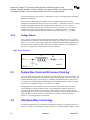
Power Management Features
− Quick Start and Deep Sleep modes provide
low power dissipation
On-die thermal diode
3
®
®
Mobile Intel Pentium III Processor in BGA2 and Micro-PGA2 Packages at 1 GHz,
900 MHz, 850 MHz, 800 MHz, 750 MHz, 700 MHz, Low-voltage 750 MHz, Low-voltage 700 MHz,
Low-voltage 600 MHz, Ultra Low-voltage 600 MHz and Ultra Low-voltage 500 MHz
Contents
1.
Introduction...................................................................................................................................10
1.1
1.2
1.3
2.
Mobile Pentium III Processor Features ......................................................................................15
2.1
2.2
2.3
2.4
3.
New Features in the Mobile Pentium III Processor ..............................................15
2.1.1 On-die GTL+ Termination .......................................................................15
2.1.2 Streaming SIMD Extensions ...................................................................15
2.1.3 Intel SpeedStep Technology ...................................................................15
2.1.4 Signal Differences Between the Mobile Pentium II Processor and the
Mobile Pentium III Processor...................................................................15
Power Management .............................................................................................16
2.2.1 Clock Control Architecture.......................................................................16
2.2.2 Normal State ...........................................................................................16
2.2.3 Auto Halt State ........................................................................................16
2.2.4 Stop Grant State......................................................................................17
2.2.5 Quick Start State .....................................................................................18
2.2.6 HALT/Grant Snoop State ........................................................................18
2.2.7 Sleep State ..............................................................................................18
2.2.8 Deep Sleep State ....................................................................................19
2.2.9 Operating System Implications of Low-power States .............................20
2.2.10 Intel SpeedStep Technology ...................................................................20
GTL+ Signals........................................................................................................20
Mobile Pentium III Processor CPUID ...................................................................20
Electrical Specifications ..............................................................................................................22
3.1
3.2
3.3
3.4
3.5
3.6
3.7
4
Overview...............................................................................................................13
Terminology..........................................................................................................13
References ...........................................................................................................14
Processor System Signals ...................................................................................22
3.1.1 Power Sequencing Requirements...........................................................23
3.1.2 Test Access Port (TAP) Connection .......................................................23
3.1.3 Catastrophic Thermal Protection.............................................................24
3.1.4 Unused Signals .......................................................................................24
3.1.5 Signal State in Low-power States ...........................................................24
3.1.5.1
System Bus Signals ..............................................................24
3.1.5.2
CMOS and Open-drain Signals.............................................25
3.1.5.3
Other Signals.........................................................................25
Power Supply Requirements................................................................................25
3.2.1 Decoupling Recommendations ...............................................................25
3.2.2 Voltage Planes ........................................................................................26
System Bus Clock and Processor Clocking .........................................................26
Intel SpeedStep Technology ................................................................................26
Maximum Ratings.................................................................................................27
DC Specifications .................................................................................................28
AC Specifications .................................................................................................32
Datasheet
283653-002
®
®
Mobile Intel Pentium III Processor in BGA2 and Micro-PGA2 Packages at 1 GHz,
900 MHz, 850 MHz, 800 MHz, 750 MHz, 700 MHz, Low-voltage 750 MHz, Low-voltage
700 MHz, Low-voltage 600 MHz, Ultra Low-voltage 600 MHz and Ultra Low-voltage 500 MHz
3.7.1
4.
System Signal Simulations .........................................................................................................44
4.1
4.2
4.3
5.
Thermal Diode ......................................................................................................65
Processor Initialization and Configuration................................................................................66
7.1
7.2
8.
Surface-mount BGA2 Package Dimensions ........................................................49
Socketable Micro-PGA2 Package Dimensions ....................................................52
Signal Listings ......................................................................................................54
Thermal Specifications ................................................................................................................63
6.1
7.
System Bus Clock (BCLK) and PICCLK AC Signal Quality Specifications .........44
GTL+ AC Signal Quality Specifications................................................................45
Non-GTL+ Signal Quality Specifications ..............................................................47
4.3.1 PWRGOOD Signal Quality Specifications ..............................................48
Mechanical Specifications...........................................................................................................49
5.1
5.2
5.3
6.
System Bus, Clock, APIC, TAP, CMOS, and Open-drain AC
Specifications ..........................................................................................32
Description............................................................................................................66
7.1.1 Quick Start Enable ..................................................................................66
7.1.2 System Bus Frequency ...........................................................................66
7.1.3 APIC Enable ............................................................................................66
Clock Frequencies and Ratios .............................................................................66
Processor Interface ......................................................................................................................67
8.1
8.2
Alphabetical Signal Reference .............................................................................67
Signal Summaries ................................................................................................80
Appendix A: PLL RLC Filter Specification..............................................................................................82
A.1
A.2
A.3
A.4
Introduction...........................................................................................................82
Filter Specification ................................................................................................82
Recommendation for Mobile Systems .................................................................84
Comments ............................................................................................................85
Appendix B: Intel Mobile Voltage Positioning (IMVP) for the Mobile Pentium III Processor.............86
B.1
B.2
283653-002
Introduction...........................................................................................................86
Reference Documents..........................................................................................86
Datasheet
5
®
®
Mobile Intel Pentium III Processor in BGA2 and Micro-PGA2 Packages at 1 GHz,
900 MHz, 850 MHz, 800 MHz, 750 MHz, 700 MHz, Low-voltage 750 MHz, Low-voltage 700 MHz,
Low-voltage 600 MHz, Ultra Low-voltage 600 MHz and Ultra Low-voltage 500 MHz
Figures
Figure 1. Signal Groups of a Mobile Pentium III Processor/440BX AGPset - Based
System ..............................................................................................................11
Figure 2. Signal Groups of a Mobile Pentium III Processor/440MX Chipset - Based
System ..............................................................................................................12
Figure 3. Clock Control States ..........................................................................................17
Figure 4. Vcc Ramp Rate Requirement ............................................................................23
Figure 5. PLL RLC Filter....................................................................................................26
Figure 6. PICCLK/TCK Clock Timing Waveform...............................................................38
Figure 7. BCLK Timing Waveform.....................................................................................38
Figure 8. Valid Delay Timings ...........................................................................................39
Figure 9. Setup and Hold Timings.....................................................................................39
Figure 10. Cold/Warm Reset and Configuration Timings..................................................40
Figure 11. Power-on Reset Timings..................................................................................40
Figure 12. Test Timings (Boundary Scan) ........................................................................41
Figure 13. Test Reset Timings ..........................................................................................42
Figure 14. Quick Start/Deep Sleep Timing........................................................................42
Figure 15. Stop Grant/Sleep/Deep Sleep Timing..............................................................43
Figure 16. Intel SpeedStep Technology/Deep Sleep Timing ............................................43
Figure 17. BCLK/PICCLK Generic Clock Waveform.........................................................45
Figure 18. Low to High, GTL+ Receiver Ringback Tolerance...........................................46
Figure 19. High to Low, GTL+ Receiver Ringback Tolerance...........................................46
Figure 20. Maximum Acceptable Overshoot/Undershoot Waveform................................47
Figure 21. Surface-mount BGA2 Package - Top and Side View ......................................50
Figure 22. Surface-mount BGA2 Package - Bottom View ................................................51
Figure 23. Socketable Micro-PGA2 Package - Top and Side View ..................................53
Figure 24. Socketable Micro-PGA2 Package - Bottom View ............................................54
Figure 25. Pin/Ball Map - Top View...................................................................................55
Figure 26. PWRGOOD Relationship at Power On............................................................74
Figure 27. PLL Filter Specifications ..................................................................................83
6
Datasheet
283653-002
®
®
Mobile Intel Pentium III Processor in BGA2 and Micro-PGA2 Packages at 1 GHz,
900 MHz, 850 MHz, 800 MHz, 750 MHz, 700 MHz, Low-voltage 750 MHz, Low-voltage
700 MHz, Low-voltage 600 MHz, Ultra Low-voltage 600 MHz and Ultra Low-voltage 500 MHz
Tables
Table 1. New Mobile Pentium III Processor Signals .........................................................15
Table 2. Removed Mobile Pentium II Processor Signals ..................................................16
Table 3. Clock State Characteristics .................................................................................19
Table 4. Mobile Pentium III Processor CPUID ..................................................................21
Table 5. Mobile Pentium III Processor CPUID Cache and TLB Descriptors.....................21
Table 6. System Signal Groups.........................................................................................22
Table 7. Recommended Resistors for Mobile Pentium III Processor Signals ..................23
Table 8. Mobile Pentium III Processor Absolute Maximum Ratings .................................27
Table 9A. Mobile Pentium III Processor DC Specifications ..............................................29
Table 9B. Mobile Pentium III Processor DC Specifications ..............................................29
Table 10. GTL+ Signal Group DC Specifications..............................................................30
Table 11. GTL+ Bus DC Specifications.............................................................................30
Table 12. Clock, APIC, TAP, CMOS, and Open-drain Signal Group DC Specifications ..31
Table 13. System Bus Clock AC Specifications................................................................32
Table 14. Valid Mobile Pentium III Processor Frequencies...............................................33
Table 15. GTL+ Signal Groups AC Specifications ............................................................33
Table 16. CMOS and Open-drain Signal Groups AC Specifications ................................34
Table 17. Reset Configuration AC Specifications .............................................................34
Table 18. APIC Bus Signal AC Specifications ..................................................................35
Table 19. TAP Signal AC Specifications ...........................................................................36
Table 20. Quick Start/Deep Sleep AC Specifications .......................................................36
Table 21. Stop Grant/Sleep/Deep Sleep AC Specifications .............................................37
Table 22. Intel SpeedStep Technology AC Specifications................................................37
Table 23. BCLK Signal Quality Specifications ..................................................................44
Table 24. PICCLK Signal Quality Specifications...............................................................44
Table 25. GTL+ Signal Group Ringback Specification......................................................45
Table 26. GTL+ Signal Group Overshoot/Undershoot Tolerance at the Processor Core.47
Table 27. Non-GTL+ Signal Group Overshoot/Undershoot Tolerance at the Processor
Core .................................................................................................................48
Table 28. Surface-mount BGA2 Package Specifications..................................................49
Table 29. Socketable Micro-PGA2 Package Specification ...............................................52
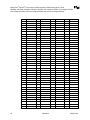
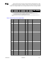
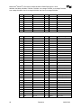
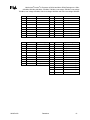
Table 30. Signal Listing in Order by Pin/Ball Number .......................................................56
Table 31. Signal Listing in Order by Signal Name ............................................................59
Table 32. Voltage and No-Connect Pin/Ball Locations .....................................................62
Table 33. Power Specifications for Mobile Pentium III Processor with Intel SpeedStep
Technology........................................................................................................64
Table 34. Thermal Diode Interface....................................................................................65
Table 35. Thermal Diode Specifications ...........................................................................65
Table 36. BSEL[1:0] Encoding ..........................................................................................70
Table 37. Voltage Identification Encoding.........................................................................79
Table 38. Input Signals......................................................................................................80
Table 39. Output Signals...................................................................................................80
Table 40. Input/Output Signals (Single Driver)..................................................................81
Table 41. Input/Output Signals (Multiple Driver) ...............................................................81
Table 42. PLL Filter Inductor Recommendations..............................................................84
Table 43. PLL Filter Capacitor Recommendations ...........................................................84
Table 44. PLL Filter Resistor Recommendations..............................................................84
283653-002
Datasheet
7
®
®
Mobile Intel Pentium III Processor in BGA2 and Micro-PGA2 Packages at 1 GHz,
900 MHz, 850 MHz, 800 MHz, 750 MHz, 700 MHz, Low-voltage 750 MHz, Low-voltage 700 MHz,
Low-voltage 600 MHz, Ultra Low-voltage 600 MHz and Ultra Low-voltage 500 MHz
Revision History
Date
Revision
Number
Updates
April 2000
1.0
Initial release
June 2000
2.0
Revision 2.0 updates include:
September 2000
January 2001
February 2001
March 2001
May 2001
July 2001
3.0
4.0
5.0
6.0
283653-001
283653-002
•
Added new processor speed 750/600 MHz
•
Added new Low Voltage processor speed 600/500 MHz
•
Updated references
Revision 3.0 updates include:
•
Added new processor speed 850/700 MHz, 800/650 MHz
•
Updated references
Revision 4.0 updates include:
•
Added new Ultra Low Voltage processor speed 500/300 MHz
•
Updated references
•
Corrected die width size for C-step in Table 28
•
Updated the decoupling recommendations in Section 3.2.1
•
Updated the Pin/Ball P1 connection guideline in Section 5.3
Revision 5.0 updates include:
•
Added new Low Voltage processor speed 700/500 MHz
•
Updated references
•
Updated current specifications in Table 9 and power specifications
in Table 33
Revision 6.0 updates include:
•
Added new processor speed 900/700 MHz and 1GHz/700 MHz
•
Updated references
•
Updated current specifications in Table 9 and power specifications
in Table 33
•
Updated die width and length size in Table 28
•
Updated die width and length size in Table 29
Revision 7.0 updates include:
•
Added new Low Voltage 750/500 MHz and Ultra Low Voltage
600/300 MHz processor speeds
•
Added new 1GHz/700 MHz at Tj=92°C power specification in
Table 33
•
Reformatted Table 9 to Table 9A and Table 9B. Table 9B shows
battery optimized mode current specifications.
•
Updated references
•
Updated current specifications in Table 9B and power specifications
in Table 33
Revision 8.0 updates include:
•
8
Added new Ultra Low Voltage 600/300 MHz (1.15V/ 0.975V )
processor speed
Datasheet
283653-002
®
®
Mobile Intel Pentium III Processor in BGA2 and Micro-PGA2 Packages at 1 GHz,
900 MHz, 850 MHz, 800 MHz, 750 MHz, 700 MHz, Low-voltage 750 MHz, Low-voltage
700 MHz, Low-voltage 600 MHz, Ultra Low-voltage 600 MHz and Ultra Low-voltage 500 MHz
processor speed
283653-002
•
Updated references in Table 9A, 9B and power specifications in
Table 33
•
Documentation Change to replace four TESTP (Test Point) signal
to NC (No Connect) in Section 5 and 8
Datasheet
9
®
®
Mobile Intel Pentium III Processor in BGA2 and Micro-PGA2 Packages at 1 GHz,
900 MHz, 850 MHz, 800 MHz, 750 MHz, 700 MHz, Low-voltage 750 MHz, Low-voltage 700 MHz,
Low-voltage 600 MHz, Ultra Low-voltage 600 MHz and Ultra Low-voltage 500 MHz
1.
Introduction
Using Intel’s advanced 0.18 micron process technology, the mobile Intel® Pentium® III processor
offers high performance and lower power consumption. Key Performance advancements include
the addition of new Internet Streaming SIMD instructions, an advanced transfer cache
architecture, and a processor system bus speed of 100 MHz. These features are offered in BGA2
and micro-PGA2 packages that are up to 20% smaller than those offered for the mobile Intel
Pentium II processor. All of these technologies make outstanding performance possible for
mobile PCs in a variety of shapes and sizes.
The mobile Intel Pentium III processor featuring Intel SpeedStep™ technology is the next dramatic
step towards achieving near desktop performance. This exciting new processor has two
performance modes and allows real-time dynamic switching of the voltage and frequency between
the modes. This occurs by switching the bus ratios, core operating voltage, and core processor
speeds without resetting the system.
The integrated L2 cache is designed to help improve performance, and it complements the system
bus by providing critical data faster and reducing total system power consumption. The mobile
Pentium III processor’s 64-bit wide Gunning Transceiver Logic (GTL+) system bus provides a
glue-less, point-to-point interface for an I/O bridge/memory controller, and is compatible with the
440BX AGPset, 815EM, 440ZX-M AGPset, and the 440MX Chipset.
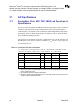
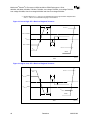
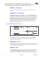
Figure 1 shows the various parts of a mobile Pentium III processor/440BX or 440ZX-M AGPset –
based system and how the mobile Pentium III processor connects to them.
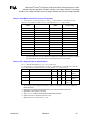
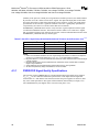
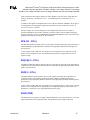
Figure 2 shows an alternative mobile Pentium III processor/440MX Chipset - based system.
This document covers the electrical, mechanical, and thermal specifications for the mobile
Pentium III processor featuring Intel SpeedStep technology at the following frequencies: 1 GHz,
900 MHz, 850 MHz, 800 MHz, 750 MHz and 700 MHz in BGA2 and micro-PGA2 packages,
low voltage 750 MHz, low voltage 700 MHz, low voltage 600 MHz, ultra low voltage 600 MHz,
and ultra low voltage 500 MHz in BGA2 packages.
10
Datasheet
283653-002
®
®
Mobile Intel Pentium III Processor in BGA2 and Micro-PGA2 Packages at 1 GHz,
900 MHz, 850 MHz, 800 MHz, 750 MHz, 700 MHz, Low-voltage 750 MHz, Low-voltage
700 MHz, Low-voltage 600 MHz, Ultra Low-voltage 600 MHz and Ultra Low-voltage 500 MHz
Figure 1. Signal Groups of a Mobile Pentium III Processor/440BX AGPset - Based System
Thermal
Sensor
Mobile
Pentium® III
Processor
APIC
Bus
TAP
System
SMBus
Bus
Open Drain
CMOS/
443BX
OR
440ZX-M
North Bridge
OR
System
Controller
PCI
PIIX4E
South Bridge
IOAPIC
(optional)
ISA/EIO
283653-002
DRAM
Datasheet
V0000-03
11
®
®
Mobile Intel Pentium III Processor in BGA2 and Micro-PGA2 Packages at 1 GHz,
900 MHz, 850 MHz, 800 MHz, 750 MHz, 700 MHz, Low-voltage 750 MHz, Low-voltage 700 MHz,
Low-voltage 600 MHz, Ultra Low-voltage 600 MHz and Ultra Low-voltage 500 MHz
Figure 2. Signal Groups of a Mobile Pentium III Processor/440MX Chipset - Based System
Thermal
Sensor
Mobile
®
Pentium III
Processor
TAP
Open Drain
CMOS/
SMBus
System
Bus
DRAM
440MX
PCIset
OR
System
Controller
V0000-04
X-bus
12
PCI
Datasheet
283653-002
®
®
Mobile Intel Pentium III Processor in BGA2 and Micro-PGA2 Packages at 1 GHz,
900 MHz, 850 MHz, 800 MHz, 750 MHz, 700 MHz, Low-voltage 750 MHz, Low-voltage
700 MHz, Low-voltage 600 MHz, Ultra Low-voltage 600 MHz and Ultra Low-voltage 500 MHz
1.1
Overview
Performance improved over existing mobile processors
— Supports the Intel Architecture with Dynamic Execution
— Supports the Intel Architecture MMX™ technology
— Supports Streaming SIMD Extensions for enhanced video, sound, and 3D performance
— Supports Intel SpeedStep Technology
— Integrated Intel Floating Point Unit compatible with the IEEE 754 standard
On-die primary (L1) instruction and data caches
— 4-way set associative, 32-byte line size, 1 line per sector
— 16-Kbyte instruction cache and 16-Kbyte write-back data cache
— Cacheable range controlled by processor programmable registers
On-die second level (L2) cache
— 8-way set associative, 32-byte line size, 1 line per sector
— Operates at full core speed
— 256-Kbyte, ECC protected cache data array
GTL+ system bus interface
— 64-bit data bus, 100-MHz operation
— Uniprocessor, two loads only (processor and I/O bridge/memory controller)
— Integrated termination
Pentium II processor clock control
— Quick Start for low power, low exit latency clock “throttling”
— Deep Sleep mode for lower power dissipation
Thermal diode for measuring processor temperature
1.2
Terminology
In this document a “#” symbol following a signal name indicates that the signal is active low. This
means that when the signal is asserted (based on the name of the signal) it is in an electrical low
state. Otherwise, signals are driven in an electrical high state when they are asserted. In state
machine diagrams, a signal name in a condition indicates the condition of that signal being
asserted. If the signal name is preceded by a “!” symbol, then it indicates the condition of that
signal not being asserted. For example, the condition “!STPCLK# and HS” is equivalent to “the
active low signal STPCLK# is unasserted (i.e., it is at 1.5V) and the HS condition is true.” The
symbols “L” and “H” refer respectively to electrical low and electrical high signal levels. The
283653-002
Datasheet
13
®
®
Mobile Intel Pentium III Processor in BGA2 and Micro-PGA2 Packages at 1 GHz,
900 MHz, 850 MHz, 800 MHz, 750 MHz, 700 MHz, Low-voltage 750 MHz, Low-voltage 700 MHz,
Low-voltage 600 MHz, Ultra Low-voltage 600 MHz and Ultra Low-voltage 500 MHz
symbols “0” and “1” refer respectively to logical low and logical high signal levels. For example,
BD[3:0] = “1010” = “HLHL” refers to a hexadecimal “A,” and D[3:0]# = “1010” = “LHLH” also
refers to a hexadecimal “A.” The symbol “X” refers to a “Don’t Care” condition, where a “0” or a
“1” results in the same behavior.
1.3
References
• Pentium® III Processor at 1 GHz, 900 MHz, 850 MHz, 800 MHz, 750 MHz, 700 MHz, Lowvoltage 750 MHz, Low voltage 700 MHz, Low-voltage 600 MHz, Ultra Low-voltage 600 MHz
and Ultra Low-voltage 500 MHz Datasheet (Order Number 283653-001)
• Mobile Pentium® III Processor I/O Buffer Models, IBIS Format (Available in electronic form;
Contact your Intel Field Sales Representative)
• Mobile Pentium® III Processor GTL+ System Bus Layout Guideline (Contact your Intel Field
Sales Representative)
• Mobile Pentium® II Processor in Micro-PGA and BGA Packages at 400 MHz, 366 MHz, 333
MHz, 300 PE MHz and 266 PE MHz Datasheet (Order Number 245103-003)
• Mobile Pentium® II Processor in Mini Cartridge at 400 MHz, 366 MHz, 333 MHz, 300 PE
MHz and 266 PE MHz Datasheet (Order Number 245108-002)
• P6 Family of Processors Hardware Developer’s Manual (Order Number 244001-001)
• CK97 Clock Driver Specification (Contact your Intel Field Sales Representative)
• Intel® Architecture Optimization Manual (Order Number 242816-003)
• Intel® Architecture Software Developer’s Manual Volume I: Basic Architecture (Order Number
243190)
• Intel® Architecture Software Developer’s Manual Volume II: Instruction Set Reference (Order
Number 243191)
• Intel® Architecture Software Developer’s Manual Volume III: System Programming Guide
(Order Number 243192)
14
Datasheet
283653-002
®
®
Mobile Intel Pentium III Processor in BGA2 and Micro-PGA2 Packages at 1 GHz,
900 MHz, 850 MHz, 800 MHz, 750 MHz, 700 MHz, Low-voltage 750 MHz, Low-voltage
700 MHz, Low-voltage 600 MHz, Ultra Low-voltage 600 MHz and Ultra Low-voltage 500 MHz
2.
Mobile Pentium III Processor
Features
2.1
New Features in the Mobile Pentium III Processor
2.1.1
On-die GTL+ Termination
The termination resistors for the GTL+ system bus are integrated onto the processor die. The
RESET# signal does not have on-die termination and requires an external 56.2Ω ±1% terminating
resistor.
2.1.2
Streaming SIMD Extensions
The mobile Pentium III processor is the first mobile processor to implement Streaming SIMD
(single instruction, multiple data) extensions. Streaming SIMD extensions can enhance floating
point, video, sound, and 3-D application performance.
2.1.3
Intel SpeedStep Technology
Intel SpeedStep technology is a new mobile feature developed by Intel. The mobile Pentium III
processors that are enabled with Intel SpeedStep technology have the ability to switch between
two bus ratios and core speeds without having to reset the processor.
2.1.4
Signal Differences Between the Mobile Pentium II
Processor and the Mobile Pentium III Processor
With the exception of BCLK, PICCLK, and PWRGOOD, the CMOS inputs and Open-drain
outputs have changed from 2.5V tolerant, as on the mobile Pentium II processor to 1.5V tolerant.
Table 1. New Mobile Pentium III Processor Signals
Signals
283653-002
Function
CLKREF
System bus clock trip point control
CMOSREF
1.5V CMOS input buffer trip point control
EDGECTRLP
GTL+ output buffer control
GHI#
Intel SpeedStep technology operating mode selection
BSEL[1:0]
Processor system bus speed selection
RSVD
Reserved, may be defined in the future
RTTIMPEDP
On-die GTL+ termination control
VCCT
On-die GTL+ termination current supply
VID[4:0]
Voltage Identification
Datasheet
15
®
®
Mobile Intel Pentium III Processor in BGA2 and Micro-PGA2 Packages at 1 GHz,
900 MHz, 850 MHz, 800 MHz, 750 MHz, 700 MHz, Low-voltage 750 MHz, Low-voltage 700 MHz,
Low-voltage 600 MHz, Ultra Low-voltage 600 MHz and Ultra Low-voltage 500 MHz
Table 2. Removed Mobile Pentium II Processor Signals
Signals
Purpose
EDGECTRLN
GTL+ output buffer control
BSEL
100/66 MHz processor system bus speed selection
2.2
Power Management
2.2.1
Clock Control Architecture
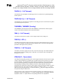
The mobile Pentium III processor clock control architecture (Figure 3) has been optimized for
leading edge deep green desktop and mobile computer designs. The clock control architecture
consists of seven different clock states: Normal, Stop Grant, Auto Halt, Quick Start, HALT/Grant
Snoop, Sleep, and Deep Sleep states. The Auto Halt state provides a low-power clock state that
can be controlled through the software execution of the HLT instruction. The Quick Start state
provides a very low power and low exit latency clock state that can be used for hardware
controlled “idle” computer states. The Deep Sleep state provides an extremely low-power state
that can be used for “Power-On-Suspend” computer states, which is an alternative to shutting off
the processor’s power. Compared to the Pentium processor exit latency of 1 msec, the exit latency
of the Deep Sleep state has been reduced to 30 µsec in the mobile Pentium III processor. The Stop
Grant and Sleep states shown in Figure 3 are intended for use in “Deep Green” desktop and server
systems — not in mobile systems. Performing state transitions not shown in Figure 3 is neither
recommended nor supported.
The Stop Grant and Quick Start clock states are mutually exclusive, i.e., a strapping option on
signal A15# chooses which state is entered when the STPCLK# signal is asserted. The Quick Start
state is enabled by strapping the A15# signal to ground at Reset; otherwise, asserting the
STPCLK# signal puts the processor into the Stop Grant state. The Stop Grant state has a higher
power level than the Quick Start state and is designed for Symmetric Multi-Processing (SMP)
platforms. The Quick Start state has a much lower power level, but it can only be used in
uniprocessor platforms. Table 3 provides clock state characteristics, which are described in detail
in the following sections.
2.2.2
Normal State
The Normal state of the processor is the normal operating mode where the processor’s core clock
is running and the processor is actively executing instructions.
2.2.3
Auto Halt State
This is a low-power mode entered by the processor through the execution of the HLT instruction.
The power level of this mode is similar to the Stop Grant state. A transition to the Normal state is
made by a halt break event (one of the following signals going active: NMI, INTR, BINIT#,
INIT#, RESET#, FLUSH#, or SMI#).
Asserting the STPCLK# signal while in the Auto Halt state will cause the processor to transition
to the Stop Grant or Quick Start state, where a Stop Grant Acknowledge bus cycle will be issued.
Deasserting STPCLK# will cause the processor to return to the Auto Halt state without issuing a
new Halt bus cycle.
16
Datasheet
283653-002
®
®
Mobile Intel Pentium III Processor in BGA2 and Micro-PGA2 Packages at 1 GHz,
900 MHz, 850 MHz, 800 MHz, 750 MHz, 700 MHz, Low-voltage 750 MHz, Low-voltage
700 MHz, Low-voltage 600 MHz, Ultra Low-voltage 600 MHz and Ultra Low-voltage 500 MHz
The SMI# interrupt is recognized in the Auto Halt state. The return from the System Management
Interrupt (SMI) handler can be to either the Normal state or the Auto Halt state. See the Intel®
Architecture Software Developer’s Manual, Volume III: System Programmer’s Guide for more
information. No Halt bus cycle is issued when returning to the Auto Halt state from the System
Management Mode (SMM).
The FLUSH# signal is serviced in the Auto Halt state. After the on-chip and off-chip caches have
been flushed, the processor will return to the Auto Halt state without issuing a Halt bus cycle.
Transitions in the A20M# and PREQ# signals are recognized while in the Auto Halt state.
Figure 3. Clock Control States
STPCLK# and
QSE and SGA
Normal
HS=false
Quick
Start
(!STPCLK# and !HS)
or RESET#
HLT and
halt bus cycle
STPCLK# and
QSE and SGA
halt
break
BCLK
stopped
!STPCLK#
and HS
STPCLK# and
!QSE and SGA
(!STPCLK#
and !HS) or
stop break !STPCLK#
and HS
Auto
Halt
HS=true
Snoop
serviced
BCLK on
and QSE
Deep
Sleep
Snoop
occurs
Snoop
occurs
STPCLK# and
!QSE and SGA
Snoop
occurs
Snoop
serviced
Stop
Grant
HALT/Grant
Snoop
Snoop
serviced
SLP#
BCLK
stopped
!SLP# or
RESET#
BCLK on
and !QSE
Sleep
V0001-00
NOTES:
2.2.4
halt break – A20M#, BINIT#, FLUSH#, INIT#, INTR, NMI, PREQ#, RESET#, SMI#
HLT – HLT instruction executed
HS – Processor Halt State
QSE – Quick Start State Enabled
SGA – Stop Grant Acknowledge bus cycle issued
stop break – BINIT#, RESET#
Stop Grant State
The processor enters this mode with the assertion of the STPCLK# signal when it is configured for
Stop Grant state (via the A15# strapping option). The processor is still able to respond to snoop
requests and latch interrupts. Latched interrupts will be serviced when the processor returns to the
Normal state. Only one occurrence of each interrupt event will be latched. A transition back to the
283653-002
Datasheet
17
®
®
Mobile Intel Pentium III Processor in BGA2 and Micro-PGA2 Packages at 1 GHz,
900 MHz, 850 MHz, 800 MHz, 750 MHz, 700 MHz, Low-voltage 750 MHz, Low-voltage 700 MHz,
Low-voltage 600 MHz, Ultra Low-voltage 600 MHz and Ultra Low-voltage 500 MHz
Normal state can be made by the deassertion of the STPCLK# signal or the occurrence of a stop
break event (a BINIT# or RESET# assertion).
The processor will return to the Stop Grant state after the completion of a BINIT# bus
initialization unless STPCLK# has been de-asserted. RESET# assertion will cause the processor to
immediately initialize itself, but the processor will stay in the Stop Grant state after initialization
until STPCLK# is deasserted. A transition to the Sleep state can be made by the assertion of the
SLP# signal.
While in the Stop Grant state, assertions of FLUSH#, SMI#, INIT#, INTR, and NMI (or
LINT[1:0]) will be latched by the processor. These latched events will not be serviced until the
processor returns to the Normal state. Only one of each event will be recognized upon return to the
Normal state.
2.2.5
Quick Start State
This is a mode entered by the processor with the assertion of the STPCLK# signal when it is
configured for the Quick Start state (via the A15# strapping option). In the Quick Start state the
processor is only capable of acting on snoop transactions generated by the system bus priority
device. Because of its snooping behavior, Quick Start can only be used in a uniprocessor (UP)
configuration.
A transition to the Deep Sleep state can be made by stopping the clock input to the processor. A
transition back to the Normal state (from the Quick Start state) is made only if the STPCLK#
signal is deasserted.
While in this state the processor is limited in its ability to respond to input. It is incapable of
latching any interrupts, servicing snoop transactions from symmetric bus masters or responding to
FLUSH# or BINIT# assertions. While the processor is in the Quick Start state, it will not respond
properly to any input signal other than STPCLK#, RESET#, or BPRI#. If any other input signal
changes, then the behavior of the processor will be unpredictable. No serial interrupt messages
may begin or be in progress while the processor is in the Quick Start state.
RESET# assertion will cause the processor to immediately initialize itself, but the processor will
stay in the Quick Start state after initialization until STPCLK# is deasserted.
2.2.6
HALT/Grant Snoop State
The processor will respond to snoop transactions on the system bus while in the Auto Halt, Stop
Grant, or Quick Start state. When a snoop transaction is presented on the system bus the processor
will enter the HALT/Grant Snoop state. The processor will remain in this state until the snoop has
been serviced and the system bus is quiet. After the snoop has been serviced, the processor will
return to its previous state. If the HALT/Grant Snoop state is entered from the Quick Start state,
then the input signal restrictions of the Quick Start state still apply in the HALT/Grant Snoop
state, except for those signal transitions that are required to perform the snoop.
2.2.7
Sleep State
The Sleep state is a very low-power state in which the processor maintains its context and the
phase-locked loop (PLL) maintains phase lock. The Sleep state can only be entered from the Stop
18
Datasheet
283653-002
®
®
Mobile Intel Pentium III Processor in BGA2 and Micro-PGA2 Packages at 1 GHz,
900 MHz, 850 MHz, 800 MHz, 750 MHz, 700 MHz, Low-voltage 750 MHz, Low-voltage
700 MHz, Low-voltage 600 MHz, Ultra Low-voltage 600 MHz and Ultra Low-voltage 500 MHz
Grant state. After entering the Stop Grant state, the SLP# signal can be asserted, causing the
processor to enter the Sleep state. The SLP# signal is not recognized in the Normal or Auto Halt
states.
The processor can be reset by the RESET# signal while in the Sleep state. If RESET# is driven
active while the processor is in the Sleep state then SLP# and STPCLK# must immediately be
driven inactive to ensure that the processor correctly initializes itself.
Input signals (other than RESET#) may not change while the processor is in the Sleep state or
transitioning into or out of the Sleep state. Input signal changes at these times will cause
unpredictable behavior. Thus, the processor is incapable of snooping or latching any events in the
Sleep state.
While in the Sleep state, the processor can enter its lowest power state, the Deep Sleep state.
Removing the processor’s input clock puts the processor in the Deep Sleep state. PICCLK may be
removed in the Sleep state.
2.2.8
Deep Sleep State
The Deep Sleep state is the lowest power mode the processor can enter while maintaining its
context. The Deep Sleep state is entered by stopping the BCLK input to the processor, while it is
in the Sleep or Quick Start state. For proper operation, the BCLK input should be stopped in the
Low state.
The processor will return to the Sleep or Quick Start state from the Deep Sleep state when the
BCLK input is restarted. Due to the PLL lock latency, there is a delay of up to 30 µsec after the
clocks have started before this state transition happens. PICCLK may be removed in the Deep
Sleep state. PICCLK should be designed to turn on when BCLK turns on when transitioning out of
the Deep Sleep state.
The input signal restrictions for the Deep Sleep state are the same as for the Sleep state, except
that RESET# assertion will result in unpredictable behavior.
Table 3. Clock State Characteristics
Clock State
Exit Latency
Snooping?
System Uses
Normal
N/A
Yes
Normal program execution
Auto Halt
Approximately 10 bus clocks
Yes
S/W controlled entry idle mode
Stop Grant
10 bus clocks
Yes
H/W controlled entry/exit mobile throttling
Quick Start
Through snoop, to HALT/Grant
Snoop state: immediate
Yes
H/W controlled entry/exit mobile throttling
Through STPCLK#, to Normal
state: 8 bus clocks
HALT/Grant
Snoop
A few bus clocks after the end
of snoop activity
Yes
Supports snooping in the low power states
Sleep
To Stop Grant state 10 bus
clocks
No
H/W controlled entry/exit desktop idle mode
support
Deep Sleep
30 µsec
No
H/W controlled entry/exit mobile powered-on
suspend support
NOTE:
283653-002
See Table 33 for power dissipation in the low-power states.
Datasheet
19
®
®
Mobile Intel Pentium III Processor in BGA2 and Micro-PGA2 Packages at 1 GHz,
900 MHz, 850 MHz, 800 MHz, 750 MHz, 700 MHz, Low-voltage 750 MHz, Low-voltage 700 MHz,
Low-voltage 600 MHz, Ultra Low-voltage 600 MHz and Ultra Low-voltage 500 MHz
2.2.9
Operating System Implications of Low-power States
There are a number of architectural features of the mobile Pentium III processor that do not
function in the Quick Start or Sleep state as they do in the Stop Grant state. The time-stamp
counter and the performance monitor counters are not guaranteed to count in the Quick Start or
Sleep states. The local APIC timer and performance monitor counter interrupts should be disabled
before entering the Deep Sleep state or the resulting behavior will be unpredictable.
2.2.10
Intel SpeedStep Technology
Some mobile Pentium III processors will be offered with Intel SpeedStep technology. The Intel
SpeedStep technology allows the processor switch between two core frequencies without having
to reset the processor or change the system bus frequency. The processor has two bus ratios
programmed into it instead of one and the GHI# signal controls which one is used. After reset, the
processor will start in the lower of its two core frequencies, the “Battery Optimized” mode. An
operating mode transition to the high core frequency can be made by putting the processor into the
Deep Sleep state, raising the core voltage, setting GHI# low, and returning to the Normal state.
This puts the processor into the “Maximum performance” mode. A transitioning back to the lowcore frequency can be made by reversing these steps.
2.3
GTL+ Signals
The mobile Pentium III processor system bus signals use a variation of the low-voltage swing GTL
signaling technology. The mobile Pentium III processor system bus specification is similar to the
Pentium II processor system bus specification, which is a version of GTL with enhanced noise
margins and less ringing.
The GTL+ system bus depends on incident wave switching and uses flight time for timing
calculations of the GTL+ signals, as opposed to capacitive derating. Analog signal simulation of
the system bus including trace lengths is highly recommended. Contact your field sales
representative to receive the IBIS models for the mobile Pentium III processor.
The GTL+ system bus of the Pentium II processor was designed to support high-speed data
transfers with multiple loads on a long bus that behaves like a transmission line. However, in
mobile systems the system bus only has two loads (the processor and the chipset) and the bus
traces are short. It is possible to change the layout and termination of the system bus to take
advantage of the mobile environment using the same GTL+ I/O buffers. In mobile systems the
GTL+ system bus is terminated at one end only. This termination is provided on the processor
core (except for the RESET# signal). Refer to the Mobile Pentium® III Processor GTL+ System
Bus Layout Guideline for details on laying out the GTL+ system bus.
2.4
Mobile Pentium III Processor CPUID
The CPUID instruction does not distinguish between the Pentium III processor and the mobile
Pentium III processor. After a power-on RESET or when the CPUID version information is
loaded, the EAX register contains the values shown in
Table 4. After the L2 cache is initialized, the CPUID cache/TLB descriptors will be the values
shown in Table 5.
20
Datasheet
283653-002
®
®
Mobile Intel Pentium III Processor in BGA2 and Micro-PGA2 Packages at 1 GHz,
900 MHz, 850 MHz, 800 MHz, 750 MHz, 700 MHz, Low-voltage 750 MHz, Low-voltage
700 MHz, Low-voltage 600 MHz, Ultra Low-voltage 600 MHz and Ultra Low-voltage 500 MHz
Table 4. Mobile Pentium III Processor CPUID
EAX[31:0]
EBX[7:0]
Reserved [31:14] Type [13:12] Family [11:8]
Model [7:4] Stepping [3:0]
Brand ID
X
8
02
0
6
X
Table 5. Mobile Pentium III Processor CPUID Cache and TLB Descriptors
Cache and TLB Descriptors
283653-002
01H, 02H, 03H, 04H, 08H, 0CH, 82H
Datasheet
21
®
®
Mobile Intel Pentium III Processor in BGA2 and Micro-PGA2 Packages at 1 GHz,
900 MHz, 850 MHz, 800 MHz, 750 MHz, 700 MHz, Low-voltage 750 MHz, Low-voltage 700 MHz,
Low-voltage 600 MHz, Ultra Low-voltage 600 MHz and Ultra Low-voltage 500 MHz
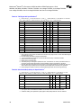
3.
Electrical Specifications
3.1
Processor System Signals
Table 6 lists the processor system signals by type. All GTL+ signals are synchronous with the
BCLK signal. All TAP signals are synchronous with the TCK signal except TRST#. All CMOS
input signals can be applied asynchronously.
Table 6. System Signal Groups
Group Name
Signals
GTL+ Input
BPRI#, DEFER#, RESET#, RS[2:0]#, RSP#, TRDY#
GTL+ Output
PRDY#
GTL+ I/O
A[35:3]#, ADS#, AERR#, AP[1:0]#, BERR#, BINIT#, BNR#, BP[3:2]#,
BPM[1:0]#, BREQ0#, D[63:0]#, DBSY#, DEP[7:0]#, DRDY#, HIT#, HITM#,
LOCK#, REQ[4:0]#, RP#
1.5V CMOS Input 2
A20M#, FLUSH#, GHI#, IGNNE#, INIT#, LINT0/INTR, LINT1/NMI, PREQ#,
SLP#, SMI#, STPCLK#
2.5V CMOS Input 1, 3
PWRGOOD
1.5V Open Drain Output 2 FERR#, IERR#
3.3V CMOS Input4
BSEL[1:0]
Clock 3
BCLK
APIC Clock
3
PICCLK
APIC I/O 2
PICD[1:0]
Thermal Diode
THERMDA, THERMDC
TAP Input 2
TCK, TDI, TMS, TRST#
TAP Output
2
Power/Other 5
TDO
CLKREF, CMOSREF, EDGECTRLP, NC, PLL1, PLL2, RSVD, RTTIMPEDP,
TESTHI, TESTLO[2:1], VCC, VCCT, VID[4:0], VREF, VSS
NOTES:
1. See Section 8.1 for information on the PWRGOOD signal.
2. These signals are tolerant to 1.5V only. See Table 7 for the recommended pull-up resistor.
3. These signals are tolerant to 2.5V only. See Table 7 for the recommended pull-up resistor.
4. These signals are tolerant to 3.3V only. See Table 7 for the recommended pull-up resistor.
5. VCC is the power supply for the core logic.
PLL1 and PLL2 are the power supply for the PLL analog section.
VCCT is the power supply for the system bus buffers.
VREF is the voltage reference for the GTL+ input buffers.
VSS is system ground.
The CMOS, APIC, and TAP inputs can be driven from ground to 1.5V. BCLK, PICCLK, and
PWRGOOD can be driven from ground to 2.5V. The APIC data and TAP outputs are Open-drain
and should be pulled up to 1.5V using resistors with the values shown in Table 7. If Open-drain
drivers are used for input signals, then they should also be pulled up to the appropriate voltage
using resistors with the values shown in Table 7.
22
Datasheet
283653-002
®
®
Mobile Intel Pentium III Processor in BGA2 and Micro-PGA2 Packages at 1 GHz,
900 MHz, 850 MHz, 800 MHz, 750 MHz, 700 MHz, Low-voltage 750 MHz, Low-voltage
700 MHz, Low-voltage 600 MHz, Ultra Low-voltage 600 MHz and Ultra Low-voltage 500 MHz
Table 7. Recommended Resistors for Mobile Pentium III Processor Signals
Recommended
Resistor Value (Ω
Ω)
Mobile Pentium III Processor Signal
No pull-up
GHI# 3
10 pull-down
BREQ0#4
56.2 pull-up
RESET#5
150 pull-up
PICD[1:0], TDI, TDO
270 pull-up
SMI#
680 pull-up
STPCLK#
1, 2
1K pull-up
INIT#, TCK, TMS
1K pull-down
TRST#
1.5K pull-up
A20M#, FERR#, FLUSH#, IERR#, IGNNE#, LINT0/INTR,
LINT1/NMI, PREQ#, PWRGOOD, SLP#
NOTES:
1. The recommendations above are only for signals that are being used. These recommendations are
maximum values only; stronger pull-ups may be used. Pull-ups for the signals driven by the chipset should
not violate the chipset specification. Refer to Section 3.1.4 for the required pull-up or pull-down resistors for
signals that are not being used.
2. Open-drain signals must never violate the undershoot specification in Section 4.3. Use stronger pull-ups if
there is too much undershoot.
3. GHI# has an on-die pull-up to VCCT.
4. A pull-down on BREQ0# is an alternative to having the central agent to drive BREQ0# low at reset.
5. A 56.2Ω 1% terminating resistor connected to VCCT is required.
3.1.1
Power Sequencing Requirements
The mobile Pentium III processor has no power sequencing requirements. Intel recommends that
all of the processor power planes rise to their specified values within one second of each other.
The VCC power plane must not rise too fast. At least 200 µsec (TR) must pass from the time that
VCC is at 10% of its nominal value until the time that VCC is at 90% of its nominal value (see
Figure 4).
Figure 4. Vcc Ramp Rate Requirement
Vcc
90% Vcc (nominal)
Volts
10% Vcc (nominal)
TR
Time
3.1.2
Test Access Port (TAP) Connection
The TAP interface is an implementation of the IEEE 1149.1 (“JTAG”) standard. Due to the
voltage levels supported by the TAP interface, Intel recommends that the mobile Pentium III
processor and the other 1.5-V JTAG specification compliant devices be last in the JTAG chain
283653-002
Datasheet
23
®
®
Mobile Intel Pentium III Processor in BGA2 and Micro-PGA2 Packages at 1 GHz,
900 MHz, 850 MHz, 800 MHz, 750 MHz, 700 MHz, Low-voltage 750 MHz, Low-voltage 700 MHz,
Low-voltage 600 MHz, Ultra Low-voltage 600 MHz and Ultra Low-voltage 500 MHz
after any devices with 3.3-V or 5.0-V JTAG interfaces within the system. A translation buffer
should be used to reduce the TDO output voltage of the last 3.3/5.0V device down to the 1.5V
range that the mobile Pentium III processor can tolerate. Multiple copies of TMS and TRST# must
be provided, one for each voltage level.
A Debug Port and connector may be placed at the start and end of the JTAG chain containing the
processor, with TDI to the first component coming from the Debug Port and TDO from the last
component going to the Debug Port. There are no requirements for placing the mobile Pentium III
processor in the JTAG chain, except for those that are dictated by voltage requirements of the TAP
signals.
3.1.3
Catastrophic Thermal Protection
The mobile Pentium III processor does not support catastrophic thermal protection or the
THERMTRIP# signal. An external thermal sensor must be used to protect the processor and the
system against excessive temperatures.
3.1.4
Unused Signals
All signals named NC and RSVD must be unconnected. The TESTHI signal should be pulled up
to VCCT. The TESTLO1 and TESTLO2 signal should be pulled down to VSS. Unused GTL+
inputs, outputs and bi-directional signals should be unconnected. Unused CMOS active low inputs
should be connected to VCCT and unused active high inputs should be connected to VSS. Unused
Open-drain outputs should be unconnected. If the processor is configured to enter the Quick Start
state rather than the Stop Grant state, then the SLP# signal should be connected to VCCT. When
tying any signal to power or ground, a resistor will allow for system testability. For unused
signals, Intel suggests that 1.5-kΩ resistors are used for pull-ups and 1-kΩ resistors are used for
pull-downs.
If the local APIC is hardware disabled, then PICCLK and PICD[1:0] should be tied to VSS with a
1-kΩ resistor, one resistor can be used for the three signals. Otherwise PICCLK must be driven
with a clock that meets specification (see Table 18) and the PICD[1:0] signals must be pulled up
to VCCT with 150-Ω resistors, even if the local APIC is not used.
BSEL1 must be connected to VSS and BSEL0 must be pulled up to VCCT. VID[4:0] should be
connected to VSS if they are not used.
If the TAP signals are not used then the inputs should be pulled to ground with 1-kΩ resistors and
TDO should be left unconnected.
3.1.5
Signal State in Low-power States
3.1.5.1
System Bus Signals
All of the system bus signals have GTL+ input, output, or input/output drivers. Except when
servicing snoops, the system bus signals are tri-stated and pulled up by the termination resistors.
Snoops are not permitted in the Sleep and Deep Sleep states.
24
Datasheet
283653-002
®
®
Mobile Intel Pentium III Processor in BGA2 and Micro-PGA2 Packages at 1 GHz,
900 MHz, 850 MHz, 800 MHz, 750 MHz, 700 MHz, Low-voltage 750 MHz, Low-voltage
700 MHz, Low-voltage 600 MHz, Ultra Low-voltage 600 MHz and Ultra Low-voltage 500 MHz
3.1.5.2
CMOS and Open-drain Signals
The CMOS input signals are allowed to be in either the logic high or low state when the processor
is in a low-power state. In the Auto Halt and Stop Grant states these signals are allowed to toggle.
These input buffers have no internal pull-up or pull-down resistors and system logic can use
CMOS or Open-drain drivers to drive them.
The Open-drain output signals have open drain drivers and external pull-up resistors are required.
One of the two output signals (IERR#) is a catastrophic error indicator and is tri-stated (and
pulled-up) when the processor is functioning normally. The FERR# output can be either tri-stated
or driven to VSS when the processor is in a low-power state depending on the condition of the
floating point unit. Since this signal is a DC current path when it is driven to VSS, Intel
recommends that the software clears or masks any floating-point error condition before putting the
processor into the Deep Sleep state.
3.1.5.3
Other Signals
The system bus clock (BCLK) must be driven in all of the low-power states except the Deep Sleep
state. The APIC clock (PICCLK) must be driven whenever BCLK is driven unless the APIC is
hardware disabled or the processor is in the Sleep state. Otherwise, it is permitted to turn off
PICCLK by holding it at VSS. The system bus clock should be held at VSS when it is stopped in the
Deep Sleep state.
In the Auto Halt and Stop Grant states the APIC bus data signals (PICD[1:0]) may toggle due to
APIC bus messages. These signals are required to be tri-stated and pulled-up when the processor
is in the Quick Start, Sleep, or Deep Sleep states unless the APIC is hardware disabled.
3.2
Power Supply Requirements
3.2.1
Decoupling Recommendations
The amount of bulk decoupling required on the VCC and VCCT planes to meet the voltage tolerance
requirements for the mobile Pentium III processor are a strong function of the power supply
design. Contact your Intel Field Sales Representative for tools to help determine how much bulk
decoupling is required.
For a processor with maximum performance mode at 900 MHz or 1 GHz, the transient decoupling recommendations are based on motherboard bulk decoupling, maximum Equivalent
Series Resistance (ESR) equal to 3.5mΩ, and the implementation of voltage positioning between
1.725V at light load and 1.660V at maximum load to reduce decoupling capacitor requirements.
Actual implementations will be dependent on power supply design.
For a processor with maximum performance mode at 700 MHz and above, the following
decoupling is recommended. The processor core power plane (VCC) should have fifteen 0.68 µF
0603 ceramic capacitors (using X7R dielectric for thermal reasons) placed directly under the
package using two vias for power and two vias for ground to reduce the trace inductance. Also to
minimize inductance, traces to those vias should be 22mils (in width) from the capacitor pads to
match the via-pad size (assuming 22-mil pad size). Twenty-four 2.2 µF 0805, X5R mid frequency
decoupling capacitors should be placed around the die as close to the die as flex solution allows.
283653-002
Datasheet
25
®
®
Mobile Intel Pentium III Processor in BGA2 and Micro-PGA2 Packages at 1 GHz,
900 MHz, 850 MHz, 800 MHz, 750 MHz, 700 MHz, Low-voltage 750 MHz, Low-voltage 700 MHz,
Low-voltage 600 MHz, Ultra Low-voltage 600 MHz and Ultra Low-voltage 500 MHz
The system bus buffer power plane (VCCT) should have twenty 0.1-µF high frequency decoupling
capacitors around the die.
For a processor with maximum performance mode at 650 MHz and below, the following
decoupling is recommended. The processor core power plan (VCC) should have twelve 0.1-µF high
frequency decoupling capacitors placed underneath the die and twenty-seven 0.1-µF mid
frequency decoupling capacitors placed around the die as close to the die (< 0.8” away) as flex
solution allows. The system bus buffer power plane (VCCT) should have fifteen 0.1-µF high
frequency decoupling capacitors no further than 0.25 inches away from the VCCT vias (balls).
3.2.2
Voltage Planes
All VCC and VSS pins/balls must be connected to the appropriate voltage plane. All VCCT and VREF
pins/balls must be connected to the appropriate traces on the system electronics. In addition to the
main VCC, VCCT, and VSS power supply signals, PLL1 and PLL2 provide analog decoupling to the
PLL section. PLL1 and PLL2 should be connected according to Figure 5. Do not connect PLL2
directly to VSS. Appendix A contains the RLC filter specification.
Figure 5. PLL RLC Filter
L1
R1
PLL1
PLL2
3.3
VCCT
C1
V0027-01
System Bus Clock and Processor Clocking
The 2.5-V BCLK clock input directly controls the operating speed of the system bus interface. All
system bus timing parameters are specified with respect to the rising edge of the BCLK input. The
mobile Pentium III processor core frequency is a multiple of the BCLK frequency. The processor
core frequency is configured during manufacturing. The configured bus ratio is visible to software
in the Power-on configuration register, see Section 7.2 for details.
Multiplying the bus clock frequency is necessary to increase performance while allowing for
easier distribution of signals within the system. Clock multiplication within the processor is
provided by the internal Phase Lock Loop (PLL), which requires a constant frequency BCLK
input. During Reset or on exit from the Deep Sleep state, the PLL requires some amount of time to
acquire the phase of BCLK. This time is called the PLL lock latency, which is specified in
Section 3.7, AC timing parameters T18 and T47.
3.4
Intel SpeedStep Technology
The mobile Pentium III processor featuring Intel SpeedStep technology is specified to operate in
either of two modes, the “Maximum Performance Mode” or the “Battery Optimized Mode”. Each
26
Datasheet
283653-002
®
®
Mobile Intel Pentium III Processor in BGA2 and Micro-PGA2 Packages at 1 GHz,
900 MHz, 850 MHz, 800 MHz, 750 MHz, 700 MHz, Low-voltage 750 MHz, Low-voltage
700 MHz, Low-voltage 600 MHz, Ultra Low-voltage 600 MHz and Ultra Low-voltage 500 MHz
frequency and voltage pair identifies the operating mode. The voltage provided to the processor
must meet the core voltage specification for the current operating mode. If an operating mode
transition is made, then the system logic must direct the voltage regulator to regulate to the voltage
specification of the other mode. After reset, the processor will start in the lower of its two core
frequencies, so the core voltage must meet the lower voltage specification. Any RESET# assertion
will force the processor to the lower frequency, and the core voltage must behave appropriately.
INIT# assertions ("soft" resets) and APIC bus INIT messages do not change the operating mode of
the processor. Some electrical and thermal specifications are for a specific voltage and frequency.
The mobile Pentium III processor featuring Intel SpeedStep technology will meet the electrical and
thermal specifications specific to the current operating mode and is not guaranteed to meet the
electrical and thermal specifications specific to the opposite operating mode. The timing
specifications in Table 22 must be met when performing an operating mode transition.
3.5
Maximum Ratings
Table 8 contains the mobile Pentium III processor stress ratings. Functional operation at the
absolute maximum and minimum is neither implied nor guaranteed. The processor should not
receive a clock while subjected to these conditions. Functional operating conditions are provided
in the AC and DC tables. Extended exposure to the maximum ratings may affect device reliability.
Furthermore, although the processor contains protective circuitry to resist damage from static
electric discharge, one should always take precautions to avoid high static voltages or electric
fields.
Table 8. Mobile Pentium III Processor Absolute Maximum Ratings
Symbol
Parameter
Min
Max
Unit
Notes
TStorage
Storage Temperature
–40
85
°C
VCC(Abs)
Supply Voltage with respect to VSS
–0.5
2.1
V
Note 1
VCCT
System Bus Buffer Voltage with respect to VSS
–0.3
2.1
V
VIN GTL
System Bus Buffer DC Input Voltage with respect to VSS –0.3
2.1
V
Notes 2, 3
VIN GTL
System Bus Buffer DC Input Voltage with respect to VCCT —
VCCT + 0.7V V
Notes 2, 4
VIN15
1.5V Buffer DC Input Voltage with respect to VSS
–0.3
2.1
V
Note 5
VIN25
2.5V Buffer DC Input Voltage with respect to VSS
–0.3
3.3
V
Note 6
VIN33
3.3V Buffer DC Input Voltage with respect to VSS
–0.3
3.5
V
Note 7
VINVID
VID ball/pin DC Input Voltage with respect to VSS
—
5.5
V
IVID
VID Current
5
mA
Note 8
NOTES:
1. The shipping container is only rated for 65°C.
2. Parameter applies to the GTL+ signal groups only. Compliance with both VIN GTL specifications is required.
3. The voltage on the GTL+ signals must never be below –0.3 or above 2.1V with respect to ground.
4. The voltage on the GTL+ signals must never be above VCCT + 0.7V even if it is less than VSS + 2.1V, or a
short to ground may occur.
5. Parameter applies to CMOS, Open-drain, APIC, and TAP bus signal groups only.
6. Parameter applies to BCLK, CLKREF, PICCLK and PWRGOOD signals.
7. Parameter applies to BSEL[1:0] signals.
8. Parameter applies to each VID pin/ball individually.
283653-002
Datasheet
27
®
®
Mobile Intel Pentium III Processor in BGA2 and Micro-PGA2 Packages at 1 GHz,
900 MHz, 850 MHz, 800 MHz, 750 MHz, 700 MHz, Low-voltage 750 MHz, Low-voltage 700 MHz,
Low-voltage 600 MHz, Ultra Low-voltage 600 MHz and Ultra Low-voltage 500 MHz
3.6
DC Specifications
Table 9A through Table 12 list the DC specifications for the mobile Pentium III processor.
Specifications are valid only while meeting specifications for the junction temperature, clock
frequency, and input voltages. Care should be taken to read all notes associated with each
parameter.
28
Datasheet
283653-002
®
®
Mobile Intel Pentium III Processor in BGA2 and Micro-PGA2 Packages at 1 GHz,
900 MHz, 850 MHz, 800 MHz, 750 MHz, 700 MHz, Low-voltage 750 MHz, Low-voltage
700 MHz, Low-voltage 600 MHz, Ultra Low-voltage 600 MHz and Ultra Low-voltage 500 MHz
Table 9A. Mobile Pentium III Processor DC Specifications
Symbol
Parameter
Min
Typ
Max
Unit Notes
VCC
Transient VCC for core logic
at 300 MHz & 0.975V
at 500 MHz, 600 MHz & 1.10V
at 600 MHz & 1.15V
at 550 MHz, 600 MHz, 650 MHz, 700 MHz, 750 MHz & 1.35V
at 700 MHz, 750 MHz, 800 MHz, 850 MHz & 1.60V
at 900 MHz, 1 GHz & 1.70V
0.95
1.02
1.07
1.25
1.485
1.62
0.975
1.10
1.15
1.35
1.60
1.70
1.0
1.18
1.23
1.45
1.715
1.825
V
V
V
V
V
V
±25 mV
±80 mV
±80 mV
±100 mV
±115 mV
-80/+125 mV
Note 5,6
Static VCC for core logic
at 300 MHz & 0.975V
at 500 MHz, 600 MHz & 1.10V
at 600 MHz & 1.15V
at 550 MHz, 600 MHz, 650 MHz, 700 MHz, 750 MHz & 1.35V
at 700 MHz, 750 MHz, 800 MHz, 850 MHz & 1.60V
at 900 MHz, 1 GHz & 1.70V
0.95
1.02
1.07
1.25
1.485
1.62
0.975
1.10
1.15
1.35
1.60
1.70
1.0
1.18
1.23
1.45
1.640
1.74
V
V
V
V
V
V
±25 mV
±80 mV
±80 mV
±100 mV
-115/+40 mV
-80/+40 mV,
Note 2,6
VCCT
VCC for System Bus Buffers, Transient tolerance
1.385 1.50
VCCT,DC
VCC for System Bus Buffers, Static tolerance
1.455 1.50
dICC/dt
VCC power supply current slew rate
VCC,DC
1.615 V
±115 mV,
Note 5,6
1.545 V
±3%, Note 2,6
1400
A/µs Notes 3,4
NOTES:
1. Unless otherwise noted, all specifications in this table apply to all processor frequencies.
2. Static voltage regulation includes: DC output initial voltage set point adjust, output ripple and noise, output
load ranges specified in above, temperature, and warm up.
3. Based on simulations and averaged over the duration of any change in current. Use to compute the
maximum inductance and reaction time of the voltage regulator. This parameter is not tested.
4. Maximum values specified by design/characterization at nominal VCC and VCCT.
5. VCCx must be within this range under all operating conditions, including maximum current transients. VCCx
must return to within the static voltage specification, VCCx,DC, within 100 µs after a transient event.
6. Voltages are measured at the processor package pin for the Micro-PGA2 part and at the package ball on
the BGA2 part.
7. TJ = 0°C to 100°C and Tj = 5°C to 100°C for Vcc = 1.15V
Table 9B. Mobile Pentium III Processor DC Specifications
Core Speed
Vcc (nominal)
500 / 300 MHz
1.1 / 0.975V
600 / 300 MHz
1.1 / 0.975V
600 / 300 MHz 1.15 / 0.975V
600 / 500 MHz
1.35 / 1.10V
700 / 500 MHz
1.35 / 1.10V
750 / 500 MHz
1.35 / 1.10V
700 / 550 MHz
1.60 / 1.35V
750 / 600 MHz
1.60 / 1.35V
800 / 650 MHz
1.60 / 1.35V
850 / 700 MHz
1.60 / 1.35V
900 / 700 MHz
1.70 / 1.35V
1GHz / 700 MHz 1.70 / 1.35V
Icc (max)
7.90 / 4.72
9.14 / 4.72
9.14 / 4.72
11.20 / 7.90
12.80 / 7.90
13.49 / 7.90
14.60 / 10.30
15.60 / 11.20
16.60 / 12.00
17.60 / 12.80
19.30 / 12.80
21.10 / 12.80
IccT5
(max)
IccSG6 (max)
IccQS7 (max) IccDSLP8 (max) Unit
2.50 / 2.50
2.50 / 2.50
2.50 / 2.50
2.50 / 2.50
2.50 / 2.50
2.50 / 2.50
2.50 / 2.50
2.50 / 2.50
2.50 / 2.50
2.50 / 2.50
2.50 / 2.50
2.50 / 2.50
1.50 / 1.30
1.50 / 1.30
1.60 / 1.30
1.70 / 1.50
2.70 / 1.50
2.70 / 1.50
2.20 / 1.70
2.20 / 1.70
3.50 / 2.70
3.50 / 2.70
3.91 / 2.70
3.91 / 2.70
1.30 / 1.20
1.30 / 1.20
1.40 / 1.20
1.50 / 1.30
2.40 / 1.30
2.40 / 1.30
1.90 / 1.50
1.90 / 1.50
3.00 / 2.40
3.00 / 2.40
3.46 / 2.40
3.46 / 2.40
1.10 / 1.10
1.10 / 1.10
1.30 / 1.10
1.20 / 1.10
2.10 / 1.10
2.10 / 1.10
1.60 / 1.20
1.60 / 1.20
2.50 / 2.10
2.50 / 2.10
3.00 / 2.50
3.00 / 2.50
A
A
A
A
A
A
A
A
A
A
A
A
NOTES:
1. ICCT is the current supply for the system bus buffers, including the on-die termination.
2. ICCx,max specifications are specified at VCC, DC max, VCCT,max, and 100°C and under maximum signal
loading conditions.
3. Battery Optimized mode current is based on design / characterization only. Not 100% tested.
4. Icc is current for VCC at core frequency. Not 100% tested. Specified by design/characterization.
5. IccT is current for VCCT . Not 100% tested. Specified by design/characterization.
6. IccSG is Stop Grant and Auto Halt current. Not 100% tested. Specified by design/characterization.
7. IccQS is Quick Start and Sleep current. Not 100% tested. Specified by design/characterization.
283653-002
Datasheet
29
®
®
Mobile Intel Pentium III Processor in BGA2 and Micro-PGA2 Packages at 1 GHz,
900 MHz, 850 MHz, 800 MHz, 750 MHz, 700 MHz, Low-voltage 750 MHz, Low-voltage 700 MHz,
Low-voltage 600 MHz, Ultra Low-voltage 600 MHz and Ultra Low-voltage 500 MHz
8. IccDSLP is Deep Sleep Leakage current.
9. Format: (Maximum Performance Mode Parameter) / (Battery Optimized Mode Parameter).
The signals on the mobile Pentium III processor system bus are included in the GTL+ signal
group. These signals are specified to be terminated to VCC. The DC specifications for these signals
are listed in
Table 10 and the termination and reference voltage specifications for these signals are listed in
Table 11.
The mobile Pentium III processor requires external termination and a VREF. Refer to the Mobile
Pentium III Processor GTL+ System Bus Layout Guideline for full details of system VCCT and
VREF requirements. The CMOS, Open-drain, and TAP signals are designed to interface at 1.5V
levels to allow connection to other devices. BCLK and PICCLK are designed to receive a 2.5-V
clock signal. The DC specifications for these signals are listed Table 12.
Table 10. GTL+ Signal Group DC Specifications
TJ = 0°C to 100°C; TJ = 5°C to 100°C for Vcc = 1.15V; VCC = 0.975V ±25 mV or 1.10V ±80 mV or 1.15V
±80 mV or 1.35V ±100 mV or 1.60V ±115 mV or 1.70V -80/+125 mV ; VCCT = 1.50V ±115 mV
Symbol
Parameter
Min
Max
Unit Notes
VOH
Output High Voltage
—
—
V
RON
Output Low Drive Strength
16.67
Ω
IL
Leakage Current for Inputs, Outputs and I/Os
±100
µA
NOTE:
See VCCT,max in
Table 11
Note 1
(0 ≤ VIN/OUT ≤ VCCT).
Table 11. GTL+ Bus DC Specifications
TJ = 0°C to 100°C; TJ = 5°C to 100°C for Vcc = 1.15V; VCC = 0.975V ±25 mV or 1.10V ±80 mV or 1.15V
±80 mV or 1.35V ±100 mV or 1.60V ±115 mV or 1.70V -80/+125 mV ; VCCT = 1.50V ±115 mV
Symbol
Parameter
Min
Typ
Max
Unit
Notes
VCCT
Bus Termination Voltage
1.385
1.5
1.615
V
Note 1
VREF
Input Reference Voltage
2
2
2
RTT
Bus Termination Strength
50
56
65
/3VCCT – 2%
/3VCCT
/3VCCT + 2% V
Ω
±2%, Note 2
On-die RTT,
Note 3
NOTES:
1. For simulation use 1.50V ±10%. For typical simulation conditions use VCCTmin (1.5V –10%).
2. VREF should be created from VCCT by a voltage divider.
3. The RESET# signal does not have an on-die RTT. It requires an off-die 56.2Ω ±1% terminating resistor
connected to VCCT.
30
Datasheet
283653-002
®
®
Mobile Intel Pentium III Processor in BGA2 and Micro-PGA2 Packages at 1 GHz,
900 MHz, 850 MHz, 800 MHz, 750 MHz, 700 MHz, Low-voltage 750 MHz, Low-voltage
700 MHz, Low-voltage 600 MHz, Ultra Low-voltage 600 MHz and Ultra Low-voltage 500 MHz
Table 12. Clock, APIC, TAP, CMOS, and Open-drain Signal Group DC Specifications
TJ = 0°C to 100°C; TJ = 5°C to 100°C for Vcc = 1.15V; VCC = 0.975V ±25 mV or 1.10V ±80 mV or 1.15V ±80
mV or 1.35V ±100 mV or 1.60V ±115 mV or 1.70V -80/+125 mV ; VCCT = 1.50V ±115 mV
Symbol Parameter
Min
Max
Unit
VIL15
Input Low Voltage, 1.5V CMOS
–0.15
VCMOSREFmin
– 200 mV
V
Notes
VIL25
Input Low Voltage, 2.5V CMOS
–0.3
0.7
V
Notes 1, 2
VIL33
Input Low Voltage, 3.3V CMOS
–0.3
VCMOSREFmin
– 200 mV
V
Notes 7
VIL,BCLK
Input Low Voltage, BCLK
–0.3
0.5
V
Note 2
VIH15
Input High Voltage, 1.5V CMOS
VCMOSREFmax + VCCT
200 mV
V
VIH25
Input High Voltage, 2.5V CMOS
2.0
2.625
V
Notes 1, 2
VIH33
Input High Voltage, 3.3V CMOS
VCMOSREFmax + 3.465
200 mV
V
Notes 7
VIH,BCLK
Input High Voltage, BCLK
2.0
VOL
Output Low Voltage
VOH15
Output High Voltage, 1.5V CMOS
VOH25
Output High Voltage, 2.5V CMOS
VOH,VID
Output High Voltage, VID ball/pins
2.625
V
Note 2
0.4
V
Note 3
N/A
1.615
V
All outputs are Open-drain
N/A
2.625
V
All outputs are Open-drain
N/A
5.50
V
5V + 10%
VCMOSREF CMOSREF Voltage
0.90
1.10
V
Note 4
VCLKREF
CLKREF Voltage
1.175
1.325
V
1.25V ±6% 4
IOL
Output Low Current
10
mA
Note 6
IL
Leakage Current for Inputs,
Outputs and I/Os
µA
Note 5, Note 8
±100
NOTES:
1. Parameter applies to the PICCLK and PWRGOOD signals only.
2. VILx,min and VIHx,max only apply when BCLK and PICCLK are stopped. BCLK and PICCLK should be stopped
in the low state. See Table 23 for the BCLK voltage range specifications for when BCLK is running. See
Table 24 for the PICCLK voltage range specifications for when PICCLK is running.
3. Parameter measured at 10 mA.
4. VCMOSREF and VCLKREF should be created from a stable voltage supply using a voltage divider.
5. (0 ≤ VIN/OUT ≤ VIHx,max).
6. Specified as the minimum amount of current that the output buffer must be able to sink. However, VOL,max
cannot be guaranteed if this specification is exceeded.
7. Parameter applies to BSEL[1:0] signals only.
8. For BSEL[1:0] signals, IL, Max can be up to 100 µA (with 1K pull-up to 1.5V), and can be up to 500µA (with
1K pull-up to 3.3V).
283653-002
Datasheet
31
®
®
Mobile Intel Pentium III Processor in BGA2 and Micro-PGA2 Packages at 1 GHz,
900 MHz, 850 MHz, 800 MHz, 750 MHz, 700 MHz, Low-voltage 750 MHz, Low-voltage 700 MHz,
Low-voltage 600 MHz, Ultra Low-voltage 600 MHz and Ultra Low-voltage 500 MHz
3.7
AC Specifications
3.7.1
System Bus, Clock, APIC, TAP, CMOS, and Open-drain AC
Specifications
Table 13 through Table 21 provide AC specifications associated with the mobile Pentium III
processor. The AC specifications are divided into the following categories: Table 13 contains the
system bus clock specifications; Table 14 contains the processor core frequencies; Table 15
contains the GTL+ specifications; Table 16 contains the CMOS and Open-drain signal groups
specifications; Table 17 contains timings for the reset conditions; Table 18 contains the APIC
specifications; Table 19 contains the TAP specifications; and Table 20 and Table 21 contain the
power management timing specifications.
All system bus AC specifications for the GTL+ signal group are relative to the rising edge of the
BCLK input at 1.25V. All GTL+ timings are referenced to VREF for both “0” and “1” logic levels
unless otherwise specified. All APIC, TAP, CMOS, and Open-drain signals except PWRGOOD
are referenced to 0.75V.
Table 13. System Bus Clock AC Specifications
1
TJ = 0°C to 100°C; TJ = 5°C to 100°C for Vcc = 1.15V; VCC = 0.975V ±25 mV or 1.10V ±80 mV or 1.15V
±80 mV or 1.35V ±100 mV or 1.60V ±115 mV or 1.70V -80/+125 mV ; VCCT = 1.50V ±115 mV
Symbol
Parameter
Min
Typ
Max
Unit
System Bus Frequency
100
MHz
T1
BCLK Period
10
ns
T2
BCLK Period Stability
T3
BCLK High Time
±250
2.70
Figure
Notes
Figure 7
Note 2
ps
ns
Notes 3, 4
Figure 7
at>2.0V
T4
BCLK Low Time
2.45
ns
Figure 7
at<0.5V
T5
BCLK Rise Time
0.175
0.875
ns
Figure 7
(0.9V – 1.6V)
T6
BCLK Fall Time
0.175
0.875
ns
Figure 7
(1.6V – 0.9V)
NOTES:
1. All AC timings for GTL+ and CMOS signals are referenced to the BCLK rising edge at 1.25V. All CMOS
signals are referenced at 0.75V.
2. The BCLK period allows a +0.5 ns tolerance for clock driver variation.
3. Not 100% tested. Specified by design/characterization.
4. Measured on the rising edge of adjacent BCLKs at 1.25V. The jitter present must be accounted for as a
component of BCLK skew between devices.
32
Datasheet
283653-002
®
®
Mobile Intel Pentium III Processor in BGA2 and Micro-PGA2 Packages at 1 GHz,
900 MHz, 850 MHz, 800 MHz, 750 MHz, 700 MHz, Low-voltage 750 MHz, Low-voltage
700 MHz, Low-voltage 600 MHz, Ultra Low-voltage 600 MHz and Ultra Low-voltage 500 MHz
Table 14. Valid Mobile Pentium III Processor Frequencies
TJ = 0°C to 100°C; TJ = 5°C to 100°C for Vcc = 1.15V; VCC = 0.975V ±25 mV or 1.10V ±80 mV or 1.15V
±80 mV or 1.35V ±100 mV or 1.60V ±115 mV or 1.70V -80/+125 mV ; VCCT = 1.50V ±115 mV
BCLK Frequency
(MHz)
Frequency Multiplier
Core Frequency
(MHz)
Power-on Configuration
bits [27, 25:22]
100
3
100
100
100
100
100
100
100
100
100
100
100
9
900
1, 0000
100
10
1000
1, 1011
NOTE:
300
0, 0001
4
400
0, 0010
4.5
450
0, 0110
5
500
0, 0000
5.5
550
0, 0100
6
600
0, 1011
6.5
650
0, 1111
7
700
0, 1001
7.5
750
0, 1101
8
800
0, 1010
8.5
850
1, 0110
While other combinations of bus and core frequencies are defined, operation at frequencies other
than those listed above will not be validated by Intel and are not guaranteed. The frequency multiplier
is programmed into the processor when it is manufactured and it cannot be changed.
1
Table 15. GTL+ Signal Groups AC Specifications
RTT = 56Ω internally terminated to VCCT; VREF = 2/3VCCT; load = 0 pF;
TJ = 0°C to 100°C; TJ = 5°C to 100°C for Vcc = 1.15V; VCC = 0.975V ±25 mV or 1.10V ±80 mV or 1.15V ±80
mV or 1.35V ±100 mV or 1.60V ±115 mV or 1.70V -80/+125 mV ; VCCT = 1.50V ±115 mV
Symbol
Parameter
Min
Max
Unit
Figure
Notes
T7
GTL+ Output Valid Delay
0.2
0.2
2.7
3.4
ns
ns
Figure 8
Note 6
Note 7
T8
GTL+ Input Setup Time
1.2
ns
Figure 9
Notes 2, 3
T9
GTL+ Input Hold Time
0.80
1.2
ns
ns
Figure 9
Note 4, 6
Note 7
T10
RESET# Pulse Width
1
ms
Figure 10,
Figure 11
Note 5
NOTES:
1. All AC timings for GTL+ signals are referenced to the BCLK rising edge at 1.25V. All GTL+ signals are
referenced at VREF.
2. RESET# can be asserted (active) asynchronously, but must be de-asserted synchronously.
3. Specification is for a minimum 0.40V swing.
4. Specification is for a maximum 1.0V swing.
5. After VCC, VCCT, and BCLK become stable and PWRGOOD is asserted.
6. Applies to all core VCC other than 0.975V and 1.10V
7. Applies to core VCC = 0.975V and VCC = 1.10V
283653-002
Datasheet
33
®
®
Mobile Intel Pentium III Processor in BGA2 and Micro-PGA2 Packages at 1 GHz,
900 MHz, 850 MHz, 800 MHz, 750 MHz, 700 MHz, Low-voltage 750 MHz, Low-voltage 700 MHz,
Low-voltage 600 MHz, Ultra Low-voltage 600 MHz and Ultra Low-voltage 500 MHz
Table 16. CMOS and Open-drain Signal Groups AC Specifications
1, 2
TJ = 0°C to 100°C; TJ = 5°C to 100°C for Vcc = 1.15V; VCC = 0.975V ±25 mV or 1.10V ±80 mV or 1.15V ±80
mV or 1.35V ±100 mV or 1.60V ±115 mV or 1.70V -80/+125 mV ; VCCT = 1.50V ±115 mV
Symbol Parameter
Min Max Unit
Figure
Notes
T14
1.5V Input Pulse Width, except PWRGOOD and
LINT[1:0]
2
BCLKs Figure 8
Active and
Inactive states
T14B
LINT[1:0] Input Pulse Width
6
BCLKs Figure 8
Note 3
T15
PWRGOOD Inactive Pulse Width
10
BCLKs Figure 11 Notes 4, 5
NOTES:
1. All AC timings for CMOS and Open-drain signals are referenced to the BCLK rising edge at 1.25V. All
CMOS and Open-drain signals are referenced at 0.75V.
2. Minimum output pulse width on CMOS outputs is 2 BCLKs.
3. This specification only applies when the APIC is enabled and the LINT1 or LINT0 signal is configured as
an edge triggered interrupt with fixed delivery, otherwise specification T14 applies.
4. When driven inactive, or after VCC, VCCT and BCLK become stable. PWRGOOD must remain below VIL25,max
from Table 12 until all the voltage planes meet the voltage tolerance specifications in Table 9A and BCLK
has met the BCLK AC specifications in Table 13 for at least 10 clock cycles. PWRGOOD must rise glitchfree and monotonically to 2.5V.
5. If the BCLK Settling Time specification (T60) can be guaranteed at power-on reset then the PWRGOOD
Inactive Pulse Width specification (T15) is waived and BCLK may start after PWRGOOD is asserted.
PWRGOOD must still remain below VIL25,max until all the voltage planes meet the voltage tolerance
specifications.
Table 17. Reset Configuration AC Specifications
TJ = 0°C to 100°C; TJ = 5°C to 100°C for Vcc = 1.15V; VCC = 0.975V ±25 mV or 1.10V ±80 mV or 1.15V ±80
mV or 1.35V ±100 mV or 1.60V ±115 mV or 1.70V -80/+125 mV ; VCCT = 1.50V ±115 mV
Symbol Parameter
T16
Reset Configuration Signals (A[15:5]#, BREQ0#, 4
FLUSH#, INIT#, PICD0) Setup Time
T17
Reset Configuration Signals (A[15:5]#, BREQ0#, 2
FLUSH#, INIT#, PICD0) Hold Time
T18
RESET#/PWRGOOD Setup Time
NOTE:
34
Min Max Unit
1
20
Figure
Notes
BCLKs Figure 8.
Figure 9
Before
deassertion of
RESET#
BCLKs Figure 8.
Figure 9
After clock that
deasserts
RESET#
ms
Figure 11 Before
deassertion of
RESET# 1
At least 1 ms must pass after PWRGOOD rises above VIH25,min from Table 12 and BCLK meets its
AC timing specification until RESET# may be deasserted.
Datasheet
283653-002
®
®
Mobile Intel Pentium III Processor in BGA2 and Micro-PGA2 Packages at 1 GHz,
900 MHz, 850 MHz, 800 MHz, 750 MHz, 700 MHz, Low-voltage 750 MHz, Low-voltage
700 MHz, Low-voltage 600 MHz, Ultra Low-voltage 600 MHz and Ultra Low-voltage 500 MHz
1
Table 18. APIC Bus Signal AC Specifications
TJ = 0°C to 100°C; TJ = 5°C to 100°C for Vcc = 1.15V; VCC = 0.975V ±25 mV or 1.10V ±80 mV or 1.15V ±80
mV or 1.35V ±100 mV or 1.60V ±115 mV or 1.70V -80/+125 mV ; VCCT = 1.50V ±115 mV
Symbol Parameter
Min
Max
Unit
T21
PICCLK Frequency
2
33.3
MHz
T22
PICCLK Period
30
500
T23
PICCLK High Time
10.5
Figure
Notes
Note 2
ns
Figure 6
ns
Figure 6
at>1.7V
T24
PICCLK Low Time
10.5
ns
Figure 6
at<0.7V
T25
PICCLK Rise Time
0.25
3.0
ns
Figure 6
(0.7V – 1.7V)
T26
PICCLK Fall Time
0.25
3.0
ns
Figure 6
(1.7V – 0.7V)
T27
PICD[1:0] Setup Time
5.0
ns
Figure 9
Note 3
T28
PICD[1:0] Hold Time
2.5
T29
PICD[1:0] Valid Delay (Rising Edge)
PICD[1:0] Valid Delay (Falling Edge)
1.5
1.5
8.7
12.0
ns
Figure 9
Note 3
Ns
ns
Figure 8
Notes 3, 4, 5
NOTES:
1. All AC timings for APIC signals are referenced to the PICCLK rising edge at 1.25V. All CMOS signals are
referenced at 0.75V.
2. The minimum frequency is 2 MHz when PICD0 is at 1.5V at reset. If PICD0 is strapped to VSS at reset then
the minimum frequency is 0 MHz.
3. Referenced to PICCLK Rising Edge.
4. For Open-drain signals, Valid Delay is synonymous with Float Delay.
5. Valid delay timings for these signals are specified into 150Ω to 1.5V and 0 pF of external load. For real
system timings these specifications must be derated for external capacitance at 105 ps/pF.
283653-002
Datasheet
35
®
®
Mobile Intel Pentium III Processor in BGA2 and Micro-PGA2 Packages at 1 GHz,
900 MHz, 850 MHz, 800 MHz, 750 MHz, 700 MHz, Low-voltage 750 MHz, Low-voltage 700 MHz,
Low-voltage 600 MHz, Ultra Low-voltage 600 MHz and Ultra Low-voltage 500 MHz
1
Table 19. TAP Signal AC Specifications
TJ = 0°C to 100°C; TJ = 5°C to 100°C for Vcc = 1.15V; VCC = 0.975V ±25 mV or 1.10V ±80 mV or 1.15V ±80
mV or 1.35V ±100 mV or 1.60V ±115 mV or 1.70V -80/+125 mV ; VCCT = 1.50V ±115 mV
Symbol
Parameter
Min
Max
T30
TCK Frequency
—
16.67 MHz
—
T31
TCK Period
60
T32
TCK High Time
25.0
T33
TCK Low Time
25.0
T34
TCK Rise Time
Unit Figure
ns
Figure 6
ns
Figure 6
Notes
≥ 1.2V, Note 2
ns
Figure 6
≤ 0.6V, Note 2
5.0
ns
Figure 6
(0.6V – 1.2V), Notes 2, 3
5.0
(1.2V – 1.6V), Notes 2, 3
T35
TCK Fall Time
ns
Figure 6
T36
TRST# Pulse Width
40.0
ns
Figure 13 Asynchronous, Note 2
T37
TDI, TMS Setup Time
5.0
ns
Figure 12 Note 4
T38
TDI, TMS Hold Time
14.0
ns
Figure 12 Note 4
T39
TDO Valid Delay
1.0
T40
TDO Float Delay
T41
All Non-Test Outputs Valid Delay
T42
All Non-Test Outputs Float Delay
2.0
10.0
ns
Figure 12 Notes 5, 6
25.0
ns
Figure 12 Notes 2, 5, 6
25.0
ns
Figure 12 Notes 5, 7, 8
25.0
ns
Figure 12 Notes 2, 5, 7, 8
T43
All Non-Test Inputs Setup Time
5.0
ns
Figure 12 Notes 4, 7, 8
T44
All Non-Test Inputs Hold Time
13.0
ns
Figure 12 Notes 4, 7, 8
NOTES:
1. All AC timings for TAP signals are referenced to the TCK rising edge at 0.75V. All TAP and CMOS signals
are referenced at 0.75V.
2. Not 100% tested. Specified by design/characterization.
3. 1 ns can be added to the maximum TCK rise and fall times for every 1 MHz below 16 MHz.
4. Referenced to TCK rising edge.
5. Referenced to TCK falling edge.
6. Valid delay timing for this signal is specified into 150Ω terminated to 1.5V and 0 pF of external load. For
real system timings these specifications must be derated for external capacitance at 105 ps/pF.
7. Non-Test Outputs and Inputs are the normal output or input signals (except TCK, TRST#, TDI, TDO, and
TMS). These timings correspond to the response of these signals due to boundary scan operations.
8. During Debug Port operation use the normal specified timings rather than the TAP signal timings.
1
Table 20. Quick Start/Deep Sleep AC Specifications
TJ = 0°C to 100°C; TJ = 5°C to 100°C for Vcc = 1.15V; VCC = 0.975V ±25 mV or 1.10V ±80 mV or 1.15V
±80 mV or 1.35V ±100 mV or 1.60V ±115 mV or 1.70V -80/+125 mV ; VCCT = 1.50V ±115 mV
Symbol Parameter
Min Max Unit
T45
100
Stop Grant Cycle Completion to Clock Stop
Figure
Notes
BCLKs Figure 14
0
µs
Figure 14
30
µs
Figure 14,
Figure 15
0
ns
Figure 14
8
BCLKs Figure 14
T46
Stop Grant Cycle Completion to Input Signals Stable
T47
Deep Sleep PLL Lock Latency
0
T48
STPCLK# Hold Time from PLL Lock
T49
Input Signal Hold Time from STPCLK# Deassertion
Note 2
NOTES:
1. Input signals other than RESET# and BPRI# must be held constant in the Quick Start state.
2. The BCLK Settling Time specification (T60) applies to Deep Sleep state exit under all conditions.
36
Datasheet
283653-002
®
®
Mobile Intel Pentium III Processor in BGA2 and Micro-PGA2 Packages at 1 GHz,
900 MHz, 850 MHz, 800 MHz, 750 MHz, 700 MHz, Low-voltage 750 MHz, Low-voltage
700 MHz, Low-voltage 600 MHz, Ultra Low-voltage 600 MHz and Ultra Low-voltage 500 MHz
Table 21. Stop Grant/Sleep/Deep Sleep AC Specifications
TJ = 0°C to 100°C; TJ = 5°C to 100°C for Vcc = 1.15V; VCC = 0.975V ±25 mV or 1.10V ±80 mV or 1.15V
±80 mV or 1.35V ±100 mV or 1.60V ±115 mV or 1.70V -80/+125 mV ; VCCT = 1.50V ±115 mV
Symbol
Parameter
T50
SLP# Signal Hold Time from Stop Grant Cycle Completion 100
Min Max Unit
T51
SLP# Assertion to Input Signals Stable
T52
SLP# Assertion to Clock Stop
Figure
BCLKs Figure 15
0
10
ns
Figure 15
BCLKs Figure 15
T54
SLP# Hold Time from PLL Lock
0
ns
T55
STPCLK# Hold Time from SLP# Deassertion
10
BCLKs Figure 15
Input Signal Hold Time from SLP# Deassertion
10
BCLKs Figure 15
T56
NOTE:
Figure 15
Input signals other than RESET# must be held constant in the Sleep state. The BCLK Settling Time
specification (T60) applies to Deep Sleep state exit under all conditions.
Table 22. Intel SpeedStep Technology AC Specifications
TJ = 0°C to 100°C; TJ = 5°C to 100°C for Vcc = 1.15V; VCC = 0.975V ±25 mV or 1.10V ±80 mV or 1.15V
±80 mV or 1.35V ±100 mV or 1.60V ±115 mV or 1.70V -80/+125 mV ; VCCT = 1.50V ±115 mV
Symbol
Parameter
Min
Max
Unit Figure
Notes
T57
GHI# Setup Time from BCLK Restart
150
ns
Figure 16 Note 1
T58
GHI# Hold Time from BCLK Restart
30
µs
Figure 16 Note 1
T59
GHI# Sample Delay
10
µs
Figure 16 Note 1
T60
BCLK Settling Time
150
ns
Figure 16 Notes 2, 3
NOTES:
1. GHI# is ignored until 10 µs after BCLK stops, the setup and hold window must occur after this time.
2. BCLK must meet the BCLK AC specification from Table 13 within 150 ns of turning on (rising above
VIL,BCLK).
3. This specification applies to the exit from the Deep Sleep state whether or not a Intel SpeedStep
technology operating mode transition occurs.
Figure 6 through Figure 16 are to be used in conjunction with Table 13 through Table 22.
283653-002
Datasheet
37
®
®
Mobile Intel Pentium III Processor in BGA2 and Micro-PGA2 Packages at 1 GHz,
900 MHz, 850 MHz, 800 MHz, 750 MHz, 700 MHz, Low-voltage 750 MHz, Low-voltage 700 MHz,
Low-voltage 600 MHz, Ultra Low-voltage 600 MHz and Ultra Low-voltage 500 MHz
Figure 6. PICCLK/TCK Clock Timing Waveform
Th
Tr
VH
CLK
VTRIP
VL
Tf
Tl
Tp
NOTES:
Tr =
Tf =
Th =
Tl =
Tp =
VTRIP =
VL =
VH =
D0003-01
T34, T25 (Rise Time)
T35, T26 (Fall Time)
T32, T23 (High Time)
T33, T24 (Low Time)
T31, T22 (Period)
1.25V for PICCLK; 0.75V for TCK
0.7V for PICCLK; 0.6V for TCK
2.0V for PICCLK; 1.2V for TCK
Figure 7. BCLK Timing Waveform
Th
Tr
VH
1.6V
CLK
VTRIP
VL
0.9V
Tf
Tl
Tp
NOTES:
Tr
Tf
Th
Tl
Tp
VTRIP
VL
VH
38
=
=
=
=
=
=
=
=
D0003-02
T5 (Rise Time)
T6 (Fall Time)
T3 (High Time)
T4 (Low Time)
T1 (Period)
1.25V for BCLK
0.5V for BCLK
2.0V for BCLK
Datasheet
283653-002
®
®
Mobile Intel Pentium III Processor in BGA2 and Micro-PGA2 Packages at 1 GHz,
900 MHz, 850 MHz, 800 MHz, 750 MHz, 700 MHz, Low-voltage 750 MHz, Low-voltage
700 MHz, Low-voltage 600 MHz, Ultra Low-voltage 600 MHz and Ultra Low-voltage 500 MHz
Figure 8. Valid Delay Timings
CLK
TX
Tx
V
Signal
Valid
Valid
TPW
D0004-00
NOTES:
Tx =
Tpw =
V =
T7, T11, T29 (Valid Delay)
T14, T14B (Pulse Width)
VREF for GTL+ signal group; 0.75V for CMOS, Open-drain, APIC, and TAP signal groups
Figure 9. Setup and Hold Timings
CLK
Ts
V
Th
Valid
Signal
D0005-00
NOTES:
Ts
Th
V
283653-002
=
=
=
T 8, T12, T27 (Setup Time)
T9, T13, T28 (Hold Time)
VREF for GTL+ signals; 0.75V for CMOS, APIC, and TAP signals
Datasheet
39
®
®
Mobile Intel Pentium III Processor in BGA2 and Micro-PGA2 Packages at 1 GHz,
900 MHz, 850 MHz, 800 MHz, 750 MHz, 700 MHz, Low-voltage 750 MHz, Low-voltage 700 MHz,
Low-voltage 600 MHz, Ultra Low-voltage 600 MHz and Ultra Low-voltage 500 MHz
Figure 10. Cold/Warm Reset and Configuration Timings
BCLK
Tu
Tt
RESET#
Tv
Tw
Configuration
(A[15:5], BREQ0#,
FLUSH#, INIT#,
PICD0)
Tx
Valid
D0006-01
NOTES:
Tt
Tu
Tv
=
=
=
Tw
Tx
=
=
T9 (GTL+ Input Hold Time)
T8 (GTL+ Input Setup Time)
T10 (RESET# Pulse Width)
T18 (RESET#/PWRGOOD Setup Time)
T16 (Reset Configuration Signals (A[15:5]#, BREQ0#, FLUSH#, INIT#, PICD0) Setup Time)
T17 (Reset Configuration Signals (A[15:5]#, BREQ0#, FLUSH#, INIT#, PICD0) Hold Time)
Figure 11. Power-on Reset Timings
BCLK
VCCT,
,
VCC,
VREF
PWRGOOD
VIL25,max
Ta
VIH25,min
Tb
RESET#
D0007-01
NOTES:
Ta
Tb
40
=
=
T15 (PWRGOOD Inactive Pulse Width)
T10 (RESET# Pulse Width)
Datasheet
283653-002
®
®
Mobile Intel Pentium III Processor in BGA2 and Micro-PGA2 Packages at 1 GHz,
900 MHz, 850 MHz, 800 MHz, 750 MHz, 700 MHz, Low-voltage 750 MHz, Low-voltage
700 MHz, Low-voltage 600 MHz, Ultra Low-voltage 600 MHz and Ultra Low-voltage 500 MHz
Figure 12. Test Timings (Boundary Scan)
TCK
Tv
Tw
0.75V
TDI, TMS
Tr
Ts
Input
Signals
Tx
Tu
Ty
Tz
TDO
Output
Signals
D0008-01
NOTES:
Tr
Ts
Tu
Tv
Tw
Tx
Ty
Tz
283653-002
=
=
=
=
=
=
=
=
T43 (All Non-Test Inputs Setup Time)
T44 (All Non-Test Inputs Hold Time)
T40 (TDO Float Delay)
T37 (TDI, TMS Setup Time)
T38 (TDI, TMS Hold Time)
T39 (TDO Valid Delay)
T41 (All Non-Test Outputs Valid Delay)
T42 (All Non-Test Outputs Float Delay)
Datasheet
41
®
®
Mobile Intel Pentium III Processor in BGA2 and Micro-PGA2 Packages at 1 GHz,
900 MHz, 850 MHz, 800 MHz, 750 MHz, 700 MHz, Low-voltage 750 MHz, Low-voltage 700 MHz,
Low-voltage 600 MHz, Ultra Low-voltage 600 MHz and Ultra Low-voltage 500 MHz
Figure 13. Test Reset Timings
0.75V
TRST#
Tq
D0009-01
NOTE:
Tq
=
T36 (TRST# Pulse Width)
Figure 14. Quick Start/Deep Sleep Timing
Normal
BCLK
Quick Start
Deep Sleep
Running
Running
Tv
STPCLK#
Tx
CPU bus
Normal
Quick Start
Ty
stpgnt
SLP#
Tz
Tw
Compatibility
Signals
Changing
Frozen
V0010-00
NOTES:
Tv
Tw
Tx
Ty
Tz
42
=
=
=
=
=
T45 (Stop Grant Acknowledge Bus Cycle Completion to Clock Shut Off Delay)
T46 (Setup Time to Input Signal Hold Requirement)
T47 (Deep Sleep PLL Lock Latency)
T48 (PLL lock to STPCLK# Hold Time)
T49 (Input Signal Hold Time)
Datasheet
283653-002
®
®
Mobile Intel Pentium III Processor in BGA2 and Micro-PGA2 Packages at 1 GHz,
900 MHz, 850 MHz, 800 MHz, 750 MHz, 700 MHz, Low-voltage 750 MHz, Low-voltage
700 MHz, Low-voltage 600 MHz, Ultra Low-voltage 600 MHz and Ultra Low-voltage 500 MHz
Figure 15. Stop Grant/Sleep/Deep Sleep Timing
Stop
Grant
Normal
BCLK
Sleep
Deep Sleep
Stop
Grant
Sleep
Normal
Running
Running
Tv
STPCLK#
Ty
CPU bus
stpgnt
Tw
Tt
Tx
SLP#
Tu
Compatibility
Signals
Tz
Changing
Changing
Frozen
V0011-00
NOTES:
Tt
Tu
Tv
Tw
Tx
Ty
Tz
=
=
=
=
=
=
=
T50 (Stop Grant Acknowledge Bus Cycle Completion to SLP# Assertion Delay)
T51 (Setup Time to Input Signal Hold Requirement)
T52 (SLP# assertion to clock shut off delay)
T47 (Deep Sleep PLL lock latency)
T54 (SLP# Hold Time)
T55 (STPCLK# Hold Time)
T56 (Input Signal Hold Time)
Figure 16. Intel SpeedStep Technology/Deep Sleep Timing
BCLK on
BCLK on
(out of spec)
BCLK off
1.25V
BCLK
1.25V
BCLK on
(in spec)
VIL25
Tx
Ts
Ty
Th
GHI#
V0036-00
NOTES:
Ts
Th
Tx
Ty
283653-002
=
=
=
=
T57 (GHI# Setup Time from BCLK Restart)
T58 (GHI# Hold Time from BCLK Restart)
T59 (GHI# Sample Delay)
T60 (BCLK Settling Time)
Datasheet
43
®
®
Mobile Intel Pentium III Processor in BGA2 and Micro-PGA2 Packages at 1 GHz,
900 MHz, 850 MHz, 800 MHz, 750 MHz, 700 MHz, Low-voltage 750 MHz, Low-voltage 700 MHz,
Low-voltage 600 MHz, Ultra Low-voltage 600 MHz and Ultra Low-voltage 500 MHz
4.
System Signal Simulations
Many scenarios have been simulated to generate a set of GTL+ processor system bus layout
guidelines, which are available in the Mobile Pentium® III Processor GTL+ System Bus Layout
Guideline. Systems must be simulated using the IBIS model to determine if they are compliant
with this specification.
4.1
System Bus Clock (BCLK) and PICCLK AC Signal
Quality Specifications
Table 23 and Figure 17 show the signal quality for the system bus clock (BCLK) signal, and Table
24 and Figure 17 show the signal quality for the APIC bus clock (PICCLK) signal at the
processor. BCLK and PICCLK are 2.5V clocks.
Table 23. BCLK Signal Quality Specifications
Symbol Parameter
Min
V1
VIL,BCLK
V2
VIH,BCLK
2.0
V3
VIN Absolute Voltage Range
-0.7
V4
BCLK Rising Edge Ringback
2.0
V5
BCLK Falling Edge Ringback
Max Unit
0.5
Figure
Notes
V
Figure 17
Note 1
V
Figure 17
Note 1
3.5
V
Figure 17
Undershoot/Overshoot,
Note 2
V
Figure 17
Absolute Value, Note 3
0.5
V
Figure 17
Absolute Value, Note 3
NOTES:
1. The clock must rise/fall monotonically between VIL,BCLK and VIH,BCLK .
2. These specifications apply only when BCLK is running, see Table 12 for the DC specifications for when
BCLK is stopped. BCLK may not be above VIH,BCLK,max or below VIL,BCLK,min for more than 50% of the clock
cycle.
3. The rising and falling edge ringback voltage specified is the minimum (rising) or maximum (falling) absolute
voltage the BCLK signal can go to after passing the VIH,BCLK (rising) or VIL,BCLK (falling) voltage limits.
Table 24. PICCLK Signal Quality Specifications
Symbol
Parameter
V1
VIL25
Min Max Unit Figure
V2
VIH25
V3
VIN Absolute Voltage Range
V4
PICCLK Rising Edge Ringback
2.0
V5
PICCLK Falling Edge Ringback
0.7
Notes
V
Figure 17 Note 1
2.0
V
Figure 17 Note 1
-0.7 3.5
V
Figure 17 Undershoot,Overshoot, Note 2
0.7
V
Figure 17 Absolute Value, Note 3
V
Figure 17 Absolute Value, Note 3
NOTES:
1. The clock must rise/fall monotonically between VIL25 and VIH25.
2. These specifications apply only when PICCLK is running, see Table 12 for the DC specifications for when
PICCLK is stopped. PICCLK may not be above VIH25,max or below VIL25,min for more than 50% of the clock
cycle.
3. The rising and falling edge ringback voltage specified is the minimum (rising) or maximum (falling) absolute
voltage the PICCLK signal can go to after passing the VIH25 (rising) or VIL25 (falling) voltage limits.
44
Datasheet
283653-002
®
®
Mobile Intel Pentium III Processor in BGA2 and Micro-PGA2 Packages at 1 GHz,
900 MHz, 850 MHz, 800 MHz, 750 MHz, 700 MHz, Low-voltage 750 MHz, Low-voltage
700 MHz, Low-voltage 600 MHz, Ultra Low-voltage 600 MHz and Ultra Low-voltage 500 MHz
Figure 17. BCLK/PICCLK Generic Clock Waveform
V3max
V4
V2
V1
V5
V3min
V0012-01
4.2
GTL+ AC Signal Quality Specifications
Table 25, Figure 18, and Figure 19 illustrate the GTL+ signal quality specifications for the mobile
Pentium III processor. Refer to the Pentium® II Processor Developer’s Manual for the GTL+
buffer specification. The mobile Pentium III processor maximum overshoot and undershoot
specifications for a given duration of time are specified in Table 26. Contact your Intel Field Sales
representative for a copy of the OVERSHOOT_CHECKER tool. The OVERSHOOT_CHECKER
determines if a specific waveform meets the overshoot/undershoot specification. Figure 20 shows
the overshoot/undershoot waveform. The tolerances listed in Table 26 are conservative. Signals
that exceed these tolerances may still meet the processor overshoot/undershoot tolerance if the
OVERSHOOT_CHECKER tool says that they pass.
Table 25. GTL+ Signal Group Ringback Specification
Symbol
Parameter
Min
Unit
Figure
Notes
α
Overshoot
100
mV
Figure 18,
Figure 19
Notes 1, 2
τ
Minimum Time at High
0.5
ns
Figure 18,
Figure 19
Notes 1, 2
ρ
Amplitude of Ringback
-200
mV
Figure 18,
Figure 19
Notes 1, 2, 3
φ
Final Settling Voltage
200
mV
Figure 18,
Figure 19
Notes 1, 2
δ
Duration of Sequential Ringback
N/A
ns
Figure 18,
Figure 19
Notes 1, 2
NOTES:
1. Specified for the edge rate of 0.3 – 0.8 V/ns. See Figure 18 for the generic waveform.
2. All values determined by design/characterization.
283653-002
Datasheet
45
®
®
Mobile Intel Pentium III Processor in BGA2 and Micro-PGA2 Packages at 1 GHz,
900 MHz, 850 MHz, 800 MHz, 750 MHz, 700 MHz, Low-voltage 750 MHz, Low-voltage 700 MHz,
Low-voltage 600 MHz, Ultra Low-voltage 600 MHz and Ultra Low-voltage 500 MHz
3. Ringback below VREF,max + 200 mV is not authorized during low to high transitions. Ringback above
VREF,min – 200 mV is not authorized during high to low transitions.
Figure 18. Low to High, GTL+ Receiver Ringback Tolerance
τ
VIH,BCLK
α
VREF,max+0.2V
φ
VREF,max
ρ
δ
VREF,min-0.2V
VIL,BCLK
Vstart
Clock
V0014-01
Time
Figure 19. High to Low, GTL+ Receiver Ringback Tolerance
VIH,BCLK
Vstart
δ
VREF,max+0.2V
ρ
VREF,min
φ
VREF,min-0.2V
α
VIL,BCLK
τ
Clock
Time
46
Datasheet
V0014-02
283653-002
®
®
Mobile Intel Pentium III Processor in BGA2 and Micro-PGA2 Packages at 1 GHz,
900 MHz, 850 MHz, 800 MHz, 750 MHz, 700 MHz, Low-voltage 750 MHz, Low-voltage
700 MHz, Low-voltage 600 MHz, Ultra Low-voltage 600 MHz and Ultra Low-voltage 500 MHz
Table 26. GTL+ Signal Group Overshoot/Undershoot Tolerance at the Processor Core
1, 4, 5
Overshoot Amplitude 2
Undershoot Amplitude 3
Allowed Pulse Duration
2.0V
-0.35V
0.35 ns
1.9V
-0.25V
1.2 ns
1.8V
-0.15V
4.3 ns
NOTES:
1. Under no circumstances should the GTL+ signal voltage ever exceed 2.0V maximum with respect to
ground or -2.0V minimum with respect to VCCT (i.e., VCCT - 2.0V) under operating conditions.
2. Ringbacks below VCCT cannot be subtracted from overshoots. Lesser undershoot does not allocate longer
or larger overshoot.
3. Ringbacks above ground cannot be subtracted from undershoots. Lesser overshoot does not allocate
longer or larger undershoot.
4. System designers are encouraged to follow Intel provided GTL+ layout guidelines.
5. All values are specified by design characterization and are not tested.
Figure 20. Maximum Acceptable Overshoot/Undershoot Waveform
Time dependant Overshoot
2.0V Max
1.9V
1.8V
VCCT
α
β
χ
α
β
χ
Vss
-.15V
-.25V
-.35V Min
Time dependant
NOTE: The total overshoot/undershoot budget for one clock cycle is fully consumed by the α, β, or χ
waveforms.
4.3
Non-GTL+ Signal Quality Specifications
Signals driven to the mobile Pentium III processor should meet signal quality specifications to
ensure that the processor reads data properly and that incoming signals do not affect the long-term
283653-002
Datasheet
47
®
®
Mobile Intel Pentium III Processor in BGA2 and Micro-PGA2 Packages at 1 GHz,
900 MHz, 850 MHz, 800 MHz, 750 MHz, 700 MHz, Low-voltage 750 MHz, Low-voltage 700 MHz,
Low-voltage 600 MHz, Ultra Low-voltage 600 MHz and Ultra Low-voltage 500 MHz
reliability of the processor. Unlike previous generations of mobile processors, the mobile Pentium
III processor uses GTL+ buffers for non-GTL+ signals. The input and output paths of the buffers
have been slowed down to match the requirements for the non-GTL+ signals. The signal quality
specifications for the non-GTL+ signals are identical to the GTL+ signal quality specifications
except that they are relative to VCMOSREF rather than VREF transitions
OVERSHOOT_CHECKER can be used to verify non-GTL+ signal compliance with the signal
overshoot and undershoot tolerance. The tolerances listed in Table 27 are conservative. Signals
that exceed these tolerances may still meet the processor overshoot and undershoot tolerance if the
OVERSHOOT_CHECKER tool says that they pass.
Table 27. Non-GTL+ Signal Group Overshoot/Undershoot Tolerance at the Processor Core
Overshoot Amplitude 2
Undershoot Amplitude 3
Allowed Pulse Duration
2.1V
-0.45V
0.45 ns
2.0V
-0.35V
1.5 ns
1.9V
-0.25V
5.0 ns
1.8V
-0.15V
17 ns
1, 4, 5
NOTES:
1. Under no circumstances should the non-GTL+ signal voltage ever exceed 2.1V maximum with respect to
ground or -2.1V minimum with respect to VCCT (i.e., VCCT - 2.1V) under operating conditions.
2. Ring-backs below VCCT cannot be subtracted from overshoots. Lesser undershoot does not allocate longer
or larger overshoot.
3. Ring-backs above ground cannot be subtracted from undershoots. Lesser overshoot does not allocate
longer or larger undershoot.
4. System designers are encouraged to follow Intel provided non-GTL+ layout guidelines.
5. All values are specified by design characterization, and are not tested.
4.3.1
PWRGOOD Signal Quality Specifications
The processor requires PWRGOOD to be a clean indication that clocks and the power supplies
(VCC, VCCT, etc.) are stable and within their specifications. Clean implies that the signal will
remain below VIL25 and without errors from the time that the power supplies are turned on, until
they come within specification. The signal will then transition monotonically to a high (2.5V)
state. PWRGOOD may not ringback below 2.0V after rising above VIH25.
48
Datasheet
283653-002
®
®
Mobile Intel Pentium III Processor in BGA2 and Micro-PGA2 Packages at 1 GHz,
900 MHz, 850 MHz, 800 MHz, 750 MHz, 700 MHz, Low-voltage 750 MHz, Low-voltage
700 MHz, Low-voltage 600 MHz, Ultra Low-voltage 600 MHz and Ultra Low-voltage 500 MHz
5.
Mechanical Specifications
5.1
Surface-mount BGA2 Package Dimensions
The mobile Pentium III processor is packaged in a PBGA-B495 package (also known as BGA2)
with the back of the processor die exposed on top. Unlike previous mobile processors with
exposed die, the back of the mobile Pentium III processor die may be polished and very smooth.
The mechanical specifications for the surface-mount package are provided in Table 28. Figure 21
shows the top and side views of the surface-mount package, and Figure 22 shows the bottom view
of the surface-mount package. The substrate may only be contacted within the shaded region
between the keep-out outline and the edge of the substrate. The mobile Pentium III processor will
have one or two label marks. These label marks will be located along the long edge of the
substrate outside of the keep-out region and they will not encroach upon the 7-mm by 7-mm
squares at the substrate corners. Please note that in order to implement VID on the BGA2 package,
some VID[4:0] balls may be depopulated.
Table 28. Surface-mount BGA2 Package Specifications
Symbol
Parameter
A
Overall Height, as delivered
A1
Substrate Height, as delivered
1.50 REF
A2
Die Height
0.854 REF
mm
b
Ball Diameter
0.78 REF
mm
27.35
mm
D
Package Width
D1
Die Width
E
Package Length
e
Ball Pitch
Min
2.29
27.05
Max
Unit
2.79
mm
mm
D0 Step 8.82 REF (CPUID = 068Ah) mm
C0 Step 8.82 REF (CPUID = 0686h)
B0 Step 9.28 REF (CPUID = 0683h)
A2 Step 9.37 REF (CPUID = 0681h)
30.85
31.15
mm
1.27
D0 Step
C0 Step
B0 Step
A2 Step
mm
11.00 REF (CPUID = 068Ah) mm
10.80 REF (CPUID = 0686h)
11.23 REF (CPUID = 0683h)
11.27 REF (CPUID = 0681h)
4951
each
E1
Die Length
N
Ball Count
S1
Outer Ball Center to Short Edge of Substrate
0.895 REF
mm
S2
Outer Ball Center to Long Edge of Substrate
0.900 REF
mm
PDIE
Allowable Pressure on the Die for Thermal Solution
W
Package Weight
—
689
4.5 REF
kPa
grams
NOTE: Exact ball count will vary depending on VID[4:0] encoding. See VID[4:0] signal description.
283653-002
Datasheet
49
®
®
Mobile Intel Pentium III Processor in BGA2 and Micro-PGA2 Packages at 1 GHz,
900 MHz, 850 MHz, 800 MHz, 750 MHz, 700 MHz, Low-voltage 750 MHz, Low-voltage 700 MHz,
Low-voltage 600 MHz, Ultra Low-voltage 600 MHz and Ultra Low-voltage 500 MHz
Figure 21. Surface-mount BGA2 Package - Top and Side View
E1
D1
NOTE: All dimensions are in millimeters. Dimensions in figure are for reference only. See Table 28 for
specifications.
50
Datasheet
283653-002
®
®
Mobile Intel Pentium III Processor in BGA2 and Micro-PGA2 Packages at 1 GHz,
900 MHz, 850 MHz, 800 MHz, 750 MHz, 700 MHz, Low-voltage 750 MHz, Low-voltage
700 MHz, Low-voltage 600 MHz, Ultra Low-voltage 600 MHz and Ultra Low-voltage 500 MHz
Figure 22. Surface-mount BGA2 Package - Bottom View
NOTE: All dimensions are in millimeters. Dimensions in figure are for reference only. See Table 28 for
specifications
283653-002
Datasheet
51
®
®
Mobile Intel Pentium III Processor in BGA2 and Micro-PGA2 Packages at 1 GHz,
900 MHz, 850 MHz, 800 MHz, 750 MHz, 700 MHz, Low-voltage 750 MHz, Low-voltage 700 MHz,
Low-voltage 600 MHz, Ultra Low-voltage 600 MHz and Ultra Low-voltage 500 MHz
5.2
Socketable Micro-PGA2 Package Dimensions
The mobile Pentium III processor is also packaged in a PPGA-B495 package (also known as
Micro-PGA2) with the back of the processor die exposed on top. Unlike previous mobile
processors with exposed die, the back of the mobile Pentium III processor die may be polished and
very smooth. The mechanical specifications for the socketable package are provided in Table 29.
Figure 23 shows the top and side views of the socketable package, and Figure 24 shows the
bottom view of the socketable package. The substrate may only be contacted within the region
between the keep-out outline and the edge of the substrate. The mobile Pentium III processor will
have one or two label marks. These label marks will be located along the long edge of the
substrate outside of the keep-out region, and they will not encroach upon the 7-mm by 7-mm
squares at the substrate corners. Unlike the BGA2 package, VID implementation does not require
VID pins to be depopulated on the Micro-PGA2 package.
Table 29. Socketable Micro-PGA2 Package Specification
Symbol
52
Parameter
Min
Max
Unit
3.13
3.73
mm
A
Overall Height, top of die to seating plane of
interposer
A1
Pin Length
1.25 REF
A2
Die Height
0.854 REF
mm
B
Pin Diameter
0.30 REF
mm
D2
Package Width
D
Die Substrate Width
D1
Die Width
E2
Package Length
E
Die Substrate Length
E1
Die Length
e
Pin Pitch
—
Pin Tip Radial True Position
mm
28.27 REF
27.05
D0 Step
C0 Step
B0 Step
A2 Step
mm
27.35
8.82 REF (CPUID = 068Ah)
8.82 REF (CPUID = 0686h)
9.28 REF (CPUID = 0683h)
9.37 REF (CPUID = 0681h)
34.21 REF
30.85
D0 Step
C0 Step
B0 Step
A2 Step
N
Pin Count
S1
Outer Pin Center to Short Edge of Substrate
S2
Outer Pin Center to Long Edge of Substrate
PDIE
Allowable Pressure on the Die for Thermal Solution
W
Package Weight
mm
mm
31.15
11.00 REF (CPUID = 068Ah)
10.80 REF (CPUID = 0686h)
11.23 REF (CPUID = 0683h)
11.27 REF (CPUID = 0681h)
mm
mm
1.27
mm
≤ 0.127 REF
mm
495
each
2.144 REF
mm
1.206 REF
—
mm
689
6.2 REF
Datasheet
mm
kPa
grams
283653-002
®
®
Mobile Intel Pentium III Processor in BGA2 and Micro-PGA2 Packages at 1 GHz,
900 MHz, 850 MHz, 800 MHz, 750 MHz, 700 MHz, Low-voltage 750 MHz, Low-voltage
700 MHz, Low-voltage 600 MHz, Ultra Low-voltage 600 MHz and Ultra Low-voltage 500 MHz
Figure 23. Socketable Micro-PGA2 Package - Top and Side View
E1
D1
NOTE:
283653-002
All dimensions are in millimeters. Dimensions in figure are for reference only. See Table 29 for
specifications.
Datasheet
53
®
®
Mobile Intel Pentium III Processor in BGA2 and Micro-PGA2 Packages at 1 GHz,
900 MHz, 850 MHz, 800 MHz, 750 MHz, 700 MHz, Low-voltage 750 MHz, Low-voltage 700 MHz,
Low-voltage 600 MHz, Ultra Low-voltage 600 MHz and Ultra Low-voltage 500 MHz
Figure 24. Socketable Micro-PGA2 Package - Bottom View
NOTE:
5.3
All dimensions are in millimeters. Dimensions in figure are for reference only. See Table 29 for
specifications.
Signal Listings
Figure 25 is a top-side view of the ball or pin map of the mobile Pentium III processor with the
voltage balls/pins called out. Table 30 lists the signals in ball/pin number order. Table 31 lists the
signals in signal name order.
54
Datasheet
283653-002
®
®
Mobile Intel Pentium III Processor in BGA2 and Micro-PGA2 Packages at 1 GHz,
900 MHz, 850 MHz, 800 MHz, 750 MHz, 700 MHz, Low-voltage 750 MHz, Low-voltage
700 MHz, Low-voltage 600 MHz, Ultra Low-voltage 600 MHz and Ultra Low-voltage 500 MHz
Figure 25. Pin/Ball Map - Top View
1
2
3
4
VSS
A29#
A32#
VSS
A30#
A28#
A27#
A31#
A22#
5
6
7
8
9
10
11
12
13
14
15
16
17
18
19
20
21
A33# RESET# VSS
VSS
D5#
NC
VSS
VSS
D14#
D10#
NC
NC
NC
D23#
D21#
D30#
VSS
A34#
VSS
VSS
D4#
VSS
D7#
D11#
D9#
D18#
VSS
D13#
D22#
VSS
D27#
D29#
D31#
A26#
A20#
A35# BREQ0# D2#
D3#
VSS
D6#
VSS
D8#
D20#
NC
VSS
VSS
D24#
D26#
VSS
D35#
D33#
VSS
A21#
A25#
A24#
VSS
NC
VSS
D0#
D1#
D17#
D15#
NC
D16#
NC
D25#
D28#
D32#
D37#
D38#
A19#
A23#
VSS
A15#
VREF BERR#
VSS
VSS
VSS
VSS
VSS
D12#
VSS
D19#
NC
VREF
VREF
D34#
VSS
D43#
D45#
A16#
A18#
VSS
A17#
VREF
VSS
VSS
VSS
VSS
VSS
VSS
VSS
VSS
VSS
VSS
VSS
VREF
D40#
D36#
VSS
D42#
A13#
NC
VSS
NC
NC
VCCT
VCCT
VCCT
VCCT
VCCT
VCCT
VCCT
VCCT
VCCT
VCCT
VCCT
VCCT
NC
VSS
D49#
D51#
A14#
VSS
NC
NC
NC
VCCT
VSS
VCC
VSS
VCC
VSS
VCC
VSS
VCC
VSS
VCC
VCCT
D39#
D44#
VSS
D47#
A10#
A5#
A11#
VSS
NC
VCCT
VCC
VSS
VCC
VSS
VCC
VSS
VCC
VSS
VCC
VSS
VCCT
D41#
VSS
D46#
D59#
A9#
VSS
A4#
A12#
A8#
VCCT
VSS
VCC
VSS
VCC
VSS
VCC
VSS
VCC
VSS
VCC
VCCT
D52#
D57#
VSS
D53#
A7#
PLL1
A3#
A6#
VSS
VCCT
VCC
VSS
VCC
VSS
VCC
VSS
VCC
VSS
VCC
VSS
VCCT
D48#
VSS
D60#
D55#
PLL2
BCLK
NC
NC
VCCT
VSS
VCC
VSS
VCC
VSS
VCC
VSS
VCC
VSS
VCC
VCCT
D54#
D61#
VSS
D56#
VSS
VSS
VSS TESTLO2 VCCT
VCC
VSS
VCC
VSS
VCC
VSS
VCC
VSS
VCC
VSS
VCCT
VSS
VSS
VSS
VSS
CLKREF
NC
NC
VSS
VCCT
VSS
VCC
VSS
VCC
VSS
VCC
VSS
VCC
VSS
VCC
VCCT
D50#
VSS
GHI#
VSS
VSS
VSS
VCCT
VCC
VSS
VCC
VSS
VCC
VSS
VCC
VSS
VCC
VSS
VCCT
D63#
D56#
VSS
DEP3#
VSS
BNR#
VSS
VCCT
VSS
VCC
VSS
VCC
VSS
VCC
VSS
VCC
VSS
VCC
VCCT
VSS
VSS
D58#
DEP1#
VREF
VCCT
VCC
VSS
VCC
VSS
VCC
VSS
VCC
VSS
VCC
VSS
VCCT
D62#
DEP7#
VSS
DEP2#
VSS REQ1# PWRGOOD VCCT VCCT
VCCT
VCCT
VCCT
VCCT
VCCT
VCCT
VCCT
VCCT
VCCT
VCCT
DEP4#
VSS
A
B
VSS
VSS
C
D
VSS
E
F
G
H
J
K
L
M
DEFER#
N
VSS
P
VCC
2
DEP6# DEP5#
R
LOCK#
T
DRDY# REQ0#
U
RS0#
TRDY# DEFER# BPRI#
HIT#
REQ2#
RS2#
RP#
REQ3#
RSP#
AP1#
VSS
V
DEP0# BINIT#
W
VSS
REQ4# VCCT
VCCT
VCCT
VCCT
VCCT
VCCT
VCCT
VCCT
VCCT
VCCT
VCCT
VCCT
VSS
BPM1# PRDY# BPM0#
HITM# TESTLO1 VCCT
VCCT
VCCT
VSS
VSS
VSS
VSS
VSS
VSS
VSS
VSS
VREF
VREF
VSS
PICD1
BP3#
NC
PICCLK
NC
VSS
BP2#
Y
AA
AERR#
VSS
NC
VCCT
VCCT
VCCT
CMOS
REF
INIT#
TCK
BSEL0
VSS
VSS
VID4
VSS
VCCT
VCCT
VCCT
VSS
SMI#
VSS
SLP#
VSS
NC
VID3
VSS
VCCT
VCCT
VCCT FLUSH#
VID1
VID2
VSS
VCCT
VCCT
VCCT
RS1# DBSY#
TRST# THERM EDGE
DA
CTRLP
AB
AP0#
ADS#
VSS
VSS
VSS
VID0
VSS
BSEL1 THERM VSS
DC
INTR
RSVD PREQ# PICD0
AC
VSS STPCLK# FERR# IGNNE# VSS
TDO
VSS
NC
NC
VSS
TESTHI
AD
IERR# A20M#
NC
NC
TDI
TMS
VSS
NMI
CMOS RTT
REF IMPEDP
NC
VSS
NC
VSS
V0024-03
VCC
VCCT
VSS
Other
Analog
Decoupling
NOTES:
1. In order to implement VID on the BGA2 package, some VID[4:0] balls may be depopulated. However, on
the Micro-PGA2 package, VID[4:0] pins are not depopulated.
2. For any of the following conditions, the pin/ball P1 must be connected to Vcc:
•
All processors with a nominal core operating voltage less than 1.35V or greater than 1.60V
•
All processors based on any new steppings following C-step
For all other processors based on A2/B0/C0 stepping, the pin/ball P1 can be connected to either Vcc or
Vcct.
283653-002
Datasheet
55
®
®
Mobile Intel Pentium III Processor in BGA2 and Micro-PGA2 Packages at 1 GHz,
900 MHz, 850 MHz, 800 MHz, 750 MHz, 700 MHz, Low-voltage 750 MHz, Low-voltage 700 MHz,
Low-voltage 600 MHz, Ultra Low-voltage 600 MHz and Ultra Low-voltage 500 MHz
Table 30. Signal Listing in Order by Pin/Ball Number
56
No.
Signal Name
No.
Signal Name
No.
Signal Name
No.
Signal Name
A2
VSS
C3
A26#
E2
A23#
G1
A13#
A3
A29#
C4
A20#
E3
VSS
G2
NC
A4
A32#
C5
A35#
E4
A15#
G3
VSS
A5
A33#
C6
BREQ0#
E5
VREF
G4
NC
A6
RESET#
C7
D2#
E6
BERR#
G5
NC
A7
VSS
C8
D3#
E7
VSS
G6
VCCT
A8
VSS
C9
VSS
E8
VSS
G7
VCCT
A9
D5#
C10
D6#
E9
VSS
G8
VCCT
A12
VSS
C11
VSS
E10
VSS
G9
VCCT
A13
D14#
C12
D8#
E11
VSS
G10
VCCT
A14
D10#
C13
D20#
E12
D12#
G11
VCCT
A15
NC
C14
NC
E13
VSS
G12
VCCT
A16
NC
C15
VSS
E14
D19#
G13
VCCT
A17
NC
C16
VSS
E15
NC
G14
VCCT
A18
D23#
C17
D24#
E16
VREF
G15
VCCT
A19
D21#
C18
D26#
E17
VREF
G16
VCCT
A20
D30#
C19
VSS
E18
D34#
G17
VCCT
A21
VSS
C20
D35#
E19
VSS
G18
NC
B1
VSS
C21
D33#
E20
D43#
G19
VSS
B2
A30#
D1
A22#
E21
D45#
G20
D49#
B3
A28#
D2
VSS
F1
A16#
G21
D51#
B4
A34#
D3
A21#
F2
A18#
H1
A14#
B5
VSS
D4
A25#
F3
VSS
H2
VSS
B6
VSS
D5
A24#
F4
A17#
H3
NC
B7
VSS
D6
VSS
F5
VREF
H4
NC
B8
VSS
D7
VSS
F6
VSS
H5
NC
B9
D4#
D8
NC
F7
VSS
H6
VCCT
B10
VSS
D9
VSS
F8
VSS
H7
VSS
B11
D7#
D10
D0#
F9
VSS
H8
VCC
B12
D11#
D11
D1#
F10
VSS
H9
VSS
B13
D9#
D12
D17#
F11
VSS
H10
VCC
B14
D18#
D13
D15#
F12
VSS
H11
VSS
B15
VSS
D14
NC
F13
VSS
H12
VCC
B16
D13#
D15
D16#
F14
VSS
H13
VSS
B17
D22#
D16
NC
F15
VSS
H14
VCC
B18
VSS
D17
D25#
F16
VSS
H15
VSS
B19
D27#
D18
D28#
F17
VREF
H16
VCC
B20
D29#
D19
D32#
F18
D40#
H17
VCCT
B21
D31#
D20
D37#
F19
D36#
H18
D39#
C1
A27#
D21
D38#
F20
VSS
H19
D44#
C2
A31#
E1
A19#
F21
D42#
H20
VSS
Datasheet
283653-002
®
®
Mobile Intel Pentium III Processor in BGA2 and Micro-PGA2 Packages at 1 GHz,
900 MHz, 850 MHz, 800 MHz, 750 MHz, 700 MHz, Low-voltage 750 MHz, Low-voltage
700 MHz, Low-voltage 600 MHz, Ultra Low-voltage 600 MHz and Ultra Low-voltage 500 MHz
283653-002
No.
Signal Name
No.
Signal Name
No.
Signal Name
No.
Signal Name
H21
D47#
K20
VSS
M20
VSS
R1
LOCK#
J1
A10#
K21
D53#
N2
VSS
R2
GHI#
J2
A5#
L1
A7#
N3
VSS
R3
VSS
J3
A11#
L2
PLL1
N4
VSS
R4
VSS
J4
VSS
L3
A3#
N5
TESTLO2
R5
VSS
J5
NC
L4
A6#
N6
VCCT
R6
VCCT
J6
VCCT
L5
VSS
N7
VCC
R7
VCC
J7
VCC
L6
VCCT
N8
VSS
R8
VSS
J8
VSS
L7
VCC
N9
VCC
R9
VCC
J9
VCC
L8
VSS
N10
VSS
R10
VSS
J10
VSS
L9
VCC
N11
VCC
R11
VCC
J11
VCC
L10
VSS
N12
VSS
R12
VSS
J12
VSS
L11
VCC
N13
VCC
R13
VCC
J13
VCC
L12
VSS
N14
VSS
R14
VSS
J14
VSS
L13
VCC
N15
VCC
R15
VCC
J15
VCC
L14
VSS
N16
VSS
R16
VSS
J16
VSS
L15
VCC
N17
VCCT
R17
VCCT
J17
VCCT
L16
VSS
N18
VSS
R18
D63#
J18
D41#
L17
VCCT
N19
VSS
R19
D56#
J19
VSS
L18
D48#
N20
VSS
R20
VSS
J20
D46#
L19
VSS
P1*
VCC
R21
DEP3#
J21
D59#
L20
D60#
P2
CLKREF
T1
DRDY#
K1
A9#
L21
D55#
P3
NC
T2
REQ0#
K2
VSS
M2
PLL2
P4
NC
T3
VSS
K3
A4#
M3
BCLK
P5
VSS
T4
BNR#
K4
A12#
M4
NC
P6
VCCT
T5
VSS
K5
A8#
M5
NC
P7
VSS
T6
VCCT
K6
VCCT
M6
VCCT
P8
VCC
T7
VSS
K7
VSS
M7
VSS
P9
VSS
T8
VCC
K8
VCC
M8
VCC
P10
VCC
T9
VSS
K9
VSS
M9
VSS
P11
VSS
T10
VCC
K10
VCC
M10
VCC
P12
VCC
T11
VSS
K11
VSS
M11
VSS
P13
VSS
T12
VCC
K12
VCC
M12
VCC
P14
VCC
T13
VSS
K13
VSS
M13
VSS
P15
VSS
T14
VCC
K14
VCC
M14
VCC
P16
VCC
T15
VSS
K15
VSS
M15
VSS
P17
VCCT
T16
VCC
K16
VCC
M16
VCC
P18
D50#
T17
VCCT
K17
VCCT
M17
VCCT
P19
VSS
T18
VSS
K18
D52#
M18
D54#
P20
DEP6#
T19
VSS
K19
D57#
M19
D61#
P21
DEP5#
T20
D58#
Datasheet
57
®
®
Mobile Intel Pentium III Processor in BGA2 and Micro-PGA2 Packages at 1 GHz,
900 MHz, 850 MHz, 800 MHz, 750 MHz, 700 MHz, Low-voltage 750 MHz, Low-voltage 700 MHz,
Low-voltage 600 MHz, Ultra Low-voltage 600 MHz and Ultra Low-voltage 500 MHz
58
No.
Signal Name
No.
Signal Name
No.
Signal Name
No.
Signal Name
T21
DEP1#
V20
DEP0#
Y19
VSS
AB18
INTR/LINT0
U1
RS0#
V21
BINIT#
Y20
PICD1
AB19
RSVD
U2
TRDY#
W1
RS2#
Y21
BP3#
AB20
PREQ#
U3
DEFER#
W2
RP#
AA1
AERR#
AB21
PICD0
U4
BPRI#
W3
REQ3#
AA2
RS1#
AC1
VSS
U5
VREF
W4
VSS
AA3
DBSY#
AC2
VSS
U6
VCCT
W5
REQ4#
AA4
VSS
AC3
NC
U7
VCC
W6
VCCT
AA5
NC
AC4
VID3
U8
VSS
W7
VCCT
AA6
VCCT
AC5
VSS
U9
VCC
W8
VCCT
AA7
VCCT
AC6
VCCT
U10
VSS
W9
VCCT
AA8
VCCT
AC7
VCCT
U11
VCC
W10
VCCT
AA9
CMOSREF
AC8
VCCT
U12
VSS
W11
VCCT
AA10
INIT#
AC9
FLUSH#
U13
VCC
W12
VCCT
AA11
TCK
AC10
VSS
U14
VSS
W13
VCCT
AA12
BSEL0
AC11
STPCLK#
U15
VCC
W14
VCCT
AA13
VSS
AC12
FERR#
U16
VSS
W15
VCCT
AA14
TRST#
AC13
IGNNE#
U17
VCCT
W16
VCCT
AA15
THERMDA
AC14
VSS
U18
D62#
W17
VCCT
AA16
EDGECTRLP
AC15
TDO
U19
DEP7#
W18
VSS
AA17
NC
AC16
VSS
U20
VSS
W19
BPM1#
AA18
PICCLK
AC17
NC
U21
DEP2#
W20
PRDY#
AA19
NC
AC18
VSS
V1
HIT#
W21
BPM0#
AA20
VSS
AC19
NMI/LINT1
V2
REQ2#
Y1
RSP#
AA21
BP2#
AC20
NC
V3
VSS
Y2
AP1#
AB1
AP0#
AC21
VSS
V4
REQ1#
Y3
VSS
AB2
ADS#
AD1
VSS
V5
PWRGOOD
Y4
HITM#
AB3
VSS
AD2
VID0
V6
VCCT
Y5
TESTLO1
AB4
VID4
AD3
VID1
V7
VCCT
Y6
VCCT
AB5
VSS
AD4
VID2
V8
VCCT
Y7
VCCT
AB6
VCCT
AD5
VSS
V9
VCCT
Y8
VCCT
AB7
VCCT
AD6
VCCT
V10
VCCT
Y9
VSS
AB8
VCCT
AD7
VCCT
V11
VCCT
Y10
VSS
AB9
VSS
AD8
VCCT
V12
VCCT
Y11
VSS
AB10
SMI#
AD9
IERR#
V13
VCCT
Y12
VSS
AB11
VSS
AD10
A20M#
V14
VCCT
Y13
VSS
AB12
SLP#
AD13
TDI
V15
VCCT
Y14
VSS
AB13
VSS
AD14
TMS
V16
VCCT
Y15
VSS
AB14
VSS
AD15
NC
V17
VCCT
Y16
VSS
AB15
BSEL1
AD16
VSS
V18
DEP4#
Y17
VREF
AB16
THERMDC
AD17
TESTHI
V19
VSS
Y18
VREF
AB17
VSS
AD18
CMOSREF
Datasheet
283653-002
®
®
Mobile Intel Pentium III Processor in BGA2 and Micro-PGA2 Packages at 1 GHz,
900 MHz, 850 MHz, 800 MHz, 750 MHz, 700 MHz, Low-voltage 750 MHz, Low-voltage
700 MHz, Low-voltage 600 MHz, Ultra Low-voltage 600 MHz and Ultra Low-voltage 500 MHz
No.
Signal Name
No.
Signal Name
No.
Signal Name
AD19
RTTIMPEDP
AD20
NC
AD21
VSS
No.
Signal Name
NOTES:
1. * For any of the following conditions, the pin/ball P1 must be connected to Vcc:
•
All processors with a nominal core operating voltage less than 1.35V or greater than 1.60V
•
All processors based on any new steppings following C-step
2. For all other processors based on A2/B0/C0 stepping, the pin/ball P1 can be connected to either Vcc or
Vcct.
Table 31. Signal Listing in Order by Signal Name
283653-002
No.
Signal Name
Signal Buffer Type
No.
Signal Name
Signal Buffer Type
L3
A3#
GTL+ I/O
T4
BNR#
GTL+ I/O
K3
A4#
GTL+ I/O
AA21
BP2#
GTL+ I/O
J2
A5#
GTL+ I/O
Y21
BP3#
GTL+ I/O
L4
A6#
GTL+ I/O
W21
BPM0#
GTL+ I/O
L1
A7#
GTL+ I/O
W19
BPM1#
GTL+ I/O
K5
A8#
GTL+ I/O
U4
BPRI#
GTL+ Input
K1
A9#
GTL+ I/O
C6
BREQ0#
GTL+ I/O
J1
A10#
GTL+ I/O
AA12
BSEL0
3.3V CMOS Input
J3
A11#
GTL+ I/O
AB15
BSEL1
3.3V CMOS Input
K4
A12#
GTL+ I/O
P2
CLKREF
BCLK Reference Voltage
G1
A13#
GTL+ I/O
AA9
CMOSREF
CMOS Reference Voltage
H1
A14#
GTL+ I/O
AD18
CMOSREF
CMOS Reference Voltage
E4
A15#
GTL+ I/O
D10
D0#
GTL+ I/O
F1
A16#
GTL+ I/O
D11
D1#
GTL+ I/O
F4
A17#
GTL+ I/O
C7
D2#
GTL+ I/O
F2
A18#
GTL+ I/O
C8
D3#
GTL+ I/O
E1
A19#
GTL+ I/O
B9
D4#
GTL+ I/O
C4
A20#
GTL+ I/O
A9
D5#
GTL+ I/O
D3
A21#
GTL+ I/O
C10
D6#
GTL+ I/O
D1
A22#
GTL+ I/O
B11
D7#
GTL+ I/O
E2
A23#
GTL+ I/O
C12
D8#
GTL+ I/O
D5
A24#
GTL+ I/O
B13
D9#
GTL+ I/O
D4
A25#
GTL+ I/O
A14
D10#
GTL+ I/O
C3
A26#
GTL+ I/O
B12
D11#
GTL+ I/O
C1
A27#
GTL+ I/O
E12
D12#
GTL+ I/O
B3
A28#
GTL+ I/O
B16
D13#
GTL+ I/O
A3
A29#
GTL+ I/O
A13
D14#
GTL+ I/O
B2
A30#
GTL+ I/O
D13
D15#
GTL+ I/O
C2
A31#
GTL+ I/O
D15
D16#
GTL+ I/O
A4
A32#
GTL+ I/O
D12
D17#
GTL+ I/O
A5
A33#
GTL+ I/O
B14
D18#
GTL+ I/O
B4
A34#
GTL+ I/O
E14
D19#
GTL+ I/O
Datasheet
59
®
®
Mobile Intel Pentium III Processor in BGA2 and Micro-PGA2 Packages at 1 GHz,
900 MHz, 850 MHz, 800 MHz, 750 MHz, 700 MHz, Low-voltage 750 MHz, Low-voltage 700 MHz,
Low-voltage 600 MHz, Ultra Low-voltage 600 MHz and Ultra Low-voltage 500 MHz
C5
60
A35#
GTL+ I/O
C13
D20#
GTL+ I/O
AD10
A20M#
1.5V CMOS Input
A19
D21#
GTL+ I/O
AB2
ADS#
GTL+ I/O
B17
D22#
GTL+ I/O
AA1
AERR#
GTL+ I/O
A18
D23#
GTL+ I/O
AB1
AP0#
GTL+ I/O
C17
D24#
GTL+ I/O
Y2
AP1#
GTL+ I/O
D17
D25#
GTL+ I/O
M3
BCLK
2.5V Clock Input
C18
D26#
GTL+ I/O
E6
BERR#
GTL+ I/O
B19
D27#
GTL+ I/O
V21
BINIT#
GTL+ I/O
D18
D28#
GTL+ I/O
No.
Signal Name
Signal Buffer Type
No.
Signal Name
Signal Buffer Type
B20
D29#
GTL+ I/O
V18
DEP4#
GTL+ I/O
A20
D30#
GTL+ I/O
P21
DEP5#
GTL+ I/O
B21
D31#
GTL+ I/O
P20
DEP6#
GTL+ I/O
D19
D32#
GTL+ I/O
U19
DEP7#
GTL+ I/O
C21
D33#
GTL+ I/O
T1
DRDY#
GTL+ I/O
E18
D34#
GTL+ I/O
AA16
EDGECTRLP
GTL+ Control
C20
D35#
GTL+ I/O
AC12
FERR#
1.5V Open Drain Output
F19
D36#
GTL+ I/O
AC9
FLUSH#
1.5V CMOS Input
D20
D37#
GTL+ I/O
V1
HIT#
GTL+ I/O
D21
D38#
GTL+ I/O
Y4
HITM#
GTL+ I/O
H18
D39#
GTL+ I/O
AD9
IERR#
1.5V Open Drain Output
F18
D40#
GTL+ I/O
AC13
IGNNE#
1.5V CMOS Input
J18
D41#
GTL+ I/O
AA10
INIT#
1.5V CMOS Input
F21
D42#
GTL+ I/O
AB18
INTR/LINT0
1.5V CMOS Input
E20
D43#
GTL+ I/O
R1
LOCK#
GTL+ I/O
H19
D44#
GTL+ I/O
AC19
NMI/LINT1
1.5V CMOS Input
E21
D45#
GTL+ I/O
AA18
PICCLK
2.5V APIC Clock Input
J20
D46#
GTL+ I/O
AB21
PICD0
1.5V Open Drain I/O
H21
D47#
GTL+ I/O
Y20
PICD1
1.5V Open Drain I/O
L18
D48#
GTL+ I/O
L2
PLL1
PLL Analog Voltage
G20
D49#
GTL+ I/O
M2
PLL2
PLL Analog Voltage
P18
D50#
GTL+ I/O
W20
PRDY#
GTL+ Output
G21
D51#
GTL+ I/O
AB20
PREQ#
1.5V CMOS Input
K18
D52#
GTL+ I/O
V5
PWRGOOD
2.5V CMOS Input
K21
D53#
GTL+ I/O
T2
REQ0#
GTL+ I/O
M18
D54#
GTL+ I/O
V4
REQ1#
GTL+ I/O
L21
D55#
GTL+ I/O
V2
REQ2#
GTL+ I/O
R19
D56#
GTL+ I/O
W3
REQ3#
GTL+ I/O
K19
D57#
GTL+ I/O
W5
REQ4#
GTL+ I/O
T20
D58#
GTL+ I/O
U1
RS0#
GTL+ Input
J21
D59#
GTL+ I/O
A6
RESET#
GTL+ Input
Datasheet
283653-002
®
®
Mobile Intel Pentium III Processor in BGA2 and Micro-PGA2 Packages at 1 GHz,
900 MHz, 850 MHz, 800 MHz, 750 MHz, 700 MHz, Low-voltage 750 MHz, Low-voltage
700 MHz, Low-voltage 600 MHz, Ultra Low-voltage 600 MHz and Ultra Low-voltage 500 MHz
283653-002
L20
D60#
GTL+ I/O
W2
RP#
M19
D61#
U18
D62#
GTL+ I/O
GTL+ I/O
AA2
RS1#
GTL+ Input
GTL+ I/O
W1
RS2#
GTL+ Input
R18
D63#
GTL+ I/O
Y1
RSP#
GTL+ Input
AA3
DBSY#
GTL+ I/O
R2
GHI#
1.5V CMOS Input
U3
DEFER#
GTL+ Input
AB19
RSVD
Reserved
V20
DEP0#
GTL+ I/O
AD19
RTTIMPEDP
GTL+ Pull-up Control
T21
DEP1#
GTL+ I/O
AB12
SLP#
1.5V CMOS Input
U21
DEP2#
GTL+ I/O
AB10
SMI#
1.5V CMOS Input
R21
DEP3#
GTL+ I/O
AC11
STPCLK#
1.5V CMOS Input
No.
Signal Name
Signal Buffer Type
No.
Signal Name
Signal Buffer Type
AA11
TCK
1.5V JTAG Clock Input
AA14
TRST#
JTAG Input
AD13
TDI
JTAG Input
AD2
VID0
Voltage Identification
AC15
TDO
JTAG Output
AD3
VID1
Voltage Identification
AD17
TESTHI
Test Input
AD4
VID2
Voltage Identification
Y5
TESTLO1
Test Input
AC4
VID3
Voltage Identification
N5
TESTLO2
Test Input
AB4
VID4
Voltage Identification
AA15
THERMDA
Thermal Diode Anode
E5
VREF
GTL+ Reference Voltage
AB16
THERMDC
Thermal Diode Cathode E16
VREF
GTL+ Reference Voltage
AD14
TMS
JTAG Input
E17
VREF
GTL+ Reference Voltage
U2
TRDY#
GTL+ Input
F5
VREF
GTL+ Reference Voltage
F17
VREF
GTL+ Reference Voltage
U5
VREF
GTL+ Reference Voltage
Y17
VREF
GTL+ Reference Voltage
Y18
VREF
GTL+ Reference Voltage
Datasheet
61
®
®
Mobile Intel Pentium III Processor in BGA2 and Micro-PGA2 Packages at 1 GHz,
900 MHz, 850 MHz, 800 MHz, 750 MHz, 700 MHz, Low-voltage 750 MHz, Low-voltage 700 MHz,
Low-voltage 600 MHz, Ultra Low-voltage 600 MHz and Ultra Low-voltage 500 MHz
Table 32. Voltage and No-Connect Pin/Ball Locations
Signal
Name
Pin/Ball Numbers
NC
A15, A16, A17, C14, D8, D14, D16, E15, G2, G4, G5, G18, H3, H4, H5, J5, M4, M5, P3, P4, AA5,
AA17, AA19, AC3, AC17, AC20, AD15, AD20
VCC
H8, H10, H12, H14, H16, J7, J9, J11, J13, J15, K8, K10, K12, K14, K16, L7, L9, L11, L13, L15,
M8, M10, M12, M14, M16, N7, N9, N11, N13, N15, P1*, P8, P10, P12, P14, P16, R7, R9, R11,
R13, R15, T8, T10, T12, T14, T16, U7, U9, U11, U13, U15
VCCT
G6, G7, G8, G9, G10, G11, G12, G13, G14, G15, G16, G17, H6, H17, J6, J17, K6, K17, L6, L17,
M6, M17, N6, N17, P1*, P6, P17, R6, R17, T6, T17, U6, U17, V6, V7, V8, V9, V10, V11, V12, V13,
V14, V15, V16, V17, W6, W7, W8, W9, W10, W11, W12, W13, W14, W15, W16, W17, Y6, Y7, Y8,
AA6, AA7, AA8, AB6, AB7, AB8, AC6, AC7, AC8, AD6, AD7, AD8
VSS
A2, A7, A8, A12, A21, B1, B5, B6, B7, B8, B10, B15, B18, C9, C11, C15, C16, C19, D2, D6, D7,
D9, E3, E7, E8, E9, E10, E11, E13, E19, F3, F6, F7, F8, F9, F10, F11, F12, F13, F14, F15, F16,
F20, G3, G19, H2, H7, H9, H11, H13, H15, H20, J4, J8, J10, J12, J14, J16, J19, K2, K7, K9, K11,
K13, K15, K20, L5, L8, L10, L12, L14, L16, L19, M7, M9, M11, M13, M15, M20, N2, N3, N4, N8,
N10, N12, N14, N16, N18, N19, N20, P5, P7, P9, P11, P13, P15, P19, R3, R4, R5, R8, R10, R12,
R14, R16, R20, T3, T5, T7, T9, T11, T13, T15, T18, T19, U8, U10, U12, U14, U16, U20, V3, V19,
W4, W18, Y3, Y9, Y10, Y11, Y12, Y13, Y14, Y15, Y16, Y19, AA4, AA13, AA20, AB3, AB5, AB9,
AB11, AB13, AB14, AB17, AC1, AC2, AC5, AC10, AC14, AC16, AC18, AC21, AD1, AD5, AD16,
AD21
NOTES:
1. * For any of the following conditions, the pin/ball P1 must be connected to Vcc:
•
All processors with a nominal core operating voltage less than 1.35V or greater than 1.60V
•
All processors based on any new steppings following C-step
2. For all other processors based on A2/B0/C0 stepping, the pin/ball P1 can be connected to either Vcc or
Vcct.
62
Datasheet
283653-002
®
®
Mobile Intel Pentium III Processor in BGA2 and Micro-PGA2 Packages at 1 GHz,
900 MHz, 850 MHz, 800 MHz, 750 MHz, 700 MHz, Low-voltage 750 MHz, Low-voltage
700 MHz, Low-voltage 600 MHz, Ultra Low-voltage 600 MHz and Ultra Low-voltage 500 MHz
6.
Thermal Specifications
This chapter provides needed data for designing a thermal solution. The mobile Pentium III
processor is either a surface mount PBGA-B495 package or a socketable PPGA-B495 package
with the back of the processor die exposed and has a specified operational junction temperature
(TJ) limit.
In order to achieve proper cooling of the processor, a thermal solution (e.g., heat spreader, heat
pipe, or other heat transfer system) must make firm contact to the exposed processor die. The
processor die must be clean before the thermal solution is attached or the processor may be
damaged.
Table 33 provides the maximum Thermal Design Power (TDPMAX) dissipation and the minimum
and maximum TJ temperatures for the mobile Pentium III processor. A thermal solution should be
designed to ensure the junction temperature never exceeds these specifications. If no closed loop
thermal failsafe mechanism (processor throttling) is present to maintain TJ within specification
then the thermal solution should be designed to cool the TDPMAX condition. If a thermal failsafe
mechanism is present then thermal solution could possibly be designed to a typical Thermal
Design Power (TDPTYP). TDPTYP is a thermal design power recommendation based on the power
dissipation of the processor while executing publicly available software under normal operating
conditions at nominal voltages. TDPTYP power is lower than TDPMAX. Contact your Intel Field
Sales Representative for further information.
283653-002
Datasheet
63
®
®
Mobile Intel Pentium III Processor in BGA2 and Micro-PGA2 Packages at 1 GHz,
900 MHz, 850 MHz, 800 MHz, 750 MHz, 700 MHz, Low-voltage 750 MHz, Low-voltage 700 MHz,
Low-voltage 600 MHz, Ultra Low-voltage 600 MHz and Ultra Low-voltage 500 MHz
Table 33. Power Specifications for Mobile Pentium III Processor With Intel SpeedStep
Technology
Parameter
TDP Typ1,3
TDP Max2,3
PSGNT3,4
PQS3,5
PDSLP3,6
Power
500 / 300 MHz & 1.10 / 0.975V
600 / 300 MHz & 1.10 / 0.975V
600 / 300 MHz & 1.15 / 0.975V
600 / 500 MHz & 1.35 / 1.10V
700 / 500 MHz & 1.35 / 1.10V
750 / 500 MHz & 1.35 / 1.10V
700 / 550 MHz & 1.60 / 1.35V
750 / 600 MHz & 1.60 / 1.35V
800 / 650 MHz & 1.60 / 1.35V
850 / 700 MHz & 1.60 / 1.35V
900 / 700 MHz & 1.70 / 1.35V
1GHz / 700 MHz & 1.70 / 1.35V
5.0 / 2.4
6.4 / 2.4
7.0 / 2.4
8.7 / 5.0
10.2 / 5.0
12.4 / 5.0
15.0 / 8.5
15.8 / 8.7
17.0 / 9.5
18.2 / 10.2
23.3 / 11.2
24.8 / 11.2
8.1 / 4.5
9.7 / 4.5
9.7 / 4.5
14.4 / 8.1
16.1 / 8.1
17.2 / 8.1
23.0 / 13.2
24.6 / 14.4
25.9 / 15.1
27.5 / 16.1
30.7 / 16.1
34.0 / 16.1
0.8 / 0.6
0.8 / 0.6
0.7 / 0.6
1.1 / 0.8
1.6 / 0.8
1.6 / 0.8
1.7 / 1.1
1.7 / 1.1
2.7 / 1.6
2.7 / 1.6
2.9 / 1.6
2.9 / 1.6
0.6 / 0.5
0.6 / 0.5
0.5 / 0.5
0.8 / 0.6
1.2 / 0.6
1.2 / 0.6
1.3 / 0.8
1.3 / 0.8
1.9 / 1.2
1.9 / 1.2
2.2 / 1.2
2.2 / 1.2
0.2 / 0.2
0.2 / 0.2
0.3 / 0.2
0.3 / 0.2
0.4 / 0.2
0.4 / 0.2
0.5 / 0.3
0.5 / 0.3
0.75 / 0.4
0.75 / 0.4
0.93 / 0.4
0.93 / 0.4
TJ
Junction temperature is
measured with the on-die
thermal diode
927, 100
927, 100
50
50
35
Symbol
Unit
W
W
W
W
W
W
W
W
W
W
W
W
°C
NOTES:
1. TDPTYP (Thermal Design Power) is a recommendation based on the power dissipation of the processor
while executing publicly available software under normal operating conditions at nominal voltages. Not
100% tested.
2. TDPMAX is a specification of the total power dissipation of the processor while executing a worst-case
instruction mix under normal operating conditions at nominal voltages. It includes the power dissipated by
all of the components within the processor. Not 100% tested. Specified by design/characterization.
3. Not 100% tested or guaranteed. The power specifications are composed of the current of the processor on
the various voltage planes. These currents are measured and specified at high temperature in Table 9B.
These power specifications are determined by characterization of the processor currents at higher
temperatures.
4. PSGNT is Stop Grant and Auto Halt power.
5. PQS is Quick Start and Sleep power.
6. PDSLP is Deep Sleep power.
7. 1GHz/700 MHz product also available with junction temperature (Tj) of 92°C. S-Spec number on the
package will identify the part.
64
Datasheet
283653-002
®
®
Mobile Intel Pentium III Processor in BGA2 and Micro-PGA2 Packages at 1 GHz,
900 MHz, 850 MHz, 800 MHz, 750 MHz, 700 MHz, Low-voltage 750 MHz, Low-voltage
700 MHz, Low-voltage 600 MHz, Ultra Low-voltage 600 MHz and Ultra Low-voltage 500 MHz
6.1
Thermal Diode
The mobile Pentium III processor has an on-die thermal diode that can be used to monitor the die
temperature(TJ). A thermal sensor located on the motherboard, or a stand-alone measurement kit,
may monitor the die temperature of the processor for thermal management or instrumentation
purposes. Table 34 and Table 35 provide the diode interface and specifications.
Note:
The reading of the thermal sensor connected to the thermal diode will not necessarily reflect the
temperature of the hottest location on the die. This is due to inaccuracies in the thermal sensor, ondie temperature gradients between the location of the thermal diode and the hottest location on the
die, and time based variations in the die temperature measurement. Time based variations can
occur when the sampling rate of the thermal diode (by the thermal sensor) is slower than the rate at
which the TJ temperature can change.
Table 34. Thermal Diode Interface
Signal Name
Pin/Ball Number
Signal Description
THERMDA
AA15
Thermal diode anode
THERMDC
AB16
Thermal diode cathode
Table 35. Thermal Diode Specifications
Symbol
Parameter
Min
IFW
Forward Bias Current
5
Typ
Max
Unit Notes
500
µA
n
Diode Ideality Factor
1.0057 1.0080 1.0125
Note 1
Notes 2, 3, 4
NOTES:
1. Intel does not support or recommend operation of the thermal diode under reverse bias. Intel does not
support or recommend operation of the thermal diode when the processor power supplies are not within
their specified tolerance range.
2. Characterized at 100°C.
3. Not 100% tested. Specified by design/characterization.
4. The ideality factor, n, represents the deviation from ideal diode behavior as exemplified by the diode
equation: Where Is = saturation current, q = electronic charge, Vd = voltage across the diode, k =
Boltzmann Constant, and T = absolute temperature (Kelvin).
qV D
IFW = IS ⋅ e nkT − 1
283653-002
Datasheet
65
®
®
Mobile Intel Pentium III Processor in BGA2 and Micro-PGA2 Packages at 1 GHz,
900 MHz, 850 MHz, 800 MHz, 750 MHz, 700 MHz, Low-voltage 750 MHz, Low-voltage 700 MHz,
Low-voltage 600 MHz, Ultra Low-voltage 600 MHz and Ultra Low-voltage 500 MHz
7.
Processor Initialization and
Configuration
7.1
Description
The mobile Pentium III processor has some configuration options that are determined by hardware
and some that are determined by software. The processor samples its hardware configuration at
reset on the active-to-inactive transition of RESET#. Most of the configuration options for the
mobile Pentium III processor are identical to those of the Pentium II processor. The Pentium® II
Processor Developer’s Manual describes these configuration options. New configuration options
for the mobile Pentium III processor are described in the remainder of this section.
7.1.1
Quick Start Enable
The processor normally enters the Stop Grant state when the STPCLK# signal is asserted but it
will enter the Quick Start state instead if A15# is sampled active on the RESET# signal’s activeto-inactive transition. The Quick Start state supports snoops from the bus priority device like the
Stop Grant state but it does not support symmetric master snoops nor is the latching of interrupts
supported. A “1” in bit position 5 of the Power-on Configuration register indicates that the Quick
Start state has been enabled.
7.1.2
System Bus Frequency
The current generation mobile Pentium III processor will only function with a system bus
frequency of 100 MHz. Bit positions 18 to 19 of the Power-on Configuration register indicates at
which speed a processor will run. A “00” in bits [19:18] indicates a 66-MHz bus frequency, a “10”
indicates a 100-MHz bus frequency, and a “01” indicates a 133-MHz bus frequency.
7.1.3
APIC Enable
If the PICD0 signal is sampled low on the active-to-inactive transition of the RESET# signal then
the PICCLK signal can be tied to VSS. Otherwise the PICD[1:0] signals must be pulled up to VCCT
and PICCLK must be supplied. Driving PICD0 low at reset also has the effect of clearing the
APIC Global Enable bit in the APIC Base MSR. This bit is normally set when the processor is
reset, but when it is cleared the APIC is completely disabled until the next reset.
7.2
Clock Frequencies and Ratios
The mobile Pentium III processor uses a clock design in which the bus clock is multiplied by a
ratio to produce the processor’s internal (or “core”) clock. Unlike some of the mobile Pentium II
processors, the ratio used is programmed into the processor during manufacturing. The bus ratio
programmed into the processor is visible in bit positions 22 to 25 and bit 27 of the Power-on
Configuration register. Table 14 shows the 5-bit codes in the Power-on Configuration register and
their corresponding bus ratios.
66
Datasheet
283653-002
®
®
Mobile Intel Pentium III Processor in BGA2 and Micro-PGA2 Packages at 1 GHz,
900 MHz, 850 MHz, 800 MHz, 750 MHz, 700 MHz, Low-voltage 750 MHz, Low-voltage
700 MHz, Low-voltage 600 MHz, Ultra Low-voltage 600 MHz and Ultra Low-voltage 500 MHz
8.
Processor Interface
8.1
Alphabetical Signal Reference
A[35:3]# (I/O - GTL+)
The A[35:3]# (Address) signals define a 236-byte physical memory address space. When ADS# is
active, these signals transmit the address of a transaction; when ADS# is inactive, these signals
transmit transaction information. These signals must be connected to the appropriate pins/balls of
both agents on the system bus. The A[35:24]# signals are protected with the AP1# parity signal,
and the A[23:3]# signals are protected with the AP0# parity signal.
On the active-to-inactive transition of RESET#, each processor bus agent samples A[35:3]#
signals to determine its power-on configuration. See Section 4 of this document and the Pentium®
II Processor Developer’s Manual for details.
A20M# (I - 1.5V Tolerant)
If the A20M# (Address-20 Mask) input signal is asserted, the processor masks physical address bit
20 (A20#) before looking up a line in any internal cache and before driving a read/write
transaction on the bus. Asserting A20M# emulates the 8086 processor's address wrap-around at
the 1-Mbyte boundary. Assertion of A20M# is only supported in Real mode.
ADS# (I/O - GTL+)
The ADS# (Address Strobe) signal is asserted to indicate the validity of a transaction address on
the A[35:3]# signals. Both bus agents observe the ADS# activation to begin parity checking,
protocol checking, address decode, internal snoop or deferred reply ID match operations
associated with the new transaction. This signal must be connected to the appropriate pins/balls on
both agents on the system bus.
AERR# (I/O - GTL+)
The AERR# (Address Parity Error) signal is observed and driven by both system bus agents, and
if used, must be connected to the appropriate pins/balls of both agents on the system bus. AERR#
observation is optionally enabled during power-on configuration; if enabled, a valid assertion of
AERR# aborts the current transaction.
If AERR# observation is disabled during power-on configuration, a central agent may handle an
assertion of AERR# as appropriate to the error handling architecture of the system.
283653-002
Datasheet
67
®
®
Mobile Intel Pentium III Processor in BGA2 and Micro-PGA2 Packages at 1 GHz,
900 MHz, 850 MHz, 800 MHz, 750 MHz, 700 MHz, Low-voltage 750 MHz, Low-voltage 700 MHz,
Low-voltage 600 MHz, Ultra Low-voltage 600 MHz and Ultra Low-voltage 500 MHz
AP[1:0]# (I/O - GTL+)
The AP[1:0]# (Address Parity) signals are driven by the request initiator along with ADS#,
A[35:3]#, REQ[4:0]# and RP#. AP1# covers A[35:24]#. AP0# covers A[23:3]#. A correct parity
signal is high if an even number of covered signals are low and low if an odd number of covered
signals are low. This allows parity to be high when all the covered signals are high. AP[1:0]#
should be connected to the appropriate pins/balls on both agents on the system bus.
BCLK (I - 2.5V Tolerant)
The BCLK (Bus Clock) signal determines the system bus frequency. Both system bus agents must
receive this signal to drive their outputs and latch their inputs on the BCLK rising edge. All
external timing parameters are specified with respect to the BCLK signal.
BERR# (I/O - GTL+)
The BERR# (Bus Error) signal is asserted to indicate an unrecoverable error without a bus
protocol violation. It may be driven by either system bus agent and must be connected to the
appropriate pins/balls of both agents, if used. However, the mobile Pentium III processors do not
observe assertions of the BERR# signal.
BERR# assertion conditions are defined by the system configuration. Configuration options
enable the BERR# driver as follows:
•
Enabled or disabled
•
Asserted optionally for internal errors along with IERR#
•
Asserted optionally by the request initiator of a bus transaction after it observes an error
•
Asserted by any bus agent when it observes an error in a bus transaction
BINIT# (I/O - GTL+)
The BINIT# (Bus Initialization) signal may be observed and driven by both system bus agents and
must be connected to the appropriate pins/balls of both agents, if used. If the BINIT# driver is
enabled during the power-on configuration, BINIT# is asserted to signal any bus condition that
prevents reliable future information.
If BINIT# is enabled during power-on configuration, and BINIT# is sampled asserted, all bus state
machines are reset and any data which was in transit is lost. All agents reset their rotating ID for
bus arbitration to the state after reset, and internal count information is lost. The L1 and L2 caches
are not affected.
If BINIT# is disabled during power-on configuration, a central agent may handle an assertion of
BINIT# as appropriate to the Machine Check Architecture (MCA) of the system.
68
Datasheet
283653-002
®
®
Mobile Intel Pentium III Processor in BGA2 and Micro-PGA2 Packages at 1 GHz,
900 MHz, 850 MHz, 800 MHz, 750 MHz, 700 MHz, Low-voltage 750 MHz, Low-voltage
700 MHz, Low-voltage 600 MHz, Ultra Low-voltage 600 MHz and Ultra Low-voltage 500 MHz
BNR# (I/O - GTL+)
The BNR# (Block Next Request) signal is used to assert a bus stall by any bus agent that is unable
to accept new bus transactions. During a bus stall, the current bus owner cannot issue any new
transactions.
Since multiple agents may need to request a bus stall simultaneously, BNR# is a wired-OR signal
that must be connected to the appropriate pins/balls of both agents on the system bus. In order to
avoid wire-OR glitches associated with simultaneous edge transitions driven by multiple drivers,
BNR# is activated on specific clock edges and sampled on specific clock edges.
BP[3:2]# (I/O - GTL+)
The BP[3:2]# (Breakpoint) signals are the System Support group Breakpoint signals. They are
outputs from the processor that indicate the status of breakpoints.
BPM[1:0]# (I/O - GTL+)
The BPM[1:0]# (Breakpoint Monitor) signals are breakpoint and performance monitor signals.
They are outputs from the processor that indicate the status of breakpoints and programmable
counters used for monitoring processor performance.
BPRI# (I - GTL+)
The BPRI# (Bus Priority Request) signal is used to arbitrate for ownership of the system bus. It
must be connected to the appropriate pins/balls on both agents on the system bus. Observing
BPRI# active (as asserted by the priority agent) causes the processor to stop issuing new requests,
unless such requests are part of an ongoing locked operation. The priority agent keeps BPRI#
asserted until all of its requests are completed and then releases the bus by deasserting BPRI#.
BREQ0# (I/O - GTL+)
The BREQ0# (Bus Request) signal is a processor Arbitration Bus signal. The processor indicates
that it wants ownership of the system bus by asserting the BREQ0# signal.
During power-up configuration, the central agent must assert the BREQ0# bus signal. The
processor samples BREQ0# on the active-to-inactive transition of RESET#. Optionally, this signal
may be grounded with a 10ohm resistor.
BSEL[1:0] (I – 3.3V Tolerant)
The BSEL[1:0] (Select Processor System Bus Speed) signal is used to configure the processor for
the system bus frequency. Table 36 shows the encoding scheme for BSEL[1:0]. The only
supported system bus frequency for the mobile Pentium III processor is 100 MHz. If another
frequency is used or if the BSEL[1:0] signals are not driven with “01” then the processor is not
guaranteed to function properly.
283653-002
Datasheet
69
®
®
Mobile Intel Pentium III Processor in BGA2 and Micro-PGA2 Packages at 1 GHz,
900 MHz, 850 MHz, 800 MHz, 750 MHz, 700 MHz, Low-voltage 750 MHz, Low-voltage 700 MHz,
Low-voltage 600 MHz, Ultra Low-voltage 600 MHz and Ultra Low-voltage 500 MHz
Table 36. BSEL[1:0] Encoding
BSEL[1:0]
System Bus Frequency
00
66 MHz
01
100 MHz
10
Reserved
11
133 MHz
CLKREF (Analog)
The CLKREF (System Bus Clock Reference) signal provides a reference voltage to define the trip
point for the BCLK signal. This signal should be connected to a resistor divider to generate 1.25V
from the 2.5-V supply.
CMOSREF (Analog)
The CMOSREF (CMOS Reference Voltage) signal provides a DC level reference voltage for the
CMOS input buffers. A voltage divider should be used to divide a stable voltage plane (e.g., 2.5V
or 3.3V). This signal must be provided with a DC voltage that meets the VCMOSREF specification
from Table 12.
D[63:0]# (I/O - GTL+)
The D[63:0]# (Data) signals are the data signals. These signals provide a 64-bit data path between
both system bus agents, and must be connected to the appropriate pins/balls on both agents. The
data driver asserts DRDY# to indicate a valid data transfer.
DBSY# (I/O - GTL+)
The DBSY# (Data Bus Busy) signal is asserted by the agent responsible for driving data on the
system bus to indicate that the data bus is in use. The data bus is released after DBSY# is
deasserted. This signal must be connected to the appropriate pins/balls on both agents on the
system bus.
DEFER# (I - GTL+)
The DEFER# (Defer) signal is asserted by an agent to indicate that the transaction cannot be
guaranteed in-order completion. Assertion of DEFER# is normally the responsibility of the
addressed memory agent or I/O agent. This signal must be connected to the appropriate pins/balls
on both agents on the system bus.
DEP[7:0]# (I/O - GTL+)
The DEP[7:0]# (Data Bus ECC Protection) signals provide optional ECC protection for the data
bus. They are driven by the agent responsible for driving D[63:0]#, and must be connected to the
70
Datasheet
283653-002
®
®
Mobile Intel Pentium III Processor in BGA2 and Micro-PGA2 Packages at 1 GHz,
900 MHz, 850 MHz, 800 MHz, 750 MHz, 700 MHz, Low-voltage 750 MHz, Low-voltage
700 MHz, Low-voltage 600 MHz, Ultra Low-voltage 600 MHz and Ultra Low-voltage 500 MHz
appropriate pins/balls on both agents on the system bus if they are used. During power-on
configuration, DEP[7:0]# signals can be enabled for ECC checking or disabled for no checking.
DRDY# (I/O - GTL+)
The DRDY# (Data Ready) signal is asserted by the data driver on each data transfer, indicating
valid data on the data bus. In a multi-cycle data transfer, DRDY# can be deasserted to insert idle
clocks. This signal must be connected to the appropriate pins/balls on both agents on the system
bus.
EDGCTRLP (Analog)
The EDGCTRLP (Edge Rate Control) signal is used to configure the edge rate of the GTL+ output
buffers. Connect the signal to VSS with a 110-Ω, 1% resistor.
FERR# (O - 1.5V Tolerant Open-drain)
The FERR# (Floating-point Error) signal is asserted when the processor detects an unmasked
floating-point error. FERR# is similar to the ERROR# signal on the Intel 387 coprocessor, and it
is included for compatibility with systems using DOS-type floating-point error reporting.
FLUSH# (I - 1.5V Tolerant)
When the FLUSH# (Flush) input signal is asserted, the processor writes back all internal cache
lines in the Modified state and invalidates all internal cache lines. At the completion of a flush
operation, the processor issues a Flush Acknowledge transaction. The processor stops caching any
new data while the FLUSH# signal remains asserted.
On the active-to-inactive transition of RESET#, each processor bus agent samples FLUSH# to
determine its power-on configuration.
GHI# (I - 1.5V Tolerant)
The GHI# signal controls which operating mode bus ratio is selected in a mobile Pentium III
processor featuring Intel SpeedStep technology. On the processor featuring Intel SpeedStep
technology, this signal is latched when BCLK restarts in Deep Sleep state and determines which
of two bus ratios is selected for operation. This signal is ignored when the processor is not in the
Deep Sleep state. This signal is a “Don’t Care” on processors that do not feature Intel SpeedStep
technology. This signal has an on-die pull-up to VCCT and should be driven with an Open-drain
driver with no external pull-up.
HIT# (I/O - GTL+), HITM# (I/O - GTL+)
The HIT# (Snoop Hit) and HITM# (Hit Modified) signals convey transaction snoop operation
results, and must be connected to the appropriate pins/balls on both agents on the system bus.
283653-002
Datasheet
71
®
®
Mobile Intel Pentium III Processor in BGA2 and Micro-PGA2 Packages at 1 GHz,
900 MHz, 850 MHz, 800 MHz, 750 MHz, 700 MHz, Low-voltage 750 MHz, Low-voltage 700 MHz,
Low-voltage 600 MHz, Ultra Low-voltage 600 MHz and Ultra Low-voltage 500 MHz
Either bus agent can assert both HIT# and HITM# together to indicate that it requires a snoop
stall, which can be continued by reasserting HIT# and HITM# together.
IERR# (O - 1.5V Tolerant Open-drain)
The IERR# (Internal Error) signal is asserted by the processor as the result of an internal error.
Assertion of IERR# is usually accompanied by a SHUTDOWN transaction on the system bus.
This transaction may optionally be converted to an external error signal (e.g., NMI) by system
logic. The processor will keep IERR# asserted until it is handled in software or with the assertion
of RESET#, BINIT, or INIT#.
IGNNE# (I - 1.5V Tolerant)
The IGNNE# (Ignore Numeric Error) signal is asserted to force the processor to ignore a numeric
error and continue to execute non-control floating-point instructions. If IGNNE# is deasserted, the
processor freezes on a non-control floating-point instruction if a previous instruction caused an
error. IGNNE# has no affect when the NE bit in control register 0 (CR0) is set.
INIT# (I - 1.5V Tolerant)
The INIT# (Initialization) signal is asserted to reset integer registers inside the processor without
affecting the internal (L1 or L2) caches or the floating-point registers. The processor begins
execution at the power-on reset vector configured during power-on configuration. The processor
continues to handle snoop requests during INIT# assertion. INIT# is an asynchronous input.
If INIT# is sampled active on RESET#'s active-to-inactive transition, then the processor executes
its built-in self test (BIST).
INTR (I - 1.5V Tolerant)
The INTR (Interrupt) signal indicates that an external interrupt has been generated. INTR becomes
the LINT0 signal when the APIC is enabled. The interrupt is maskable using the IF bit in the
EFLAGS register. If the IF bit is set, the processor vectors to the interrupt handler after
completing the current instruction execution. Upon recognizing the interrupt request, the processor
issues a single Interrupt Acknowledge (INTA) bus transaction. INTR must remain active until the
INTA bus transaction to guarantee its recognition.
LINT[1:0] (I - 1.5V Tolerant)
The LINT[1:0] (Local APIC Interrupt) signals must be connected to the appropriate pins/balls of
all APIC bus agents, including the processor and the system logic or I/O APIC component. When
APIC is disabled, the LINT0 signal becomes INTR, a maskable interrupt request signal, and
LINT1 becomes NMI, a non-maskable interrupt. INTR and NMI are backward compatible with
the same signals for the Pentium processor. Both signals are asynchronous inputs.
Both of these signals must be software configured by programming the APIC register space to be
used either as NMI/INTR or LINT[1:0] in the BIOS. If the APIC is enabled at reset, then
LINT[1:0] is the default configuration.
72
Datasheet
283653-002
®
®
Mobile Intel Pentium III Processor in BGA2 and Micro-PGA2 Packages at 1 GHz,
900 MHz, 850 MHz, 800 MHz, 750 MHz, 700 MHz, Low-voltage 750 MHz, Low-voltage
700 MHz, Low-voltage 600 MHz, Ultra Low-voltage 600 MHz and Ultra Low-voltage 500 MHz
LOCK# (I/O - GTL+)
The LOCK# (Lock) signal indicates to the system that a sequence of transactions must occur
atomically. This signal must be connected to the appropriate pins/balls on both agents on the
system bus. For a locked sequence of transactions, LOCK# is asserted from the beginning of the
first transaction through the end of the last transaction.
When the priority agent asserts BPRI# to arbitrate for bus ownership, it waits until it observes
LOCK# deasserted. This enables the processor to retain bus ownership throughout the bus locked
operation and guarantee the atomicity of lock.
NC (No Connect)
All signals named NC (No Connect) must be unconnected.
NMI (I - 1.5V Tolerant)
The NMI (Non-Maskable Interrupt) indicates that an external interrupt has been generated. NMI
becomes the LINT1 signal when the APIC is disabled. Asserting NMI causes an interrupt with an
internally supplied vector value of 2. An external interrupt-acknowledge transaction is not
generated. If NMI is asserted during the execution of an NMI service routine, it remains pending
and is recognized after the IRET is executed by the NMI service routine. At most, one assertion of
NMI is held pending. NMI is rising edge sensitive.
PICCLK (I - 2.5V Tolerant)
The PICCLK (APIC Clock) signal is an input clock to the processor and system logic or I/O APIC
that is required for operation of the processor, system logic, and I/O APIC components on the
APIC bus.
PICD[1:0] (I/O - 1.5V Tolerant Open-drain)
The PICD[1:0] (APIC Data) signals are used for bi-directional serial message passing on the APIC
bus. They must be connected to the appropriate pins/balls of all APIC bus agents, including the
processor and the system logic or I/O APIC components. If the PICD0 signal is sampled low on
the active-to-inactive transition of the RESET# signal, then the APIC is hardware disabled.
PLL1, PLL2 (Analog)
The PLL1 and PLL2 signals provide isolated analog decoupling is required for the internal PLL.
See Section 3.2.2 for a description of the analog decoupling circuit.
PRDY# (O - GTL+)
The PRDY# (Probe Ready) signal is a processor output used by debug tools to determine
processor debug readiness.
283653-002
Datasheet
73
®
®
Mobile Intel Pentium III Processor in BGA2 and Micro-PGA2 Packages at 1 GHz,
900 MHz, 850 MHz, 800 MHz, 750 MHz, 700 MHz, Low-voltage 750 MHz, Low-voltage 700 MHz,
Low-voltage 600 MHz, Ultra Low-voltage 600 MHz and Ultra Low-voltage 500 MHz
PREQ# (I - 1.5V Tolerant)
The PREQ# (Probe Request) signal is used by debug tools to request debug operation of the
processor.
PWRGOOD (I - 2.5V Tolerant)
PWRGOOD (Power Good) is a 2.5-V tolerant input. The processor requires this signal to be a
clean indication that clocks and the power supplies (VCC, VCCT, etc.) are stable and within their
specifications. Clean implies that the signal will remain low, (capable of sinking leakage current)
and without glitches, from the time that the power supplies are turned on, until they come within
specification. The signal will then transition monotonically to a high (2.5V) state. Figure 26
illustrates the relationship of PWRGOOD to other system signals. PWRGOOD can be driven
inactive at any time, but clocks and power must again be stable before the rising edge of
PWRGOOD. It must also meet the minimum pulse width specified in Table 16 (Section 3.7) and
be followed by a 1 ms RESET# pulse.
Figure 26. PWRGOOD Relationship at Power On
BCLK
VCC,
VCCT ,
VREF
VIH25,min
PWRGOOD
1 msec
RESET#
D0026-01
The PWRGOOD signal, which must be supplied to the processor, is used to protect internal
circuits against voltage sequencing issues. The PWRGOOD signal should be driven high
throughout boundary scan operation.
REQ[4:0]# (I/O - GTL+)
The REQ[4:0]# (Request Command) signals must be connected to the appropriate pins/balls on
both agents on the system bus. They are asserted by the current bus owner when it drives A[35:3]#
to define the currently active transaction type.
RESET# (I - GTL+)
Asserting the RESET# signal resets the processor to a known state and invalidates the L1 and L2
caches without writing back Modified (M state) lines. For a power-on type reset, RESET# must
stay active for at least 1 msec after VCC and BCLK have reached their proper DC and AC
specifications and after PWRGOOD has been asserted. When observing active RESET#, all bus
74
Datasheet
283653-002
®
®
Mobile Intel Pentium III Processor in BGA2 and Micro-PGA2 Packages at 1 GHz,
900 MHz, 850 MHz, 800 MHz, 750 MHz, 700 MHz, Low-voltage 750 MHz, Low-voltage
700 MHz, Low-voltage 600 MHz, Ultra Low-voltage 600 MHz and Ultra Low-voltage 500 MHz
agents will deassert their outputs within two clocks. RESET# is the only GTL+ signal that does
not have on-die GTL+ termination. A 56.2Ω 1% terminating resistor connected to VCCT is
required.
A number of bus signals are sampled at the active-to-inactive transition of RESET# for the poweron configuration. The configuration options are described in Section 4 and in the Pentium® II
Processor Developer’s Manual.
Unless its outputs are tri-stated during power-on configuration, after an active-to-inactive
transition of RESET#, the processor optionally executes its built-in self-test (BIST) and begins
program execution at reset-vector 000FFFF0H or FFFFFFF0H. RESET# must be connected to the
appropriate pins/balls on both agents on the system bus.
RP# (I/O - GTL+)
The RP# (Request Parity) signal is driven by the request initiator and provides parity protection on
ADS# and REQ[4:0]#. RP# should be connected to the appropriate pins/balls on both agents on
the system bus.
A correct parity signal is high if an even number of covered signals are low and low if an odd
number of covered signals are low. This definition allows parity to be high when all covered
signals are high.
RS[2:0]# (I - GTL+)
The RS[2:0]# (Response Status) signals are driven by the response agent (the agent responsible for
completion of the current transaction) and must be connected to the appropriate pins/balls on both
agents on the system bus.
RSP# (I - GTL+)
The RSP# (Response Parity) signal is driven by the response agent (the agent responsible for
completion of the current transaction) during assertion of RS[2:0]#. RSP# provides parity
protection for RS[2:0]#. RSP# should be connected to the appropriate pins/balls on both agents on
the system bus.
A correct parity signal is high if an even number of covered signals are low, and it is low if an odd
number of covered signals are low. During Idle state of RS[2:0]# (RS[2:0]#=000), RSP# is also
high since it is not driven by any agent guaranteeing correct parity.
RSVD (TBD)
The RSVD (Reserved) signal is currently unimplemented but is reserved for future use. Leave this
signal unconnected. Intel recommends that a routing channel for this signal be allocated.
283653-002
Datasheet
75
®
®
Mobile Intel Pentium III Processor in BGA2 and Micro-PGA2 Packages at 1 GHz,
900 MHz, 850 MHz, 800 MHz, 750 MHz, 700 MHz, Low-voltage 750 MHz, Low-voltage 700 MHz,
Low-voltage 600 MHz, Ultra Low-voltage 600 MHz and Ultra Low-voltage 500 MHz
RTTIMPEDP (Analog)
The RTTIMPEDP (RTT Impedance/PMOS) signal is used to configure the on-die GTL+
termination. Connect the RTTIMPEDP signal to VSS with a 56.2-Ω, 1% resistor.
SLP# (I - 1.5V Tolerant)
The SLP# (Sleep) signal, when asserted in the Stop Grant state, causes the processor to enter the
Sleep state. During the Sleep state, the processor stops providing internal clock signals to all units,
leaving only the Phase-Locked Loop (PLL) still running. The processor will not recognize snoop
and interrupts in the Sleep state. The processor will only recognize changes in the SLP#,
STPCLK# and RESET# signals while in the Sleep state. If SLP# is deasserted, the processor exits
Sleep state and returns to the Stop Grant state in which it restarts its internal clock to the bus and
APIC processor units.
SMI# (I - 1.5V Tolerant)
The SMI# (System Management Interrupt) is asserted asynchronously by system logic. On
accepting a System Management Interrupt, the processor saves the current state and enters System
Management Mode (SMM). An SMI Acknowledge transaction is issued, and the processor begins
program execution from the SMM handler.
STPCLK# (I - 1.5V Tolerant)
The STPCLK# (Stop Clock) signal, when asserted, causes the processor to enter a low-power Stop
Grant state. The processor issues a Stop Grant Acknowledge special transaction and stops
providing internal clock signals to all units except the bus and APIC units. The processor
continues to snoop bus transactions and service interrupts while in the Stop Grant state. When
STPCLK# is deasserted, the processor restarts its internal clock to all units and resumes execution.
The assertion of STPCLK# has no affect on the bus clock.
TCK (I - 1.5V Tolerant)
The TCK (Test Clock) signal provides the clock input for the test bus (also known as the test
access port).
TDI (I - 1.5V Tolerant)
The TDI (Test Data In) signal transfers serial test data to the processor. TDI provides the serial
input needed for JTAG support.
TDO (O - 1.5V Tolerant Open-drain)
The TDO (Test Data Out) signal transfers serial test data from the processor. TDO provides the
serial output needed for JTAG support.
76
Datasheet
283653-002
®
®
Mobile Intel Pentium III Processor in BGA2 and Micro-PGA2 Packages at 1 GHz,
900 MHz, 850 MHz, 800 MHz, 750 MHz, 700 MHz, Low-voltage 750 MHz, Low-voltage
700 MHz, Low-voltage 600 MHz, Ultra Low-voltage 600 MHz and Ultra Low-voltage 500 MHz
TESTHI (I - 1.5V Tolerant)
The TESTHI (Test input High) is used during processor test and needs to be pulled high during
normal operation.
TESTLO[2:1] (I - 1.5V Tolerant)
The TESTLO[2:1] (Test input Low) signals are used during processor test and needs to be pulled
to ground during normal operation.
THERMDA, THERMDC (Analog)
The THERMDA (Thermal Diode Anode) and THERMDC (Thermal Diode Cathode) signals
connect to the anode and cathode of the on-die thermal diode.
TMS (I - 1.5V Tolerant)
The TMS (Test Mode Select) signal is a JTAG support signal used by debug tools.
TRDY# (I - GTL+)
The TRDY# (Target Ready) signal is asserted by the target to indicate that the target is ready to
receive write or implicit write-back data transfer. TRDY# must be connected to the appropriate
pins/balls on both agents on the system bus.
TRST# (I - 1.5V Tolerant)
The TRST# (Test Reset) signal resets the Test Access Port (TAP) logic. The mobile Pentium III
processors do not self-reset during power on; therefore, it is necessary to drive this signal low
during power-on reset.
VID[4:0] (O – Open-drain)
The VID[4:0] (Voltage ID) pins/balls can be used to support automatic selection of power supply
voltages. These pins/balls are not signals, they are either an open circuit or a short to VSS on the
processor substrate. The combination of opens and shorts encodes the voltage required by the
processor. External to pull-ups are required to sense the encoded VID. For processors that have
Intel SpeedStep technology enabled, VID[4:0] encode the voltage required in the batteryoptimized mode. VID[4:0] are needed to cleanly support voltage specification changes on mobile
Pentium III processors. The voltage encoded by VID[4:0] is defined in Table 37. A “1” in this
table refers to an open pin/ball and a “0” refers to a short to VSS. The power supply must provide
the requested voltage or disable itself.
Please note that in order to implement VID on the BGA2 package, some VID[4:0] balls may be
depopulated. For the BGA2 package, a “1” in Table 37implies that the corresponding VID ball is
depopulated, while a “0” implies that the corresponding VID ball is not depopulated.
283653-002
Datasheet
77
®
®
Mobile Intel Pentium III Processor in BGA2 and Micro-PGA2 Packages at 1 GHz,
900 MHz, 850 MHz, 800 MHz, 750 MHz, 700 MHz, Low-voltage 750 MHz, Low-voltage 700 MHz,
Low-voltage 600 MHz, Ultra Low-voltage 600 MHz and Ultra Low-voltage 500 MHz
But on the Micro-PGA2 package, VID[4:0] pins are not depopulated.
78
Datasheet
283653-002
®
®
Mobile Intel Pentium III Processor in BGA2 and Micro-PGA2 Packages at 1 GHz,
900 MHz, 850 MHz, 800 MHz, 750 MHz, 700 MHz, Low-voltage 750 MHz, Low-voltage
700 MHz, Low-voltage 600 MHz, Ultra Low-voltage 600 MHz and Ultra Low-voltage 500 MHz
Table 37. Voltage Identification Encoding
VID[4:0]
VCC
00000
2.00
00001
1.95
00010
1.90
00011
1.85
00100
1.80
00101
1.75
00110
1.70
00111
1.65
01000
1.60
01001
1.55
01010
1.50
01011
1.45
01100
1.40
01101
1.35
01110
1.30
01111
No CPU
10000
1.275
10001
1.250
10010
1.225
10011
1.200
10100
1.175
10101
1.150
10110
1.125
10111
1.100
11000
1.075
11001
1.050
11010
1.025
11011
1.000
11100
0.975
11101
0.950
11110
0.925
11111
No CPU
VREF (Analog)
The VREF (GTL+ Reference Voltage) signal provides a DC level reference voltage for the GTL+
input buffers. A voltage divider should be used to divide VCCT by 2/3. Resistor values of 1.00 kΩ
and 2.00 kΩ are recommended. Decouple the VREF signal with three 0.1-µF high-frequency
capacitors close to the processor.
283653-002
Datasheet
79
®
®
Mobile Intel Pentium III Processor in BGA2 and Micro-PGA2 Packages at 1 GHz,
900 MHz, 850 MHz, 800 MHz, 750 MHz, 700 MHz, Low-voltage 750 MHz, Low-voltage 700 MHz,
Low-voltage 600 MHz, Ultra Low-voltage 600 MHz and Ultra Low-voltage 500 MHz
8.2
Signal Summaries
Table 38 through Table 41 list the attributes of the processor input, output, and I/O signals.
Table 38. Input Signals
Name
Active Level
Clock
Signal Group
Qualified
A20M#
Low
Asynch
CMOS
Always
BCLK
High
—
System Bus
Always
BPRI#
Low
BCLK
System Bus
Always
BSEL[1:0]
High
Asynch
Implementation
Always
DEFER#
Low
BCLK
System Bus
Always
FLUSH#
Low
Asynch
CMOS
Always
GHI#
Low
Asynch
CMOS
Deep Sleep state
IGNNE#
Low
Asynch
CMOS
Always
INIT#
Low
Asynch
System Bus
Always
INTR
High
Asynch
CMOS
APIC disabled mode
LINT[1:0]
High
Asynch
APIC
APIC enabled mode
NMI
High
Asynch
CMOS
APIC disabled mode
PICCLK
High
—
APIC
Always
PREQ#
Low
Asynch
Implementation
Always
PWRGOOD
High
Asynch
Implementation
Always
RESET#
Low
BCLK
System Bus
Always
RS[2:0]#
Low
BCLK
System Bus
Always
RSP#
Low
BCLK
System Bus
Always
SLP#
Low
Asynch
Implementation
Stop Grant state
SMI#
Low
Asynch
CMOS
Always
STPCLK#
Low
Asynch
Implementation
Always
TCK
High
—
JTAG
TDI
TCK
JTAG
TMS
TCK
JTAG
TRDY#
Low
BCLK
System Bus
TRST#
Low
Asynch
JTAG
Response phase
Table 39. Output Signals
80
Name
Active Level
Clock
Signal Group
FERR#
Low
Asynch
Open-drain
IERR#
Low
Asynch
Open-drain
PRDY#
Low
BCLK
Implementation
TDO
High
TCK
JTAG
VID[4:0]
High
Asynch
Implementation
Datasheet
283653-002
®
®
Mobile Intel Pentium III Processor in BGA2 and Micro-PGA2 Packages at 1 GHz,
900 MHz, 850 MHz, 800 MHz, 750 MHz, 700 MHz, Low-voltage 750 MHz, Low-voltage
700 MHz, Low-voltage 600 MHz, Ultra Low-voltage 600 MHz and Ultra Low-voltage 500 MHz
Table 40. Input/Output Signals (Single Driver)
Name
Active Level
Clock
Signal Group
Qualified
A[35:3]#
Low
BCLK
System Bus
ADS#, ADS#+1
ADS#
Low
BCLK
System Bus
Always
AP[1:0]#
Low
BCLK
System Bus
ADS#, ADS#+1
BREQ0#
Low
BCLK
System Bus
Always
BP[3:2]#
Low
BCLK
System Bus
Always
BPM[1:0]#
Low
BCLK
System Bus
Always
D[63:0]#
Low
BCLK
System Bus
DRDY#
DBSY#
Low
BCLK
System Bus
Always
DEP[7:0]#
Low
BCLK
System Bus
DRDY#
DRDY#
Low
BCLK
System Bus
Always
LOCK#
Low
BCLK
System Bus
Always
REQ[4:0]#
Low
BCLK
System Bus
ADS#, ADS#+1
RP#
Low
BCLK
System Bus
ADS#, ADS#+1
Table 41. Input/Output Signals (Multiple Driver)
283653-002
Name
Active Level
Clock
Signal Group
Qualified
AERR#
Low
BCLK
System Bus
ADS#+3
BERR#
Low
BCLK
System Bus
Always
BINIT#
Low
BCLK
System Bus
Always
BNR#
Low
BCLK
System Bus
Always
HIT#
Low
BCLK
System Bus
Always
HITM#
Low
BCLK
System Bus
Always
PICD[1:0]
High
PICCLK
APIC
Always
Datasheet
81
®
®
Mobile Intel Pentium III Processor in BGA2 and Micro-PGA2 Packages at 1 GHz,
900 MHz, 850 MHz, 800 MHz, 750 MHz, 700 MHz, Low-voltage 750 MHz, Low-voltage 700 MHz,
Low-voltage 600 MHz, Ultra Low-voltage 600 MHz and Ultra Low-voltage 500 MHz
Appendix A: PLL RLC Filter Specification
A.1
Introduction
All mobile Pentium II and mobile Pentium III processors have internal PLL clock generators,
which are analog in nature and require quiet power supplies for minimum jitter. Jitter is
detrimental to a system; it degrades external I/O timings as well as internal core timings (i.e.
maximum frequency). In mobile Pentium II processors, the power supply filter was specified as
an external LC network. This remains largely the same for the mobile Pentium III processor.
However, due to increased current flow, the value of the inductor has to be reduced, thereby
requiring new components. The general desired topology is shown in Figure 5. Excluded from the
external circuitry are parasitics associated with each component.
A.2
Filter Specification
The function of the filter is two fold. It protects the PLL from external noise through low-pass
attenuation. It also protects the PLL from internal noise through high-pass filtering. In general,
the low-pass description forms an adequate description for the filter.
The AC low-pass specification, with input at VCCT and output measured across the capacitor, is as
follows:
• < 0.2 dB gain in pass band
• < 0.5 dB attenuation in pass band < 1 Hz (see DC drop in next set of requirements)
• 34 dB attenuation from 1 MHz to 66 MHz
• 28 dB attenuation from 66 MHz to core frequency
The filter specification (AC) is graphically shown in Figure 27.
Other requirements:
• Use a shielded type inductor to minimize magnetic pickup
• The filter should support a DC current of at least 30 mA
• The DC voltage drop from VCCT to PLL1 should be less than 60 mV, which in practice implies
series resistance of less than 2Ω. This also means that the pass band (from DC to 1Hz)
attenuation below 0.5 dB is for VCCT = 1.1V and below 0.35 dB for VCCT = 1.5V.
82
Datasheet
283653-002
®
®
Mobile Intel Pentium III Processor in BGA2 and Micro-PGA2 Packages at 1 GHz,
900 MHz, 850 MHz, 800 MHz, 750 MHz, 700 MHz, Low-voltage 750 MHz, Low-voltage
700 MHz, Low-voltage 600 MHz, Ultra Low-voltage 600 MHz and Ultra Low-voltage 500 MHz
Figure 27. PLL Filter Specifications
0.2 dB
0 dB
x dB
forbidden
zone
-28 dB
forbidden
zone
-34 dB
DC
1 Hz
fpeak
1 MHz
66 MHz
fcore
high frequency
band
passband
x = 20.log[(Vcct-60 mV)/ Vcct]
NOTES:
1. Diagram is not to scale
2. No specification for frequencies beyond fcore.
3. Fpeak, if existent, should be less than 0.05 MHz.
283653-002
Datasheet
83
®
®
Mobile Intel Pentium III Processor in BGA2 and Micro-PGA2 Packages at 1 GHz,
900 MHz, 850 MHz, 800 MHz, 750 MHz, 700 MHz, Low-voltage 750 MHz, Low-voltage 700 MHz,
Low-voltage 600 MHz, Ultra Low-voltage 600 MHz and Ultra Low-voltage 500 MHz
A.3
Recommendation for Mobile Systems
The following LC components are recommended. The tables will be updated as other suitable
components and specifications are identified.
Table 42. PLL Filter Inductor Recommendations
Inductor
Part Number
Value
Tol
SRF
Rated
I
DCR
Min Damping R
needed
L1
TDK MLF2012A4R7KT
4.7 µH 10% 35 MHz 30 mA 0.56Ω
(1Ω max)
0Ω
L2
Murata LQG21N4R7K10 4.7 µH 10% 47 MHz 30 mA 0.7Ω (+/50%)
0Ω
Murata LQG21C4R7N00 4.7 µH 30% 35 MHz 30 mA 0.3Ω max
0.2Ω (assumed)
L3
NOTE:
Minimum damping resistance is calculated from 0.35Ω – DCRmin. From vendor provided data, L1 and
L2 DCRmin is 0.4 Ω and 0.5 Ω respectively, qualifying them for zero required trace resistance. DCRmin
for L3 is not known and is assumed to be 0.15 Ω. There may be other vendors who might provide
parts of equivalent characteristics and the OEMs should consider doing their own testing for selecting
their own vendors.
Table 43. PLL Filter Capacitor Recommendations
Capacitor
Part Number
Value
Tolerance
ESL
ESR
C1
Kemet T495D336M016AS
33 µF
20%
2.5 nH
0.225Ω
AVX TPSD336M020S0200
33 µF
20%
unknown
0.2Ω
C2
NOTE:
There may be other vendors who might provide parts of equivalent characteristics and the OEMs
should consider doing their own testing for selecting their own vendors.
Table 44. PLL Filter Resistor Recommendations
Resistor
Part Number
R1
various
Value
Tolerance
Power
1Ω
10%
1/16W
To satisfy damping requirements, total series resistance in the filter (from VCCT to the top plate of
the capacitor) must be at least 0.35Ω. This resistor can be in the form of a discrete component, or
routing, or both. For example, if the picked inductor has minimum DCR of 0.25Ω, then a routing
resistance of at least 0.10Ω is required. Be careful not to exceed the maximum resistance rule
(2Ω). For example, if using discrete R1, the maximum DCR of the L should be less than 2.0 - 1.1
= 0.9Ω, which precludes using L2 and possibly L1.
Other routing requirements:
• The capacitor should be close to the PLL1 and PLL2 pins, with less than 0.1Ω per route (These
routes do not count towards the minimum damping resistance requirement).
• The PLL2 route should be parallel and next to the PLL1 route (minimize loop area).
• The inductor should be close to the capacitor; any routing resistance should be inserted
between VCCT and the inductor.
• Any discrete resistor should be inserted between VCCT and the inductor.
84
Datasheet
283653-002
®
®
Mobile Intel Pentium III Processor in BGA2 and Micro-PGA2 Packages at 1 GHz,
900 MHz, 850 MHz, 800 MHz, 750 MHz, 700 MHz, Low-voltage 750 MHz, Low-voltage
700 MHz, Low-voltage 600 MHz, Ultra Low-voltage 600 MHz and Ultra Low-voltage 500 MHz
A.4
Comments
• A magnetically shielded inductor protects the circuit from picking up external flux noise. This
should provide better timing margins than with an unshielded inductor.
• A discrete or routed resistor is required because the LC filter by nature has an under-damped
response, which can cause resonance at the LC pole. Noise amplification at this band, although
not in the PLL-sensitive spectrum, could cause a fatal headroom reduction for analog circuitry.
The resistor serves to dampen the response. Systems with tight space constraints should
consider a discrete resistor to provide the required damping resistance. Too large of a damping
resistance can cause a large IR drop, which means less analog headroom and lower frequency.
• Ceramic capacitors have very high self-resonance frequencies, but they are not available in
large capacitance values. A high self-resonant frequency coupled with low ESL/ESR is crucial
for sufficient rejection in the PLL and high frequency band. The recommended tantalum
capacitors have acceptably low ESR and ESL.
• The capacitor must be close to the PLL1 and PLL2 pins, otherwise the value of the low ESR
tantalum capacitor is wasted. Note the distance constraint should be translated from the 0.1-Ω
requirement.
The mobile Pentium II processor LC filter cannot be used with the mobile Pentium III processor.
The larger inductor of the old LC filter imposes a lower current rating. Due to increased current
requirements for the mobile Pentium III processor, a lower value inductor is required.
283653-002
Datasheet
85
®
®
Mobile Intel Pentium III Processor in BGA2 and Micro-PGA2 Packages at 1 GHz,
900 MHz, 850 MHz, 800 MHz, 750 MHz, 700 MHz, Low-voltage 750 MHz, Low-voltage 700 MHz,
Low-voltage 600 MHz, Ultra Low-voltage 600 MHz and Ultra Low-voltage 500 MHz
Appendix B: Intel Mobile Voltage
Positioning (IMVP) for the Mobile Pentium III
Processor
B.1
Introduction
Intel Mobile Voltage Positioning (IMVP) is an advanced voltage regulation technology for Intel's
high performance mobile processors. Thermal design is critical to compete in the mobile high
performance segments and IMVP technology will provide designers with a competitive edge.
Utilizing IMVP technology for microprocessor voltage regulator designs will significantly reduce
CPU power, which will provide thermal benefits needed for thin and light performance systems.
IMVP technology offers the following two design options:
• Design for cost optimization
• Design for maximum CORE power reduction
B.2
Reference Documents
• Intel® Mobile Voltage Positioning Voltage Regulation Controller Application Note, Rev 1.0
(Contact your Intel Field Sales Representative)
• Intel® SpeedStepTM Technology Voltage Regulator Specification, Rev 1.70 (Contact your Intel
Field Sales Representative)
86
Datasheet
283653-002