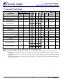
1
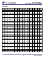
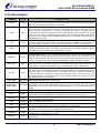
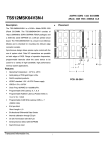
SP001GBLRU800S02
240pin DDR2 800 Unbuffered DIMM
SP001GBLRU800S02
240pin DDR2 SDRAM Unbuffered Module
SILICON POWER Computer and Communications, INC.
Corporate Office
7F, No. 106, Zhou-Z Street NeiHu Dist.,
Taipei 114,
Taiwan, R.O.C.
This document is a general product description and is subject to change without notice
Rev 1.0 Aug 2007
SP001GBLRU800S02
240pin DDR2 800 Unbuffered DIMM
Revision History
Revision No.
1.0
Date
2007/8/29
Remarks
First issue
Table of contents
1. Description...................................................................................................................................................... 2
2. Features ........................................................................................................................................................... 2
3. Module Specification.................................................................................................................................... 3
4. Simplified Mechanical Drawing with Keying Positions ...................................................................... 3
5. Pinouts ............................................................................................................................................................. 4
6. Pin Description .............................................................................................................................................. 5
7. Command Truth Table.................................................................................................................................. 6
8. Block Diagram................................................................................................................................................ 7
1
Rev 1.0 Aug 2007
SP001GBLRU800S02
240pin DDR2 800 Unbuffered DIMM
1. Description
The SP001GBLRU800S02 is a 128M x 8bits Double Data Rate SDRAM high-density for
DDR2-800. The SP001GBLRU800S02 consists of 8pcs CMOS 128Mx8 bits Double Data Rate
SDRAMs in 60 ball FBGA packages, and a 2048 bits serial EEPROM on a 240-pin printed
circuit board. The SP001GBLRU800S02 is a Dual In-Line Memory Module and is intended
for mounting into 240-pin edge connector sockets. Synchronous design allows precise
cycle control with the use of system clock. Data I/O transactions are possible on both
edges of DQS. Range of operation frequencies, programmable latencies allow the same
device to be useful for a variety of high bandwidth, high performance memory system
applications.
2. Features
․Fast data transfer rates: PC2-6400
․240-pin, unbuffered dual in-line memory module
․VDD = VDDQ = +1.8V, VDDSPD = +1.7V to +3.6V
․JEDEC standard 1.8V I/O (SSTL_18-compatible)
․Differential data strobe (DQS, DQS#) option
․Four-bit prefetch architecture
․DLL to align DQ and DQS transitions with CK
․Multiple internal device banks for concurrent operation
․Programmable CAS# latency (CL)
․Posted CAS# additive latency (AL)
․WRITE latency = READ latency - 1 tCK
․Programmable burst lengths: 4 or 8
․Adjustable data-output drive strength
․64ms, 8,192-cycle refresh
․On-die termination (ODT)
․60ball FBGA Leaded & Pb-Free (RoHS compliant) package
2
Rev 1.0 Aug 2007
SP001GBLRU800S02
240pin DDR2 800 Unbuffered DIMM
3. Module Specification
Item
Specification
Capacity
1024MByte
Physical Bank(s)
1
Module Organization
128M x 64bit
Module Type
Unbuffered Non ECC
Speed Grade
PC2-6400/CL=6,tRCD=6,tRP=6 (DDR2 800)
Voltage Interface
SSTL_18
Power Supply Voltage
1.8V±0.1V
Burst Lengths
DRAM Organization
4 or 8
128M x 8bit DDR2 SDRAM
PCB Layer
6Layers
Contact Tab
240 pin GOLD Flash Plating
Serial PD
Support
4. Simplified Mechanical Drawing with Keying Positions
Notes:1. All dimensions are in millimeters (inches); MAX/MIN or typical (TYP) where noted.
3
Rev 1.0 Aug 2007
SP001GBLRU800S02
240pin DDR2 800 Unbuffered DIMM
5. Pinouts
Pin
Num
Pin
Name
Pin
Num
Pin
Name
Pin
Num
Pin
Name
Pin
Num
Pin
Name
Pin
Num
Pin
Name
Pin
Num
Pin
Name
Pin
Num
Pin
Name
Pin
Num
Pin
Name
1
VREF
31
DQ19
61
A4
91
VSS
121
VSS
151
VSS
181
VDDQ
211
DM5
2
VSS
32
VSS
62
VDDQ
92
/DQS5
122
DQ4
152
DQ28
182
A3
212
NC
3
DQ0
33
DQ24
63
A2
93
DQS5
123
DQ5
153
DQ29
183
A1
213
VSS
4
DQ1
34
DQ25
64
VDD
94
VSS
124
VSS
154
VSS
184
VDD
214
DQ46
5
VSS
35
VSS
65
VSS
95
DQ42
125
DM0
155
DM3
185
CK0
215
DQ47
6
/DQS0
36
/DQS3
66
VSS
96
DQ43
126
NC
156
NC
186
/CK0
216
VSS
7
DQS0
37
DQS3
67
VDD
97
VSS
127
VSS
157
VSS
187
VDD
217
DQ52
8
VSS
38
VSS
68
NC
98
DQ48
128
DQ6
158
DQ30
188
A0
218
DQ53
9
DQ2
39
DQ26
69
VDD
99
DQ49
129
DQ7
159
DQ31
189
VDD
219
VSS
10
DQ3
40
DQ27
70
A10/AP 100
VSS
130
VSS
160
VSS
190
BA1
220
CK2
11
VSS
41
VSS
71
BA0
101
SA2
131
DQ12
161
NC
191
VDDQ
221
/CK2
12
DQ8
42
NC
72
VDDQ
102
NC
132
DQ13
162
NC
192
/RAS
222
VSS
13
DQ9
43
NC
73
/WE
103
VSS
133
VSS
163
VSS
193
/S0
223
DM6
14
VSS
44
VSS
74
/CAS
104
/DQS6
134
DM1
164
NC
194
VDDQ
224
NC
15
/DQS1
45
NC
75
VDDQ
105
DQS6
135
NC
165
NC
195
ODT0
225
VSS
16
DQS1
46
NC
76
/S1
106
VSS
136
VSS
166
VSS
196
A13
226
DQ54
17
VSS
47
VSS
77
ODT1
107
DQ50
137
CK1
167
NC
197
VDD
227
DQ55
18
NC
48
NC
78
VDDQ
108
DQ51
138
/CK1
168
NC
198
VSS
228
VSS
19
NC
49
NC
79
VSS
109
VSS
139
VSS
169
VSS
199
DQ36
229
DQ60
20
VSS
50
VSS
80
DQ32
110
DQ56
140
DQ14
170
VDDQ
200
DQ37
230
DQ61
21
DQ10
51
VDDQ
81
DQ33
111
DQ57
141
DQ15
171
CKE1
201
VSS
231
VSS
22
DQ11
52
CKE0
82
VSS
112
VSS
142
VSS
172
VDD
202
DM4
232
DM7
23
VSS
53
VDD
83
/DQS4
113
/DQS7
143
DQ20
173
A15
203
NC
233
NC
24
DQ16
54
NC
84
DQS4
114
DQS7
144
DQ21
174
A14
204
VSS
234
VSS
25
DQ17
55
NC
85
VSS
115
VSS
145
VSS
175
VDDQ
205
DQ38
235
DQ62
26
VSS
56
VDDQ
86
DQ34
116
DQ58
146
DM2
176
A12
206
DQ39
236
DQ63
27
/DQS2
57
A11
87
DQ35
117
DQ59
147
NC
177
A9
207
VSS
237
VSS
28
DQS2
58
A7
88
VSS
118
VSS
148
VSS
178
VDD
208
DQ44
238 VDDSPD
29
VSS
59
VDD
89
DQ40
119
SDA
149
DQ22
179
A8
209
DQ45
239
SA0
30
DQ18
60
A5
90
DQ41
120
SCL
150
DQ23
180
A6
210
VSS
240
SA1
4
Rev 1.0 Aug 2007
SP001GBLRU800S02
240pin DDR2 800 Unbuffered DIMM
6. Pin Description
SYMBOL
TYPE
CK, /CK
Input
CKE
Input
/S0
Input
ODT
Input
/RAS, /CAS, /WE
Input
DM0-DM7
Input
BA0 - BA2
Input
A0 - A15
Input
DQ0-DQ63
DQS0-DQS7
/DQS0-/DQS7
DESCRIPTION
Clock: CK and /CK are differential clock inputs. All address and control input signals are sampled
on the crossing of the positive edge of CK and negative edge of /CK. Output data (DQs and DQS
/DQS) is referenced to the crossings of CK and /CK.
Clock Enable: CKE HIGH activates, and CKE Low deactivates, internal clock signals and device
input buffers and output drivers. Taking CKE Low provides Precharge Power-Down and Self
Refresh operation (all banks idle), or Active Power-Down (row Active in any bank). CKE is
synchronous for power down entry and exit, and for self refresh entry. CKE is asynchronous for self
refresh exit. CKE must be maintained high throughout read and write accesses. Input buffers,
excluding CK, CK, ODT and CKE are disabled during power-down. Input buffers, excluding CKE, are
disabled during self refresh.
Chip Select: Enables the associated SDRAM command decoder when low and disables the
command decoder when high. When the command decoder is disabled, new commands are
ignored but previous operations continue. Rank 0 is selected by S0; Rank 1 is selected by S1
On Die Termination: ODT (registered HIGH) enables termination resistance internal to the DDR2
SDRAM. When enabled, ODT is only applied to the following pins: DQ, DQS, and /DQS. The ODT
input will be ignored if disabled via the LOAD MODE command.
Command Inputs: /RAS, /CAS and /WE (along with /CS) define the command being entered.
Input Data Mask: DM is an input mask signal for write data. Input data is masked when DM is
sampled HIGH coincident with that input data during a Write access. DM is sampled on both
edges of DQS. Although DM pins are input only, the DM loading matches the DQ and DQS
loading. For x8 device, the function of DM or RDQS/RDQS is enabled by EMRS command.
Bank Address Inputs: BA0 and BA1 for 256 and 512Mb, BA0 - BA2 define to which bank an
Active, Read, Write or Precharge command is being applied. Bank address also determines if the
mode register or extended mode register is to be accessed during a MRS or EMRS cycle.
Address Inputs: Provided the row address for Active commands and the column address and
Auto Precharge bit for Read/Write commands, to select one location out of the memory array in the
respective bank. A10 is sampled during a Precharge command to determine whether the
Precharge applies to one bank (A10 LOW) or all banks (A10 HIGH). If only one bank is to be
precharged, the bank is selected by BA0, BA1. The address inputs also provide the op-code
during Mode Register Set commands.
Input/Output Data bit Input/ Output: Bi-directional data bus.
Data Strobe: output with read data, input with write data for source-synchronous operation.
Edge-aligned with read data, center-aligned with write data. For Rawcards using x16 orginized
Input/Output
DRAMs DQ0-7 connect to the LDQS pin of the DRAMs and DQ8-17 connect to the UDQS pin of the
DRAM
NC
No Connect: No internal electrical connection is present.
VDDQ
Supply
VDD, VSS
Supply
VREF
Supply
SDA
Input/Output
SCL
Input
VDDSPD
Supply
SA0-SA2
Input
Power supplies for the DDR2 SDRAM output buffers to provide improved noise immunity. For all
current DDR2 unbuffered DIMM designs, VDDQ shares the same power plane as VDD pins
Power and ground for the DDR2 SDRAM input buffers, and core logic. VDD and VDDQ pins are tied to
VDD / VDDQ planes on these modules.
Reference voltage for SSTL 18 inputs.
This bidirectional pin is used to transfer data into or out of the SPD EEPROM. A resistor must be
connected from the SDA bus line to VDD to act as a pullup on the system board.
This signal is used to clock data into and out of the SPD EEPROM. A resistor may be connected
from the SCL bus time to VDD to act as a pullup onthe system board.
Power supply for SPD EEPROM. This supply is separate from the VDD / VDDQ power plane.
EEPROM supply is operable from 1.7V to 3.6V.
These signals and tied at the system planar to either VSS or VDD to configure the serial SPD EERPOM
address range
5
Rev 1.0 Aug 2007
SP001GBLRU800S02
240pin DDR2 800 Unbuffered DIMM
7. Command Truth Table
Command
CKE
Previous Current
Cycle
Cycle
CS RAS CAS WE
BA0
,BA1
A10
A15-A11
,A9-A0
Note
(Extended) Mode Register Set
H
H
L
L
L
L
BA
Auto-Refresh
H
H
L
L
L
H
X
X
X
1
Self Refresh Entry
H
L
L
L
L
H
X
X
X
1
H
X
X
X
Self Refresh Exit
L
H
X
X
X
1
L
H
H
H
OP Code
1,2
Single Bank Precharge
H
H
L
L
H
L
BA
L
X
1,2
Precharge all Banks
H
H
L
L
H
L
X
H
X
1
Bank Activate
H
H
L
L
H
H
BA
Write
H
H
L
H
L
L
BA
L
Column Address
1,2,3
Write with Auto Precharge
H
H
L
H
L
L
BA
H
Column Address
1,2,3
Read
H
H
L
H
L
H
BA
L
Column Address
1,2,3
Read with Auto-Precharge
H
H
L
H
L
H
BA
H
Column Address
1,2,3
No Operation
H
X
L
H
H
H
X
X
X
1
Device Deselect
H
X
H
X
X
X
X
X
X
1
H
X
X
X
Power Down Entry
H
L
X
X
X
1,4
L
H
H
H
H
X
X
X
X
X
X
1,4
L
H
H
H
Power Down Exit
L
H
Row Address
1,2
(H=Logic High Level, L=Logic Low Level, X=Don’t Care, OP Code=Operand Code)
NOTE:1. All DDR2 SDRAM commands are defined by states of /CS, /WE, /RAS, /CAS, and CKE at the rising edge of the clock.
2. Bank addresses (BA0, BA1) determine which bank is to be operated upon. For (E)MRS BA selects an (Extended) Mode
Register.
3. Burst reads or writes at BL = 4 cannot be terminated. See sections “Reads interrupted by a Read” and “Writes interrupted
by a Write”.
4. The Power Down Mode does not perform any refresh operations. The duration of Power Down is therefore limited by the
refresh requirements.
6
Rev 1.0 Aug 2007
SP001GBLRU800S02
240pin DDR2 800 Unbuffered DIMM
8. Block Diagram
7
Rev 1.0 Aug 2007