1
Intel® Xeon® Processor E5-1600/
E5-2600/E5-4600 Product Families
Datasheet - Volume One
May 2012
Reference Number: 326508, Revision: 002
INFORMATION IN THIS DOCUMENT IS PROVIDED IN CONNECTION WITH INTEL PRODUCTS. NO LICENSE, EXPRESS OR IMPLIED,
BY ESTOPPEL OR OTHERWISE, TO ANY INTELLECTUAL PROPERTY RIGHTS IS GRANTED BY THIS DOCUMENT. EXCEPT AS
PROVIDED IN INTEL'S TERMS AND CONDITIONS OF SALE FOR SUCH PRODUCTS, INTEL ASSUMES NO LIABILITY WHATSOEVER
AND INTEL DISCLAIMS ANY EXPRESS OR IMPLIED WARRANTY, RELATING TO SALE AND/OR USE OF INTEL PRODUCTS INCLUDING
LIABILITY OR WARRANTIES RELATING TO FITNESS FOR A PARTICULAR PURPOSE, MERCHANTABILITY, OR INFRINGEMENT OF ANY
PATENT, COPYRIGHT OR OTHER INTELLECTUAL PROPERTY RIGHT.
INFORMATION
SALE
UNLESS
AND/OR
OTHERWISE
USE
IN THIS
OFAGREED
INTEL
DOCUMENT
PRODUCTS
IN WRITING
IS PROVIDED
INCLUDING
BY INTEL,
IN CONNECTION
LIABILITY
THE INTELOR
PRODUCTS
WITH
WARRANTIES
Intel®
AREPRODUCTS.
NOT
RELATING
DESIGNED
TO
NOFITNESS
LICENSE,
NOR INTENDED
FOR
Express*
A PARTICULAR
FOR
ORANY
IMPLIED,
APPLICATION
PURPOSE,
BY ESTOPPEL
MERCHANTABILITY,
IN WHICH
OR OTHERWISE,
THE FAILURE
OR INFRINGEMENT
TOOF
ANY
THE
INTELLECTUAL
INTELOF
PRODUCT
ANY PATENT,
PROPERTY
COULD
COPYRIGHT
RIGHTS
CREATE IS
A OR
SITUATION
GRANTED
OTHER INTELLECTUAL
BY
WHERE
THIS PERSONAL
DOCUMENT.
PROPERTY
INJURY
EXCEPT
RIGHT.
OR
ASDEATH
PROVIDED
MAY OCCUR.
IN INTEL'S TERMS AND CONDITIONS OF SALE FOR SUCH PRODUCTS, INTEL ASSUMES NO LIABILITY WHATSOEVER, AND INTEL DISCLAIMS ANY Express* OR IMPLIED WARRANTY, RELATING TO
UNLESS OTHERWISE AGREED IN WRITING BY INTEL, THE INTEL PRODUCTS ARE NOT DESIGNED NOR INTENDED FOR ANY
APPLICATION IN WHICH THE FAILURE OF THE INTEL PRODUCT COULD CREATE A SITUATION WHERE PERSONAL INJURY OR DEATH
MAY OCCUR.
Intel may make changes to specifications and product descriptions at any time, without notice. Designers must not rely on the
absence or characteristics of any features or instructions marked "reserved" or "undefined." Intel reserves these for future
definition and shall have no responsibility whatsoever for conflicts or incompatibilities arising from future changes to them. The
information here is subject to change without notice. Do not finalize a design with this information.
The Intel® Xeon® Processor E5-1600/ E5-2600/E5-4600 Product Families, Intel® C600 series chipset, and the Intel® Xeon®
Processor E5-1600/ E5-2600/E5-4600 Product Families-based Platform described in this document may contain design defects or
errors known as errata which may cause the product to deviate from published specifications. Current characterized errata are
available on request.
Contact your local Intel sales office or your distributor to obtain the latest specifications and before placing your product order.
Copies of documents which have an order number and are referenced in this document, or other Intel literature, may be obtained
by calling 1-800-548-4725, or go to: http://www.intel.com/#/en_US_01
Hyper-Threading Technology requires a computer system with a processor supporting HT Technology and an HT Technology
enabled chipset, BIOS and operating system. Performance will vary depending on the specific hardware and software you use. For
more information including details on which processors support HT Technology, see
http://www.intel.com/products/ht/hyperthreading_more.htm.
Enabling Execute Disable Bit functionality requires a PC with a processor with Execute Disable Bit capability and a supporting
operating system. Check with your PC manufacturer on whether your system delivers Execute Disable Bit functionality.
Intel® Virtualization Technology requires a computer system with an enabled Intel® processor, BIOS, virtual machine monitor
(VMM) and, for some uses, certain computer system software enabled for it. Functionality, performance or other benefits will vary
depending on hardware and software configurations and may require a BIOS update. Software applications may not be compatible
with all operating systems. Please check with your application vendor.
Intel® Turbo Boost Technology requires a PC with a processor with Intel Turbo Boost Technology capability. Intel Turbo Boost
Technology performance varies depending on hardware, software and overall system configuration. Check with your PC
manufacturer on whether your system delivers Intel Turbo Boost Technology. For more information, see
http://www.intel.com/technology/turboboost/.
64-bit computing on Intel architecture requires a computer system with a processor, chipset, BIOS, operating system, device
drivers and applications enabled for Intel® 64 architecture. Performance will vary depending on your hardware and software
configurations. Consult with your system vendor for more information.
Δ Intel processor numbers are not a measure of performance. Processor numbers differentiate features within each processor
family, not across different processor families. See http://www.intel.com/products/processor%5Fnumber/ for details.
I2C is a two-wire communications bus/protocol developed by Philips. SMBus is a subset of the I2C bus/protocol and was developed
by Intel. Implementations of the I2C bus/protocol may require licenses from various entities, including Philips Electronics N.V. and
North American Philips Corporation.
Intel, Xeon, Intel SpeedStep, Intel Core, and the Intel logo are trademarks of Intel Corporation in the U. S. and other countries.
*Other names and brands may be claimed as the property of others.
Copyright © 2009-2012, Intel Corporation. All rights reserved.
2
Intel® Xeon® Processor E5-1600/ E5-2600/E5-4600 Product Families
Datasheet Volume One
Contents
1
Overview ................................................................................................................. 13
1.1
Introduction ..................................................................................................... 13
1.1.1 Processor Feature Details ........................................................................ 14
1.1.2 Supported Technologies .......................................................................... 14
1.2
Interfaces ........................................................................................................ 15
1.2.1 System Memory Support ......................................................................... 15
1.2.2 PCI Express* ......................................................................................... 16
1.2.3 Direct Media Interface Gen 2 (DMI2)......................................................... 17
1.2.4 Intel® QuickPath Interconnect (Intel® QPI) .............................................. 18
1.2.5 Platform Environment Control Interface (PECI) ........................................... 18
1.3
Power Management Support ............................................................................... 19
1.3.1 Processor Package and Core States........................................................... 19
1.3.2 System States Support ........................................................................... 19
1.3.3 Memory Controller.................................................................................. 19
1.3.4 PCI Express ........................................................................................... 19
1.3.5 Intel QPI ............................................................................................... 19
1.4
Thermal Management Support ............................................................................ 19
1.5
Package Summary............................................................................................. 20
1.6
Terminology ..................................................................................................... 20
1.7
Related Documents ........................................................................................... 22
1.8
State of Data .................................................................................................... 23
2
Interfaces................................................................................................................ 25
2.1
System Memory Interface .................................................................................. 25
2.1.1 System Memory Technology Support ........................................................ 25
2.1.2 System Memory Timing Support............................................................... 25
2.2
PCI Express* Interface....................................................................................... 26
2.2.1 PCI Express* Architecture ....................................................................... 26
2.2.2 PCI Express* Configuration Mechanism ..................................................... 27
2.3
DMI2/PCI Express* Interface .............................................................................. 28
2.3.1 DMI2 Error Flow ..................................................................................... 28
2.3.2 Processor/PCH Compatibility Assumptions.................................................. 28
2.3.3 DMI2 Link Down..................................................................................... 28
2.4
Intel QuickPath Interconnect............................................................................... 28
2.5
Platform Environment Control Interface (PECI) ...................................................... 30
2.5.1 PECI Client Capabilities ........................................................................... 30
2.5.2 Client Command Suite ............................................................................ 31
2.5.3 Client Management................................................................................. 69
2.5.4 Multi-Domain Commands ........................................................................ 74
2.5.5 Client Responses .................................................................................... 75
2.5.6 Originator Responses .............................................................................. 76
2.5.7 DTS Temperature Data ........................................................................... 76
3
Technologies ........................................................................................................... 79
3.1
Intel® Virtualization Technology (Intel® VT) ........................................................ 79
3.1.1 Intel VT-x Objectives .............................................................................. 79
3.1.2 Intel VT-x Features................................................................................. 80
3.1.3 Intel VT-d Objectives .............................................................................. 80
3.1.4 Intel Virtualization Technology Processor Extensions ................................... 81
3.2
Security Technologies ........................................................................................ 81
3.2.1 Intel® Trusted Execution Technology........................................................ 81
3.2.2 Intel Trusted Execution Technology – Server Extensions .............................. 82
3.2.3 Intel® Advanced Encryption Standard Instructions (Intel® AES-NI).............. 82
Intel® Xeon® Processor E5-1600/ E5-2600/E5-4600 Product Families
Datasheet Volume One
3
3.3
3.4
3.5
3.6
3.7
3.8
3.2.4 Execute Disable Bit .................................................................................83
Intel® Hyper-Threading Technology .....................................................................83
Intel® Turbo Boost Technology ...........................................................................83
3.4.1 Intel® Turbo Boost Operating Frequency ...................................................83
Enhanced Intel SpeedStep® Technology ...............................................................84
Intel® Intelligent Power Technology.....................................................................84
Intel® Advanced Vector Extensions (Intel® AVX) ..................................................84
Intel Dynamic Power Technology .........................................................................85
4
Power Management .................................................................................................87
4.1
ACPI States Supported .......................................................................................87
4.1.1 System States........................................................................................87
4.1.2 Processor Package and Core States ...........................................................87
4.1.3 Integrated Memory Controller States .........................................................88
4.1.4 DMI2/PCI Express* Link States.................................................................89
4.1.5 Intel QuickPath Interconnect States ..........................................................89
4.1.6 G, S, and C State Combinations................................................................90
4.2
Processor Core/Package Power Management .........................................................90
4.2.1 Enhanced Intel SpeedStep Technology.......................................................90
4.2.2 Low-Power Idle States.............................................................................91
4.2.3 Requesting Low-Power Idle States ............................................................92
4.2.4 Core C-states .........................................................................................92
4.2.5 Package C-States ...................................................................................94
4.2.6 Package C-State Power Specifications........................................................97
4.3
System Memory Power Management ....................................................................98
4.3.1 CKE Power-Down ....................................................................................98
4.3.2 Self Refresh ...........................................................................................98
4.3.3 DRAM I/O Power Management ..................................................................99
4.4
DMI2/PCI Express* Power Management ................................................................99
5
Thermal Management Specifications ...................................................................... 101
5.1
Package Thermal Specifications ......................................................................... 101
5.1.1 Thermal Specifications........................................................................... 101
5.1.2 TCASE and DTS Based Thermal Specifications........................................... 103
5.1.3 Processor Thermal Profiles ..................................................................... 104
5.1.4 Embedded Server Processor Thermal Profiles............................................ 130
5.1.5 Thermal Metrology ................................................................................ 133
5.2
Processor Core Thermal Features ....................................................................... 135
5.2.1 Processor Temperature.......................................................................... 135
5.2.2 Adaptive Thermal Monitor ...................................................................... 135
5.2.3 On-Demand Mode ................................................................................. 137
5.2.4 PROCHOT_N Signal ............................................................................... 137
5.2.5 THERMTRIP_N Signal ............................................................................ 138
5.2.6 Integrated Memory Controller (IMC) Thermal Features............................... 138
6
Signal Descriptions ................................................................................................ 141
6.1
System Memory Interface Signals ...................................................................... 141
6.2
PCI Express* Based Interface Signals ................................................................. 142
6.3
DMI2/PCI Express* Port 0 Signals ...................................................................... 144
6.4
Intel QuickPath Interconnect Signals .................................................................. 144
6.5
PECI Signal ..................................................................................................... 145
6.6
System Reference Clock Signals ........................................................................ 145
6.7
JTAG and TAP Signals....................................................................................... 145
6.8
Serial VID Interface (SVID) Signals .................................................................... 146
6.9
Processor Asynchronous Sideband and Miscellaneous Signals................................. 146
6.10 Processor Power and Ground Supplies ................................................................ 149
4
Intel® Xeon® Processor E5-1600/ E5-2600/E5-4600 Product Families
Datasheet Volume One
7
Electrical Specifications ......................................................................................... 151
7.1
Processor Signaling ......................................................................................... 151
7.1.1 System Memory Interface Signal Groups ................................................. 151
7.1.2 PCI Express* Signals ............................................................................ 151
7.1.3 DMI2/PCI Express* Signals.................................................................... 151
7.1.4 Intel QuickPath Interconnect (Intel QPI) .................................................. 151
7.1.5 Platform Environmental Control Interface (PECI) ...................................... 152
7.1.6 System Reference Clocks (BCLK{0/1}_DP, BCLK{0/1}_DN)....................... 152
7.1.7 JTAG and Test Access Port (TAP) Signals ................................................. 153
7.1.8 Processor Sideband Signals ................................................................... 153
7.1.9 Power, Ground and Sense Signals........................................................... 153
7.1.10 Reserved or Unused Signals................................................................... 158
7.2
Signal Group Summary .................................................................................... 158
7.3
Power-On Configuration (POC) Options............................................................... 162
7.4
Fault Resilient Booting (FRB)............................................................................. 163
7.5
Mixing Processors............................................................................................ 163
7.6
Flexible Motherboard Guidelines (FMB) ............................................................... 164
7.7
Absolute Maximum and Minimum Ratings ........................................................... 164
7.7.1 Storage Conditions Specifications ........................................................... 165
7.8
DC Specifications ............................................................................................ 166
7.8.1 Voltage and Current Specifications.......................................................... 167
7.8.2 Die Voltage Validation ........................................................................... 173
7.8.3 Signal DC Specifications ........................................................................ 174
7.9
Waveforms..................................................................................................... 180
7.10 Signal Quality ................................................................................................. 181
7.10.1 DDR3 Signal Quality Specifications ......................................................... 182
7.10.2 I/O Signal Quality Specifications............................................................. 182
7.10.3 Intel QuickPath Interconnect Signal Quality Specifications.......................... 182
7.10.4 Input Reference Clock Signal Quality Specifications................................... 182
7.10.5 Overshoot/Undershoot Tolerance............................................................ 182
8
Processor Land Listing........................................................................................... 187
8.1
Listing by Land Name ...................................................................................... 187
8.2
Listing by Land Number ................................................................................... 212
9
Package Mechanical Specifications ........................................................................ 237
9.1
Package Mechanical Drawing............................................................................. 237
9.2
Processor Component Keep-Out Zones ............................................................... 241
9.3
Package Loading Specifications ......................................................................... 241
9.4
Package Handling Guidelines............................................................................. 241
9.5
Package Insertion Specifications........................................................................ 241
9.6
Processor Mass Specification ............................................................................. 242
9.7
Processor Materials.......................................................................................... 242
9.8
Processor Markings.......................................................................................... 242
10
Boxed Processor Specifications ............................................................................. 243
10.1 Introduction ................................................................................................... 243
10.1.1 Available Boxed Thermal Solution Configurations ...................................... 243
10.1.2 Intel Thermal Solution STS200C
(Passive/Active Combination Heat Sink Solution) ...................................... 243
10.1.3 Intel Thermal Solution STS200P and STS200PNRW
(Boxed 25.5 mm Tall Passive Heat Sink Solutions).................................... 244
10.2 Mechanical Specifications ................................................................................. 245
10.2.1 Boxed Processor Heat Sink Dimensions and Baseboard Keepout Zones ........ 245
10.2.2 Boxed Processor Retention Mechanism and Heat Sink Support (ILM-RS) ...... 254
10.3 Fan Power Supply [STS200C]............................................................................ 254
10.3.1 Boxed Processor Cooling Requirements ................................................... 255
10.4 Boxed Processor Contents ................................................................................ 257
Intel® Xeon® Processor E5-1600/ E5-2600/E5-4600 Product Families
Datasheet Volume One
5
Figures
1-1
1-2
2-1
2-2
2-3
2-4
2-5
2-6
2-7
2-8
2-9
2-10
2-11
2-12
2-13
2-14
2-15
2-16
2-17
2-18
2-19
2-20
2-21
2-22
2-23
2-24
2-25
2-26
2-27
2-28
2-29
2-30
2-31
2-32
2-33
2-34
2-35
2-36
2-37
2-38
2-39
2-40
2-41
2-42
2-43
2-44
2-45
2-46
6
Intel® Xeon® Processor E5-2600 Product Family on the 2 Socket
Platform ...........................................................................................................14
PCI Express* Lane Partitioning and Direct Media Interface Gen 2 (DMI2)...................17
PCI Express* Layering Diagram ...........................................................................26
Packet Flow through the Layers ...........................................................................27
Ping() ..............................................................................................................32
Ping() Example..................................................................................................32
GetDIB() ..........................................................................................................32
Device Info Field Definition .................................................................................33
Revision Number Definition .................................................................................33
GetTemp()........................................................................................................34
GetTemp() Example ...........................................................................................35
RdPkgConfig() ...................................................................................................36
WrPkgConfig()...................................................................................................37
DRAM Thermal Estimation Configuration Data........................................................40
DRAM Rank Temperature Write Data ....................................................................41
The Processor DIMM Temperature Read / Write .....................................................42
Ambient Temperature Reference Data ..................................................................42
Processor DRAM Channel Temperature .................................................................43
Accumulated DRAM Energy Data..........................................................................43
DRAM Power Info Read Data ...............................................................................44
DRAM Power Limit Data ......................................................................................45
DRAM Power Limit Performance Data....................................................................45
CPUID Data ......................................................................................................49
Platform ID Data ...............................................................................................49
PCU Device ID...................................................................................................49
Maximum Thread ID...........................................................................................50
Processor Microcode Revision ..............................................................................50
Machine Check Status ........................................................................................50
Package Power SKU Unit Data .............................................................................50
Package Power SKU Data ....................................................................................52
Package Temperature Read Data .........................................................................52
Temperature Target Read ...................................................................................53
Thermal Status Word .........................................................................................54
Thermal Averaging Constant Write / Read .............................................................54
Current Config Limit Read Data ...........................................................................55
Accumulated Energy Read Data ...........................................................................55
Power Limit Data for VCC Power Plane ..................................................................56
Package Turbo Power Limit Data ..........................................................................57
Package Power Limit Performance Data ................................................................57
Efficient Performance Indicator Read ....................................................................58
ACPI P-T Notify Data ..........................................................................................58
Caching Agent TOR Read Data.............................................................................59
DTS Thermal Margin Read...................................................................................59
Processor ID Construction Example ......................................................................61
RdIAMSR()........................................................................................................61
PCI Configuration Address...................................................................................64
RdPCIConfig() ...................................................................................................64
PCI Configuration Address for local accesses..........................................................66
Intel® Xeon® Processor E5-1600/ E5-2600/E5-4600 Product Families
Datasheet Volume One
2-47
2-48
2-49
2-50
4-1
4-2
4-3
5-1
5-2
5-3
5-4
5-5
5-6
5-7
5-8
5-9
5-10
5-11
5-12
5-13
5-14
5-15
5-16
5-17
5-18
5-19
5-20
5-21
5-22
5-23
5-24
5-25
5-26
5-27
5-28
5-29
7-1
7-2
7-3
7-4
7-5
7-6
7-7
7-8
7-9
RdPCIConfigLocal()............................................................................................ 66
WrPCIConfigLocal() ........................................................................................... 68
The Processor PECI Power-up Timeline() .............................................................. 70
Temperature Sensor Data Format........................................................................ 76
Idle Power Management Breakdown of the Processor Cores..................................... 91
Thread and Core C-State Entry and Exit ............................................................... 91
Package C-State Entry and Exit ........................................................................... 95
Tcase: 8-Core 150W Thermal Profile, Workstation Platform SKU Only ..................... 105
DTS: 8-Core 150W Thermal Profile, Workstation Platform SKU Only ....................... 105
Tcase: 8-Core 135W Thermal Profile 2U ............................................................. 107
DTS: 8-Core 135W Thermal Profile 2U................................................................ 108
Tcase: 8/6-Core 130W Thermal Profile 1U .......................................................... 110
DTS: 8-Core 130W Thermal Profile 1U................................................................ 110
DTS: 6-Core 130W Thermal Profile 1U................................................................ 111
Tcase: 6-Core 130W 1S WS Thermal Profile ........................................................ 112
DTS: 6-Core 130W 1S WS Thermal Profile .......................................................... 113
Tcase: 8-Core 115W Thermal Profile 1U ............................................................. 115
DTS: 8-Core 115W Thermal Profile 1U................................................................ 115
Tcase: 8/6-Core 95W Thermal Profile 1U ............................................................ 117
DTS: 8-Core 95W Thermal Profile 1U ................................................................. 117
DTS: 6-Core 95W Thermal Profile 1U ................................................................. 118
Tcase: 8-Core 70W Thermal Profile 1U ............................................................... 119
DTS: 8-Core 70W Thermal Profile 1U ................................................................. 120
Tcase: 6-Core 60W Thermal Profile 1U ............................................................... 121
DTS: 6-Core 60W Thermal Profile 1U ................................................................. 122
Tcase: 4-Core 130W Thermal Profile 2U ............................................................. 123
DTS: 4-Core 130W Thermal Profile 2U................................................................ 124
Tcase: 4-Core 130W 1S WS Thermal Profile ........................................................ 126
DTS: 4-Core 130W 1S WS Thermal Profile .......................................................... 126
Tcase: 4/2-Core 80W Thermal Profile 1U ............................................................ 128
DTS: 4-Core 80W Thermal Profile 1U ................................................................. 128
DTS: 2-Core 80W Thermal Profile 1U ................................................................. 129
Tcase: 8-Core LV95W Thermal Profile, Embedded Server SKU ............................... 131
Tcase: 8-Core LV70W Thermal Profile, Embedded Server SKU ............................... 132
Case Temperature (TCASE) Measurement Location .............................................. 134
Frequency and Voltage Ordering........................................................................ 136
Input Device Hysteresis ................................................................................... 152
VR Power-State Transitions............................................................................... 156
8/6-Core: VCC Static and Transient Tolerance Loadlines ....................................... 170
4/2-Core: Processor VCC Static and Transient Tolerance Loadlines ......................... 172
Load Current Versus Time ................................................................................ 173
VCC Overshoot Example Waveform.................................................................... 174
BCLK{0/1} Differential Clock Crosspoint Specification .......................................... 180
BCLK{0/1} Differential Clock Measurement Point for Ringback .............................. 180
BCLK{0/1} Single Ended Clock Measurement Points for Absolute Cross Point
and Swing ...................................................................................................... 181
7-10 BCLK{0/1} Single Ended Clock Measurement Points for Delta Cross Point ............... 181
7-11 Maximum Acceptable Overshoot/Undershoot Waveform........................................ 185
9-1
Processor Package Assembly Sketch .................................................................. 237
9-2
Processor Package Drawing Sheet 1 of 2 ............................................................ 239
9-3
Processor Package Drawing Sheet 2 of 2 ............................................................ 240
9-4
Processor Top-Side Markings ........................................................................... 242
Intel® Xeon® Processor E5-1600/ E5-2600/E5-4600 Product Families
Datasheet Volume One
7
10-1
10-2
10-3
10-4
10-5
10-6
10-7
10-8
10-9
10-10
10-11
10-12
STS200C Passive/Active Combination Heat Sink (with Removable Fan) ................... 244
STS200C Passive/Active Combination Heat Sink (with Fan Removed)...................... 244
STS200P and STS200PNRW 25.5 mm Tall Passive Heat Sinks ................................ 245
Boxed Processor Motherboard Keepout Zones (1 of 4) .......................................... 246
Boxed Processor Motherboard Keepout Zones (2 of 4) .......................................... 247
Boxed Processor Motherboard Keepout Zones (3 of 4) .......................................... 248
Boxed Processor Motherboard Keepout Zones (4 of 4) .......................................... 249
Boxed Processor Heat Sink Volumetric (1 of 2) .................................................... 250
Boxed Processor Heat Sink Volumetric (2 of 2) .................................................... 251
4-Pin Fan Cable Connector (For Active Heat Sink) ................................................ 252
4-Pin Base Baseboard Fan Header (For Active Heat Sink) ..................................... 253
Fan Cable Connector Pin Out For 4-Pin Active Thermal Solution............................. 255
Tables
1-1
2-1
2-2
2-3
2-4
2-5
2-6
2-7
2-8
2-9
2-10
2-11
2-12
2-13
2-14
2-15
2-16
2-17
2-18
2-19
2-20
2-21
2-22
2-23
2-24
4-1
4-2
4-3
4-4
4-5
4-6
4-7
4-8
4-9
8
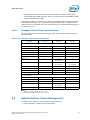
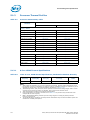
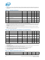
Referenced Documents .......................................................................................22
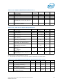
Summary of Processor-specific PECI Commands ....................................................30
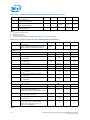
Minor Revision Number Meaning ..........................................................................33
GetTemp() Response Definition ...........................................................................35
RdPkgConfig() Response Definition.......................................................................36
WrPkgConfig() Response Definition ......................................................................37
RdPkgConfig() & WrPkgConfig() DRAM Thermal and Power Optimization
Services Summary .............................................................................................39
Channel & DIMM Index Decoding .........................................................................41
RdPkgConfig() & WrPkgConfig() CPU Thermal and Power Optimization
Services Summary .............................................................................................46
Power Control Register Unit Calculations ...............................................................51
RdIAMSR() Response Definition ...........................................................................62
RdIAMSR() Services Summary.............................................................................62
RdPCIConfig() Response Definition .......................................................................65
RdPCIConfigLocal() Response Definition ................................................................67
WrPCIConfigLocal() Response Definition................................................................68
WrPCIConfigLocal() Memory Controller and IIO Device/Function Support...................69
PECI Client Response During Power-Up .................................................................69
SOCKET ID Strapping .........................................................................................71
Power Impact of PECI Commands vs. C-states.......................................................71
Domain ID Definition..........................................................................................74
Multi-Domain Command Code Reference...............................................................74
Completion Code Pass/Fail Mask ..........................................................................75
Device Specific Completion Code (CC) Definition ....................................................75
Originator Response Guidelines............................................................................76
Error Codes and Descriptions...............................................................................77
System States...................................................................................................87
Package C-State Support ....................................................................................87
Core C-State Support .........................................................................................88
System Memory Power States .............................................................................88
DMI2/PCI Express* Link States............................................................................89
Intel QPI States.................................................................................................89
G, S and C State Combinations............................................................................90
P_LVLx to MWAIT Conversion ..............................................................................92
Coordination of Core Power States at the Package Level..........................................95
Intel® Xeon® Processor E5-1600/ E5-2600/E5-4600 Product Families
Datasheet Volume One
4-10
5-1
5-2
5-3
5-4
5-5
5-6
5-7
5-8
5-9
5-10
5-11
5-12
5-13
5-14
5-15
5-16
5-17
5-18
5-19
5-20
5-21
5-22
5-23
5-24
5-25
5-26
5-27
5-28
6-1
6-2
6-3
6-4
6-5
6-6
6-7
6-8
6-9
6-10
6-11
6-12
6-13
6-14
6-15
6-16
7-1
7-2
7-3
7-4
7-5
7-6
7-7
Package C-State Power Specifications .................................................................. 97
Processor SKU Summary Table ......................................................................... 104
Tcase: 8-Core 150W Thermal Specifications, Workstation Platform SKU Only........... 104
8-Core 150W Thermal Profile, Workstation Platform SKU Only ............................. 106
Tcase: 8-Core 135W Thermal Specifications 2U ................................................... 107
8-Core 135W Thermal Profile Table 2U ............................................................... 108
Tcase: 8/6-Core 130W Thermal Specifications, Workstation/Server Platform ........... 109
8/6-Core 130W Thermal Profile Table 1U ............................................................ 111
Tcase: 6-Core 130W 1S WS Thermal Specifications.............................................. 112
6-Core 130W 1S WS Thermal Profile Table.......................................................... 113
Tcase: 8-Core 115W Thermal Specifications 1U ................................................... 114
8-Core 115W Thermal Profile Table 1U ............................................................... 116
Tcase: 8/6-Core 95W Thermal Specifications, Workstation/Server Platform ............. 116
8/6-Core 95W Thermal Profile Table 1U.............................................................. 118
Tcase: 8-Core 70W Thermal Specifications 1U ..................................................... 119
8-Core 70W Thermal Profile Table 1U................................................................. 120
Tcase: 6-Core 60W Thermal Specifications 1U ..................................................... 121
6-Core 60W Thermal Profile Table 1U................................................................. 122
Tcase: 4-Core 130W Thermal Specifications 2U ................................................... 123
4-Core 130W Thermal Profile Table 2U ............................................................... 124
Tcase: 4-Core 130W 1S WS Thermal Specifications, Workstation/Server Platform .... 125
4-Core 130W 1S WS Thermal Profile Table.......................................................... 127
Tcase: 4/2-Core 80W Thermal Specifications 1U .................................................. 127
4/2-Core 80W Thermal Profile Table 1U.............................................................. 129
Embedded Server Processor Elevated Tcase SKU Summary Table .......................... 130
Tcase: 8-Core LV95W Thermal Specifications, Embedded Server SKU ..................... 130
8-Core LV95W Thermal Profile Table, Embedded Server SKU................................. 131
Tcase: 8-Core LV70W Thermal Specifications, Embedded Server SKU ..................... 132
8-Core LV70W Thermal Profile Table, Embedded Server SKU................................. 133
Memory Channel DDR0, DDR1, DDR2, DDR3....................................................... 141
Memory Channel Miscellaneous ......................................................................... 142
PCI Express* Port 1 Signals .............................................................................. 142
PCI Express* Port 2 Signals .............................................................................. 142
PCI Express* Port 3 Signals .............................................................................. 143
PCI Express* Miscellaneous Signals ................................................................... 143
DMI2 and PCI Express* Port 0 Signals................................................................ 144
Intel QPI Port 0 and 1 Signals ........................................................................... 144
Intel QPI Miscellaneous Signals ......................................................................... 144
PECI Signals ................................................................................................... 145
System Reference Clock (BCLK{0/1}) Signals ..................................................... 145
JTAG and TAP Signals ...................................................................................... 145
SVID Signals .................................................................................................. 146
Processor Asynchronous Sideband Signals .......................................................... 146
Miscellaneous Signals ...................................................................................... 148
Power and Ground Signals ................................................................................ 149
Power and Ground Lands.................................................................................. 154
SVID Address Usage ........................................................................................ 157
VR12.0 Reference Code Voltage Identification (VID) Table .................................... 157
Signal Description Buffer Types ......................................................................... 158
Signal Groups ................................................................................................. 159
Signals with On-Die Termination ....................................................................... 162
Power-On Configuration Option Lands ................................................................ 162
Intel® Xeon® Processor E5-1600/ E5-2600/E5-4600 Product Families
Datasheet Volume One
9
7-8
7-9
7-10
7-11
7-12
7-13
7-14
7-15
7-16
7-17
7-18
7-19
7-20
7-21
7-22
7-23
7-24
7-25
8-1
8-2
9-1
9-2
9-3
10-1
10-2
10-3
10
Fault Resilient Booting (Output Tri-State) Signals ................................................. 163
Processor Absolute Minimum and Maximum Ratings ............................................. 164
Storage Condition Ratings................................................................................. 165
Voltage Specification ........................................................................................ 167
Processor Current Specifications ........................................................................ 168
8/6 Core: Processor VCC Static and Transient Tolerance ....................................... 169
4/2-Core: Processor VCC Static and Transient Tolerance ....................................... 170
VCC Overshoot Specifications ............................................................................ 173
DDR3 and DDR3L Signal DC Specifications .......................................................... 174
PECI DC Specifications ..................................................................................... 176
System Reference Clock (BCLK{0/1}) DC Specifications........................................ 176
SMBus DC Specifications................................................................................... 176
JTAG and TAP Signals DC Specifications .............................................................. 177
Serial VID Interface (SVID) DC Specifications ...................................................... 177
Processor Asynchronous Sideband DC Specifications............................................. 178
Miscellaneous Signals DC Specifications .............................................................. 179
Processor I/O Overshoot/Undershoot Specifications .............................................. 182
Processor Sideband Signal Group Overshoot/Undershoot Tolerance ........................ 184
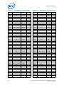
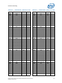
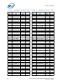
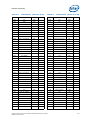
Land Name ..................................................................................................... 187
Land Number .................................................................................................. 212
Processor Loading Specifications ........................................................................ 241
Package Handling Guidelines ............................................................................. 241
Processor Materials .......................................................................................... 242
PWM Fan Frequency Specifications For 4-Pin Active Thermal Solution...................... 254
8 Core / 6 Core Server Thermal Solution Boundary Conditions ............................... 256
4 Core Server Thermal Solution Boundary Conditions ........................................... 256
Intel® Xeon® Processor E5-1600/ E5-2600/E5-4600 Product Families
Datasheet Volume One
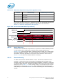
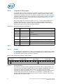
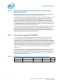
Revision History
Revision
Number
Description
Revision Date
001
Initial Release
March 2012
002
Added Intel® Xeon® Processor E5-4600 Product Family
May 2012
§
Intel® Xeon® Processor E5-1600/ E5-2600/E5-4600 Product Families
Datasheet Volume One
11
12
Intel® Xeon® Processor E5-1600/ E5-2600/E5-4600 Product Families
Datasheet Volume One
Overview
1
Overview
1.1
Introduction
The Intel® Xeon® Processor E5-1600/E5-2600/E5-4600 Product Families Datasheet Volume One provides DC specifications, signal integrity, differential signaling
specifications, land and signal definitions, and an overview of additional processor
feature interfaces.
The Intel® Xeon® processor E5-1600/E5-2600/E5-4600 product families are the next
generation of 64-bit, multi-core enterprise processors built on 32-nanometer process
technology. Throughout this document, the Intel® Xeon® processor E5-1600/E52600/E5-4600 product families may be referred to as simply the processor. Where
information differs between the EP and EP 4S SKUs, this document uses specific Intel®
Xeon® processor E5-1600 product family, Intel® Xeon® processor E5-2600 product
family, and Intel® Xeon® processor E5-4600 product family notation.Based on the
low-power/high performance 2nd Generation Intel® Core™ Processor Family
microarchitecture, the processor is designed for a two chip platform consisting of a
processor and a Platform Controller Hub (PCH) enabling higher performance, easier
validation, and improved x-y footprint. The Intel® Xeon® processor E5-1600 product
family and the Intel® Xeon® processor E5-2600 product family are designed for
Efficient Performance server, workstation and HPC platforms. The Intel® Xeon®
processor E5-4600 product family processor supports scalable server and HPC
platforms of two or more processors, including “glueless” 4-way platforms. Note: some
processor features are not available on all platforms.
These processors feature per socket, two Intel® QuickPath Interconnect point-to-point
links capable of up to 8.0 GT/s, up to 40 lanes of PCI Express* 3.0 links capable of
8.0 GT/s, and 4 lanes of DMI2/PCI Express* 2.0 interface with a peak transfer rate of
5.0 GT/s. The processor supports up to 46 bits of physical address space and 48-bit of
virtual address space.
Included in this family of processors is an integrated memory controller (IMC) and
integrated I/O (IIO) (such as PCI Express* and DMI2) on a single silicon die. This single
die solution is known as a monolithic processor.
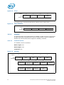
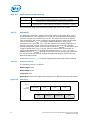
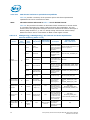
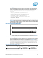
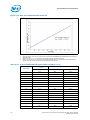
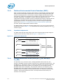
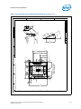
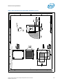
Figure 1-1 and Figure 1-2, shows the processor 2-socket and 4-socket platform
configuration. The “Legacy CPU” is the boot processor that is connected to the PCH
component, this socket is set to NodeID[0]. In the 4-socket configuration, the “Remote
CPU” is the processor which is not connected to the Legacy CPU.
Intel® Xeon® Processor E5-1600/E5-2600/E5-4600 Product Families
Datasheet Volume One
13
Overview
Figure 1-1.
Intel® Xeon® Processor E5-2600 Product Family on the 2 Socket
Platform
Figure 1-2.
Intel® Xeon® Processor E5-4600 Product Family on the 4 Socket
Platform
1.1.1
Processor Feature Details
• Up to 8 execution cores
• Each core supports two threads (Intel® Hyper-Threading Technology), up to 16
threads per socket
14
Intel® Xeon® Processor E5-1600/E5-2600/E5-4600 Product Families
Datasheet Volume One
Overview
• 46-bit physical addressing and 48-bit virtual addressing
• 1 GB large page support for server applications
• A 32-KB instruction and 32-KB data first-level cache (L1) for each core
• A 256-KB shared instruction/data mid-level (L2) cache for each core
• Up to 20 MB last level cache (LLC): up to 2.5 MB per core instruction/data last level
cache (LLC), shared among all cores
• The Intel® Xeon® processor E5-4600 product family supports Directory Mode,
Route Through, and Node IDs to reduce unnecessary Intel QuickPath Interconnect
traffic by tracking cache lines present in remote sockets.
1.1.2
Supported Technologies
• Intel® Virtualization Technology (Intel® VT)
• Intel® Virtualization Technology (Intel® VT) for Directed I/O (Intel® VT-d)
• Intel Virtualization Technology Processor Extensions
• Intel® Trusted Execution Technology (Intel® TXT)
• Intel® Advanced Encryption Standard Instructions (Intel® AES-NI)
• Intel 64 Architecture
• Intel® Streaming SIMD Extensions 4.1 (Intel SSE4.1)
• Intel Streaming SIMD Extensions 4.2 (Intel SSE4.2)
• Intel Advanced Vector Extensions (Intel AVX)
• Intel® Hyper-Threading Technology (Intel® HT Technology)
• Execute Disable Bit
• Intel® Turbo Boost Technology
• Intel® Intelligent Power Technology
• Enhanced Intel SpeedStep® Technology
• Intel® Dynamic Power Technology (Intel® DPT) (Memory Power Management)
1.2
Interfaces
1.2.1
System Memory Support
• Intel® Xeon® processor E5-1600/E5-2600/E5-4600 product families supports 4
DDR3 channels
• Unbuffered DDR3 and registered DDR3 DIMMs
• LR DIMM (Load Reduced DIMM) for buffered memory solutions demanding higher
capacity memory subsystems
• Independent channel mode or lockstep mode
• Data burst length of eight cycles for all memory organization modes
• Memory DDR3 data transfer rates of 800, 1066, 1333, and 1600 MT/s
• 64-bit wide channels plus 8-bits of ECC support for each channel
• DDR3 standard I/O Voltage of 1.5 V and DDR3 Low Voltage of 1.35 V
• 1-Gb, 2-Gb and 4-Gb DDR3 DRAM technologies supported for these devices:
Intel® Xeon® Processor E5-1600/E5-2600/E5-4600 Product Families
Datasheet Volume One
15
Overview
— UDIMMs x8, x16
— RDIMMs x4, x8
— LRDIMM x4, x8 (2-Gb and 4-Gb only)
• Up to 8 ranks supported per memory channel, 1, 2 or 4 ranks per DIMM
• Open with adaptive idle page close timer or closed page policy
• Per channel memory test and initialization engine can initialize DRAM to all logical
zeros with valid ECC (with or without data scrambler) or a predefined test pattern
• Isochronous access support for Quality of Service (QoS), native 1 and 2 socket
platforms - Intel® Xeon® processor E5-1600 and E5-2600 product families only
• Minimum memory configuration: independent channel support with 1 DIMM
populated
• Integrated dual SMBus master controllers
• Command launch modes of 1n/2n
• RAS Support (including and not limited to):
— Rank Level Sparing and Device Tagging
— Demand and Patrol Scrubbing
— DRAM Single Device Data Correction (SDDC) for any single x4 or x8 DRAM
device failure. Independent channel mode supports x4 SDDC. x8 SDDC
requires lockstep mode
— Lockstep mode where channels 0 & 1 and channels 2 & 3 are operated in
lockstep mode
— The combination of memory channel pair lockstep and memory mirroring is not
supported
— Data scrambling with address to ease detection of write errors to an incorrect
address.
— Error reporting via Machine Check Architecture
— Read Retry during CRC error handling checks by iMC
— Channel mirroring within a socket Channel Mirroring mode is supported on
memory channels 0 & 1 and channels 2 & 3
— Corrupt Data Containment
— MCA Recovery
• Improved Thermal Throttling with dynamic Closed Loop Thermal Throttling (CLTT)
• Memory thermal monitoring support for DIMM temperature via two memory
signals, MEM_HOT_C{01/23}_N
1.2.2
PCI Express*
• The PCI Express* port(s) are fully-compliant to the PCI Express* Base
Specification, Revision 3.0 (PCIe* 3.0)
• Support for PCI Express* 3.0 (8.0 GT/s), 2.0 (5.0 GT/s), and 1.0 (2.5 GT/s)
• Up to 40 lanes of PCI Express* interconnect for general purpose PCI Express*
devices at PCIe* 3.0 speeds that are configurable for up to 10 independent ports
• 4 lanes of PCI Express* at PCIe* 2.0 speeds when not using DMI2 port (Port 0),
also can be downgraded to x2 or x1
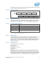
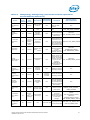
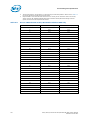
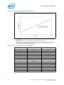
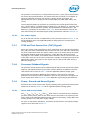
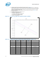
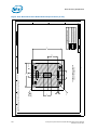
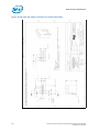
• Negotiating down to narrower widths is supported, see Figure 1-3:
16
Intel® Xeon® Processor E5-1600/E5-2600/E5-4600 Product Families
Datasheet Volume One
Overview
— x16 port (Port 2 & Port 3) may negotiate down to x8, x4, x2, or x1.
— x8 port (Port 1) may negotiate down to x4, x2, or x1.
— x4 port (Port 0) may negotiate down to x2, or x1.
— When negotiating down to narrower widths, there are caveats as to how lane
reversal is supported.
• Non-Transparent Bridge (NTB) is supported by PCIe* Port3a/IOU1. For more details
on NTB mode operation refer to PCI Express Base Specification - Revision 3.0:
— x4 or x8 widths and at PCIe* 1.0, 2.0, 3.0 speeds
— Two usage models; NTB attached to a Root Port or NTB attached to another
NTB
— Supports three 64-bit BARs
— Supports posted writes and non-posted memory read transactions across the
NTB
— Supports INTx, MSI and MSI-X mechanisms for interrupts on both side of NTB
in upstream direction only
• Address Translation Services (ATS) 1.0 support
• Hierarchical PCI-compliant configuration mechanism for downstream devices.
• Traditional PCI style traffic (asynchronous snooped, PCI ordering).
• PCI Express* extended configuration space. The first 256 bytes of configuration
space aliases directly to the PCI compatibility configuration space. The remaining
portion of the fixed 4-KB block of memory-mapped space above that (starting at
100h) is known as extended configuration space.
• PCI Express* Enhanced Access Mechanism. Accessing the device configuration
space in a flat memory mapped fashion.
• Automatic discovery, negotiation, and training of link out of reset.
• Supports receiving and decoding 64 bits of address from PCI Express*.
— Memory transactions received from PCI Express* that go above the top of
physical address space (when Intel VT-d is enabled, the check would be against
the translated HPA (Host Physical Address) address) are reported as errors by
the processor.
— Outbound access to PCI Express* will always have address bits 63 to 46
cleared.
• Re-issues Configuration cycles that have been previously completed with the
Configuration Retry status.
• Power Management Event (PME) functions.
• Message Signaled Interrupt (MSI and MSI-X) messages
• Degraded Mode support and Lane Reversal support
• Static lane numbering reversal and polarity inversion support
Intel® Xeon® Processor E5-1600/E5-2600/E5-4600 Product Families
Datasheet Volume One
17
Overview
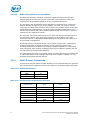
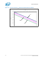
Figure 1-3.
PCI Express* Lane Partitioning and Direct Media Interface Gen 2 (DMI2)
Port 0
DMI / PCIe
Transaction
Link
Physical
Port 1
(IOU2)
PCIe
Port 2
(IOU0)
PCIe
Transaction
Port 3
(IOU1)
PCIe
Transaction
Link
Transaction
Link
Physical
Link
Physical
Physical
0…3
0…3
4…7
0…3
4…7
8…11
12..15
0…3
4…7
8…11
12..15
X4
X4
X4
X4
X4
X4
X4
X4
X4
X4
X4
DMI
Po rt 1a
Po rt 1b
Po rt 2a
Po rt 2b
Po rt 2c
Po rt 2d
Po rt 3a
Po rt 3b
Po rt 3c
Po rt 3d
X8
X8
X8
X8
X8
Po rt 1a
Po rt 2a
Po rt 2c
Po rt 3a
Po rt 3c
X16
Po rt 2a
1.2.3
X16
Po rt 3a
Direct Media Interface Gen 2 (DMI2)
• Serves as the chip-to-chip interface to the Intel® C600 Chipset
• The DMI2 port supports x4 link width and only operates in a x4 mode when in DMI2
• Operates at PCI Express* 1.0 or 2.0 speeds
• Transparent to software
• Processor and peer-to-peer writes and reads with 64-bit address support
• APIC and Message Signaled Interrupt (MSI) support. Will send Intel-defined “End of
Interrupt” broadcast message when initiated by the processor.
• System Management Interrupt (SMI), SCI, and SERR error indication
• Static lane numbering reversal support
• Supports DMI2 virtual channels VC0, VC1, VCm, and VCp
1.2.4
Intel® QuickPath Interconnect (Intel® QPI)
• Compliant with Intel QuickPath Interconnect v1.1 standard packet formats
• Implements two full width Intel QPI ports
• Full width port includes 20 data lanes and 1 clock lane
• 64 byte cache-lines
• Isochronous access support for Quality of Service (QoS), native 1 and 2 socket
platforms - Intel® Xeon® processor E5-1600 and E5-2600 product families only
18
Intel® Xeon® Processor E5-1600/E5-2600/E5-4600 Product Families
Datasheet Volume One
Overview
• Home snoop based coherency
• 3-bit Node ID
• 46-bit physical addressing support
• No Intel QuickPath Interconnect bifurcation support
• Differential signaling
• Forwarded clocking
• Up to 8.0 GT/s data rate (up to 16 GB/s direction peak bandwidth per port)
— All ports run at same operational frequency
— Reference Clock is 100 MHz
— Slow boot speed initialization at 50 MT/s
• Common reference clocking (same clock generator for both sender and receiver)
• Intel® Interconnect Built-In-Self-Test (Intel® IBIST) for high-speed testability
• Polarity and Lane reversal (Rx side only)
1.2.5
Platform Environment Control Interface (PECI)
The PECI is a one-wire interface that provides a communication channel between a
PECI client (the processor) and a PECI master (the PCH).
• Supports operation at up to 2 Mbps data transfers
• Link layer improvements to support additional services and higher efficiency over
PECI 2.0 generation
• Services include CPU thermal and estimated power information, control functions
for power limiting, P-state and T-state control, and access for Machine Check
Architecture registers and PCI configuration space (both within the processor
package and downstream devices)
• PECI address determined by SOCKET_ID configuration
• Single domain (Domain 0) is supported
1.3
Power Management Support
1.3.1
Processor Package and Core States
• ACPI C-states as implemented by the following processor C-states:
— Package: PC0, PC1/PC1E, PC2, PC3, PC6 (Package C7 is not supported)
— Core: CC0, CC1, CC1E, CC3, CC6, CC7
• Enhanced Intel SpeedStep® Technology
1.3.2
System States Support
• S0, S1, S3, S4, S5
1.3.3
Memory Controller
• Multiple CKE power down modes
• Multiple self-refresh modes
Intel® Xeon® Processor E5-1600/E5-2600/E5-4600 Product Families
Datasheet Volume One
19
Overview
• Memory thermal monitoring via MEM_HOT_C01_N and MEM_HOT_C23_N Signals
1.3.4
PCI Express
• L0s is not supported
• L1 ASPM power management capability
1.3.5
Intel QuickPath Interconnect
• L0s is not supported
• L0p and L1 power management capabilities
1.4
Thermal Management Support
• Digital Thermal Sensor with multiple on-die temperature zones
• Adaptive Thermal Monitor
• THERMTRIP_N and PROCHOT_N signal support
• On-Demand mode clock modulation
• Open and Closed Loop Thermal Throttling (OLTT/CLTT) support for system memory
in addition to Hybrid OLTT/CLTT mode
• Fan speed control with DTS
• Two integrated SMBus masters for accessing thermal data from DIMMs
• New Memory Thermal Throttling features via MEM_HOT_C{01/23}_N signals
• Running Average Power Limit (RAPL), Processor and DRAM Thermal and Power
Optimization Capabilities
1.5
Package Summary
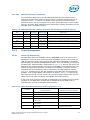
The processor socket is a 52.5 x 45 mm FCLGA package (LGA2011-0 land FCLGA10).
1.6
Terminology
Term
20
Description
ASPM
Active State Power Management
BMC
Baseboard Management Controllers
Cbo
Cache and Core Box. It is a term used for internal logic providing ring interface to
LLC and Core.
DDR3
Third generation Double Data Rate SDRAM memory technology that is the
successor to DDR2 SDRAM
DMA
Direct Memory Access
DMI
Direct Media Interface
DMI2
Direct Media Interface Gen 2
DTS
Digital Thermal Sensor
ECC
Error Correction Code
Intel® Xeon® Processor E5-1600/E5-2600/E5-4600 Product Families
Datasheet Volume One
Overview
Term
Description
Enhanced Intel
SpeedStep® Technology
Allows the operating system to reduce power consumption when performance is
not needed.
Execute Disable Bit
The Execute Disable bit allows memory to be marked as executable or nonexecutable, when combined with a supporting operating system. If code
attempts to run in non-executable memory the processor raises an error to the
operating system. This feature can prevent some classes of viruses or worms
that exploit buffer overrun vulnerabilities and can thus help improve the overall
security of the system. See the Intel® 64 and IA-32 Architectures Software
Developer's Manuals for more detailed information.
Flit
Flow Control Unit. The Intel QPI Link layer’s unit of transfer; 1 Flit = 80-bits.
Functional Operation
Refers to the normal operating conditions in which all processor specifications,
including DC, AC, system bus, signal quality, mechanical, and thermal, are
satisfied.
IMC
The Integrated Memory Controller. A Memory Controller that is integrated in the
processor die.
IIO
The Integrated I/O Controller. An I/O controller that is integrated in the
processor die.
Intel® ME
Intel® Management Engine (Intel® ME)
Intel® QuickData
Technology
Intel QuickData Technology is a platform solution designed to maximize the
throughput of server data traffic across a broader range of configurations and
server environments to achieve faster, scalable, and more reliable I/O.
Intel® QuickPath
Interconnect (Intel® QPI)
A cache-coherent, link-based Interconnect specification for Intel processors,
chipsets, and I/O bridge components.
Intel® 64 Technology
64-bit memory extensions to the IA-32 architecture. Further details on Intel 64
architecture and programming model can be found at
http://developer.intel.com/technology/intel64/.
Intel® Turbo Boost
Technology
Intel® Turbo Boost Technology is a way to automatically run the processor core
faster than the marked frequency if the part is operating under power,
temperature, and current specifications limits of the Thermal Design Power
(TDP). This results in increased performance of both single and multi-threaded
applications.
Intel® TXT
Intel® Trusted Execution Technology
Intel® Virtualization
Technology (Intel® VT)
Processor virtualization which when used in conjunction with Virtual Machine
Monitor software enables multiple, robust independent software environments
inside a single platform.
Intel® VT-d
Intel® Virtualization Technology (Intel® VT) for Directed I/O. Intel VT-d is a
hardware assist, under system software (Virtual Machine Manager or OS)
control, for enabling I/O device virtualization. Intel VT-d also brings robust
security by providing protection from errant DMAs by using DMA remapping, a
key feature of Intel VT-d.
Intel® Xeon® processor
E5-1600 product family
and Intel® Xeon®
processor E5-2600
product family
Intel’s 32-nm processor design, follow-on to the 32-nm 2nd Generation Intel®
Core™ Processor Family design. It is the first processor for use in Intel® Xeon®
processor E5-1600 and E5-2600 product families-based platforms. Intel®
Xeon® processor E5-1600 product family and Intel® Xeon® processor E5-2600
product family supports Efficient Performance server, workstation and HPC
platforms
Intel® Xeon® processor
E5-4600 product family
Intel’s 32-nm processor design, follow-on to the 32-nm processor design. It is
the first processor for use in Intel® Xeon® processor E5-4600 product familybased platforms. Intel® Xeon® processor E5-4600 product family supports
scalable server and HPC platforms for two or more processors, including glueless
four-way platforms.
Integrated Heat Spreader
(IHS)
A component of the processor package used to enhance the thermal
performance of the package. Component thermal solutions interface with the
processor at the IHS surface.
Jitter
Any timing variation of a transition edge or edges from the defined Unit Interval
(UI).
IOV
I/O Virtualization
LGA2011-0 land FCLGA10
Socket
The processor mates with the system board through this surface mount,
LGA2011-0 land FCLGA10 contact socket, for the Intel® Xeon® processor E5
product family-based platform.
Intel® Xeon® Processor E5-1600/E5-2600/E5-4600 Product Families
Datasheet Volume One
21
Overview
Term
22
Description
LLC
Last Level Cache
LRDIMM
Load Reduced Dual In-line Memory Module
NCTF
Non-Critical to Function: NCTF locations are typically redundant ground or noncritical reserved, so the loss of the solder joint continuity at end of life conditions
will not affect the overall product functionality.
NEBS
Network Equipment Building System. NEBS is the most common set of
environmental design guidelines applied to telecommunications equipment in the
United States.
PCH
Platform Controller Hub (Intel® C600 Chipset). The next generation chipset with
centralized platform capabilities including the main I/O interfaces along with
display connectivity, audio features, power management, manageability, security
and storage features.
PCU
Power Control Unit
PCI Express* 3.0
The third generation PCI Express* specification that operates at twice the speed
of PCI Express* 2.0 (8 Gb/s); however, PCI Express* 3.0 is completely backward
compatible with PCI Express* 1.0 and 2.0.
PCI Express* 3
PCI Express* Generation 3.0
PCI Express* 2
PCI Express* Generation 2.0
PCI Express*
PCI Express* Generation 2.0/3.0
PECI
Platform Environment Control Interface
Phit
Physical Unit. An Intel® QPI terminology defining units of transfer at the physical
layer. 1 Phit is equal to 20 bits in ‘full width mode’ and 10 bits in ‘half width
mode’
Processor
The 64-bit, single-core or multi-core component (package)
Processor Core
The term “processor core” refers to silicon die itself which can contain multiple
execution cores. Each execution core has an instruction cache, data cache, and
256-KB L2 cache. All execution cores share the L3 cache. All DC and signal
integrity specifications are measured at the processor die (pads), unless
otherwise noted.
RDIMM
Registered Dual In-line Memory Module
Rank
A unit of DRAM corresponding four to eight devices in parallel, ignoring ECC.
These devices are usually, but not always, mounted on a single side of a DDR3
DIMM.
Scalable-2S
Intel® Xeon® processor E5 product family-based platform targeted for scalable
designs using third party Node Controller chip. In these designs, Node Controller
is used to scale the design beyond one/two/four sockets.
SCI
System Control Interrupt. Used in ACPI protocol.
SSE
Intel® Streaming SIMD Extensions (Intel® SSE)
SKU
A processor Stock Keeping Unit (SKU) to be installed in either server or
workstation platforms. Electrical, power and thermal specifications for these
SKU’s are based on specific use condition assumptions. Server processors may
be further categorized as Efficient Performance server, workstation and HPC
SKUs. For further details on use condition assumptions, please refer to the latest
Product Release Qualification (PRQ) Report available via your Customer Quality
Engineer (CQE) contact.
SMBus
System Management Bus. A two-wire interface through which simple system and
power management related devices can communicate with the rest of the
system. It is based on the principals of the operation of the I2C* two-wire serial
bus from Philips Semiconductor.
Storage Conditions
A non-operational state. The processor may be installed in a platform, in a tray,
or loose. Processors may be sealed in packaging or exposed to free air. Under
these conditions, processor landings should not be connected to any supply
voltages, have any I/Os biased or receive any clocks. Upon exposure to “free air”
(i.e., unsealed packaging or a device removed from packaging material) the
processor must be handled in accordance with moisture sensitivity labeling
(MSL) as indicated on the packaging material.
TAC
Thermal Averaging Constant
Intel® Xeon® Processor E5-1600/E5-2600/E5-4600 Product Families
Datasheet Volume One
Overview
Term
1.7
Description
TDP
Thermal Design Power
TSOD
Thermal Sensor on DIMM
UDIMM
Unbuffered Dual In-line Module
Uncore
The portion of the processor comprising the shared cache, IMC, HA, PCU, UBox,
and Intel QPI link interface.
Unit Interval
Signaling convention that is binary and unidirectional. In this binary signaling,
one bit is sent for every edge of the forwarded clock, whether it be a rising edge
or a falling edge. If a number of edges are collected at instances t1, t2, tn,...., tk
then the UI at instance “n” is defined as:
UI n = t n - t n - 1
VCC
Processor core power supply
VSS
Processor ground
VCCD_01, VCCD_23
Variable power supply for the processor system memory interface. VCCD is the
generic term for VCCD_01, VCCD_23.
x1
Refers to a Link or Port with one Physical Lane
x4
Refers to a Link or Port with four Physical Lanes
x8
Refers to a Link or Port with eight Physical Lanes
x16
Refers to a Link or Port with sixteen Physical Lanes
Related Documents
Refer to the following documents for additional information.
Table 1-1.
Referenced Documents (Sheet 1 of 2)
Document
Location
Intel® Xeon® Processor E5 Product Family Datasheet Volume Two
http://www.intel.com
Intel® Xeon® Processor E5-1600/E5-2600/E5-4600 Product Families
Thermal/Mechanical Design Guide
http://www.intel.com
Intel® Xeon® Processor E5-1600/E5-2600/E5-4600 Product Families
– BSDL (Boundary Scan Description Language)
http://www.intel.com
Intel® C600 Series Chipset Data Sheet
http://www.intel.com
Intel® 64 and IA-32 Architectures Software Developer’s Manual
(SDM) Volumes 1, 2, and 3
http://www.intel.com
Advanced Configuration and Power Interface Specification 3.0
http://www.acpi.info
PCI Local Bus Specification 3.0
http://www.pcisig.com/specifications
PCI Express Base Specification - Revision 2.1 and 1.1
PCI Express Base Specification - Revision 3.0
http://www.pcisig.com
System Management Bus (SMBus) Specification
http://smbus.org/
DDR3 SDRAM Specification
http://www.jedec.org
Low (JESD22-A119) and High (JESD-A103) Temperature Storage Life
Specifications
http://www.jedec.org
Intel 64 and IA-32 Architectures Software Developer's Manuals
• Volume 1: Basic Architecture
• Volume 2A: Instruction Set Reference, A-M
• Volume 2B: Instruction Set Reference, N-Z
• Volume 3A: System Programming Guide
• Volume 3B: System Programming Guide
Intel® 64 and IA-32 Architectures Optimization Reference Manual
Intel® Xeon® Processor E5-1600/E5-2600/E5-4600 Product Families
Datasheet Volume One
http://www.intel.com/products/proce
ssor/manuals/index.htm
23
Overview
Table 1-1.
Referenced Documents (Sheet 2 of 2)
Document
1.8
Location
Intel® Virtualization Technology Specification for Directed I/O
Architecture Specification
http://download.intel.com/technolog
y/computing/vptech/Intel(r)_VT_for_
Direct_IO.pdf
Intel® Trusted Execution Technology Software Development Guide
http://www.intel.com/technology/sec
urity/
State of Data
The data contained within this document is the most accurate information available by
the publication date of this document.
§
24
Intel® Xeon® Processor E5-1600/E5-2600/E5-4600 Product Families
Datasheet Volume One
Interfaces
2
Interfaces
This chapter describes the interfaces supported by the processor.
2.1
System Memory Interface
2.1.1
System Memory Technology Support
The Integrated Memory Controller (IMC) supports DDR3 protocols with four
independent 64-bit memory channels with 8 bits of ECC for each channel (total of
72-bits) and supports 1 to 3 DIMMs per channel depending on the type of memory
installed. The type of memory supported by the processor is dependent on the target
platform:
• Intel® Xeon® processor E5 product family-based platforms support:
— ECC registered DIMMs: with a maximum of three DIMMs per channel allowing
up to eight device ranks per channel.
— ECC and non-ECC unbuffered DIMMs: with a maximum of two DIMMs per
channel thus allowing up to four device ranks per channel. Support for mixed
non-ECC with ECC un-buffered DIMM configurations.
2.1.2
System Memory Timing Support
The IMC supports the following DDR3 Speed Bin, CAS Write Latency (CWL), and
command signal mode timings on the main memory interface:
• tCL = CAS Latency
• tRCD = Activate Command to READ or WRITE Command delay
• tRP = PRECHARGE Command Period
• CWL = CAS Write Latency
• Command Signal modes = 1n indicates a new command may be issued every clock
and 2n indicates a new command may be issued every 2 clocks. Command launch
mode programming depends on the transfer rate and memory configuration.
Intel® Xeon® Processor E5-1600/E5-2600/E5-4600 Product Families
Datasheet Volume One
25
Interfaces
2.2
PCI Express* Interface
This section describes the PCI Express* 3.0 interface capabilities of the processor. See
the PCI Express* Base Specification for details of PCI Express* 3.0.
2.2.1
PCI Express* Architecture
Compatibility with the PCI addressing model is maintained to ensure that all existing
applications and drivers operate unchanged. The PCI Express* configuration uses
standard mechanisms as defined in the PCI Plug-and-Play specification.
The PCI Express* architecture is specified in three layers: Transaction Layer, Data Link
Layer, and Physical Layer. The partitioning in the component is not necessarily along
these same boundaries. Refer to Figure 2-1 for the PCI Express* Layering Diagram.
Figure 2-1.
PCI Express* Layering Diagram
Transaction
Transaction
Data Link
Data Link
Physical
Physical
Logical Sub-Block
Logical Sub-Block
Electrical Sub-Block
Electrical Sub-Block
RX
TX
RX
TX
PCI Express* uses packets to communicate information between components. Packets
are formed in the Transaction and Data Link Layers to carry the information from the
transmitting component to the receiving component. As the transmitted packets flow
through the other layers, they are extended with additional information necessary to
handle packets at those layers. At the receiving side, the reverse process occurs and
packets get transformed from their Physical Layer representation to the Data Link
Layer representation and finally (for Transaction Layer Packets) to the form that can be
processed by the Transaction Layer of the receiving device.
26
Intel® Xeon® Processor E5-1600/E5-2600/E5-4600 Product Families
Datasheet Volume One
Interfaces
Figure 2-2.
Packet Flow through the Layers
Framing
Sequence
Number
Header
Data
ECRC
LCRC
Framing
Transaction Layer
Data Link Layer
Physical Layer
2.2.1.1
Transaction Layer
The upper layer of the PCI Express* architecture is the Transaction Layer. The
Transaction Layer's primary responsibility is the assembly and disassembly of
Transaction Layer Packets (TLPs). TLPs are used to communicate transactions, such as
read and write, as well as certain types of events. The Transaction Layer also manages
flow control of TLPs.
2.2.1.2
Data Link Layer
The middle layer in the PCI Express* stack, the Data Link Layer, serves as an
intermediate stage between the Transaction Layer and the Physical Layer.
Responsibilities of Data Link Layer include link management, error detection, and error
correction.
The transmission side of the Data Link Layer accepts TLPs assembled by the
Transaction Layer, calculates and applies data protection code and TLP sequence
number, and submits them to Physical Layer for transmission across the Link. The
receiving Data Link Layer is responsible for checking the integrity of received TLPs and
for submitting them to the Transaction Layer for further processing. On detection of TLP
error(s), this layer is responsible for requesting retransmission of TLPs until information
is correctly received, or the Link is determined to have failed. The Data Link Layer also
generates and consumes packets which are used for Link management functions.
2.2.1.3
Physical Layer
The Physical Layer includes all circuitry for interface operation, including driver and
input buffers, parallel-to-serial and serial-to-parallel conversion, PLL(s), and impedance
matching circuitry. It also includes logical functions related to interface initialization and
maintenance. The Physical Layer exchanges data with the Data Link Layer in an
implementation-specific format, and is responsible for converting this to an appropriate
serialized format and transmitting it across the PCI Express* Link at a frequency and
width compatible with the remote device.
2.2.2
PCI Express* Configuration Mechanism
The PCI Express* link is mapped through a PCI-to-PCI bridge structure.
PCI Express* extends the configuration space to 4096 bytes per-device/function, as
compared to 256 bytes allowed by the Conventional PCI Specification. PCI Express*
configuration space is divided into a PCI-compatible region (which consists of the first
Intel® Xeon® Processor E5-1600/E5-2600/E5-4600 Product Families
Datasheet Volume One
27
Interfaces
256 bytes of a logical device's configuration space) and an extended PCI Express*
region (which consists of the remaining configuration space). The PCI-compatible
region can be accessed using either the mechanisms defined in the PCI specification or
using the enhanced PCI Express* configuration access mechanism described in the PCI
Express* Enhanced Configuration Mechanism section.
The PCI Express* Host Bridge is required to translate the memory-mapped PCI
Express* configuration space accesses from the host processor to PCI Express*
configuration cycles. To maintain compatibility with PCI configuration addressing
mechanisms, it is recommended that system software access the enhanced
configuration space using 32-bit operations (32-bit aligned) only.
See the PCI Express* Base Specification for details of both the PCI-compatible and PCI
Express* Enhanced configuration mechanisms and transaction rules.
2.3
DMI2/PCI Express* Interface
Direct Media Interface 2 (DMI2) connects the processor to the Platform Controller Hub
(PCH). DMI2 is similar to a four-lane PCI Express* supporting a speed of 5 GT/s per
lane. This interface can be configured at power-on to serve as a x4 PCI Express* link
based on the setting of the SOCKET_ID[1:0] and FRMAGENT signal for processors not
connected to a PCH.
Note:
Only DMI2 x4 configuration is supported.
2.3.1
DMI2 Error Flow
DMI2 can only generate SERR in response to errors, never SCI, SMI, MSI, PCI INT, or
GPE. Any DMI2 related SERR activity is associated with Device 0.
2.3.2
Processor/PCH Compatibility Assumptions
The processor is compatible with the PCH and is not compatible with any previous MCH
or ICH products.
2.3.3
DMI2 Link Down
The DMI2 link going down is a fatal, unrecoverable error. If the DMI2 data link goes to
data link down, after the link was up, then the DMI2 link hangs the system by not
allowing the link to retrain to prevent data corruption. This is controlled by the PCH.
Downstream transactions that had been successfully transmitted across the link prior
to the link going down may be processed as normal. No completions from downstream,
non-posted transactions are returned upstream over the DMI2 link after a link down
event.
2.4
Intel QuickPath Interconnect
The Intel QuickPath Interconnect is a high speed, packetized, point-to-point
interconnect used in the 2nd Generation Intel(r) Core(TM) Processor Family. The
narrow high-speed links stitch together processors in distributed shared memory and
integrated I/O platform architecture. It offers much higher bandwidth with low latency.
The Intel QuickPath Interconnect has an efficient architecture allowing more
interconnect performance to be achieved in real systems. It has a snoop protocol
28
Intel® Xeon® Processor E5-1600/E5-2600/E5-4600 Product Families
Datasheet Volume One
Interfaces
optimized for low latency and high scalability, as well as packet and lane structures
enabling quick completions of transactions. Reliability, availability, and serviceability
features (RAS) are built into the architecture.
The physical connectivity of each interconnect link is made up of twenty differential
signal pairs plus a differential forwarded clock. Each port supports a link pair consisting
of two uni-directional links to complete the connection between two components. This
supports traffic in both directions simultaneously. To facilitate flexibility and longevity,
the interconnect is defined as having five layers: Physical, Link, Routing, Transport, and
Protocol.
• The Physical layer consists of the actual wires carrying the signals, as well as
circuitry and logic to support ancillary features required in the transmission and
receipt of the 1s and 0s. The unit of transfer at the Physical layer is 20-bits, which
is called a Phit (for Physical unit).
• The Link layer is responsible for reliable transmission and flow control. The Link
layer’s unit of transfer is 80-bits, which is called a Flit (for Flow control unit).
• The Routing layer provides the framework for directing packets through the
fabric.
• The Transport layer is an architecturally defined layer (not implemented in the
initial products) providing advanced routing capability for reliable end-to-end
transmission.
• The Protocol layer is the high-level set of rules for exchanging packets of data
between devices. A packet is comprised of an integral number of Flits.
The Intel QuickPath Interconnect includes a cache coherency protocol to keep the
distributed memory and caching structures coherent during system operation. It
supports both low-latency source snooping and a scalable home snoop behavior. The
coherency protocol provides for direct cache-to-cache transfers for optimal latency.
Intel® Xeon® Processor E5-1600/E5-2600/E5-4600 Product Families
Datasheet Volume One
29
2.5
Platform Environment Control Interface (PECI)
The Platform Environment Control Interface (PECI) uses a single wire for self-clocking
and data transfer. The bus requires no additional control lines. The physical layer is a
self-clocked one-wire bus that begins each bit with a driven, rising edge from an idle
level near zero volts. The duration of the signal driven high depends on whether the bit
value is a logic ‘0’ or logic ‘1’. PECI also includes variable data transfer rate established
with every message. In this way, it is highly flexible even though underlying logic is
simple.
The interface design was optimized for interfacing to Intel processor and chipset
components in both single processor and multiple processor environments. The single
wire interface provides low board routing overhead for the multiple load connections in
the congested routing area near the processor and chipset components. Bus speed,
error checking, and low protocol overhead provides adequate link bandwidth and
reliability to transfer critical device operating conditions and configuration information.
The PECI bus offers:
• A wide speed range from 2 Kbps to 2 Mbps
• CRC check byte used to efficiently and atomically confirm accurate data delivery
• Synchronization at the beginning of every message minimizes device timing
accuracy requirements
Note:
The PECI commands described in this document apply primarily to the Intel® Xeon®
processor E5-1600/E5-2600/E5-4600 product families. The processors utilizes the
capabilities described in this document to indicate support for four memory channels.
Refer to Table 2-1 for the list of PECI commands supported by the processors.
Table 2-1.
Summary of Processor-specific PECI Commands
2.5.1
Command
Supported on the Processor
Ping()
Yes
GetDIB()
Yes
GetTemp()
Yes
RdPkgConfig()
Yes
WrPkgConfig()
Yes
RdIAMSR()
Yes
WrIAMSR()
No
RdPCIConfig()
Yes
WrPCIConfig()
No
RdPCIConfigLocal()
Yes
WrPCIConfigLocal()
Yes
PECI Client Capabilities
The processor PECI client is designed to support the following sideband functions:
• Processor and DRAM thermal management
• Platform manageability functions including thermal, power, and error monitoring
— The platform ‘power’ management includes monitoring and control for both the
processor and DRAM subsystem to assist with data center power limiting.
• Processor interface tuning and diagnostics capabilities (Intel® Interconnect BIST).
30
Intel® Xeon® Processor E5-1600/E5-2600/E5-4600 Product Families
Datasheet Volume One
2.5.1.1
Thermal Management
Processor fan speed control is managed by comparing Digital Thermal Sensor (DTS)
thermal readings acquired via PECI against the processor-specific fan speed control
reference point, or TCONTROL. Both TCONTROL and DTS thermal readings are accessible
via the processor PECI client. These variables are referenced to a common
temperature, the TCC activation point, and are both defined as negative offsets from
that reference.
PECI-based access to the processor package configuration space provides a means for
Baseboard Management Controllers (BMCs) or other platform management devices to
actively manage the processor and memory power and thermal features. Details on the
list of available power and thermal optimization services can be found in
Section 2.5.2.6.
2.5.1.2
Platform Manageability
PECI allows read access to certain error registers in the processor MSR space and
status monitoring registers in the PCI configuration space within the processor and
downstream devices. Details are covered in subsequent sections.
PECI permits writes to certain Memory Controller RAS-related registers in the processor
PCI configuration space. Details are covered in Section 2.5.2.10.
2.5.1.3
Processor Interface Tuning and Diagnostics
The processor Intel® Interconnect Built In Self Test (Intel® IBIST) allows for in-field
diagnostic capabilities in the Intel® QPI and memory controller interfaces. PECI
provides a port to execute these diagnostics via its PCI Configuration read and write
capabilities in the BMC INIT mode. Refer to Section 2.5.3.7 for more details.
2.5.2
Client Command Suite
PECI command requires at least one frame check sequence (FCS) byte to ensure
reliable data exchange between originator and client. The PECI message protocol
defines two FCS bytes that are returned by the client to the message originator. The
first FCS byte covers the client address byte, the Read and Write Length bytes, and all
bytes in the write data block. The second FCS byte covers the read response data
returned by the PECI client. The FCS byte is the result of a cyclic redundancy check
(CRC) of each data block.
2.5.2.1
Ping()
Ping() is a required message for all PECI devices. This message is used to enumerate
devices or determine if a device has been removed, been powered-off, etc. A Ping()
sent to a device address always returns a non-zero Write FCS if the device at the
targeted address is able to respond.
2.5.2.1.1
Command Format
The Ping() format is as follows:
Write Length: 0x00
Read Length: 0x00
Intel® Xeon® Processor E5-1600/E5-2600/E5-4600 Product Families
Datasheet Volume One
31
Figure 2-3.
Ping()
Byte #
Byte
Definition
0
1
2
3
Client Address
Write Length
0x00
Read Length
0x00
FCS
An example Ping() command to PECI device address 0x30 is shown below.
Figure 2-4.
Ping() Example
Byte #
Byte
Definition
2.5.2.2
0
1
2
3
0x30
0x00
0x00
0xe1
GetDIB()
The processor PECI client implementation of GetDIB() includes an 8-byte response and
provides information regarding client revision number and the number of supported
domains. All processor PECI clients support the GetDIB() command.
2.5.2.2.1
Command Format
The GetDIB() format is as follows:
Write Length: 0x01
Read Length: 0x08
Command: 0xf7
Figure 2-5.
GetDIB()
Byte #
Byte
Definition
32
0
1
2
3
4
Client Address
Write Length
0x01
Read Length
0x08
Cmd Code
0xf7
FCS
5
6
7
8
9
Device Info
Revision
Number
Reserved
Reserved
Reserved
10
11
12
13
Reserved
Reserved
Reserved
FCS
Intel® Xeon® Processor E5-1600/E5-2600/E5-4600 Product Families
Datasheet Volume One
2.5.2.2.2
Device Info
The Device Info byte gives details regarding the PECI client configuration. At a
minimum, all clients supporting GetDIB will return the number of domains inside the
package via this field. With any client, at least one domain (Domain 0) must exist.
Therefore, the Number of Domains reported is defined as the number of domains in
addition to Domain 0. For example, if bit 2 of the Device Info byte returns a ‘1’, that
would indicate that the PECI client supports two domains.
Figure 2-6.
Device Info Field Definition
Byte# 5
7 6 5 4 3 2 1 0
Reserved
# of Domains
Reserved
2.5.2.2.3
Revision Number
All clients that support the GetDIB command also support Revision Number reporting.
The revision number may be used by a host or originator to manage different command
suites or response codes from the client. Revision Number is always reported in the
second byte of the GetDIB() response. The ‘Major Revision’ number in Figure 2-7
always maps to the revision number of the PECI specification that the PECI client
processor is designed to. The ‘Minor Revision’ number value depends on the exact
command suite supported by the PECI client as defined in Table 2-2.
Figure 2-7.
Revision Number Definition
Byte# 6
7
4
3
0
Major Revision#
Minor Revision#
Table 2-2.
Minor Revision Number Meaning
Minor Revision
Supported Command Suite
0
Ping(), GetDIB(), GetTemp()
1
Ping(), GetDIB(), GetTemp(), WrPkgConfig(), RdPkgConfig()
2
Ping(), GetDIB(), GetTemp(), WrPkgConfig(), RdPkgConfig(), RdIAMSR()
3
Ping(), GetDIB(), GetTemp(), WrPkgConfig(), RdPkgConfig(), RdIAMSR(),
RdPCIConfigLocal(), WrPCIConfigLocal()
4
Ping(), GetDIB(), GetTemp(), WrPkgConfig(), RdPkgConfig(), RdIAMSR(),
RdPCIConfigLocal(), WrPCIConfigLocal(), RdPCIConfig()
Intel® Xeon® Processor E5-1600/E5-2600/E5-4600 Product Families
Datasheet Volume One
33
Table 2-2.
Minor Revision Number Meaning
Minor Revision
Supported Command Suite
5
Ping(), GetDIB(), GetTemp(), WrPkgConfig(), RdPkgConfig(), RdIAMSR(),
RdPCIConfigLocal(), WrPCIConfigLocal(), RdPCIConfig(), WrPCIConfig()
6
Ping(), GetDIB(), GetTemp(), WrPkgConfig(), RdPkgConfig(), RdIAMSR(),
RdPCIConfigLocal(), WrPCIConfigLocal(), RdPCIConfig(), WrPCIConfig(), WrIAMSR()
For the processor PECI client the Revision Number will return ‘0011 0100b’.
2.5.2.3
GetTemp()
The GetTemp() command is used to retrieve the maximum die temperature from a
target PECI address. The temperature is used by the external thermal management
system to regulate the temperature on the die. The data is returned as a negative
value representing the number of degrees centigrade below the maximum processor
junction temperature (Tjmax). The maximum PECI temperature value of zero
corresponds to the processor Tjmax. This also represents the default temperature at
which the processor Thermal Control Circuit activates. The actual value that the
thermal management system uses as a control set point (TCONTROL) is also defined as a
negative number below Tjmax. TCONTROL may be extracted from the processor by
issuing a PECI RdPkgConfig() command as described in Section 2.5.2.4 or using a
RDMSR instruction. TCONTROL application to fan speed control management is defined in
the Intel® Xeon® Processor E5-1600/E5-2600/E5-4600 Product Families Thermal/
Mechanical Design Guide.
Please refer to Section 2.5.7 for details regarding PECI temperature data formatting.
2.5.2.3.1
Command Format
The GetTemp() format is as follows:
Write Length: 0x01
Read Length: 0x02
Command: 0x01
Description: Returns the highest die temperature for addressed processor PECI client.
Figure 2-8.
GetTemp()
Byte #
Byte
Definition
34
0
1
2
3
Client Address
Write Length
0x01
Read Length
0x02
Cmd Code
0x01
4
5
6
7
FCS
Temp[7:0]
Temp[15:8]
FCS
Intel® Xeon® Processor E5-1600/E5-2600/E5-4600 Product Families
Datasheet Volume One
Example bus transaction for a thermal sensor device located at address 0x30 returning
a value of negative 10 counts is show in Figure 2-9.
Figure 2-9.
GetTemp() Example
Byte #
Byte
Definition
2.5.2.3.2
0
1
2
3
0x30
0x01
0x02
0x01
4
5
6
7
0xef
0x80
0xfd
0x4b
Supported Responses
The typical client response is a passing FCS and valid thermal data. Under some
conditions, the client’s response will indicate a failure. GetTemp() response definitions
are listed in Table 2-3. Refer to Section 2.5.7.4 for more details on sensor errors.
Table 2-3.
GetTemp() Response Definition
Response
General Sensor Error (GSE)1
Meaning
Thermal scan did not complete in time. Retry is appropriate.
Bad Write FCS
Electrical error
Abort FCS
Illegal command formatting (mismatched RL/WL/Command Code)
0x00001
Processor is running at its maximum temperature or is currently being reset.
All other data
Valid temperature reading, reported as a negative offset from the processor
Tjmax.
Notes:
1.
This response will be reflected in Bytes 5 & 6 in Figure 2-9.
2.5.2.4
RdPkgConfig()
The RdPkgConfig() command provides read access to the package configuration space
(PCS) within the processor, including various power and thermal management
functions. Typical PCS read services supported by the processor may include access to
temperature data, energy status, run time information, DIMM temperatures and so on.
Refer to Section 2.5.2.6 for more details on processor-specific services supported
through this command.
2.5.2.4.1
Command Format
The RdPkgConfig() format is as follows:
Write Length: 0x05
Read Length: 0x05 (dword)
Command: 0xa1
Description: Returns the data maintained in the processor package configuration
space for the PCS entry as specified by the ‘index’ and ‘parameter’ fields. The ‘index’
field contains the encoding for the requested service and is used in conjunction with the
‘parameter’ field to specify the exact data being requested. The Read Length dictates
the desired data return size. This command supports only dword responses on the
Intel® Xeon® Processor E5-1600/E5-2600/E5-4600 Product Families
Datasheet Volume One
35
processor PECI clients. All command responses are prepended with a completion code
that contains additional pass/fail status information. Refer to Section 2.5.5.2 for details
regarding completion codes.
Figure 2-10. RdPkgConfig()
Note:
The 2-byte parameter field and 4-byte read data field defined in Figure 2-10 are sent in standard PECI ordering with LSB
first and MSB last.
2.5.2.4.2
Supported Responses
The typical client response is a passing FCS, a passing Completion Code and valid data.
Under some conditions, the client’s response will indicate a failure.
Table 2-4.
RdPkgConfig() Response Definition
Response
Bad Write FCS
2.5.2.5
Meaning
Electrical error
Abort FCS
Illegal command formatting (mismatched RL/WL/Command Code)
CC: 0x40
Command passed, data is valid.
CC: 0x80
Response timeout. The processor is not able to generate the required response in a timely
fashion. Retry is appropriate.
CC: 0x81
Response timeout. The processor is not able to allocate resources for servicing this
command at this time. Retry is appropriate.
CC: 0x90
Unknown/Invalid/Illegal Request
CC: 0x91
PECI control hardware, firmware or associated logic error. The processor is unable to
process the request.
WrPkgConfig()
The WrPkgConfig() command provides write access to the package configuration space
(PCS) within the processor, including various power and thermal management
functions. Typical PCS write services supported by the processor may include power
limiting, thermal averaging constant programming and so on. Refer to Section 2.5.2.6
for more details on processor-specific services supported through this command.
2.5.2.5.1
Command Format
The WrPkgConfig() format is as follows:
Write Length: 0x0a(dword)
36
Intel® Xeon® Processor E5-1600/E5-2600/E5-4600 Product Families
Datasheet Volume One
Read Length: 0x01
Command: 0xa5
AW FCS Support: Yes
Description: Writes data to the processor PCS entry as specified by the ‘index’ and
‘parameter’ fields. This command supports only dword data writes on the processor
PECI clients. All command responses include a completion code that provides additional
pass/fail status information. Refer to Section 2.5.5.2 for details regarding completion
codes.
The Assured Write FCS (AW FCS) support provides the processor client a high degree of
confidence that the data it received from the host is correct. This is especially critical
where the consumption of bad data might result in improper or non-recoverable
operation.
Figure 2-11. WrPkgConfig()
Note:
2.5.2.5.2
The 2-byte parameter field and 4-byte write data field defined in Figure 2-11 are sent in standard PECI
ordering with LSB first and MSB last.
Supported Responses
The typical client response is a passing FCS, a passing Completion Code and valid data.
Under some conditions, the client’s response will indicate a failure.
Table 2-5.
WrPkgConfig() Response Definition (Sheet 1 of 2)
Response
Bad Write FCS
Meaning
Electrical error or AW FCS failure
Abort FCS
Illegal command formatting (mismatched RL/WL/Command Code)
CC: 0x40
Command passed, data is valid.
Intel® Xeon® Processor E5-1600/E5-2600/E5-4600 Product Families
Datasheet Volume One
37
Table 2-5.
WrPkgConfig() Response Definition (Sheet 2 of 2)
Response
2.5.2.6
Meaning
CC: 0x80
Response timeout. The processor was not able to generate the required response in a
timely fashion. Retry is appropriate.
CC: 0x81
Response timeout. The processor is not able to allocate resources for servicing this
command at this time. Retry is appropriate.
CC: 0x90
Unknown/Invalid/Illegal Request
CC: 0x91
PECI control hardware, firmware or associated logic error. The processor is unable to
process the request.
Package Configuration Capabilities
Table 2-6 combines both read and write services. Any service listed as a “read” would
use the RdPkgConfig() command and a service listed as a “write” would use the
WrPkgConfig() command. PECI requests for memory temperature or other data
generated outside the processor package do not trigger special polling cycles on the
processor memory or SMBus interfaces to procure the required information.
2.5.2.6.1
DRAM Thermal and Power Optimization Capabilities
DRAM thermal and power optimization (also known as RAPL or “Running Average
Power Limit”) services provide a way for platform thermal management solutions to
program and access DRAM power, energy and temperature parameters. Memory
temperature information is typically used to regulate fan speeds, tune refresh rates and
throttle the memory subsystem as appropriate. Memory temperature data may be
derived from a variety of sources including on-die or on-board DIMM sensors, DRAM
activity information or a combination of the two. Though memory temperature data is a
byte long, range of actual temperature values are determined by the DIMM
specifications and operating range.
Note:
DRAM related PECI services described in this section apply only to the memory
connected to the specific processor PECI client in question and not the overall platform
memory in general. For estimating DRAM thermal information in closed loop throttling
mode, a dedicated SMBus is required between the CPU and the DIMMs. The processor
PCU requires access to the VR12 voltage regulator for reading average output current
information through the SVID bus for initial DRAM RAPL related power tuning.
Table 2-6 provides a summary of the DRAM power and thermal optimization capabilities
that can be accessed over PECI on the processor. The Index values referenced in
Table 2-6 are in decimal format.
Table 2-6 also provides information on alternate inband mechanisms to access similar
or equivalent information through register reads and writes where applicable. The user
should consult the Intel® 64 and IA-32 Architectures Software Developer’s Manual
(SDM) Volumes 1, 2, and 3 or Intel® Xeon® Processor E5 Product Family Datasheet
Volume Two for details on MSR and CSR register contents.
38
Intel® Xeon® Processor E5-1600/E5-2600/E5-4600 Product Families
Datasheet Volume One
Table 2-6.
Service
DRAM Rank
Temperature
Write
DIMM
Temperature
Read
DIMM Ambient
Temperature
Write / Read
DIMM Ambient
Temperature
Write / Read
DRAM Channel
Temperature
Read
RdPkgConfig() & WrPkgConfig() DRAM Thermal and Power Optimization
Services Summary (Sheet 1 of 2)
Index
Value
(decimal)
Parameter
Value
(word)
RdPkgConfig()
Data
(dword)
WrPkgConfig()
Data
(dword)
Description
Alternate Inband
MSR or CSR
Access
18
Channel
Index &
DIMM Index
N/A
Absolute
temperature in
Degrees Celsius
for ranks 0, 1, 2
&3
Write
temperature for
each rank within
a single DIMM.
N/A
14
Channel
Index
Absolute
temperature in
Degrees Celsius for
DIMMs 0, 1, & 2
N/A
Read
temperature of
each DIMM
within a
channel.
CSR:
DIMMTEMPSTAT_[0:2]
0x0000
N/A
Absolute
temperature in
Degrees C to be
used as ambient
temperature
reference
Write ambient
temperature
reference for
activity-based
rank
temperature
estimation.
N/A
19
0x0000
Absolute
temperature in
Degrees C to be
used as ambient
temperature
reference
N/A
Read ambient
temperature
reference for
activity-based
rank
temperature
estimation.
N/A
22
0x0000
Maximum of all rank
temperatures for
each channel in
Degrees Celsius
N/A
Read the
maximum DRAM
channel
temperature.
N/A
N/A
Read the DRAM
energy
consumed by all
the DIMMs in all
the channels or
all the DIMMs
within a
specified
channel.
MSR 619h:
DRAM_ENERGY_STATUS
CSR:
DRAM_ENERGY_STATUS
CSR:
DRAM_ENERGY_STATUS_C
H[0:3] 1
N/A
Read DRAM
power settings
info to be used
by power
limiting entity.
MSR 61Ch:
DRAM_POWER_INFO
CSR: DRAM_POWER_INFO
N/A
Read DRAM
power settings
info to be used
by power
limiting entity
MSR 61Ch:
DRAM_POWER_INFO
CSR: DRAM_POWER_INFO
19
Accumulated
DRAM Energy
Read
04
DRAM Power
Info Read
DRAM Power
Info Read
35
36
Channel
Index
0x00FF - All
Channels
DRAM energy
consumed by the
DIMMs
0x0000
Typical and
minimum DRAM
power settings
0x0000
Maximum DRAM
power settings &
maximum time
window
Intel® Xeon® Processor E5-1600/E5-2600/E5-4600 Product Families
Datasheet Volume One
39
Table 2-6.
Service
DRAM Power
Limit Data
Write / Read
DRAM Power
Limit Data
Write / Read
DRAM Power
Limit
Performance
Status Read
RdPkgConfig() & WrPkgConfig() DRAM Thermal and Power Optimization
Services Summary (Sheet 2 of 2)
Index
Value
(decimal)
34
34
38
Parameter
Value
(word)
RdPkgConfig()
Data
(dword)
0x0000
WrPkgConfig()
Data
(dword)
Description
Alternate Inband
MSR or CSR
Access
MSR 618h:
DRAM_POWER_LIMIT
DRAM Plane
Write DRAM
CSR:
Power Limit Data Power Limit Data
DRAM_PLANE_POWER_LIM
IT
N/A
0x0000
DRAM Plane Power
Limit Data
0x0000
Accumulated DRAM
throttle time
N/A
N/A
MSR 618h:
DRAM_POWER_LIMIT
Read DRAM
CSR:
Power Limit Data
DRAM_PLANE_POWER_LIM
IT
Read sum of all
time durations
for which each
DIMM has been
throttled
CSR:
DRAM_RAPL_PERF_STATUS
Notes:
1.
Time, energy and power units should be assumed, where applicable, to be based on values returned by a read of the
PACKAGE_POWER_SKU_UNIT MSR or through the Package Power SKU Unit PCS read service.
2.5.2.6.2
DRAM Thermal Estimation Configuration Data Read/Write
This feature is relevant only when activity-based DRAM temperature estimation
methods are being utilized and would apply to all the DIMMs on all the memory
channels. The write allows the PECI host to configure the ‘β’ and ‘θ’ variables in
Figure 2-12 for DRAM channel temperature filtering as per the equation below:
TN = β ∗ TN-1 + θ ∗ ΔEnergy
TN and TN-1 are the current and previous DRAM temperature estimates respectively in
degrees Celsius, ‘β’ is the DRAM temperature decay factor, ‘ΔEnergy’ is the energy
difference between the current and previous memory transactions as determined by
the processor power control unit and ‘θ’ is the DRAM energy-to-temperature translation
coefficient. The default value of ‘β’ is 0x3FF. ‘θ’ is defined by the equation:
θ = (1 - β) ∗ (Thermal Resistance) ∗ (Scaling Factor)
The ‘Thermal Resistance’ serves as a multiplier for translation of DRAM energy changes
to corresponding temperature changes and may be derived from actual platform
characterization data. The ‘Scaling Factor’ is used to convert memory transaction
information to energy units in Joules and can be derived from system/memory
configuration information. Refer to the Intel® 64 and IA-32 Architectures Software
Developer’s Manual (SDM) Volumes 1, 2, and 3 for methods to program and access
‘Scaling Factor’ information.
Figure 2-12. DRAM Thermal Estimation Configuration Data
20
31
RESERVED
19
10 9
THETA VARIABLE
0
BETA VARIABLE
Memory Thermal Estimation Configuration Data
40
Intel® Xeon® Processor E5-1600/E5-2600/E5-4600 Product Families
Datasheet Volume One
2.5.2.6.3
DRAM Rank Temperature Write
This feature allows the PECI host to program into the processor, the temperature for all
the ranks within a DIMM up to a maximum of four ranks as shown in Figure 2-13. The
DIMM index and Channel index are specified through the parameter field as shown in
Table 2-7. This write is relevant in platforms that do not have on-die or on-board
DIMM thermal sensors to provide memory temperature information or if the processor
does not have direct access to the DIMM thermal sensors. This temperature
information is used by the processor in conjunction with the activity-based DRAM
temperature estimations.
Table 2-7.
Channel & DIMM Index Decoding
Index Encoding
Physical Channel#
Physical DIMM#
000
0
0
001
1
1
010
2
2
011
3
Reserved
Figure 2-13. DRAM Rank Temperature Write Data
31
24 23
Rank# 3
Absolute Temp
(in Degrees C)
16 15
Rank# 2
Absolute Temp
(in Degrees C)
8 7
Rank# 1
Absolute Temp
(in Degrees C)
0
Rank# 0
Absolute Temp
(in Degrees C)
Rank Temperature Data
15
6 5
Reserved
3
DIMM Index
2
0
Channel Index
Parameter format
2.5.2.6.4
DIMM Temperature Read
This feature allows the PECI host to read the temperature of all the DIMMs within a
channel up to a maximum of three DIMMs. This read is not limited to platforms using a
particular memory temperature source or temperature estimation method. For
platforms using DRAM thermal estimation, the PCU will provide the estimated
temperatures. Otherwise, the data represents the latest DIMM temperature provided
by the TSOD or on-board DIMM sensor and requires that CLTT (closed loop throttling
mode) be enabled and OLTT (open loop throttling mode) be disabled. Refer to Table 2-7
for channel index encodings.
Intel® Xeon® Processor E5-1600/E5-2600/E5-4600 Product Families
Datasheet Volume One
41
Figure 2-14. The Processor DIMM Temperature Read / Write
31
24 23
Reserved
16 15
DIMM# 2
Absolute Temp
(in Degrees C)
8 7
DIMM# 1
Absolute Temp
(in Degrees C)
0
DIMM# 0
Absolute Temp
(in Degrees C)
DIMM Temperature Data
15
3
Reserved
2
0
Channel Index
Parameter format
2.5.2.6.5
DIMM Ambient Temperature Write / Read
This feature allows the PECI host to provide an ambient temperature reference to be
used by the processor for activity-based DRAM temperature estimation. This write is
used only when no DIMM temperature information is available from on-board or on-die
DIMM thermal sensors. It is also possible for the PECI host controller to read back the
DIMM ambient reference temperature.
Since the ambient temperature may vary over time within a system, it is recommended
that systems monitoring and updating the ambient temperature at a fast rate use the
‘maximum’ temperature value while those updating the ambient temperature at a slow
rate use an ‘average’ value. The ambient temperature assumes a single value for all
memory channel/DIMM locations and does not account for possible temperature
variations based on DIMM location.
Figure 2-15. Ambient Temperature Reference Data
31
8 7
Reserved
0
Ambient
Temperature
(in Degrees C)
Ambient Temperature Reference Data
2.5.2.6.6
DRAM Channel Temperature Read
This feature enables a PECI host read of the maximum temperature of each channel.
This would include all the DIMMs within the channel and all the ranks within each of the
DIMMs. Channels that are not populated will return the ‘ambient temperature’ on
systems using activity-based temperature estimations or alternatively return a ‘zero’
for systems using sensor-based temperatures.
42
Intel® Xeon® Processor E5-1600/E5-2600/E5-4600 Product Families
Datasheet Volume One
Figure 2-16. Processor DRAM Channel Temperature
31
24 23
Channel 3
Maximum
Temperature
(in Degrees C)
16 15
Channel 2
Maximum
Temperature
(in Degrees C)
8 7
Channel 1
Maximum
Temperature
(in Degrees C)
0
Channel 0
Maximum
Temperature
(in Degrees C)
Channel Temperature Data
2.5.2.6.7
Accumulated DRAM Energy Read
This feature allows the PECI host to read the DRAM energy consumed by all the DIMMs
within all the channels or all the DIMMs within just a specified channel. The parameter
field is used to specify the channel index. Units used are defined as per the Package
Power SKU Unit read described in Section 2.5.2.6.11. This information is tracked by a
32-bit counter that wraps around. The channel index in Figure 2-17 is specified as per
the index encoding described in Table 2-7. A channel index of 0x00FF is used to specify
the “all channels” case. While Intel requires reading the accumulated energy data at
least once every 16 seconds to ensure functional correctness, a more realistic polling
rate recommendation is once every 100 mS for better accuracy. This feature assumes a
200W memory capacity. In general, as the power capability decreases, so will the
minimum polling rate requirement.
When determining energy changes by subtracting energy values between successive
reads, Intel advocates using the 2’s complement method to account for counter wraparounds. Alternatively, adding all ‘F’s (‘0xFFFFFFFF’) to a negative result from the
subtraction will accomplish the same goal.
Figure 2-17. Accumulated DRAM Energy Data
31
0
Accumulated DRAM Energy
Accumulated DRAM Energy Data
15
3
Reserved
2
0
Channel Index
Parameter format
2.5.2.6.8
DRAM Power Info Read
This read returns the minimum, typical and maximum DRAM power settings and the
maximum time window over which the power can be sustained for the entire DRAM
domain and is inclusive of all the DIMMs within all the memory channels. Any power
values specified by the power limiting entity that is outside of the range specified
through these settings cannot be guaranteed. Since this data is 64 bits wide, PECI
facilitates access to this register by allowing two requests to read the lower 32 bits and
upper 32 bits separately as shown in Table 2-6. Power and time units for this read are
defined as per the Package Power SKU Unit settings described in Section 2.5.2.6.11.
Intel® Xeon® Processor E5-1600/E5-2600/E5-4600 Product Families
Datasheet Volume One
43
The minimum DRAM power in Figure 2-18 corresponds to a minimum bandwidth
setting of the memory interface. It does ‘not’ correspond to a processor IDLE or
memory self-refresh state. The ‘time window’ in Figure 2-18 is representative of the
rate at which the power control unit (PCU) samples the DRAM energy consumption
information and reactively takes the necessary measures to meet the imposed power
limits. Programming too small a time window may not give the PCU enough time to
sample energy information and enforce the limit while too large a time window runs the
risk of the PCU not being able to monitor and take timely action on energy excursions.
While the DRAM power setting in Figure 2-18 provides a maximum value for the ‘time
window’ (typically a few seconds), the minimum value may be assumed to be
~100 mS.
The PCU programs the DRAM power settings described in Figure 2-18 when DRAM
characterization has been completed by the memory reference code (MRC) during boot
as indicated by the setting of the RST_CPL bit of the BIOS_RESET_CPL register. The
DRAM power settings will be programmed during boot independent of the ‘DRAM Power
Limit Enable’ bit setting. Please refer to the Intel® Xeon® Processor E5 Product Family
Datasheet Volume Two for information on memory energy estimation methods and
energy tuning options used by BIOS and other utilities for determining the range
specified in the DRAM power settings. In general, any tuning of the power settings is
done by polling the voltage regulators supplying the DIMMs.
Figure 2-18. DRAM Power Info Read Data
63
55
Reserved
54
48
47
Maximum Time
Window
46
Reserved
32
Maximum DRAM Power
DRAM_POWER_INFO (upper bits)
31
Reserved
30
16
Minimum DRAM Power
15
14
Reserved
0
TDP DRAM Power
(Typical Value)
DRAM_POWER_INFO (lower bits)
2.5.2.6.9
DRAM Power Limit Data Write / Read
This feature allows the PECI host to program the power limit over a specified time or
control window for the entire DRAM domain covering all the DIMMs within all the
memory channels. Actual values are chosen based on DRAM power consumption
characteristics. The units for the DRAM Power Limit and Control Time Window are
determined as per the Package Power SKU Unit settings described in
Section 2.5.2.6.11. The DRAM Power Limit Enable bit in Figure 2-19 should be set to
activate this feature. Exact DRAM power limit values are largely determined by platform
memory configuration. As such, this feature is disabled by default and there are no
defaults associated with the DRAM power limit values. The PECI host may be used to
enable and initialize the power limit fields for the purposes of DRAM power budgeting.
Alternatively, this can also be accomplished through inband writes to the appropriate
registers. Both power limit enabling and initialization of power limit values can be done
in the same command cycle. All RAPL parameter values including the power limit value,
control time window, and enable bit will have to be specified correctly even if the intent
is to change just one parameter value when programming over PECI.
44
Intel® Xeon® Processor E5-1600/E5-2600/E5-4600 Product Families
Datasheet Volume One
The following conversion formula should be used for encoding or programming the
‘Control Time Window’ in bits [23:17].
Control Time Window (in seconds) = ([1 + 0.25 * ‘x’] * 2‘y’) * ‘z’ where
‘x’ = integer value of bits[23:22]
‘y’ = integer value of bits[21:17]
‘z’ = Package Power SKU Time Unit[19:16] (see Section 2.5.2.6.13 for details on
Package Power SKU Unit)
For example, using this formula, a control time value of 0x0A will correspond to a
‘1-second’ time window. A valid range for the value of the ‘Control Time Window’ in
Figure 2-19 that can be programmed into bits [23:17] is 250 mS - 40 seconds.
From a DRAM power management standpoint, all post-boot DRAM power management
activities (also referred to as ‘DRAM RAPL’ or ‘DRAM Running Average Power Limit’)
should be managed exclusively through a single interface like PECI or alternatively an
inband mechanism. If PECI is being used to manage DRAM power budgeting activities,
BIOS should lock out all subsequent inband DRAM power limiting accesses by setting
bit 31 of the DRAM_POWER_LIMIT MSR or DRAM_PLANE_POWER_LIMIT CSR to ‘1’.
Figure 2-19. DRAM Power Limit Data
31
24 2 3
17
C o ntrol Tim e
W in dow
R ES ER VED
16
15
R ES ER V ED
14
DRAM
Pow er Lim it
Enable
0
D R A M Pow er Lim it
D R A M _ PO W ER _ LIM IT D ata
2.5.2.6.10
DRAM Power Limit Performance Status Read
This service allows the PECI host to assess the performance impact of the currently
active DRAM power limiting modes. The read return data contains the sum of all the
time durations for which each of the DIMMs has been operating in a low power state.
This information is tracked by a 32-bit counter that wraps around. The unit for time is
determined as per the Package Power SKU Unit settings described in
Section 2.5.2.6.11. The DRAM performance data does not account for stalls on the
memory interface.
In general, for the purposes of DRAM RAPL, the DRAM power management entity
should use PECI accesses to DRAM energy and performance status in conjunction with
the power limiting feature to budget power between the various memory sub-systems
in the server system.
Figure 2-20. DRAM Power Limit Performance Data
0
31
Accumulated DRAM Throttle Time
DRAM Power Limit Performance
Intel® Xeon® Processor E5-1600/E5-2600/E5-4600 Product Families
Datasheet Volume One
45
2.5.2.6.11
CPU Thermal and Power Optimization Capabilities
Table 2-8 provides a summary of the processor power and thermal optimization
capabilities that can be accessed over PECI.
Note:
The Index values referenced in Table 2-8 are in decimal format.
Table 2-8 also provides information on alternate inband mechanisms to access similar
or equivalent information for register reads and writes where applicable. The user
should consult the appropriate Intel® 64 and IA-32 Architectures Software Developer’s
Manual (SDM) Volumes 1, 2, and 3 or Intel® Xeon® Processor E5 Product Family
Datasheet Volume Two for exact details on MSR or CSR register content.
Table 2-8.
Service
Package
Identifier Read
Package Power
SKU Unit Read
Package Power
SKU Read
Package Power
SKU Read
“Wake on PECI”
Mode Bit Write /
Read
46
RdPkgConfig() & WrPkgConfig() CPU Thermal and Power Optimization
Services Summary (Sheet 1 of 3)
Parameter RdPkgConfig()
Index
WrPkgConfig()
Value
Value
Data (dword)
Data (dword)
(decimal)
(word)
00
30
28
Description
Alternate Inband
MSR or CSR Access
0x0000
CPUID
Information
Returns processorspecific information
Execute CPUID instruction to get
including CPU family,
processor signature
model and stepping
information.
0x0001
Platform ID
Used to ensure
microcode update
compatibility with
processor.
0x0002
PCU Device ID
Returns the Device
ID information for
CSR: DID
the processor Power
Control Unit.
0x0003
Max Thread ID
Returns the
MSR: RESOLVED_CORES_MASK
maximum ‘Thread
ID’ value supported CSR: RESOLVED_CORES_MASK
by the processor.
0x0004
CPU Microcode
Update Revision
Returns processor
microcode and PCU
firmware revision
information.
MSR 8Bh: IA32_BIOS_SIGN_ID
0x0005
MCA Error
Source Log
Returns the MCA
Error Source Log
CSR: MCA_ERR_SRC_LOG
0x0000
Time, Energy
N/A
and Power Units
Read units for power,
energy and time
used in power
control registers.
MSR 606h:
PACKAGE_POWER_SKU_UNIT
CSR:
PACKAGE_POWER_SKU_UNIT
0x0000
29
0x0000
05
0x0001 - Set
0x0000 Reset
Package Power
SKU[31:0]
Package Power
SKU[64:32]
N/A
N/A
N/A
MSR 17h: IA32_PLATFORM_ID
Returns Thermal
Design Power and
minimum package
power values for the
processor SKU.
MSR 614h:
PACKAGE_POWER_SKU
CSR: PACKAGE_POWER_SKU
Returns the
maximum package
power value for the
processor SKU and
the maximum time
interval for which it
can be sustained.
MSR 614h:
PACKAGE_POWER_SKU
CSR: PACKAGE_POWER_SKU
Enables package
pop-up to C2 to
“Wake on PECI”
service PECI
mode bit
PCIConfig() accesses
if appropriate.
N/A
Intel® Xeon® Processor E5-1600/E5-2600/E5-4600 Product Families
Datasheet Volume One
Table 2-8.
Service
RdPkgConfig() & WrPkgConfig() CPU Thermal and Power Optimization
Services Summary (Sheet 2 of 3)
Parameter RdPkgConfig()
Index
WrPkgConfig()
Value
Value
Data (dword)
Data (dword)
(decimal)
(word)
Description
Alternate Inband
MSR or CSR Access
“Wake on PECI”
Mode Bit Write /
Read
05
0x0000
“Wake on PECI”
mode bit
N/A
Read status of
“Wake on PECI”
mode bit
Accumulated
Run Time Read
31
0x0000
Total reference
time
N/A
Returns the total run
time.
Package
Temperature
Read
02
0x00FF
Processor
package
Temperature
N/A
Returns the
maximum processor
MSR 1B1h:
die temperature in IA32_PACKAGE_THERM_STATUS
PECI format.
09
0x00000x0007
(cores 0-7)
0x00FF System
Agent
Per core DTS
maximum
temperature
N/A
Read the maximum
DTS temperature of
a particular core or
the System Agent MSR 19Ch: IA32_THERM_STATUS
within the processor
die in relative PECI
temperature format
0x0000
Processor Tjmax
and TCONTROL
N/A
Returns the
maximum processor
junction
temperature and
processor TCONTROL.
Read the thermal
status register and
optionally clear any
log bits. The register
includes status and
MSR 1B1h:
log bits for TCC
IA32_PACKAGE_THERM_STATUS
activation,
PROCHOT_N
assertion and Critical
Temperature.
Per Core DTS
Temperature
Read
Temperature
Target Read
16
N/A
MSR 10h:
IA32_TIME_STAMP_COUNTER
MSR 1A2h:
TEMPERATURE_TARGET
CSR: TEMPERATURE_TARGET
Package
Thermal Status
Read / Clear
20
0x0000
Thermal Status
Register
N/A
Thermal
Averaging
Constant Write /
Read
21
0x0000
Thermal
Averaging
Constant
N/A
Reads the Thermal
Averaging Constant
N/A
Thermal
Averaging
Constant Write /
Read
21
0x0000
N/A
Thermal
Averaging
Constant
Writes the Thermal
Averaging Constant
N/A
N/A
Read the time for
which the processor
has been operating
in a lowered power
state due to internal
TCC activation.
N/A
N/A
Reads the current
limit on the VCC
power plane
CSR:
PRIMARY_PLANE_CURRENT_
CONFIG_CONTROL
MSR 639h: PP0_ENERGY_
STATUS
CSR: PP0_ENERGY_STATUS
MSR 611h:
PACKAGE_ENERGY_STATUS
CSR: PACKAG_ENERGY_STATUS
MSR 638h: PP0_POWER_LIMIT
CSR: PP0_POWER_LIMIT
Thermally
Constrained
Time Read
32
0x0000
Thermally
Constrained
Time
Current Limit
Read
17
0x0000
Current Limit
per power plane
Accumulated
Energy Status
Read
03
0x0000 VCC
0x00FF - CPU
package
Accumulated
CPU energy
N/A
Returns the value of
the energy
consumed by just
the VCC power plane
or entire CPU
package.
Power Limit for
the VCC Power
Plane Write /
Read
25
0x0000
N/A
Power Limit Data
Program power limit
for VCC power plane
Intel® Xeon® Processor E5-1600/E5-2600/E5-4600 Product Families
Datasheet Volume One
47
Table 2-8.
Service
RdPkgConfig() & WrPkgConfig() CPU Thermal and Power Optimization
Services Summary (Sheet 3 of 3)
Parameter RdPkgConfig()
Index
WrPkgConfig()
Value
Value
Data (dword)
Data (dword)
(decimal)
(word)
Description
Alternate Inband
MSR or CSR Access
Power Limit for
the VCC Power
Plane Write /
Read
25
0x0000
Power Limit
Data
N/A
Read power limit
data for VCC power
plane
MSR 638h: PP0_POWER_LIMIT
CSR: PP0_POWER_LIMIT
Package Power
Limits For
Multiple Turbo
Modes
26
0x0000
N/A
Power Limit 1
Data
Write power limit
data 1 in multiple
turbo mode.
MSR 610h:
PACKAGE_POWER_LIMIT
CSR: PACKAGE_POWER_LIMIT
Package Power
Limits For
Multiple Turbo
Modes
27
0x0000
N/A
Power Limit 2
Data
Write power limit
data 2 in multiple
turbo mode.
MSR 610h:
PACKAGE_POWER_LIMIT
CSR: PACKAGE_POWER_LIMIT
Package Power
Limits For
Multiple Turbo
Modes
26
0x0000
Power Limit 1
Data
N/A
Read power limit 1
data in multiple
turbo mode.
MSR 610h:
PACKAGE_POWER_LIMIT
CSR: PACKAGE_POWER_LIMIT
Package Power
Limits For
Multiple Turbo
Modes
27
0x0000
Power Limit 2
Data
N/A
Read power limit 2
data in multiple
turbo mode.
MSR 610h:
PACKAGE_POWER_LIMIT
CSR: PACKAGE_POWER_LIMIT
Package Power
Limit
Performance
Status Read
08
0x00FF - CPU
package
Accumulated
CPU throttle
time
N/A
Read the total time
for which the
processor package
was throttled due to
power limiting.
CSR:
PACKAGE_RAPL_PERF_STATUS
Efficient
Performance
Indicator Read
06
0x0000
Number of
productive
processor cycles
N/A
Read number of
productive cycles for
power budgeting
purposes.
N/A
Notify the processor
New p-state
PCU of the new pequivalent of P1
state that is one
used in
state below the
conjunction with
turbo frequency as
package power
specified through the
limiting
last ACPI Notify
N/A
N/A
Read the processor
PCU to determine
the p-state that is
one state below the
turbo frequency as
specified through the
last ACPI Notify
N/A
N/A
N/A
ACPI P-T Notify
Write & Read
ACPI P-T Notify
Write & Read
33
33
0x0000
N/A
0x0000
New p-state
equivalent of P1
used in
conjunction with
package power
limiting
N/A
Read the Cbo TOR
data for all enabled
cores in the event of
a 3-strike timeout.
Can alternatively be
used to read ‘Core
ID’ data to confirm
that IERR was
caused by a core
timeout
N/A
Read margin to
processor thermal
load line
Caching Agent
TOR Read
39
Cbo Index,
TOR Index,
Bank#;
Read Mode
Caching Agent
(Cbo) Table of
Requests (TOR)
data;
Core ID &
associated valid
bit
Thermal Margin
Read
10
0x0000
Thermal margin
to processor
thermal profile
or load line
48
Intel® Xeon® Processor E5-1600/E5-2600/E5-4600 Product Families
Datasheet Volume One
2.5.2.6.12
Package Identifier Read
This feature enables the PECI host to uniquely identify the PECI client processor. The
parameter field encodings shown in Table 2-8 allow the PECI host to access the
relevant processor information as described below.
• CPUID data: This is the equivalent of data that can be accessed through the
CPUID instruction execution. It contains processor type, stepping, model and
family ID information as shown in Figure 2-21.
Figure 2-21. CPUID Data
31
28
RESERVED
27
20 19
Extended
Family ID
16 15
Extended
Model
13
RESERVED
12
11
Processor
Type
8
4
7
Family ID
Model
3
0
Stepping ID
CPU ID Data
• Platform ID data: The Platform ID data can be used to ensure processor
microcode updates are compatible with the processor. The value of the Platform ID
or Processor Flag[2:0] as shown in Figure 2-22 is typically unique to the platform
type and processor stepping. Refer to the Intel® 64 and IA-32 Architectures
Software Developer’s Manual (SDM) Volumes 1, 2, and 3 for more information.
Figure 2-22. Platform ID Data
31
3
2
0
Processor
Flag
Reserved
Platform ID Data
• PCU Device ID: This information can be used to uniquely identify the processor
power control unit (PCU) device when combined with the Vendor Identification
register content and remains constant across all SKUs. Refer to the appropriate
register description for the exact processor PCU Device ID value.
Figure 2-23. PCU Device ID
31
16
15
RESERVED
0
PCU Device ID
PCU Device ID Data
• Max Thread ID: The maximum Thread ID data provides the number of supported
processor threads. This value is dependent on the number of cores within the
processor as determined by the processor SKU and is independent of whether
certain cores or corresponding threads are enabled or disabled.
Intel® Xeon® Processor E5-1600/E5-2600/E5-4600 Product Families
Datasheet Volume One
49
Figure 2-24. Maximum Thread ID
31
4
3
0
Max Thread
ID
Reserved
Maximum Thread ID Data
• CPU Microcode Update Revision: Reflects the revision number for the microcode
update and power control unit firmware updates on the processor sample. The
revision data is a unique 32-bit identifier that reflects a combination of specific
versions of the processor microcode and PCU control firmware.
Figure 2-25. Processor Microcode Revision
31
0
CPU microcode and PCU firmware revision
CPU code patch revision
• Machine Check Status: Returns error information as logged by the MCA Error
Source Log register. See Figure 2-26 for details. The power control unit will assert
the relevant bit when the error condition represented by the bit occurs. For
example, bit 29 will be set if the package asserted MCERR, bit 30 is set if the
package asserted IERR and bit 31 is set if the package asserted CAT_ERR_N. The
CAT_ERR_N may be used to signal the occurrence of a MCERR or IERR.
Figure 2-26. Machine Check Status
31
30
CATERR
IERR
29
28
0
MCERR
Reserved
MCA Error Source Log
2.5.2.6.13
Package Power SKU Unit Read
This feature enables the PECI host to read the units of time, energy and power used in
the processor and DRAM power control registers for calculating power and timing
parameters. In Figure 2-27, the default value of the power unit field [3:0] is 0011b,
energy unit [12:8] is 10000b and the time unit [19:16] is 1010b. Actual unit values are
calculated as shown in Table 2-9.
Figure 2-27. Package Power SKU Unit Data
31
20
Reserved
50
19
16 15
Time Unit
13
Reserved
12
8
Energy Unit
7
4
Reserved
3
0
Power Unit
Intel® Xeon® Processor E5-1600/E5-2600/E5-4600 Product Families
Datasheet Volume One
Table 2-9.
Power Control Register Unit Calculations
Unit Field
Time
2.5.2.6.14
Value Calculation
1s /
2TIME UNIT
Energy
1J / 2ENERGY UNIT
Power
POWER UNIT
1W / 2
Default Value
1s / 210 = 976 µs
1J / 216 = 15.3 µJ
1W / 23 = 1/8 W
Package Power SKU Read
This read allows the PECI host to access the minimum, Thermal Design Power and
maximum power settings for the processor package SKU. It also returns the maximum
time interval or window over which the power can be sustained. If the power limiting
entity specifies a power limit value outside of the range specified through these
settings, power regulation cannot be guaranteed. Since this data is 64 bits wide, PECI
facilitates access to this register by allowing two requests to read the lower 32 bits and
upper 32 bits separately as shown in Table 2-8. Power units for this read are
determined as per the Package Power SKU Unit settings described in
Section 2.5.2.6.13.
‘Package Power SKU data’ is programmed by the PCU firmware during boot time based
on SKU dependent power-on default values set during manufacturing. The TDP
package power specified through bits [14:0] in Figure 2-28 is the maximum value of
the ‘Power Limit1’ field in Section 2.5.2.6.26 while the maximum package power in bits
[46:32] is the maximum value of the ‘Power Limit2’ field.
The minimum package power in bits [30:16] is applicable to both the ‘Power Limit1’ &
‘Power Limit2’ fields and corresponds to a mode when all the cores are operational and
in their lowest frequency mode. Attempts to program the power limit below the
minimum power value may not be effective since BIOS/OS, and not the PCU, controls
disabling of cores and core activity.
The ‘maximum time window’ in bits [54:48] is representative of the maximum rate at
which the power control unit (PCU) can sample the package energy consumption and
reactively take the necessary measures to meet the imposed power limits.
Programming too large a time window runs the risk of the PCU not being able to
monitor and take timely action on package energy excursions. On the other hand,
programming too small a time window may not give the PCU enough time to sample
energy information and enforce the limit. The minimum value of the ‘time window’ can
be obtained by reading bits [21:15] of the PWR_LIMIT_MISC_INFO CSR using the PECI
RdPCIConfigLocal() command.
Intel® Xeon® Processor E5-1600/E5-2600/E5-4600 Product Families
Datasheet Volume One
51
Figure 2-28. Package Power SKU Data
63
55
54
48
47
Maximum Time
Window
Reserved
46
Reserved
32
Maximum Package Power
Package Power SKU (upper bits)
31
30
Reserved
16
Minimum Package Power
15
14
Reserved
0
TDP Package Power
Package Power SKU (lower bits)
2.5.2.6.15
“Wake on PECI” Mode Bit Write / Read
Setting the “Wake on PECI” mode bit enables successful completion of the
WrPCIConfigLocal(), RdPCIConfigLocal(), WrPCIConfig() and RdPCIConfig() PECI
commands by forcing a package ‘pop-up’ to the C2 state to service these commands if
the processor is in a low-power state. The exact power impact of such a ‘pop-up’ is
determined by the product SKU, the C-state from which the pop-up is initiated and the
negotiated PECI bit rate. A ‘reset’ or ‘clear’ of this bit or simply not setting the “Wake
on PECI” mode bit could result in a “timeout” response (completion code of 0x82) from
the processor indicating that the resources required to service the command are in a
low power state.
Alternatively, this mode bit can also be read to determine PECI behavior in package
states C3 or deeper.
2.5.2.6.16
Accumulated Run Time Read
This read returns the total time for which the processor has been executing with a
resolution of 1 mS per count. This is tracked by a 32-bit counter that rolls over on
reaching the maximum value. This counter activates and starts counting for the first
time at RESET_N de-assertion.
2.5.2.6.17
Package Temperature Read
This read returns the maximum processor die temperature in 16-bit PECI format. The
upper 16 bits of the response data are reserved. The PECI temperature data returned
by this read is the ‘instantaneous’ value and not the ‘average’ value as returned by the
PECI GetTemp() described in Section 2.5.2.3.
Figure 2-29. Package Temperature Read Data
31
16
RESERVED
52
15
Sign
Bit
14
6
PECI Temperature
(Integer Value)
5
0
PECI Temperature
(Fractional Value)
Intel® Xeon® Processor E5-1600/E5-2600/E5-4600 Product Families
Datasheet Volume One
2.5.2.6.18
Per Core DTS Temperature Read
This feature enables the PECI host to read the maximum value of the DTS temperature
for any specific core within the processor. Alternatively, this service can be used to read
the System Agent temperature. Temperature is returned in the same format as the
Package Temperature Read described in Section 2.5.2.6.17. Data is returned in relative
PECI temperature format.
Reads to a parameter value outside the supported range will return an error as
indicated by a completion code of 0x90. The supported range of parameter values can
vary depending on the number of cores within the processor. The temperature data
returned through this feature is the instantaneous value and not an averaged value. It
is updated once every 1 mS.
2.5.2.6.19
Temperature Target Read
The Temperature Target Read allows the PECI host to access the maximum processor
junction temperature (Tjmax) in degrees Celsius. This is also the default temperature
value at which the processor thermal control circuit activates. The Tjmax value may vary
from processor part to part to reflect manufacturing process variations. The
Temperature Target read also returns the processor TCONTROL value. TCONTROL is
returned in standard PECI temperature format and represents the threshold
temperature used by the thermal management system for fan speed control.
Figure 2-30. Temperature Target Read
31
24
RESERVED
2.5.2.6.20
23
16
15
Processor Tjmax
8
TCONTROL
7
0
RESERVED
Package Thermal Status Read / Clear
The Thermal Status Read provides information on package level thermal status. Data
includes:
• Thermal Control Circuit (TCC) activation
• Bidirectional PROCHOT_N signal assertion
• Critical Temperature
Both status and sticky log bits are managed in this status word. All sticky log bits are
set upon a rising edge of the associated status bit and the log bits are cleared only by
Thermal Status reads or a processor reset. A read of the Thermal Status word always
includes a log bit clear mask that allows the host to clear any or all of the log bits that
it is interested in tracking.
A bit set to ‘0’ in the log bit clear mask will result in clearing the associated log bit. If a
mask bit is set to ‘0’ and that bit is not a legal mask, a failing completion code will be
returned. A bit set to ‘1’ is ignored and results in no change to any sticky log bits. For
example, to clear the TCC Activation Log bit and retain all other log bits, the Thermal
Status Read should send a mask of 0xFFFFFFFD.
Intel® Xeon® Processor E5-1600/E5-2600/E5-4600 Product Families
Datasheet Volume One
53
Figure 2-31. Thermal Status Word
31
6 5 4 3 2 1 0
Reserved
Critical Temperature Log
Critical Temperature Status
Bidirectional PROCHOT# Log
Bidirectional PROCHOT#
Status
TCC Activation Log
TCC Activation Status
2.5.2.6.21
Thermal Averaging Constant Write / Read
This feature allows the PECI host to control the window over which the estimated
processor PECI temperature is filtered. The host may configure this window as a power
of two. For example, programming a value of 5 results in a filtering window of 25 or 32
samples. The maximum programmable value is 8 or 256 samples. Programming a
value of zero would disable the PECI temperature averaging feature. The default value
of the thermal averaging constant is 4 which translates to an averaging window size of
24 or 16 samples. More details on the PECI temperature filtering function can be found
in Section 2.5.7.3.
Figure 2-32. Thermal Averaging Constant Write / Read
4
31
3
0
PECI Temperature
Averaging Constant
RESERVED
Thermal Averaging Constant
2.5.2.6.22
Thermally Constrained Time Read
This features allows the PECI host to access the total time for which the processor has
been operating in a lowered power state due to TCC activation. The returned data
includes the time required to ramp back up to the original P-state target after TCC
activation expires. This timer does not include TCC activation as a result of an external
assertion of PROCHOT_N. This is tracked by a 32-bit counter with a resolution of 1mS
per count that rolls over or wraps around. On the processor PECI clients, the only logic
that can be thermally constrained is that supplied by VCC.
2.5.2.6.23
Current Limit Read
This read returns the current limit for the processor VCC power plane in 1/8A
increments. Actual current limit data is contained only in the lower 13 bits of the
response data. The default return value of 0x438 corresponds to a current limit value
of 135A.
54
Intel® Xeon® Processor E5-1600/E5-2600/E5-4600 Product Families
Datasheet Volume One
Figure 2-33. Current Config Limit Read Data
31
13
12
RESERVED
0
Current Limit for processor VCC
Current Config Limit Data
2.5.2.6.24
Accumulated Energy Status Read
This service can return the value of the total energy consumed by the entire processor
package or just the logic supplied by the VCC power plane as specified through the
parameter field in Table 2-8. This information is tracked by a 32-bit counter that wraps
around and continues counting on reaching its limit. Energy units for this read are
determined as per the Package Power SKU Unit settings described in
Section 2.5.2.6.13.
While Intel requires reading the accumulated energy data at least once every 16
seconds to ensure functional correctness, a more realistic polling rate recommendation
is once every 100mS for better accuracy. This feature assumes a 150W processor. In
general, as the power capability decreases, so will the minimum polling rate
requirement.
When determining energy changes by subtracting energy values between successive
reads, Intel advocates using the 2’s complement method to account for counter wraparounds. Alternatively, adding all ‘F’s (‘0xFFFFFFFF’) to a negative result from the
subtraction will accomplish the same goal.
Figure 2-34. Accumulated Energy Read Data
0
31
Accumulated CPU Energy
Accumulated Energy Status
2.5.2.6.25
Power Limit for the VCC Power Plane Write / Read
This feature allows the PECI host to program the power limit over a specified time or
control window for the processor logic supplied by the VCC power plane. This typically
includes all the cores, home agent and last level cache. The processor does not support
power limiting on a per-core basis. Actual power limit values are chosen based on the
external VR (voltage regulator) capabilities. The units for the Power Limit and Control
Time Window are determined as per the Package Power SKU Unit settings described in
Section 2.5.2.6.13.
Since the exact VCC plane power limit value is a function of the platform VR, this
feature is not enabled by default and there are no default values associated with the
power limit value or the control time window. The Power Limit Enable bit in Figure 2-35
should be set to activate this feature. The Clamp Mode bit is also required to be set to
allow the cores to go into power states below what the operating system originally
requested. In general, this feature provides an improved mechanism for VR protection
Intel® Xeon® Processor E5-1600/E5-2600/E5-4600 Product Families
Datasheet Volume One
55
compared to the input PROCHOT_N signal assertion method. Both power limit enabling
and initialization of power limit values can be done in the same command cycle. Setting
a power limit for the VCC plane enables turbo modes for associated logic. External VR
protection is guaranteed during boot through operation at safe voltage and frequency.
All RAPL parameter values including the power limit value, control time window, clamp
mode and enable bit will have to be specified correctly even if the intent is to change
just one parameter value when programming over PECI.
The usefulness of the VCC power plane RAPL may be somewhat limited if the platform
has a fully compliant external voltage regulator. However, platforms using lower cost
voltage regulators may find this feature useful. The VCC RAPL value is generally
expected to be a static value after initialization and there may not be any use cases for
dynamic control of VCC plane power limit values during run time. BIOS may be ideally
used to read the VR (and associated heat sink) capabilities and program the PCU with
the power limit information during boot. No matter what the method is, Intel
recommends exclusive use of just one entity or interface, PECI for instance, to manage
VCC plane power limiting needs. If PECI is being used to manage VCC plane power
limiting activities, BIOS should lock out all subsequent inband VCC plane power limiting
accesses by setting bit 31 of the PP0_POWER_LIMIT MSR and CSR to ‘1’.
The same conversion formula used for DRAM Power Limiting (see Section 2.5.2.6.9)
should be applied for encoding or programming the ‘Control Time Window’ in bits
[23:17].
Figure 2-35. Power Limit Data for VCC Power Plane
31
24
RESERVED
23
Control Time
Window
17
16
Clamp
Mode
15
14
Power Limit
Enable
0
VCC Plane Power Limit
VCC Power Plane Power Limit Data
2.5.2.6.26
Package Power Limits For Multiple Turbo Modes
This feature allows the PECI host to program two power limit values to support multiple
turbo modes. The operating systems and drivers can balance the power budget using
these two limits. Two separate PECI requests are available to program the lower and
upper 32 bits of the power limit data shown in Figure 2-36. The units for the Power
Limit and Control Time Window are determined as per the Package Power SKU Unit
settings described in Section 2.5.2.6.13 while the valid range for power limit values are
determined by the Package Power SKU settings described in Section 2.5.2.6.14. Setting
the Clamp Mode bits is required to allow the cores to go into power states below what
the operating system originally requested. The Power Limit Enable bits should be set to
enable the power limiting function. Power limit values, enable and clamp mode bits can
all be set in the same command cycle. All RAPL parameter values including the power
limit value, control time window, clamp mode and enable bit will have to be specified
correctly even if the intent is to change just one parameter value when programming
over PECI.
Intel recommends exclusive use of just one entity or interface, PECI for instance, to
manage all processor package power limiting and budgeting needs. If PECI is being
used to manage package power limiting activities, BIOS should lock out all subsequent
inband package power limiting accesses by setting bit 31 of the
PACKAGE_POWER_LIMIT MSR and CSR to ‘1’. The ‘power limit 1’ is intended to limit
processor power consumption to any reasonable value below TDP and defaults to TDP.
56
Intel® Xeon® Processor E5-1600/E5-2600/E5-4600 Product Families
Datasheet Volume One
‘Power Limit 1’ values may be impacted by the processor heat sinks and system air
flow. Processor ‘power limit 2’ can be used as appropriate to limit the current drawn by
the processor to prevent any external power supply unit issues. The ‘Power Limit 2’
should always be programmed to a value (typically 20%) higher than ‘Power Limit 1’
and has no default value associated with it.
Though this feature is disabled by default and external programming is required to
enable, initialize and control package power limit values and time windows, the
processor package will still turbo to TDP if ‘Power Limit 1’ is not enabled or initialized.
‘Control Time Window#1’ (Power_Limit_1_Time also known as Tau) values may be
programmed to be within a range of 250 mS-40 seconds. ‘Control Time Window#2’
(Power_Limit_2_Time) values should be in the range 3 mS-10 mS.
The same conversion formula used for the DRAM Power Limiting feature (see
Section 2.5.2.6.9) should be applied when programming the ‘Control Time Window’ bits
[23:17] for ‘power limit 1’ in Figure 2-36. The ‘Control Time Window’ for ‘power limit 2’
can be directly programmed into bits [55:49] in units of mS without the aid of any
conversion formulas.
Figure 2-36. Package Turbo Power Limit Data
63
56
55
49
Control Time
Window #2
RESERVED
48
Clamp
Mode #2
47
46
Power Limit
Enable #2
32
Power Limit # 2
Package Power Limit 2
31
24
RESERVED
23
17
Control Time
Window #1
16
Clamp
Mode #1
15
14
Power Limit
Enable #1
0
Power Limit # 1
Package Power Limit 1
2.5.2.6.27
Package Power Limit Performance Status Read
This service allows the PECI host to assess the performance impact of the currently
active power limiting modes. The read return data contains the total amount of time for
which the entire processor package has been operating in a power state that is lower
than what the operating system originally requested. This information is tracked by a
32-bit counter that wraps around. The unit for time is determined as per the Package
Power SKU Unit settings described in Section 2.5.2.6.13.
Figure 2-37. Package Power Limit Performance Data
0
31
Accumulated CPU Throttle Time
Accumulated CPU Throttle Time
Intel® Xeon® Processor E5-1600/E5-2600/E5-4600 Product Families
Datasheet Volume One
57
2.5.2.6.28
Efficient Performance Indicator Read
The Efficient Performance Indicator (EPI) Read provides an indication of the total
number of productive cycles. Specifically, these are the cycles when the processor is
engaged in any activity to retire instructions and as a result, consuming energy. Any
power management entity monitoring this indicator should sample it at least once
every 4 seconds to enable detection of wraparounds. Refer to the processor Intel® 64
and IA-32 Architectures Software Developer’s Manual (SDM) Volumes 1, 2, and 3, for
details on programming the Energy/Performance Bias (MSR_MISC_PWR_MGMT)
register to set the ‘Energy Efficiency’ policy of the processor.
Figure 2-38. Efficient Performance Indicator Read
0
31
Efficient Performance Cycles
Efficient Performance Indicator Data
2.5.2.6.29
ACPI P-T Notify Write & Read
This feature enables the processor turbo capability when used in conjunction with the
PECI package RAPL or power limit. When the BMC sets the package power limit to a
value below TDP, it also determines a new corresponding turbo frequency and notifies
the OS using the ‘ACPI Notify’ mechanism as supported by the _PPC or performance
present capabilities object. The BMC then notifies the processor PCU using the PECI
‘ACPI P-T Notify’ service by programming a new state that is one p-state below the
turbo frequency sent to the OS via the _PPC method.
When the OS requests a p-state higher than what is specified in bits [7:0] of the PECI
ACPI P-T Notify data field, the CPU will treat it as request for P0 or turbo. The PCU will
use the IA32_ENERGY_PERFORMANCE_BIAS register settings to determine the exact
extent of turbo. Any OS p-state request that is equal to or below what is specified in
the PECI ACPI P-T Notify will be granted as long as the RAPL power limit does not
impose a lower p-state. However, turbo will not be enabled in this instance even if there
is headroom between the processor energy consumption and the RAPL power limit.
This feature does not affect the Thermal Monitor behavior of the processor nor is it
impacted by the setting of the power limit clamp mode bit.
Figure 2-39. ACPI P-T Notify Data
31
8
Reserved
7
0
New P1 state
ACPI P-T Notify Data
58
Intel® Xeon® Processor E5-1600/E5-2600/E5-4600 Product Families
Datasheet Volume One
2.5.2.6.30
Caching Agent TOR Read
This feature allows the PECI host to read the Caching Agent (Cbo) Table of Requests
(TOR). This information is useful for debug in the event of a 3-strike timeout that
results in a processor IERR assertion. The 16-bit parameter field is used to specify the
Cbo index, TOR array index and bank number according to the following bit
assignments.
• Bits [1:0] - Bank Number - legal values from 0 to 2
• Bits [6:2] - TOR Array Index - legal values from 0 to 19
• Bits [10:7] - Cbo Index - legal values from 0 to 7
• Bit [11] - Read Mode - should be set to ‘0’ for TOR reads
• Bits [15:12] - Reserved
Bit[11] is the Read Mode bit and should be set to ‘0’ for TOR reads. The Read Mode bit
can alternatively be set to ‘1’ to read the ‘Core ID’ (with associated valid bit as shown in
Figure 2-40) that points to the first core that asserted the IERR. In this case bits [10:0]
of the parameter field are ignored. The ‘Core ID’ read may not return valid data until at
least 1 mS after the IERR assertion.
Figure 2-40. Caching Agent TOR Read Data
31
0
Cbo TOR Data
Read Mode (bit 11) = ‘0’
4
31
3
Valid
bit
RESERVED
2
0
Core ID
Read Mode (bit 11) = ‘1’
Note:
2.5.2.6.31
Reads to caching agents that are not enabled will return all zeroes. Refer to the debug handbook for
details on methods to interpret the crash dump results using the Cbo TOR data shown in Figure 2-40.
Thermal Margin Read
This service allows the PECI host to read the margin to the processor thermal profile or
load line. Thermal margin data is returned in the format shown in Figure 2-41 with a
sign bit, an integer part and a fractional part. A negative thermal margin value implies
that the processor is operating in violation of its thermal load line and may be indicative
of a need for more aggressive cooling mechanisms through a fan speed increase or
other means. This PECI service will continue to return valid margin values even when
the processor die temperature exceeds Tjmax.
Figure 2-41. DTS Thermal Margin Read
31
16
RESERVED
15
Sign
Bit
14
6
Thermal Margin
(Integer Value)
Intel® Xeon® Processor E5-1600/E5-2600/E5-4600 Product Families
Datasheet Volume One
5
0
Therm al Margin
(Fractional Value)
59
2.5.2.7
RdIAMSR()
The RdIAMSR() PECI command provides read access to Model Specific Registers
(MSRs) defined in the processor’s Intel® Architecture (IA). MSR definitions may be
found in the Intel® 64 and IA-32 Architectures Software Developer’s Manual (SDM)
Volumes 1, 2, and 3. Refer to Table 2-11 for the exact listing of processor registers
accessible through this command.
2.5.2.7.1
Command Format
The RdIAMSR() format is as follows:
Write Length: 0x05
Read Length: 0x09 (qword)
Command: 0xb1
Description: Returns the data maintained in the processor IA MSR space as specified
by the ‘Processor ID’ and ‘MSR Address’ fields. The Read Length dictates the desired
data return size. This command supports only qword responses. All command
responses are prepended with a completion code that contains additional pass/fail
status information. Refer to Section 2.5.5.2 for details regarding completion codes.
2.5.2.7.2
Processor ID Enumeration
The ‘Processor ID’ field that is used to address the IA MSR space refers to a specific
logical processor within the CPU. The ‘Processor ID’ always refers to the same physical
location in the processor silicon regardless of configuration as shown in the example in
Figure 2-42. For example, if certain logical processors are disabled by BIOS, the
Processor ID mapping will not change. The total number of Processor IDs on a CPU is
product-specific.
‘Processor ID’ enumeration involves discovering the logical processors enabled within
the CPU package. This can be accomplished by reading the ‘Max Thread ID’ value
through the RdPkgConfig() command (Index 0, Parameter 3) described in
Section 2.5.2.6.12 and subsequently querying each of the supported processor
threads. Unavailable processor threads will return a completion code of 0x90.
Alternatively, this information may be obtained from the RESOLVED_CORES_MASK
register readable through the RdPCIConfigLocal() PECI command described in
Section 2.5.2.9 or other means. Bits [7:0] and [9:8] of this register contain the ‘Core
Mask’ and ‘Thread Mask’ information respectively. The ‘Thread Mask’ applies to all the
enabled cores within the processor package as indicated by the ‘Core Mask’. For
the processor PECI clients, the ‘Processor ID’ may take on values in the range 0
through 15.
60
Intel® Xeon® Processor E5-1600/E5-2600/E5-4600 Product Families
Datasheet Volume One
Figure 2-42. Processor ID Construction Example
Cores 0,1.2...7
C7
T1
C6
C5
C4
C3
C2
C1
C0
T0
T1
T0
T1
T0
T1
T0
T1
T0
T1
T0
T1
T0
T1
15 14
13
12
11
10
9
8
7
6
5
4
3
2
1
T0
0 Processor
ID
(0..15)
Thread (0,1) Mask for Core4
Figure 2-43. RdIAMSR()
Note:
The 2-byte MSR Address field and read data field defined in Figure 2-43 are sent in standard PECI ordering with LSB first
and MSB last.
Intel® Xeon® Processor E5-1600/E5-2600/E5-4600 Product Families
Datasheet Volume One
61
2.5.2.7.3
Supported Responses
The typical client response is a passing FCS, a passing Completion Code and valid data.
Under some conditions, the client’s response will indicate a failure.
Table 2-10. RdIAMSR() Response Definition
Response
Bad FCS
2.5.2.7.4
Meaning
Electrical error
Abort FCS
Illegal command formatting (mismatched RL/WL/Command Code)
CC: 0x40
Command passed, data is valid.
CC: 0x80
Response timeout. The processor was not able to generate the required response in a timely
fashion. Retry is appropriate.
CC: 0x81
Response timeout. The processor is not able to allocate resources for servicing this command
at this time. Retry is appropriate.
CC: 0x82
The processor hardware resources required to service this command are in a low power state.
Retry may be appropriate after modification of PECI wake mode behavior if appropriate.
CC: 0x90
Unknown/Invalid/Illegal Request
CC: 0x91
PECI control hardware, firmware or associated logic error. The processor is unable to process
the request.
RdIAMSR() Capabilities
The processor PECI client allows PECI RdIAMSR() access to the registers listed in
Table 2-11. These registers pertain to the processor core and uncore error banks
(machine check banks 0 through 19). Information on the exact number of accessible
banks for the processor device may be obtained by reading the IA32_MCG_CAP[7:0]
MSR (0x0179). This register may be alternatively read using a RDMSR BIOS
instruction. Please consult the Intel® 64 and IA-32 Architectures Software Developer’s
Manual (SDM) Volumes 1, 2, and 3 for more information on the exact number of cores
supported by a particular processor SKU. Any attempt to read processor MSRs that are
not accessible over PECI or simply not implemented will result in a completion code of
0x90.
PECI access to these registers is expected only when in-band access mechanisms are
not available.
Table 2-11. RdIAMSR() Services Summary (Sheet 1 of 2)
Process
MSR
or ID
Address
(byte) (dword)
Process
or ID
(byte)
Meaning
MSR
Address
(dword)
Meaning
Proces
sor ID
(byte)
MSR
Address
(dword)
Meaning
0x0-0xF 0x0400
IA32_MC0_CTL
0x0-0xF
0x041B
IA32_MC6_MISC
0x0-0xF 0x0436
IA32_MC13_ADDR
0x0-0xF 0x0280
IA32_MC0_CTL2
0x0-0xF
0x041C
IA32_MC7_CTL
0x0-0xF 0x0437
IA32_MC13_MISC
0x0-0xF 0x0401
IA32_MC0_STATUS
0x0-0xF
0x0287
IA32_MC7_CTL2
0x0-0xF 0x0438
IA32_MC14_CTL
0x0-0xF 0x0402
IA32_MC0_ADDR
0x0-0xF
0x041D
IA32_MC7_STATUS
0x0-0xF 0x028E
IA32_MC14_CTL2
1
0x0-0xF 0x0403
IA32_MC0_MISC
0x0-0xF
0x041E
IA32_MC7_ADDR
0x0-0xF 0x0439
IA32_MC14_STATUS
0x0-0xF 0x0404
IA32_MC1_CTL
0x0-0xF
0x041F
IA32_MC7_MISC
0x0-0xF 0x043A
IA32_MC14_ADDR
0x0-0xF 0x0281
IA32_MC1_CTL2
0x0-0xF
0x0420
IA32_MC8_CTL
0x0-0xF 0x043B
IA32_MC14_MISC
0x0-0xF 0x0405
IA32_MC1_STATUS
0x0-0xF
0x0288
IA32_MC8_CTL2
0x0-0xF 0x043C
IA32_MC15_CTL
0x0-0xF 0x0406
IA32_MC1_ADDR
0x0-0xF
0x0421
IA32_MC8_STATUS
0x0-0xF 0x028F
IA32_MC15_CTL2
0x0-0xF 0x0407
IA32_MC1_MISC
0x0-0xF
0x0422
IA32_MC8_ADDR
0x0-0xF 0x043D
IA32_MC15_STATUS
0x0-0xF 0x0408
IA32_MC2_CTL2
0x0-0xF
0x0423
IA32_MC8_MISC
0x0-0xF 0x043E
IA32_MC15_ADDR
62
Intel® Xeon® Processor E5-1600/E5-2600/E5-4600 Product Families
Datasheet Volume One
Table 2-11. RdIAMSR() Services Summary (Sheet 2 of 2)
Process
MSR
or ID
Address
(byte) (dword)
0x0-0xF 0x0282
Meaning
IA32_MC2_CTL2
Process
or ID
(byte)
0x0-0xF
MSR
Address
(dword)
0x0424
Meaning
IA32_MC9_CTL
Proces
sor ID
(byte)
MSR
Address
(dword)
0x0-0xF 0x043F
Meaning
IA32_MC15_MISC
0x0-0xF 0x0409
IA32_MC2_STATUS
0x0-0xF
0x0289
IA32_MC9_CTL2
0x0-0xF 0x0440
IA32_MC16_CTL
0x0-0xF 0x040A
IA32_MC2_ADDR2
0x0-0xF
0x0425
IA32_MC9_STATUS
0x0-0xF 0x0290
IA32_MC16_CTL2
0x0-0xF 0x040B
IA32_MC2_MISC2
0x0-0xF
0x0426
IA32_MC9_ADDR
0x0-0xF 0x0441
IA32_MC16_STATUS
0x0-0xF 0x040C
IA32_MC3_CTL
0x0-0xF
0x0427
IA32_MC9_MISC
0x0-0xF 0x0442
IA32_MC16_ADDR
0x0-0xF 0x0283
IA32_MC3_CTL2
0x0-0xF
0x0428
IA32_MC10_CTL
0x0-0xF 0x0443
IA32_MC16_MISC
0x0-0xF 0x0444
IA32_MC17_CTL
0x0-0xF 0x040D
IA32_MC3_STATUS
0x0-0xF
0x028A
IA32_MC10_CTL2
0x0-0xF 0x040E
IA32_MC3_ADDR
0x0-0xF
0x0429
IA32_MC10_STATUS 0x0-0xF 0x0291
IA32_MC17_CTL2
0x0-0xF 0x040F
IA32_MC3_MISC
0x0-0xF
0x042A
IA32_MC10_ADDR
0x0-0xF 0x0445
IA32_MC17_STATUS
0x0-0xF 0x0410
IA32_MC4_CTL
0x0-0xF
0x042B
IA32_MC10_MISC
0x0-0xF 0x0446
IA32_MC17_ADDR
0x0-0xF 0x0284
IA32_MC4_CTL2
0x0-0xF
0x042C
IA32_MC11_CTL
0x0-0xF 0x0447
IA32_MC17_MISC
0x0-0xF 0x0411
IA32_MC4_STATUS
0x0-0xF
0x028B
IA32_MC11_CTL2
0x0-0xF 0x0448
0x0-0xF 0x0412
IA32_MC4_ADDR2
0x0-0xF
0x042D
IA32_MC11_STATUS 0x0-0xF 0x0292
IA32_MC18_CTL2
0x0-0xF 0x0413
IA32_MC4_MISC2
0x0-0xF
0x042E
IA32_MC11_ADDR
0x0-0xF 0x0449
IA32_MC18_STATUS
0x0-0xF 0x0414
IA32_MC5_CTL
0x0-0xF
0x042F
IA32_MC11_MISC
0x0-0xF 0x044A
IA32_MC18_ADDR
0x0-0xF 0x0285
IA32_MC5_CTL2
0x0-0xF
0x0430
IA32_MC12_CTL
0x0-0xF 0x044B
IA32_MC18_MISC
0x0-0xF 0x0415
IA32_MC5_STATUS
0x0-0xF
0x028C
IA32_MC12_CTL2
0x0-0xF 0x044C
IA32_MC19_CTL
0x0-0xF 0x0416
IA32_MC5_ADDR
0x0-0xF
0x0431
IA32_MC12_STATUS 0x0-0xF 0x0293
IA32_MC19_CTL2
0x0-0xF 0x0417
IA32_MC5_MISC
0x0-0xF
0x0432
IA32_MC12_ADDR
0x0-0xF 0x044D
IA32_MC19_STATUS
0x0-0xF 0x0418
IA32_MC6_CTL
0x0-0xF
0x0433
IA32_MC12_MISC
0x0-0xF 0x044E
IA32_MC19_ADDR
0x0-0xF 0x0286
IA32_MC6_CTL2
0x0-0xF
0x0434
IA32_MC13_CTL
0x0-0xF 0x0179
IA32_MCG_CAP
0x0-0xF 0x0419
IA32_MC6_STATUS
0x0-0xF
0x028D
IA32_MC13_CTL2
0x0-0xF 0x017A
IA32_MCG_STATUS
0x0-0xF 0x041A
IA32_MC6_ADDR
0x0-0xF
0x0435
IA32_MC13_STATUS 0x0-0xF 0x0178
IA32_MC18_CTL
IA32_MCG_CONTAIN
Notes:
1.
The IA32_MC0_MISC register details will be available upon implementation in a future processor stepping.
2.
The MCi_ADDR and MCi_MISC registers for machine check banks 2 & 4 are not implemented on the processors. The MCi_CTL
register for machine check bank 2 is also not implemented.
3.
The PECI host must determine the total number of machine check banks and the validity of the MCi_ADDR and MCi_MISC
register contents prior to issuing a read to the machine check bank similar to standard machine check architecture
enumeration and accesses.
4.
The information presented in Table 2-11 is applicable to the processor only. No association between bank numbers and logical
functions should be assumed for any other processor devices (past, present or future) based on the information presented in
Table 2-11.
5.
The processor machine check banks 4 through 19 reside in the processor uncore and hence will return the same value
independent of the processor ID used to access these banks.
6.
The IA32_MCG_STATUS, IA32_MCG_CONTAIN and IA32_MCG_CAP are located in the uncore and will return the same value
independent of the processor ID used to access them.
7.
The processor machine check banks 0 through 3 are core-specific. Since the processor ID is thread-specific and not corespecific, machine check banks 0 through 3 will return the same value for a particular core independent of the thread
referenced by the processor ID.
8.
PECI accesses to the machine check banks may not be possible in the event of a core hang. A warm reset of the processor
may be required to read any sticky machine check banks.
9.
Valid processor ID values may be obtained by using the enumeration methods described in Section 2.5.2.7.2.
10. Reads to a machine check bank within a core or thread that is disabled will return all zeroes with a completion code of 0x90.
11. For SKUs where Intel QPI is disabled or absent, reads to the corresponding machine check banks will return all zeros with a
completion code of 0x40.
Intel® Xeon® Processor E5-1600/E5-2600/E5-4600 Product Families
Datasheet Volume One
63
2.5.2.8
RdPCIConfig()
The RdPCIConfig() command provides sideband read access to the PCI configuration
space maintained in downstream devices external to the processor. PECI originators
may conduct a device/function/register enumeration sweep of this space by issuing
reads in the same manner that the BIOS would. A response of all 1’s may indicate that
the device/function/register is unimplemented even with a ‘passing’ completion code.
Alternatively, reads to unimplemented registers may return a completion code of 0x90
indicating an invalid request. Responses will follow normal PCI protocol.
PCI configuration addresses are constructed as shown in Figure 2-44. Under normal inband procedures, the Bus number would be used to direct a read or write to the proper
device. Actual PCI bus numbers for all PCI devices including the PCH are programmable
by BIOS. The bus number for PCH devices may be obtained by reading the CPUBUSNO
CSR. Refer to the Intel® Xeon® Processor E5 Product Family Datasheet Volume Two
document for details on this register.
Figure 2-44. PCI Configuration Address
31
28
Reserved
27
20
Bus
19
15
Device
14
12
Function
11
0
Register
PCI configuration reads may be issued in byte, word or dword granularities.
2.5.2.8.1
Command Format
The RdPCIConfig() format is as follows:
Write Length: 0x06
Read Length: 0x05 (dword)
Command: 0x61
Description: Returns the data maintained in the PCI configuration space at the
requested PCI configuration address. The Read Length dictates the desired data return
size. This command supports only dword responses with a completion code on the
processor PECI clients. All command responses are prepended with a completion code
that includes additional pass/fail status information. Refer to Section 2.5.5.2 for details
regarding completion codes.
Figure 2-45. RdPCIConfig()
Note:
64
The 4-byte PCI configuration address and read data field defined in Figure 2-45 are sent in standard PECI ordering with
LSB first and MSB last.
Intel® Xeon® Processor E5-1600/E5-2600/E5-4600 Product Families
Datasheet Volume One
2.5.2.8.2
Supported Responses
The typical client response is a passing FCS, a passing Completion Code and valid data.
Under some conditions, the client’s response will indicate a failure.
The PECI client response can also vary depending on the address and data. It will
respond with a passing completion code if it successfully submits the request to the
appropriate location and gets a response.
Table 2-12. RdPCIConfig() Response Definition
Response
Bad FCS
Abort FCS
2.5.2.9
Meaning
Electrical error
Illegal command formatting (mismatched RL/WL/Command Code)
CC: 0x40
Command passed, data is valid.
CC: 0x80
Response timeout. The processor was not able to generate the required response in a
timely fashion. Retry is appropriate.
CC: 0x81
Response timeout. The processor is not able to allocate resources for servicing this
command at this time. Retry is appropriate.
CC: 0x82
The processor hardware resources required to service this command are in a low power
state. Retry may be appropriate after modification of PECI wake mode behavior if
appropriate.
CC: 0x90
Unknown/Invalid/Illegal Request
CC: 0x91
PECI control hardware, firmware or associated logic error. The processor is unable to
process the request.
RdPCIConfigLocal()
The RdPCIConfigLocal() command provides sideband read access to the PCI
configuration space that resides within the processor. This includes all processor IIO
and uncore registers within the PCI configuration space as described in the Intel®
Xeon® Processor E5 Product Family Datasheet Volume Two document.
PECI originators may conduct a device/function enumeration sweep of this space by
issuing reads in the same manner that the BIOS would. A response of all 1’s may
indicate that the device/function/register is unimplemented even with a ‘passing’
completion code. Alternatively, reads to unimplemented or hidden registers may return
a completion code of 0x90 indicating an invalid request. It is also possible that reads to
function 0 of non-existent IIO devices issued prior to BIOS POST may return all ‘0’s
with a passing completion code. PECI originators can access this space even prior to
BIOS enumeration of the system buses. There is no read restriction on accesses to
locked registers.
PCI configuration addresses are constructed as shown in Figure 2-46. Under normal inband procedures, the Bus number would be used to direct a read or write to the proper
device. PECI reads to the processor IIO devices should specify a bus number of ‘0000’
and reads to the rest of the processor uncore should specify a bus number of ‘0001’ for
bits [23:20] in Figure 2-46. Any request made with a bad Bus number is ignored and
the client will respond with all ‘0’s and a ‘passing’ completion code.
Figure 2-46. PCI Configuration Address for local accesses
23
20
Bus
19
15
Device
14
12
11
Function
Intel® Xeon® Processor E5-1600/E5-2600/E5-4600 Product Families
Datasheet Volume One
0
Register
65
2.5.2.9.1
Command Format
The RdPCIConfigLocal() format is as follows:
Write Length: 0x05
Read Length: 0x02 (byte), 0x03 (word), 0x05 (dword)
Command: 0xe1
Description: Returns the data maintained in the PCI configuration space within the
processor at the requested PCI configuration address. The Read Length dictates the
desired data return size. This command supports byte, word and dword responses as
well as a completion code. All command responses are prepended with a completion
code that includes additional pass/fail status information. Refer to Section 2.5.5.2 for
details regarding completion codes.
Figure 2-47. RdPCIConfigLocal()
0
1
2
3
Client Address
Write Length
0x05
Read Length
{0x02,0x03,0x05}
Cmd Code
0xe1
Byte #
Byte
Definition
4
Host ID[7:1] &
Retry[0]
9
LSB
PCI Configuration Address
8
MSB
13
12
11
10
Completion
Code
Note:
LSB
7
6
5
Data (1, 2 or 4 bytes)
FCS
14
MSB
FCS
The 3-byte PCI configuration address and read data field defined in Figure 2-47 are sent in standard PECI ordering with
LSB first and MSB last.
2.5.2.9.2
Supported Responses
The typical client response is a passing FCS, a passing Completion Code and valid data.
Under some conditions, the client’s response will indicate a failure.
The PECI client response can also vary depending on the address and data. It will
respond with a passing completion code if it successfully submits the request to the
appropriate location and gets a response.
Table 2-13. RdPCIConfigLocal() Response Definition (Sheet 1 of 2)
Response
Bad FCS
Abort FCS
66
Meaning
Electrical error
Illegal command formatting (mismatched RL/WL/Command Code)
CC: 0x40
Command passed, data is valid.
CC: 0x80
Response timeout. The processor was not able to generate the required response in a
timely fashion. Retry is appropriate.
CC: 0x81
Response timeout. The processor is not able to allocate resources for servicing this
command at this time. Retry is appropriate.
Intel® Xeon® Processor E5-1600/E5-2600/E5-4600 Product Families
Datasheet Volume One
Table 2-13. RdPCIConfigLocal() Response Definition (Sheet 2 of 2)
Response
2.5.2.10
Meaning
CC: 0x82
The processor hardware resources required to service this command are in a low power
state. Retry may be appropriate after modification of PECI wake mode behavior if
appropriate.
CC: 0x90
Unknown/Invalid/Illegal Request
CC: 0x91
PECI control hardware, firmware or associated logic error. The processor is unable to
process the request.
WrPCIConfigLocal()
The WrPCIConfigLocal() command provides sideband write access to the PCI
configuration space that resides within the processor. PECI originators can access this
space even before BIOS enumeration of the system buses. The exact listing of
supported devices and functions for writes using this command on the processor is
defined in Table 2-19. The write accesses to registers that are locked will not take effect
but will still return a completion code of 0x40. However, write accesses to registers that
are hidden will return a completion code of 0x90.
Because a WrPCIConfigLocal() command results in an update to potentially critical
registers inside the processor, it includes an Assured Write FCS (AW FCS) byte as
part of the write data payload. In the event that the AW FCS mismatches with the
client-calculated FCS, the client will abort the write and will always respond with a bad
write FCS.
PCI Configuration addresses are constructed as shown in Figure 2-46. The write
command is subject to the same address configuration rules as defined in
Section 2.5.2.9. PCI configuration writes may be issued in byte, word or dword
granularity.
2.5.2.10.1
Command Format
The WrPCIConfigLocal() format is as follows:
Write Length: 0x07 (byte), 0x08 (word), 0x0a (dword)
Read Length: 0x01
Command: 0xe5
AW FCS Support: Yes
Description: Writes the data sent to the requested register address. Write Length
dictates the desired write granularity. The command always returns a completion code
indicating pass/fail status. Refer to Section 2.5.5.2 for details on completion codes.
Intel® Xeon® Processor E5-1600/E5-2600/E5-4600 Product Families
Datasheet Volume One
67
Figure 2-48. WrPCIConfigLocal()
Byte #
Byte
Definition
0
1
2
3
Client Address
Write Length
{0x07, 0x08, 0x0a}
Read Length
0x01
Cmd Code
0xe5
4
Host ID[7:1] &
Retry[0]
8
LSB
Note:
5
LSB
6
PCI Configuration Address
9
10
7
MSB
11
Data (1, 2 or 4 bytes)
MSB
12
13
14
15
AW FCS
FCS
Completion
Code
FCS
The 3-byte PCI configuration address and write data field defined in Figure 2-48 are sent in standard PECI ordering with
LSB first and MSB last.
2.5.2.10.2
Supported Responses
The typical client response is a passing FCS, a passing Completion Code and valid data.
Under some conditions, the client’s response will indicate a failure.
The PECI client response can also vary depending on the address and data. It will
respond with a passing completion code if it successfully submits the request to the
appropriate location and gets a response.
Table 2-14. WrPCIConfigLocal() Response Definition
Response
Bad FCS
68
Meaning
Electrical error or AW FCS failure
Abort FCS
Illegal command formatting (mismatched RL/WL/Command Code)
CC: 0x40
Command passed, data is valid.
CC: 0x80
Response timeout. The processor was not able to generate the required response in a timely
fashion. Retry is appropriate.
CC: 0x81
Response timeout. The processor is not able to allocate resources for servicing this command
at this time. Retry is appropriate.
CC: 0x82
The processor hardware resources required to service this command are in a low power
state. Retry may be appropriate after modification of PECI wake mode behavior if
appropriate.
CC: 0x90
Unknown/Invalid/Illegal Request
CC: 0x91
PECI control hardware, firmware or associated logic error. The processor is unable to process
the request.
Intel® Xeon® Processor E5-1600/E5-2600/E5-4600 Product Families
Datasheet Volume One
2.5.2.10.3
WrPCIConfigLocal() Capabilities
On the processor PECI clients, the PECI WrPCIConfigLocal() command provides a
method for programming certain integrated memory controller and IIO functions as
described in Table 2-15. Refer to the Intel® Xeon® Processor E5 Product Family
Datasheet Volume Two for more details on specific register definitions. It also enables
writing to processor REUT (Robust Electrical Unified Test) registers associated with the
Intel QPI, PCIe* and DDR3 functions.
Table 2-15. WrPCIConfigLocal() Memory Controller and IIO Device/Function Support
Bus
Device
Function
Offset Range
Description
0000
0-5
0-7
000-FFFh
0001
15
0
104h-127h
Integrated Memory Controller MemHot Registers
0001
15
0
180h-1AFh
Integrated Memory Controller SMBus Registers
Integrated I/O (IIO) Configuration Registers
0001
15
1
080h-0CFh
Integrated Memory Controller RAS Registers (Scrub/Spare)
0001
16
0, 1, 4, 5
104h-18Bh
1F4h-1FFh
Integrated Memory Controller Thermal Control Registers
0001
16
2, 3, 6, 7
104h-147h
Integrated Memory Controller Error Registers
2.5.3
Client Management
2.5.3.1
Power-up Sequencing
The PECI client will not be available when the PWRGOOD signal is de-asserted. Any
transactions on the bus during this time will be completely ignored, and the host will
read the response from the client as all zeroes. PECI client initialization is completed
approximately 100 µS after the PWRGOOD assertion. This is represented by the start of
the PECI Client “Data Not Ready” (DNR) phase in Figure 2-49. While in this phase, the
PECI client will respond normally to the Ping() and GetDIB() commands and return the
highest processor die temperature of 0x0000 to the GetTemp() command. All other
commands will get a ‘Response Timeout’ completion in the DNR phase as shown in
Table 2-16. All PECI services with the exception of core MSR space accesses become
available ~500 µS after RESET_N de-assertion as shown in Figure 2-49. PECI will be
fully functional with all services including core accesses being available when the core
comes out of reset upon completion of the RESET microcode execution.
In the event of the occurrence of a fatal or catastrophic error, all PECI services with the
exception of core MSR space accesses will be available during the DNR phase to
facilitate debug through configuration space accesses.
Table 2-16. PECI Client Response During Power-Up (Sheet 1 of 2)
Command
Response During
‘Data Not Ready’
Response During
‘Available Except Core Services’
Ping()
Fully functional
Fully functional
GetDIB()
Fully functional
Fully functional
GetTemp()
Client responds with a ‘hot’ reading or 0x0000
Fully functional
RdPkgConfig()
Client responds with a timeout completion
code of 0x81
Fully functional
WrPkgConfig()
Client responds with a timeout completion
code of 0x81
Fully functional
RdIAMSR()
Client responds with a timeout completion
code of 0x81
Client responds with a timeout
completion code of 0x81
Intel® Xeon® Processor E5-1600/E5-2600/E5-4600 Product Families
Datasheet Volume One
69
Table 2-16. PECI Client Response During Power-Up (Sheet 2 of 2)
Response During
‘Data Not Ready’
Command
Response During
‘Available Except Core Services’
RdPCIConfigLocal()
Client responds with a timeout completion
code of 0x81
Fully functional
WrPCIConfigLocal()
Client responds with a timeout completion
code of 0x81
Fully functional
RdPCIConfig()
Client responds with a timeout completion
code of 0x81
Fully functional
In the event that the processor is tri-stated using power-on-configuration controls, the
PECI client will also be tri-stated. Processor tri-state controls are described in
Section 7.3, “Power-On Configuration (POC) Options”.
Figure 2-49. The Processor PECI Power-up Timeline()
PWRGOOD
RESET_N
Core execution
PECI Client
Status
SOCKET_ID[1:0]
2.5.3.2
In Reset
In Reset
X
Data Not Ready
Resetidle
uCode
running
Boot
BIOS
Available except core
services
Fully Operational
SOCKET ID Valid
Device Discovery
The PECI client is available on all processors. The presence of a PECI enabled processor
in a CPU socket can be confirmed by using the Ping() command described in
Section 2.5.2.1. Positive identification of the PECI revision number can be achieved by
issuing the GetDIB() command. The revision number acts as a reference to the PECI
specification document applicable to the processor client definition. Please refer to
Section 2.5.2.2 for details on GetDIB response formatting.
2.5.3.3
Client Addressing
The PECI client assumes a default address of 0x30. The PECI client address for the
processor is configured through the settings of the SOCKET_ID[1:0] signals. Each
processor socket in the system requires that the two SOCKET_ID signals be configured
to a different PECI addresses. Strapping the SOCKET_ID[1:0] pins results in the client
addresses shown in Table 2-17. These package strap(s) are evaluated at the assertion
of PWRGOOD (as depicted in Figure 2-49). Refer to the appropriate Platform Design
Guide (PDG) for recommended resistor values for establishing non-default SOCKET_ID
settings.
70
Intel® Xeon® Processor E5-1600/E5-2600/E5-4600 Product Families
Datasheet Volume One
The client address may not be changed after PWRGOOD assertion, until the next power
cycle on the processor. Removal of a processor from its socket or tri-stating a processor
will have no impact to the remaining non-tri-stated PECI client addresses. Since each
socket in the system should have a unique PECI address, the SOCKET_ID strapping is
required to be unique for each socket.
Table 2-17. SOCKET ID Strapping
2.5.3.4
SOCKET_ID[1] Strap
SOCKET_ID[0] Strap
PECI Client Address
Ground
Ground
0x30
Ground
VTT
0x31
VTT
Ground
0x32
VTT
VTT
0x33
C-states
The processor PECI client may be fully functional in most core and package C-states.
• The Ping(), GetDIB(), GetTemp(), RdPkgConfig() and WrPkgConfig() commands
have no measurable impact on CPU power in any of the core or package C-states.
• The RdIAMSR() command will complete normally unless the targeted core is in a Cstate that is C3 or deeper. The PECI client will respond with a completion code of
0x82 (see Table 2-22 for definition) for RdIAMSR() accesses in core C-states that
are C3 or deeper.
• The RdPCIConfigLocal(), WrPCIConfigLocal(), and RdPCIConfig() commands will
not impact the core C-states but may have a measurable impact on the package Cstate. The PECI client will successfully return data without impacting package Cstate if the resources needed to service the command are not in a low power state.
— If the resources required to service the command are in a low power state, the
PECI client will respond with a completion code of 0x82 (see Table 2-22 for
definition). If this is the case, setting the “Wake on PECI” mode bit as described
in Section 2.5.2.6 can cause a package ‘pop-up’ to the C2 state and enable
successful completion of the command. The exact power impact of a pop-up to
C2 will vary by product SKU, the C-state from which the pop-up is initiated and
the negotiated PECI bit rate.
Table 2-18. Power Impact of PECI Commands vs. C-states
Command
Power Impact
Ping()
Not measurable
GetDIB()
Not measurable
GetTemp()
Not measurable
RdPkgConfig()
Not measurable
WrPkgConfig()
Not measurable
RdIAMSR()
Not measurable. PECI client will not return valid data in core C-state that is C3 or deeper
RdPCIConfigLocal()
May require package ‘pop-up’ to C2 state
WrPCIConfigLocal()
May require package ‘pop-up’ to C2 state
RdPCIConfig()
May require package ‘pop-up’ to C2 state
Intel® Xeon® Processor E5-1600/E5-2600/E5-4600 Product Families
Datasheet Volume One
71
2.5.3.5
S-states
The processor PECI client is always guaranteed to be operational in the S0 sleep state.
• The Ping(), GetDIB(), GetTemp(), RdPkgConfig(), WrPkgConfig(),
RdPCIConfigLocal() and WrPCIConfigLocal() will be fully operational in S0 and S1.
Responses in S3 or deeper states are dependent on POWERGOOD assertion status.
• The RdPCIConfig() and RdIAMSR() responses are guaranteed in S0 only. Behavior
in S1 or deeper states is indeterminate.
• PECI behavior is indeterminate in the S3, S4 and S5 states and responses to PECI
originator requests when the PECI client is in these states cannot be guaranteed.
2.5.3.6
Processor Reset
The processor PECI client is fully reset on all RESET_N assertions. Upon deassertion of
RESET_N where power is maintained to the processor (otherwise known as a ‘warm
reset’), the following are true:
• The PECI client assumes a bus Idle state.
• The Thermal Filtering Constant is retained.
• PECI SOCKET_ID is retained.
• GetTemp() reading resets to 0x0000.
• Any transaction in progress is aborted by the client (as measured by the client no
longer participating in the response).
• The processor client is otherwise reset to a default configuration.
The assertion of the CPU_ONLY_RESET signal does not reset the processor PECI client.
As such, it will have no impact on the basic PECI commands, namely the Ping(),
GetTemp() and GetDIB(). However, it is likely that other PECI commands that utilize
processor resources being reset will receive a ‘resource unavailable’ response till the
reset sequence is completed.
2.5.3.7
System Service Processor (SSP) Mode Support
Sockets in SSP mode have limited PECI command support. Only the following PECI
commands will be supported while in SSP mode. Other PECI commands are not
guaranteed to complete in this mode.
• Ping
• RdPCIConfigLocal
• WrPCIConfigLocal (all uncore and IIO CSRs within the processor PCI configuration
space will be accessible)
• RdPkgConfig (Index 0 only)
Sockets remain in SSP mode until the "Go" handshake is received. This is applicable to
the following SSP modes.
2.5.3.7.1
BMC INIT Mode
The BMC INIT boot mode is used to provide a quick and efficient means to transfer
responsibility for uncore configuration to a service processor like the BMC. In this
mode, the socket performs a minimal amount of internal configuration and then waits
for the BMC or service processor to complete the initialization.
72
Intel® Xeon® Processor E5-1600/E5-2600/E5-4600 Product Families
Datasheet Volume One
2.5.3.7.2
Link Init Mode
In cases where the socket is not one Intel QPI hop away from the Firmware Agent
socket, or a working link to the Firmware Agent socket cannot be resolved, the socket
is placed in Link Init mode. The socket performs a minimal amount of internal
configuration and waits for complete configuration by BIOS.
2.5.3.8
Processor Error Handling
Availability of PECI services may be affected by the processor PECI client error status.
Server manageability requirements place a strong emphasis on continued availability of
PECI services to facilitate logging and debug of the error condition.
• Most processor PECI client services are available in the event of a CAT_ERR_N
assertion though they cannot be guaranteed.
• The Ping(), GetDIB(), GetTemp(), RdPkgConfig() and WrPkgConfig() commands will
be serviced if the source of the CAT_ERR_N assertion is not in the processor power
control unit hardware, firmware or associated register logic. Additionally, the
RdPCIConfigLocal() and WrPCIConfigLocal() commands may also be serviced in this
case.
• It is recommended that the PECI originator read Index 0/Parameter 5 using the
RdPkgConfig() command to debug the CAT_ERR_N assertion.
— The PECI client will return the 0x91 completion code if the CAT_ERR_N
assertion is caused by the PCU hardware, firmware or associated logic errors.
In such an event, only the Ping(), GetTemp() and GetDIB() PECI commands
may be serviced. All other processor PECI services will be unavailable and
further debug of the processor error status will not be possible.
— If the PECI client returns a passing completion code, the originator should use
the response data to determine the cause of the CAT_ERR_N assertion. In such
an event, it is also recommended that the PECI originator determine the exact
suite of available PECI client services by issuing each of the PECI commands.
The processor will issue ‘timeout’ responses for those services that may not be
available.
— If the PECI client continues to return the 0x81 completion code in response to
multiple retries of the RdPkgConfig() command, no PECI services, with the
exception of the Ping(), GetTemp() and GetDIB(), will be guaranteed.
• The RdIAMSR() command may be serviced during a CAT_ERR_N assertion though it
cannot be guaranteed.
2.5.3.9
Originator Retry and Timeout Policy
The PECI originator may need to retry a command if the processor PECI client responds
with a ‘response timeout’ completion code or a bad Read FCS. In each instance, the
processor PECI client may have started the operation but not completed it yet. When
the 'retry' bit is set, the PECI client will ignore a new request if it exactly matches a
previous valid request.
The processor PECI client will not clear the semaphore that was acquired to service the
request until the originator sends the ‘retry’ request in a timely fashion to successfully
retrieve the response data. In the absence of any automatic timeouts, this could tie up
shared resources and result in artificial bandwidth conflicts.
Intel® Xeon® Processor E5-1600/E5-2600/E5-4600 Product Families
Datasheet Volume One
73
2.5.3.10
Enumerating PECI Client Capabilities
The PECI host originator should be designed to support all optional but desirable
features from all processors of interest. Each feature has a discovery method and
response code that indicates availability on the destination PECI client.
The first step in the enumeration process would be for the PECI host to confirm the
Revision Number through the use of the GetDIB() command. The revision number
returned by the PECI client processor always maps to the revision number of the PECI
specification that it is designed to. The Minor Revision Number as described in Table 2-2
may be used to identify the subset of PECI commands that the processor in question
supports for any major PECI revision.
The next step in the enumeration process is to utilize the desired command suite in a
real execution context. If the Write FCS response is an Abort FCS or if the data
returned includes an “Unknown/Invalid/Illegal Request” completion code (0x90), then
the command is unsupported.
Enumerating known commands without real, execution context data, or attempting
undefined commands, is dangerous because a write command could result in
unexpected behavior if the data is not properly formatted. Methods for enumerating
write commands using carefully constructed and innocuous data are possible, but are
not guaranteed by the PECI client definition.
This enumeration procedure is not robust enough to detect differences in bit definitions
or data interpretation in the message payload or client response. Instead, it is only
designed to enumerate discrete features.
2.5.4
Multi-Domain Commands
The processor does not support multiple domains, but it is possible that future products
will, and the following tables are included as a reference for domain-specific definitions.
Table 2-19. Domain ID Definition
Domain ID
Domain Number
0b01
0
0b10
1
Table 2-20. Multi-Domain Command Code Reference
74
Command Name
Domain 0
Code
Domain 1
Code
GetTemp()
0x01
0x02
RdPkgConfig()
0xa1
0xa2
WrPkgConfig()
0xa5
0xa6
RdIAMSR()
0xb1
0xb2
RdPCIConfig()
0x61
0x62
RdPCIConfigLocal()
0xe1
0xe2
WrPCIConfigLocal()
0xe5
0xe6
Intel® Xeon® Processor E5-1600/E5-2600/E5-4600 Product Families
Datasheet Volume One
2.5.5
Client Responses
2.5.5.1
Abort FCS
The Client responds with an Abort FCS under the following conditions:
• The decoded command is not understood or not supported on this processor (this
includes good command codes with bad Read Length or Write Length bytes).
• Assured Write FCS (AW FCS) failure. Under most circumstances, an Assured Write
failure will appear as a bad FCS. However, when an originator issues a poorly
formatted command with a miscalculated AW FCS, the client will intentionally abort
the FCS in order to guarantee originator notification.
2.5.5.2
Completion Codes
Some PECI commands respond with a completion code byte. These codes are designed
to communicate the pass/fail status of the command and may also provide more
detailed information regarding the class of pass or fail. For all commands listed in
Section 2.5.2 that support completion codes, the definition in the following table
applies. Throughout this document, a completion code reference may be abbreviated
with ‘CC’.
An originator that is decoding these commands can apply a simple mask as shown in
Table 2-21 to determine a pass or fail. Bit 7 is always set on a command that did not
complete successfully and is cleared on a passing command.
Table 2-21. Completion Code Pass/Fail Mask
0xxx xxxxb
Command passed
1xxx xxxxb
Command failed
Table 2-22. Device Specific Completion Code (CC) Definition
Completion
Code
0x40
Command Passed
CC: 0x80
Response timeout. The processor was not able to generate the required response in a timely
fashion. Retry is appropriate.
CC: 0x81
Response timeout. The processor was not able to allocate resources for servicing this
command. Retry is appropriate.
CC: 0x82
The processor hardware resources required to service this command are in a low power
state. Retry may be appropriate after modification of PECI wake mode behavior if
appropriate.
CC: 0x83-8F
Reserved
CC: 0x90
Unknown/Invalid/Illegal Request
CC: 0x91
PECI control hardware, firmware or associated logic error. The processor is unable to process
the request.
CC: 0x92-9F
Note:
Description
Reserved
The codes explicitly defined in Table 2-22 may be useful in PECI originator response
algorithms. Reserved or undefined codes may also be generated by a PECI client
device, and the originating agent must be capable of tolerating any code. The Pass/Fail
mask defined in Table 2-21 applies to all codes, and general response policies may be
based on this information. Refer to Section 2.5.6 for originator response policies and
recommendations.
Intel® Xeon® Processor E5-1600/E5-2600/E5-4600 Product Families
Datasheet Volume One
75
2.5.6
Originator Responses
The simplest policy that an originator may employ in response to receipt of a failing
completion code is to retry the request. However, certain completion codes or FCS
responses are indicative of an error in command encoding and a retry will not result in
a different response from the client. Furthermore, the message originator must have a
response policy in the event of successive failure responses. Refer to Table 2-22 for
originator response guidelines.
Refer to the definition of each command in Section 2.5.2 for a specific definition of
possible command codes or FCS responses for a given command. The following
response policy definition is generic, and more advanced response policies may be
employed at the discretion of the originator developer.
Table 2-23. Originator Response Guidelines
Response
After 1 Attempt
After 3 Attempts
Bad FCS
Retry
Fail with PECI client device error.
Abort FCS
Retry
Fail with PECI client device error if command was not illegal or
malformed.
CC: 0x8x
Retry
The PECI client has failed in its attempts to generate a response.
Notify application layer.
CC: 0x9x
Abandon any further
attempts and notify
application layer
None (all 0’s)
Force bus idle (drive
low) for 1 mS and retry
CC: 0x4x
Pass
N/A
Good FCS
Pass
N/A
N/A
Fail with PECI client device error. Client may not be alive or may be
otherwise unresponsive (for example, it could be in RESET).
2.5.7
DTS Temperature Data
2.5.7.1
Format
The temperature is formatted in a 16-bit, 2’s complement value representing a number
of 1/64 degrees centigrade. This format allows temperatures in a range of ±512° C to
be reported to approximately a 0.016° C resolution.
Figure 2-50. Temperature Sensor Data Format
MSB
Upper nibble
S
x
Sign
2.5.7.2
MSB
Lower nibble
x
x
x
x
x
Integer Value (0-511)
LSB
Upper nibble
x
x
x
x
LSB
Lower nibble
x
x
x
x
x
Fractional Value (~0.016)
Interpretation
The resolution of the processor’s Digital Thermal Sensor (DTS) is approximately 1°C,
which can be confirmed by a RDMSR from the IA32_THERM_STATUS MSR where it is
architecturally defined. The MSR read will return only bits [13:6] of the PECI
temperature sensor data defined in Figure 2-50. PECI temperatures are sent through a
configurable low-pass filter prior to delivery in the GetTemp() response data. The
output of this filter produces temperatures at the full 1/64°C resolution even though
the DTS itself is not this accurate.
76
Intel® Xeon® Processor E5-1600/E5-2600/E5-4600 Product Families
Datasheet Volume One
Temperature readings from the processor are always negative in a 2’s complement
format, and imply an offset from the processor Tjmax (PECI = 0). For example, if the
processor Tjmax is 100°C, a PECI thermal reading of -10 implies that the processor is
running at approximately 10°C below Tjmax or at 90°C. PECI temperature readings are
not reliable at temperatures above Tjmax since the processor is outside its operating
range and hence, PECI temperature readings are never positive.
The changes in PECI data counts are approximately linear in relation to changes in
temperature in degrees centigrade. A change of ‘1’ in the PECI count represents
roughly a temperature change of 1 degree centigrade. This linearity is approximate and
cannot be guaranteed over the entire range of PECI temperatures, especially as the
offset from the maximum PECI temperature (zero) increases.
2.5.7.3
Temperature Filtering
The processor digital thermal sensor (DTS) provides an improved capability to monitor
device hot spots, which inherently leads to more varying temperature readings over
short time intervals. Coupled with the fact that typical fan speed controllers may only
read temperatures at 4Hz, it is necessary for the thermal readings to reflect thermal
trends and not instantaneous readings. Therefore, PECI supports a configurable lowpass temperature filtering function that is expressed by the equation:
TN = (1-α) * TN-1 + α * TSAMPLE
where TN and TN-1 are the current and previous averaged PECI temperature values
respectively, TSAMPLE is the current PECI temperature sample value and the variable
‘α’ = 1/2X, where ‘X’ is the ‘Thermal Averaging Constant’ that is programmable as
described in Section 2.5.2.6.21.
2.5.7.4
Reserved Values
Several values well out of the operational range are reserved to signal temperature
sensor errors. These are summarized in Table 2-24.
Table 2-24. Error Codes and Descriptions
Error Code
Description
0x8000
General Sensor Error (GSE)
0x8001
Reserved
0x8002
Sensor is operational, but has detected a temperature below its operational range
(underflow)
0x8003-0x81ff
Reserved
§
Intel® Xeon® Processor E5-1600/E5-2600/E5-4600 Product Families
Datasheet Volume One
77
78
Intel® Xeon® Processor E5-1600/E5-2600/E5-4600 Product Families
Datasheet Volume One
Technologies
3
Technologies
3.1
Intel® Virtualization Technology (Intel® VT)
Intel® Virtualization Technology (Intel® VT) makes a single system appear as multiple
independent systems to software. This allows multiple, independent operating systems
to run simultaneously on a single system. Intel VT comprises technology components
to support virtualization of platforms based on Intel architecture microprocessors and
chipsets.
• Intel® Virtualization Technology (Intel® VT) for Intel® 64 and IA-32
Intel® Architecture (Intel® VT-x) adds hardware support in the processor to
improve the virtualization performance and robustness. Intel VT-x specifications
and functional descriptions are included in the Intel® 64 and IA-32 Architectures
Software Developer’s Manual, Volume 3B and is available at http://www.intel.com/
products/processor/manuals/index.htm
• Intel® Virtualization Technology (Intel® VT) for Directed I/O
(Intel® VT-d) adds processor and uncore implementations to support and
improve I/O virtualization performance and robustness. The Intel VT-d spec and
other Intel VT documents can be referenced at http://www.intel.com/technology/
virtualization/index.htm.
3.1.1
Intel VT-x Objectives
Intel VT-x provides hardware acceleration for virtualization of IA platforms. Virtual
Machine Monitor (VMM) can use Intel VT-x features to provide improved reliable
virtualized platform. By using Intel VT-x, a VMM is:
• Robust: VMMs no longer need to use para-virtualization or binary translation. This
means that they will be able to run off-the-shelf OS’s and applications without any
special steps.
• Enhanced: Intel VT enables VMMs to run 64-bit guest operating systems on IA x86
processors.
• More reliable: Due to the hardware support, VMMs can now be smaller, less
complex, and more efficient. This improves reliability and availability and reduces
the potential for software conflicts.
• More secure: The use of hardware transitions in the VMM strengthens the isolation
of VMs and further prevents corruption of one VM from affecting others on the
same system.
Intel® Xeon® Processor E5-1600/E5-2600/E5-4600 Product Families
Datasheet Volume One
79
Technologies
3.1.2
Intel VT-x Features
The processor core supports the following Intel VT-x features:
• Extended Page Tables (EPT)
— hardware assisted page table virtualization
— eliminates VM exits from guest OS to the VMM for shadow page-table
maintenance
• Virtual Processor IDs (VPID)
— Ability to assign a VM ID to tag processor core hardware structures (for
example, TLBs)
— This avoids flushes on VM transitions to give a lower-cost VM transition time
and an overall reduction in virtualization overhead.
• Guest Preemption Timer
— Mechanism for a VMM to preempt the execution of a guest OS after an amount
of time specified by the VMM. The VMM sets a timer value before entering a
guest
— The feature aids VMM developers in flexibility and Quality of Service (QoS)
guarantees
• Descriptor-Table Exiting
— Descriptor-table exiting allows a VMM to protect a guest OS from internal
(malicious software based) attack by preventing relocation of key system data
structures like IDT (interrupt descriptor table), GDT (global descriptor table),
LDT (local descriptor table), and TSS (task segment selector).
— A VMM using this feature can intercept (by a VM exit) attempts to relocate
these data structures and prevent them from being tampered by malicious
software.
• Pause Loop Exiting (PLE)
— PLE aims to improve virtualization performance and enhance the scaling of
virtual machines with multiple virtual processors
— PLE attempts to detect lock-holder preemption in a VM and helps the VMM to
make better scheduling decisions
3.1.3
Intel VT-d Objectives
The key Intel VT-d objectives are domain-based isolation and hardware-based
virtualization. A domain can be abstractly defined as an isolated environment in a
platform to which a subset of host physical memory is allocated. Virtualization allows
for the creation of one or more partitions on a single system. This could be multiple
partitions in the same operating system, or there can be multiple operating system
instances running on the same system – offering benefits such as system
consolidation, legacy migration, activity partitioning or security.
3.1.3.1
Intel VT-d Features Supported
The processor supports the following Intel VT-d features:
• Root entry, context entry, and default context
• Support for 4-K page sizes only
• Support for register-based fault recording only (for single entry only) and support
for MSI interrupts for faults
80
Intel® Xeon® Processor E5-1600/E5-2600/E5-4600 Product Families
Datasheet Volume One
Technologies
— Support for fault collapsing based on Requester ID
• Support for both leaf and non-leaf caching
• Support for boot protection of default page table
— Support for non-caching of invalid page table entries
• Support for hardware based flushing of translated but pending writes and pending
reads upon IOTLB invalidation.
• Support for page-selective IOTLB invalidation.
• Support for ARI (Alternative Requester ID - a PCI SIG ECR for increasing the
function number count in a PCIe* device) to support IOV devices.
• Improved invalidation architecture
• End point caching support (ATS)
• Interrupt remapping
3.1.4
Intel Virtualization Technology Processor Extensions
The processor supports the following Intel VT Processor Extensions features:
• Large Intel VT-d Pages
— Adds 2 MB and 1 GB page sizes to Intel VT-d implementations
— Matches current support for Extended Page Tables (EPT)
— Ability to share CPU's EPT page-table (with super-pages) with Intel VT-d
— Benefits:
• Less memory foot-print for I/O page-tables when using super-pages
• Potential for improved performance - Due to shorter page-walks, allows
hardware optimization for IOTLB
• Transition latency reductions expected to improve virtualization performance
without the need for VMM enabling. This reduces the VMM overheads further and
increase virtualization performance.
3.2
Security Technologies
3.2.1
Intel® Trusted Execution Technology
Intel® Trusted Execution Technology (Intel® TXT) defines platform-level
enhancements that provide the building blocks for creating trusted platforms.
The Intel TXT platform helps to provide the authenticity of the controlling environment
such that those wishing to rely on the platform can make an appropriate trust decision.
The Intel TXT platform determines the identity of the controlling environment by
accurately measuring and verifying the controlling software.
Another aspect of the trust decision is the ability of the platform to resist attempts to
change the controlling environment. The Intel TXT platform will resist attempts by
software processes to change the controlling environment or bypass the bounds set by
the controlling environment.
Intel TXT is a set of extensions designed to provide a measured and controlled launch
of system software that will then establish a protected environment for itself and any
additional software that it may execute.
Intel® Xeon® Processor E5-1600/E5-2600/E5-4600 Product Families
Datasheet Volume One
81
Technologies
These extensions enhance two areas:
• The launching of the Measured Launched Environment (MLE).
• The protection of the MLE from potential corruption.
The enhanced platform provides these launch and control interfaces using Safer Mode
Extensions (SMX).
The SMX interface includes the following functions:
• Measured/Verified launch of the MLE.
• Mechanisms to ensure the above measurement is protected and stored in a secure
location.
• Protection mechanisms that allow the MLE to control attempts to modify itself.
For more information refer to the Intel® Trusted Execution Technology Software
Development Guide. For more information on Intel Trusted Execution Technology, see
http://www.intel.com/technology/security/
3.2.2
Intel Trusted Execution Technology – Server Extensions
• Software binary compatible with Intel Trusted Execution Technology Server
Extensions
• Provides measurement of runtime firmware, including SMM
• Enables run-time firmware in trusted session: BIOS and SSP
• Covers support for existing and expected future Server RAS features
• Only requires portions of BIOS to be trusted, for example, Option ROMs need not
be trusted
• Supports S3 State without teardown: Since BIOS is part of the trust chain
3.2.3
Intel® Advanced Encryption Standard Instructions
(Intel® AES-NI)
These instructions enable fast and secure data encryption and decryption, using the
Intel® AES New Instructions (Intel® AES-NI), which is defined by FIPS Publication
number 197. Since Intel AES-NI is the dominant block cipher, and it is deployed in
various protocols, the new instructions will be valuable for a wide range of applications.
The architecture consists of six instructions that offer full hardware support for Intel
AES-NI. Four instructions support the Intel AES-NI encryption and decryption, and the
other two instructions support the Intel AES-NI key expansion. Together, they offer a
significant increase in performance compared to pure software implementations.
The Intel AES-NI instructions have the flexibility to support all three standard Intel
AES-NI key lengths, all standard modes of operation, and even some nonstandard or
future variants.
Beyond improving performance, the Intel AES-NI instructions provide important
security benefits. Since the instructions run in data-independent time and do not use
lookup tables, they help in eliminating the major timing and cache-based attacks that
threaten table-based software implementations of Intel AES-NI. In addition, these
instructions make AES simple to implement, with reduced code size. This helps
reducing the risk of inadvertent introduction of security flaws, such as difficult-todetect side channel leaks.
82
Intel® Xeon® Processor E5-1600/E5-2600/E5-4600 Product Families
Datasheet Volume One
Technologies
3.2.4
Execute Disable Bit
Intel's Execute Disable Bit functionality can help prevent certain classes of malicious
buffer overflow attacks when combined with a supporting operating system.
• Allows the processor to classify areas in memory by where application code can
execute and where it cannot.
• When a malicious worm attempts to insert code in the buffer, the processor
disables code execution, preventing damage and worm propagation.
3.3
Intel® Hyper-Threading Technology
The processor supports Intel® Hyper-Threading Technology (Intel® HT Technology),
which allows an execution core to function as two logical processors. While some
execution resources such as caches, execution units, and buses are shared, each
logical processor has its own architectural state with its own set of general-purpose
registers and control registers. This feature must be enabled via the BIOS and requires
operating system support. For more information on Intel Hyper-Threading Technology,
see http://www.intel.com/products/ht/hyperthreading_more.htm.
3.4
Intel® Turbo Boost Technology
Intel® Turbo Boost Technology is a feature that allows the processor to
opportunistically and automatically run faster than its rated operating frequency if it is
operating below power, temperature, and current limits. The result is increased
performance in multi-threaded and single threaded workloads. It should be enabled in
the BIOS for the processor to operate with maximum performance.
3.4.1
Intel® Turbo Boost Operating Frequency
The processor’s rated frequency assumes that all execution cores are running an
application at the thermal design power (TDP). However, under typical operation, not
all cores are active. Therefore most applications are consuming less than the TDP at the
rated frequency. To take advantage of the available TDP headroom, the active cores can
increase their operating frequency.
To determine the highest performance frequency amongst active cores, the processor
takes the following into consideration:
• The number of cores operating in the C0 state.
• The estimated current consumption.
• The estimated power consumption.
• The die temperature.
Any of these factors can affect the maximum frequency for a given workload. If the
power, current, or thermal limit is reached, the processor will automatically reduce the
frequency to stay with its TDP limit.
Note:
Intel Turbo Boost Technology is only active if the operating system is requesting the P0
state. For more information on P-states and C-states refer to Section 4, “Power
Management”.
Intel® Xeon® Processor E5-1600/E5-2600/E5-4600 Product Families
Datasheet Volume One
83
Technologies
3.5
Enhanced Intel SpeedStep® Technology
The processor supports Enhanced Intel SpeedStep® Technology as an advanced means
of enabling very high performance while also meeting the power-conservation needs of
the platform.
Enhanced Intel SpeedStep Technology builds upon that architecture using design
strategies that include the following:
• Separation between Voltage and Frequency Changes. By stepping voltage up
and down in small increments separately from frequency changes, the processor is
able to reduce periods of system unavailability (which occur during frequency
change). Thus, the system is able to transition between voltage and frequency
states more often, providing improved power/performance balance.
• Clock Partitioning and Recovery. The bus clock continues running during state
transition, even when the core clock and Phase-Locked Loop are stopped, which
allows logic to remain active. The core clock is also able to restart more quickly
under Enhanced Intel SpeedStep Technology.
For additional information on Enhanced Intel SpeedStep Technology see Section 4.2.1.
3.6
Intel® Intelligent Power Technology
Intel® Intelligent Power Technology conserves power while delivering advanced powermanagement capabilities at the rack, group, and data center level. Providing the
highest system-level performance per watt with “Automated Low Power States” and
“Integrated Power Gates”. Improvements to this processor generation are:
• Intel Network Power Management Technology
• Intel Power Tuning Technology
For more information on Intel Intelligent Power Technology, see this link http://
www.intel.com/technology/intelligentpower/.
3.7
Intel® Advanced Vector Extensions (Intel® AVX)
Intel® Advanced Vector Extensions (Intel® AVX) is a new 256-bit vector SIMD
extension of Intel Architecture. The introduction of Intel AVX starts with the 2nd
Generation Intel(r) Core(TM) Processor Family. Intel AVX accelerates the trend of
parallel computation in general purpose applications like image, video, and audio
processing, engineering applications such as 3D modeling and analysis, scientific
simulation, and financial analysts.
Intel AVX is a comprehensive ISA extension of the Intel® 64 Architecture. The main
elements of Intel AVX are:
• Support for wider vector data (up to 256-bit) for floating-point computation.
• Efficient instruction encoding scheme that supports 3 operand syntax and
headroom for future extensions.
• Flexibility in programming environment, ranging from branch handling to relaxed
memory alignment requirements.
• New data manipulation and arithmetic compute primitives, including broadcast,
permute, fused-multiply-add, and so forth.
84
Intel® Xeon® Processor E5-1600/E5-2600/E5-4600 Product Families
Datasheet Volume One
Technologies
The key advantages of Intel AVX are:
• Performance - Intel AVX can accelerate application performance via data
parallelism and scalable hardware infrastructure across existing and new
application domains:
— 256-bit vector data sets can be processed up to twice the throughput of 128-bit
data sets.
— Application performance can scale up with number of hardware threads and
number of cores.
— Application domain can scale out with advanced platform interconnect fabrics,
such as Intel QPI.
• Power Efficiency - Intel AVX is extremely power efficient. Incremental power is
insignificant when the instructions are unused or scarcely used. Combined with the
high performance that it can deliver, applications that lend themselves heavily to
using Intel AVX can be much more energy efficient and realize a higher
performance-per-watt.
• Extensibility - Intel AVX has built-in extensibility for the future vector extensions:
— OS context management for vector-widths beyond 256 bits is streamlined.
— Efficient instruction encoding allows unlimited functional enhancements:
• Vector width support beyond 256 bits
• 256-bit Vector Integer processing
• Additional computational and/or data manipulation primitives.
• Compatibility - Intel AVX is backward compatible with previous ISA extensions
including Intel® SSE4:
— Existing Intel SSE applications/library can:
• Run unmodified and benefit from processor enhancements
• Recompile existing Intel SSE intrinsic using compilers that generate Intel
AVX code
• Inter-operate with library ported to Intel AVX
— Applications compiled with Intel AVX can inter-operate with existing Intel SSE
libraries.
3.8
Intel® Dynamic Power Technology (Intel® DPT)
Intel® Dynamic Power Technology (Intel® DPT) (Memory Power Management) is a
platform feature with the ability to transition memory components into various low
power states based on workload requirements. The Intel® Xeon® processor E5-1600/
E5-2600/E5-4600 product families platform supports Dynamic CKE (hardware assisted)
and Memory Self Refresh (software assisted). For further details refer to the ACPI
Specifications for Memory Power Management document.
§
Intel® Xeon® Processor E5-1600/E5-2600/E5-4600 Product Families
Datasheet Volume One
85
Technologies
86
Intel® Xeon® Processor E5-1600/E5-2600/E5-4600 Product Families
Datasheet Volume One
Power Management
4
Power Management
This chapter provides information on the following power management topics:
• ACPI States
• System States
• Processor Core/Package States
• Integrated Memory Controller (IMC) and System Memory States
• Direct Media Interface Gen 2 (DMI2)/PCI Express* Link States
• Intel QuickPath Interconnect States
4.1
ACPI States Supported
The ACPI states supported by the processor are described in this section.
4.1.1
System States
Table 4-1.
System States
State
4.1.2
Description
G0/S0
Full On
G1/S3-Cold
Suspend-to-RAM (STR). Context saved to memory
G1/S4
Suspend-to-Disk (STD). All power lost (except wakeup on PCH).
G2/S5
Soft off. All power lost (except wakeup on PCH). Total reboot.
G3
Mechanical off. All power removed from system.
Processor Package and Core States
Table 4-2 lists the package C-state support as: 1) the shallowest core C-state that
allows entry into the package C-state, 2) the additional factors that will restrict the
state from going any deeper, and 3) the actions taken with respect to the Ring Vcc, PLL
state and LLC.
Table 4-3 lists the processor core C-states support.
Table 4-2.
Package C-State Support (Sheet 1 of 2)
Package CState
PC0 - Active
Core
States
CC0
Limiting Factors
N/A
•
•
PC2 Snoopable Idle
CC3-CC7
•
•
•
Retention and
PLL-Off
No
PCIe/PCH and Remote Socket
Snoops
PCIe/PCH and Remote Socket
Accesses
Interrupt response time
requirement
DMI Sidebands
Configuration Constraints
Intel® Xeon® Processor E5-1600/E5-2600/E5-4600 Product Families
Datasheet Volume One
LLC Fully
Flushed
Notes1
No
2
No
2
VccMin
Freq = MinFreq
PLL = ON
87
Power Management
Table 4-2.
Package C-State Support (Sheet 2 of 2)
Package CState
PC3 - Light
Retention
PC6 - Deeper
Retention
Core
States
Retention and
PLL-Off
Limiting Factors
at least
one Core
in C3
•
•
•
•
Core C-state
Snoop Response Time
Interrupt Response Time
Non Snoop Response Time
Vcc = retention
PLL = OFF
CC6-CC7
•
•
•
•
LLC ways open
Snoop Response Time
Non Snoop Response Time
Interrupt Response Time
Vcc = retention
PLL = OFF
LLC Fully
Flushed
Notes1
No
2,3,4
No
2,3,4
Notes:
1.
Package C7 is not supported.
2.
All package states are defined to be "E" states - such that they always exit back into the LFM point upon
execution resume
3.
The mapping of actions for PC3, and PC6 are suggestions - microcode will dynamically determine which
actions should be taken based on the desired exit latency parameters.
4.
CC3/CC6 will all use a voltage below the VccMin operational point; The exact voltage selected will be a
function of the snoop and interrupt response time requirements made by the devices (PCIe* and DMI) and
the operating system.
Table 4-3.
Core C-State Support
Core C-State
Global Clock
PLL
L1/L2 Cache
Core VCC
Context
Running
On
Coherent
Active
Maintained
CC1
Stopped
On
Coherent
Active
Maintained
CC1E
Stopped
On
Coherent
Request LFM
Maintained
CC0
CC3
Stopped
On
Flushed to LLC
Request Retention
Maintained
CC6
Stopped
Off
Flushed to LLC
Power Gate
Flushed to LLC
CC7
Stopped
Off
Flushed to LLC
Power Gate
Flushed to LLC
4.1.3
Integrated Memory Controller States
Table 4-4.
System Memory Power States (Sheet 1 of 2)
State
88
Description
Power Up/Normal Operation
CKE asserted. Active Mode, highest power consumption.
CKE Power Down
Opportunistic, per rank control after idle time:
• Active Power Down (APD) (default mode)
— CKE de-asserted. Power savings in this mode, relative to active idle
state is about 55% of the memory power. Exiting this mode takes 3
– 5 DCLK cycles.
• Pre-charge Power Down Fast Exit (PPDF)
— CKE de-asserted. DLL-On. Also known as Fast CKE. Power savings in
this mode, relative to active idle state is about 60% of the memory
power. Exiting this mode takes 3 – 5 DCLK cycles.
• Pre-charge Power Down Slow Exit (PPDS)
— CKE de-asserted. DLL-Off. Also known as Slow CKE. Power savings in
this mode, relative to active idle state is about 87% of the memory
power. Exiting this mode takes 3 – 5 DCLK cycles until the first
command is allowed and 16 cycles until first data is allowed.
• Register CKE Power Down:
— IBT-ON mode: Both CKE’s are de-asserted, the Input Buffer
Terminators (IBTs) are left “on”.
— IBT-OFF mode: Both CKE’s are de-asserted, the Input Buffer
Terminators (IBTs) are turned “off”.
Intel® Xeon® Processor E5-1600/E5-2600/E5-4600 Product Families
Datasheet Volume One
Power Management
Table 4-4.
System Memory Power States (Sheet 2 of 2)
State
Self-Refresh
Description
CKE de-asserted. In this mode, no transactions are executed and the system
memory consumes the minimum possible power. Self refresh modes apply to
all memory channels for the processor.
• IO-MDLL Off: Option that sets the IO master DLL off when self refresh
occurs.
• PLL Off: Option that sets the PLL off when self refresh occurs.
In addition, the register component found on registered DIMMs (RDIMMs) is
complemented with the following power down states:
— Clock Stopped Power Down with IBT-On
— Clock Stopped Power Down with IBT-Off
4.1.4
DMI2/PCI Express Link States
Table 4-5.
DMI2/PCI Express* Link States
State
Description
L0
Full on – Active transfer state.
L1
Lowest Active State Power Management (ASPM) - Longer exit latency.
Note:
L1 is only supported when the DMI2/PCI Express* port is operating as a PCI Express* port.
4.1.5
Intel QuickPath Interconnect States
Table 4-6.
Intel QPI States
State
L0
Description
Link on. This is the power on active working state,
L0p
A lower power state from L0 that reduces the link from full width to half width
L1
A low power state with longer latency and lower power than L0s and is
activated in conjunction with package C-states below C0.
4.1.6
G, S, and C State Combinations
Table 4-7.
G, S and C State Combinations
Global (G)
State
Sleep
(S) State
Processor
Core
(C) State
Processor
State
System
Clocks
Description
G0
S0
C0
Full On
On
Full On
G0
S0
C1/C1E
Auto-Halt
On
Auto-Halt
G0
S0
C3
Deep Sleep
On
Deep Sleep
G0
S0
C6/C7
Deep Power
Down
On
Deep Power Down
G1
S3
Power off
Off, except RTC
Suspend to RAM
G1
S4
Power off
Off, except RTC
Suspend to Disk
G2
S5
Power off
Off, except RTC
Soft Off
G3
N/A
Power off
Power off
Hard off
Intel® Xeon® Processor E5-1600/E5-2600/E5-4600 Product Families
Datasheet Volume One
89
Power Management
4.2
Processor Core/Package Power Management
While executing code, Enhanced Intel SpeedStep Technology optimizes the processor’s
frequency and core voltage based on workload. Each frequency and voltage operating
point is defined by ACPI as a P-state. When the processor is not executing code, it is
idle. A low-power idle state is defined by ACPI as a C-state. In general, lower power
C-states have longer entry and exit latencies.
4.2.1
Enhanced Intel SpeedStep® Technology
The following are the key features of Enhanced Intel SpeedStep Technology:
• Multiple frequency and voltage points for optimal performance and power
efficiency. These operating points are known as P-states.
• Frequency selection is software controlled by writing to processor MSRs. The
voltage is optimized based on temperature, leakage, power delivery loadline and
dynamic capacitance.
— If the target frequency is higher than the current frequency, VCC is ramped up
to an optimized voltage. This voltage is signaled by the SVID Bus to the voltage
regulator. Once the voltage is established, the PLL locks on to the target
frequency.
— If the target frequency is lower than the current frequency, the PLL locks to the
target frequency, then transitions to a lower voltage by signaling the target
voltage on the SVID Bus.
— All active processor cores share the same frequency and voltage. In a multicore processor, the highest frequency P-state requested amongst all active
cores is selected.
— Software-requested transitions are accepted at any time. The processor has a
new capability from the previous processor generation, it can preempt the
previous transition and complete the new request without waiting for this
request to complete.
• The processor controls voltage ramp rates internally to ensure glitch-free
transitions.
• Because there is low transition latency between P-states, a significant number of
transitions per second are possible.
4.2.2
Low-Power Idle States
When the processor is idle, low-power idle states (C-states) are used to save power.
More power savings actions are taken for numerically higher C-states. However, higher
C-states have longer exit and entry latencies. Resolution of C-states occurs at the
thread, processor core, and processor package level. Thread level C-states are
available if Hyper-Threading Technology is enabled. Entry and exit of the C-States at
the thread and core level are shown in Figure 4-2.
90
Intel® Xeon® Processor E5-1600/E5-2600/E5-4600 Product Families
Datasheet Volume One
Power Management
Figure 4-1.
Idle Power Management Breakdown of the Processor Cores
T h re a d 0
T h re a d 1
T h re a d 0
C o r e 0 S ta te
T h re a d 1
C o r e N S ta te
P r o c e s s o r P a c k a g e S ta te
Figure 4-2.
Thread and Core C-State Entry and Exit
C0
MWAIT(C1), HLT
MWAIT(C1), HLT
(C1E Enabled)
C1
MWAIT(C7),
P_LVL4 I/O Read
MWAIT(C3),
P_LVL2 I/O Read
C1E
C3
MWAIT(C6),
P_LVL3 I/O Read
C6
C7
While individual threads can request low power C-states, power saving actions only
take place once the core C-state is resolved. Core C-states are automatically resolved
by the processor. For thread and core C-states, a transition to and from C0 is required
before entering any other C-state.
4.2.3
Requesting Low-Power Idle States
The core C-state will be C1E if all actives cores have also resolved a core C1 state
or higher.
The primary software interfaces for requesting low power idle states are through the
MWAIT instruction with sub-state hints and the HLT instruction (for C1 and C1E).
However, software may make C-state requests using the legacy method of I/O reads
from the ACPI-defined processor clock control registers, referred to as P_LVLx. This
method of requesting C-states provides legacy support for operating systems that
initiate C-state transitions via I/O reads.
Intel® Xeon® Processor E5-1600/E5-2600/E5-4600 Product Families
Datasheet Volume One
91
Power Management
For legacy operating systems, P_LVLx I/O reads are converted within the processor to
the equivalent MWAIT C-state request. Therefore, P_LVLx reads do not directly result in
I/O reads to the system. The feature, known as I/O MWAIT redirection, must be
enabled in the BIOS. To enable it, refer to the Intel® 64 and IA-32 Architectures
Software Developer’s Manual (SDM) Volumes 1, 2, and 3.
Note:
The P_LVLx I/O Monitor address needs to be set up before using the P_LVLx I/O read
interface. Each P-LVLx is mapped to the supported MWAIT(Cx) instruction as follows.
Table 4-8.
P_LVLx to MWAIT Conversion
P_LVLx
MWAIT(Cx)
Notes
P_LVL2
MWAIT(C3)
The P_LVL2 base address is defined in the PMG_IO_CAPTURE MSR,
described in the Intel® 64 and IA-32 Architectures Software
Developer’s Manual (SDM) Volumes 1, 2, and 3.
P_LVL3
MWAIT(C6)
C6. No sub-states allowed.
P_LVL4
MWAIT(C7)
C7. No sub-states allowed.
The BIOS can write to the C-state range field of the PMG_IO_CAPTURE MSR to restrict
the range of I/O addresses that are trapped and emulate MWAIT like functionality. Any
P_LVLx reads outside of this range does not cause an I/O redirection to MWAIT(Cx) like
request. They fall through like a normal I/O instruction.
Note:
When P_LVLx I/O instructions are used, MWAIT substates cannot be defined. The
MWAIT substate is always zero if I/O MWAIT redirection is used. By default, P_LVLx I/O
redirections enable the MWAIT 'break on EFLAGS.IF’ feature which triggers a wakeup
on an interrupt even if interrupts are masked by EFLAGS.IF.
4.2.4
Core C-states
The following are general rules for all core C-states, unless specified otherwise:
• A core C-State is determined by the lowest numerical thread state (for example,
Thread 0 requests C1E while Thread 1 requests C3, resulting in a core C1E state).
See Table 4-7.
• A core transitions to C0 state when:
— an interrupt occurs.
— there is an access to the monitored address if the state was entered via an
MWAIT instruction.
• For core C1/C1E, and core C3, an interrupt directed toward a single thread wakes
only that thread. However, since both threads are no longer at the same core
C-state, the core resolves to C0.
• An interrupt only wakes the target thread for both C3 and C6 states. Any interrupt
coming into the processor package may wake any core.
4.2.4.1
Core C0 State
The normal operating state of a core where code is being executed.
4.2.4.2
Core C1/C1E State
C1/C1E is a low power state entered when all threads within a core execute a HLT or
MWAIT(C1/C1E) instruction.
92
Intel® Xeon® Processor E5-1600/E5-2600/E5-4600 Product Families
Datasheet Volume One
Power Management
A System Management Interrupt (SMI) handler returns execution to either Normal
state or the C1/C1E state. See the Intel® 64 and IA-32 Architectures Software
Developer’s Manual (SDM) Volumes 1, 2, and 3 for more information.
While a core is in C1/C1E state, it processes bus snoops and snoops from other
threads. For more information on C1E, see Section 4.2.5.2, “Package C1/C1E”.
4.2.4.3
Core C3 State
Individual threads of a core can enter the C3 state by initiating a P_LVL2 I/O read to
the P_BLK or an MWAIT(C3) instruction. A core in C3 state flushes the contents of its
L1 instruction cache, L1 data cache, and L2 cache to the shared L3 cache, while
maintaining its architectural state. All core clocks are stopped at this point. Because the
core’s caches are flushed, the processor does not wake any core that is in the C3 state
when either a snoop is detected or when another core accesses cacheable memory.
4.2.4.4
Core C6 State
Individual threads of a core can enter the C6 state by initiating a P_LVL3 I/O read or an
MWAIT(C6) instruction. Before entering core C6, the core will save its architectural
state to a dedicated SRAM. Once complete, a core will have its voltage reduced to zero
volts. In addition to flushing core caches core architecture state is saved to the uncore.
Once the core state save is completed, core voltage is reduced to zero. During exit, the
core is powered on and its architectural state is restored.
4.2.4.5
Core C7 State
Individual threads of a core can enter the C7 state by initiating a P_LVL4 I/O read to
the P_BLK or by an MWAIT(C7) instruction. Core C7 and core C7 substate are the same
as Core C6. The processor does not support LLC flush under any condition.
4.2.4.6
C-State Auto-Demotion
In general, deeper C-states such as C6 or C7 have long latencies and have higher
energy entry/exit costs. The resulting performance and energy penalties become
significant when the entry/exit frequency of a deeper C-state is high. In order to
increase residency in deeper C-states, the processor supports C-state auto-demotion.
There are two C-State auto-demotion options:
• C6/C7 to C3
• C3/C6/C7 To C1
The decision to demote a core from C6/C7 to C3 or C3/C6/C7 to C1 is based on each
core’s immediate residency history. Upon each core C6/C7 request, the core C-state is
demoted to C3 or C1 until a sufficient amount of residency has been established. At
that point, a core is allowed to go into C3/C6 or C7. Each option can be run
concurrently or individually.
This feature is disabled by default. BIOS must enable it in the
PMG_CST_CONFIG_CONTROL register. The auto-demotion policy is also configured by
this register. See the Intel® 64 and IA-32 Architectures Software Developer’s Manual
(SDM) Volumes 1, 2, and 3 for C-state configurations.
Intel® Xeon® Processor E5-1600/E5-2600/E5-4600 Product Families
Datasheet Volume One
93
Power Management
4.2.5
Package C-States
The processor supports C0, C1/C1E, C2, C3, and C6 power states. The following is a
summary of the general rules for package C-state entry. These apply to all package
C-states unless specified otherwise:
• A package C-state request is determined by the lowest numerical core C-state
amongst all cores.
• A package C-state is automatically resolved by the processor depending on the
core idle power states and the status of the platform components.
— Each core can be at a lower idle power state than the package if the platform
does not grant the processor permission to enter a requested package C-state.
— The platform may allow additional power savings to be realized in the
processor.
• For package C-states, the processor is not required to enter C0 before entering any
other C-state.
The processor exits a package C-state when a break event is detected. Depending on
the type of break event, the processor does the following:
• If a core break event is received, the target core is activated and the break event
message is forwarded to the target core.
— If the break event is not masked, the target core enters the core C0 state and
the processor enters package C0.
— If the break event is masked, the processor attempts to re-enter its previous
package state.
• If the break event was due to a memory access or snoop request.
— But the platform did not request to keep the processor in a higher package
C-state, the package returns to its previous C-state.
— And the platform requests a higher power C-state, the memory access or snoop
request is serviced and the package remains in the higher power C-state.
The package C-states fall into two categories: independent and coordinated. C0/C1/
C1E are independent, while C2/C3/C6 are coordinated.
Starting with the 2nd Generation Intel(r) Core(TM) Processor Family, package C-states
are based on exit latency requirements which are accumulated from the PCIe* devices,
PCH, and software sources. The level of power savings that can be achieved is a
function of the exit latency requirement from the platform. As a result, there is no fixed
relationship between the coordinated C-state of a package, and the power savings that
will be obtained from the state. Coordinated package C-states offer a range of power
savings which is a function of the guaranteed exit latency requirement from the
platform.
There is also a concept of Execution Allowed (EA), when EA status is 0, the cores in a
socket are in C3 or a deeper state, a socket initiates a request to enter a coordinated
package C-state. The coordination is across all sockets and the PCH.
Table 4-9 shows an example of a dual-core processor package C-state resolution.
Figure 4-3 summarizes package C-state transitions with package C2 as the interim
between PC0 and PC1 prior to PC3 and PC6.
94
Intel® Xeon® Processor E5-1600/E5-2600/E5-4600 Product Families
Datasheet Volume One
Power Management
Table 4-9.
Coordination of Core Power States at the Package Level
Core 1
Core 0
Package C-State
C0
C1
C3
C6
C0
C0
C0
C0
C0
C1
C0
C11
C11
C11
C3
C0
C11
C3
C3
C6
C0
C11
C3
C6
Notes:
1. The package C-state will be C1E if all actives cores have resolved a core C1 state or higher.
Figure 4-3.
Package C-State Entry and Exit
C1
C0
C2
C3
4.2.5.1
C6
Package C0
The normal operating state for the processor. The processor remains in the normal
state when at least one of its cores is in the C0 or C1 state or when the platform has
not granted permission to the processor to go into a low power state. Individual cores
may be in lower power idle states while the package is in C0.
4.2.5.2
Package C1/C1E
No additional power reduction actions are taken in the package C1 state. However, if
the C1E substate is enabled, the processor automatically transitions to the lowest
supported core clock frequency, followed by a reduction in voltage. Autonomous power
reduction actions which are based on idle timers, can trigger depending on the activity
in the system.
The package enters the C1 low power state when:
Intel® Xeon® Processor E5-1600/E5-2600/E5-4600 Product Families
Datasheet Volume One
95
Power Management
• At least one core is in the C1 state.
• The other cores are in a C1 or lower power state.
The package enters the C1E state when:
• All cores have directly requested C1E via MWAIT(C1) with a C1E sub-state hint.
• All cores are in a power state lower that C1/C1E but the package low power state is
limited to C1/C1E via the PMG_CST_CONFIG_CONTROL MSR.
• All cores have requested C1 using HLT or MWAIT(C1) and C1E auto-promotion is
enabled in POWER_CTL.
No notification to the system occurs upon entry to C1/C1E.
4.2.5.3
Package C2 State
Package C2 state is an intermediate state which represents the point at which the
system level coordination is in progress. The package cannot reach this state unless all
cores are in at least C3.
The package will remain in C2 when:
• it is awaiting for a coordinated response
• the coordinated exit latency requirements are too stringent for the package to take
any power saving actions
If the exit latency requirements are high enough the package will transition to C3 or C6
depending on the state of the cores.
4.2.5.4
Package C3 State
A processor enters the package C3 low power state when:
• At least one core is in the C3 state.
• The other cores are in a C3 or lower power state, and the processor has been
granted permission by the platform.
• L3 shared cache retains context and becomes inaccessible in this state.
• Additional power savings actions, as allowed by the exit latency requirements,
include putting Intel QPI and PCIe* links in L1, the uncore is not available, further
voltage reduction can be taken.
In package C3, the ring will be off and as a result no accesses to the LLC are possible.
The content of the LLC is preserved.
4.2.5.5
Package C6 State
A processor enters the package C6 low power state when:
• At least one core is in the C6 state.
• The other cores are in a C6 or lower power state, and the processor has been
granted permission by the platform.
• L3 shared cache retains context and becomes inaccessible in this state.
96
Intel® Xeon® Processor E5-1600/E5-2600/E5-4600 Product Families
Datasheet Volume One
Power Management
• Additional power savings actions, as allowed by the exit latency requirements,
include putting Intel QPI and PCIe* links in L1, the uncore is not available, further
voltage reduction can be taken.
In package C6 state, all cores have saved their architectural state and have had their
core voltages reduced to zero volts. The LLC retains context, but no accesses can be
made to the LLC in this state, the cores must break out to the internal state package C2
for snoops to occur.
4.2.6
Package C-State Power Specifications
The table below lists the processor package C-state power specifications for various
processor SKUs.
Table 4-10. Package C-State Power Specifications
TDP SKUs
C1E (W)
C3 (W)
C6 (W)
150W (8-core)
58
27
15
135W (8-core)
47
22
15
130W (8-core)
47
22
15
130W (6-core)
53
35
21
130W (6-core 1S WS)
53
35
21
115W (8-core)
47
22
15
95W (8-core)
47
22
35 (E5-2660)
15
95W (6-core)
48
22
35 (E5-2620)
15
21 (E5-2620)
70W (8-core)
39
20
14
60W (6-core)
38
20
14
LV95W-8C (8-core)
47
22
15
LV70W-8C (8-core)
39
20
14
130W (4-core)
53
28
16
130W (4-Core 1S WS)
53
28
16
95W (4-core)
47
22
15
80W (4-core)
42
21
30 (E5-2603)
16
80W (2-core)
42
30
21
8-Core / 6-Core
4-Core / 2-Core
Notes:
1.
Package C1E power specified at Tcase = 60°C.
2.
Package C3/C6 power specified at Tcase = 50°C.
4.3
System Memory Power Management
The DDR3 power states can be summarized as the following:
• Normal operation (highest power consumption).
Intel® Xeon® Processor E5-1600/E5-2600/E5-4600 Product Families
Datasheet Volume One
97
Power Management
• CKE Power-Down: Opportunistic, per rank control after idle time. There may be
different levels.
— Active Power-Down.
— Precharge Power-Down with Fast Exit.
— Precharge power Down with Slow Exit.
• Self Refresh: In this mode no transaction is executed. The DDR consumes the
minimum possible power.
4.3.1
CKE Power-Down
The CKE input land is used to enter and exit different power-down modes. The memory
controller has a configurable activity timeout for each rank. Whenever no reads are
present to a given rank for the configured interval, the memory controller will transition
the rank to power-down mode.
The memory controller transitions the DRAM to power-down by de-asserting CKE and
driving a NOP command. The memory controller will tri-state all DDR interface lands
except CKE (de-asserted) and ODT while in power-down. The memory controller will
transition the DRAM out of power-down state by synchronously asserting CKE and
driving a NOP command.
When CKE is off the internal DDR clock is disabled and the DDR power is significantly
reduced.
The DDR defines three levels of power-down:
• Active power-down.
• Precharge power-down fast exit.
• Precharge power-down slow exit.
4.3.2
Self Refresh
The Power Control Unit (PCU) may request the memory controller to place the DRAMs
in self refresh state. Self refresh per channel is supported. The BIOS can put the
channel in self-refresh if software remaps memory to use a subset of all channels. Also
processor channels can enter self refresh autonomously without PCU instruction when
the package is in a package C0 state.
4.3.2.1
Self Refresh Entry
Self refresh entrance can be either disabled or triggered by an idle counter. The idle
counter always clears with any access to the memory controller and remains clear as
long as the memory controller is not drained. As soon as the memory controller is
drained, the counter starts counting, and when it reaches the idle-count, the memory
controller will place the DRAMs in self refresh state.
Power may be removed from the memory controller core at this point. But VCCD supply
(1.5 V or 1.35 V) to the DDR IO must be maintained.
4.3.2.2
Self Refresh Exit
Self refresh exit can be either a message from an external unit or as reaction for an
incoming transaction.
98
Intel® Xeon® Processor E5-1600/E5-2600/E5-4600 Product Families
Datasheet Volume One
Power Management
4.3.2.3
DLL and PLL Shutdown
Self refresh, according to configuration, may be a trigger for master DLL shut-down
and PLL shut-down. The master DLL shut-down is issued by the memory controller
after the DRAMs have entered self refresh.
The PLL shut-down and wake-up is issued by the PCU. The memory controller gets a
signal from PLL indicating that the memory controller can start working again.
4.3.3
DRAM I/O Power Management
Unused signals are tristated to save power. This includes all signals associated with an
unused memory channel.
The I/O buffer for an unused signal should be tristated (output driver disabled), the
input receiver (differential sense-amp) should be disabled. The input path must be
gated to prevent spurious results due to noise on the unused signals (typically handled
automatically when input receiver is disabled).
4.4
DMI2/PCI Express* Power Management
Active State Power Management (ASPM) support using L1 state, L0s is not supported.
§
Intel® Xeon® Processor E5-1600/E5-2600/E5-4600 Product Families
Datasheet Volume One
99
Power Management
100
Intel® Xeon® Processor E5-1600/E5-2600/E5-4600 Product Families
Datasheet Volume One
Thermal Management Specifications
5
Thermal Management
Specifications
5.1
Package Thermal Specifications
The processor requires a thermal solution to maintain temperatures within operating
limits. Any attempt to operate the processor outside these limits may result in
permanent damage to the processor and potentially other components within the
system, see Section 7.7.1, “Storage Conditions Specifications”. Maintaining the proper
thermal environment is key to reliable, long-term system operation.
A complete solution includes both component and system level thermal management
features. Component level thermal solutions can include active or passive heatsinks
attached to the processor integrated heat spreader (IHS). Typical system level thermal
solutions may consist of system fans combined with ducting and venting.
This section provides data necessary for developing a complete thermal solution. For
more information on designing a component level thermal solution, refer to the Intel®
Xeon® Processor E5-1600/E5-2600/E5-4600 Product Families Thermal/Mechanical
Design Guide.
5.1.1
Thermal Specifications
To allow optimal operation and long-term reliability of Intel processor-based systems,
the processor must remain within the minimum and maximum case temperature
(TCASE) specifications as defined by the applicable thermal profile. Thermal solutions
not designed to provide sufficient thermal capability may affect the long-term reliability
of the processor and system. For more details on thermal solution design, please refer
to the Intel® Xeon® Processor E5-1600/E5-2600/E5-4600 Product Families Thermal/
Mechanical Design Guide.
The processors implement a methodology for managing processor temperatures which
is intended to support acoustic noise reduction through fan speed control and to assure
processor reliability. Selection of the appropriate fan speed is based on the relative
temperature data reported by the processor’s Platform Environment Control Interface
(PECI) as described in Section 2.5, “Platform Environment Control Interface (PECI)”.
If the DTS value is less than TCONTROL, then the case temperature is permitted to
exceed the Thermal Profile, but the DTS value must remain at or below TCONTROL.
For TCASE implementations, if DTS is greater than TCONTROL, then the case
temperature must meet the TCASE based Thermal Profiles.
For DTS implementations:
• TCASE thermal profile can be ignored during processor run time.
• If DTS is greater than Tcontrol then follow DTS thermal profile specifications for fan
speed optimization.
Intel® Xeon® Processor E5-1600/E5-2600/E5-4600 Product Families
Datasheet Volume One
101
Thermal Management Specifications
The temperature reported over PECI is always a negative value and represents a delta
below the onset of thermal control circuit (TCC) activation, as indicated by PROCHOT_N
(see Section 7, “Electrical Specifications”). Systems that implement fan speed control
must be designed to use this data. Systems that do not alter the fan speed need to
guarantee the case temperature meets the thermal profile specifications.
Some processor SKUs support two thermal profiles; refer to Table 5-1for a summary of
the planned SKUs and their supported thermal profiles. Both ensure adherence to Intel
reliability requirements. Thermal Profile 2U is representative of a volumetrically
unconstrained thermal solution (that is, industry enabled 2U heatsink). With single
thermal profile, it is expected that the Thermal Control Circuit (TCC) would be activated
for very brief periods of time when running the most power intensive applications.
Thermal Profile 1U is indicative of a constrained thermal environment (that is, 1U form
factor). Because of the reduced cooling capability represented by this thermal solution,
the probability of TCC activation and performance loss is increased. Additionally,
utilization of a thermal solution that does not meet Thermal Profile 1U will violate the
thermal specifications and may result in permanent damage to the processor. Refer to
the Intel® Xeon® Processor E5-1600/E5-2600/E5-4600 Product Families Thermal/
Mechanical Design Guide for details on system thermal solution design, thermal profiles
and environmental considerations. The upper point of the thermal profile consists of the
Thermal Design Power (TDP) and the associated TCASE value. It should be noted that
the upper point associated with Thermal Profile 1U.
(x = TDP and y = TCASE_MAX_B @ TDP) represents a thermal solution design point. In
actuality the processor case temperature will not reach this value due to TCC
activation.
For Embedded Servers, Communications and storage markets Intel has plan SKU’s that
support Thermal Profiles with nominal and short-term conditions designed to meet
NEBS level 3 compliance. For these SKU’s operation at either the nominal or short-term
thermal profiles should result in virtually no TCC activation. Thermal Profiles for these
SKU’s are found in Table 5-1.
Intel recommends that complete thermal solution designs target the Thermal Design
Power (TDP). The Adaptive Thermal Monitor feature is intended to help protect the
processor in the event that an application exceeds the TDP recommendation for a
sustained time period. To ensure maximum flexibility for future requirements, systems
should be designed to the Flexible Motherboard (FMB) guidelines, even if a processor
with lower power dissipation is currently planned. The Adaptive Thermal Monitor
feature must be enabled for the processor to remain within its specifications.
5.1.2
TCASE and DTS Based Thermal Specifications
To simplify compliance to thermal specifications at processor run time, the processor
has added a Digital Thermal Sensor (DTS) based thermal specification. Digital Thermal
Sensor reports a relative die temperature as an offset from TCC activation
temperature. TCASE thermal based specifications are used for heat sink sizing and DTS
based specs are used for acoustic and fan speed optimizations. For the processor
family, firmware (for example, BMC or other platform management devices) will have
DTS based specifications for all SKUs programmed by the customer. 8-core and 6-core
SKUs may share TCASE thermal profiles but they will have separate TDTS based thermal
profiles. See Table 5-1 for the TCASE and DTS SKU summary.
The processor fan speed control is managed by comparing DTS thermal readings via
PECI against the processor-specific fan speed control reference point, or Tcontrol. Both
Tcontrol and DTS thermal readings are accessible via the processor PECI client. At a
one time readout only, the Fan Speed Control firmware will read the following:
102
Intel® Xeon® Processor E5-1600/E5-2600/E5-4600 Product Families
Datasheet Volume One
Thermal Management Specifications
• TEMPERATURE_TARGET MSR
• Tcontrol via PECI - RdPkgConfig()
• TDP via PECI - RdPkgConfig()
• Core Count - RdPCIConfigLocal()
DTS PECI commands will also support DTS temperature data readings. Please see
Section 2.5.7, “DTS Temperature Data” for PECI command details.
Also, refer to the Intel® Xeon® Processor E5-1600/E5-2600/E5-4600 Product Families
Thermal/Mechanical Design Guide for details on DTS based thermal solution design
considerations.
Intel® Xeon® Processor E5-1600/E5-2600/E5-4600 Product Families
Datasheet Volume One
103
Thermal Management Specifications
5.1.3
Processor Thermal Profiles
Table 5-1.
Processor SKU Summary Table
Thermal Profile
TDP SKUs
Tcase
DTS
150W (8-core)
Figure 5-1
Figure 5-2
135W (8-core)
Figure 5-3
Figure 5-4
130W (8-core)
Figure 5-5
Figure 5-6
130W (6-core)
Figure 5-5
Figure 5-7
130W (6-core 1S WS)
Figure 5-8
Figure 5-9
115W (8-core)
Figure 5-10
Figure 5-11
95W (8-core)
Figure 5-12
Figure 5-13
95W (6-core)
Figure 5-12
Figure 5-14
70W (8-core)
Figure 5-15
Figure 5-16
60W (6-core)
Figure 5-17
Figure 5-18
130W (4-core)
Figure 5-19
Figure 5-20
130W (4-core 1S WS)
Figure 5-21
Figure 5-22
95W (4-core)
Figure 5-23
Figure 5-24
80W (4-core)
Figure 5-25
Figure 5-26
80W (2-core)
Figure 5-25
Figure 5-27
8-Core / 6-Core
4-Core / 2-Core
1
1.
Applies only to Intel® Xeon® Processor E5-4600 Product Family.
5.1.3.1
8-Core 150W Thermal Specifications
Table 5-2.
Tcase: 8-Core 150W Thermal Specifications, Workstation Platform SKU Only
Core
Frequency
Thermal Design
Power (W)
Minimum
TCASE (°C)
Maximum
TCASE (°C)
Notes
Launch to FMB
150
5
See Figure 5-1 and Table 5-3
1, 2, 3, 4, 5, 6
Notes:
1.
These values are specified at VCC_MAX for all processor frequencies. Systems must be designed to ensure
the processor is not to be subjected to any static VCC and ICC combination wherein VCC exceeds VCC_MAX at
specified ICC. Please refer to the electrical loadline specifications in Section 7.8.1.
2.
Thermal Design Power (TDP) should be used for processor thermal solution design targets. TDP is not the
maximum power that the processor can dissipate. TDP is measured at maximum TCASE.
3.
These specifications are based on final silicon characterization.
4.
Power specifications are defined at all VIDs found in Table 7-3. The processor may be delivered under
multiple VIDs for each frequency.
5.
FMB, or Flexible Motherboard, guidelines provide a design target for meeting all planned processor
frequency requirements.
6.
The 150W TDP SKU is intended for the dual processor workstations only and uses workstation specific use
conditions for reliability assumptions.
104
Intel® Xeon® Processor E5-1600/E5-2600/E5-4600 Product Families
Datasheet Volume One
Thermal Management Specifications
Figure 5-1.
Tcase: 8-Core 150W Thermal Profile, Workstation Platform SKU Only
Notes:
1.
This Thermal Profile is representative of a volumetrically unconstrained platform. Please refer to Table 5-3
for discrete points that constitute the thermal profile.
2.
Implementation of this Thermal Profile should result in virtually no TCC activation. Refer to the Intel®
Xeon® Processor E5-1600/E5-2600/E5-4600 Product Families Thermal/Mechanical Design Guide for
system and environmental implementation details.
Figure 5-2.
DTS: 8-Core 150W Thermal Profile, Workstation Platform SKU Only
Notes:
1.
Some processor units may be tested to lower TDP and the TEMPERATURE_TARGET MSR will be aligned to
that lower TDP.
Intel® Xeon® Processor E5-1600/E5-2600/E5-4600 Product Families
Datasheet Volume One
105
Thermal Management Specifications
2.
3.
Table 5-3.
106
This Thermal Profile is representative of a volumetrically unconstrained platform. Please refer to Table 5-3
for discrete points that constitute the thermal profile.
Implementation of this Thermal Profile should result in virtually no TCC activation. Refer to the Intel®
Xeon® Processor E5-1600/E5-2600/E5-4600 Product Families Thermal/Mechanical Design Guide for
system and environmental implementation details.
8-Core 150W Thermal Profile, Workstation Platform SKU Only
Power (W)
Maximum TCASE (°C)
Maximum DTS(°C)
0
38.9
38.9
5
39.8
40.4
10
40.8
42.0
15
41.7
43.5
20
42.6
45.0
25
43.6
46.6
30
44.5
48.1
35
45.4
49.6
40
46.4
51.1
45
47.3
52.7
50
48.3
54.2
55
49.2
55.7
60
50.1
57.3
65
51.1
58.8
70
52.0
60.3
75
52.9
61.9
80
53.9
63.4
85
54.8
64.9
90
55.7
66.4
95
56.7
68.0
100
57.6
69.5
105
58.5
71.0
110
59.5
72.6
115
60.4
74.1
120
61.3
75.6
125
62.3
77.2
130
63.2
78.7
135
64.1
80.2
140
65.1
81.7
145
66.0
83.3
150
67.0
84.8
Intel® Xeon® Processor E5-1600/E5-2600/E5-4600 Product Families
Datasheet Volume One
Thermal Management Specifications
5.1.3.2
8-Core 135W Thermal Specifications
Table 5-4.
Tcase: 8-Core 135W Thermal Specifications 2U
Core
Frequency
Thermal Design
Power (W)
Minimum
TCASE (°C)
Maximum
TCASE (°C)
Notes
Launch to FMB
135
5
See Figure 5-3 and Table 5-5
1, 2, 3, 4, 5
Notes:
1.
These values are specified at VCC_MAX for all processor frequencies. Systems must be designed to ensure
the processor is not to be subjected to any static VCC and ICC combination wherein VCC exceeds VCC_MAX at
specified ICC. Please refer to the electrical loadline specifications in Section 7.8.1.
2.
Thermal Design Power (TDP) should be used for processor thermal solution design targets. TDP is not the
maximum power that the processor can dissipate. TDP is measured at maximum TCASE.
3.
These specifications are based on final silicon characterization.
4.
Power specifications are defined at all VIDs found in Table 7-3. The processor may be delivered under
multiple VIDs for each frequency.
5.
FMB, or Flexible Motherboard, guidelines provide a design target for meeting all planned processor
frequency requirements.
Figure 5-3.
Tcase: 8-Core 135W Thermal Profile 2U
Notes:
1.
This Thermal Profile is representative of a volumetrically unconstrained platform. Please refer to Table 5-5
for discrete points that constitute the thermal profile.
2.
Implementation of this Thermal Profile should result in virtually no TCC activation. Refer to the Intel®
Xeon® Processor E5-1600/E5-2600/E5-4600 Product Families Thermal/Mechanical Design Guide for
system and environmental implementation details.
Intel® Xeon® Processor E5-1600/E5-2600/E5-4600 Product Families
Datasheet Volume One
107
Thermal Management Specifications
Figure 5-4.
DTS: 8-Core 135W Thermal Profile 2U
Notes:
1.
Some of the processor units may be tested to lower TDP and the TEMPERATURE_TARGET MSR will be
aligned to that lower TDP.
2.
This Thermal Profile is representative of a volumetrically unconstrained platform. Please refer to Table 5-5
for discrete points that constitute the thermal profile.
3.
Implementation of this Thermal Profile should result in virtually no TCC activation. Refer to the Intel®
Xeon® Processor E5-1600/E5-2600/E5-4600 Product Families Thermal/Mechanical Design Guide for
system and environmental implementation details.
Table 5-5.
108
8-Core 135W Thermal Profile Table 2U (Sheet 1 of 2)
Power (W)
Maximum TCASE (°C)
Maximum DTS (°C)
0
50.3
50.3
5
51.1
51.7
10
51.9
53.1
15
52.7
54.5
20
53.5
55.9
25
54.3
57.3
30
55.1
58.7
35
55.9
60.1
40
56.7
61.5
45
57.5
62.4
50
58.4
64.4
55
59.2
65.8
60
60.0
67.2
65
60.8
68.6
70
61.6
70.0
75
62.4
71.4
Intel® Xeon® Processor E5-1600/E5-2600/E5-4600 Product Families
Datasheet Volume One
Thermal Management Specifications
Table 5-5.
8-Core 135W Thermal Profile Table 2U (Sheet 2 of 2)
Power (W)
Maximum TCASE (°C)
Maximum DTS (°C)
80
63.2
72.8
85
64.0
74.2
90
64.8
75.6
95
65.6
77.0
100
66.4
78.4
105
67.2
79.8
110
68.0
81.2
115
68.8
82.6
120
69.6
84.0
125
70.4
85.4
130
71.2
86.8
135
72.0
88.2
5.1.3.3
8/6-Core 130W Thermal Specifications
Table 5-6.
Tcase: 8/6-Core 130W Thermal Specifications, Workstation/Server Platform
Core
Frequency
Thermal Design
Power (W)
Minimum
TCASE (°C)
Maximum
TCASE (°C)
Launch to FMB
130
5
See Figure 5-5 and
Table 5-7.
Notes
1, 2, 3, 4, 5
Notes:
1.
These values are specified at VCC_MAX for all processor frequencies. Systems must be designed to ensure
the processor is not to be subjected to any static VCC and ICC combination wherein VCC exceeds VCC_MAX at
specified ICC. Please refer to the electrical loadline specifications in Section 7.8.1.
2.
Thermal Design Power (TDP) should be used for processor thermal solution design targets. TDP is not the
maximum power that the processor can dissipate. TDP is measured at maximum TCASE.
3.
These specifications are based on final silicon characterization.
4.
Power specifications are defined at all VIDs found in Table 7-3. The processor may be delivered under
multiple VIDs for each frequency.
5.
FMB, or Flexible Motherboard, guidelines provide a design target for meeting all planned processor
frequency requirements.
Intel® Xeon® Processor E5-1600/E5-2600/E5-4600 Product Families
Datasheet Volume One
109
Thermal Management Specifications
Figure 5-5.
Tcase: 8/6-Core 130W Thermal Profile 1U
Notes:
1.
Please refer to Table 5-7 for discrete points that constitute this thermal profile.
2.
Refer to the Intel® Xeon® Processor E5-1600/E5-2600/E5-4600 Product Families Thermal/Mechanical
Design Guide for system and environmental implementation details.
Figure 5-6.
DTS: 8-Core 130W Thermal Profile 1U
Notes:
1.
Some processor units may be tested to lower TDP and the TEMPERATURE_TARGET MSR will be aligned to
that lower TDP.
2.
Please refer to Table 5-7 for discrete points that constitute the thermal profile.
3.
Refer to the Intel® Xeon® Processor E5-1600/E5-2600/E5-4600 Product Families Thermal/Mechanical
Design Guide for system and environmental implementation details.
110
Intel® Xeon® Processor E5-1600/E5-2600/E5-4600 Product Families
Datasheet Volume One
Thermal Management Specifications
Figure 5-7.
DTS: 6-Core 130W Thermal Profile 1U
Notes:
1.
Some processor units may be tested to lower TDP and the TEMPERATURE_TARGET MSR will be aligned to
that lower TDP.
2.
Please refer to Table 5-7 for discrete points that constitute the thermal profile.
3.
Refer to the Intel® Xeon® Processor E5-1600/E5-2600/E5-4600 Product Families Thermal/Mechanical
Design Guide for system and environmental implementation details.
Table 5-7.
8/6-Core 130W Thermal Profile Table 1U (Sheet 1 of 2)
Power (W)
Maximum TCASE (°C)
Maximum DTS (°C)
8/6-core
8-core
6-Core
0
56.7
56.7
56.7
5
57.8
58.4
58.5
10
58.9
60.0
60.4
15
60.0
61.7
62.2
20
61.1
63.4
64.0
25
62.2
65.0
65.9
30
63.2
66.7
67.7
35
64.3
68.4
69.5
40
65.4
70.0
71.4
45
66.5
71.7
72.5
50
67.6
73.4
75.1
55
68.7
75.0
76.9
60
69.8
76.7
78.7
65
70.9
78.3
80.6
70
72.0
80.0
82.4
75
73.1
81.7
84.2
80
74.1
83.3
86.1
85
75.2
85.0
87.9
90
76.3
86.7
89.7
95
77.4
88.3
91.6
Intel® Xeon® Processor E5-1600/E5-2600/E5-4600 Product Families
Datasheet Volume One
111
Thermal Management Specifications
Table 5-7.
8/6-Core 130W Thermal Profile Table 1U (Sheet 2 of 2)
Maximum TCASE (°C)
Power (W)
Maximum DTS (°C)
8/6-core
8-core
6-Core
100
78.5
90.0
93.4
105
79.6
91.7
95.2
110
80.7
93.3
97.1
115
81.8
95.0
98.9
120
82.9
96.7
100.7
125
84.0
98.3
102.6
130
85.0
100.0
104.4
5.1.3.4
6-Core 130W 1S WS Thermal Specifications
Table 5-8.
Tcase: 6-Core 130W 1S WS Thermal Specifications
Core
Frequency
Thermal Design
Power (W)
Minimum
TCASE (°C)
Maximum
TCASE (°C)
Launch to FMB
130
5
See Figure 5-8 and
Table 5-9
Notes
1, 2, 3, 4, 5
Notes:
1.
These values are specified at VCC_MAX for all processor frequencies. Systems must be designed to ensure
the processor is not to be subjected to any static VCC and ICC combination wherein VCC exceeds VCC_MAX at
specified ICC. Please refer to the electrical loadline specifications in Section 7.8.1.
2.
Thermal Design Power (TDP) should be used for processor thermal solution design targets. TDP is not the
maximum power that the processor can dissipate. TDP is measured at maximum TCASE.
3.
These specifications are based on final silicon characterization.
4.
Power specifications are defined at all VIDs found in Table 7-3. The processor may be delivered under
multiple VIDs for each frequency.
5.
FMB, or Flexible Motherboard, guidelines provide a design target for meeting all planned processor
frequency requirements.
Figure 5-8.
112
Tcase: 6-Core 130W 1S WS Thermal Profile
Intel® Xeon® Processor E5-1600/E5-2600/E5-4600 Product Families
Datasheet Volume One
Thermal Management Specifications
Notes:
1.
This Thermal Profile is representative of a volumetrically unconstrained platform. Please refer to Table 5-9
for discrete points that constitute the thermal profile.
2.
Implementation of this Thermal Profile should result in virtually no TCC activation. Refer to the Intel®
Xeon® Processor E5-1600/E5-2600/E5-4600 Product Families Thermal/Mechanical Design Guide for
system and environmental implementation details.
Figure 5-9.
DTS: 6-Core 130W 1S WS Thermal Profile
Notes:
1.
Some processor units may be tested to lower TDP and the TEMPERATURE_TARGET MSR will be aligned to
that lower TDP.
2.
This Thermal Profile is representative of a volumetrically constrained platform. Please refer to Table 5-9 for
discrete points that constitute this thermal profile.
3.
Refer to the Intel® Xeon® Processor E5-1600/E5-2600/E5-4600 Product Families Thermal/Mechanical
Design Guide for system and environmental implementation details.
Table 5-9.
6-Core 130W 1S WS Thermal Profile Table (Sheet 1 of 2)
Power (W)
Maximum TCASE (°C)
Maximum DTS (°C)
0
41.5
41.5
5
42.4
43.1
10
43.2
44.7
15
44.1
46.3
20
45.0
47.9
25
45.8
49.6
30
46.7
51.2
35
47.6
52.8
40
48.4
54.4
45
49.3
55.3
50
50.2
57.6
55
51.0
59.2
60
51.9
60.8
65
52.7
62.4
70
53.6
64.0
75
54.5
65.7
80
55.3
67.3
Intel® Xeon® Processor E5-1600/E5-2600/E5-4600 Product Families
Datasheet Volume One
113
Thermal Management Specifications
Table 5-9.
5.1.3.5
6-Core 130W 1S WS Thermal Profile Table (Sheet 2 of 2)
Power (W)
Maximum TCASE (°C)
Maximum DTS (°C)
85
56.2
68.9
90
57.1
70.5
95
57.9
72.1
100
58.8
73.7
105
59.7
75.3
110
60.5
76.9
115
61.4
78.5
120
62.3
80.1
125
63.1
81.8
130
64.0
83.4
8-Core 115W Thermal Specifications
Table 5-10. Tcase: 8-Core 115W Thermal Specifications 1U
Core
Frequency
Thermal Design
Power (W)
Minimum
TCASE (°C)
Maximum
TCASE (°C)
Notes
Launch to FMB
115
5
See Figure 5-10 and Table 5-11
1, 2, 3, 4, 5
Notes:
1.
These values are specified at VCC_MAX for all processor frequencies. Systems must be designed to ensure
the processor is not to be subjected to any static VCC and ICC combination wherein VCC exceeds VCC_MAX at
specified ICC. Please refer to the electrical loadline specifications in Section 7.8.1.
2.
Thermal Design Power (TDP) should be used for processor thermal solution design targets. TDP is not the
maximum power that the processor can dissipate. TDP is measured at maximum TCASE.
3.
These specifications are based on final silicon characterization.
4.
Power specifications are defined at all VIDs found in Table 7-3. The processor may be delivered under
multiple VIDs for each frequency.
5.
FMB, or Flexible Motherboard, guidelines provide a design target for meeting all planned processor
frequency requirements.
114
Intel® Xeon® Processor E5-1600/E5-2600/E5-4600 Product Families
Datasheet Volume One
Thermal Management Specifications
Figure 5-10. Tcase: 8-Core 115W Thermal Profile 1U
Notes:
1.
Please refer to Table 5-11 for discrete points that constitute the thermal profile.
2.
Implementation of this Thermal Profile should result in virtually no TCC activation. Refer to the Intel®
Xeon® Processor E5-1600/E5-2600/E5-4600 Product Families Thermal/Mechanical Design Guide for
system and environmental implementation details.
Figure 5-11. DTS: 8-Core 115W Thermal Profile 1U
Notes:
1.
Some processor units may be tested to lower TDP and the TEMPERATURE_TARGET MSR will be aligned to
that lower TDP.
2.
Please refer to Table 5-11 for discrete points that constitute this thermal profile.
Intel® Xeon® Processor E5-1600/E5-2600/E5-4600 Product Families
Datasheet Volume One
115
Thermal Management Specifications
3.
Refer to the Intel® Xeon® Processor E5-1600/E5-2600/E5-4600 Product Families Thermal/Mechanical
Design Guide for system and environmental implementation details.
Table 5-11. 8-Core 115W Thermal Profile Table 1U
5.1.3.6
Power (W)
Maximum TCASE (°C)
Maximum DTS (°C)
0
55.0
55.0
5
56.1
56.7
10
57.2
58.3
15
58.3
60.0
20
59.3
61.7
25
60.4
63.3
30
61.5
65.0
35
62.6
66.7
40
63.7
68.3
45
64.8
69.3
50
65.9
71.7
55
66.9
73.3
60
68.0
75.0
65
69.1
76.6
70
70.2
78.3
75
71.3
80.0
80
72.4
81.6
85
73.4
83.3
90
74.5
85.0
95
75.6
86.6
100
76.7
88.3
105
77.8
90.0
110
78.9
91.6
115
80.0
93.3
8/6-Core 95W Thermal Specifications
Table 5-12. Tcase: 8/6-Core 95W Thermal Specifications, Workstation/Server Platform
Core
Frequency
Thermal Design
Power (W)
Minimum
TCASE (°C)
Maximum
TCASE (°C)
Notes
Launch to FMB
95
5
See Figure 5-12 and Table 5-13
1, 2, 3, 4, 5
Notes:
1.
These values are specified at VCC_MAX for all processor frequencies. Systems must be designed to ensure
the processor is not to be subjected to any static VCC and ICC combination wherein VCC exceeds VCC_MAX at
specified ICC. Please refer to the electrical loadline specifications in Section 7.8.1.
2.
Thermal Design Power (TDP) should be used for processor thermal solution design targets. TDP is not the
maximum power that the processor can dissipate. TDP is measured at maximum TCASE.
3.
These specifications are based on final silicon characterization.
4.
Power specifications are defined at all VIDs found in Table 7-3. The processor may be delivered under
multiple VIDs for each frequency.
5.
FMB, or Flexible Motherboard, guidelines provide a design target for meeting all planned processor
frequency requirements.
116
Intel® Xeon® Processor E5-1600/E5-2600/E5-4600 Product Families
Datasheet Volume One
Thermal Management Specifications
Figure 5-12. Tcase: 8/6-Core 95W Thermal Profile 1U
Notes:
1.
Please refer to Table 5-13 for discrete points that constitute this thermal profile.
2.
Refer to the Intel® Xeon® Processor E5-1600/E5-2600/E5-4600 Product Families Thermal/Mechanical
Design Guide for system and environmental implementation details.
Figure 5-13. DTS: 8-Core 95W Thermal Profile 1U
Notes:
1.
Some processor units may be tested to lower TDP and the TEMPERATURE_TARGET MSR will be aligned to
that lower TDP.
2.
Please refer to Table 5-13 for discrete points that constitute this thermal profile.
3.
Refer to the Intel® Xeon® Processor E5-1600/E5-2600/E5-4600 Product Families Thermal/Mechanical
Design Guide for system and environmental implementation details.
Intel® Xeon® Processor E5-1600/E5-2600/E5-4600 Product Families
Datasheet Volume One
117
Thermal Management Specifications
Figure 5-14. DTS: 6-Core 95W Thermal Profile 1U
Notes:
1.
Some processor units may be tested to lower TDP and the TEMPERATURE_TARGET MSR will be aligned to
that lower TDP.
2.
Please refer to Table 5-13 for discrete points that constitute this thermal profile.
3.
Refer to the Intel® Xeon® Processor E5-1600/E5-2600/E5-4600 Product Families Thermal/Mechanical
Design Guide for system and environmental implementation details.
Table 5-13. 8/6-Core 95W Thermal Profile Table 1U (Sheet 1 of 2)
Power (W)
118
Maximum TCASE (°C)
Maximum DTS (°C)
8/6-core
8-core
6-core
0
52.2
52.2
52.2
5
53.3
53.9
53.9
10
54.4
55.5
55.7
15
55.5
57.2
57.4
20
56.6
58.9
59.1
25
57.7
60.6
60.8
30
58.8
62.2
62.6
35
59.9
63.9
64.3
40
61.0
65.6
66.0
45
62.1
67.2
67.7
50
63.2
68.9
69.5
55
64.2
70.6
71.2
60
65.3
72.2
72.9
65
66.4
73.9
74.6
70
67.5
75.6
76.4
75
68.6
77.3
78.1
80
69.7
78.9
79.8
Intel® Xeon® Processor E5-1600/E5-2600/E5-4600 Product Families
Datasheet Volume One
Thermal Management Specifications
Table 5-13. 8/6-Core 95W Thermal Profile Table 1U (Sheet 2 of 2)
Power (W)
5.1.3.7
Maximum TCASE (°C)
Maximum DTS (°C)
8/6-core
8-core
6-core
85
70.8
80.6
81.5
90
71.9
82.3
83.3
95
73.0
83.9
85.0
8-Core 70W Thermal Specifications
Table 5-14. Tcase: 8-Core 70W Thermal Specifications 1U
Core
Frequency
Thermal Design
Power (W)
Minimum
TCASE (°C)
Maximum
TCASE (°C)
Notes
Launch to FMB
70
5
See Figure 5-15 and Table 5-15
1, 2, 3, 4, 5
Notes:
1.
These values are specified at VCC_MAX for all processor frequencies. Systems must be designed to ensure
the processor is not to be subjected to any static VCC and ICC combination wherein VCC exceeds VCC_MAX at
specified ICC. Please refer to the electrical loadline specifications in Section 7.8.1.
2.
Thermal Design Power (TDP) should be used for processor thermal solution design targets. TDP is not the
maximum power that the processor can dissipate. TDP is measured at maximum TCASE.
3.
These specifications are based on final silicon characterization.
4.
Power specifications are defined at all VIDs found in Table 7-3. The processor may be delivered under
multiple VIDs for each frequency.
5.
FMB, or Flexible Motherboard, guidelines provide a design target for meeting all planned processor
frequency requirements.
Figure 5-15. Tcase: 8-Core 70W Thermal Profile 1U
Notes:
1.
Please refer to Table 5-15 for discrete points that constitute the thermal profile.
2.
Implementation of this Thermal Profile should result in virtually no TCC activation. Refer to the Intel®
Xeon® Processor E5-1600/E5-2600/E5-4600 Product Families Thermal/Mechanical Design Guide for
system and environmental implementation details.
Intel® Xeon® Processor E5-1600/E5-2600/E5-4600 Product Families
Datasheet Volume One
119
Thermal Management Specifications
Figure 5-16. DTS: 8-Core 70W Thermal Profile 1U
Notes:
1.
Some processor units may be tested to lower TDP and the TEMPERATURE_TARGET MSR will be aligned to
that lower TDP.
2.
Please refer to Table 5-15 for discrete points that constitute the thermal profile.
3.
Implementation of this Thermal Profile should result in virtually no TCC activation. Refer to the Intel®
Xeon® Processor E5-1600/E5-2600/E5-4600 Product Families Thermal/Mechanical Design Guide for
system and environmental implementation details.
Table 5-15. 8-Core 70W Thermal Profile Table 1U
120
Power (W)
Maximum TCASE (°C)
Maximum DTS (°C)
0
48.9
48.9
5
50.0
50.5
10
51.1
52.0
15
52.1
53.6
20
53.2
55.2
25
54.3
56.8
30
55.4
58.3
35
56.4
59.9
40
57.5
61.5
45
58.6
63.0
50
59.7
64.6
55
60.7
66.2
60
61.8
67.7
65
62.9
69.3
70
64.0
70.9
Intel® Xeon® Processor E5-1600/E5-2600/E5-4600 Product Families
Datasheet Volume One
Thermal Management Specifications
5.1.3.8
6-Core 60W Thermal Specifications
Table 5-16. Tcase: 6-Core 60W Thermal Specifications 1U
Core
Frequency
Thermal Design
Power (W)
Minimum
TCASE (°C)
Maximum
TCASE (°C)
Notes
Launch to FMB
60
5
See Figure 5-17 and Table 5-17
1, 2, 3, 4, 5
Notes:
1.
These values are specified at VCC_MAX for all processor frequencies. Systems must be designed to ensure
the processor is not to be subjected to any static VCC and ICC combination wherein VCC exceeds VCC_MAX at
specified ICC. Please refer to the electrical loadline specifications in Section 7.8.1.
2.
Thermal Design Power (TDP) should be used for processor thermal solution design targets. TDP is not the
maximum power that the processor can dissipate. TDP is measured at maximum TCASE.
3.
These specifications are based on final silicon characterization.
4.
Power specifications are defined at all VIDs found in Table 7-3. The processor may be delivered under
multiple VIDs for each frequency.
5.
FMB, or Flexible Motherboard, guidelines provide a design target for meeting all planned processor
frequency requirements.
Figure 5-17. Tcase: 6-Core 60W Thermal Profile 1U
Notes:
1.
Please refer to Table 5-17 for discrete points that constitute the thermal profile.
2.
Implementation of this Thermal Profile should result in virtually no TCC activation. Refer to the Intel®
Xeon® Processor E5-1600/E5-2600/E5-4600 Product Families Thermal/Mechanical Design Guide for
system and environmental implementation details.
Intel® Xeon® Processor E5-1600/E5-2600/E5-4600 Product Families
Datasheet Volume One
121
Thermal Management Specifications
Figure 5-18. DTS: 6-Core 60W Thermal Profile 1U
Notes:
1.
Some processor units may be tested to lower TDP and the TEMPERATURE_TARGET MSR will be aligned to
that lower TDP.
2.
Please refer to Table 5-17 for discrete points that constitute the thermal profile.
3.
Implementation of this Thermal Profile should result in virtually no TCC activation. Refer to the Intel®
Xeon® Processor E5-1600/E5-2600/E5-4600 Product Families Thermal/Mechanical Design Guide for
system and environmental implementation details.
Table 5-17. 6-Core 60W Thermal Profile Table 1U
122
Power (W)
Maximum TCASE (°C)
Maximum DTS (°C)
0
47.1
47.1
5
48.2
48.8
10
49.3
50.5
15
50.3
52.1
20
51.4
53.8
25
52.5
55.5
30
53.6
57.2
35
54.6
58.8
40
55.7
60.5
45
56.8
62.2
50
57.9
63.9
55
58.9
65.5
60
60.0
67.2
Intel® Xeon® Processor E5-1600/E5-2600/E5-4600 Product Families
Datasheet Volume One
Thermal Management Specifications
5.1.3.9
4-Core 130W Thermal Specifications
Table 5-18. Tcase: 4-Core 130W Thermal Specifications 2U
Core
Frequency
Thermal Design
Power (W)
Minimum
TCASE (°C)
Maximum
TCASE (°C)
Notes
Launch to FMB
130
5
See Figure 5-19 and Table 5-19
1, 2, 3, 4, 5
Notes:
1.
These values are specified at VCC_MAX for all processor frequencies. Systems must be designed to ensure
the processor is not to be subjected to any static VCC and ICC combination wherein VCC exceeds VCC_MAX at
specified ICC. Please refer to the electrical loadline specifications in Section 7.8.1.
2.
Thermal Design Power (TDP) should be used for processor thermal solution design targets. TDP is not the
maximum power that the processor can dissipate. TDP is measured at maximum TCASE.
3.
These specifications are based on final silicon characterization.
4.
Power specifications are defined at all VIDs found in Table 7-3. The processor may be delivered under
multiple VIDs for each frequency.
5.
FMB, or Flexible Motherboard, guidelines provide a design target for meeting all planned processor
frequency requirements.
Figure 5-19. Tcase: 4-Core 130W Thermal Profile 2U
Notes:
1.
This Thermal Profile is representative of a volumetrically unconstrained platform. Please refer to Table 5-19
for discrete points that constitute the thermal profile.
2.
Implementation of this Thermal Profile should result in virtually no TCC activation. Refer to the Intel®
Xeon® Processor E5-1600/E5-2600/E5-4600 Product Families Thermal/Mechanical Design Guide for
system and environmental implementation details.
Intel® Xeon® Processor E5-1600/E5-2600/E5-4600 Product Families
Datasheet Volume One
123
Thermal Management Specifications
Figure 5-20. DTS: 4-Core 130W Thermal Profile 2U
Notes:
1.
Some of the processor units may be tested to lower TDP and the TEMPERATURE_TARGET MSR will be
aligned to that lower TDP.
2.
This Thermal Profile is representative of a volumetrically unconstrained platform. Please refer to Table 5-19
for discrete points that constitute the thermal profile.
3.
Implementation of this Thermal Profile should result in virtually no TCC activation. Refer to the Intel®
Xeon® Processor E5-1600/E5-2600/E5-4600 Product Families Thermal/Mechanical Design Guide for
system and environmental implementation details.
Table 5-19. 4-Core 130W Thermal Profile Table 2U (Sheet 1 of 2)
124
Power (W)
Maximum TCASE (°C)
Maximum DTS (°C)
0
49.7
49.7
5
50.6
51.5
10
51.5
53.3
15
52.4
55.0
20
53.3
56.8
25
54.2
58.6
30
55.1
60.4
35
56.0
62.2
40
56.9
63.9
45
57.8
65.0
50
58.7
67.5
55
59.5
69.3
60
60.4
71.1
65
61.3
72.8
70
62.2
74.6
75
63.1
76.4
80
64.0
78.2
Intel® Xeon® Processor E5-1600/E5-2600/E5-4600 Product Families
Datasheet Volume One
Thermal Management Specifications
Table 5-19. 4-Core 130W Thermal Profile Table 2U (Sheet 2 of 2)
5.1.3.10
Power (W)
Maximum TCASE (°C)
Maximum DTS (°C)
85
64.9
80.0
90
65.8
81.7
95
66.7
83.5
100
67.6
85.3
105
68.5
87.1
110
69.4
88.9
115
70.3
90.6
120
71.2
92.4
125
72.1
94.2
130
73.0
96.0
4-Core 130W 1S WS Thermal Specifications
Table 5-20. Tcase: 4-Core 130W 1S WS Thermal Specifications, Workstation/Server
Platform
Core
Frequency
Thermal Design
Power (W)
Minimum
TCASE (°C)
Maximum
TCASE (°C)
Notes
Launch to FMB
130
5
See Figure 5-21 and Table 5-21
1, 2, 3, 4, 5
Notes:
1.
These values are specified at VCC_MAX for all processor frequencies. Systems must be designed to ensure
the processor is not to be subjected to any static VCC and ICC combination wherein VCC exceeds VCC_MAX at
specified ICC. Please refer to the electrical loadline specifications in Section 7.8.1.
2.
Thermal Design Power (TDP) should be used for processor thermal solution design targets. TDP is not the
maximum power that the processor can dissipate. TDP is measured at maximum TCASE.
3.
These specifications are based on final silicon characterization.
4.
Power specifications are defined at all VIDs found in Table 7-3. The processor may be delivered under
multiple VIDs for each frequency.
5.
FMB, or Flexible Motherboard, guidelines provide a design target for meeting all planned processor
frequency requirements.
Intel® Xeon® Processor E5-1600/E5-2600/E5-4600 Product Families
Datasheet Volume One
125
Thermal Management Specifications
Figure 5-21. Tcase: 4-Core 130W 1S WS Thermal Profile
Notes:
1.
This Thermal Profile is representative of a volumetrically constrained platform. Please refer to Table 5-21
for discrete points that constitute this thermal profile.
2.
Refer to the Intel® Xeon® Processor E5-1600/E5-2600/E5-4600 Product Families Thermal/Mechanical
Design Guide for system and environmental implementation details.
Figure 5-22. DTS: 4-Core 130W 1S WS Thermal Profile
Notes:
1.
Some processor units may be tested to lower TDP and the TEMPERATURE_TARGET MSR will be aligned to
that lower TDP.
126
Intel® Xeon® Processor E5-1600/E5-2600/E5-4600 Product Families
Datasheet Volume One
Thermal Management Specifications
2.
3.
This Thermal Profile is representative of a volumetrically constrained platform. Please refer to Table 5-21
for discrete points that constitute thermal profile.
Refer to the Intel® Xeon® Processor E5-1600/E5-2600/E5-4600 Product Families Thermal/Mechanical
Design Guide for system and environmental implementation details.
Table 5-21. 4-Core 130W 1S WS Thermal Profile Table
5.1.3.11
Power (W)
Maximum TCASE (°C)
Maximum DTS (°C)
0
42.4
42.4
5
43.3
44.2
10
44.3
46.1
15
45.2
47.9
20
46.2
49.7
25
47.1
51.6
30
48.1
53.4
35
49.0
55.2
40
50.0
57.0
45
50.9
58.1
50
51.9
60.7
55
52.8
62.5
60
53.7
64.4
65
54.7
66.2
70
55.6
68.0
75
56.6
69.9
80
57.5
71.7
85
58.5
73.5
90
59.4
75.3
95
60.4
77.2
100
61.3
79.0
105
62.2
80.8
110
63.2
82.7
115
64.1
84.5
120
65.1
86.3
125
66.0
88.2
130
67.0
90.0
4-Core 95W Thermal Specifications
The 4-Core 95W thermal specifications only applies to the Intel® Xeon® Processor E54600 Product Family.
Table 5-22. Tcase: 4-Core 95W Thermal Specifications 1U
Core
Frequency
Thermal Design
Power (W)
Minimum
TCASE (°C)
Maximum
TCASE (°C)
Notes
Launch to FMB
95
5
See Figure 5-23 and Table 5-23
1, 2, 3, 4, 5
Notes:
1.
These values are specified at VCC_MAX for all processor frequencies. Systems must be designed to ensure
the processor is not to be subjected to any static VCC and ICC combination wherein VCC exceeds VCC_MAX at
specified ICC. Please refer to the electrical loadline specifications in Section 7.8.1.
Intel® Xeon® Processor E5-1600/E5-2600/E5-4600 Product Families
Datasheet Volume One
127
Thermal Management Specifications
2.
3.
4.
5.
Thermal Design Power (TDP) should be used for processor thermal solution design targets. TDP is not the
maximum power that the processor can dissipate. TDP is measured at maximum TCASE.
These specifications are based on final silicon characterization.
Power specifications are defined at all VIDs found in Table 7-3. The processor may be delivered under
multiple VIDs for each frequency.
FMB, or Flexible Motherboard, guidelines provide a design target for meeting all planned processor
frequency requirements.
Figure 5-23. Tcase: 4-Core 95W Thermal Profile 1U
1.
2.
Please refer to Table 5-23 for discrete points that constitute the thermal profile.
Implementation of this Thermal Profile should result in virtually no TCC activation. Refer to the Intel®
Xeon® Processor E5-1600/E5-2600/E5-4600 Product Families Thermal/Mechanical Design Guide for
system and environmental implementation details.
Figure 5-24. DTS: 4-Core 95W Thermal Profile 1U
128
Intel® Xeon® Processor E5-1600/E5-2600/E5-4600 Product Families
Datasheet Volume One
Thermal Management Specifications
1.
2.
3.
Some processor units may be tested to lower TDP and the TEMPERATURE_TARGET MSR will be aligned to
that lower TDP.
Please refer to Table 5-23 for discrete points that constitute the thermal profile.
Implementation of this Thermal Profile should result in virtually no TCC activation. Refer to the Intel®
Xeon® Processor E5-1600/E5-2600/E5-4600 Product Families Thermal/Mechanical Design Guide for
system and environmental implementation details.
Table 5-23. 4-Core 95W Thermal Profile Table 1U
5.1.3.12
Power (W)
Maximum TCASE (°C)
4-core
Maximum DTS (°C)
4-core
0
52.7
52.7
5
53.9
54.7
10
55.1
56.7
15
56.2
58.8
20
57.4
60.8
25
58.6
62.8
30
59.8
64.8
35
60.9
66.8
40
62.1
68.9
45
63.3
70.1
50
64.5
72.9
55
65.6
74.9
60
66.8
76.9
65
68.0
79.0
70
69.2
81.0
75
70.3
83.0
80
71.5
85.0
85
72.7
87.0
90
73.9
89.1
95
75.0
91.1
4/2-Core 80W Thermal Specifications
Table 5-24. Tcase: 4/2-Core 80W Thermal Specifications 1U
Core
Frequency
Thermal Design
Power (W)
Minimum
TCASE (°C)
Maximum
TCASE (°C)
Notes
Launch to FMB
80
5
See Figure 5-25 and Table 5-25
1, 2, 3, 4, 5
Notes:
1.
These values are specified at VCC_MAX for all processor frequencies. Systems must be designed to ensure
the processor is not to be subjected to any static VCC and ICC combination wherein VCC exceeds VCC_MAX at
specified ICC. Please refer to the electrical loadline specifications in Section 7.8.1.
2.
Thermal Design Power (TDP) should be used for processor thermal solution design targets. TDP is not the
maximum power that the processor can dissipate. TDP is measured at maximum TCASE.
3.
These specifications are based on final silicon characterization.
4.
Power specifications are defined at all VIDs found in Table 7-3. The processor may be delivered under
multiple VIDs for each frequency.
5.
FMB, or Flexible Motherboard, guidelines provide a design target for meeting all planned processor
frequency requirements.
Intel® Xeon® Processor E5-1600/E5-2600/E5-4600 Product Families
Datasheet Volume One
129
Thermal Management Specifications
Figure 5-25. Tcase: 4/2-Core 80W Thermal Profile 1U
Notes:
1.
Please refer to Table 5-25 for discrete points that constitute the thermal profile.
2.
Implementation of this Thermal Profile should result in virtually no TCC activation. Refer to the Intel®
Xeon® Processor E5-1600/E5-2600/E5-4600 Product Families Thermal/Mechanical Design Guide for
system and environmental implementation details.
Figure 5-26. DTS: 4-Core 80W Thermal Profile 1U
Notes:
1.
Some processor units may be tested to lower TDP and the TEMPERATURE_TARGET MSR will be aligned to
that lower TDP.
2.
Please refer to Table 5-25 for discrete points that constitute the thermal profile.
3.
Implementation of this Thermal Profile should result in virtually no TCC activation. Refer to the Intel®
Xeon® Processor E5-1600/E5-2600/E5-4600 Product Families Thermal/Mechanical Design Guide for
system and environmental implementation details.
130
Intel® Xeon® Processor E5-1600/E5-2600/E5-4600 Product Families
Datasheet Volume One
Thermal Management Specifications
Figure 5-27. DTS: 2-Core 80W Thermal Profile 1U
Notes:
1.
Some processor units may be tested to lower TDP and the TEMPERATURE_TARGET MSR will be aligned to
that lower TDP.
2.
Please refer to Table 5-25 for discrete points that constitute the thermal profile.
3.
Implementation of this Thermal Profile should result in virtually no TCC activation. Refer to the Intel®
Xeon® Processor E5-1600/E5-2600/E5-4600 Product Families Thermal/Mechanical Design Guide for
system and environmental implementation details.
Table 5-25. 4/2-Core 80W Thermal Profile Table 1U (Sheet 1 of 2)
Power (W)
Maximum TCASE
(°C)
Maximum DTS (°C)
4-core
4-core
2-core
0
50.6
50.6
50.6
5
51.8
52.6
52.7
10
53.0
54.7
54.8
15
54.2
56.7
57.0
20
55.4
58.7
59.1
25
56.7
60.7
61.2
30
57.9
62.8
63.3
35
59.1
64.8
65.4
40
60.3
66.8
67.6
45
61.5
68.8
69.7
50
62.7
70.9
71.8
55
63.9
72.9
73.9
60
65.1
74.9
76.0
65
66.3
76.9
78.2
70
67.5
79.0
80.3
Intel® Xeon® Processor E5-1600/E5-2600/E5-4600 Product Families
Datasheet Volume One
131
Thermal Management Specifications
Table 5-25. 4/2-Core 80W Thermal Profile Table 1U (Sheet 2 of 2)
Maximum TCASE
(°C)
Power (W)
5.1.4
Maximum DTS (°C)
4-core
4-core
2-core
75
68.8
81.0
82.4
80
70.0
83.0
84.5
Embedded Server Processor Thermal Profiles
Embedded server SKU’s target operation at higher case temperatures and/or NEBS
thermal profiles for embedded communications server form factors. The thermal
profiles in this section pertain only to those specific SKU’s. Network Equipment Building
System (NEBS) is the most common set of environmental design guidelines applied to
telecommunications equipment in the United States.
Digital Thermal Sensor (DTS) based thermal profiles are also provided for each
Embedded server SKU. The thermal solution is expected to be developed in accordance
with the Tcase thermal profile. Operational compliance monitoring of thermal
specifications and fan speed modulation may be done via the DTS based thermal
profile. The slope of a DTS profile assumes full fan speed which is not required over
much of the power range. At most power levels on embedded SKU’s, temperatures of
the nominal profile are less than Tcontrol as indicated by the blue shaded region in each
DTS profile graph. As a further simplification, operation at DTS temperatures up to
Tcontrol is permitted at all power levels. Compliance to the DTS profile is required for
any temperatures exceeding Tcontrol.
Table 5-26. Embedded Server Processor Elevated Tcase SKU Summary Table
5.1.4.1
TDP SKU
Tcase Spec
DTS Spec
LV95W-8C (8-core)
Figure 5-28
Figure 5-29
LV70W-8C (8-core)
Figure 5-30
Figure 5-31
8-Core LV95W Thermal Specifications
Table 5-27. Tcase: 8-Core LV95W Thermal Specifications, Embedded Server SKU
Core
Frequency
Thermal Design
Power (W)
Minimum
TCASE (°C)
Maximum
TCASE (°C)
Notes
Launch to FMB
95
5
See Figure 5-28 and Table 5-28
1, 2, 3, 4, 5
Notes:
1.
These values are specified at VCC_MAX for all processor frequencies. Systems must be designed to ensure
the processor is not to be subjected to any static VCC and ICC combination wherein VCC exceeds VCC_MAX at
specified ICC. Please refer to the electrical loadline specifications in Section 7.8.1.
2.
Thermal Design Power (TDP) should be used for processor thermal solution design targets. TDP is not the
maximum power that the processor can dissipate. TDP is measured at maximum TCASE.
3.
These specifications are based on final silicon characterization.
4.
Power specifications are defined at all VIDs found in Table 7-3. The processor may be delivered under
multiple VIDs for each frequency.
5.
FMB, or Flexible Motherboard, guidelines provide a design target for meeting all planned processor
frequency requirements.
132
Intel® Xeon® Processor E5-1600/E5-2600/E5-4600 Product Families
Datasheet Volume One
Thermal Management Specifications
Figure 5-28. Tcase: 8-Core LV95W Thermal Profile, Embedded Server SKU
Notes:
1.
This Thermal Profile is representative of a volumetrically constrained platform. Please refer to Table 5-28
for discrete points that constitute the thermal profile.
2.
Implementation of this Thermal Profile should result in virtually no TCC activation. Refer to the Intel®
Xeon® Processor E5-1600/E5-2600/E5-4600 Product Families Thermal/Mechanical Design Guide for
system and environmental implementation details.
3.
The Nominal Thermal Profile must be used for all normal operating conditions or for products that do not
require NEBS Level 3 compliance.
4.
The Short-Term Thermal Profile may only be used for short-term excursions to higher ambient operating
temperatures, not to exceed 96 hours per instance, 360 hours per year, and a maximum of 15 instances
per year, as compliant with NEBS Level 3. Operation at the Short-Term Thermal Profile for durations
exceeding 360 hours per year violate the processor thermal specifications and may result in permanent
damage to the processor.
Intel® Xeon® Processor E5-1600/E5-2600/E5-4600 Product Families
Datasheet Volume One
133
Thermal Management Specifications
Figure 5-29. DTS: 8-Core LV95W Thermal Profile, Embedded Server SKU
Notes:
1.
This Thermal Profile is representative of a volumetrically constrained platform. Please refer to Table 5-28
for discrete points that constitute the thermal profile.
2.
Implementation of this Thermal Profile should result in virtually no TCC activation. Refer to the Intel®
Xeon® Processor E5-1600/E5-2600/E5-4600 Product Families Thermal/Mechanical Design Guide for
system and environmental implementation details.
3.
The Nominal Thermal Profile must be used for all normal operating conditions or for products that do not
require NEBS Level 3 compliance. As indicated by the blue shaded region, operation at DTS temperatures
up to Tcontrol is permitted at all power levels.
4.
The Short-Term Thermal Profile may only be used for short-term excursions to higher ambient operating
temperatures, not to exceed 96 hours per instance, 360 hours per year, and a maximum of 15 instances
per year, as compliant with NEBS Level 3. Operation at the Short-Term Thermal Profile for durations
exceeding 360 hours per year violate the processor thermal specifications and may result in permanent
damage to the processor.
Table 5-28. 8-Core LV95W Thermal Profiles, Embedded Server SKU (Sheet 1 of 2)
Maximum TCASE (ºC)
134
Maximum DTS (ºC)
Power (W)
Long Term
Short Term
Long Term
Short Term
0
52.6
67.6
52
67
5
53.7
68.7
54
69
10
54.8
69.8
55
70
15
55.8
70.8
57
72
20
56.9
71.9
59
74
25
58.0
73.0
60
75
30
59.1
74.1
62
77
35
60.1
75.1
64
79
40
61.2
76.2
65
80
45
62.3
77.3
67
82
50
63.4
78.4
69
84
55
64.4
79.4
70
85
60
65.5
80.5
72
87
Intel® Xeon® Processor E5-1600/E5-2600/E5-4600 Product Families
Datasheet Volume One
Thermal Management Specifications
Table 5-28. 8-Core LV95W Thermal Profiles, Embedded Server SKU (Sheet 2 of 2)
Maximum TCASE (ºC)
5.1.4.2
Maximum DTS (ºC)
Power (W)
Long Term
Short Term
Long Term
Short Term
65
66.6
81.6
74
89
70
67.7
82.7
75
90
75
68.7
83.7
77
92
80
69.8
84.8
79
94
85
70.9
85.9
80
95
90
72.0
87.0
82
97
95
73.0
88.0
84
99
8-Core LV70W Thermal Specifications
Table 5-29. Tcase: 8-Core LV70W Thermal Specifications, Embedded Server SKU
Core
Frequency
Thermal Design
Power (W)
Minimum
TCASE (°C)
Maximum
TCASE (°C)
Notes
Launch to FMB
70
5
See Figure 5-30 and Table 5-30
1, 2, 3, 4, 5
Notes:
1.
These values are specified at VCC_MAX for all processor frequencies. Systems must be designed to ensure
the processor is not to be subjected to any static VCC and ICC combination wherein VCC exceeds VCC_MAX at
specified ICC. Please refer to the electrical loadline specifications in Section 7.8.1.
2.
Thermal Design Power (TDP) should be used for processor thermal solution design targets. TDP is not the
maximum power that the processor can dissipate. TDP is measured at maximum TCASE.
3.
These specifications are based on initial final silicon simulations, which will be updated as further
characterization data becomes available.
4.
Power specifications are defined at all VIDs found in Table 7-3. The processor may be delivered under
multiple VIDs for each frequency.
5.
FMB, or Flexible Motherboard, guidelines provide a design target for meeting all planned processor
frequency requirements.
Figure 5-30. Tcase: 8-Core LV70W Thermal Profile, Embedded Server SKU
Intel® Xeon® Processor E5-1600/E5-2600/E5-4600 Product Families
Datasheet Volume One
135
Thermal Management Specifications
Notes:
1.
This Thermal Profile is representative of a volumetrically constrained platform. Please refer to Table 5-30
for discrete points that constitute the thermal profile.
2.
Implementation of this Thermal Profile should result in virtually no TCC activation. Refer to the Intel®
Xeon® Processor E5-1600/E5-2600/E5-4600 Product Families Thermal/Mechanical Design Guide for
system and environmental implementation details.
3.
The Nominal Thermal Profile must be used for all normal operating conditions or for products that do not
require NEBS Level 3 compliance.
4.
The Short-Term Thermal Profile may only be used for short-term excursions to higher ambient operating
temperatures, not to exceed 96 hours per instance, 360 hours per year, and a maximum of 15 instances
per year, as compliant with NEBS Level 3. Operation at the Short-Term Thermal Profile for durations
exceeding 360 hours per year violate the processor thermal specifications and may result in permanent
damage to the processor.
Figure 5-31. DTS: 8-Core LV70W Thermal Profile, Embedded Server SKU
Notes:
1.
This Thermal Profile is representative of a volumetrically constrained platform. Please refer to Table 5-28
for discrete points that constitute the thermal profile.
2.
Implementation of this Thermal Profile should result in virtually no TCC activation. Refer to the Intel®
Xeon® Processor E5-1600/E5-2600/E5-4600 Product Families Thermal/Mechanical Design Guide for
system and environmental implementation details.
3.
The Nominal Thermal Profile must be used for all normal operating conditions or for products that do not
require NEBS Level 3 compliance. As indicated by the blue shaded region, operation at DTS temperatures
up to Tcontrol is permitted at all power levels.
4.
The Short-Term Thermal Profile may only be used for short-term excursions to higher ambient operating
temperatures, not to exceed 96 hours per instance, 360 hours per year, and a maximum of 15 instances
per year, as compliant with NEBS Level 3. Operation at the Short-Term Thermal Profile for durations
exceeding 360 hours per year violate the processor thermal specifications and may result in permanent
damage to the processor.
Table 5-30. 8-Core LV70W Thermal Profile Table, Embedded Server SKU (Sheet 1 of 2)
Maximum TCASE (ºC)
136
Maximum DTS (ºC)
Power (W)
Long Term
Short Term
Long Term
Short Term
0
52.0
67.0
52
67
5
53.8
68.8
54
69
10
55.6
70.6
57
72
15
57.4
72.4
59
74
20
59.2
74.2
62
77
Intel® Xeon® Processor E5-1600/E5-2600/E5-4600 Product Families
Datasheet Volume One
Thermal Management Specifications
Table 5-30. 8-Core LV70W Thermal Profile Table, Embedded Server SKU (Sheet 2 of 2)
Maximum TCASE (ºC)
5.1.5
Maximum DTS (ºC)
Power (W)
Long Term
Short Term
Long Term
Short Term
25
61.0
76.0
64
79
30
62.7
77.7
66
81
35
64.5
79.5
69
84
40
66.3
81.3
71
86
45
68.1
83.1
74
89
50
69.9
84.9
76
91
55
71.7
86.7
78
93
60
73.5
88.5
81
96
65
75.3
90.3
83
98
70
77.1
92.1
86
101
Thermal Metrology
The minimum and maximum case temperatures (TCASE) specified in Table 5-2 through
Table 5-30 are measured at the geometric top center of the processor integrated heat
spreader (IHS). Figure 5-32 illustrates the location where TCASE temperature
measurements should be made. For detailed guidelines on temperature measurement
methodology, refer to the Intel® Xeon® Processor E5-1600/E5-2600/E5-4600 Product
Families Thermal/Mechanical Design Guide.
Figure 5-32. Case Temperature (TCASE) Measurement Location
Notes:
1.
Figure is not to scale and is for reference only.
2.
B1: Max = 52.57 mm, Min = 52.43 mm.
3.
B2: Max = 45.07 mm, Min = 44.93 mm.
4.
C1: Max = 43.1 mm, Min = 42.9 mm.
5.
C2: Max = 42.6 mm, Min = 42.4 mm.
6.
C3: Max = 2.35 mm, Min = 2.15 mm.
Intel® Xeon® Processor E5-1600/E5-2600/E5-4600 Product Families
Datasheet Volume One
137
5.2
Processor Core Thermal Features
5.2.1
Processor Temperature
A new feature in the processor is a software readable field in the
TEMPERATURE_TARGET MSR register that contains the minimum temperature at which
the TCC will be activated and PROCHOT_N will be asserted. The TCC activation
temperature is calibrated on a part-by-part basis and normal factory variation may
result in the actual TCC activation temperature being higher than the value listed in the
register. TCC activation temperatures may change based on processor stepping,
frequency or manufacturing efficiencies.
5.2.2
Adaptive Thermal Monitor
The Adaptive Thermal Monitor feature provides an enhanced method for controlling the
processor temperature when the processor silicon reaches its maximum operating
temperature. Adaptive Thermal Monitor uses Thermal Control Circuit (TCC) activation
to reduce processor power via a combination of methods. The first method (Frequency/
SVID control) involves the processor adjusting its operating frequency (via the core
ratio multiplier) and input voltage (via the SVID signals). This combination of reduced
frequency and voltage results in a reduction to the processor power consumption. The
second method (clock modulation) reduces power consumption by modulating (starting
and stopping) the internal processor core clocks. The processor intelligently selects the
appropriate TCC method to use on a dynamic basis. BIOS is not required to select a
specific method.
The Adaptive Thermal Monitor feature must be enabled for the processor to be
operating within specifications. Snooping and interrupt processing are performed in
the normal manner while the TCC is active.
With a properly designed and characterized thermal solution, it is anticipated that the
TCC would be activated for very short periods of time when running the most power
intensive applications. The processor performance impact due to these brief periods of
TCC activation is expected to be so minor that it would be immeasurable. An underdesigned thermal solution that is not able to prevent excessive activation of the TCC in
the anticipated ambient environment may cause a noticeable performance loss, and in
some cases may result in a TC that exceeds the specified maximum temperature which
may affect the long-term reliability of the processor. In addition, a thermal solution that
is significantly under-designed may not be capable of cooling the processor even when
the TCC is active continuously. Refer to the Intel® Xeon® Processor E5-1600/E5-2600/
E5-4600 Product Families Thermal/Mechanical Design Guide for information on
designing a compliant thermal solution.
The duty cycle for the TCC, when activated by the Thermal Monitor, is factory
configured and cannot be modified. The Thermal Monitor does not require any
additional hardware, software drivers, or interrupt handling routines.
138
Intel® Xeon® Processor E5-1600/E5-2600/E5-4600 Product Families
Datasheet Volume One
5.2.2.1
Frequency/SVID Control
The processor uses Frequency/SVID control whereby TCC activation causes the
processor to adjust its operating frequency (via the core ratio multiplier) and VCC input
voltage (via the SVID signals). This combination of reduced frequency and voltage
results in a reduction to the processor power consumption.
This method includes multiple operating points, each consisting of a specific operating
frequency and voltage. The first operating point represents the normal operating
condition for the processor. The remaining points consist of both lower operating
frequencies and voltages. When the TCC is activated, the processor automatically
transitions to the new lower operating frequency. This transition occurs very rapidly (on
the order of microseconds).Once the new operating frequency is engaged, the
processor will transition to the new core operating voltage by issuing a new SVID code
to the VCC voltage regulator. The voltage regulator must support dynamic SVID steps
to support this method. During the voltage change, it will be necessary to transition
through multiple SVID codes to reach the target operating voltage. Each step will be
one SVID table entry (see Table 7-3). The processor continues to execute instructions
during the voltage transition. Operation at the lower voltages reduces the power
consumption of the processor.
A small amount of hysteresis has been included to prevent rapid active/inactive
transitions of the TCC when the processor temperature is near its maximum operating
temperature. Once the temperature has dropped below the maximum operating
temperature, and the hysteresis timer has expired, the operating frequency and
voltage transition back to the normal system operating point via the intermediate
SVID/frequency points. Transition of the SVID code will occur first, to insure proper
operation once the processor reaches its normal operating frequency. Refer to
Figure 5-33 for an illustration of this ordering.
Figure 5-33. Frequency and Voltage Ordering
Intel® Xeon® Processor E5-1600/E5-2600/E5-4600 Product Families
Datasheet Volume One
139
5.2.2.2
Clock Modulation
Clock modulation is performed by alternately turning the clocks off and on at a duty
cycle specific to the processor (factory configured to 37.5% on and 62.5% off for TM1).
The period of the duty cycle is configured to 32 microseconds when the TCC is active.
Cycle times are independent of processor frequency. A small amount of hysteresis has
been included to prevent rapid active/inactive transitions of the TCC when the
processor temperature is near its maximum operating temperature. Once the
temperature has dropped below the maximum operating temperature, and the
hysteresis timer has expired, the TCC goes inactive and clock modulation ceases. Clock
modulation is automatically engaged as part of the TCC activation when the Frequency/
SVID targets are at their minimum settings. It may also be initiated by software at a
configurable duty cycle.
5.2.3
On-Demand Mode
The processor provides an auxiliary mechanism that allows system software to force
the processor to reduce its power consumption. This mechanism is referred to as “OnDemand” mode and is distinct from the Adaptive Thermal Monitor feature. On-Demand
mode is intended as a means to reduce system level power consumption. Systems
must not rely on software usage of this mechanism to limit the processor temperature.
If bit 4 of the IA32_CLOCK_MODULATION MSR is set to a ‘1’, the processor will
immediately reduce its power consumption via modulation (starting and stopping) of
the internal core clock, independent of the processor temperature. When using OnDemand mode, the duty cycle of the clock modulation is programmable via bits 3:0 of
the same IA32_CLOCK_MODULATION MSR. In On-Demand mode, the duty cycle can
be programmed from 6.25% on / 93.75% off to 93.75% on / 6.25% off in 6.25%
increments. On-Demand mode may be used in conjunction with the Adaptive Thermal
Monitor; however, if the system tries to enable On-Demand mode at the same time the
TCC is engaged, the factory configured duty cycle of the TCC will override the duty
cycle selected by the On-Demand mode.
5.2.4
PROCHOT_N Signal
An external signal, PROCHOT_N (processor hot), is asserted when the processor core
temperature has reached its maximum operating temperature. If Adaptive Thermal
Monitor is enabled (note it must be enabled for the processor to be operating within
specification), the TCC will be active when PROCHOT_N is asserted. The processor can
be configured to generate an interrupt upon the assertion or de-assertion of
PROCHOT_N.
The PROCHOT_N signal is bi-directional in that it can either signal when the processor
(any core) has reached its maximum operating temperature or be driven from an
external source to activate the TCC. The ability to activate the TCC via PROCHOT_N can
provide a means for thermal protection of system components.
As an output, PROCHOT_N will go active when the processor temperature monitoring
sensor detects that one or more cores has reached its maximum safe operating
temperature. This indicates that the processor Thermal Control Circuit (TCC) has been
activated, if enabled. As an input, assertion of PROCHOT_N by the system will activate
the TCC, if enabled, for all cores. TCC activation due to PROCHOT_N assertion by the
system will result in the processor immediately transitioning to the minimum frequency
and corresponding voltage (using Freq/SVID control). Clock modulation is not activated
in this case. The TCC will remain active until the system de-asserts PROCHOT_N.
140
Intel® Xeon® Processor E5-1600/E5-2600/E5-4600 Product Families
Datasheet Volume One
PROCHOT_N can allow voltage regulator (VR) thermal designs to target maximum
sustained current instead of maximum current. Systems should still provide proper
cooling for the VR, and rely on PROCHOT_N as a backup in case of system cooling
failure. The system thermal design should allow the power delivery circuitry to operate
within its temperature specification even while the processor is operating at its Thermal
Design Power.
With a properly designed and characterized thermal solution, it is anticipated that
PROCHOT_N will be asserted for very short periods of time when running the most
power intensive applications. An under-designed thermal solution that is not able to
prevent excessive assertion of PROCHOT_N in the anticipated ambient environment
may cause a noticeable performance loss. Refer to the appropriate platform design
guide and for details on implementing the bi-directional PROCHOT_N feature.
5.2.5
THERMTRIP_N Signal
Regardless of whether Adaptive Thermal Monitor is enabled, in the event of a
catastrophic cooling failure, the processor will automatically shut down when the silicon
has reached an elevated temperature (refer to the THERMTRIP_N definition in
Section 6, “Signal Descriptions”). At this point, the THERMTRIP_N signal will go active
and stay active. THERMTRIP_N activation is independent of processor activity and does
not generate any Intel QuickPath Interconnect transactions. If THERMTRIP_N is
asserted, all processor supplies (VCC, VTTA, VTTD, VSA, VCCPLL, VCCD) must be
removed within the timeframe provided. The temperature at which THERMTRIP_N
asserts is not user configurable and is not software visible.
5.2.6
Integrated Memory Controller (IMC) Thermal Features
5.2.6.1
DRAM Throttling Options
The Integrated Memory Controller (IMC) has two, independent mechanisms that cause
system memory throttling:
• Open Loop Thermal Throttling (OLTT) and Hybrid OLTT (OLTT_Hybrid)
• Closed Loop Thermal Throttling (CLTT) and Hybrid CLTT (CLTT_Hybrid)
5.2.6.1.1
Open Loop Thermal Throttling (OLTT)
Pure energy based estimation for systems with no BMC or Intel ME. No memory
temperature information is provided by the platform or DIMMs. The CPU is informed of
the ambient temperature estimate by the BIOS or by a device via the PECI interface.
DIMM temperature estimates and bandwidth control are monitored and managed by
the PCU on a per rank basis.
5.2.6.1.2
Hybrid Open Loop Thermal Throttling (OLTT_Hybrid)
Temperature information is provided by the platform (for example, BMC or Intel®
Management Engine (Intel® ME)) through PECI and the PCU interpolates gaps with
energy based estimations.
5.2.6.1.3
Closed Loop Thermal Throttling (CLTT)
The processor periodically samples temperatures from the DIMM TSoD devices over a
programmable interval. The PCU determines the hottest DIMM rank from TSoD data
and informs the integrated memory controller for use in bandwidth throttling decisions.
Intel® Xeon® Processor E5-1600/E5-2600/E5-4600 Product Families
Datasheet Volume One
141
5.2.6.2
Hybrid Closed Loop Thermal Throttling (CLTT_Hybrid)
The processor periodically samples temperature from the DIMM TSoD devices over a
programmable interval and interpolates gaps or the BMC/Intel ME samples a
motherboard thermal sensor in the memory subsection and provides this data to the
PCU via the PECI interface. This data is combined with an energy based estimations
calculated by the PCU. When needed, system memory is then throttled using CAS
bandwidth control. The processor supports dynamic reprogramming of the memory
thermal limits based on system thermal state by the BMC or Intel ME.
5.2.6.3
MEM_HOT_C01_N and MEM_HOT_C23_N Signal
The processor includes a pair of new bi-directional memory thermal status signals
useful for manageability schemes. Each signal presents and receives thermal status for
a pair of memory channels (channels 0 and 1 and channels 2 and 3).
• Input Function: The processor can periodically sense the MEM_HOT_{C01/C23}_N
signals to detect if the platform is requesting a memory throttling event.
Manageability hardware could drive this signal due to a memory voltage regulator
thermal or electrical issue or because of a detected system thermal event (for
example, fan is going to fail) other system devices are exceeding their thermal
target. The input sense period of these signals are programmable, 100 us is the
default value. The input sense assertion time recognized by the processor is
programmable, 1 us is the default value. If the sense assertion time is programmed
to zero, then the processor ignores all external assertions of MEM_HOT_{C01/
C23}_N signals (in effect they become outputs).
• Output Function: The output behavior of the MEM_HOT_{C01/C23}_N signals
supports Level mode. In this mode, MEM_HOT_{C01/C23}_N event temperatures
are programmable via TEMP_OEM_HI, TEMP_LOW, TEMP_MID, and TEMP_HI
threshold settings in the iMC. In Level mode, when asserted, the signal indicates to
the platform that a BIOS-configured thermal threshold has been reached by one or
more DIMMs in the covered channel pair.
5.2.6.4
Integrated Dual SMBus Master Controllers for SMI
The processor includes two integrated SMBus master controllers running at 100 KHz for
dedicated PCU access to the serial presence detect (SPD) devices and thermal sensors
(TSoD) on the DIMMs. Each controller is responsible for a pair of memory channels and
supports up to eight SMBus slave devices. Note that clock-low stretching is not
supported by the processor. To avoid design complexity and minimize package C-state
transitions, the SMBus interface between the processor and DIMMs must be connected.
The SMBus controllers for the system memory interface support the following SMBus
protocols/commands:
• Random byte Read
• Byte Write
• I2C* Write to Pointer Register
• I2C Present Pointer Register Word Read
• I2C Pointer Write Register Read.
Refer to the System Management Bus (SMBus) Specification, Revision 2.0 for standing
timing protocols and specific command structure details.
§
142
Intel® Xeon® Processor E5-1600/E5-2600/E5-4600 Product Families
Datasheet Volume One
Signal Descriptions
6
Signal Descriptions
This chapter describes the processor signals. They are arranged in functional groups
according to their associated interface or category.
6.1
System Memory Interface Signals
Table 6-1.
Memory Channel DDR0, DDR1, DDR2, DDR3
Signal Name
DDR{0/1/2/3}_BA[2:0]
Description
Bank Address. Defines the bank which is the destination for the
current Activate, Read, Write, or Precharge command.
DDR{0/1/2/3}_CAS_N
Column Address Strobe.
DDR{0/1/2/3}_CKE[5:0]
Clock Enable.
DDR{0/1/2/3}_CLK_DN[3:0]
DDR{0/1/2/3}_CLK_DP[3:0]
Differential clocks to the DIMM. All command and control signals
are valid on the rising edge of clock.
DDR{0/1/2/3}_CS_N[9:0]
Chip Select. Each signal selects one rank as the target of the
command and address.
DDR{0/1/2/3}_DQ[63:00]
Data Bus. DDR3 Data bits.
DDR{0/1/2/3}_DQS_DP[17:00]
DDR{0/1/2/3}_DQS_DN[17:00]
Data strobes. Differential pair, Data/ECC Strobe. Differential
strobes latch data/ECC for each DRAM. Different numbers of
strobes are used depending on whether the connected DRAMs are
x4,x8. Driven with edges in center of data, receive edges are
aligned with data edges.
DDR{0/1/2/3}_ECC[7:0]
Check bits. An error correction code is driven along with data on
these lines for DIMMs that support that capability
DDR{0/1/2/3}_MA[15:00]
Memory Address. Selects the Row address for Reads and writes,
and the column address for activates. Also used to set values for
DRAM configuration registers.
DDR{0/1/2/3}_MA_PAR
Odd parity across Address and Command.
DDR{0/1/2/3}_ODT[5:0]
On Die Termination. Enables DRAM on die termination during Data
Write or Data Read transactions.
DDR{0/1/2/3}_PAR_ERR_N
Parity Error detected by Registered DIMM (one for each channel).
DDR{0/1/2/3}_RAS_N
Row Address Strobe.
DDR{0/1/2/3}_WE_N
Write Enable.
Intel® Xeon® Processor E5-1600/E5-2600/E5-4600 Product Families
Datasheet Volume One
143
Signal Descriptions
Table 6-2.
Memory Channel Miscellaneous
Signal Name
Description
DDR_RESET_C01_N
DDR_RESET_C23_N
System memory reset: Reset signal from processor to DRAM
devices on the DIMMs. DDR_RESET_C01_N is used for memory
channels 0 and 1 while DDR_RESET_C23_N is used for memory
channels 2 and 3.
DDR_SCL_C01
DDR_SCL_C23
SMBus clock for the dedicated interface to the serial presence
detect (SPD) and thermal sensors (TSoD) on the DIMMs.
DDR_SCL_C01 is used for memory channels 0 and 1 while
DDR_SCL_C23 is used for memory channels 2 and 3.
DDR_SDA_C01
DDR_SDA_C23
SMBus data for the dedicated interface to the serial presence
detect (SPD) and thermal sensors (TSoD) on the DIMMs.
DDR_SDA_C1 is used for memory channels 0 and 1 while
DDR_SDA_C23 is used for memory channels 2 and 3.
DDR_VREFDQRX_C01
DDR_VREFDQRX_C23
Voltage reference for system memory reads.
DDR_VREFDQRX_C01 is used for memory channels 0 and 1 while
DDR_VREFDQRX_C23 is used for memory channels 2 and 3.
DDR_VREFDQTX_C01
DDR_VREFDQTX_C23
Voltage reference for system memory writes.
DDR_VREFDQTX_C01 is used for memory channels 0 and 1 while
DDR_VREFDQTX_C23 is used for memory channels 2 and 3. These
signals are not connected.
DDR{01/23}_RCOMP[2:0]
System memory impedance compensation. Impedance
compensation must be terminated on the system board using a
precision resistor. See the appropriate Platform Design Guide
(PDG) for implementation details.
DRAM_PWR_OK_C01
DRAM_PWR_OK_C23
Power good input signal used to indicate that the VCCD power
supply is stable for memory channels 0 & 1 and channels 2 & 3.
6.2
PCI Express* Based Interface Signals
Note:
PCI Express* Ports 1, 2 and 3 Signals are receive and transmit differential pairs.
Table 6-3.
PCI Express* Port 1 Signals
Signal Name
Table 6-4.
Description
PE1A_RX_DN[3:0]
PE1A_RX_DP[3:0]
PCIe* Receive Data Input
PE1B_RX_DN[7:4]
PE1B_RX_DP[7:4]
PCIe* Receive Data Input
PE1A_TX_DN[3:0]
PE1A_TX_DP[3:0]
PCIe* Transmit Data Output
PE1B_TX_DN[7:4]
PE1B_TX_DP[7:4]
PCIe* Transmit Data Output
PCI Express* Port 2 Signals (Sheet 1 of 2)
Signal Name
144
Description
PE2A_RX_DN[3:0]
PE2A_RX_DP[3:0]
PCIe* Receive Data Input
PE2B_RX_DN[7:4]
PE2B_RX_DP[7:4]
PCIe* Receive Data Input
PE2C_RX_DN[11:8]
PE2C_RX_DP[11:8]
PCIe* Receive Data Input
Intel® Xeon® Processor E5-1600/E5-2600/E5-4600 Product Families
Datasheet Volume One
Signal Descriptions
Table 6-4.
PCI Express* Port 2 Signals (Sheet 2 of 2)
Signal Name
Table 6-5.
Description
PE2D_RX_DN[15:12]
PE2D_RX_DP[15:12]
PCIe* Receive Data Input
PE2A_TX_DN[3:0]
PE2A_TX_DP[3:0]
PCIe* Transmit Data Output
PE2B_TX_DN[7:4]
PE2B_TX_DP[7:4]
PCIe* Transmit Data Output
PE2C_TX_DN[11:8]
PE2C_TX_DP[11:8]
PCIe* Transmit Data Output
PE2D_TX_DN[15:12]
PE2D_TX_DP[15:12]
PCIe* Transmit Data Output
PCI Express* Port 3 Signals
Signal Name
Table 6-6.
Description
PE3A_RX_DN[3:0]
PE3A_RX_DP[3:0]
PCIe* Receive Data Input
PE3B_RX_DN[7:4]
PE3B_RX_DP[7:4]
PCIe* Receive Data Input
PE3C_RX_DN[11:8]
PE3C_RX_DP[11:8]
PCIe* Receive Data Input
PE3D_RX_DN[15:12]
PE3D_RX_DP[15:12]
PCIe* Receive Data Input
PE3A_TX_DN[3:0]
PE3A_TX_DP[3:0]
PCIe* Transmit Data Output
PE3B_TX_DN[7:4]
PE3B_TX_DP[7:4]
PCIe* Transmit Data Output
PE3C_TX_DN[11:8]
PE3C_TX_DP[11:8]
PCIe* Transmit Data Output
PE3D_TX_DN[15:12]
PE3D_TX_DP[15:12]
PCIe* Transmit Data Output
PCI Express* Miscellaneous Signals (Sheet 1 of 2)
Signal Name
Description
PE_RBIAS
This input is used to control PCI Express* bias currents. A 50 ohm
1% tolerance resistor must be connected from this land to VSS by
the platform. PE_RBIAS is required to be connected as if the link is
being used even when PCIe* is not used. Refer to the appropriate
Platform Design Guide (PDG) for further details.
PE_RBIAS_SENSE
Provides dedicated bias resistor sensing to minimize the voltage
drop caused by packaging and platform effects. PE_RBIAS_SENSE
is required to be connected as if the link is being used even when
PCIe* is not used. Refer to the appropriate Platform Design Guide
(PDG) for further details.
PE_VREF_CAP
PCI Express* voltage reference used to measure the actual output
voltage and comparing it to the assumed voltage. A 0.01uF
capacitor must be connected from this land to VSS.
PEHPSCL
PCI Express* Hot-Plug SMBus Clock: Provides PCI Express* hotplug support via a dedicated SMBus interface. Requires an external
general purpose input/output (GPIO) expansion device on the
platform.
Intel® Xeon® Processor E5-1600/E5-2600/E5-4600 Product Families
Datasheet Volume One
145
Signal Descriptions
Table 6-6.
PCI Express* Miscellaneous Signals (Sheet 2 of 2)
Signal Name
PCI Express* Hot-Plug SMBus Data: Provides PCI Express* hotplug support via a dedicated SMBus interface. Requires an external
general purpose input/output (GPIO) expansion device on the
platform.
PEHPSDA
Note:
Description
Refer to the appropriate Platform Design Guide (PDG) for additional implementation details.
6.3
DMI2/PCI Express* Port 0 Signals
Table 6-7.
DMI2 and PCI Express* Port 0 Signals
Signal Name
Description
DMI_RX_DN[3:0]
DMI_RX_DP[3:0]
DMI2 Receive Data Input
DMI_TX_DP[3:0]
DMI_TX_DN[3:0]
DMI2 Transmit Data Output
6.4
Intel QuickPath Interconnect Signals
Table 6-8.
Intel QPI Port 0 and 1 Signals
Signal Name
Table 6-9.
QPI{0/1}_CLKRX_DN/DP
Reference Clock Differential Input. These pins provide the PLL
reference clock differential input. The Intel QPI forward clock
frequency is half the Intel QPI data rate.
QPI{0/1}_CLKTX_DN/DP
Reference Clock Differential Output. These pins provide the PLL
reference clock differential input. The Intel QPI forward clock
frequency is half the Intel QPI data rate.
QPI{0/1}_DRX_DN/DP[19:00]
Intel QPI Receive data input.
QPI{0/1}_DTX_DN/DP[19:00]
Intel QPI Transmit data output.
Intel QPI Miscellaneous Signals
Signal Name
Description
QPI_RBIAS
This input is used to control Intel QPI bias currents. QPI_RBIAS is
required to be connected as if the link is being used even when
Intel QPI is not used. Refer to the appropriate Platform Design
Guide (PDG) for further details.
QPI_RBIAS_SENSE
Provides dedicated bias resistor sensing to minimize the voltage
drop caused by packaging and platform effects.
QPI_RBIAS_SENSE is required to be connected as if the link is
being used even when Intel QPI is not used. Refer to the
appropriate Platform Design Guide (PDG) for further details.
QPI_VREF_CAP
Intel QPI voltage reference used to measure the actual output
voltage and comparing it to the assumed voltage. Refer to the
appropriate Platform Design Guide (PDG) for further details.
Note:
146
Description
Refer to the appropriate Platform Design Guide (PDG) for additional implementation details.
Intel® Xeon® Processor E5-1600/E5-2600/E5-4600 Product Families
Datasheet Volume One
Signal Descriptions
6.5
PECI Signal
Table 6-10. PECI Signals
Signal Name
PECI
6.6
Description
PECI (Platform Environment Control Interface) is the serial sideband interface to the
processor and is used primarily for thermal, power and error management. Details
regarding the PECI electrical specifications, protocols and functions can be found in the
Platform Environment Control Interface Specification.
System Reference Clock Signals
Table 6-11. System Reference Clock (BCLK{0/1}) Signals
Signal Name
BCLK{0/1}_D[N/P]
6.7
Description
Reference Clock Differential input. These pins provide the PLL reference clock
differential input into the processor. Both 100MHz BCLK0 and BCLK1 from the same
clock source provide the required reference clock inputs to the various PLLs inside
the CPU.
JTAG and TAP Signals
Table 6-12. JTAG and TAP Signals
Signal Name
Description
BPM_N[7:0]
Breakpoint and Performance Monitor Signals: I/O signals from the processor that
indicate the status of breakpoints and programmable counters used for monitoring
processor performance. These are 100 MHz signals.
EAR_N
External Alignment of Reset, used to bring the processor up into a deterministic state.
This signal is pulled up on the die, refer to Table 7-6 for details.
PRDY_N
Probe Mode Ready is a processor output used by debug tools to determine processor
debug readiness.
PREQ_N
Probe Mode Request is used by debug tools to request debug operation of the
processor.
TCK
TCK (Test Clock) provides the clock input for the processor Test Bus (also known as the
Test Access Port).
TDI
TDI (Test Data In) transfers serial test data into the processor. TDI provides the serial
input needed for JTAG specification support.
TDO
TDO (Test Data Out) transfers serial test data out of the processor. TDO provides the
serial output needed for JTAG specification support.
TMS
TMS (Test Mode Select) is a JTAG specification support signal used by debug tools.
TRST_N
TRST_N (Test Reset) resets the Test Access Port (TAP) logic. TRST_N must be driven
low during power on Reset.
Note:
Refer to the appropriate Platform Design Guide (PDG) for Debug Port implementation details.
Intel® Xeon® Processor E5-1600/E5-2600/E5-4600 Product Families
Datasheet Volume One
147
Signal Descriptions
6.8
Serial VID Interface (SVID) Signals
Table 6-13. SVID Signals
SVIDALERT_N
6.9
Serial VID alert.
SVIDCLK
Serial VID clock.
SVIDDATA
Serial VID data out.
Processor Asynchronous Sideband and
Miscellaneous Signals
Table 6-14. Processor Asynchronous Sideband Signals (Sheet 1 of 3)
Signal Name
148
Description
BIST_ENABLE
BIST Enable Strap. Input which allows the platform to enable or disable built-in self test
(BIST) on the processor. This signal is pulled up on the die, refer to Table 7-6 for details.
BMCINIT
BMC Initialization Strap. Indicates whether Service Processor Boot Mode should be used.
Used in combination with FRMAGENT and SOCKET_ID inputs.
• 0: Service Processor Boot Mode Disabled. Example boot modes: Local PCH (this
processor hosts a legacy PCH with firmware behind it), Intel QPI Link Boot (for
processors one hop away from the FW agent), or Intel QPI Link Init (for processors
more than one hop away from the firmware agent).
• 1: Service Processor Boot Mode Enabled. In this mode of operation, the processor
performs the absolute minimum internal configuration and then waits for the Service
Processor to complete its initialization. The socket boots after receiving a “GO”
handshake signal via a firmware scratchpad register.
This signal is pulled down on the die, refer to Table 7-6 for details.
CAT_ERR_N
Indicates that the system has experienced a fatal or catastrophic error and cannot
continue to operate. The processor will assert CAT_ERR_N for nonrecoverable machine
check errors and other internal unrecoverable errors. It is expected that every processor
in the system will wire-OR CAT_ERR_N for all processors. Since this is an I/O land,
external agents are allowed to assert this land which will cause the processor to take a
machine check exception. This signal is sampled after PWRGOOD assertion.
On the processor, CAT_ERR_N is used for signaling the following types of errors:
• Legacy MCERR’s, CAT_ERR_N is asserted for 16 BCLKs.
• Legacy IERR’s, CAT_ERR_N remains asserted until warm or cold reset.
CPU_ONLY_RESET
Resets all the processors on the platform without resetting the DMI2 links.
ERROR_N[2:0]
Error status signals for integrated I/O (IIO) unit:
• 0 = Hardware correctable error (no operating system or firmware action necessary)
• 1 = Non-fatal error (operating system or firmware action required to contain and
recover)
• 2 = Fatal error (system reset likely required to recover)
FRMAGENT
Bootable Firmware Agent Strap. This input configuration strap used in combination with
SOCKET_ID to determine whether the socket is a legacy socket, bootable firmware agent
is present, and DMI links are used in PCIe* mode (instead of DMI2 mode).
The firmware flash ROM is located behind the local PCH attached to the processor via the
DMI2 interface.This signal is pulled down on the die, refer to Table 7-6 for details.
MEM_HOT_C01_N
MEM_HOT_C23_N
Memory throttle control. MEM_HOT_C01_N and MEM_HOT_C23_N signals have two
modes of operation – input and output mode.
Input mode is externally asserted and is used to detect external events such as VR_HOT#
from the memory voltage regulator and causes the processor to throttle the appropriate
memory channels.
Output mode is asserted by the processor known as level mode. In level mode, the
output indicates that a particular branch of memory subsystem is hot.
MEM_HOT_C01_N is used for memory channels 0 & 1 while MEM_HOT_C23_N is used for
memory channels 2 & 3.
PMSYNC
Power Management Sync. A sideband signal to communicate power management status
from the Platform Controller Hub (PCH) to the processor.
Intel® Xeon® Processor E5-1600/E5-2600/E5-4600 Product Families
Datasheet Volume One
Signal Descriptions
Table 6-14. Processor Asynchronous Sideband Signals (Sheet 2 of 3)
Signal Name
Description
PROCHOT_N
PROCHOT_N will go active when the processor temperature monitoring sensor detects
that the processor has reached its maximum safe operating temperature. This indicates
that the processor Thermal Control Circuit has been activated, if enabled. This signal can
also be driven to the processor to activate the Thermal Control Circuit. This signal is
sampled after PWRGOOD assertion.
If PROCHOT_N is asserted at the deassertion of RESET_N, the processor will tristate its
outputs.
PWRGOOD
Power Good is a processor input. The processor requires this signal to be a clean
indication that BCLK, VTTA/VTTD, VSA, VCCPLL, and VCCD_01 and VCCD_23 supplies are
stable and within their specifications.
“Clean” implies that the signal will remain low (capable of sinking leakage current),
without glitches, from the time that the power supplies are turned on until they come
within specification. The signal must then transition monotonically to a high state.
PWRGOOD can be driven inactive at any time, but clocks and power must again be stable
before a subsequent rising edge of PWRGOOD. PWRGOOD transitions from inactive to
active when all supplies except VCC are stable. VCC has a VBOOT of zero volts and is not
included in PWRGOOD indication in this phase. However, for the active to inactive
transition, if any CPU power supply (VCC, VTTA/VTTD, VSA, VCCD, or VCCPLL) is about to
fail or is out of regulation, the PWRGOOD is to be negated.
The signal must be supplied to the processor; it is used to protect internal circuits against
voltage sequencing issues. It should be driven high throughout boundary scan operation.
Note: VCC has a Vboot setting of 0.0V and is not included in the PWRGOOD indication
and VSA has a Vboot setting of 0.9V. Refer to the VR12/IMVP7 Pulse Width
Modulation Specification.
RESET_N
Asserting the RESET_N signal resets the processor to a known state and invalidates its
internal caches without writing back any of their contents. Note some PLL, Intel
QuickPath Interconnect and error states are not effected by reset and only PWRGOOD
forces them to a known state.
RSVD
RESERVED. All signals that are RSVD must be left unconnected on the board. Refer to
Section 7.1.10, “Reserved or Unused Signals” for details.
SAFE_MODE_BOOT
Safe mode boot Strap. SAFE_MODE_BOOT allows the processor to wake up safely by
disabling all clock gating, this allows BIOS to load registers or patches if required. This
signal is sampled after PWRGOOD assertion. The signal is pulled down on the die, refer to
Table 7-6 for details.
SOCKET_ID[1:0]
Socket ID Strap. Socket identification configuration straps for establishing the PECI
address, Intel QPI Node ID, and other settings. This signal is used in combination with
FRMAGENT to determine whether the socket is a legacy socket, bootable firmware agent
is present, and DMI links are used in PCIe* mode (instead of DMI2 mode). Each
processor socket consumes one Node ID, and there are 128 Home Agent tracker entries.
This signal is pulled down on the die, refer to Table 7-6 for details.
TEST[4:0]
Test[4:0] must be individually connected to an appropriate power source or ground
through a resistor for proper processor operation. Refer to the appropriate Platform
Design Guide (PDG) for additional implementation details.
THERMTRIP_N
Assertion of THERMTRIP_N (Thermal Trip) indicates one of two possible critical overtemperature conditions: One, the processor junction temperature has reached a level
beyond which permanent silicon damage may occur and Two, the system memory
interface has exceeded a critical temperature limit set by BIOS. Measurement of the
processor junction temperature is accomplished through multiple internal thermal
sensors that are monitored by the Digital Thermal Sensor (DTS). Simultaneously, the
Power Control Unit (PCU) monitors external memory temperatures via the dedicated
SMBus interface to the DIMMs. If any of the DIMMs exceed the BIOS defined limits, the
PCU will signal THERMTRIP_N to prevent damage to the DIMMs. Once activated, the
processor will stop all execution and shut down all PLLs. To further protect the processor,
its core voltage (VCC), VTTA, VTTD, VSA, VCCPLL, VCCD supplies must be removed
following the assertion of THERMTRIP_N. Once activated, THERMTRIP_N remains latched
until RESET_N is asserted. While the assertion of the RESET_N signal may de-assert
THERMTRIP_N, if the processor's junction temperature remains at or above the trip level,
THERMTRIP_N will again be asserted after RESET_N is de-asserted. This signal can also
be asserted if the system memory interface has exceeded a critical temperature limit set
by BIOS. This signal is sampled after PWRGOOD assertion.
Intel® Xeon® Processor E5-1600/E5-2600/E5-4600 Product Families
Datasheet Volume One
149
Signal Descriptions
Table 6-14. Processor Asynchronous Sideband Signals (Sheet 3 of 3)
Signal Name
Description
TXT_AGENT
Intel TXT Platform Enable Strap.
0 = Default. The socket is not the Intel TXT Agent.
1 = The socket is the Intel TXT Agent.
In non-Scalable DP platforms, the legacy socket (identified by SOCKET_ID[1:0] = 00b)
with Intel TXT Agent should always set the TXT_AGENT to 1b.
On Scalable DP platforms the Intel TXT AGENT is at the Node Controller.
Refer to the Platform Design Guide for more details.
This signal is pulled down on the die, refer to Table 7-6 for details.
TXT_PLTEN
Intel TXT Platform Enable Strap.
0 = The platform is not Intel TXT enabled. All sockets should be set to zero. Scalable DP
(sDP) platforms should choose this setting if the Node Controller does not support Intel
TXT.
1 = Default. The platform is Intel TXT enabled. All sockets should be set to one. In a nonScalable DP platform this is the default. When this is set, Intel TXT functionality requires
user to explicitly enable Intel TXT via BIOS setup.
This signal is pulled up on the die, refer to Table 7-6 for details.
Table 6-15. Miscellaneous Signals
Signal Name
6.10
Description
IVT_ID_N
This output can be used by the platform to determine if the installed processor is a
future processor planned for the Intel® Xeon® processor E5-1600/E5-2600/E5-4600
product families-based Platform. There is no connection to the processor silicon for this
signal. This signal is also used by the VCCPLL and VTT rails to switch their output voltage
to support future processors.
SKTOCC_N
SKTOCC_N (Socket occupied) is used to indicate that a processor is present. This is
pulled to ground on the processor package; there is no connection to the processor
silicon for this signal.
Processor Power and Ground Supplies
Table 6-16. Power and Ground Signals (Sheet 1 of 2)
Signal Name
150
Description
VCC
Variable power supply for the processor cores, lowest level caches
(LLC), ring interface, and home agent. It is provided by a VRM/
EVRD 12.0 compliant regulator for each CPU socket. The output
voltage of this supply is selected by the processor, using the serial
voltage ID (SVID) bus.
Note: VCC has a Vboot setting of 0.0V and is not included in the
PWRGOOD indication. Refer to the VR12/IMVP7 Pulse
Width Modulation Specification.
VCC_SENSE
VSS_VCC_SENSE
VCC_SENSE and VSS_VCC_SENSE provide an isolated, low
impedance connection to the processor core power and ground.
These signals must be connected to the voltage regulator feedback
circuit, which insures the output voltage (that is, processor
voltage) remains within specification. Please see the applicable
platform design guide for implementation details.
VSA_SENSE
VSS_VSA_SENSE
VSA_SENSE and VSS_VSA_SENSE provide an isolated, low
impedance connection to the processor system agent (VSA) power
plane. These signals must be connected to the voltage regulator
feedback circuit, which insures the output voltage (that is,
processor voltage) remains within specification. Please see the
applicable platform design guide for implementation details.
Intel® Xeon® Processor E5-1600/E5-2600/E5-4600 Product Families
Datasheet Volume One
Signal Descriptions
Table 6-16. Power and Ground Signals (Sheet 2 of 2)
Signal Name
Description
VTTD_SENSE
VSS_VTTD_SENSE
VTTD_SENSE and VSS_VTTD_SENSE provide an isolated, low
impedance connection to the processor I/O power plane. These
signals must be connected to the voltage regulator feedback
circuit, which insures the output voltage (that is, processor
voltage) remains within specification. Please see the applicable
platform design guide for implementation details.
VCCD_01 and VCCD_23
Variable power supply for the processor system memory interface.
Provided by two VRM/EVRD 12.0 compliant regulators per CPU
socket. VCCD_01 and VCCD_23 are used for memory channels 0,
1, 2, and 3 respectively. The valid voltage of this supply (1.50 V or
1.35 V) is configured by BIOS after determining the operating
voltages of the installed memory. VCCD_01 and VCCD_23 will also
be referred to as VCCD.
Note: The processor must be provided VCCD_01 and VCCD_23
for proper operation, even in configurations where no
memory is populated. A VRM/EVRD 12.0 controller is
recommended, but not required.
VCCPLL
Fixed power supply (1.8V) for the processor phased lock loop
(PLL).
VSA
Variable power supply for the processor system agent units. These
include logic (non-I/O) for the integrated I/O controller, the
integrated memory controller (iMC), the Intel QPI agent, and the
Power Control Unit (PCU). The output voltage of this supply is
selected by the processor, using the serial voltage ID (SVID) bus.
Note: VSA has a Vboot setting of 0.9V. Refer to the VR12/IMVP7
Pulse Width Modulation Specification.
VSS
Processor ground node.
VTTA
VTTD
Combined fixed analog and digital power supply for I/O sections of
the processor Intel QPI interface, Direct Media Interface Gen 2
(DMI2) interface, and PCI Express* interface. These signals will
also be referred to as VTT. Please see the appropriate Platform
Design Guide (PDG)for implementation details.
§
Intel® Xeon® Processor E5-1600/E5-2600/E5-4600 Product Families
Datasheet Volume One
151
Signal Descriptions
152
Intel® Xeon® Processor E5-1600/E5-2600/E5-4600 Product Families
Datasheet Volume One
Electrical Specifications
7
Electrical Specifications
7.1
Processor Signaling
The processor includes 2011 lands, which utilize various signaling technologies. Signals
are grouped by electrical characteristics and buffer type into various signal groups.
These include DDR3 (Reference Clock, Command, Control, and Data), PCI Express*,
DMI2, Intel QuickPath Interconnect, Platform Environmental Control Interface (PECI),
System Reference Clock, SMBus, JTAG and Test Access Port (TAP), SVID Interface,
Processor Asynchronous Sideband, Miscellaneous, and Power/Other signals. Refer to
Table 7-5 for details.
Detailed layout, routing, and termination guidelines corresponding to these signal
groups can be found in the applicable platform design guide (Refer to Section 1.7,
“Related Documents”).
Intel strongly recommends performing analog simulations of all interfaces. Please refer
to Section 1.7, “Related Documents” for signal integrity model availability.
7.1.1
System Memory Interface Signal Groups
The system memory interface utilizes DDR3 technology, which consists of numerous
signal groups. These include: Reference Clocks, Command Signals, Control Signals,
and Data Signals. Each group consists of numerous signals, which may utilize various
signaling technologies. Please refer to Table 7-5 for further details. Throughout this
chapter the system memory interface maybe referred to as DDR3.
7.1.2
PCI Express* Signals
The PCI Express* Signal Group consists of PCI Express* ports 1, 2, and 3, and PCI
Express* miscellaneous signals. Please refer to Table 7-5 for further details.
7.1.3
DMI2/PCI Express* Signals
The Direct Media Interface Gen 2 (DMI2) sends and receives packets and/or commands
to the PCH. The DMI2 is an extension of the standard PCI Express* Specification. The
DMI2/PCI Express* Signals consist of DMI2 receive and transmit input/output signals
and a control signal to select DMI2 or PCIe* 2.0 operation for port 0. Please refer to
Table 7-5 for further details.
7.1.4
Intel QuickPath Interconnect (Intel QPI)
The processor provides two Intel QPI port for high speed serial transfer between other
processors. Each port consists of two uni-directional links (for transmit and receive). A
differential signaling scheme is utilized, which consists of opposite-polarity (DP, DN)
signal pairs.
Intel® Xeon® Processor E5-1600/E5-2600/E5-4600 Product Families
Datasheet Volume One
153
Electrical Specifications
7.1.5
Platform Environmental Control Interface (PECI)
PECI is an Intel proprietary interface that provides a communication channel between
Intel processors and chipset components to external system management logic and
thermal monitoring devices. The processor contains a Digital Thermal Sensor (DTS)
that reports a relative die temperature as an offset from Thermal Control Circuit (TCC)
activation temperature. Temperature sensors located throughout the die are
implemented as analog-to-digital converters calibrated at the factory. PECI provides an
interface for external devices to read processor temperature, perform processor
manageability functions, and manage processor interface tuning and diagnostics.
Please refer to Section 2.5, “Platform Environment Control Interface (PECI)” for
processor specific implementation details for PECI.
The PECI interface operates at a nominal voltage set by VTTD. The set of DC electrical
specifications shown in Table 7-17 is used with devices normally operating from a VTTD
interface supply.
7.1.5.1
Input Device Hysteresis
The PECI client and host input buffers must use a Schmitt-triggered input design for
improved noise immunity. Please refer to Figure 7-1 and Table 7-17.
Figure 7-1.
Input Device Hysteresis
VTTD
Maximum VP
PECI High Range
Minimum VP
Minimum
Hysteresis
Valid Input
Signal Range
Maximum VN
Minimum VN
PECI Low Range
PECI Ground
7.1.6
System Reference Clocks (BCLK{0/1}_DP, BCLK{0/
1}_DN)
The processor core, processor uncore, Intel® QuickPath Interconnect link, PCI
Express* and DDR3 memory interface frequencies) are generated from BCLK{0/1}_DP
and BCLK{0/1}_DN signals. There is no direct link between core frequency and Intel
QuickPath Interconnect link frequency (for example, no core frequency to Intel
QuickPath Interconnect multiplier). The processor maximum core frequency, Intel
QuickPath Interconnect link frequency and DDR memory frequency are set during
manufacturing. It is possible to override the processor core frequency setting using
software. This permits operation at lower core frequencies than the factory set
maximum core frequency.
154
Intel® Xeon® Processor E5-1600/E5-2600/E5-4600 Product Families
Datasheet Volume One
Electrical Specifications
The processor core frequency is configured during reset by using values stored within
the device during manufacturing. The stored value sets the lowest core multiplier at
which the particular processor can operate. If higher speeds are desired, the
appropriate ratio can be configured via the IA32_PERF_CTL MSR (MSR 199h); Bits
[15:0].
Clock multiplying within the processor is provided by the internal phase locked loop
(PLL), which requires a constant frequency BCLK{0/1}_DP, BCLK{0/1}_DN input, with
exceptions for spread spectrum clocking. DC specifications for the BCLK{0/1}_DP,
BCLK{0/1}_DN inputs are provided in Table 7-18. These specifications must be met
while also meeting the associated signal quality specifications outlined in Section 7.9.
7.1.6.1
PLL Power Supply
An on-die PLL filter solution is implemented on the processor. Refer to Table 7-11 for
DC specifications and to the applicable platform design guide for decoupling and
routing guidelines.
7.1.7
JTAG and Test Access Port (TAP) Signals
Due to the voltage levels supported by other components in the JTAG and Test Access
Port (TAP) logic, Intel recommends the processor be first in the TAP chain, followed by
any other components within the system. Please refer to the Intel® Xeon® Processor
E5-1600/E5-2600/E5-4600 Product Families – BSDL (Boundary Scan Description
Language) for more details. A translation buffer should be used to connect to the rest
of the chain unless one of the other components is capable of accepting an input of the
appropriate voltage. Two copies of each signal may be required with each driving a
different voltage level.
7.1.8
Processor Sideband Signals
The processor include asynchronous sideband signals that provide asynchronous input,
output or I/O signals between the processor and the platform or Platform Controller
Hub. Details can be found in Table 7-5 and the applicable platform design guide.
All Processor Asynchronous Sideband input signals are required to be asserted/
deasserted for a defined number of BCLKs in order for the processor to recognize the
proper signal state. Refer to Section 7.9 for applicable signal integrity specifications.
7.1.9
Power, Ground and Sense Signals
Processors also include various other signals including power/ground and sense points.
Details can be found in Table 7-5 and the applicable platform design guide.
7.1.9.1
Power and Ground Lands
All VCC, VCCPLL, VSA, VCCD, VTTA, and VTTD lands must be connected to their respective
processor power planes, while all VSS lands must be connected to the system ground
plane. Refer to the applicable platform design guide for decoupling, voltage plane and
routing guidelines for each power supply voltage.
For clean on-chip power distribution, processors include lands for all required voltage
supplies. These are listed in Table 7-1.
Intel® Xeon® Processor E5-1600/E5-2600/E5-4600 Product Families
Datasheet Volume One
155
Electrical Specifications
Table 7-1.
Power and Ground Lands
Power and
Ground Lands
VCC
VCCPLL
7.1.9.2
Number of
Lands
208
3
Comments
Each VCC land must be supplied with the voltage determined by the
SVID Bus signals. Table 7-3 Defines the voltage level associated with
each core SVID pattern.Table 7-11, Figure 7-2, and Figure 7-5
represent VCC static and transient limits. VCC has a VBOOT setting of
0.0V.
Each VCCPLL land is connected to a 1.80 V supply, power the Phase
Lock Loop (PLL) clock generation circuitry. An on-die PLL filter
solution is implemented within the processor.
VCCD_01
VCCD_23
51
Each VCCD land is connected to a switchable 1.50 V and 1.35 V supply,
provide power to the processor DDR3 interface. These supplies also
power the DDR3 memory subsystem. VCCD is also controlled by the
SVID Bus. VCCD is the generic term for VCCD_01, VCCD_23.
VTTA
14
VTTA lands must be supplied by a fixed 1.05 V supply.
VTTD
19
VTTD lands must be supplied by a fixed 1.05 V supply.
VSA
25
Each VSA land must be supplied with the voltage determined by the
SVID Bus signals, typically set at 0.965V. VSA has a VBOOT setting of
0.9 V.
VSS
548
Ground
Decoupling Guidelines
Due to its large number of transistors and high internal clock speeds, the processor is
capable of generating large current swings between low and full power states. This may
cause voltages on power planes to sag below their minimum values if bulk decoupling is
not adequate. Large electrolytic bulk capacitors (CBULK), help maintain the output
voltage during current transients, for example coming out of an idle condition. Care
must be taken in the baseboard design to ensure that the voltages provided to the
processor remain within the specifications listed in Table 7-11. Failure to do so can
result in timing violations or reduced lifetime of the processor. For further information,
refer to the appropriate Platform Design Guide (PDG).
7.1.9.3
Voltage Identification (VID)
The Voltage Identification (VID) specification for the VCC, VSA, VCCD voltage are defined
by the VR12/IMVP7 Pulse Width Modulation Specification. The reference voltage or the
VID setting is set via the SVID communication bus between the processor and the
voltage regulator controller chip. The VID settings are the nominal voltages to be
delivered to the processor's VCC, VSA, VCCD lands. Table 7-3 specifies the reference
voltage level corresponding to the VID value transmitted over serial VID. The VID codes
will change due to temperature and/or current load changes in order to minimize the
power and to maximize the performance of the part. The specifications are set so that a
voltage regulator can operate with all supported frequencies.
Individual processor VID values may be calibrated during manufacturing such that two
processor units with the same core frequency may have different default VID settings.
The processor uses voltage identification signals to support automatic selection of VCC,
VSA, and VCCD power supply voltages. If the processor socket is empty (SKTOCC_N
high), or a “not supported” response is received from the SVID bus, then the voltage
regulation circuit cannot supply the voltage that is requested, the voltage regulator
must disable itself or not power on. Vout MAX register (30h) is programmed by the
processor to set the maximum supported VID code and if the programmed VID code is
156
Intel® Xeon® Processor E5-1600/E5-2600/E5-4600 Product Families
Datasheet Volume One
Electrical Specifications
higher than the VID supported by the VR, then VR will respond with a “not supported”
acknowledgement. See the VR12/IMVP7 Pulse Width Modulation Specification for
further details.
7.1.9.3.1
SVID Commands
The processor provides the ability to operate while transitioning to a new VID setting
and its associated processor voltage rails (VCC, VSA, and VCCD). This is represented by a
DC shift. It should be noted that a low-to-high or high-to-low voltage state change may
result in as many VID transitions as necessary to reach the target voltage. Transitions
above the maximum specified VID are not supported. The processor supports the
following VR commands:
• SetVID_fast (20 mV/µs for VCC,10 mV/µs for VSA/VCCD),
• SetVID_slow (5 mV/µs for VCC, 2.5 mV/µs for VSA/VCCD), and
• Slew Rate Decay (downward voltage only and it’s a function of the output
capacitance’s time constant) commands. Table 7-3 and Table 7-21 includes SVID
step sizes and DC shift ranges. Minimum and maximum voltages must be
maintained as shown in Table 7-11.
The VRM or EVRD utilized must be capable of regulating its output to the value defined
by the new VID. The VR12/IMVP7 Pulse Width Modulation Specification contains further
details.
Power source characteristics must be guaranteed to be stable whenever the supply to
the voltage regulator is stable.
7.1.9.3.2
SetVID Fast Command
The SetVID-fast command contains the target VID in the payload byte. The range of
voltage is defined in the VID table. The VR should ramp to the new VID setting with a
fast slew rate as defined in the slew rate data register. Typically 10 to 20 mV/µs
depending on platform, voltage rail, and the amount of decoupling capacitance.
The SetVID-fast command is preemptive, the VR interrupts its current processes and
moves to the new VID. The SetVID-fast command operates on 1 VR address at a time.
This command is used in the processor for package C6 fast exit and entry.
7.1.9.3.3
SetVID Slow Command
The SetVID-slow command contains the target VID in the payload byte. The range of
voltage is defined in the VID table. The VR should ramp to the new VID setting with a
“slow” slew rate as defined in the slow slew rate data register. The SetVID_Slow is 1/4
slower than the SetVID_fast slew rate.
The SetVID-slow command is preemptive, the VR interrupts its current processes and
moves to the new VID. This is the instruction used for normal P-state voltage change.
This command is used in the processor for the Intel Enhanced SpeedStep Technology
transitions.
7.1.9.3.4
SetVID-Decay Command
The SetVID-Decay command is the slowest of the DVID transitions. It is only used for
VID down transitions. The VR does not control the slew rate, the output voltage
declines with the output load current only.
The SetVID- Decay command is preemptive, that is, the VR interrupts its current
processes and moves to the new VID.
Intel® Xeon® Processor E5-1600/E5-2600/E5-4600 Product Families
Datasheet Volume One
157
Electrical Specifications
7.1.9.3.5
SVID Power State Functions: SetPS
The processor has three power state functions and these will be set seamlessly via the
SVID bus using the SetPS command. Based on the power state command, the SetPS
commands sends information to VR controller to configure the VR to improve efficiency,
especially at light loads. For example, typical power states are:
• PS0(00h): Represents full power or active mode
• PS1(01h): Represents a light load 5 A to 20 A
• PS2(02h): Represents a very light load <5 A
The VR may change its configuration to meet the processor’s power needs with greater
efficiency. For example, it may reduce the number of active phases, transition from
CCM (Continuous Conduction Mode) to DCM (Discontinuous Conduction Mode) mode,
reduce the switching frequency or pulse skip, or change to asynchronous regulation.
For example, typical power states are 00h = run in normal mode; a command of 01h=
shed phases mode, and an 02h=pulse skip.
The VR may reduce the number of active phases from PS0 to PS1 or PS0 to PS2 for
example. There are multiple VR design schemes that can be used to maintain a greater
efficiency in these different power states, please work with your VR controller suppliers
for optimizations.
The SetPS command sends a byte that is encoded as to what power state the VR
should transition to.
If a power state is not supported by the controller, the slave should acknowledge with
command rejected (11b)
Note the mapping of power states 0-n will be detailed in the VR12/IMVP7 Pulse Width
Modulation Specification.
If the VR is in a low power state and receives a SetVID command moving the VID up
then the VR exits the low power state to normal mode (PS0) to move the voltage up as
fast as possible. The processor must re-issue low power state (PS1 or PS2) command if
it is in a low current condition at the new higher voltage. See Figure 7-2 for VR power
state transitions.
Figure 7-2.
VR Power-State Transitions
PS0
PS1
158
PS2
Intel® Xeon® Processor E5-1600/E5-2600/E5-4600 Product Families
Datasheet Volume One
Electrical Specifications
7.1.9.3.6
SVID Voltage Rail Addressing
The processor addresses 4 different voltage rail control segments within VR12 (VCC,
VCCD_01, VCCD_23, and VSA). The SVID data packet contains a 4-bit addressing
code:
Table 7-2.
SVID Address Usage
PWM Address (HEX)
Processor
00
Vcc
01
Vsa
02
VCCD_01
03
+1 not used
04
VCCD_23
05
+1 not used
Notes:
1.
Check with VR vendors for determining the physical address assignment method for their controllers.
2.
VR addressing is assigned on a per voltage rail basis.
3.
Dual VR controllers will have two addresses with the lowest order address, always being the higher phase
count.
4.
For future platform flexibility, the VR controller should include an address offset, as shown with +1 not
used.
Table 7-3.
VR12.0 Reference Code Voltage Identification (VID) Table (Sheet 1 of 2)
HEX
VCC, VSA,
VCCD
HEX
VCC, VSA,
VCCD
HEX
VCC, VSA,
VCCD
HEX
VCC, VSA,
VCCD
HEX
VCC, VSA,
VCCD
HEX
VCC, VSA,
VCCD
00
0.00000
55
0.67000
78
0.84500
9B
1.02000
BE
1.19500
E1
1.37000
33
0.50000
56
0.67500
79
0.85000
9C
1.02500
BF
1.20000
E2
1.37500
34
0.50500
57
0.68000
7A
0.85500
9D
1.03000
C0
1.20500
E3
1.38000
35
0.51000
58
0.68500
7B
0.86000
9E
1.03500
C1
1.21000
E4
1.38500
36
0.51500
59
0.69000
7C
0.86500
9F
1.04000
C2
1.21500
E5
1.39000
37
0.52000
5A
0.69500
7D
0.87000
A0
1.04500
C3
1.22000
E6
1.39500
38
0.52500
5B
0.70000
7E
0.87500
A1
1.05000
C4
1.22500
E7
1.40000
39
0.53000
5C
0.70500
7F
0.88000
A2
1.05500
C5
1.23000
E8
1.40500
3A
0.53500
5D
0.71000
80
0.88500
A3
1.06000
C6
1.23500
E9
1.41000
3B
0.54000
5E
0.71500
81
0.89000
A4
1.06500
C7
1.24000
EA
1.41500
3C
0.54500
5F
0.72000
82
0.89500
A5
1.07000
C8
1.24500
EB
1.42000
3D
0.55000
60
0.72500
83
0.90000
A6
1.07500
C9
1.25000
EC
1.42500
3E
0.55500
61
0.73000
84
0.90500
A7
1.08000
CA
1.25500
ED
1.43000
3F
0.56000
62
0.73500
85
0.91000
A8
1.08500
CB
1.26000
EE
1.43500
40
0.56500
63
0.74000
86
0.91500
A9
1.09000
CC
1.26500
EF
1.44000
41
0.57000
64
0.74500
87
0.92000
AA
1.09500
CD
1.27000
F0
1.44500
42
0.57500
65
0.75000
88
0.92500
AB
1.10000
CE
1.27500
F1
1.45000
43
0.58000
66
0.75500
89
0.93000
AC
1.10500
CF
1.28000
F2
1.45500
44
0.58500
67
0.76000
8A
0.93500
AD
1.11000
D0
1.28500
F3
1.46000
45
0.59000
68
0.76500
8B
0.94000
AE
1.11500
D1
1.29000
F4
1.46500
46
0.59500
69
0.77000
8C
0.94500
AF
1.12000
D2
1.29500
F5
1.47000
47
0.60000
6A
0.77500
8D
0.95000
B0
1.12500
D3
1.30000
F6
1.47500
48
0.60500
6B
0.78000
8E
0.95500
B1
1.13000
D4
1.30500
F7
1.48000
Intel® Xeon® Processor E5-1600/E5-2600/E5-4600 Product Families
Datasheet Volume One
159
Electrical Specifications
Table 7-3.
VR12.0 Reference Code Voltage Identification (VID) Table (Sheet 2 of 2)
HEX
VCC, VSA,
VCCD
HEX
VCC, VSA,
VCCD
HEX
VCC, VSA,
VCCD
HEX
VCC, VSA,
VCCD
0.78500
8F
0.96000
B2
1.13500
D5
1.31000
F8
1.48500
0.79000
90
0.96500
B3
1.14000
D6
1.31500
F9
1.49000
6E
0.79500
91
0.97000
B4
1.14500
D7
1.32000
FA
1.49500
6F
0.80000
92
0.97500
B5
1.15000
D8
1.32500
FB
1.50000
HEX
VCC, VSA,
VCCD
0.61000
6C
0.61500
6D
4B
0.62000
4C
0.62500
HEX
VCC, VSA,
VCCD
49
4A
4D
0.63000
70
0.80500
93
0.98000
B6
1.15500
D9
1.33000
FC
1.50500
4E
0.63500
71
0.81000
94
0.98500
B7
1.16000
DA
1.33500
FD
1.51000
4F
0.64000
72
0.81500
95
0.99000
B8
1.16500
DB
1.34000
FE
1.51500
50
0.64500
73
0.82000
96
0.99500
B9
1.17000
DC
1.34500
FF
1.52000
51
0.65000
74
0.82500
97
1.00000
BA
1.17500
DD
1.35000
52
0.65500
75
0.83000
98
1.00500
BB
1.18000
DE
1.35500
53
0.66000
76
0.83500
99
1.01000
BC
1.18500
DF
1.36000
54
0.66500
77
0.84000
9A
1.01500
BD
1.19000
E0
1.36500
Notes:
1.
00h = Off State
2.
VID Range HEX 01-32 are not used by the processor.
3.
For VID Ranges supported see Table 7-11.
4.
VCCD is a fixed voltage of 1.35 V or 1.5 V.
7.1.10
Reserved or Unused Signals
All Reserved (RSVD) signals must not be connected. Connection of these signals to VCC,
VTTA, VTTD, VCCD, VCCPLL, VSS, or to any other signal (including each other) can result in
component malfunction or incompatibility with future processors. See Chapter 8,
“Processor Land Listing” for a land listing of the processor and the location of all
Reserved signals.
For reliable operation, always connect unused inputs or bi-directional signals to an
appropriate signal level. Unused active high inputs should be connected through a
resistor to ground (VSS). Unused outputs maybe left unconnected; however, this may
interfere with some Test Access Port (TAP) functions, complicate debug probing, and
prevent boundary scan testing. A resistor must be used when tying bi-directional
signals to power or ground. When tying any signal to power or ground, a resistor will
also allow for system testability. Resistor values should be within ± 20% of the
impedance of the baseboard trace, unless otherwise noted in the appropriate platform
design guidelines.
7.2
Signal Group Summary
Signals are grouped by buffer type and similar characteristics as listed in Table 7-5. The
buffer type indicates which signaling technology and specifications apply to the signals.
Table 7-4.
Signal Description Buffer Types (Sheet 1 of 2)
Signal
160
Description
Analog
Analog reference or output. May be used as a threshold voltage or for buffer
compensation
Asynchronous1
Signal has no timing relationship with any system reference clock.
CMOS
CMOS buffers: 1.05 V or 1.5 V tolerant
Intel® Xeon® Processor E5-1600/E5-2600/E5-4600 Product Families
Datasheet Volume One
Electrical Specifications
Table 7-4.
Signal Description Buffer Types (Sheet 2 of 2)
Signal
Description
DDR3
DDR3 buffers: 1.5 V and 1.35 V tolerant
DMI2
Direct Media Interface Gen 2 signals. These signals are compatible with PCI Express*
2.0 and 1.0 Signaling Environment AC Specifications.
Intel QPI
Current-mode 6.4 GT/s and 8.0 GT/s forwarded-clock Intel QuickPath Interconnect
signaling
Open Drain CMOS
Open Drain CMOS (ODCMOS) buffers: 1.05 V tolerant
PCI Express*
PCI Express* interface signals. These signals are compatible with PCI Express* 3.0
Signalling Environment AC Specifications and are AC coupled. The buffers are not
3.3-V tolerant. Refer to the PCIe* specification.
Reference
Voltage reference signal.
SSTL
Source Series Terminated Logic (JEDEC SSTL_15)
Notes:
1.
Table 7-5.
Qualifier for a buffer type.
Signal Groups (Sheet 1 of 3)
Differential/Single
Ended
Buffer Type
Signals1
DDR3 Reference Clocks2
Differential
SSTL Output
DDR3 Command Signals
Single ended
SSTL Output
DDR{0/1/2/3}_BA[2:0]
DDR{0/1/2/3}_CAS_N
DDR{0/1/2/3}_MA[15:00]
DDR{0/1/2/3}_MA_PAR
DDR{0/1/2/3}_RAS_N
DDR{0/1/2/3}_WE_N
CMOS1.5v Output
DDR_RESET_C{01/23}_N
DDR3 Control Signals
Single ended
DDR{0/1/2/3}_CLK_D[N/P][3:0]
2
2
CMOS1.5v Output
DDR{0/1/2/3}_CS_N[9:0]
DDR{0/1/2/3}_ODT[5:0]
DDR{0/1/2/3}_CKE[5:0]
Reference Output
DDR_VREFDQTX_C{01/23}
Reference Input
DDR_VREFDQRX_C{01/23}
DDR{01/23}_RCOMP[2:0]
DDR3 Data Signals2
Differential
SSTL Input/Output
DDR{0/1/2/3}_DQS_D[N/P][17:00]
Single ended
SSTL Input/Output
DDR{0/1/2/3}_DQ[63:00]
DDR{0/1/2/3}_ECC[7:0]
SSTL Input
DDR{0/1/2/3}_PAR_ERR_N
DDR3 Miscellaneous Signals
Single ended
2
CMOS1.5v Input
Intel® Xeon® Processor E5-1600/E5-2600/E5-4600 Product Families
Datasheet Volume One
DRAM_PWR_OK_C{01/23}
161
Electrical Specifications
Table 7-5.
Signal Groups (Sheet 2 of 3)
Differential/Single
Ended
Signals1
Buffer Type
PCI Express* Port 1, 2, & 3 Signals
Differential
PCI Express* Input
PE1A_RX_D[N/P][3:0]
PE1B_RX_D[N/P][7:4]
PE2A_RX_D[N/P][3:0]
PE2B_RX_D[N/P][7:4]
PE2C_RX_D[N/P][11:8]
PE2D_RX_D[N/P][15:12]
PE3A_RX_D[N/P][3:0]
PE3B_RX_D[N/P][7:4]
PE3C_RX_D[N/P][11:8]
PE3D_RX_D[N/P][15:12]
Differential
PCI Express* Output
PE1A_TX_D[N/P][3:0]
PE1B_TX_D[N/P][7:4]
PE2A_TX_D[N/P][3:0]
PE2B_TX_D[N/P][7:4]
PE2C_TX_D[N/P][11:8]
PE2D_TX_D[N/P][15:12]
PE3A_TX_D[N/P][3:0]
PE3B_TX_D[N/P][7:4]
PE3C_TX_D[N/P][11:8]
PE3D_TX_D[N/P][15:12]
PCI Express* Miscellaneous Signals
Single ended
Analog Input
PE_RBIAS_SENSE
Reference Input/Output
PE_RBIAS
PE_VREF_CAP
DMI2/PCI Express* Signals
Differential
DMI2 Input
DMI_RX_D[N/P][3:0]
DMI2 Output
DMI_TX_D[N/P][3:0]
Intel® QuickPath Interconnect (QPI) Signals
Differential
Single ended
Intel QPI Input
QPI{0/1}_DRX_D[N/P][19:00]
QPI{0/1}_CLKRX_D[N/P]
Intel QPI Output
QPI{0/1}_DTX_D[N/P][19:00]
QPI{0/1}_CLKTX_D[N/P]
Analog Input
QPI_RBIAS_SENSE
Analog Input/Output
QPI_RBIAS
Platform Environmental Control Interface (PECI)
Single ended
PECI
PECI
System Reference Clock (BCLK{0/1})
Differential
CMOS1.05v Input
BCLK{0/1}_D[N/P]
Open Drain CMOS Input/
Output
DDR_SCL_C{01/23}
DDR_SDA_C{01/23}
PEHPSCL
PEHPSDA
SMBus
Single ended
162
Intel® Xeon® Processor E5-1600/E5-2600/E5-4600 Product Families
Datasheet Volume One
Electrical Specifications
Table 7-5.
Signal Groups (Sheet 3 of 3)
Differential/Single
Ended
Signals1
Buffer Type
JTAG & TAP Signals
Single ended
CMOS1.05V Input
TCK, TDI, TMS, TRST_N
CMOS1.05V Input/Output
PREQ_N
CMOS1.05V Output
PRDY_N
Open Drain CMOS Input/
Output
BPM_N[7:0]
EAR_N
Open Drain CMOS Output
TDO
Serial VID Interface (SVID) Signals
Single ended
CMOS1.05v Input
SVIDALERT_N
Open Drain CMOS Input/
Output
SVIDDATA
Open Drain CMOS Output
SVIDCLK
Processor Asynchronous Sideband Signals
Single ended
CMOS1.05v Input
BIST_ENABLE
BMCINIT
FRMAGENT
PWRGOOD
PMSYNC
RESET_N
SAFE_MODE_BOOT
SOCKET_ID[1:0]
TXT_AGENT
TXT_PLTEN
Open Drain CMOS Input/
Output
CAT_ERR_N
CPU_ONLY_RESET
MEM_HOT_C{01/23}_N
PROCHOT_N
Open Drain CMOS Output
ERROR_N[2:0]
THERMTRIP_N
Miscellaneous Signals
N/A
Output
IVT_ID_N
SKTOCC_N
Power/Other Signals
Power / Ground
VCC, VTTA, VTTD, VCCD_01, VCCD_23,VCCPLL, VSA and VSS
Sense Points
VCC_SENSE
VSS_VCC_SENSE
VSS_VTTD_SENSE
VTTD_SENSE
VSA_SENSE
VSS_VSA_SENSE
Notes:
1.
2.
Refer to Section 6, “Signal Descriptions” for signal description details.
DDR{0/1/2/3} refers to DDR3 Channel 0, DDR3 Channel 1, DDR3 Channel 2 and DDR3 Channel 3.
Intel® Xeon® Processor E5-1600/E5-2600/E5-4600 Product Families
Datasheet Volume One
163
Electrical Specifications
Table 7-6.
Signals with On-Die Termination
Pull Up /Pull
Down
Rail
Value
Units
DDR{0/1}_PAR_ERR_N
Pull Up
VCCD_01
65
Ω
DDR{2/3}_PAR_ERR_N
Pull Up
VCCD_23
65
Ω
Signal Name
Notes
BMCINIT
Pull Down
VSS
2K
Ω
1
FRMAGENT
Pull Down
VSS
2K
Ω
1
TXT_AGENT
Pull Down
VSS
2K
Ω
1
SAFE_MODE_BOOT
Pull Down
VSS
2K
Ω
1
SOCKET_ID[1:0]
Pull Down
VSS
2K
Ω
1
Pull Up
VTT
2K
Ω
1
TXT_PLTEN
Pull Up
VTT
2K
Ω
1
EAR_N
Pull Up
VTT
2K
Ω
2
BIST_ENABLE
Notes:
1.
Please refer to the applicable platform design guide to change the default states of these signals.
2.
Refer to Table 7-20 for details on the RON (Buffer on Resistance) value for this signal.
7.3
Power-On Configuration (POC) Options
Several configuration options can be configured by hardware. The processor samples
its hardware configuration at reset, on the active-to-inactive transition of RESET_N, or
upon assertion of PWRGOOD (inactive-to-active transition). For specifics on these
options, please refer to Table 7-7.
The sampled information configures the processor for subsequent operation. These
configuration options cannot be changed except by another reset transition of the
latching signal (RESET_N or PWRGOOD).
Table 7-7.
Power-On Configuration Option Lands
Configuration Option
Output tri state
Execute BIST (Built-In Self Test)
Enable Service Processor Boot Mode
Enable Intel TXT Platform
Power-up Sequence Halt for ITP configuration
Land Name
Notes
PROCHOT_N
1
BIST_ENABLE
2
BMCINIT
3
TXT_PLTEN
3
EAR_N
3
FRMAGENT
3
Enable Intel TXT Agent
TXT_AGENT
3
Enable Safe Mode Boot
SAFE_MODE_BOOT
3
SOCKET_ID[1:0]
3
Enable Bootable Firmware Agent
Configure Socket ID
Notes:
1.
Output tri-state option enables Fault Resilient Booting (FRB), for FRB details see Section 7.4. The signal
used to latch PROCHOT_N for enabling FRB mode is RESET_N.
2.
BIST_ENABLE is sampled at RESET_N de-assertion and CPU_ONLY_RESET de-assertion (on the
falling edge).
3.
This signal is sampled after PWRGOOD assertion.
164
Intel® Xeon® Processor E5-1600/E5-2600/E5-4600 Product Families
Datasheet Volume One
Electrical Specifications
7.4
Fault Resilient Booting (FRB)
The processor supports both socket and core level Fault Resilient Booting (FRB), which
provides the ability to boot the system as long as there is one processor functional in
the system. One limitation to socket level FRB is that the system cannot boot if the
legacy socket that connects to an active PCH becomes unavailable since this is the path
to the system BIOS. See Table 7-8 for a list of output tri-state FRB signals.
Socket level FRB will tri-state processor outputs via the PROCHOT_N signal. Assertion
of the PROCHOT_N signal through RESET_N de-assertion will tri-state processor
outputs. Note, that individual core disabling is also supported for those cases where
disabling the entire package is not desired.
The processor extends the FRB capability to the core granularity by maintaining a
register in the uncore so that BIOS or another entity can disable one or more specific
processor cores.
Table 7-8.
7.5
Fault Resilient Booting (Output Tri-State) Signals
Output Tri-State Signal Groups
Signals
Intel QPI
QPI0_CLKTX_DN[1:0]
QPI0_CLKTX_DP[1:0]
QPI0_DTX_DN[19:00]
QPI0_DTX_DP[19:00]
QPI1_CLKTX_DN[1:0]
QPI1_CLKTX_DP[1:0]
QPI1_DTX_DN[19:00]
QPI1_DTX_DP[19:00]
SMBus
DDR_SCL_C01
DDR_SDA_C01
DDR_SCL_C23
DDR_SDA_C23
PEHPSCL
PEHPSDA
JTAG & TAP
TDO
Processor Sideband
CAT_ERR_N
ERROR_N[2:0]
BPM_N[7:0]
PRDY_N
THERMTRIP_N
PROCHOT_N
PECI
SVID
SVIDCLK
Mixing Processors
Intel supports and validates and four two processor configurations only in which all
processors operate with the same Intel QuickPath Interconnect frequency, core
frequency, power segment, and have the same internal cache sizes. Mixing
components operating at different internal clock frequencies is not supported and will
not be validated by Intel. Combining processors from different power segments is also
not supported.
Note:
Processors within a system must operate at the same frequency per bits [15:8] of the
FLEX_RATIO MSR (Address: 194h); however this does not apply to frequency
transitions initiated due to thermal events, Extended HALT, Enhanced Intel SpeedStep
Intel® Xeon® Processor E5-1600/E5-2600/E5-4600 Product Families
Datasheet Volume One
165
Electrical Specifications
Technology transitions signal. Please refer to the Intel® 64 and IA-32 Architectures
Software Developer’s Manual (SDM) Volumes 1, 2, and 3 for details on the FLEX_RATIO
MSR and setting the processor core frequency.
Not all operating systems can support dual processors with mixed frequencies. Mixing
processors of different steppings but the same model (as per CPUID instruction) is
supported provided there is no more than one stepping delta between the processors,
for example, S and S+1.
S and S+1 is defined as mixing of two CPU steppings in the same platform where one
CPU is S (stepping) = CPUID.(EAX=01h):EAX[3:0], and the other is S+1 =
CPUID.(EAX=01h):EAX[3:0]+1. The stepping ID is found in EAX[3:0] after executing
the CPUID instruction with Function 01h.
Details regarding the CPUID instruction are provided in the AP-485, Intel® Processor
Identification and the CPUID Instruction application note. Also refer to the Intel®
Xeon® Processor E5 Prodcut Family Specification Update.
7.6
Flexible Motherboard Guidelines (FMB)
The Flexible Motherboard (FMB) guidelines are estimates of the maximum values the
processor will have over certain time periods. The values are only estimates and actual
specifications for future processors may differ. Processors may or may not have
specifications equal to the FMB value in the foreseeable future. System designers
should meet the FMB values to ensure their systems will be compatible with future
processors.
7.7
Absolute Maximum and Minimum Ratings
Table 7-9 specifies absolute maximum and minimum ratings. At conditions outside
functional operation condition limits, but within absolute maximum and minimum
ratings, neither functionality nor long-term reliability can be expected. If a device is
returned to conditions within functional operation limits after having been subjected to
conditions outside these limits, but within the absolute maximum and minimum
ratings, the device may be functional, but with its lifetime degraded depending on
exposure to conditions exceeding the functional operation condition limits.
Although the processor contains protective circuitry to resist damage from ElectroStatic Discharge (ESD), precautions should always be taken to avoid high static
voltages or electric fields.
Table 7-9.
Processor Absolute Minimum and Maximum Ratings
Symbol
166
Parameter
Min
Max
Unit
VCC
Processor core voltage with respect to Vss
-0.3
1.4
V
VCCPLL
Processor PLL voltage with respect to Vss
-0.3
2.0
V
VCCD
Processor IO supply voltage for DDR3
(standard voltage) with respect to VSS
-0.3
1.85
V
VCCD
Processor IO supply voltage for DDR3L (low
Voltage) with respect to VSS
-0.3
1.7
V
VSA
Processor SA voltage with respect to VSS
-0.3
1.4
V
VTTA
VTTD
Processor analog IO voltage with respect to
VSS
-0.3
1.4
V
Intel® Xeon® Processor E5-1600/E5-2600/E5-4600 Product Families
Datasheet Volume One
Electrical Specifications
Notes:
1.
For functional operation, all processor electrical, signal quality, mechanical, and thermal specifications must
be satisfied.
2.
Overshoot and undershoot voltage guidelines for input, output, and I/O signals are outlined in
Section 7.9.5. Excessive overshoot or undershoot on any signal will likely result in permanent damage to
the processor.
7.7.1
Storage Conditions Specifications
Environmental storage condition limits define the temperature and relative humidity
limits to which the device is exposed to while being stored in a Moisture Barrier Bag.
The specified storage conditions are for component level prior to board attach (see
notes in Table 7-10 for post board attach limits).
Table 7-10 specifies absolute maximum and minimum storage temperature limits which
represent the maximum or minimum device condition beyond which damage, latent or
otherwise, may occur. The table also specifies sustained storage temperature, relative
humidity, and time-duration limits. These limits specify the maximum or minimum
device storage conditions for a sustained period of time. At conditions outside sustained
limits, but within absolute maximum and minimum ratings, quality & reliability may be
affected.
Table 7-10. Storage Condition Ratings
Symbol
Parameter
Min
Max
Unit
Tabsolute storage
The minimum/maximum device storage temperature
beyond which damage (latent or otherwise) may
occur when subjected to for any length of time.
-25
125
°C
Tsustained storage
The minimum/maximum device storage temperature
for a sustained period of time.
-5
40
°C
Tshort term storage
The ambient storage temperature (in shipping media)
for a short period of time.
-20
85
°C
RHsustained storage
The maximum device storage relative humidity for a
sustained period of time.
Timesustained storage
A prolonged or extended period of time; typically
associated with sustained storage conditions
Unopened bag, includes 6 months storage time by
customer.
0
30
months
Timeshort term storage
A short period of time (in shipping media).
0
72
hours
60% @ 24
°C
Notes:
1.
Storage conditions are applicable to storage environments only. In this scenario, the processor must not
receive a clock, and no lands can be connected to a voltage bias. Storage within these limits will not affect
the long-term reliability of the device. For functional operation, please refer to the processor case
temperature specifications.
2.
These ratings apply to the Intel component and do not include the tray or packaging.
3.
Failure to adhere to this specification can affect the long-term reliability of the processor.
4.
Non-operating storage limits post board attach: Storage condition limits for the component once attached
to the application board are not specified. Intel does not conduct component level certification assessments
post board attach given the multitude of attach methods, socket types and board types used by customers.
Provided as general guidance only, Intel board products are specified and certified to meet the following
temperature and humidity limits (Non-Operating Temperature Limit: -40°C to 70°C & Humidity: 50% to
90%, non condensing with a maximum wet bulb of 28°C).
5.
Device storage temperature qualification methods follow JEDEC High and Low Temperature Storage Life
Standards: JESD22-A119 (low temperature) and JESD22-A103 (high temperature).
Intel® Xeon® Processor E5-1600/E5-2600/E5-4600 Product Families
Datasheet Volume One
167
Electrical Specifications
7.8
DC Specifications
DC specifications are defined at the processor pads, unless otherwise noted.
DC specifications are only valid while meeting specifications for case temperature
(TCASE specified in Section 5), clock frequency, and input voltages. Care should be
taken to read all notes associated with each specification.
168
Intel® Xeon® Processor E5-1600/E5-2600/E5-4600 Product Families
Datasheet Volume One
Electrical Specifications
7.8.1
Voltage and Current Specifications
Table 7-11. Voltage Specification
Symbol
Parameter
VCC VID
VCC VID Range
VCC
Core Voltage
(Launch - FMB)
VVID_STEP
(Vcc, Vsa,
Vccd)
VID step size during
a transition
VCCPLL
PLL Voltage
VCCD
(VCCD_01,
VCCD_23)
Voltage
Plane
Max
Unit
Notes1
1.35
V
2, 3
See Table 7-13, Table 7-14 and Figure 7-3, Figure 7-4
V
3, 4, 7, 8,
12, 14, 18
5.0
mV
10
Min
Typ
0.6
VCC
VCCPLL
0.955*VCCPLL_TYP
1.8
1.045*VCCPLL_TYP
V
11, 12, 13,
17
I/O Voltage for DDR3
(Standard Voltage)
VCCD
0.95*VCCD_TYP
1.5
1.05*VCCD_TYP
V
11, 13, 14,
16, 17
VCCD
(VCCD_01.
VCCD_23)
I/O Voltage for
DDR3L (Low Voltage)
VCCD
0.95*VCCD_TYP
1.35
1.075*VCCD_TYP
V
11, 13, 14,
16, 17
VTT (VTTA,
VTTD)
Uncore Voltage
(Launch - FMB)
VTT
0.957*VTT_TYP
1.05
1.043*VTT_TYP
V
3, 5, 9, 12,
13
VSA_VID
Vsa VID Range
VSA
0.6
0.965
1.20
V
2, 3, 14, 15
VSA
System Agent
Voltage
(Launch - FMB)
VSA
VSA_VID - 0.064
VSA_VID
VSA_VID + 0.064
V
3, 6, 12, 14,
19
Notes:
1.
Unless otherwise noted, all specifications in this table apply to all processors. These specifications are based on final silicon
characterization.
2.
Individual processor VID values may be calibrated during manufacturing such that two devices at the same speed may have
different settings.
3.
These voltages are targets only. A variable voltage source should exist on systems in the event that a different voltage is
required.
4.
The VCC voltage specification requirements are measured across the remote sense pin pairs (VCC_SENSE and
VSS_VCC_SENSE) on the processor package. Voltage measurement should be taken with a DC to 100 MHz bandwidth
oscilloscope limit (or DC to 20 MHz for older model oscilloscopes), using a 1.5 pF maximum probe capacitance, and 1MΩ
minimum impedance. The maximum length of the ground wire on the probe should be less than 5 mm to ensure external
noise from the system is not coupled in the scope probe.
5.
The VTTA, and VTTD voltage specification requirements are measured across the remote sense pin pairs (VTTD_SENSE and
VSS_VTTD_SENSE) on the processor package. Voltage measurement should be taken with a DC to 100 MHz bandwidth
oscilloscope limit (or DC to 20 MHz for older model oscilloscopes), using a 1.5 pF maximum probe capacitance, and 1MΩ
minimum impedance. The maximum length of the ground wire on the probe should be less than 5 mm to ensure external
noise from the system is not coupled in the scope probe.
6.
The VSA voltage specification requirements are measured across the remote sense pin pairs (VSA_SENSE and
VSS_VSA_SENSE) on the processor package. Voltage measurement should be taken with a DC to 100 MHz bandwidth
oscilloscope limit (or DC to 20 MHz for older model oscilloscopes), using a 1.5 pF maximum probe capacitance, and 1MΩ
minimum impedance. The maximum length of the ground wire on the probe should be less than 5 mm to ensure external
noise from the system is not coupled in the scope probe.
7.
For the 8/6-core processor refer to Table 7-13 and corresponding Figure 7-3. For the 4/2-core processor refer to Table 7-14
and corresponding Figure 7-4.The processor should not be subjected to any static VCC level that exceeds the VCC_MAX
associated with any particular current. Failure to adhere to this specification can shorten processor lifetime.
8.
Minimum VCC and maximum ICC are specified at the maximum processor case temperature (TCASE) shown in Section 5,
“Thermal Management Specifications”. ICC_MAX is specified at the relative VCC_MAX point on the VCC load line. The processor is
capable of drawing ICC_MAX for up to 5 seconds. Refer to Figure 7-5 for further details on the average processor current draw
over various time durations.
9.
The processor should not be subjected to any static VTTA, VTTD level that exceeds the VTT_MAX associated with any particular
current. Failure to adhere to this specification can shorten processor lifetime.
10. This specification represents the VCC reduction or VCC increase due to each VID transition, see Section 7.1.9.3, “Voltage
Identification (VID)”.
11. Baseboard bandwidth is limited to 20 MHz.
12. FMB is the flexible motherboard guidelines. See Section 7.6 for FMB details.
13. DC + AC + Ripple = Total Tolerance
14. For Power State Functions see Section 7.1.9.3.5.
15. VSA_VID does not have a loadline, the output voltage is expected to be the VID value.
Intel® Xeon® Processor E5-1600/E5-2600/E5-4600 Product Families
Datasheet Volume One
169
Electrical Specifications
16. VCCD tolerance at processor pins. Tolerance for VR at remote sense is ±3.3%*VCCD.
17. The VCCPLL, VCCD01, VCCD23 voltage specification requirements are measured across vias on the platform. Choose VCCPLL,
VCCD01, or VCCD23 vias close to the socket and measure with a DC to 100 MHz bandwidth oscilloscope limit (or DC to 20 MHz
for older model oscilloscopes), using 1.5 pF maximum probe capacitance, and 1MΩ minimum impedance. The maximum
length of the ground wire on the probe should be less than 5 mm to ensure external noise from the system is not coupled in
the scope probe.
18. VCC has a Vboot setting of 0.0 V and is not included in the PWRGOOD indication. Refer to the VR12/IMVP7 Pulse Width
Modulation Specification.
19. VSA has a Vboot setting of 0.9 V. Refer to the VR12/IMVP7 Pulse Width Modulation Specification.
Table 7-12. Processor Current Specifications
Parameter Symbol and
Definition
TDC (A)
Max (A)
Notes1
ITT
I/O Termination Supply,
Processor Current on VTTA/VTTD
20
24
2, 3, 5, 6
ISA
System Agent Supply, Processor
Current on VSA
20
24
ICCD_01
DDR3 Supply, Processor Current
VCCD_01
3
4
3
4
ICCPLL
PLL Supply, Processor Current on
VCCPLL
2
2
ICCD_01_S3
ICCD_23_S3
DDR3 Supply, Processor Current
on VCCD_01/VCCD_23
in System S3 Standby State
--
1
4
155
185
2, 5, 6
135
165
115
135
70 W 8-core and LV70W-8C
80
100
60 W 6-core
70
85
130 W 4-core and 4-core 1S WS
115
150
95 W 4-core
115
135
80
100
ICCD_23
DDR3 Supply, Processor Current
VCCD_23
Processor TDP / Core Count
All Intel® Xeon® processor E5-1600/E52600/E5-4600 product families
8-core/6-core
150 W 8-core
135 W 8-core
130 W 6-core, 6-core 1S WS and 8-core
115 W 8-core
ICC
Core Supply, Processor
Current on VCC
95 W 6-core, 8-core and LV95W-8C
4-core/2-core
80 W 2-core and 4-core
2, 5, 6
Notes:
1.
Unless otherwise noted, all specifications in this table apply to all processors. These specifications are based on final silicon
characterization.
2.
Launch to FMB, this is the flexible motherboard guidelines. See Section 7.6 for FMB details.
3.
ICC_TDC (Thermal Design Current) is the sustained (DC equivalent) current that the processor is capable of drawing
indefinitely and should be used for the voltage regulator thermal assessment. The voltage regulator is responsible for
monitoring its temperature and asserting the necessary signal to inform the processor of a thermal excursion. Please refer to
the VR12/IMVP7 Pulse Width Modulation Specification for further details.
4.
Specification is at TCASE = 50°C. Characterized by design (not tested).
5.
ICCD_01_MAX and ICCD_23_MAX refers only to the processor’s current draw and does not account for the current consumption by
the memory devices.
6.
Minimum VCC and maximum ICC are specified at the maximum processor case temperature (TCASE) shown in Section 5,
“Thermal Management Specifications”. ICC_MAX is specified at the relative VCC_MAX point on the VCC load line. The processor is
170
Intel® Xeon® Processor E5-1600/E5-2600/E5-4600 Product Families
Datasheet Volume One
Electrical Specifications
capable of drawing ICC_MAX for up to 5 seconds. Refer to Figure 7-5 for further details on the average processor current draw
over various time durations.
Table 7-13. 8/6 Core: Processor VCC Static and Transient Tolerance
ICC (A)
VCC_MAX (V)
VCC_TYP (V)
VCC_MIN (V)
Notes
0
VID + 0.015
VID - 0.000
VID - 0.015
1,2,3,4,5,6
5
VID + 0.011
VID - 0.004
VID - 0.019
1,2,3,4,5,6
10
VID + 0.007
VID - 0.008
VID - 0.023
1,2,3,4,5,6
15
VID + 0.003
VID - 0.012
VID - 0.027
1,2,3,4,5,6
19
VID + 0.000
VID - 0.015
VID - 0.030
1,2,3,4,5,6
25
VID - 0.005
VID - 0.020
VID - 0.035
1,2,3,4,5,6
30
VID - 0.009
VID - 0.024
VID - 0.039
1,2,3,4,5,6
35
VID - 0.013
VID - 0.028
VID - 0.043
1,2,3,4,5,6
40
VID - 0.017
VID - 0.032
VID - 0.047
1,2,3,4,5,6
45
VID - 0.021
VID - 0.036
VID - 0.051
1,2,3,4,5,6
50
VID - 0.025
VID - 0.040
VID - 0.055
1,2,3,4,5,6
55
VID - 0.029
VID - 0.044
VID - 0.059
1,2,3,4,5,6
60
VID - 0.033
VID - 0.048
VID - 0.063
1,2,3,4,5,6
65
VID - 0.037
VID - 0.052
VID - 0.067
1,2,3,4,5,6
70
VID - 0.041
VID - 0.056
VID - 0.071
1,2,3,4,5,6
75
VID - 0.045
VID - 0.060
VID - 0.075
1,2,3,4,5,6
80
VID - 0.049
VID - 0.064
VID - 0.079
1,2,3,4,5,6
85
VID - 0.053
VID - 0.068
VID - 0.083
1,2,3,4,5,6
90
VID - 0.057
VID - 0.072
VID - 0.087
1,2,3,4,5,6
95
VID - 0.061
VID - 0.076
VID - 0.091
1,2,3,4,5,6
100
VID - 0.065
VID - 0.080
VID - 0.095
1,2,3,4,5,6
105
VID - 0.069
VID - 0.084
VID - 0.099
1,2,3,4,5,6
110
VID - 0.073
VID - 0.088
VID - 0.103
1,2,3,4,5,6
115
VID - 0.077
VID - 0.092
VID - 0.107
1,2,3,4,5,6
120
VID - 0.081
VID - 0.096
VID - 0.111
1,2,3,4,5,6
125
VID - 0.085
VID - 0.100
VID - 0.115
1,2,3,4,5,6
130
VID - 0.089
VID - 0.104
VID - 0.119
1,2,3,4,5,6
135
VID - 0.093
VID - 0.108
VID - 0.123
1,2,3,4,5,6
140
VID - 0.097
VID - 0.112
VID - 0.127
1,2,3,4,5,6
145
VID - 0.101
VID - 0.116
VID - 0.131
1,2,3,4,5,6
150
VID - 0.105
VID - 0.120
VID - 0.135
1,2,3,4,5,6
155
VID - 0.109
VID - 0.124
VID - 0.139
1,2,3,4,5,6
160
VID - 0.113
VID - 0.128
VID - 0.143
1,2,3,4,5,6
165
VID - 0.117
VID - 0.132
VID - 0.147
1,2,3,4,5,6
170
VID - 0.121
VID - 0.136
VID - 0.151
1,2,3,4,5,6
175
VID - 0.125
VID - 0.140
VID - 0.155
1,2,3,4,5,6
180
VID - 0.129
VID - 0.144
VID - 0.159
1,2,3,4,5,6
185
VID - 0.133
VID - 0.148
VID - 0.163
1,2,3,4,5,6
Notes:
1.
The loadline specification includes both static and transient limits.
Intel® Xeon® Processor E5-1600/E5-2600/E5-4600 Product Families
Datasheet Volume One
171
Electrical Specifications
2.
3.
4.
5.
6.
Figure 7-3.
This table is intended to aid in reading discrete points on graph in Figure 7-3.
The loadlines specify voltage limits at the die measured at the VCC_SENSE and VSS_VCC_SENSE lands.
Voltage regulation feedback for voltage regulator circuits must also be taken from processor VCC_SENSE
and VSS_VCC_SENSE lands. Refer to the VR12/IMVP7 Pulse Width Modulation Specification for loadline
guidelines and VR implementation details.
The Vcc_min and Vcc_max loadlines represent static and transient limits. Please see Section 6 for Vcc
Overshoot specifications.
The Adaptive Loadline Positioning slope is 0.8 mΩ.
The 8/6-core Icc ranges are as follows:
• 0-185 A for 150 W processor
• 0-165 A for 135 W, 130 W, 115 W processors
• 0-135 A for 95 W, LV95W-8C processors
• 0-100 A for 70 W, LV70W-8C processors
• 0-85 A for 60 W processors
8/6-Core: VCC Static and Transient Tolerance Loadlines
Table 7-14. 4/2-Core: Processor VCC Static and Transient Tolerance (Sheet 1 of 2)
172
ICC (A)
VCC_MAX (V)
VCC_TYP (V)
VCC_MIN (V)
Notes
0
VID + 0.015
VID - 0.000
VID - 0.015
1,2,3,4,5,6
5
VID + 0.011
VID - 0.004
VID - 0.019
1,2,3,4,5,6
10
VID + 0.007
VID - 0.008
VID - 0.023
1,2,3,4,5,6
15
VID + 0.003
VID - 0.012
VID - 0.027
1,2,3,4,5,6
19
VID + 0.000
VID - 0.015
VID - 0.030
1,2,3,4,5,6
25
VID - 0.005
VID - 0.020
VID - 0.035
1,2,3,4,5,6
30
VID - 0.009
VID - 0.024
VID - 0.039
1,2,3,4,5,6
35
VID - 0.013
VID - 0.028
VID - 0.043
1,2,3,4,5,6
40
VID - 0.017
VID - 0.032
VID - 0.047
1,2,3,4,5,6
45
VID - 0.021
VID - 0.036
VID - 0.051
1,2,3,4,5,6
50
VID - 0.025
VID - 0.040
VID - 0.055
1,2,3,4,5,6
55
VID - 0.029
VID - 0.044
VID - 0.059
1,2,3,4,5,6
Intel® Xeon® Processor E5-1600/E5-2600/E5-4600 Product Families
Datasheet Volume One
Electrical Specifications
Table 7-14. 4/2-Core: Processor VCC Static and Transient Tolerance (Sheet 2 of 2)
ICC (A)
VCC_MAX (V)
VCC_TYP (V)
VCC_MIN (V)
Notes
60
VID - 0.033
VID - 0.048
VID - 0.063
1,2,3,4,5,6
65
VID - 0.037
VID - 0.052
VID - 0.067
1,2,3,4,5,6
70
VID - 0.041
VID - 0.056
VID - 0.071
1,2,3,4,5,6
75
VID - 0.045
VID - 0.060
VID - 0.075
1,2,3,4,5,6
80
VID - 0.049
VID - 0.064
VID - 0.079
1,2,3,4,5,6
85
VID - 0.053
VID - 0.068
VID - 0.083
1,2,3,4,5,6
90
VID - 0.057
VID - 0.072
VID - 0.087
1,2,3,4,5,6
95
VID - 0.061
VID - 0.076
VID - 0.091
1,2,3,4,5,6
100
VID - 0.065
VID - 0.080
VID - 0.095
1,2,3,4,5,6
105
VID - 0.069
VID - 0.084
VID - 0.099
1,2,3,4,5,6
110
VID - 0.073
VID - 0.088
VID - 0.103
1,2,3,4,5,6
115
VID - 0.077
VID - 0.092
VID - 0.107
1,2,3,4,5,6
120
VID - 0.081
VID - 0.096
VID - 0.111
1,2,3,4,5,6
125
VID - 0.085
VID - 0.100
VID - 0.115
1,2,3,4,5,6
130
VID - 0.089
VID - 0.104
VID - 0.119
1,2,3,4,5,6
135
VID - 0.093
VID - 0.108
VID - 0.123
1,2,3,4,5,6
140
VID - 0.097
VID - 0.112
VID - 0.127
1,2,3,4,5,6
145
VID - 0.101
VID - 0.116
VID - 0.131
1,2,3,4,5,6
150
VID - 0.105
VID - 0.120
VID - 0.135
1,2,3,4,5,6
Notes:
1.
The loadline specification includes both static and transient limits.
2.
This table is intended to aid in reading discrete points on graph in Figure 7-4.
3.
The loadlines specify voltage limits at the die measured at the Vcc_sense and Vss_Vcc_sense lands.
Voltage regulation feedback for voltage regulator circuits must also be taken from processor Vcc_sense and
Vss_Vcc_sense lands. Refer to the VR12/IMVP7 Pulse Width Modulation Specification for loadline guidelines
and VR implementation details.
4.
The Vcc_min and Vcc_max loadlines represent static and transient limits. Please see Section 7.8.2.1, “VCC
Overshoot Specifications”.
5.
The Adaptive Loadline Positioning slope is 0.8 mΩ.
6.
The 4/2-core Icc ranges are as follows:
• 0-150 A for 130 W processor
• 0-135 A for 95 W processor
• 0-100 A for 80 W processor
Intel® Xeon® Processor E5-1600/E5-2600/E5-4600 Product Families
Datasheet Volume One
173
Electrical Specifications
Figure 7-4.
4/2-Core: Processor VCC Static and Transient Tolerance Loadlines
Icc [A]
0
10
20
30
40
50
60
70
80
90
100
110
120
130
140
150
-VID
VID +- 0.020
VID
VID+- 0.000
0.000
VCC
Maximum
VID - 0.020
VID - 0.040
Vcc [V]
VID - 0.060
VID - 0.080
VID - 0.100
VCC
Typical
VID - 0.120
VCC
Minimum
VID - 0.140
VID - 0.160
174
Intel® Xeon® Processor E5-1600/E5-2600/E5-4600 Product Families
Datasheet Volume One
7.8.2
Die Voltage Validation
Core voltage (VCC) overshoot events at the processor must meet the specifications in
Table 7-15 when measured across the VCC_SENSE and VSS_VCC_SENSE lands.
Overshoot events that are < 10 ns in duration may be ignored. These measurements of
processor die level overshoot should be taken with a 100 MHz bandwidth limited
oscilloscope.
Figure 7-5.
Load Current Versus Time
Notes:
1.
The peak current for any 5 second sample does not exceed Icc_max.
2.
The average current for any 10 second sample does not exceed the Y value at 10 seconds.
3.
The average current for any 20 second period or greater does not exceed Icc_tdc.
4.
Turbo performance may be impacted by failing to meet durations specified in this graph. Ensure that the
platform design can handle peak and average current based on the specification.
5.
Processor or voltage regulator thermal protection circuitry should not trip for load currents greater than
ICC_TDC.
6.
Not 100% tested. Specified by design characterization.
7.8.2.1
VCC Overshoot Specifications
The processor can tolerate short transient overshoot events where VCC exceeds the VID
voltage when transitioning from a high-to-low current load condition. This overshoot
cannot exceed VID + VOS_MAX (VOS_MAX is the maximum allowable overshoot above
VID). These specifications apply to the processor die voltage as measured across the
VCC_SENSE and VSS_VCC_SENSE lands.
Table 7-15. VCC Overshoot Specifications (Sheet 1 of 2)
Symbol
VOS_MAX
Parameter
Magnitude of VCC overshoot above VID
Intel® Xeon® Processor E5-1600/E5-2600/E5-4600 Product Families
Datasheet Volume One
Min
Max
Units
Figure
65
mV
7-6
Notes
175
Table 7-15. VCC Overshoot Specifications (Sheet 2 of 2)
Symbol
TOS_MAX
Figure 7-6.
Parameter
Min
Max
Units
Figure
25
μs
7-6
Time duration of VCC overshoot above VccMAX
value at the new lighter load
Notes
VCC Overshoot Example Waveform
VOS_MAX
Voltage [V]
VID + VOS_MAX
VccMAX (I1)
TOS_MAX
0
5
10
15
20
25
30
Time [us]
Notes:
1.
VOS_MAX is the measured overshoot voltage.
2.
TOS_MAX is the measured time duration above VccMAX(I1).
3.
Istep: Load Release Current Step, for example, I2 to I1, where I2 > I1.
4.
VccMAX(I1) = VID - I1*RLL + 15 mV
7.8.3
Signal DC Specifications
DC specifications are defined at the processor pads, unless otherwise noted.
DC specifications are only valid while meeting specifications for case temperature
(TCASE specified in Section 5, “Thermal Management Specifications”), clock frequency,
and input voltages. Care should be taken to read all notes associated with each
specification.
Table 7-16. DDR3 and DDR3L Signal DC Specifications (Sheet 1 of 2)
Symbol
IIL
Parameter
Input Leakage Current
Min
-500
Typ
Max
Units
Notes1
+500
uA
10
0.43*VCC
V
2, 3
V
2, 4, 5
Data Signals
VIL
Input Low Voltage
D
VIH
Input High Voltage
RON
DDR3 Data Buffer On
Resistance
21
31
Ω
6
Data ODT
On-Die Termination for Data
Signals
45
90
55
110
Ω
8
PAR_ERR_N ODT
On-Die Termination for Parity
Error Signals
59
72
Ω
0.57*VCCD
Reference Clock Signals, Command, and Data Signals
176
Intel® Xeon® Processor E5-1600/E5-2600/E5-4600 Product Families
Datasheet Volume One
Table 7-16. DDR3 and DDR3L Signal DC Specifications (Sheet 2 of 2)
Symbol
Parameter
Min
Typ
Max
Units
Notes1
VOL
Output Low Voltage
(VCCD/ 2)* (RON /(RON+RVTT_TERM))
V
2, 7
VOH
Output High Voltage
VCCD- ((VCCD / 2)* (RON/
(RON+RVTT_TERM))
V
2, 5, 7
Reference Clock Signal
RON
DDR3 Clock Buffer On
Resistance
21
31
Ω
6
Command Signals
RON
DDR3 Command Buffer On
Resistance
16
24
Ω
6
RON
DDR3 Reset Buffer On
Resistance
25
75
Ω
6
VOL_CMOS1.5v
Output Low Voltage, Signals
DDR_RESET_ C{01/23}_N
0.2*VCCD
V
1,2
VOH_CMOS1.5v
Output High Voltage, Signals
DDR_RESET_ C{01/23}_N
V
1,2
IIL_CMOS1.5v
Input Leakage Current
0.9*VCCD
-100
+100
μA
1,2
21
31
Ω
6
Control Signals
RON
DDR3 Control Buffer On
Resistance
DDR01_RCOMP[0 COMP Resistance
]
128.7
130
131.3
Ω
9,12
DDR01_RCOMP[1 COMP Resistance
]
25.839
26.1
26.361
Ω
9,12
DDR01_RCOMP[2 COMP Resistance
]
198
200
202
Ω
9,12
DDR23_RCOMP[0 COMP Resistance
]
128.7
130
131.3
Ω
9,12
DDR23_RCOMP[1 COMP Resistance
]
25.839
26.1
26.361
Ω
9,12
DDR23_RCOMP[2 COMP Resistance
]
198
200
202
Ω
9,12
0.55*VCC
D - 0.2
V
2, 3,
11, 13
V
2, 4, 5,
11, 13
DDR3 Miscellaneous Signals
VIL
Input Low Voltage
DRAM_PWR_OK_C{01/23}
VIH
Input High Voltage
DRAM_PWR_OK_C{01/23}
0.55*VCC
D + 0.3
Notes:
1.
Unless otherwise noted, all specifications in this table apply to all processor frequencies.
2.
The voltage rail VCCD which will be set to 1.50 V or 1.35 V nominal depending on the voltage of all DIMMs connected to the
processor.
3.
VIL is the maximum voltage level at a receiving agent that will be interpreted as a logical low value.
4.
VIH is the minimum voltage level at a receiving agent that will be interpreted as a logical high value.
5.
VIH and VOH may experience excursions above VCCD. However, input signal drivers must comply with the signal quality
specifications. Refer to Section 7.9.
6.
This is the pull down driver resistance. Refer to processor signal integrity models for I/V characteristics. Reset drive does not
have a termination.
7.
RVTT_TERM is the termination on the DIMM and not controlled by the processor. Please refer to the applicable DIMM datasheet.
8.
The minimum and maximum values for these signals are programmable by BIOS to one of the pairs.
9.
COMP resistance must be provided on the system board with 1% resistors. See the applicable platform design guide for
implementation details. DDR01_RCOMP[2:0] and DDR23_RCOMP[2:0] resistors are terminated to VSS.
10. Input leakage current is specified for all DDR3 signals.
11. DRAM_PWR_OK_C{01/23} must have a maximum of 30 ns rise or fall time over VCCD * 0.55 +300 mV and -200 mV and the
edge must be monotonic.
12. The DDR01/23_RCOMP error tolerance is ± 15% from the compensated value.
Intel® Xeon® Processor E5-1600/E5-2600/E5-4600 Product Families
Datasheet Volume One
177
13. DRAM_PWR_OK_C{01/23}: Data Scrambling must be enabled for production environments. Disabling Data scrambling may
be used for debug and testing purposes only. Operating systems with Data Scrambling off will make the configuration out of
specification.
Table 7-17. PECI DC Specifications
Symbol
Definition and Conditions
Min
Max
Units
-0.150
VTT
V
Figure
Notes1
VIn
Input Voltage Range
VHysteresis
Hysteresis
VN
Negative-edge threshold voltage
0.275 * VTT
0.500 * VTT
V
7-1
2
VP
Positive-edge threshold voltage
0.550 * VTT
0.725 * VTT
V
7-1
2
ISOURCE
High level output source
VOH = 0.75 * VTT
ILeak+
High impedance state leakage to VTTD (Vleak =
VOL)
50
200
µA
3
CBus
Bus capacitance per node
N/A
10
pF
4,5
VNoise
Signal noise immunity above 300 MHz
0.100 * VTT
N/A
Vp-p
0.100 * VTT
V
-6.0
mA
Notes:
1.
VTTD supplies the PECI interface. PECI behavior does not affect VTTD min/max specification
2.
It is expected that the PECI driver will take into account, the variance in the receiver input thresholds and consequently, be
able to drive its output within safe limits (-0.150 V to 0.275*VTTD for the low level and 0.725*VTTD to VTTD+0.150 V for the
high level).
3.
The leakage specification applies to powered devices on the PECI bus.
4.
One node is counted for each client and one node for the system host. Extended trace lengths might appear as additional
nodes.
5.
Excessive capacitive loading on the PECI line may slow down the signal rise/fall times and consequently limit the maximum bit
rate at which the interface can operate.
Table 7-18. System Reference Clock (BCLK{0/1}) DC Specifications
Symbol
Parameter
Signal
Min
Max
Unit
Figure
VBCLK_diff_ih
Differential Input High Voltage
Differential
0.150
N/A
V
7-8
VBCLK_diff_il
Differential Input Low Voltage
Differential
-0.150
V
7-8
Vcross (abs)
Absolute Crossing Point
Vcross(rel)
Notes1
Single Ended
0.250
0.550
V
7-7
7-9
2, 4, 7
Relative Crossing Point
Single Ended
0.250 +
0.5*(VHavg 0.700)
0.550 +
0.5*(VHavg 0.700)
V
7-7
3, 4, 5
ΔVcross
Range of Crossing Points
Single Ended
N/A
0.140
V
7-10
6
VTH
Threshold Voltage
Single Ended
Vcross - 0.1
Vcross + 0.1
V
IIL
Input Leakage Current
N/A
1.50
μA
Cpad
Pad Capacitance
N/A
1.1
pF
0.9
8
Notes:
1.
Unless otherwise noted, all specifications in this table apply to all processor frequencies. These specifications are specified at
the processor pad.
2.
Crossing Voltage is defined as the instantaneous voltage value when the rising edge of BCLK{0/1}_DN is equal to the falling
edge of BCLK{0/1}_DP.
3.
VHavg is the statistical average of the VH measured by the oscilloscope.
4.
The crossing point must meet the absolute and relative crossing point specifications simultaneously.
5.
VHavg can be measured directly using “Vtop” on Agilent* and “High” on Tektronix oscilloscopes.
6.
VCROSS is defined as the total variation of all crossing voltages as defined in Note 3.
7.
The rising edge of BCLK{0/1}_DN is equal to the falling edge of BCLK{0/1}_DP.
8.
For Vin between 0 and Vih.
Table 7-19. SMBus DC Specifications (Sheet 1 of 2)
Symbol
VIL
178
Parameter
Input Low Voltage
Min
Max
Units
0.3*VTT
V
Notes
Intel® Xeon® Processor E5-1600/E5-2600/E5-4600 Product Families
Datasheet Volume One
Table 7-19. SMBus DC Specifications (Sheet 2 of 2)
Symbol
Parameter
Min
Max
Units
V
VIH
Input High Voltage
VOL
Output Low Voltage
0.7*VTT
0.2*VTT
VOH
Output High Voltage
VTT(max)
V
RON
Buffer On Resistance
14
Ω
IL
Leakage Current
Signals DDR_SCL_C{01/23}, DDR_SDA_C{01/
23}
+100
μA
IL
Leakage Current
Signals PEHPSCL, PEHPSDA
+900
μA
Notes
V
-100
Table 7-20. JTAG and TAP Signals DC Specifications
Symbol
Parameter
VIL
Input Low Voltage
VIH
Input High Voltage
VOL
Output Low Voltage
(RTEST = 500 ohm)
VOH
Output High Voltage
(RTEST = 500 ohm)
RON
Buffer On Resistance
Signals BPM_N[7:0], TDO, EAR_N
IIL
Input Leakage Current
Signals PREQ_N, TCK, TDI, TMS, TRST_N
IIL
Input Leakage Current
Signals BPM_N[7:0], TDO, EAR_N
(RTEST = 50 ohm)
IO
Min
Max
Units
0.3*VTT
V
0.7*VTT
V
0.12*VTT
0.88*VTT
-1.50
Input Edge Rate
Signals: BPM_N[7:0], EAR_N, PREQ_N, TCK,
TDI, TMS, TRST_N
0.05
V
V
-50
Output Current
Signal PRDY_N
(RTEST = 500 ohm)
Notes
14
Ω
+50
μA
+900
μA
+1.50
mA
V/ns
1, 2
Note:
1.
These signals are measured between VIL and VIH.
2.
The signal edge rate must be met or the signal must transition monotonically to the asserted state.
Table 7-21. Serial VID Interface (SVID) DC Specifications (Sheet 1 of 2)
Symbol
Parameter
VTT
CPU I/O Voltage
VIL
Input Low Voltage
Signals SVIDDATA, SVIDALERT_N
VIH
Input High Voltage
Signals SVIDDATA, SVIDALERT_N
VOH
Output High Voltage
Signals SVIDCLK, SVIDDATA
Min
Typ
Max
Units
VTT - 3%
1.05
VTT + 3%
V
0.3*VTT
V
1
V
1
V
1
0.7*VTT
Intel® Xeon® Processor E5-1600/E5-2600/E5-4600 Product Families
Datasheet Volume One
VTT(max)
Notes
179
Table 7-21. Serial VID Interface (SVID) DC Specifications (Sheet 2 of 2)
Symbol
Parameter
Min
Typ
Max
Units
Notes
RON
Buffer On Resistance
Signals SVIDCLK, SVIDDATA
14
Ω
2
IIL
Input Leakage Current
Signals SVIDCLK, SVIDDATA
±900
μA
3,4
IIL
Input Leakage Current
Signal SVIDALERT_N
±500
μA
3,4
Notes:
1.
VTT refers to instantaneous VTT.
2.
Measured at 0.31*VTT
3.
Vin between 0V and VTT
4.
Refer to the appropriate Platform Design Guide (PDG) for routing design guidelines.
Table 7-22. Processor Asynchronous Sideband DC Specifications
Symbol
Parameter
Min
Input Edge Rate
Signals: CAT_ERR_N, MEM_HOT_C{01/23}_N,
PMSYNC, PROCHOT_N, PWRGOOD, RESET_N
Max
0.05
Units
Notes
V/ns
4,5
V
1,2
V
1,2
V
1,2,5,
V
1,2,5
V
1,2
V
1,2
CMOS1.05v Signals
VIL_CMOS1.05v
Input Low Voltage
VIH_CMOS1.05v
Input High Voltage
VIL_MAX
Input Low Voltage
Signal PWRGOOD
VIH_MIN
Input High Voltage
Signal PWRGOOD
VOL_CMOS1.05v
Output Low Voltage
VOH_CMOS1.05v
Output High Voltage
0.3*VTT
0.7*VTT
0.320
0.640
0.12*VTT
0.88*VTT
IIL_CMOS1.05v
Input Leakage Current
±50
mA
1,2
IO_CMOS1.05v
Output Current
(RTEST = 500 ohm)
±1.50
mA
1,2
ANM_Rise
Non-Monotonicity Amplitude, Rising Edge
Signal PWRGOOD
0.135
V
5
ANM_Fall
Non-Monotonicity Amplitude, Falling Edge
Signal PWRGOOD
0.165
V
5
0.3*VTT
V
1,2
V
1,2
VTT(max)
V
1,2
Open Drain CMOS (ODCMOS) Signals
VIL_ODCMOS
Input Low Voltage
VIH_ODCMOS
Input High Voltage
VOH_ODCMOS
Output High Voltage
Signals: CAT_ERR_N, ERROR_N[2:0],
THERMTRIP_N, PROCHOT_N, CPU_ONLY_RESET
IOL
Output Leakage Current,
Signal MEM_HOT_C{01/23}_N
±100
mA
3
IOL
Output Leakage Current
(RTEST = 50 ohm)
±900
mA
3
RON
Buffer On Resistance
Signals: CAT_ERR_N, CPU_ONLY_RESET,
ERROR_N[2:0], MEM_HOT_C{01/23}_N,
PROCHOT_N, THERMTRIP_N
14
W
1,2
0.7*VTT
Notes:
180
Intel® Xeon® Processor E5-1600/E5-2600/E5-4600 Product Families
Datasheet Volume One
1.
2.
3.
4.
5.
6.
These specifications This table applies to the processor sideband and miscellaneous signals specified in Table 7-5.
Unless otherwise noted, all specifications in this table apply to all processor frequencies.
For Vin between 0 and Voh.For Vin between 0 and Voh.
PWRGOOD Non Monotonicity duration (TNM) time is maximum 1.3 ns.
These are measured between VIL and VIH. If the edge rate specification is not met, make sure there is a monotonic edge and
the edge rate is not lower than the edge rate specification for the monotonic edges. The monotonic input edge rate is
0.02 V/ns.
The waveform could be non-monotonic when measured at the land (near the socket at the bottom side of via) but not when
observed at the pad during simulation. The waveform measured at the land could violate specifications defined at the pad.
Customers could measure the land timings on their boards and then use the package length information found in the Model
Usage Guidelines (MUG) which comes with the I/O model to correlate the results to the specification at the pad.
Table 7-23. Miscellaneous Signals DC Specifications
Symbol
Parameter
Min
Typical
Max
Units
Notes
1.10
1.80
V
1
0
μA
1, 3
IVT_ID_N Signal
VO_ABS_MAX
Output Absolute Max Voltage
IO
Output Current
SKTOCC_N Signal
VO_ABS_MAX
Output Absolute Max Voltage
IOMAX
Output Max Current
3.30
3.50
V
1
1
mA
2
Notes:
1.
For specific routing guidelines, see the appropriate Platform Design Guide (PDG) for details.
2.
See the appropriate Platform Design Guide (PDG) for details.
3.
IVT_ID_N land is a no connect on die.
7.8.3.1
PCI Express* DC Specifications
The processor DC specifications for the PCI Express* are available in the PCI Express
Base Specification - Revision 3.0. This document will provide only the processor
exceptions to the PCI Express Base Specification - Revision 3.0.
7.8.3.2
DMI2/PCI Express* DC Specifications
The processor DC specifications for the DMI2/PCI Express* are available in the PCI
Express Base Specification 2.0 and 1.0. This document will provide only the processor
exceptions to the PCI Express Base Specification 2.0 and 1.0.
7.8.3.3
Intel QuickPath Interconnect DC Specifications
Intel QuickPath Interconnect specifications are defined at the processor lands. Please
refer to the appropriate platform design guidelines for specific implementation details.
In most cases, termination resistors are not required as these are integrated into the
processor silicon.
7.8.3.4
Reset and Miscellaneous Signal DC Specifications
For a power-on Reset, RESET_N must stay active for at least 3.5 millisecond after VCC
and BCLK{0/1} have reached their proper specifications. RESET_N must not be kept
asserted for more than 100 ms while PWRGOOD is asserted. RESET_N must be held
asserted for at least 3.5 millisecond before it is deasserted again. RESET_N must be
held asserted before PWRGOOD is asserted. This signal does not have on-die
termination and must be terminated on the system board.
Intel® Xeon® Processor E5-1600/E5-2600/E5-4600 Product Families
Datasheet Volume One
181
Figure 7-7.
BCLK{0/1} Differential Clock Crosspoint Specification
650
Crossing Point (mV)
600
550
550 mV
500
550 + 0.5 (VHavg - 700)
450
400
250 + 0.5 (VHavg - 700)
350
300
250 mV
250
200
660 670 680 690 700 710 720 730 740 750 760 770 780 790 800 810 820 830 840 850
VHavg (mV)
Figure 7-8.
BCLK{0/1} Differential Clock Measurement Point for Ringback
T STABLE
VRB-Differential
VIH = +150 mV
VRB = +100 mV
0.0V
VRB = -100 mV
VIL = -150 mV
REFCLK +
Figure 7-9.
T STABLE
VRB-Differential
BCLK{0/1} Single Ended Clock Measurement Points for Absolute Cross Point
and Swing
VMAX = 1.40V
BCLK_DN
VCROSS MAX = 550mV
VCROSS MIN = 250mV
BCLK_DP
VMIN = -0.30V
182
Intel® Xeon® Processor E5-1600/E5-2600/E5-4600 Product Families
Datasheet Volume One
Figure 7-10. BCLK{0/1} Single Ended Clock Measurement Points for Delta Cross Point
BCLK_DN
VCROSS DELTA = 140 mV
BCLK_DP
7.9
Signal Quality
Data transfer requires the clean reception of data signals and clock signals. Ringing
below receiver thresholds, non-monotonic signal edges, and excessive voltage swings
will adversely affect system timings. Ringback and signal non-monotonicity cannot be
tolerated since these phenomena may inadvertently advance receiver state machines.
Excessive signal swings (overshoot and undershoot) are detrimental to silicon gate
oxide integrity, and can cause device failure if absolute voltage limits are exceeded.
Overshoot and undershoot can also cause timing degradation due to the build up of
inter-symbol interference (ISI) effects.
For these reasons, it is crucial that the designer work towards a solution that provides
acceptable signal quality across all systematic variations encountered in volume
manufacturing.
This section documents signal quality metrics used to derive topology and routing
guidelines through simulation. All specifications are specified at the processor die (pad
measurements).
Specifications for signal quality are for measurements at the processor core only and
are only observable through simulation. Therefore, proper simulation is the only way to
verify proper timing and signal quality.
7.9.1
DDR3 Signal Quality Specifications
Various scenarios for the DDR3 Signals have been simulated to generate a set of layout
guidelines which are available in the appropriate Platform Design Guide (PDG).
Overshoot (or undershoot) is the absolute value of the maximum voltage above or
below VSS. The overshoot/undershoot specifications limit transitions beyond specified
maximum voltages or VSS due to the fast signal edge rates. The processor can be
damaged by single and/or repeated overshoot or undershoot events on any input,
output, or I/O buffer if the charge is large enough (i.e., if the over/undershoot is great
enough). Baseboard designs which meet signal integrity and timing requirements and
which do not exceed the maximum overshoot or undershoot limits listed in Table 7-24
will insure reliable IO performance for the lifetime of the processor.
7.9.2
I/O Signal Quality Specifications
Signal Quality specifications for PCIe* Signals are included as part of the PCIe* DC
specifications. Various scenarios have been simulated to generate a set of layout
guidelines which are available in the appropriate Platform Design Guide (PDG).
Intel® Xeon® Processor E5-1600/E5-2600/E5-4600 Product Families
Datasheet Volume One
183
7.9.3
Intel QuickPath Interconnect Signal Quality Specifications
Signal Quality specifications for Differential Intel® QuickPath Interconnect Signals are
included as part of the Intel QuickPath Interconnect signal quality specifications.
Various scenarios have been simulated to generate a set of layout guidelines which are
available in the appropriate Platform Design Guide (PDG).
7.9.4
Input Reference Clock Signal Quality Specifications
Overshoot/Undershoot and Ringback specifications for BCLK{0/1}_D[N/P] are found in
Table 7-24. Overshoot/Undershoot and Ringback specifications for the DDR3 Reference
Clocks are specified by the DIMM.
7.9.5
Overshoot/Undershoot Tolerance
Overshoot (or undershoot) is the absolute value of the maximum voltage above or
below VSS, see Figure 7-11. The overshoot/undershoot specifications limit transitions
beyond VCCD or VSS due to the fast signal edge rates. The processor can be damaged
by single and/or repeated overshoot or undershoot events on any input, output, or I/O
buffer if the charge is large enough (that is, if the over/undershoot is great enough).
Determining the impact of an overshoot/undershoot condition requires knowledge of
the magnitude, the pulse direction, and the activity factor (AF). Permanent damage to
the processor is the likely result of excessive overshoot/undershoot.
Baseboard designs which meet signal integrity and timing requirements and which do
not exceed the maximum overshoot or undershoot limits listed in Table 7-24 will insure
reliable IO performance for the lifetime of the processor.
Table 7-24. Processor I/O Overshoot/Undershoot Specifications
Minimum
Undershoot
Maximum
Overshoot
Overshoot
Duration
Undershoot
Duration
Notes
Intel QuickPath Interconnect
-0.2 * VTT
1.2 * VTT
39 ps
15 ps
1,2
DDR3
-0.2 * VCCD
1.2 * VCCD
0.25*TCH
0.1*TCH
1,2,3
-0.3V
1.15V
N/A
N/A
1,2
-0.420V
VTT + 0.28
N/A
N/A
4
Signal Group
System Reference Clock (BCLK{0/1})
PWRGOOD Signal
Notes:
1.
These specifications are measured at the processor pad.
2.
Refer to Figure 7-11 for description of allowable Overshoot/Undershoot magnitude and duration.
3.
TCH is the minimum high pulse width duration.
4.
For PWRGOOD DC specifications see Table 7-22.
7.9.5.1
Overshoot/Undershoot Magnitude
Overshoot/Undershoot magnitude describes the maximum potential difference between
a signal and its voltage reference level. For the processor, both overshoot and
undershoot magnitude are referenced to VSS. It is important to note that the overshoot
and undershoot conditions are separate and their impact must be determined
independently.
The pulse magnitude and duration, and activity factor must be used to determine if the
overshoot/undershoot pulse is within specifications.
184
Intel® Xeon® Processor E5-1600/E5-2600/E5-4600 Product Families
Datasheet Volume One
7.9.5.2
Overshoot/Undershoot Pulse Duration
Overshoot/undershoot pulse duration describes the total amount of time that an
overshoot/undershoot event exceeds the overshoot/undershoot reference voltage. The
total time could encompass several oscillations above the reference voltage. Multiple
overshoot/undershoot pulses within a single overshoot/undershoot event may need to
be measured to determine the total pulse duration.
Note:
Oscillations below the reference voltage cannot be subtracted from the total overshoot/
undershoot pulse duration.
7.9.5.3
Activity Factor
Activity factor (AF) describes the frequency of overshoot (or undershoot) occurrence
relative to a clock. Since the highest frequency of assertion of any common clock signal
is every other clock, an AF = 0.1 indicates that the specific overshoot (or undershoot)
waveform occurs every other clock cycle.
The specification provided in the table shows the maximum pulse duration allowed for a
given overshoot/undershoot magnitude at a specific activity factor. Each table entry is
independent of all others, meaning that the pulse duration reflects the existence of
overshoot/undershoot events of that magnitude ONLY. A platform with an overshoot/
undershoot that just meets the pulse duration for a specific magnitude where the AF <
0.1, means that there can be no other overshoot/undershoot events, even of lesser
magnitude (note that if AF = 0.1, then the event occurs at all times and no other
events can occur).
7.9.5.4
Reading Overshoot/Undershoot Specification Tables
The overshoot/undershoot specification for the processor is not a simple single value.
Instead, many factors are needed to determine the over/undershoot specification. In
addition to the magnitude of the overshoot, the following parameters must also be
known: the width of the overshoot and the activity factor (AF). To determine the
allowed overshoot for a particular overshoot event, the following must be done:
1. Determine the signal group a particular signal falls into.
2. Determine the magnitude of the overshoot or the undershoot (relative to VSS).
3. Determine the activity factor (How often does this overshoot occur?).
4. Next, from the appropriate specification table, determine the maximum pulse
duration (in nanoseconds) allowed.
5. Compare the specified maximum pulse duration to the signal being measured. If
the pulse duration measured is less than the pulse duration shown in the table,
then the signal meets the specifications.
Undershoot events must be analyzed separately from overshoot events as they are
mutually exclusive.
7.9.5.5
Determining if a System Meets the Overshoot/Undershoot
Specifications
The overshoot/undershoot specifications listed in the table specify the allowable
overshoot/undershoot for a single overshoot/undershoot event. However most systems
will have multiple overshoot and/or undershoot events that each have their own set of
parameters (duration, AF and magnitude). While each overshoot on its own may meet
Intel® Xeon® Processor E5-1600/E5-2600/E5-4600 Product Families
Datasheet Volume One
185
the overshoot specification, when you add the total impact of all overshoot events, the
system may fail. A guideline to ensure a system passes the overshoot and undershoot
specifications is shown below.
1. If only one overshoot/undershoot event magnitude occurs, ensure it meets the
over/undershoot specifications in the following tables, OR
2. If multiple overshoots and/or multiple undershoots occur, measure the worst case
pulse duration for each magnitude and compare the results against the AF = 0.1
specifications. If all of these worst case overshoot or undershoot events meet the
specifications (measured time < specifications) in the table (where AF= 0.1), then
the system passes.
Table 7-25. Processor Sideband Signal Group Overshoot/Undershoot Tolerance
Absolute Maximum Overshoot
Absolute Maximum Undershoot (V)
(V)
Pulse Duration (ns)
AF=0.1
Pulse Duration (ns)
AF=0.01
1.3335 V
0.2835 V
3 ns
5 ns
1.2600 V
0.210 V
5 ns
5 ns
Figure 7-11. Maximum Acceptable Overshoot/Undershoot Waveform
Over Shoot
Over Shoot
Duration
Under Shoot
Duration
VSS
Under Shoot
§
186
Intel® Xeon® Processor E5-1600/E5-2600/E5-4600 Product Families
Datasheet Volume One
Processor Land Listing
8
Processor Land Listing
This chapter provides sorted land list in Section 8.1 and Section 8.2. Table 8-1 is a listing of all
processor lands ordered alphabetically by land name. Table 8-2 is a listing of all processor lands
ordered by land number.
8.1
Listing by Land Name
Table 8-1.
Land Name (Sheet 1 of 49)
Land Name
Land No.
Table 8-1.
Land Name (Sheet 2 of 49)
Land Name
Buffer Type Direction
Land No.
Buffer Type Direction
BCLK0_DN
CM44
CMOS
I
DDR0_CKE[2]
CH20
SSTL
O
BCLK0_DP
CN43
CMOS
I
DDR0_CKE[3]
CP18
SSTL
O
CF20
SSTL
O
BCLK1_DN
BA45
CMOS
I
DDR0_CKE[4]
BCLK1_DP
AW45
CMOS
I
DDR0_CKE[5]
CE19
SSTL
O
CF24
SSTL
O
BIST_ENABLE
AT48
CMOS
I
DDR0_CLK_DN[0]
BMCINIT
AL47
CMOS
I
DDR0_CLK_DN[1]
CE23
SSTL
O
CE21
SSTL
O
BPM_N[0]
AR43
ODCMOS
I/O
DDR0_CLK_DN[2]
BPM_N[1]
AT44
ODCMOS
I/O
DDR0_CLK_DN[3]
CF22
SSTL
O
CH24
SSTL
O
BPM_N[2]
AU43
ODCMOS
I/O
DDR0_CLK_DP[0]
BPM_N[3]
AV44
ODCMOS
I/O
DDR0_CLK_DP[1]
CG23
SSTL
O
CG21
SSTL
O
BPM_N[4]
BB44
ODCMOS
I/O
DDR0_CLK_DP[2]
BPM_N[5]
AW43
ODCMOS
I/O
DDR0_CLK_DP[3]
CH22
SSTL
O
CN25
SSTL
O
BPM_N[6]
BA43
ODCMOS
I/O
DDR0_CS_N[0]
BPM_N[7]
AY44
ODCMOS
I/O
DDR0_CS_N[1]
CH26
SSTL
O
CC23
SSTL
O
CAT_ERR_N
CC51
ODCMOS
I/O
DDR0_CS_N[2]
CPU_ONLY_RESET
AN43
ODCMOS
I/O
DDR0_CS_N[3]
CB28
SSTL
O
CG27
SSTL
O
DDR_RESET_C01_N
CB18
CMOS1.5v
O
DDR0_CS_N[4]
DDR_RESET_C23_N
AE27
CMOS1.5v
O
DDR0_CS_N[5]
CF26
SSTL
O
CB26
SSTL
O
DDR_SCL_C01
CY42
ODCMOS
I/O
DDR0_CS_N[6]
DDR_SCL_C23
U43
ODCMOS
I/O
DDR0_CS_N[7]
CC25
SSTL
O
CL27
SSTL
O
DDR_SDA_C01
CW41
ODCMOS
I/O
DDR0_CS_N[8]
DDR_SDA_C23
R43
ODCMOS
I/O
DDR0_CS_N[9]
CK28
SSTL
O
CC7
SSTL
I/O
DDR_VREFDQRX_C01
BY16
DC
I
DDR0_DQ[00]
DDR_VREFDQRX_C23
J1
DC
I
DDR0_DQ[01]
CD8
SSTL
I/O
CK8
SSTL
I/O
DDR_VREFDQTX_C01
CN41
DC
O
DDR0_DQ[02]
DDR_VREFDQTX_C23
P42
DC
O
DDR0_DQ[03]
CL9
SSTL
I/O
BY6
SSTL
I/O
DDR0_BA[0]
CM28
SSTL
O
DDR0_DQ[04]
DDR0_BA[1]
CN27
SSTL
O
DDR0_DQ[05]
CA7
SSTL
I/O
CJ7
SSTL
I/O
DDR0_BA[2]
CM20
SSTL
O
DDR0_DQ[06]
DDR0_CAS_N
CL29
SSTL
O
DDR0_DQ[07]
CL7
SSTL
I/O
CB2
SSTL
I/O
DDR0_CKE[0]
CL19
SSTL
O
DDR0_DQ[08]
DDR0_CKE[1]
CM18
SSTL
O
DDR0_DQ[09]
CB4
SSTL
I/O
DDR0_DQ[10]
CH4
SSTL
I/O
Intel® Xeon® Processor E5-1600/E5-2600/E5-4600 Product Families
Datasheet Volume One
187
Processor Land Listing
Table 8-1.
Land Name
Land Name (Sheet 3 of 49)
Land No.
Table 8-1.
Buffer Type Direction
Land Name (Sheet 4 of 49)
Land Name
Land No.
Buffer Type Direction
DDR0_DQ[11]
CJ5
SSTL
I/O
DDR0_DQ[53]
CE37
SSTL
I/O
DDR0_DQ[12]
CA1
SSTL
I/O
DDR0_DQ[54]
CC41
SSTL
I/O
DDR0_DQ[13]
CA3
SSTL
I/O
DDR0_DQ[55]
CB42
SSTL
I/O
DDR0_DQ[14]
CG3
SSTL
I/O
DDR0_DQ[56]
CH38
SSTL
I/O
DDR0_DQ[15]
CG5
SSTL
I/O
DDR0_DQ[57]
CK38
SSTL
I/O
DDR0_DQ[16]
CK12
SSTL
I/O
DDR0_DQ[58]
CH42
SSTL
I/O
DDR0_DQ[17]
CM12
SSTL
I/O
DDR0_DQ[59]
CK42
SSTL
I/O
DDR0_DQ[18]
CK16
SSTL
I/O
DDR0_DQ[60]
CJ37
SSTL
I/O
DDR0_DQ[19]
CM16
SSTL
I/O
DDR0_DQ[61]
CL37
SSTL
I/O
DDR0_DQ[20]
CG13
SSTL
I/O
DDR0_DQ[62]
CJ41
SSTL
I/O
DDR0_DQ[21]
CL11
SSTL
I/O
DDR0_DQ[63]
CL41
SSTL
I/O
DDR0_DQ[22]
CJ15
SSTL
I/O
DDR0_DQS_DN[00]
CG7
SSTL
I/O
DDR0_DQ[23]
CL15
SSTL
I/O
DDR0_DQS_DN[01]
CE3
SSTL
I/O
DDR0_DQ[24]
BY10
SSTL
I/O
DDR0_DQS_DN[02]
CH14
SSTL
I/O
DDR0_DQ[25]
BY12
SSTL
I/O
DDR0_DQS_DN[03]
CD10
SSTL
I/O
DDR0_DQ[26]
CB12
SSTL
I/O
DDR0_DQS_DN[04]
CE33
SSTL
I/O
DDR0_DQ[27]
CD12
SSTL
I/O
DDR0_DQS_DN[05]
CL33
SSTL
I/O
DDR0_DQ[28]
BW9
SSTL
I/O
DDR0_DQS_DN[06]
CB40
SSTL
I/O
DDR0_DQ[29]
CA9
SSTL
I/O
DDR0_DQS_DN[07]
CH40
SSTL
I/O
DDR0_DQ[30]
CH10
SSTL
I/O
DDR0_DQS_DN[08]
CE17
SSTL
I/O
DDR0_DQ[31]
CF10
SSTL
I/O
DDR0_DQS_DN[09]
CF8
SSTL
I/O
DDR0_DQ[32]
CE31
SSTL
I/O
DDR0_DQS_DN[10]
CD4
SSTL
I/O
DDR0_DQ[33]
CC31
SSTL
I/O
DDR0_DQS_DN[11]
CL13
SSTL
I/O
DDR0_DQ[34]
CE35
SSTL
I/O
DDR0_DQS_DN[12]
CC11
SSTL
I/O
DDR0_DQ[35]
CC35
SSTL
I/O
DDR0_DQS_DN[13]
CB32
SSTL
I/O
DDR0_DQ[36]
CD30
SSTL
I/O
DDR0_DQS_DN[14]
CH32
SSTL
I/O
DDR0_DQ[37]
CB30
SSTL
I/O
DDR0_DQS_DN[15]
CE39
SSTL
I/O
DDR0_DQ[38]
CD34
SSTL
I/O
DDR0_DQS_DN[16]
CL39
SSTL
I/O
DDR0_DQ[39]
CB34
SSTL
I/O
DDR0_DQS_DN[17]
CF16
SSTL
I/O
DDR0_DQ[40]
CL31
SSTL
I/O
DDR0_DQS_DP[00]
CH8
SSTL
I/O
DDR0_DQ[41]
CJ31
SSTL
I/O
DDR0_DQS_DP[01]
CF4
SSTL
I/O
DDR0_DQ[42]
CL35
SSTL
I/O
DDR0_DQS_DP[02]
CK14
SSTL
I/O
DDR0_DQ[43]
CJ35
SSTL
I/O
DDR0_DQS_DP[03]
CE11
SSTL
I/O
DDR0_DQ[44]
CK30
SSTL
I/O
DDR0_DQS_DP[04]
CC33
SSTL
I/O
DDR0_DQ[45]
CH30
SSTL
I/O
DDR0_DQS_DP[05]
CJ33
SSTL
I/O
DDR0_DQ[46]
CK34
SSTL
I/O
DDR0_DQS_DP[06]
CD40
SSTL
I/O
DDR0_DQ[47]
CH34
SSTL
I/O
DDR0_DQS_DP[07]
CK40
SSTL
I/O
DDR0_DQ[48]
CB38
SSTL
I/O
DDR0_DQS_DP[08]
CC17
SSTL
I/O
DDR0_DQ[49]
CD38
SSTL
I/O
DDR0_DQS_DP[09]
CE7
SSTL
I/O
DDR0_DQ[50]
CE41
SSTL
I/O
DDR0_DQS_DP[10]
CC5
SSTL
I/O
DDR0_DQ[51]
CD42
SSTL
I/O
DDR0_DQS_DP[11]
CJ13
SSTL
I/O
DDR0_DQ[52]
CC37
SSTL
I/O
DDR0_DQS_DP[12]
CB10
SSTL
I/O
188
Intel® Xeon® Processor E5-1600/E5-2600/E5-4600 Product Families
Datasheet Volume One
Processor Land Listing
Table 8-1.
Land Name (Sheet 5 of 49)
Land Name
Land No.
Table 8-1.
Buffer Type Direction
Land Name (Sheet 6 of 49)
Land Name
Land No.
Buffer Type Direction
DDR0_DQS_DP[13]
CD32
SSTL
I/O
DDR1_BA[0]
DB26
SSTL
O
DDR0_DQS_DP[14]
CK32
SSTL
I/O
DDR1_BA[1]
DC25
SSTL
O
DDR0_DQS_DP[15]
CC39
SSTL
I/O
DDR1_BA[2]
DF18
SSTL
O
DDR0_DQS_DP[16]
CJ39
SSTL
I/O
DDR1_CAS_N
CY30
SSTL
O
DDR0_DQS_DP[17]
CD16
SSTL
I/O
DDR1_CKE[0]
CT20
SSTL
O
DDR0_ECC[0]
CE15
SSTL
I/O
DDR1_CKE[1]
CU19
SSTL
O
DDR0_ECC[1]
CC15
SSTL
I/O
DDR1_CKE[2]
CY18
SSTL
O
DDR0_ECC[2]
CH18
SSTL
I/O
DDR1_CKE[3]
DA17
SSTL
O
DDR0_ECC[3]
CF18
SSTL
I/O
DDR1_CKE[4]
CR19
SSTL
O
DDR0_ECC[4]
CB14
SSTL
I/O
DDR1_CKE[5]
CT18
SSTL
O
DDR0_ECC[5]
CD14
SSTL
I/O
DDR1_CLK_DN[0]
CV20
SSTL
O
DDR0_ECC[6]
CG17
SSTL
I/O
DDR1_CLK_DN[1]
CV22
SSTL
O
DDR0_ECC[7]
CK18
SSTL
I/O
DDR1_CLK_DN[2]
CY24
SSTL
O
DDR0_MA_PAR
CM26
SSTL
O
DDR1_CLK_DN[3]
DA21
SSTL
O
DDR0_MA[00]
CL25
SSTL
O
DDR1_CLK_DP[0]
CY20
SSTL
O
DDR0_MA[01]
CR25
SSTL
O
DDR1_CLK_DP[1]
CY22
SSTL
O
DDR0_MA[02]
CG25
SSTL
O
DDR1_CLK_DP[2]
CV24
SSTL
O
DDR0_MA[03]
CK24
SSTL
O
DDR1_CLK_DP[3]
DC21
SSTL
O
DDR0_MA[04]
CM24
SSTL
O
DDR1_CS_N[0]
DB24
SSTL
O
DDR0_MA[05]
CL23
SSTL
O
DDR1_CS_N[1]
CU23
SSTL
O
DDR0_MA[06]
CN23
SSTL
O
DDR1_CS_N[2]
CR23
SSTL
O
DDR0_MA[07]
CM22
SSTL
O
DDR1_CS_N[3]
CR27
SSTL
O
DDR0_MA[08]
CK22
SSTL
O
DDR1_CS_N[4]
CU25
SSTL
O
DDR0_MA[09]
CN21
SSTL
O
DDR1_CS_N[5]
CT24
SSTL
O
DDR0_MA[10]
CK26
SSTL
O
DDR1_CS_N[6]
DA29
SSTL
O
DDR0_MA[11]
CL21
SSTL
O
DDR1_CS_N[7]
CT26
SSTL
O
DDR0_MA[12]
CK20
SSTL
O
DDR1_CS_N[8]
CR21
SSTL
O
DDR0_MA[13]
CG29
SSTL
O
DDR1_CS_N[9]
DA27
SSTL
O
DDR0_MA[14]
CG19
SSTL
O
DDR1_DQ[00]
CP4
SSTL
I/O
DDR0_MA[15]
CN19
SSTL
O
DDR1_DQ[01]
CP2
SSTL
I/O
DDR0_ODT[0]
CE25
SSTL
O
DDR1_DQ[02]
CV4
SSTL
I/O
DDR0_ODT[1]
CE27
SSTL
O
DDR1_DQ[03]
CY4
SSTL
I/O
DDR0_ODT[2]
CH28
SSTL
O
DDR1_DQ[04]
CM4
SSTL
I/O
DDR0_ODT[3]
CF28
SSTL
O
DDR1_DQ[05]
CL3
SSTL
I/O
DDR0_ODT[4]
CB24
SSTL
O
DDR1_DQ[06]
CV2
SSTL
I/O
DDR0_ODT[5]
CC27
SSTL
O
DDR1_DQ[07]
CW3
SSTL
I/O
DDR0_PAR_ERR_N
CC21
SSTL
I
DDR1_DQ[08]
DA7
SSTL
I/O
DDR0_RAS_N
CE29
SSTL
O
DDR1_DQ[09]
DC7
SSTL
I/O
DDR0_WE_N
CN29
SSTL
O
DDR1_DQ[10]
DC11
SSTL
I/O
DDR01_RCOMP[0]
CA17
Analog
I
DDR1_DQ[11]
DE11
SSTL
I/O
DDR01_RCOMP[1]
CC19
Analog
I
DDR1_DQ[12]
CY6
SSTL
I/O
DDR01_RCOMP[2]
CB20
Analog
I
DDR1_DQ[13]
DB6
SSTL
I/O
Intel® Xeon® Processor E5-1600/E5-2600/E5-4600 Product Families
Datasheet Volume One
189
Processor Land Listing
Table 8-1.
Land Name
Land Name (Sheet 7 of 49)
Land No.
Table 8-1.
Buffer Type Direction
Land Name (Sheet 8 of 49)
Land Name
Land No.
Buffer Type Direction
DDR1_DQ[14]
DB10
SSTL
I/O
DDR1_DQ[56]
DE37
SSTL
I/O
DDR1_DQ[15]
DF10
SSTL
I/O
DDR1_DQ[57]
DF38
SSTL
I/O
DDR1_DQ[16]
CR7
SSTL
I/O
DDR1_DQ[58]
DD40
SSTL
I/O
DDR1_DQ[17]
CU7
SSTL
I/O
DDR1_DQ[59]
DB40
SSTL
I/O
DDR1_DQ[18]
CT10
SSTL
I/O
DDR1_DQ[60]
DA37
SSTL
I/O
DDR1_DQ[19]
CP10
SSTL
I/O
DDR1_DQ[61]
DC37
SSTL
I/O
DDR1_DQ[20]
CP6
SSTL
I/O
DDR1_DQ[62]
DA39
SSTL
I/O
DDR1_DQ[21]
CT6
SSTL
I/O
DDR1_DQ[63]
DF40
SSTL
I/O
DDR1_DQ[22]
CW9
SSTL
I/O
DDR1_DQS_DN[00]
CT4
SSTL
I/O
DDR1_DQ[23]
CV10
SSTL
I/O
DDR1_DQS_DN[01]
DC9
SSTL
I/O
DDR1_DQ[24]
CR13
SSTL
I/O
DDR1_DQS_DN[02]
CV8
SSTL
I/O
DDR1_DQ[25]
CU13
SSTL
I/O
DDR1_DQS_DN[03]
CR15
SSTL
I/O
DDR1_DQ[26]
CR17
SSTL
I/O
DDR1_DQS_DN[04]
CT32
SSTL
I/O
DDR1_DQ[27]
CU17
SSTL
I/O
DDR1_DQS_DN[05]
CY34
SSTL
I/O
DDR1_DQ[28]
CT12
SSTL
I/O
DDR1_DQS_DN[06]
CR39
SSTL
I/O
DDR1_DQ[29]
CV12
SSTL
I/O
DDR1_DQS_DN[07]
DE39
SSTL
I/O
DDR1_DQ[30]
CT16
SSTL
I/O
DDR1_DQS_DN[08]
DE15
SSTL
I/O
DDR1_DQ[31]
CV16
SSTL
I/O
DDR1_DQS_DN[09]
CR1
SSTL
I/O
DDR1_DQ[32]
CT30
SSTL
I/O
DDR1_DQS_DN[10]
DB8
SSTL
I/O
DDR1_DQ[33]
CP30
SSTL
I/O
DDR1_DQS_DN[11]
CT8
SSTL
I/O
DDR1_DQ[34]
CT34
SSTL
I/O
DDR1_DQS_DN[12]
CP14
SSTL
I/O
DDR1_DQ[35]
CP34
SSTL
I/O
DDR1_DQS_DN[13]
CR31
SSTL
I/O
DDR1_DQ[36]
CU29
SSTL
I/O
DDR1_DQS_DN[14]
DE33
SSTL
I/O
DDR1_DQ[37]
CR29
SSTL
I/O
DDR1_DQS_DN[15]
CT38
SSTL
I/O
DDR1_DQ[38]
CU33
SSTL
I/O
DDR1_DQS_DN[16]
CY38
SSTL
I/O
DDR1_DQ[39]
CR33
SSTL
I/O
DDR1_DQS_DN[17]
DB14
SSTL
I/O
DDR1_DQ[40]
DA33
SSTL
I/O
DDR1_DQS_DP[00]
CR3
SSTL
I/O
DDR1_DQ[41]
DD32
SSTL
I/O
DDR1_DQS_DP[01]
DE9
SSTL
I/O
DDR1_DQ[42]
DC35
SSTL
I/O
DDR1_DQS_DP[02]
CU9
SSTL
I/O
DDR1_DQ[43]
DA35
SSTL
I/O
DDR1_DQS_DP[03]
CU15
SSTL
I/O
DDR1_DQ[44]
DA31
SSTL
I/O
DDR1_DQS_DP[04]
CP32
SSTL
I/O
DDR1_DQ[45]
CY32
SSTL
I/O
DDR1_DQS_DP[05]
DB34
SSTL
I/O
DDR1_DQ[46]
DF34
SSTL
I/O
DDR1_DQS_DP[06]
CU39
SSTL
I/O
DDR1_DQ[47]
DE35
SSTL
I/O
DDR1_DQS_DP[07]
DC39
SSTL
I/O
DDR1_DQ[48]
CR37
SSTL
I/O
DDR1_DQS_DP[08]
DC15
SSTL
I/O
DDR1_DQ[49]
CU37
SSTL
I/O
DDR1_DQS_DP[09]
CT2
SSTL
I/O
DDR1_DQ[50]
CR41
SSTL
I/O
DDR1_DQS_DP[10]
DD8
SSTL
I/O
DDR1_DQ[51]
CU41
SSTL
I/O
DDR1_DQS_DP[11]
CP8
SSTL
I/O
DDR1_DQ[52]
CT36
SSTL
I/O
DDR1_DQS_DP[12]
CT14
SSTL
I/O
DDR1_DQ[53]
CV36
SSTL
I/O
DDR1_DQS_DP[13]
CU31
SSTL
I/O
DDR1_DQ[54]
CT40
SSTL
I/O
DDR1_DQS_DP[14]
DC33
SSTL
I/O
DDR1_DQ[55]
CV40
SSTL
I/O
DDR1_DQS_DP[15]
CP38
SSTL
I/O
190
Intel® Xeon® Processor E5-1600/E5-2600/E5-4600 Product Families
Datasheet Volume One
Processor Land Listing
Table 8-1.
Land Name (Sheet 9 of 49)
Land Name
Land No.
Table 8-1.
Buffer Type Direction
Land Name (Sheet 10 of 49)
Land Name
Land No.
Buffer Type Direction
DDR1_DQS_DP[16]
DB38
SSTL
I/O
DDR2_CKE[2]
U27
SSTL
O
DDR1_DQS_DP[17]
CY14
SSTL
I/O
DDR2_CKE[3]
AD24
SSTL
O
DDR1_ECC[0]
DE13
SSTL
I/O
DDR2_CKE[4]
AE25
SSTL
O
DDR1_ECC[1]
DF14
SSTL
I/O
DDR2_CKE[5]
AE23
SSTL
O
DDR1_ECC[2]
DD16
SSTL
I/O
DDR2_CLK_DN[0]
Y24
SSTL
O
DDR1_ECC[3]
DB16
SSTL
I/O
DDR2_CLK_DN[1]
Y22
SSTL
O
DDR1_ECC[4]
DA13
SSTL
I/O
DDR2_CLK_DN[2]
W21
SSTL
O
DDR1_ECC[5]
DC13
SSTL
I/O
DDR2_CLK_DN[3]
W23
SSTL
O
DDR1_ECC[6]
DA15
SSTL
I/O
DDR2_CLK_DP[0]
AB24
SSTL
O
DDR1_ECC[7]
DF16
SSTL
I/O
DDR2_CLK_DP[1]
AB22
SSTL
O
DDR1_MA_PAR
DE25
SSTL
O
DDR2_CLK_DP[2]
AA21
SSTL
O
DDR1_MA[00]
DC23
SSTL
O
DDR2_CLK_DP[3]
AA23
SSTL
O
DDR1_MA[01]
DE23
SSTL
O
DDR2_CS_N[0]
AB20
SSTL
O
DDR1_MA[02]
DF24
SSTL
O
DDR2_CS_N[1]
AE19
SSTL
O
DDR1_MA[03]
DA23
SSTL
O
DDR2_CS_N[2]
AD16
SSTL
O
DDR1_MA[04]
DB22
SSTL
O
DDR2_CS_N[3]
AA15
SSTL
O
DDR1_MA[05]
DF22
SSTL
O
DDR2_CS_N[4]
AA19
SSTL
O
DDR1_MA[06]
DE21
SSTL
O
DDR2_CS_N[5]
P18
SSTL
O
DDR1_MA[07]
DF20
SSTL
O
DDR2_CS_N[6]
AB16
SSTL
O
DDR1_MA[08]
DB20
SSTL
O
DDR2_CS_N[7]
Y16
SSTL
O
DDR1_MA[09]
DA19
SSTL
O
DDR2_CS_N[8]
W17
SSTL
O
DDR1_MA[10]
DF26
SSTL
O
DDR2_CS_N[9]
AA17
SSTL
O
DDR1_MA[11]
DE19
SSTL
O
DDR2_DQ[00]
T40
SSTL
I/O
DDR1_MA[12]
DC19
SSTL
O
DDR2_DQ[01]
V40
SSTL
I/O
DDR1_MA[13]
DB30
SSTL
O
DDR2_DQ[02]
P36
SSTL
I/O
DDR1_MA[14]
DB18
SSTL
O
DDR2_DQ[03]
T36
SSTL
I/O
DDR1_MA[15]
DC17
SSTL
O
DDR2_DQ[04]
R41
SSTL
I/O
DDR1_ODT[0]
CT22
SSTL
O
DDR2_DQ[05]
U41
SSTL
I/O
DDR1_ODT[1]
DA25
SSTL
O
DDR2_DQ[06]
R37
SSTL
I/O
DDR1_ODT[2]
CY26
SSTL
O
DDR2_DQ[07]
U37
SSTL
I/O
DDR1_ODT[3]
CV26
SSTL
O
DDR2_DQ[08]
AE41
SSTL
I/O
DDR1_ODT[4]
CU27
SSTL
O
DDR2_DQ[09]
AD40
SSTL
I/O
DDR1_ODT[5]
CY28
SSTL
O
DDR2_DQ[10]
AA37
SSTL
I/O
DDR1_PAR_ERR_N
CU21
SSTL
I
DDR2_DQ[11]
AC37
SSTL
I/O
DDR1_RAS_N
DB28
SSTL
O
DDR2_DQ[12]
AC41
SSTL
I/O
DDR1_WE_N
CV28
SSTL
O
DDR2_DQ[13]
AA41
SSTL
I/O
DDR2_BA[0]
R17
SSTL
O
DDR2_DQ[14]
AF38
SSTL
I/O
DDR2_BA[1]
L17
SSTL
O
DDR2_DQ[15]
AE37
SSTL
I/O
DDR2_BA[2]
P24
SSTL
O
DDR2_DQ[16]
U33
SSTL
I/O
DDR2_CAS_N
T16
SSTL
O
DDR2_DQ[17]
R33
SSTL
I/O
DDR2_CKE[0]
AA25
SSTL
O
DDR2_DQ[18]
W29
SSTL
I/O
DDR2_CKE[1]
T26
SSTL
O
DDR2_DQ[19]
U29
SSTL
I/O
Intel® Xeon® Processor E5-1600/E5-2600/E5-4600 Product Families
Datasheet Volume One
191
Processor Land Listing
Table 8-1.
Land Name
Land Name (Sheet 11 of 49)
Land No.
Table 8-1.
Buffer Type Direction
Land Name (Sheet 12 of 49)
Land Name
Land No.
Buffer Type Direction
DDR2_DQ[20]
T34
SSTL
I/O
DDR2_DQ[62]
AF2
SSTL
I/O
DDR2_DQ[21]
P34
SSTL
I/O
DDR2_DQ[63]
AE3
SSTL
I/O
DDR2_DQ[22]
V30
SSTL
I/O
DDR2_DQS_DN[00]
T38
SSTL
I/O
DDR2_DQ[23]
T30
SSTL
I/O
DDR2_DQS_DN[01]
AD38
SSTL
I/O
DDR2_DQ[24]
AC35
SSTL
I/O
DDR2_DQS_DN[02]
W31
SSTL
I/O
DDR2_DQ[25]
AE35
SSTL
I/O
DDR2_DQS_DN[03]
AA33
SSTL
I/O
DDR2_DQ[26]
AE33
SSTL
I/O
DDR2_DQS_DN[04]
AC11
SSTL
I/O
DDR2_DQ[27]
AF32
SSTL
I/O
DDR2_DQS_DN[05]
AB8
SSTL
I/O
DDR2_DQ[28]
AA35
SSTL
I/O
DDR2_DQS_DN[06]
U11
SSTL
I/O
DDR2_DQ[29]
W35
SSTL
I/O
DDR2_DQS_DN[07]
AC3
SSTL
I/O
DDR2_DQ[30]
AB32
SSTL
I/O
DDR2_DQS_DN[08]
AB28
SSTL
I/O
DDR2_DQ[31]
AD32
SSTL
I/O
DDR2_DQS_DN[09]
W39
SSTL
I/O
DDR2_DQ[32]
AC13
SSTL
I/O
DDR2_DQS_DN[10]
AC39
SSTL
I/O
DDR2_DQ[33]
AE13
SSTL
I/O
DDR2_DQS_DN[11]
T32
SSTL
I/O
DDR2_DQ[34]
AG11
SSTL
I/O
DDR2_DQS_DN[12]
AB34
SSTL
I/O
DDR2_DQ[35]
AF10
SSTL
I/O
DDR2_DQS_DN[13]
AD12
SSTL
I/O
DDR2_DQ[36]
AD14
SSTL
I/O
DDR2_DQS_DN[14]
AA7
SSTL
I/O
DDR2_DQ[37]
AA13
SSTL
I/O
DDR2_DQS_DN[15]
V12
SSTL
I/O
DDR2_DQ[38]
AB10
SSTL
I/O
DDR2_DQS_DN[16]
AD4
SSTL
I/O
DDR2_DQ[39]
AD10
SSTL
I/O
DDR2_DQS_DN[17]
AD28
SSTL
I/O
DDR2_DQ[40]
V6
SSTL
I/O
DDR2_DQS_DP[00]
V38
SSTL
I/O
DDR2_DQ[41]
Y6
SSTL
I/O
DDR2_DQS_DP[01]
AB38
SSTL
I/O
DDR2_DQ[42]
AF8
SSTL
I/O
DDR2_DQS_DP[02]
U31
SSTL
I/O
DDR2_DQ[43]
AG7
SSTL
I/O
DDR2_DQS_DP[03]
AC33
SSTL
I/O
DDR2_DQ[44]
U7
SSTL
I/O
DDR2_DQS_DP[04]
AE11
SSTL
I/O
DDR2_DQ[45]
W7
SSTL
I/O
DDR2_DQS_DP[05]
AC7
SSTL
I/O
DDR2_DQ[46]
AD8
SSTL
I/O
DDR2_DQS_DP[06]
W11
SSTL
I/O
DDR2_DQ[47]
AE7
SSTL
I/O
DDR2_DQS_DP[07]
AB4
SSTL
I/O
DDR2_DQ[48]
R13
SSTL
I/O
DDR2_DQS_DP[08]
AC27
SSTL
I/O
DDR2_DQ[49]
U13
SSTL
I/O
DDR2_DQS_DP[09]
U39
SSTL
I/O
DDR2_DQ[50]
T10
SSTL
I/O
DDR2_DQS_DP[10]
AB40
SSTL
I/O
DDR2_DQ[51]
V10
SSTL
I/O
DDR2_DQS_DP[11]
V32
SSTL
I/O
DDR2_DQ[52]
T14
SSTL
I/O
DDR2_DQS_DP[12]
Y34
SSTL
I/O
DDR2_DQ[53]
V14
SSTL
I/O
DDR2_DQS_DP[13]
AB12
SSTL
I/O
DDR2_DQ[54]
R9
SSTL
I/O
DDR2_DQS_DP[14]
Y8
SSTL
I/O
DDR2_DQ[55]
U9
SSTL
I/O
DDR2_DQS_DP[15]
T12
SSTL
I/O
DDR2_DQ[56]
W3
SSTL
I/O
DDR2_DQS_DP[16]
AC5
SSTL
I/O
DDR2_DQ[57]
Y4
SSTL
I/O
DDR2_DQS_DP[17]
AC29
SSTL
I/O
DDR2_DQ[58]
AF4
SSTL
I/O
DDR2_ECC[0]
AF30
SSTL
I/O
DDR2_DQ[59]
AE5
SSTL
I/O
DDR2_ECC[1]
AF28
SSTL
I/O
DDR2_DQ[60]
U3
SSTL
I/O
DDR2_ECC[2]
Y26
SSTL
I/O
DDR2_DQ[61]
V4
SSTL
I/O
DDR2_ECC[3]
AB26
SSTL
I/O
192
Intel® Xeon® Processor E5-1600/E5-2600/E5-4600 Product Families
Datasheet Volume One
Processor Land Listing
Table 8-1.
Land Name (Sheet 13 of 49)
Land Name
Land No.
Table 8-1.
Buffer Type Direction
Land Name (Sheet 14 of 49)
Land Name
Land No.
Buffer Type Direction
DDR2_ECC[4]
AB30
SSTL
I/O
DDR3_CKE[5]
R27
SSTL
O
DDR2_ECC[5]
AD30
SSTL
I/O
DDR3_CLK_DN[0]
J23
SSTL
O
DDR2_ECC[6]
W27
SSTL
I/O
DDR3_CLK_DN[1]
J21
SSTL
O
DDR2_ECC[7]
AA27
SSTL
I/O
DDR3_CLK_DN[2]
M20
SSTL
O
DDR2_MA_PAR
M18
SSTL
O
DDR3_CLK_DN[3]
K22
SSTL
O
DDR2_MA[00]
AB18
SSTL
O
DDR3_CLK_DP[0]
L23
SSTL
O
DDR2_MA[01]
R19
SSTL
O
DDR3_CLK_DP[1]
L21
SSTL
O
DDR2_MA[02]
U19
SSTL
O
DDR3_CLK_DP[2]
K20
SSTL
O
DDR2_MA[03]
T20
SSTL
O
DDR3_CLK_DP[3]
M22
SSTL
O
DDR2_MA[04]
P20
SSTL
O
DDR3_CS_N[0]
G19
SSTL
O
DDR2_MA[05]
U21
SSTL
O
DDR3_CS_N[1]
J19
SSTL
O
DDR2_MA[06]
R21
SSTL
O
DDR3_CS_N[2]
F14
SSTL
O
DDR2_MA[07]
P22
SSTL
O
DDR3_CS_N[3]
G15
SSTL
O
DDR2_MA[08]
T22
SSTL
O
DDR3_CS_N[4]
K18
SSTL
O
DDR2_MA[09]
R23
SSTL
O
DDR3_CS_N[5]
G17
SSTL
O
DDR2_MA[10]
T18
SSTL
O
DDR3_CS_N[6]
F16
SSTL
O
DDR2_MA[11]
U23
SSTL
O
DDR3_CS_N[7]
E15
SSTL
O
DDR2_MA[12]
T24
SSTL
O
DDR3_CS_N[8]
D16
SSTL
O
DDR2_MA[13]
R15
SSTL
O
DDR3_CS_N[9]
K16
SSTL
O
DDR2_MA[14]
W25
SSTL
O
DDR3_DQ[00]
B40
SSTL
I/O
DDR2_MA[15]
U25
SSTL
O
DDR3_DQ[01]
A39
SSTL
I/O
DDR2_ODT[0]
Y20
SSTL
O
DDR3_DQ[02]
C37
SSTL
I/O
DDR2_ODT[1]
W19
SSTL
O
DDR3_DQ[03]
E37
SSTL
I/O
DDR2_ODT[2]
AD18
SSTL
O
DDR3_DQ[04]
F40
SSTL
I/O
DDR2_ODT[3]
Y18
SSTL
O
DDR3_DQ[05]
D40
SSTL
I/O
DDR2_ODT[4]
AD22
SSTL
O
DDR3_DQ[06]
F38
SSTL
I/O
DDR2_ODT[5]
AE21
SSTL
O
DDR3_DQ[07]
A37
SSTL
I/O
DDR2_PAR_ERR_N
AD20
SSTL
I
DDR3_DQ[08]
N39
SSTL
I/O
DDR2_RAS_N
U17
SSTL
O
DDR3_DQ[09]
L39
SSTL
I/O
DDR2_WE_N
P16
SSTL
O
DDR3_DQ[10]
L35
SSTL
I/O
DDR23_RCOMP[0]
U15
Analog
I
DDR3_DQ[11]
J35
SSTL
I/O
DDR23_RCOMP[1]
AC15
Analog
I
DDR3_DQ[12]
M40
SSTL
I/O
DDR23_RCOMP[2]
Y14
Analog
I
DDR3_DQ[13]
K40
SSTL
I/O
DDR3_BA[0]
A17
SSTL
O
DDR3_DQ[14]
K36
SSTL
I/O
DDR3_BA[1]
E19
SSTL
O
DDR3_DQ[15]
H36
SSTL
I/O
DDR3_BA[2]
B24
SSTL
O
DDR3_DQ[16]
A35
SSTL
I/O
DDR3_CAS_N
B14
SSTL
O
DDR3_DQ[17]
F34
SSTL
I/O
DDR3_CKE[0]
K24
SSTL
O
DDR3_DQ[18]
D32
SSTL
I/O
DDR3_CKE[1]
M24
SSTL
O
DDR3_DQ[19]
F32
SSTL
I/O
DDR3_CKE[2]
J25
SSTL
O
DDR3_DQ[20]
E35
SSTL
I/O
DDR3_CKE[3]
N25
SSTL
O
DDR3_DQ[21]
C35
SSTL
I/O
DDR3_CKE[4]
R25
SSTL
O
DDR3_DQ[22]
A33
SSTL
I/O
Intel® Xeon® Processor E5-1600/E5-2600/E5-4600 Product Families
Datasheet Volume One
193
Processor Land Listing
Table 8-1.
Land Name (Sheet 15 of 49)
Land Name
Land No.
Table 8-1.
Buffer Type Direction
Land Name (Sheet 16 of 49)
Land Name
Land No.
Buffer Type Direction
DDR3_DQ[23]
B32
SSTL
I/O
DDR3_DQS_DN[01]
L37
SSTL
I/O
DDR3_DQ[24]
M32
SSTL
I/O
DDR3_DQS_DN[02]
G33
SSTL
I/O
DDR3_DQ[25]
L31
SSTL
I/O
DDR3_DQS_DN[03]
P28
SSTL
I/O
DDR3_DQ[26]
M28
SSTL
I/O
DDR3_DQS_DN[04]
B10
SSTL
I/O
DDR3_DQ[27]
L27
SSTL
I/O
DDR3_DQS_DN[05]
L11
SSTL
I/O
DDR3_DQ[28]
L33
SSTL
I/O
DDR3_DQS_DN[06]
J7
SSTL
I/O
DDR3_DQ[29]
K32
SSTL
I/O
DDR3_DQS_DN[07]
L3
SSTL
I/O
DDR3_DQ[30]
N27
SSTL
I/O
DDR3_DQS_DN[08]
G27
SSTL
I/O
DDR3_DQ[31]
M26
SSTL
I/O
DDR3_DQS_DN[09]
G39
SSTL
I/O
DDR3_DQ[32]
D12
SSTL
I/O
DDR3_DQS_DN[10]
K38
SSTL
I/O
DDR3_DQ[33]
A11
SSTL
I/O
DDR3_DQS_DN[11]
B34
SSTL
I/O
DDR3_DQ[34]
C9
SSTL
I/O
DDR3_DQS_DN[12]
M30
SSTL
I/O
DDR3_DQ[35]
E9
SSTL
I/O
DDR3_DQS_DN[13]
G11
SSTL
I/O
DDR3_DQ[36]
F12
SSTL
I/O
DDR3_DQS_DN[14]
M12
SSTL
I/O
DDR3_DQ[37]
B12
SSTL
I/O
DDR3_DQS_DN[15]
H6
SSTL
I/O
DDR3_DQ[38]
F10
SSTL
I/O
DDR3_DQS_DN[16]
K4
SSTL
I/O
DDR3_DQ[39]
A9
SSTL
I/O
DDR3_DQS_DN[17]
H28
SSTL
I/O
DDR3_DQ[40]
J13
SSTL
I/O
DDR3_DQS_DP[00]
D38
SSTL
I/O
DDR3_DQ[41]
L13
SSTL
I/O
DDR3_DQS_DP[01]
J37
SSTL
I/O
DDR3_DQ[42]
J9
SSTL
I/O
DDR3_DQS_DP[02]
E33
SSTL
I/O
DDR3_DQ[43]
L9
SSTL
I/O
DDR3_DQS_DP[03]
N29
SSTL
I/O
DDR3_DQ[44]
K14
SSTL
I/O
DDR3_DQS_DP[04]
D10
SSTL
I/O
DDR3_DQ[45]
M14
SSTL
I/O
DDR3_DQS_DP[05]
N11
SSTL
I/O
DDR3_DQ[46]
K10
SSTL
I/O
DDR3_DQS_DP[06]
K6
SSTL
I/O
DDR3_DQ[47]
M10
SSTL
I/O
DDR3_DQS_DP[07]
M4
SSTL
I/O
DDR3_DQ[48]
E7
SSTL
I/O
DDR3_DQS_DP[08]
E27
SSTL
I/O
DDR3_DQ[49]
F6
SSTL
I/O
DDR3_DQS_DP[09]
E39
SSTL
I/O
DDR3_DQ[50]
N7
SSTL
I/O
DDR3_DQS_DP[10]
M38
SSTL
I/O
DDR3_DQ[51]
P6
SSTL
I/O
DDR3_DQS_DP[11]
D34
SSTL
I/O
DDR3_DQ[52]
C7
SSTL
I/O
DDR3_DQS_DP[12]
N31
SSTL
I/O
DDR3_DQ[53]
D6
SSTL
I/O
DDR3_DQS_DP[13]
E11
SSTL
I/O
DDR3_DQ[54]
L7
SSTL
I/O
DDR3_DQS_DP[14]
K12
SSTL
I/O
DDR3_DQ[55]
M6
SSTL
I/O
DDR3_DQS_DP[15]
G7
SSTL
I/O
DDR3_DQ[56]
G3
SSTL
I/O
DDR3_DQS_DP[16]
J3
SSTL
I/O
DDR3_DQ[57]
H2
SSTL
I/O
DDR3_DQS_DP[17]
F28
SSTL
I/O
DDR3_DQ[58]
N3
SSTL
I/O
DDR3_ECC[0]
G29
SSTL
I/O
DDR3_DQ[59]
P4
SSTL
I/O
DDR3_ECC[1]
J29
SSTL
I/O
DDR3_DQ[60]
F4
SSTL
I/O
DDR3_ECC[2]
E25
SSTL
I/O
DDR3_DQ[61]
H4
SSTL
I/O
DDR3_ECC[3]
C25
SSTL
I/O
DDR3_DQ[62]
L1
SSTL
I/O
DDR3_ECC[4]
F30
SSTL
I/O
DDR3_DQ[63]
M2
SSTL
I/O
DDR3_ECC[5]
H30
SSTL
I/O
DDR3_DQS_DN[00]
B38
SSTL
I/O
DDR3_ECC[6]
F26
SSTL
I/O
194
Intel® Xeon® Processor E5-1600/E5-2600/E5-4600 Product Families
Datasheet Volume One
Processor Land Listing
Table 8-1.
Land Name (Sheet 17 of 49)
Land Name
Land No.
Table 8-1.
Buffer Type Direction
Land Name (Sheet 18 of 49)
Land Name
Land No.
Buffer Type Direction
DDR3_ECC[7]
H26
SSTL
I/O
DMI_TX_DP[3]
C45
PCIEX
O
DDR3_MA_PAR
B18
SSTL
O
TXT_PLTEN
V52
CMOS
I
DDR3_MA[00]
A19
SSTL
O
DRAM_PWR_OK_C01
CW17
CMOS1.5v
I
DDR3_MA[01]
E21
SSTL
O
DRAM_PWR_OK_C23
L15
CMOS1.5v
I
DDR3_MA[02]
F20
SSTL
O
EAR_N
CH56
ODCMOS
I/O
DDR3_MA[03]
B20
SSTL
O
ERROR_N[0]
BD50
ODCMOS
O
DDR3_MA[04]
D20
SSTL
O
ERROR_N[1]
CB54
ODCMOS
O
DDR3_MA[05]
A21
SSTL
O
ERROR_N[2]
BC51
ODCMOS
O
CMOS
DDR3_MA[06]
F22
SSTL
O
FRMAGENT
AT50
DDR3_MA[07]
B22
SSTL
O
IVT_ID_N
AH42
I
DDR3_MA[08]
D22
SSTL
O
TXT_AGENT
AK52
CMOS
I
DDR3_MA[09]
G23
SSTL
O
MEM_HOT_C01_N
CB22
ODCMOS
I/O
DDR3_MA[10]
D18
SSTL
O
MEM_HOT_C23_N
E13
ODCMOS
I/O
DDR3_MA[11]
A23
SSTL
O
PE_RBIAS
AH52
PCIEX3
I/O
DDR3_MA[12]
E23
SSTL
O
PE_RBIAS_SENSE
AF52
PCIEX3
I
DDR3_MA[13]
A13
SSTL
O
PE_VREF_CAP
AJ43
PCIEX3
I/O
DDR3_MA[14]
D24
SSTL
O
PE1A_RX_DN[0]
E51
PCIEX3
I
DDR3_MA[15]
F24
SSTL
O
PE1A_RX_DN[1]
F52
PCIEX3
I
O
DDR3_ODT[0]
L19
SSTL
O
PE1A_RX_DN[2]
F54
PCIEX3
I
DDR3_ODT[1]
F18
SSTL
O
PE1A_RX_DN[3]
G55
PCIEX3
I
DDR3_ODT[2]
E17
SSTL
O
PE1A_RX_DP[0]
C51
PCIEX3
I
DDR3_ODT[3]
J17
SSTL
O
PE1A_RX_DP[1]
D52
PCIEX3
I
DDR3_ODT[4]
D14
SSTL
O
PE1A_RX_DP[2]
D54
PCIEX3
I
DDR3_ODT[5]
M16
SSTL
O
PE1A_RX_DP[3]
E55
PCIEX3
I
DDR3_PAR_ERR_N
G21
SSTL
I
PE1A_TX_DN[0]
K42
PCIEX3
O
DDR3_RAS_N
B16
SSTL
O
PE1A_TX_DN[1]
L43
PCIEX3
O
DDR3_WE_N
A15
SSTL
O
PE1A_TX_DN[2]
K44
PCIEX3
O
DMI_RX_DN[0]
E47
PCIEX
I
PE1A_TX_DN[3]
L45
PCIEX3
O
DMI_RX_DN[1]
D48
PCIEX
I
PE1A_TX_DP[0]
H42
PCIEX3
O
DMI_RX_DN[2]
E49
PCIEX
I
PE1A_TX_DP[1]
J43
PCIEX3
O
DMI_RX_DN[3]
D50
PCIEX
I
PE1A_TX_DP[2]
H44
PCIEX3
O
DMI_RX_DP[0]
C47
PCIEX
I
PE1A_TX_DP[3]
J45
PCIEX3
O
DMI_RX_DP[1]
B48
PCIEX
I
PE1B_RX_DN[4]
L53
PCIEX3
I
DMI_RX_DP[2]
C49
PCIEX
I
PE1B_RX_DN[5]
M54
PCIEX3
I
DMI_RX_DP[3]
B50
PCIEX
I
PE1B_RX_DN[6]
L57
PCIEX3
I
DMI_TX_DN[0]
D42
PCIEX
O
PE1B_RX_DN[7]
M56
PCIEX3
I
DMI_TX_DN[1]
E43
PCIEX
O
PE1B_RX_DP[4]
J53
PCIEX3
I
DMI_TX_DN[2]
D44
PCIEX
O
PE1B_RX_DP[5]
K54
PCIEX3
I
DMI_TX_DN[3]
E45
PCIEX
O
PE1B_RX_DP[6]
J57
PCIEX3
I
DMI_TX_DP[0]
B42
PCIEX
O
PE1B_RX_DP[7]
K56
PCIEX3
I
DMI_TX_DP[1]
C43
PCIEX
O
PE1B_TX_DN[4]
K46
PCIEX3
O
DMI_TX_DP[2]
B44
PCIEX
O
PE1B_TX_DN[5]
L47
PCIEX3
O
Intel® Xeon® Processor E5-1600/E5-2600/E5-4600 Product Families
Datasheet Volume One
195
Processor Land Listing
Table 8-1.
Land Name
Land Name (Sheet 19 of 49)
Land No.
Table 8-1.
Buffer Type Direction
Land Name
Land Name (Sheet 20 of 49)
Land No.
Buffer Type Direction
PE1B_TX_DN[6]
K48
PCIEX3
O
PE2C_RX_DP[10]
AJ57
PCIEX3
I
PE1B_TX_DN[7]
L49
PCIEX3
O
PE2C_RX_DP[11]
AR57
PCIEX3
I
PE1B_TX_DP[4]
H46
PCIEX3
O
PE2C_RX_DP[8]
AH56
PCIEX3
I
PE1B_TX_DP[5]
J47
PCIEX3
O
PE2C_RX_DP[9]
AK58
PCIEX3
I
PE1B_TX_DP[6]
H48
PCIEX3
O
PE2C_TX_DN[10]
BB54
PCIEX3
O
PE1B_TX_DP[7]
J49
PCIEX3
O
PE2C_TX_DN[11]
BA51
PCIEX3
O
PE2A_RX_DN[0]
N55
PCIEX3
I
PE2C_TX_DN[8]
AY52
PCIEX3
O
PE2A_RX_DN[1]
V54
PCIEX3
I
PE2C_TX_DN[9]
BA53
PCIEX3
O
PE2A_RX_DN[2]
V56
PCIEX3
I
PE2C_TX_DP[10]
AY54
PCIEX3
O
PE2A_RX_DN[3]
W55
PCIEX3
I
PE2C_TX_DP[11]
AW51
PCIEX3
O
PE2A_RX_DP[0]
L55
PCIEX3
I
PE2C_TX_DP[8]
AV52
PCIEX3
O
PE2A_RX_DP[1]
T54
PCIEX3
I
PE2C_TX_DP[9]
AW53
PCIEX3
O
PE2A_RX_DP[2]
T56
PCIEX3
I
PE2D_RX_DN[12]
AV58
PCIEX3
I
PE2A_RX_DP[3]
U55
PCIEX3
I
PE2D_RX_DN[13]
AT56
PCIEX3
I
PE2A_TX_DN[0]
AR49
PCIEX3
O
PE2D_RX_DN[14]
BA57
PCIEX3
I
PE2A_TX_DN[1]
AP50
PCIEX3
O
PE2D_RX_DN[15]
BB56
PCIEX3
I
PE2A_TX_DN[2]
AR51
PCIEX3
O
PE2D_RX_DP[12]
AT58
PCIEX3
I
PE2A_TX_DN[3]
AP52
PCIEX3
O
PE2D_RX_DP[13]
AP56
PCIEX3
I
PE2A_TX_DP[0]
AN49
PCIEX3
O
PE2D_RX_DP[14]
AY58
PCIEX3
I
PE2A_TX_DP[1]
AM50
PCIEX3
O
PE2D_RX_DP[15]
AY56
PCIEX3
I
PE2A_TX_DP[2]
AN51
PCIEX3
O
PE2D_TX_DN[12]
AY50
PCIEX3
O
PE2A_TX_DP[3]
AM52
PCIEX3
O
PE2D_TX_DN[13]
BA49
PCIEX3
O
PE2B_RX_DN[4]
AD54
PCIEX3
I
PE2D_TX_DN[14]
AY48
PCIEX3
O
PE2B_RX_DN[5]
AD56
PCIEX3
I
PE2D_TX_DN[15]
BA47
PCIEX3
O
PE2B_RX_DN[6]
AE55
PCIEX3
I
PE2D_TX_DP[12]
AV50
PCIEX3
O
PE2B_RX_DN[7]
AF58
PCIEX3
I
PE2D_TX_DP[13]
AW49
PCIEX3
O
PE2B_RX_DP[4]
AB54
PCIEX3
I
PE2D_TX_DP[14]
AV48
PCIEX3
O
PE2B_RX_DP[5]
AB56
PCIEX3
I
PE2D_TX_DP[15]
AW47
PCIEX3
O
PE2B_RX_DP[6]
AC55
PCIEX3
I
PE3A_RX_DN[0]
AH44
PCIEX3
I
PE2B_RX_DP[7]
AE57
PCIEX3
I
PE3A_RX_DN[1]
AJ45
PCIEX3
I
PE2B_TX_DN[4]
AJ53
PCIEX3
O
PE3A_RX_DN[2]
AH46
PCIEX3
I
PE2B_TX_DN[5]
AK54
PCIEX3
O
PE3A_RX_DN[3]
AC49
PCIEX3
I
PE2B_TX_DN[6]
AR53
PCIEX3
O
PE3A_RX_DP[0]
AF44
PCIEX3
I
PE2B_TX_DN[7]
AT54
PCIEX3
O
PE3A_RX_DP[1]
AG45
PCIEX3
I
PE2B_TX_DP[4]
AG53
PCIEX3
O
PE3A_RX_DP[2]
AF46
PCIEX3
I
PE2B_TX_DP[5]
AH54
PCIEX3
O
PE3A_RX_DP[3]
AA49
PCIEX3
I
PE2B_TX_DP[6]
AN53
PCIEX3
O
PE3A_TX_DN[0]
K50
PCIEX3
O
PE2B_TX_DP[7]
AP54
PCIEX3
O
PE3A_TX_DN[1]
L51
PCIEX3
O
PE2C_RX_DN[10]
AL57
PCIEX3
I
PE3A_TX_DN[2]
U47
PCIEX3
O
PE2C_RX_DN[11]
AU57
PCIEX3
I
PE3A_TX_DN[3]
T48
PCIEX3
O
PE2C_RX_DN[8]
AK56
PCIEX3
I
PE3A_TX_DP[0]
H50
PCIEX3
O
PE2C_RX_DN[9]
AM58
PCIEX3
I
PE3A_TX_DP[1]
J51
PCIEX3
O
196
Intel® Xeon® Processor E5-1600/E5-2600/E5-4600 Product Families
Datasheet Volume One
Processor Land Listing
Table 8-1.
Land Name
Land Name (Sheet 21 of 49)
Land No.
Table 8-1.
Buffer Type Direction
Land Name (Sheet 22 of 49)
Land Name
Land No.
Buffer Type Direction
PE3A_TX_DP[2]
R47
PCIEX3
O
PE3D_TX_DN[12]
AC45
PCIEX3
O
PE3A_TX_DP[3]
P48
PCIEX3
O
PE3D_TX_DN[13]
AB44
PCIEX3
O
PE3B_RX_DN[4]
AB50
PCIEX3
I
PE3D_TX_DN[14]
AA43
PCIEX3
O
PE3B_RX_DN[5]
AB52
PCIEX3
I
PE3D_TX_DN[15]
P44
PCIEX3
O
PE3B_RX_DN[6]
AC53
PCIEX3
I
PE3D_TX_DP[12]
AA45
PCIEX3
O
PE3B_RX_DN[7]
AC51
PCIEX3
I
PE3D_TX_DP[13]
Y44
PCIEX3
O
PE3B_RX_DP[4]
Y50
PCIEX3
I
PE3D_TX_DP[14]
AC43
PCIEX3
O
PE3B_RX_DP[5]
Y52
PCIEX3
I
PE3D_TX_DP[15]
T44
PCIEX3
O
PE3B_RX_DP[6]
AA53
PCIEX3
I
PECI
BJ47
PECI
I/O
PE3B_RX_DP[7]
AA51
PCIEX3
I
PEHPSCL
BH48
ODCMOS
I/O
PE3B_TX_DN[4]
T52
PCIEX3
O
PEHPSDA
BF48
ODCMOS
I/O
PE3B_TX_DN[5]
U51
PCIEX3
O
PMSYNC
K52
CMOS
I
PE3B_TX_DN[6]
T50
PCIEX3
O
PRDY_N
R53
CMOS
O
PE3B_TX_DN[7]
U49
PCIEX3
O
PREQ_N
U53
CMOS
I/O
PE3B_TX_DP[4]
P52
PCIEX3
O
PROCHOT_N
BD52
ODCMOS
I/O
PE3B_TX_DP[5]
R51
PCIEX3
O
PWRGOOD
BJ53
CMOS
I
PE3B_TX_DP[6]
P50
PCIEX3
O
QPI_RBIAS
CE53
Analog
I/O
PE3B_TX_DP[7]
R49
PCIEX3
O
QPI_RBIAS_SENSE
CC53
Analog
I
PE3C_RX_DN[10]
AH50
PCIEX3
I
QPI_VREF_CAP
CU51
QPI
I/O
PE3C_RX_DN[11]
AJ49
PCIEX3
I
QPI0_CLKRX_DN
BM58
QPI
I
PE3C_RX_DN[8]
AH48
PCIEX3
I
QPI0_CLKRX_DP
BK58
QPI
I
PE3C_RX_DN[9]
AJ51
PCIEX3
I
QPI0_CLKTX_DN
CG45
QPI
O
PE3C_RX_DP[10]
AF50
PCIEX3
I
QPI0_CLKTX_DP
CE45
QPI
O
PE3C_RX_DP[11]
AG49
PCIEX3
I
QPI0_DRX_DN[00]
BJ51
QPI
I
PE3C_RX_DP[8]
AF48
PCIEX3
I
QPI0_DRX_DN[01]
BH52
QPI
I
PE3C_RX_DP[9]
AG51
PCIEX3
I
QPI0_DRX_DN[02]
BG53
QPI
I
PE3C_TX_DN[10]
U45
PCIEX3
O
QPI0_DRX_DN[03]
BG55
QPI
I
PE3C_TX_DN[11]
AB46
PCIEX3
O
QPI0_DRX_DN[04]
BH56
QPI
I
PE3C_TX_DN[8]
T46
PCIEX3
O
QPI0_DRX_DN[05]
BH54
QPI
I
PE3C_TX_DN[9]
AC47
PCIEX3
O
QPI0_DRX_DN[06]
BH50
QPI
I
PE3C_TX_DP[10]
R45
PCIEX3
O
QPI0_DRX_DN[07]
BF58
QPI
I
PE3C_TX_DP[11]
Y46
PCIEX3
O
QPI0_DRX_DN[08]
BG57
QPI
I
PE3C_TX_DP[8]
P46
PCIEX3
O
QPI0_DRX_DN[09]
BN57
QPI
I
PE3C_TX_DP[9]
AA47
PCIEX3
O
QPI0_DRX_DN[10]
BP56
QPI
I
PE3D_RX_DN[12]
AJ47
PCIEX3
I
QPI0_DRX_DN[11]
BN55
QPI
I
PE3D_RX_DN[13]
AR47
PCIEX3
I
QPI0_DRX_DN[12]
BP54
QPI
I
PE3D_RX_DN[14]
AP46
PCIEX3
I
QPI0_DRX_DN[13]
BN53
QPI
I
PE3D_RX_DN[15]
AR45
PCIEX3
I
QPI0_DRX_DN[14]
BP52
QPI
I
PE3D_RX_DP[12]
AG47
PCIEX3
I
QPI0_DRX_DN[15]
BR51
QPI
I
PE3D_RX_DP[13]
AN47
PCIEX3
I
QPI0_DRX_DN[16]
BP50
QPI
I
PE3D_RX_DP[14]
AM46
PCIEX3
I
QPI0_DRX_DN[17]
BJ49
QPI
I
PE3D_RX_DP[15]
AN45
PCIEX3
I
QPI0_DRX_DN[18]
BN49
QPI
I
Intel® Xeon® Processor E5-1600/E5-2600/E5-4600 Product Families
Datasheet Volume One
197
Processor Land Listing
Table 8-1.
Land Name (Sheet 23 of 49)
Land Name
Land No.
Table 8-1.
Buffer Type Direction
Land Name (Sheet 24 of 49)
Land Name
Land No.
Buffer Type Direction
QPI0_DRX_DN[19]
BM48
QPI
I
QPI0_DTX_DP[01]
BV52
QPI
O
QPI0_DRX_DP[00]
BG51
QPI
I
QPI0_DTX_DP[02]
BU53
QPI
O
QPI0_DRX_DP[01]
BF52
QPI
I
QPI0_DTX_DP[03]
BV54
QPI
O
QPI0_DRX_DP[02]
BE53
QPI
I
QPI0_DTX_DP[04]
BU55
QPI
O
QPI0_DRX_DP[03]
BE55
QPI
I
QPI0_DTX_DP[05]
BT58
QPI
O
QPI0_DRX_DP[04]
BF56
QPI
I
QPI0_DTX_DP[06]
BV48
QPI
O
QPI0_DRX_DP[05]
BF54
QPI
I
QPI0_DTX_DP[07]
BU57
QPI
O
QPI0_DRX_DP[06]
BF50
QPI
I
QPI0_DTX_DP[08]
BV56
QPI
O
QPI0_DRX_DP[07]
BD58
QPI
I
QPI0_DTX_DP[09]
BV46
QPI
O
QPI0_DRX_DP[08]
BE57
QPI
I
QPI0_DTX_DP[10]
CD46
QPI
O
QPI0_DRX_DP[09]
BL57
QPI
I
QPI0_DTX_DP[11]
CA51
QPI
O
QPI0_DRX_DP[10]
BM56
QPI
I
QPI0_DTX_DP[12]
BY48
QPI
O
QPI0_DRX_DP[11]
BL55
QPI
I
QPI0_DTX_DP[13]
BY50
QPI
O
QPI0_DRX_DP[12]
BM54
QPI
I
QPI0_DTX_DP[14]
CE47
QPI
O
QPI0_DRX_DP[13]
BL53
QPI
I
QPI0_DTX_DP[15]
CD48
QPI
O
QPI0_DRX_DP[14]
BM52
QPI
I
QPI0_DTX_DP[16]
CD50
QPI
O
QPI0_DRX_DP[15]
BN51
QPI
I
QPI0_DTX_DP[17]
CD52
QPI
O
QPI0_DRX_DP[16]
BM50
QPI
I
QPI0_DTX_DP[18]
CE51
QPI
O
QPI0_DRX_DP[17]
BG49
QPI
I
QPI0_DTX_DP[19]
CE49
QPI
O
QPI0_DRX_DP[18]
BR49
QPI
I
QPI1_CLKRX_DN
CU55
QPI
I
QPI0_DRX_DP[19]
BP48
QPI
I
QPI1_CLKRX_DP
CR55
QPI
I
QPI0_DTX_DN[00]
BW49
QPI
O
QPI1_CLKTX_DN
CY54
QPI
O
QPI0_DTX_DN[01]
BW51
QPI
O
QPI1_CLKTX_DP
DB54
QPI
O
QPI0_DTX_DN[02]
BW53
QPI
O
QPI1_DRX_DN[00]
CE55
QPI
I
QPI0_DTX_DN[03]
BY54
QPI
O
QPI1_DRX_DN[01]
CF56
QPI
I
QPI0_DTX_DN[04]
BW55
QPI
O
QPI1_DRX_DN[02]
CF54
QPI
I
QPI0_DTX_DN[05]
BV58
QPI
O
QPI1_DRX_DN[03]
CL55
QPI
I
QPI0_DTX_DN[06]
BW47
QPI
O
QPI1_DRX_DN[04]
CM56
QPI
I
QPI0_DTX_DN[07]
BW57
QPI
O
QPI1_DRX_DN[05]
CM54
QPI
I
QPI0_DTX_DN[08]
BY56
QPI
O
QPI1_DRX_DN[06]
CT58
QPI
I
QPI0_DTX_DN[09]
BW45
QPI
O
QPI1_DRX_DN[07]
CU57
QPI
I
QPI0_DTX_DN[10]
CF46
QPI
O
QPI1_DRX_DN[08]
CV56
QPI
I
QPI0_DTX_DN[11]
BY52
QPI
O
QPI1_DRX_DN[09]
CL53
QPI
I
QPI0_DTX_DN[12]
CA47
QPI
O
QPI1_DRX_DN[10]
CM52
QPI
I
QPI0_DTX_DN[13]
CA49
QPI
O
QPI1_DRX_DN[11]
CR53
QPI
I
QPI0_DTX_DN[14]
CG47
QPI
O
QPI1_DRX_DN[12]
CT52
QPI
I
QPI0_DTX_DN[15]
CF48
QPI
O
QPI1_DRX_DN[13]
CL51
QPI
I
QPI0_DTX_DN[16]
CF50
QPI
O
QPI1_DRX_DN[14]
CK50
QPI
I
QPI0_DTX_DN[17]
CF52
QPI
O
QPI1_DRX_DN[15]
CL49
QPI
I
QPI0_DTX_DN[18]
CG51
QPI
O
QPI1_DRX_DN[16]
CM48
QPI
I
QPI0_DTX_DN[19]
CG49
QPI
O
QPI1_DRX_DN[17]
CN47
QPI
I
QPI0_DTX_DP[00]
BV50
QPI
O
QPI1_DRX_DN[18]
CM46
QPI
I
198
Intel® Xeon® Processor E5-1600/E5-2600/E5-4600 Product Families
Datasheet Volume One
Processor Land Listing
Table 8-1.
Land Name (Sheet 25 of 49)
Land Name
Land No.
Table 8-1.
Buffer Type Direction
Land Name (Sheet 26 of 49)
Land Name
Land No.
Buffer Type Direction
QPI1_DRX_DN[19]
CN45
QPI
I
QPI1_DTX_DP[01]
CT50
QPI
O
QPI1_DRX_DP[00]
CC55
QPI
I
QPI1_DTX_DP[02]
CU49
QPI
O
QPI1_DRX_DP[01]
CD56
QPI
I
QPI1_DTX_DP[03]
DA53
QPI
O
QPI1_DRX_DP[02]
CD54
QPI
I
QPI1_DTX_DP[04]
DD52
QPI
O
QPI1_DRX_DP[03]
CJ55
QPI
I
QPI1_DTX_DP[05]
CU47
QPI
O
QPI1_DRX_DP[04]
CK56
QPI
I
QPI1_DTX_DP[06]
DC51
QPI
O
QPI1_DRX_DP[05]
CK54
QPI
I
QPI1_DTX_DP[07]
DD50
QPI
O
QPI1_DRX_DP[06]
CP58
QPI
I
QPI1_DTX_DP[08]
CT46
QPI
O
QPI1_DRX_DP[07]
CR57
QPI
I
QPI1_DTX_DP[09]
DC49
QPI
O
QPI1_DRX_DP[08]
CT56
QPI
I
QPI1_DTX_DP[10]
DB48
QPI
O
QPI1_DRX_DP[09]
CJ53
QPI
I
QPI1_DTX_DP[11]
CU45
QPI
O
QPI1_DRX_DP[10]
CK52
QPI
I
QPI1_DTX_DP[12]
DE47
QPI
O
QPI1_DRX_DP[11]
CU53
QPI
I
QPI1_DTX_DP[13]
DB46
QPI
O
QPI1_DRX_DP[12]
CV52
QPI
I
QPI1_DTX_DP[14]
CT44
QPI
O
QPI1_DRX_DP[13]
CN51
QPI
I
QPI1_DTX_DP[15]
DE45
QPI
O
QPI1_DRX_DP[14]
CM50
QPI
I
QPI1_DTX_DP[16]
DB44
QPI
O
QPI1_DRX_DP[15]
CN49
QPI
I
QPI1_DTX_DP[17]
CU43
QPI
O
QPI1_DRX_DP[16]
CK48
QPI
I
QPI1_DTX_DP[18]
DE43
QPI
O
QPI1_DRX_DP[17]
CL47
QPI
I
QPI1_DTX_DP[19]
DB42
QPI
O
QPI1_DRX_DP[18]
CK46
QPI
I
RESET_N
CK44
CMOS
I
QPI1_DRX_DP[19]
CL45
QPI
I
RSVD
A53
QPI1_DTX_DN[00]
CV48
QPI
O
RSVD
AB48
QPI1_DTX_DN[01]
CV50
QPI
O
RSVD
AJ55
QPI1_DTX_DN[02]
CW49
QPI
O
RSVD
AL55
QPI1_DTX_DN[03]
DC53
QPI
O
RSVD
AM44
QPI1_DTX_DN[04]
DB52
QPI
O
RSVD
AP48
QPI1_DTX_DN[05]
CW47
QPI
O
RSVD
AR55
QPI1_DTX_DN[06]
DE51
QPI
O
RSVD
AU55
QPI1_DTX_DN[07]
DB50
QPI
O
RSVD
AV46
QPI1_DTX_DN[08]
CV46
QPI
O
RSVD
AY46
QPI1_DTX_DN[09]
DE49
QPI
O
RSVD
B46
QPI1_DTX_DN[10]
DD48
QPI
O
RSVD
BC47
QPI1_DTX_DN[11]
CW45
QPI
O
RSVD
BD44
QPI1_DTX_DN[12]
DC47
QPI
O
RSVD
BD46
QPI1_DTX_DN[13]
DD46
QPI
O
RSVD
BD48
QPI1_DTX_DN[14]
CV44
QPI
O
RSVD
BE43
QPI1_DTX_DN[15]
DC45
QPI
O
RSVD
BE45
QPI1_DTX_DN[16]
DD44
QPI
O
RSVD
BE47
QPI1_DTX_DN[17]
CW43
QPI
O
RSVD
BF46
QPI1_DTX_DN[18]
DC43
QPI
O
RSVD
BG43
QPI1_DTX_DN[19]
DD42
QPI
O
RSVD
BG45
QPI1_DTX_DP[00]
CT48
QPI
O
RSVD
BH44
Intel® Xeon® Processor E5-1600/E5-2600/E5-4600 Product Families
Datasheet Volume One
199
Processor Land Listing
Table 8-1.
Land Name
Land Name (Sheet 27 of 49)
Land No.
Table 8-1.
Buffer Type Direction
Land Name (Sheet 28 of 49)
Land Name
Land No.
Buffer Type Direction
RSVD
BH46
RSVD
K58
RSVD
BJ43
RSVD
M48
RSVD
BJ45
RSVD
W15
RSVD
BK44
RSVD
Y48
RSVD
BL43
SAFE_MODE_BOOT
DA55
RSVD
BL45
SKTOCC_N
BU49
RSVD
BM44
SOCKET_ID[0]
CY52
CMOS
I
RSVD
BM46
SOCKET_ID[1]
BC49
CMOS
I
RSVD
BN47
SVIDALERT_N
CR43
CMOS
I
RSVD
BP44
SVIDCLK
CB44
ODCMOS
O
RSVD
BP46
SVIDDATA
BR45
ODCMOS
I/O
RSVD
BR43
TCK
BY44
CMOS
I
RSVD
BR47
TDI
BW43
CMOS
I
RSVD
BT44
TDO
CA43
ODCMOS
O
RSVD
BU43
TEST0
DB4
O
RSVD
BY46
TEST1
CW1
O
RSVD
C53
TEST2
F2
O
RSVD
CA45
TEST3
D4
O
RSVD
CD44
TEST4
BA55
RSVD
CE43
THERMTRIP_N
BL47
RSVD
CF44
TMS
BV44
CMOS
I
RSVD
CG11
TRST_N
CT54
CMOS
I
RSVD
CP54
VCC
AG19
PWR
RSVD
CY46
VCC
AG25
PWR
RSVD
CY48
VCC
AG27
PWR
RSVD
CY56
VCC
AG29
PWR
RSVD
CY58
VCC
AG31
PWR
RSVD
D46
VCC
AG33
PWR
RSVD
D56
VCC
AG35
PWR
RSVD
DA57
VCC
AG37
PWR
RSVD
DB56
VCC
AG39
PWR
RSVD
DC55
VCC
AG41
PWR
RSVD
DD54
VCC
AL1
PWR
RSVD
DE55
VCC
AL11
PWR
RSVD
E53
VCC
AL13
PWR
RSVD
E57
VCC
AL15
PWR
RSVD
F46
VCC
AL17
PWR
RSVD
F56
VCC
AL3
PWR
RSVD
F58
VCC
AL5
PWR
RSVD
H56
VCC
AL7
PWR
RSVD
H58
VCC
AL9
PWR
RSVD
J15
VCC
AM10
PWR
200
CMOS
I
O
I
ODCMOS
O
Intel® Xeon® Processor E5-1600/E5-2600/E5-4600 Product Families
Datasheet Volume One
Processor Land Listing
Table 8-1.
Land Name
Land Name (Sheet 29 of 49)
Land No.
Table 8-1.
Buffer Type Direction
Land Name
Land Name (Sheet 30 of 49)
Land No.
Buffer Type Direction
VCC
AM12
PWR
VCC
AW11
PWR
VCC
AM14
PWR
VCC
AW13
PWR
VCC
AM16
PWR
VCC
AW15
PWR
VCC
AM2
PWR
VCC
AW17
PWR
VCC
AM4
PWR
VCC
AW3
PWR
VCC
AM6
PWR
VCC
AW5
PWR
VCC
AM8
PWR
VCC
AW7
PWR
VCC
AN1
PWR
VCC
AW9
PWR
VCC
AN11
PWR
VCC
AY10
PWR
VCC
AN13
PWR
VCC
AY12
PWR
VCC
AN15
PWR
VCC
AY14
PWR
VCC
AN17
PWR
VCC
AY16
PWR
VCC
AN3
PWR
VCC
AY2
PWR
VCC
AN5
PWR
VCC
AY4
PWR
VCC
AN7
PWR
VCC
AY6
PWR
VCC
AN9
PWR
VCC
AY8
PWR
VCC
AP10
PWR
VCC
BA1
PWR
VCC
AP12
PWR
VCC
BA11
PWR
VCC
AP14
PWR
VCC
BA13
PWR
VCC
AP16
PWR
VCC
BA15
PWR
VCC
AP2
PWR
VCC
BA17
PWR
VCC
AP4
PWR
VCC
BA3
PWR
VCC
AP6
PWR
VCC
BA5
PWR
VCC
AP8
PWR
VCC
BA7
PWR
VCC
AU1
PWR
VCC
BA9
PWR
VCC
AU11
PWR
VCC
BB10
PWR
VCC
AU13
PWR
VCC
BB12
PWR
VCC
AU15
PWR
VCC
BB14
PWR
VCC
AU17
PWR
VCC
BB16
PWR
VCC
AU3
PWR
VCC
BB2
PWR
VCC
AU5
PWR
VCC
BB4
PWR
VCC
AU7
PWR
VCC
BB6
PWR
VCC
AU9
PWR
VCC
BB8
PWR
VCC
AV10
PWR
VCC
BE1
PWR
VCC
AV12
PWR
VCC
BE11
PWR
VCC
AV14
PWR
VCC
BE13
PWR
VCC
AV16
PWR
VCC
BE15
PWR
VCC
AV2
PWR
VCC
BE17
PWR
VCC
AV4
PWR
VCC
BE3
PWR
VCC
AV6
PWR
VCC
BE5
PWR
VCC
AV8
PWR
VCC
BE7
PWR
VCC
AW1
PWR
VCC
BE9
PWR
Intel® Xeon® Processor E5-1600/E5-2600/E5-4600 Product Families
Datasheet Volume One
201
Processor Land Listing
Table 8-1.
Land Name
Land Name (Sheet 31 of 49)
Land No.
Table 8-1.
Buffer Type Direction
Land Name
Land Name (Sheet 32 of 49)
Land No.
Buffer Type Direction
VCC
BF10
PWR
VCC
BN1
PWR
VCC
BF12
PWR
VCC
BN11
PWR
VCC
BF14
PWR
VCC
BN13
PWR
VCC
BF16
PWR
VCC
BN15
PWR
VCC
BF2
PWR
VCC
BN17
PWR
VCC
BF4
PWR
VCC
BN3
PWR
VCC
BF6
PWR
VCC
BN5
PWR
VCC
BF8
PWR
VCC
BN7
PWR
VCC
BG1
PWR
VCC
BN9
PWR
VCC
BG11
PWR
VCC
BP10
PWR
VCC
BG13
PWR
VCC
BP12
PWR
VCC
BG15
PWR
VCC
BP14
PWR
VCC
BG17
PWR
VCC
BP16
PWR
VCC
BG3
PWR
VCC
BP2
PWR
VCC
BG5
PWR
VCC
BP4
PWR
VCC
BG7
PWR
VCC
BP6
PWR
VCC
BG9
PWR
VCC
BP8
PWR
VCC
BH10
PWR
VCC
BR1
PWR
VCC
BH12
PWR
VCC
BR11
PWR
VCC
BH14
PWR
VCC
BR13
PWR
VCC
BH16
PWR
VCC
BR15
PWR
VCC
BH2
PWR
VCC
BR17
PWR
VCC
BH4
PWR
VCC
BR3
PWR
VCC
BH6
PWR
VCC
BR5
PWR
VCC
BH8
PWR
VCC
BR7
PWR
VCC
BJ1
PWR
VCC
BR9
PWR
VCC
BJ11
PWR
VCC
BT10
PWR
VCC
BJ13
PWR
VCC
BT12
PWR
VCC
BJ15
PWR
VCC
BT14
PWR
VCC
BJ17
PWR
VCC
BT16
PWR
VCC
BJ3
PWR
VCC
BT2
PWR
VCC
BJ5
PWR
VCC
BT4
PWR
VCC
BJ7
PWR
VCC
BT6
PWR
VCC
BJ9
PWR
VCC
BT8
PWR
VCC
BK10
PWR
VCC
BU1
PWR
VCC
BK12
PWR
VCC
BU11
PWR
VCC
BK14
PWR
VCC
BU13
PWR
VCC
BK16
PWR
VCC
BU15
PWR
VCC
BK2
PWR
VCC
BU17
PWR
VCC
BK4
PWR
VCC
BU3
PWR
VCC
BK6
PWR
VCC
BU5
PWR
VCC
BK8
PWR
VCC
BU7
PWR
202
Intel® Xeon® Processor E5-1600/E5-2600/E5-4600 Product Families
Datasheet Volume One
Processor Land Listing
Table 8-1.
Land Name
Land Name (Sheet 33 of 49)
Land No.
Table 8-1.
Buffer Type Direction
Land Name
Land Name (Sheet 34 of 49)
Land No.
Buffer Type Direction
VCC
BU9
PWR
VCCD_01
DD20
PWR
VCC
BV10
PWR
VCCD_01
DD22
PWR
VCC
BV12
PWR
VCCD_01
DD24
PWR
VCC
BV14
PWR
VCCD_01
DD26
PWR
VCC
BV16
PWR
VCCD_23
AC17
PWR
VCC
BV2
PWR
VCCD_23
AC19
PWR
VCC
BV4
PWR
VCCD_23
AC21
PWR
VCC
BV6
PWR
VCCD_23
AC23
PWR
VCC
BV8
PWR
VCCD_23
AC25
PWR
VCC
BY18
PWR
VCCD_23
C15
PWR
VCC
BY26
PWR
VCCD_23
C17
PWR
VCC
BY28
PWR
VCCD_23
C19
PWR
VCC
BY30
PWR
VCCD_23
C21
PWR
VCC
BY32
PWR
VCCD_23
C23
PWR
VCC
BY34
PWR
VCCD_23
G13
PWR
VCC
BY36
PWR
VCCD_23
H16
PWR
VCC
BY38
PWR
VCCD_23
H18
PWR
VCC
BY40
PWR
VCCD_23
H20
PWR
VCC
CA25
PWR
VCCD_23
H22
PWR
VCC
CA29
PWR
VCCD_23
H24
PWR
VCC_SENSE
BW3
VCCD_23
N15
PWR
VCCD_01
CD20
PWR
O
VCCD_23
N17
PWR
VCCD_01
CD22
PWR
VCCD_23
N19
PWR
VCCD_01
CD24
PWR
VCCD_23
N21
PWR
VCCD_01
CD26
PWR
VCCD_23
N23
PWR
VCCD_01
CD28
PWR
VCCD_23
V16
PWR
VCCD_01
CJ19
PWR
VCCD_23
V18
PWR
VCCD_01
CJ21
PWR
VCCD_23
V20
PWR
VCCD_01
CJ23
PWR
VCCD_23
V22
PWR
VCCD_01
CJ25
PWR
VCCD_23
V24
PWR
VCCD_01
CJ27
PWR
VCCPLL
BY14
PWR
VCCD_01
CP20
PWR
VCCPLL
CA13
PWR
VCCD_01
CP22
PWR
VCCPLL
CA15
PWR
VCCD_01
CP24
PWR
VSA
AE15
PWR
VCCD_01
CP26
PWR
VSA
AE17
PWR
VCCD_01
CP28
PWR
VSA
AF18
PWR
VCCD_01
CW19
PWR
VSA
AG15
PWR
VCCD_01
CW21
PWR
VSA
AG17
PWR
VCCD_01
CW23
PWR
VSA
AH10
PWR
VCCD_01
CW25
PWR
VSA
AH12
PWR
VCCD_01
CW27
PWR
VSA
AH14
PWR
VCCD_01
DD18
PWR
VSA
AH16
PWR
Intel® Xeon® Processor E5-1600/E5-2600/E5-4600 Product Families
Datasheet Volume One
203
Processor Land Listing
Table 8-1.
Land Name
Land Name (Sheet 35 of 49)
Land No.
Table 8-1.
Buffer Type Direction
Land Name
Land Name (Sheet 36 of 49)
Land No.
Buffer Type Direction
VSA
AH2
PWR
VSS
AD42
GND
VSA
AH4
PWR
VSS
AD44
GND
VSA
AH6
PWR
VSS
AD46
GND
VSA
AH8
PWR
VSS
AD48
GND
VSA
AJ1
PWR
VSS
AD50
GND
VSA
AJ11
PWR
VSS
AD52
GND
VSA
AJ13
PWR
VSS
AD6
GND
VSA
AJ3
PWR
VSS
AE29
GND
VSA
AJ5
PWR
VSS
AE31
GND
VSA
AJ7
PWR
VSS
AE39
GND
VSA
AJ9
PWR
VSS
AE43
GND
VSA
B54
PWR
VSS
AE47
GND
VSA
G43
PWR
VSS
AE49
GND
VSA
G49
PWR
VSS
AE51
GND
VSA
N45
PWR
VSS
AE9
GND
VSA
N51
PWR
VSS
AF12
GND
VSS
AF16
GND
VSS
A41
GND
VSS
AF20
GND
VSS
A43
GND
VSS
AF26
GND
VSS
A45
GND
VSS
AF34
GND
VSS
A47
GND
VSS
AF36
GND
VSS
A49
GND
VSS
AF40
GND
VSS
A5
GND
VSS
AF42
GND
VSS
A51
GND
VSS
AF54
GND
VSA_SENSE
AG13
O
VSS
A7
GND
VSS
AF56
GND
VSS
AA11
GND
VSS
AF6
GND
VSS
AA29
GND
VSS
AG1
GND
VSS
AA3
GND
VSS
AG3
GND
VSS
AA31
GND
VSS
AG43
GND
VSS
AA39
GND
VSS
AG5
GND
VSS
AA5
GND
VSS
AG55
GND
VSS
AA55
GND
VSS
AG57
GND
VSS
AA9
GND
VSS
AG9
GND
VSS
AB14
GND
VSS
AH58
GND
VSS
AB36
GND
VSS
AJ15
GND
VSS
AB42
GND
VSS
AJ17
GND
VSS
AB6
GND
VSS
AK10
GND
VSS
AC31
GND
VSS
AK12
GND
VSS
AC9
GND
VSS
AK14
GND
VSS
AD26
GND
VSS
AK16
GND
VSS
AD34
GND
VSS
AK2
GND
VSS
AD36
GND
VSS
AK4
GND
204
Intel® Xeon® Processor E5-1600/E5-2600/E5-4600 Product Families
Datasheet Volume One
Processor Land Listing
Table 8-1.
Land Name
Land Name (Sheet 37 of 49)
Land No.
Table 8-1.
Buffer Type Direction
Land Name
Land Name (Sheet 38 of 49)
Land No.
Buffer Type Direction
VSS
AK42
GND
VSS
AV54
GND
VSS
AK44
GND
VSS
AV56
GND
VSS
AK46
GND
VSS
AW55
GND
VSS
AK48
GND
VSS
AW57
GND
VSS
AK50
GND
VSS
B36
GND
VSS
AK6
GND
VSS
B52
GND
VSS
AK8
GND
VSS
B6
GND
VSS
AL43
GND
VSS
B8
GND
VSS
AL45
GND
VSS
BB42
GND
VSS
AL49
GND
VSS
BB46
GND
VSS
AL51
GND
VSS
BB48
GND
VSS
AL53
GND
VSS
BB50
GND
VSS
AM56
GND
VSS
BB52
GND
VSS
AN55
GND
VSS
BB58
GND
VSS
AN57
GND
VSS
BC1
GND
VSS
AP42
GND
VSS
BC11
GND
VSS
AP44
GND
VSS
BC13
GND
VSS
AP58
GND
VSS
BC15
GND
VSS
AR1
GND
VSS
BC17
GND
VSS
AR11
GND
VSS
BC3
GND
VSS
AR13
GND
VSS
BC43
GND
VSS
AR15
GND
VSS
BC45
GND
VSS
AR17
GND
VSS
BC5
GND
VSS
AR3
GND
VSS
BC53
GND
VSS
AR5
GND
VSS
BC55
GND
VSS
AR7
GND
VSS
BC57
GND
VSS
AR9
GND
VSS
BC7
GND
VSS
AT10
GND
VSS
BC9
GND
VSS
AT12
GND
VSS
BD10
GND
VSS
AT14
GND
VSS
BD12
GND
VSS
AT16
GND
VSS
BD14
GND
VSS
AT2
GND
VSS
BD16
GND
VSS
AT4
GND
VSS
BD2
GND
VSS
AT46
GND
VSS
BD4
GND
VSS
AT52
GND
VSS
BD54
GND
VSS
AT6
GND
VSS
BD56
GND
VSS
AT8
GND
VSS
BD6
GND
VSS
AU45
GND
VSS
BD8
GND
VSS
AU47
GND
VSS
BE49
GND
VSS
AU49
GND
VSS
BE51
GND
VSS
AU51
GND
VSS
BF42
GND
VSS
AV42
GND
VSS
BF44
GND
Intel® Xeon® Processor E5-1600/E5-2600/E5-4600 Product Families
Datasheet Volume One
205
Processor Land Listing
Table 8-1.
Land Name
Land Name (Sheet 39 of 49)
Land No.
Table 8-1.
Buffer Type Direction
Land Name
Land Name (Sheet 40 of 49)
Land No.
Buffer Type Direction
VSS
BG47
GND
VSS
BW11
GND
VSS
BH58
GND
VSS
BW13
GND
VSS
BJ55
GND
VSS
BW15
GND
VSS
BJ57
GND
VSS
BW17
GND
VSS
BK42
GND
VSS
BW5
GND
VSS
BK46
GND
VSS
BW7
GND
VSS
BK48
GND
VSS
BY24
GND
VSS
BK50
GND
VSS
BY4
GND
VSS
BK52
GND
VSS
BY42
GND
VSS
BK54
GND
VSS
BY58
GND
VSS
BL1
GND
VSS
BY8
GND
VSS
BL11
GND
VSS
C11
GND
VSS
BL13
GND
VSS
C13
GND
VSS
BL15
GND
VSS
C3
GND
VSS
BL17
GND
VSS
C33
GND
VSS
BL3
GND
VSS
C39
GND
VSS
BL49
GND
VSS
C41
GND
VSS
BL5
GND
VSS
C5
GND
VSS
BL7
GND
VSS
C55
GND
VSS
BL9
GND
VSS
CA11
GND
VSS
BM10
GND
VSS
CA19
GND
VSS
BM12
GND
VSS
CA27
GND
VSS
BM14
GND
VSS
CA31
GND
VSS
BM16
GND
VSS
CA33
GND
VSS
BM2
GND
VSS
CA35
GND
VSS
BM4
GND
VSS
CA37
GND
VSS
BM6
GND
VSS
CA39
GND
VSS
BM8
GND
VSS
CA41
GND
VSS
BN43
GND
VSS
CA5
GND
VSS
BN45
GND
VSS
CA55
GND
VSS
BP58
GND
VSS
CA57
GND
VSS
BR53
GND
VSS
CB16
GND
VSS
BR57
GND
VSS
CB36
GND
VSS
BT46
GND
VSS
CB46
GND
VSS
BT48
GND
VSS
CB48
GND
VSS
BT50
GND
VSS
CB50
GND
VSS
BT52
GND
VSS
CB52
GND
VSS
BT54
GND
VSS
CB56
GND
VSS
BT56
GND
VSS
CB6
GND
VSS
BU45
GND
VSS
CB8
GND
VSS
BU51
GND
VSS
CC13
GND
VSS
BW1
GND
VSS
CC29
GND
206
Intel® Xeon® Processor E5-1600/E5-2600/E5-4600 Product Families
Datasheet Volume One
Processor Land Listing
Table 8-1.
Land Name
Land Name (Sheet 41 of 49)
Land No.
Table 8-1.
Buffer Type Direction
Land Name
Land Name (Sheet 42 of 49)
Land No.
Buffer Type Direction
VSS
CC3
GND
VSS
CJ17
GND
VSS
CC43
GND
VSS
CJ29
GND
VSS
CC47
GND
VSS
CJ3
GND
VSS
CC49
GND
VSS
CJ43
GND
VSS
CC9
GND
VSS
CJ45
GND
VSS
CD18
GND
VSS
CJ47
GND
VSS
CD36
GND
VSS
CJ51
GND
VSS
CD6
GND
VSS
CJ9
GND
VSS
CE13
GND
VSS
CK10
GND
VSS
CE5
GND
VSS
CK36
GND
VSS
CE9
GND
VSS
CK4
GND
VSS
CF12
GND
VSS
CK6
GND
VSS
CF14
GND
VSS
CL17
GND
VSS
CF30
GND
VSS
CL43
GND
VSS
CF32
GND
VSS
CL5
GND
VSS
CF34
GND
VSS
CM10
GND
VSS
CF36
GND
VSS
CM14
GND
VSS
CF38
GND
VSS
CM30
GND
VSS
CF40
GND
VSS
CM32
GND
VSS
CF42
GND
VSS
CM34
GND
VSS
CF6
GND
VSS
CM36
GND
VSS
CG15
GND
VSS
CM38
GND
VSS
CG31
GND
VSS
CM40
GND
VSS
CG33
GND
VSS
CM42
GND
VSS
CG35
GND
VSS
CM6
GND
VSS
CG37
GND
VSS
CM8
GND
VSS
CG39
GND
VSS
CN11
GND
VSS
CG41
GND
VSS
CN13
GND
VSS
CG43
GND
VSS
CN15
GND
VSS
CG53
GND
VSS
CN17
GND
VSS
CG9
GND
VSS
CN3
GND
VSS
CH12
GND
VSS
CN31
GND
VSS
CH16
GND
VSS
CN33
GND
VSS
CH36
GND
VSS
CN35
GND
VSS
CH44
GND
VSS
CN37
GND
VSS
CH46
GND
VSS
CN39
GND
VSS
CH48
GND
VSS
CN5
GND
VSS
CH50
GND
VSS
CN53
GND
VSS
CH52
GND
VSS
CN55
GND
VSS
CH54
GND
VSS
CN57
GND
VSS
CH6
GND
VSS
CN7
GND
VSS
CJ11
GND
VSS
CN9
GND
Intel® Xeon® Processor E5-1600/E5-2600/E5-4600 Product Families
Datasheet Volume One
207
Processor Land Listing
Table 8-1.
Land Name
Land Name (Sheet 43 of 49)
Land No.
Table 8-1.
Buffer Type Direction
Land Name
Land Name (Sheet 44 of 49)
Land No.
Buffer Type Direction
VSS
CP12
GND
VSS
CW39
GND
VSS
CP16
GND
VSS
CW5
GND
VSS
CP36
GND
VSS
CW51
GND
VSS
CP40
GND
VSS
CW53
GND
VSS
CP42
GND
VSS
CW55
GND
VSS
CP44
GND
VSS
CW57
GND
VSS
CP46
GND
VSS
CW7
GND
VSS
CP48
GND
VSS
CY10
GND
VSS
CP50
GND
VSS
CY12
GND
VSS
CP52
GND
VSS
CY16
GND
VSS
CP56
GND
VSS
CY2
GND
VSS
CR11
GND
VSS
CY36
GND
VSS
CR35
GND
VSS
CY40
GND
VSS
CR47
GND
VSS
CY44
GND
VSS
CR49
GND
VSS
CY50
GND
VSS
CR5
GND
VSS
CY8
GND
VSS
CR9
GND
VSS
D2
GND
VSS
CT28
GND
VSS
D26
GND
VSS
CT42
GND
VSS
D36
GND
VSS
CU1
GND
VSS
D8
GND
VSS
CU11
GND
VSS
DA11
GND
VSS
CU3
GND
VSS
DA3
GND
VSS
CU35
GND
VSS
DA41
GND
VSS
CU5
GND
VSS
DA43
GND
VSS
CV14
GND
VSS
DA45
GND
VSS
CV18
GND
VSS
DA47
GND
VSS
CV30
GND
VSS
DA5
GND
VSS
CV32
GND
VSS
DA51
GND
VSS
CV34
GND
VSS
DA9
GND
VSS
CV38
GND
VSS
DB12
GND
VSS
CV42
GND
VSS
DB2
GND
VSS
CV54
GND
VSS
DB32
GND
VSS
CV58
GND
VSS
DB36
GND
VSS
CV6
GND
VSS
DB58
GND
VSS
CW11
GND
VSS
DC3
GND
VSS
CW13
GND
VSS
DC41
GND
VSS
CW15
GND
VSS
DC5
GND
VSS
CW29
GND
VSS
DD10
GND
VSS
CW31
GND
VSS
DD12
GND
VSS
CW33
GND
VSS
DD14
GND
VSS
CW35
GND
VSS
DD34
GND
VSS
CW37
GND
VSS
DD36
GND
208
Intel® Xeon® Processor E5-1600/E5-2600/E5-4600 Product Families
Datasheet Volume One
Processor Land Listing
Table 8-1.
Land Name
Land Name (Sheet 45 of 49)
Land No.
Table 8-1.
Buffer Type Direction
Land Name
Land Name (Sheet 46 of 49)
Land No.
Buffer Type Direction
VSS
DD38
GND
VSS
H14
GND
VSS
DD6
GND
VSS
H32
GND
VSS
DE17
GND
VSS
H34
GND
VSS
DE41
GND
VSS
H38
GND
VSS
DE53
GND
VSS
H40
GND
VSS
DE7
GND
VSS
H52
GND
VSS
DF12
GND
VSS
H54
GND
VSS
DF36
GND
VSS
H8
GND
VSS
DF42
GND
VSS
J11
GND
VSS
DF44
GND
VSS
J27
GND
VSS
DF46
GND
VSS
J31
GND
VSS
DF48
GND
VSS
J33
GND
VSS
DF50
GND
VSS
J39
GND
VSS
DF52
GND
VSS
J41
GND
VSS
DF8
GND
VSS
J5
GND
VSS
E1
GND
VSS
J55
GND
VSS
E29
GND
VSS
K2
GND
VSS
E3
GND
VSS
K26
GND
VSS
E31
GND
VSS
K28
GND
VSS
E41
GND
VSS
K30
GND
VSS
E5
GND
VSS
K34
GND
VSS
F36
GND
VSS
K8
GND
VSS
F42
GND
VSS
L25
GND
VSS
F44
GND
VSS
L29
GND
VSS
F48
GND
VSS
L41
GND
VSS
F50
GND
VSS
L5
GND
VSS
F8
GND
VSS
M34
GND
VSS
G1
GND
VSS
M36
GND
VSS
G25
GND
VSS
M42
GND
VSS
G31
GND
VSS
M44
GND
VSS
G35
GND
VSS
M46
GND
VSS
G37
GND
VSS
M50
GND
VSS
G41
GND
VSS
M52
GND
VSS
G45
GND
VSS
M8
GND
VSS
G47
GND
VSS
N13
GND
VSS
G5
GND
VSS
N33
GND
VSS
G51
GND
VSS
N35
GND
VSS
G53
GND
VSS
N37
GND
VSS
G57
GND
VSS
N41
GND
VSS
G9
GND
VSS
N43
GND
VSS
H10
GND
VSS
N47
GND
VSS
H12
GND
VSS
N49
GND
Intel® Xeon® Processor E5-1600/E5-2600/E5-4600 Product Families
Datasheet Volume One
209
Processor Land Listing
Table 8-1.
Land Name
Land Name (Sheet 47 of 49)
Land No.
Table 8-1.
Buffer Type Direction
Land Name (Sheet 48 of 49)
Land Name
Land No.
Buffer Type Direction
VSS
N5
GND
VSS
W37
GND
VSS
N53
GND
VSS
W41
GND
VSS
N9
GND
VSS
W43
GND
VSS
P10
GND
VSS
W45
GND
VSS
P12
GND
VSS
W47
GND
VSS
P14
GND
VSS
W5
GND
VSS
P26
GND
VSS
W51
GND
VSS
P30
GND
VSS
W53
GND
VSS
P32
GND
VSS
W9
GND
VSS
P38
GND
VSS
Y10
GND
VSS
P40
GND
VSS
Y12
GND
VSS
P54
GND
VSS
Y28
GND
VSS
P56
GND
VSS
Y30
GND
VSS
P8
GND
VSS
Y32
GND
VSS
R11
GND
VSS
Y36
GND
VSS
R29
GND
VSS
Y38
GND
VSS
R3
GND
VSS
Y40
GND
VSS
R31
GND
VSS
Y42
GND
VSS
R35
GND
VSS
Y56
GND
VSS
R39
GND
VSS_VCC_SENSE
BY2
O
VSS
R5
GND
VSS_VSA_SENSE
AF14
O
VSS
R55
GND
VSS_VTTD_SENSE
BT42
O
VSS
R7
GND
VTTA
AE45
PWR
VSS
T28
GND
VTTA
AE53
PWR
VSS
T4
GND
VTTA
AM48
PWR
VSS
T42
GND
VTTA
AM54
PWR
VSS
T6
GND
VTTA
AU53
PWR
VSS
T8
GND
VTTA
CA53
PWR
VSS
U35
GND
VTTA
CC45
PWR
VSS
U5
GND
VTTA
CG55
PWR
VSS
V26
GND
VTTA
CJ49
PWR
VSS
V28
GND
VTTA
CR45
PWR
VSS
V34
GND
VTTA
CR51
PWR
VSS
V36
GND
VTTA
DA49
PWR
VSS
V42
GND
VTTA
W49
PWR
VSS
V44
GND
VTTA
Y54
PWR
VSS
V46
GND
VTTD
AF22
PWR
VSS
V48
GND
VTTD
AF24
PWR
VSS
V50
GND
VTTD
AG21
PWR
VSS
V8
GND
VTTD
AG23
PWR
VSS
W13
GND
VTTD
AM42
PWR
VSS
W33
GND
VTTD
AT42
PWR
210
Intel® Xeon® Processor E5-1600/E5-2600/E5-4600 Product Families
Datasheet Volume One
Processor Land Listing
Table 8-1.
Land Name
Land Name (Sheet 49 of 49)
Land No.
Buffer Type Direction
VTTD
AY42
PWR
VTTD
BD42
PWR
VTTD
BH42
PWR
VTTD
BK56
PWR
VTTD
BL51
PWR
VTTD
BM42
PWR
VTTD
BR55
PWR
VTTD
BU47
PWR
VTTD
BV42
PWR
VTTD
BY20
PWR
VTTD
BY22
PWR
VTTD
CA21
PWR
VTTD
CA23
PWR
VTTD_SENSE
BP42
O
Intel® Xeon® Processor E5-1600/E5-2600/E5-4600 Product Families
Datasheet Volume One
211
Processor Land Listing
8.2
Listing by Land Number
Table 8-2.
Land Number (Sheet 1 of 48)
Land No.
Land Name
A11
DDR3_DQ[33]
Table 8-2.
Buffer Type Direction
SSTL
Land No.
Land Number (Sheet 2 of 48)
Land Name
Buffer Type Direction
I/O
AA47
PE3C_TX_DP[9]
PCIEX3
O
AA49
PE3A_RX_DP[3]
PCIEX3
I
A13
DDR3_MA[13]
SSTL
O
A15
DDR3_WE_N
SSTL
O
AA5
VSS
GND
PE3B_RX_DP[7]
PCIEX3
I
I
A17
DDR3_BA[0]
SSTL
O
AA51
A19
DDR3_MA[00]
SSTL
O
AA53
PE3B_RX_DP[6]
PCIEX3
VSS
GND
A21
DDR3_MA[05]
SSTL
O
AA55
A23
DDR3_MA[11]
SSTL
O
AA7
DDR2_DQS_DN[14]
SSTL
VSS
GND
I/O
A33
DDR3_DQ[22]
SSTL
I/O
AA9
A35
DDR3_DQ[16]
SSTL
I/O
AB10
DDR2_DQ[38]
SSTL
I/O
DDR2_DQS_DP[13]
SSTL
I/O
A37
DDR3_DQ[07]
SSTL
I/O
AB12
A39
DDR3_DQ[01]
SSTL
I/O
AB14
VSS
GND
DDR2_CS_N[6]
SSTL
A41
VSS
GND
AB16
O
A43
VSS
GND
AB18
DDR2_MA[00]
SSTL
O
DDR2_CS_N[0]
SSTL
O
A45
VSS
GND
AB20
A47
VSS
GND
AB22
DDR2_CLK_DP[1]
SSTL
O
DDR2_CLK_DP[0]
SSTL
O
A49
VSS
GND
AB24
A5
VSS
GND
AB26
DDR2_ECC[3]
SSTL
I/O
GND
AB28
DDR2_DQS_DN[08]
SSTL
I/O
A51
VSS
A53
RSVD
AB30
DDR2_ECC[4]
SSTL
I/O
A7
VSS
GND
AB32
DDR2_DQ[30]
SSTL
I/O
A9
DDR3_DQ[39]
SSTL
AB34
DDR2_DQS_DN[12]
SSTL
I/O
AB36
VSS
GND
AA11
VSS
GND
AA13
DDR2_DQ[37]
SSTL
I/O
I/O
AB38
DDR2_DQS_DP[01]
SSTL
I/O
DDR2_DQS_DP[07]
SSTL
I/O
I/O
AA15
DDR2_CS_N[3]
SSTL
O
AB4
AA17
DDR2_CS_N[9]
SSTL
O
AB40
DDR2_DQS_DP[10]
SSTL
VSS
GND
AA19
DDR2_CS_N[4]
SSTL
O
AB42
AA21
DDR2_CLK_DP[2]
SSTL
O
AB44
PE3D_TX_DN[13]
PCIEX3
O
PE3C_TX_DN[11]
PCIEX3
O
AA23
DDR2_CLK_DP[3]
SSTL
O
AB46
AA25
DDR2_CKE[0]
SSTL
O
AB48
RSVD
I/O
AB50
PE3B_RX_DN[4]
PCIEX3
I
AA27
DDR2_ECC[7]
SSTL
AA29
VSS
GND
AB52
PE3B_RX_DN[5]
PCIEX3
I
PE2B_RX_DP[4]
PCIEX3
I
I
AA3
VSS
GND
AB54
AA31
VSS
GND
AB56
PE2B_RX_DP[5]
PCIEX3
AB6
VSS
GND
AA33
DDR2_DQS_DN[03]
SSTL
I/O
AA35
DDR2_DQ[28]
SSTL
I/O
AB8
DDR2_DQS_DN[05]
SSTL
I/O
I/O
AC11
DDR2_DQS_DN[04]
SSTL
I/O
AA37
DDR2_DQ[10]
SSTL
AA39
VSS
GND
AC13
DDR2_DQ[32]
SSTL
I/O
DDR23_RCOMP[1]
Analog
I
AA41
DDR2_DQ[13]
SSTL
I/O
AC15
AA43
PE3D_TX_DN[14]
PCIEX3
O
AC17
VCCD_23
PWR
O
AC19
VCCD_23
PWR
AA45
212
PE3D_TX_DP[12]
PCIEX3
Intel® Xeon® Processor E5-1600/E5-2600/E5-4600 Product Families
Datasheet Volume One
Processor Land Listing
Table 8-2.
Land Number (Sheet 3 of 48)
Land No.
Land Name
AC21
VCCD_23
AC23
VCCD_23
Buffer Type Direction
Table 8-2.
Land Number (Sheet 4 of 48)
Land No.
Land Name
Buffer Type Direction
PWR
AD48
VSS
GND
PWR
AD50
VSS
GND
AC25
VCCD_23
PWR
AD52
VSS
GND
AC27
DDR2_DQS_DP[08]
SSTL
I/O
AD54
PE2B_RX_DN[4]
PCIEX3
I
AC29
DDR2_DQS_DP[17]
SSTL
I/O
AD56
PE2B_RX_DN[5]
PCIEX3
I
AC3
DDR2_DQS_DN[07]
SSTL
I/O
AD6
VSS
GND
AC31
VSS
GND
AD8
DDR2_DQ[46]
SSTL
I/O
AC33
DDR2_DQS_DP[03]
SSTL
I/O
AE11
DDR2_DQS_DP[04]
SSTL
I/O
AC35
DDR2_DQ[24]
SSTL
I/O
AE13
DDR2_DQ[33]
SSTL
I/O
AC37
DDR2_DQ[11]
SSTL
I/O
AE15
VSA
PWR
AC39
DDR2_DQS_DN[10]
SSTL
I/O
AE17
VSA
PWR
AC41
DDR2_DQ[12]
SSTL
I/O
AE19
DDR2_CS_N[1]
SSTL
O
AC43
PE3D_TX_DP[14]
PCIEX3
O
AE21
DDR2_ODT[5]
SSTL
O
AC45
PE3D_TX_DN[12]
PCIEX3
O
AE23
DDR2_CKE[5]
SSTL
O
AC47
PE3C_TX_DN[9]
PCIEX3
O
AE25
DDR2_CKE[4]
SSTL
O
AC49
PE3A_RX_DN[3]
PCIEX3
I
AE27
DDR_RESET_C23_N
CMOS1.5v
O
AC5
DDR2_DQS_DP[16]
SSTL
I/O
AE29
VSS
GND
AC51
PE3B_RX_DN[7]
PCIEX3
I
AE3
DDR2_DQ[63]
SSTL
AC53
PE3B_RX_DN[6]
PCIEX3
I
AE31
VSS
GND
AC55
PE2B_RX_DP[6]
PCIEX3
I
AE33
DDR2_DQ[26]
SSTL
I/O
AC7
DDR2_DQS_DP[05]
SSTL
I/O
AE35
DDR2_DQ[25]
SSTL
I/O
AC9
VSS
GND
AE37
DDR2_DQ[15]
SSTL
I/O
AD10
DDR2_DQ[39]
SSTL
I/O
AE39
VSS
GND
AD12
DDR2_DQS_DN[13]
SSTL
I/O
AE41
DDR2_DQ[08]
SSTL
AD14
DDR2_DQ[36]
SSTL
I/O
AE43
VSS
GND
AD16
DDR2_CS_N[2]
SSTL
O
AE45
VTTA
PWR
AD18
DDR2_ODT[2]
SSTL
O
AE47
VSS
GND
AD20
DDR2_PAR_ERR_N
SSTL
I
AE49
VSS
GND
AD22
DDR2_ODT[4]
SSTL
O
AE5
DDR2_DQ[59]
SSTL
AD24
DDR2_CKE[3]
SSTL
O
AE51
VSS
GND
AD26
VSS
GND
AD28
DDR2_DQS_DN[17]
SSTL
AE53
VTTA
PWR
I/O
AE55
PE2B_RX_DN[6]
PCIEX3
I/O
I/O
I/O
I
AD30
DDR2_ECC[5]
SSTL
I/O
AE57
PE2B_RX_DP[7]
PCIEX3
I
AD32
DDR2_DQ[31]
SSTL
I/O
AE7
DDR2_DQ[47]
SSTL
I/O
AD34
VSS
GND
AE9
VSS
GND
AD36
VSS
GND
AF10
DDR2_DQ[35]
SSTL
GND
AD38
DDR2_DQS_DN[01]
SSTL
I/O
AF12
VSS
AD4
DDR2_DQS_DN[16]
SSTL
I/O
AF14
VSS_VSA_SENSE
AD40
DDR2_DQ[09]
SSTL
I/O
AF16
VSS
GND
AD42
VSS
GND
AF18
VSA
PWR
AD44
VSS
GND
AF2
DDR2_DQ[62]
SSTL
AD46
VSS
GND
AF20
VSS
GND
Intel® Xeon® Processor E5-1600/E5-2600/E5-4600 Product Families
Datasheet Volume One
I/O
O
I/O
213
Processor Land Listing
Table 8-2.
Land Number (Sheet 5 of 48)
Land No.
Land Name
AF22
VTTD
AF24
VTTD
Table 8-2.
Buffer Type Direction
Land Number (Sheet 6 of 48)
Land No.
Land Name
Buffer Type Direction
PWR
AG47
PE3D_RX_DP[12]
PCIEX3
I
PWR
AG49
PE3C_RX_DP[11]
PCIEX3
I
AF26
VSS
GND
AG5
VSS
GND
AF28
DDR2_ECC[1]
SSTL
I/O
AG51
PE3C_RX_DP[9]
PCIEX3
I
AF30
DDR2_ECC[0]
SSTL
I/O
AG53
PE2B_TX_DP[4]
PCIEX3
O
AF32
DDR2_DQ[27]
SSTL
I/O
AG55
VSS
GND
AF34
VSS
GND
AG57
VSS
GND
AF36
VSS
GND
AG7
DDR2_DQ[43]
SSTL
AF38
DDR2_DQ[14]
SSTL
I/O
AG9
VSS
GND
AF4
DDR2_DQ[58]
SSTL
I/O
AH10
VSA
PWR
AF40
VSS
GND
AH12
VSA
PWR
AF42
VSS
GND
AH14
VSA
PWR
AF44
PE3A_RX_DP[0]
PCIEX3
I
AH16
VSA
PWR
AF46
PE3A_RX_DP[2]
PCIEX3
I
AH2
VSA
PWR
PWR
I/O
AF48
PE3C_RX_DP[8]
PCIEX3
I
AH4
VSA
AF50
PE3C_RX_DP[10]
PCIEX3
I
AH42
IVT_ID_N
AF52
PE_RBIAS_SENSE
PCIEX3
I
AH44
PE3A_RX_DN[0]
PCIEX3
I
AF54
VSS
GND
AH46
PE3A_RX_DN[2]
PCIEX3
I
AH48
PE3C_RX_DN[8]
PCIEX3
I
AH50
PE3C_RX_DN[10]
PCIEX3
I
AF56
VSS
GND
AF58
PE2B_RX_DN[7]
PCIEX3
AF6
VSS
GND
AF8
DDR2_DQ[42]
SSTL
AG1
VSS
GND
AG11
DDR2_DQ[34]
SSTL
AG13
VSA_SENSE
AG15
VSA
I
I/O
O
AH52
PE_RBIAS
PCIEX3
I/O
AH54
PE2B_TX_DP[5]
PCIEX3
O
I
AH56
PE2C_RX_DP[8]
PCIEX3
I/O
AH58
VSS
GND
O
AH6
VSA
PWR
AH8
VSA
PWR
PWR
AG17
VSA
PWR
AJ1
VSA
PWR
AG19
VCC
PWR
AJ11
VSA
PWR
AG21
VTTD
PWR
AJ13
VSA
PWR
AG23
VTTD
PWR
AJ15
VSS
GND
AG25
VCC
PWR
AJ17
VSS
GND
AG27
VCC
PWR
AJ3
VSA
PWR
AG29
VCC
PWR
AJ43
PE_VREF_CAP
PCIEX3
I/O
AG3
VSS
GND
AJ45
PE3A_RX_DN[1]
PCIEX3
I
AG31
VCC
PWR
AJ47
PE3D_RX_DN[12]
PCIEX3
I
AG33
VCC
PWR
AJ49
PE3C_RX_DN[11]
PCIEX3
I
AG35
VCC
PWR
AJ5
VSA
PWR
AG37
VCC
PWR
AJ51
PE3C_RX_DN[9]
PCIEX3
I
AG39
VCC
PWR
AJ53
PE2B_TX_DN[4]
PCIEX3
O
AG41
VCC
PWR
AJ55
RSVD
AJ57
PE2C_RX_DP[10]
PCIEX3
I
AJ7
VSA
PWR
AG43
VSS
GND
AG45
PE3A_RX_DP[1]
PCIEX3
214
I
Intel® Xeon® Processor E5-1600/E5-2600/E5-4600 Product Families
Datasheet Volume One
Processor Land Listing
Table 8-2.
Land No.
Land Number (Sheet 7 of 48)
Land Name
Buffer Type Direction
Table 8-2.
Land No.
Land Number (Sheet 8 of 48)
Land Name
Buffer Type Direction
AJ9
VSA
PWR
AM44
RSVD
AK10
VSS
GND
AM46
PE3D_RX_DP[14]
AK12
VSS
GND
AM48
VTTA
PWR
AK14
VSS
GND
AM50
PE2A_TX_DP[1]
PCIEX3
O
AK16
VSS
GND
AM52
PE2A_TX_DP[3]
PCIEX3
O
AK2
VSS
GND
AM54
VTTA
PWR
PCIEX3
AK4
VSS
GND
AM56
VSS
GND
AK42
VSS
GND
AM58
PE2C_RX_DN[9]
PCIEX3
AK44
VSS
GND
AM6
VCC
PWR
AK46
VSS
GND
AM8
VCC
PWR
AK48
VSS
GND
AN1
VCC
PWR
AK50
VSS
GND
AN11
VCC
PWR
I
I
AK52
TXT_AGENT
CMOS
I
AN13
VCC
PWR
AK54
PE2B_TX_DN[5]
PCIEX3
O
AN15
VCC
PWR
AK56
PE2C_RX_DN[8]
PCIEX3
I
AN17
VCC
PWR
AK58
PE2C_RX_DP[9]
PCIEX3
I
AN3
VCC
PWR
AK6
VSS
GND
AN43
CPU_ONLY_RESET
ODCMOS
I/O
AK8
VSS
GND
AN45
PE3D_RX_DP[15]
PCIEX3
I
AL1
VCC
PWR
AN47
PE3D_RX_DP[13]
PCIEX3
I
AL11
VCC
PWR
AN49
PE2A_TX_DP[0]
PCIEX3
O
AL13
VCC
PWR
AN5
VCC
PWR
AL15
VCC
PWR
AN51
PE2A_TX_DP[2]
PCIEX3
O
AL17
VCC
PWR
AN53
PE2B_TX_DP[6]
PCIEX3
O
AL3
VCC
PWR
AN55
VSS
GND
AL43
VSS
GND
AN57
VSS
GND
AL45
VSS
GND
AN7
VCC
PWR
AL47
BMCINIT
CMOS
AN9
VCC
PWR
AL49
VSS
GND
AP10
VCC
PWR
AL5
VCC
PWR
AP12
VCC
PWR
AL51
VSS
GND
AP14
VCC
PWR
AL53
VSS
GND
AP16
VCC
PWR
AL55
RSVD
AP2
VCC
PWR
AL57
PE2C_RX_DN[10]
PCIEX3
AP4
VCC
PWR
AL7
VCC
PWR
AP42
VSS
GND
I
I
AL9
VCC
PWR
AP44
VSS
GND
AM10
VCC
PWR
AP46
PE3D_RX_DN[14]
PCIEX3
I
AM12
VCC
PWR
AP48
RSVD
AM14
VCC
PWR
AP50
PE2A_TX_DN[1]
PCIEX3
O
AM16
VCC
PWR
AP52
PE2A_TX_DN[3]
PCIEX3
O
AM2
VCC
PWR
AP54
PE2B_TX_DP[7]
PCIEX3
O
AM4
VCC
PWR
AP56
PE2D_RX_DP[13]
PCIEX3
I
AM42
VTTD
PWR
AP58
VSS
GND
Intel® Xeon® Processor E5-1600/E5-2600/E5-4600 Product Families
Datasheet Volume One
215
Processor Land Listing
Table 8-2.
Land Number (Sheet 9 of 48)
Land No.
Land Name
AP6
VCC
AP8
VCC
Table 8-2.
Buffer Type Direction
Land Number (Sheet 10 of 48)
Land No.
Land Name
Buffer Type Direction
PWR
AU43
BPM_N[2]
ODCMOS
PWR
AU45
VSS
GND
AR1
VSS
GND
AU47
VSS
GND
AR11
VSS
GND
AU49
VSS
GND
AR13
VSS
GND
AU5
VCC
PWR
AR15
VSS
GND
AU51
VSS
GND
AR17
VSS
GND
AU53
VTTA
PWR
AR3
VSS
GND
AU55
RSVD
AR43
BPM_N[0]
ODCMOS
I/O
AU57
PE2C_RX_DN[11]
PCIEX3
AR45
PE3D_RX_DN[15]
PCIEX3
I
AU7
VCC
PWR
AR47
PE3D_RX_DN[13]
PCIEX3
I
AU9
VCC
PWR
AR49
PE2A_TX_DN[0]
PCIEX3
O
AV10
VCC
PWR
I/O
I
AR5
VSS
GND
AV12
VCC
PWR
AR51
PE2A_TX_DN[2]
PCIEX3
O
AV14
VCC
PWR
AR53
PE2B_TX_DN[6]
PCIEX3
O
AV16
VCC
PWR
AR55
RSVD
AV2
VCC
PWR
AR57
PE2C_RX_DP[11]
PCIEX3
AV4
VCC
PWR
AR7
VSS
GND
AV42
VSS
GND
ODCMOS
I/O
I
AR9
VSS
GND
AV44
BPM_N[3]
AT10
VSS
GND
AV46
RSVD
AT12
VSS
GND
AV48
PE2D_TX_DP[14]
PCIEX3
O
AT14
VSS
GND
AV50
PE2D_TX_DP[12]
PCIEX3
O
O
AT16
VSS
GND
AV52
PE2C_TX_DP[8]
PCIEX3
AT2
VSS
GND
AV54
VSS
GND
AT4
VSS
GND
AV56
VSS
GND
AT42
VTTD
PWR
AV58
PE2D_RX_DN[12]
PCIEX3
AT44
BPM_N[1]
ODCMOS
AV6
VCC
PWR
AT46
VSS
GND
AV8
VCC
PWR
AT48
BIST_ENABLE
CMOS
I
AW1
VCC
PWR
AT50
FRMAGENT
CMOS
I
AW11
VCC
PWR
I/O
I
AW13
VCC
PWR
O
AW15
VCC
PWR
PCIEX3
I
AW17
VCC
PWR
PCIEX3
I
AW3
VCC
PWR
AW43
BPM_N[5]
ODCMOS
I/O
AW45
BCLK1_DP
CMOS
I
AT52
VSS
GND
AT54
PE2B_TX_DN[7]
PCIEX3
AT56
PE2D_RX_DN[13]
AT58
PE2D_RX_DP[12]
AT6
VSS
GND
AT8
VSS
GND
AU1
VCC
PWR
AW47
PE2D_TX_DP[15]
PCIEX3
O
AU11
VCC
PWR
AW49
PE2D_TX_DP[13]
PCIEX3
O
AU13
VCC
PWR
AW5
VCC
PWR
AU15
VCC
PWR
AW51
PE2C_TX_DP[11]
PCIEX3
O
O
AU17
VCC
PWR
AW53
PE2C_TX_DP[9]
PCIEX3
AU3
VCC
PWR
AW55
VSS
GND
216
Intel® Xeon® Processor E5-1600/E5-2600/E5-4600 Product Families
Datasheet Volume One
Processor Land Listing
Table 8-2.
Land No.
Land Number (Sheet 11 of 48)
Land Name
Buffer Type Direction
Table 8-2.
Land Number (Sheet 12 of 48)
Land No.
Land Name
Buffer Type Direction
AW57
VSS
GND
BA1
VCC
PWR
AW7
VCC
PWR
BA11
VCC
PWR
AW9
VCC
PWR
BA13
VCC
PWR
AY10
VCC
PWR
BA15
VCC
PWR
AY12
VCC
PWR
BA17
VCC
PWR
AY14
VCC
PWR
BA3
VCC
PWR
AY16
VCC
PWR
BA43
BPM_N[6]
ODCMOS
I/O
AY2
VCC
PWR
BA45
BCLK1_DN
CMOS
I
AY4
VCC
PWR
BA47
PE2D_TX_DN[15]
PCIEX3
O
AY42
VTTD
PWR
BA49
PE2D_TX_DN[13]
PCIEX3
O
AY44
BPM_N[7]
ODCMOS
AY46
RSVD
AY48
PE2D_TX_DN[14]
PCIEX3
AY50
PE2D_TX_DN[12]
PCIEX3
AY52
PE2C_TX_DN[8]
AY54
PE2C_TX_DP[10]
AY56
AY58
I/O
BA5
VCC
PWR
BA51
PE2C_TX_DN[11]
PCIEX3
O
O
BA53
PE2C_TX_DN[9]
PCIEX3
O
O
BA55
TEST4
PCIEX3
O
BA57
PE2D_RX_DN[14]
PCIEX3
PCIEX3
O
BA7
VCC
PWR
PE2D_RX_DP[15]
PCIEX3
I
BA9
VCC
PWR
PE2D_RX_DP[14]
PCIEX3
I
BB10
VCC
PWR
AY6
VCC
PWR
BB12
VCC
PWR
AY8
VCC
PWR
BB14
VCC
PWR
B10
DDR3_DQS_DN[04]
SSTL
I/O
BB16
VCC
PWR
B12
DDR3_DQ[37]
SSTL
I/O
BB2
VCC
PWR
B14
DDR3_CAS_N
SSTL
O
BB4
VCC
PWR
B16
DDR3_RAS_N
SSTL
O
BB42
VSS
GND
B18
DDR3_MA_PAR
SSTL
O
BB44
BPM_N[4]
ODCMOS
B20
DDR3_MA[03]
SSTL
O
BB46
VSS
GND
B22
DDR3_MA[07]
SSTL
O
BB48
VSS
GND
B24
DDR3_BA[2]
SSTL
O
BB50
VSS
GND
B32
DDR3_DQ[23]
SSTL
I/O
BB52
VSS
GND
B34
DDR3_DQS_DN[11]
SSTL
I/O
BB54
PE2C_TX_DN[10]
PCIEX3
O
I
I
B36
VSS
GND
BB56
PE2D_RX_DN[15]
PCIEX3
B38
DDR3_DQS_DN[00]
SSTL
I/O
BB58
VSS
GND
B40
DDR3_DQ[00]
SSTL
I/O
BB6
VCC
PWR
B42
DMI_TX_DP[0]
PCIEX
O
BB8
VCC
PWR
B44
DMI_TX_DP[2]
PCIEX
O
B46
RSVD
B48
DMI_RX_DP[1]
PCIEX
B50
DMI_RX_DP[3]
PCIEX
B52
VSS
GND
BC17
VSS
GND
B54
VSA
PWR
BC3
VSS
GND
B6
VSS
GND
BC43
VSS
GND
B8
VSS
GND
BC45
VSS
GND
BC1
VSS
GND
BC11
VSS
GND
I
BC13
VSS
GND
I
BC15
VSS
GND
Intel® Xeon® Processor E5-1600/E5-2600/E5-4600 Product Families
Datasheet Volume One
I
I/O
217
Processor Land Listing
Table 8-2.
Land No.
Land Number (Sheet 13 of 48)
Land Name
BC47
RSVD
BC49
SOCKET_ID[1]
Buffer Type Direction
CMOS
I
Table 8-2.
Land Number (Sheet 14 of 48)
Land No.
Land Name
Buffer Type Direction
BE9
VCC
PWR
BF10
VCC
PWR
BF12
VCC
PWR
BF14
VCC
PWR
BC5
VSS
GND
BC51
ERROR_N[2]
ODCMOS
BC53
VSS
GND
BF16
VCC
PWR
BC55
VSS
GND
BF2
VCC
PWR
O
BC57
VSS
GND
BF4
VCC
PWR
BC7
VSS
GND
BF42
VSS
GND
GND
BC9
VSS
GND
BF44
VSS
BD10
VSS
GND
BF46
RSVD
BD12
VSS
GND
BF48
PEHPSDA
ODCMOS
I/O
BD14
VSS
GND
BF50
QPI0_DRX_DP[06]
QPI
I
BD16
VSS
GND
BF52
QPI0_DRX_DP[01]
QPI
I
BD2
VSS
GND
BF54
QPI0_DRX_DP[05]
QPI
I
BD4
VSS
GND
BF56
QPI0_DRX_DP[04]
QPI
I
BD42
VTTD
PWR
BF58
QPI0_DRX_DN[07]
QPI
I
BD44
RSVD
BF6
VCC
PWR
BD46
RSVD
BF8
VCC
PWR
BD48
RSVD
BG1
VCC
PWR
BD50
ERROR_N[0]
ODCMOS
O
BG11
VCC
PWR
BD52
PROCHOT_N
ODCMOS
I/O
BG13
VCC
PWR
BD54
VSS
GND
BG15
VCC
PWR
BD56
VSS
GND
BD58
QPI0_DRX_DP[07]
QPI
BD6
VSS
BD8
VSS
BG17
VCC
PWR
BG3
VCC
PWR
GND
BG43
RSVD
GND
BG45
RSVD
I
BE1
VCC
PWR
BG47
VSS
GND
BE11
VCC
PWR
BG49
QPI0_DRX_DP[17]
QPI
BE13
VCC
PWR
BG5
VCC
PWR
BE15
VCC
PWR
BG51
QPI0_DRX_DP[00]
QPI
I
BE17
VCC
PWR
BG53
QPI0_DRX_DN[02]
QPI
I
BE3
VCC
PWR
BG55
QPI0_DRX_DN[03]
QPI
I
BE43
RSVD
BG57
QPI0_DRX_DN[08]
QPI
I
BE45
RSVD
BG7
VCC
PWR
BE47
RSVD
BE49
VSS
BG9
VCC
PWR
GND
BH10
VCC
PWR
BE5
VCC
PWR
BH12
VCC
PWR
BE51
VSS
GND
BH14
VCC
PWR
BE53
QPI0_DRX_DP[02]
QPI
I
BH16
VCC
PWR
BE55
QPI0_DRX_DP[03]
QPI
I
BH2
VCC
PWR
BE57
QPI0_DRX_DP[08]
QPI
I
BE7
VCC
PWR
218
BH4
VCC
PWR
BH42
VTTD
PWR
I
Intel® Xeon® Processor E5-1600/E5-2600/E5-4600 Product Families
Datasheet Volume One
Processor Land Listing
Table 8-2.
Land Number (Sheet 15 of 48)
Land No.
Land Name
BH44
BH46
Buffer Type Direction
Table 8-2.
Land Number (Sheet 16 of 48)
Land No.
Land Name
Buffer Type Direction
RSVD
BK6
VCC
PWR
RSVD
BK8
VCC
PWR
BH48
PEHPSCL
ODCMOS
I/O
BL1
VSS
GND
BH50
QPI0_DRX_DN[06]
QPI
I
BL11
VSS
GND
BH52
QPI0_DRX_DN[01]
QPI
I
BL13
VSS
GND
BH54
QPI0_DRX_DN[05]
QPI
I
BL15
VSS
GND
BH56
QPI0_DRX_DN[04]
QPI
I
BL17
VSS
GND
BH58
VSS
GND
BL3
VSS
GND
BH6
VCC
PWR
BL43
RSVD
BH8
VCC
PWR
BL45
RSVD
BJ1
VCC
PWR
BL47
THERMTRIP_N
ODCMOS
BJ11
VCC
PWR
BL49
VSS
GND
BJ13
VCC
PWR
BL5
VSS
GND
BJ15
VCC
PWR
BL51
VTTD
PWR
O
BJ17
VCC
PWR
BL53
QPI0_DRX_DP[13]
QPI
I
BJ3
VCC
PWR
BL55
QPI0_DRX_DP[11]
QPI
I
BJ43
RSVD
BL57
QPI0_DRX_DP[09]
QPI
I
BJ45
RSVD
BL7
VSS
GND
BJ47
PECI
PECI
I/O
BL9
VSS
GND
BJ49
QPI0_DRX_DN[17]
QPI
I
BM10
VSS
GND
BJ5
VCC
PWR
BM12
VSS
GND
BJ51
QPI0_DRX_DN[00]
QPI
I
BM14
VSS
GND
BJ53
PWRGOOD
CMOS
I
BM16
VSS
GND
BJ55
VSS
GND
BM2
VSS
GND
BJ57
VSS
GND
BM4
VSS
GND
BJ7
VCC
PWR
BM42
VTTD
PWR
BJ9
VCC
PWR
BM44
RSVD
BK10
VCC
PWR
BM46
RSVD
BK12
VCC
PWR
BM48
QPI0_DRX_DN[19]
QPI
I
BK14
VCC
PWR
BM50
QPI0_DRX_DP[16]
QPI
I
BK16
VCC
PWR
BM52
QPI0_DRX_DP[14]
QPI
I
BK2
VCC
PWR
BM54
QPI0_DRX_DP[12]
QPI
I
BK4
VCC
PWR
BM56
QPI0_DRX_DP[10]
QPI
I
BK42
VSS
GND
BM58
QPI0_CLKRX_DN
QPI
I
BK44
RSVD
BM6
VSS
GND
BK46
VSS
GND
BM8
VSS
GND
BK48
VSS
GND
BN1
VCC
PWR
BK50
VSS
GND
BN11
VCC
PWR
BK52
VSS
GND
BN13
VCC
PWR
BK54
VSS
GND
BN15
VCC
PWR
BK56
VTTD
PWR
BK58
QPI0_CLKRX_DP
QPI
I
Intel® Xeon® Processor E5-1600/E5-2600/E5-4600 Product Families
Datasheet Volume One
BN17
VCC
PWR
BN3
VCC
PWR
219
Processor Land Listing
Table 8-2.
Land Number (Sheet 17 of 48)
Buffer Type Direction
Table 8-2.
Land No.
Land Name
BN43
VSS
GND
BR57
VSS
GND
BN45
VSS
GND
BR7
VCC
PWR
BN47
RSVD
BN49
QPI0_DRX_DN[18]
QPI
I
Land No.
Land Number (Sheet 18 of 48)
Land Name
Buffer Type Direction
BR9
VCC
PWR
BT10
VCC
PWR
BN5
VCC
PWR
BT12
VCC
PWR
BN51
QPI0_DRX_DP[15]
QPI
I
BT14
VCC
PWR
BN53
QPI0_DRX_DN[13]
QPI
I
BT16
VCC
PWR
BN55
QPI0_DRX_DN[11]
QPI
I
BT2
VCC
PWR
BN57
QPI0_DRX_DN[09]
QPI
I
BT4
VCC
PWR
BN7
VCC
PWR
BT42
VSS_VTTD_SENSE
O
BN9
VCC
PWR
BT44
RSVD
BP10
VCC
PWR
BT46
VSS
GND
BP12
VCC
PWR
BT48
VSS
GND
BP14
VCC
PWR
BT50
VSS
GND
BP16
VCC
PWR
BT52
VSS
GND
BP2
VCC
PWR
BT54
VSS
GND
PWR
BT56
VSS
GND
BT58
QPI0_DTX_DP[05]
QPI
BP4
VCC
BP42
VTTD_SENSE
BP44
RSVD
BT6
VCC
PWR
BP46
RSVD
BT8
VCC
PWR
O
BP48
QPI0_DRX_DP[19]
QPI
I
BU1
VCC
PWR
BP50
QPI0_DRX_DN[16]
QPI
I
BU11
VCC
PWR
BP52
QPI0_DRX_DN[14]
QPI
I
BU13
VCC
PWR
BP54
QPI0_DRX_DN[12]
QPI
I
BU15
VCC
PWR
BP56
QPI0_DRX_DN[10]
QPI
I
BU17
VCC
PWR
BP58
VSS
GND
BU3
VCC
PWR
BP6
VCC
PWR
BU43
RSVD
BP8
VCC
PWR
BU45
VSS
GND
PWR
O
BR1
VCC
PWR
BU47
VTTD
BR11
VCC
PWR
BU49
SKTOCC_N
BR13
VCC
PWR
BU5
VCC
PWR
BR15
VCC
PWR
BU51
VSS
GND
BR17
VCC
PWR
BU53
QPI0_DTX_DP[02]
QPI
O
BR3
VCC
PWR
BU55
QPI0_DTX_DP[04]
QPI
O
O
BR43
RSVD
BR45
SVIDDATA
O
BU57
QPI0_DTX_DP[07]
QPI
ODCMOS
I/O
BU7
VCC
PWR
BU9
VCC
PWR
I
BV10
VCC
PWR
BV12
VCC
PWR
BV14
VCC
PWR
BR47
RSVD
BR49
QPI0_DRX_DP[18]
QPI
BR5
VCC
PWR
BR51
QPI0_DRX_DN[15]
QPI
I
BR53
VSS
GND
BV16
VCC
PWR
BR55
VTTD
PWR
BV2
VCC
PWR
220
Intel® Xeon® Processor E5-1600/E5-2600/E5-4600 Product Families
Datasheet Volume One
Processor Land Listing
Table 8-2.
Land No.
Land Number (Sheet 19 of 48)
Land Name
Buffer Type Direction
Table 8-2.
Land Number (Sheet 20 of 48)
Land No.
Land Name
Buffer Type Direction
BV4
VCC
PWR
BY34
VCC
PWR
BV42
VTTD
PWR
BY36
VCC
PWR
BV44
TMS
CMOS
I
BY38
VCC
PWR
BV46
QPI0_DTX_DP[09]
QPI
O
BY4
VSS
GND
BV48
QPI0_DTX_DP[06]
QPI
O
BY40
VCC
PWR
BV50
QPI0_DTX_DP[00]
QPI
O
BY42
VSS
GND
BV52
QPI0_DTX_DP[01]
QPI
O
BY44
TCK
CMOS
I
BV54
QPI0_DTX_DP[03]
QPI
O
BY46
RSVD
BV56
QPI0_DTX_DP[08]
QPI
O
BY48
QPI0_DTX_DP[12]
QPI
O
BV58
QPI0_DTX_DN[05]
QPI
O
BY50
QPI0_DTX_DP[13]
QPI
O
BV6
VCC
PWR
BY52
QPI0_DTX_DN[11]
QPI
O
BV8
VCC
PWR
BY54
QPI0_DTX_DN[03]
QPI
O
O
BW1
VSS
GND
BY56
QPI0_DTX_DN[08]
QPI
BW11
VSS
GND
BY58
VSS
GND
BW13
VSS
GND
BY6
DDR0_DQ[04]
SSTL
BW15
VSS
GND
BY8
VSS
GND
BW17
VSS
GND
BW3
VCC_SENSE
C11
VSS
GND
O
C13
VSS
GND
BW43
TDI
CMOS
I
C15
VCCD_23
PWR
BW45
QPI0_DTX_DN[09]
QPI
O
C17
VCCD_23
PWR
BW47
QPI0_DTX_DN[06]
QPI
O
C19
VCCD_23
PWR
BW49
QPI0_DTX_DN[00]
QPI
O
C21
VCCD_23
PWR
BW5
VSS
GND
BW51
QPI0_DTX_DN[01]
QPI
O
BW53
QPI0_DTX_DN[02]
QPI
BW55
QPI0_DTX_DN[04]
QPI
BW57
QPI0_DTX_DN[07]
QPI
BW7
VSS
GND
I/O
C23
VCCD_23
PWR
C25
DDR3_ECC[3]
SSTL
O
C3
VSS
GND
O
C33
VSS
GND
O
C35
DDR3_DQ[21]
SSTL
I/O
C37
DDR3_DQ[02]
SSTL
I/O
I/O
BW9
DDR0_DQ[28]
SSTL
I/O
C39
VSS
GND
BY10
DDR0_DQ[24]
SSTL
I/O
C41
VSS
GND
BY12
DDR0_DQ[25]
SSTL
I/O
C43
DMI_TX_DP[1]
PCIEX
O
BY14
VCCPLL
PWR
C45
DMI_TX_DP[3]
PCIEX
O
BY16
DDR_VREFDQRX_C01
DC
C47
DMI_RX_DP[0]
PCIEX
I
BY18
VCC
PWR
C49
DMI_RX_DP[2]
PCIEX
I
BY2
VSS_VCC_SENSE
BY20
VTTD
BY22
BY24
I
C5
VSS
GND
PWR
O
C51
PE1A_RX_DP[0]
PCIEX3
VTTD
PWR
C53
RSVD
VSS
GND
C55
VSS
GND
BY26
VCC
PWR
C7
DDR3_DQ[52]
SSTL
I/O
BY28
VCC
PWR
C9
DDR3_DQ[34]
SSTL
I/O
BY30
VCC
PWR
CA1
DDR0_DQ[12]
SSTL
I/O
BY32
VCC
PWR
CA11
VSS
GND
Intel® Xeon® Processor E5-1600/E5-2600/E5-4600 Product Families
Datasheet Volume One
I
221
Processor Land Listing
Table 8-2.
Land Number (Sheet 21 of 48)
Buffer Type Direction
Table 8-2.
Land No.
Land Name
CA13
VCCPLL
PWR
CB38
DDR0_DQ[48]
SSTL
I/O
CA15
VCCPLL
PWR
CB4
DDR0_DQ[09]
SSTL
I/O
CA17
DDR01_RCOMP[0]
Analog
CB40
DDR0_DQS_DN[06]
SSTL
I/O
CA19
VSS
GND
CB42
DDR0_DQ[55]
SSTL
I/O
CA21
VTTD
PWR
CB44
SVIDCLK
ODCMOS
O
CA23
VTTD
PWR
CB46
VSS
GND
CA25
VCC
PWR
CB48
VSS
GND
CA27
VSS
GND
CB50
VSS
GND
I
Land No.
Land Number (Sheet 22 of 48)
Land Name
Buffer Type Direction
CB52
VSS
GND
CB54
ERROR_N[1]
ODCMOS
GND
CB56
VSS
GND
GND
CB6
VSS
GND
CA29
VCC
PWR
CA3
DDR0_DQ[13]
SSTL
CA31
VSS
CA33
VSS
CA35
VSS
GND
CB8
VSS
GND
CA37
VSS
GND
CC11
DDR0_DQS_DN[12]
SSTL
CA39
VSS
GND
CC13
VSS
GND
CA41
VSS
GND
CC15
DDR0_ECC[1]
SSTL
I/O
CA43
TDO
ODCMOS
CC17
DDR0_DQS_DP[08]
SSTL
I/O
CA45
RSVD
CC19
DDR01_RCOMP[1]
Analog
I
CA47
QPI0_DTX_DN[12]
QPI
O
CC21
DDR0_PAR_ERR_N
SSTL
I
CA49
QPI0_DTX_DN[13]
QPI
O
CC23
DDR0_CS_N[2]
SSTL
O
CC25
DDR0_CS_N[7]
SSTL
O
CC27
DDR0_ODT[5]
SSTL
O
I/O
O
CA5
VSS
GND
CA51
QPI0_DTX_DP[11]
QPI
CA53
VTTA
PWR
CC29
VSS
GND
CA55
VSS
GND
CC3
VSS
GND
O
O
I/O
CA57
VSS
GND
CC31
DDR0_DQ[33]
SSTL
I/O
CA7
DDR0_DQ[05]
SSTL
I/O
CC33
DDR0_DQS_DP[04]
SSTL
I/O
CA9
DDR0_DQ[29]
SSTL
I/O
CC35
DDR0_DQ[35]
SSTL
I/O
CB10
DDR0_DQS_DP[12]
SSTL
I/O
CC37
DDR0_DQ[52]
SSTL
I/O
CB12
DDR0_DQ[26]
SSTL
I/O
CC39
DDR0_DQS_DP[15]
SSTL
I/O
CB14
DDR0_ECC[4]
SSTL
I/O
CC41
DDR0_DQ[54]
SSTL
I/O
CB16
VSS
GND
CC43
VSS
GND
CB18
DDR_RESET_C01_N
CMOS1.5v
O
CC45
VTTA
PWR
CB2
DDR0_DQ[08]
SSTL
I/O
CC47
VSS
GND
CB20
DDR01_RCOMP[2]
Analog
I
CC49
VSS
GND
CB22
MEM_HOT_C01_N
ODCMOS
I/O
CC5
DDR0_DQS_DP[10]
SSTL
I/O
CB24
DDR0_ODT[4]
SSTL
O
CC51
CAT_ERR_N
ODCMOS
I/O
CB26
DDR0_CS_N[6]
SSTL
O
CC53
QPI_RBIAS_SENSE
Analog
I
CB28
DDR0_CS_N[3]
SSTL
O
CC55
QPI1_DRX_DP[00]
QPI
I
I/O
CB30
DDR0_DQ[37]
SSTL
I/O
CC7
DDR0_DQ[00]
SSTL
CB32
DDR0_DQS_DN[13]
SSTL
I/O
CC9
VSS
GND
CB34
DDR0_DQ[39]
SSTL
I/O
CD10
DDR0_DQS_DN[03]
SSTL
I/O
CB36
VSS
GND
CD12
DDR0_DQ[27]
SSTL
I/O
222
Intel® Xeon® Processor E5-1600/E5-2600/E5-4600 Product Families
Datasheet Volume One
Processor Land Listing
Table 8-2.
Land No.
Land Number (Sheet 23 of 48)
Land Name
Buffer Type Direction
Table 8-2.
Land No.
Land Number (Sheet 24 of 48)
Land Name
Buffer Type Direction
CD14
DDR0_ECC[5]
SSTL
I/O
CE43
RSVD
CD16
DDR0_DQS_DP[17]
SSTL
I/O
CE45
QPI0_CLKTX_DP
QPI
O
CD18
VSS
GND
CE47
QPI0_DTX_DP[14]
QPI
O
CD20
VCCD_01
PWR
CE49
QPI0_DTX_DP[19]
QPI
O
CD22
VCCD_01
PWR
CE5
VSS
GND
CD24
VCCD_01
PWR
CE51
QPI0_DTX_DP[18]
QPI
O
CD26
VCCD_01
PWR
CE53
QPI_RBIAS
Analog
I/O
CD28
VCCD_01
PWR
CE55
QPI1_DRX_DN[00]
QPI
I
CD30
DDR0_DQ[36]
SSTL
I/O
CE7
DDR0_DQS_DP[09]
SSTL
I/O
CD32
DDR0_DQS_DP[13]
SSTL
I/O
CE9
VSS
GND
CD34
DDR0_DQ[38]
SSTL
I/O
CF10
DDR0_DQ[31]
SSTL
CD36
VSS
GND
CF12
VSS
GND
CD38
DDR0_DQ[49]
SSTL
I/O
CF14
VSS
GND
CD4
DDR0_DQS_DN[10]
SSTL
I/O
CF16
DDR0_DQS_DN[17]
SSTL
I/O
CD40
DDR0_DQS_DP[06]
SSTL
I/O
CF18
DDR0_ECC[3]
SSTL
I/O
CD42
DDR0_DQ[51]
SSTL
I/O
CF20
DDR0_CKE[4]
SSTL
O
I/O
CD44
RSVD
CF22
DDR0_CLK_DN[3]
SSTL
O
CD46
QPI0_DTX_DP[10]
QPI
O
CF24
DDR0_CLK_DN[0]
SSTL
O
CD48
QPI0_DTX_DP[15]
QPI
O
CF26
DDR0_CS_N[5]
SSTL
O
CD50
QPI0_DTX_DP[16]
QPI
O
CF28
DDR0_ODT[3]
SSTL
O
CD52
QPI0_DTX_DP[17]
QPI
O
CF30
VSS
GND
CD54
QPI1_DRX_DP[02]
QPI
I
CF32
VSS
GND
CD56
QPI1_DRX_DP[01]
QPI
I
CF34
VSS
GND
CD6
VSS
GND
CF36
VSS
GND
CD8
DDR0_DQ[01]
SSTL
I/O
CF38
VSS
GND
CE11
DDR0_DQS_DP[03]
SSTL
I/O
CF4
DDR0_DQS_DP[01]
SSTL
I/O
CE13
VSS
GND
CF40
VSS
GND
CE15
DDR0_ECC[0]
SSTL
I/O
CF42
VSS
GND
CE17
DDR0_DQS_DN[08]
SSTL
I/O
CF44
RSVD
CE19
DDR0_CKE[5]
SSTL
O
CF46
QPI0_DTX_DN[10]
QPI
O
CE21
DDR0_CLK_DN[2]
SSTL
O
CF48
QPI0_DTX_DN[15]
QPI
O
CE23
DDR0_CLK_DN[1]
SSTL
O
CF50
QPI0_DTX_DN[16]
QPI
O
CE25
DDR0_ODT[0]
SSTL
O
CF52
QPI0_DTX_DN[17]
QPI
O
CE27
DDR0_ODT[1]
SSTL
O
CF54
QPI1_DRX_DN[02]
QPI
I
CE29
DDR0_RAS_N
SSTL
O
CF56
QPI1_DRX_DN[01]
QPI
I
CE3
DDR0_DQS_DN[01]
SSTL
I/O
CF6
VSS
GND
CE31
DDR0_DQ[32]
SSTL
I/O
CF8
DDR0_DQS_DN[09]
SSTL
I/O
CE33
DDR0_DQS_DN[04]
SSTL
I/O
CG11
RSVD
CE35
DDR0_DQ[34]
SSTL
I/O
CG13
DDR0_DQ[20]
SSTL
I/O
CE37
DDR0_DQ[53]
SSTL
I/O
CG15
VSS
GND
CE39
DDR0_DQS_DN[15]
SSTL
I/O
CG17
DDR0_ECC[6]
SSTL
I/O
CE41
DDR0_DQ[50]
SSTL
I/O
CG19
DDR0_MA[14]
SSTL
O
Intel® Xeon® Processor E5-1600/E5-2600/E5-4600 Product Families
Datasheet Volume One
223
Processor Land Listing
Table 8-2.
Land Number (Sheet 25 of 48)
Land No.
Land Name
Buffer Type Direction
CG21
DDR0_CLK_DP[2]
SSTL
CG23
DDR0_CLK_DP[1]
SSTL
Table 8-2.
Land Number (Sheet 26 of 48)
Land No.
Land Name
Buffer Type Direction
O
CH48
VSS
GND
O
CH50
VSS
GND
CG25
DDR0_MA[02]
SSTL
O
CH52
VSS
GND
CG27
DDR0_CS_N[4]
SSTL
O
CH54
VSS
GND
CG29
DDR0_MA[13]
SSTL
O
CH56
EAR_N
ODCMOS
CG3
DDR0_DQ[14]
SSTL
I/O
CH6
VSS
GND
CG31
VSS
GND
CH8
DDR0_DQS_DP[00]
SSTL
CG33
VSS
GND
CJ11
VSS
GND
CG35
VSS
GND
CJ13
DDR0_DQS_DP[11]
SSTL
I/O
CG37
VSS
GND
CJ15
DDR0_DQ[22]
SSTL
I/O
CG39
VSS
GND
CJ17
VSS
GND
CG41
VSS
GND
CJ19
VCCD_01
PWR
CG43
VSS
GND
CJ21
VCCD_01
PWR
CG45
QPI0_CLKTX_DN
QPI
O
CJ23
VCCD_01
PWR
CG47
QPI0_DTX_DN[14]
QPI
O
CJ25
VCCD_01
PWR
CG49
QPI0_DTX_DN[19]
QPI
O
CJ27
VCCD_01
PWR
CG5
DDR0_DQ[15]
SSTL
I/O
CJ29
VSS
GND
CG51
QPI0_DTX_DN[18]
QPI
O
CJ3
VSS
GND
I/O
I/O
CG53
VSS
GND
CJ31
DDR0_DQ[41]
SSTL
I/O
CG55
VTTA
PWR
CJ33
DDR0_DQS_DP[05]
SSTL
I/O
CG7
DDR0_DQS_DN[00]
SSTL
CJ35
DDR0_DQ[43]
SSTL
I/O
CG9
VSS
GND
CJ37
DDR0_DQ[60]
SSTL
I/O
CH10
DDR0_DQ[30]
SSTL
CJ39
DDR0_DQS_DP[16]
SSTL
I/O
CH12
VSS
GND
CJ41
DDR0_DQ[62]
SSTL
I/O
CH14
DDR0_DQS_DN[02]
SSTL
CJ43
VSS
GND
CH16
VSS
GND
CJ45
VSS
GND
CH18
DDR0_ECC[2]
SSTL
I/O
CJ47
VSS
GND
CH20
DDR0_CKE[2]
SSTL
O
CJ49
VTTA
PWR
CH22
DDR0_CLK_DP[3]
SSTL
O
CJ5
DDR0_DQ[11]
SSTL
CH24
DDR0_CLK_DP[0]
SSTL
O
CJ51
VSS
GND
CH26
DDR0_CS_N[1]
SSTL
O
CJ53
QPI1_DRX_DP[09]
QPI
I
CH28
DDR0_ODT[2]
SSTL
O
CJ55
QPI1_DRX_DP[03]
QPI
I
I/O
I/O
I/O
I/O
CH30
DDR0_DQ[45]
SSTL
I/O
CJ7
DDR0_DQ[06]
SSTL
CH32
DDR0_DQS_DN[14]
SSTL
I/O
CJ9
VSS
GND
CH34
DDR0_DQ[47]
SSTL
I/O
CK10
VSS
GND
CH36
VSS
GND
CK12
DDR0_DQ[16]
SSTL
I/O
I/O
CH38
DDR0_DQ[56]
SSTL
I/O
CK14
DDR0_DQS_DP[02]
SSTL
I/O
CH4
DDR0_DQ[10]
SSTL
I/O
CK16
DDR0_DQ[18]
SSTL
I/O
CH40
DDR0_DQS_DN[07]
SSTL
I/O
CK18
DDR0_ECC[7]
SSTL
I/O
CH42
DDR0_DQ[58]
SSTL
I/O
CK20
DDR0_MA[12]
SSTL
O
CH44
VSS
GND
CK22
DDR0_MA[08]
SSTL
O
CH46
VSS
GND
CK24
DDR0_MA[03]
SSTL
O
224
Intel® Xeon® Processor E5-1600/E5-2600/E5-4600 Product Families
Datasheet Volume One
Processor Land Listing
Table 8-2.
Land No.
Land Number (Sheet 27 of 48)
Land Name
Buffer Type Direction
Table 8-2.
Land Number (Sheet 28 of 48)
Land No.
Land Name
Buffer Type Direction
CK26
DDR0_MA[10]
SSTL
O
CL53
QPI1_DRX_DN[09]
QPI
I
CK28
DDR0_CS_N[9]
SSTL
O
CL55
QPI1_DRX_DN[03]
QPI
I
CK30
DDR0_DQ[44]
SSTL
I/O
CL7
DDR0_DQ[07]
SSTL
I/O
CK32
DDR0_DQS_DP[14]
SSTL
I/O
CL9
DDR0_DQ[03]
SSTL
I/O
CK34
DDR0_DQ[46]
SSTL
I/O
CM10
VSS
GND
CK36
VSS
GND
CM12
DDR0_DQ[17]
SSTL
CK38
DDR0_DQ[57]
SSTL
CK4
VSS
GND
CK40
DDR0_DQS_DP[07]
SSTL
CK42
DDR0_DQ[59]
SSTL
CK44
RESET_N
CMOS
CK46
QPI1_DRX_DP[18]
QPI
I/O
I/O
CM14
VSS
GND
CM16
DDR0_DQ[19]
SSTL
I/O
I/O
CM18
DDR0_CKE[1]
SSTL
O
I/O
CM20
DDR0_BA[2]
SSTL
O
I
CM22
DDR0_MA[07]
SSTL
O
I
CM24
DDR0_MA[04]
SSTL
O
CK48
QPI1_DRX_DP[16]
QPI
I
CM26
DDR0_MA_PAR
SSTL
O
CK50
QPI1_DRX_DN[14]
QPI
I
CM28
DDR0_BA[0]
SSTL
O
CK52
QPI1_DRX_DP[10]
QPI
I
CM30
VSS
GND
CK54
QPI1_DRX_DP[05]
QPI
I
CM32
VSS
GND
CK56
QPI1_DRX_DP[04]
QPI
I
CM34
VSS
GND
CK6
VSS
GND
CM36
VSS
GND
CK8
DDR0_DQ[02]
SSTL
I/O
CM38
VSS
GND
CL11
DDR0_DQ[21]
SSTL
I/O
CM4
DDR1_DQ[04]
SSTL
CL13
DDR0_DQS_DN[11]
SSTL
I/O
CM40
VSS
GND
CL15
DDR0_DQ[23]
SSTL
I/O
CM42
VSS
GND
I/O
CL17
VSS
GND
CM44
BCLK0_DN
CMOS
I
CL19
DDR0_CKE[0]
SSTL
O
CM46
QPI1_DRX_DN[18]
QPI
I
CL21
DDR0_MA[11]
SSTL
O
CM48
QPI1_DRX_DN[16]
QPI
I
CL23
DDR0_MA[05]
SSTL
O
CM50
QPI1_DRX_DP[14]
QPI
I
CL25
DDR0_MA[00]
SSTL
O
CM52
QPI1_DRX_DN[10]
QPI
I
CL27
DDR0_CS_N[8]
SSTL
O
CM54
QPI1_DRX_DN[05]
QPI
I
I
CL29
DDR0_CAS_N
SSTL
O
CM56
QPI1_DRX_DN[04]
QPI
CL3
DDR1_DQ[05]
SSTL
I/O
CM6
VSS
GND
CL31
DDR0_DQ[40]
SSTL
I/O
CM8
VSS
GND
CL33
DDR0_DQS_DN[05]
SSTL
I/O
CN11
VSS
GND
CL35
DDR0_DQ[42]
SSTL
I/O
CN13
VSS
GND
CL37
DDR0_DQ[61]
SSTL
I/O
CN15
VSS
GND
CL39
DDR0_DQS_DN[16]
SSTL
I/O
CN17
VSS
GND
CL41
DDR0_DQ[63]
SSTL
I/O
CN19
DDR0_MA[15]
SSTL
O
CL43
VSS
GND
CL45
QPI1_DRX_DP[19]
QPI
CN21
DDR0_MA[09]
SSTL
O
I
CN23
DDR0_MA[06]
SSTL
O
CL47
QPI1_DRX_DP[17]
QPI
I
CN25
DDR0_CS_N[0]
SSTL
O
CL49
QPI1_DRX_DN[15]
QPI
I
CN27
DDR0_BA[1]
SSTL
O
CL5
VSS
GND
CN29
DDR0_WE_N
SSTL
O
CL51
QPI1_DRX_DN[13]
QPI
CN3
VSS
GND
I
Intel® Xeon® Processor E5-1600/E5-2600/E5-4600 Product Families
Datasheet Volume One
225
Processor Land Listing
Table 8-2.
Land Number (Sheet 29 of 48)
Buffer Type Direction
Table 8-2.
Land No.
Land Number (Sheet 30 of 48)
Land No.
Land Name
Land Name
Buffer Type Direction
CN31
VSS
GND
CP56
VSS
GND
CN33
VSS
GND
CP58
QPI1_DRX_DP[06]
QPI
I
CN35
VSS
GND
CP6
DDR1_DQ[20]
SSTL
I/O
CN37
VSS
GND
CP8
DDR1_DQS_DP[11]
SSTL
I/O
CN39
VSS
GND
I/O
CN41
DDR_VREFDQTX_C01
DC
CN43
BCLK0_DP
CN45
QPI1_DRX_DN[19]
CN47
CN49
CR1
DDR1_DQS_DN[09]
SSTL
O
CR11
VSS
GND
CMOS
I
CR13
DDR1_DQ[24]
SSTL
I/O
QPI
I
CR15
DDR1_DQS_DN[03]
SSTL
I/O
QPI1_DRX_DN[17]
QPI
I
CR17
DDR1_DQ[26]
SSTL
I/O
QPI1_DRX_DP[15]
QPI
I
CR19
DDR1_CKE[4]
SSTL
O
CR21
DDR1_CS_N[8]
SSTL
O
CR23
DDR1_CS_N[2]
SSTL
O
CN5
VSS
GND
CN51
QPI1_DRX_DP[13]
QPI
CN53
VSS
GND
CR25
DDR0_MA[01]
SSTL
O
CN55
VSS
GND
CR27
DDR1_CS_N[3]
SSTL
O
I
CN57
VSS
GND
CR29
DDR1_DQ[37]
SSTL
I/O
CN7
VSS
GND
CR3
DDR1_DQS_DP[00]
SSTL
I/O
CR31
DDR1_DQS_DN[13]
SSTL
I/O
CR33
DDR1_DQ[39]
SSTL
I/O
CN9
VSS
GND
CP10
DDR1_DQ[19]
SSTL
CP12
VSS
GND
CP14
DDR1_DQS_DN[12]
SSTL
I/O
I/O
CR35
VSS
GND
CR37
DDR1_DQ[48]
SSTL
I/O
CP16
VSS
GND
CR39
DDR1_DQS_DN[06]
SSTL
I/O
CP18
DDR0_CKE[3]
SSTL
O
CR41
DDR1_DQ[50]
SSTL
I/O
I/O
I
CP2
DDR1_DQ[01]
SSTL
CR43
SVIDALERT_N
CMOS
CP20
VCCD_01
PWR
CR45
VTTA
PWR
CP22
VCCD_01
PWR
CR47
VSS
GND
CP24
VCCD_01
PWR
CR49
VSS
GND
CP26
VCCD_01
PWR
CR5
VSS
GND
CP28
VCCD_01
PWR
CR51
VTTA
PWR
CP30
DDR1_DQ[33]
SSTL
I/O
CR53
QPI1_DRX_DN[11]
QPI
I
CP32
DDR1_DQS_DP[04]
SSTL
I/O
CR55
QPI1_CLKRX_DP
QPI
I
CP34
DDR1_DQ[35]
SSTL
I/O
CR57
QPI1_DRX_DP[07]
QPI
I
CP36
VSS
GND
CR7
DDR1_DQ[16]
SSTL
I/O
CP38
DDR1_DQS_DP[15]
SSTL
I/O
CR9
VSS
GND
CP4
DDR1_DQ[00]
SSTL
I/O
CT10
DDR1_DQ[18]
SSTL
I/O
CP40
VSS
GND
CT12
DDR1_DQ[28]
SSTL
I/O
CP42
VSS
GND
CT14
DDR1_DQS_DP[12]
SSTL
I/O
CP44
VSS
GND
CT16
DDR1_DQ[30]
SSTL
I/O
CP46
VSS
GND
CT18
DDR1_CKE[5]
SSTL
O
CP48
VSS
GND
CT2
DDR1_DQS_DP[09]
SSTL
I/O
CP50
VSS
GND
CT20
DDR1_CKE[0]
SSTL
O
CP52
VSS
GND
CT22
DDR1_ODT[0]
SSTL
O
CP54
RSVD
CT24
DDR1_CS_N[5]
SSTL
O
226
Intel® Xeon® Processor E5-1600/E5-2600/E5-4600 Product Families
Datasheet Volume One
Processor Land Listing
Table 8-2.
Land Number (Sheet 31 of 48)
Land No.
Land Name
Buffer Type Direction
CT26
DDR1_CS_N[7]
SSTL
CT28
VSS
GND
CT30
DDR1_DQ[32]
SSTL
CT32
DDR1_DQS_DN[04]
SSTL
CT34
DDR1_DQ[34]
CT36
DDR1_DQ[52]
Table 8-2.
Land No.
O
Land Number (Sheet 32 of 48)
Land Name
Buffer Type Direction
CU5
VSS
GND
CU51
QPI_VREF_CAP
QPI
I/O
CU53
QPI1_DRX_DP[11]
QPI
I
I/O
CU55
QPI1_CLKRX_DN
QPI
I
SSTL
I/O
CU57
QPI1_DRX_DN[07]
QPI
I
SSTL
I/O
CU7
DDR1_DQ[17]
SSTL
I/O
I/O
CT38
DDR1_DQS_DN[15]
SSTL
I/O
CU9
DDR1_DQS_DP[02]
SSTL
I/O
CT4
DDR1_DQS_DN[00]
SSTL
I/O
CV10
DDR1_DQ[23]
SSTL
I/O
CT40
DDR1_DQ[54]
SSTL
I/O
CV12
DDR1_DQ[29]
SSTL
I/O
CT42
VSS
GND
CV14
VSS
GND
CT44
QPI1_DTX_DP[14]
QPI
O
CV16
DDR1_DQ[31]
SSTL
CT46
QPI1_DTX_DP[08]
QPI
O
CV18
VSS
GND
CT48
QPI1_DTX_DP[00]
QPI
O
CV2
DDR1_DQ[06]
SSTL
I/O
CT50
QPI1_DTX_DP[01]
QPI
O
CV20
DDR1_CLK_DN[0]
SSTL
O
CT52
QPI1_DRX_DN[12]
QPI
I
CV22
DDR1_CLK_DN[1]
SSTL
O
CT54
TRST_N
CMOS
I
CV24
DDR1_CLK_DP[2]
SSTL
O
I/O
CT56
QPI1_DRX_DP[08]
QPI
I
CV26
DDR1_ODT[3]
SSTL
O
CT58
QPI1_DRX_DN[06]
QPI
I
CV28
DDR1_WE_N
SSTL
O
CT6
DDR1_DQ[21]
SSTL
I/O
CV30
VSS
GND
CT8
DDR1_DQS_DN[11]
SSTL
I/O
CV32
VSS
GND
CU1
VSS
GND
CV34
VSS
GND
CU11
VSS
GND
CV36
DDR1_DQ[53]
SSTL
CU13
DDR1_DQ[25]
SSTL
I/O
CV38
VSS
GND
CU15
DDR1_DQS_DP[03]
SSTL
I/O
CV4
DDR1_DQ[02]
SSTL
I/O
CU17
DDR1_DQ[27]
SSTL
I/O
CV40
DDR1_DQ[55]
SSTL
I/O
CU19
DDR1_CKE[1]
SSTL
O
CV42
VSS
GND
CU21
DDR1_PAR_ERR_N
SSTL
I
CV44
QPI1_DTX_DN[14]
QPI
O
CU23
DDR1_CS_N[1]
SSTL
O
CV46
QPI1_DTX_DN[08]
QPI
O
CU25
DDR1_CS_N[4]
SSTL
O
CV48
QPI1_DTX_DN[00]
QPI
O
CU27
DDR1_ODT[4]
SSTL
O
CV50
QPI1_DTX_DN[01]
QPI
O
CU29
DDR1_DQ[36]
SSTL
I/O
CV52
QPI1_DRX_DP[12]
QPI
I
CU3
VSS
GND
CV54
VSS
GND
CU31
DDR1_DQS_DP[13]
SSTL
I/O
CV56
QPI1_DRX_DN[08]
QPI
CU33
DDR1_DQ[38]
SSTL
I/O
CV58
VSS
GND
CU35
VSS
GND
CU37
DDR1_DQ[49]
SSTL
CV6
VSS
GND
CV8
DDR1_DQS_DN[02]
SSTL
CU39
DDR1_DQS_DP[06]
SSTL
CU41
DDR1_DQ[51]
SSTL
I/O
CW1
TEST1
I/O
CW11
VSS
GND
CU43
QPI1_DTX_DP[17]
QPI
CU45
QPI1_DTX_DP[11]
QPI
O
CW13
VSS
GND
O
CW15
VSS
GND
CU47
QPI1_DTX_DP[05]
CU49
QPI1_DTX_DP[02]
QPI
O
CW17
DRAM_PWR_OK_C01
CMOS1.5v
QPI
O
CW19
VCCD_01
PWR
I/O
Intel® Xeon® Processor E5-1600/E5-2600/E5-4600 Product Families
Datasheet Volume One
I/O
I
I/O
O
I
227
Processor Land Listing
Table 8-2.
Land Number (Sheet 33 of 48)
Buffer Type Direction
Table 8-2.
Land No.
Land Number (Sheet 34 of 48)
Land No.
Land Name
Land Name
Buffer Type Direction
CW21
VCCD_01
PWR
CY44
VSS
CW23
VCCD_01
PWR
CY46
RSVD
CW25
VCCD_01
PWR
CY48
RSVD
CW27
VCCD_01
PWR
CY50
VSS
GND
CY52
SOCKET_ID[0]
CMOS
I
CY54
QPI1_CLKTX_DN
QPI
O
I/O
GND
CW29
VSS
GND
CW3
DDR1_DQ[07]
SSTL
CW31
VSS
GND
CY56
RSVD
CW33
VSS
GND
CY58
RSVD
CW35
VSS
GND
CY6
DDR1_DQ[12]
SSTL
CW37
VSS
GND
CY8
VSS
GND
I/O
CW39
VSS
GND
D10
DDR3_DQS_DP[04]
SSTL
I/O
CW41
DDR_SDA_C01
ODCMOS
I/O
D12
DDR3_DQ[32]
SSTL
I/O
CW43
QPI1_DTX_DN[17]
QPI
O
D14
DDR3_ODT[4]
SSTL
O
CW45
QPI1_DTX_DN[11]
QPI
O
D16
DDR3_CS_N[8]
SSTL
O
CW47
QPI1_DTX_DN[05]
QPI
O
D18
DDR3_MA[10]
SSTL
O
CW49
QPI1_DTX_DN[02]
QPI
O
D2
VSS
GND
CW5
VSS
GND
D20
DDR3_MA[04]
SSTL
O
CW51
VSS
GND
D22
DDR3_MA[08]
SSTL
O
CW53
VSS
GND
D24
DDR3_MA[14]
SSTL
O
CW55
VSS
GND
D26
VSS
GND
CW57
VSS
GND
D32
DDR3_DQ[18]
SSTL
I/O
CW7
VSS
GND
D34
DDR3_DQS_DP[11]
SSTL
I/O
CW9
DDR1_DQ[22]
SSTL
CY10
VSS
GND
CY12
VSS
GND
CY14
DDR1_DQS_DP[17]
SSTL
CY16
VSS
GND
CY18
DDR1_CKE[2]
SSTL
I/O
I/O
O
D36
VSS
GND
D38
DDR3_DQS_DP[00]
SSTL
I/O
D4
TEST3
D40
DDR3_DQ[05]
SSTL
I/O
O
D42
DMI_TX_DN[0]
PCIEX
O
D44
DMI_TX_DN[2]
PCIEX
O
PCIEX
I
D46
RSVD
O
D48
DMI_RX_DN[1]
SSTL
O
D50
DMI_RX_DN[3]
PCIEX
I
SSTL
O
D52
PE1A_RX_DP[1]
PCIEX3
I
DDR1_ODT[2]
SSTL
O
D54
PE1A_RX_DP[2]
PCIEX3
I
DDR1_ODT[5]
SSTL
O
D56
RSVD
I/O
CY2
VSS
GND
CY20
DDR1_CLK_DP[0]
SSTL
CY22
DDR1_CLK_DP[1]
CY24
DDR1_CLK_DN[2]
CY26
CY28
CY30
DDR1_CAS_N
SSTL
O
D6
DDR3_DQ[53]
SSTL
CY32
DDR1_DQ[45]
SSTL
I/O
D8
VSS
GND
CY34
DDR1_DQS_DN[05]
SSTL
I/O
DA11
VSS
GND
CY36
VSS
GND
DA13
DDR1_ECC[4]
SSTL
I/O
CY38
DDR1_DQS_DN[16]
SSTL
I/O
DA15
DDR1_ECC[6]
SSTL
I/O
CY4
DDR1_DQ[03]
SSTL
I/O
DA17
DDR1_CKE[3]
SSTL
O
CY40
VSS
GND
CY42
DDR_SCL_C01
ODCMOS
228
I/O
DA19
DDR1_MA[09]
SSTL
O
DA21
DDR1_CLK_DN[3]
SSTL
O
Intel® Xeon® Processor E5-1600/E5-2600/E5-4600 Product Families
Datasheet Volume One
Processor Land Listing
Table 8-2.
Land Number (Sheet 35 of 48)
Land No.
Land Name
Buffer Type Direction
DA23
DDR1_MA[03]
SSTL
DA25
DDR1_ODT[1]
SSTL
DA27
DDR1_CS_N[9]
SSTL
DA29
DDR1_CS_N[6]
SSTL
Table 8-2.
Land Number (Sheet 36 of 48)
Land No.
Land Name
Buffer Type Direction
O
DB46
QPI1_DTX_DP[13]
QPI
O
O
DB48
QPI1_DTX_DP[10]
QPI
O
O
DB50
QPI1_DTX_DN[07]
QPI
O
O
DB52
QPI1_DTX_DN[04]
QPI
O
QPI
O
DA3
VSS
GND
DB54
QPI1_CLKTX_DP
DA31
DDR1_DQ[44]
SSTL
I/O
DB56
RSVD
DA33
DDR1_DQ[40]
SSTL
I/O
DB58
VSS
GND
DA35
DDR1_DQ[43]
SSTL
I/O
DB6
DDR1_DQ[13]
SSTL
DA37
DDR1_DQ[60]
SSTL
I/O
DB8
DDR1_DQS_DN[10]
SSTL
I/O
DA39
DDR1_DQ[62]
SSTL
I/O
DC11
DDR1_DQ[10]
SSTL
I/O
DA41
VSS
GND
DC13
DDR1_ECC[5]
SSTL
I/O
DA43
VSS
GND
DC15
DDR1_DQS_DP[08]
SSTL
I/O
DA45
VSS
GND
DC17
DDR1_MA[15]
SSTL
O
DA47
VSS
GND
DC19
DDR1_MA[12]
SSTL
O
DA49
VTTA
PWR
DC21
DDR1_CLK_DP[3]
SSTL
O
DA5
VSS
GND
DC23
DDR1_MA[00]
SSTL
O
DA51
VSS
GND
DC25
DDR1_BA[1]
SSTL
O
DA53
QPI1_DTX_DP[03]
QPI
O
DC3
VSS
GND
DA55
SAFE_MODE_BOOT
CMOS
I
DC33
DDR1_DQS_DP[14]
SSTL
I/O
DA57
RSVD
DC35
DDR1_DQ[42]
SSTL
I/O
DA7
DDR1_DQ[08]
SSTL
DA9
VSS
GND
DB10
DDR1_DQ[14]
SSTL
DB12
VSS
GND
DB14
DDR1_DQS_DN[17]
SSTL
DB16
DDR1_ECC[3]
SSTL
DB18
DDR1_MA[14]
SSTL
O
DB2
VSS
GND
DB20
DDR1_MA[08]
SSTL
O
DB22
DDR1_MA[04]
SSTL
O
DB24
DDR1_CS_N[0]
SSTL
O
DC55
RSVD
DB26
DDR1_BA[0]
SSTL
O
DC7
DB28
DDR1_RAS_N
SSTL
O
DB30
DDR1_MA[13]
SSTL
O
DB32
VSS
GND
DB34
DDR1_DQS_DP[05]
SSTL
I/O
I/O
DC37
DDR1_DQ[61]
SSTL
I/O
DC39
DDR1_DQS_DP[07]
SSTL
I/O
DC41
VSS
GND
DC43
QPI1_DTX_DN[18]
QPI
O
I/O
DC45
QPI1_DTX_DN[15]
QPI
O
I/O
DC47
QPI1_DTX_DN[12]
QPI
O
DC49
QPI1_DTX_DP[09]
QPI
O
DC5
VSS
GND
DC51
QPI1_DTX_DP[06]
QPI
O
DC53
QPI1_DTX_DN[03]
QPI
O
DDR1_DQ[09]
SSTL
I/O
DC9
DDR1_DQS_DN[01]
SSTL
I/O
DD10
VSS
GND
DD12
VSS
GND
DD14
VSS
GND
I/O
I/O
DB36
VSS
GND
DD16
DDR1_ECC[2]
SSTL
DB38
DDR1_DQS_DP[16]
SSTL
I/O
DD18
VCCD_01
PWR
DB4
TEST0
O
DD20
VCCD_01
PWR
DB40
DDR1_DQ[59]
SSTL
I/O
DD22
VCCD_01
PWR
DB42
QPI1_DTX_DP[19]
QPI
O
DD24
VCCD_01
PWR
DB44
QPI1_DTX_DP[16]
QPI
O
DD26
VCCD_01
PWR
Intel® Xeon® Processor E5-1600/E5-2600/E5-4600 Product Families
Datasheet Volume One
I/O
229
Processor Land Listing
Table 8-2.
Land Number (Sheet 37 of 48)
Buffer Type Direction
Table 8-2.
Land Number (Sheet 38 of 48)
Land No.
Land Name
DD32
DDR1_DQ[41]
SSTL
DD34
VSS
GND
DD36
VSS
GND
DF26
DDR1_MA[10]
SSTL
O
DD38
VSS
GND
DF34
DDR1_DQ[46]
SSTL
I/O
DD40
DDR1_DQ[58]
SSTL
I/O
DF36
VSS
GND
DD42
QPI1_DTX_DN[19]
QPI
O
DF38
DDR1_DQ[57]
SSTL
I/O
DD44
QPI1_DTX_DN[16]
QPI
O
DF40
DDR1_DQ[63]
SSTL
I/O
DD46
QPI1_DTX_DN[13]
QPI
O
DF42
VSS
GND
DD48
QPI1_DTX_DN[10]
QPI
O
DF44
VSS
GND
DD50
QPI1_DTX_DP[07]
QPI
O
DF46
VSS
GND
DD52
QPI1_DTX_DP[04]
QPI
O
DF48
VSS
GND
DD54
RSVD
DF50
VSS
GND
DF52
VSS
GND
DF8
VSS
GND
I/O
Land No.
Land Name
Buffer Type Direction
DF22
DDR1_MA[05]
SSTL
O
DF24
DDR1_MA[02]
SSTL
O
DD6
VSS
GND
DD8
DDR1_DQS_DP[10]
SSTL
DE11
DDR1_DQ[11]
SSTL
I/O
E1
VSS
GND
DE13
DDR1_ECC[0]
SSTL
I/O
E11
DDR3_DQS_DP[13]
SSTL
I/O
DE15
DDR1_DQS_DN[08]
SSTL
I/O
E13
MEM_HOT_C23_N
ODCMOS
I/O
DE17
VSS
GND
E15
DDR3_CS_N[7]
SSTL
O
DE19
DDR1_MA[11]
SSTL
O
E17
DDR3_ODT[2]
SSTL
O
DE21
DDR1_MA[06]
SSTL
O
E19
DDR3_BA[1]
SSTL
O
DE23
DDR1_MA[01]
SSTL
O
E21
DDR3_MA[01]
SSTL
O
DE25
DDR1_MA_PAR
SSTL
O
E23
DDR3_MA[12]
SSTL
O
DE33
DDR1_DQS_DN[14]
SSTL
I/O
E25
DDR3_ECC[2]
SSTL
I/O
DE35
DDR1_DQ[47]
SSTL
I/O
E27
DDR3_DQS_DP[08]
SSTL
I/O
DE37
DDR1_DQ[56]
SSTL
I/O
E29
VSS
GND
DE39
DDR1_DQS_DN[07]
SSTL
I/O
E3
VSS
GND
DE41
VSS
GND
E31
VSS
GND
DE43
QPI1_DTX_DP[18]
QPI
O
E33
DDR3_DQS_DP[02]
SSTL
I/O
DE45
QPI1_DTX_DP[15]
QPI
O
E35
DDR3_DQ[20]
SSTL
I/O
DE47
QPI1_DTX_DP[12]
QPI
O
E37
DDR3_DQ[03]
SSTL
I/O
DE49
QPI1_DTX_DN[09]
QPI
O
E39
DDR3_DQS_DP[09]
SSTL
I/O
DE51
QPI1_DTX_DN[06]
QPI
O
E41
VSS
GND
DE53
VSS
GND
E43
DMI_TX_DN[1]
PCIEX
O
DE55
RSVD
E45
DMI_TX_DN[3]
PCIEX
O
E47
DMI_RX_DN[0]
PCIEX
I
E49
DMI_RX_DN[2]
PCIEX
I
I/O
DE7
VSS
GND
DE9
DDR1_DQS_DP[01]
SSTL
I/O
DF10
DDR1_DQ[15]
SSTL
I/O
DF12
VSS
GND
DF14
DDR1_ECC[1]
SSTL
I/O
E53
RSVD
DF16
DDR1_ECC[7]
SSTL
I/O
E55
PE1A_RX_DP[3]
DF18
DDR1_BA[2]
SSTL
O
E57
RSVD
DF20
DDR1_MA[07]
SSTL
O
E7
DDR3_DQ[48]
230
E5
VSS
GND
E51
PE1A_RX_DN[0]
PCIEX3
I
PCIEX3
I
SSTL
I/O
Intel® Xeon® Processor E5-1600/E5-2600/E5-4600 Product Families
Datasheet Volume One
Processor Land Listing
Table 8-2.
Land Number (Sheet 39 of 48)
Buffer Type Direction
Table 8-2.
Land No.
Land Number (Sheet 40 of 48)
Land No.
Land Name
Land Name
Buffer Type Direction
E9
DDR3_DQ[35]
SSTL
I/O
G31
VSS
GND
F10
DDR3_DQ[38]
SSTL
I/O
G33
DDR3_DQS_DN[02]
SSTL
F12
DDR3_DQ[36]
SSTL
I/O
G35
VSS
GND
F14
DDR3_CS_N[2]
SSTL
O
G37
VSS
GND
F16
DDR3_CS_N[6]
SSTL
O
G39
DDR3_DQS_DN[09]
SSTL
F18
DDR3_ODT[1]
SSTL
O
G41
VSS
GND
F2
TEST2
O
G43
VSA
PWR
F20
DDR3_MA[02]
SSTL
O
G45
VSS
GND
F22
DDR3_MA[06]
SSTL
O
G47
VSS
GND
F24
DDR3_MA[15]
SSTL
O
G49
VSA
PWR
F26
DDR3_ECC[6]
SSTL
I/O
G5
VSS
GND
F28
DDR3_DQS_DP[17]
SSTL
I/O
G51
VSS
GND
F30
DDR3_ECC[4]
SSTL
I/O
G53
VSS
GND
F32
DDR3_DQ[19]
SSTL
I/O
G55
PE1A_RX_DN[3]
PCIEX3
F34
DDR3_DQ[17]
SSTL
I/O
G57
VSS
GND
F36
VSS
GND
G7
DDR3_DQS_DP[15]
SSTL
I/O
I/O
I
I/O
F38
DDR3_DQ[06]
SSTL
I/O
G9
VSS
GND
F4
DDR3_DQ[60]
SSTL
I/O
H10
VSS
GND
F40
DDR3_DQ[04]
SSTL
I/O
H12
VSS
GND
F42
VSS
GND
H14
VSS
GND
F44
VSS
GND
H16
VCCD_23
PWR
F46
RSVD
H18
VCCD_23
PWR
F48
VSS
GND
H2
DDR3_DQ[57]
SSTL
F50
VSS
GND
H20
VCCD_23
PWR
F52
PE1A_RX_DN[1]
PCIEX3
I
H22
VCCD_23
PWR
F54
PE1A_RX_DN[2]
PCIEX3
I
H24
VCCD_23
PWR
F56
RSVD
H26
DDR3_ECC[7]
SSTL
I/O
F58
RSVD
H28
DDR3_DQS_DN[17]
SSTL
I/O
F6
DDR3_DQ[49]
SSTL
H30
DDR3_ECC[5]
SSTL
I/O
F8
VSS
GND
H32
VSS
GND
G1
VSS
GND
G11
DDR3_DQS_DN[13]
SSTL
I/O
I/O
H34
VSS
GND
H36
DDR3_DQ[15]
SSTL
I/O
I/O
G13
VCCD_23
PWR
H38
VSS
GND
G15
DDR3_CS_N[3]
SSTL
O
H4
DDR3_DQ[61]
SSTL
G17
DDR3_CS_N[5]
SSTL
O
H40
VSS
GND
G19
DDR3_CS_N[0]
SSTL
O
H42
PE1A_TX_DP[0]
PCIEX3
O
G21
DDR3_PAR_ERR_N
SSTL
I
H44
PE1A_TX_DP[2]
PCIEX3
O
G23
DDR3_MA[09]
SSTL
O
H46
PE1B_TX_DP[4]
PCIEX3
O
I/O
G25
VSS
GND
H48
PE1B_TX_DP[6]
PCIEX3
O
G27
DDR3_DQS_DN[08]
SSTL
I/O
H50
PE3A_TX_DP[0]
PCIEX3
O
G29
DDR3_ECC[0]
SSTL
I/O
H52
VSS
GND
G3
DDR3_DQ[56]
SSTL
I/O
H54
VSS
GND
Intel® Xeon® Processor E5-1600/E5-2600/E5-4600 Product Families
Datasheet Volume One
231
Processor Land Listing
Table 8-2.
Land Number (Sheet 41 of 48)
Land No.
Land Name
H56
H58
H6
DDR3_DQS_DN[15]
SSTL
H8
VSS
GND
232
Buffer Type Direction
Table 8-2.
Land Number (Sheet 42 of 48)
Land No.
Land Name
RSVD
K26
VSS
GND
RSVD
K28
VSS
GND
J1
DDR_VREFDQRX_C23
DC
J11
VSS
GND
J13
DDR3_DQ[40]
SSTL
J15
RSVD
I/O
I
I/O
Buffer Type Direction
K30
VSS
GND
K32
DDR3_DQ[29]
SSTL
K34
VSS
GND
K36
DDR3_DQ[14]
SSTL
I/O
I/O
K38
DDR3_DQS_DN[10]
SSTL
I/O
K4
DDR3_DQS_DN[16]
SSTL
I/O
J17
DDR3_ODT[3]
SSTL
O
K40
DDR3_DQ[13]
SSTL
I/O
J19
DDR3_CS_N[1]
SSTL
O
K42
PE1A_TX_DN[0]
PCIEX3
O
J21
DDR3_CLK_DN[1]
SSTL
O
K44
PE1A_TX_DN[2]
PCIEX3
O
J23
DDR3_CLK_DN[0]
SSTL
O
K46
PE1B_TX_DN[4]
PCIEX3
O
J25
DDR3_CKE[2]
SSTL
O
K48
PE1B_TX_DN[6]
PCIEX3
O
J27
VSS
GND
K50
PE3A_TX_DN[0]
PCIEX3
O
J29
DDR3_ECC[1]
SSTL
I/O
K52
PMSYNC
CMOS
I
J3
DDR3_DQS_DP[16]
SSTL
I/O
K54
PE1B_RX_DP[5]
PCIEX3
I
J31
VSS
GND
K56
PE1B_RX_DP[7]
PCIEX3
I
J33
VSS
GND
K58
RSVD
J35
DDR3_DQ[11]
SSTL
I/O
K6
DDR3_DQS_DP[06]
SSTL
I/O
J37
DDR3_DQS_DP[01]
SSTL
I/O
K8
VSS
GND
J39
VSS
GND
L1
DDR3_DQ[62]
SSTL
I/O
J41
VSS
GND
L11
DDR3_DQS_DN[05]
SSTL
I/O
J43
PE1A_TX_DP[1]
PCIEX3
O
L13
DDR3_DQ[41]
SSTL
I/O
J45
PE1A_TX_DP[3]
PCIEX3
O
L15
DRAM_PWR_OK_C23
CMOS1.5v
I
J47
PE1B_TX_DP[5]
PCIEX3
O
L17
DDR2_BA[1]
SSTL
O
J49
PE1B_TX_DP[7]
PCIEX3
O
L19
DDR3_ODT[0]
SSTL
O
J5
VSS
GND
L21
DDR3_CLK_DP[1]
SSTL
O
J51
PE3A_TX_DP[1]
PCIEX3
O
L23
DDR3_CLK_DP[0]
SSTL
O
J53
PE1B_RX_DP[4]
PCIEX3
I
L25
VSS
GND
J55
VSS
GND
L27
DDR3_DQ[27]
SSTL
J57
PE1B_RX_DP[6]
PCIEX3
I
L29
VSS
GND
J7
DDR3_DQS_DN[06]
SSTL
I/O
L3
DDR3_DQS_DN[07]
SSTL
I/O
I/O
J9
DDR3_DQ[42]
SSTL
I/O
L31
DDR3_DQ[25]
SSTL
I/O
K10
DDR3_DQ[46]
SSTL
I/O
L33
DDR3_DQ[28]
SSTL
I/O
K12
DDR3_DQS_DP[14]
SSTL
I/O
L35
DDR3_DQ[10]
SSTL
I/O
K14
DDR3_DQ[44]
SSTL
I/O
L37
DDR3_DQS_DN[01]
SSTL
I/O
K16
DDR3_CS_N[9]
SSTL
O
L39
DDR3_DQ[09]
SSTL
I/O
K18
DDR3_CS_N[4]
SSTL
O
L41
VSS
GND
L43
PE1A_TX_DN[1]
PCIEX3
O
O
L45
PE1A_TX_DN[3]
PCIEX3
O
SSTL
O
L47
PE1B_TX_DN[5]
PCIEX3
O
SSTL
O
L49
PE1B_TX_DN[7]
PCIEX3
O
K2
VSS
GND
K20
DDR3_CLK_DP[2]
SSTL
K22
DDR3_CLK_DN[3]
K24
DDR3_CKE[0]
Intel® Xeon® Processor E5-1600/E5-2600/E5-4600 Product Families
Datasheet Volume One
Processor Land Listing
Table 8-2.
Land No.
Land Number (Sheet 43 of 48)
Land Name
Buffer Type Direction
L5
VSS
GND
L51
PE3A_TX_DN[1]
PCIEX3
L53
PE1B_RX_DN[4]
L55
PE2A_RX_DP[0]
L57
PE1B_RX_DN[6]
L7
DDR3_DQ[54]
Table 8-2.
Land No.
Land Number (Sheet 44 of 48)
Land Name
Buffer Type Direction
N25
DDR3_CKE[3]
SSTL
O
O
N27
DDR3_DQ[30]
SSTL
I/O
PCIEX3
I
N29
DDR3_DQS_DP[03]
SSTL
I/O
PCIEX3
I
N3
DDR3_DQ[58]
SSTL
I/O
PCIEX3
I
N31
DDR3_DQS_DP[12]
SSTL
I/O
SSTL
I/O
N33
VSS
GND
L9
DDR3_DQ[43]
SSTL
I/O
N35
VSS
GND
M10
DDR3_DQ[47]
SSTL
I/O
N37
VSS
GND
M12
DDR3_DQS_DN[14]
SSTL
I/O
N39
DDR3_DQ[08]
SSTL
M14
DDR3_DQ[45]
SSTL
I/O
N41
VSS
GND
M16
DDR3_ODT[5]
SSTL
O
N43
VSS
GND
M18
DDR2_MA_PAR
SSTL
O
N45
VSA
PWR
I/O
M2
DDR3_DQ[63]
SSTL
I/O
N47
VSS
GND
M20
DDR3_CLK_DN[2]
SSTL
O
N49
VSS
GND
M22
DDR3_CLK_DP[3]
SSTL
O
N5
VSS
GND
M24
DDR3_CKE[1]
SSTL
O
N51
VSA
PWR
M26
DDR3_DQ[31]
SSTL
I/O
N53
VSS
GND
M28
DDR3_DQ[26]
SSTL
I/O
N55
PE2A_RX_DN[0]
PCIEX3
I
M30
DDR3_DQS_DN[12]
SSTL
I/O
N7
DDR3_DQ[50]
SSTL
I/O
M32
DDR3_DQ[24]
SSTL
I/O
N9
VSS
GND
M34
VSS
GND
P10
VSS
GND
M36
VSS
GND
P12
VSS
GND
M38
DDR3_DQS_DP[10]
SSTL
I/O
P14
VSS
GND
M4
DDR3_DQS_DP[07]
SSTL
I/O
P16
DDR2_WE_N
SSTL
O
M40
DDR3_DQ[12]
SSTL
I/O
P18
DDR2_CS_N[5]
SSTL
O
M42
VSS
GND
P20
DDR2_MA[04]
SSTL
O
M44
VSS
GND
P22
DDR2_MA[07]
SSTL
O
M46
VSS
GND
P24
DDR2_BA[2]
SSTL
O
M48
RSVD
M50
VSS
GND
M52
VSS
GND
M54
PE1B_RX_DN[5]
PCIEX3
M56
PE1B_RX_DN[7]
M6
DDR3_DQ[55]
P26
VSS
GND
P28
DDR3_DQS_DN[03]
SSTL
I/O
P30
VSS
GND
I
P32
VSS
GND
PCIEX3
I
P34
DDR2_DQ[21]
SSTL
I/O
SSTL
I/O
P36
DDR2_DQ[02]
SSTL
I/O
M8
VSS
GND
N11
DDR3_DQS_DP[05]
SSTL
P38
VSS
GND
P4
DDR3_DQ[59]
SSTL
N13
VSS
GND
N15
VCCD_23
PWR
P40
VSS
GND
P42
DDR_VREFDQTX_C23
DC
N17
VCCD_23
N19
VCCD_23
PWR
P44
PE3D_TX_DN[15]
PCIEX3
O
PWR
P46
PE3C_TX_DP[8]
PCIEX3
O
N21
N23
VCCD_23
PWR
P48
PE3A_TX_DP[3]
PCIEX3
O
VCCD_23
PWR
P50
PE3B_TX_DP[6]
PCIEX3
O
I/O
Intel® Xeon® Processor E5-1600/E5-2600/E5-4600 Product Families
Datasheet Volume One
I/O
O
233
Processor Land Listing
Table 8-2.
Land Number (Sheet 45 of 48)
Land No.
Land Name
P52
PE3B_TX_DP[4]
PCIEX3
P54
VSS
GND
234
Buffer Type Direction
P56
VSS
GND
P6
DDR3_DQ[51]
SSTL
O
I/O
Table 8-2.
Land No.
Land Number (Sheet 46 of 48)
Land Name
Buffer Type Direction
T30
DDR2_DQ[23]
SSTL
I/O
T32
DDR2_DQS_DN[11]
SSTL
I/O
T34
DDR2_DQ[20]
SSTL
I/O
T36
DDR2_DQ[03]
SSTL
I/O
I/O
P8
VSS
GND
T38
DDR2_DQS_DN[00]
SSTL
R11
VSS
GND
T4
VSS
GND
R13
DDR2_DQ[48]
SSTL
I/O
T40
DDR2_DQ[00]
SSTL
R15
DDR2_MA[13]
SSTL
O
T42
VSS
GND
R17
DDR2_BA[0]
SSTL
O
T44
PE3D_TX_DP[15]
PCIEX3
O
R19
DDR2_MA[01]
SSTL
O
T46
PE3C_TX_DN[8]
PCIEX3
O
R21
DDR2_MA[06]
SSTL
O
T48
PE3A_TX_DN[3]
PCIEX3
O
R23
DDR2_MA[09]
SSTL
O
T50
PE3B_TX_DN[6]
PCIEX3
O
R25
DDR3_CKE[4]
SSTL
O
T52
PE3B_TX_DN[4]
PCIEX3
O
R27
DDR3_CKE[5]
SSTL
O
T54
PE2A_RX_DP[1]
PCIEX3
I
R29
VSS
GND
T56
PE2A_RX_DP[2]
PCIEX3
I
R3
VSS
GND
T6
VSS
GND
R31
VSS
GND
R33
DDR2_DQ[17]
SSTL
R35
VSS
GND
R37
DDR2_DQ[06]
SSTL
I/O
I/O
I/O
T8
VSS
GND
U11
DDR2_DQS_DN[06]
SSTL
I/O
U13
DDR2_DQ[49]
SSTL
I/O
U15
DDR23_RCOMP[0]
Analog
I
R39
VSS
GND
U17
DDR2_RAS_N
SSTL
O
R41
DDR2_DQ[04]
SSTL
I/O
U19
DDR2_MA[02]
SSTL
O
R43
DDR_SDA_C23
ODCMOS
I/O
U21
DDR2_MA[05]
SSTL
O
R45
PE3C_TX_DP[10]
PCIEX3
O
U23
DDR2_MA[11]
SSTL
O
R47
PE3A_TX_DP[2]
PCIEX3
O
U25
DDR2_MA[15]
SSTL
O
R49
PE3B_TX_DP[7]
PCIEX3
O
U27
DDR2_CKE[2]
SSTL
O
R5
VSS
GND
U29
DDR2_DQ[19]
SSTL
I/O
R51
PE3B_TX_DP[5]
PCIEX3
O
U3
DDR2_DQ[60]
SSTL
I/O
R53
PRDY_N
CMOS
O
U31
DDR2_DQS_DP[02]
SSTL
I/O
R55
VSS
GND
U33
DDR2_DQ[16]
SSTL
I/O
R7
VSS
GND
U35
VSS
GND
R9
DDR2_DQ[54]
SSTL
I/O
U37
DDR2_DQ[07]
SSTL
T10
DDR2_DQ[50]
SSTL
I/O
U39
DDR2_DQS_DP[09]
SSTL
I/O
T12
DDR2_DQS_DP[15]
SSTL
I/O
U41
DDR2_DQ[05]
SSTL
I/O
T14
DDR2_DQ[52]
SSTL
I/O
U43
DDR_SCL_C23
ODCMOS
I/O
T16
DDR2_CAS_N
SSTL
O
U45
PE3C_TX_DN[10]
PCIEX3
O
T18
DDR2_MA[10]
SSTL
O
U47
PE3A_TX_DN[2]
PCIEX3
O
T20
DDR2_MA[03]
SSTL
O
U49
PE3B_TX_DN[7]
PCIEX3
O
T22
DDR2_MA[08]
SSTL
O
U5
VSS
GND
T24
DDR2_MA[12]
SSTL
O
U51
PE3B_TX_DN[5]
PCIEX3
O
T26
DDR2_CKE[1]
SSTL
O
U53
PREQ_N
CMOS
I/O
T28
VSS
GND
U55
PE2A_RX_DP[3]
PCIEX3
I
I/O
Intel® Xeon® Processor E5-1600/E5-2600/E5-4600 Product Families
Datasheet Volume One
Processor Land Listing
Table 8-2.
Land Number (Sheet 47 of 48)
Land No.
Land Name
Buffer Type Direction
U7
DDR2_DQ[44]
SSTL
U9
DDR2_DQ[55]
SSTL
V10
DDR2_DQ[51]
V12
DDR2_DQS_DN[15]
V14
V16
Table 8-2.
Land Number (Sheet 48 of 48)
Land No.
Land Name
Buffer Type Direction
I/O
W35
DDR2_DQ[29]
SSTL
I/O
W37
VSS
GND
SSTL
I/O
W39
DDR2_DQS_DN[09]
SSTL
SSTL
I/O
W41
VSS
GND
DDR2_DQ[53]
SSTL
I/O
W43
VSS
GND
VCCD_23
PWR
W45
VSS
GND
V18
VCCD_23
PWR
W47
VSS
GND
V20
VCCD_23
PWR
W49
VTTA
PWR
V22
VCCD_23
PWR
W5
VSS
GND
V24
VCCD_23
PWR
W51
VSS
GND
V26
VSS
GND
W53
VSS
GND
V28
VSS
GND
W55
PE2A_RX_DN[3]
PCIEX3
I
V30
DDR2_DQ[22]
SSTL
I/O
W7
DDR2_DQ[45]
SSTL
I/O
V32
DDR2_DQS_DP[11]
SSTL
I/O
W9
VSS
GND
V34
VSS
GND
Y10
VSS
GND
V36
VSS
GND
Y12
VSS
GND
V38
DDR2_DQS_DP[00]
SSTL
I/O
Y14
DDR23_RCOMP[2]
Analog
I
V4
DDR2_DQ[61]
SSTL
I/O
Y16
DDR2_CS_N[7]
SSTL
O
V40
DDR2_DQ[01]
SSTL
I/O
Y18
DDR2_ODT[3]
SSTL
O
V42
VSS
GND
Y20
DDR2_ODT[0]
SSTL
O
V44
VSS
GND
Y22
DDR2_CLK_DN[1]
SSTL
O
V46
VSS
GND
Y24
DDR2_CLK_DN[0]
SSTL
O
V48
VSS
GND
Y26
DDR2_ECC[2]
SSTL
I/O
V50
VSS
GND
Y28
VSS
GND
V52
TXT_PLTEN
CMOS
I
Y30
VSS
GND
V54
PE2A_RX_DN[1]
PCIEX3
I
Y32
VSS
GND
V56
PE2A_RX_DN[2]
PCIEX3
I
Y34
DDR2_DQS_DP[12]
SSTL
V6
DDR2_DQ[40]
SSTL
I/O
Y36
VSS
GND
V8
VSS
GND
W11
DDR2_DQS_DP[06]
SSTL
W13
VSS
GND
W15
RSVD
W17
DDR2_CS_N[8]
SSTL
W19
DDR2_ODT[1]
SSTL
W21
DDR2_CLK_DN[2]
W23
DDR2_CLK_DN[3]
W25
DDR2_MA[14]
W27
DDR2_ECC[6]
I/O
I/O
I/O
Y38
VSS
GND
Y4
DDR2_DQ[57]
SSTL
Y40
VSS
GND
Y42
VSS
GND
O
Y44
PE3D_TX_DP[13]
PCIEX3
O
O
Y46
PE3C_TX_DP[11]
PCIEX3
O
SSTL
O
Y48
RSVD
SSTL
O
Y50
PE3B_RX_DP[4]
PCIEX3
I
SSTL
O
Y52
PE3B_RX_DP[5]
PCIEX3
I
SSTL
I/O
Y54
VTTA
PWR
I/O
I/O
W29
DDR2_DQ[18]
SSTL
I/O
Y56
VSS
GND
W3
DDR2_DQ[56]
SSTL
I/O
Y6
DDR2_DQ[41]
SSTL
I/O
W31
DDR2_DQS_DN[02]
SSTL
I/O
Y8
DDR2_DQS_DP[14]
SSTL
I/O
W33
VSS
GND
Intel® Xeon® Processor E5-1600/E5-2600/E5-4600 Product Families
Datasheet Volume One
235
Processor Land Listing
§
236
Intel® Xeon® Processor E5-1600/E5-2600/E5-4600 Product Families
Datasheet Volume One
Package Mechanical Specifications
9
Package Mechanical
Specifications
The processor is packaged in a Flip-Chip Land Grid Array (FCLGA10) package that
interfaces with the baseboard via an LGA2011-0 land FCLGA10 socket. The package
consists of a processor mounted on a substrate land-carrier. An integrated heat
spreader (IHS) is attached to the package substrate and core and serves as the mating
surface for processor component thermal solutions, such as a heatsink. Figure 9-1
shows a sketch of the processor package components and how they are assembled
together. Refer to the Intel® Xeon® Processor E5-1600/E5-2600/E5-4600 Product
Families Thermal/Mechanical Design Guide for complete details on the LGA2011-0 land
FCLGA10 socket.
The package components shown in Figure 9-1 include the following:
1. Integrated Heat Spreader (IHS)
2. Thermal Interface Material (TIM)
3. Processor core (die)
4. Package substrate
5. Capacitors
Figure 9-1.
Processor Package Assembly Sketch
IHS
Die
TIM
Substrate
Capacitors
LGA2011-0 Socket
System Board
Note:
1.
Socket and baseboard are included for reference and are not part of processor package.
9.1
Package Mechanical Drawing
The package mechanical drawings are shown in Figure 9-2 and Figure 9-3. The
drawings include dimensions necessary to design a thermal solution for the processor.
These dimensions include:
1. Package reference with tolerances (total height, length, width, and so forth)
2. IHS parallelism and tilt
3. Land dimensions
4. Top-side and back-side component keep-out dimensions
Intel® Xeon® Processor E5-1600/E5-2600/E5-4600 Product Families
Datasheet Volume One
237
Package Mechanical Specifications
5. Reference datums
6. All drawing dimensions are in millimeters (mm).
7. Guidelines on potential IHS flatness variation with socket load plate actuation and
installation of the cooling solution is available in the Intel® Xeon® Processor E51600/E5-2600/E5-4600 Product Families Thermal/Mechanical Design Guide.
238
Intel® Xeon® Processor E5-1600/E5-2600/E5-4600 Product Families
Datasheet Volume One
Package Mechanical Specifications
Figure 9-2.
Processor Package Drawing Sheet 1 of 2
Intel® Xeon® Processor E5-1600/E5-2600/E5-4600 Product Families
Datasheet Volume One
239
Package Mechanical Specifications
Figure 9-3.
240
Processor Package Drawing Sheet 2 of 2
Intel® Xeon® Processor E5-1600/E5-2600/E5-4600 Product Families
Datasheet Volume One
Package Mechanical Specifications
9.2
Processor Component Keep-Out Zones
The processor may contain components on the substrate that define component
keep-out zone requirements. A thermal and mechanical solution design must not
intrude into the required keep-out zones. Do not contact the Test Pad Area with
conductive material. Decoupling capacitors are typically mounted to either the topside
or land-side of the package substrate. See Figure 9-2 and Figure 9-3 for keep-out
zones. The location and quantity of package capacitors may change due to
manufacturing efficiencies but will remain within the component keep-in.
9.3
Package Loading Specifications
Table 9-1 provides load specifications for the processor package. These maximum
limits should not be exceeded during heatsink assembly, shipping conditions, or
standard use condition. Exceeding these limits during test may result in component
failure. The processor substrate should not be used as a mechanical reference or loadbearing surface for thermal solutions.
.
Table 9-1.
Processor Loading Specifications
Parameter
Maximum
Notes
Static Compressive Load
890 N [200 lbf]
1, 2, 3, 5
Dynamic Load
540 N [121 lbf]
1, 3, 4, 5
Notes:
1.
These specifications apply to uniform compressive loading in a direction normal to the processor IHS.
2.
This is the maximum static force that can be applied by the heatsink and Independent Loading Mechanism
(ILM).
3.
These specifications are based on limited testing for design characterization. Loading limits are for the
package constrained by the limits of the processor socket.
4.
Dynamic loading is defined as an 11 ms duration average load superimposed on the static load
requirement.
5.
See Intel® Xeon® Processor E5-1600/E5-2600/E5-4600 Product Families Thermal/Mechanical Design
Guide for minimum socket load to engage processor within socket.
9.4
Package Handling Guidelines
Table 9-2 includes a list of guidelines on package handling in terms of recommended
maximum loading on the processor IHS relative to a fixed substrate. These package
handling loads may be experienced during heatsink removal.
Table 9-2.
Package Handling Guidelines
Parameter
9.5
Maximum Recommended
Shear
80 lbs (36.287 kg)
Tensile
35 lbs (15.875 kg)
Torque
35 in.lbs (15.875 kg-cm)
Notes
Package Insertion Specifications
The processor can be inserted into and removed from an LGA2011-0 land FCLGA10
socket 15 times. The socket should meet the LGA2011-0 land FCLGA10 requirements
detailed in the Intel® Xeon® Processor E5-1600/E5-2600/E5-4600 Product Families
Thermal/Mechanical Design Guide.
Intel® Xeon® Processor E5-1600/E5-2600/E5-4600 Product Families
Datasheet Volume One
241
Package Mechanical Specifications
9.6
Processor Mass Specification
The typical mass of the processor is currently 45 grams. This mass [weight] includes all
the components that are included in the package.
9.7
Processor Materials
Table 9-3 lists some of the package components and associated materials.
Table 9-3.
Processor Materials
Component
Material
Integrated Heat Spreader (IHS)
Nickel Plated Copper
Substrate
Halogen Free, Fiber Reinforced Resin
Substrate Lands
9.8
Gold Plated Copper
Processor Markings
Figure 9-4 shows the topside markings on the processor. This diagram is to aid in the
identification of the processor.
Figure 9-4.
Processor Top-Side Markings
GRP1 LINE1
GRP1 LINE2
GRP1 LINE3
GRP1 LINE4
GRP1 LINE5
–0
Legend:
Mark Text (Production Mark):
GRP 1LINE1: i{M}{C}YY
GRP 1LINE2: SUB- BRAND PROC#
GRP1LINE3:
SSPEC SPEED
GRP1LINE4:
XXXXX
GRP1LINE5: {FPO} {e4}
LOT NO S/N
Notes:
1.
XXXXX = Country of Origin
2.
SPEED Format = X.XX GHz and no rounding
§
242
Intel® Xeon® Processor E5-1600/E5-2600/E5-4600 Product Families
Datasheet Volume One
Boxed Processor Specifications
10
Boxed Processor Specifications
10.1
Introduction
Intel boxed processors are intended for system integrators who build systems from
components available through distribution channels. The Intel® Xeon® processor E52600 product family (LGA2011-0 land FCLGA10) processors will be offered as Intel
boxed processors, however the thermal solutions will be sold separately.
Boxed processors will not include a thermal solution in the box. Intel will offer boxed
thermal solutions separately through the same distribution channels. Please reference
Section 10.1.1 - Section 10.1.3 for a description of Boxed Processor thermal solutions.
10.1.1
Available Boxed Thermal Solution Configurations
Intel will offer three different Boxed Heat Sink solutions to support LGA2011-0 land
FCLGA10 Boxed Processors
• Boxed Intel® Thermal Solution STS200C (Order Code BXSTS200C): A Passive /
Active Combination Heat Sink Solution that is intended for processors with a TDP
up to 150W in a pedestal or 130W in 2U+ chassis with appropriate ducting.
• Boxed Intel® Thermal Solution STS200P (Order Code BXSTS200P): A 25.5 mm Tall
Passive Heat Sink Solution that is intended for processors with a TDP of 130W or
lower in 1U, or 2U chassis with appropriate ducting. Check with Blade manufacturer
for compatibility.
• Boxed Intel® Thermal Solution STS200PNRW (Order Code BXSTS200PNRW): A
25.5 mm Tall Passive Heat Sink Solution that is intended for processors with a TDP
of 130W or lower in 1U, or 2U chassis with appropriate ducting. Compatible with
the narrow processor integrated load mechanism. Check with Blade manufacturer
for compatibility.
10.1.2
Intel Thermal Solution STS200C
(Passive/Active Combination Heat Sink Solution)
The STS200C, based on a 2U passive heat sink with a removable fan, is intended for
use with processors with TDP’s up to 150W in active configuration and 130W in passive
configuration. This heat pipe-based solution is intended to be used as either a passive
heat sink in a 2U or larger chassis, or as an active heat sink for pedestal chassis.
Figure 10-1 and Figure 10-2 are representations of the heat sink solution. Although the
active combination solution with the removable fan installed mechanically fits into a 2U
keepout, its use has not been validated in that configuration.
The STS200C in the active fan configuration is primarily designed to be used in a
pedestal chassis where sufficient air inlet space is present. The STS200C with the fan
removed, as with any passive thermal solution, will require the use of chassis ducting
and are targeted for use in rack mount or ducted pedestal servers. The retention
solution used for these products is called ILM Retention System (ILM-RS).
Intel® Xeon® Processor E5-1600/E5-2600/E5-4600 Product Families
Datasheet Volume One
243
Boxed Processor Specifications
Figure 10-1. STS200C Passive/Active Combination Heat Sink (with Removable Fan)
Figure 10-2. STS200C Passive/Active Combination Heat Sink (with Fan Removed)
The STS200C utilizes a fan capable of 4-pin pulse width modulated (PWM) control. Use
of a 4-pin PWM controlled active thermal solution helps customers meet acoustic
targets in pedestal platforms through the baseboard’s ability to directly control the RPM
of the processor heat sink fan. See Section 10.3 for more details on fan speed control.
Also see Section 2.5, “Platform Environment Control Interface (PECI)” for more on the
PWM and PECI interface along with Digital Thermal Sensors (DTS).
10.1.3
Intel Thermal Solution STS200P and STS200PNRW
(Boxed 25.5 mm Tall Passive Heat Sink Solutions)
The STS200P and STS200PNRW are available for use with boxed processors that have
TDP’s of 130W and lower. These 25.5 mm Tall passive solutions are designed to be used
in SSI Blades, 1U, and 2U chassis where ducting is present. The use of a 25.5 mm Tall
heatsink in a 2U chassis is recommended to achieve a lower heatsink TLA and more
flexibility in system design optimization. Figure 10-3 is a representation of the heat
244
Intel® Xeon® Processor E5-1600/E5-2600/E5-4600 Product Families
Datasheet Volume One
Boxed Processor Specifications
sink solutions. The retention solution used for the STS200P Heat Sink Solution is called
the ILM Retention System (ILM-RS).The retention solution used for the STS200PNRW
Narrow Heat Sink Solution is called the Narrow ILM Retention System (Narrow ILM-RS).
Figure 10-3. STS200P and STS200PNRW 25.5 mm Tall Passive Heat Sinks
10.2
Mechanical Specifications
This section documents the mechanical specifications of the boxed processor solution.
10.2.1
Boxed Processor Heat Sink Dimensions and Baseboard
Keepout Zones
The boxed processor and boxed thermal solutions will be sold separately. Clearance is
required around the thermal solution to ensure unimpeded airflow for proper cooling.
Baseboard keepout zones are Figure 10-4 - Figure 10-7. Physical space requirements
and dimensions for the boxed processor and assembled heat sink are shown in
Figure 10-8 and Figure 10-9. Mechanical drawings for the 4-pin fan header and 4-pin
connector used for the active fan heat sink solution are represented in Figure 10-10
and Figure 10-11.
None of the heat sink solutions exceed a mass of 550 grams. Note that this is per
processor, a dual processor system will have up to 1100 grams total mass in the heat
sinks. See Section 9.6 for details on the processor mass test.
Intel® Xeon® Processor E5-1600/E5-2600/E5-4600 Product Families
Datasheet Volume One
245
246
A
B
C
D
8
7
6
8
7
BALL 1 CORNER
POSITIONAL MARKING
(FOR REFERENCE ONLY)
93.0
MAX THERMAL
SOLUTION ENVELOPE AND
MECHANICAL PART CLEARANCE
2X FINGER
ACCESS 8
6
(51.0 )
SOCKET BODY OUTLINE
(FOR REFERENCE ONLY)
2X 46.0
SOCKET ILM
HOLE PATTERN
93.0
MAX THERMAL
SOLUTION ENVELOPE
AND MECHANICAL PART CLEARANCE
(FINGER ACCESS NOT INCLUDED)
The
drawing
contains
corporation
information.
may
not beAND
reproduced,
THIS DRAWING
CONTAINS
INTEL intel
CORPORATION
CONFIDENTIAL
INFORMATION.Its
IT IScontents
DISCLOSED IN
CONFIDENCE
ITS CONTENTS
MAY NOT BE DISCLOSED,
REPRODUCED,
DISPLAYED
OR MODIFIED,
WITHOUT
THE PRIOR
WRITTEN
CONSENT OF INTEL CORPORATION.
displayed,
or modified
without
the prior
written
consent
of Intel
Corporation.
5
5
3.8
4X
SOCKET ILM
MOUNTING HOLES
4
2X 69.2
SOCKET ILM
HOLE PATTERN
(58.5 )
SOCKET BODY OUTLINE
(FOR REFERENCE ONLY)
4
A
-
B
REV
DWG. NO
ZONE
SHT.
1
REV
B
ADDED NOTE 8 FOR FURTHER CLARIFICATION
INITIAL RELEASE FOR FUTURE BOARD BUILDS DEVIATING FROM E59036.
CHANGED ZONE 4, UPDATED NOTES FOR CLARIFICATION.
ADDED A NEW ZONE 7 ON PRIMARY SIDE.
CHANGED ZONE 8 FOR UPDATED BACKPLATE.
REMOVED HEATSINK HOLE MOUNTING LOCATIONS
REMOVED LEVER FINGER ACCESS TABS OUTSIDE 93.5x93.5 SQUARE.
REDUCED MAX THERMAL RETENTION OUTLINE TO 93X93MM.
DESCRIPTION
REVISION HISTORY
G11950
6 FOR ADDITIONAL DETAILS.
3
THIRD ANGLE PROJECTION
UNLESS OTHERWISE SPECIFIED
INTERPRET DIMENSIONS AND TOLERANCES
IN ACCORDANCE WITH ASME Y14.5M-1994
DIMENSIONS ARE IN MM
TOLERANCES:
.X ±
0.0 Angles ±
0.0 °
.XX ±
0.00
.XXX ±
0.000
06/30/10
DATE
CHECKED BY
N/A
MATERIAL
FINISH
N/A
APPROVED BY DATE
07/05/10
DATE
DRAWN BY
D. LLAPITAN
06/30/10
DESIGNED BY DATE
6
2
6
6
6
R
06/30/10
7
08/26/10
DL
-
APPR
2200 MISSION COLLEGE BLVD.
P.O. BOX 58119
SANTA CLARA, CA 95052-8119
5
1
DATE
D
SCALE: 1
G11950
1
DO NOT SCALE DRAWING SHEET 1 OF 4
SIZE DRAWING NUMBER
B
REV
LGA 2011 ENABLING KEEPOUT ZONES
TITLE
PTMI
DEPARTMENT
ZONE 7:
1.9 MM MAX COMPONENT HEGHT.
ZONE 6:
1.5 MM MAX COMPONENT HEIGHT.
ZONE 5:
1.6 MM MAX COMPONENT HEIGHT.
1.50 MM MAX (MMC) COMPONENT HEIGHT BEFORE REFLOW
ZONE 4:
1.67 MM MAX COMPONENT HEIGHT AFTER REFLOW 5
D. LLAPITAN
NEAL ULEN
6
ZONE 3:
0.0 MM MAX COMPONENT HEIGHT, NO COMPONENT PLACEMENT,
NO ROUTE ZONE
ZONE 2:
7.2 MM MAX COMPONENT HEIGHT.
ZONE 1:
0.0 MM MAX COMPONENT HEIGHT, NO COMPONENT PLACEMENT,
SOCKET, ILM, AND FINGER ACCESS KEEPIN ZONE
LEGEND, SHEETS 1 & 2 ONLY
8 SIZE & HEIGHT OF FINGER ACCESS TO BE DETERMINED BY SYSTEM/BOARD ARCHITECT. THIS IS ILM
MECHANICAL CLEARANCE ONLY AND FINGER AND/OR TOOL ACCESS SHOULD DETERMINED SEPERATELY.
7 ASSUMES PLACEMENT OF A 0805 CAPACITOR WITH DIMENSIONS:
- CAP NOMINAL HEIGHT = 1.25MM (0.049")
- COMPONENT MAX MATERIAL CONDITION HEIGHT NOT TO EXCEED 1.50MM.
6 ASSUMING A GENERIC A MAXIMUM COMPONENT HEIGHT ZONE.
CHOICE OF AND COMPONENT PLACEMENT IN THIS ZONE MUST INCLUDE:
- COMPONENT NOMINAL HEIGHT
- COMPONENT TOLERANCES
- COMPONENT PLACEMENT TILT
- SOLDER REFLOW THICKNESS
DO NOT PLACE COMPONENTS IN THIS ZONE THAT WILL EXCEED THIS MAXIMUM COMPONENT HEIGHT.
SEE NOTE
A HEIGHT RESTRICTION OF 0.0 MM REPRESENTS THE TOP (OR BOTTOM) SURFACE OF THE MOTHERBOARD
AS THE MAXIMUM HEIGHT. THIS IS A NO COMPONENT PLACEMENT ZONE INCLUDING SOLDER BUMPS.
UNLESS OTHERWISE NOTED ALL VIEW DIMENSION ARE NOMINAL. ALL HEIGHT RESTRICTIONS ARE
MAXIMUMS. NEITHER ARE DRIVEN BY IMPLIED TOLERANCES.
ALL ZONES DEFINED WITHIN THE 93.5 X 93.5 MM OUTLINE REPRESENT SPACE THAT RESIDES BENEATH
THE HEATSINK FOOTPRINT.
5 A HEIGHT RESTRICTION ZONE IS DEFINED AS ONE WHERE ALL COMPONENTS PLACED ON THE
SURFACE OF THE MOTHERBOARD MUST HAVE A MAXIMUM HEIGHT NO GREATER THAN THE HEIGHT
DEFINED BY THAT ZONE.
4. MAXIMUM OUTLINE OF SOCKET MUST BE PLACED SYMMETRIC TO THE ILM HOLE PATTERN FOR PROPER
ILM AND SOCKET FUNCTION.
3. SOCKET KEEP OUT DIMENSIONS SHOWN FOR REFERNCE ONLY.
2. DIMENSIONS STATED IN MILLIMETERS AND DEFINE ZONES, THEY HAVE NO TOLERANCES ASSOCIATED
WITH THEM.
1. THIS DRAWING TO BE USED IN CORELATION WITH SUPPLIED 3D DATA BASE FILE. ALL DIMENSIONS AND
TOLERANCES ON THIS DRAWING TAKE PRECEDENCE OVER SUPPLIED FILE.
NOTES:
3
A
B
C
D
Boxed Processor Specifications
Figure 10-4. Boxed Processor Motherboard Keepout Zones (1 of 4)
Intel® Xeon® Processor E5-1600/E5-2600/E5-4600 Product Families
Datasheet Volume One
Intel® Xeon® Processor E5-1600/E5-2600/E5-4600 Product Families
Datasheet Volume One
A
B
C
D
8
7
6
5
8
(93.0 )
A
2X 7.05
SEE DETAIL
2X 8.80
7
12.80
(93.0 )
6
AS VIEWED FROM PRIMARY
SIDE OF MAINBOARD
2X 3.45
2X 41.46
2X 53.808
2X 92.0
2X 31.55
5
SEE DETAIL
2X 25.25
18.20
2X 3.30
2X 4.50
The
drawing
contains
intel corporation
information.
contents
may not
reproduced,
THIS DRAWING
CONTAINS
INTEL CORPORATION
CONFIDENTIAL
INFORMATION. IT ISIts
DISCLOSED
IN CONFIDENCE
ANDbe
ITS CONTENTS
MAY NOT BE DISCLOSED,
REPRODUCED,
DISPLAYED
MODIFIED,
WITHOUT
THE PRIORof
WRITTEN
OF INTEL CORPORATION.
displayed,
or modified
without
theORprior
written
consent
IntelCONSENT
Corporation.
B
2X 34.05
2X 67.57
4
2X 73.55
4
3
PTMI
DEPARTMENT
2X 22.75
+.06
-.03
NPTH
SOCKET ILM
MOUNTING HOLES
3.80
R
DETAIL B
SCALE 4.0
DWG. NO
2200 MISSION COLLEGE BLVD.
P.O. BOX 58119
SANTA CLARA, CA 95052-8119
2X 30.0°
DETAIL A
SCALE 4.0
4X 6.5
COPPER WEAR PAD
ON PRIMARY SURFACE,
BRING AS CLOSE TO HOLE
EDGE AS POSSIBLE
3
2
SCALE: 1.000
D
SHT.
2
REV
4.80
4.55
G11950
B
1
1
DO NOT SCALE DRAWING SHEET 2 OF 4
SIZE DRAWING NUMBER
G11950
B
REV
A
B
C
D
Boxed Processor Specifications
Figure 10-5. Boxed Processor Motherboard Keepout Zones (2 of 4)
247
248
A
B
C
D
8
7
6
8
7
2X 5.0
4X R7.0
22.37
4X 4.8
NO ROUTE
ZONE THRU
ALL LAYERS
6
5
R1.00 TYP
5
AS VIEWED FROM SECONDARY
SIDE OF MAINBOARD
2X 23.40
14.0
71.5
The
drawing
contains
corporation
information.
Its
contents
not be AND
reproduced,
THIS DRAWING
CONTAINS
INTELintel
CORPORATION
CONFIDENTIAL
INFORMATION.
IT IS
DISCLOSEDmay
IN CONFIDENCE
ITS CONTENTS
displayed,
or modified
without
the prior
writtenWITHOUT
consent
of Intel
Corporation.
MAY NOT BE DISCLOSED,
REPRODUCED,
DISPLAYED
OR MODIFIED,
THE PRIOR
WRITTEN
CONSENT OF INTEL CORPORATION.
4
4
2X 26.50
81.5
3
PTMI
DEPARTMENT
3
R
G11950
SHT.
3
REV
B
2200 MISSION COLLEGE BLVD.
P.O. BOX 58119
SANTA CLARA, CA 95052-8119
2
D
SCALE: 1.000
G11950
1
1
DO NOT SCALE DRAWING SHEET 3 OF 4
SIZE DRAWING NUMBER
ZONE 10:
NO COMPONENT PLACEMENT & NO ROUTE ZONE
ZONE 9:
1.8 MM MAX COMPONENT HEIGHT FOR SSI BLADES CONFIGURATION
* ALL OTHER FORM FACTORS DEPENDANT ON SYSTEM CONSTRAINTS.
ZONE 8:
NO COMPONENT PLACEMENT, STIFFENING PLATE CONTACT AREA
LEGEND, SHEET 3 ONLY
DWG. NO
B
REV
A
B
C
D
Boxed Processor Specifications
Figure 10-6. Boxed Processor Motherboard Keepout Zones (3 of 4)
Intel® Xeon® Processor E5-1600/E5-2600/E5-4600 Product Families
Datasheet Volume One
8
7
6
76.50
R
2200 MISSION COLLEGE BLVD.
P.O. BOX 58119
SANTA CLARA, CA 95052-8119
DWG. NO
2
D
SHT.
4
REV
SIZE DRAWING NUMBER
G11950
G11950
B
1
Intel® Xeon® Processor E5-1600/E5-2600/E5-4600 Product Families
Datasheet Volume One
A
B
8
7
TOP SURFACE OF MOTHERBOARD
81.50
4.38
PRIMARY SIDE
3D HEIGHT RESTRICTION ZONES
AND VOLUMETRIC SWEEPS OF LOADPLATE
AND LEVER OPENING/CLOSING
6
97.0° MIN
93.00
97.0° MIN
.03
4
93.0
3
PTMI
DEPARTMENT
SECONDARY SIDE
3D HEIGHT RESTRICTION ZONES
SCALE: 1.500
1
DO NOT SCALE DRAWING SHEET 4 OF 4
B
REV
A
B
C
VOLUMETRIC SWEEPS FOR
LOADPLATE AND LEVERS
DURING OPENING AND CLOSING
3
C
4
D
5
5
D
The
drawing contains intel corporation information. Its contents may not be reproduced,
THIS DRAWING CONTAINS INTEL CORPORATION CONFIDENTIAL INFORMATION. IT IS DISCLOSED IN CONFIDENCE AND ITS CONTENTS
displayed,
or modified
without
the prior
written
consent
of Intel
Corporation.
MAY NOT BE DISCLOSED,
REPRODUCED,
DISPLAYED
OR MODIFIED,
WITHOUT
THE PRIOR
WRITTEN
CONSENT OF INTEL CORPORATION.
Boxed Processor Specifications
Figure 10-7. Boxed Processor Motherboard Keepout Zones (4 of 4)
249
250
A
B
C
D
8
7
6
8
[
B
0
-0.25
+0.000
3.602
-0.009
91.50
C
]
7
0
-0.25
TOP VIEW
[3.602+0.000
-0.009 ]
91.50
+1.00
0
[0.472+0.039
-0.000 ]
4X 12.00
6
A
+1.00
0
64.00
[2.520]
MAX.
AIRFLOW DIRECTION
[0.472+0.039
-0.000 ]
4X 12.00
The drawing contains intel corporation information. Its contents may not be reproduced,
THIS DRAWING CONTAINS INTEL CORPORAT ION CONFIDENTIAL INFORMATION. IT IS DISCLOSED IN CONFIDENCE AND ITS CONT
displayed,
or modified
without
prior
of PRI
Intel
MAY NOT BE DISCLOSED,
REPRODUCED,
DI the
SPLAYED
OR written
MODIFIED, consent
WITHOUT THE
OR Corporation.
WRITTEN CONSENT OF INTEL CORPORAT
5
5
ENTS
ION.
4
4
QTY
PART NUMBER
E95132-002
SEE NOTE 4
3
THIRD ANGLE PROJECTION
UNLESS OTHERWISE SPECIFIED
INTERPRET DIMENSIONS AND TOLERANCES
IN ACCORDANCE WITH ASME Y14.5-1994
DIMENSIONS ARE IN MILLIMETERS
TOLERANCES:
.X # .5
Angles
# 1.0 $
.XX # 0.25
.XXX # 0.127
ITEM NO
TOP
3
SHT.
1
REV
B
ROLLED PART TO -002
CHANGED SPRING CUP GEOMETRY TO FIT DELRIN SPACER
B
7/21/10
3/29/10
DATE
SEE NOTES
2
R
-
SCALE: 1
E95132
1
DO NOT SCALE DRAWING SHEET 1 OF 2
B
REV
APPROVED
2200 MISSION COLLEGE BLVD.
P.O. BOX 58119
SANTA CLARA, CA 95052-8119
1
ROMLEY 2U HS VOLUMETRIC,
DIE CAST BASES ONLY
SIZE DRAWING NUMBER
D
TITLE
EASD / PTMI
DEPARTMENT
PARTS LIST
SEE NOTES
FINISH
3/29/10
D. LLAPITAN
MATERIAL
DATE
CHECKED BY
DATE
3/29/10
-
DATE
N. ULEN
-
3/29/10
N. ULEN
DRAWN BY
APPROVED BY
DATE
DESIGNED BY
ROMLEY 2U HS VOLUMETRIC
DESCRIPTION
THIS DRAWING TO BE USED IN CONJUNCTION WITH
SUPPLIED 3D DATABASE FILE. ALL DIMENSIONS AND TOLERANCES
ON THIS DRAWING TAKE PRECEDENCE OVER SUPPLIED FILE.
PRIMARY DIMENSIONS STATED IN MILLIMETERS,
[BRACKETED] DIMENSIONS STATED IN INCHES.
CRITICAL TO FUNCTION DIMENSION.
ALL DIMENSION AND TOLERANCES PER ANSI Y14.5-1994.
HEAT SINK VOLUMETRIC. ALL HEAT SINK GEOMETRY
MUST FIT WITHIN THE SPACE DEFINED BY THIS DRAWING..
REMOVE ALL BURRS, SHARP EDGES, GREASES, AND/OR
SOLVENTS AFTER MACHINING AND FIN ASSEMBLY.
LOCAL FLATNESS ZONE .076 MM [0.003"] CENTERED ON
HEAT SINK BASE.
NO EXPOSED CORNER FINS ALLOWED. CHAMFER ALL
EXPOSED FIN CORNERS TO THE VALUE SPECIFIED.
CRITICAL TO FUNCTION DIMENSION.
SEE NOTE 8
9
8.
7.
6.
3.
4.
2.
1.
NOTES:
VOLUME FOR DIE CAST GEOMETRY
INTEGRATED SPRING/SCREW CUP FEATURE IN TO
CAST GEOMETRY
A
2B2
DESCRIPTION
REVISION HISTORY
E95132
REV
DWG. NO
ZONE
A
B
C
D
Boxed Processor Specifications
Figure 10-8. Boxed Processor Heat Sink Volumetric (1 of 2)
Intel® Xeon® Processor E5-1600/E5-2600/E5-4600 Product Families
Datasheet Volume One
Intel® Xeon® Processor E5-1600/E5-2600/E5-4600 Product Families
Datasheet Volume One
A
B
C
D
8
7
6
5
8
80.00
[3.150]
9
38.00 #0.50
[1.496 #0.019 ]
A
7
A-A
9
80.00
[3.150]
38.00 #0.50
[1.496 #0.019 ]
SECTION
6
BOTTOM VIEW
FLATNESS ZONE,
SEE NOTE 7
0.077 [0.0030]
B
SEE DETAIL
5
AIRFLOW DIRECTION
A
C
SEE DETAIL
AIRFLOW DIRECTION
TOP VIEW
The drawing contains intel corporation information. Its contents may not be reproduced,
THIS DRAWING CONTAINS INTEL CORPORAT ION CONFIDENTIAL INFORMATION. IT IS DISCLOSED IN CONFIDENCE AND ITS CONT ENTS
displayed,
or modified
without
the prior
written
consent
Corporation.
MAY NOT BE DISCLOSED,
REPRODUCED,
DI SPLAYED
OR MODIFIED,
WITHOUT
THE PRIofORIntel
WRITTEN
CONSENT OF INTEL CORPORAT ION.
4
4
DETAIL B
SCALE 10.000
3
PTMI
9
R
]
DWG. NO
E95132
2
0.1 [0.00] A B C
2
REV
9
1
E95132
0.00 ORDINATE BASELINE
[0.000]
1.00
[0.039 ]
4.50 #0.13
[0.177 #0.005 ]
BASE THICKNESS
5.50
[0.217 ]
B
1
SCALE: 1.500 DO NOT SCALE DRAWING SHEET 2 OF 2
D
SHT.
SIZE DRAWING NUMBER
3.0 [0.118] X 45 $TYP
SEE NOTE 8
2200 MISSION COLLEGE BLVD.
P.O. BOX 58119
SANTA CLARA, CA 95052-8119
+0.13
5.40
0
+0.005
0.213
-0.000
[
]
0.5 x 45 $
ALL AROUND
9
+0.13
0
+0.005
-0.000
0.313
7.95
[
10.450
[0.4114]
DETAIL C
SCALE 6.000
DEPARTMENT
3
B
REV
A
B
C
D
Boxed Processor Specifications
Figure 10-9. Boxed Processor Heat Sink Volumetric (2 of 2)
251
Boxed Processor Specifications
The drawing contains intel corporation information. Its contents may not be reproduced,
displayed, or modified without the prior written consent of Intel Corporation.
Figure 10-10.4-Pin Fan Cable Connector (For Active Heat Sink)
252
Intel® Xeon® Processor E5-1600/E5-2600/E5-4600 Product Families
Datasheet Volume One
Boxed Processor Specifications
The drawing contains intel corporation information. Its contents may not be reproduced,
displayed, or modified without the prior written consent of Intel Corporation.
Figure 10-11. 4-Pin Base Baseboard Fan Header (For Active Heat Sink)
Intel® Xeon® Processor E5-1600/E5-2600/E5-4600 Product Families
Datasheet Volume One
253
Boxed Processor Specifications
10.2.2
Boxed Processor Retention Mechanism and Heat Sink
Support (ILM-RS)
Baseboards designed for use by a system integrator should include holes that are in
proper alignment with each other to support the boxed processor.
The standard and narrow ILM-RSs are designed to extend air-cooling capability through
the use of larger heat sinks with minimal airflow blockage and bypass. ILM-RS
retention transfers load to the baseboard via the ILM Assembly. The ILM-RS spring,
captive in the heatsink, provides the necessary compressive load for the thermal
interface material. For specific design details on the standard and narrow ILM-RS and
the Backplate please refer to the Intel® Xeon® Processor E5-1600/E5-2600/E5-4600
Product Families Thermal/Mechanical Design Guide.
All components of the ILM-RS heat sink solution will be captive to the heat sink and will
only require a Phillips screwdriver to attach to the ILM Backplate Assembly. When
installing the ILM-RS the screws should be tightened until they will no longer turn
easily. This should represent approximately 8 inch-pounds of torque. More than that
may damage the retention mechanism components.
10.3
Fan Power Supply [STS200C]
The 4-pin PWM controlled thermal solution is being offered to help provide better
control over pedestal chassis acoustics. This is achieved through more accurate
measurement of processor die temperature through the processor’s Digital Thermal
Sensors. Fan RPM is modulated through the use of an ASIC located on the baseboard
that sends out a PWM control signal to the 4th pin of the connector labeled as Control.
This thermal solution requires a constant +12 V supplied to pin 2 of the active thermal
solution and does not support variable voltage control or 3-pin PWM control. See
Figure 10-12 and Table 10-1 for details on the 4-pin active heat sink solution
connectors.
The fan power header on the baseboard must be positioned to allow the fan heat sink
power cable to reach it. The fan power header identification and location must be
documented in the suppliers platform documentation, or on the baseboard itself. The
baseboard fan power header should be positioned within 177.8 mm [7 in.] from the
center of the processor socket.
Table 10-1. PWM Fan Frequency Specifications For 4-Pin Active Thermal Solution
254
Description
Min Frequency
Nominal Frequency
Max Frequency
Unit
PWM Control
Frequency Range
21,000
25,000
28,000
Hz
Intel® Xeon® Processor E5-1600/E5-2600/E5-4600 Product Families
Datasheet Volume One
Boxed Processor Specifications
Figure 10-12. Fan Cable Connector Pin Out For 4-Pin Active Thermal Solution
10.3.1
Boxed Processor Cooling Requirements
As previously stated the boxed processor will have three thermal solutions available.
Each configuration will require unique design considerations. Meeting the processor’s
temperature specifications is also the function of the thermal design of the entire
system, and ultimately the responsibility of the system integrator. The processor
temperature specifications are found in Section 5, “Thermal Management
Specifications” of this document.
10.3.1.1
STS200C (Passive / Active Combination Heat Sink Solution)
The active configuration of the combination solution is designed to help pedestal
chassis users to meet the thermal processor requirements without the use of processor
chassis ducting. However, it is strongly recommended to implement some form of air
duct to meet memory cooling and processor TLA temperature requirements. Use of the
active configuration in a 2U rackmount chassis is not recommended.
In the passive configuration it is assumed that a chassis duct will be implemented.
For a list processor and thermal solution boundary conditions, such as Psica, TLA,
airflow, flow impedance, etc, see Table 10-2 and Table 10-3. It is recommended that
the ambient air temperature outside of the chassis be kept at or below 35 °C. Meeting
the processor’s temperature specification is the responsibility of the system
integrator.This thermal solution is for use with processor SKUs no higher than 150W (8
Core) or 130W (4 and 6 core).
10.3.1.2
STS200P and STS200PNRW (25.5mm Tall Passive Heat Sink Solution)
(Blade + 1U + 2U Rack)
These passive solutions are intended for use in SSI Blade, 1U or 2U rack configurations.
It is assumed that a chassis duct will be implemented in all configurations.
For a list processor and thermal solution boundary conditions, such as Psica, TLA,
airflow, flow impedance, etc, see Table 10-2 and Table 10-3. It is recommended that
the ambient air temperature outside of the chassis be kept at or below 35 °C. Meeting
the processor’s temperature specification is the responsibility of the system integrator.
These thermal solutions are for use with processor SKUs no higher than 130W (6 and 8
Core), or 80W (4 Core).
Note:
Please refer to the Intel® Xeon® Processor E5-1600/E5-2600/E5-4600 Product
Families Thermal/Mechanical Design Guide for detailed mechanical drawings of the
STS200P and STS200PNRW.
Intel® Xeon® Processor E5-1600/E5-2600/E5-4600 Product Families
Datasheet Volume One
255
Boxed Processor Specifications
Table 10-2. 8 Core / 6 Core Server Thermal Solution Boundary Conditions
TDP
Thermal
Solution
ΨCA2 (˚C/W)
TLA 1 (˚C)
Airflow 3
(CFM)
Delta P (inch
of H2O)
Heatsink
Volumetric4
(mm)
150W (WS Only)
8 Core
STS200C (with
fan)
0.180
40.0
Max RPM
N/A
91.5x91.5x64
130W (1U) 6 and
8 Core
STS200P
0.242
53.6
16
0.406
91.5x91.5x25.5
130W (1U) 6 and
8 Core
STS200PNRW
0.253
52.2
14
0.347
70x106x25.5
130W (2U) 6 and
8 Core
STS200C
(without fan)
0.180
61.6
26
0.14
91.5x91.5x64
130W (Pedestal)
6 and 8 Core
STS200C (with
fan)
0.180
61.6
Max RPM
N/A
91.5x91.5x64
115W (Pedestal)
8 Core
STS200P
0.241
52.2
16
0.406
91.5x91.5x25.5
115W (Pedestal)
8 Core
STS200PNRW
0.252
51.0
14
0.347
70x106x25.5
115W (Pedestal)
8 Core
STS200C (with
fan)
0.179
59.4
Max RPM
N/A
91.5x91.5x64
95W (1U) 6 and
8 Core
STS200P
0.243
49.9
16
0.406
91.5x91.5x25.5
95W (1U) 6 and
8 Core
STS200PNRW
0.254
48.9
14
0.347
70x106x25.5
95W (Pedestal) 6
and 8 Core
STS200C (with
fan)
0.181
55.8
Max RPM
N/A
91.5x91.5x64
70W(1U) 8 Core
STS200P
0.239
47.2
16
0.406
91.5x91.5x25.5
70W(1U) 8 Core
STS200PNRW
0.250
46.5
14
0.347
70x106x25.5
70W (Pedestal) 8
Core
STS200C (with
fan)
0.177
51.6
Max RPM
N/A
91.5x91.5x64
60W(1U) 8 Core
STS200P
0.239
45.7
16
0.406
91.5x91.5x25.5
60W(1U) 8 Core
STS200PNRW
0.250
45.0
14
0.347
70x106x25.5
60W(Pedestal) 8
Core
STS200C (with
fan)
0.177
49.4
Max RPM
N/A
91.5x91.5x64
Table 10-3. 4 Core Server Thermal Solution Boundary Conditions
TDP
Thermal
Solution
ΨCA2 (˚C/W)
TLA 1 (˚C)
Airflow 3 (CFM)
(inch of H2O)
Delta P
Heatsink
Volumetric4
(mm)
130W (Pedestal)
STS200C (with
fan)
0.199
47.1
Max RPM
N/A
91.5x91.5x64
80W- 1U)
STS200P
0.261
49.1
16
0.406
91.5x91.5x25.5
80W- 1U)
STS200PNRW
0.272
48.2
14
0.347
70x106x25.5
Notes:
1.
Local ambient temperature of the air entering the heatsink or fan. System ambient and altitude are assumed 35°C and sea
level.
2.
Max target (mean + 3 sigma) for thermal characterization parameter.
3.
Airflow through the heatsink fins with zero bypass. Max target for pressure drop (dP) measured in inches H2O.
4.
See Table 10-2 and Table 10-3 for detailed dimensions. Dimensions of heatsinks do not include socket or processor.
10.4
Boxed Processor Contents
The Boxed Processor and Boxed Thermal Solution contents are outlined below.
256
Intel® Xeon® Processor E5-1600/E5-2600/E5-4600 Product Families
Datasheet Volume One
Boxed Processor Specifications
Boxed Processor
• Intel® Xeon® processor E5-2600 product family
• Installation and warranty manual
• Intel Inside Logo
Boxed Thermal Solution
• Thermal solution assembly
• Thermal interface material (pre-applied)
• Installation and warranty manual
§
Intel® Xeon® Processor E5-1600/E5-2600/E5-4600 Product Families
Datasheet Volume One
257
Boxed Processor Specifications
258
Intel® Xeon® Processor E5-1600/E5-2600/E5-4600 Product Families
Datasheet Volume One