1
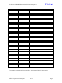
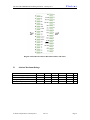
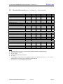
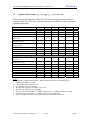
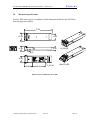
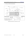
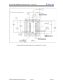
Finisar
Product Specification
RoHS-6 Compliant
10Gb/s DWDM 40km Multi-Rate XFP Optical Transceiver
FTLX3611M3xx
PRODUCT FEATURES
•
Supports 9.95Gb/s to 11.1Gb/s
bit rates
•
Hot-pluggable XFP footprint
•
Maximum link length of 40km
•
Temperature-stabilized DWDMrated EML transmitter
•
RoHS-6 Compliant (lead-free)
•
100GHz ITU Grid, C Band
•
Duplex LC connector
•
DWDM Networks
•
Power dissipation <3.5W
•
•
Built-in digital diagnostic functions
SONET OC-192 IR-2
SDH STM S-64.2b
•
Temperature range: -5°C to 70°C
•
OC-192/STM-64 with FEC
•
10GBASE-ER/EW
•
40km 10G Fibre Channel
•
10GBASE-ER/EW with FEC
APPLICATIONS
Finisar’s 40km FTLX3611M3xx Small Form Factor 10Gb/s (XFP) transceivers comply
with the current XFP Multi-Source Agreement (MSA) Specification1. They comply with
SONET OC-192 IR-2 and SDH STM S-64.2b, as well as with 10-Gigabit Ethernet
10GBASE-ER/EW per IEEE 802.3ae and 10-Gigabit Fibre Channel. Digital diagnostics
functions are available via a 2-wire serial interface, as specified in the XFP MSA. The
transceiver is RoHS compliant and lead free per Directive 2002/95/EC3, and Finisar
Application Note AN-20384.
PRODUCT SELECTION
FTLX3611M3xx
xx: 100GHz ITU Grid wavelength (see next page)
© Finisar Corporation 11-January-2011
Rev C1
Page 1
FTLX3611M3 DWDM XFP Product Specification – January 2011
Channel #
17*
18
19
20
21
22
23
24
25
26
27
28
29
30
31
32
33
34
35
36
37
38
39
40
41
42
43
44
45
46
47
48
49
50
51
52
53
54
55
56
57
58
59
60
61*
Product Code
FTLX3611M317
FTLX3611M318
FTLX3611M319
FTLX3611M320
FTLX3611M321
FTLX3611M322
FTLX3611M323
FTLX3611M324
FTLX3611M325
FTLX3611M326
FTLX3611M327
FTLX3611M328
FTLX3611M329
FTLX3611M330
FTLX3611M331
FTLX3611M332
FTLX3611M333
FTLX3611M334
FTLX3611M335
FTLX3611M336
FTLX3611M337
FTLX3611M338
FTLX3611M339
FTLX3611M340
FTLX3611M341
FTLX3611M342
FTLX3611M343
FTLX3611M344
FTLX3611M345
FTLX3611M346
FTLX3611M347
FTLX3611M348
FTLX3611M349
FTLX3611M350
FTLX3611M351
FTLX3611M352
FTLX3611M353
FTLX3611M354
FTLX3611M355
FTLX3611M356
FTLX3611M357
FTLX3611M358
FTLX3611M359
FTLX3611M360
FTLX3611M361
Frequency (THz)
191.7
191.8
191.9
192.0
192.1
192.2
192.3
192.4
192.5
192.6
192.7
192.8
192.9
193.0
193.1
193.2
193.3
193.4
193.5
193.6
193.7
193.8
193.9
194.0
194.1
194.2
194.3
194.4
194.5
194.6
194.7
194.8
194.9
195.0
195.1
195.2
195.3
195.4
195.5
195.6
195.7
195.8
195.9
196.0
196.1
Finisar
Center Wavelength (nm)
1563.86
1563.05
1562.23
1561.42
1560.61
1559.79
1558.98
1558.17
1557.36
1556.55
1555.75
1554.94
1554.13
1553.33
1552.52
1551.72
1550.92
1550.12
1549.32
1548.51
1547.72
1546.92
1546.12
1545.32
1544.53
1543.73
1542.94
1542.14
1541.35
1540.56
1539.77
1538.98
1538.19
1537.40
1536.61
1535.82
1535.04
1534.25
1533.47
1532.68
1531.90
1531.12
1530.33
1529.55
1528.77
*This channel is supported with limited availability -- Please contact Finisar for further details.
© Finisar Corporation 11-January-2011
Rev C1
Page 2
FTLX3611M3 DWDM XFP Product Specification – January 2011
Finisar
I. Pin Descriptions
Pin
1
2
3
Logic
LVTTL-I
4
LVTTL-O
5
6
7
8
9
10
11
LVTTL-I
Symbol
GND
VEE5
Mod-Desel
Interrupt
TX_DIS
VCC5
GND
VCC3
VCC3
SCL
SDA
12
LVTTL-I
LVTTLI/O
LVTTL-O
Mod_Abs
13
LVTTL-O
Mod_NR
14
15
16
17
18
19
20
21
LVTTL-O
LVTTL-I
RX_LOS
GND
GND
RDRD+
GND
VCC2
P_Down/RST
22
23
24
PECL-I
VCC2
GND
RefCLK+
25
PECL-I
RefCLK-
26
27
28
29
30
CML-O
CML-O
CML-I
CML-I
GND
GND
TDTD+
GND
Name/Description
Module Ground
Optional –5.2 Power Supply – Not required
Module De-select; When held low allows the module to
respond to 2-wire serial interface commands
Interrupt (bar); Indicates presence of an important condition
which can be read over the serial 2-wire interface
Transmitter Disable; Transmitter laser source turned off
+5 Power Supply
Module Ground
+3.3V Power Supply
+3.3V Power Supply
Serial 2-wire interface clock
Serial 2-wire interface data line
Ref.
1
Module Absent; Indicates module is not present. Grounded
in the module.
Module Not Ready; Finisar defines it as a logical OR
between RX_LOS and Loss of Lock in TX/RX.
Receiver Loss of Signal indicator
Module Ground
Module Ground
Receiver inverted data output
Receiver non-inverted data output
Module Ground
+1.8V Power Supply
Power Down; When high, places the module in the low
power stand-by mode and on the falling edge of P_Down
initiates a module reset
Reset; The falling edge initiates a complete reset of the
module including the 2-wire serial interface, equivalent to a
power cycle.
+1.8V Power Supply
Module Ground
Reference Clock non-inverted input, AC coupled on the
host board – Not required
Reference Clock inverted input, AC coupled on the host
board – Not required
Module Ground
Module Ground
Transmitter inverted data input
Transmitter non-inverted data input
Module Ground
2
2
1
2
2
2
2
1
1
1
1
1
1
1
Notes:
1. Module circuit ground is isolated from module chassis ground within the module.
2. Open collector; should be pulled up with 4.7k – 10kohms on host board to a voltage between 3.15V
and 3.6V.
© Finisar Corporation 11-January-2011
Rev C1
Page 3
Finisar
FTLX3611M3 DWDM XFP Product Specification – January 2011
Diagram of Host Board Connector Block Pin Numbers and Names
II.
Absolute Maximum Ratings
Parameter
Maximum Supply Voltage 1
Maximum Supply Voltage 2
Storage Temperature
Case Operating Temperature
© Finisar Corporation 11-January-2011
Symbol
Vcc3
Vcc5
TS
TOP
Min
-0.5
-0.5
-40
-5
Rev C1
Typ
Max
4.0
6.0
85
70
Unit
V
V
°C
°C
Ref.
Page 4
Finisar
FTLX3611M3 DWDM XFP Product Specification – January 2011
III.
Electrical Characteristics (TOP = -5 to 70 °C, VCC5 = 4.75 to 5.25 Volts)
Parameter
Main Supply Voltage
Supply Voltage #2
Supply Voltage #3
Supply Current – Vcc5 supply
Supply Current – Vcc3 supply
Supply Current – Vcc2 supply
Module total power
Transmitter
Input differential impedance
Differential data input swing
Transmit Disable Voltage
Transmit Enable Voltage
Transmit Disable Assert Time
Receiver
Differential data output swing
Data output rise time
Data output fall time
LOS Fault
LOS Normal
Power Supply Rejection
Reference Clock
Clock differential input impedance
Reference Clock frequency
Differential clock input swing
Clock output rise/fall time
Reference clock frequency tolerance
Symbol
Vcc5
Vcc3
Vcc2
Icc5
Icc3
Icc2
P
Rin
Vin,pp
VD
VEN
Vout,pp
tr
tf
VLOS fault
VLOS norm
PSR
Rclkin
f0
Vclkin,pp
trf
Df
Min
4.75
3.13
1.71
Typ
Max
5.25
3.45
1.89
350
400
750
3.5
Unit
V
V
V
mA
mA
mA
W
Ω
mV
V
V
us
2
820
Vcc
GND+ 0.8
10
650
mV
ps
ps
V
V
4
5
5
6
6
7
100
Baud/64
Ω
MHz
mV
ps
PPM
100
120
2.0
GND
340
Vcc – 0.5
GND
640
200
-100
850
38
38
VccHOST
GND+0.5
See Note 6 below
1600
1250
+100
Ref.
1
3
5
Notes:
1. Maximum total power value is specified across the full temperature and voltage range.
2. After internal AC coupling.
3. Or open circuit.
4. Into 100 ohms differential termination.
5. 20 – 80 %
6. Loss Of Signal is open collector to be pulled up with a 4.7k – 10kohm resistor to 3.15 – 3.6V. Logic 0
indicates normal operation; logic 1 indicates no signal detected.
7. Per Section 2.7.1. in the XFP MSA Specification1.
© Finisar Corporation 11-January-2011
Rev C1
Page 5
Finisar
FTLX3611M3 DWDM XFP Product Specification – January 2011
IV.
Optical Characteristics (TOP = -5 to 70°C, VCC5 = 4.75 to 5.25 Volts)
Please note that the Transmitter of the FTLX3611M3 becomes operational within 60
seconds of power-up. This is due to the time required for the EML to reach its optimum
operating temperature.
Parameter
Transmitter
Output Opt. Pwr: 9/125 SMF
Optical Extinction Ratio
Center Wavelength Spacing
Transmitter Center Wavelength –
End Of Life
Transmitter Center Wavelength –
Beginning Of Life
Transmitter Dispersion Penalty
(@ 800 ps/nm)
Sidemode Supression ratio
Tx Jitter Generation (peak-to-peak)
Tx Jitter Generation (RMS)
Symbol
Min
Max
Unit
Ref.
POUT
ER
-1
8.2
+2
X+100
dBm
dB
GHz
pm
1
1
2
3
λc
X-100
100
X
λc
X-25
X
X+25
pm
3
2
dB
0.1
0.01
dB
UI
UI
Relative Intensity Noise
Receiver
Receiver Sensitivity @ 9.95Gb/s to
11.1Gb/s
Stressed Receiver Sensitivity
(OMA) @ 11.1Gb/s
Maximum Input Power
Optical Center Wavelength
Receiver Reflectance
Path penalty at 40km
LOS De-Assert
LOS Assert
LOS Hysteresis
RIN
-130
dB/Hz
RSENS1
-16
dBm
6
RSENS2
-11.3
dBm
7
dBm
nm
dB
dB
dBm
dBm
dB
8
TDP
SSRmin
Txj
TxjRMS
PMAX
λC
Rrx
LOSD
LOSA
Typ
30
-1
1270
-28
0.5
1600
-27
2
-22
4
5
Notes:
1. Having ER=8.2dB guarantees that the –1 dBm minimum output power meets IEEE 802.3ae
requirement of OMA = -2.4 dBm.
2. Corresponds to approximately 0.8 nm.
3. X = Specified ITU Grid wavelength.
4. Measured with a host jitter of 50 mUI peak-to-peak.
5. Measured with a host jitter of 7 mUI RMS.
6. Measured with worst ER; BER<10-12; PRBS31. Equivalent to –14.3 dBm OMA at ER = 8.2 dB.
7. Per IEEE 802.3ae. Equivalent to –14.3 dBm average power at Infinite ER.
8. Dispersion penalty is measured in loopback using 18 ps/(nm*km) fiber (SMF-28).
© Finisar Corporation 11-January-2011
Rev C1
Page 6
Finisar
FTLX3611M3 DWDM XFP Product Specification – January 2011
V.
General Specifications
Parameter
Bit Rate
Bit Error Ratio
Max. Supported Link Length
Symbol
BR
BER
LMAX
Min
9.95
Typ
Max
11.1
10-12
40
Units
Gb/s
km
Ref.
1
2
1
Notes:
1. SONET OC-192 IR-2, 10GBASE-ER/EW, SONET OC-192 with FEC, 10GBASE-ER/EW with FEC
2. Tested with a 231 – 1 PRBS
VI.
Environmental Specifications
Finisar XFP transceivers have an operating temperature range from -5°C to +70°C case
temperature.
Parameter
Case Operating Temperature
Storage Temperature
VII.
Symbol
Top
Tsto
Min
-5
-40
Typ
Max
70
85
Units
°C
°C
Ref.
Regulatory Compliance
Finisar XFP transceivers are Class 1 Laser Products. They are certified per the following
standards:
Feature
Agency
Standard
Laser Eye
Safety
Laser Eye
Safety
FDA/CDRH
CDRH 21 CFR 1040 and Laser Notice 50
TÜV
72101686
Electrical
Safety
Electrical
Safety
TÜV
EN 60825-1: 2007, EN60825-2:2004+A1
IEC 60825-1: 2007 (2nd Edition)
IEC 60825-2: 2010 (3rd Edition)
EN 60950:2006+A11
CLASS 3862.07
CLASS 3862.87
2283290
UL/CSA
Certificate
Number
9210176-77
72101686
Copies of the referenced certificates are available at Finisar Corporation upon request.
© Finisar Corporation 11-January-2011
Rev C1
Page 7
FTLX3611M3 DWDM XFP Product Specification – January 2011
Finisar
VIII. Digital Diagnostics Functions
As defined by the XFP MSA1, Finisar XFP transceivers provide digital diagnostic
functions via a 2-wire serial interface, which allows real-time access to the following
operating parameters:
•
•
•
•
•
Transceiver temperature
Laser bias current
Transmitted optical power
Received optical power
Transceiver supply voltage
It also provides a sophisticated system of alarm and warning flags, which may be used to
alert end-users when particular operating parameters are outside of a factory-set normal
range.
The operating and diagnostics information is monitored and reported by a Digital
Diagnostics Transceiver Controller (DDTC) inside the transceiver, which is accessed
through the 2-wire serial interface. When the serial protocol is activated, the serial clock
signal (SCL pin) is generated by the host. The positive edge clocks data into the XFP
transceiver into those segments of its memory map that are not write-protected. The
negative edge clocks data from the XFP transceiver. The serial data signal (SDA pin) is
bi-directional for serial data transfer. The host uses SDA in conjunction with SCL to
mark the start and end of serial protocol activation. The memories are organized as a
series of 8-bit data words that can be addressed individually or sequentially. The 2-wire
serial interface provides sequential or random access to the 8 bit parameters, addressed
from 000h to the maximum address of the memory.
For more detailed information, including memory map definitions, please see the XFP
MSA documentation1.
© Finisar Corporation 11-January-2011
Rev C1
Page 8
Finisar
FTLX3611M3 DWDM XFP Product Specification – January 2011
IX.
Mechanical Specifications
Finisar’s XFP transceivers are compliant with the dimensions defined by the XFP MultiSourcing Agreement (MSA).
77.95
22.15
18.35
13.30
8.50
LATCHED
1.95
16.00
UNLATCHED
20.85
R1.00
39.00
XFP Transceiver (dimensions are in mm)
© Finisar Corporation 11-January-2011
Rev C1
Page 9
FTLX3611M3 DWDM XFP Product Specification – January 2011
X.
Finisar
PCB Layout and Bezel Recommendations
XFP Host Board Mechanical Layout (dimensions are in mm)
© Finisar Corporation 11-January-2011
Rev C1
Page 10
FTLX3611M3 DWDM XFP Product Specification – January 2011
Finisar
XFP Detail Host Board Mechanical Layout (dimensions are in mm)
© Finisar Corporation 11-January-2011
Rev C1
Page 11
FTLX3611M3 DWDM XFP Product Specification – January 2011
Finisar
XFP Recommended Bezel Design (dimensions are in mm)
© Finisar Corporation 11-January-2011
Rev C1
Page 12
FTLX3611M3 DWDM XFP Product Specification – January 2011
Finisar
XI.
References
1.
10 Gigabit Small Form Factor Pluggable Module (XFP) Multi-Source Agreement
(MSA), Rev 4.5 – August 2005. Documentation is currently available at
http://www.xfpmsa.org/
2.
Application Note AN-2035: “Digital Diagnostic Monitoring Interface for XFP
Optical Transceivers” – Finisar Corporation, December 2003
3.
Directive 2002/95/EC of the European Council Parliament and of the Council,
“on the restriction of the use of certain hazardous substances in electrical and
electronic equipment”. January 27, 2003.
4.
“Application Note AN-2038: Finisar Implementation Of RoHS Compliant
Transceivers”, Finisar Corporation, January 21, 2005.
XII.
Revision History
Revision
Date
A
4/12/2006
A1
XII.
4/21/2006
Description
•
Document created.
•
Added OC-192/STM-64 with FEC in applications section
•
Removed Finisar Confidential from footer.
•
Replaced product photo.
•
Updated BOL wavelength tolerance specification.
•
Updated Finisar Address.
•
Added Safety Certificate numbers.
•
Document release.
A2
5/22/2006
B
10/25/2006
B1
9/28/2007
•
Updated note on channel.
B2
2/7/2008
•
Added channel column.
C1
1/11/2011
•
Update Channel Availability
For More Information
Finisar Corporation
1389 Moffett Park Drive
Sunnyvale, CA 94089-1133
Tel. 1-408-548-1000
Fax 1-408-541-6138
[email protected]
www.finisar.com
© Finisar Corporation 11-January-2011
Rev C1
Page 13