Transcript
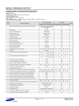
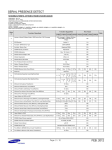
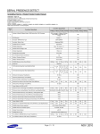
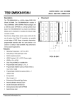
HMT41GV7BMR4C-G7/H9
SERIAL PRESENCE DETECT
G7 D2
Function described
0
1
2
3
4
5
6
7
8
9
10
11
12
13
14
15
16
17
18
19
20
21
22
23
24
25
26
27
28
29
30
31
32
33
34~59
60
61
62
63
64
65
66
67
68
69
70
71
72
73
74
75~116
117
118
119
120
121
122~125
126
127
128
129
130
131
132
133
134
135
136
137
138
139
140
141
142
143
144
145
146
147
148
149
150~175
176~255
CRC Coverage/SPD Device Size/Number of Serial PD Bytes written
SPD Revision
DRAM Device Type
Module Type
SDRAM Density and Banks
SDRAM Addressing(Row/Column)
Module Nominal Voltage, VDD
Module Organization (rank / data bit width)
Module Memory Bus Width
Fine Timebase Dividened and Divisor
Medium Timebase Dividened
Medium Timebase Divisor
Minimum SDRAM Cycle Time(tCKmin)
Reserved
SDRAM CAS Latency Supported, Low Byte
~~~~SDRAM CAS Latency Supported, High Byte
Minimum CAS Latency Time(tAAmin)
Minimum Write Recovery Time(tWRmin)
Minimum /RAS to /CAS Delay (tRCDmin)
Minimun Row Active to Row Active Delay (tRRDmin)
Minimum Row Precharge Delay Time (tRPmin)
Upper Nibbles for tRAS and tRC
Minimum Active to Precharge Delay Time (tRASmin), Least Significant Byte
~~~~Minimum Active to Active/Refresh Delay Time (tRCmin), Least Significant Byte
Minimum Refresh Recovery Time(tRFCmin), Least Significant Byte
~~Minimum Refresh Recovery Time(tRFCmin), Least Significant Byte
Minimum Internal Write to Read Command Delay Time(tWTRmin)
Minimum Internal Read to Precharge Command Delay Time(tRTPmin)
Upper Nibble for tFAW
~~~~Minimum Four Active Window Delay Time(tFAW), Least Significant Byte
SDRAM Output DriverSupported
SDRAM Thermal and Refresh Options
Module Thermal Sensor
SDRAM Device Type
Reserved
Module Nominal Height of Unbuffered Dimm
Module Maximum Thickness of unbuffered DIMM
Reference Raw Card Used for unbuffered DIMM
DIMM Module Attributes
Heat Spreader Solution
Register Vendor ID (LSB)
Register Vendor ID (MSB)
Register Revision Number
Register Type
Register Control Word Function RC1 / RC0
Register Control Word Function RC 3 / RC 2
Register Control Word Function RC 5 / RC 4
Reserved
Reserved
Register Control Word Function RC11 / RC10
Reserved
Module Manufacturer JEDEC ID Code, Least Significant Byte
~~~~Module Manufacturer JEDEC ID Code, Most Significant Byte
Module Manufacturing location
Module Manufacturing Data (Year)
Module Manufacturing Data (Week)
Module Serial Number
Cyclical Redundancy Code
~~~~Cyclical Redundancy Code
Manufacture part number ( Hynix Memory Module )
~~~~Manufacture part number ( Hynix Memory Module )
Component Group (DDR3 SDRAM)
Component Density
Manufacture part number ( Memory Depth )
~~~~Manufacture part number ( Memory Depth)
Manufacture part number ( Module type )
Manufacture part number ( Data width )
Manufacture part number ( Die generation)
Manufacture part number ( Package Type)
Manufacture part number ( Package Material)
Manufacture part number ( Component configuration)
Manufacture part number ( Power consumption & Temp.)
Manufacture part number ( Hyphen )
Manufacture part number ( Speed)
~~~~Manufacture part number ( Speed)
Manufacture part number
Manufacture part number
Module Revision Code
~~~Module Revision Code
DRAM Manufacturer JEDEC ID Code, Least Significant Byte
Function support
116/256/176 Bytes
1.0
DDR3 SDRAM
Registered DIMM
8 banks, 2Gb
15 / 11
Only 1.5V Operable
2rank/x4
ECC/ 72bit bus
5ps / 2
1ns
8
1.875ns
Blank
6,7,8
Not support over CL=12
13.125 ns
15ns
13.125 ns
7.5ns
13.125 ns
Refer to Byte22,23
37.5 ns
50.625 ns
160ns
160ns
7.5ns
7.5ns
Refer to Byte29
37.5 ns
DLL Off, RZQ/6, RZQ/7
ASR, Normal Temp
TS incorporated
DDP
Blank
19.4mm
3~4mm
rev 0.0 / RC N
1Row 1Register
Present
Inphi
Inphi
GS-02 LV
SSTE32882
rev 0.0 / RC N
rev 0.0 / RC N
rev 0.0 / RC N
Blank
Blank
Inphi 1.5V for RC11
Blank
Hynix
Hynix
Hynix(Ichon)
Variable
Variable
Undefined
CRC cover 0~116 byte
CRC cover 0~116 byte
H
M
T
4
1
G
V
7
B
M
R
4
C
G
7
Blank
Blank
D
2
Hynix
~~~~DRAM Manufacturer JEDEC ID Code, Most Significant Byte
Manufacturer's Specific Data
Open for customer use
Blank
Blank
G7 D7
HEX
92
10
0B
01
03
1A
00
08
0B
52
01
08
0F
00
1C
00
69
78
69
3C
69
11
2C
95
00
05
3C
3C
01
2C
83
05
80
80
00
05
33
0C
05
80
04
B3
11
00
00
A0
55
00
00
00
00
80
AD
01
00
00
00
9A
AC
48
4D
54
34
31
47
56
37
42
4D
52
34
43
2D
47
37
20
20
44
32
80
AD
00
00
Function support
116/256/176 Bytes
1.0
DDR3 SDRAM
Registered DIMM
8 banks, 2Gb
15 / 11
Only 1.5V Operable
2rank/x4
ECC/ 72bit bus
5ps / 2
1ns
8
1.875ns
Blank
6,7,8
Not support over CL=12
13.125 ns
15ns
13.125 ns
7.5ns
13.125 ns
Refer to Byte22,23
37.5 ns
50.625 ns
160ns
160ns
7.5ns
7.5ns
Refer to Byte29
37.5 ns
DLL Off, RZQ/6, RZQ/7
ASR, Normal Temp
TS incorporated
DDP
Blank
19.4mm
3~4mm
rev 0.0 / RC N
1Row 1Register
Present
IDT
IDT
B
SSTE32882
rev 0.0 / RC N
rev 0.0 / RC N
rev 0.0 / RC N
Blank
Blank
IDT 1.5V for RC11
Blank
Hynix
Hynix
Hynix(Ichon)
Variable
Variable
Undefined
CRC cover 0~116 byte
CRC cover 0~116 byte
H
M
T
4
1
G
V
7
B
M
R
4
C
G
7
Blank
Blank
D
7
Hynix
Blank
Blank
H9 D2
HEX
92
10
0B
01
03
1A
00
08
0B
52
01
08
0F
00
1C
00
69
78
69
3C
69
11
2C
95
00
05
3C
3C
01
2C
83
05
80
80
00
05
33
0C
05
80
80
B3
61
00
00
A0
55
00
00
00
00
80
AD
01
00
00
00
82
92
48
4D
54
34
31
47
56
37
42
4D
52
34
43
2D
47
37
20
20
44
37
80
AD
00
00
Function support
116/256/176 Bytes
1.0
DDR3 SDRAM
Registered DIMM
8 banks, 2Gb
15 / 11
Only 1.5V Operable
2rank/x4
ECC/ 72bit bus
5ps / 2
1ns
8
1.5ns
Blank
6,7,8,9
Not support over CL=12
13.125ns
15ns
13.125ns
6ns
13.125ns
Refer to Byte22,23
36ns
49.125 ns
160ns
160ns
7.5ns
7.5ns
Refer to Byte29
30 ns
DLL Off, RZQ/6, RZQ/7
ASR, Normal Temp
TS incorporated
DDP
Blank
19.4mm
3~4mm
rev 0.0 / RC N
1Row 1Register
Present
Inphi
Inphi
GS-02 LV
SSTE32882
rev 0.0 / RC N
rev 0.0 / RC N
rev 0.0 / RC N
Blank
Blank
Inphi 1.5V for RC11
Blank
Hynix
Hynix
Hynix(Ichon)
Variable
Variable
Undefined
CRC cover 0~116 byte
CRC cover 0~116 byte
H
M
T
4
1
G
V
7
B
M
R
4
C
H
9
Blank
Blank
D
2
Hynix
Blank
Blank
H9 D7
HEX
92
10
0B
01
03
1A
00
08
0B
52
01
08
0C
00
3C
00
69
78
69
30
69
11
20
89
00
05
3C
3C
00
F0
83
05
80
80
00
05
33
0C
05
80
04
B3
11
00
00
A0
55
00
00
00
00
80
AD
01
00
00
00
D8
05
48
4D
54
34
31
47
56
37
42
4D
52
34
43
2D
48
39
20
20
44
32
80
AD
00
00
Function support
116/256/176 Bytes
1.0
DDR3 SDRAM
Registered DIMM
8 banks, 2Gb
15 / 11
Only 1.5V Operable
2rank/x4
ECC/ 72bit bus
5ps / 2
1ns
8
1.5ns
Blank
6,7,8,9
Not support over CL=12
13.125ns
15ns
13.125ns
6ns
13.125ns
Refer to Byte22,23
36ns
49.125 ns
160ns
160ns
7.5ns
7.5ns
Refer to Byte29
30 ns
DLL Off, RZQ/6, RZQ/7
ASR, Normal Temp
TS incorporated
DDP
Blank
19.4mm
3~4mm
rev 0.0 / RC N
1Row 1Register
Present
IDT
IDT
B
SSTE32882
rev 0.0 / RC N
rev 0.0 / RC N
rev 0.0 / RC N
Blank
Blank
IDT 1.5V for RC11
Blank
Hynix
Hynix
Hynix(Ichon)
Variable
Variable
Undefined
CRC cover 0~116 byte
CRC cover 0~116 byte
H
M
T
4
1
G
V
7
B
M
R
4
C
H
9
Blank
Blank
D
7
Hynix
Blank
Blank
HEX
92
10
0B
01
03
1A
00
08
0B
52
01
08
0C
00
3C
00
69
78
69
30
69
11
20
89
00
05
3C
3C
00
F0
83
05
80
80
00
05
33
0C
05
80
80
B3
61
00
00
A0
55
00
00
00
00
80
AD
01
00
00
00
C0
3B
48
4D
54
34
31
47
56
37
42
4D
52
34
43
2D
48
39
20
20
44
37
80
AD
00
00