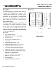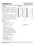
1
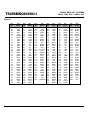
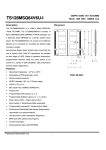
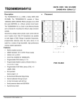
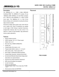
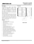
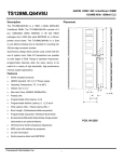
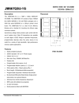
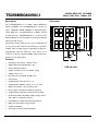
200PIN DDR2 667 SO-DIMM
TS256MSQ64V6U-I
2Rank 2GB With 128Mx8 CL5
Description
Placement
The TS256MSQ64V6U-I is a 256M x 64bits DDR2-667
2Rank SO-DIMM. The TS256MSQ64V6U-I consists of
16pcs 128Mx8bits DDR2 SDRAMs in FBGA packages
and a 2048 bits serial EEPROM on a 200-pin printed
D
circuit board. The TS256MSQ64V6U-I is a Dual In-Line
B A
Memory Module and is intended for mounting into 200-pin
edge connector sockets.
Synchronous design allows precise cycle control with the
E
use of system clock. Data I/O transactions are possible
C
on both edges of DQS. Range of operation frequencies,
G
programmable latencies allow the same device to be
useful for a variety of high bandwidth, high performance
H
memory system applications.
I
Features
•
Operating Temperature : -40°C to +85°C
•
Gold plating of PCB gold finger is 30u
•
RoHS compliant products.
•
JEDEC standard 1.8V ± 0.1V Power supply
•
VDDQ=1.8V ± 0.1V
•
Max clock Freq: 333MHZ; 667Mb/s/Pin.
•
Posted CAS
•
Programmable CAS Latency: 3, 4, 5
•
Programmable Additive Latency :0, 1, 2, 3 and 4
•
Write Latency (WL) = Read Latency (RL)-1
•
Burst Length: 4,8(Interleave/nibble sequential)
•
Programmable sequential / Interleave Burst Mode
•
Bi-directional Differential Data-Strobe (Single-ended
J
PCB: 09-2166
data-strobe is an optional feature)
•
Off-Chip Driver (OCD) Impedance Adjustment
•
MRS cycle with address key programs.
•
On Die Termination
•
Serial presence detect with EEPROM
Transcend Information Inc.
1
F
K
200PIN DDR2 667 SO-DIMM
TS256MSQ64V6U-I
2Rank 2GB With 128Mx8 CL5
Dimensions
Side
Pin Identification
Millimeters
Inches
Symbol
Function
A
67.6±0.15
2.661±0.006
A0~A13, BA0~BA2
Address input
B
63.6
2.503
DQ0~DQ63
Data Input / Output.
C
11.4
0.449000
DQS0~DQS7
Data strobe
D
47.4
1.866
/DQS0~/DQS7
Differential Data strobe
E
4.2
0.1650
F
2.15±0.15
0.085±0.006
G
6
0.236
H
18
0.709
I
4
J
K
CK0, /CK0
Clock Input.
CK1, /CK1
CKE0, CKE1
Clock Enable Input.
0.157
ODT0, ODT1
On-die termination control line
30
1.181
/CS0, /CS1
Chip Select Input.
1.0±0.075
0.039±0.003
/RAS
Row Address Strobe
/CAS
Column Address Strobe
/WE
Write Enable
DM0~DM7
Data-in Mask
VDD
+1.8 Voltage power supply
(Refer Placement)
+1.8 Voltage Power Supply for
VDDQ
DQS
VREF
Power Supply for Reference
Serial EEPROM Positive Power
VDDSPD
Supply
Transcend Information Inc.
2
SA0~SA2
Address select for EEPROM
SCL
Serial PD Clock
SDA
Serial PD Add/Data input/output
VSS
Ground
NC
No Connection
200PIN DDR2 667 SO-DIMM
TS256MSQ64V6U-I
2Rank 2GB With 128Mx8 CL5
Pinouts:
Pin
Pin
Pin
Pin
No
Name
No
Name
01
VREF
69
NC
03
VSS
71
VSS
05
DQ0
73
DQ26
07
DQ1
75
DQ27
09
VSS
77
VSS
11
/DQS0
79
CKE0
13
DQS0
81
VDD
15
VSS
83
*/CS2
17
DQ2
85
*BA2
19
DQ3
87
VDD
21
VSS
89
A12
23
DQ8
91
A9
25
DQ9
93
A8
27
VSS
95
VDD
29
/DQS1
97
A5
31
DQS1
99
A3
33
VSS
101
A1
35
DQ10
103
VDD
37
DQ11
105
A10/AP
39
VSS
107
BA0
41
VSS
109
/WE
43
DQ16
111
VDD
45
DQ17
113
/CAS
47
VSS
115
*/CS1
49
/DQS2
117
VDD
51
DQS2
119
*ODT1
53
VSS
121
VSS
55
DQ18
123
DQ32
57
DQ19
125
DQ33
59
VSS
127
VSS
61
DQ24
129
/DQS4
63
DQ25
131
DQS4
65
VSS
133
VSS
67
DM3
135
DQ34
* Please refer Block Diagram
Transcend Information Inc.
Pin
No
137
139
141
143
145
147
149
151
153
155
157
159
161
163
165
167
169
171
173
175
177
179
181
183
185
187
189
191
193
195
197
199
Pin
Pin
Name
No
DQ35
02
VSS
04
DQ40
06
DQ41
08
VSS
10
DM5
12
VSS
14
DQ42
16
DQ43
18
VSS
20
DQ48
22
DQ49
24
VSS
26
NC, TEST 28
VSS
30
/DQS6
32
DQS6
34
VSS
36
DQ50
38
DQ51
40
VSS
42
DQ56
44
DQ57
46
VSS
48
DM7
50
VSS
52
DQ58
54
DQ59
56
VSS
58
SDA
60
SCL
62
VDDSPD 64
66
68
3
Pin
Name
VSS
DQ4
DQ5
VSS
DM0
VSS
DQ6
DQ7
VSS
DQ12
DQ13
VSS
DM1
VSS
CK0
/CK0
VSS
DQ14
DQ15
VSS
VSS
DQ20
DQ21
VSS
NC
DM2
VSS
DQ22
DQ23
VSS
DQ28
DQ29
VSS
/DQS3
Pin
No
70
72
74
76
78
80
82
84
86
88
90
92
94
96
98
100
102
104
106
108
110
112
114
116
118
120
122
124
126
128
130
132
134
136
Pin
Name
DQS3
VSS
DQ30
DQ31
VSS
*CKE1
VDD
*A15
*A14
VDD
A11
A7
A6
VDD
A4
A2
A0
VDD
BA1
/RAS
/CS0
VDD
ODT0
*A13
VDD
*/CS3
VSS
DQ36
DQ37
VSS
DM4
VSS
DQ38
DQ39
Pin
No
138
140
142
144
146
148
150
152
154
156
158
160
162
164
166
168
170
172
174
176
178
180
182
184
186
188
190
192
194
196
198
200
Pin
Name
VSS
DQ44
DQ45
VSS
/DQS5
DQS5
VSS
DQ46
DQ47
VSS
DQ52
DQ53
VSS
CK1
/CK1
VSS
DM6
VSS
DQ54
DQ55
VSS
DQ60
DQ61
VSS
/DQS7
DQS7
VSS
DQ62
DQ63
VSS
SA0
SA1