1
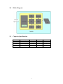
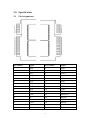
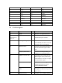
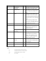
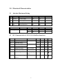
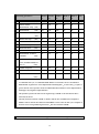
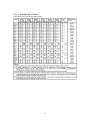
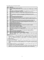
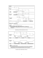
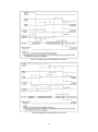
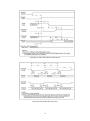
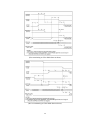
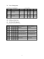
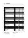
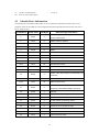
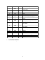
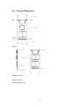
Features: Standard ATA/IDE Bus Interface - 512 Bytes / Sector - ATA comm and set compatible Capacities - Integral Z Series (MLC) 16GB, 32GB, 64GB - Integral E Series (SLC) Please call for availability Data Transfer mode - Support Data Transfer up to PIO mode 6 - Support Data Transfer up to Multiword DMA mode 2 - Support Data Transfer up to Ultra DMA mode 5 Performance Integral Z Series (MLC Flash): Sustain Read Speed up to 35MB/s Sustain Write Speed up to 15MB/s Integral E Series (SLC Flash): Please call for availability Sustain Read Speed up to 45MB/s Sustain Write Speed up to 35MB/s Temperature Ranges - 00C to 700C for operating - -250C to 850C for storage Operating Voltage - 3.3V Intelligent ATA/IDE Module - Built-in Embedded Flash File System - Implements dynamic wear-leveling algorithms and static wear-leveling algorithms to increase endurance of flash media Built-in ECC corrects up to 12 random bits error per 512 bytes RoHS Compliance 2 TABLE OF CONTENTS 1.0 BLOCK DIAGRAM ........................................................................................................................... 4 1.1 CAPACITY SPECIFICATION.................................................................................................... 4 2.0 SPECIFICATION ........................................................................................................................ 5 2.1 PIN ASSIGNMENTS................................................................................................................. 5 2.2 PIN DESCRIPTION ................................................................................................................. 6 3.0 ELECTRICAL CHARACTERISTICS...................................................................................... 8 3.1 ABSOLUTE MAXIMUM RATING ............................................................................................ 8 3.2 DC CHARACTERISTICS OF 5.0V I/O CELLS(HOST INTERFACE) ......................................... 8 3.3 AC CHARACTERISTICS ......................................................................................................... 9 3.3.1 PIO Data Transfer .................................................................................................. 9 3.3.2 Multiword DMA Data Transfer .......................................................................... 12 3.3.3 Ultra DMA Data Transfer .................................................................................... 15 3.4 POWER MANAGEMENT ....................................................................................................... 21 4.0 SOFTWARE INTERFACE ....................................................................................................... 21 4.1 ATA TASK FILE REGISTERS ............................................................................................... 21 4.2 COMMAND SETS.................................................................................................................. 22 4.3 IDENTIFY DRIVE INFORMATION ......................................................................................... 23 5.0 PHYSICAL DIMENSION ........................................................................................................ 25 6.0 WEIGHT .................................................................................................................................... 26 3 1.0 Block Diagram 1.1 Capacity Specification Density Total Bytes Cylinders Heads Sectors 16GB 16,441,270,272 16383 16 63 32GB 32,279,224,320 16383 16 63 64GB 64,558,448,640 16383 16 63 4 2.0 Specification 2.1 Pin Assignments Pin Number Signal Pin Number Signal 1 HD0 2 HD15 3 HD1 4 GND 5 HD2 6 HD14 7 HD3 8 HD13 9 GND 10 HD12 11 HD4 12 HD11 13 HD5 14 HD10 15 GND 16 HD9 17 HD6 18 GND 19 HD7 20 HD8 21 GND 22 nHRESET 23 NC 24 nHIOW 25 NC 26 CSEL 27 GND 28 nHIOR 29 GND 30 nDMACK 31 NC 32 DMARQ 5 33 NC 34 GND 35 GND 36 NC 37 HA0 38 NC 39 HA1 40 GND 41 HA2 42 IORDY 43 nIOIS16 44 INTRQ 45 nPDIAG 46 nHCS0 47 3V3 48 nHCS1 49 3V3 50 GND 51 3V3 52 nDASP 2.2 Pin Description Pin No. Signal I/O* Description 22 -RESET I Hardware reset signal from the host 1, 3, 5, 7, 11, 13, 17, HD0~HD15(Device Data) I/O 16-bit bi-direction Data Bus. DD(7:0) are 19, 20, 16, 14, 12, used for 8-bit register transfers. 10, 8, 6, 2 32 DMARQ(DMA Request) O For DMA data transfers. Device will assert DMARQ when the device is ready to transfer data to or from the host. 24 -DIOW(I/O Write) I This is the strobe signal used by the host to write to the device register or Data port STOP(Stop UDMA Burst) The host assert this signal during an UDMA burst to stop the DMA burst 42 IORDY(I/O channel ready) O This signal is used to temporarily stop the host register access (read or write) when the device is not ready to respond to a data transfer request. DDMARDY(UDMA ready) The device will assert this signal to indicate that the device is ready to receive UDMA data-out burst. DSTROBE(UDMA data When UDMA mode DMA Read is active, strobe) this signal is the data-in strobe generated by the device. 26 CSEL(Cable select) I 6 This pin is used to configure this device as Device 0 or Device 1. 30 -DMACK(DMA I acknowledge) 44 This signal is used by the host in respond to DMARQ to initiate DMA transfer. INTRQ(Interrupt) O When this device is selected, this signal is the active high Interrupt Request to the host 43 IOIS16 O During PIO transfer mode0,1or 2, this pin indicates to the host the 16-bit data port has been addressed and the device is prepared to send or receive a 16-bit data word. When transferring in DMA mode, the host must use a 16-bit DMA channel and this signal will not be asserted. 37, 39, 41 HA0~HA2(Device Address) I This is 3-bit binary coded Address Bus. 45 -PDIAG(Passed diagnostics) I/O This signal will be asserted by Device 1 to indicate to Device 0 that Device 1 has completed diagnostics, -CBLID(Cable assembly type identify) 46,48 -CS0, -CS1(Chip select) I These signals are used to select the Command Block and Control Block registers. When –DMACK is asserted, -Cs0 and –Cs1 shall be negated and transfers shall be 16-bit wide. 52 -DASP(Device active, Device I/O 1 present) During the reset protocol, -DASP shall be asserted by Device 1 to indicate that the device is present. 47, 49, 51 VCC P Power supply 9, 15, 21, 27, 29, 35, GND -- Ground. 4, 18, 26, 34, 40, 50 *Note: “I” An input from the host system to the device. “O” An output from the device to the host system. “I/O” An input/output(bi-direction) common. “P” Power supply. 7 3.0 Electrical Characteristics 3.1 Absolute Maximum Rating Item Symbol Parameter MIN MAX Unit 1 VDD-VSS DC Power Supply -0.3 +5.5 V 2 VIN Input Voltage Vss-0.3 VDD+0.3 V 3 Ta Operating Temperature 0 +70 0 4 Tst Storage Temperature -25 +85 0 C C Parameter Symbol MIN TYP MAX Unit VDD Voltage VDD 3.0 3.3 3.6 V 4.5 5.0 5.5 V 3.2 DC Characteristics of 5.0V I/O Cells(Host Interface) Symbol Parameter Conditions Vil Input Low Voltage TTL(5V) Vih Input High Voltage Vil Input Low Voltage TYP MAX -- -- 0.85 V 1.25 -- -- V -- -- 1.05 V Vih Input High Voltage 1.75 -- -- V Vol Output Low Voltage |Iol| = 4~32 mA -- -- 0.4 V Voh Output High Voltage |Ioh|= 4~32 mA 2.4 -- -- V Iin Input Leakage Current No pull-up or pull -10 ±1 10 μA -10 ±1 10 μA TTL(3.3V) MIN Unit down Ioz Tri-state Output Leakage Current 8 3.3 AC Characteristics 3.3.1 PIO Data Transfer 9 PIO timing parameters t0 Cycle time t1 Address valid to (min) DIOR-/DIOW- setup (min) t2 DIOR-/DIOW- (min) t2i DIOR-/DIOW- recovery time Mode 0 Mode 1 Mode2 Mode 3 Mode 4 Note ns ns ns ns ns 600 383 240 180 120 70 50 30 30 25 165 125 100 80 70 1 -- -- -- 70 25 1 1,4 (min) t3 DIOW- data setup (min) 60 45 30 30 20 t4 DIOW- data hold (min) 30 20 15 10 10 t5 DIOR- data setup (min) 50 35 20 20 20 t6 DIOR- data hold (min) 5 5 5 5 5 t6z DIOR- data tristate (max) 30 30 30 30 30 2 t9 DIOR-/DIOW- to address 20 15 10 10 10 10 0 0 0 0 0 35 35 35 35 35 1250 1250 1250 1250 1250 5 5 5 5 5 valid hold tRD (min) Read Data Valid to IORDY active (if IORDY initially low after tA) (min) tA IORDY Setup time tB IORDY Pulse Width tC IORDY assertion to release (max) 3 (max) Notes1. t0 is minimum total cycle, t2 is minimum DIOR-/DIOW- assertion time, and t2i is the minimum DIOR-/DIOW- negation time. A host implementation shall lengthen t2i to ensure that t0 is equal to or greater than the value reported in the devices IDENTIFY DEVICE data. A device implementation shall support any length host implementation. 2. This parameter specifies the time from the negation edge of DIOR- to the time that the data is released by the device. 3. The delay from the activation of FIOR- or DIOW- until the state of IORDY is first sampled. If IORDY is inactive then the host shall wait until IORDY is active before the PIO cycle is complete. If the device is not driving IORDY negated at the tA after the activation of DIOR- or DIOW-, that t5 shall be met and tRD is not applicable. If the device is driving IORDY 10 negated at the time tA after the activation of DIOR- or DIOW-, then tRD shall be met and t5 is not applicable. 4. Mode may be selected at the highest mode for the device if CS(1:0) and DA(2:0) do not change between read or write cycle or selects at the highest mode supported by the slowest device if CS(1:0) and DA(2:0) do change between read or write cycles. 11 3.3.2 Multiword DMA Data Transfer (Initialing a Multiword DMA data burst) (Sustaining a Multiword DMA data burst) 12 (Device terminating a Multiword DMA data burst) (Host terminating a Multiword DMA data burst) 13 Multiword DMA timing parameters Mode 0 Mode 1 Mode2 ns ns ns Note t0 Cycle time (min) 480 150 120 See note tD DIOR-/DIOW- asserted pulse width (min) 215 80 70 See note tE DIOR- data access (max) 150 60 50 tF DIOR- data hold (min) 5 5 5 tG DIOR-/DIOW- data setup (min) 100 30 20 tH DIOW- data hold (min) 20 15 10 tI DMACK to DIOR-/DIOW- setup (min) 0 0 0 tJ DIOR-/DIOW- to DMACK hold (min) 20 5 5 tKR DIOR- negated pulse width (min) 50 50 25 See note tKW DIOW- negated pulse width (min) 215 50 25 See note tLR DIOR- to DMACK delay (max) 120 40 35 tLW DIOW- to DMACK delay (max) 40 40 35 tM CS(1:0) valid to DIOR-/DIOW- (min) 50 30 25 tN CS(1:0) hold (min) 15 10 10 tZ DMACK- to read data released (max) 20 25 25 Notes- t0 is the minimum total cycle. tD is the minimum DIOR-/DIOW- assertion time, and tK(tKR or tKW, as appropriate) is the minimum DIOR-/DIOW- negation time. A host shall lengthen tD and/or tK to ensure that t0 is equal to the value reported in the devices IDENTIFY DEVICE data. 14 3.3.3 Ultra DMA Data Transfer Ultra DMA data burst timing requirements 15 Ultra DMA data burst timing descriptions 16 (Initialing an Ultra DMA data-in burst) (Sustained Ultra DMA data-in burst) 17 (Device terminating an Ultra DMA data-in burst) (Host terminating an Ultra DMA data-in burst) 18 (Initialing an Ultra DMA data-out data burst) (Sustained Ultra DMA data-out burst) 19 (Host terminating an Ultra DMA data-out burst) (Device terminating an Ultra DMA data-out burst) 20 3.4 Power Management (Ta = 0 to 700C) System Power Consumption: Symbol Parameter Conditions MIN TYP MAX Unit Iccr Read current 5V - 150 - mA Iccw Write current 5V - 130 - mA Ipd Power down current 5V - 12 Iccr Read current 3.3V - 230 - mA Iccw Write current 3.3V - 200 - mA Ipd Power down current 3.3V - 18 mA mA Note: Test Based on 8 pieces of TSOP flash. 4.0 Software Interface 4.1 ATA Task File Registers The I/O decoding of each register is as follows -CS1 -CS0 A2 A1 A0 -DIOR=0(-DIOW=1) -DIOW=0(-DIOR=1) 1 0 0 0 0 Data(Read) Data(Write) 1 0 0 0 1 Error Feature 1 0 0 1 0 Sector Count Sector Count 1 0 0 1 1 Sector Number (LBA7-0) Sector Number (LBA7-0) 1 0 1 0 0 Cylinder Low (LBA 15-8) Cylinder Low (LBA 15-8) 1 0 1 0 1 Cylinder High (LBA 23-16) Cylinder High(LBA 23-16) 1 0 1 1 0 Drive/Head (LBA 27-24) Drive/Head (LBA 27-24) 1 0 1 1 1 Status Command 0 1 1 1 0 Alternate Status Device Control 0 1 1 1 1 Drive Address Reserved 21 4.2 Command Sets Below table summarizes the PATA PCIe command set with the paragraphs that follow describing the individual commands and task file for each command. No. Command Set Code FR SC SN CY DR HD LBA 1 CFA Erase Sector(s) C0h -- Y Y Y Y Y Y 2 CFA Request Extended Error Code 03h -- -- -- -- Y -- -- 3 CFA Translate Sector 87h -- Y Y Y Y Y Y 4 CFA Write Multiple w/o Erase CDh -- Y Y Y Y Y Y 5 CFA Write Sector w/o Erase 38h -- Y Y Y Y Y Y 6 Check Power Mode E5h -- -- -- -- Y -- -- 7 Execute Device Diagnostic 90h -- -- -- -- Y -- -- 8 Identify Device ECh -- -- -- -- Y -- -- 9 Idle E3h -- Y -- -- Y -- -- 10 Idle Immediate E1h -- -- -- -- Y -- -- 11 Initialize Device Parameters 91h -- Y -- -- Y Y -- 12 NOP 00h -- -- -- -- Y -- -- 13 Read Buffer E4h -- -- -- -- Y -- -- 14 Read DMA C8h -- Y Y Y Y Y Y 15 Read Multiple C4h -- Y Y Y Y Y Y 16 Read Sector(s) 20h -- Y Y Y Y Y Y 17 Read Verify Sector(s) 40h -- Y Y Y Y Y Y 18 Seek 70 -- -- Y Y Y Y Y 19 Set Features EFh Y -- -- -- Y -- -- 20 Set Multiple Mode C6h -- Y -- -- Y -- -- 21 Sleep E6h -- -- -- -- Y -- -- 22 Standby E2h -- -- -- -- Y -- -- 23 Standby Immediate E0h -- -- -- -- Y -- -- 24 Write Buffer E8h -- -- -- -- Y -- -- 25 Write DMA CAh -- Y Y Y Y Y Y 26 Write Multiple C5h -- Y Y Y Y Y Y 27 Write Sector(s) 30h -- Y Y Y Y Y Y Note: FR: Feature Register HD: Head No. of Drive/Head Register SC: Sector Count Register LBA: LBA mode supported SN: Sector Number Register Y: Set up 22 CY: Cylinder Low/High Register DR: Drive bit of Drive/Head register 4.3 --: Not set up Identify Drive Information The Identity Drive Command enables Host to receive parameter information from the device. The parameter words in the buffer have the arrangement and meanings defined in below table. All reserve bits or words are zero. Word Address Default Value Total Bytes Data Field Type Information General configuration – bit significant for 0 044Ah 2 Non-removable device 1 xxxxh 2 Default number of cylinders 2 0000h 2 Reserved 3 xxxxh 2 Default number of heads 4 7E00h 2 Retired 5 0200h 2 Retired 6 xxxxh 2 Default number of sectors per track 7-8 xxxxh 4 Number of sectors per device 9 0000h 2 Retired 10-19 xxxxh 20 Serial Number in ASCII 20 0002h 2 Retired 21 0002h 2 Retired 22 0004h 2 Number of ECC Bytes passed on Read/Write Long Commands 23-26 Aaaah 8 Firmware revision in ASCII 27-46 xxxxh 40 Model number in ASCII 47 8001h 2 Maximum number of sector that shall be transferred on Read/Write Multiple commands 48 0000h 2 Reserved 49 2B00h 2 Capabilities-LBA/DMA Supported 50 4000h 2 Reserved 51 0200h 2 PIO data transfer cycle timing mode 2 52 0000h 2 Retired 53 0007h 2 Word 54-58, 64-70 and 88 are valid 54 xxxxh 2 Current numbers of cylinders 55 xxxxh 2 Current numbers of heads 56 xxxxh 2 Current sectors per track 23 Word Address Default Value Total Bytes Data Field Type Information Current capacity in sectors (LBAs)(Word 57= LSW, 57-58 Nnnnh 4 Word 58= MSW) 59 0101h 2 Multiple sector setting is valid 60-61 Aaaah 4 Total number of sectors addressable in LBA Mode 62 0000h 2 Retired 63 0n07h 2 Multiword DMA mode 2 and below are supported 64 0003h 2 Advance PIO transfer modes supported 65 0078h 2 Minimum Multiword DMA transfer cycle time 120nsec Manufacturer’s recommended Multiword DMA 66 0078h 2 transfer cycle time 120nsec Minimum PIO transfer cycle time without flow 67 0078h 2 control 120nsec Minimum PIO transfer cycle time with IORDY flow 68 0078h 2 control 120nsec 69-81 0000h 26 Reserved 82 0002h 2 Supports Security Mode feature set 83-87 0000h 10 Reserved 88 0n7Fh 2 Ultra DMA mode 6 and below are supported 89-127 0000h 78 Reserved 128 0021h 2 Enhanced security erase supported 129-159 0000h 62 Reserved vendor unique bytes 160-255 0000h 192 Reserved Note: 1. a = Vender Specific Configuration 2. n = Host Selectable Configuration 24 5.0 Physical Dimension Top View Side & Bottom View Note: 1. Unit: mm General Tolerance: ± 0.1 25 6.0 Weight 1) 2) 3) 4) 8 TSOP Flash: 10.2g 4 TSOP Flash: 8.2g 2 TSOP Flash: 7.2g 1 TSOP Flash: 6.7g 26