1
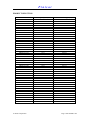
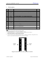
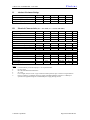
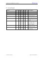
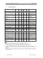
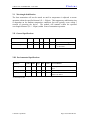
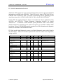
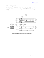
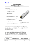
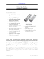
Finisar Product Specification DWDM SFP Transceiver FWLF-1631-xx PRODUCT FEATURES • Up to 2.7 Gb/s bi-directional data links • Hot-pluggable SFP footprint • Temperature-stabilized DWDMrated DFB laser transmitter • 100GHz ITU Grid, C-Band • Low dispersion DFB laser with 120km reach performance • Extended operating range: -5°C to 70°C case temperature • Amplified DWDM & SONET networks • Wavelength controlled within ± 0.1 nm over life and temperature • Bandwidth aggregation • Extended link budget with APD receiver technology • Ring topologies with fixed and reconfigurable OADMs • SONET OC-48 LR-2 compliant • Gigabit Ethernet compatible APPLICATIONS Finisar’s Dense Wavelength-Division Multiplexing (DWDM) Small Form Factor Pluggable (SFP) transceivers1 address communication network optics requirements that necessitate lower power and cost parameters. The FWLF-1631-xx is designed expressly for service providers deploying SONET and DWDM2 networking equipment in metropolitan access and core networks; and is RoHS 5-of-6 compliant per Directive 2002/95/EC3 and Finisar Application Note AN-20384. It is also compatible to Gigabit Ethernet data rate. Basic digital diagnostic features for the FWLF-1631-xx are implemented as described in Finisar Application Note AN-2030, “Digital Diagnostic Monitoring Interface for Optical Transceivers”5. Enhanced diagnostic features are available as described in the DWDM SFP MSA6. Finisar Corporation Page 1 June 2009 Rev E2 Finisar PRODUCT SELECTION Product Code FWLF-1631-17 FWLF-1631-18 FWLF-1631-19 FWLF-1631-20 FWLF-1631-21 FWLF-1631-22 FWLF-1631-23 FWLF-1631-24 FWLF-1631-25 FWLF-1631-26 FWLF-1631-27 FWLF-1631-28 FWLF-1631-29 FWLF-1631-30 FWLF-1631-31 FWLF-1631-32 FWLF-1631-33 FWLF-1631-34 FWLF-1631-35 FWLF-1631-36 FWLF-1631-37 FWLF-1631-38 FWLF-1631-39 FWLF-1631-40 FWLF-1631-41 FWLF-1631-42 FWLF-1631-43 FWLF-1631-44 FWLF-1631-45 FWLF-1631-46 FWLF-1631-47 FWLF-1631-48 FWLF-1631-49 FWLF-1631-50 FWLF-1631-51 FWLF-1631-52 FWLF-1631-53 FWLF-1631-54 FWLF-1631-55 FWLF-1631-56 FWLF-1631-57 FWLF-1631-58 FWLF-1631-59 FWLF-1631-60 FWLF-1631-61 Finisar Corporation Frequency (THz) 191.7 191.8 191.9 192.0 192.1 192.2 192.3 192.4 192.5 192.6 192.7 192.8 192.9 193.0 193.1 193.2 193.3 193.4 193.5 193.6 193.7 193.8 193.9 194.0 194.1 194.2 194.3 194.4 194.5 194.6 194.7 194.8 194.9 195.0 195.1 195.2 195.3 195.4 195.5 195.6 195.7 195.8 195.9 196.0 196.1 Center Wavelength (nm) 1563.86 1563.05 1562.23 1561.42 1560.61 1559.79 1558.98 1558.17 1557.36 1556.55 1555.75 1554.94 1554.13 1553.33 1552.52 1551.72 1550.92 1550.12 1549.32 1548.51 1547.72 1546.92 1546.12 1545.32 1544.53 1543.73 1542.94 1542.14 1541.35 1540.56 1539.77 1538.98 1538.19 1537.40 1536.61 1535.82 1535.04 1534.25 1533.47 1532.68 1531.90 1531.12 1530.33 1529.55 1528.77 Page 2 June 2009 Rev E2 Finisar FWLF-1631-xx DWDM SFP – June 2009 I. Pin Descriptions Pin 1 2 3 4 5 6 7 8 9 10 11 12 13 14 15 16 17 18 Symbol VEET TFAULT TDIS MOD_DEF(2) MOD_DEF(1) MOD_DEF(0) Rate Select LOS VEER VEER VEER RDRD+ VEER VCCR VCCT VEET TD+ 19 20 TDVEET Name/Description Transmitter Ground (Common with Receiver Ground) Transmitter Fault Transmitter Disable. Laser output disabled on high or open Module Definition 2. Data line for Serial ID Module Definition 1. Clock line for Serial ID Module Definition 0. Grounded within the module No connection required Loss of Signal indication. Logic 0 indicates normal operation Receiver Ground (Common with Transmitter Ground) Receiver Ground (Common with Transmitter Ground) Receiver Ground (Common with Transmitter Ground) Receiver Inverted DATA out. AC Coupled Receiver Non-inverted DATA out. AC Coupled Receiver Ground (Common with Transmitter Ground) Receiver Power Supply Transmitter Power Supply Transmitter Ground (Common with Receiver Ground) Transmitter Non-Inverted DATA in. 100 ohm termination between TD+ and TD-, AC Coupled thereafter Transmitter Inverted DATA in. See TD+ Transmitter Ground (Common with Receiver Ground) Ref. 1 2 3 3 3 4 5 1 1 1 1 1 1 Notes: 1. Circuit ground is internally isolated from chassis ground. 2. Laser output disabled on TDIS >2.0V or open, enabled on TDIS <0.8V. 3. Should be pulled up with 4.7k – 10kohms on host board to a voltage between 2.0V and 5.5V. MOD_DEF(0) pulls line low to indicate module is plugged in. 4. Receiver achieves multi-rate operation without active control. 5. LOS is open collector output. Should be pulled up with 4.7k – 10kohms on host board to a voltage between 2.0V and 5.5V. Logic 0 indicates normal operation; logic 1 indicates loss of signal. Towards Bezel 1 VeeT 2 TXFault 3 TX Disable 4 MOD-DEF(2) 5 MOD-DEF(1) 6 MOD-DEF(0) 7 Rate Select 8 LOS 9 VeeR 10 VeeR VeeT 20 TD- 19 TD+ 18 VeeT 17 VccT 16 VccR 15 VeeR 14 RD+ 13 RD- 12 VeeR 11 Towards ASIC Diagram of Host Board Connector Block Pin Numbers and Names Finisar Corporation Page 3 June 2009 Rev E2 Finisar FWLF-1631-xx DWDM SFP – June 2009 II. Absolute Maximum Ratings Parameter Maximum Supply Voltage Storage Temperature Case Operating Temperature III. Symbol Vcc TS TOP Min -0.5 -10 -5 Max 4.7 85 70 Unit V °C °C Electrical Characteristics (TOP = -5 to 70 °C, VCC = 3.13 to 3.50 Volts) Parameter Supply Voltage Supply Current Inrush Current Maximum Power TRANSMITTER Input differential impedance Single ended data input swing Transmit Disable Voltage Transmit Enable Voltage RECEIVER Single ended data output swing Data output rise time Data output fall time LOS Fault Vout,pp tr tf VLOS fault Vcc – 0.5 LOS Normal Power Supply Rejection VLOS norm PSR Vee 100 Notes: 1. 2. 3. 4. 5. 6. Typ Symbol Vcc Icc Isurge Pmax Rin Vin,pp VD VEN Min 3.13 Typ 3.30 Max 3.50 380 Icc+30 1 Unit V mA mA W Ref. 1200 Vcc Vee+ 0.8 Ω mV V V 1 250 Vcc – 1.3 Vee 175 1000 150 150 VccHOST mV ps ps V 3 4 4 5 Vee+0.5 V mVpp 5 6 100 2 Connected directly to TX data input pins. AC coupled thereafter. Or open circuit. Into 100 ohms differential termination. 20 – 80 % Loss of signal (LOS) is LVTTL. Logic 0 indicates normal operation; logic 1 indicates no signal detected. Receiver sensitivity is compliant with power supply sinusoidal modulation of 20 Hz to 1.5 MHz up to specified value applied through the recommended power supply filtering network. Finisar Corporation Page 4 June 2009 Rev E2 Finisar FWLF-1631-xx DWDM SFP – June 2009 IV. Low Speed Signals Parameter Symbol Min Typ Max -42 -36 -34 2 -32 RX_LOS Assert Level RX_LOS Deassert Level RX_LOS Hysteresis RX_LOS Assert Delay t_loss_on 100 RX_LOS Negate Delay t_loss_off 100 TX_DISABLE Assert Time t_off 10 TX_DISABLE Negate Time t_on 1000 TX_DISABLE Reset Time TX_FAULT Assert Finisar Corporation 0.5 t_reset 10 -0.2 +0.2 Units Notes/Conditions dBm dBm dB µsec From detection of loss of signal to assertion of RX_LOS µsec From detection of presence of signal to negation of RX_LOS µsec Rising edge of TX_DISABLE to fall of output signal below 10% of nominal Falling edge of TX_DISABLE µsec to rise of output signal above 90% of nominal. Time indicated is under steady-state temperature conditions. µsec TX_DISABLE HIGH before TX_DISABLE set LOW nm TX_Fault will assert before the device is outside of specified wavelength range Page 5 June 2009 Rev E2 Finisar FWLF-1631-xx DWDM SFP – June 2009 V. Optical Parameters Parameter Symbol Min Typ Max Units Notes/Conditions TRANSMITTER CHARACTERISTICS Center Wavelength Spacing 100 Modulated Spectral Width 0.2 0.3 nm Transmitter Center Wavelength – End of Life Transmitter Center Wavelength – Start of Life Side Mode Suppression Ratio (SMSR) Optical Rise/Fall Time Transmitter Optical Output Power ∆λ 20 λc X - 100 X X + 100 pm λc Y - 25 Y Y + 25 pm SMSR 30 tr / tf Pout 0 Transmitter Extinction Ratio Transmitter Eye Opening Transmitter Jitter (peak to peak) OMI Tolerable Back Reflection Relative Intensity Noise Dispersion Power Penalty at 2400ps/nm RECEIVER CHARACTERISTICS Optical Input Wavelength BR RIN DPP dB 160 +4 8.2 10 75 Pin -14 -120 3.0 1520 Receiver Jitter Generation Optical Input Power (BER < 10 -12) Optical Input Power – Receiver Damage Threshold Receiver Reflectance Dispersion Noise Penalty at 2400ps/nm GHz 1570 75 Pin -28 -9 +6 RRX DNP -27 3.0 Corresponds to approximately 0.8 nm Full width, -20dB from max. See note 3 X = specified ITU center wavelength Y = specified BOL center wavelength Modulated ps Unfiltered, 80% -20% dBm Average power coupled into single mode fiber dB % OC-48 eye mask margin mUI Parameter per GR-2532 section 5.6 for OC-48 B dB See note 4 dB/Hz dB See Note 5 nm Parameters per GR-2532 section 5.6 for OC-48 B dBm 2.5 Gb/s w/ PRBS 2 23 -1 dBm mUI dB dB See Note 6 Notes: 1. Parameters are specified over temperature and voltage, at end of life unless otherwise noted. 2. All parameters are measured on a Finisar SFP Evaluation Card unless otherwise noted. 3. For accurate ∆λ20 measurements, an OSA with a resolution band width of ≤ 20pm is recommended. 4. Tolerable back reflection is the max back reflection level at which the power penalty will be <1dB. 5. Dispersion power penalty is measured in loop back with OSNR set to 28 dB. Data rate and pattern used same as specified for Optical Input Power. Dispersion power penalty is the difference in Rx power at a BER of 10-12 for 0ps/nm and 2400ps/nm. 6. Dispersion noise penalty is measured in loop back with Rx power set between -9dBm and -22dBm. Data rate and pattern used same as specified for Optical Input Power. Dispersion noise penalty is the difference in OSNR at a BER of 10-12 for 0ps/nm and 2400ps/nm. Finisar Corporation Page 6 June 2009 Rev E2 Finisar FWLF-1631-xx DWDM SFP – June 2009 VI. Wavelength Stabilization The laser transmitter will not be turned on until its temperature is adjusted to ensure operation within the specified channel (X +/- 300pm). This temperature stabilization time is dependent on the ambient temperature conditions, but will typically occur within 5 seconds of powering the device. The module will transmit within the specified wavelength tolerance (X +/- 100pm) within 10 ms of transmitter operation. VII. General Specifications Parameter Data Rate Total Link Budget Symbol Min BR 0.155 28 Typ Max 2.7 30 Units Notes/Conditions Gb/sec SONET OC-3/12/48 compatible dB @ 2.5 Gb/s, BER <10-12 w/ PRBS 2-23-1. See Note 1 Note 1: Total link budget is defined as Pout – Pin – typical connector losses. VIII. Environmental Specifications Parameter Symbol Min Typ Max Units Notes/Conditions Operating Temp Top -5 70 °C Storage Temp Eye Safety Tsto -40 85 °C Case temperature measured on top-side of device Ambient temperature CDRH and IEC-825 Class 1 Laser Product. See Note 1 Note 1: Complies with FDA performance standards for laser products except for deviations pursuant to Laser Notice No. 50, dated July 26, 2001. Finisar Corporation Page 7 June 2009 Rev E2 Finisar FWLF-1631-xx DWDM SFP – June 2009 IX. Serial Communication Protocol All Finisar SFPs support the 2-wire serial communication protocol to provide module ID information as outlined in the SFP MSA1. These SFPs use an Atmel AT24C01A 128 byte E2PROM with an address of A0h. For details on interfacing with the E2PROM, see the Atmel data sheet titled “AT24C01A/02/04/08/16 2-Wire Serial CMOS E2PROM.”7 Finisar SFPs also support diagnostic features as described in Finisar Applications Note AN-20304 and SFF-84728, “Digital Diagnostic Monitoring Interface for Optical Transceivers”. A controller IC that monitors system parameters such as laser current, module temperature, transmitter power, and received power is accessible at address A2H. In addition, Finisar’s DWDM SFPs provide extended set of ID information and diagnostic features as described in the DWDM SFP MSA6. I2C clock speed, digital diagnostic accuracy and digital diagnostic range can be found in the table below. Values in the table represent the worst-case values over temperature, voltage, and life. Parameter I2C Clock Speed Accuracy Transceiver Case Temperature Transceiver Supply Voltage Tx Bias Current Tx Output Power Received Average Power Range Transceiver Case Temperature Transceiver Supply Voltage Tx Bias Current Tx Output Power Received Average Power Finisar Corporation Symbol Min Typ Max Units Notes/Conditions 0 100,000 Hz Bus can be driven blind DDTemperature -10 +10 °C Measured on the top-side of the module case DDVoltage -3 +3 % DDBias DDTxPower DDRxPower -10 -2 -2 +10 +2 +2 % dB dB DDTemperature -40 85 °C DDVoltage 3.0 4.0 V DDBias DDTxPower DDRxPower 0 -5 -30 90 +10 -7 mA dBm dBm Page 8 June 2009 Rev E2 Finisar FWLF-1631-xx DWDM SFP – June 2009 X. Mechanical Specifications Finisar’s Multi-rate DWDM Small Form Factor Pluggable (SFP) transceivers are compatible with the dimensions defined by the DWDM SFP Multi-Sourcing Agreement (MSA)6. Figure 1. DWDM SFP Outline Drawing (units in inches [mm]) Finisar Corporation Page 9 June 2009 Rev E2 FWLF-1631-xx DWDM SFP – June 2009 Finisar XI. Ordering Information Part Number FWLF-1631-xx Description DWDM SFP with APD Receiver xx = channel number (see product selection on page 2) XII. References 1. Small Form Factor Pluggable (SFP) Transceiver Multi-Source Agreement (MSA), September 2000. Documentation is currently available from Finisar upon request. 2. “SONET Transport Systems: Common Generic Criteria”, Telcordia Technologies, GR-253-CORE, Issue 3, September 2000. 3. Directive 2002/95/EC of the European Council Parliament and of the Council, “on the restriction of the use of certain hazardous substances in electrical and electronic equipment.” January 27, 2003. 4. “Application Note AN-2038: Finisar Implementation Of RoHS Compliant Transceivers”, Finisar Corporation, January 21, 2005. 5. “Application Note AN-2030: Digital Diagnostic Monitoring Interface for Optical Transceivers”, Finisar Corporation, April 2002. 6. Specifications for DWDM SFP Transceiver Draft 1.0.October 21 2005. Documentation is available from Finisar upon request. 7. “AT24C01A/02/04/08/16 2-Wire Serial CMOS E2PROM”, Atmel Corporation. www.Atmel.com. 8. “Digital Diagnostic Monitoring Interface For Optical Transceivers Rev 9.3”. SFF Document No. SFF-8472. For More Information: Finisar Corporation 1308 Moffett Park Drive Sunnyvale, CA 94089-1133 Tel. (408) 548-1000 Fax (408) 5416138 [email protected] www.finisar.com Finisar Corporation Page 10 June 2009 Rev E2