1
SUPER
C359
JP107
3
1
BUZZER RESET
JP106
JP45
JP107:OH#3 TEMP.
OPEN:45
C
1-2:50
C
2-3:55
C
C283
JP18
CH#20~23
JP45:OH#2 TEMP.
OPEN:45
C
1-2:50
C
2-3:55
C
®
A
C282
U24
CH#8~11
#11
JSM6
U73
49
U63
D36
CA
JP35
#10
JP50
C88
C
R325
BZ1
#4
C20
C149
R183
R185
R184
C136
R168
JP84:MODE
1-2:SGPIO
2-3:I2C
DESIGNED IN USA
#3
R105
C89
+
UPGRADE#1
R575
R367
JP69
C3
R624
+
Y2
C19
C229
R619
C241
C201
#2
#14
#20
C A D54
C44
JSM2
R167
U40
D53
C106
R128
R127
C198
CH#4~7
#9
C213
A
+
Y1
C135
R415
R414
R111
R112
R147
R148
R104
R344
#15
C212
C
D64
U19
C271 C272
R113
JP50:9072#2 RESET
1-2: RESET
2-3: NO RESET
JSM4
C206
D89
+
C45
CH#12~15
+
C204
A
+
JP78
C337
C
R324
+
3
R494
UPGRADE#3
JP115
#21
C329
D3
C203
+
JP97:FAN#1 SELECT
JP98:FAN#2 SELECT
JP99:FAN#3 SELECT
JP100:FAN#4 SELECT
1-2:WITH FAN
2-3:NO FAN
C199
+
+
1
JP97
JP98
JP99
JP100
+
JSM5
CA
C173
R270
R423
#16
C325
Y3
C A D51
#5
JP35:9072#1 RESET
1-2: RESET
2-3: NO RESET
1
C243
R425
R424
16
#22
C197
+
C323
+
D49
C85
1
+
CA
U2
D113
+
C327
64
D116
+
CA D47
JP25
C330
3
+
JP129
C326
+
#17
JP129:9072#3 RESET
1-2: RESET
2-3: NO RESET
D45
JP25:OH#1 TEMP.
OPEN:45
C
1-2:50
C
2-3:55
C
+
JP105
JSM3
1
#23
JSM1
+
18
22
19
23
JP96
1
JP63
JP37
I2C#1
1
JP58
6
5
3
7
#1
C5
JP10 F5
F4
C258
R305
Rev. 1.0
JP61:FAN#1 SELECT
JP62:FAN#2 SELECT
JP63:FAN#3 SELECT
JP64:FAN#4 SELECT
1-2:WITH FAN
2-3:NO FAN
REV: 1.00
MH11
#0
SAS-846A BACKPLANE
3
1
SAS846A
MH12
#12
USER'S GUIDE
4
1
JP64
+
FAN#2
MH13
FAN#4
JP60
JP26
I2C#2
4
C35
C261
JP13
4
JP46
3
1
R218
+5V
JP95
4
R220
3
JP62
C285
+5V
1
GND
JP109
C202
GND
0
1
2
F6
JP48
C194
+
+12V
MH14
#18
FAN#3
C193
C319
F19
MH15
I2C#3
F14
JP61
GND
JP52
+
F20
GND
10 11
#13
C318
4
JP110
+12V
9
+
ACT_IN#0-7
JP108
R217
JP54
8
JP47
R219
JP117
FAN#1
C328
1
+
ACT_IN#8-15
12 13 14 15
C119
20
21
R405
R404
R403
I2C#6
17
C84
R591
R629
R623
16
JP116
#19
U91
ACT_IN#16-23
I2C#5
+
CH#0~3
C200
C324
+
SAS-846A Backplane User's Guide
The information in this User’s Manual has been carefully reviewed and is believed to be accurate.
The vendor assumes no responsibility for any inaccuracies that may be contained in this document,
makes no commitment to update or to keep current the information in this manual, or to notify any
person or organization of the updates. Please Note: For the most up-to-date version of this
manual, please see our web site at www.supermicro.com.
Super Micro Computer, Inc. ("Supermicro") reserves the right to make changes to the product
described in this manual at any time and without notice. This product, including software, if any,
and documentation may not, in whole or in part, be copied, photocopied, reproduced, translated or
reduced to any medium or machine without prior written consent.
IN NO EVENT WILL SUPERMICRO BE LIABLE FOR DIRECT, INDIRECT, SPECIAL, INCIDENTAL,
SPECULATIVE OR CONSEQUENTIAL DAMAGES ARISING FROM THE USE OR INABILITY TO
USE THIS PRODUCT OR DOCUMENTATION, EVEN IF ADVISED OF THE POSSIBILITY OF
SUCH DAMAGES. IN PARTICULAR, SUPERMICRO SHALL NOT HAVE LIABILITY FOR ANY
HARDWARE, SOFTWARE, OR DATA STORED OR USED WITH THE PRODUCT, INCLUDING THE
COSTS OF REPAIRING, REPLACING, INTEGRATING, INSTALLING OR RECOVERING SUCH
HARDWARE, SOFTWARE, OR DATA.
Any disputes arising between manufacturer and customer shall be governed by the laws of Santa
Clara County in the State of California, USA. The State of California, County of Santa Clara shall
be the exclusive venue for the resolution of any such disputes. Super Micro's total liability for
all claims will not exceed the price paid for the hardware product.
FCC Statement: This equipment has been tested and found to comply with the limits for a Class
A digital device pursuant to Part 15 of the FCC Rules. These limits are designed to provide
reasonable protection against harmful interference when the equipment is operated in a commercial
environment. This equipment generates, uses, and can radiate radio frequency energy and, if not
installed and used in accordance with the manufacturer’s instruction manual, may cause harmful
interference with radio communications. Operation of this equipment in a residential area is likely
to cause harmful interference, in which case you will be required to correct the interference at your
own expense.
California Best Management Practices Regulations for Perchlorate Materials: This Perchlorate
warning applies only to products containing CR (Manganese Dioxide) Lithium coin cells. “Perchlorate
Material-special handling may apply. See www.dtsc.ca.gov/hazardouswaste/perchlorate”
WARNING: Handling of lead solder materials used in this
product may expose you to lead, a chemical known to
the State of California to cause birth defects and other
reproductive harm.
Manual Revision 1.0
Release Date: December 10, 2008
Unless you request and receive written permission from Super Micro Computer, Inc., you may not
copy any part of this document.
Information in this document is subject to change without notice. Other products and companies
referred to herein are trademarks or registered trademarks of their respective companies or mark
holders.
Copyright © 2008 by Super Micro Computer, Inc.
All rights reserved.
Printed in the United States of America
ii
Preface
Table of Contents
Contacting Supermicro........................................................................................iv
Returning Merchandise for Service.....................................................................v
Chapter 1 Safety Guidelines
1-1
ESD Safety Guidelines.................................................................................... 1-1
1-2
General Safety Guidelines............................................................................... 1-1
1-3
A Note to Users................................................................................................ 1-2
Chapter 2 Jumper Settings and Pin Definitions
2-1
Front Connectors and Jumpers....................................................................... 2-1
Front Connectors and Components................................................................. 2-1
2-2
Front Connector and Pin Definitions................................................................ 2-2
2-3
Front Jumper Locations and Pin Definitions.................................................... 2-3
Fan Jumper Settings........................................................................................ 2-4
I2C and SGPIO Modes and Jumper Settings.................................................. 2-4
Front LED Indicators........................................................................................ 2-5
2-4
Rear Connectors and LED Indicators.............................................................. 2-6
iii
SAS-846A Backplane User's Guide
Contacting Supermicro
Headquarters
Address:
Super Micro Computer, Inc.
980 Rock Ave.
San Jose, CA 95131 U.S.A.
Tel:
+1 (408) 503-8000
Fax:
+1 (408) 503-8008
Email:
[email protected] (General Information)
[email protected] (Technical Support)
Web Site:
www.supermicro.com
Europe
Address:
Super Micro Computer B.V.
Het Sterrenbeeld 28, 5215 ML
's-Hertogenbosch, The Netherlands
Tel:
+31 (0) 73-6400390
Fax:
+31 (0) 73-6416525
Email:
[email protected] (General Information)
[email protected] (Technical Support)
[email protected] (Customer Support)
Asia-Pacific
Address:
Super Micro Computer, Inc.
4F, No. 232-1, Liancheng Rd.
Chung-Ho 235, Taipei County
Taiwan, R.O.C.
Tel:
+886-(2) 8226-3990
Fax:
+886-(2) 8226-3991
Web Site:
www.supermicro.com.tw
Technical Support:
Email:
[email protected]
Tel: 886-2-8226-1900
iv
Preface
Returning Merchandise for Service
A receipt or copy of your invoice marked with the date of purchase is required before any warranty service will be rendered. You can obtain service by calling your
vendor for a Returned Merchandise Authorization (RMA) number. When returning
to the manufacturer, the RMA number should be prominently displayed on the
outside of the shipping carton, and mailed prepaid or hand-carried. Shipping and
handling charges will be applied for all orders that must be mailed when service
is complete.
For faster service, RMA authorizations may be requested online (http://www.supermicro.com/support/rma/).
Whenever possible, repack the backplane in the original Supermicro box, using the
original packaging materials. If these are no longer available, be sure to pack the
backplane in an anti-static bag and inside the box. Make sure that there is enough
packaging material surrounding the backplane so that it does not become damaged
during shipping.
This warranty only covers normal consumer use and does not cover damages incurred in shipping or from failure due to the alteration, misuse, abuse or improper
maintenance of products.
During the warranty period, contact your distributor first for any product problems.
v
SAS-846A Backplane User's Guide
Notes
vi
Chapter 1: Safety Guidelines
Chapter 1
Safety Guidelines
To avoid personal injury and property damage, carefully follow all the safety steps
listed below when accessing your system or handling the components.
1-1 ESD Safety Guidelines
Electrostatic Discharge (ESD) can damage electronic components. To prevent damage to your system, it is important to handle it very carefully. The following measures
are generally sufficient to protect your equipment from ESD.
•Use a grounded wrist strap designed to prevent static discharge.
•Touch a grounded metal object before removing a component from the antistatic
bag.
•Handle the RAID card by its edges only; do not touch its components, peripheral
chips, memory modules or gold contacts.
•When handling chips or modules, avoid touching their pins.
•Put the card and peripherals back into their antistatic bags when not in use.
1-2 General Safety Guidelines
•Always disconnect power cables before installing or removing any components
from the computer, including the backplane.
•Disconnect the power cable before installing or removing any cables from the
backplane.
•Make sure that the backplane is securely and properly installed on the motherboard to prevent damage to the system due to power shortage.
1-1
SAS-846A Backplane User's Guide
1-3 A Note to Users
•All images and layouts shown in this user's guide are based upon the latest PCB
Revision available at the time of publishing. The card you have received may or
may not look exactly the same as the graphics shown in this manual.
1-2
Chapter 2: Jumper Settings and Pin Definitions
Chapter 2
Jumper Settings and Pin Definitions
2-1 Front Connectors and Jumpers
13
1
C359
C283
JP18
CH#20~23
JP106
U24
JSM6
D89
C
A
D53
C A D54
C
R325
BZ1
+
C85
D64
18
C106
R128
R127
C44
C20
C149
R183
R185
R184
C136
R168
UPGRADE#1
DESIGNED IN USA
#3
C3
JP69
C19
#2
JSM1
CH#0~3
+
C119
13
R405
R404
R403
ACT_IN#0-7
JP63
C194
JP37
4
JP95
2
6
3
7
JP26
I2C#2
4
#1
17
3
R220
JP10 F5
C5
17
MH12
4
1
1
FAN#2
MH13
FAN#4
JP60
JP64
+
C35
C261
JP13
17
JP58
5
F6
1
JP46
R218
C258
17
R305
17
#12
4
CA
+
12
FAN#3
C193
I2C#1
1
D36
JP84:MODE
1-2:SGPIO
2-3:I2C
0
1
+
JP62
A
#4
I2C#3
3
+5V
+5V
MH14
#18
JP47
JP52
R219
C319
GND
3
MH15
10 11
C285
GND
1
GND
+12V
JP109
GND
9
+
F20
C202
+12V
8
+
ACT_IN#8-15
12 13 14 15
R367
1
4
JP110
R624
14
C201
JP48
JP54
U91
JP96
#13
C318
F19
1
JSM2
+
C241
F14
R217
JP61
15
JP108
FAN#1
C328
+
CH#4~7
R167
23
C
+
Y1
C135
22
19
C88
C84
JP117
20
21
18
R415
R414
R111
R112
R147
R148
R104
R344
19
C198
#19
17
3
C200
+
ACT_IN#16-23
16
1
R591
R629
R623
13
I2C#6
D3
R105
C89
12
R619
CA
U19
C271 C272
R113
JP50:9072#2 RESET
1-2: RESET
2-3: NO RESET
+
Y2
13
#14
I2C#5
#10
JP50
R575
C204
JP116
U40
C A D51
C173
C324
+
C213
D49
+
#9
C212
CA
R324
C45
#15
C206
CA D47
+
JSM4
C229
#20
JP35
D45
#5
JP78
C337
JP97
JP98
JP99
JP100
+
A
JP25:OH#1 TEMP.
OPEN:45
C
1-2:50
C
2-3:55
C
C203
CH#12~15
+
16
1
+
JP105
JSM3
JP35:9072#1 RESET
1-2: RESET
2-3: NO RESET
1
R494
UPGRADE#3
JP115
#21
C329
R270
#16
JP97:FAN#1 SELECT
JP98:FAN#2 SELECT
JP99:FAN#3 SELECT
JP100:FAN#4 SELECT
1-2:WITH FAN
2-3:NO FAN
C199
+
11
1
C243
JSM5
R423
12
+
Y3
1
U63
C323
16
C197
+
R425
R424
12
1
#22
C325
+
+
49
1
+
CH#8~11
U2
D113
+
C327
D116
U73
10
1
C282
3
64
JP45:OH#2 TEMP.
OPEN:45
C
1-2:50
C
2-3:55
C
#17
JP129:9072#3 RESET
1-2: RESET
2-3: NO RESET
JP25
C330
+
JP45
JP107:OH#3 TEMP.
OPEN:45
C
1-2:50
C
2-3:55
C
#11
JP129
C326
+
JP107
3
1
1
1
BUZZER RESET
#23
17
F4
SAS846A
MH11
#0
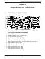
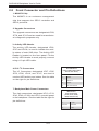
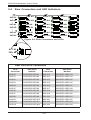
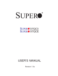
Figure 2-1: Front Components
Front Connectors and Components
1. Chip: MG9072
2. Upgrade Connectors: JP69, JP78 and JP115
3. ACT_IN: JP26, JP47, and JP108
4. I2C Connector #1 (JP37) and #2 (JP95)
5. I2C Connector #3 (JP52) and #4 (JP96)
6. I2C Connector #5 (JP116) and #6 (JP117)
7. Power Connectors (4-pin): JP10, JP13, JP46, JP48, JP109, and JP110
8. IPASS Connector CH# 0-3, JSM1
9. IPASS Connector CH# 4-7, JSM2
10. IPASS Connector CH# 8-11, JSM3
11. IPASS Connector CH# 12-15, JSM4
12. IPASS Connector CH# 16-19, JSM5
13. IPASS Connector CH# 20-23, JSM6
2-1
JP61:FAN#1 SELECT
JP62:FAN#2 SELECT
JP63:FAN#3 SELECT
JP64:FAN#4 SELECT
1-2:WITH FAN
2-3:NO FAN
REV: 1.00
SAS-846A Backplane User's Guide
2-2 Front Connector and Pin Definitions
1. MG9072 Chip
The MG9072 is an enclosure management
chip that supports the SES-2 controller and
SES-2 protocols.
2. Upgrade Connectors
The upgrade connectors are designated JP69,
JP78, and JP115 and are used for manufacturer's diagnostic purposes only.
3. Activity LED Header
The activity LED header, designated JP26,
JP47 and JP108, is used to indicate the activity status of each SAS drive. The Activity LED
Header is located on the front panel. For the
Activity LED Header to work properly, connect
using a 10-pin LED cable.
4./5./6. I2C Connectors
The I2C Connectors, designated JP37, JP95,
JP52, JP96, JP116, and JP117, are used to
monitor HDD activity and status. See the table
on the right for pin definitions.
I2C Connector
Pin Definitions
(JP37, JP95, JP52, JP96,
JP116, and JP117)
Pin# Definition 1
Data
2
Ground
3
Clock
4
No Connection
7. Backplane Main Power Connectors
The 4-pin connectors, designated JP10, JP13,
JP46, JP48, JP109, and JP110, provide power
to the backplane. See the table on the right for
pin definitions.
2-2
Backplane
Main Power
4-Pin Connector
(JP10, JP13, JP46,
JP48, 109 and 110)
Pin# Definition 1
+12V
2 and 3
Ground
4
+5V
Chapter 2: Jumper Settings and Pin Definitions
2-3 Front Jumper Locations and Pin Definitions
JP18
JP129
C359
BUZZER RESET
C283
JP18
CH#20~23
JP106
U24
JP107
3
1
JSM6
U73
49
1
3
JP35
JP50
JP50
#10
C88
C
A
D36
CA
D89
C
A
C A D54
C
R325
BZ1
#4
+
C44
C20
C149
R183
R185
R184
R167
C136
R168
JP84:MODE
1-2:SGPIO
2-3:I2C
DESIGNED IN USA
#3
R105
C89
+
UPGRADE#1
R575
R367
JP69
C3
R624
C19
C229
R619
C241
C201
#2
#14
#20
D53
D64
JP84
CH#4~7
JSM2
+
Y2
C204
D3
C106
R128
R127
Y1
C135
R415
R414
R111
R112
R147
R148
R104
R344
C198
U40
CA
+
#9
C213
C A D51
U19
C271 C272
R113
JP50:9072#2 RESET
1-2: RESET
2-3: NO RESET
+
#15
C212
D49
+
C45
JSM4
C206
CA
R324
+
CH#12~15
+
CA D47
#5
JP78
C337
1
R494
UPGRADE#3
JP115
#21
C329
+
C173
C199
1
JP97
JP98
JP99
JP100
JP35
JP97:FAN#1 SELECT
JP98:FAN#2 SELECT
JP99:FAN#3 SELECT
JP100:FAN#4 SELECT
1-2:WITH FAN
2-3:NO FAN
JSM5
+
JP35:9072#1 RESET
1-2: RESET
2-3: NO RESET
R270
R423
#16
+
Y3
D45
JP25:OH#1 TEMP.
OPEN:45
C
1-2:50
C
2-3:55
C
+
JP105
JSM3
C203
C197
+
C243
16
#22
C325
+
A
C282
CH#8~11
#11
U63
C323
R425
R424
+
JP45:OH#2 TEMP.
OPEN:45
C
1-2:50
C
2-3:55
C
C85
D113
+
C327
64
D116
+
JP45
U2
C330
3
+
JP129
C326
+
#17
JP129:9072#3 RESET
1-2: RESET
2-3: NO RESET
JP25
1
#23
JP97
JP98
JP99
JP100
JP107:OH#3 TEMP.
OPEN:45
C
1-2:50
C
2-3:55
C
JSM1
+
18
22
19
23
JP96
JP37
6
7
#1
4
1
JP64
3
1
R220
+
C5
JP63
FAN#4
JP60
JP26
JP13
MH13
JP62
2
3
I2C#2
4
C35
C261
JP10 F5
JP46
FAN#2
JP58
5
F6
3
4
C258
R305
#12
1
R218
3
MH14
JP95
I2C#1
1
JP62
C285
+5V
1
GND
JP109
C202
GND
+5V
#18
JP63
C194
1
JP48
F19
JP61
GND
FAN#3
C193
C319
+
+12V
4
0
1
I2C#3
+
F20
GND
JP47
JP52
#13
C318
4
JP110
+12V
10 11
F14
JP61
JP54
9
ACT_IN#0-7
JP108
R217
1
8
+
R219
JP117
FAN#1
C328
+
+
ACT_IN#8-15
12 13 14 15
C119
20
21
R405
R404
R403
I2C#6
17
C84
R591
R629
R623
16
JP116
#19
U91
ACT_IN#16-23
I2C#5
MH15
CH#0~3
C200
C324
+
F4
SAS846A
JP61:FAN#1 SELECT
JP62:FAN#2 SELECT
JP63:FAN#3 SELECT
JP64:FAN#4 SELECT
1-2:WITH FAN
2-3:NO FAN
JP64
MH12
REV: 1.00
MH11
#0
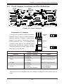
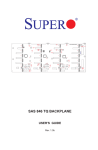
Figure 2-2: Front Jumpers
Explanation of Jumpers
To modify the operation of the backplane,
jumpers can be used to choose between
optional settings. Jumpers create shorts
between two pins to change the function
of the connector. Pin 1 is identified with
a square solder pad on the printed circuit
board. Note: On two pin jumpers, "Closed"
means the jumper is on and "Open" means
the jumper is off the pins.
Connector
Pins
3
2
1
3
2
1
Jumper
Setting
Jumper Settings
Jumper
Jumper Setting
Notes
JP35
1-2: Reset
2-3: Default
MG9072 Chip Reset #1
JP50
1-2: Reset
2-3: Default
MG9072 Chip Reset #2
JP129
1-2: Reset
2-3: Default
MG9072 Chip Reset #3
JP18
1-2: Reset
2-3: Not reset (Default)
Buzzer disabled*
Buzzer enabled*
*The buzzer sound indicates that an overheat condition or drive failure has occured.
2-3
SAS-846A Backplane User's Guide
Fan Jumper Settings
This backplane can use up to four fans. To utilize each fan, you must configure
both jumpers as indicated below.
Fan Jumper Settings
Jumper
Jumper Settings
Note
JP61
1-2:With Fan (Default)
2-3:No Fan
FAN#1
JP97
1-2:With Fan (Default)
2-3:No Fan
FAN#1
JP62
1-2:With Fan (Default)
2-3:No Fan
FAN#2
JP98
1-2:With Fan (Default)
2-3:No Fan
FAN#2
JP63
1-2:With Fan (Default)
2-3:No Fan
FAN#3
JP99
1-2:With Fan (Default)
2-3:No Fan
FAN#3
JP64
1-2:With Fan (Default)
2-3:No Fan
FAN#4
JP100
1-2:With Fan (Default)
2-3:No Fan
FAN#4
I2C and SGPIO Modes and Jumper Settings
This backplane can utilize I2C or SGPIO. SGPIO is the default mode and can be
used without making changes to your jumper. The following information details
which jumper must be configured to use SGPIO mode or restore your backplane
to I2C mode.
SGPIO Setting (Default)
Jumper
JP84
SGPIO Jumper Setting (Default)
1-2
I2C Jumper Setting
2-3
2-4
Chapter 2: Jumper Settings and Pin Definitions
Front LED Indicators
A
D45
CA D47
D49
CA
C A D51
C
D3
CA
D36
A
D89
CA
C
A
JP25:OH#1 TEMP.
OPEN:45
C
1-2:50
C
2-3:55
C
+
JP25
U2
C359
BUZZER RESET
C283
JP18
CH#20~23
JP106
JP107
3
1
JP45
JP107:OH#3 TEMP.
OPEN:45
C
1-2:50
C
2-3:55
C
JP45:OH#2 TEMP.
OPEN:45
C
1-2:50
C
2-3:55
C
A
C282
U24
CH#8~11
#11
JSM6
U73
+
+
49
C323
1
1
A
D36
CA
JP35
#10
JP50
C88
R325
BZ1
#4
C20
C149
R183
R185
R184
R167
C136
R168
JP84:MODE
1-2:SGPIO
2-3:I2C
DESIGNED IN USA
#3
R105
C89
+
UPGRADE#1
R575
R624
R367
JP69
C3
D64
+
C19
R619
C241
#5
C
D64
C201
#2
#14
#20
C A D54
C44
JSM2
C85
C229
C45
U40
D53
C106
R128
R127
C198
CH#4~7
#9
C213
Y2
A
+
Y1
C135
R415
R414
R111
R112
R147
R148
R104
R344
#15
C212
C
+
U19
C271 C272
R113
JP50:9072#2 RESET
1-2: RESET
2-3: NO RESET
+
JSM4
C206
D89
+
C45
CH#12~15
+
C204
C
R324
+
3
JP97
JP98
JP99
JP100
+
JP78
C337
D3
C173
R494
UPGRADE#3
JP115
#21
CA
#5
JP35:9072#1 RESET
1-2: RESET
2-3: NO RESET
R270
R423
C199
C329
C243
#16
JP97:FAN#1 SELECT
JP98:FAN#2 SELECT
JP99:FAN#3 SELECT
JP100:FAN#4 SELECT
1-2:WITH FAN
2-3:NO FAN
JSM5
+
+
R425
R424
+
Y3
C A D51
C203
C197
+
U63
+
16
#22
C325
+
D49
C85
1
+
CA
U2
D113
C327
64
D116
CA D47
JP25
C330
3
+
JP129
C326
+
#17
JP129:9072#3 RESET
1-2: RESET
2-3: NO RESET
D45
JP25:OH#1 TEMP.
OPEN:45
C
1-2:50
C
2-3:55
C
+
JP105
JSM3
1
#23
JSM1
CH#0~3
C200
C324
+
+
18
22
19
23
JP96
F14
4
6
5
3
7
#1
4
1
F6
JP64
3
1
R220
3
+
C5
JP13
JP10 F5
JP46
FAN#2
C258
R305
MH13
FAN#4
JP60
JP26
I2C#2
4
C35
C261
F4
SAS846A
JP61:FAN#1 SELECT
JP62:FAN#2 SELECT
JP63:FAN#3 SELECT
JP64:FAN#4 SELECT
1-2:WITH FAN
2-3:NO FAN
REV: 1.00
#4
MH11
MH12
#0
#12
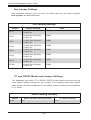
Figure 2-3: Front LEDs
C106
R128
R127
+
C135
CH#4~7
State
On
C149
R183
R185
R184
JP84:MODE
On
1-2:SGPIO
2-3:I2C
C136
R168
D51
D3
D89
Failure in Fan #3
On
Alarm #1: Overheat/Drive Failure in Channel 1
+On
Alarm #2: Overheat/Drive Failure in Channel 2
On
Alarm #3: Overheat/Drive Failure in Channel 3
JP69
Off
D54
Off
+12V : Backplane power failure. Light is on
#2
during normal operation.
+
C119
R405
R404
R403
4
#3
+5V : Backplane power failure. Light is on
during normal operation.
C19
D53
0
DES
Failure in Fan #4
C3
R624
Failure in Fan #1
On
R105
C89
UPGRADE#1
D36
Spefication
Failure in Fan #2
C20
On
D47
R167
D45
C44
LED
D49
R367
4
1
JP58
0
1
2
Front Panel LEDs
Y1
JSM2
R575
JP95
I2C#1
R218
3
MH14
U19
C271 C272
C88
JP37
1
JP62
C285
+5V
1
GND
#18
R415
R414
R111
R112
R147
R148
R104
R344
JP63
C194
1
JP48
GND
JP109
+12V
+5V
MH15
R113
FAN#3
C193
+
C202
GND
I2C#3
C319
F19
GND
JP52
+
F20
JP110
+12V
10 11
#13
C318
4
JP54
9
+
ACT_IN#0-7
JP108
R217
JP61
1
8
JP47
R219
JP117
FAN#1
C328
+
+
ACT_IN#8-15
12 13 14 15
C119
I2C#6
20
21
R405
R404
R403
JP116
17
C84
R591
R629
R623
16
I2C#5
#19
U91
ACT_IN#16-23
2-5
ACT#9
ACT#3
C
D15
D8
R180
R90
FAIL#3
FAIL#9
AC
R88
A
2-4 Rear Connectors and LED Indicators
SAS
C
ACT#23
AC
ACT#8
A D121
R514
FAIL#23
D118 C
FAIL#8
A D119
R511
FAIL#22
C368
C365
R109
D106 C
R463
ACT#20
D42
AC
AC
R253
ACT#14
SAS
J33
Q35
A D109
R466
FAIL#20
FAIL#14
A
R215
D39
#20
AC
J37
A D108
R465
R178
SAS
FAIL#19
A
R214
D38
FAIL#13
AC
R251
D41
ACT#19
D104 C
R461
C
ACT#13
A
ACT#18
D102 C
R460
D40
AC
AC
R250
AC
R164
D22
J35
SAS
A D107
R464
FAIL#18
R91
R92
A
R213
A
A
FAIL#12
D37
R165
FAIL#6
D23
R85
D5
FAIL#0
ACT#7
#19
C
ACT#12
C
ACT#6
AC
#18
FAIL#7
R173
SAS #18
J21
A D110
R467
FAIL#21
J43
#21
C
D29
FAIL#7
R173
AC
R83
D12
SAS
#12
R179
AC
A
R435
D24
C
ACT#0
SAS #19
J27
#13
R468
ACT#21
D88
FAIL#15
AC
R428
C
ACT#7
SAS
D87
R109
#8
D111 C
C
ACT#15
A
R179
D30
SAS #20
J28
SAS
#14
SAS
R174
AC
ACT#22
J45
R510
A
R459
AC
FAIL#8
A
R87
C75
FAIL#1
D6
AC
R84
SAS #12
D120
R512
FAIL#16
J17
D25
R174
D13
J13
D103
AC
SAS
C75
C
ACT#1
SAS
#6
R457
J31
SAS
#15
C
ACT#8
A
R89
D7
FAIL#2
SAS #6
SAS #21
A
R180
AC
R86
D14
SAS #13
J15
SAS
#22
R178
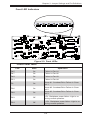
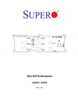
Figure 2-4: Rear Connectors and
LEDs
SAS
A
R87
FAIL#1
D6
AC
Q14
SAS
#7
J44
D100
D31
FAIL#9
AC
R175
D26
ACT#9
C
ACT#2
SAS #14
#8
#16
C
A
R90
J17
A
R181
FAIL#3
D8
SAS #15
J18
SAS #22
J34
SAS
#23
C
ACT#16
FAIL#10
AC
R88
SAS
D32
AC
R176
D15
SAS
#9
SAS
A
D27
J19
C
ACT#3
J1
FAIL#17
#17
D105
J36
C
ACT#10
A
R96
SAS #16
D19
SAS
#10
R458 R462
SAS
D101
AC
ACT#17
R182
FAIL#4
AC
REV: 1.00
SAS
#0
SAS #23
A
FAIL#11
R95
SAS #7
D13
SAS846A
R84
Q13
Q14
#1
C
SAS #0
Q13
J2
SAS
ACT#1
SAS #1
C
D33
AC
R177
ACT#11
D28
#11
D18
ACT#4
SAS #8
J3
SAS
#2
J20
C
SAS #2
A
R149
#3
SAS #17
D20
FAIL#5
D7
A
R89
FAIL#2
SAS #9
J4
SAS
D21
AC
R150
ACT#5
SAS #10
#4
SAS
J18
#9
C
C
D14
J9
AC
SAS
R86
SAS #3
#5
C
SAS #4
ACT#2
SAS #5
SAS #11
J11
SAS
R175
SAS-846A Backplane User's Guide
J15
#7
ACT#6
C
AC
R164
D12
R83
A
R92
R91
SAS
J13
#6
Rear SAS/SATA Connectors
Rear
Connector
SAS Drive
Number
Rear
Connector
SAS Drive
Number
SAS #0
SAS/SATA HDD #1
SAS #12
SAS/SATA HDD #13
SAS #1
SAS/SATA HDD #2
SAS #13
SAS/SATA HDD #14
SAS #2
SAS/SATA HDD #3
SAS #14
SAS/SATA HDD #15
SAS #3
SAS/SATA HDD #4
SAS #15
SAS/SATA HDD #16
SAS #4
SAS/SATA HDD #5
SAS #16
SAS/SATA HDD #17
SAS #5
SAS/SATA HDD #6
SAS #17
SAS/SATA HDD #18
SAS #6
SAS/SATA HDD #7
SAS #18
SAS/SATA HDD #19
SAS #7
SAS/SATA HDD #8
SAS #19
SAS/SATA HDD #20
SAS #8
SAS/SATA HDD #9
SAS #20
SAS/SATA HDD #21
SAS #9
SAS/SATA HDD #10
SAS #21
SAS/SATA HDD #22
SAS #10
SAS/SATA HDD #11
SAS #22
SAS/SATA HDD #23
SAS #11
SAS/SATA HDD #12
SAS #23
SAS/SATA HDD #24
2-6
R165
FAIL#6
R85
D5
FAIL#0
FAIL #0
ACT#0
ACT #0
Chapter 2: Jumper Settings and Pin Definitions
Rear LED Indicators
Hard Drive Activity
Failure LED
SAS #0
Rear LED
D12
D5
SAS #1
D13
D6
SAS #2
D14
D7
SAS #3
D15
D8
SAS #4
D18
D19
SAS #5
D21
D20
SAS #6
D22
D23
SAS #7
D24
D29
SAS #8
D25
D30
SAS #9
D26
D31
SAS #10
D27
D32
SAS #11
D28
D33
SAS #12
D40
D37
SAS #13
D41
D38
SAS #14
D42
D39
SAS #15
D87
D88
SAS #16
D100
D103
SAS #17
D101
D105
SAS #18
D102
D107
SAS #19
D104
D108
SAS #20
D106
D109
SAS #21
D111
D110
SAS #22
D118
D119
SAS #23
D120
D121
2-7
SAS-846A Backplane User's Guide
Disclaimer (cont.)
The products sold by Supermicro are not intended for and will not be used in life support systems, medical equipment, nuclear facilities or systems, aircraft, aircraft devices,
aircraft/emergency communication devices or other critical systems whose failure to perform be reasonably expected to result in significant injury or loss of life or catastrophic
property damage. Accordingly, Supermicro disclaims any and all liability, and should
buyer use or sell such products for use in such ultra-hazardous applications, it does so
entirely at its own risk. Furthermore, buyer agrees to fully indemnify, defend and hold
Supermicro harmless for and against any and all claims, demands, actions, litigation,
and proceedings of any kind arising out of or related to such ultra-hazardous use or
sale.
2-8