1
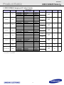
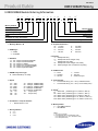
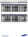
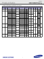
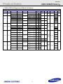
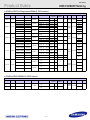
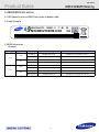
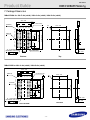
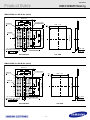
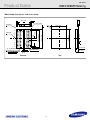
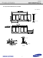
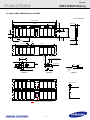
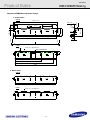
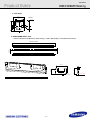
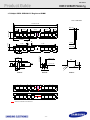
Jan. 2011
DDR3 SDRAM Memory
Product Guide
SAMSUNG ELECTRONICS RESERVES THE RIGHT TO CHANGE PRODUCTS, INFORMATION AND
SPECIFICATIONS WITHOUT NOTICE.
Products and specifications discussed herein are for reference purposes only. All information discussed
herein is provided on an "AS IS" basis, without warranties of any kind.
This document and all information discussed herein remain the sole and exclusive property of Samsung
Electronics. No license of any patent, copyright, mask work, trademark or any other intellectual property
right is granted by one party to the other party under this document, by implication, estoppel or otherwise.
Samsung products are not intended for use in life support, critical care, medical, safety equipment, or
similar applications where product failure could result in loss of life or personal or physical harm, or any
military or defense application, or any governmental procurement to which special terms or provisions
may apply.
For updates or additional information about Samsung products, contact your nearest Samsung office.
All brand names, trademarks and registered trademarks belong to their respective owners.
ⓒ 2011 Samsung Electronics Co., Ltd. All rights reserved.
-1-
Jan. 2011
Product Guide
DDR3 SDRAM Memory
1. DDR3 SDRAM MEMORY ORDERING INFORMATION
1
2
3
4
5
6
7
8
9
10
11
K 4 B X X X X X X X - X X X X
Speed
SAMSUNG Memory
DRAM
Temp & Power
DRAM Type
Package Type
Density
Revision
Interface (VDD, VDDQ)
Bit Organization
# of Internal Banks
1. SAMSUNG Memory : K
7. Interface ( VDD, VDDQ)
6 : SSTL (1.5V, 1.5V)
2. DRAM : 4
8. Revision
M
A
B
C
D
E
F
G
H
3. DRAM Type
B : DDR3 SDRAM
4. Density
51 : 512Mb
1G :
1Gb
2G :
2Gb
4G :
4Gb
: 1st Gen.
: 2nd Gen.
: 3rd Gen.
: 4th Gen.
: 5th Gen.
: 6th Gen.
: 7th Gen.
: 8th Gen.
: 9th Gen.
9. Package Type
Z
H
J
M
B
5. Bit Organization
04 : x 4
08 : x 8
16 : x16
:
:
:
:
:
FBGA (Lead-free)
FBGA (Halogen-free & Lead-free)
FBGA (Lead-free, DDP)
FBGA (Halogen-free & Lead-free, DDP)
FBGA (Halogen-free & Lead-free, Flip Chip)
10. Temp & Power
C : Commercial Temp.( 0°C ~ 85°C) & Normal Power
Y : Commercial Temp.( 0°C ~ 85°C) & Low VDD(1.35V)
6. # of Internal Banks
3 : 4 Banks
4 : 8 Banks
5 : 16 Banks
11. Speed
F7 : DDR3-800
F8 : DDR3-1066
H9 : DDR3-1333
K0 : DDR3-1600
MA : DDR3-1866
-2-
(400MHz @ CL=6, tRCD=6, tRP=6)
(533MHz @ CL=7, tRCD=7, tRP=7)
(667MHz @ CL=9, tRCD=9, tRP=9)
(800MHz @ CL=11, tRCD=11, tRP=11)
(933MHz @ CL=13, tRCD=13, tRP=13)
Jan. 2011
Product Guide
DDR3 SDRAM Memory
2. DDR3 SDRAM Component Product Guide
Density
1Gb F-die
1Gb G-die
2Gb C-die
2Gb D-die
4Gb A-die
4Gb B-die
DDP 4Gb C-die
DDP 4Gb D-die
Banks
8Banks
8Banks
8Banks
8Banks
8Banks
8Banks
8Banks
8Banks
Part Number
Package & Power,
Temp. & Speed
Org.
K4B1G0446F
HCF8/H9/K0
256M x 4
K4B1G0846F
HCF8/H9/K0
128M x 8
K4B1G0446F
HYF8/H9
256M x 4
K4B1G0846F
HYF8/H9
128M x 8
K4B1G0446G
BCF8/H9/K0/MA
256M x 4
K4B1G0846G
BCF8/H9/K0/MA
128M x 8
K4B1G0446G
BYF8/H9/K0
256M x 4
K4B1G0846G
BYF8/H9/K0
128M x 8
K4B2G0446C
HCF8/H9/K0
512M x 4
K4B2G0846C
HCF8/H9/K0
256M x 8
K4B2G0446C
HYF8/H9
512M x 4
K4B2G0846C
HYF8/H9
256M x 8
K4B2G0446D
HCF8/H9/K0/MA
512M x 4
K4B2G0846D
HCF8/H9/K0/MA
256M x 8
K4B2G0446D
HYF8/H9/K0
512M x 4
K4B2G0846D
HYF8/H9/K0
256M x 8
K4B4G0446A
HCF8/H9/K0
1G x 4
K4B4G0846A
HCF8/H9/K0
512M x 8
K4B4G0446A
HYF8/H9/K0
1G x 4
K4B4G0846A
HYF8/H9/K0
512M x 8
K4B4G0446B
HCF8/H9/K0/MA
1G x 4
K4B4G0846B
HCF8/H9/K0/MA
512M x 8
K4B4G0446B
HYF8/H9/K0
1G x 4
512M x 8
K4B4G0846B
HYF8/H9/K0
K4B4G0446C
MCF7/F8/H9
1G x 4
K4B4G0846C
MCF7/F8/H9
512M x 8
K4B4G0446D
MCF8/H9/K0/MA
K4B4G0846D
MCF8/H9/K0
512M x 8
1G x 4
K4B4G0446D
MYF8/H9/K0
1G x 4
K4B4G0846D
MYF8/H9/K0
512M x 8
* NOTE
1. 1.35V product is 1.5V operatable.
-3-
VDD Voltage1
PKG
Avail.
78 ball
FBGA
Now
78 ball
FBGA
Now
78 ball
FBGA
Now
78 ball
FBGA
Now
1.5V
1.35V
1.5V
1.35V
1.5V
1.35V
1.5V
1.35V
1.5V
78 ball
FBGA
Now
78 ball
FBGA
3Q’11
1.35V
1.5V
1.35V
1.5V
78 ball
FBGA
Now
78 ball
FBGA
2Q’11
1.5V
1.35V
NOTE
Jan. 2011
Product Guide
DDR3 SDRAM Memory
3. DDR3 SDRAM Module Ordering Information
1
2
3
4
5
6
7
8
9
10
11
131
12
M X X X B X X X X X X X - X X X X
Memory Module
DIMM Type
Data bits
Memory Buffer
Speed
DRAM Component Type
Temp & Power
Depth
PCB Revision
Package
# of Banks in Comp. & Interface
Component Revision
Bit Organization
1. Memory Module : M
8. Component Revision
M : 1st Gen.
B : 3rd Gen.
D : 5th Gen.
F : 7th Gen.
2. DIMM Type
3 : DIMM
4 : SODIMM
3. Data Bits
71 :
78 :
86 :
91 :
92 :
93 :
x64
x64
x72
x72
x72
x72
204pin Unbuffered SODIMM
240pin Unbuffered DIMM
240pin LR DIMM
240pin ECC unbuffered DIMM
240pin VLP Registered DIMM
240pin Registered DIMM
A
C
E
G
:
:
:
:
2nd Gen.
4th Gen.
6th Gen.
8th Gen.
9. Package
Z : FBGA(Lead-free)
H : FBGA(Lead-free & Halogen-free)
J : FBGA(Lead-free, DDP)
M : FBGA(Lead-free & Halogen-free, DDP)
B : FBGA (Halogen-free & Lead-free, Flip Chip)
10. PCB Revision
4. DRAM Component Type
0 : None
2 : 2nd Rev.
4 : 4th Rev.
B : DDR3 SDRAM (1.5V VDD)
5. Depth
32 : 32M
64 : 64M
28 : 128M
56 : 256M
51 : 512M
1G: 1G
2G: 2G
4G: 4G
33 : 32M (for 128Mb/512Mb)
65 : 64M (for 128Mb/512Mb)
29 : 128M (for 128Mb/512Mb)
57 : 256M (for 512Mb/2Gb)
52 : 512M (for 512Mb/2Gb)
1K : 1G (for 2Gb)
2K : 2G (for 2Gb)
1 : 1st Rev.
3 : 3rd Rev.
S : Reduced Layer
11. Temp & Power
C : Commercial Temp.( 0°C ~ 85°C) & Normal Power
Y : Commercial Temp.( 0°C ~ 85°C) & Low VDD(1.35V)
2
12. Speed
F7 : DDR3-800
F8 : DDR3-1066
H9 : DDR3-1333
K0 : DDR3-1600
MA: DDR3-1866
(400MHz @ CL=6, tRCD=6, tRP=6)
(533MHz @ CL=7, tRCD=7, tRP=7)
(667MHz @ CL=9, tRCD=9, tRP=9)
(800MHz @ CL=11, tRCD=11, tRP=11)
(933MHz @ CL=13, tRCD=13, tRP=13)
6. # of Banks in comp. & Interface
7 :
8Banks & SSTL-1.5V
13. Memory Buffer
0 : Inphi iMB02-GS02A
1 : IDT MB3 B0
7. Bit Organization
0 : x4
3 : x8
4 : x16
NOTE:
1. Only used for LRDIMM
2. PC3-6400(DDR3-800),PC3-8500(DDR3-1066),
PC3-10600(DDR3-1333), PC3-12800(DDR3-1600)
PC3-14900(DDR3-1866)
-4-
Jan. 2011
Product Guide
DDR3 SDRAM Memory
4. DDR3 SDRAM Module Product Guide
4.1 240Pin DDR3 Unbuffered DIMM (1.5V Product)
240Pin DDR3 Unbuffered DIMM
Org.
Density
128Mx 64
1GB
128Mx 72
1GB
256Mx 64
256Mx 72
2GB
2GB
512Mx 64
4GB
512Mx 72
4GB
1Gx 64
8GB
1Gx 72
8GB
Part Number
Speed
M378B2873FH0
CF8/H9/K0
M378B2873GB0
CF8/H9/K0/MA
M391B2873FH0
CF8/H9/K0
M391B2873GB0
CF8/H9/K0/MA
M378B5673FH0
CF8/H9/K0
M378B5673GB0
CF8/H9/K0/MA
M378B5773CH0
CF8/H9/K0
M378B5773DH0
CF8/H9/K0/MA
M391B5673FH0
CF8/H9/K0
M391B5773CH0
CF8/H9/K0
M391B5773DH0
CF8/H9/K0/MA
M378B5273CH0
CF8/H9/K0
M378B5273DH0
CF8/H9/K0/MA
M391B5273CH0
CF8/H9/K0
M391B5273DH0
CF8/H9/K0/MA
M378B1G73AH0
CF8/H9/K0
M378B1G73BH0 CF8/H9/K0/MA
M391B1G73AH0
CF8/H9/K0
M391B1G73BH0 CF8/H9/K0/MA
Raw Card
A(1Rx8)
D(1Rx8)
B(2Rx8)
A(1Rx8)
E(2Rx8)
D(1Rx8)
B(2Rx8)
E(2Rx8)
B(2Rx8)
E(2Rx8)
Composition
Comp.
Version
128M x 8 * 8 pcs
1Gb
F-die
128M x 8 * 8 pcs
1Gb
G-die
128M x 8 * 9 pcs
1Gb
F-die
128M x 8 * 9 pcs
1Gb
G-die
128M x 8 * 16 pcs
1Gb
F-die
128M x 8 * 16 pcs
1Gb
G-die
256M x 8 * 8 pcs
2Gb
C-die
256M x 8 * 8 pcs
2Gb
D-die
128M x 8 * 18 pcs
1Gb
F-die
256M x 8 * 9 pcs
2Gb
C-die
256M x 8 * 9 pcs
2Gb
D-die
256M x 8 * 16 pcs
2Gb
C-die
256M x 8 * 16 pcs
2Gb
D-die
256M x 8 * 18 pcs
2Gb
C-die
256M x 8 * 18 pcs
2Gb
D-die
512M x 8 * 16 pcs
4Gb
A-die
512M x 8 * 16 pcs
4Gb
B-die
512M x 8 * 18 pcs
4Gb
A-die
512M x 8 * 18 pcs
4Gb
B-die
Internal
Banks
Rank
PKG
Height
8
1
78 ball
FBGA
30mm
8
1
78 ball
FBGA
30mm
8
2
1
8
2
NOTE
Now
Now
Now
Now
Now
78 ball
FBGA
8
Avail.
30mm
Now
Now
Now
Now
78 ball
FBGA
30mm
8
1
8
2
78 ball
FBGA
30mm
8
2
78 ball
FBGA
30mm
8
2
78 ball
FBGA
30mm
8
2
78 ball
FBGA
30mm
Internal
Banks
Rank
PKG
Height
8
1
78 ball
FBGA
30mm
8
2
78 ball
FBGA
30mm
8
1
78 ball
FBGA
30mm
8
2
78 ball
FBGA
30mm
8
2
78 ball
FBGA
30mm
Now
Now
Now
Now
Now
Now
Now
2Q’11
Now
2Q’11
4.2 240Pin DDR3 Unbuffered DIMM (1.35V Product)
240Pin DDR3 Unbuffered DIMM
Org.
Density
128Mx 72
1GB
256Mx 72
2GB
512Mx 72
4GB
1Gx 72
8GB
Part Number
Speed
M391B2873FH0
YF8/H9
M391B2873GB0
YF8/H9/K0
M391B5673FH0
YF8/H9
M391B5773CH0
YF8/H9
M391B5773DH0
YF8/H9/K0
M391B5273CH0
YF8/H9
M391B5273DH0
YF8/H9/K0
M391B1G73AH0
YF8/H9
M391B1G73BH0
YF8/H9/K0
Raw Card
D(1Rx8)
E(2Rx8)
D(1Rx8)
E(2Rx8)
E(2Rx8)
Composition
Comp.
Version
128M x 8 * 9 pcs
1Gb
F-die
128M x 8 * 9 pcs
1Gb
G-die
128M x 8 * 18 pcs
1Gb
F-die
256M x 8 * 9 pcs
2Gb
C-die
256M x 8 * 9 pcs
2Gb
D-die
256M x 8 * 18 pcs
2Gb
C-die
256M x 8 * 18 pcs
2Gb
D-die
512M x 8 * 18 pcs
4Gb
A-die
512M x 8 * 18 pcs
4Gb
B-die
* NOTE : 1.35V product is 1.5V operatable.
-5-
Avail.
Now
Now
Now
Now
Now
Now
Now
Now
2Q’11
NOTE
Jan. 2011
Product Guide
DDR3 SDRAM Memory
4.3 204Pin DDR3 SoDIMM (1.5V Product)
204Pin DDR3 SODIMM
Org.
Density
128Mx 64
1GB
256Mx 64
2GB
512Mx 64
4GB
1Gx 64
8GB
Part Number
Speed
M471B2873FHS
CF8/H9/K0
M471B2873GB0
CF8/H9/K0/MA
M471B5673FH0
CF8/H9/K0
M471B5673GB0
CF8/H9/K0/MA
M471B5773CHS
CF8/H9/K0
M471B5773DH0
CF8/H9/K0/MA
M471B5273CH0
CF8/H9/K0
M471B5273DH0
CF8/H9/K0/MA
M471B1G73AH0
CF8/H9
M471B1G73BH0
CF8/H9/K0/MA
Raw Card
B(1Rx8)
F(2Rx8)
B(1Rx8)
F(2Rx8)
F(2Rx8)
Comp.
Version
Composition
128M x 8 * 8 pcs
1Gb
F-die
128M x 8 * 8 pcs
1Gb
G-die
128M x 8 * 16 pcs
1Gb
F-die
128M x 8 * 16 pcs
1Gb
G-die
256M x 8 * 8 pcs
2Gb
C-die
256M x 8 * 8 pcs
2Gb
D-die
256M x 8 * 16 pcs
2Gb
C-die
256M x 8 * 16 pcs
2Gb
D-die
512M x 8 * 16 pcs
4Gb
A-die
512M x 8 * 16 pcs
4Gb
B-die
Internal
Banks
Rank
PKG
Height
8
1
78 ball
FBGA
30mm
8
2
78 ball
FBGA
30mm
8
1
78 ball
FBGA
30mm
8
2
78 ball
FBGA
30mm
8
2
78 ball
FBGA
30mm
Internal
Banks
Rank
PKG
Height
8
1
78 ball
FBGA
30mm
8
2
Avail.
NOTE
Now
Now
Now
Now
Now
Now
Now
Now
Now
2Q’11
4.4 204Pin DDR3 SoDIMM (1.35V Product)
204Pin DDR3 SODIMM
Org.
Density
128Mx 64
1GB
256Mx 64
512Mx 64
1Gx 64
2GB
4GB
8GB
Part Number
Speed
M471B2873FHS
YF8/H9
M471B2873GB0
YF8/H9/K0
M471B5673FH0
YF8/H9
M471B5673GB0
YF8/H9/K0
M471B5773CHS
YF8/H9
M471B5773DH0
YF8/H9/K0
M471B5273CH0
YF8/H9
M471B5273DH0
YF8/H9/K0
M471B1G73AH0
YF8/H9
M471B1G73BH0
YF8/H9/K0
Raw Card
B(1Rx8)
F(2Rx8)
B(1Rx8)
F(2Rx8)
F(2Rx8)
Composition
Comp.
Version
128M x 8 * 8 pcs
1Gb
F-die
128M x 8 * 8 pcs
1Gb
G-die
128M x 8 * 16 pcs
1Gb
F-die
128M x 8 * 16 pcs
1Gb
G-die
256M x 8 * 8 pcs
2Gb
C-die
256M x 8 * 8 pcs
2Gb
D-die
256M x 8 * 16 pcs
2Gb
C-die
256M x 8 * 16 pcs
2Gb
D-die
512M x 8 * 16 pcs
4Gb
A-die
512M x 8 * 16 pcs
4Gb
B-die
* NOTE : 1.35V product is 1.5V operatable.
-6-
Avail.
Now
Now
Now
78 ball
FBGA
30mm
8
1
8
2
78 ball
FBGA
30mm
8
2
78 ball
FBGA
30mm
Now
Now
Now
Now
Now
Now
2Q’11
NOTE
Jan. 2011
Product Guide
DDR3 SDRAM Memory
4.5 240Pin DDR3 Registered DIMM (1.5V Product)
240Pin DDR3 Registered DIMM
Org.
Density
128Mx 72
1GB
256Mx 72
512Mx 72
1Gx 72
2GB
4GB
8GB
Part Number
Speed
M393B2873FH0
CF8/H9/K0
M393B2873GB0
CF8/H9/K0/MA
M393B5673FH0
CF8/H9/K0
M393B5673GB0
CF8/H9/K0/MA
M393B5670FH0
CF8/H9/K0
M393B5670GB0
CF8/H9/K0/MA
M393B5773CH0
CF8/H9/K0
M393B5773DH0
CF8/H9/K0/MA
M393B5173FH0
CF8/H9/K0
M393B5173GB0
CF8/H9
M393B5170FH0
CF8/H9/K0
M393B5170GB0
CF8/H9/K0/MA
M393B5273CH0
CF8/H9/K0
M393B5273DH0
CF8/H9/K0/MA
M393B5270CH0
CF8/H9/K0
M393B5270DH0
CF8/H9/K0/MA
M393B1K73CH0
CF8/H9
M393B1K73DH0
CF8/H9
M393B1K70CH0
CF8/H9/K0
M393B1K70DH0
CF8/H9/K0/MA
M393B2K70CM0
CF8/H9
Raw Card
A(1Rx8)
B(2Rx8)
C(1Rx4)
A(1Rx8)
H(4Rx8)
E(2Rx4)
B(2Rx8)
C(1Rx4)
H(4Rx8)
E(2Rx4)
AB(4Rx4)
M393B2K70DM0
2Gx 72
16GB
M393B2G70AH0
CF8/H9
M393B2G70BH0
CF8/H9
M393B2G73AH0
CF8/H9
M393B2G73BH0
CF8/H9
M393B4G70AM0
4Gx 72
CF8/H9
E(2Rx4)
H(4Rx8)
CF8/H9
32GB
AB(4Rx4)
M393B4G70BM0
CF8/H9
Composition
Comp.
Version
128M x 8 * 9 pcs
1Gb
F-die
128M x 8 * 9 pcs
1Gb
G-die
128M x 8 * 18 pcs
1Gb
F-die
128M x 8 * 18 pcs
1Gb
G-die
256M x 4 * 18 pcs
1Gb
F-die
256M x 4 * 18 pcs
1Gb
G-die
256M x 8 * 9 pcs
2Gb
C-die
256M x 8 * 9 pcs
2Gb
D-die
128M x 8 * 36 pcs
1Gb
F-die
128M x 8 * 36 pcs
1Gb
G-die
256M x 4 * 36 pcs
1Gb
F-die
256M x 4 * 36 pcs
1Gb
G-die
256M x 8 * 18 pcs
2Gb
C-die
256M x 8 * 18 pcs
2Gb
D-die
512M x 4 * 18 pcs
2Gb
C-die
512M x 4 * 18 pcs
2Gb
D-die
256M x 8 * 36 pcs
2Gb
C-die
256M x 8 * 36 pcs
2Gb
D-die
512M x 4 * 36 pcs
2Gb
C-die
512M x 4 * 36 pcs
2Gb
D-die
DDP
x 4 * 36 pcs
1G
2Gb
C-die
DDP
x 4 * 36 pcs
1G
2Gb
Rank
PKG
Height
8
1
78 ball
FBGA
30mm
8
2
8
1
8
1
8
4
8
2
2
8
1
8
4
78 ball
FBGA
2
8
4
1G x 4 * 36 pcs
4Gb
A-die
4Gb
B-die
512M x 8 * 36 pcs
4Gb
A-die
512M x 8 * 36 pcs
4Gb
B-die
DDP
x 4 * 36 pcs
2G
4Gb
A-die
DDP
x 4 * 36 pcs
2G
4Gb
B-die
Now
30mm
Now
Now
Now
Now
Now
Now
Now
30mm
Now
Now
Now
Now
Now
Now
78 ball
FBGA
8
Now
Now
78 ball
FBGA
8
Avail.
Now
30mm
Now
Now
Now
Now
D-die
1G x 4 * 36 pcs
-7-
Internal
Banks
Now
8
2
8
4
8
4
78 ball
FBGA
30mm
Now
2Q’11
Now
2Q’11
78 ball
FBGA
Now
30mm
2Q’11
NOTE
Jan. 2011
Product Guide
DDR3 SDRAM Memory
4.6 240Pin DDR3 Registered DIMM (1.35V Product)
240Pin DDR3 Registered DIMM
Org.
Density
128Mx 72
1GB
256Mx 72
512Mx 72
1Gx 72
2GB
4GB
8GB
Part Number
Speed
M393B2873FH0
YF8/H9
M393B2873GB0
YF8/H9/K0
M393B5673FH0
YF8/H9
M393B5673GB0
YF8/H9/K0
M393B5670FH0
YF8/H9
M393B5670GB0
YF8/H9/K0
M393B5773CH0
YF8/H9
M393B5773DH0
YF8/H9/K0
M393B5173FH0
YF8/H9
M393B5173GB0
YF8/H9
M393B5170FH0
YF8/H9
M393B5170GB0
YF8/H9/K0
M393B5273CH0
YF8/H9
M393B5273DH0
YF8/H9/K0
M393B5270CH0
YF8/H9
M393B5270DH0
YF8/H9/K0
M393B1K73CH0
YF8/H9
M393B1K73DH0
YF8/H9
M393B1K70CH0
YF8/H9
M393B1K70DH0
YF8/H9/K0
M393B2K70CM0
YF8/H9
Raw Card
A(1Rx8)
B(2Rx8)
C(1Rx4)
A(1Rx8)
H(4Rx8)
E(2Rx4)
B(2Rx8)
C(1Rx4)
H(4Rx8)
E(2Rx4)
AB(4Rx4)
M393B2K70DM0
2Gx 72
16GB
M393B2G70AH0
YF8/H9
M393B2G70BH0
YF8/H9/K0
M393B2G73AH0
YF8/H9
M393B2G73BH0
YF8/H9
M393B4G70AM0
4Gx 72
YF8/H9
YF8/H9
E(2Rx4)
H(4Rx8)
AB(4Rx4)
32GB
M393B4G70BM0
YF8/H9
AB(4Rx4)
Composition
Comp.
Version
128M x 8 *
9 pcs
1Gb
F-die
128M x 8 *
9 pcs
1Gb
G-die
128M x 8 * 18 pcs
1Gb
F-die
128M x 8 * 18 pcs
1Gb
G-die
256M x 4 * 18 pcs
1Gb
F-die
256M x 4 * 18 pcs
1Gb
G-die
256M x 8 *
9 pcs
2Gb
C-die
256M x 8 *
9 pcs
2Gb
D-die
128M x 8 * 36 pcs
1Gb
F-die
128M x 8 * 36 pcs
1Gb
G-die
256M x 4 * 36 pcs
1Gb
F-die
256M x 4 * 36 pcs
1Gb
G-die
256M x 8 * 18 pcs
2Gb
C-die
256M x 8 * 18 pcs
2Gb
D-die
512M x 4 * 18 pcs
2Gb
C-die
512M x 4 * 18 pcs
2Gb
D-die
256M x 8 * 36 pcs
2Gb
C-die
256M x 8 * 36 pcs
2Gb
D-die
512M x 4 * 36 pcs
2Gb
C-die
512M x 4 * 36 pcs
2Gb
D-die
DDP
x 4 * 36 pcs
1G
2Gb
C-die
DDP
x 4 * 36 pcs
1G
2Gb
1G x 4 * 36 pcs
4Gb
A-die
1G x 4 * 36 pcs
4Gb
B-die
512M x 8 * 36 pcs
4Gb
A-die
512M x 8 * 36 pcs
4Gb
B-die
DDP
x 4 * 36 pcs
2G
4Gb
A-die
DDP
x 4 * 36 pcs
2G
4Gb
* NOTE : 1.35V product is 1.5V operatable.
-8-
Internal
Banks
Rank
PKG
Height
8
1
78 ball
FBGA
30mm
8
8
8
8
8
8
8
78 ball
FBGA
30mm
Now
Now
Now
2
30mm
2
Now
Now
Now
4
78 ball
FBGA
4
30mm
Now
Now
Now
Now
D-die
B-die
Now
Now
Now
1
8
Now
Now
4
2
Now
Now
1
8
Now
Now
78 ball
FBGA
8
Now
Now
2
1
Avail.
Now
8
2
8
4
8
4
78 ball
FBGA
30mm
Now
2Q’11
Now
2Q’11
78 ball
FBGA
Now
30mm
2Q’11
NOTE
Jan. 2011
Product Guide
DDR3 SDRAM Memory
4.7 240Pin DDR3 VLP Registered DIMM (1.5V Product)
240Pin DDR3 VLP Registered DIMM
Org.
Density
128Mx 72
1GB
256Mx 72
512Mx 72
2GB
4GB
Part Number
Speed
M392B2873FH0
CF8/H9
M392B2873GB0
CF8/H9/K0/MA
M392B5673FH0
CF8/H9
M392B5673GB0
CF8/H9/K0/MA
M392B5670FH0
CF8/H9
M392B5670GB0
CF8/H9/K0/MA
M392B5773CH0
CF8/H9/K0
M392B5773DH0
CF8/H9/K0/MA
M392B5170FM0
CF8/H9
M392B5273CH0
CF8/H9/K0
M392B5273DH0
CF8/H9/K0/MA
M392B5270CH0
CF8/H9/K0
M392B5270DH0
CF8/H9/K0/MA
M392B1K73CM0
CF8/H9
Raw Card
K(1Rx8)
L(2Rx8)
M(1Rx4)
K(1Rx8)
N(2Rx4)
L(2Rx8)
M(1Rx4)
V(4Rx8)
1Gx 72
8GB
128M x 8 *
9 pcs
128M x 8 *
Comp.
Version
1Gb
F-die
9 pcs
1Gb
G-die
128M x 8 * 18 pcs
1Gb
F-die
128M x 8 * 18 pcs
1Gb
G-die
256M x 4 * 18 pcs
1Gb
F-die
256M x 4 * 18 pcs
1Gb
G-die
256M x 8 *
9 pcs
2Gb
C-die
256M x 8 *
9 pcs
2Gb
D-die
DDP
x 4 * 18 pcs
512M
1Gb
F-die
256M x 8 * 18 pcs
2Gb
C-die
256M x 8 * 18 pcs
2Gb
D-die
512M x 4 * 18 pcs
2Gb
C-die
512M x 4 * 18 pcs
2Gb
D-die
DDP
x 8 * 18 pcs
512M
2Gb
C-die
M392B1K73DM0
CF8/H9
DDP
x 8 * 18 pcs
512M
2Gb
D-die
M392B1K70CM0
CF8/H9/K0
DDP
x 4 * 18 pcs
1G
2Gb
C-die
DDP
x 4 * 18 pcs
1G
2Gb
D-die
N(2Rx4)
Internal
Banks
Rank
PKG
Height
8
1
78 ball
FBGA
18.75mm
8
8
1
8
1
8
2
8
2
8
1
8
4
8
2
CF8/H9/K0/MA
L(1Rx8)
512M x8 * 18 pcs
4Gb
B-die
8
1
M392B1G70BH0
CF8/H9/K0/MA
M(1Rx4)
1G x4 * 18 pcs
4Gb
B-die
8
1
M392B2G70AM0
CF8/H9
DDP
x4 * 18 pcs
2G
4Gb
A-die
DDP
x4 * 18 pcs
2G
8
2
4Gb
DDP
x8 * 18 pcs
1G
4Gb
DDP
x8 * 18 pcs
1G
4Gb
CF8/H9/K0/MA
M392B2G73AM0
CF8/H9
V(4Rx8)
M392B2G73BM0
CF8/H9
-9-
Now
78 ball
FBGA
18.75mm
Now
Now
Now
Now
Now
78 ball
FBGA
18.75mm
Now
Now
Now
78 ball
FBGA
18.75mm
Now
Now
2Q’11
Now
B-die
78 ball
FBGA
A-die
8
B-die
Now
Now
M392B1G73BH0
M392B2G70BM0
Now
Now
CF8/H9/K0/MA
16GB
Avail.
Now
2
M392B1K70DM0
N(2Rx4)
2Gx 72
Composition
2Q’11
18.75mm
Now
4
2Q’11
NOTE
Jan. 2011
Product Guide
DDR3 SDRAM Memory
4.8 240Pin DDR3 VLP Registered DIMM (1.35V Product)
240Pin DDR3 VLP Registered DIMM
Org.
Density
128Mx 72
1GB
256Mx 72
512Mx 72
2GB
4GB
Part Number
Speed
M392B2873FH0
YF8/H9
M392B2873GB0
YF8/H9/K0
M392B5673FH0
YF8/H9
M392B5673GB0
YF8/H9/K0
M392B5670FH0
YF8/H9
M392B5670GB0
YF8/H9/K0
M392B5773CH0
YF8/H9
M392B5773DH0
YF8/H9/K0
M392B5170FM0
YF8/H9
M392B5273CH0
YF8/H9
M392B5273DH0
YF8/H9/K0
M392B5270CH0
YF8/H9
M392B5270DH0
YF8/H9/K0
M392B1K73CM0
YF8/H9
Raw Card
K(1Rx8)
L(2Rx8)
M(1Rx4)
K(1Rx8)
N(2Rx4)
L(2Rx8)
M(1Rx4)
V(4Rx8)
1Gx 72
8GB
128M x 8 * 9 pcs
Comp.
Version
1Gb
F-die
128M x 8 * 9 pcs
1Gb
G-die
128M x 8 * 18 pcs
1Gb
F-die
128M x 8 * 18 pcs
1Gb
G-die
256M x 4 * 18 pcs
1Gb
F-die
256M x 4 * 18 pcs
1Gb
G-die
512M x 4 * 9 pcs
2Gb
C-die
512M x 4 * 9 pcs
2Gb
D-die
DDP
x 4 * 18 pcs
512M
1Gb
F-die
256M x 8 * 18 pcs
2Gb
C-die
256M x 8 * 18 pcs
2Gb
D-die
512M x 4 * 18 pcs
2Gb
C-die
512M x 4 * 18 pcs
2Gb
D-die
DDP
x 8 * 18 pcs
512M
2Gb
C-die
M392B1K73DM0
YF8/H9
DDP
x 8 * 18 pcs
512M
2Gb
D-die
M392B1K70CM0
YF8/H9
DDP
x 4 * 18 pcs
1G
2Gb
C-die
DDP
x 4 * 18 pcs
1G
2Gb
D-die
N(2Rx4)
Internal
Banks
Rank
8
1
8
2
8
1
8
1
8
2
8
2
8
1
8
4
8
2
M392B1G73BH0
YF8/H9/K0
L(1Rx8)
512M x8 * 18 pcs
4Gb
B-die
8
1
M392B1G70BH0
YF8/H9/K0
M(1Rx4)
1G x4 * 18 pcs
4Gb
B-die
8
1
M392B2G70AM0
YF8/H9
DDP
x4 * 18 pcs
2G
4Gb
A-die
DDP
x4 * 18 pcs
2G
8
2
4Gb
B-die
DDP
x8 * 18 pcs
1G
4Gb
A-die
DDP
x8 * 18 pcs
1G
4Gb
M392B2G70BM0
YF8/H9/K0
M392B2G73AM0
YF8/H9
V(4Rx8)
M392B2G73BM0
YF8/H9
Height
78 ball
18.75mm
FBGA
Avail.
NOTE
Now
Now
Now
Now
78 ball
18.75mm
FBGA
Now
Now
Now
Now
Now
78 ball
18.75mm
FBGA
Now
Now
Now
Now
YF8/H9/K0
16GB
PKG
Now
M392B1K70DM0
N(2Rx4)
2Gx 72
Composition
78 ball
18.75mm
FBGA
Now
Now
2Q’11
Now
78 ball
18.75mm
FBGA
8
2Q’11
Now
4
B-die
2Q’11
* NOTE : 1.35V product is 1.5V operatable.
4.9 240Pin DDR3 LRDIMM (1.35V Product)
240Pin DDR3 LDIMM
Org.
Density
Part Number
Speed
2G x 72
16GB
M386B2G70DM0
YH9/K0
Raw Card
C(4Rx4)
4G x 72
32GB
M386B4G70BM0
YH9//K0
Composition
Comp.
Version
DDP
x 4 * 36 pcs
1G
2Gb
DDP
x 4 * 36 pcs
2G
4Gb
- 10 -
D-die
Internal
Banks
Rank
8
4
B-die
4
PKG
Height
78 ball
18.75mm
FBGA
Avail.
2Q’11
2Q’11
NOTE
Jan. 2011
Product Guide
DDR3 SDRAM Memory
5. RDIMM RCD Information
5.1 RCD Identification in JEDEC Description in Module Label
5.2 Label Example
4GB 2Rx8 PC3 - 12800R - 11 - 11 - B1 - P2
Made in Korea
M393B5270DH0-CK0
1102
5.3 RCD Information
- Example
Voltage
Vendor
Revision
Module P/N
JEDEC Description On Label
LV GS02 C0
M393B5170EH1-CH9
4GB 2Rx4 PC3-10600R-09-11-E1-P1
UVGS02
M393B5270DH0-CK0
4GB 2Rx8 PC3-12800R-11-11-B1-P2
LV DDR3 B0
M393B5170EH1-CH9
4GB 2Rx4 PC3-10600R-09-11-E1-D2
A1(evergreen)
M393B5270DH0-CK0
4GB 2Rx8 PC3-12800R-11-11-B1-D3
LV GS02 C0
M393B5170EH1-YF8
4GB 2Rx4 PC3L-8500R-07-11-E1-P1
UVGS02
M393B5273DH0-YH9
4GB 2Rx8 PC3L-10600R-09-11-B1-P2
LV DDR3 B0
M393B5170EH1-YF8
4GB 2Rx4 PC3L-8500R-07-11-E1-D2
A1(evergreen)
M393B5273DH0-YH9
4GB 2Rx8 PC3L-10600R-09-11-B1-D3
Inphi
1.5V
IDT
Inphi
1.35V
IDT
- 11 -
Jan. 2011
Product Guide
DDR3 SDRAM Memory
6. LRDIMM Memory Buffer Information
6.1 Label Example
16GB 4Rx4 PC3L - 10600L - 09 - 11 - C0
Made in Korea
M386B2K70DM0-YH90 1102
6.2 Memory Buffer Information
- Example
Voltage
Vendor
Revision
Module P/N
JEDEC Description On Label
Inphi
iMB02-GS02A
M386B2K70DM0-YH90
16GB 4Rx4 PC3L-10600L-09-11-C0
IDT
MB3 B0
M386B2K70DM0-YH91
16GB 4Rx4 PC3L-10600L-09-11-C0
1.35V
- 12 -
Jan. 2011
Product Guide
DDR3 SDRAM Memory
7. Package Dimension
7.50 ± 0.10
A
0.80 x 8 = 6.40
#A1 INDEX MARK
3.20
#A1
0.50 ± 0.05
0.80
0.80 x 12 = 9.60
4.80
A
B
C
D
E
F
G
H
J
K
L
M
N
0.80
(Datum B)
7.50 ± 0.10
B
9 8 7 6 5 4 3 2 1
11.00 ± 0.10
0.80 1.60
11.00 ± 0.10
(Datum A)
0.10MAX
78Ball FBGA for 1Gb F-die (x4/x8) / 2Gb C-die (x4/x8) / 2Gb D-die (x4/x8)
0.35 ± 0.05
(0.95)
78 - ∅0.45 Solder ball
(Post Reflow ∅0.05 ± 0.05)
MOLDING AREA
1.10 ± 0.10
(1.90)
0.2 M A B
Top
Bottom
8.00 ± 0.10
0.80 x 8 = 6.40
(Datum A)
0.80
1.60
0.10MAX
78Ball DDP for 2Gb C-die (x4/x8) / 2Gb D-die (x4/x8)
A
#A1 INDEX MARK
3.20
#A1
9 8 7 6 5 4 3 2 1
11.00 ± 0.10
11.00 ± 0.10
0.80 x 12 = 9.60
0.80
0.80
4.80
A
B
C
(Datum B)
D
E
F
G
H
J
K
L
M
N
8.00 ± 0.10
B
0.35 ± 0.05
78 - ∅0.45 Solder ball
(Post Reflow ∅0.50 ± 0.05)
1.40 ± 0.10
0.2 M A B
TOP VIEW
BOTTOM VIEW
- 13 -
Jan. 2011
Product Guide
DDR3 SDRAM Memory
78Ball FBGA for 4Gb A-die (x4/x8)
10.00 ± 0.10
0.10MAX
A
0.80 x 8 = 6.40
3.20
0.80
#A1 INDEX MARK
1.60
B
78 - ∅0.45 Solder ball
(Post Reflow ∅0.50 ± 0.05)
#A1
10.00 ± 0.10
12.50 ± 0.10
4.80
0.80
0.80
(Datum B)
A
B
C
D
E
F
G
H
J
K
L
M
N
0.80 x 12 = 9.60
9 8 7 6 5 4 3 2 1
12.50 ± 0.10
(Datum A)
(0.95) MOLDING AREA
0.35 ± 0.05
1.10 ± 0.10
(1.90)
0.2 M A B
BOTTOM VIEW
TOP VIEW
78Ball FBGA for 4Gb B-die (x4/x8)
10.00 ± 0.10
0.10MAX
A
0.80 x 8 = 6.40
3.20
#A1 INDEX MARK
1.60
4.80
0.80
78 - ∅0.45 Solder ball
(Post Reflow ∅0.50 ± 0.05)
0.2 M A B
10.00 ± 0.10
0.80
(Datum B)
0.80 x 12 = 9.60
9 8 7 6 5 4 3 2 1
A
B
C
D
E
F
G
H
J
K
L
M
N
#A1
B
11.00 ± 0.10
0.80
11.00 ± 0.10
(Datum A)
(0.95)
0.35 ± 0.05
MOLDING AREA
1.10 ± 0.10
(1.90)
BOTTOM VIEW
TOP VIEW
- 14 -
Jan. 2011
Product Guide
DDR3 SDRAM Memory
3.20
#A1 INDEX MARK
#A1
(0.30)
78 - ∅0.48 Solder ball
(Post Reflow ∅0.05 ± 0.05)
0.2 M A B
0.80 x 12 = 9.60
4.80
0.80
0.80
(Datum B)
A
B
C
D
E
F
G
H
J
K
L
M
N
7.50 ± 0.10
B
9 8 7 6 5 4 3 2 1
0.50 ± 0.05
0.80 1.60
11.00 ± 0.10
(Datum A)
A
11.00 ± 0.10
7.50 ± 0.10
0.80 x 8 = 6.40
0.10MAX
78Ball FBGA Flip chip for 1Gb G-die (x4/x8)
0.35 ± 0.05
MOLDING AREA
1.10 ± 0.10
(0.60)
Top
Bottom
- 15 -
Jan. 2011
Product Guide
DDR3 SDRAM Memory
8. Module Dimension
x64/x72 240pin DDR3 SDRAM Unbuffered DIMM
Units : Millimeters
128.95
ECC
SPD
17.30
9.50
N/A
(for x64)
2.30
(for x72)
30.00 ± 0.15
(4X)3.00 ± 0.1
133.35 ± 0.15
(2)
2.50
54.675
A
B
47.00
Max 4.0
71.00
N/A
(for x64)
ECC
(for x72)
2.50 ± 0.20
1.270 ± 0.10
5.00
0.80 ± 0.05
3.80
0.2 ± 0.15
1.50±0.10
1.00
2.50
Detail A
Detail B
- 16 -
2x 2.10 ± 0.15
Jan. 2011
Product Guide
DDR3 SDRAM Memory
x64 204pin DDR3 SDRAM Unbuffered SODIMM
Units : Millimeters
67.60
0.10 M C A B
63.60
6
20.00
SPD
30.00 ± 0.15
Max 3.8
1.00 ± 0.10
24.80
A
21.00
B
39.00
2X 1.80
0.10 M C A B
(OPTIONAL HOLES)
2X 4.00 ± 0.10
0.10 M C A B
0.60
0.45 ± 0.03
1.65
4.00 ± 0.10
2.55
0.25 MAX
1.00 ± 0.10
Detail A
Detail B
- 17 -
Jan. 2011
Product Guide
DDR3 SDRAM Memory
x72 240pin DDR3 SDRAM Registered DIMM
Units : Millimeters
C
128.95
32.40
18.93
9.74
Max 4.0
54.675
2.30
2.50
A
1.0 max
B
47.00
1.27 ± 0.10
2.50 ± 0.20
71.00
5.00
0.80 ± 0.05
3.80
0.2 ± 0.15
1.00
10.9
R
1.50±0.10
Detail A
Detail B
Detail C
2x 2.10 ± 0.15
Register
2.50
17.30
Register
30.00 ± 0.15
18.92
0.
50
10.9
9.50
9.76
(2X)3.00
133.35 ± 0.15
Address, Command and Control lines
- 18 -
0.4
Jan. 2011
Product Guide
DDR3 SDRAM Memory
Registered DIMM Heat Spreader Design
1. FRONT PART
Outside
R0.2
4.65± 0.12
2
2
2 ± 0.1
2.6 ± 0.2
0.4
Inside
Green Line : TIM Attatch Line
7.45
Reg. pedestal line
80.78
119.29
128.5
2. BACK PART
Outside
Inside
0.15
1.3
Green Line : TIM Attatch Line
- 19 -
1.3
1
0.
R
127 ± 0.12
25.6 ± 0.15
31.4
23.6 ± 0.15
11.9
29.77
1
25.6 ± 0.15
0.65 ± 0.2
130.45 ± 0.15
9.26
1+0/ -0.3
133.15 ± 0.2
Jan. 2011
Product Guide
DDR3 SDRAM Memory
3. CLIP PART
39.3 ± 0.2
Upper Bending
Tilting Gap
29.77
0.1 ~ 0.3
R
B
1.
5
A
C
0.5
4. DDR3 RDIMM ASS’Y View
Reference thickness total (Maximum) : Mono Package : 7.55mm, DDP Package 7.71mm (With Clip thickness)
1.27
1.05
132.95 ± 133.45
39.3 ± 0.2
19
19 ± 0.1
D
K
text mark ’B’ or ’K’
punch press_stamp
- 20 -
E (Clip open size)
Jan. 2011
Product Guide
DDR3 SDRAM Memory
x72 240pin DDR3 SDRAM VLP Registered DIMM
Units : Millimeters
133.35 ± 0.15
128.95
C
20.92
32.40
20.93
Max 4.0
9.74
Register
18.75 ± 0.15
9.76
54.675
A
B
12.60
47.00
1.0 max
71.00
1.27 ± 0.10
SPD/TS
2.50 ± 0.20
18.10
0.80 ± 0.05
9.9
3.80
0.6
5.00
0.2 ± 0.15
Detail B
Detail C
VTT
Register
Detail A
R
1.00
2.50
VTT
0.
50
1.50±0.10
VTT
VTT
SPD/TS
Address, Command and Control lines
- 21 -
Jan. 2011
Product Guide
DDR3 SDRAM Memory
VLP Registered DIMM Heat Spreader Design
1. FRONT PART
Outside
130.45
67
20.82
17.9
6.4
20.82
8.69
14.3
0.4
8.69
Driver
IC(DP:0.18mm)
DRIVER IC 0.18 -0/+0.1
Inside
Driver
IC(DP:0.18mm)
2. BACK PART
Outside
Driver
IC(DP:0.18mm)
Inside
Driver
IC(DP:0.18mm)
- 22 -
Jan. 2011
Product Guide
DDR3 SDRAM Memory
3. CLIP PART
35.82
9.16 ± 0.12
7.4 ± 0.1
9.16
9.16 ± 0.12
7.4 ± 0.1
Clip open size
3.2~4.5
0.1
SIDE-L
FRONT
SIDE-R
4. ASS’Y VIEW
7.71
Reference thickness total (Maximum) : 7.71 (With Clip thickness)
TIM Thickness 0.25
* Dimension Index
Mono
DDP
Note
Min.
Typ.
Max.
Min.
Typ.
Max.
A
-
43.9
-
-
44.4
-
B
6.7
6.8
6.9
7.2
7.3
7.4
C
-
5.8
-
-
6.3
-
D
6.7
6.8
6.9
7.2
7.3
7.4
E (Clip open size)
2.5
-
3.6
2.6
-
3.8
- 23 -