1
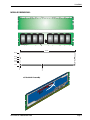
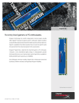
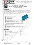
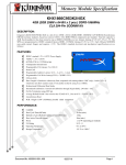
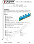
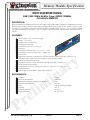
T E C H N O L O G Y
Memory Module Specification
KHX1333C9D3B1K2/2G
2GB (1GB 128M x 64-Bit x 2 pcs.) DDR3-1333MHz
CL9 240-Pin DIMM Kit
DESCRIPTION:
Kingston's KHX1333C9D3B1K2/2G is a kit of two 128M x 64-bit (1GB) DDR3-1333MHz CL9 SDRAM (Synchronous
DRAM) memory modules, based on eight 128M x 8-bit DDR3 FBGA components per module. Total kit capacity is 2GB.
The SPDs are programmed to JEDEC standard latency DDR3-1333MHz timing of 9-9-9 at 1.5V. Each 240-pin DIMM
uses gold contact fingers and requires +1.5V. The JEDEC standard electrical and mechanical specifications are as
follows:
FEATURES:
JEDEC standard 1.5V ± 0.075V Power Supply
VDDQ = 1.5V ± 0.075V
667MHz fCK for 1333Mb/sec/pin
8 independent internal bank
Programmable CAS Latency: 5,6,7,8,9,10
Posted CAS
Programmable Additive Latency: 0, CL - 2, or CL - 1 clock
Programmable CAS Write Latency(CWL) = 7(DDR3-1333)
8-bit pre-fetch
Burst Length: 8 (Interleave without any limit, sequential with starting address “000” only), 4 with tCCD = 4
which does not allow seamless read or write [either on the fly using A12 or MRS]
Bi-directional Differential Data Strobe
Internal(self) calibration : Internal self calibration through ZQ pin (RZQ : 240 ohm ± 1%)
On Die Termination using ODT pin
Average Refresh Period 7.8us at lower then TCASE 85°C, 3.9us at 85°C < TCASE . 95°C
Asynchronous Reset
PCB : Height 1.180” (30.00mm), single sided component
PERFORMANCE:
CL(IDD)
Row Cycle Time (tRCmin)
Refresh to Active/Refresh Command Time (tRFCmin)
Row Active Time (tRASmin)
Power
UL Rating
Operating Temperature
9 cycles
49.5ns (min.)
110ns
36ns (min.)
1.080 W (operating per module)
94 V - 0
0o C to 85o C
Storage Temperature
-55o C to +100o C
Document No. 4805634-001.A00
06/22/10
Page 1
ValueRAM
MODULE DIMENSIONS:
T E C H N O L O G Y
133.35
Units: millimeters
30.00
18.80
15.80
11.00
8.00
54.70
0.00
0.00
w/ Heatsink Assembly
Document No. 4805634-001.A00
Page 2