1
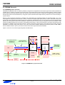
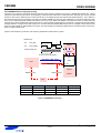
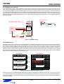
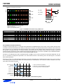
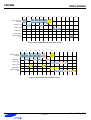
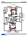
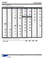
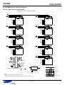
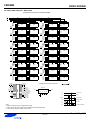
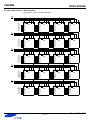
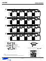
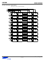
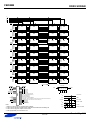
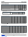
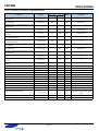
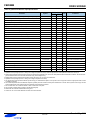
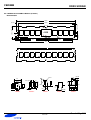
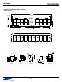
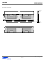
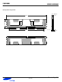
FBDIMM
DDR2 SDRAM
DDR2 Fully Buffered DIMM
240pin FBDIMMs based on 1Gb Q-die
60FBGA with Lead-Free and Halogen-Free
(RoHS compliant)
INFORMATION IN THIS DOCUMENT IS PROVIDED IN RELATION TO SAMSUNG PRODUCTS, AND IS SUBJECT TO CHANGE WITHOUT NOTICE. NOTHING IN THIS DOCUMENT SHALL BE CONSTRUED AS GRANTING ANY LICENSE, EXPRESS OR IMPLIED, BY ESTOPPEL OR OTHERWISE, TO ANY INTELLECTUAL
PROPERTY RIGHTS IN SAMSUNG PRODUCTS OR TECHNOLOGY. ALL INFORMATION IN THIS DOCUMENT
IS PROVIDED ON AS "AS IS" BASIS WITHOUT GUARANTEE OR WARRANTY OF ANY KIND.
1. For updates or additional information about Samsung products, contact your nearest Samsung office.
2. Samsung products are not intended for use in life support, critical care, medical, safety equipment, or similar applications where Product failure could result in loss of life or personal or physical harm, or any military or defense
application, or any governmental procurement to which special terms or provisions may apply.
* Samsung Electronics reserves the right to change products or specification without notice.
1 of 42
Rev. 1.4 May 2009
FBDIMM
DDR2 SDRAM
Table of Contents
1.0 FEATURES .....................................................................................................................................4
2.0 FBDIMM GENERALS .....................................................................................................................5
2.1 FB-DIMM Operation Overview ........................................................................................................5
.............................................................................................6
2.3 FB-DIMM Clocking Scheme ............................................................................................................7
2.4 FB-DIMM Protocol ........................................................................................................................7
2.5 Southbound Command Delivery .....................................................................................................8
2.6 Basic Timing Diagram ...................................................................................................................9
2.7 Advanced Memory Buffer Block Diagram ......................................................................................11
2.8 Interfaces ..................................................................................................................................12
3.0 FBD HIGH-SPEED DIFFERENTIAL POINT TO POINT LINK (at 1.5 V) INTERFACE ...............12
3.1 DDR2 Channel ............................................................................................................................12
3.2 SMBus Slave Interface ................................................................................................................12
2.2 FB-DIMM Channel Frequency Scaling
.................................................................................................................13
3.4 Peak Theoretical Throughput .......................................................................................................13
3.5 Hot-add .....................................................................................................................................13
3.6 Hot remove ................................................................................................................................13
3.7 Hot replace ................................................................................................................................13
4.0 PIN CONFIGUREATION ..............................................................................................................14
5.0 FBDIMM FUNCTIONAL BLOCK DIAGRAM ...............................................................................16
5.1 1GB, 128Mx72 Module - M395T2863QZ4 ........................................................................................16
5.2 2GB, 256Mx72 Module - M395T5663QZ4 ........................................................................................17
5.3 4GB, 512Mx72 Module - M395T5160QZ4 .......................................................................................18
5.4 4GB, 512Mx72 Module - M395T5163QZ4 .......................................................................................19
5.5 8GB, 1Gx72 Module - M395T1G60QJ4 .......................................................................................21
6.0 ELECTRICAL CHARACTERISTICS ............................................................................................23
7.0 CHANNEL INITIALIZATION ........................................................................................................32
3.3 FBD Channel Latency
2 of 42
Rev. 1.4 May 2009
FBDIMM
DDR2 SDRAM
Revision History
Revision
Month
Year
History
1.0
March
2008
- Initial Spec. Release
1.1
March
2008
- Added 4Rank Products based on Low Power AMB
1.11
March
2008
- Corrected Typo
1.12
April
2008
- Corrected mechanical Dimension
1.2
August
2008
- Changed the ordering information
1.3
December
2008
- Updated the IDD current specification
1.4
May
2009
- Added new products on the line-up (Based on Montage D3 AMB)
3 of 42
Rev. 1.4 May 2009
FBDIMM
DDR2 SDRAM
1.0 Features
-
- 240pin fully buffered dual in-line memory module (FBDIMM)
- 3.2Gb/s, 4.0Gb/s link transfer rate
- 1.8V +/- 0.1V Power Supply for DRAM VDD/VDDQ
- 1.5V +0.075/-0.045V Power Supply for AMB VCC
- 3.3V +/- 0.3V Power Supply for VDDSPD
- Buffer Interface with high-speed differential point-topoint Link at 1.5 volt
- Channel error detection & reporting
- Channel fail over mode support
Serial presence detect with EEPROM
8 Banks
Posted CAS
Programmable CAS Latency: 3, 4, 5, 6
Programmable Additive Latency: 0, 1, 2, 3, 4, 5
Automatic DDR2 DRAM bus and channel calibration
MBIST and IBIST Test functions
Hot add-on and Hot Remove Capability
Transparent mode for DRAM test support
[ Table 1 ] Ordering Information
Part Number
Density Organization
Component Composition
Number
of Rank
AMB
M395T2863QZ4-CE66/F76/E76
IDT C1
M395T2863QZ4-CE65
Intel D1
1GB
M395T2863QZ4-CE68/F78
128M x 72
128Mx8(K4T1G084QQ) *9EA
1
Type of
Heat
Spreader
Height
Full Module
30.35mm
IDT L4
M395T2863QZ4-CE63
Montage D3
M395T5663QZ4-CE66/F76/E76
IDT C1
M395T5663QZ4-CE65
Intel D1
2GB
M395T5663QZ4-CE68/F78
256M x 72
128Mx8(K4T1G084QQ) *18EA
2
IDT L4
M395T5663QZ4-CE63
Montage D3
M395T5160QZ4-CE66/F76/E76
IDT C1
M395T5160QZ4-CE65
Intel D1
M395T5160QZ4-CE68
4GB
512M x 72
256Mx4(K4T1G044QQ) *36EA
2
IDT L4
M395T5160QZ4-CE63
Montage D3
M395T5163QZ4-CE68/F78/E78
M395T1G60QJ4-CE68/F78
8GB
1G x 72
128Mx8(K4T1G084QQ) *36EA
4
IDT L4
DDP 512Mx4(K4T2G044QQ)
*36EA
4
IDT L4
Note :
1. “Z” of Part number(11th digit) stands for Lead-Free and RoHS compliant products.
2. “J” of Part number(11th digit) stands for Dual-Die Package based, Lead-Free and RoHS compliant products.
3. The last digit stands for AMB.
[ Table 2 ] Performance range
F7(DDR2-800)
DDR2 DRAM Speed
CL-tRCD-tRP
E7(DDR2-800)
E6(DDR2-667)
Unit
800
800
667
Mbps
6-6-6
5-5-5
5-5-5
CK
[ Table 3 ] Address Configuration
Organization
Row Address
Column Address
Bank Address
Auto Precharge
128Mx8(1Gb) based Module
A0-A13
A0-A9
BA0-BA2
A10
256Mx4(1Gb) based Module
A0-A13
A0-A9, A11
BA0-BA2
A10
4 of 42
Rev. 1.4 May 2009
FBDIMM
DDR2 SDRAM
2.0 FBDIMM Generals
2.1 FBDIMM Operation Overview
FB-DIMM (Fully Buffered Dual in Line Memory Module) is designed for the applications which require higher data transfer bandwidth and
scalable memory capacity. The memory slot access rate per channel decreases as the memory bus speed increases, resulting in limited
density build-up as channel speeds increase with memory system having the stub-bus architecture. FB-DIMM solution is intended to
eliminate this stub-bus channel bottleneck by using point-to-point links that enable multiple memory modules to be connected serially to
a given channel.
Memory system architecture perspective, FB-DIMM is fully differentiated from Registered DIMM and Unbuffered DIMM. A lot of new
technologies are integrated into this solution in order to achieve this scalable higher speed memory solution. Serial link interface with
packet data format and dedicated read/write paths are key attribute in FB-DIMM protocol. Point to Point interconnect with fully differential
signaling and de-emphasis scheme are key attribute in FBD channel link. Clock recovery by using data stream is key attribute in FBD
clocking. FB-DIMM supports both clock resync and resampling mode options. CRC (Cyclic Redundancy Check) bits are transferred with
data stream for reliability at high speed data transaction. Failover mechanism supports system running with dynamic IO failure. Finally all
FB-DIMM is connected in daisy chain manner. Thus, every interconnection between AMB (advanced memory buffer) to AMB, AMB to
Host and AMB to DRAM, is point to point interconnection which allows higher data transfer bandwidth.
Figure 1 shows a lot of new technologies integrated with FBD solution.
DRAM
Two unidirectional links
- Northbound
- Southbound
Protocol Packet
ADDR.CMD, DATA
SB (ADDR, CMD, Wdata)
Host
NB(Rdata)
P2P Interconnect
- LVDS
- De-Emphasis
DRAM
DQs ADDR CLK
CMD
Tx
Rx
Tx
Tx
Rx
AMB
Rx
ADDR
DQs CMD
Clk_Ref
DRAM
Reliability
Clock Recovery
- CRC fail-over
DRAM
AMB
Tx
Rx
Daisy Chain
Connection
Upto 8 AMB
CLK
DIMM Topology
Fly-by CLK, CMD
FIFO
Buffer
Clock
Figure 1. FBDIMM Memory system Overview
5 of 42
Rev. 1.4 May 2009
FBDIMM
DDR2 SDRAM
2.2 FBDIMM Channel Frequency Scaling
There are many frequency parameters including reference clock frequency, DRAM clock frequency, DRAM data transfer rate, channel
transfer rate and channel unit interval. All of frequency parameters are scaled with a certain gear ratio. External clock source provides
reference clock input to AMB and Host. External clock source is relatively slower than channel and DRAM frequency. Thus, AMB doubles external clock input and generates clock inputs to DRAMs. DRAM use clock input from AMB which is two times faster than reference clock for DRAM operation. DRAM data transfer rate is two times faster than DRAM clock input with nature of double data rate
operation and four times faster than external clock source. Channel speed is represented by unit interval - average time interval between
voltage transitions of a signal in the FBD channel. It is six times faster than DRAM data transfer rate. For example, external clock source
gives 6ns clock (166MHz), AMB doubles it and gives 3ns clock (333MHz) to DRAM and FBD channel communicate with unit interval 250ps (4.0Gbps transfer rate).
Figure 2 shows frequency scale ratio over frequency parameters in FBD memory system.
DDR667 Ex.
6ns
CLK_REF
3ns
CLK_DRAM
DRAM
250ps Packet T/F
DRAM
12 UIs in one CLK_DRAM
DQs ADDR CLK
CMD
Rx
Tx
SB (ADDR, CMD, Wdata)
Tx
Host
AMB
Rx
Clk_Ref
NB(Rdata)
DRAM
Reference CLK
Reference CLK
DRAM
Clock
UI
CLK_DRAM
CLK_REF
Frequency
312.5ps
266MHz
133MHz
3.2Gb/s
DDR2-667
250ps
333MHz
166MHz
4.0Gb/s
DDR2-800
208.33ps
400MHz
200MHz
4.8Gb/s
DDR2-533
Figure 2. FBDIMM Speed Scaling
6 of 42
Rev. 1.4 May 2009
FBDIMM
DDR2 SDRAM
2.3 FBDIMM Clocking Scheme
In FB-DIMM platform design, phase adjustment among reference clock inputs to each individual AMB and host is not taken account.
Thus, clock synchronization is made by using both external reference clock and channel data stream in FB-DIMM memory system. Host
and each individual AMB has a each individual IO basis clock recovery circuitry for channel data communication. It runs with inputs from
PLL inside chip and data stream from the other AMB or Host. Because data stream itself involves data communication process, no signaling switching or data communication may loss clock synchronization between transmitter and receiver. Thus, min transition density is
defined for this purpose. In FBD channel, a density of 6 transitions within 512 transfers or unit intervals (UI) on the channel is required for
interpolator training.
Using Reference CLK (Not in Phase)
Adjust edge/phase by; Min. Transition Density
Min. Transition Density
6 Transitions
DRAM
DRAM
SB (ADDR, CMD, Wdata)
Host
Tx
NB(Rdata)
512 Transfers
DQs ADDR CLK
CMD
Rx
Tx
AMB
Rx
Clk_Ref
DRAM
Clock
Recovery
Reference CLK
DRAM
Clock
Figure 3. FB-DIMM Clocking
2.4 FBDIMM Protocol
FB-DIMM channel has two unidirectional communication paths - south bound and north bound. South bound and north bound use physically different signal path. South and north mean direction of signal transaction. Southbound means direction of signals running from the
host controller toward the DIMMs. North is the opposite of south. Due to nature of memory operation, southbound carries information including command to DRAM, address to DRAM and write data to DRAM, while north bound carries read data from DRAM. In channel protocol point of view, southbound and northbound have different data frame formats and frame format size is optimized to ratio of read and
write. Data transfer perspective, read data transfer rate of north bound is twice faster than write data transfer. Higher channel utilization
achieves with asymmetric read and write data transfer rate.
Sout bound
Command (with Address)
Northbound
A CMD
Command (with Address)
or Write Data in
B CMD
Command (with Address)
or Write Data in
C CMD
R_Data(x72bits)
R_Data(x72bits)
Figure 4. Southbound / Northbound Frame format
Southbound consists of 10 differential signal pairs (lane), physically 20 signaling line. Southbound Format has 10x12 (10 IO (or Lane) x
12 IO switching) frame format, which deliver 10x12 bit information per one DRAM clock. One south bound frame is divided into three command slot. See Figure 5. Command slot A delivers command (with address). Command slot B and C delivers command (with address) or
write data into DRAM
7 of 42
Rev. 1.4 May 2009
FBDIMM
DDR2 SDRAM
Southbound Command Frame Format*
Bit
Transfer
0
1
2
3
4
5
6
7
8
9
10
11
9
aE0
aE1
aE2
aE3
FE21
FE20
FE19
FE18
FE17
FE16
FE15
FE14
8
aE7
aE6
aE5
aE4
0
0
0
0
0
0
0
0
7
6
5
4
3
2
aE8 F0=0 aC20 aC16 aC12 aC8
aE9 F1=0 aC21 aC17 aC13 aC9
aE10 aE13 aC22 aC18 aC14 aC10
aE11 aE12 aC23 aC19 aC15 aC11
0
0 bC20 bC16 bC12 bC8
0
0 bC21 bC17 bC13 bC9
0
0 bC22 bC18 bC14 bC10
0
0 bC23 bC19 bC15 bC11
0
0 cC20 cC16 cC12 cC8
0
0 cC21 cC17 cC13 cC9
0
0 cC22 cC18 cC14 cC10
0
0 cC23 cC19 cC15 cC11
FE0
FE1
FE2
FE3
FE7
FE6
FE5
FE4
FE11
FE10
FE9 FE13
FE8 FE12
1
aC4
aC5
aC6
aC7
bC4
bC5
bC6
bC7
cC4
cC5
cC6
cC7
0
aC0
aC1
aC2
aC3
bC0
bC1
bC2
bC3
cC0
cC1
cC2
cC3
CLK_REF
A CMD
CLK_DRAM
Packet T/F
B CMD
x10 bits
C CMD
12 transfers
Note :
1. aE[0~12] : CRC Checksum of the A Command
2. F[0~1] : Frame Type
3. FE[0~21] : CRC Checksum of 72bit data
4. CRC : Cyclic Redundancy Check
Figure 5. FBDIMM Command Encoding & SB Frame
DRAM Cmnds
Activate
Write
Read
Precharge All
Precharge Single
Auto (CBR) Refresh
Enter Self Refresh
Exit Self Refresh/
Exit Power Down
Enter Power Down
reserved
23
DS2
DS2
DS2
DS2
DS2
DS2
DS2
22
DS1
DS1
DS1
DS1
DS1
DS1
DS1
21
DS0
DS0
DS0
DS0
DS0
DS0
DS0
20
1
0
0
0
0
0
0
19
18
DRAM Addr
1
1
1
0
0
1
0
1
0
1
0
1
17
RS
RS
RS
RS
RS
RS
RS
16
X
X
X
15
14
X
X
DRAM Bank
X
X
X
X
13
12
11
10
X
X
X
1
1
1
1
1
1
0
0
1
0
1
0
9
8
7
DRAM Bank & Address
DRAM Bank & Address
DRAM Bank & Address
X
X
X
X
X
X
X
X
X
X
X
X
6
5
4
3
2
1
0
X
X
X
X
X
X
X
X
X
X
X
X
X
X
X
X
X
X
X
X
X
X
X
X
X
X
X
X
X
DS2
DS1
DS0
0
0
1
RS
X
X
X
X
0
1
1
X
X
X
X
X
X
X
X
X
DS2
DS1
DS0
0
0
1
RS
X
X
X
X
0
1
0
X
X
X
X
X
X
X
X
X
X
X
X
X
0
0
1
X
X
X
X
X
0
0
X
X
X
X
X
X
X
X
X
X
X
Note : The values in “ X” fields in non-reserved commands above may be driven onto the DRAM device pins.
2.5 Southbound Command Delivery
A DRAM command located in the "A" command may be delivered to the DRAM devices as soon as the 14-bit (10-bits in fail-over) CRC
is checked. This minimizes DRAM access latency by allowing the command to be delivered after the first 4 transfers of the frame have
been received. The "A" command is transferred immediately to the DRAM pins with minimum delay whereas the "B" and "C" command
are delivered one DRAM clock later. To minimize memory access latency the read related Activate, Read (if the page is open) and
explicit Precharge commands to a rank of DRAM devices should be placed in the "A" command, if possible. Figure 6 illustrates the delivery of the three potential commands in a frame to three separate DRAM channels.
Command "A" is delivered in this case to the DRAM devices on DIMM 3 as soon as the command can traverse the AMB buffer. The "B"
and "C" commands are delayed and presented to two other DRAM channels on the following clock. See below figure7~10 for Basic
Read & Write Operations
Northbound consists of 14 differential signal pairs (lane), physically 28 signaling line. Southbound Format has 14x12 (14 IO (or Lane) x
12 IO switching) frame format, which deliver 14x12 bit information per one DRAM clock. One north bound frame is divided into two. Both
frame deliver read data from DRAM
1
FBD southbound
cmd/data
DIMM 1 cmd
2
“A”
“B”
“C”
DIMM 4 cmd
4
5
1. CMD A transferred immediately
2. CMD A, B, C cannot target the same DIMM
3. Host is responsible for scheduling CMD
DIMM 2 cmd
DIMM 3 cmd
3
“C”
“A”
“B”
FBD northbound
cmd/data
Figure 6. FBDIMM Command Delivery Rules
8 of 42
Rev. 1.4 May 2009
FBDIMM
DDR2 SDRAM
2.6 Basic Timing Diagram
1
FBD southbound
cmd/data
2
3
4
ACT1
NOP
NOP
5
6
7
8
9
10
11
12
13
RD1
NOP
NOP
DIMM 1 cmd
ACT1
RD1
DIMM 1 data
DIMM 2 cmd
DIMM 2 data
FBD northbound
data
Figure 7. Basic DRAM Read Data Transfers on FBD
1
FBD southbound
cmd/data
DIMM 1 cmd
2
ACT1
NOP
NOP
3
4
ACT2
NOP
NOP
RD1
NOP
NOP
ACT1
5
6
7
8
9
10
11
12
13
RD2
NOP
NOP
RD1
DIMM 1 data
DIMM 2 cmd
ACT2
RD2
DIMM 2 data
FBD northbound
data
No Bubble
Figure 8. Back to Back DRAM Read Data Transfers
9 of 42
Rev. 1.4 May 2009
FBDIMM
DDR2 SDRAM
1
FBD southbound
cmd/data
2
3
ACT1
NOP
NOP
DIMM 1 cmd
4
5
6
7
8
9
10
11
12
13
NOP WR1 NOP NOP SYNC
Wdata Wdata Wdata Wdata 1010
Wdata Wdata Wdata Wdata 0101
ACT1
WR1
Fixed fall through time
DIMM 1 data
DIMM 2 cmd
DIMM 2 data
FBD northbound
data
Status
Figure 9. Basic DRAM Write Data Transfers on FBD
1
2
3
4
5
FBD southbound ACT1 ACT2 ACT3 RD1 WR2
cmd/data Wdata Wdata Wdata Wdata NOP
Wdata Wdata Wdata Wdata NOP
DIMM 1 cmd
ACT1
ACT3
6
7
RD3
NOP
NOP
RD1
8
9
10
11
12
13
SYNC
1010
0101
RD3
DIMM 1 data
DIMM 2 cmd
ACT2
WR2
DIMM 2 data
FBD northbound
data
Status
Figure 10. Simultaneous RD / WR Data Transfers
10 of 42
Rev. 1.4 May 2009
FBDIMM
DDR2 SDRAM
2.7 Advanced Memory Buffer Block Diagram
Advance Memory Buffer
Block Diagram
10x2
Southbound
Data In
NORTH
10x2
Southbound
Data Out
Data Merge
Re-Time
1x2
Re-synch
PLL
demux
Ref Clock
PISO
10*2
Reset#
10*2
mux
Link Init SM
and Control
and CSRs
Reset
Control
lnit
patterns
4
DRAM Clock
IBIST - RX
Command
Decoder &
CRC Check
IBIST - TX
4
DRAM Clock #
failover
LAI Logic
29
Cmd Out
mux
Thermal
Sensor
DDR
IOs
DRAM Cmd
DDR State
Controller
and CSRs
mux
36
deep
Write
Data
FIFO
72 + 18x2
External MEMBIST
DDR calibration &
DDR IOBIST/DFX
Data CRC Gen
& Read FIFO
Sync & ldie
Pattern
Generator
IBIST -TX
DRAM
Data / strobe
Data In
LAI
Controller
SMbus
Controller
DRAM Address /
Command Copy 2
Data Out
Core Control
and CSRs
SMbus
29
DRAM Address /
Command Copy 1
NB LAI Buffer
IBIST - RX
mux
Link lnit SM
and Control
and CSRs
failover
14*6*2
14*12
PISO
demux
Re-synch
Re-Time
Data Merge
Northbound
Data Out
14x2
14x2
Northbound
Data In
Figure 11. Advanced Memory Buffer Block Diagram
11 of 42
Rev. 1.4 May 2009
FBDIMM
DDR2 SDRAM
2.8 Interfaces
Figure 12 illustrates the Advanced Memory Buffer and all of its interfaces. They consist of two FBD links, one DDR2 channel and an SMBus interface. Each FBD link connects the Advanced Memory Buffer to a host memory controller or an adjacent FBD. The DDR2 channel
supports direct connection to the DDR2 SDRAMs on a Fully Buffered DIMM
Primary or
Host Direction
NB FBD
Out Link
AMB
NB FBD
In Link
SB FBD
Out Link
SB FBD
In Link
SMB
Secondary or
to optional next FBD
DDR2
CHANNEL
MEMORY INTERFACE
Figure 12. Advanced Memory Buffer Interface Block Diagram
The FBDIMM channel uses a daisy-chain topology to provide expansion from a single DIMM per channel to up to 8 DIMMs per channel.
The host sends data on the southbound link to the first DIMM where it is received and redriven to the second DIMM. On the southbound
data path each DIMM receives the data and again redrives the data to the next DIMM until the last DIMM receives the data. The last DIMM
in the chain initiates the transmission of data in the direction of the host (a.k.a. northbound). On the northbound data path each DIMM
receives the data and re-drives the data to the next DIMM until the host is reached.
3.0 FBD HIGH-SPEED DIFFERENTIAL POINT TO POINT LINK (at 1.5 V) INTERFACE
The Advanced Memory Buffer supports one FBD Channel consisting of two bidirectional link interfaces using high-speed differential pointto-point electrical signaling.
The southbound input link is 10 lanes wide and carries commands and write data from the host memory controller or the adjacent DIMM
in the host direction. The southbound output link forwards this same data to the next FBD.
The northbound input link is 14 lanes wide and carries read return data or status information from the next FBDIMM in the chain back
towards the host. The northbound output link forwards this information back towards the host and multiplexes in any read return data or
status information that is generated internally.
3.1 DDR2 Channel
The DDR2 channel on the Advanced Memory Buffer supports direct connection to DDR2 SDRAMs. The DDR2 channel supports two
ranks of eight banks with 16 row/column request, 64 data signals, and eight check-bit signals. There are two copies of address and command signals to support DIMM routing and electrical requirements. Four-transfer bursts are driven on the data and check-bit lines at 800
MHz.
Propagation delays between read data/check-bit strobe lanes on a given channel can differ. Each strobe can be calibrated by hardware
state machines using write/read trial and error (or equivalent implementation). Hardware aligns the read data and check-bits to a single
core clock.
The Advanced Memory Buffer provides four copies of the command clock phase references (CLK[3:0]) and write data/check-bit .
3.2 SMBus Slave Interface
The Advanced Memory Buffer supports an SMBus interface to allow system access to configuration registers independent of the FBD
link. The Advanced Memory Buffer will never be a master on the SMBus, only a slave. Serial SMBus data transfer is supported at 100
kHz. SMBus access to the Advanced Memory Buffer may be a requirement to boot a system. This provides a mechanism to set link
strength, frequency and other parameters needed to insure robust operation given platform specific configurations. It is also required for
diagnostic support when the link is down. The SMBus address straps located on the DIMM connector are used by the Advanced Memory
Buffer to get its unique ID.
12 of 42
Rev. 1.4 May 2009
FBDIMM
DDR2 SDRAM
3.3 FBD Channel Latency
FBD channel latency is measured from the time a read request is driven on the FBD channel pins to the time when the first 16 bytes (2nd
chunk) of read completion data is sampled by the memory controller.
When not using the Variable Read Latency capability, the latency for a specific FBDIMM on an FBD channel is always equal to the latency
for any other FBDIMM on that channel. However, the latency for each FBDIMM in a specific configuration with some number of FBDIMMs
installed may not be equal to the latency for each FBDIMM in a configuration with some different number of FBDIMMs installed.
As more DIMMs are added to the FBD channel, additional latency is required to read from each DIMM on the channel. Because the FBD
channel is based on the point-to-point interconnection of buffer components between DIMMs, memory requests are required to travel
through N-1 buffers before reaching the Nth buffer. The result is that a four DIMM channel configuration will have greater idle read latency
compared to a one DIMM channel configuration.
The Variable Read Latency capability can be used to reduce latency for DIMMs closer to the host.
The idle latencies listed in this section are representative of what might be achieved in typical AMB designs. Actual implementations with
latencies less than the values listed will have higher application performance and vice versa.
3.4 Peak Theoretical Throughput
An FBD channel transfers read completion data on the FBD Northbound data connection. 144 bits of data are transferred for every FBD
Northbound data frame. This matches the 18-byte data transfer of an ECC DDR DRAM in a single DRAM command clock. A DRAM burst
of 8 from a single channel or a DRAM burst of four from two lock-stepped channels provides a total of 72 bytes of data (64 bytes plus 8
bytes ECC).
The FBD frame rate matches the DRAM command clock because of the fixed 6:1 ratio of the FBD channel clock to the DRAM command
clock. Therefore, the Northbound data connection will exhibit the same peak theoretical throughput as a single DRAM channel. For example, when using DDR2 533 DRAMs, the peak theoretical bandwidth of the Northbound data connection is 4.267 GB/sec.
Write data is transferred on the FBD Southbound command and data connection, via Command+Wdata frames. 72 bits of data are transferred for every FBD Command+Wdata frame. Two Command+Wdata frames match the 18-byte data transfer of an ECC DDR DRAM in
a single DRAM command clock. A DRAM burst of 8 transfers from a single channel, or a burst of 4 from two lock-step channels provides
a total of 72 bytes of data (64 bytes plus 8 bytes ECC).
When the FBD frame rate matches the DRAM command clock, the Southbound command and data connection will exhibit one half the
peak theoretical throughput of a single DRAM channel. For example, when using DDR2 533 DRAMs, the peak theoretical bandwidth of
the Southbound command and data connection is 2.133 GB/sec.
The total peak theoretical throughput for a single FBD channel is defined as the sum of the peak theoretical throughput of the Northbound
data connection and the Southbound command and data connection. When the FBD frame rate matches the DRAM command clock, this
is equal to 1.5 times the peak theoretical throughput of a single DRAM channel. For example, when using DDR2 533 DRAMs, the peak
theoretical throughput of a DDR2 533 channel would be 4.267 GB/sec, while the peak theoretical throughput of an FBD-533 channel would
be 6.4 GB/sec.
3.5 Hot-add
The FBDIMM channel does not provide a mechanism to automatically detect and report the addition of a new FBDIMM south of the currently active last FBDIMM. It is assumed the system will be notified through some means of the addition of one or more new FBDIMMs
so that specific commands can be sent to the host controller to initialize the newly added FBDIMM(s) and perform a hot-add reset to bring
them into the channel timing domain. It should be noted that the power to the FBDIMM socket must be removed before a hot-add FBDIMM
is inserted or removed. Applying or removing the power to a FBDIMM socket is a system platform function.
3.6 Hot remove
In order to accomplish removal of FBDIMMs, the host must perform a fast reset sequence targeted at the last FBDIMM that will be retained
on the channel. The fast reset re-establishes the appropriate last FBDIMM so that the southbound transmission outputs of the last active
FBDIMM and the southbound and northbound outputs of the FBDIMMs beyond the last active FBDIMM are disabled. Once the appropriate
outputs are disabled, the system can coordinate the procedure to remove power in preparation for physical removal of the FBDIMM if
needed. Note that the power to the FBDIMM socket must be removed before a hot-add FBDIMM is inserted or removed. Applying or removing the power to a FBDIMM socket is a system platform function.
3.7 Hot replace
Hot replace of FBDIMM is accomplished through combining the hot-remove and hotadd processes
13 of 42
Rev. 1.4 May 2009
FBDIMM
DDR2 SDRAM
4.0 Pin Configuration
[ Table 4 ] DDR2 240 Pin FBDIMM Configurations (Front side/Back side)
Pin
Front
Pin
Back
Pin
Front
Pin
Back
Pin
Front
Pin
Back
Pin
Front
Pin
Back
1
VDD
121
VDD
31
PN3
151
SN3
61
PN9
181
SN9
91
PS9
211
SS9
2
VDD
122
VDD
32
PN3
152
SN3
62
VSS
182
VSS
92
VSS
212
VSS
3
VDD
123
VDD
33
VSS
153
VSS
63
PN10
183
SN10
93
PS5
213
SS5
4
VSS
124
VSS
34
PN4
154
SN4
64
PN10
184
SN10
94
PS5
214
SS5
5
VDD
125
VDD
35
PN4
155
SN4
65
VSS
185
VSS
95
VSS
215
VSS
6
VDD
126
VDD
36
VSS
156
VSS
66
PN11
186
SN11
96
PS6
216
SS6
7
VDD
127
VDD
37
PN5
157
SN5
67
PN11
187
SN11
97
PS6
217
SS6
8
VSS
128
VSS
38
PN5
158
SN5
68
VSS
188
VSS
98
VSS
218
VSS
9
VCC
129
VCC
39
VSS
159
VSS
99
PS7
219
SS7
10
VCC
130
VCC
40
PN13
160
SN13
69
VSS
189
VSS
100
PS7
220
SS7
11
VSS
131
VSS
41
PN13
161
SN13
70
PS0
190
SS0
101
VSS
221
VSS
KEY
12
VCC
132
VCC
42
VSS
162
VSS
71
PS0
191
SS0
102
PS8
222
SS8
13
VCC
133
VCC
43
VSS
163
VSS
72
VSS
192
VSS
103
PS8
223
SS8
14
VSS
134
VSS
224
VSS
44
RFU*
164
RFU*
73
PS1
193
SS1
104
VSS
15
VTT
135
VTT
45
RFU*
165
RFU*
74
PS1
194
SS1
105
RFU**
225
RFU**
16
VID1
136
VID0
46
VSS
166
VSS
75
VSS
195
VSS
106
RFU**
226
RFU**
17
RESET
137
DNU/M_Test
47
VSS
167
VSS
76
PS2
196
SS2
107
VSS
227
VSS
18
VSS
138
VSS
48
PN12
168
SN12
77
PS2
197
SS2
108
VDD
228
SCK
19
RFU**
139
RFU**
49
PN12
169
SN12
78
VSS
198
VSS
109
VDD
229
SCK
20
RFU**
140
RFU**
50
VSS
170
VSS
79
PS3
199
SS3
110
VSS
230
VSS
21
VSS
141
VSS
51
PN6
171
SN6
80
PS3
200
SS3
111
VDD
231
VDD
22
PN0
142
SN0
52
PN6
172
SN6
81
VSS
201
VSS
112
VDD
232
VDD
23
PN0
143
SN0
53
VSS
173
VSS
82
PS4
202
SS4
113
VDD
233
VDD
24
VSS
144
VSS
54
PN7
174
SN7
83
PS4
203
SS4
114
VSS
234
VSS
25
PN1
145
SN1
55
PN7
175
SN7
84
VSS
204
VSS
115
VDD
235
VDD
26
PN1
146
SN1
56
VSS
176
VSS
85
VSS
205
VSS
116
VDD
236
VDD
27
VSS
147
VSS
57
PN8
177
SN8
86
RFU*
206
RFU*
117
VTT
237
VTT
28
PN2
148
SN2
58
PN8
178
SN8
87
RFU*
207
RFU*
118
SA2
238
VDDSPD
29
PN2
149
SN2
59
VSS
179
VSS
88
VSS
208
VSS
119
SDA
239
SA0
30
VSS
150
VSS
60
PN9
180
SN9
89
VSS
209
VSS
120
SCL
240
SA1
90
PS9
210
SS9
RFU = Reserved Future Use.
* These pin positions are reserved for forwarded clocks to be used in future module implementations
** These pin positions are reserved for future architecture flexibility
1. The following signals are CRC bits and thus appear out of the normal sequence : PN12/PN12, SN12/SN12, PN13/PN13, SN13/SN12,
PS9/PS9, SS9/SS9.
14 of 42
Rev. 1.4 May 2009
FBDIMM
DDR2 SDRAM
[ Table 5 ] Pin Description
Pin Name
Type
Pin Description
Pin Numbers
SCK
Input
System Clock Input, positive line
228
SCK
Input
System Clock Input, negative line
229
PN[13:0]
Output
Primary northbound Data, positive lines
22, 25, 28, 31, 34, 37, 40, 48, 51, 54, 57, 60, 63, 66
PN[13:0]
Output
Primary northbound Data, negative lines
23, 26, 29, 32, 35, 38, 41, 49, 52, 55, 58, 61, 64, 67
PS[9:0]
Input
Primary Southbound Data, positive lines
70, 73, 76, 79, 82, 90, 93, 96, 99, 102
PS[9:0]
Input
Primary Southbound Data, negative lines
71, 74, 77, 80, 83, 91, 94, 97, 100, 103
SN[13:0]
Output
Secondary Northbound Data, positive lines
142, 145, 148, 151, 154, 157, 160, 168, 171, 174, 177,
180, 183, 186
SN[13:0]
Output
Secondary Northbound Data, negative lines
143, 146, 149, 152, 155, 158, 161, 16, 172, 175, 178,
181, 184, 187
SS[9:0]
Input
Secondary Southbound Data, positive lines
190, 193, 196, 199, 202, 210, 213, 216, 219, 222
SS[9:0]
Input
Secondary Southbound Data, negative lines
191, 194, 197, 200, 203, 211, 214, 217, 220, 223
SCL
Input
Serial Presence Detect (SPD) Clock Input
120
SDA
Input
SPD Data Input / Output
119
SA[2:0]
Input
SPD Address Inputs, also used to select the DIMM number in
118, 239, 240
the AMB
Voltage ID : These pins must be unconnected for DDR2 based Fully Buffered DIMMs
16, 136
VID[0] is VDD value : OPEN = 1.8 V, GND = 1.5 V ; VID[1] is VCC
value : OPEN = 1.5V, GND = 1.2V
VID[1:0]
NC
RESET
Input
AMB reset signal
17
RFU
RFU
Reserved for Future Use
19, 20, 44, 45, 86, 87, 105, 106, 139, 140, 164, 165,
206, 207, 225, 226
VCC
PWR
AMB Core Power and AMB Channel Interface Power (1.5 Volt) 9, 10, 12, 13, 129, 130, 132, 133
VDD
PWR
DRAM Power and AMB DRAM I/O Power (1.8Volt)
VTT
PWR
DRAM Address/Command/Clock Termination Power(VDD/2)
15, 117, 135, 237
VDDSPD
PWR
SPD Power
238
GND
Ground
4, 8, 11, 14, 18, 21, 24, 27, 30, 33, 36, 39, 42, 43, 46,
47, 50, 53, 56, 59, 62, 65, 68, 69, 72, 75, 78, 81, 84, 85,
88, 89, 92, 95, 98, 101, 104, 107, 110, 114, 124, 128,
131, 134, 138, 141, 144, 147, 150, 153, 156, 159, 162,
163, 166, 167, 170, 173, 176, 179, 182, 185, 188, 189,
192, 195, 198, 201, 204, 205, 208, 209, 212, 215, 218,
221, 224, 227, 230, 234
DNU
The DNU/M_Test pin provides an external connection R/Cs AD for testing the margin of Vref which is produced by a voltage
divider on the module. It is not intended to be used in normal
system operation and must not be connected (DNU) in a sys- 137
tem. This test pin may have other features on future card designs and if it does, will be included in this specification at that
time.
VSS
DNU/M_Test
15 of 42
1, 2, 3, 5, 6, 7, 108, 109, 111, 112, 113, 115, 116, 121,
122, 123, 125, 126, 127, 231, 232, 233, 235, 236
Rev. 1.4 May 2009
FBDIMM
DDR2 SDRAM
5.0 FBDIMM Functional Block Diagram
5.1 1GB, 128Mx72 Module - M395T2863QZ4
(populated as 1 rank of x8 DDR2 SDRAMs)
S0
DQS0
DQS0
DQS9
DQS4
DQS4
DQS13
DQ0
DQ1
DQ2
DQ3
DQ4
DQ5
DQ6
DQ7
DM/ NU/ CS
RDQS RDQS
I/O 0
I/O 1
I/O 2
I/O 3
I/O 4
I/O 5
I/O 6
I/O 7
DQS DQS
DQ32
DQ33
DQ34
DQ35
DQ36
DQ37
DQ38
DQ39
D0
DQS1
DQS1
DQS10
DM/ NU/ CS
RDQS RDQS
I/O 0
I/O 1
I/O 2
I/O 3
I/O 4
I/O 5
I/O 6
I/O 7
DQS DQS
D4
DQS5
DQS5
DQS14
DQ8
DQ9
DQ10
DQ11
DQ12
DQ13
DQ14
DQ15
DM/ NU/ CS
RDQS RDQS
I/O 0
I/O 1
I/O 2
I/O 3
I/O 4
I/O 5
I/O 6
I/O 7
DQS DQS
DQ40
DQ41
DQ42
DQ43
DQ44
DQ45
DQ46
DQ47
D1
DQS2
DQS2
DQS11
DM/ NU/ CS
RDQS RDQS
I/O 0
I/O 1
I/O 2
I/O 3
I/O 4
I/O 5
I/O 6
I/O 7
DQS DQS
D5
DQS6
DQS6
DQS15
DQ16
DQ17
DQ18
DQ19
DQ20
DQ21
DQ22
DQ23
DM/ NU/ CS
RDQS RDQS
I/O 0
I/O 1
I/O 2
I/O 3
I/O 4
I/O 5
I/O 6
I/O 7
DQS DQS
DQ48
DQ49
DQ50
DQ51
DQ52
DQ53
DQ54
DQ55
D2
DM/ NU/ CS
RDQS RDQS
I/O 0
I/O 1
I/O 2
I/O 3
I/O 4
I/O 5
I/O 6
I/O 7
DQS DQS
D6
DQS7
DQS7
DQS16
DQS3
DQS3
DQS12
DQ24
DQ25
DQ26
DQ27
DQ28
DQ29
DQ30
DQ31
DM/ NU/ CS
RDQS RDQS
I/O 0
I/O 1
I/O 2
I/O 3
I/O 4
I/O 5
I/O 6
I/O 7
PN0-PN13
PN0-PN13
PS0-PS9
PS0-PS9
DQ0-DQ63
CB0-CB7
DQS0-DQS17
DQS0-DQS8
SCL
SDA
SA1-SA2
SA0
RESET
SCK/SCK
DQS DQS
DQ56
DQ57
DQ58
DQ59
DQ60
DQ61
DQ62
DQ63
D3
CB0
CB1
CB2
CB3
CB4
CB5
CB6
CB7
S0->CS(all SDRAMs)
CKE0->CKE(all SDRAMs)
ODT->ODT(all SDRAMs)
BA0-BA2(all SDRAMs)
A0-A15(all SDRAMs)
RAS(all SDRAMs)
CAS(all SDRAMs)
WE(all SDRAMs)
CK/CK(all SDRAMs)
All address/command/control/clock
I/O 0
I/O 1
I/O 2
I/O 3
I/O 4
I/O 5
I/O 6
I/O 7
DQS DQS
D7
DQS8
DQS8
DQS17
SN0-SN13
SN0-SN13
SS0-SS9
SS0-SS9
A
M
B
DM/ NU/ CS
RDQS RDQS
DM/ NU/ CS
RDQS RDQS
I/O 0
I/O 1
I/O 2
I/O 3
I/O 4
I/O 5
I/O 6
I/O 7
DQS DQS
D8
Serial PD
SCL
VTT
SDA
WP A0
A1
A2
SA0 SA1 SA2
VTT
Terminators
VCC
AMB
VDDSPD
VDD
Note :
1.DQ-to I/O wiring may be changed within a byte.
2.There are two physical copies of each address/command/control/clock
16 of 42
VREF
VSS
SPD, AMB
D0-D8, AMB
D0-D8
D0-D8,SPD,AMB
Rev. 1.4 May 2009
FBDIMM
DDR2 SDRAM
5.2 2GB, 256Mx72 Module - M395T5663QZ4
(populated as 2 ranks of x8 DDR2 SDRAMs)
S1
S0
DQS0
DQS0
DQS9
DQS4
DQS4
DQS13
DQ0
DQ1
DQ2
DQ3
DQ4
DQ5
DQ6
DQ7
DM/ NU/ CS
RDQS RDQS
I/O 0
I/O 1
I/O 2
I/O 3
I/O 4
I/O 5
I/O 6
I/O 7
DQS DQS
DM/ NU/ CS
RDQS RDQS
I/O 0
I/O 1
I/O 2
I/O 3
I/O 4
I/O 5
I/O 6
I/O 7
D0
DQS DQS
DQ32
DQ33
DQ34
DQ35
DQ36
DQ37
DQ38
DQ39
D9
DQS1
DQS1
DQS10
DM/ NU/ CS
RDQS RDQS
I/O 0
I/O 1
I/O 2
I/O 3
I/O 4
I/O 5
I/O 6
I/O 7
DQS DQS
DM/ NU/ CS
RDQS RDQS
I/O 0
I/O 1
I/O 2
I/O 3
I/O 4
I/O 5
I/O 6
I/O 7
D4
DQS DQS
D13
DQS5
DQS5
DQS14
DQ8
DQ9
DQ10
DQ11
DQ12
DQ13
DQ14
DQ15
DM/ NU/ CS
RDQS RDQS
I/O 0
I/O 1
I/O 2
I/O 3
I/O 4
I/O 5
I/O 6
I/O 7
DQS DQS
DM/ NU/ CS
RDQS RDQS
I/O 0
I/O 1
I/O 2
I/O 3
I/O 4
I/O 5
I/O 6
I/O 7
D1
DQS DQS
DQ40
DQ41
DQ42
DQ43
DQ44
DQ45
DQ46
DQ47
D10
DQS2
DQS2
DQS11
DM/ NU/ CS
RDQS RDQS
I/O 0
I/O 1
I/O 2
I/O 3
I/O 4
I/O 5
I/O 6
I/O 7
DQS DQS
DM/ NU/ CS
RDQS RDQS
I/O 0
I/O 1
I/O 2
I/O 3
I/O 4
I/O 5
I/O 6
I/O 7
D5
DQS DQS
D14
DQS6
DQS6
DQS15
DQ16
DQ17
DQ18
DQ19
DQ20
DQ21
DQ22
DQ23
DM/ NU/ CS
RDQS RDQS
I/O 0
I/O 1
I/O 2
I/O 3
I/O 4
I/O 5
I/O 6
I/O 7
DQS DQS
DM/ NU/ CS
RDQS RDQS
I/O 0
I/O 1
I/O 2
I/O 3
I/O 4
I/O 5
I/O 6
I/O 7
D2
DQS DQS
DQ48
DQ49
DQ50
DQ51
DQ52
DQ53
DQ54
DQ55
D11
DM/ NU/ CS
RDQS RDQS
I/O 0
I/O 1
I/O 2
I/O 3
I/O 4
I/O 5
I/O 6
I/O 7
DQS DQS
DM/ NU/ CS
RDQS RDQS
I/O 0
I/O 1
I/O 2
I/O 3
I/O 4
I/O 5
I/O 6
I/O 7
D6
DQS DQS
D15
DQS7
DQS7
DQS16
DQS3
DQS3
DQS12
DQ24
DQ25
DQ26
DQ27
DQ28
DQ29
DQ30
DQ31
DM/ NU/ CS
RDQS RDQS
I/O 0
I/O 1
I/O 2
I/O 3
I/O 4
I/O 5
I/O 6
I/O 7
SCL
SDA
SA1-SA2
SA0
RESET
DM/ NU/ CS
RDQS RDQS
I/O 0
I/O 1
I/O 2
I/O 3
I/O 4
I/O 5
I/O 6
I/O 7
D3
DQS DQS
DQ56
DQ57
DQ58
DQ59
DQ60
DQ61
DQ62
DQ63
D12
S0->CS(D0-D8)
CKE0->CKE(D0-D8)
S1->CS(D9-D17)
CKE1->CKE(D9-D17)
A
M
B
CB0
CB1
CB2
CB3
CB4
CB5
CB6
CB7
ODT->ODT(all SDRAMs)
BA0-BA2(all SDRAMs)
A0-A15(all SDRAMs)
RAS(all SDRAMs)
CAS(all SDRAMs)
WE(all SDRAMs)
CK/CK(all SDRAMs)
SCK/SCK
All address/command/control/clock
Serial PD
SCL
SDA
WP A0
A1
DM/ NU/ CS
RDQS RDQS
I/O 0
I/O 1
I/O 2
I/O 3
I/O 4
I/O 5
I/O 6
I/O 7
DQS DQS
DM/ NU/ CS
RDQS RDQS
I/O 0
I/O 1
I/O 2
I/O 3
I/O 4
I/O 5
I/O 6
I/O 7
D7
DQS DQS
D16
DQS8
DQS8
DQS17
SN0-SN13
SN0-SN13
SS0-SS9
SS0-SS9
PN0-PN13
PN0-PN13
PS0-PS9
PS0-PS9
DQ0-DQ63
CB0-CB7
DQS0-DQS17
DQS0-DQS8
DQS DQS
A2
DM/ NU/ CS
RDQS RDQS
I/O 0
I/O 1
I/O 2
I/O 3
I/O 4
I/O 5
I/O 6
I/O 7
D8
Terminators
VCC
AMB
VREF
17 of 42
DQS DQS
VTT
VDD
Note :
1.DQ-to I/O wiring may be changed within a byte.
2.There are two physical copies of each address/command/control/clock
I/O 0
I/O 1
I/O 2
I/O 3
I/O 4
I/O 5
I/O 6
I/O 7
DQS DQS
D17
VTT
VDDSPD
SA0 SA1 SA2
DM/ NU/ CS
RDQS RDQS
VSS
SPD, AMB
D0-D17, AMB
D0-D17
D0-D17,SPD,AMB
Rev. 1.4 May 2009
FBDIMM
DDR2 SDRAM
5.3 4GB, 512Mx72 Module - M395T5160
(populated as 2 ranks of x4 DDR2 SDRAMs)
VSS
S1
S0
DQS0
DQS0
DQS9
DQS9
DM
DQ0
DQ1
DQ2
DQ3
DQS1
DQS1
I/O 0
I/O 1
I/O 2
I/O 3
DM
DQ8
DQ9
DQ10
DQ11
DQS2
DQS2
I/O 0
I/O 1
I/O 2
I/O 3
DM
DQ16
DQ17
DQ18
DQ19
DQS3
DQS3
I/O 0
I/O 1
I/O 2
I/O 3
DM
DQ24
DQ25
DQ26
DQ27
DQS4
DQS4
I/O 0
I/O 1
I/O 2
I/O 3
DM
DQ32
DQ33
DQ34
DQ35
DQS5
DQS5
I/O 0
I/O 1
I/O 2
I/O 3
DM
DQ40
DQ41
DQ42
DQ43
DQS6
DQS6
I/O 0
I/O 1
I/O 2
I/O 3
DM
DQ48
DQ49
DQ50
DQ51
DQS7
DQS7
I/O 0
I/O 1
I/O 2
I/O 3
DM
DQ56
DQ57
DQ58
DQ59
DQS8
DQS8
I/O 0
I/O 1
I/O 2
I/O 3
DM
CB0
CB1
CB2
CB3
I/O 0
I/O 1
I/O 2
I/O 3
SCL
SDA
SA1-SA2
SA0
RESET
SCK/SCK
DQS DQS
CS
DQS DQS
DQS DQS
DQS DQS
DQS DQS
DQS DQS
DQS DQS
DQS DQS
DM
I/O 0
I/O 1
I/O 2
I/O 3
D7
CS
DM
I/O 0
I/O 1
I/O 2
I/O 3
D6
CS
DM
I/O 0
I/O 1
I/O 2
I/O 3
D5
CS
DM
I/O 0
I/O 1
I/O 2
I/O 3
D4
CS
DM
I/O 0
I/O 1
I/O 2
I/O 3
D3
CS
DM
I/O 0
I/O 1
I/O 2
I/O 3
D2
CS
DM
I/O 0
I/O 1
I/O 2
I/O 3
D1
CS
DM
I/O 0
I/O 1
I/O 2
I/O 3
D0
DQS DQS
D8
DM
I/O 0
I/O 1
I/O 2
I/O 3
CS
DQS DQS
D18
CS
A
M
B
S0->CS(D0-D17)
CKE0->CKE(D0-D17)
S1->CS(D18-D35)
CKE1->CKE(D18-D35)
ODT->ODT(all SDRAMs)
BA0-BA2(all SDRAMs)
A0-A15(all SDRAMs)
RAS(all SDRAMs)
CAS(all SDRAMs)
WE(all SDRAMs)
CK/CK(all SDRAMs)
DM
DQ4
DQ5
DQ6
DQ7
DQS10
DQS10
I/O 0
I/O 1
I/O 2
I/O 3
DQS DQS
D19
CS
DM
DQ12
DQ13
DQ14
DQ15
DQS11
DQS11
I/O 0
I/O 1
I/O 2
I/O 3
DQS DQS
D20
CS
DM
DQ20
DQ21
DQ22
DQ23
DQS12
DQS12
I/O 0
I/O 1
I/O 2
I/O 3
DQS DQS
D21
CS
D22
CS
DM
DQ28
DQ29
DQ30
DQ31
DQS13
DQS13
I/O 0
I/O 1
I/O 2
I/O 3
DQS DQS
DM
DQ36
DQ37
DQ38
DQ39
DQS14
DQS14
I/O 0
I/O 1
I/O 2
I/O 3
DQS DQS
D23
CS
DM
DQ44
DQ45
DQ46
DQ47
DQS15
DQS15
I/O 0
I/O 1
I/O 2
I/O 3
DQS DQS
D24
CS
D25
CS
DM
DQ52
DQ53
DQ54
DQ55
DQS16
DQS16
I/O 0
I/O 1
I/O 2
I/O 3
DQS DQS
DM
DQ60
DQ61
DQ62
DQ63
DQS17
DQS17
I/O 0
I/O 1
I/O 2
I/O 3
DQS DQS
D26
DM
CB4
CB5
CB6
CB7
I/O 0
I/O 1
I/O 2
I/O 3
CS
DQS DQS
CS
DQS DQS
D10
CS
DQS DQS
D11
CS
DQS DQS
D12
CS
DQS DQS
D13
CS
DQS DQS
D14
CS
DQS DQS
D15
CS
DQS DQS
D16
CS
DM
CS
I/O 0
I/O 1
I/O 2
I/O 3
D9
DQS DQS
D17
DQS DQS
D27
DM
CS
I/O 0
I/O 1
I/O 2
I/O 3
DQS DQS
D28
DM
CS
I/O 0
I/O 1
I/O 2
I/O 3
DQS DQS
D29
DM
CS
I/O 0
I/O 1
I/O 2
I/O 3
DQS DQS
D30
DM
CS
I/O 0
I/O 1
I/O 2
I/O 3
DQS DQS
D31
DM
CS
I/O 0
I/O 1
I/O 2
I/O 3
DQS DQS
D32
DM
CS
I/O 0
I/O 1
I/O 2
I/O 3
DQS DQS
D33
DM
CS
I/O 0
I/O 1
I/O 2
I/O 3
DQS DQS
D34
DM
CS
I/O 0
I/O 1
I/O 2
I/O 3
DQS DQS
D35
All address/command/control/clock
SN0-SN13
SN0-SN13
SS0-SS9
SS0-SS9
PN0-PN13
PN0-PN13
PS0-PS9
PS0-PS9
DQ0-DQ63
CB0-CB7
DQS0-DQS17
DQS0-DQS8
CS
VTT
Serial PD
SCL
SDA
WP A0
A1
A2
SA0 SA1 SA2
VTT
Terminators
VCC
AMB
VDDSPD
VDD
VREF
Note :
1. DQ-to I/O wiring may be changed within a byte.
2. There are two physical copies of each address/command/control/clock.
3. There are four physical copies of each clock.
18 of 42
VSS
SPD, AMB
D0-D35, AMB
D0-D35
D0-D35,SPD,AMB
Rev. 1.4 May 2009
FBDIMM
DDR2 SDRAM
5.4 4GB, 512Mx72 Module - M395T5163QZ4
(populated as 4 ranks of x8 DDR2 SDRAMs)
DQS0
DQS0
DQS9
DQ0
DQ1
DQ2
DQ3
DQ4
DQ5
DQ6
DQ7
S0
S1
S2
S3
DM/ NU/ DQS DQS CS
RDQS RDQS
DM/ NU/ DQS DQS CS
RDQS RDQS
DM/ NU/ DQS DQS CS
RDQS RDQS
DM/ NU/ DQS DQS CS
RDQS RDQS
I/O 0
I/O 1
I/O 2
I/O 3
I/O 4
I/O 5
I/O 6
I/O 7
D0
I/O 0
I/O 1
I/O 2
I/O 3
I/O 4
I/O 5
I/O 6
I/O 7
D9
I/O 0
I/O 1
I/O 2
I/O 3
I/O 4
I/O 5
I/O 6
I/O 7
D18
I/O 0
I/O 1
I/O 2
I/O 3
I/O 4
I/O 5
I/O 6
I/O 7
D0
DQS1
DQS1
DQS10
DQ8
DQ9
DQ10
DQ11
DQ12
DQ13
DQ14
DQ15
DM/ NU/ DQS DQS CS
RDQS RDQS
I/O 0
I/O 1
I/O 2
I/O 3
I/O 4
I/O 5
I/O 6
I/O 7
D1
DM/ NU/ DQS DQS CS
RDQS RDQS
I/O 0
I/O 1
I/O 2
I/O 3
I/O 4
I/O 5
I/O 6
I/O 7
D10
DM/ NU/ DQS DQS CS
RDQS RDQS
I/O 0
I/O 1
I/O 2
I/O 3
I/O 4
I/O 5
I/O 6
I/O 7
D19
DM/ NU/ DQS DQS CS
RDQS RDQS
I/O 0
I/O 1
I/O 2
I/O 3
I/O 4
I/O 5
I/O 6
I/O 7
D28
DQS2
DQS2
DQS11
DQ16
DQ17
DQ18
DQ19
DQ20
DQ21
DQ22
DQ23
DM/ NU/ DQS DQS CS
RDQS RDQS
I/O 0
I/O 1
I/O 2
I/O 3
I/O 4
I/O 5
I/O 6
I/O 7
D2
DM/ NU/ DQS DQS CS
RDQS RDQS
I/O 0
I/O 1
I/O 2
I/O 3
I/O 4
I/O 5
I/O 6
I/O 7
D11
DM/ NU/ DQS DQS CS
RDQS RDQS
I/O 0
I/O 1
I/O 2
I/O 3
I/O 4
I/O 5
I/O 6
I/O 7
D20
DM/ NU/ DQS DQS CS
RDQS RDQS
I/O 0
I/O 1
I/O 2
I/O 3
I/O 4
I/O 5
I/O 6
I/O 7
D29
DQS3
DQS3
DQS12
DQ24
DQ25
DQ26
DQ27
DQ28
DQ29
DQ30
DQ31
DM/ NU/ DQS DQS CS
RDQS RDQS
I/O 0
I/O 1
I/O 2
I/O 3
I/O 4
I/O 5
I/O 6
I/O 7
D3
DM/ NU/ DQS DQS CS
RDQS RDQS
I/O 0
I/O 1
I/O 2
I/O 3
I/O 4
I/O 5
I/O 6
I/O 7
D12
DM/ NU/ DQS DQS CS
RDQS RDQS
I/O 0
I/O 1
I/O 2
I/O 3
I/O 4
I/O 5
I/O 6
I/O 7
D21
DM/ NU/ DQS DQS CS
RDQS RDQS
I/O 0
I/O 1
I/O 2
I/O 3
I/O 4
I/O 5
I/O 6
I/O 7
D30
DQS4
DQS4
DQS13
DQ32
DQ33
DQ34
DQ35
DQ36
DQ37
DQ38
DQ39
DM/ NU/ DQS DQS CS
RDQS RDQS
I/O 0
I/O 1
I/O 2
I/O 3
I/O 4
I/O 5
I/O 6
I/O 7
D4
DM/ NU/ DQS DQS CS
RDQS RDQS
I/O 0
I/O 1
I/O 2
I/O 3
I/O 4
I/O 5
I/O 6
I/O 7
D13
19 of 42
DM/ NU/ DQS DQS CS
RDQS RDQS
I/O 0
I/O 1
I/O 2
I/O 3
I/O 4
I/O 5
I/O 6
I/O 7
D22
DM/ NU/ DQS DQS CS
RDQS RDQS
I/O 0
I/O 1
I/O 2
I/O 3
I/O 4
I/O 5
I/O 6
I/O 7
D31
Rev. 1.4 May 2009
FBDIMM
DDR2 SDRAM
DQS5
DQS5
DQS14
DQ40
DQ41
DQ42
DQ43
DQ44
DQ45
DQ46
DQ47
S0
S1
S2
S3
DM/ NU/ DQS DQS CS
RDQS RDQS
DM/ NU/ DQS DQS CS
RDQS RDQS
DM/ NU/ DQS DQS CS
RDQS RDQS
DM/ NU/ DQS DQS CS
RDQS RDQS
I/O 0
I/O 1
I/O 2
I/O 3
I/O 4
I/O 5
I/O 6
I/O 7
D5
I/O 0
I/O 1
I/O 2
I/O 3
I/O 4
I/O 5
I/O 6
I/O 7
D14
I/O 0
I/O 1
I/O 2
I/O 3
I/O 4
I/O 5
I/O 6
I/O 7
I/O 0
I/O 1
I/O 2
I/O 3
I/O 4
I/O 5
I/O 6
I/O 7
D23
D32
DQS6
DQS6
DQS15
DM/ NU/ DQS DQS CS
RDQS RDQS
DQ48
DQ49
DQ50
DQ51
DQ52
DQ53
DQ54
DQ55
I/O 0
I/O 1
I/O 2
I/O 3
I/O 4
I/O 5
I/O 6
I/O 7
D6
DM/ NU/ DQS DQS CS
RDQS RDQS
I/O 0
I/O 1
I/O 2
I/O 3
I/O 4
I/O 5
I/O 6
I/O 7
D15
DM/ NU/ DQS DQS CS
RDQS RDQS
I/O 0
I/O 1
I/O 2
I/O 3
I/O 4
I/O 5
I/O 6
I/O 7
DM/ NU/ DQS DQS CS
RDQS RDQS
I/O 0
I/O 1
I/O 2
I/O 3
I/O 4
I/O 5
I/O 6
I/O 7
D24
D33
DQS7
DQS7
DQS16
DM/ NU/ DQS DQS CS
RDQS RDQS
DQ56
DQ57
DQ58
DQ59
DQ60
DQ61
DQ62
DQ63
I/O 0
I/O 1
I/O 2
I/O 3
I/O 4
I/O 5
I/O 6
I/O 7
D7
DM/ NU/ DQS DQS CS
RDQS RDQS
I/O 0
I/O 1
I/O 2
I/O 3
I/O 4
I/O 5
I/O 6
I/O 7
D16
DM/ NU/ DQS DQS CS
RDQS RDQS
I/O 0
I/O 1
I/O 2
I/O 3
I/O 4
I/O 5
I/O 6
I/O 7
DM/ NU/ DQS DQS CS
RDQS RDQS
I/O 0
I/O 1
I/O 2
I/O 3
I/O 4
I/O 5
I/O 6
I/O 7
D25
D34
DQS3
DQS3
DQS12
DM/ NU/ DQS DQS CS
RDQS RDQS
CB0
CB1
CB2
CB3
CB4
CB5
CB6
CB7
I/O 0
I/O 1
I/O 2
I/O 3
I/O 4
I/O 5
I/O 6
I/O 7
PN0-PN13
PN0-PN13
PS0-PS9
PS0-PS9
DQ0-DQ63
CB0-CB7
DQS0-DQS17
DQS0-DQS8
SCL
SDA
SA1-SA2
SA0
RESET
SCK/SCK
A
M
B
D8
DM/ NU/ DQS DQS CS
RDQS RDQS
I/O 0
I/O 1
I/O 2
I/O 3
I/O 4
I/O 5
I/O 6
I/O 7
D17
DM/ NU/ DQS DQS CS
RDQS RDQS
I/O 0
I/O 1
I/O 2
I/O 3
I/O 4
I/O 5
I/O 6
I/O 7
DM/ NU/ DQS DQS CS
RDQS RDQS
I/O 0
I/O 1
I/O 2
I/O 3
I/O 4
I/O 5
I/O 6
I/O 7
D26
D35
Serial PD
SN0-SN13
SN0-SN13
SS0-SS9
SS0-SS9
CK0 -> CKE (D0 - D17)
CK1 -> CKE (D18 - D35)
ODT0 -> ODT (D0 - D17)
ODT1 -> ODT (D18 - D26)
ODT2 -> ODT (D27 - D35)
BA0-BA2 (all SDRAMs)
A0,A1-A3-A5, A7-A15 (all SDRAMs)
A2_ECC, A6_ECC(D8,D17,D26,D35)
RAS (all SDRAMs)
CAS (all SDRAMs)
WE (all SDRAMs)
CK/CK (all SDRAMs)
SCL
SDA
WP A0
A1
A2
SA0 SA1 SA2
All address/command/control/clock
VTT
Terminators
VCC
AMB
VDDSPD
Note :
1. DQ-to I/O wiring may be changed within a byte.
2. There are two physical copies of each address/command/control/clock.
VDD
VREF
VSS
20 of 42
VTT
SPD, AMB
D0-D17, AMB
D0-D17
D0-D17,SPD,AMB
Rev. 1.4 May 2009
FBDIMM
DDR2 SDRAM
5.5 8GB, 1Gx72 Module - M395T1G60QJ4
(populated as 4 ranks of x4 DDR2 SDRAMs)
VSS
S1
S3
S0
S2
DQS0
DQS0
DM
DQ0
DQ1
DQ2
DQ3
DQS9
DQS9
I/O 0
I/O 1
I/O 2
I/O 3
DM
DQ4
DQ5
DQ6
DQ7
DQS1
DQS1
I/O 0
I/O 1
I/O 2
I/O 3
DM
DQ8
DQ9
DQ10
DQ11
DQS10
DQS10
I/O 0
I/O 1
I/O 2
I/O 3
DM
DQ12
DQ13
DQ14
DQ15
DQS2
DQS2
I/O 0
I/O 1
I/O 2
I/O 3
DM
DQ16
DQ17
DQ18
DQ19
DQS11
DQS11
I/O 0
I/O 1
I/O 2
I/O 3
DM
DQ20
DQ21
DQ22
DQ23
DQS3
DQS3
I/O 0
I/O 1
I/O 2
I/O 3
DM
DQ24
DQ25
DQ26
DQ27
DQS12
DQS12
I/O 0
I/O 1
I/O 2
I/O 3
DM
DQ28
DQ29
DQ30
DQ31
DQS8
DQS8
I/O 0
I/O 1
I/O 2
I/O 3
DM
CB0
CB1
CB2
CB3
I/O 0
I/O 1
I/O 2
I/O 3
CS
DQS DQS
D0
CS DQS DQS
D1
CS DQS DQS
D2
CS DQS DQS
D3
CS DQS DQS
D4
CS DQS DQS
D5
CS DQS DQS
D6
CS DQS DQS
D7
CS DQS DQS
D8
DM
I/O 0
I/O 1
I/O 2
I/O 3
DM
I/O 0
I/O 1
I/O 2
I/O 3
DM
I/O 0
I/O 1
I/O 2
I/O 3
DM
I/O 0
I/O 1
I/O 2
I/O 3
DM
I/O 0
I/O 1
I/O 2
I/O 3
DM
I/O 0
I/O 1
I/O 2
I/O 3
DM
I/O 0
I/O 1
I/O 2
I/O 3
DM
I/O 0
I/O 1
I/O 2
I/O 3
DM
I/O 0
I/O 1
I/O 2
I/O 3
CS DQS DQS
DM
I/O 0
I/O 1
I/O 2
I/O 3
D36
CS DQS DQS
DM
I/O 0
I/O 1
I/O 2
I/O 3
D37
CS DQS DQS
DM
I/O 0
I/O 1
I/O 2
I/O 3
D38
CS DQS DQS
DM
I/O 0
I/O 1
I/O 2
I/O 3
D39
CS DQS DQS
DM
I/O 0
I/O 1
I/O 2
I/O 3
D40
CS DQS DQS
DM
I/O 0
I/O 1
I/O 2
I/O 3
D41
CS DQS DQS
DM
I/O 0
I/O 1
I/O 2
I/O 3
D42
CS DQS DQS
DM
I/O 0
I/O 1
I/O 2
I/O 3
D43
CS DQS DQS
DM
I/O 0
I/O 1
I/O 2
I/O 3
D44
21 of 42
CS
DQS DQS
D18
CS
DQS DQS
D19
CS
DQS DQS
D20
CS
DQS DQS
D21
CS
DQS DQS
D22
CS
DQS DQS
D23
CS
DQS DQS
D24
CS
DQS DQS
D25
CS
DQS DQS
D26
DM
I/O 0
I/O 1
I/O 2
I/O 3
DM
I/O 0
I/O 1
I/O 2
I/O 3
DM
I/O 0
I/O 1
I/O 2
I/O 3
DM
I/O 0
I/O 1
I/O 2
I/O 3
DM
I/O 0
I/O 1
I/O 2
I/O 3
DM
I/O 0
I/O 1
I/O 2
I/O 3
DM
I/O 0
I/O 1
I/O 2
I/O 3
DM
I/O 0
I/O 1
I/O 2
I/O 3
DM
I/O 0
I/O 1
I/O 2
I/O 3
CS
DQS DQS
D54
CS
DQS DQS
D55
CS
DQS DQS
D56
CS
DQS DQS
D57
CS
DQS DQS
D58
CS
DQS DQS
D59
CS
DQS DQS
D60
CS
DQS DQS
D61
CS
DQS DQS
D62
Rev. 1.4 May 2009
FBDIMM
DDR2 SDRAM
VSS
S1
S3
S0
S2
DQS4
DQS4
DM
DQ32
DQ33
DQ34
DQ35
DQS13
DQS13
CS
I/O 0
I/O 1
I/O 2
I/O 3
D9
DM
DQ36
DQ37
DQ38
DQ39
DQS5
DQS5
CS DQS DQS
I/O 0
I/O 1
I/O 2
I/O 3
DM
DQ40
DQ41
DQ42
DQ43
DQS10
DQS10
D15
CS DQS DQS
I/O 0
I/O 1
I/O 2
I/O 3
DM
CB4
CB5
CB6
CB7
D14
CS DQS DQS
I/O 0
I/O 1
I/O 2
I/O 3
DM
DQ60
DQ61
DQ62
DQ63
DQS17
DQS17
D13
CS DQS DQS
I/O 0
I/O 1
I/O 2
I/O 3
DM
DQ56
DQ57
DQ58
DQ59
DQS16
DQS16
D12
CS DQS DQS
I/O 0
I/O 1
I/O 2
I/O 3
DM
DQ52
DQ53
DQ54
DQ55
DQS7
DQS7
D11
CS DQS DQS
I/O 0
I/O 1
I/O 2
I/O 3
DM
DQ48
DQ49
DQ50
DQ51
DQS11
DQS11
D10
CS DQS DQS
I/O 0
I/O 1
I/O 2
I/O 3
DM
DQ44
DQ45
DQ46
DQ47
DQS6
DQS6
DQS DQS
D16
CS DQS DQS
I/O 0
I/O 1
I/O 2
I/O 3
D17
DM
I/O 0
I/O 1
I/O 2
I/O 3
DM
I/O 0
I/O 1
I/O 2
I/O 3
DM
I/O 0
I/O 1
I/O 2
I/O 3
DM
I/O 0
I/O 1
I/O 2
I/O 3
DM
I/O 0
I/O 1
I/O 2
I/O 3
DM
I/O 0
I/O 1
I/O 2
I/O 3
DM
I/O 0
I/O 1
I/O 2
I/O 3
DM
I/O 0
I/O 1
I/O 2
I/O 3
DM
I/O 0
I/O 1
I/O 2
I/O 3
CS DQS DQS
DM
D45
CS DQS DQS
DM
CS DQS DQS
DM
D47
CS DQS DQS
DM
CS DQS DQS
DM
I/O 0
I/O 1
I/O 2
I/O 3
D49
CS DQS DQS
DM
D50
CS DQS DQS
DM
I/O 0
I/O 1
I/O 2
I/O 3
D51
CS DQS DQS
DM
I/O 0
I/O 1
I/O 2
I/O 3
D52
CS DQS DQS
DM
I/O 0
I/O 1
I/O 2
I/O 3
D53
DQ0-DQ63
CB0-CB7
DQS0-DQS17
DQS0-DQS17
SCK/SCK
A
M
B
CS DQS DQS
D31
DQS DQS
D32
CS
DQS DQS
D33
CS
DQS DQS
D34
CS
DQS DQS
D35
DM
CS
I/O 0
I/O 1
I/O 2
I/O 3
DQS DQS
D63
DM
CS
I/O 0
I/O 1
I/O 2
I/O 3
DQS DQS
D64
DM
CS
I/O 0
I/O 1
I/O 2
I/O 3
DQS DQS
D65
DM
CS
I/O 0
I/O 1
I/O 2
I/O 3
DQS DQS
D66
DM
CS
I/O 0
I/O 1
I/O 2
I/O 3
DQS DQS
D67
DM
CS
I/O 0
I/O 1
I/O 2
I/O 3
DQS DQS
D68
DM
CS
I/O 0
I/O 1
I/O 2
I/O 3
DQS DQS
D69
DM
CS
I/O 0
I/O 1
I/O 2
I/O 3
DQS DQS
D70
DM
CS
I/O 0
I/O 1
I/O 2
I/O 3
DQS DQS
D71
VTT
Serial PD
SN0-SN13
SN0-SN13
SS0-SS9
SS0-SS9
PN0-PN13
PN0-PN13
PS0-PS9
PS0-PS9
DQS DQS
D30
CS
I/O 0
I/O 1
I/O 2
I/O 3
DQS DQS
D29
CS
I/O 0
I/O 1
I/O 2
I/O 3
D48
DQS DQS
D28
CS
I/O 0
I/O 1
I/O 2
I/O 3
DQS DQS
D27
CS
I/O 0
I/O 1
I/O 2
I/O 3
D46
All address/command/control/clock
SCL
SDA
SA1-SA2
SA0
RESET
CS
I/O 0
I/O 1
I/O 2
I/O 3
SCL
SDA
WP A0
S0->CS(D36-D53)
S1->CS(D54-D71)
S2->CS(D0-D17)
S3->CS(D18-D35)
CKE0 -> CKE (D0-D17,D36-D53)
CKE1 -> CKE (D18-D35,D53-D71)
ODT->ODT0 (D36-D71)
BA0-BA2 (all SDRAMs)
A0,A1-A3-A5,A7-A13 (all SDRAMs)
A2,A6 (D0-D7, D9-D16, D18-D25, D27-D34, D36-D43, D45-D52, D54-D61, D63-D70)
ECCA2,ECCA6 (D8, D17, D26, D35, D44, D53, D62, D71)
RAS(all SDRAMs)
CAS(all SDRAMs)
WE(all SDRAMs)
CK/CK(all SDRAMs)
Note :
1. DQ-to I/O wiring may be changed within a nibble
2. There are two physical copies of each address/command/control excluding CS
3. There are four physical copies of each clock.
4. ODT pin(D0-D35) is connected to VSS
22 of 42
A1
A2
SA0 SA1 SA2
VTT
Terminators
VCC
AMB
VDDSPD
VDD
VREF
VSS
SPD, AMB
D0-D71, AMB
D0-D71
D0-D71,SPD,AMB
Rev. 1.4 May 2009
FBDIMM
DDR2 SDRAM
6.0 Electrical Characteristics
[ Table 6 ] Absolute Maximum Ratings
Symbol
MIN
MAX
Units
Note
Voltage on any pin relative to VSS
Parameter
VIN, VOUT
-0.3
1.75
V
1
Voltage on VCC pin relative to VSS
VCC
-0.3
1.75
V
1
Voltage VDD pin relative to VSS
VDD
-0.5
2.3
V
1
Voltage on VTT pin relative to VSS
VTT
-0.5
2.3
V
1
Storage temperature
TSTG
-55
100
°C
1
DDR2 SDRAM device operating temperature(Ambient)
TCASE
°C
1,2
AMB device operating temperature (Ambient)
TCASE
°C
1,2
0
85
85
95
0
110
Note : 1. Stresses greater than those Iisted may cause permanent damage to the device. This is a stress rating only, and functional operation of the device at these or any other
conditions above those indicated in the operational sections of this specification is not implied. Exposure to absolute maximum rating conditions for extended periods
may adversely affect reliability.
2. DDR2 SDRAMs of FBDIMM should require this specification.
Parameter
Symbol
Average periodic refresh interval
tREFI
DRAM
Units
0 °C ≤ TCASE ≤ 85°C
7.8
µs
85 °C < TCASE ≤ 95°C
3.9
µs
[ Table 7 ] Input DC Operating Conditions
Symbol
MIN
Nom
MAX
Units
AMB supply voltage
Parameter
VCC
1.455
1.50
1.575
V
DDR2 SDRAM supply voltage
VDD
1.7
1.8
1.9
V
Termination voltage
VTT
0.48 x VDD
0.50 x VDD
0.52 x VDD
V
EEPROM supply voltage
VDDSPD
3.0
3.3
SPD Input HIGH (Iogic 1) voltage
VIH(DC)
2.1
SPD Input LOW (logic 0) voltage
VIL(DC)
RESET Input HIGH (logic 1) voltage
VIH(DC)
RESET Input LOW (logic 0) voltage
VIL(DC)
Notes
3.6
V
VDDSPD
V
1
0.8
V
1
V
2
0.5
V
1
Leakage Current (RESET)
IL
-90
90
uA
2
Leakage Current (link)
IL
-5
5
uA
3
Note : 1. Applies for SMB and SPD bus signals.
2. Applies for AMB CMOS signal RESET.
3. For all other AMB related DC parameters, please refer to the high-speed differential link interface specification.
[ Table 8 ] Timing Parameters
Parameter
Symbol
EI Assertion Pass-Thru Timing
tEI Propagatet
EI Deassertion Pass-Thru Timing
tEID
EI Assertion Duration
tEI
MIN
Typ.
Max.
Units
Notes
4
clks
-
Bitlock
clks
2
clks
1,2
3
100
FBD Cmd to DDR Clk out that latches Cmd
8.1
ns
FBD Cmd to DDR Write
TBD
ns
DDR Read to FBD (last DIMM)
Resample Pass-Thru time
ResynchPass-Thru time
5.0
ns
1.075
ns
2.075
4
ns
Bit Lock Interval
tBitLock
119
frames
1
Frame Lock Interval
tFrameLock
154
frames
1
Note : 1. Defined in FB-DIMM Architecture and Protocol Spec
2. Clocks defined as core clocks = 2x SCK input
3. @DDR2-667 - measured from beginning of frame at southbound input to DDR clock output that latches the first command of a frame to the DRAMs
4. @ DDR2-667 - measured from latest DQS input AMB TO start of matching data frame at northbound FB-DIMM outputs.
23 of 42
Rev. 1.4 May 2009
FBDIMM
DDR2 SDRAM
[ Table 9 ] Power specification parameter and test condition
Symbol
Icc_Idle_0
Idd_Idle_0
Conditions
Idle Current, single or last DIMM
L0 state, idle (0 BW)
Primary channel enabled, Secondary Channel Disabled
CKE high. Command and address lines stable.
DRAM clock active.
Power
Supply
Units
@1.5V
mA
@1.8V
mA
@1.5V
mA
@1.8V
mA
@1.5V
mA
@1.8V
mA
@1.5V
mA
@1.8V
mA
Idd_Idle_0 Total Power
Icc_Idle_1
Idd_Idle_1
Idle Current, first DIMM
L0 state, idle (0 BW)
Primary and Secondary channels enabled
CKE high. Command and address lines stable.
DRAM clock active.
W
Idd_Idle_1 Total Power
Icc_Active_1
Idd_Active_1
Active Power
L0 state.
50% DRAM BW, 67% read, 33% write.
Primary and Secondary channels enabled.
DRAM clock active, CKE high.
W
Idd_Active_1 Total Power
Icc_Active_2
Idd_Active_2
Active Power, data pass through
L0 state.
50% DRAM BW to downstream DIMM, 67% read, 33% write.
Primary and Secondary channels enabled
CKE high. Command and address lines stable.
DRAM clock active.
W
Idd_Active_2 Total Power
Idd_Training
Training
(for AMB spec, Not in Primary and Secondary channels enabled.
SPD)
100% toggle on all channel lanes
DRAMs idle. 0 BW.
Idd_Training
(for AMB spec, Not in CKE high, Command and address lines stable.
DRAM clock active.
SPD)
Idd_Training Total Power
24 of 42
W
@1.5V
mA
@1.8V
mA
W
Rev. 1.4 May 2009
FBDIMM
DDR2 SDRAM
[ Table 10 ] Power specification
(Vdd Max = 1.900V, Vcc Max = 1.575V)
1GB(M395T2863QZ4)
Symbol
E66
E65
E68
F76
F78
(PC2-5300)
E76
Notes
Unit
(PC2-6400)
Icc_Idle_0
2600
2600
1600
3200
1700
3200
@1.5V
mA
Idd_Idle_0
970
970
770
1070
770
1070
@1.8V
mA
P_idle_0
5.94
5.94
3.98
7.07
4.14
7.07
Icc_Idle_1
3400
3400
2300
4200
2500
4200
@1.5V
mA
Idd_Idle_1
970
970
770
1070
770
1070
@1.8V
mA
P_idle_1
7.20
7.20
5.09
8.65
5.40
8.65
Icc_active_1
3900
3900
2900
4700
3300
4700
@1.5V
mA
@1.8V
mA
W
W
Idd_active_1
2335
2335
2235
2556
2456
2556
P_active_1
10.58
10.58
8.81
12.26
9.86
12.26
Icc_active_2
3700
3700
2400
4500
2600
4500
@1.5V
mA
Idd_active_2
970
970
770
1070
770
1070
@1.8V
mA
W
P_active_2
7.67
7.67
5.24
9.12
5.56
9.12
Icc_training
4000
4000
2300
4600
2400
4600
@1.5V
mA
@1.8V
mA
Idd_training
970
970
670
1070
670
1070
P_training
8.14
8.14
4.90
9.28
5.05
9.28
W
W
(Vdd Max = 1.900V, Vcc Max = 1.575V)
2GB(M395T5663QZ4)
Symbol
E66
E65
E68
E63
F76
Icc_Idle_0
2600
2600
1600
1500
3200
Idd_Idle_0
1700
3200
@1.5V
mA
1240
1980
1040
1040
1340
1040
1340
@1.8V
mA
P_idle_0
6.45
7.86
4.50
4.34
7.59
4.65
7.59
Icc_Idle_1
3400
4000
2300
1900
4200
2500
4200
@1.5V
mA
Idd_Idle_1
1240
1980
1040
1040
1340
1040
1340
@1.8V
mA
(PC2-5300)
F78
E76
Notes
Unit
(PC2-6400)
W
P_idle_1
7.71
9.12
5.60
4.97
9.16
5.91
9.16
Icc_active_1
3900
3900
2900
2000
4700
3300
4700
@1.5V
mA
W
@1.8V
mA
Idd_active_1
2605
4221
2505
2005
2826
2726
2826
P_active_1
11.09
14.16
9.33
6.96
12.77
10.38
12.77
Icc_active_2
3700
3700
2400
1900
4500
2600
4500
@1.5V
mA
Idd_active_2
1240
1980
1040
1240
1340
1040
1340
@1.8V
mA
W
P_active_2
8.18
9.59
5.76
5.35
9.63
6.07
9.63
Icc_training
4000
4000
2300
1900
4600
2400
4600
@1.5V
mA
W
Idd_training
1240
1980
940
1040
1340
940
1340
@1.8V
mA
P_training
8.66
10.06
5.41
4.97
9.79
5.57
9.79
W
Note :
1. FBDIMM Power was calculated on the basis of DRAM and AMB Values in datasheet.
25 of 42
Rev. 1.4 May 2009
FBDIMM
DDR2 SDRAM
(Vdd Max = 1.900V, Vcc Max = 1.575V)
4GB(M395T5160QZ4)
Symbol
E66
E65
E68
E63
F76
(PC2-5300)
E76
Notes
Unit
(PC2-6400)
Icc_Idle_0
2600
2600
1700
1500
3200
3200
@1.5V
mA
Idd_Idle_0
1980
1980
1580
1580
2080
2080
@1.8V
mA
P_idle_0
7.86
7.86
5.68
5.36
8.99
8.99
Icc_Idle_1
3400
3400
2600
1900
4200
4200
@1.5V
mA
W
Idd_Idle_1
1980
1980
1580
1580
2080
2080
@1.8V
mA
P_idle_1
9.12
9.12
7.10
5.99
10.57
10.57
Icc_active_1
3900
3900
3200
2000
4700
4700
@1.5V
mA
Idd_active_1
4221
4221
3921
3321
4661
4661
@1.8V
mA
P_active_1
14.16
14.16
12.49
9.46
16.26
16.26
Icc_active_2
3700
3700
2600
1900
4500
4500
@1.5V
mA
Idd_active_2
1980
1980
1580
1880
2080
2080
@1.8V
mA
P_active_2
9.59
9.59
7.10
6.56
11.04
11.04
Icc_training
4000
4000
2500
1900
4600
4600
@1.5V
mA
Idd_training
1980
1980
1580
1580
2080
2080
@1.8V
mA
P_training
10.06
10.06
6.94
5.99
11.20
11.20
W
W
W
W
Note :
1. FBDIMM Power was calculated on the basis of DRAM and AMB Values in datasheet.
(Vdd Max = 1.900V, Vcc Max = 1.575V)
4GB(M395T5163QZ4)
Symbol
E68
F78
E78
(PC2-5300)
(PC2-6400)
(PC2-6400)
Notes
Unit
Icc_Idle_0
1600
1700
1700
@1.5V
mA
Idd_Idle_0
1580
1580
1580
@1.8V
mA
P_idle_0
5.52
5.68
5.68
Icc_Idle_1
2300
2500
2500
@1.5V
mA
W
Idd_Idle_1
1580
1580
1580
@1.8V
mA
P_idle_1
6.62
6.94
6.94
W
Icc_active_1
2900
3300
3300
@1.5V
mA
Idd_active_1
3045
3266
3266
@1.8V
mA
P_active_1
10.35
11.40
11.40
Icc_active_2
2400
2600
2600
@1.5V
mA
Idd_active_2
1580
1580
1580
@1.8V
mA
P_active_2
6.78
7.10
7.10
Icc_training
2300
2400
2400
@1.5V
mA
Idd_training
1480
1480
1480
@1.8V
mA
P_training
6.43
6.59
6.59
W
W
W
Note :
1. FBDIMM Power was calculated on the basis of DRAM and AMB Values in datasheet.
26 of 42
Rev. 1.4 May 2009
FBDIMM
DDR2 SDRAM
(Vdd Max = 1.900V, Vcc Max = 1.575V)
8GB(M395T1G60QJ4)
Symbol
E68
F78
(PC2-5300)
(PC2-6400)
Notes
Unit
Icc_Idle_0
1700
1900
@1.5V
mA
Idd_Idle_0
2660
2660
@1.8V
mA
P_idle_0
7.73
8.05
Icc_Idle_1
2600
2800
@1.5V
mA
W
Idd_Idle_1
2660
2660
@1.8V
mA
P_idle_1
9.15
9.46
W
Icc_active_1
3200
3600
@1.5V
mA
Idd_active_1
5001
5241
@1.8V
mA
P_active_1
14.54
15.63
Icc_active_2
2600
2800
@1.5V
mA
Idd_active_2
2660
2660
@1.8V
mA
P_active_2
9.15
9.46
Icc_training
2500
2700
@1.5V
mA
Idd_training
2660
2660
@1.8V
mA
P_training
8.99
9.31
W
W
W
Note :
1. FBDIMM Power was calculated on the basis of DRAM and AMB Values in datasheet.
27 of 42
Rev. 1.4 May 2009
FBDIMM
DDR2 SDRAM
[ Table 11 ] VTT Currents
Symbol
Typ
MAX
Units
Idle current, DDR2 SDRAM device power down
Description
ITT1
500
700
mA
Active power, 50% DDR2 SDRAM BW
ITT2
500
700
mA
[ Table 12 ] Reference Clock Input Specifications
Parameter
Symbol
Reference clock frequency @3.2 Gb/s
(nominal 133.33 MHz)
Reference clock frequency @4.0 Gb/s
(nominal 166.67 MHz)
Rise time, fall time
Values
Units
Note
133.40
MHz
1.2
158.33
166.75
MHz
1.2
175
700
ps
3
850
mV
MIN
MAX
fRefclk-3.2
126.67
fRefclk-4.0
TSCK-RISE, TSCK-FALL
Voltage high
VSCK-HIGH
660
Voltage low
VSCK-LOW
-150
Absolute crossing point
VCROSS-ABS
250
550
Relative crossing
VCROSS-REL
calculated
calculated
TSCK-RISE-FALL-MATCH
-
10
%
TSCK-DUTYCYCLE
40
60
%
II-CK
-10
10
uA
Percent mismatch between rise and
fall times
Duty cycle of reference clock
Clock leakage current
Clock input capacitance
Clock input capacitance delta
Transport delay
mV
mV
4,5
6,7
CI-CK
0.5
2
pF
7
CI_CK(D)
-0.25
0.25
pF
8
5
ns
9, 10
Periods
11
12,13
T1
16
Phase jitter sample size
NSAMPLE
Reference clock jitter, filtered
TREF-JITTER
40
ps
TREF-DJ
TBD
ps
Reference clock deterministic jitter
4
10
Note :
1. 133MHz for PC2-4200 and 166MHz for PC2-5300.
2. Measured with SSC disabled.
3. Measured differentially through the range of 0.175V to 0.525V.
4. The crossing point must meet the absolute and relative crossing point specification simultaneously.
5. VCROSS_REL_(MIN) and VCROSS_REL(MAX) are derived using the following calculation : Min = 0.5(Vhavg-0.710)+0.250;and Max=0.5(Vhavg-0.710)+0.550,
where Vhavg is the average of VSCK-HIGHM.
6. Measured with a single-ended input voltage of 1V.
7. Applies to reference clocks SCK and SCK.
8. Difference between SCK and SCK input.
9. T1 = [Tdatapath-Tclockpath](excluding PLL loop delays). This parameter is not a direct clock output parameter but in indirectly determines the clock
output parameter TREF-JITTER.
10. The net transport delay is the difference in time of flight between associated data and clock paths. The data path is defined from the reference clock
source, through the TX, to data arrival at the data sampling point in the RX. The clock path is defined from the reference clock source to clock arrival
at the same sampling point. The path delays are caused by copper trace routes. on-chip routing, on-chip buffering, etc. They include the time-of flight
of interpolators or other clock adjustment mechanisms. They do not include the phase delays caused by finite PLL loop bandwidth because these delays are modeled by the PLL transfer functions.
11. Direct measurement of phase jitter records over 1016 periods is impractical. It is expected that the jitter will be measured over a smaller, yet statistically
significant, sample size and the total jitter at 1016 samples extrapolated from an estimate of the sigma of the random jitter components.
12. Measured with SSC enabled on reference clock generator.
13. As measured after the phase jitter filter. This number is separate from the receiver jitter budget that is defined by the TRXTotal - MIN parameters.
28 of 42
Rev. 1.4 May 2009
FBDIMM
DDR2 SDRAM
[ Table 13 ] Differential Transmitter Output Specifications
Parameter
Symbol
Differential peak-to-peak output voltage for large
voltage swing
Values
Units
Comments
mV
EQ1, Note1
800
mV
EQ1, Note1
520
mV
EQ1, Note1
375
mV
EQ2, Note1
135
280
mV
EQ2, Note1,2
VTX-DE-3.5-Ratio
-3.0
-4.0
dB
1,3,4
De-emphasized differential output voltage ratio
for -6.0 dB de-emphasis
VTX-DE-6.0-Ratio
-5.0
-7.0
dB
1,2,3
AC peak-to-peak common mode output voltage
for large swing
VTX-CM-ACp-p-L
90
mV
EQ7, Note1,5
AC peak-to-peak common mode output voltage
for regular swing
VTX-CM-ACp-p-R
80
mV
EQ7, Note1,5
AC peak-to-peak common mode output voltage
for small swing
VTX-CM-ACp-p-S
70
mV
EQ7, Note1,5
Maximum single-ended voltage in EI condition
DC+AC
VTX-IDLE-SE
50
mV
6
Maximum single-ended voltage in EI condition
DC+AC
VTX-IDLE-SE-DC
20
mV
6
Maximum peak-to-peak differential voltage in EI
condition
VTX-IDLE-DIFFp-p
40
mV
750
mV
1,7
UI
1,8
MIN
MAX
VTX-DIFFp-p_L
900
1,300
Differential peak-to -peak output voltage for regular voltage swing
VTX-DIFFPp-p_R
Differential peak-to-peak output voltage for small
voltage swing
VTX-DIFFp-p_S
DC common code output voltage for large voltage
swing
VTX-CM_L
DC common code output voltage for small voltage swing
VTX-CM_S
De-emphasized differential output voltage ratio
for -3.5 dB de-emphasis
Single-ended voltage (w.r.t. VSS) on D+/DMinimum TX eye width, 3.2 and 4.0 Gb/s
Minimum TX eye width 4.8 Gb/s
Maximum TX deterministic jitter, 3.2 and 4.8Gb/s
Maximum TX deterministic jitter, 4.8 Gb/s
VTX-SE
-75
TTX-Eye-MIN
UI
1,8
TTX-DJ-DD
02
UI
1,8,9
TTX-DJ-DD-4.8
TBD
UI
1,8,9
UI
10
90
ps
20-80% voltage, Note1
20
ps
TTX-EYE-MIN4.8
TTX-PULSE
0.85
Differential TX output rise/fall time
TTX-RISE TTX-FALL
30
Mismatch between rise and fall times
TTX-RF-MISMATCH
Insantaneous pulse width
Differential return loss
Common mode return loss
Transmitter termination impender
RLTTX-DIFF
8
dB
1 GHz-2.4 GHz, Note 11
RLTX-CM
6
dB
1 GHz-2.4 GHz, Note 11
RTX
41
55
12
RTX-MATCH-DC
4
%
EQ 4, Boundaries are applied separately to high and low output voltage
states
Lane-to lane skew at TX
LTX-SKEW1
100+3UI
ps
13, 15
Lane-to lane skew at TX
LTX-SKEW2
100=2UI
ps
14, 15
D+/D-TX Impedance difference
29 of 42
Rev. 1.4 May 2009
FBDIMM
DDR2 SDRAM
[ Table 14 ] Differential Receiver Input Specifications
Parameter
Symbol
Values
Units
Comments
TBD
mV
EQ 5, Note1
MIN
MAX
170
Differential peak-to-peak input voltage for large voltage swing
VRX-DIFFp-p
Maximum single-ended voltage in El condition
VRX-IDLE-SE
75
mV
2,3
Maximum single-ended voltage in Ei condition (DC only)
VRX-IDLE-SE-DC
50
mV
2,3
Maximum peak-to-peak differential voltage in El condition
VRX-IDLE-DIFFp-p
65
mV
3
900
mV
4
mV
4,5
Single-ended voltage (w.r.t. VSS) on D+/D-
VRX-SE
-300
Single-pulse peak differential input voltage
VRX-DIFF-PULSE
85
Amplitude ratio between adjacent symbols
VRX-DIFF-ADJ-RATIO
TBD
TRX-TJ-MAX
0.4
TRX-TJ-MAX4.8
TBD
UI
4,7,8
VRX-DJ-DD
0.3
UI
4,7,8,9
VRX-DJ-DD-4.8
TBD
UI
4,7,8,9
Maximum RX inherent timing error, 3.2 and 4.0 Gb/x
Maximum RX inherent deterministic timing error, 3.2 and 4.8 Gb/s
Single-pulse width as zero-voltage crossing
Single-pulse width at minimum-level crossing
4,6
UI
4,7,8
Differential RX input rise/fall time
TRX-PW-ZC
0.55
UI
4,5
Common mode of the input voltage
TRX-PW-ML
0.2
UI
4.5
Differential RX output rise/fall time
TRX-RISE TRX-FALL
50
ps
20~80% voltage
VRX-CM
120
Common mode of input voltage
AC peak-to-peak common mode of input voltage
Ratio of VRX-CM-ACp-p to minimum VRX-DIFFp-p
400
mV
EQ 6, Note1, 10
VRX-CM-ACp-p
270
mV
EQ 7, Note 1
VRX-CM-EH-RATOP
45
%
11
Differential return loss
RLRX-DIFF
9
dB
1GHz-2.4 GHz, Note 12
Common mode return loss
RLRX-CM
6
dB
1GHz-2.4 GHz, Note 12
RX termination impedance
RRX
41
55
Ω
13
4
%
EQ 8
UI
Lane-to-lane skew at the receiver
that must be tolerated. Note 14
D+/D- RX Impedance difference
Lane-to lane PCB skew at RX
Minimum RX drift tolerance
Minim data tracking 3dB bandwidth
Electrical idle entry detect time
Electrical idle exit detect time
Bit Error Ratio
RRX-MATCH-DC
LRX-PCB-SKEW
6
TRX-DRIFT
400
ps
15
FTRK
0.2
MHz
16
17
TEI-ENTRY-DETECT
60
ns
TEI-EXIT-DETECT
30
ns
BER
10-12
18
Notes :
1. Specified at the package pins into a timing and voltage compliant test setup. Note that signal levels at the pad will be lower than at the pin.
2. Single-ended voltages below that value that are simultaneously detected on D+ and D-are interpreted as the Electrical Idle condition. Worst-case margins are determined for the case with transmitter using small voltage swing.
3. Multiple lanes need to detect the El condition before the device can act upon the El detection.
4. Specified at the package pins into a timing and voltage compliance test setup.
5. The single-pulse mask provides sufficient symbol energy for reliable RX reception. Each symbol must comply with both the single-pulse mask and the
cumulative eyemask.
6. The relative amplitude ratio limit between adjacent symbols prevents excessive intersymbol interference in the RX. Each symbol must comply with the
peak amplitude ratio with regard to both the preceding and subsequent symbols.
7. This number does not include the effects of SSC or reference clock jitter.
8. This number includes setup and hold of the RX sampling flop.
9. Defined as the dual-dirac deterministic timing error.
10. Allows for 15 mV DC offset between transmit and receive devices.
30 of 42
Rev. 1.4 May 2009
FBDIMM
DDR2 SDRAM
11. The received differential signal must satisfy both this ratio as well as the absolute maximum AC peak to peak common mode specification. For example,
if VRX-DIFFp-p is 200 mV, the maximum AC peak-to peak common mode is the lesser of (200 mV*0.45=90 mV)and VRX-CM-AC-p-p.
12. One of the components that contribute to the deterioration of the return loss is the ESD structure which needs to be carefully designed.
13. The termination small signal resistance; tolerance across voltage from 100 mV to 400 mV shall not exceed +/-5 W with regard to the average of the
values measured at 100 mV and at 400 mV for that pin.
14. This number represents the lane-to-lane skew between TX and RX pins and does not include the transmitter output skew from the component of the
end-to-end channel skew in the AMB specification.
15. Measured from the reference clock edge to the center of the input eye. This specification must be met across specified voltage and temperature ranges
for a single component. Drift rate of change is significantly below the tracking capability of the receiver.
16. This bandwidth number assume the specified minimum data transition density. Maximum jitter at 0.2 MHz is 0.05 UI,
17. The specified time includes the time required to forward the El entry condition.
18. BER per differential lane.
VRX-DIFFp-p = 2x[VRX-D+-VRX-D-] (EQ5)
(VRX-CM = DC(avg) of [VRX-D+ + VRX-D-] /2) (EQ 6)
VRX-CM-AC=((Max[VRX-D+ + VRX-D)/2)((Min [VRX-D+ + VRX-D-)/2) (EQ 7)
RRX-MATCH-DC = 2x((RRX-D+-RRX-D-)/(RRX-D+ + RRX-D-) (EQ 8)
31 of 42
Rev. 1.4 May 2009
FBDIMM
DDR2 SDRAM
7.0 CHANNEL INITIALIZATION
This chapter defines the process of initializing the FBD channel. The FBD initialization process generally follows the top to bottom sequence of state transitions shown in the high level AMB Initialization Flow diagram in Figure The host must sequence the AMB devices
through the Disable, (back to Disable), Training, Testing, and Polling states in order to transition the AMBs into the active channel L0 state.
The value in parenthesis in each state bubble indicates the condition/activity of the links during these states.
Power-up
Disable
Calibrate
(EI)
(1’s)
Training
(TS0)
Testing
(TS1)
Polling
(TS2)
Config
(TS3)
L0
L0s
(EI)
(EI)
Recalibrate
(NOP2)
Figure 13. AMB Initialization Flow Diagram
The states in the AMB Initialization Flow diagram are :
Disable - The channel is inactive and the interface signals are in a low power Electrical Idle condition.
Training - The initial bit alignment and frame alignment training is done in this state.
Testing - Each bit lane is individually tested in this state.
Polling - The channel capabilities of the individual AMB devices are communicated in this state.
Config - The channel width configuration is communicated to the AMB devices in this state.
L0 - The channel is active and frames of information are flowing between the host and the AMB devices.
Recalibrate - The channel is momentarily idled to allow TX and Rx circuits to be recalibrated.
L0s - The channel is in a low-latency power saving condition. (Optional)
Each bit lane is initialized (mosly) independently to support fault tolerance. The transitions in the figure represent the transitions of the
AMB core logic state machine and are taken when the transition event is detected on the minimum required number of thousand bit lanes.
The chain of FBD links connecting the host the AMBs must each be initialized to esabish the timing for broadcasting data frames in the
southbound direction and for merging data frame in the northbound direction. The AMBs on the channel are generally initialized as a group
but because each AMB is individually addressable many alternate may alternate initialization sequences may be employed.
32 of 42
Rev. 1.4 May 2009
FBDIMM
DDR2 SDRAM
8.0 Physical Dimensions :
8.1 128Mbx8 based 128Mx72 Module (1 Rank)
133.35
126.85
2x 3.25
4x 3.00 ± 0.1
2x 2.50 MIN
AMB
e
c 2x DIA. 2.0 +0.1/-0
b
a
67
5.175
9.50
18.80
2.0
30.35 ± 0.15
d
51
123
1.19
R0.75
R0.595
2.25
1.19
0.8 ± 0.05
3.9
1.19
120°
2.25
6.0
2.6
2.50
0.20 ± 0.15
2.50
2.50 ± 0.20
5.0
3.80
1.50
DETAIL a
MAX 0.178
1.00
DETAIL b
1.25
R0.595
DETAIL c
33 of 42
DETAIL d
DETAIL e
Rev. 1.4 May 2009
FBDIMM
DDR2 SDRAM
Heat Spreader Design Guide
Units : Millimeters
8.2 max
30.35 ± 0.15
133.35
67
51
1.27 ± 0.10
123
34 of 42
Back
3.0 max
Rev. 1.4 May 2009
FBDIMM
DDR2 SDRAM
8.2 128Mbx8 based 256Mx72 Module (2 Ranks)
M395T5663QZ4
133.35
126.85
2x 3.25
4x 3.00 ± 0.1
2x 2.50 MIN
AMB
e
c 2x DIA. 2.0 +0.1/-0
b
a
67
5.175
9.50
18.80
2.0
30.35 ± 0.15
d
51
123
1.19
R0.75
R0.595
2.25
1.19
0.8 ± 0.05
3.9
1.19
120°
2.25
6.0
2.6
2.50
0.20 ± 0.15
2.50
2.50 ± 0.20
5.0
3.80
1.50
DETAIL a
MAX 0.178
1.00
DETAIL b
1.25
R0.595
DETAIL c
35 of 42
DETAIL d
DETAIL e
Rev. 1.4 May 2009
FBDIMM
DDR2 SDRAM
Heat Spreader Design Guide
Units : Millimeters
8.2 max
30.35 ± 0.15
133.35
67
51
1.27 ± 0.10
123
36 of 42
Back
3.0 max
Rev. 1.4 May 2009
FBDIMM
DDR2 SDRAM
8.3 256Mbx4 based 512Mx72 Module (2 Ranks)
M395T5160QZ4
133.35
126.85
2x 3.25
4x 3.00 ± 0.1
2x 2.50 MIN
AMB
c
e
b
a
2x DIA. 2.0 +0.1/-0
67
5.175
9.50
18.80
2.0
30.35 ± 0.15
d
51
123
1.19
R0.75
R0.595
2.25
1.19
3.9
0.8 ± 0.05
1.19
120°
2.25
6.0
2.6
0.20 ± 0.15
2.50
2.50 ± 0.20
5.0
2.50
3.80
1.50
DETAIL a
MAX 0.178
1.00
DETAIL b
1.25
R0.595
DETAIL c
37 of 42
DETAIL d
DETAIL e
Rev. 1.4 May 2009
FBDIMM
DDR2 SDRAM
Heat Spreader Design Guide
Units : Millimeters
8.2 max
30.35 ± 0.15
133.35
67
51
1.27 ± 0.10
123
38 of 42
Back
3.0 max
Rev. 1.4 May 2009
FBDIMM
DDR2 SDRAM
8.4 128Mbx8 based 512Mx72 Module (4 Ranks)
M395T5163QZ4
133.35
126.85
2x 3.25
4x 3.00 ± 0.1
2x 2.50 MIN
AMB
c
e
b
a
2x DIA. 2.0 +0.1/-0
67
5.175
9.50
18.80
2.0
30.35 ± 0.15
d
51
123
1.19
R0.75
R0.595
2.25
1.19
3.9
0.8 ± 0.05
1.19
120°
2.25
6.0
2.6
0.20 ± 0.15
2.50
2.50 ± 0.20
5.0
2.50
3.80
1.50
DETAIL a
MAX 0.178
1.00
DETAIL b
1.25
R0.595
DETAIL c
39 of 42
DETAIL d
DETAIL e
Rev. 1.4 May 2009
FBDIMM
DDR2 SDRAM
Heat Spreader Design Guide
Units : Millimeters
8.2 max
30.35 ± 0.15
133.35
67
51
1.27 ± 0.10
123
40 of 42
Back
3.0 max
Rev. 1.4 May 2009
FBDIMM
DDR2 SDRAM
8.5 256Mbx4 based 1Gx72 Module (4 Ranks)
M395T1G60QJ4
133.35
126.85
2x 3.25
4x 3.00 ± 0.1
2x 2.50 MIN
AMB
c
e
b
a
2x DIA. 2.0 +0.1/-0
67
5.175
9.50
18.80
2.0
30.35 ± 0.15
d
51
123
1.19
R0.75
R0.595
2.25
1.19
3.9
0.8 ± 0.05
1.19
120°
2.25
6.0
2.6
0.20 ± 0.15
2.50
2.50 ± 0.20
5.0
2.50
3.80
1.50
DETAIL a
MAX 0.178
1.00
DETAIL b
1.25
R0.595
DETAIL c
41 of 42
DETAIL d
DETAIL e
Rev. 1.4 May 2009
FBDIMM
DDR2 SDRAM
Heat Spreader Design Guide
Units : Millimeters
8.2 max
30.35 ± 0.15
133.35
67
51
1.27 ± 0.10
123
42 of 42
Back
3.0 max
Rev. 1.4 May 2009