1
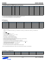
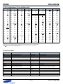
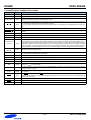
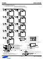
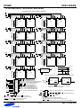
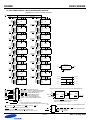
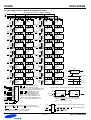
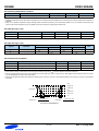
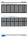
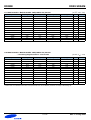
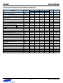
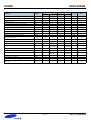
DDR2 SDRAM
RDIMM
DDR2 Registered SDRAM MODULE
240pin Registered Module based on 512Mb G-die
72-bit ECC
60FBGA with Lead-Free and Halogen-Free
(RoHS compliant)
INFORMATION IN THIS DOCUMENT IS PROVIDED IN RELATION TO SAMSUNG PRODUCTS,
AND IS SUBJECT TO CHANGE WITHOUT NOTICE. NOTHING IN THIS DOCUMENT SHALL BE
CONSTRUED AS GRANTING ANY LICENSE, EXPRESS OR IMPLIED, BY ESTOPPEL OR OTHERWISE, TO ANY INTELLECTUAL PROPERTY RIGHTS IN SAMSUNG PRODUCTS OR TECHNOLOGY. ALL INFORMATION IN THIS DOCUMENT IS PROVIDED ON AS "AS IS" BASIS WITHOUT
GUARANTEE OR WARRANTY OF ANY KIND.
1. For updates or additional information about Samsung products, contact your nearest Samsung office.
2. Samsung products are not intended for use in life support, critical care, medical, safety equipment, or similar
applications where Product failure could result in loss of life or personal or physical harm, or any military or
defense application, or any governmental procurement to which special terms or provisions may apply.
* Samsung Electronics reserves the right to change products or specification without notice.
1 of 26
Rev. 1.0 July 2008
DDR2 SDRAM
RDIMM
Table of Contents
1.0 DDR2 Registered DIMM Ordering Information ..........................................................................4
2.0 Features ........................................................................................................................................4
3.0 Address Configuration ................................................................................................................4
4.0 Pin Configurations (Front side/Back side) ................................................................................5
5.0 Pin Description ............................................................................................................................5
6.0 Input/Output Functional Description .........................................................................................6
7.0 Functional Block Diagram ...........................................................................................................7
7.1 512MB, 64Mx72 Module - M393T6553GZ3/M393T6553GZA ...............................................................7
7.2 1GB, 128Mx72 Module - M393T2953GZ3/M393T2953GZA ..................................................................8
7.3 1GB, 128Mx72 Module - M393T2950GZ3/M393T2950GZA ..................................................................9
7.4 2GB, 256Mx72 Module - M393T5750GZ3/M393T5750GZA ................................................................10
8.0 Absolute Maximum DC Ratings ................................................................................................11
9.0 AC & DC Operating Conditions ................................................................................................11
9.1 Recommended DC Operating Conditions (SSTL - 1.8) ....................................................................11
9.2 Operating Temperature Condition ...............................................................................................12
9.3 Input DC Logic Level .................................................................................................................12
9.4 Input AC Logic Level ..................................................................................................................12
9.5 AC Input Test Conditions ...........................................................................................................12
10.0 IDD Specification Parameters Definition ...............................................................................13
11.0 Operating Current Table : .......................................................................................................14
11.1 M393T6553GZ3 / M393T6553GZA : 512MB(64Mx8 *9) Module ....................................................14
11.2 M393T6553GZ3 / M393T6553GZA : 512MB(64Mx8 *9) Module ....................................................14
11.3 M393T2953GZ3 / M393T2953GZA : 1GB(64Mx8 *18) Module ......................................................15
11.4 M393T2953GZ3 / M393T2953GZA : 1GB(64Mx8 *18) Module ......................................................15
11.5 M393T2950GZ3 / M393T2950GZA : 1GB(128Mx4 *18) Module ....................................................16
11.6 M393T2950GZ3 / M393T2950GZA : 1GB(128Mx4 *18) Module ....................................................16
11.7 M393T5750GZ3 / M393T5750GZA : 2GB(128Mx4 *36) Module ....................................................17
11.8 M393T5750GZ3 / M393T5750GZA : 2GB(128Mx4 *36) Module ....................................................17
12.0 Input/Output Capacitance .......................................................................................................18
13.0 Electrical Characteristics & AC Timing for DDR2-800/667/533/400 .....................................18
13.1 Refresh Parameters by Device Density ...................................................................................18
13.2 Speed Bins and CL, tRCD, tRP, tRC and tRAS for Corresponding Bin .........................................18
13.3 Timing parameters by speed grade (DDR2-800 and DDR2-667)....................................................19
13.4 Timing parameters by speed grade (DDR2-533 and DDR2-400)....................................................21
14.0 Physical Dimensions ...............................................................................................................23
14.1 64Mbx8 based 64Mx72 Module (1 Rank) ..................................................................................23
14.2 64Mbx8/128Mbx4 based 128Mx72 Module (2/1 Ranks) ...............................................................24
14.3 128Mbx4 based 256Mx72 Module (2 Ranks) .............................................................................25
15.0 240 Pin DDR2 Registered DIMM Clock Topology .................................................................26
2 of 26
Rev. 1.0 July 2008
DDR2 SDRAM
RDIMM
Revision History
Revision
Month
Year
1.0
July
2008
History
- Initial Release
3 of 26
Rev. 1.0 July 2008
DDR2 SDRAM
RDIMM
1.0 DDR2 Registered DIMM Ordering Information
Part Number
Density
Organization
Component Composition
Number of Rank
Parity Register
Height
M393T6553GZ3-CD5/CC
512MB
64Mx72
64Mx8(K4T51083QG)*9EA
1
X
30.00mm
M393T6553GZA-CF7/E6
512MB
64Mx72
64Mx8(K4T51083QG)*9EA
1
O
30.00mm
M393T2953GZ3-CD5/CC
1GB
128Mx72
64Mx8(K4T51083QG)*18EA
2
X
30.00mm
M393T2953GZA-CF7/E6
1GB
128Mx72
64Mx8(K4T51083QG)*18EA
2
O
30.00mm
M393T2950GZ3-CD5/CC
1GB
128Mx72
128Mx4(K4T51043QG)*18EA
1
X
30.00mm
M393T2950GZA-CF7/E6
1GB
128Mx72
128Mx4(K4T51043QG)*18EA
1
O
30.00mm
M393T5750GZ3-CD5/CC
2GB
256Mx72
128Mx4(K4T51043QG)*36EA
2
X
30.00mm
M393T5750GZA-CF7/E6
2GB
256Mx72
128Mx4(K4T51043QG)*36EA
2
O
30.00mm
Note :
1. “Z” of Part number(11th digit) stands for Lead-Free and RoHS compliant products.
2. “3” of Part number(12th digit) stands for Dummy Pad PCB products.
3. “A” of Part number(12th digit) stands for Parity Register products.
2.0 Features
• Performance range
F7(DDR2-800)
E6(DDR2-667)
D5(DDR2-533)
CC(DDR2-400)
Unit
Speed@CL3
-
400
400
400
Mbps
Speed@CL4
533
533
533
400
Mbps
Speed@CL5
667
667
533
-
Mbps
Speed@CL6
800
-
-
-
Mbps
CL-tRCD-tRP
6-6-6
5-5-5
4-4-4
3-3-3
CK
• JEDEC standard VDD = 1.8V ± 0.1V Power Supply
• VDDQ = 1.8V ± 0.1V
• 200 MHz fCK for 400Mb/sec/pin, 267MHz fCK for 533Mb/sec/pin, 333MHz fCK for 667Mb/sec/pin, 400MHz fCK for 800Mb/sec/pin
• 4 Banks
• Posted CAS
• Programmable CAS Latency: 3, 4, 5, 6
• Programmable Additive Latency: 0, 1 , 2 , 3, 4 and 5
• Write Latency(WL) = Read Latency(RL) -1
• Burst Length: 4 , 8(Interleave/Nibble sequential)
• Programmable Sequential / Interleave Burst Mode
• Bi-directional Differential Data-Strobe (Single-ended data-strobe is an optional feature)
• Off-Chip Driver(OCD) Impedance Adjustment
• On Die Termination with selectable values(50/75/150 ohms or disable)
• Average Refresh Period 7.8us at lower than a TCASE 85°C, 3.9us at 85°C < TCASE < 95 °C
- Support High Temperature Self-Refresh rate enable feature
• Serial presence detect with EEPROM
• DDR2 SDRAM Package: 60ball FBGA - 128Mx4/64Mx8
• All of base components are Lead-Free, Halogen-Free, and RoHS compliant
Note: For detailed DDR2 SDRAM operation, please refer to Samsung’s Device operation & Timing diagram.
3.0 Address Configuration
Organization
Row Address
Column Address
Bank Address
Auto Precharge
128Mx4(512Mb) based Module
A0-A13
A0-A9,A11
BA0-BA1
A10
64Mx8(512Mb) based Module
A0-A13
A0-A9
BA0-BA1
A10
4 of 26
Rev. 1.0 July 2008
DDR2 SDRAM
RDIMM
4.0 Pin Configurations (Front side/Back side)
Pin
Front
Pin
Back
Pin
Front
Pin
Back
Pin
Front
Pin
Back
Pin
Front
Pin
Back
1
VREF
121
VSS
31
DQ19
151
VSS
61
A4
181
VDDQ
91
VSS
211
DM5/DQS14
NC/DQS14
2
VSS
122
DQ4
32
VSS
152
DQ28
62
VDDQ
182
A3
92
DQS5
212
3
DQ0
123
DQ5
33
DQ24
153
DQ29
63
A2
183
A1
93
DQS5
213
VSS
4
DQ1
124
VSS
34
DQ25
154
VSS
64
VDD
184
VDD
94
VSS
214
DQ46
DQ47
5
VSS
125
DM0/DQS9
35
VSS
155
DM3/DQS12
95
DQ42
215
6
DQS0
126
NC/DQS9
36
DQS3
156
NC/DQS12
65
VSS
185
CK0
96
DQ43
216
VSS
7
DQS0
127
VSS
37
DQS3
157
VSS
66
VSS
186
CK0
97
VSS
217
DQ52
DQ53
KEY
8
VSS
128
DQ6
38
VSS
158
DQ30
67
VDD
187
VDD
98
DQ48
218
9
DQ2
129
DQ7
39
DQ26
159
DQ31
68
NC/Par_In
188
A0
99
DQ49
219
VSS
10
DQ3
130
VSS
40
DQ27
160
VSS
69
VDD
189
VDD
100
VSS
220
RFU
RFU
11
VSS
131
DQ12
41
VSS
161
CB4
70
A10/AP
190
BA1
101
SA2
221
12
DQ8
132
DQ13
42
CB0
162
CB5
71
BA0
191
VDDQ
102
NC(TEST)
222
VSS
13
DQ9
133
VSS
43
CB1
163
VSS
72
VDDQ
192
RAS
103
VSS
223
DM6/DQS15
NC/DQS15
14
VSS
134
DM1/DQS10
44
VSS
164
DM8/DQS17
73
WE
193
S0
104
DQS6
224
15
DQS1
135
NC/DQS10
45
DQS8
165
NC/DQS17
74
CAS
194
VDDQ
105
DQS6
225
VSS
16
DQS1
136
VSS
46
DQS8
166
VSS
75
VDDQ
195
ODT0
106
VSS
226
DQ54
DQ55
17
VSS
137
RFU
47
VSS
167
CB6
76
S14
196
A13
107
DQ50
227
18
RESET
138
RFU
48
CB2
168
CB7
77
ODT1
197
VDD
108
DQ51
228
VSS
19
NC
139
VSS
49
CB3
169
VSS
78
VDDQ
198
VSS
109
VSS
229
DQ60
DQ61
20
VSS
140
DQ14
50
VSS
170
VDDQ
79
VSS
199
DQ36
110
DQ56
230
21
DQ10
141
DQ15
51
VDDQ
171
80
DQ32
200
DQ37
111
DQ57
231
VSS
22
DQ11
142
VSS
52
CKE0
172
CKE14
VDD
81
DQ33
201
VSS
112
VSS
232
DM7/DQS16
NC/DQS16
23
VSS
143
DQ20
53
VDD
173
NC
82
VSS
202
DM4/DQS13
113
DQS7
233
24
DQ16
144
DQ21
54
NC
174
83
DQS4
203
NC/DQS13
114
DQS7
234
VSS
25
DQ17
145
VSS
55
NC/Err_Out
175
NC
VDDQ
84
DQS4
204
VSS
115
VSS
235
DQ62
DQ63
26
VSS
146
DM2/DQS11
56
VDDQ
176
A12
85
VSS
205
DQ38
116
DQ58
236
27
DQS2
147
NC/DQS11
57
A11
177
A9
86
DQ34
206
DQ39
117
DQ59
237
VSS
28
DQS2
148
VSS
58
A7
178
VDD
87
DQ35
207
VSS
118
VSS
238
VDDSPD
29
VSS
149
DQ22
59
VDD
179
A8
88
VSS
208
DQ44
119
SDA
239
SA0
30
DQ18
150
DQ23
60
A5
180
A6
89
DQ40
209
120
SCL
240
SA1
90
DQ41
210
DQ45
VSS
NC = No Connect, RFU = Reserved for Future Use
1. RESET (Pin 18) is connected to both OE of PLL and Reset of register.
2. The Test pin (Pin 102) is reserved for bus analysis probes and is not connected on normal memory modules (DIMMs)
3. NC/Err_Out ( Pin 55) and NC/Par_In (Pin 68) are for optional function to check address and command parity.
4. CKE1,S1 Pin is used for double side Registered DIMM.
5.0 Pin Description
Pin Name
CK0
Description
Clock Inputs, positive line
Pin Name
ODT0~ODT1
Description
On die termination
CK0
Clock inputs, negative line
DQ0~DQ63
Data Input/Output
CKE0, CKE1
Clock Enables
CB0~CB7
Data check bits Input/Output
RAS
Row Address Strobe
DQS0~DQS8
Data strobes
CAS
Column Address Strobe
DQS0~DQS8
Data strobes, negative line
WE
Write Enable
DM(0~8),DQS(9~17)
Data Masks / Data strobes (Read)
S0, S1
Chip Selects
DQS9~DQS17
Data strobes (Read), negative line
A0~A9, A11~A13
Address Inputs
RFU
Reserved for Future Use
A10/AP
Address Input/Autoprecharge
NC
No Connect
BA0, BA1
DDR2 SDRAM Bank Address
TEST
Memory bus test tool
(Not Connect and Not Useable on DIMMs)
SCL
Serial Presence Detect (SPD) Clock Input
VDD
Core Power
SDA
SPD Data Input/Output
VDDQ
I/O Power
SA0~SA2
SPD address
VSS
Ground
Par_In
Parity bit for the Address and Control bus
VREF
Input/Output Reference
Err_Out
Parity error found in the Address and Control bus
VDDSPD
SPD Power
RESET
Register and PLL control pin
*The VDD and VDDQ pins are tied to the single power-plane on PCB.
5 of 26
Rev. 1.0 July 2008
DDR2 SDRAM
RDIMM
6.0 Input/Output Functional Description
Symbol
Type
Function
CK0
Input
Positive line of the differential pair of system clock inputs that drives input to the on-DIMM PLL.
CK0
Input
Negative line of the differential pair of system clock inputs that drives the input to the on-DIMM PLL.
CKE0~CKE1
Input
Activates the SDRAM CK signal when high and deactivates the CK signal when low. By deactivating the clocks, CKE low
initiates the Power Down mode, or the Self Refresh mode.
S0~S1
Input
Enables the associated SDRAM command decoder when low and disables decoder when high. When decoder is disabled,
new commands are ignored but previous operations continue.
These input signals also disable all outputs (except CKE and ODT) of the register(s) on the DIMM when both inputs are
high.
ODT0~ODT1
Input
I/O bus impedance control signals.
RAS, CAS, WE
Input
When sampled at the positive rising edge of the clock, CAS, RAS, and WE define the operation to be executed by the
SDRAM.
VREF
Supply
VDDQ
Supply
BA0~BA1
Input
Selects which SDRAM bank of four is activated.
Input
During a Bank Activate command cycle, Address defines the row address.
During a Read or Write command cycle, Address defines the column address. In addition to the column address, AP is
used to invoke autoprecharge operation at the end of the burst read or write cycle. If AP is high, autoprecharge is selected
and BA0, BA1 defines the bank to be precharged. If AP is low, autoprecharge is disabled. During a Precharge command
cycle, AP is used in conjunction with BA0, BA1 to control which bank(s) to precharge. If AP is high, all banks will be precharged regardless of the state of BA0 or BA1. If AP is low, BA0 and BA1 are used to define which bank to precharge.
DQ0~63,
CB0~CB7
In/Out
Data and Check Bit Input/Output pins
DM0~DM8
Input
Masks write data when high, issued concurrently with input data. Both DM and DQ have a write latency of one clock once
the write command is registered into the SDRAM.
A0~A9,A10/AP
A11~A13
Reference voltage for SSTL_18 inputs
Isolated power supply for the DDR SDRAM output buffers to provide improved noise immunity
VDD, VSS
Supply
Power and ground for the DDR SDRAM input buffers and core logic
DQS0~DQS17
In/Out
Positive line of the differential data strobe for input and output data.
DQS0~DQS17
In/Out
Negative line of the differential data strobe for input and output data.
SA0~SA2
Input
These signals are tied at the system planar to either VSS or VDDSPD to configure the serial SPD EEPROM address range.
SDA
In/Out
This bidirectional pin is used to transfer data into or out of the SPD EEPROM. A resistor must be connected from the SDA
bus line to VDDSPD to act as a pullup.
SCL
Input
This signal is used to clock data into and out of the SPD EEPROM. A resistor may be connected from the SCL bus time
to VDDSPD to act as a pullup.
VDDSPD
Supply
Serial EEPROM positive power supply (wired to a separate power pin at the connector which supports from 1.7 Volt to 3.6
Volt operation).
RESET
Input
The RESET pin is connected to the RST pin on the register and to the OE pin on the PLL. When low, all register outputs
will be driven low and the PLL clocks to the DRAMs and register(s) will be set to low level (The PLL will remain synchronized with the input clock )
Par_In
Input
Parity bit for the Address and Control bus. ( “1 “ : Odd, “0 “ : Even)
Err_Out
Input
Parity error found in the Address and Control bus
TEST
In/Out
Used by memory bus analysis tools (unused on memory DIMMs)
6 of 26
Rev. 1.0 July 2008
DDR2 SDRAM
RDIMM
7.0 Functional Block Diagram
7.1 512MB, 64Mx72 Module - M393T6553GZ3/M393T6553GZA
(populated as 1 rank of x8 DDR2 SDRAMs)
RS0
DQS0
DQS0
DM0/DQS9
NC/DQS9
DQS4
DQS4
DM4/DQS13
NC/DQS13
DQ0
DQ1
DQ2
DQ3
DQ4
DQ5
DQ6
DQ7
DM/ NU/ CS
RDQS RDQS
I/O 0
I/O 1
I/O 2
I/O 3
I/O 4
I/O 5
I/O 6
I/O 7
DQS DQS
DQ32
DQ33
DQ34
DQ35
DQ36
DQ37
DQ38
DQ39
D0
DQS1
DQS1
DM1/DQS10
NC/DQS10
DM/ NU/ CS
RDQS RDQS
I/O 0
I/O 1
I/O 2
I/O 3
I/O 4
I/O 5
I/O 6
I/O 7
DQS DQS
D4
DQS5
DQS5
DM5/DQS14
NC/DQS14
DQ8
DQ9
DQ10
DQ11
DQ12
DQ13
DQ14
DQ15
DM/ NU/ CS
RDQS RDQS
I/O 0
I/O 1
I/O 2
I/O 3
I/O 4
I/O 5
I/O 6
I/O 7
DQS DQS
DQ40
DQ41
DQ42
DQ43
DQ44
DQ45
DQ46
DQ47
D1
DQS2
DQS2
DM2/DQS11
NC/DQS11
DM/ NU/ CS
RDQS RDQS
I/O 0
I/O 1
I/O 2
I/O 3
I/O 4
I/O 5
I/O 6
I/O 7
DQS DQS
D5
DQS6
DQS6
DM6/DQS15
NC/DQS15
DQ16
DQ17
DQ18
DQ19
DQ20
DQ21
DQ22
DQ23
DM/ NU/ CS
RDQS RDQS
I/O 0
I/O 1
I/O 2
I/O 3
I/O 4
I/O 5
I/O 6
I/O 7
DQS DQS
DQ48
DQ49
DQ50
DQ51
DQ52
DQ53
DQ54
DQ55
D2
DQS3
DQS3
DM3/DQS12
NC/DQS12
DM/ NU/ CS
RDQS RDQS
I/O 0
I/O 1
I/O 2
I/O 3
I/O 4
I/O 5
I/O 6
I/O 7
DQS DQS
D6
DQS7
DQS7
DM7/DQS16
NC/DQS16
DQ24
DQ25
DQ26
DQ27
DQ28
DQ29
DQ30
DQ31
DM/ NU/ CS
RDQS RDQS
I/O 0
I/O 1
I/O 2
I/O 3
I/O 4
I/O 5
I/O 6
I/O 7
DQS DQS
DQ56
DQ57
DQ58
DQ59
DQ60
DQ61
DQ62
DQ63
D3
DQS8
DQS8
DM8/DQS17
NC/DQS17
DM/ NU/ CS
RDQS RDQS
I/O 0
I/O 1
I/O 2
I/O 3
I/O 4
I/O 5
I/O 6
I/O 7
DQS DQS
D7
Serial PD
SCL
CB0
CB1
CB2
CB3
CB4
CB5
CB6
CB7
DM/ NU/ CS
RDQS RDQS
I/O 0
I/O 1
I/O 2
I/O 3
I/O 4
I/O 5
I/O 6
I/O 7
1:1
R
E
G
I
S
T
E
R
S0*
BA0-BA1
A0-A13
RAS
CAS
WE
CKE0
ODT0
RESET
RST
DQS DQS
D8
SDA
WP A0
A1
A2
SA0 SA1 SA2
VDDSPD
Serial PD
VDD/VDDQ
D0 - D8
VREF
D0 - D8
VSS
D0 - D8
Signals for Address and Command Parity Function (M393T6553GZA)
VSS
VSS
PAR_IN
RSO-> CS : DDR2 SDRAMs D0-D8
RBA0-RBA1 -> BA0-BA1 : DDR2 SDRAMs D0-D8
RA0-RA13 -> A0-A13 : DDR2 SDRAMs D0-D8
RRAS -> RAS : DDR2 SDRAMs D0-D8
RCAS -> CAS : DDR2 SDRAMs D0-D8
RWE -> WE : DDR2 SDRAMs D0-D8
RCKE0 -> CKE : DDR2 SDRAMs D0-D8
RODT0 -> ODT0 : DDR2 SDRAMs D0-D8
C0
C1
Register
PAR_IN
100K ohms
PPO
QERR
Err_Out
The resistors on Par_In, A13, A14, A15, BA2 and the
signal line of Err_Out refer to the section: "Register
Options for Unused Address inputs"
* S0 connects to DCS and VDD connects to CSR on the register. S1, CKE1 and ODT1 are NC.
PCK7
PCK7
Note :
1. DQ-to-I/O wiring may be changed within a byte.
2. DQ/DQS/DM/CKE/S relationships must be maintained as shown.
3. Unless otherwise noted, resister values are 22 Ohms ± 5%
CK0
CK0
RESET
7 of 26
P
L
L
OE
PCK0-PCK6, PCK8, PCK9 -> CK : DDR2 SDRAMs D0-D8
PCK0-PCK6, PCK8, PCK9 -> CK : DDR2 SDRAMs D0-D8
PCK7 -> CK : Register
PCK7 -> CK : Register
Rev. 1.0 July 2008
DDR2 SDRAM
RDIMM
7.2 1GB, 128Mx72 Module - M393T2953GZ3 / M393T2953GZA
(populated as 2 rank of x8 DDR2 SDRAMs)
RS1
RS0
DQS0
DQS0
DM0/DQS9
NC/DQS9
DQS4
DQS4
DM4/DQS13
NC/DQS13
DQ0
DQ1
DQ2
DQ3
DQ4
DQ5
DQ6
DQ7
DM/ NU/ CS
RDQS RDQS
I/O 0
I/O 1
I/O 2
I/O 3
I/O 4
I/O 5
I/O 6
I/O 7
DQS DQS
DM/ NU/ CS
RDQS RDQS
I/O 0
I/O 1
I/O 2
I/O 3
I/O 4
I/O 5
I/O 6
I/O 7
D0
DQS DQS
DM/ NU/ CS
RDQS RDQS
DQ32
DQ33
DQ34
DQ35
DQ36
DQ37
DQ38
DQ39
D9
DQS1
DQS1
DM1/DQS10
NC/DQS10
I/O 0
I/O 1
I/O 2
I/O 3
I/O 4
I/O 5
I/O 6
I/O 7
DQS DQS
DM/ NU/ CS
RDQS RDQS
I/O 0
I/O 1
I/O 2
I/O 3
I/O 4
I/O 5
I/O 6
I/O 7
D4
DQS DQS
D13
DQS5
DQS5
DM5/DQS14
NC/DQS14
DQ8
DQ9
DQ10
DQ11
DQ12
DQ13
DQ14
DQ15
DM/ NU/ CS
RDQS RDQS
I/O 0
I/O 1
I/O 2
I/O 3
I/O 4
I/O 5
I/O 6
I/O 7
DQS DQS
DM/ NU/ CS
RDQS RDQS
I/O 0
I/O 1
I/O 2
I/O 3
I/O 4
I/O 5
I/O 6
I/O 7
D1
DQS DQS
D10
DQS2
DQS2
DM2/DQS11
NC/DQS11
DM/ NU/ CS
RDQS RDQS
DQ40
DQ41
DQ42
DQ43
DQ44
DQ45
DQ46
DQ47
I/O 0
I/O 1
I/O 2
I/O 3
I/O 4
I/O 5
I/O 6
I/O 7
DQS DQS
DM/ NU/ CS
RDQS RDQS
I/O 0
I/O 1
I/O 2
I/O 3
I/O 4
I/O 5
I/O 6
I/O 7
D5
DQS DQS
D14
DQS6
DQS6
DM6/DQS15
NC/DQS15
DQ16
DQ17
DQ18
DQ19
DQ20
DQ21
DQ22
DQ23
DM/ NU/ CS
RDQS RDQS
I/O 0
I/O 1
I/O 2
I/O 3
I/O 4
I/O 5
I/O 6
I/O 7
DQS DQS
DM/ NU/ CS
RDQS RDQS
I/O 0
I/O 1
I/O 2
I/O 3
I/O 4
I/O 5
I/O 6
I/O 7
D2
DQS DQS
D11
DQS3
DQS3
DM3/DQS12
NC/DQS12
DM/ NU/ CS
RDQS RDQS
DQ48
DQ49
DQ50
DQ51
DQ52
DQ53
DQ54
DQ55
I/O 0
I/O 1
I/O 2
I/O 3
I/O 4
I/O 5
I/O 6
I/O 7
DQS DQS
DM/ NU/ CS
RDQS RDQS
I/O 0
I/O 1
I/O 2
I/O 3
I/O 4
I/O 5
I/O 6
I/O 7
D6
DQS DQS
D15
DQS7
DQS7
DM7/DQS16
NC/DQS16
DQ24
DQ25
DQ26
DQ27
DQ28
DQ29
DQ30
DQ31
DM/ NU/ CS
RDQS RDQS
I/O 0
I/O 1
I/O 2
I/O 3
I/O 4
I/O 5
I/O 6
I/O 7
DQS DQS
DM/ NU/ CS
RDQS RDQS
I/O 0
I/O 1
I/O 2
I/O 3
I/O 4
I/O 5
I/O 6
I/O 7
D3
DQS DQS
D12
DQS8
DQS8
DM8/DQS17
NC/DQS17
DM/ NU/ CS
RDQS RDQS
DQ56
DQ57
DQ58
DQ59
DQ60
DQ61
DQ62
DQ63
I/O 0
I/O 1
I/O 2
I/O 3
I/O 4
I/O 5
I/O 6
I/O 7
DQS DQS
I/O 0
I/O 1
I/O 2
I/O 3
I/O 4
I/O 5
I/O 6
I/O 7
D7
Serial PD
CB0
CB1
CB2
CB3
CB4
CB5
CB6
CB7
DM/ NU/ CS
RDQS RDQS
I/O 0
I/O 1
I/O 2
I/O 3
I/O 4
I/O 5
I/O 6
I/O 7
D8
DQS DQS
DM/ NU/ CS
RDQS RDQS
I/O 0
I/O 1
I/O 2
I/O 3
I/O 4
I/O 5
I/O 6
I/O 7
DQS DQS
SCL
SDA
WP A0
D17
A1
A2
SA0 SA1 SA2
DM/ NU/ CS
RDQS RDQS
DQS DQS
D16
VDDSPD
Serial PD
VDD/VDDQ
D0 - D17
VREF
D0 - D17
VSS
D0 - D17
Signals for Address and Command Parity Function (M393T2953GZA)
C0 Register A
C0 Register B
VDD
VSS
VDD
VDD
C1
C1
RSO-> CS : DDR2 SDRAMs D0-D8
PPO
RS1-> CS : DDR2 SDRAMs D9-D17
1:2
PPO
PAR_IN
PAR_IN
PAR_IN
RBA0-RBA1 -> BA0-BA1 : DDR2 SDRAMs D0-D17
R
Err_Out
QERR
QERR
100K ohms
RA0-RA13 -> A0-A13 : DDR2 SDRAMs D0-D17
E
RRAS -> RAS : DDR2 SDRAMs D0-D17
G
The resistors on Par_In, A13, A14, A15, BA2 and the
RCAS -> CAS : DDR2 SDRAMs D0-D17
I
signal line of Err_Out refer to the section: "Register
RWE
->
WE
:
DDR2
SDRAMs
D0-D17
S
RCKE0 -> CKE : DDR2 SDRAMs D0-D8
T
Options for Unused Address inputs"
RCKE1 -> CKE : DDR2 SDRAMs D9-D17
E
RODT0 -> ODT0 : DDR2 SDRAMs D0-D8
R
CK0
PCK0-PCK6, PCK8, PCK9 -> CK : DDR2 SDRAMs D0-D17
RODT1 -> ODT1 : DDR2 SDRAMs D9-D17
P
RST
RESET**
L
PCK0-PCK6, PCK8, PCK9 -> CK : DDR2 SDRAMs D0-D17
PCK7**
CK0
L
PCK7 -> CK : Register
PCK7**
OE
RESET
PCK7 -> CK : Register
* S0 connects to DCS and S1 connects to CSR on a Register,
S1 connects to DCS and S0 connects to CSR on another Register.
Note :
1. DQ-to-I/O wiring may be changed per nibble.
** RESET, PCK7 and PCK7 connects to both Registers.
2. Unless otherwise noted, resister values are 22 Ohms ± 5%
Other signals connect to one of two Registers.
3. RS0 and RS1 alternate between the back and front sides of the DIMM
S0*
S1*
BA0-BA1
A0-A13
RAS
CAS
WE
CKE0
CKE1
ODT0
ODT1
8 of 26
Rev. 1.0 July 2008
DDR2 SDRAM
RDIMM
7.3 1GB, 128Mx72 Module - M393T2950GZ3/M393T2950GZA
(populated as 1 rank of x4 DDR2 SDRAMs)
VSS
RS0
DM0/DQS9
NC/DQS9
DQS0
DQS0
DM
DQ0
DQ1
DQ2
DQ3
DQS1
DQS1
I/O 0
I/O 1
I/O 2
I/O 3
DM
DQ8
DQ9
DQ10
DQ11
I/O 0
I/O 1
I/O 2
I/O 3
CS
DQS DQS
CS
DQS DQS
I/O 0
I/O 1
I/O 2
I/O 3
CS
DQS DQS
I/O 0
I/O 1
I/O 2
I/O 3
CS
DQS DQS
I/O 0
I/O 1
I/O 2
I/O 3
CS
DQS DQS
D4
I/O 0
I/O 1
I/O 2
I/O 3
CS
DQS DQS
DQS DQS
D12
CS
I/O 0
I/O 1
I/O 2
I/O 3
DM
DQ44
DQ45
DQ46
DQ47
D5
DQS6
DQS6
DQS DQS
D13
CS
I/O 0
I/O 1
I/O 2
I/O 3
DQS DQS
D14
DM6/DQS15
NC/DQS15
DM
I/O 0
I/O 1
I/O 2
I/O 3
CS
DQS DQS
DM
DQ52
DQ53
DQ54
DQ55
D6
DQS7
DQS7
CS
I/O 0
I/O 1
I/O 2
I/O 3
DQS DQS
Serial PD
D15
SCL
I/O 0
I/O 1
I/O 2
I/O 3
CS
DQS DQS
CS
I/O 0
I/O 1
I/O 2
I/O 3
1:2
R
E
G
I
S
T
E
R
CS
D8
DQS DQS
I/O 0
I/O 1
I/O 2
I/O 3
D16
DM
CB4
CB5
CB6
CB7
CS
I/O 0
I/O 1
I/O 2
I/O 3
DQS DQS
D17
VSS
VDD
100K ohms
VDD/VDDQ
D0 - D17
VREF
D0 - D17
VSS
D0 - D17
C0
C1
Register A
PPO
VDD
VDD
C0
C1
Register B
PAR_IN
PPO
QERR
QERR
Err_Out
The resistors on Par_In, A13, A14, A15, BA2 and the
CK0
CK0
** RESET, PCK7 and PCK7 connects to both Registers. Other
signals connect to one of two Registers. S1, CKE1 and ODT1 are NC.
Serial PD
PAR_IN
PAR_IN
signal line of Err_Out refer to the section: "Register
Note :
1. DQ-to-I/O wiring may be changed per nibble.
2. Unless otherwise noted, resister values are 22 Ohms ± 5%
* S0 connects to DCS of Register1 and CSR of Register2. CSR of
register 1 and DCS of register 2 connects to VDD.
VDDSPD
Signals for Address and Command Parity Function (M393T2950GZA)
RSO-> CS : DDR2 SDRAMs D0-D17
RBA0-RBA1 -> BA0-BA1 : DDR2 SDRAMs D0-D17
RA0-RA13 -> A0-A13 : DDR2 SDRAMs D0-D17
RRAS -> RAS : DDR2 SDRAMs D0-D17
RCAS -> CAS : DDR2 SDRAMs D0-D17
RWE -> WE : DDR2 SDRAMs D0-D17
RCKE0 -> CKE : DDR2 SDRAMs D0-D17
RODT0 -> ODT0 : DDR2 SDRAMs D0-D17
RST
PCK7**
A2
DQS DQS
DM8/DQS17
NC/DQS17
DM
A1
SA0 SA1 SA2
DM
DQ60
DQ61
DQ62
DQ63
D7
DQS8
DQS8
PCK7**
SDA
WP A0
DM7DQS16
NC/DQS16
DM
RESET**
CS
I/O 0
I/O 1
I/O 2
I/O 3
DM5/DQS14
NC/DQS14
DM
S0*
BA0-BA1
A0-A13
RAS
CAS
WE
CKE0
ODT0
DQS DQS
D11
DM
DQ36
DQ37
DQ38
DQ39
DQS5
DQS5
CB0
CB1
CB2
CB3
CS
DM4/DQS13
NC/DQS13
DM
DQ56
DQ57
DQ58
DQ59
DQS DQS
D10
I/O 0
I/O 1
I/O 2
I/O 3
DM
DQ28
DQ29
DQ30
DQ31
D3
DQS4
DQS4
DQ48
DQ49
DQ50
DQ51
CS
DM3/DQS12
NC/DQS12
DM
DQ40
DQ41
DQ42
DQ43
DQS DQS
D9
I/O 0
I/O 1
I/O 2
I/O 3
DM
DQ20
DQ21
DQ22
DQ23
D2
DQS3
DQS3
DQ32
DQ33
DQ34
DQ35
CS
DM2/DQS11
NC/DQS11
DM
DQ24
DQ25
DQ26
DQ27
I/O 0
I/O 1
I/O 2
I/O 3
DM
DQ12
DQ13
DQ14
DQ15
D1
DQS2
DQS2
DQ16
DQ17
DQ18
DQ19
DM
DQ4
DQ5
DQ6
DQ7
DM1/DQS10
NC/DQS10
D0
RESET
9 of 26
Options for Unused Address inputs"
P
L
L
OE
PCK0-PCK6, PCK8, PCK9 -> CK : DDR2 SDRAMs D0-D8
PCK0-PCK6, PCK8, PCK9 -> CK : DDR2 SDRAMs D0-D8
PCK7 -> CK : Register
PCK7 -> CK : Register
Rev. 1.0 July 2008
DDR2 SDRAM
RDIMM
7.4 2GB, 256Mx72 Module - M393T5750GZ3/M393T5750GZA
(populated as 2 rank of x4 DDR2 SDRAMs)
VSS
RS1
RS0
DM0/DQS9
NC/DQS9
DQS0
DQS0
DM
DQ0
DQ1
DQ2
DQ3
DQS1
DQS1
DM
DQ8
DQ9
DQ10
DQ11
CS
DQS DQS
I/O 0
I/O 1 D0
I/O 2
I/O 3
CS
DM/
CS
DQS DQS
I/O 0
I/O 1 D18
I/O 2
I/O 3
DQS DQS
I/O 0
I/O 1 D1
I/O 2
I/O 3
DM/
CS
DQS DQS
CS
DQS DQS
I/O 0
I/O 1 D2
I/O 2
I/O 3
DM/
CS
DQS DQS
CS
DQS DQS
I/O 0
I/O 1 D3
I/O 2
I/O 3
DM
CS
DM
DQS DQS
CS
DQS DQS
CS
DQS DQS
I/O 0
I/O 1 D28
I/O 2
I/O 3
CS
DM
DQS DQS
I/O 0
I/O 1 D11
I/O 2
I/O 3
DM
DQ28
DQ29
DQ30
DQ31
DM
CS
DQS DQS
CS
DQS DQS
I/O 0
I/O 1 D29
I/O 2
I/O 3
CS
DM
DQS DQS
I/O 0
I/O 1 D12
I/O 2
I/O 3
DM
DQ36
DQ37
DQ38
DQ39
I/O 0
I/O 1 D22
I/O 2
I/O 3
I/O 0
I/O 1 D4
I/O 2
I/O 3
DQS5
DQS5
CS
DQS DQS
I/O 0
I/O 1 D30
I/O 2
I/O 3
CS
DM
DQS DQS
CS
DQS DQS
I/O 0
I/O 1 D31
I/O 2
I/O 3
I/O 0
I/O 1 D13
I/O 2
I/O 3
DM5/DQS14
NC/DQS14
DM
CS
DQS DQS
I/O 0
I/O 1 D5
I/O 2
I/O 3
DM
CS
DQS DQS
DM
DQ44
DQ45
DQ46
DQ47
I/O 0
I/O 1 D23
I/O 2
I/O 3
DQS6
DQS6
CS
DM
DQS DQS
I/O 0
I/O 1 D14
I/O 2
I/O 3
CS
DQS DQS
I/O 0
I/O 1 D32
I/O 2
I/O 3
DM6/DQS15
NC/DQS15
DM
CS
DQS DQS
I/O 0
I/O 1 D6
I/O 2
I/O 3
DM
CS
DQS DQS
DM
DQ52
DQ53
DQ54
DQ55
I/O 0
I/O 1 D24
I/O 2
I/O 3
DQS7
DQS7
CS
DM
DQS DQS
I/O 0
I/O 1 D15
I/O 2
I/O 3
CS
DQS DQS
I/O 0
I/O 1 D33
I/O 2
I/O 3
Serial PD
DM7DQS16
NC/DQS16
DM
CS
DQS DQS
I/O 0
I/O 1 D7
I/O 2
I/O 3
DM
CS
DQS DQS
SCL
DM
DQ60
DQ61
DQ62
DQ63
I/O 0
I/O 1 D25
I/O 2
I/O 3
DQS8
DQS8
CS
DM
DQS DQS
I/O 0
I/O 1 D16
I/O 2
I/O 3
CS
DQS DQS
I/O 0
I/O 1 D34
I/O 2
I/O 3
CS
I/O 0
I/O 1 D8
I/O 2
I/O 3
S0*
DQS DQS
DM
CS
DQS DQS
I/O 0
I/O 1 D26
I/O 2
I/O 3
DM
CB4
CB5
CB6
CB7
CS
DM
DQS DQS
CS
DQS DQS
I/O 0
I/O 1 D35
I/O 2
I/O 3
I/O 0
I/O 1 D17
I/O 2
I/O 3
SDA
WP A0
A1
A2
SA0 SA1 SA2
DM8/DQS17
NC/DQS17
DM
CB0
CB1
CB2
CB3
DQS DQS
DM4/DQS13
NC/DQS13
DM
DQ56
DQ57
DQ58
DQ59
DM
DQS DQS
I/O 0
I/O 1 D10
I/O 2
I/O 3
DQ20
DQ21
DQ22
DQ23
I/O 0
I/O 1 D21
I/O 2
I/O 3
DQS4
DQS4
DQ48
DQ49
DQ50
DQ51
CS
CS
I/O 0
I/O 1 D27
I/O 2
I/O 3
DM3/DQS12
NC/DQS12
DM
DQ40
DQ41
DQ42
DQ43
DM
I/O 0
I/O 1 D20
I/O 2
I/O 3
DQS3
DQS3
DQ32
DQ33
DQ34
DQ35
DM
DQS DQS
DM2/DQS11
NC/DQS11
DM
DQ24
DQ25
DQ26
DQ27
CS
I/O 0
I/O 1 D9
I/O 2
I/O 3
DQ12
DQ13
DQ14
DQ15
I/O 0
I/O 1 D19
I/O 2
I/O 3
DQS2
DQS2
DQ16
DQ17
DQ18
DQ19
DM
DQ4
DQ5
DQ6
DQ7
DM1/DQS10
NC/DQS10
VDDSPD
Serial PD
VDD/VDDQ
D0 - D35
VREF
D0 - D35
VSS
D0 - D35
RSO-> CS : DDR2 SDRAMs D0-D17
S1*
BA0-BA1
A0-A13
RAS
CAS
WE
CKE0
CKE1
ODT0
ODT1
RESET**
1:2
R
E
G
I
S
T
E
R
RS1-> CS : DDR2 SDRAMs D18-D35
RBA0-RBA1 -> BA0-BA1 : DDR2 SDRAMs D0-D35
RA0-RA13 -> A0-A13 : DDR2 SDRAMs D0-D35
RRAS -> RAS : DDR2 SDRAMs D0-D35
RCAS -> CAS : DDR2 SDRAMs D0-D35
RWE -> WE : DDR2 SDRAMs D0-D35
RCKE0 -> CKE : DDR2 SDRAMs D0-D17
RCKE1 -> CKE : DDR2 SDRAMs D18-D35
RODT0 -> ODT0 : DDR2 SDRAMs D0-D17
RODT1 -> ODT1 : DDR2 SDRAMs D18-D35
Signals for Address and Command Parity Function (M393T5750GZA)
VSS
VDD
C0
C1
Register A
PAR_IN
PAR_IN
100K ohms
PPO
VDD
VDD
C0
C1
Register B
PAR_IN
QERR
PPO
QERR
Err_Out
The resistors on Par_In, A13, A14, A15, BA2 and the
signal line of Err_Out refer to the section: "Register
RST
Options for Unused Address inputs"
PCK7**
PCK7**
* S0 connects to DCS and S1 connects to CSR on a pair of Registers,
S1 connects to DCS and S0 connects to CSR on another pair of Registers.
** RESET, PCK7 and PCK7 connects to all Registers.
Other signals connect to one pair of four Registers.
CK0
CK0
RESET
10 of 26
P
L
L
OE
PCK0-PCK6, PCK8, PCK9 -> CK : DDR2 SDRAMs D0-D35
PCK0-PCK6, PCK8, PCK9 -> CK : DDR2 SDRAMs D0-D35
PCK7 -> CK : Register
PCK7 -> CK : Register
Rev. 1.0 July 2008
DDR2 SDRAM
RDIMM
8.0 Absolute Maximum DC Ratings
Symbol
Rating
Units
Notes
Voltage on VDD pin relative to VSS
- 1.0 V ~ 2.3 V
V
1
VDDQ
Voltage on VDDQ pin relative to VSS
- 0.5 V ~ 2.3 V
V
1
VDDL
Voltage on VDDL pin relative to VSS
- 0.5 V ~ 2.3 V
V
1
Voltage on any pin relative to VSS
- 0.5 V ~ 2.3 V
V
1
-55 to +100
°C
1, 2
VDD
VIN, VOUT
TSTG
Parameter
Storage Temperature
Note :
1. Stresses greater than those listed under “Absolute Maximum Ratings” may cause permanent damage to the device. This is a stress rating only and
functional operation of the device at these or any other conditions above those indicated in the operational sections of this specification is not implied.
Exposure to absolute maximum rating conditions for extended periods may affect reliability.
2. Storage Temperature is the case surface temperature on the center/top side of the DRAM. For the measurement conditions, please refer to JESD51-2
standard.
9.0 AC & DC Operating Conditions
9.1 Recommended DC Operating Conditions (SSTL - 1.8)
Symbol
Parameter
Rating
Min.
Typ.
Max.
Units
Notes
VDD
Supply Voltage
1.7
1.8
1.9
V
VDDL
Supply Voltage for DLL
1.7
1.8
1.9
V
4
VDDQ
Supply Voltage for Output
1.7
1.8
1.9
V
4
VREF
Input Reference Voltage
0.49*VDDQ
0.50*VDDQ
0.51*VDDQ
mV
1,2
Termination Voltage
VREF-0.04
VREF
VREF+0.04
V
3
VTT
Note : There is no specific device VDD supply voltage requirement for SSTL-1.8 compliance. However under all conditions VDDQ must be less than or equal
to VDD.
1. The value of VREF may be selected by the user to provide optimum noise margin in the system. Typically the value of VREF is expected to be about 0.5
x VDDQ of the transmitting device and VREF is expected to track variations in VDDQ.
2. Peak to peak AC noise on VREF may not exceed +/-2% VREF(DC).
3. VTT of transmitting device must track VREF of receiving device.
4. AC parameters are measured with VDD, VDDQ and VDDL tied together.
11 of 26
Rev. 1.0 July 2008
DDR2 SDRAM
RDIMM
9.2 Operating Temperature Condition
Symbol
Parameter
Rating
Units
Notes
TOPER
Operating Temperature
0 to 95
°C
1, 2
Note :
1. Operating Temperature is the case surface temperature on the center/top side of the DRAM. For the measurement conditions, please refer to JESD51.2
standard.
2. At 85 - 95 °C operation temperature range, doubling refresh commands in frequency to a 32ms period ( tREFI=3.9 us ) is required, and to enter to self
refresh mode at this temperature range, an EMRS command is required to change internal refresh rate.
9.3 Input DC Logic Level
Symbol
Parameter
Min.
Max.
Units
VIH(DC)
DC input logic high
VREF + 0.125
VDDQ + 0.3
V
VIL(DC)
DC input logic low
- 0.3
VREF - 0.125
V
Notes
9.4 Input AC Logic Level
Symbol
Parameter
VIH(AC)
AC input logic high
VIL(AC)
AC input logic low
DDR2-400, DDR2-533
Min.
DDR2-667, DDR2-800
Max.
Min.
VREF + 0.250
-
VREF + 0.200
-
VREF - 0.250
Units
Max.
V
VREF - 0.200
V
9.5 AC Input Test Conditions
Symbol
VREF
VSWING(MAX)
SLEW
Condition
Input reference voltage
Value
Units
Notes
0.5 * VDDQ
V
1
Input signal maximum peak to peak swing
1.0
V
1
Input signal minimum slew rate
1.0
V/ns
2, 3
Note :
1. Input waveform timing is referenced to the input signal crossing through the VIH/IL(AC) level applied to the device under test.
2. The input signal minimum slew rate is to be maintained over the range from VREF to VIH(AC) min for rising edges and the range from VREF to VIL(AC)
max for falling edges as shown in the below figure.
3. AC timings are referenced with input waveforms switching from VIL(AC) to VIH(AC) on the positive transitions and VIH(AC) to VIL(AC) on the negative
transitions.
VDDQ
VIH(AC) min
VIH(DC) min
VSWING(MAX)
VREF
VIL(DC) max
VIL(AC) max
delta TF
Falling Slew =
delta TR
VREF - VIL(AC) max
delta TF
Rising Slew =
VSS
VIH(AC) min - VREF
delta TR
< AC Input Test Signal Waveform >
12 of 26
Rev. 1.0 July 2008
DDR2 SDRAM
RDIMM
10.0 IDD Specification Parameters Definition
(IDD values are for full operating range of Voltage and Temperature)
Symbol
Proposed Conditions
Units
IDD0
Operating one bank active-precharge current;
tCK = tCK(IDD), tRC = tRC(IDD), tRAS = tRASmin(IDD); CKE is HIGH, CS is HIGH between valid commands;
Address bus inputs are SWITCHING; Data bus inputs are SWITCHING
mA
IDD1
Operating one bank active-read-precharge current;
IOUT = 0mA; BL = 4, CL = CL(IDD), AL = 0; tCK = tCK(IDD), tRC = tRC (IDD), tRAS = tRASmin(IDD), tRCD =
tRCD(IDD); CKE is HIGH, CS is HIGH between valid commands; Address bus inputs are SWITCHING; Data pattern
is same as IDD4W
mA
IDD2P
Precharge power-down current;
All banks idle; tCK = tCK(IDD); CKE is LOW; Other control and address bus inputs are STABLE; Data bus inputs are
FLOATING
mA
IDD2Q
Precharge quiet standby current;
All banks idle; tCK = tCK(IDD); CKE is HIGH, CS is HIGH; Other control and address bus inputs are STABLE; Data
bus inputs are FLOATING
mA
IDD2N
Precharge standby current;
All banks idle; tCK = tCK(IDD); CKE is HIGH, CS is HIGH; Other control and address bus inputs are SWITCHING;
Data bus inputs are SWITCHING
mA
IDD3P
Fast PDN Exit MRS(12) = 0mA
Active power-down current;
All banks open; tCK = tCK(IDD); CKE is LOW; Other control and address bus
Slow PDN Exit MRS(12) = 1mA
inputs are STABLE; Data bus inputs are FLOATING
IDD3N
Active standby current;
All banks open; tCK = tCK(IDD), tRAS = tRASmax(IDD), tRP = tRP(IDD); CKE is HIGH, CS is HIGH between valid
commands; Other control and address bus inputs are SWITCHING; Data bus inputs are SWITCHING
mA
IDD4W
Operating burst write current;
All banks open, Continuous burst writes; BL = 4, CL = CL(IDD), AL = 0; tCK = tCK(IDD), tRAS = tRASmax(IDD), tRP
= tRP(IDD); CKE is HIGH, CS is HIGH between valid commands; Address bus inputs are SWITCHING; Data bus
inputs are SWITCHING
mA
IDD4R
Operating burst read current;
All banks open, Continuous burst reads, IOUT = 0mA; BL = 4, CL = CL(IDD), AL = 0; tCK = tCK(IDD), tRAS = tRASmax(IDD), tRP = tRP(IDD); CKE is HIGH, CS is HIGH between valid commands; Address bus inputs are SWITCHING; Data pattern is same as IDD4W
mA
IDD5B
Burst auto refresh current;
tCK = tCK(IDD); Refresh command at every tRFC(IDD) interval; CKE is HIGH, CS is HIGH between valid commands;
Other control and address bus inputs are SWITCHING; Data bus inputs are SWITCHING
mA
mA
mA
Low Power
mA
Self refresh current;
CK and CK at 0V; CKE ≤ 0.2V; Other control and address bus inputs are
FLOATING; Data bus inputs are FLOATING
IDD7
Operating bank interleave read current;
All bank interleaving reads, IOUT = 0mA; BL = 4, CL = CL(IDD), AL = tRCD(IDD)-1*tCK(IDD); tCK = tCK(IDD), tRC =
tRC(IDD), tRRD = tRRD(IDD), tFAW = tFAW(IDD), tRCD = 1*tCK(IDD); CKE is HIGH, CS is HIGH between valid
commands; Address bus inputs are STABLE during DESELECTs; Data pattern is same as IDD4R; Refer to the following page for detailed timing conditions
13 of 26
mA
Normal
IDD6
Note
mA
Rev. 1.0 July 2008
DDR2 SDRAM
RDIMM
11.0 Operating Current Table :
11.1 M393T6553GZ3 / M393T6553GZA : 512MB(64Mx8 *9) Module
(TA=0oC, VDD= 1.9V)
Symbol
F7(800@CL=6)
E6(667@CL=5)
D5(533@CL=4)
CC(400@CL=3)
Units
IDD0
765
675
675
630
mA
IDD1
855
810
765
765
mA
IDD2P
72
72
72
72
mA
IDD2Q
315
315
270
270
mA
IDD2N
360
360
315
315
mA
IDD3P-F
270
270
270
270
mA
IDD3P-S
108
108
108
108
mA
IDD3N
540
495
450
450
mA
IDD4W
990
900
765
720
mA
IDD4R
1260
1170
945
855
mA
IDD5B
990
945
945
900
mA
IDD6*
72
72
72
72
mA
IDD7
1890
1575
1575
1575
mA
Notes
* Module IDD was calculated on the basis of component IDD and can be differently measured according to DQ loading cap.
11.2 M393T6553GZ3 / M393T6553GZA : 512MB(64Mx8 *9) Module
- considering Register and PLL current value
(TA=0oC, VDD= 1.9V)
Symbol
F7(800@CL=6)
E6(667@CL=5)
D5(533@CL=4)
CC(400@CL=3)
Units
IDD0
1355
1175
1085
950
mA
IDD1
1495
1360
1225
1135
mA
IDD2P
552
512
472
432
mA
IDD2Q
845
775
660
590
mA
IDD2N
840
780
675
615
mA
IDD3P-F
820
740
660
580
mA
IDD3P-S
658
578
498
418
mA
mA
IDD3N
1080
965
850
780
IDD4W
1510
1350
1145
1030
mA
IDD4R
1850
1680
1375
1205
mA
IDD5B
1660
1495
1375
1210
mA
IDD6*
72
72
72
72
mA
IDD7
2580
2155
2045
1935
mA
Notes
* IDD6 = DRAM current + standby current of PLL and Register
** Module IDD was calculated on the basis of component IDD and can be differently measured according to DQ loading cap.
14 of 26
Rev. 1.0 July 2008
DDR2 SDRAM
RDIMM
11.3 M393T2953GZ3 / M393T2953GZA : 1GB(64Mx8 *18) Module
Symbol
(TA=0oC, VDD= 1.9V)
F7(800@CL=6)
E6(667@CL=5)
D5(533@CL=4)
CC(400@CL=3)
Units
IDD0
1125
1035
990
945
mA
IDD1
1215
1170
1080
1080
mA
IDD2P
144
144
144
144
mA
IDD2Q
630
630
540
540
mA
IDD2N
720
720
630
630
mA
mA
IDD3P-F
540
540
540
540
IDD3P-S
216
216
216
216
mA
IDD3N
900
855
765
765
mA
IDD4W
1350
1260
1080
1035
mA
IDD4R
1620
1530
1260
1170
mA
IDD5B
1350
1305
1260
1215
mA
IDD6*
144
144
144
144
mA
IDD7
2250
1935
1890
1890
mA
Notes
* Module IDD was calculated on the basis of component IDD and can be differently measured according to DQ loading cap.
11.4 M393T2953GZ3 / M393T2953GZA : 1GB(64Mx8 *18) Module
(TA=0oC, VDD= 1.9V)
- considering Register and PLL current value
Symbol
F7(800@CL=6)
E6(667@CL=5)
D5(533@CL=4)
CC(400@CL=3)
Units
IDD0
1815
1625
1480
1335
mA
IDD1
1985
1830
1630
1520
mA
IDD2P
784
724
664
604
mA
IDD2Q
1340
1250
1070
980
mA
IDD2N
1290
1220
1060
990
mA
IDD3P-F
1270
1170
1070
970
mA
IDD3P-S
946
846
746
646
mA
IDD3N
1460
1345
1185
1115
mA
IDD4W
2000
1820
1550
1415
mA
IDD4R
2410
2210
1830
1630
mA
IDD5B
2180
1985
1790
1595
mA
IDD6*
144
144
144
144
mA
IDD7
3280
2805
2600
2440
mA
Notes
* IDD6 = DRAM current + standby current of PLL and Register
** Module IDD was calculated on the basis of component IDD and can be differently measured according to DQ loading cap.
15 of 26
Rev. 1.0 July 2008
DDR2 SDRAM
RDIMM
11.5 M393T2950GZ3 / M393T2950GZA : 1GB(128Mx4 *18) Module
(TA=0oC, VDD= 1.9V)
Symbol
F7(800@CL=6)
E6(667@CL=5)
D5(533@CL=4)
CC(400@CL=3)
Units
IDD0
1440
1350
1350
1350
mA
IDD1
1620
1530
1530
1530
mA
IDD2P
144
144
144
144
mA
IDD2Q
630
630
540
540
mA
IDD2N
720
720
630
630
mA
IDD3P-F
540
540
540
540
mA
IDD3P-S
216
216
216
216
mA
IDD3N
990
990
900
900
mA
IDD4W
2070
1800
1350
1350
mA
IDD4R
2250
1980
1530
1530
mA
IDD5B
2070
1980
1890
1890
mA
IDD6*
144
144
144
144
mA
IDD7
3780
3150
3150
3150
mA
Notes
* Module IDD was calculated on the basis of component IDD and can be differently measured according to DQ loading cap.
11.6 M393T2950GZ3 / M393T2950GZA : 1GB(128Mx4 *18) Module
- considering Register and PLL current value
(TA=0oC, VDD= 1.9V)
Symbol
F7(800@CL=6)
E6(667@CL=5)
D5(533@CL=4)
CC(400@CL=3)
Units
IDD0
2130
1940
1840
1740
mA
IDD1
2390
2190
2080
1970
mA
IDD2P
784
724
664
604
mA
IDD2Q
1340
1250
1070
980
mA
IDD2N
1290
1220
1060
990
mA
IDD3P-F
1270
1170
1070
970
mA
IDD3P-S
946
846
746
646
mA
IDD3N
1550
1480
1320
1250
mA
IDD4W
2720
2360
1820
1730
mA
IDD4R
3040
2660
2100
1990
mA
IDD5B
2900
2660
2420
2270
mA
IDD6*
144
144
144
144
mA
IDD7
4810
4020
3860
3700
mA
Notes
* IDD6 = DRAM current + standby current of PLL and Register
** Module IDD was calculated on the basis of component IDD and can be differently measured according to DQ loading cap.
16 of 26
Rev. 1.0 July 2008
DDR2 SDRAM
RDIMM
11.7 M393T5750GZ3 / M393T5750GZA : 2GB(128Mx4 *36) Module
(TA=0oC, VDD= 1.9V)
Symbol
F7(800@CL=6)
E6(667@CL=5)
D5(533@CL=4)
CC(400@CL=3)
Units
IDD0
2160
2070
1980
1980
mA
IDD1
2340
2250
2160
2160
mA
IDD2P
288
288
288
288
mA
IDD2Q
1260
1260
1080
1080
mA
IDD2N
1440
1440
1260
1260
mA
IDD3P-F
1080
1080
1080
1080
mA
IDD3P-S
432
432
432
432
mA
IDD3N
1710
1710
1530
1530
mA
IDD4W
2790
2520
1980
1980
mA
IDD4R
2970
2700
2160
2160
mA
IDD5B
2790
2700
2520
2520
mA
IDD6*
288
288
288
288
mA
IDD7
4500
3870
3780
3780
mA
Notes
* Module IDD was calculated on the basis of component IDD and can be differently measured according to DQ loading cap.
11.8 M393T5750GZ3 / M393T5750GZA : 2GB(128Mx4 *36) Module
- considering Register and PLL current value
(TA=0oC, VDD= 1.9V)
Symbol
F7(800@CL=6)
E6(667@CL=5)
D5(533@CL=4)
CC(400@CL=3)
Units
IDD0
3180
2940
2700
2550
mA
mA
IDD1
3500
3250
3000
2840
IDD2P
1238
1148
1058
968
mA
IDD2Q
2320
2180
1860
1720
mA
IDD2N
2240
2140
1860
1760
mA
IDD3P-F
2170
2020
1870
1720
mA
IDD3P-S
1522
1372
1222
1072
mA
IDD3N
2500
2400
2120
2020
mA
IDD4W
3780
3370
2690
2550
mA
IDD4R
4060
3640
2950
2800
mA
IDD5B
4010
3700
3300
3080
mA
IDD6*
288
288
288
288
mA
IDD7
6210
5320
4970
4710
mA
Notes
* IDD6 = DRAM current + standby current of PLL and Register
** Module IDD was calculated on the basis of component IDD and can be differently measured according to DQ loading cap.
17 of 26
Rev. 1.0 July 2008
DDR2 SDRAM
RDIMM
12.0 Input/Output Capacitance
(VDD=1.8V, VDDQ=1.8V, TA=25oC)
Parameter
Min
Symbol
Part-Number
Max
M393T6553GZ3
M393T6553GZA
Min
Max
Min
M393T2953GZ3
M393T2953GZA
Max
M393T2950GZ3
M393T2950GZA
Min
Max
M393T5750GZ3
M393T5750GZA
Input capacitance, CK and CK
CCK
-
11
-
11
-
11
-
11
Input capacitance, CKE and CS
CI1
-
12
-
12
-
12
-
12
Input capacitance, Address, RAS,CAS,WE
CI2
-
12
-
12
-
12
-
12
Input/output capacitance, DQ, DM, DQS, DQS
CIO
-
10
-
10
-
10
-
10
Units
pF
* DM is internally loaded to match DQ and DQS identically.
13.0 Electrical Characteristics & AC Timing for DDR2-800/667/533/400
(0 °C < TOPER < 95 °C; VDDQ = 1.8V + 0.1V; VDD = 1.8V + 0.1V)
13.1 Refresh Parameters by Device Density
Parameter
Symbol
256Mb
512Mb
1Gb
2Gb
4Gb
Units
tRFC
75
105
127.5
195
327.5
ns
0 °C ≤ TCASE ≤ 85°C
7.8
7.8
7.8
7.8
7.8
µs
85 °C < TCASE ≤ 95°C
3.9
3.9
3.9
3.9
3.9
µs
Refresh to active/Refresh command time
Average periodic refresh interval
tREFI
13.2 Speed Bins and CL, tRCD, tRP, tRC and tRAS for Corresponding Bin
Speed
DDR2-800(F7)
DDR2-667(E6)
DDR2-533(D5)
DDR2-400(CC)
Bin(CL - tRCD - tRP)
6-6-6
5-5-5
4-4-4
3-3-3
Units
Parameter
min
max
min
max
min
max
min
max
tCK, CL=3
-
-
5
8
5
8
5
8
ns
tCK, CL=4
3.75
8
3.75
8
3.75
8
5
8
ns
tCK, CL=5
3
8
3
8
3.75
8
-
-
ns
tCK, CL=6
2.5
8
-
-
-
-
-
-
ns
tRCD
15
-
15
-
15
-
15
-
ns
tRP
15
-
15
-
15
-
15
-
ns
tRC
60
-
60
-
60
-
55
-
ns
tRAS
45
70000
45
70000
45
70000
40
70000
ns
18 of 26
Rev. 1.0 July 2008
DDR2 SDRAM
RDIMM
13.3 Timing parameters by speed grade (DDR2-800 and DDR2-667)
(Refer to notes for informations related to this table at the component datasheet)
Parameter
Symbol
DDR2-800
DDR2-667
min
max
min
max
Units
Notes
40
DQ output access time from CK/CK
tAC
-400
400
-450
450
ps
DQS output access time from CK/CK
tDQSCK
-350
350
-400
400
ps
40
Average clock HIGH pulse width
tCH(avg)
0.48
0.52
0.48
0.52
tCK(avg)
35,36
Average clock LOW pulse width
tCL(avg)
0.48
0.52
0.48
0.52
tCK(avg)
35,36
Min(tCL(abs),
tCH(abs))
x
Min(tCL(abs),
tCH(abs))
x
ps
37
CK half pulse period
tHP
Average clock period
tCK(avg)
2500
8000
3000
8000
ps
35,36
DQ and DM input hold time
tDH(base)
125
x
175
x
ps
6,7,8,21,28,31
DQ and DM input setup time
tDS(base)
50
x
100
x
ps
6,7,8,20,28,31
Control & Address input pulse width for each input
tIPW
0.6
x
0.6
x
tCK(avg)
DQ and DM input pulse width for each input
tDIPW
0.35
x
0.35
x
tCK(avg)
Data-out high-impedance time from CK/CK
tHZ
x
tAC(max)
x
tAC(max)
ps
18,40
DQS/DQS low-impedance time from CK/CK
tLZ(DQS)
tAC(min)
tAC(max)
tAC(min)
tAC(max)
ps
18,40
DQ low-impedance time from CK/CK
tLZ(DQ)
2* tAC(min)
tAC(max)
2* tAC(min)
tAC(max)
ps
18,40
DQS-DQ skew for DQS and associated DQ signals
tDQSQ
x
200
x
240
ps
13
DQ hold skew factor
tQHS
x
300
x
340
ps
38
DQ/DQS output hold time from DQS
tQH
tHP - tQHS
x
tHP - tQHS
x
ps
39
DQS latching rising transitions to associated clock edges
tDQSS
- 0.25
0.25
-0.25
0.25
tCK(avg)
30
DQS input HIGH pulse width
tDQSH
0.35
x
0.35
x
tCK(avg)
DQS input LOW pulse width
tDQSL
0.35
x
0.35
x
tCK(avg)
DQS falling edge to CK setup time
tDSS
0.2
x
0.2
x
tCK(avg)
30
DQS falling edge hold time from CK
tDSH
0.2
x
0.2
x
tCK(avg)
30
Mode register set command cycle time
tMRD
2
x
2
x
nCK
MRS command to ODT update delay
tMOD
0
12
0
12
ns
32
Write postamble
tWPST
0.4
0.6
0.4
0.6
tCK(avg)
10
Write preamble
tWPRE
0.35
x
0.35
x
tCK(avg)
Address and control input hold time
tIH(base)
250
x
275
x
ps
5,7,9,23,29
Address and control input setup time
tIS(base)
175
x
200
x
ps
5,7,9,22,29
Read preamble
tRPRE
0.9
1.1
0.9
1.1
tCK(avg)
19,41
Read postamble
tRPST
0.4
0.6
0.4
0.6
tCK(avg)
19,42
Activate to activate command period for 1KB page size products tRRD
7.5
x
7.5
x
ns
4,32
Activate to activate command period for 2KB page size products tRRD
10
x
10
x
ns
4,32
19 of 26
Rev. 1.0 July 2008
DDR2 SDRAM
RDIMM
Parameter
Symbol
Four Activate Window for 1KB page size products
Four Activate Window for 2KB page size products
DDR2-800
DDR2-667
Units
Notes
x
ns
32
x
ns
32
2
x
nCK
x
15
x
ns
x
WR + tnRP
x
nCK
33
7.5
x
7.5
x
ns
24,32
7.5
x
7.5
x
ns
3,32
tXSNR
tRFC + 10
x
tRFC + 10
x
ns
32
tXSRD
200
x
200
x
nCK
tXP
2
x
2
x
nCK
tXARD
2
x
2
x
nCK
1
8 - AL
x
7 - AL
x
nCK
1,2
27
min
max
min
max
tFAW
35
x
37.5
tFAW
45
x
50
CAS to CAS command delay
tCCD
2
x
Write recovery time
tWR
15
Auto precharge write recovery + precharge time
tDAL
WR + tnRP
Internal write to read command delay
tWTR
Internal read to precharge command delay
tRTP
Exit self refresh to a non-read command
Exit self refresh to a read command
Exit precharge power down to any command
Exit active power down to read command
Exit active power down to read command
(slow exit, lower power)
tXARDS
32
CKE minimum pulse width (HIGH and LOW pulse width)
tCKE
3
x
3
x
nCK
ODT turn-on delay
tAOND
2
2
2
2
nCK
16
ODT turn-on
tAON
tAC(min)
tAC(max)+0.7
tAC(min)
tAC(max)+0.7
ns
6,16,40
ODT turn-on (Power-Down mode)
tAONPD
tAC(min)+2
2*tCK(avg)
+tAC(max)+1
tAC(min)+2
2*tCK(avg)
+tAC(max)+1
ns
2.5
2.5
2.5
2.5
nCK
17,45
tAC(min)
tAC(max)+0.6
tAC(min)
tAC(max)+0.6
ns
17,43,45
tAC(min)+2
2.5*tCK(avg)+
tAC(max)+1
tAC(min)+2
2.5*tCK(avg)+
tAC(max)+1
ns
tANPD
3
x
3
x
nCK
tAXPD
8
x
8
x
nCK
tOIT
0
12
0
12
ns
32
x
tIS+tCK(avg)
+tIH
x
ns
15
ODT turn-off delay
tAOFD
ODT turn-off
tAOF
ODT turn-off (Power-Down mode)
tAOFPD
ODT to power down entry latency
ODT power down exit latency
OCD drive mode output delay
Minimum time clocks remains ON after CKE asynchronously
tDelay
drops LOW
tIS+tCK(avg)
+tIH
20 of 26
Rev. 1.0 July 2008
DDR2 SDRAM
RDIMM
13.4 Timing parameters by speed grade (DDR2-533 and DDR2-400)
(Refer to notes for informations related to this table at the component datasheet)
Parameter
Symbol
DDR2-533
DDR2-400
min
max
min
max
-500
500
-600
600
Units
Notes
DQ output access time from CK/CK
tAC
DQS output access time from CK/CK
tDQSCK
-450
450
-500
500
ps
CK HIGH pulse width
tCH
0.45
0.55
0.45
0.55
tCK
CK LOW pulse width
tCL
0.45
0.55
0.45
0.55
tCK
CK half pulse period
tHP
Min(tCL, tCH)
x
Min(tCL, tCH)
x
ps
Clock cycle time, CL=x
tCK
3750
8000
5000
8000
ps
15
DQ and DM input hold time (differential strobe)
tDH(base)
225
x
275
x
ps
6,7,8,21,28
DQ and DM input setup time (differential strobe)
tDS(base)
100
x
150
x
ps
6,7,8,20,28
DQ and DM input hold time (single-ended strobe)
tDH1(base)
-25
x
25
x
ps
6,7,8,26
DQ and DM input setup time (single-ended strobe)
tDS1(base)
-25
x
25
x
ps
6,7,8,25
Control & Address input pulse width for each input
tIPW
0.6
x
0.6
x
tCK
DQ and DM input pulse width for each input
tDIPW
0.35
x
0.35
x
tCK
Data-out high-impedance time from CK/CK
tHZ
x
tAC(max)
x14
tAC(max)
ps
18
DQS(/DQS) low-impedance time from CK/CK
tLZ(DQS)
tAC(min)
tAC(max)
tAC(min)
tAC(max)
ps
18
DQ low-impedance time from CK/CK
tLZ(DQ)
2* tAC(min)
tAC(max)
2* tAC(min)
tAC(max)
ps
18
DQS-DQ skew for DQS and associated DQ signals
tDQSQ
x
300
x
350
ps
13
DQ hold skew factor
tQHS
x
400
x
450
ps
12
DQ/DQS output hold time from DQS
tQH
tHP - tQHS
x
tHP - tQHS
x
ps
DQS latching rising transitions to associated clock edges
tDQSS
-0.25
0.25
-0.25
0.25
tCK
DQS input HIGH pulse width
tDQSH
0.35
x
0.35
x
tCK
DQS input LOW pulse width
tDQSL
0.35
x
0.35
x
tCK
DQS falling edge to CK setup time
tDSS
0.2
x
0.2
x
tCK
DQS falling edge hold time from CK
tDSH
0.2
x
0.2
x
tCK
Mode register set command cycle time
tMRD
2
x
2
x
tCK
MRS command to ODT update delay
tMOD
0
12
0
12
ns
Write postamble
tWPST
0.4
0.6
0.4
0.6
tCK
Write preamble
tWPRE
0.35
x
0.35
x
tCK
Address and control input hold time
tIH(base)
375
x
475
x
ps
5,7,9,23
Address and control input setup time
tIS(base)
250
x
350
x
ps
5,7,9,22
Read preamble
tRPRE
0.9
1.1
0.9
1.1
tCK
19
Read postamble
tRPST
0.4
0.6
0.4
0.6
tCK
19
Active to active command period for 1KB page size products
tRRD
7.5
x
7.5
x
ns
4
Active to active command period for 2KB page size products
tRRD
10
x
10
x
ns
4
21 of 26
ps
11,12
10
Rev. 1.0 July 2008
DDR2 SDRAM
RDIMM
Parameter
Symbol
DDR2-533
DDR2-400
min
max
min
max
Units
Notes
Four Activate Window for 1KB page size products
tFAW
37.5
x
37.5
x
Four Activate Window for 2KB page size products
tFAW
50
x
50
x
ns
CAS to CAS command delay
tCCD
2
x
2
x
tCK
Write recovery time
tWR
15
x
15
x
ns
Auto precharge write recovery + precharge time
tDAL
WR+tRP
x
WR+tRP
x
tCK
14
Internal write to read command delay
tWTR
7.5
x
10
x
ns
24
Internal read to precharge command delay
tRTP
7.5
x
7.5
x
ns
3
Exit self refresh to a non-read command
tXSNR
tRFC + 10
x
tRFC + 10
x
ns
Exit self refresh to a read command
tXSRD
200
x
200
x
tCK
Exit precharge power down to any non-read command
tXP
2
x
2
x
tCK
Exit active power down to read command
tXARD
2
x
2
x
tCK
1
Exit active power down to read command
(slow exit, lower power)
tXARDS
6 - AL
x
6 - AL
x
tCK
1,2
CKE minimum pulse width (HIGH and LOW pulse width)
tCKE
3
x
3
x
tCK
27
ODT turn-on delay
tAOND
ODT turn-on
tAON
ns
2
2
2
2
tCK
16
tAC(min)
tAC(max)+1
tAC(min)
tAC(max)+1
ns
16
tAC(min)+2
2tCK+
tAC(max)+1
tAC(min)+2
2tCK+
tAC(max)+1
ns
2.5
2.5
2.5
2.5
tCK
17,44
tAC(min)
tAC(max)
+ 0.6
tAC(min)
tAC(max)
+ 0.6
ns
17,44
tAC(min)+2
2.5tCK+
tAC(max)+1
tAC(min)+2
2.5tCK+
tAC(max)+1
ns
ODT turn-on (Power-Down mode)
tAONPD
ODT turn-off delay
tAOFD
ODT turn-off
tAOF
ODT turn-off (Power-Down mode)
tAOFPD
ODT to power down entry latency
tANPD
3
x
3
x
tCK
ODT power down exit latency
tAXPD
8
x
8
x
tCK
OCD drive mode output delay
tOIT
0
12
0
12
ns
32
tIS+tCK+tIH
x
tIS+tCK+tIH
x
ns
15
Minimum time clocks remains ON after CKE asynchronously
tDelay
drops LOW
22 of 26
Rev. 1.0 July 2008
DDR2 SDRAM
RDIMM
14.0 Physical Dimensions
14.1 64Mbx8 based 64Mx72 Module (1 Rank)
- M393T6553GZ3 / M393T6553GZA
Units : Millimeters
2.70
Register
133.35
30.00
PLL
1.0 max
1.27 ± 0.10
A
B
63.00
4.00
4.00
3.00
2.50±0.20
5.00
55.00
0.80±0.05
3.80
2.50
1.50±0.10
Detail A
0.20
1.00
4.00
Detail B
The used device is 64M x8 DDR2 SDRAM, FBGA.
DDR2 SDRAM Part NO : K4T51083QG
23 of 26
Rev. 1.0 July 2008
DDR2 SDRAM
RDIMM
14.2 64Mbx8/128Mbx4 based 128Mx72 Module (2/1 Ranks)
Units : Millimeters
- M393T2953GZ3 / M393T2953GZA / M393T2950GZ3 / M393T2950GZA
133.35
Register
4.00
30.00
PLL
1.0 max
1.7 max
1.27 ± 0.10
A
B
63.00
Register
55.00
4.00
4.00
3.00
2.50±0.20
5.00
0.80±0.05
3.80
2.50
1.50±0.10
Detail A
0.20
1.00
4.00
Detail B
The used device is 64M x8 / 128M x4 DDR2 SDRAM, FBGA.
DDR2 SDRAM Part NO : K4T51083QG / K4T51043QG
24 of 26
Rev. 1.0 July 2008
DDR2 SDRAM
RDIMM
14.3 128Mbx4 based 256Mx72 Module (2 Ranks)
- M393T5750GZ3/M393T5750GZA
Units : Millimeters
133.35
4.00
Register
PLL
30.00
1.0 max
1.7 max
1.27 ± 0.10
A
B
63.00
Register
55.00
4.00
4.00
3.00
2.50±0.20
5.00
0.80±0.05
3.80
2.50
1.50±0.10
Detail A
0.20
1.00
4.00
Detail B
The used device is 128M x4 DDR2 SDRAM, FBGA.
DDR2 SDRAM Part NO : K4T51043QG
25 of 26
Rev. 1.0 July 2008
DDR2 SDRAM
RDIMM
15.0 240 Pin DDR2 Registered DIMM Clock Topology
0ns (nominal)
PLL
DDR2 SDRAM
120 ohms
OUT1
CK0
120 ohms
IN
DDR2 SDRAM
CK0
Reg.A
120 ohms
C
OUTN
C
Feedback In
Feedback Out
120 ohms
Reg.B
Note:
1.
2.
3.
4.
The clock delay from the input of the PLL clock to the input of any DDR2 SDRAM or register will be set to 0ns (nominal).
Input, output, and feedback clock lines are terminated from line to line as shown, and not from line to ground.
Only one PLL output is shown per output type. Any additional PLL outputs will be wired in a similar manner.
Termination resistors for the PLL feedback path clocks are located as close to the input pin of the PLL as possible.
26 of 26
Rev. 1.0 July 2008