1
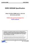
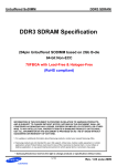
DDR3 SDRAM
Registered DIMM
DDR3 SDRAM Specification
240pin Registered DIMM based on 1Gb E-die
72-bit ECC
78FBGA with Lead-Free
(RoHS compliant)
INFORMATION IN THIS DOCUMENT IS PROVIDED IN RELATION TO SAMSUNG PRODUCTS,
AND IS SUBJECT TO CHANGE WITHOUT NOTICE. NOTHING IN THIS DOCUMENT SHALL BE
CONSTRUED AS GRANTING ANY LICENSE, EXPRESS OR IMPLIED, BY ESTOPPEL OR OTHERWISE, TO ANY INTELLECTUAL PROPERTY RIGHTS IN SAMSUNG PRODUCTS OR TECHNOLOGY. ALL INFORMATION IN THIS DOCUMENT IS PROVIDED ON AS "AS IS" BASIS WITHOUT
GUARANTEE OR WARRANTY OF ANY KIND.
1. For updates or additional information about Samsung products, contact your nearest Samsung office.
2. Samsung products are not intended for use in life support, critical care, medical, safety equipment, or similar
applications where Product failure could result in loss of life or personal or physical harm, or any military or
defense application, or any governmental procurement to which special terms or provisions may apply.
* Samsung Electronics reserves the right to change products or specification without notice.
1 of 53
Rev. 1.06 July 2009
DDR3 SDRAM
Registered DIMM
Table Contents
1.0 DDR3 Registered DIMM Ordering Information .......................................................................... 5
2.0 Key Features ................................................................................................................................ 5
3.0 Address Configuration ................................................................................................................ 5
4.0 Registered DIMM Pin Configurations (Front side/Back side) .................................................. 6
5.0 Pin Description ............................................................................................................................ 7
6.0 ON DIMM Thermal Sensor ........................................................................................................... 7
7.0 Input/Output Functional Description ......................................................................................... 8
8.0 Pinout comparison Based on Module Type .............................................................................. 9
9.0 Registering Clock Driver Specification ................................................................................... 10
9.1 Timing & Capacitance values ...................................................................................................... 10
9.2 Clock driver Characteristics ....................................................................................................... 10
10.0 Functional Block Diagram: ..................................................................................................... 11
10.1 1GB, 128Mx72 Module (Populated as 1 rank of x8 DDR3 SDRAMs) ................................................ 11
10.2 2GB, 256Mx72 Module (Populated as 2 ranks of x8 DDR3 SDRAMs) ............................................... 12
10.3 2GB, 256MX72 module (Populated as 1 rank of x4 DDR3 SDRAMs) ................................................ 13
10.4 4GB, 512Mx72 Module (Populated as 2 ranks of x4 DDR3 SDRAMs) ............................................... 14
10.5 4GB, 512Mx72 Module (Populated as 4 ranks of x8 DDR3 SDRAMs) ............................................... 16
10.6 8GB, 1Gx72 Module (Populated as 4 ranks of x4 DDR3 SDRAMs) .................................................. 17
11.0 Absolute Maximum Ratings .................................................................................................... 22
11.1 Absolute Maximum DC Ratings ................................................................................................. 22
11.2 DRAM Component Operating Temperature Range ....................................................................... 22
12.0 AC & DC Operating Conditions .............................................................................................. 22
12.1 Recommended DC Operating Conditions (SSTL - 15) ................................................................... 22
13.0 AC & DC Input Measurement Levels ...................................................................................... 23
13.1 AC & DC Logic Input Levels for Single-ended Signals .................................................................. 23
13.2 VREF Tolerances ...................................................................................................................... 24
13.3 AC and DC Logic Input Levels for Differential Signals .................................................................. 25
13.3.1 Differential Signals Definition ............................................................................................. 25
13.3.2 Differential Swing Requirement for Clock (CK - CK) and Strobe (DQS - DQS) ........................... 25
13.3.3 Single-ended Requirements for Differential Signals .............................................................. 26
13.3.4 Differential Input Cross Point Voltage .................................................................................. 27
13.4 Slew Rate Definition for Single Ended Input Signals .................................................................... 27
13.5 Slew Rate Definition for Differential Input Signals ........................................................................ 27
14.0 AC and DC Output Measurement Levels ............................................................................... 28
14.1 Single Ended AC and DC Output Levels ..................................................................................... 28
14.2 Differential AC and DC Output Levels ......................................................................................... 28
2 of 53
Rev. 1.06 July 2009
DDR3 SDRAM
Registered DIMM
................................................................................................. 28
14.4 Differential Output Slew Rate .................................................................................................... 29
14.3 Single Ended Output Slew Rate
15.0 IDD specification definition .................................................................................................... 30
15.1 IDD SPEC Table ....................................................................................................................... 32
16.0 Input/Output Capacitance ....................................................................................................... 35
17.0 Electrical Characteristics and AC timing .............................................................................. 36
17.1 Refresh Parameters by Device Density ....................................................................................... 36
17.2 Speed Bins and CL, tRCD, tRC and tRAS for Corresponding Bin ................................................... 36
17.3 Speed Bins and CL, tRCD, tRP, tRC and tRAS for corresponding Bin ............................................. 37
17.3.1 Speed Bin Table Notes ...................................................................................................... 38
18.0 Timing Parameters for DDR3-800, DDR3-1066 and DDR3-1333 .......................................... 39
18.1 Jitter Notes ............................................................................................................................. 42
18.2 Timing Parameter Notes ........................................................................................................... 43
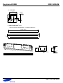
19.0 Physical Dimensions : ............................................................................................................. 44
19.1 128Mbx8 based 128Mx72 Module(1 Rank) - M393B2873EH1 ........................................................... 44
19.1.1 x72 DIMM, populated as one physical rank of x8 DDR3 SDRAMs ............................................ 44
19.2 128Mbx8 based 256Mx72 Module(2 Ranks) - M393B5673EH1 ......................................................... 45
19.2.1 x72 DIMM, populated as two physical ranks of x8 DDR3 SDRAMs ........................................... 45
19.3 256Mbx4 based 256Mx72 Module(1 Rank) - M393B5670EH1 ........................................................... 46
19.3.1 x72 DIMM, populated as one physical rank of x4 DDR3 SDRAMs ............................................ 46
19.4 256Mbx4 based 512Mx72 Module(2 Ranks) - M393B5170EH1 ......................................................... 47
19.4.1 x72 DIMM, populated as two physical ranks of x4 DDR3 SDRAMs ........................................... 47
19.4.2 Heat Spreader Design Guide .............................................................................................. 48
19.5 128Mbx8 based 512Mx72 Module(4 Ranks) M393B5173EH1 ........................................................... 50
19.5.1 x72 DIMM, populated as four physical ranks of x8 DDR3 SDRAMs .......................................... 50
19.6 512Mbx4 based 1Gx72 Module(4 Ranks) M393B1G70EM1.............................................................. 51
19.6.1 x72 DIMM, populated as four physical ranks of x4 DDR3 SDRAMs .......................................... 51
19.6.2 Heat Spreader Design Guide .............................................................................................. 52
3 of 53
Rev. 1.06 July 2009
DDR3 SDRAM
Registered DIMM
Revision History
Revision
Month
Year
History
1.0
December
2008
- First Release
1.01
January
2009
- Corrected Module Physical Dimensions.
1.02
January
2009
- Corrected Typo
1.03
February
2009
- Added Tolerances to Physical Dimensions
1.04
April
2009
- Corrected Module Physical Dimensions
1.05
July
2009
- Corrected Typo.
1.06
July
2009
- Added part number information on physical dimensions page
4 of 53
Rev. 1.06 July 2009
DDR3 SDRAM
Registered DIMM
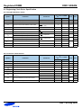
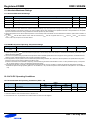
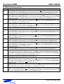
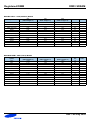
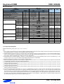
1.0 DDR3 Registered DIMM Ordering Information
Component Composition
Number of
Rank
Height
128Mx72
128Mx8(K4B1G0846E-HC##)*9
1
30mm
256Mx72
128Mx8(K4B1G0846E-HC##)*18
2
30mm
2GB
256Mx72
256Mx4(K4B1G0446E-HC##)*18
1
30mm
4GB
512Mx72
256Mx4(K4B1G0446E-HC##)*36
2
30mm
M393B5173EH1-CF7/F8
4GB
512Mx72
128Mx8(K4B1G0846E-HC##)*36
4
30mm
M393B1G70EM1-CF7/F8
8GB
1Gx72
512Mx4(K4B2G0446E-MC##)*36
4
30mm
Part Number
Density
Organization
M393B2873EH1-CF8/H9
1GB
M393B5673EH1-CF8/H9
2GB
M393B5670EH1-CF8/H9
M393B5170EH1-CF8/H9
* Note
- ## : F7(800Mbps 6-6-6) / F8(1066Mbps 7-7-7) / H9(1333Mbps 9-9-9)
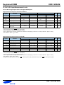
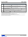
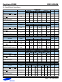
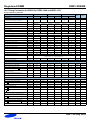
2.0 Key Features
Speed
DDR3-800
DDR3-1066
DDR3-1333
6-6-6
7-7-7
9-9-9
2.5
1.875
1.5
ns
tCK(min)
•
•
•
•
•
•
•
•
•
•
•
•
•
Unit
CAS Latency
6
7
9
tCK
tRCD(min)
15
13.125
13.5
ns
tRP(min)
15
13.125
13.5
ns
tRAS(min)
37.5
37.5
36
ns
tRC(min)
52.5
50.625
49.5
ns
JEDEC standard 1.5V ± 0.075V Power Supply
VDDQ = 1.5V ± 0.075V
400 MHz fCK for 800Mb/sec/pin, 533MHz fCK for 1066Mb/sec/pin, 667MHz fCK for 1333Mb/sec/pin
8 independent internal bank
Programmable CAS Latency: 6,7,8,9,10
Programmable Additive Latency(Posted CAS) : 0, CL - 2, or CL - 1 clock
Programmable CAS Write Latency(CWL) = 5(DDR3-800), 6(DDR3-1066), 7(DDR3-1333)
8-bit pre-fetch
Burst Length: 8 (Interleave without any limit, sequential with starting address “000” only), 4 with tCCD = 4 which does not allow seamless read or
write [either On the fly using A12 or MRS]
Bi-directional Differential Data Strobe
On Die Termination using ODT pin
Average Refresh Period 7.8us at lower then TCASE 85°C, 3.9us at 85°C < TCASE ≤ 95°C
Asynchronous Reset
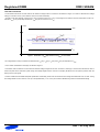
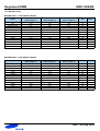
3.0 Address Configuration
Organization
Row Address
Column Address
Bank Address
Auto Precharge
256x4(1Gb) based Module
A0-A13
A0-A9, A11
BA0-BA2
A10/AP
128x8(1Gb) based Module
A0-A13
A0-A9
BA0-BA2
A10/AP
512x4(2Gb DDP) based Module
A0-A13
A0-A9, A11
BA0-BA2
A10/AP
5 of 53
Rev. 1.06 July 2009
DDR3 SDRAM
Registered DIMM
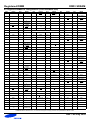
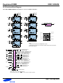
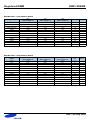
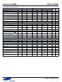
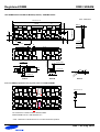
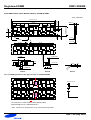
4.0 Registered DIMM Pin Configurations (Front side/Back side)
Pin
Front
Pin
Back
Pin
Front
Pin
Back
Pin
Front
Pin
Back
1
VREFDQ
121
VSS
42
DQS8
162
NC,DQS17
,TDQS17
82
DQ33
202
VSS
2
VSS
122
DQ4
43
DQS8
163
VSS
83
VSS
203
3
DQ0
123
DQ5
44
VSS
164
CB6,NC
84
DQS4
204
4
DQ1
124
VSS
45
CB2,NC
165
CB7,NC
85
DQS4
205
VSS
46
CB3,NC
166
VSS
86
VSS
206
DQ38
47
VSS
167
NC(TEST)
87
DQ34
207
DQ39
48
VTT, NC
168
RESET
88
DQ35
208
VSS
89
VSS
209
DQ44
DM0,DQS9
,TDQS9
NC,DQS9
,TDQS9
5
VSS
125
6
DQS0
126
7
DQS0
127
VSS
8
VSS
128
DQ6
9
DQ2
129
DQ7
50
KEY
49
VTT, NC
DM4,DQS13
,TDQS13
NC,DQS13
,TDQS13
169
CKE1, NC
90
DQ40
210
DQ45
CKE0
170
VDD
91
DQ41
211
VSS
10
DQ3
130
VSS
11
VSS
131
DQ12
51
VDD
171
A15
92
VSS
212
12
DQ8
132
DQ13
52
BA2
172
A14
93
DQS5
213
13
DQ9
133
VSS
53
Err_Out/NC
173
VDD
94
DQS5
214
VSS
54
VDD
174
A12/BC
95
VSS
215
DQ46
55
A11
175
A9
96
DQ42
216
DQ47
DM1,DQS10
,TDQS10
NC,DQS10
,TDQS10
DM5,DQS14
,TDQS14
NC,DQS14
,TDQS14
14
VSS
134
15
DQS1
135
16
DQS1
136
VSS
56
A7
176
VDD
97
DQ43
217
VSS
17
VSS
137
DQ14
57
VDD
177
A8
98
VSS
218
DQ52
18
DQ10
138
DQ15
58
A5
178
A6
99
DQ48
219
DQ53
59
A4
179
VDD
100
DQ49
220
VSS
19
DQ11
139
VSS
20
VSS
140
DQ20
60
VDD
180
A3
101
VSS
221
21
DQ16
141
DQ21
61
A2
181
A1
102
DQS6
222
22
DQ17
142
VSS
62
VDD
182
VDD
103
DQS6
223
VSS
63
NC, CK1
183
VDD
104
VSS
224
DQ54
64
NC, CK1
184
CK0
105
DQ50
225
DQ55
DM2,DQS11
,TDQS11
NC,DQS11
,TDQS11
DM6,DQS15
,TDQS15
NC,DQS15
,TDQS15
23
VSS
143
24
DQS2
144
25
DQS2
145
VSS
65
VDD
185
CK0
106
DQ51
226
VSS
26
VSS
146
DQ22
66
VDD
186
VDD
107
VSS
227
DQ60
27
DQ18
147
DQ23
67
VREFCA
187
EVENT,NC
108
DQ56
228
DQ61
68
NC/Par_In
188
A0
109
DQ57
229
VSS
28
DQ19
148
VSS
29
VSS
149
DQ28
69
VDD
189
VDD
110
VSS
230
30
DQ24
150
DQ29
70
A10/AP
190
BA1
111
DQS7
231
31
DQ25
151
VSS
71
BA0
191
VDD
112
DQS7
232
VSS
72
VDD
192
RAS
113
VSS
233
DQ62
73
WE
193
S0
114
DQ58
234
DQ63
DM3,DQS12
,TDQS12
NC,DQS12
,TDQS12
DM7/DQS16
TDQS16
DM7,DQS16
,TDQS16
32
VSS
152
33
DQS3
153
34
DQS3
154
VSS
74
CAS
194
VDD
115
DQ59
235
VSS
35
VSS
155
DQ30
75
VDD
195
ODT0
116
VSS
236
VDDSPD
36
DQ26
156
DQ31
76
S1,NC
196
A13
117
SA0
237
SA1
37
DQ27
157
VSS
77
ODT1,NC
197
VDD
118
SCL
238
SDA
38
VSS
158
CB4,NC
78
VDD
198
S3,NC
119
SA2
239
VSS
39
CB0,NC
159
CB5,NC
79
S2,NC
199
VSS
120
VTT
240
VTT
40
CB1,NC
160
VSS
80
VSS
200
DQ36
161
DM8,DQS17
TDQS17,NC
81
DQ32
201
DQ37
41
VSS
NC = No Connect
SAMSUNG ELECTRONICS CO., Ltd. reserves the right to change products and specifications without notice.
6 of 53
Rev. 1.06 July 2009
DDR3 SDRAM
Registered DIMM
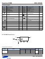
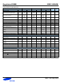
5.0 Pin Description
Pin Name
CK0
Number
Pin Name
Clock Input, positive line
Description
1
ODT[1:0]
Description
Number
On Die Termination Inputs
2
Data Input/Output
64
Data check bits Input/Output
8
Clock Input, negative line
1
DQ[63:0]
Clock Enables
2
CB[7:0]
RAS
Row Address Strobe
1
DQS[8:0]
Data strobes
9
CAS
Column Address Strobe
1
DQS[8:0]
Data strobes, negative line
9
WE
Write Enable
1
DM[8:0]/
DQS[17:9]
TDQS[17:9]
Data Masks/ Data strobes,
Termination data strobes
9
S[3:0]
Chip Selects
4
DQS[17:9]
TDQS[17:9]
Data strobes, negative line, Termination data
strobes
9
2\14
RFU
Reserved for Future Use
2
CK0
CKE[1:0]
A[9:0],A11,
A[15:13]
Address Inputs
A10/AP
Address Input/Autoprecharge
1
EVENT
Reserved for optional hardware temperature
sensing
1
A12/BC
Address Input/Burst chop
1
TEST
Memory bus test toll (Not Connected and Not
Usable on DIMMs)
1
BA[2:0]
SDRAM Bank Addresses
3
RESET
Register and SDRAM control pin
1
SCL
Serial Presence Detect (SPD) Clock Input
1
VDD
Power Supply
22
SDA
SPD Data Input/Output
1
VSS
Ground
59
SPD Address Inputs
3
VREFDQ
Reference Voltage for DQ
1
Reference Voltage for CA
1
Termination Voltage
4
SA[2:0]
Par_In
Parity bit for the Address and Control bus
1
VREFCA
Err_Out
Parity error found on the Address and Control
bus
1
VTT
VDDSPD
SPD Power
1
Total
240
*The VDD and VDDQ pins are tied common to a single power-plane on these designs.
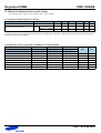
6.0 ON DIMM Thermal Sensor
SCL
SDA
EVENT
WP/EVENT
R1
0Ω
R2
0Ω
SA0
SA1
SA2
SA0
SA1
SA2
Temperature Sensor Characteristics
Grade
Range
B
-20 < Ta < 125
Temperature Sensor Accuracy
Min.
Typ.
Max.
75 < Ta < 95
-
+/- 0.5
+/- 1.0
40 < Ta < 125
-
+/- 1.0
+/- 2.0
-
+/- 2.0
+/- 3.0
Resolution
0.25
7 of 53
Units
Notes
-
°C
-
°C /LSB
-
-
Rev. 1.06 July 2009
DDR3 SDRAM
Registered DIMM
7.0 Input/Output Functional Description
Symbol
Type
Polarity
Function
CK0
Input
Positive
Edge
CK0
Input
Negative
Negative line of the differential pair of system clock inputs that drives the input to the on-DIMM Clock Driver.
Edge
CKE[1:0]
Input
CKE HIGH activates, and CKE LOW deactivates internal clock signals, and device input buffers
Active High and output drivers of the SDRAMs. Taking CKE LOW provides PRECHARGE POWER-DOWN
and SELF REFRESH operation (all banks idle), or ACTIVE POWER DOWN (row ACTIVE in any bank)
S[3:0]
Input
Enables the associated SDRAM command decoder when low and disables decoder when high.
When decoder is disabled, new commands are ignored and previous operations continue.
These input signals also disable all outputs (except CKE and ODT) of the register(s) on the DIMM when both
Active Low
inputs are high. When both S[1:0] are high, all register outputs (except CKE, ODT and Chip select) remain in
the previous state. For modules supporting 4 ranks, S[3:2] operate similarly to S[1:0] for a second set of register outputs.
ODT[1:0]
Input
Active High On-Die Termination control signals
RAS, CAS, WE
Input
Active Low
VREFDQ
Supply
VREFCA
Supply
Positive line of the differential pair of system clock inputs that drives input to the on-DIMM Clock Driver.
When sampled at the positive rising edge of the clock, CAS, RAS, and WE define the operation to be executed by the SDRAM.
Reference voltage for DQ0-DQ63 and CB0-CB7
Reference voltage for A0-A15, BA0-BA2, RAS, CAS, WE, S0, S1, CKE0, CKE1, Par_In, ODT0 and ODT1.
Input
Selects which SDRAM bank of eight is activated.
BA0 - BA2 define to which bank an Active, Read, Write or Precharge command is being applied. Bank
address also determines mode register is to be accessed during an MRS cycle.
A[15:13,
12/BC,11,
10/AP,9:0]
Input
Provided the row address for Active commands and the column address and Auto Precharge bit for Read/
Write commands to select one location out of the memory array in the respective bank. A10 is sampled during a Precharge command to determine whether the Precharge applies to one bank (A10 LOW) or all banks
(A10 HIGH). If only one bank is to be precharged, the bank is selected by BA. A12 is also utilized for BL 4/8
identification for "BL on the fly" during CAS command. The address inputs also provide the op-code during
Mode Register Set commands.
DQ[63:0],
CB[7:0]
I/O
BA[2:0]
Data and Check Bit Input/Output pins
Active High Masks write data when high, issued concurrently with input data.
VDD, VSS Supply Power and ground for the DDR SDRAM input buffers and core logic.
VTT Supply Termination Voltage for Address/Command/Control/Clock nets.
DM[8:0]
DQS[17:0]
I/O
Positive Edge Positive line of the differential data strobe for input and output data.
DQS[17:0]
I/O
Negative Edge Negative line of the differential data strobe for input and output data.
TDQS[17:9],
TDQS[17:9]
OUT
SA[2:0]
IN
These signals are tied at the system planar to either VSS or VDDSPD to configure the serial SPD EEPROM
address range.
SDA
I/O
This bidirectional pin is used to transfer data into or out of the SPD EEPROM. A resistor must be
connected from the SDA bus line to VDDSPD on the system planar to act as a pull-up.
SCL
IN
This signal is used to clock data into and out of the SPD EEPROM. A resistor may be connected
from the SCL bus time to VDDSPD on the system planar to act as a pull-up.
EVENT
OUT
(open
drain)
VDDSPD
Supply
Serial EEPROM positive power supply wired to a separate power pin at the connector which supports from
3.0 Volt to 3.6 Volt (nominal 3.3V) operation.
RESET
IN
The RESET pin is connected to the RESET pin on the register and to the RESET pin on the DRAM. When
low, all register outputs will be driven low and the Clock Driver clocks to the DRAMs and register(s) will be set
to low level (the Clock Driver will remain synchronized with the input clock)
Par_In
IN
Parity bit for the Address and Control bus. ("1 " : Odd, "0 ": Even)
Err_Out
OUT
(open
drain)
TEST
TDQS/TDQS is applicable for X8 DRAMs only. When enabled via Mode Register A11=1 in MR1, DRAM will
enable the same termination resistance function on TDQS/TDQS that is applied to DQS/DQS. When disabled via mode register A11=0 in MR1, DM/TDQS will provide the data mask function and TDQS is not used.
X4/X16 DRAMs must disable the TDQS function via mode register A11=0 in MR1
Active Low
This signal indicates that a thermal event has been detected in the thermal sensing device.The system
should guarantee the electrical level requirement is met for the EVENT pin on TS/SPD part.
Parity error detected on the Address and Control bus. A resistor may be connected from Err_Out
bus line to VDD on the system planar to act as a pull up.
Used by memory bus analysis tools (unused (NC) on memory DIMMs)
8 of 53
Rev. 1.06 July 2009
DDR3 SDRAM
Registered DIMM
8.0 Pinout comparison Based on Module Type
Pin
RDIMM
UDIMM
Signal
Notes
Signal
48, 49
VTT
Additional connection for Termination Voltage for
Address/Command/Control/Clock nets.
NC
Not used on UDIMMs
120, 240
VTT
Termination Voltage for Address/Command/Control/Clock nets.
VTT
Termination Voltage for Address/Command/Control/Clock nets.
53
Err_Out
Connected to the register on all RDIMMs NC Not
used on UDIMMs
NC
NC Not used on UDIMMs
63
NC
CK1
64
NC
CK1
Used for 2 rank UDIMMs, not used on single-rank
UDIMMs, but terminated
68
Par_In
Connected to the register on all RDIMMs
NC
Not used on RDIMMs
76
S1
Connected to the register on all RDIMMs
S1
Used for dual-rank UDIMMs, not connected
on single-rank UDIMMs
77
ODT1, NC
ODT1,NC
Used for dual-rank UDIMMs, not connected
on single-rank UDIMMs
79
S2, NC
Connected to the register on quad-rank
RDIMMs, not connected on single or dual rank
RDIMMs
NC
Not used on UDIMMs
167
NC
TEST input used only on bus analysis probes
NC
TEST input used only on bus analysis
probes
169
CKE1
171
A15
172
A14
196
A13
198
S3, NC
39, 40, 45, 46,
158, 159, 164,
165
CBn
125, 134, 143,
152, 161, 203,
212, 221, 230
DQSn,
TDQSn
Connected to DQS on x4 SDRAMs,
TDQS on x8 SDRAMs on RDIMMs; (n = 9...17)
DMn
126, 135, 144,
153, 162, 204,
213, 222, 231
DQSn,
TDQSn
Connected to DQS on x4 DRAMs, TDQS on x8
SDRAMs on RDIMMs; (n=9...17)
NC
Not used on UDIMMs
187
EVENT
NC
Connected to optional thermal sensing component.
NC on Modules without a thermal sensing
component.
NC
Not used on UDIMMs
Not used on RDIMMs
Connected to the register on dual- and quadrank
RDIMMs; NC on single-rank RDIMMs
Connected to the register on dual- and quadrank
RDIMMs; NC on single-rank RDIMMs
CKE1,
NC
A15, NC
Connected to the register on all RDIMMs
Connected to the register on quad-rank
RDIMMs, not connected on single-or dual-rank
RDIMMs
Used on all RDIMMs; (n = 0...7)
Notes
Used for dual-rank UDIMMs, not connected
on single-rank UDIMMs
A13
Depending on device density, may not be
connected to SDRAMs on UDIMMs. However,
these signals are terminated on
UDIMMs. A15 not routed on some RCs
NC
Not used on UDIMMs
A14
NC, CBn
Used on x72 UDIMMs, (n = 0...7); not
used on x64 UDIMMs
Connected to DM on x8 DRAMs, UDM or
LDM on x16 DRAMs on UDIMMs;
(n = 0...8)
Note : NC = no internal connection
9 of 53
Rev. 1.06 July 2009
DDR3 SDRAM
Registered DIMM
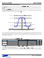
9.0 Registering Clock Driver Specification
9.1 Timing & Capacitance values
Symbol
Parameter
fclock
Input Clock Frequency
tCH/tCL
Pulse duration, CK, CK HIGH or LOW
Conditions
application frequency
TC = TBD
VDD = 1.5 ± 0.075V
Min
Max
300
670
MHz
0.4
-
tCK
8
-
tCK
ps
tACT
Inputs active time4 before RESET is taken HIGH
DCKE0/1 = LOW and
DCS0/1 = HIGH
tSU
Setup time
Input valid before CK/CK
100
-
tH
Hold time
Input to remain Valid after CK/
CK
175
-
Propagation delay, single-bit switching
CK/CK to output
0.65
1.0
tPDM
tDIS
tEN
output disable time(1/2-Clock pre-launch)
output disable time(3/4-Clock pre-launch)
output enable time(1/2-Clock pre-launch)
output enable time(3/4-Clock pre-launch)
CK/CK to output float
CK/CK to output driving
Units Notes
0.5
-
0.25
-
-
0.5
-
0.25
CIN(DATA)
Data Input Capacitance
1.5
2.5
CIN(CLOCK)
Data Input Capacitance
2
3
CIN(RST)
Reset Input Capacitance
-
3
ns
tCK
tCK
pF
9.2 Clock driver Characteristics
Symbol
Parameter
Conditions
TC = TBD
VDD = 1.5 ± 0.075V
Min
Max
Units Notes
tjit (cc)
Cycle-to-cycle period jitter
0
40
ps
tSTAB
Stabilization time
-
6
us
tfdyn
Dynamic phase offset
-50
50
ps
tCKsk
50
ps
tjit(per)
Yn Clock Period jitter
Clock Output skew
-40
40
ps
tjit(hper)
Half period jitter
-50
50
ps
Output Inversion enabled
-100
200
OUtput Inversion disabled
-100
300
Output Inversion enabled
-100
200
OUtput Inversion disabled
-100
300
-80
80
tQsk1
Qn Output to clock tolerance (Standard 1/2 -Clcok
Pre-Launch)
tQsk1
Output clock tolerance (3/4 Clock Pre-Launch)
tdynoff
Maximum re-driven dynamic clock off-set
10 of 53
ps
ps
ps
Rev. 1.06 July 2009
DDR3 SDRAM
Registered DIMM
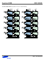
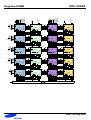
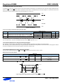
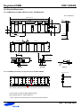
10.0 Functional Block Diagram:
DQS0
DQS0
DM0/DQS9
DQS9
DQ[7:0]
CS
RAS
CAS
WE
CK
CK
CKE
ODT
A[N:0]/BA[N:0]
CS
RAS
CAS
WE
CK
CK
CKE
ODT
A[N:0]/BA[N:0]
ZQ
DQS
DQS
TDQS
TDQS
DQ[7:0]
D2
ZQ
CS
RAS
CAS
WE
CK
CK
CKE
ODT
A[N:0]/BA[N:0]
DQS1
DQS1
DM1/DQS10
DQS10
DQ[15:8]
DQS
DQS
TDQS
TDQS
DQ[7:0]
D3
DQS
DQS
TDQS
TDQS
DQ[7:0]
D1
DQS
DQS
TDQS
TDQS
DQ[7:0]
DQS6
DQS6
DM6/DQS15
DQS15
DQ[55:48]
DQS7
DQS7
DM7/DQS16
DQS16
DQ[63:56]
ZQ
D0
Vtt
S0*
S1*
BA[N:0]
A[N:0]
1:2
R
E
G
I
S
T
E
R
RAS
CAS
WE
CKE0
ODT0
CK0
CK0
PAR_IN
QERR
RESET**
ZQ
CS
RAS
CAS
WE
CK
CK
CKE
ODT
A[N:0]/BA[N:0]
DQS5
DQS5
DM5/DQS14
DQS14
DQ[47:40]
CS
RAS
CAS
WE
CK
CK
CKE
ODT
A[N:0]/BA[N:0]
DQS2
DQS2
DM2/DQS11
DQS11
DQ[23:16]
ZQ
DQS
DQS
TDQS
TDQS
DQ[7:0]
D4
DQS
DQS
TDQS
TDQS
DQ[7:0]
DQS
DQS
TDQS
TDQS
DQ[7:0]
Thermal sensor with SPD
ZQ
CS
RAS
CAS
WE
CK
CK
CKE
ODT
A[N:0]/BA[N:0]
DQS
DQS
TDQS
TDQS
DQ[7:0]
D8
DQS4
DQS4
DM4/DQS13
DQS13
DQ[39:32]
D5
SCL
EVENT
EVENT
A0
SDA
A1
A2
SA0 SA1 SA2
ZQ
CS
RAS
CAS
WE
CK
CK
CKE
ODT
A[N:0]/BA[N:0]
DQS3
DQS3
DM3/DQS12
DQS12
DQ[31:24]
ZQ
D6
ZQ
CS
RAS
CAS
WE
CK
CK
CKE
ODT
A[N:0]/BA[N:0]
DQS
DQS
TDQS
TDQS
DQ[7:0]
CS
RAS
CAS
WE
CK
CK
CKE
ODT
A[N:0]/BA[N:0]
DQS8
DQS8
DM8/DQS17
DQS17
CB[7:0]
RS0B
RRASB
RCASB
RWEB
PCK0B
PCK0B
RCLE0B
RODT0B
A[N:0]B
/BA[N:0]B
RS0A
RRASA
RCASA
RWEA
PCK0A
PCK0A
RCLE0A
RODT0A
A[N:0]A
/BA[N:0]A
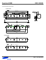
10.1 1GB, 128Mx72 Module (Populated as 1 rank of x8 DDR3 SDRAMs)
D7
Vtt
VDDSPD
Serial PD
VDD
D0 - D8
VTT
VREFCA
D0 - D8
VREFDQ
D0 - D8
VSS
D0 - D8
Note :
1. DQ-to-I/O wiring may be changed within a byte.
2. ZQ resistors are 240 1% For all other resistor values refer to the appropriate wiring diagram.
RS0A-> CS0 : SDRAMs D[3:0], D8
RS0B-> CS0 : SDRAMs D[7:4]
RBA[N:0]A -> BA[N:0] : SDRAMs D[3:0], D8
RBA[N:0]B -> BA[N:0] : SDRAMs D[7:4]
RA[N:0]A -> A[N:0] : SDRAMs D[3:0], D8
RA[N:0]B -> A[N:0] : SDRAMs D[7:4]
RRASA -> RAS : SDRAMs D[3:0], D8
RRASB -> RAS : SDRAMs D[7:4]
RCASA -> CAS : SDRAMs D[3:0], D8
RCASB -> CAS : SDRAMs D[7:4]
RWEA -> WE : SDRAMs D[3:0], D8
RWEB -> WE : SDRAMs D[7:4]
RCKE0A -> CKE0 : SDRAMs D[3:0], D8
RCKE0B -> CKE0 : SDRAMs D[7:4]
RODT0A -> ODT0 : SDRAMs D[3:0], D8
RODT0B -> ODT0 : SDRAMs D[7:4]
PCK0A -> CK : SDRAMs D[3:0], D8
PCK0A -> CK : SDRAMs D[7:4]
PCK0A -> CK : SDRAMs D[3:0], D8
PCK0A -> CK : SDRAMs D[7:4]
Err_out
RST
PST** : SDRAMs D[8:0]
*S[3:2], CKE1, ODT1, CK1 and CK1 are NC
(Unused register inputs ODT1 and CKE1 have a 330 ohm resistor to ground)
11 of 53
Rev. 1.06 July 2009
DDR3 SDRAM
Registered DIMM
DQS7
DQS7
DM7/DQS16
DQS16
DQ[63:56]
DQS
DQS
TDQS
TDQS
DQ[7:0]
ZQ
D7
D14
DQS
DQS
TDQS
TDQS
DQ[7:0]
ZQ
D15
DQS
DQS
TDQS
TDQS
DQ[7:0]
ZQ
D16
CS
RAS
CAS
WE
CK
CK
CKE
ODT
A[N:0]/BA[N:0]
D5
Vtt
D9
S0*
RS0A-> CS0 : SDRAMs D[3:0], D8
RS0B-> CS0 : SDRAMs D[7:4]
RS1A-> CS1 : SDRAMs D[12:9], D17
RS1B-> CS1 : SDRAMs D[16:13]
RBA[N:0]A -> BA[N:0] : SDRAMs D[3:0], D[12:8], D17
RBA[N:0]B -> BA[N:0] : SDRAMs D[7:4], D[16:13]
RA[N:0]A -> A[N:0] : SDRAMs D[3:0], D[12:8], D17
RA[N:0]B -> A[N:0] : SDRAMs D[7:4, D[16:13]]
S1*
BA[N:0]
Vtt
A[N:0]
RAS
VDDSPD
Serial PD
VDD
D0 - D17
VTT
Thermal sensor with SPD
CAS
SCL
EVENT
PCK1B
PCK1B
RCKE1B
RODT1B
DQS
DQS
TDQS
TDQS
DQ[7:0]
ZQ
CS
RAS
CAS
WE
CK
CK
CKE
ODT
A[N:0]/BA[N:0]
D6
RS1B
RS0B
RRASB
RCASB
RWEB
PCK0B
PCK0B
RCKE0B
RODT0B
A[N:0]B
/BA[N:0]B
RS1A
PCK1A
PCK1A
RCKE1A
RODT1A
DQS
DQS
TDQS
TDQS
DQ[7:0]
ZQ
D13
CS
RAS
CAS
WE
CK
CK
CKE
ODT
A[N:0]/BA[N:0]
CS
RAS
CAS
WE
CK
CK
CKE
ODT
A[N:0]/BA[N:0]
CS
RAS
CAS
WE
CK
CK
CKE
ODT
A[N:0]/BA[N:0]
CS
RAS
CAS
WE
CK
CK
CKE
ODT
A[N:0]/BA[N:0]
CS
RAS
CAS
WE
CK
CK
CKE
ODT
A[N:0]/BA[N:0]
D0
DQS
DQS
TDQS
TDQS
DQ[7:0]
ZQ
DQS6
DQS6
DM6/DQS15
DQS15
DQ[55:48]
DQS
DQS
TDQS
TDQS
DQ[7:0]
ZQ
CS
RAS
CAS
WE
CK
CK
CKE
ODT
A[N:0]/BA[N:0]
DQS
DQS
TDQS
TDQS
DQ[7:0]
ZQ
D10
DQS
DQS
TDQS
TDQS
DQ[7:0]
ZQ
CS
RAS
CAS
WE
CK
CK
CKE
ODT
A[N:0]/BA[N:0]
DQS0
DQS0
DM0/DQS9
DQS9
DQ[7:0]
D1
DQS
DQS
TDQS
TDQS
DQ[7:0]
ZQ
DQS5
DQS5
DM5/DQS14
DQS14
DQ[47:40]
D4
CS
RAS
CAS
WE
CK
CK
CKE
ODT
A[N:0]/BA[N:0]
DQS
DQS
TDQS
TDQS
DQ[7:0]
ZQ
D11
DQS
DQS
TDQS
TDQS
DQ[7:0]
ZQ
CS
RAS
CAS
WE
CK
CK
CKE
ODT
A[N:0]/BA[N:0]
DQS1
DQS1
DM1/DQS10
DQS10
DQ[15:8]
D2
DQS
DQS
TDQS
TDQS
DQ[7:0]
ZQ
D12
DQS4
DQS4
DM4/DQS13
DQS13
DQ[39:32]
CS
RAS
CAS
WE
CK
CK
CKE
ODT
A[N:0]/BA[N:0]
DQS
DQS
TDQS
TDQS
DQ[7:0]
ZQ
CS
RAS
CAS
WE
CK
CK
CKE
ODT
A[N:0]/BA[N:0]
DQS2
DQS2
DM2/DQS11
DQS11
DQ[23:16]
D3
DQS
DQS
TDQS
TDQS
DQ[7:0]
ZQ
CS
RAS
CAS
WE
CK
CK
CKE
ODT
A[N:0]/BA[N:0]
DQS
DQS
TDQS
TDQS
DQ[7:0]
ZQ
D17
CS
RAS
CAS
WE
CK
CK
CKE
ODT
A[N:0]/BA[N:0]
DQS3
DQS3
DM3/DQS12
DQS12
DQ[31:24]
D8
DQS
DQS
TDQS
TDQS
DQ[7:0]
ZQ
CS
RAS
CAS
WE
CK
CK
CKE
ODT
A[N:0]/BA[N:0]
DQS
DQS
TDQS
TDQS
DQ[7:0]
ZQ
CS
RAS
CAS
WE
CK
CK
CKE
ODT
A[N:0]/BA[N:0]
DQS8
DQS8
DM8/DQS17
DQS17
CB[7:0]
CS
RAS
CAS
WE
CK
CK
CKE
ODT
A[N:0]/BA[N:0]
RS0A
RRASA
RCASA
RWEA
PCK0A
PCK0A
RCKE0A
RODT0A
A[N:0]A
/BA[N:0]A
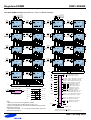
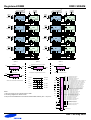
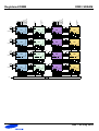
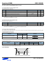
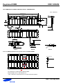
10.2 2GB, 256Mx72 Module (Populated as 2 ranks of x8 DDR3 SDRAMs)
EVENT
A0
SDA
A1
A2
1:2
R
E
G
I
S
T
E
R
WE
CKE0
SA0 SA1 SA2
VREFCA
D0 - D17
VREFDQ
D0 - D17
ODT0
VSS
D0 - D17
ODT1
CKE1
Note :
1. DQ-to-I/O wiring may be changed within a byte.
2. Unless otherwise noted, resistor values are 15Ω ± 5%.
3. RS0 and RS1 alternate between the back and front sides of the
DIMM.
4. ZQ resistors are 240Ω ± 1% . For all other resistor values refer to the
appropriate wiring diagram.
5. See the wiring diagrams for all resistors associated with the command,
address and control bus.
12 of 53
RRASA -> RAS : SDRAMs D[3:0], D[12:8], D17
RRASB -> RAS : SDRAMs D[7:4], D[16:13]
RCASA -> CAS : SDRAMs D[3:0], D[12:8], D17
RCASB -> CAS : SDRAMs D[7:4], D[16:13]
RWEA -> WE : SDRAMs D[3:0], D[12:8], D17
RWEB -> WE : SDRAMs D[7:4], D[16:13]
RCKE0A -> CKE0 : SDRAMs D[3:0], D8
RCKE0B -> CKE0 : SDRAMs D[7:4]
RCKE1A -> CKE1 : SDRAMs D[12:9], D17
RCKE1B -> CKE1 : SDRAMs D[16:13]
RODT0A -> ODT0 : SDRAMs D[3:0], D8
RODT0B -> ODT0 : SDRAMs D[7:4]
RODT1A -> ODT1 : SDRAMs D[12:9], D17
RODT1A -> ODT1 : SDRAMs D[16:13]
CK0
PCK0A -> CK : SDRAMs D[3:0], D8
PCK0B -> CK : SDRAMs D[7:4]
PCK1A -> CK : SDRAMs D[12:9], D17
PCK1B -> CK : SDRAMs D[16:13]
CK0
PCK0A -> CK : SDRAMs D[3:0], D8
PCK0B -> CK : SDRAMs D[7:4]
PCK1A -> CK : SDRAMs D[12:9], D17
PCK1B -> CK : SDRAMs D[16:13]
QERR
PAR_IN
RESET**
Err_out
RST
PST** : SDRAMs D[8:0]
*S[3:2], CKE1, ODT1, CK1 and CK1 are NC
Rev. 1.06 July 2009
DDR3 SDRAM
Registered DIMM
CS
RAS
CAS
WE
CK
CK
CKE
ODT
A[N:0]/BA[N:0]
D0
ZQ
D9
D7
S0*
SDA
A2
SA0 SA1 SA2
VSS
CS
RAS
CAS
WE
CK
CK
CKE
ODT
A[N:0]/BA[N:0]
VSS
CS
RAS
CAS
WE
CK
CK
CKE
ODT
A[N:0]/BA[N:0]
D15
VSS
DQS
DQS
DM
DQ[3:0]
ZQ
ZQ
D16
RS0A-> CS0 : SDRAMs D[3:0], D[12:8], D17
RS0B-> CS0 : SDRAMs D[7:4], D[16:13]]
S1*
RBA[N:0]A -> BA[N:0] : SDRAMs D[3:0], D[12:8], D17
RBA[N:0]B -> BA[N:0] : SDRAMs D[7:4], D[16:13]
RA[N:0]A -> A[N:0] : SDRAMs D[3:0], D[12:8], D17
RA[N:0]B -> A[N:0] : SDRAMs D[7:4], D[16:13]
CAS
A1
DQS17
DQS17
VSS
DQ[63:60]
ZQ
D14
VSS
D6
RAS
EVENT
A0
DQS
DQS
DM
DQ[3:0]
ZQ
Vtt
Vtt
SCL
DQS17
DQS17
VSS
DQ[55:52]
ZQ
A[N:0]
EVENT
DQS
DQS
DM
DQ[3:0]
D13
CS
RAS
CAS
WE
CK
CK
CKE
ODT
A[N:0]/BA[N:0]
CS
RAS
CAS
WE
CK
CK
CKE
ODT
A[N:0]/BA[N:0]
D5
BA[N:0]
Thermal sensor with SPD
DQS17
DQS17
VSS
DQ[47:44]
ZQ
ZQ
CS
RAS
CAS
WE
CK
CK
CKE
ODT
A[N:0]/BA[N:0]
D10
VSS
DQS
DQS
DM
DQ[3:0]
VSS
DQS8
DQS8
VSS
DQ[59:56]
ZQ
DQS
DQS
DM
DQ[3:0]
VSS
D11
DQS17
DQS17
VSS
DQ[39:36]
VSS
DQS
DQS
DM
DQ[3:0]
CS
RAS
CAS
WE
CK
CK
CKE
ODT
A[N:0]/BA[N:0]
DQS8
DQS8
VSS
DQ[51:48]
ZQ
D4
CS
RAS
CAS
WE
CK
CK
CKE
ODT
A[N:0]/BA[N:0]
DQS
DQS
DM
DQ[3:0]
D12
ZQ
CS
RAS
CAS
WE
CK
CK
CKE
ODT
A[N:0]/BA[N:0]
DQS17
DQS17
VSS
DQ[7:4]
ZQ
VSS
CS
RAS
CAS
WE
CK
CK
CKE
ODT
A[N:0]/BA[N:0]
D1
VSS
DQS
DQS
DM
DQ[3:0]
DQS
DQS
DM
DQ[3:0]
VSS
DQS17
DQS17
VSS
DQ[15:12]
ZQ
DQS8
DQS8
VSS
DQ[43:40]
VSS
CS
RAS
CAS
WE
CK
CK
CKE
ODT
A[N:0]/BA[N:0]
CS
RAS
CAS
WE
CK
CK
CKE
ODT
A[N:0]/BA[N:0]
D2
DQS
DQS
DM
DQ[3:0]
VSS
DQS
DQS
DM
DQ[3:0]
CS
RAS
CAS
WE
CK
CK
CKE
ODT
A[N:0]/BA[N:0]
DQS17
DQS17
VSS
DQ[23:20]
ZQ
CS
RAS
CAS
WE
CK
CK
CKE
ODT
A[N:0]/BA[N:0]
DQS
DQS
DM
DQ[3:0]
D3
DQS8
DQS8
VSS
DQ[35:32]
ZQ
CS
RAS
CAS
WE
CK
CK
CKE
ODT
A[N:0]/BA[N:0]
DQS8
DQS8
VSS
DQ[3:0]
DQS
DQS
DM
DQ[3:0]
D17
CS
RAS
CAS
WE
CK
CK
CKE
ODT
A[N:0]/BA[N:0]
DQS
DQS
DM
DQ[3:0]
DQS17
DQS17
VSS
DQ[31:28]
ZQ
ZQ
CS
RAS
CAS
WE
CK
CK
CKE
ODT
A[N:0]/BA[N:0]
DQS8
DQS8
VSS
DQ[11:8]
VSS
DQS
DQS
DM
DQ[3:0]
VSS
DQS8
DQS8
VSS
DQ[19:16]
DQS
DQS
DM
DQ[3:0]
VSS
DQS
DQS
DM
DQ[3:0]
D8
DQS17
DQS17
VSS
CB[7:4]
VSS
DQS3
DQS3
VSS
DQ[27:24]
ZQ
VSS
DQS
DQS
DM
DQ[3:0]
CS
RAS
CAS
WE
CK
CK
CKE
ODT
A[N:0]/BA[N:0]
DQS8
DQS8
VSS
CB[3:0]
RS0B
RRASB
RCASB
RWEB
PCK0B
PCK0B
RCKE0B
RODT0B
A[N:0]B
/BA[N:0]B
RS0A
RRASA
RCASA
RWEA
PCK0A
PCK0A
RCKE0A
RODT0A
A[N:0]A
/BA[N:0]A
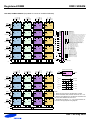
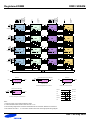
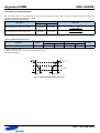
10.3 2GB, 256Mx72 module (Populated as 1 rank of x4 DDR3 SDRAMs)
VDDSPD
Serial PD
WE
VDD
D0 - D17
CKE0
VTT
1:2
R
E
G
I
S
T
E
R
ODT0
VREFCA
D0 - D17
VREFDQ
D0 - D17
VSS
D0 - D17
Note :
1. DQ-to-I/O wiring may be changed within a nibble.
2. Unless otherwise noted, resistor values are 15Ω ± 5%.
3. See the wiring diagrams for all resistors associated with the command,
address and control bus.
4. ZQ resistors are 240Ω ± 1% . For all other resistor values refer to the
appropriate wiring diagram.
13 of 53
RRASA -> RAS : SDRAMs D[3:0], D[12:8], D17
RRASB -> RAS : SDRAMs D[7:4], D[16:13]
RCASA -> CAS : SDRAMs D[3:0], D[12:8], D17
RCASB -> CAS : SDRAMs D[7:4], D[16:13]
RWEA -> WE : SDRAMs D[3:0], D[12:8], D17
RWEB -> WE : SDRAMs D[7:4], D[16:13]
RCKE0A -> CKE0 : SDRAMs D[3:0], D[12:8], D17
RCKE0B -> CKE0 : SDRAMs D[7:4], D[16:13]
RODT0A -> ODT0 : SDRAMs D[3:0], D[12:8], D17
RODT0B -> ODT0 : SDRAMs D[7:4], D[16:13]
CK0
PCK0A -> CK : SDRAMs D[3:0], D[12:8], D17
PCK0B -> CK : SDRAMs D[7:4], D[16:13]
CK0
PCK0A -> CK : SDRAMs D[3:0], D[12:8], D17
PCK0B -> CK : SDRAMs D[7:4], D[16:13]
QERR
PAR_IN
RESET**
Err_out
RST
PST** : SDRAMs D[17:0]
*S[3:2], CKE1, ODT1, CK1 and CK1 are NC
(Unused register inputs ODT1 and CKE1 have a 330 Ω resistor to ground)
Rev. 1.06 July 2009
DQS11
DQS11
VSS
DQ[23:20]
DQS
DQS
DM
DQ[3:0]
DQS10
DQS10
VSS
DQ[15:12]
DQS
DQS
DM
DQ[3:0]
DQS0
DQS0
VSS
DQ[3:0]
DQS
DQS
DM
DQ[3:0]
Vtt
D11
D10
D0
CS
RAS
CAS
WE
CK
CK
CKE
ODT
A[N:0]/BA[N:0]
CS
RAS
CAS
WE
CK
CK
CKE
ODT
A[N:0]/BA[N:0]
D12
CS
RAS
CAS
WE
CK
CK
CKE
ODT
A[N:0]/BA[N:0]
CS
RAS
CAS
WE
CK
CK
CKE
ODT
A[N:0]/BA[N:0]
D17
DQS
DQS
DM
DQ[3:0]
CS
RAS
CAS
WE
CK
CK
CKE
ODT
A[N:0]/BA[N:0]
CS
RAS
CAS
WE
CK
CK
CKE
ODT
A[N:0]/BA[N:0]
DQS
DQS
DM
DQ[3:0]
CS
RAS
CAS
WE
CK
CK
CKE
ODT
A[N:0]/BA[N:0]
DQS12
DQS12
VSS
DQ[31:28]
CS
RAS
CAS
WE
CK
CK
CKE
ODT
A[N:0]/BA[N:0]
DQS
DQS
DM
DQ[3:0]
CS
RAS
CAS
WE
CK
CK
CKE
ODT
A[N:0]/BA[N:0]
DQS17
DQS17
VSS
CB[7:4]
CS
RAS
CAS
WE
CK
CK
CKE
ODT
A[N:0]/BA[N:0]
DQS
DQS
DM
DQ[3:0]
DQS
DQS
DM
DQ[3:0]
DQS
DQS
DM
DQ[3:0]
DQS
DQS
DM
DQ[3:0]
D35
D30
D29
D28
D18
DQS11
DQS11
VSS
DQ[19:16]
DQS
DQS
DM
DQ[3:0]
DQS10
DQS10
VSS
DQ[11:8]
DQS
DQS
DM
DQ[3:0]
DQS0
DQS0
VSS
DQ[7:4]
DQS
DQS
DM
DQ[3:0]
14 of 53
D2
D1
D9
CS
RAS
CAS
WE
CK
CK
CKE
ODT
A[N:0]/BA[N:0]
CS
RAS
CAS
WE
CK
CK
CKE
ODT
A[N:0]/BA[N:0]
D3
CS
RAS
CAS
WE
CK
CK
CKE
ODT
A[N:0]/BA[N:0]
CS
RAS
CAS
WE
CK
CK
CKE
ODT
A[N:0]/BA[N:0]
D8
DQS
DQS
DM
DQ[3:0]
CS
RAS
CAS
WE
CK
CK
CKE
ODT
A[N:0]/BA[N:0]
CS
RAS
CAS
WE
CK
CK
CKE
ODT
A[N:0]/BA[N:0]
DQS
DQS
DM
DQ[3:0]
CS
RAS
CAS
WE
CK
CK
CKE
ODT
A[N:0]/BA[N:0]
DQS12
DQS12
VSS
DQ[27:24]
CS
RAS
CAS
WE
CK
CK
CKE
ODT
A[N:0]/BA[N:0]
DQS
DQS
DM
DQ[3:0]
CS
RAS
CAS
WE
CK
CK
CKE
ODT
A[N:0]/BA[N:0]
DQS17
DQS17
VSS
CB[3:0]
CS
RAS
CAS
WE
CK
CK
CKE
ODT
A[N:0]/BA[N:0]
DQS
DQS
DM
DQ[3:0]
DQS
DQS
DM
DQ[3:0]
DQS
DQS
DM
DQ[3:0]
DQS
DQS
DM
DQ[3:0]
PCK1A
PCK1A
RCKE1A
RODT1A
RS1A
RS0A
RRASA
RCASA
RWEA
PCK0A
PCK0A
RCKE0A
RODT0A
A[N:0]A
/BA[N:0]A
PCK1A
PCK1A
RCKE1A
RODT1A
RS1A
RS0A
RRASA
RCASA
RWEA
PCK0A
PCK0A
RCKE0A
RODT0A
A[N:0]A
/BA[N:0]A
Registered DIMM
DDR3 SDRAM
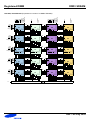
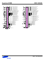
10.4 4GB, 512Mx72 Module (Populated as 2 ranks of x4 DDR3 SDRAMs)
D26
D21
D20
D19
D27
Vtt
Rev. 1.06 July 2009
DQS6
DQS6
VSS
DQ[51:48]
DQS
DQS
DM
DQ[3:0]
Vtt
CS
RAS
CAS
WE
CK
CK
CKE
ODT
A[N:0]/BA[N:0]
DQS
DQS
DM
DQ[3:0]
RS1B
RS0B
RRASB
RCASB
RWEB
PCK0B
PCK0B
RCKE0B
RODT0B
A[N:0]B
/BA[N:0]B
DQS15
DQS15
VSS
DQ[55:52]
CS
RAS
CAS
WE
CK
CK
CKE
ODT
A[N:0]/BA[N:0]
CS
RAS
CAS
WE
CK
CK
CKE
ODT
A[N:0]/BA[N:0]
DQS
DQS
DM
DQ[3:0]
D31
D5
DQS
DQS
DM
DQ[3:0]
D23
CS
RAS
CAS
WE
CK
CK
CKE
ODT
A[N:0]/BA[N:0]
RS1B
PCK1B
PCK1B
RCKE1B
RODT1B
D25
DQS
DQS
DM
DQ[3:0]
D13
D15
DQS
DQS
DM
DQ[3:0]
D33
CS
RAS
CAS
WE
CK
CK
CKE
ODT
A[N:0]/BA[N:0]
CS
RAS
CAS
WE
CK
CK
CKE
ODT
A[N:0]/BA[N:0]
CS
RAS
CAS
WE
CK
CK
CKE
ODT
A[N:0]/BA[N:0]
CS
RAS
CAS
WE
CK
CK
CKE
ODT
A[N:0]/BA[N:0]
D7
DQS
DQS
DM
DQ[3:0]
DQS5
DQS5
VSS
DQ[43:40]
DQS
DQS
DM
DQ[3:0]
CS
RAS
CAS
WE
CK
CK
CKE
ODT
A[N:0]/BA[N:0]
DQS
DQS
DM
DQ[3:0]
D34
DQS
DQS
DM
DQ[3:0]
CS
RAS
CAS
WE
CK
CK
CKE
ODT
A[N:0]/BA[N:0]
DQS10
DQS10
VSS
DQ[59:56]
D16
DQS
DQS
DM
DQ[3:0]
D22
DQS13
DQS13
VSS
CB[39:36]
CS
RAS
CAS
WE
CK
CK
CKE
ODT
A[N:0]/BA[N:0]
DQS
DQS
DM
DQ[3:0]
CS
RAS
CAS
WE
CK
CK
CKE
ODT
A[N:0]/BA[N:0]
DQS16
DQS16
VSS
DQ[63:60]
D4
DQS
DQS
DM
DQ[3:0]
CS
RAS
CAS
WE
CK
CK
CKE
ODT
A[N:0]/BA[N:0]
DQS
DQS
DM
DQ[3:0]
D32
CS
RAS
CAS
WE
CK
CK
CKE
ODT
A[N:0]/BA[N:0]
DQS4
DQS4
VSS
DQ[35:32]
D14
DQS
DQS
DM
DQ[3:0]
CS
RAS
CAS
WE
CK
CK
CKE
ODT
A[N:0]/BA[N:0]
RS0B
RRASB
RCASB
RWEB
PCK0B
PCK0B
RCKE0B
RODT0B
A[N:0]B
/BA[N:0]B
DQS
DQS
DM
DQ[3:0]
CS
RAS
CAS
WE
CK
CK
CKE
ODT
A[N:0]/BA[N:0]
DQS14
DQS14
VSS
CB[47:44]
PCK1B
PCK1B
RCKE1B
RODT1B
DDR3 SDRAM
Registered DIMM
D6
D24
Vtt
Option 1
Option 2
Serial PD
Option 3
Integrated Thermal sensor in SPD
SCL
Serial PD
SCL
SDA
WP
A0
A1
A2
EVENT
SA0 SA1 SA2
SCL
EVENT
A0
SDA
A1
SDA
WP
A2
A0
SA0 SA1 SA2
Thermal sensor
A1
A2
SA0 SA1 SA2
Serial PD w/ integrated Thermal sensor
Serial PD, no Thermal sensor
SCL
EVENT
EVENT
A0
SDA
A1
A2
SA0 SA1 SA2
Serial PD w/ stand alone Thermal sensor
VDDSPD
Serial PD
S0
RS0A -> CS0 : SDRAMs D[3:0], D[12:0], D17
RS0B -> CS0 : SDRAMs D[7:4], D[16:13]
VDD
D0 - D35
S1
RS1A -> CS1 : SDRAMs D[21:18], D[30:26], D35
RS1B -> CS1 : SDRAMs D[25:22], D[34:31]
VTT
VREFCA
D0 - D35
VREFDQ
D0 - D35
VSS
D0 - D35
BA[N:0]
RBA[N:0]A -> BA[N:0]: SDRAMs D[3:0], D[12:8], D[21:17], D[30:26], D35
RBA[N:0]B -> BA[N:0]: SDRAMs D[7:4], D[16:13], D[25:22], D[34:31]
A[N:0]
RA[N:0]A -> A[N:0]: SDRAMs D[3:0], D[12:8], D[21:17], D[30:26], D35
RA[N:0]B -> A[N:0]: SDRAMs D[7:4], D[16:13], D[25:22], D[34:31]
RAS
RRASA -> RAS: SDRAMs D[3:0], D[12:8], D[21:17], D[30:26], D35
RRASB -> RAS: SDRAMs D[7:4], D[16:13], D[25:22], D[34:31]
RCASA -> CAS: SDRAMs D[4:0], D8, D[13:9], D[22:18], D[31:27]
RCASB -> CAS: SDRAMs D[8:5], D[17:14], D[26:23], D[35:32]
CAS
1:2
R
E
G
I
S
T
E
R
WE
CKE0
Notes :
1. DQ-to-I/O wiring may be changed within a nibble.
2. See wiring diagrams for resistor values.
3. ZQ pins of each SDRAM are connected to individual RZQ resistors (240 +/-1%)ohms...
CKE1
ODT0
ODT1
CK0
RWEA -> WE: SDRAMs D[4:0], D8, D[13:9], D[22:18], D[31:27]
RWEB -> WE: SDRAMs D[8:5], D[17:14], D[26:23], D[35:32]
RCKE0A -> CKE0: SDRAMs D[3:0], D[12:8], D17
RCKE0B -> CKE0: SDRAMs D[7:4], D[16:13]
RCKE1A -> CKE1: SDRAMs D[21:18], D[30:26], D35
RCKE1B -> CKE1: SDRAMs D[25:22], D[34:31]
RODT0A -> ODT0: SDRAMs D[3:0], D[12:8], D17
RODT0B -> ODT0: SDRAMs D[7:4], D[16:13]
RODT1A -> ODT1: SDRAMs D[21:18], D[30:26], D35
RODT1B -> ODT1: SDRAMs D[25:22], D[34:31]
PCK0A -> CK: SDRAMs D[3:0], D[12:8], D17
PCK0B -> CK: SDRAMs D[7:4], D[16:13]
PCK1A -> CK: SDRAMs D[21:18], D[30:26], D35
PCK1B -> CK: SDRAMs D[25:22], D[34:31]
PCK0A -> CK: SDRAMs D[3:0], D[12:8], D17
PCK0B -> CK: SDRAMs D[7:4], D[16:13]
CK0
CK0
CK0
PCK1A -> CK: SDRAMs D[21:18], D[30:26], D35
PCK1B -> CK: SDRAMs D[25:22], D[34:31]
120Ω
±3%
PAR_IN
RESET
ERR_OUT
RST
RST : SDRAMs D[35:0]
15 of 53
Rev. 1.06 July 2009
DDR3 SDRAM
Registered DIMM
DQ[23:16]
VDD
WCKE1
PCK2
CK
ODT
PCK2
CK
CKE
CS3
CS
ODT
DQS
DQS
CKE
CK
S0
S1
U28
DQ[7:0]
ZQ
RS0-> CS0 : SDRAMs D[8:0]
RS1-> CS1 : SDRAMs D[17:9]
RS2-> CS2 : SDRAMs D[26:18]
RS3-> CS3 : SDRAMs D[35:27]
WBA[N:0] -> BA[N:0]: SDRAMs D[4:0], D8, D[13:9], D[22:18], D[31:27]
EBA[N:0] -> BA[N:0]: SDRAMs D[8:5], D[17:14], D[26:23], D[35:32]
S2
S3
DQS
DQS
ODT
CK
BA[N:0]
CKE
CK
WODT1
ODT
U20
DQ[7:0]
ZQ
CS
WCKE0
ODT
DQS
DQS
ODT
CK
CK
CS
DQ[7:0]
ZQ
CKE
U19
U27
DQ[7:0]
ZQ
CK
PCK2
CKE
CK
CK
CS
DQS
DQS
CKE
U18
DQS
DQS
CS
PCK2
CK
VDD
CS2
WCKE1
ODT
ODT
ODT
U11
DQ[7:0]
ZQ
CK
PCK0
CKE
CKE
DQS
DQS
DQS
DQS
DQ[7:0]
ZQ
U10
CK
CK
CS
ODT
CKE
CK
CK
CS
ODT
DQS
DQS
CS
PCK0
WODT0
CK
WCKE0
ODT
CS1
PCK0
CKE
CKE
CK
PCK0
CK
CK
U9
DQ[7:0]
ZQ
U2
DQ[7:0]
ZQ
CS
CS0
CK
CK
DQS
DQS
CKE
DQS2
DQS2
DQ[7:0]
ZQ
DQS
DQS
DQ[7:0]
ZQ
U1
CK
DQ[15:8]
DQS
DQS
CS
DQS1
DQS1
U0
DQ[7:0]
ZQ
CS
DQ[7:0]
DQS
DQS
CK
DQS0
DQS0
CS
10.5 4GB, 512Mx72 Module (Populated as 4 ranks of x8 DDR3 SDRAMs)
U29
DQ[7:0]
ZQ
A[N:0]
WA[N:0] -> A[N:0]: SDRAMs D[4:0], D8, D[13:9], D[22:18], D[31:27]
EA[N:0] -> A[N:0]: SDRAMs D[8:5], D[17:14], D[26:23], D[35:32]
RAS
WRAS -> RAS: SDRAMs D[4:0], D8, D[13:9], D[22:18], D[31:27]
ERAS -> RAS: SDRAMs D[8:5], D[17:14], D[26:23], D[35:32]
WCAS -> CAS: SDRAMs D[4:0], D8, D[13:9], D[22:18], D[31:27]
ECAS -> CAS: SDRAMs D[8:5], D[17:14], D[26:23], D[35:32]
CAS
WE
CB[7:0]
U4
DQ[7:0]
ZQ
U13
DQ[7:0]
ZQ
U22
DQ[7:0]
ZQ
ODT
U30
DQ[7:0]
ZQ
CKE1
ODT0
WWE -> WE: SDRAMs D[4:0], D8, D[13:9], D[22:18], D[31:27]
EWE -> WE: SDRAMs D[8:5], D[17:14], D[26:23], D[35:32]
WCKE0 -> CKE0: SDRAMs D[4:0], D[22:18]
ECKE0 -> CKE0: SDRAMs D[8:5], D[26:23]
WCKE1 -> CKE1: SDRAMs D[13:9], D[31:27]
ECKE1 -> CKE1: SDRAMs D[17:14], D[35:32]
WODT0 -> ODT0: SDRAMs D[4:0]
EODT0 -> ODT0: SDRAMs D[8:5]
WODT1 -> ODT1: SDRAMs D[22:18]
EODT1 -> ODT1: SDRAMs D[26:23]
PCK0 -> CK: SDRAMs D[4:0], D[13:9]
PCK1 -> CK: SDRAMs D[8:5], D[26:23]
PCK2 -> CK: SDRAMs D[22:18], D[31:27]
PCK3 -> CK: SDRAMs D[17:14], D[35:32]
PCK0 -> CK: SDRAMs D[4:0], D[13:9]
PCK1 -> CK: SDRAMs D[8:5], D[26:23]
PCK2 -> CK: SDRAMs D[22:18], D[31:27]
PCK3 -> CK: SDRAMs D[17:14], D[35:32]
QERR
Err_out
CK0
ODT
DQS
DQS
CKE
ODT1
CK
CK
CKE
CK
CK
CS
DQS
DQS
CS
ODT
ODT
CK
DQS
DQS
CKE
U21
DQ[7:0]
ZQ
CK
CKE
CK
CK
CS
DQS
DQS
CS
ODT
ODT
DQS
DQS
CKE
U12
CK
CK
CS
CKE
CK
CK
DQS
DQS
DQ[7:0]
ZQ
ODT
CKE
DQS
DQS
CS
ODT
CKE
CK
CK
DQS8
DQS8
U3
DQ[7:0]
ZQ
CK
DQ[31:24]
DQS
DQS
CS
DQS3
DQS3
CK
CS
CKE0
1:2
R
E
G
I
S
T
E
R
CK0
U31
DQ[7:0]
ZQ
PAR_IN
RST
RESET
RST : SDRAMs D[35:0]
DQ[31:24]
DQ[7:0]
ZQ
U17
U26
ECKE1
VDD
ODT
CK
CKE
U34
DQ[7:0]
ZQ
SCL
EVENT
ODT
ODT
ODT
CK
CK
CS
DQS
DQS
CKE
U33
DQ[7:0]
ZQ
CK
CKE
CK
CK
CS
DQS
DQS
DQ[7:0]
ZQ
Thermal sensor with SPD
U32
DQ[7:0]
ZQ
DQS
DQS
CKE
PCK3
CK
CS3
PCK3
CK
CS
DQS
DQS
CS
ECKE0
EODT1
ODT
ODT
CK
CKE
U25
DQ[7:0]
ZQ
CK
ODT
CK
CK
CS
DQS
DQS
CKE
U24
DQ[7:0]
ZQ
DQ[7:0]
ZQ
ODT
CK
CK
CS
DQS
DQS
CKE
U23
DQ[7:0]
ZQ
DQS
DQS
CKE
PCK3
CK
CS2
PCK3
CK
CS
DQS
DQS
CS
ECKE1
VDD
ODT
ODT
ODT
ODT
CK
CK
CS
CKE
CK
CS
ODT
CK
U16
DQ[7:0]
ZQ
ODT
CKE
U15
DQS
DQS
DQ[7:0]
ZQ
CKE
CK
DQS
DQS
DQS
DQS
CKE
PCK1
CK
CS1
PCK1
CK
CK
CS
ODT
CKE
CK
CK
CKE
U8
CS
EODT0
ODT
ECKE0
CKE
PCK1
CK
PCK1
DQS
DQS
CKE
DQS3
DQS3
DQ[7:0]
ZQ
U14
DQ[7:0]
ZQ
U7
CK
DQ[55:48]
DQS
DQS
DQS
DQS
DQ[7:0]
ZQ
U6
DQ[7:0]
ZQ
CS
DQS6
DQS6
CK
DQS
DQS
CS
DQ[47:40]
CS
DQS5
DQS5
U5
DQ[7:0]
ZQ
CK
DQ[39:32]
DQS
DQS
CK
DQS4
DQS4
CK
CS
CS0
Vtt
U35
EVENT
A0
SDA
A1
A2
SA0 SA1 SA2
VDDSPD
Serial PD
VDD
D0 - D35
VTT
VREFCA
D0 - D35
VREFDQ
D0 - D35
VSS
D0 - D35
Note :
1. DQ-to-I/O wiring may be changed within a nibble.
2. Unless otherwise noted, resistor values are 15Ω ± 5%.
3. See the wiring diagrams for all resistors associated with
the command, address and control bus.
4. ZQ resistors are 240Ω ± 1% . For all other resistor values refer to the appropriate wiring diagram.
Vtt
16 of 53
Rev. 1.06 July 2009
VSS
DQS2
DQS2
VSS
DQ[19:16]
ZQ
DQS
DQS
DM
DQ[3:0]
VSS
DQS1
DQS1
VSS
DQ[11:8]
ZQ
DQS
DQS
DM
DQ[3:0]
VSS
DQS0
DQS0
VSS
DQ[3:0]
ZQ
DQS
DQS
DM
DQ[3:0]
VSS
VSS
D1
ZQ
DQS
DQS
DM
DQ[3:0]
ZQ
DQS
DQS
DM
DQ[3:0]
VSS
VSS
D4
VSS
D2
VSS
D0
ZQ
DQS
DQS
DM
DQ[3:0]
ZQ
DQS
DQS
DM
DQ[3:0]
ZQ
DQS
DQS
DM
DQ[3:0]
ZQ
DQS
DQS
DM
DQ[3:0]
17 of 53
D49
D53
CS
RAS
CAS
WE
CK
CK
CKE
ODT
A[N:0]/BA[N:0]
D6
CS
RAS
CAS
WE
CK
CK
CKE
ODT
A[N:0]/BA[N:0]
D47
CS
RAS
CAS
WE
CK
CK
CKE
ODT
A[N:0]/BA[N:0]
CS
RAS
CAS
WE
CK
CK
CKE
ODT
A[N:0]/BA[N:0]
CS
RAS
CAS
WE
CK
CK
CKE
ODT
A[N:0]/BA[N:0]
D8
ZQ
DQS
DQS
DM
DQ[3:0]
D51
CS
RAS
CAS
WE
CK
CK
CKE
ODT
A[N:0]/BA[N:0]
ZQ
DQS
DQS
DM
DQ[3:0]
VSS
D45
CS
RAS
CAS
WE
CK
CK
CKE
ODT
A[N:0]/BA[N:0]
VSS
VSS
VSS
VSS
VSS
ZQ
DQS
DQS
DM
DQ[3:0]
CS
RAS
CAS
WE
CK
CK
CKE
ODT
A[N:0]/BA[N:0]
VSS
ZQ
DQS
DQS
DM
DQ[3:0]
CS
RAS
CAS
WE
CK
CK
CKE
ODT
A[N:0]/BA[N:0]
D7
CS
RAS
CAS
WE
CK
CK
CKE
ODT
A[N:0]/BA[N:0]
VSS
CS
RAS
CAS
WE
CK
CK
CKE
ODT
A[N:0]/BA[N:0]
D5
CS
RAS
CAS
WE
CK
CK
CKE
ODT
A[N:0]/BA[N:0]
D9
ZQ
DQS
DQS
DM
DQ[3:0]
CS
RAS
CAS
WE
CK
CK
CKE
ODT
A[N:0]/BA[N:0]
D3
CS
RAS
CAS
WE
CK
CK
CKE
ODT
A[N:0]/BA[N:0]
VSS
CS
RAS
CAS
WE
CK
CK
CKE
ODT
A[N:0]/BA[N:0]
CS
RAS
CAS
WE
CK
CK
CKE
ODT
A[N:0]/BA[N:0]
ZQ
DQS
DQS
DM
DQ[3:0]
CS
RAS
CAS
WE
CK
CK
CKE
ODT
A[N:0]/BA[N:0]
VSS
DQS3
DQS3
VSS
DQ[27:24]
CS
RAS
CAS
WE
CK
CK
CKE
ODT
A[N:0]/BA[N:0]
ZQ
DQS
DQS
DM
DQ[3:0]
CS
RAS
CAS
WE
CK
CK
CKE
ODT
A[N:0]/BA[N:0]
VSS
DQS8
DQS8
VSS
CB[3:0]
CS
RAS
CAS
WE
CK
CK
CKE
ODT
A[N:0]/BA[N:0]
ZQ
DQS
DQS
DM
DQ[3:0]
ZQ
DQS
DQS
DM
DQ[3:0]
ZQ
DQS
DQS
DM
DQ[3:0]
ZQ
DQS
DQS
DM
DQ[3:0]
BRCKE1A
VDD
BRS3A
BRS2A
BRRASA
BRCASA
BRWEA
BPCK0A
BPCK0A
BRCKE0A
BRODT1A
BRA[N:0]A
/BRBA[N:0]A
ARCKE1A
VDD
ARS1A
ARS0A
ARRASA
ARCASA
ARWEA
APCK0A
APCK0A
ARCKE0A
ARODT0A
ARA[N:0]A
/ARBA[N:0]A
Registered DIMM
DDR3 SDRAM
10.6 8GB, 1Gx72 Module (Populated as 4 ranks of x4 DDR3 SDRAMs)
D44
D46
D48
D50
D52
Vtt
Rev. 1.06 July 2009
VSS
DQS11
DQS11
VSS
DQ[23:20]
ZQ
DQS
DQS
DM
DQ[3:0]
VSS
DQS10
DQS10
VSS
DQ[15:12]
ZQ
DQS
DQS
DM
DQ[3:0]
VSS
DQS9
DQS9
VSS
DQ[7:4]
ZQ
DQS
DQS
DM
DQ[3:0]
VSS
VSS
D19
ZQ
DQS
DQS
DM
DQ[3:0]
ZQ
DQS
DQS
DM
DQ[3:0]
VSS
VSS
D22
VSS
D20
VSS
D18
ZQ
DQS
DQS
DM
DQ[3:0]
ZQ
DQS
DQS
DM
DQ[3:0]
ZQ
DQS
DQS
DM
DQ[3:0]
ZQ
DQS
DQS
DM
DQ[3:0]
18 of 53
D67
D71
CS
RAS
CAS
WE
CK
CK
CKE
ODT
A[N:0]/BA[N:0]
D24
CS
RAS
CAS
WE
CK
CK
CKE
ODT
A[N:0]/BA[N:0]
D65
CS
RAS
CAS
WE
CK
CK
CKE
ODT
A[N:0]/BA[N:0]
CS
RAS
CAS
WE
CK
CK
CKE
ODT
A[N:0]/BA[N:0]
CS
RAS
CAS
WE
CK
CK
CKE
ODT
A[N:0]/BA[N:0]
D26
ZQ
DQS
DQS
DM
DQ[3:0]
D69
CS
RAS
CAS
WE
CK
CK
CKE
ODT
A[N:0]/BA[N:0]
ZQ
DQS
DQS
DM
DQ[3:0]
VSS
D63
CS
RAS
CAS
WE
CK
CK
CKE
ODT
A[N:0]/BA[N:0]
VSS
VSS
VSS
VSS
VSS
ZQ
DQS
DQS
DM
DQ[3:0]
CS
RAS
CAS
WE
CK
CK
CKE
ODT
A[N:0]/BA[N:0]
VSS
ZQ
DQS
DQS
DM
DQ[3:0]
CS
RAS
CAS
WE
CK
CK
CKE
ODT
A[N:0]/BA[N:0]
D25
CS
RAS
CAS
WE
CK
CK
CKE
ODT
A[N:0]/BA[N:0]
VSS
CS
RAS
CAS
WE
CK
CK
CKE
ODT
A[N:0]/BA[N:0]
D23
CS
RAS
CAS
WE
CK
CK
CKE
ODT
A[N:0]/BA[N:0]
D27
ZQ
DQS
DQS
DM
DQ[3:0]
CS
RAS
CAS
WE
CK
CK
CKE
ODT
A[N:0]/BA[N:0]
D21
CS
RAS
CAS
WE
CK
CK
CKE
ODT
A[N:0]/BA[N:0]
VSS
CS
RAS
CAS
WE
CK
CK
CKE
ODT
A[N:0]/BA[N:0]
CS
RAS
CAS
WE
CK
CK
CKE
ODT
A[N:0]/BA[N:0]
ZQ
DQS
DQS
DM
DQ[3:0]
CS
RAS
CAS
WE
CK
CK
CKE
ODT
A[N:0]/BA[N:0]
VSS
DQS12
DQS12
VSS
DQ[31:28]
CS
RAS
CAS
WE
CK
CK
CKE
ODT
A[N:0]/BA[N:0]
ZQ
DQS
DQS
DM
DQ[3:0]
CS
RAS
CAS
WE
CK
CK
CKE
ODT
A[N:0]/BA[N:0]
VSS
DQS17
DQS17
VSS
CB[7:4]
CS
RAS
CAS
WE
CK
CK
CKE
ODT
A[N:0]/BA[N:0]
ZQ
DQS
DQS
DM
DQ[3:0]
ZQ
DQS
DQS
DM
DQ[3:0]
ZQ
DQS
DQS
DM
DQ[3:0]
ZQ
DQS
DQS
DM
DQ[3:0]
BRCKE1A
VDD
BRS3A
BRS2A
BRRASA
BRCASA
BRWEA
BPCK0A
BPCK0A
BRCKE0A
BRODT1A
BRA[N:0]A
/BRBA[N:0]A
ARCKE1A
VDD
ARS1A
ARS0A
ARRASA
ARCASA
ARWEA
APCK0A
APCK0A
ARCKE0A
ARODT0A
ARA[N:0]A
/ARBA[N:0]A
Registered DIMM
DDR3 SDRAM
D62
D64
D66
D68
D70
Vtt
Rev. 1.06 July 2009
ZQ
DQS
DQS
DM
DQ[3:0]
VSS
DQS6
DQS6
VSS
DQ[51:48]
ZQ
DQS
DQS
DM
DQ[3:0]
VSS
DQS7
DQS7
VSS
DQ[59:56]
ZQ
DQS
DQS
DM
DQ[3:0]
VSS
VSS
D17
ZQ
DQS
DQS
DM
DQ[3:0]
ZQ
DQS
DQS
DM
DQ[3:0]
D12
D16
CS
RAS
CAS
WE
CK
CK
CKE
ODT
A[N:0]/BA[N:0]
VSS
VSS
D14
VSS
ZQ
DQS
DQS
DM
DQ[3:0]
ZQ
DQS
DQS
DM
DQ[3:0]
ZQ
DQS
DQS
DM
DQ[3:0]
19 of 53
D41
D37
CS
RAS
CAS
WE
CK
CK
CKE
ODT
A[N:0]/BA[N:0]
CS
RAS
CAS
WE
CK
CK
CKE
ODT
A[N:0]/BA[N:0]
CS
RAS
CAS
WE
CK
CK
CKE
ODT
A[N:0]/BA[N:0]
D10
ZQ
DQS
DQS
DM
DQ[3:0]
D39
CS
RAS
CAS
WE
CK
CK
CKE
ODT
A[N:0]/BA[N:0]
ZQ
DQS
DQS
DM
DQ[3:0]
VSS
D43
CS
RAS
CAS
WE
CK
CK
CKE
ODT
A[N:0]/BA[N:0]
VSS
VSS
VSS
VSS
ZQ
DQS
DQS
DM
DQ[3:0]
CS
RAS
CAS
WE
CK
CK
CKE
ODT
A[N:0]/BA[N:0]
VSS
CS
RAS
CAS
WE
CK
CK
CKE
ODT
A[N:0]/BA[N:0]
D13
CS
RAS
CAS
WE
CK
CK
CKE
ODT
A[N:0]/BA[N:0]
D11
ZQ
DQS
DQS
DM
DQ[3:0]
CS
RAS
CAS
WE
CK
CK
CKE
ODT
A[N:0]/BA[N:0]
D15
CS
RAS
CAS
WE
CK
CK
CKE
ODT
A[N:0]/BA[N:0]
VSS
CS
RAS
CAS
WE
CK
CK
CKE
ODT
A[N:0]/BA[N:0]
CS
RAS
CAS
WE
CK
CK
CKE
ODT
A[N:0]/BA[N:0]
VSS
DQS5
DQS5
VSS
DQ[43:40]
CS
RAS
CAS
WE
CK
CK
CKE
ODT
A[N:0]/BA[N:0]
ZQ
DQS
DQS
DM
DQ[3:0]
CS
RAS
CAS
WE
CK
CK
CKE
ODT
A[N:0]/BA[N:0]
VSS
DQS4
DQS4
VSS
DQ[35:32]
CS
RAS
CAS
WE
CK
CK
CKE
ODT
A[N:0]/BA[N:0]
ZQ
DQS
DQS
DM
DQ[3:0]
ZQ
DQS
DQS
DM
DQ[3:0]
ZQ
DQS
DQS
DM
DQ[3:0]
BRCKE1A
VDD
BRS3A
BRS2A
BRRASA
BRCASA
BRWEA
BPCK0A
BPCK0A
BRCKE0A
BRODT1A
BRA[N:0]A
/BRBA[N:0]A
ARCKE1A
VDD
ARS1A
ARS0A
ARRASA
ARCASA
ARWEA
APCK0A
APCK0A
ARCKE0A
ARODT0A
ARA[N:0]A
/ARBA[N:0]A
Registered DIMM
DDR3 SDRAM
D42
D40
D38
D36
Vtt
Rev. 1.06 July 2009
DDR3 SDRAM
ZQ
DQS
DQS
DM
DQ[3:0]
ZQ
DQS
DQS
DM
DQ[3:0]
D30
VSS
ZQ
DQS
DQS
DM
DQ[3:0]
CS
RAS
CAS
WE
CK
CK
CKE
ODT
A[N:0]/BA[N:0]
CS
RAS
CAS
WE
CK
CK
CKE
ODT
A[N:0]/BA[N:0]
VSS
D33
ZQ
DQS
DQS
DM
DQ[3:0]
D32
VSS
ZQ
DQS
DQS
DM
DQ[3:0]
CS
RAS
CAS
WE
CK
CK
CKE
ODT
A[N:0]/BA[N:0]
CS
RAS
CAS
WE
CK
CK
CKE
ODT
A[N:0]/BA[N:0]
VSS
D35
D34
BRCKE1A
VDD
CS
RAS
CAS
WE
CK
CK
CKE
ODT
A[N:0]/BA[N:0]
VSS
D60
ZQ
DQS
DQS
DM
DQ[3:0]
CS
RAS
CAS
WE
CK
CK
CKE
ODT
A[N:0]/BA[N:0]
D31
BRS3A
BRS2A
BRRASA
BRCASA
BRWEA
BPCK0A
BPCK0A
BRCKE0A
BRODT1A
BRA[N:0]A
/BRBA[N:0]A
ARCKE1A
VDD
VSS
CS
RAS
CAS
WE
CK
CK
CKE
ODT
A[N:0]/BA[N:0]
CS
RAS
CAS
WE
CK
CK
CKE
ODT
A[N:0]/BA[N:0]
ZQ
DQS
DQS
DM
DQ[3:0]
D61
D59
VSS
D58
ZQ
DQS
DQS
DM
DQ[3:0]
CS
RAS
CAS
WE
CK
CK
CKE
ODT
A[N:0]/BA[N:0]
ZQ
DQS
DQS
DM
DQ[3:0]
VSS
D28
ZQ
DQS
DQS
DM
DQ[3:0]
D57
VSS
D56
ZQ
DQS
DQS
DM
DQ[3:0]
CS
RAS
CAS
WE
CK
CK
CKE
ODT
A[N:0]/BA[N:0]
VSS
DQS16
DQS16
VSS
DQ[63:60]
D29
VSS
CS
RAS
CAS
WE
CK
CK
CKE
ODT
A[N:0]/BA[N:0]
ZQ
DQS
DQS
DM
DQ[3:0]
ZQ
DQS
DQS
DM
DQ[3:0]
CS
RAS
CAS
WE
CK
CK
CKE
ODT
A[N:0]/BA[N:0]
VSS
DQS15
DQS15
VSS
DQ[55:52]
VSS
CS
RAS
CAS
WE
CK
CK
CKE
ODT
A[N:0]/BA[N:0]
ZQ
DQS
DQS
DM
DQ[3:0]
ZQ
DQS
DQS
DM
DQ[3:0]
CS
RAS
CAS
WE
CK
CK
CKE
ODT
A[N:0]/BA[N:0]
VSS
DQS14
DQS14
VSS
DQ[47:44]
VSS
CS
RAS
CAS
WE
CK
CK
CKE
ODT
A[N:0]/BA[N:0]
ZQ
DQS
DQS
DM
DQ[3:0]
CS
RAS
CAS
WE
CK
CK
CKE
ODT
A[N:0]/BA[N:0]
VSS
DQS13
DQS13
VSS
DQ[39:36]
ARS1A
ARS0A
ARRASA
ARCASA
ARWEA
APCK0A
APCK0A
ARCKE0A
ARODT0A
ARA[N:0]A
/ARBA[N:0]A
Registered DIMM
D55
D54
Vtt
Serial PD
Integrated Thermal sensor with SPD
Serial PD
SCL
SDA
SCL
WP
A0
A1
A2
SA0 SA1 SA2
EVENT_n
EVENT_n
A0
SDA
A1
WP
SA0 SA1 SA2
Thermal sensor with SPD
EVENT_n
EVENT_n
A0 A1
SDA
A2
A0
A1
A2
SA0 SA1 SA2
Serial PD w/integrated Thermal Sensor
SCL
SDA
SCL
A2
Serial PD, no Thermal Sensor
VDDSPD
Serial PD
VDD
D0 - D71
VTT
SA0 SA1 SA2
Serial PD w/integrated Thermal Sensor
VREFCA
D0 - D71
VREFDQ
D0 - D71
VSS
D0 - D71
Note :
1. DQ-to-I/O wiring may be changed within a nibble.
2. Unless otherwise noted, resistor values are 15Ω ± 5%.
3. See the wiring diagrams for all resistors associated with the command, address and control bus.
4. ZQ resistors are 240Ω ± 1%. For all other resistor values refer to the appropriate wiring diagram.
20 of 53
Rev. 1.06 July 2009
DDR3 SDRAM
Registered DIMM
S0
ARS0A-> CS1 : SDRAMs D1, D3, D5, D7, D9
D19, D21, D23, D25, D27
ARS0B-> CS1 : SDRAMs D11, D13, D15, D17
D29, D31, D33, D35
ARS1A-> CS0 : SDRAMs D0, D2, D4, D6, D8
D18, D20, D22, D24, D26
ARS1B-> CS0 : SDRAMs D10, D12, D14, D16
D28, D30, D32, D34
ARBA[N:0]A -> BA[N:0] : SDRAMs D[9:0], D[27:18]
ARBA[N:0]B -> BA[N:0] : SDRAMs D[17:10], D[35:28]
ARA[N:0]A -> A[N:0] : SDRAMs D[9:0], D[27:18]
ARA[N:0]B -> A[N:0] : SDRAMs D[17:10], D[35:28]
S1
BA[N:0]
A[N:0]
RAS
ARRASA -> RAS : SDRAMs D[9:0], D[27:18]
ARRASB -> RAS : SDRAMs D[17:10], D[35:28]
ARCASA -> CAS : SDRAMs D[9:0], D[27:18]
ARCASB -> CAS : SDRAMs D[17:10], D[35:28]
ARWEA -> WE : SDRAMs D[9:0], D[27:18]
ARWEB -> WE : SDRAMs D[17:10], D[35:28]
CAS
WE
CKE0
CKE1
1:2
R
E
G
I
S
T
E
R
ODT0
CK0_t
120Ω
A
CK0_c
APCK0A -> CK : SDRAMs D[9:0]
APCK0B -> CK : SDRAMs D[17:10]
APCK1A -> CK : SDRAMs D[27:18]
APCK1B -> CK : SDRAMs D[35:28]
CK1
CK1
120Ω
Err_out
PAR_IN
RESET
ARCKE0A -> CKE1 : SDRAMs D1, D3, D5, D7, D9
D19, D21, D23, D25, D27
ARCKE0B -> CKE1 : SDRAMs D11, D13, D15, D17
D29, D31, D33, D35
ARCKE1A -> CKE0 : SDRAMs D0, D2, D4, D6, D8
D18, D20, D22, D24, D26
ARCKE1B -> CKE0 : SDRAMs D10, D12, D14, D16
D28, D30, D32, D34
ARODT0A -> ODT1 : SDRAMs D1, D3, D5, D7, D9
D19, D21, D23, D25
ARODT0B -> ODT1 : SDRAMs D11, D13, D15, D17
D29, D31, D33, D35
APCK0A -> CK : SDRAMs D[9:0]
APCK0B -> CK : SDRAMs D[17:10]
APCK1A -> CK : SDRAMs D[27:18]
APCK1B -> CK : SDRAMs D[35:28]
S2
BRS2A-> CS1 : SDRAMs D45, D47, D49, D51, D53
D63, D65, D67, D69, D71
BRS2B-> CS1 : SDRAMs D37, D39, D41, D43
D55, D57, D59, D61
BRS3A-> CS0 : SDRAMs D44, D46, D48, D50, D52
D62, D64, D66, D68, D70
BRS3B-> CS0 : SDRAMs D36, D38, D40, D42
D54, D56, D58, D60
BRBA[N:0]A -> BA[N:0] : SDRAMs D[53:44], D[71:62]
BRBA[N:0]B -> BA[N:0] : SDRAMs D[43:36], D[61:54]
BRA[N:0]A -> A[N:0] : SDRAMs D[53:44], D[71:62]
BRA[N:0]B -> A[N:0] : SDRAMs D[43:36], D[61:54]
S3
BA[N:0]
A[N:0]
RAS
BRRASA -> RAS : SDRAMs D[53:44], D[71:62]
BRRASB -> RAS : SDRAMs D[43:36], D[61:54]
BRCASA -> CAS : SDRAMs D[53:44], D[71:62]
BRCASB -> CAS : SDRAMs D[43:36], D[61:54]
BRWEA -> WE : SDRAMs D[53:44], D[71:62]
BRWEB -> WE : SDRAMs D[43:36], D[61:54]
CAS
WE
CKE0
CKE1
1:2
R
E
G
I
S
T
E
R
ODT1
CK0_t
120Ω
B
CK0_c
BPCK0A -> CK : SDRAMs D[53:44]
BPCK0B -> CK : SDRAMs D[43:36]
BPCK1A -> CK : SDRAMs D[71:62]
BPCK1B -> CK : SDRAMs D[61:54]
Err_out
PAR_IN
RESET
RST_n
BRCKE0A -> CKE1 : SDRAMs D45, D47, D49, D51, D53
D63, D65, D67, D69, D71
BRCKE0B -> CKE1 : SDRAMs D37, D39, D41, D43
D55, D57, D59, D61
BRCKE1A -> CKE0 : SDRAMs D44, D46, D48, D50, D52
D62, D64, D66, D68, D70
BRCKE1B -> CKE0 : SDRAMs D36, D38, D40, D42
D54, D56, D58, D60
BRODT1A -> ODT1 : SDRAMs D45, D47, D49, D51, D53
D63, D65, D67, D69, D71
BRODT1B -> ODT1 : SDRAMs D37, D39, D41, D43
D55, D57, D59, D61
BPCK0A -> CK : SDRAMs D[53:44]
BPCK0B -> CK : SDRAMs D[43:36]
BPCK1A -> CK : SDRAMs D[71:62]
BPCK1B -> CK : SDRAMs D[61:54]
RST_n
PST : SDRAMs D[71:0]
21 of 53
Rev. 1.06 July 2009
DDR3 SDRAM
Registered DIMM
11.0 Absolute Maximum Ratings
11.1 Absolute Maximum DC Ratings
Symbol
Parameter
Rating
Units
Notes
VDD
Voltage on VDD pin relative to Vss
-0.4 V ~ 1.975 V
V
1,3
VDDQ
Voltage on VDDQ pin relative to Vss
-0.4 V ~ 1.975 V
V
1,3
VIN, VOUT
Voltage on any pin relative to Vss
-0.4 V ~ 1.975 V
V
1
TSTG
Storage Temperature
-55 to +100
°C
1, 2
Note :
1. Stresses greater than those listed under “Absolute Maximum Ratings” may cause permanent damage to the device. This is a stress rating only and
functional operation of the device at these or any other conditions above those indicated in the operational sections of this specification is not implied.
Exposure to absolute maximum rating conditions for extended periods may affect reliability.
2. Storage Temperature is the case surface temperature on the center/top side of the DRAM. For the measurement conditions, please refer to JESD51-2
standard.
3. VDD and VDDQ must be within 300mV of each other at all times;and VREF must be not greater than 0.6 x VDDQ, When VDD and VDDQ are less than
500mV; VREF may be equal to or less than 300mV.
11.2 DRAM Component Operating Temperature Range
Symbol
Parameter
rating
Unit
Notes
TOPER
Operating Temperature Range
0 to 95
°C
1, 2, 3
Note :
1. Operating Temperature TOPER is the case surface temperature on the center/top side of the DRAM. For measurement conditions, please refer to the
JEDEC document JESD51-2.
2. The Normal Temperature Range specifies the temperatures where all DRAM specifications will be supported. During operation, the DRAM case temperature must be maintained between 0-85°C under all operating conditions
3. Some applications require operation of the Extended Temperature Range between 85°C and 95°C case temperature. Full specifications are guaranteed in this range, but the following additional conditions apply:
a) Refresh commands must be doubled in frequency, therefore reducing the refresh interval tREFI to 3.9us. It is also possible to specify a component
with 1X refresh (tREFI to 7.8us) in the Extended Temperature Range.
b) If Self-Refresh operation is required in the Extended Temperature Range, then it is mandatory to either use the Manual Self-Refresh mode with
Extended Temperature Range capability (MR2 A6 = 0b and MR2 A7 = 1b) or enable the optional Auto Self-Refresh mode (MR2 A6 = 1b and MR2 A7
= 0b)
12.0 AC & DC Operating Conditions
12.1 Recommended DC Operating Conditions (SSTL - 15)
Symbol
VDD
VDDQ
Parameter
Rating
Units
Notes
1.575
V
1,2
1.575
V
1,2
Min.
Typ.
Max.
Supply Voltage
1.425
1.5
Supply Voltage for Output
1.425
1.5
Note :
1. Under all conditions VDDQ must be less than or equal to VDD.
2. VDDQ tracks with VDD. AC parameters are measured with VDD and VDDQ tied together.
22 of 53
Rev. 1.06 July 2009
DDR3 SDRAM
Registered DIMM
13.0 AC & DC Input Measurement Levels
13.1 AC & DC Logic Input Levels for Single-ended Signals
Single Ended AC and DC Input for Command and Address
Symbol
VIH.CA(DC)
Parameter
DDR3-1066
Min.
DDR3-1333
Max.
Min.
Max.
Unit
Notes
mV
1
DC input logic high
VREF + 100
VDD
VREF + 100
VDD
VIL.CA(DC)
DC input logic low
VSS
VREF - 100
VSS
VREF - 100
mV
1
VIH.CA(AC)
AC input logic high
VREF + 175
-
VREF + 175
-
mV
1,2
VIL.CA(AC)
AC input logic low
-
VREF - 175
-
VREF - 175
mV
1,2
VIH.CA(AC150) AC input logic high
-
-
VREF+150
-
mV
1,2
VIL.CA(AC150) AC input logic lowM
-
-
-
VREF-150
mV
1,2
0.49*VDD
0.51*VDD
0.49*VDD
0.51*VDD
V
3,4
Unit
Notes
VREFCA(DC)
Reference Voltage for ADD,
CMD inputs
Note :
1. For input only pins except RESET, VREF = VREFCA(DC)
2. See "Overshoot and Undershoot specifications" section.
3. The AC peak noise on VREF may not allow VREF to deviate from VREF(DC) by more than ± 1% VDD (for reference : approx. ± 15mV)
4. For reference : approx. VDD/2 ± 15mV
Single Ended AC and DC input levels for DQ and DM
Symbol
Parameter
VIH.DQ(DC100) DC input logic high
DDR3-1066
DDR3-1333
Min.
Max.
Min.
Max.
VREF + 100
VDD
VREF + 100
VDD
mV
1
VREF - 100
mV
1
VIL.DQ(DC100) DC input logic low
VSS
VREF - 100
VSS
VIH.DQ(AC175) AC input logic high
VREF + 175
-
VREF + 150
-
mV
1,2,5
VIL.DQ(AC175) AC input logic low
-
VREF - 175
-
VREF - 150
mV
1,2,5
VIH.DQ(AC150) AC input logic high
VREF + 150
Note 2
-
-
mV
1,2,5
VIL.DQ(AC150) AC input logic low
Note 2
VREF - 150
-
-
mV
1,2,5
0.49*VDD
0.51*VDD
0.49*VDD
0.51*VDD
V
3,4
VREFDQ(DC)
I/O Reference Voltage(DQ)
Note :
1. For input only pins except RESET, VREF = VREFDQ(DC)
2. "Overshoot and Undershoot specifications" section.
3. The AC peak noise on VREF may not allow VREF to deviate from VREF(DC) by more than ± 1% VDD (for reference : approx. ± 15mV)
4. For reference : approx. VDD/2 ± 15mV
5. Single ended swing requirement for DQS - DQS is 350mV (peak to peak). Differential swing for DQS - DQS is 700mV (peak to peak).
23 of 53
Rev. 1.06 July 2009
DDR3 SDRAM
Registered DIMM
13.2 VREF Tolerances
The dc-tolerance limits and ac-noise limits for the reference voltages VREFCA and VREFDQ are illustrate in Figure 2. It shows a valid reference voltage
VREF(t) as a function of time. (VREF stands for VREFCA and VREFDQ likewise).
VREF(DC) is the linear average of VREF(t) over a very long period of time (e.g. 1 sec). This average has to meet the min/max requirements of VREF. Furthermore VREF(t) may temporarily deviate from VREF(DC) by no more than ± 1% VDD.
voltage
VDD
VSS
time
Figure 1. Illustration of VREF(DC) tolerance and VREF ac-noise limits
The voltage levels for setup and hold time measurements VIH(AC), VIH(DC), VIL(AC) and VIL(DC) are dependent on VREF.
"VREF" shall be understood as VREF(DC), as defined in Figure 2.
This clarifies, that dc-variations of VREF affect the absolute voltage a signal has to reach to achieve a valid high or low level and therefore the time to
which setup and hold is measured. System timing and voltage budgets need to account for VREF(DC) deviations from the optimum position within the
data-eye of the input signals.
This also clarifies that the DRAM setup/hold specification and derating values need to include time and voltage associated with VREF ac-noise. Timing
and voltage effects due to ac-noise on VREF up to the specified limit (+/-1% of VDD) are included in DRAM timings and their associated deratings.
24 of 53
Rev. 1.06 July 2009
DDR3 SDRAM
Registered DIMM
13.3 AC and DC Logic Input Levels for Differential Signals
13.3.1 Differential Signals Definition
tDVAC
Differential Input Voltage (i.e. DQS-DQS, CK-CK)
VIH.DIFF.AC.MIN
VIH.DIFF.MIN
0.0
half cycle
VIL.DIFF.MAX
VIL.DIFF.AC.MAX
tDVAC
time
Figure 2. Definition of differential ac-swing and "time above ac level" tDVAC
13.3.2 Differential Swing Requirement for Clock (CK - CK) and Strobe (DQS - DQS)
Symbol
Parameter
VIHdiff
DDR3-1066/1333
unit
Note
note 3
V
1
note 3
-0.2
V
1
differential input high ac
2 x (VIH(AC)-VREF)
note 3
V
2
differential input low ac
note 3
2 x (VREF - VIL(AC))
V
2
min
max
differential input high
+0.2
VILdiff
differential input low
VIHdiff(AC)
VILdiff(AC)
Notes:
1. Used to define a differential signal slew-rate.
2. for CK - CK use VIH/VIL(AC) of ADD/CMD and VREFCA; for DQS - DQS, DQSL - DQSL, DQSU - DQSU use VIH/VIL(AC) of DQs and VREFDQ; if a
reduced ac-high or ac-low level is used for a signal group, then the reduced level applies also here.
3. These values are not defined, however they single-ended signals CK, CK, DQS, DQS, DQSL, DQSL, DQSU, DQSU need to be within the respective
limits (VIH(DC) max, VIL(DC)min) for single-ended signals as well as the limitations for overshoot and undershoot. Refer to "overshoot and Undersheet
Specification ".
Allowed time before ringback (tDVAC) for CLK - CLK and DQS - DQS.
Slew Rate [V/ns]
tDVAC [ps] @ |VIH/Ldiff(AC)| = 350mV
tDVAC [ps] @ |VIH/Ldiff(AC)| = 300mV
min
max
min
max
> 4.0
75
-
175
-
4.0
57
-
170
-
3.0
50
-
167
-
2.0
38
-
163
-
1.8
34
-
162
-
1.6
29
-
161
-
1.4
22
-
159
-
1.2
13
-
155
-
1.0
0
-
150
-
< 1.0
0
-
150
-
25 of 53
Rev. 1.06 July 2009
DDR3 SDRAM
Registered DIMM
13.3.3 Single-ended Requirements for Differential Signals
Each individual component of a differential signal (CK, DQS, DQSL, DQSU, CK, DQS, DQSL, or DQSU) has also to comply with certain requirements for
single-ended signals.
CK and CK have to approximately reach VSEHmin / VSELmax (approximately equal to the ac-levels ( VIH(AC) / VIL(AC) ) for ADD/CMD signals) in every
half-cycle.
DQS, DQSL, DQSU, DQS, DQSL have to reach VSEHmin / VSELmax (approximately the ac-levels ( VIH(AC) / VIL(AC) ) for DQ signals) in every half-cycle
proceeding and following a valid transition.
Note that the applicable ac-levels for ADD/CMD and DQ’s might be different per speed-bin etc. E.g. if VIH150(AC)/VIL150(AC) is used for ADD/CMD signals, then these ac-levels apply also for the single-ended signals CK and CK .
VDD or VDDQ
VSEH min
VSEH
VDD/2 or VDDQ/2
CK or DQS
VSEL max
VSEL
VSS or VSSQ
time
Figure 3. Single-ended requirement for differential signals
Note that while ADD/CMD and DQ signal requirements are with respect to VREF, the single-ended components of differential signals have a requirement
with respect to VDD/2; this is nominally the same. The transition of single-ended signals through the ac-levels is used to measure setup time. For singleended components of differential signals the requirement to reach VSELmax, VSEHmin has no bearing on timing, but adds a restriction on the common
mode characteristics of these signals.
Single ended levels for CK, DQS, DQSL, DQSU, CK, DQS, DQSL or DQSU
Symbol
VSEH
VSEL
Parameter
DDR3-1066/1333
Unit
Notes
Note3
V
1, 2
Note3
V
1, 2
Note3
(VDD/2)-0.175
V
1, 2
Note3
(VDD/2)-0.175
V
1, 2
Min
Max
Single-ended high-level for strobes
(VDD/2)+0.175
Single-ended high-level for CK, CK
(VDD/2)+0.175
Single-ended low-level for strobes
Single-ended low-level for CK, CK
Notes:
1. For CK, CK use VIH/VIL(AC) of ADD/CMD; for strobes (DQS, DQS, DQSL, DQSL, DQSU, DQSU) use VIH/VIL(AC) of DQs.
2. VIH(AC)/VIL(AC) for DQs is based on VREFDQ; VIH(AC)/VIL(AC) for ADD/CMD is based on VREFCA; if a reduced ac-high or ac-low level is used for a
signal group, then the reduced level applies also here
3. These values are not defined, however they single-ended signals CK, CK, DQS, DQS, DQSL, DQSL, DQSU, DQSU need to be within the respective
limits (VIH(DC) max, VIL(DC)min) for single-ended signals as well as the limitations for overshoot and undershoot. Refer to "Overshoot and Undershoot
Specification"
26 of 53
Rev. 1.06 July 2009
DDR3 SDRAM
Registered DIMM
13.3.4 Differential Input Cross Point Voltage
To guarantee tight setup and hold times as well as output skew parameters with respect to clock and strobe, each cross point voltage of differential input
signals (CK, CK and DQS, DQS) must meet the requirements in below table. The differential input cross point voltage VIX is measured from the actual
cross point of true and complement signal to the mid level between of VDD and VSS.
VDD
CK, DQS
VIX
VDD/2
VIX
VIX
CK, DQS
VSS
Figure 4. VIX Definition
Cross point voltage for differential input signals (CK, DQS)
Symbol
DDR3-1066/1333
Parameter
VIX
Differential Input Cross Point Voltage relative to VDD/2 for CK,CK
VIX
Differential Input Cross Point Voltage relative to VDD/2 for DQS,DQS
Unit
Min
Max
-150
150
mV
-175
175
mV
-150
150
mV
Notes
1
Note :
1. Extended range for VIX is only allowed for clock and if single-ended clock input signals CKand CK are monotonic, have a single-ended swing VSEL /
VSEH of at least VDD/2 =/-250 mV, and the differential slew rate of CK-CK is larger than 3 V/ ns.
13.4 Slew Rate Definition for Single Ended Input Signals
See "Address / Command Setup, Hold and Derating" for single-ended slew rate definitions for address and command signals.
See "Data Setup, Hold and Slew Rate Derating" for single-ended slew rate definitions for data signals.tDH nominal slew rate for a falling signal is defined
as the slew rate between the last crossing of VIH(DC)min and the first crossing of VREF
13.5 Slew Rate Definition for Differential Input Signals
Input slew rate for differential signals (CK, CK and DQS, DQS) are defined and measured as shown in below.
Differential input slew rate definition
Measured
Description
Differential input slew rate for rising edge (CK-CK and DQS-DQS)
Differential input slew rate for falling edge (CK-CK and DQS-DQS)
Defined by
From
To
VILdiffmax
VIHdiffmin
VIHdiffmin
VILdiffmax
VIHdiffmin - VILdiffmax
Delta TRdiff
VIHdiffmin - VILdiffmax
Delta TFdiff
Note : The differential signal (i.e. CK - CK and DQS - DQS) must be linear between these thresholds
VIHdiffmin
0
VILdiffmax
delta TRdiff
delta TFdiff
Figure 5. Differential Input Slew Rate definition for DQS, DQS and CK, CK
27 of 53
Rev. 1.06 July 2009
DDR3 SDRAM
Registered DIMM
14.0 AC and DC Output Measurement Levels
14.1 Single Ended AC and DC Output Levels
Single Ended AC and DC output levels
Symbol
Parameter
VOH(DC)
DC output high measurement level (for IV curve linearity)
DDR3-1066/1333
Units
0.8 x VDDQ
V
Notes
VOM(DC)
DC output mid measurement level (for IV curve linearity)
0.5 x VDDQ
V
VOL(DC)
DC output low measurement level (for IV curve linearity)
0.2 x VDDQ
V
VOH(AC)
AC output high measurement level (for output SR)
VTT + 0.1 x VDDQ
V
1
VOL(AC)
AC output low measurement level (for output SR)
VTT - 0.1 x VDDQ
V
1
Note : 1. The swing of +/-0.1 x VDDQ is based on approximately 50% of the static single ended output high or low swing with a driver impedance of 40Ω
and an effective test load of 25Ω to VTT=VDDQ/2.
14.2 Differential AC and DC Output Levels
Differential AC and DC output levels
DDR3-1066/1333
Units
Notes
VOHdiff(AC)
Symbol
AC differential output high measurement level (for output SR)
Parameter
+0.2 x VDDQ
V
1
VOLdiff(DC)
AC differential output low measurement level (for output SR)
-0.2 x VDDQ
V
1
Note : 1. The swing of +/-0.2xVDDQ is based on approximately 50% of the static single ended output high or low swing with a driver impedance of 40Ω
and an effective test load of 25Ω to VTT=VDDQ/2 at each of the differential outputs.
14.3 Single Ended Output Slew Rate
With the reference load for timing measurements, output slew rate for falling and rising edges is defined and measured between VOL(AC) and VOH(AC)
for single ended signals as shown in below.
Single Ended Output slew rate definition
Measured
Description
Single ended output slew rate for rising edge
From
To
VOL(AC)
VOH(AC)
VOH(AC)
Single ended output slew rate for falling edge
Defined by
VOH(AC)-VOL(AC)
Delta TRse
VOH(AC)-VOL(AC)
VOL(AC)
Delta TFse
Note : Output slew rate is verified by design and characterization, and may not be subject to production test.
Single Ended Output slew rate
Parameter
Single ended output slew rate
Symbol
SRQse
DDR3-1066
DDR3-1333
Min
Max
Min
Max
2.5
5
2.5
5
Units
V/ns
Description : SR : Slew Rate
Q : Query Output (like in DQ, which stands for Data-in, Query-Output
se : Singe-ended Signals
For Ron = RZQ/7 setting
VOH(AC)
VTT
VOL(AC)
delta TFse
delta TRse
Figure 6. Single Ended Output Slew Rate definition
28 of 53
Rev. 1.06 July 2009
DDR3 SDRAM
Registered DIMM
14.4 Differential Output Slew Rate
With the reference load for timing measurements, output slew rate for falling and rising edges is defined and measured between VOLdiff(AC) and
VOHdiff(AC) for differential signals as shown in below.
Differential Output slew rate definition
Description
Measured
From
To
Differential output slew rate for rising edge
VOLdiff(AC)
VOHdiff(AC)
Differential output slew rate for falling edge
VOHdiff(AC)
VOLdiff(AC)
Defined by
VOHdiff(AC)-VOLdiff(AC)
Delta TRdiff
VOHdiff(AC)-VOLdiff(AC)
Delta TFdiff
Note : Output slew rate is verified by design and characterization, and may not be subject to production test.
[ Table 19 ] Differential Output slew rate
Parameter
Differential output slew rate
Symbol
SRQse
DDR3-1066
DDR3-1333
Min
Max
Min
Max
5
10
5
10
Units
V/ns
Description : SR : Slew Rate
Q : Query Output (like in DQ, which stands for Data-in, Query-Output
diff : Singe-ended Signals
VOHdiff(AC)
VTT
VOLdiff(AC)
delta TFdiff
delta TRdiff
Figure 7. Differential Output Slew Rate definition
29 of 53
Rev. 1.06 July 2009
DDR3 SDRAM
Registered DIMM
15.0 IDD specification definition
Symbol
Description
Operating One Bank Active-Precharge Current
IDD0
CKE: High; External clock: On; tCK, nRC, nRAS, CL: see Table 30 on page 31 ; BL: 8a); AL: 0; CS: High between ACT and PRE; Command, Address,
Bank Address Inputs: partially toggling according to Table 32 on page 35 ; Data IO: FLOATING; DM:stable at 0; Bank Activity: Cycling with one bank active
at a time: 0,0,1,1,2,2,... (see Table 32); Output Buffer and RTT: Enabled in Mode Registersb); ODT Signal: stable at 0; Pattern Details: see Table 32
Operating One Bank Active-Read-Precharge Current
IDD1
CKE: High; External clock: On; tCK, nRC, nRAS, nRCD, CL: see Table 30 on page 31 ; BL: 8a); AL: 0; CS: High between ACT, RD and PRE; Command,
Address, Bank Address Inputs, Data IO: partially toggling according to Table 33 on page 36 ; DM:stable at 0; Bank Activity: Cycling with one bank active at
a time: 0,0,1,1,2,2,... (see Table 33); Output Buffer and RTT: Enabled in Mode Registersb); ODT Signal: stable at 0; Pattern Details: see Table 33
Precharge Standby Current
IDD2N
CKE: High; External clock: On; tCK, CL: see Table 30 on page 31 ; BL: 8a); AL: 0; CS: stable at 1; Command, Address, Bank Address Inputs: partially
toggling according to Table 34 on page 36 ; Data IO: FLOATING; DM:stable at 0; Bank Activity: all banks closed; Output Buffer and RTT: Enabled in Mode
Registersb); ODT Signal: stable at 0; Pattern Details: see Table 34
Precharge Standby ODT Current
DD2NT
CKE: High; External clock: On; tCK, CL: see Table 30 on page 31 ; BL: 8a); AL: 0; CS: stable at 1; Command, Address, Bank Address Inputs: partially
toggling according to Table 35 on page 37 ; Data IO: FLOATING;DM:stable at 0; Bank Activity: all banks closed; Output Buffer and RTT: Enabled in Mode
Registersb); ODT Signal: toggling according to Table 35 ; Pattern Details: see Table 35
DDQ2NT
(optional)
Precharge Standby ODT IDDQ Current
Same definition like for IDD2NT, however measuring IDDQ current instead of IDD current
Precharge Power-Down Current Slow Exit
IDD2P0
CKE: Low; External clock: On; tCK, CL: see Table 30 on page 31 ; BL: 8a); AL: 0; CS: stable at 1; Command, Address, Bank Address Inputs: stable at 0;
Data IO: FLOATING; DM:stable at 0; Bank Activity: all banks closed; Output Buffer and RTT: Enabled in Mode Registersb); ODT Signal: stable at 0; Precharge Power Down Mode: Slow Exic)
Precharge Power-Down Current Fast Exit
IDD2P1
CKE: Low; External clock: On; tCK, CL: see Table 30 on page 31; BL: 8a); AL: 0; CS: stable at 1; Command, Address, Bank Address Inputs: stable at 0;
Data IO: FLOATING; DM:stable at 0; Bank Activity: all banks closed; Output Buffer and RTT: Enabled in Mode Registersb); ODT Signal: stable at 0; Precharge Power Down Mode: Fast Exitc)
Precharge Quiet Standby Current
IDD2Q
CKE: High; External clock: On; tCK, CL: see Table 30 on page 31 ; BL: 8a); AL: 0; CS: stable at 1; Command, Address, Bank Address Inputs: stable at 0;
Data IO: FLOATING; DM:stable at 0;Bank Activity: all banks closed; Output Buffer and RTT: Enabled in Mode Registersb); ODT Signal: stable at 0
Active Standby Current
IDD3N
CKE: High; External clock: On; tCK, CL: see Table 30 on page 31 ; BL: 8a); AL: 0; CS: stable at 1; Command, Address, Bank Address Inputs: partially
toggling according to Table 34 on page 36 ; Data IO: FLOATING; DM:stable at 0;Bank Activity: all banks open; Output Buffer and RTT: Enabled in Mode
Registersb); ODT Signal: stable at 0; Pattern Details: see Table 34
Active Power-Down Current
IDD3P
CKE: Low; External clock: On; tCK, CL: see Table 30 on page 31 ; BL: 8a); AL: 0; CS: stable at 1; Command, Address, Bank Address Inputs: stable at 0;
Data IO: FLOATING;DM:stable at 0; Bank Activity: all banks open; Output Buffer and RTT: Enabled in Mode Registersb); ODT Signal: stable at 0
Operating Burst Read Current
IDD4R
CKE: High; External clock: On; tCK, CL: see Table 30 on page 31 ; BL: 8a); AL: 0; CS: High between RD; Command, Address, Bank Address Inputs: partially toggling according to Table 36 on page 37 ; Data IO: seamless read data burst with different data between one burst and the next one according to
Table 36 ; DM:stable at 0; Bank Activity: all banks open, RD commands cycling through banks: 0,0,1,1,2,2,... (see Table 7 on page 14); Output Buffer
and RTT: Enabled in Mode Registersb); ODT Signal: stable at 0; Pattern Details: see Table 36
IDDQ4R
(optional)
Operating Burst Read IDDQ Current
Same definition like for IDD4R, however measuring IDDQ current instead of IDD current
Operating Burst Write Current
IDD4W
CKE: High; External clock: On; tCK, CL: see Table 30 on page 31 ; BL: 8a); AL: 0; CS: High between WR; Command, Address, Bank Address Inputs: partially toggling according to Table 37 on page 38 ; Data IO: seamless write data burst with different data between one burst and the next one according to
Table 37; DM: stable at 0; Bank Activity: all banks open, WR commands cycling through banks: 0,0,1,1,2,2,... (see Table 37); Output Buffer and RTT:
Enabled in Mode Registersb); ODT Signal: stable at HIGH; Pattern Details: see Table 37
Burst Refresh Current
IDD5B
CKE: High; External clock: On; tCK, CL, nRFC: see Table 30 on page 31 ; BL: 8a); AL: 0; CS: High between REF; Command, Address, Bank Address
Inputs: partially toggling according to Table 38 on page 38 ; Data IO: FLOATING;DM:stable at 0; Bank Activity: REF command every nRFC (see Table 38);
Output Buffer and RTT: Enabled in Mode Registersb); ODT Signal: stable at 0; Pattern Details: see Table 38
Self Refresh Current: Normal Temperature Range
IDD6
TCASE: 0 - 85°C; Auto Self-Refresh (ASR): Disabledd); Self-Refresh Temperature Range (SRT): Normale); CKE: Low; External clock: Off; CK and CK:
LOW; CL: see Table 30 on page 31 ; BL: 8a); AL: 0; CS, Command, Address, Bank Address, Data IO: FLOATING;DM:stable at 0; Bank Activity: SelfRefresh operation; Output Buffer and RTT: Enabled in Mode Registersb); ODT Signal: FLOATING
30 of 53
Rev. 1.06 July 2009
DDR3 SDRAM
Registered DIMM
Symbol
Description
Self-Refresh Current: Extended Temperature Range (optional)f)
IDD6ET
TCASE: 0 - 95°C; Auto Self-Refresh (ASR): Disabledd); Self-Refresh Temperature Range (SRT): Extendede); CKE: Low; External clock: Off; CK and CK:
LOW; CL: see Table 30 on page 31 ; BL: 8a); AL: 0; CS, Command, Address, Bank Address, Data IO: FLOATING;DM:stable at 0; Bank Activity: Extended
Temperature Self-Refresh operation; Output Buffer and RTT: Enabled in Mode Registersb); ODT Signal: FLOATING
Auto Self-Refresh Current (optional)f)
IDD6TC
TCASE: 0 - 95°C; Auto Self-Refresh (ASR): Enabledd); Self-Refresh Temperature Range (SRT): Normale); CKE: Low; External clock: Off; CK and CK:
LOW; CL: see Table 30 on page 31 ; BL: 8a); AL: 0; CS, Command, Address, Bank Address, Data IO: FLOATING; DM:stable at 0; Bank Activity: Auto
Self-Refresh operation; Output Buffer and RTT: Enabled in Mode Registersb); ODT Signal: FLOATING
Operating Bank Interleave Read Current
IDD7
CKE: High; External clock: On; tCK, nRC, nRAS, nRCD, nRRD, nFAW, CL: see Table 30 on page 31 ; BL: 8a); AL: CL-1; CS: High between ACT and RDA;
Command, Address, Bank Address Inputs: partially toggling according to Table 39 on page 39 ; Data IO: read data bursts with different data between one
burst and the next one according to Table 39 ; DM:stable at 0; Bank Activity: two times interleaved cycling through banks (0, 1, ...7) with different addressing,
see Table 39 ; Output Buffer and RTT: Enabled in Mode Registersb); ODT Signal: stable at 0; Pattern Details: see Table 39
IDD8
RESET Low Current
RESET : Low; External clock : off; CK and CK : LOW; CKE : FLOATING ; CS, Command, Address, Bank Address, Data IO : FLOATING ; ODT Signal :
FLOATING
a) Burst Length: BL8 fixed by MRS: set MR0 A[1,0]=00B
b) Output Buffer Enable: set MR1 A[12] = 0B; set MR1 A[5,1] = 01B; RTT_Nom enable: set MR1 A[9,6,2] = 011B; RTT_Wr enable: set MR2 A[10,9] = 10B
c) Precharge Power Down Mode: set MR0 A12=0B for Slow Exit or MR0 A12=1B for Fast Exit
d) Auto Self-Refresh (ASR): set MR2 A6 = 0B to disable or 1B to enable feature
e) Self-Refresh Temperature Range (SRT): set MR2 A7=0B for normal or 1B for extended temperature range
f) Refer to DRAM supplier data sheet and/or DIMM SPD to determine if optional features or requirements are supported by DDR3 SDRAM device
g) Read Burst type : Nibble Sequential, set MR0 A[3]=0B
31 of 53
Rev. 1.06 July 2009
DDR3 SDRAM
Registered DIMM
15.1 IDD SPEC Table
M393B2873EH1 : 1GB (128Mx72) Module
Symbol
CF7
(DDR3-800@CL=6)
CF8
(DDR3-1066@CL=7)
CH9
(DDR3-1333@CL=9)
Unit
IDD0
1215
1330
1425
mA
IDD1
1350
1435
1560
mA
IDD2P0(slow exit)
810
850
930
mA
IDD2P1(fast exit)
945
985
1065
mA
IDD2N
990
1030
1155
mA
IDD2Q
945
1030
1155
mA
IDD3P(fast exit)
945
985
1065
mA
IDD3N
1080
1165
1290
mA
IDD4R
1485
1705
1965
mA
IDD4W
1485
1795
2055
mA
IDD5B
2070
2110
2280
mA
IDD6
810
850
930
mA
IDD7
2160
2335
2910
mA
Notes
M393B5673EH1 : 2GB (256Mx72) Module
Symbol
CF7
(DDR3-800@CL=6)
CF8
(DDR3-1066@CL=7)
CH9
(DDR3-1333@CL=9)
Unit
IDD0
1485
1570
1740
mA
IDD1
1620
1705
1875
mA
IDD2P0(slow exit)
900
940
1020
mA
IDD2P1(fast exit)
1170
1210
1290
mA
IDD2N
1260
1300
1470
mA
IDD2Q
1170
1300
1470
mA
IDD3P(fast exit)
1170
1210
1290
mA
IDD3N
1440
1570
1740
mA
IDD4R
1755
1975
2280
mA
IDD4W
1755
2065
2370
mA
IDD5B
2340
2380
2595
mA
IDD6
900
940
1020
mA
IDD7
2430
2605
3225
mA
32 of 53
Notes
Rev. 1.06 July 2009
DDR3 SDRAM
Registered DIMM
M393B5670EH1 : 2GB (256Mx72) Module
Symbol
CF7
(DDR3-800@CL=6)
CF8
(DDR3-1066@CL=7)
CH9
(DDR3-1333@CL=9)
Unit
IDD0
1710
1840
2010
mA
IDD1
1980
2110
2280
mA
IDD2P0(slow exit)
900
940
1020
mA
IDD2P1(fast exit)
1170
1210
1290
mA
IDD2N
1260
1300
1470
mA
IDD2Q
1170
1300
1470
mA
IDD3P(fast exit)
1170
1210
1290
mA
IDD3N
1440
1570
1740
mA
IDD4R
2070
2470
2910
mA
IDD4W
2250
2650
3090
mA
IDD5B
3420
3460
3720
mA
IDD6
700
740
1020
mA
IDD7
3600
3820
4890
mA
Notes
M393B5170EH1 : 4GB (512Mx72) Module
Symbol
CF7
(DDR3-800@CL=6)
CF8
(DDR3-1066@CL=7)
CH9
(DDR3-1333@CL=9)
Unit
IDD0
2250
2380
2640
mA
IDD1
2520
2650
2910
mA
IDD2P0(slow exit)
1080
1120
1200
mA
IDD2P1(fast exit)
1620
1660
1740
mA
IDD2N
1800
1840
2100
mA
IDD2Q
1620
1840
2100
mA
IDD3P(fast exit)
1620
1660
1740
mA
IDD3N
2160
2380
2640
mA
IDD4R
2610
3010
3540
mA
IDD4W
2790
3190
3720
mA
IDD5B
3960
4000
4350
mA
IDD6
1080
1120
1200
mA
IDD7
4140
4360
5520
mA
33 of 53
Notes
Rev. 1.06 July 2009
DDR3 SDRAM
Registered DIMM
M393B5173EH1 : 4GB (512Mx72) Module
Symbol
CF7
(DDR3-800@CL=6)
CF8
(DDR3-1066@CL=7)
CH9
(DDR3-1333@CL=9)
Unit
IDD0
2025
2110
2370
mA
IDD1
2160
2245
2505
mA
IDD2P0(slow exit)
1080
1120
1200
mA
IDD2P1(fast exit)
1620
1660
1740
mA
IDD2N
1800
1840
2100
mA
IDD2Q
1620
1840
2100
mA
IDD3P(fast exit)
1620
1660
1740
mA
IDD3N
2160
2380
2640
mA
IDD4R
2295
2515
2910
mA
IDD4W
2295
2605
3000
mA
IDD5B
2880
2920
3225
mA
IDD6
1080
1120
1200
mA
IDD7
2970
3145
3855
mA
Notes
M393M1G70EM1 : 8GB (1Gx72) Module
Symbol
CF7
(DDR3-800@CL=6)
CF8
(DDR3-1066@CL=7)
CH9
(DDR3-1333@CL=9)
Unit
IDD0
3906
4068
4572
mA
IDD1
4176
4338
4842
mA
IDD2P0(slow exit)
2016
2088
2232
mA
IDD2P1(fast exit)
3096
3168
3312
mA
IDD2N
3456
3528
4032
mA
IDD2Q
3096
3528
4032
mA
IDD3P(fast exit)
3096
3168
3312
mA
IDD3N
4176
4608
5112
mA
IDD4R
4266
4698
5472
mA
IDD4W
4446
4878
5652
mA
IDD5B
5616
5688
6282
mA
IDD6
2016
2088
2232
mA
IDD7
5796
6048
7452
mA
34 of 53
Notes
Rev. 1.06 July 2009
DDR3 SDRAM
Registered DIMM
16.0 Input/Output Capacitance
M393B2873EH1
Parameter
Symbol
DDR3-800
DDR3-1066
DDR3-1333
Min
Max
Min
Max
Min
Max
Units
Input/output capacitance
(DQ, DM, DQS, DQS, TDQS, TDQS)
CIO
-
TBD
-
TBD
-
TBD
pF
Input capacitance
(CK and CK)
CCK
-
TBD
-
TBD
-
TBD
pF
CI
-
TBD
-
TBD
-
TBD
-
CZQ
-
TBD
-
TBD
-
TBD
pF
Input capacitance
(All other input-only pins)
Input/output capacitance of ZQ pin
Notes
M393B5673EH1
Parameter
Symbol
DDR3-800
DDR3-1066
DDR3-1333
Min
Max
Min
Max
Min
Max
Units
Input/output capacitance
(DQ, DM, DQS, DQS, TDQS, TDQS)
CIO
-
TBD
-
TBD
-
TBD
pF
Input capacitance
(CK and CK)
CCK
-
TBD
-
TBD
-
TBD
pF
CI
-
TBD
-
TBD
-
TBD
pF
CZQ
-
TBD
-
TBD
-
TBD
pF
Input capacitance
(All other input-only pins)
Input/output capacitance of ZQ pin
Notes
M393B5670EH1
Parameter
Symbol
DDR3-800
DDR3-1066
DDR3-1333
Min
Max
Min
Max
Min
Max
Units
Input/output capacitance
(DQ, DM, DQS, DQS, TDQS, TDQS)
CIO
-
TBD
-
TBD
-
TBD
pF
Input capacitance
(CK and CK)
CCK
-
TBD
-
TBD
-
TBD
pF
CI
-
TBD
-
TBD
-
TBD
pF
CZQ
-
TBD
-
TBD
-
TBD
pF
Input capacitance
(All other input-only pins)
Input/output capacitance of ZQ pin
Notes
M393B5170EH1
Parameter
Symbol
DDR3-800
DDR3-1066
DDR3-1333
Min
Max
Min
Max
Min
Max
Units
Input/output capacitance
(DQ, DM, DQS, DQS, TDQS, TDQS)
CIO
-
TBD
-
TBD
-
TBD
pF
Input capacitance
(CK and CK)
CCK
-
TBD
-
TBD
-
TBD
pF
CI
-
TBD
-
TBD
-
TBD
pF
CZQ
-
TBD
-
TBD
-
TBD
pF
Input capacitance
(All other input-only pins)
Input/output capacitance of ZQ pin
M393B5173EH1
Parameter
Symbol
DDR3-800
M393B1G70EM1
DDR3-1066
DDR3-800
DDR3-1066
Min
Max
Min
Max
Min
Max
Min
Max
Units
Input/output capacitance
(DQ, DM, DQS, DQS, TDQS, TDQS)
CIO
-
TBD
-
TBD
-
TBD
-
TBD
pF
Input capacitance
(CK and CK)
CCK
-
TBD
-
TBD
-
TBD
-
TBD
pF
CI
-
TBD
-
TBD
-
TBD
-
TBD
pF
CZQ
-
TBD
-
TBD
-
TBD
-
TBD
pF
Input capacitance
(All other input-only pins)
Input/output capacitance of ZQ pin
35 of 53
Notes
Notes
Rev. 1.06 July 2009
DDR3 SDRAM
Registered DIMM
17.0 Electrical Characteristics and AC timing
(0 °C<TCASE ≤95 °C, VDDQ = 1.5V ± 0.075V; VDD = 1.5V ± 0.075V)
17.1 Refresh Parameters by Device Density
Parameter
Symbol
1Gb
2Gb
4Gb
8Gb
Units
tRFC
110
160
300
350
ns
0 °C ≤ TCASE ≤ 85°C
7.8
7.8
7.8
7.8
µs
85 °C < TCASE ≤ 95°C
3.9
3.9
3.9
3.9
µs
All Bank Refresh to active/refresh cmd time
Average periodic refresh interval
tREFI
Note
1
Note :
1. Users should refer to the DRAM supplier data sheet and/or the DIMM SPD to determine if DDR3 SDRAM devices support the following options or
requirements referred to in this material.
17.2 Speed Bins and CL, tRCD, tRC and tRAS for Corresponding Bin
Speed
DDR3-800
DDR3-1066
DDR3-1333
Bin (CL - tRCD - tRP)
6-6-6
7-7-7
9-9-9
Parameter
min
min
min
CL
6
7
9
tCK
tRCD
15
13.13
13.5
ns
tRP
15
13.13
13.5
ns
tRAS
37.5
37.5
36
ns
tRC
52.5
50.63
49.5
ns
tRRD
10
7.5
6.0
ns
tFAW
40
37.5
30
ns
36 of 53
Units
Note
Rev. 1.06 July 2009
DDR3 SDRAM
Registered DIMM
17.3 Speed Bins and CL, tRCD, tRP, tRC and tRAS for corresponding Bin
DDR3 SDRAM Speed Bins include tCK, tRCD, tRP, tRAS and tRC for each corresponding bin.
DDR3-800 Speed Bins
Speed
DDR3-800
CL-nRCD-nRP
6-6-6
Parameter
Internal read command to first data
ACT to internal read or write delay time
PRE command period
ACT to ACT or REF command period
ACT to PRE command period
CL = 6 / CWL = 5
Units
Symbol
min
max
tAA
15
20
ns
tRCD
15
-
ns
tRP
15
-
ns
Note
tRC
52.5
-
ns
tRAS
37.5
9*tREFI
ns
8
tCK(AVG)
2.5
ns
1,2,3
3.3
Supported CL Settings
6
nCK
Supported CWL Settings
5
nCK
DDR3-1066 Speed Bins
Speed
DDR3-1066
CL-nRCD-nRP
7-7-7
Parameter
Internal read command to first data
ACT to internal read or write delay time
PRE command period
ACT to ACT or REF command period
CL = 7
CL = 8
Symbol
min
max
tAA
13.125
20
ns
tRCD
13.125
-
ns
tRP
13.125
-
ns
Note
tRC
50.625
-
ns
tRAS
37.5
9*tREFI
ns
8
CWL = 5
tCK(AVG)
2.5
3.3
ns
1,2,3,6
CWL = 6
tCK(AVG)
ns
1,2,3,4
CWL = 5
tCK(AVG)
CWL = 6
tCK(AVG)
CWL = 5
tCK(AVG)
CWL = 6
tCK(AVG)
ACT to PRE command period
CL = 6
Units
Reserved
Reserved
1.875
<2.5
Reserved
1.875
Supported CL Settings
Supported CWL Settings
37 of 53
<2.5
ns
4
ns
1,2,3,4
ns
4
ns
1,2,3
6,7,8
nCK
5,6
nCK
Rev. 1.06 July 2009
DDR3 SDRAM
Registered DIMM
DDR3-1333 Speed Bins
Speed
DDR3-1333
CL-nRCD-nRP
Parameter
Internal read command to first data
ACT to internal read or write delay time
9 -9 - 9
Units
Symbol
min
max
tAA
13.5 (13.125)5,9
20
ns
tRCD
13.5 (13.125)5,9
-
ns
5,9
PRE command period
tRP
13.5 (13.125)
-
ns
ACT to ACT or REF command period
tRC
49.5 (49.125)5,9
-
ns
ACT to PRE command period
CL = 6
CL = 7
CL = 8
CL = 9
CL = 10
Note
tRAS
36
9*tREFI
ns
8
CWL = 5
tCK(AVG)
2.5
3.3
ns
1,2,3,7
CWL = 6
tCK(AVG)
Reserved
ns
1,2,3,4,7
CWL = 7
tCK(AVG)
Reserved
ns
4
CWL = 5
tCK(AVG)
ns
4
ns
1,2,3,4,7
ns
1,2,3,4,
CWL = 6
tCK(AVG)
CWL = 7
tCK(AVG)
CWL = 5
tCK(AVG)
CWL = 6
tCK(AVG)
Reserved
1.875
<2.5
(Optional) Note 5,9
Reserved
Reserved
1.875
<2.5
ns
4
ns
1,2,3,7
CWL = 7
tCK(AVG)
Reserved
ns
1,2,3,4,
CWL = 5,6
tCK(AVG)
Reserved
ns
4
ns
1,2,3,4
ns
4
CWL = 7
tCK(AVG)
CWL = 5,6
tCK(AVG)
CWL = 7
tCK(AVG)
1.5
<1.875
Reserved
1.5
Supported CL Settings
Supported CWL Settings
ns
1,2,3
(Optional)
<1.875
ns
5
6,7,8,9
nCK
5,6,7
nCK
17.3.1 Speed Bin Table Notes
Absolute Specification (TOPER; VDDQ = VDD = 1.5V +/- 0.075 V);
Note :
1. The CL setting and CWL setting result in tCK(AVG).MIN and tCK(AVG).MAX requirements. When making a selection of tCK(AVG), both need to be fulfilled: Requirements from CL setting as well as requirements from CWL setting.
2. tCK(AVG).MIN limits: Since CAS Latency is not purely analog - data and strobe output are synchronized by the DLL - all possible intermediate frequencies may not be guaranteed. An application should use the next smaller JEDEC standard tCK(AVG) value (2.5, 1.875, 1.5, or 1.25 ns) when calculating CL [nCK] = tAA [ns] / tCK(AVG) [ns], rounding up to the next "SupportedCL".
3. tCK(AVG).MAX limits: Calculate tCK(AVG) = tAA.MAX / CL SELECTED and round the resulting tCK(AVG) down to the next valid speed bin (i.e. 3.3ns
or 2.5ns or 1.875 ns or 1.25 ns). This result is tCK(AVG).MAX corresponding to CL SELECTED.
4. "Reserved" settings are not allowed. User must program a different value.
5. "Optional" settings allow certain devices in the industry to support this setting, however, it is not a mandatory feature. Refer to supplier’s data sheet and/
or the DIMM SPD information if and how this setting is supported.
6. Any DDR3-1066 speed bin also supports functional operation at lower frequencies as shown in the table which are not subject to Production Tests but
verified by Design/Characterization.
7. Any DDR3-1333 speed bin also supports functional operation at lower frequencies as shown in the table which are not subject to Production Tests but
verified by Design/Characterization.
8. Any DDR3-1600 speed bin also supports functional operation at lower frequencies as shown in the table which are not subject to Production Tests but
verified by Design/Characterization.
9. For devices supporting optional downshift to CL=7 and CL=9, tAA/tRCD/tRP min must be 13.125 ns or lower. SPD settings must be programmed to
match. For example, DDR3-1333(CL9) devices supporting downshift to DDR3-1066(CL7) should program 13.125 ns in SPD bytes for tAAmin (Byte
16), tRCDmin (Byte 18), and tRPmin (Byte 20). DDR3-1600(CL11) devices supporting downshift to DDR3-1333(CL9) or DDR3-1066(CL7) should program 13.125 ns in SPD bytes for tAAmin (Byte16), tRCDmin (Byte 18), and tRPmin (Byte 20). Once tRP (Byte 20) is programmed to 13.125ns, tRCmin (Byte 21,23) also should be programmed accordingly. For example, 49.125ns (tRASmin + tRPmin=36ns+13.125ns) for DDR3-1333(CL9) and
48.125ns (tRASmin+tRPmin=35ns+13.125ns) for DDR3-1600(CL11).
38 of 53
Rev. 1.06 July 2009
DDR3 SDRAM
Registered DIMM
18.0 Timing Parameters for DDR3-800, DDR3-1066 and DDR3-1333
Timing Parameters by Speed Bin
Speed
Parameter
DDR3-800
DDR3-1066
DDR3-1333
Units
Note
ns
6
Symbol
MIN
MAX
MIN
MAX
MIN
MAX
tCK(DLL_OF
F)
8
-
8
-
8
-
tCK(avg)max +
tJIT(per)max
tCK(avg)min +
tJIT(per)min
tCK(avg)max +
tJIT(per)max
tCK(avg)min +
tJIT(per)min
tCK(avg)max +
tJIT(per)max
ps
Clock Timing
Minimum Clock Cycle Time (DLL off mode)
Average Clock Period
tCK(avg)
See Speed Bins Table
ps
Clock Period
tCK(abs)
tCK(avg)min +
tJIT(per)min
Average high pulse width
tCH(avg)
0.47
0.53
0.47
0.53
0.47
0.53
tCK(avg)
Average low pulse width
tCL(avg)
0.47
0.53
0.47
0.53
0.47
0.53
tCK(avg)
Clock Period Jitter
tJIT(per)
-100
100
-90
90
-80
80
ps
tJIT(per, lck)
-90
90
-80
80
-70
70
ps
Clock Period Jitter during DLL locking period
Cycle to Cycle Period Jitter
tJIT(cc)
200
180
160
Cycle to Cycle Period Jitter during DLL locking period
tJIT(cc, lck)
180
160
140
Cumulative error across 2 cycles
tERR(2per)
- 147
147
- 132
132
- 118
118
ps
Cumulative error across 3 cycles
tERR(3per)
- 175
175
- 157
157
- 140
140
ps
Cumulative error across 4 cycles
tERR(4per)
- 194
194
- 175
175
- 155
155
ps
Cumulative error across 5 cycles
tERR(5per)
- 209
209
- 188
188
- 168
168
ps
Cumulative error across 6 cycles
tERR(6per)
- 222
222
- 200
200
- 177
177
ps
Cumulative error across 7 cycles
tERR(7per)
- 232
232
- 209
209
- 186
186
ps
Cumulative error across 8 cycles
tERR(8per)
- 241
241
- 217
217
- 193
193
ps
Cumulative error across 9 cycles
tERR(9per)
- 249
249
- 224
224
- 200
200
ps
Cumulative error across 10 cycles
tERR(10per)
- 257
257
- 231
231
- 205
205
ps
Cumulative error across 11 cycles
tERR(11per)
- 263
263
- 237
237
- 210
210
ps
Cumulative error across 12 cycles
tERR(12per)
- 269
269
- 242
242
- 215
215
ps
Cumulative error across n = 13, 14 ... 49, 50 cycles
ps
ps
tERR(nper)min = (1 + 0.68ln(n))*tJIT(per)min
tERR(nper)max = (1 = 0.68ln(n))*tJIT(per)max
tERR(nper)
ps
24
Absolute clock HIGH pulse width
tCH(abs)
0.43
-
0.43
-
0.43
-
tCK(avg)
25
Absolute clock Low pulse width
tCL(abs)
0.43
-
0.43
-
0.43
-
tCK(avg)
26
tDQSQ
-
200
-
150
-
125
ps
13
tQH
0.38
-
0.38
-
0.38
-
tCK(avg)
13, g
DQ low-impedance time from CK, CK
tLZ(DQ)
-800
400
-600
300
-500
250
ps
13,14, f
DQ high-impedance time from CK, CK
tHZ(DQ)
-
400
-
300
-
250
ps
13,14, f
Data setup time to DQS, DQS referenced to
VIH(AC)VIL(AC) levels
tDS(base)
75
-
25
-
30
-
ps
d, 17
Data hold time to DQS, DQS referenced to
VIH(AC)VIL(AC) levels
tDH(base)
150
-
100
-
65
-
ps
d, 17
DQ and DM Input pulse width for each input
tDIPW
600
-
490
-
400
-
ps
28
DQS, DQS READ Preamble
tRPRE
0.9
Note 19
0.9
Note 19
0.9
Note 19
tCK
13, 19, g
DQS, DQS differential READ Postamble
tRPST
0.3
Note 11
0.3
Note 11
0.3
Note 11
tCK
11, 13, b
DQS, DQS output high time
tQSH
0.38
-
0.38
-
0.4
-
tCK(avg)
13, g
DQS, DQS output low time
tQSL
0.38
-
0.38
-
0.4
-
tCK(avg)
13, g
DQS, DQS WRITE Preamble
tWPRE
0.9
-
0.9
-
0.9
-
tCK
DQS, DQS WRITE Postamble
Data Timing
DQS,DQS to DQ skew, per group, per access
DQ output hold time from DQS, DQS
Data Strobe Timing
tWPST
0.3
-
0.3
-
0.3
-
tCK
DQS, DQS rising edge output access time from rising
CK, CK
tDQSCK
-400
400
-300
300
-255
255
ps
13,f
DQS, DQS low-impedance time (Referenced from RL-1)
tLZ(DQS)
-800
400
-600
300
-500
250
ps
13,14,f
DQS, DQS high-impedance time (Referenced from
RL+BL/2)
tHZ(DQS)
-
400
-
300
-
250
ps
12,13,14
DQS, DQS differential input low pulse width
tDQSL
0.45
0.55
0.45
0.55
0.45
0.55
tCK
29, 31
DQS, DQS differential input high pulse width
tDQSH
0.45
0.55
0.45
0.55
0.45
0.55
tCK
30, 31
DQS, DQS rising edge to CK, CK rising edge
tDQSS
-0.25
0.25
-0.25
0.25
-0.25
0.25
tCK(avg)
c
DQS,DQS falling edge setup time to CK, CK rising edge
tDSS
0.2
-
0.2
-
0.2
-
tCK(avg)
c, 32
DQS,DQS falling edge hold time to CK, CK rising edge
tDSH
0.2
-
0.2
-
0.2
-
tCK(avg)
c, 32
39 of 53
Rev. 1.06 July 2009
DDR3 SDRAM
Registered DIMM
Timing Parameters by Speed Bin (Cont.)
Speed
Parameter
DDR3-800
Symbol
DDR3-1066
MIN
MAX
DDR3-1333
MIN
MAX
MIN
MAX
Units
Note
Command and Address Timing
DLL locking time
tDLLK
512
-
512
-
512
-
internal READ Command to PRECHARGE Command
delay
tRTP
max
(4nCK,7.5ns)
-
max
(4nCK,7.5ns)
-
max
(4nCK,7.5ns)
-
Delay from start of internal write transaction to internal
read command
tWTR
max
(4nCK,7.5ns)
-
max
(4nCK,7.5ns)
-
max
(4nCK,7.5ns)
-
tWR
15
-
15
-
15
-
ns
Mode Register Set command cycle time
tMRD
4
-
4
-
4
-
nCK
Mode Register Set command update delay
tMOD
max
(12nCK,15ns)
-
max
(12nCK,15ns)
-
max
(12nCK,15ns)
-
tCCD
4
-
4
-
4
-
1
-
WRITE recovery time
CAS# to CAS# command delay
Auto precharge write recovery + precharge time
Multi-Purpose Register Recovery Time
ACTIVE to PRECHARGE command period
tDAL(min)
tMPRR
tRAS
WR + roundup (tRP / tCK(AVG))
1
-
1
-
-
e
e,18
e
nCK
nCK
See 13.3 " Speed Bins and CL, tRCD, tRP, tRC and tRAS for corresponding Bin" on page 37
max
(4nCK,7.5ns)
nCK
nCK
22
ns
e
ACTIVE to ACTIVE command period for 1KB page size
tRRD
max
(4nCK,10ns)
-
max
(4nCK,6ns)
-
e
ACTIVE to ACTIVE command period for 2KB page size
tRRD
max
(4nCK,10ns)
-
max
(4nCK,10ns)
-
max
(4nCK,7.5ns)
-
e
Four activate window for 1KB page size
tFAW
40
-
37.5
-
30
-
ns
e
Four activate window for 2KB page size
tFAW
50
-
50
-
45
-
ns
e
Command and Address setup time to CK, CK referenced to VIH(AC) / VIL(AC) levels
tIS(base)
200
-
125
-
65
-
ps
b,16
Command and Address hold time from CK, CK referenced to VIH(AC) / VIL(AC) levels
tIH(base)
275
-
200
-
140
-
ps
b,16
Command and Address setup time to CK, CK referenced to VIH(AC) / VIL(AC) levels
tIS(base)
AC150
200 + 150
-
125 + 150
-
65+125
-
ps
b,16,27
Control & Address Input pulse width for each input
tIPW
900
-
780
-
620
-
ps
28
Power-up and RESET calibration time
tZQinitI
512
-
512
-
512
-
nCK
Normal operation Full calibration time
tZQoper
256
-
256
-
256
-
nCK
Normal operation short calibration time
tZQCS
64
-
64
-
64
-
nCK
tXPR
max(5nCK, tRFC
+ 10ns)
-
max(5nCK, tRFC
+ 10ns)
-
max(5nCK, tRFC
+ 10ns)
-
Exit Self Refresh to commands not requiring a locked
DLL
tXS
max(5nCK,tRFC
+ 10ns)
-
max(5nCK,tRFC
+ 10ns)
-
max(5nCK,tRFC
+ 10ns)
-
Exit Self Refresh to commands requiring a locked DLL
tXSDLL
tDLLK(min)
-
tDLLK(min)
-
tDLLK(min)
-
Calibration Timing
23
Reset Timing
Exit Reset from CKE HIGH to a valid command
Self Refresh Timing
Minimum CKE low width for Self refresh entry to exit
timing
tCKESR
tCKE(min) +
1tCK
-
tCKE(min) +
1tCK
-
tCKE(min) +
1tCK
Valid Clock Requirement after Self Refresh Entry
(SRE) or Power-Down Entry (PDE)
tCKSRE
max(5nCK,
10ns)
-
max(5nCK,
10ns)
-
max(5nCK,
10ns)
-
Valid Clock Requirement before Self Refresh Exit
(SRX) or Power-Down Exit (PDX) or Reset Exit
tCKSRX
max(5nCK,
10ns)
-
max(5nCK,
10ns)
-
max(5nCK,
10ns)
-
40 of 53
nCK
Rev. 1.06 July 2009
DDR3 SDRAM
Registered DIMM
Timing Parameters by Speed Bin (Cont.)
Speed
Parameter
DDR3-800
DDR3-1066
DDR3-1333
Symbol
MIN
MAX
MIN
MAX
MIN
MAX
tXP
max
(3nCK,
7.5ns)
-
max
(3nCK,
7.5ns)
-
max
(3nCK,6ns)
-
tXPDLL
max
(10nCK,
24ns)
-
max
(10nCK,
24ns)
-
max
(10nCK,
24ns)
-
tCKE
max
(3nCK,
7.5ns)
-
max
(3nCK,
5.625ns)
-
max
(3nCK,
5.625ns)
-
Units
Note
Power Down Timing
Exit Power Down with DLL on to any valid command;Exit Precharge Power Down with DLL
frozen to commands not requiring a locked DLL
Exit Precharge Power Down with DLL frozen to commands requiring a locked DLL
CKE minimum pulse width
Command pass disable delay
2
tCPDED
1
-
1
-
1
-
tPD
tCKE(min)
9*tREFI
tCKE(min)
9*tREFI
tCKE(min)
9*tREFI
tCK
15
Timing of ACT command to Power Down entry
tACTPDEN
1
-
1
-
1
-
nCK
20
Timing of PRE command to Power Down entry
tPRPDEN
1
-
1
-
1
-
nCK
20
Timing of RD/RDA command to Power Down entry
tRDPDEN
RL + 4 +1
-
RL + 4 +1
-
RL + 4 +1
-
Timing of WR command to Power Down entry
(BL8OTF, BL8MRS, BL4OTF)
tWRPDEN
WL + 4 +(tWR/
tCK(avg))
-
WL + 4 +(tWR/
tCK(avg))
-
WL + 4 +(tWR/
tCK(avg))
-
nCK
9
tWRAPDEN
WL + 4 +WR +1
-
WL + 4 +WR +1
-
WL + 4 +WR +1
-
nCK
10
tWRPDEN
WL + 2 +(tWR/
tCK(avg))
-
WL + 2 +(tWR/
tCK(avg))
-
WL + 2 +(tWR/
tCK(avg))
-
nCK
9
Timing of WRA command to Power Down entry
(BL4MRS)
tWRAPDEN
WL +2 +WR +1
-
WL +2 +WR +1
-
WL +2 +WR +1
-
nCK
Timing of REF command to Power Down entry
tREFPDEN
1
-
1
-
1
-
Timing of MRS command to Power Down entry
tMRSPDEN
tMOD(min)
-
tMOD(min)
-
tMOD(min)
-
ODT high time without write command or with write
command and BC4
ODTH4
4
-
4
-
4
-
nCK
ODT high time with Write command and BL8
ODTH8
6
-
6
-
6
-
nCK
Asynchronous RTT turn-on delay (Power-Down with
DLL frozen)
tAONPD
2
8.5
2
8.5
2
8.5
ns
Asynchronous RTT turn-off delay (Power-Down with
DLL frozen)
tAOFPD
2
8.5
2
8.5
2
8.5
ns
Power Down Entry to Exit Timing
Timing of WRA command to Power Down entry
(BL8OTF, BL8MRS, BL4OTF)
Timing of WR command to Power Down entry
(BL4MRS)
nCK
10
20,21
ODT Timing
ODT turn-on
tAON
-400
400
-300
300
-250
250
ps
7,f
RTT_NOM and RTT_WR turn-off time from ODTLoff
reference
tAOF
0.3
0.7
0.3
0.7
0.3
0.7
tCK(avg)
8,f
RTT dynamic change skew
tADC
0.3
0.7
0.3
0.7
0.3
0.7
tCK(avg)
f
First DQS pulse rising edge after tDQSS margining
mode is programmed
tWLMRD
40
-
40
-
40
-
tCK
3
DQS/DQS delay after tDQS margining mode is programmed
tWLDQSEN
25
-
25
-
25
-
tCK
3
Setup time for tDQSS latch
tWLS
325
-
245
-
195
-
ps
Write leveling hold time from rising DQS, DQS crossing to rising CK, CK crossing
tWLH
325
-
245
-
195
-
ps
Write leveling output delay
tWLO
0
9
0
9
0
9
ns
Write leveling output error
tWLOE
0
2
0
2
0
2
ns
Write Leveling Timing
41 of 53
Rev. 1.06 July 2009
DDR3 SDRAM
Registered DIMM
18.1 Jitter Notes
Specific Note a
Unit ’tCK(avg)’ represents the actual tCK(avg) of the input clock under operation. Unit ’nCK’ represents one clock cycle of the input
clock, counting the actual clock edges.ex) tMRD = 4 [nCK] means; if one Mode Register Set command is registered at Tm, another
Mode Register Set command may be registered at Tm+4, even if (Tm+4 - Tm) is 4 x tCK(avg) + tERR(4per),min.
Specific Note b These parameters are measured from a command/address signal (CKE, CS, RAS, CAS, WE, ODT, BA0, A0, A1, etc.) transition edge
to its respective clock signal (CK/CK) crossing. The spec values are not affected by the amount of clock jitter applied (i.e. tJIT(per),
tJIT(cc), etc.), as the setup and hold are relative to the clock signal crossing that latches the command/address. That is, these parameters should be met whether clock jitter is present or not.
Specific Note c These parameters are measured from a data strobe signal (DQS(L/U), DQS(L/U)) crossing to its respective clock signal (CK, CK) crossing. The spec values are not affected by the amount of clock jitter applied (i.e. tJIT(per), tJIT(cc), etc.), as these are relative to the
clock signal crossing. That is, these parameters should be met whether clock jitter is present or not.
Specific Note d These parameters are measured from a data signal (DM(L/U), DQ(L/U)0, DQ(L/U)1, etc.) transition edge to its respective data strobe
signal (DQS(L/U), DQS(L/U)#) crossing.
Specific Note e
For these parameters, the DDR3 SDRAM device supports tnPARAM [nCK] = RU{ tPARAM [ns] / tCK(avg) [ns] }, which is in clock
cycles, assuming all input clock jitter specifications are satisfied. For example, the device will support tnRP = RU{tRP / tCK(avg)},
which is in clock cycles, if all input clock jitter specifications are met. This means: For DDR3-800 6-6-6, of which tRP = 15ns, the
device will support tnRP = RU{tRP / tCK(avg)} = 6, as long as the input clock jitter specifications are met, i.e. Precharge command at
Tm and Active command at Tm+6 is valid even if (Tm+6 - Tm) is less than 15ns due to input clock jitter.
Specific Note f When the device is operated with input clock jitter, this parameter needs to be derated by the actual tERR(mper),act of the input clock,
where 2 <= m <= 12. (output deratings are relative to the SDRAM input clock.)
For example, if the measured jitter into a DDR3-800 SDRAM has tERR(mper),act,min = - 172 ps and tERR(mper),act,max = + 193 ps,
then tDQSCK,min(derated) = tDQSCK,min - tERR(mper),act,max = - 400 ps - 193 ps = - 593 ps and tDQSCK,max(derated) =
tDQSCK,max - tERR(mper),act,min = 400 ps + 172 ps = + 572 ps. Similarly, tLZ(DQ) for DDR3-800 derates to tLZ(DQ),min(derated) =
- 800 ps - 193 ps = - 993 ps and tLZ(DQ),max(derated) = 400 ps + 172 ps = + 572 ps. (Caution on the min/max usage!)
Note that tERR(mper),act,min is the minimum measured value of tERR(nper) where 2 <= n <=
12, and tERR(mper),act,max is the maximum measured value of tERR(nper) where 2 <= n <= 12.
Specific Note g When the device is operated with input clock jitter, this parameter needs to be derated by the actual tJIT(per),act of the input clock. (output deratings are relative to the SDRAM input clock.) For example, if the measured jitter into a DDR3-800 SDRAM has tCK(avg),act =
2500 ps, tJIT(per),act,min = - 72 ps and tJIT(per),act,max = + 93 ps, then tRPRE,min(derated) = tRPRE,min + tJIT(per),act,min = 0.9 x
tCK(avg),act + tJIT(per),act,min = 0.9 x 2500 ps - 72 ps = + 2178 ps. Similarly, tQH,min(derated) = tQH,min + tJIT(per),act,min = 0.38
x tCK(avg),act + tJIT(per),act,min = 0.38 x 2500 ps - 72 ps = + 878 ps. (Caution on the min/max usage!)= 0.38 x 2500 ps - 72 ps = +
878 ps. (Caution on the min/max usage!)
42 of 53
Rev. 1.06 July 2009
DDR3 SDRAM
Registered DIMM
18.2 Timing Parameter Notes
1. Actual value dependant upon measurement level definitions which are TBD.
2. Commands requiring a locked DLL are: READ (and RAP) and synchronous ODT commands.
3. The max values are system dependent.
4. WR as programmed in mode register
5. Value must be rounded-up to next higher integer value
6. There is no maximum cycle time limit besides the need to satisfy the refresh interval, tREFI.
7. For definition of RTT turn-on time tAON see "Device Operation"
8. For definition of RTT turn-off time tAOF see "Device Operation".
9. tWR is defined in ns, for calculation of tWRPDEN it is necessary to round up tWR / tCK to the next integer.
10. WR in clock cycles as programmed in MR0
11. The maximum read postamble is bound by tDQSCK(min) plus tQSH(min) on the left side and tHZ(DQS)max on the right side. Device Operation.
12. Output timing deratings are relative to the SDRAM input clock. When the device is operated with input clock jitter, this parameter needs to be derated
by TBD
13. Value is valid for RON34
14. Single ended signal parameter.
15. tREFI depends on TOPER
16. tIS(base) and tIH(base) values are for 1V/ns CMD/ADD single-ended slew rate and 2V/ns CK, CK differential slew rate, Note for DQ and DM signals,
VREF(DC) = VREFDQ(DC). FOr input only pins except RESET, VREF(DC)=VREFCA(DC).
See "Address/ Command Setup, Hold and Derating"
17. tDS(base) and tDH(base) values are for 1V/ns DQ single-ended slew rate and 2V/ns DQS, DQS differential slew rate. Note for DQ and DM signals,
VREF(DC)= VREFDQ(DC). For input only pins except RESET, VREF(DC)=VREFCA(DC).
See "Data Setup, Hold and Slew Rate Derating"
18. Start of internal write transaction is defined as follows ;
For BL8 (fixed by MRS and on-the-fly) : Rising clock edge 4 clock cycles after WL.
For BC4 (on-the-fly) : Rising clock edge 4 clock cycles after WL
For BC4 (fixed by MRS) : Rising clock edge 2 clock cycles after WL
19. The maximum read preamble is bound by tLZDQS(min) on the left side and tDQSCK(max) on the right side. See "Device Operation"
20. CKE is allowed to be registered low while operations such as row activation, precharge, autoprecharge or refresh are in progress, but power-down
IDD spec will not be applied until finishing those operations.
21. Although CKE is allowed to be registered LOW after a REFRESH command once tREFPDEN(min) is satisfied, there are cases where additional time
such as tXPDLL(min) is also required. See "Device Operation".
22. Defined between end of MPR read burst and MRS which reloads MPR or disables MPR function.
23. One ZQCS command can effectively correct a minimum of 0.5 % (ZQCorrection) of RON and RTT impedance error within 64 nCK for all speed bins assuming
the maximum sensitivities specified in the ’Output Driver Voltage and Temperature Sensitivity’ and ’ODT Voltage and Temperature Sensitivity’ tables. The
appropriate interval between ZQCS commands can be determined from these tables and other application specific parameters.
One method for calculating the interval between ZQCS commands, given the temperature (Tdriftrate) and voltage (Vdriftrate) drift rates that the SDRAM is subject to in the application, is illustrated. The interval could be defined by the following formula:
ZQCorrection
(TSens x Tdriftrate) + (VSens x Vdriftrate)
where TSens = max(dRTTdT, dRONdTM) and VSens = max(dRTTdV, dRONdVM) define the SDRAM temperature and voltage sensitivities.
For example, if TSens = 1.5% /°C, VSens = 0.15% / mV, Tdriftrate = 1°C / sec and Vdriftrate = 15 mV / sec, then the interval between ZQCS commands is calculated as:
0.5
(1.5 x 1) + (0.15 x 15)
= 0.133 ~
~ 128ms
24. n = from 13 cycles to 50 cycles. This row defines 38 parameters.
25. tCH(abs) is the absolute instantaneous clock high pulse width, as measured from one rising edge to the following falling edge.
26. tCL(abs) is the absolute instantaneous clock low pulse width, as measured from one falling edge to the following rising edge.
27. The tIS(base) AC150 specifications are adjusted from the tIS(base) specification by adding an additional 100 ps of derating to accommodate for the lower alternate threshold of 150 mV and another 25 ps to account for the earlier reference point [(175 mv - 150 mV) / 1 V/ns].
28. Pulse width of a input signal is defined as the width between the first crossing of VREF(DC) and the consecutive crossing of VREF(DC)
29. tDQSL describes the instantaneous differential input low pulse width on DQS-DQS, as measured from one falling edge to the next consecutive rising edge.
30. tDQSH describes the instantaneous differential input high pulse width on DQS-DQS, as measured from one rising edge to the next consecutive falling edge.
31. tDQSH, act + tDQSL, act = 1 tCK, act ; with tXYZ, act being the actual measured value of the respective timing parameter in the application.
32. tDSH, act + tDSS, act = 1 tCK, act ; with tXYZ, act being the actual measured value of the respective timing parameter in the application.
43 of 53
Rev. 1.06 July 2009
DDR3 SDRAM
Registered DIMM
19.0 Physical Dimensions :
19.1 128Mbx8 based 128Mx72 Module(1 Rank) - M393B2873EH1
Units : Millimeters
C
128.95
18.92
32.40
18.93
9.74
Max 4.0
2.30
2.50
54.675
17.30
Register
30.00 ± 0.15
10.9
9.50
9.76
(2X)3.00
133.35 ± 0.15
1.0 max
1.27 ± 0.10
A
B
47.00
2.50 ± 0.20
71.00
0.80 ± 0.05
3.80
1.50±0.10
1.00
10.9
0.4
R
2.50
0.2 ± 0.15
0.
50
5.00
Detail A
Detail B
2x 2.10 ± 0.15
Register
19.1.1 x72 DIMM, populated as one physical rank of x8 DDR3 SDRAMs
Detail C
Address, Command and Control lines
Note : DRAMs indicated with dotted outline are located on the backside of the module.
The used device is 128M x8 DDR3 SDRAM, FBGA.
DDR3 SDRAM Part NO : K4B1G0846E-HC**
* Note : Tolerances on all dimensions ±0.15 unless otherwise specified.
44 of 53
Rev. 1.06 July 2009
DDR3 SDRAM
Registered DIMM
19.2 128Mbx8 based 256Mx72 Module(2 Ranks) - M393B5673EH1
Units : Millimeters
C
128.95
32.40
18.93
9.74
Max 4.0
54.675
2.30
2.50
A
1.0 max
B
47.00
1.27 ± 0.10
2.50 ± 0.20
71.00
5.00
0.80 ± 0.05
3.80
0.2 ± 0.15
1.00
1.50±0.10
10.9
0.4
R
2.50
17.30
Register
30.00 ± 0.15
18.92
0.
50
10.9
9.50
9.76
(2X)3.00
133.35 ± 0.15
Detail A
Detail B
Detail C
19.2.1 x72 DIMM, populated as two physical ranks of x8 DDR3 SDRAMs
Register
2x 2.10 ± 0.15
Address, Command and Control lines
The used device is 128M x8 DDR3 SDRAM, FBGA.
DDR3 SDRAM Part NO : K4B1G0846E-HC**
* Note : Tolerances on all dimensions ±0.15 unless otherwise specified.
45 of 53
Rev. 1.06 July 2009
DDR3 SDRAM
Registered DIMM
19.3 256Mbx4 based 256Mx72 Module(1 Rank) - M393B5670EH1
Units : Millimeters
C
128.95
32.40
18.93
9.74
Max 4.0
54.675
2.30
2.50
A
1.0 max
B
47.00
1.27 ± 0.10
2.50 ± 0.20
71.00
5.00
0.80 ± 0.05
3.80
0.2 ± 0.15
1.00
1.50±0.10
10.9
0.4
R
2.50
17.30
Register
30.00 ± 0.15
18.92
0.
50
10.9
9.50
9.76
(2X)3.00
133.35 ± 0.15
Detail A
Detail B
Detail C
19.3.1 x72 DIMM, populated as one physical rank of x4 DDR3 SDRAMs
Register
2x 2.10 ± 0.15
Address, Command and Control lines
The used device is 256M x4 DDR3 SDRAM, FBGA.
DDR3 SDRAM Part NO : K4B1G0446E-HC**
* Note : Tolerances on all dimensions ±0.15 unless otherwise specified.
46 of 53
Rev. 1.06 July 2009
DDR3 SDRAM
Registered DIMM
19.4 256Mbx4 based 512Mx72 Module(2 Ranks) - M393B5170EH1
Units : Millimeters
133.35 ± 0.15
18.92
32.40
18.93
9.74
Max 4.0
A
B
47.00
1.27 ± 0.10
2.50 ± 0.20
71.00
5.00
0.80 ± 0.05
3.80
0.2 ± 0.15
1.00
1.50±0.10
10.9
0.4
R
2.50
1.0 max
0.
50
54.675
2.30
2.50
17.30
Register
30.00 ± 0.15
10.9
9.50
9.76
(2X)3.00
C
128.95
Detail A
Detail B
Detail C
VTT
2x 2.10 ± 0.15
VTT
VTT
VTT
19.4.1 x72 DIMM, populated as two physical ranks of x4 DDR3 SDRAMs
VTT
VTT
Register
VTT
VTT
Address, Command and Control lines
The used device is 256M x4 DDR3 SDRAM, FBGA.
DDR3 SDRAM Part NO : K4B1G0446E-HC**
* Note : Tolerances on all dimensions ±0.15 unless otherwise specified.
47 of 53
Rev. 1.06 July 2009
DDR3 SDRAM
Registered DIMM
19.4.2 Heat Spreader Design Guide
1. FRONT PART
Outside
R0 .2
4.65± 0.12
1
2
2 ± 0.1
2.6 ± 0.2
2
0.15
1.3
1
0.
R
127 ± 0.12
25.6 ± 0.15
31.4
23.6 ± 0.15
11.9
29.77
25.6 ± 0.15
0.65 ± 0.2
130.45 ± 0.15
9.26
1+0/ -0.3
133.15 ± 0.2
1.3
0.4
Inside
Green Line : TIM Attach Line
7.45
Reg. pedestal line
80.78
119.29
128.5
2. BACK PART
Outside
Inside
Green Line : TIM Attach Line
48 of 53
Rev. 1.06 July 2009
DDR3 SDRAM
Registered DIMM
3. CLIP PART
39.3 ± 0.2
Upper Bending
Tilting Gap
29.77
5.8
5
1.
R
6.8 ± 0.1
43.9
0.1 ~ 0.3
0.5
4. DDR3 RDIMM ASS’Y View
Reference thickness total (Maximum) : 7.55 (With Clip thickness)
1.27
1.05
132.95 ± 133.45
39.3 ± 0.2
19
19 ± 0.1
6.8 ± 0.1
K
text mark ’B’ or ’K’
punch press_stamp
49 of 53
Clip open size
2.5~3.6
Rev. 1.06 July 2009
DDR3 SDRAM
Registered DIMM
19.5 128Mbx8 based 512Mx72 Module(4 Ranks) - M393B5173EH1
Units : Millimeters
133.35 ± 0.15
18.92
32.40
18.93
9.74
Max 4.0
A
B
47.00
1.27 ± 0.10
2.50 ± 0.20
71.00
5.00
0.80 ± 0.05
3.80
0.2 ± 0.15
1.00
1.50±0.10
10.9
0.4
R
2.50
1.0 max
0.
50
54.675
2.30
2.50
17.30
Register
30.00 ± 0.15
10.9
9.50
9.76
(2X)3.00
C
128.95
Detail A
Detail B
Detail C
VTT
2x 2.10 ± 0.15
VTT
VTT
VTT
19.5.1 x72 DIMM, populated as four physical ranks of x8 DDR3 SDRAMs
VTT
VTT
Register
VTT
VTT
Address, Command and Control lines
The used device is 128M x8 DDR3 SDRAM, FBGA.
DDR3 SDRAM Part NO : K4B1G0846E-HC**
* Note : Tolerances on all dimensions ±0.15 unless otherwise specified.
50 of 53
Rev. 1.06 July 2009
DDR3 SDRAM
Registered DIMM
19.6 512Mbx4 based 1Gx72 Module(4 Ranks) - M393B1G70EM1
Units : Millimeters
133.35 ± 0.15
18.92
32.40
18.93
9.74
Max 4.0
54.675
2.30
2.50
A
17.30
Register
30.00 ± 0.15
10.9
9.50
9.76
(2X)3.00
C
128.95
1.0 max
B
1.27 ± 0.10
71.00
2.50 ± 0.20
Register
47.00
0.80 ± 0.05
3.80
1.00
1.50±0.10
10.9
0.4
R
2.50
0.2 ± 0.15
0.
50
5.00
Detail A
Detail B
Detail C
2x 2.10 ± 0.15
VTT
VTT
Register
VTT
VTT
19.6.1 x72 DIMM, populated as four physical ranks of x4 DDR3 SDRAMs
VTT
VTT
Register
VTT
VTT
Address, Command and Control lines
The used device is 512M x4(DDP) DDR3 SDRAM, FBGA.
DDR3 SDRAM Part NO : K4B2G0446E-MC**
* Note : Tolerances on all dimensions ±0.15 unless otherwise specified.
51 of 53
Rev. 1.06 July 2009
DDR3 SDRAM
Registered DIMM
19.6.2 Heat Spreader Design Guide
1. FRONT PART
Outside
R0 .2
4.65± 0.12
1
2
2 ± 0.1
2.6 ± 0.2
2
0.15
1.3
1
0.
R
127 ± 0.12
25.6 ± 0.15
31.4
23.6 ± 0.15
11.9
29.77
25.6 ± 0.15
0.65 ± 0.2
130.45 ± 0.15
9.26
1+0/ -0.3
133.15 ± 0.2
1.3
0.4
Inside
Green Line : TIM Attach Line
7.45
Reg. pedestal line
80.78
119.29
128.5
2. BACK PART
Outside
Inside
Green Line : TIM Attach Line
52 of 53
Rev. 1.06 July 2009
DDR3 SDRAM
Registered DIMM
3. CLIP PART
39.3 ± 0.2
Upper Bending
Tilting Gap
29.77
6.3
1.
5
R
7.3 ± 0.1
44.4
0.1 ~ 0.3
0.5
4. DDR3 RDIMM ASS’Y View
Reference thickness total (Maximum) : 7.71 (With Clip thickness)
1.27
1.40
132.95 ± 133.45
39.3 ± 0.2
19
19 ± 0.1
7.3 ± 0.1
K
text mark ’D’
punch press_stamp
53 of 53
Clip open size
2.6~3.8
Rev. 1.06 July 2009