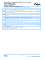
1
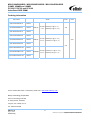
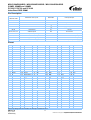
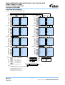
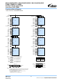
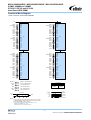
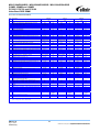
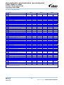
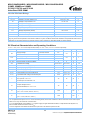
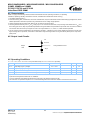
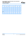
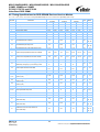
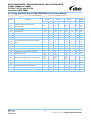
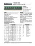
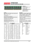
M2U51264DS8HB3G / M2U25664DS88B3G / M2U12864DSH4B3G 512MB, 256MB and 128MB PC3200, PC2700 and PC2100 Unbuffered DDR DIMM 184 pin Unbuffered DDR DIMM Based on DDR400/333/266 256M bit B Die device Features • 184 Dual In-Line Memory Module (DIMM) • DRAM DLL aligns DQ and DQS transitions with clock transitions • Unbuffered DDR DIMM based on 256M bit die B device, • Address and control signals are fully synchronous to positive organized as either 32Mbx8 or 16Mbx16 clock edge • Performance: • Programmable Operation: - DIMM CAS Latency: 2, 2.5, 3 PC3200 PC2700 PC2100 fCK tCK Speed Sort 5T 6K 75B DIMM CAS Latency 3 2.5 2.5 Clock Frequency 200 166 133 Clock Cycle fDQ DQ Burst Frequency - Burst Type: Sequential or Interleave Unit - Burst Length: 2, 4, 8 - Operation: Burst Read and Write MHz 5 6 7.5 ns 400 333 266 MHz • Auto Refresh (CBR) and Self Refresh Modes • Automatic and controlled precharge commands • 7.8 µs Max. Average Periodic Refresh Interval • Intended for 133, 166 and 200 MHz applications • Serial Presence Detect EEPROM • Inputs and outputs are SSTL-2 compatible • Gold contacts • VDD = VDDQ = 2.5V ± 0.2V (2.6V ± 0.1V for PC3200) • SDRAMs are packaged in TSOP packages • SDRAMs have 4 internal banks for concurrent operation • Differential clock inputs • Data is read or written on both clock edges Description M2U51264DS8HB3G, M2U25664DS88B3G, and M2U12864DSH4B3G are unbuffered 184-Pin Double Data Rate (DDR) Synchronous DRAM Dual In-Line Memory Modules (DIMM). M2U51264DS8HB3G is 512MB modules organized as dual ranks using sixteen 32Mx8 TSOP devices. M2U25664DS88B3G is 256MB modules organized as single rank using eight 32Mx8 TSOP devices. M2U12864DSH4B3G is 128MB modules, organized as single rank using four 16Mx16 TSOP devices. Depending on the speed grade, these DIMMs are intended for use in applications operating up to 200 MHz clock speeds and achieves high-speed data transfer rates of up to 400 MHz. Prior to any access operation, the device CAS latency and burst type/ length/operation type must be programmed into the DIMM by address inputs and I/O inputs BA0 and BA1 using the mode register set cycle. The DIMM uses a serial EEPROM and through the use of a standard IIC protocol the serial presence-detect implementation (SPD) can be accessed. The first 128 bytes of the SPD data are programmed with the module characteristics as defined by JEDEC. REV 2.2 Aug 3, 2004 Preliminary 1 © NANYA TECHNOLOGY CORPORATION NANYA reserves the right to change products and specifications without notice. M2U51264DS8HB3G / M2U25664DS88B3G / M2U12864DSH4B3G 512MB, 256MB and 128MB PC3200, PC2700 and PC2100 Unbuffered DDR DIMM Ordering Information Part Number Organization M2U51264DS8HB3G-5T 64Mx64 M2U25664DS88B3G-5T 32Mx64 M2U12864DSH4B3G-5T 16Mx64 M2U51264DS8HB3G-6K 64Mx64 M2U25664DS88B3G-6K 32Mx64 M2U12864DSH4B3G-6K Speed DDR400 DDR333 Power PC3200 200MHz (5ns @ CL = 3) 3-3-3 166MHz (6ns @ CL = 2.5) 2.6V PC2700 166MHz (6ns @ CL = 2.5) 2.5-3-3 Leads Gold 133MHz (7.5ns @ CL = 2) 16Mx64 2.5V M2U51264DS8HB3G-75B 64Mx64 M2U25664DS88B3G-75B 32Mx64 M2U12864DSH4B3G-75B DDR266B PC2100 133MHz (7.5ns @ CL = 2.5) 2.5-3-3 100MHz (10ns @ CL = 2) 16Mx64 For the closest sales office or information, please visit: www.elixir-memory.com Nanya Technology Corporation Hwa Ya Technology Park 669 Fu Hsing 3rd Rd., Kueishan, Taoyuan, 333, Taiwan, R.O.C. Tel: +886-3-328-1688 REV 2.2 Aug 3, 2004 Preliminary 2 © NANYA TECHNOLOGY CORPORATION NANYA reserves the right to change products and specifications without notice. M2U51264DS8HB3G / M2U25664DS88B3G / M2U12864DSH4B3G 512MB, 256MB and 128MB PC3200, PC2700 and PC2100 Unbuffered DDR DIMM Pin Description CK0, CK1, CK2, Differential Clock Inputs. DQ0-DQ63 Data input/output CKE0, CKE1 Clock Enable DQS0-DQS7 Bidirectional data strobes RAS Row Address Strobe DM0-DM7 Input Data Mask CAS Column Address Strobe VDD Power WE Write Enable VDDQ Supply voltage for DQs S0, S1 Chip Selects VSS Ground CK0, CK1, CK2 A0-A9, A11, A12 Address Inputs NC No Connect A10/AP Address Input/Auto-precharge SCL Serial Presence Detect Clock Input BA0, BA1 SDRAM Bank Address Inputs SDA Serial Presence Detect Data input/output VREF Ref. Voltage for SSTL_2 inputs SA0-2 Serial Presence Detect Address Inputs VDDID VDD Identification flag. VDDSPD Serial EEPROM positive power supply Pinout Pin Front Pin Back Pin Front Pin Back Pin Front 1 VREF 93 VSS 32 A5 124 VSS 62 VDDQ 154 RAS 2 DQ0 94 DQ4 33 DQ24 125 A6 63 WE 155 DQ45 3 VSS 95 DQ5 34 VSS 126 DQ28 64 DQ41 156 VDDQ 4 DQ1 96 VDDQ 35 DQ25 127 DQ29 65 CAS 157 S0 5 DQS0 97 DM0/DQS9 36 DQS3 128 VDDQ 66 VSS 158 S1 6 DQ2 98 DQ6 37 A4 129 DM3/DQS12 67 DQS5 159 DM5/DQS14 7 VDD 99 DQ7 38 VDD 130 A3 68 DQ42 160 VSS 8 DQ3 100 VSS 39 DQ26 131 DQ30 69 DQ43 161 DQ46 9 NC 101 NC 40 DQ27 132 VSS 70 VDD 162 DQ47 10 NC 102 NC 41 A2 133 DQ31 71 NC 163 NC 11 VSS 103 NC 42 VSS 134 NC 72 DQ48 164 VDDQ 12 DQ8 104 VDDQ 43 A1 135 NC 73 DQ49 165 DQ52 13 DQ9 105 DQ12 44 NC 136 VDDQ 74 VSS 166 DQ53 14 DQS1 106 DQ13 45 NC 137 CK0 75 CK2 167 NC 15 VDDQ 107 DM1/DQS10 46 VDD 138 CK0 76 CK2 168 VDD 16 CK1 108 VDD 47 NC 139 VSS 77 VDDQ 169 DM6/DQS15 17 CK1 109 DQ14 48 A0 140 NC 78 DQS6 170 DQ54 18 VSS 110 DQ15 49 NC 141 A10 79 DQ50 171 DQ55 19 DQ10 111 CKE1 50 VSS 142 NC 80 DQ51 172 VDDQ 20 DQ11 112 VDDQ 51 NC 143 VDDQ 81 VSS 173 NC 21 CKE0 113 NC 52 BA1 144 NC 82 VDDID 174 DQ60 22 VDDQ 114 DQ20 23 DQ16 115 A12 53 24 DQ17 116 VSS 25 DQS2 117 DQ21 26 VSS 118 27 A9 28 DQ18 29 30 31 DQ19 KEY KEY Pin Back 83 DQ56 175 DQ61 DQ32 145 VSS 84 DQ57 176 VSS 54 VDDQ 146 DQ36 85 VDD 177 DM7/DQS16 55 DQ33 147 DQ37 86 DQS7 178 DQ62 A11 56 DQS4 148 VDD 87 DQ58 179 DQ63 119 DM2/DQS11 57 DQ34 149 DM4/DQS13 88 DQ59 180 VDDQ 120 VDD 58 VSS 150 DQ38 89 VSS 181 SA0 A7 121 DQ22 59 BA0 151 DQ39 90 WP 182 SA1 VDDQ 122 A8 60 DQ35 152 VSS 91 SDA 183 SA2 123 DQ23 61 DQ40 153 DQ44 92 SCL 184 VDDSPD Note: All pin assignments are consistent for all 8-byte unbuffered versions. REV 2.2 Aug 3, 2004 Preliminary 3 © NANYA TECHNOLOGY CORPORATION NANYA reserves the right to change products and specifications without notice. M2U51264DS8HB3G / M2U25664DS88B3G / M2U12864DSH4B3G 512MB, 256MB and 128MB PC3200, PC2700 and PC2100 Unbuffered DDR DIMM Input/Output Functional Description Symbol CK0, CK1, CK2, CK0, CK1, CK2 CKE0, CKE1 Type (SSTL) (SSTL) Polarity Cross point Active High Function The system clock inputs. All address and command lines are sampled on the cross point of the rising edge of CK and falling edge of CK. A Delay Locked Loop (DLL) circuit is driven from the clock inputs and output timing for read operations is synchronized to the input clock. Activates the DDR SDRAM CK signal when high and deactivates the CK signal when low. By deactivating the clocks, CKE low initiates the Power Down mode or the Self Refresh mode. Enables the associated DDR SDRAM command decoder when low and disables the S0, S1 (SSTL) Active Low command decoder when high. When the command decoder is disabled, new commands are ignored but previous operations continue. Physical Bank 0 is selected by S0; Bank 1 is selected by S1. RAS, CAS, WE (SSTL) VREF Supply VDDQ Supply BA0, BA1 (SSTL) Active Low When sampled at the positive rising edge of the clock, RAS, CAS, WE define the operation to be executed by the SDRAM. Reference voltage for SSTL-2 inputs Isolated power supply for the DDR SDRAM output buffers to provide improved noise immunity - Selects which SDRAM bank is to be active. During a Bank Activate command cycle, A0-A12 defines the row address (RA0-RA12) when sampled at the rising clock edge. During a Read or Write command cycle, A0-A9 defines the column address (CA0-CA9) A0 - A9 A10/AP A11, A12 when sampled at the rising clock edge. In addition to the column address, AP is used to (SSTL) - invoke auto-precharge operation at the end of the Burst Read or Write cycle. If AP is high, auto-precharge is selected and BA0/BA1 defines the bank to be precharged. If AP is low, auto-precharge is disabled. During a Precharge command cycle, AP is used in conjunction with BA0/BA1 to control which bank(s) to precharge. If AP is high all 4 banks will be precharged regardless of the state of BA0/BA1. If AP is low, then BA0/BA1 are used to define which bank to pre-charge. DQ0 - DQ63 (SSTL) - DQS0 - DQS7, DQS9 – DQS16 (SSTL) Active High CB0 – CB7 (SSTL) - DM0 – DM8 Input Active High VDD, VSS Supply SA0 – SA2 - SDA - SCL - VDDSPD REV 2.2 Aug 3, 2004 Preliminary Supply Data and Check Bit input/output pins operate in the same manner as on conventional DRAMs. Data strobes: Output with read data, input with write data. Edge aligned with read data, centered on write data. Used to capture write data. Data Check Bit Input/Output pins. Used on ECC modules and is not used on x64 modules. The data write masks, associated with one data byte. In Write mode, DM operates as a byte mask by allowing input data to be written if it is low but blocks the write operation if it is high. In Read mode, DM lines have no effect. DM8 is associated with check bits CB0-CB7, and is not used on x64 modules. Power and ground for the DDR SDRAM input buffers and core logic Address inputs. Connected to either VDD or VSS on the system board to configure the Serial Presence Detect EEPROM address. This bi-directional pin is used to transfer data into or out of the SPD EEPROM. A resistor must be connected from the SDA bus line to V DD to act as a pull-up. This signal is used to clock data into and out of the SPD EEPROM. A resistor may be connected from the SCL bus time to V DD to act as a pull-up. Serial EEPROM positive power supply. 4 © NANYA TECHNOLOGY CORPORATION NANYA reserves the right to change products and specifications without notice. M2U51264DS8HB3G / M2U25664DS88B3G / M2U12864DSH4B3G 512MB, 256MB and 128MB PC3200, PC2700 and PC2100 Unbuffered DDR DIMM Functional Block Diagram 2 Ranks, 16 devices, 32Mx8 DDR SDRAMs S1 S0 DQS0 DM0/DQS9 DQS4 DM4/DQS13 DM I/O 7 I/O 6 I/O 1 I/O 0 I/O 5 I/O 4 I/O 3 I/O 2 DQ0 DQ1 DQ2 DQ3 DQ4 DQ5 DQ6 DQ7 CS DQS D0 DM I/O 0 I/O 1 I/O 6 I/O 7 I/O 2 I/O 3 I/O 4 I/O 5 CS DQS DQ32 DQ33 DQ34 DQ35 DQ36 DQ37 DQ38 DQ39 D8 CS DM I/O 7 I/O 6 I/O 1 I/O 0 I/O 5 I/O 4 I/O 3 I/O 2 CS DM I/O 7 I/O 6 I/O 1 I/O 0 I/O 5 I/O 4 I/O 3 I/O 2 CS DM I/O 7 I/O 6 I/O 1 I/O 0 I/O 5 I/O 4 I/O 3 I/O 2 CS DQS D4 DM I/O 0 I/O 1 I/O 6 I/O 7 I/O 2 I/O 3 I/O 4 I/O 5 CS DM I/O 0 I/O 1 I/O 6 I/O 7 I/O 2 I/O 3 I/O 4 I/O 5 CS DM I/O 0 I/O 1 I/O 6 I/O 7 I/O 2 I/O 3 I/O 4 I/O 5 CS DM I/O 0 I/O 1 I/O 6 I/O 7 I/O 2 I/O 3 I/O 4 I/O 5 CS DQS D12 DQS5 DM5/DQS14 DQS1 DM1/DQS10 DM I/O 7 I/O 6 I/O 1 I/O 0 I/O 5 I/O 4 I/O 3 I/O 2 DQ8 DQ9 DQ10 DQ11 DQ12 DQ13 DQ14 DQ15 CS DQS D1 DM I/O 0 I/O 1 I/O 6 I/O 7 I/O 2 I/O 3 I/O 4 I/O 5 CS DQS DQ40 DQ41 DQ42 DQ43 DQ44 DQ45 DQ46 DQ47 D9 DQS D5 DQS D13 DQS6 DM6/DQS15 DQS2 DM2/DQS11 DM I/O 7 I/O 6 I/O 1 I/O 0 I/O 5 I/O 4 I/O 3 I/O 2 DQ16 DQ17 DQ18 DQ19 DQ20 DQ21 DQ22 DQ23 CS DQS D2 DM I/O 0 I/O 1 I/O 6 I/O 7 I/O 2 I/O 3 I/O 4 I/O 5 CS DQS DQ48 DQ49 DQ50 DQ51 DQ52 DQ53 DQ54 DQ55 D10 DQS D6 DQS D14 DQS7 DM7/DQS16 DQS3 DM3/DQS12 DM I/O 7 I/O 6 I/O 1 I/O 0 I/O 5 I/O 4 I/O 3 I/O 2 DQ24 DQ25 DQ26 DQ27 DQ28 DQ29 DQ30 DQ31 BA0-BA1 CS D3 DQS DM I/O 0 I/O 1 I/O 6 I/O 7 I/O 2 I/O 3 I/O 4 I/O 5 BA0-BA1 : SDRAMs D0-D15 A0-A13 : SDRAMs D0-D15 A0-A13 RAS RAS : SDRAMs D0-D15 CAS CAS : SDRAMs D0-D15 CKE0 CKE : SDRAMs D0-D7 CKE1 CKE : SDRAMs D8-D15 WE Notes : 1. 2. 3. 4. DM I/O 7 I/O 6 I/O 1 I/O 0 I/O 5 I/O 4 I/O 3 I/O 2 WE : SDRAMs D0-D15 CS DQS DQ56 DQ57 DQ58 DQ59 DQ60 DQ61 DQ62 DQ63 D11 Aug 3, 2004 Preliminary Strap: see Note 4 DQS D15 * Clock Wiring Clock Input SDRAMs *CK0/CK0 4 SDRAMs *CK1/CK1 6 SDRAMs *CK2/CK2 6 SDRAMs * Wire per Clock Loading Table/ Wiring Diagrams Serial PD SCL WP DQ-to-I/O wiring is shown as recommended but may be changed. DQ/DQS/DM/CKE/S relationships must be maintained as shown. DQ, DQS, DM/DQS resistors: 22 Ohms. VDDID strap connections (for memory device VDD, VDDQ): STRAP OUT (OPEN): VDD = VDDQ STRAP IN (VSS): VDD is not equal to VDDQ. REV 2.2 SPD D0-D15 D0-D15 D0-D15 VDDSPD VDD/VDDQ VREF VSS VDDID D7 DQS A0 A1 A2 SA0 SA1 SA2 SDA 5 © NANYA TECHNOLOGY CORPORATION NANYA reserves the right to change products and specifications without notice. M2U51264DS8HB3G / M2U25664DS88B3G / M2U12864DSH4B3G 512MB, 256MB and 128MB PC3200, PC2700 and PC2100 Unbuffered DDR DIMM Functional Block Diagram 1 Rank, 8 devices, 32Mx8 DDR SDRAMs S0 DQS0 DM0/DQS9 DQS4 DM4/DQS13 DM I/O 7 I/O 6 I/O 1 I/O 0 I/O 5 I/O 4 I/O 3 I/O 2 DQ0 DQ1 DQ2 DQ3 DQ4 DQ5 DQ6 DQ7 CS DQS DQ32 DQ33 DQ34 DQ35 DQ36 DQ37 DQ38 DQ39 D0 CS DM I/O 7 I/O 6 I/O 1 I/O 0 I/O 5 I/O 4 I/O 3 I/O 2 CS DM I/O 7 I/O 6 I/O 1 I/O 0 I/O 5 I/O 4 I/O 3 I/O 2 CS DM I/O 7 I/O 6 I/O 1 I/O 0 I/O 5 I/O 4 I/O 3 I/O 2 CS DQS D4 DQS5 DM5/DQS14 DQS1 DM1/DQS10 DM I/O 7 I/O 6 I/O 1 I/O 0 I/O 5 I/O 4 I/O 3 I/O 2 DQ8 DQ9 DQ10 DQ11 DQ12 DQ13 DQ14 DQ15 CS DQS DQ40 DQ41 DQ42 DQ43 DQ44 DQ45 DQ46 DQ47 D1 DQS2 DM2/DQS11 DQS D5 DQS6 DM6/DQS15 DM I/O 7 I/O 6 I/O 1 I/O 0 I/O 5 I/O 4 I/O 3 I/O 2 DQ16 DQ17 DQ18 DQ19 DQ20 DQ21 DQ22 DQ23 CS DQS DQ48 DQ49 DQ50 DQ51 DQ52 DQ53 DQ54 DQ55 D2 DQS D6 DQS7 DM7/DQS16 DQS3 DM3/DQS12 DM I/O 7 I/O 6 I/O 1 I/O 0 I/O 5 I/O 4 I/O 3 I/O 2 DQ24 DQ25 DQ26 DQ27 DQ28 DQ29 DQ30 DQ31 BA0-BA1 CS DQS DQ56 DQ57 DQ58 DQ59 DQ60 DQ61 DQ62 DQ63 D3 DQS D7 BA0-BA1 : SDRAMs D0-D7 * Clock Wiring Clock Input SDRAMs *CK0/CK0 2 SDRAMs *CK1/CK1 3 SDRAMs *CK2/CK2 3 SDRAMs A0-A13 : SDRAMs D0-D7 A0-A13 RAS RAS : SDRAMs D0-D7 CAS CAS : SDRAMs D0-D7 CKE0 CKE : SDRAMs D0-D7 WE * Wire per Clock Loading Table/ Wiring Diagrams WE : SDRAMs D0-D7 VDDSPD VDD/VDDQ VREF VSS VDDID Serial PD SCL WP Notes : 1. 2. 3. 4. DM I/O 7 I/O 6 I/O 1 I/O 0 I/O 5 I/O 4 I/O 3 I/O 2 A0 A1 A2 SA0 SA1 SA2 SDA SPD D0-D7 D0-D7 D0-D7 Strap: see Note 4 DQ-to-I/O wiring is shown as recommended but may be changed. DQ/DQS/DM/CKE/S relationships must be maintained as shown. DQ, DQS, DM/DQS resistors: 22 Ohms. VDDID strap connections (for memory device VDD, VDDQ): STRAP OUT (OPEN): VDD = VDDQ STRAP IN (VSS): VDD is not equal to VDDQ. REV 2.2 Aug 3, 2004 Preliminary 6 © NANYA TECHNOLOGY CORPORATION NANYA reserves the right to change products and specifications without notice. M2U51264DS8HB3G / M2U25664DS88B3G / M2U12864DSH4B3G 512MB, 256MB and 128MB PC3200, PC2700 and PC2100 Unbuffered DDR DIMM Functional Block Diagram 1 Rank, 4 devices, 16Mx16 DDR SDRAMs S0 DQS1 DM1/DQS10 DQ8 DQ9 DQ10 DQ11 DQ12 DQ13 DQ14 DQ15 LDQS DQS0 DM0/DQS9 DQ0 DQ1 DQ2 DQ3 DQ4 DQ5 DQ6 DQ7 UDQS CS LDM I/O 6 I/O 4 I/O 1 I/O 3 I/O 2 I/O 0 I/O 5 I/O 7 D0 UDM I/O 8 I/O 10 I/O 15 I/O 13 I/O 12 I/O 14 I/O 11 I/O 9 DQS3 DM3/DQS12 DQ24 DQ25 DQ26 DQ27 DQ28 DQ29 DQ30 DQ31 LDQS DQS2 DM2/DQS11 DQ16 DQ17 DQ18 DQ19 DQ20 DQ21 DQ22 DQ23 UDQS CS LDM I/O 6 I/O 4 I/O 1 I/O 3 I/O 2 I/O 0 I/O 5 I/O 7 D1 UDM I/O 8 I/O 10 I/O 15 I/O 13 I/O 12 I/O 14 I/O 11 I/O 9 BA0-BA1 LDQS DQS4 DM4/DQS13 DQ32 DQ33 DQ34 DQ35 DQ36 DQ37 DQ38 DQ39 UDQS CS LDM I/O 6 I/O 4 I/O 1 I/O 3 I/O 2 I/O 0 I/O 5 I/O 7 D2 UDM I/O 8 I/O 10 I/O 15 I/O 13 I/O 12 I/O 14 I/O 11 I/O 9 DQS7 DM7/DQS16 DQ56 DQ57 DQ58 DQ59 DQ60 DQ61 DQ62 DQ63 LDQS DQS6 DM6/DQS15 DQ48 DQ49 DQ50 DQ51 DQ52 DQ53 DQ54 DQ55 UDQS CS LDM I/O 6 I/O 4 I/O 1 I/O 3 I/O 2 I/O 0 I/O 5 I/O 7 D3 UDM I/O 8 I/O 10 I/O 15 I/O 13 I/O 12 I/O 14 I/O 11 I/O 9 BA0-BA1 : SDRAMs D0-D3 * Clock Wiring Clock Input SDRAMs *CK0/CK0 NC *CK1/CK1 2 SDRAMs *CK2/CK2 2 SDRAMs A0-A13 : SDRAMs D0-D3 A0-A13 RAS RAS : SDRAMs D0-D3 CAS CAS : SDRAMs D0-D3 CKE0 CKE : SDRAMs D0-D3 WE * Wire per Clock Loading Table/ Wiring Diagrams WE : SDRAMs D0-D3 VDDSPD VDD/VDDQ VREF VSS VDDID Serial PD SCL WP Notes : 1. 2. 3. 4. DQS5 DM5/DQS14 DQ40 DQ41 DQ42 DQ43 DQ44 DQ45 DQ46 DQ47 A0 A1 A2 SA0 SA1 SA2 SDA SPD D0-D3 D0-D3 D0-D3 Strap: see Note 4 DQ-to-I/O wiring is shown as recommended but may be changed. DQ/DQS/DM/CKE/S relationships must be maintained as shown. DQ, DQS, DM/DQS resistors: 22 Ohms. VDDID strap connections (for memory device VDD, VDDQ): STRAP OUT (OPEN): VDD = VDDQ STRAP IN (VSS): VDD is not equal to VDDQ. REV 2.2 Aug 3, 2004 Preliminary 7 © NANYA TECHNOLOGY CORPORATION NANYA reserves the right to change products and specifications without notice. M2U51264DS8HB3G / M2U25664DS88B3G / M2U12864DSH4B3G 512MB, 256MB and 128MB PC3200, PC2700 and PC2100 Unbuffered DDR DIMM Serial Presence Detect SPD Description Byte 0 Description Number of Serial PD Bytes Written during Production Byte 26 Description Maximum Data Access Time from Clock at CL=1 1 Total Number of Bytes in Serial PD device 27 Minimum Row Precharge Time (tRP) 2 Fundamental Memory Type 28 Minimum Row Active to Row Active delay (tRRD) 3 Number of Row Addresses on Assembly 29 Minimum RAS to CAS delay (tRCD) 4 Number of Column Addresses on Assembly 30 Minimum RAS Pulse Width (tRAS) 5 Number of DIMM Rank 31 Module Bank Density 6 Data Width of Assembly 32 Address and Command Setup Time Before Clock 7 Data Width of Assembly (cont’) 33 Address and Command Hold Time After Clock 8 Voltage Interface Level of this Assembly 34 Data Input Setup Time Before Clock 35 Data Input Hold Time After Clock 9 10 DDR SDRAM Device Cycle Time CL=2.5 DDR SDRAM Device Access Time from Clock 36-40 CL=2.5 Reserved 11 DIMM Configuration Type 41 12 Refresh Rate/Type 42 13 Primary DDR SDRAM Width 43 Max Cycle Time (tCK max) 14 Error Checking DDR SDRAM Device Width 44 Maximum DQS-DQ Skew Time (tDQSQ) 45 Maximum Read Data Hold Skew Factor (tQHS) 15 16 17 18 DDR SDRAM Device Attr: Min CLK Delay, Random Col Access DDR SDRAM Device Attributes: Burst Length 46-61 Supported DDR SDRAM Device Attributes: Number of Device Banks DDR SDRAM Device Attributes: CAS Latencies Supported Minimum Active/Auto-refresh Time (tRC) Auto-refresh to Active/Auto-refresh Command Period (tRFC) Reserved 62 SPD Revision 63 Checksum Data 19 DDR SDRAM Device Attributes: CS Latency 64-71 20 DDR SDRAM Device Attributes: WE Latency 72 21 DDR SDRAM Device Attributes: 73-90 22 DDR SDRAM Device Attributes: General 91-92 Manufacturer’s JEDEC ID Code Module Manufacturing Location Module Part number Module Revision Code Module Manufacturing Data 23 yy= Binary coded decimal year code, 0-99(Decimal), Minimum Clock Cycle 93-94 CL=2.5 00-63(Hex) ww= Binary coded decimal year code, 01-52(Decimal), 01-34(Hex) 24 25 Maximum Data Access Time from Clock at 95-98 Module Serial Number 99-127 Reserved CL=2 Minimum Clock Cycle Time at CL=1 REV 2.2 Aug 3, 2004 Preliminary 8 © NANYA TECHNOLOGY CORPORATION NANYA reserves the right to change products and specifications without notice. M2U51264DS8HB3G / M2U25664DS88B3G / M2U12864DSH4B3G 512MB, 256MB and 128MB PC3200, PC2700 and PC2100 Unbuffered DDR DIMM SPD Values for M2U51264DS8HB3G Byte Description 0 1 2 3 4 5 6. 7 8 9 10 11 12 Number of Serial PD Bytes Written during Production Total Number of Bytes in Serial PD device Fundamental Memory Type Number of Row Addresses on Assembly Number of Column Addresses on Assembly Number of DIMM Bank Data Width of Assembly Data Width of Assembly (cont’) Voltage Interface Level of this Assembly DDR SDRAM Device Cycle Time at CL=3 DDR SDRAM Device Access Time from Clock at CL=3 DIMM Configuration Type Refresh Rate/Type 13 14 15 DDR400 -5T SPD Value hexadecimal 128 80 256 08 DDR SDRAM 07 13 0D 10 0A 2 02 X64 40 X64 00 SSTL 2.5V 04 5ns 50 0.6ns 60 Non-Parity 00 SR/1x(7.8us), 82 Self Refresh Flag X8 08 N/A 00 1 Clock 01 DDR333 -6K SPD Value hexadecimal 128 80 256 08 DDR SDRAM 07 13 0D 10 0A 2 02 X64 40 X64 00 SSTL 2.5V 04 6ns 60 0.7ns 70 Non-Parity 00 SR/1x(7.8us), 82 Self Refresh Flag X8 08 N/A 00 1 Clock 01 DDR266 -75B SPD Value hexadecimal 128 80 256 08 DDR SDRAM 07 13 0D 10 0A 2 02 X64 40 X64 00 SSTL 2.5V 04 7.5ns 75 0.75ns 75 Non-Parity 00 SR/1x(7.8us), 82 Self Refresh Flag X8 08 N/A 00 1 Clock 01 Primary DDR SDRAM Width Error Checking DDR SDRAM Device Width DDR SDRAM Device Attr: Min Clk Delay, Random Col Access 16 DDR SDRAM Device Attributes: Burst Length Supported 2,4,8 0E 2,4,8 0E 2,4,8 0E 17 DDR SDRAM Device Attributes: Number of Device Banks 4 04 4 04 4 04 18 DDR SDRAM Device Attributes: CAS Latencies Supported 2/2.5/3 1C 2/2.5 0C 2/2.5 0C 19 DDR SDRAM Device Attributes: CS Latency 0 01 0 01 0 01 20 DDR SDRAM Device Attributes: WE Latency 1 02 1 02 1 02 21 DDR SDRAM Device Attributes: Differential Clock 20 Differential Clock 20 Differential Clock 20 22 DDR SDRAM Device Attributes: General +/-0.2V Voltage 00 +/-0.2V Voltage 00 +/-0.2V Voltage 00 Tolerance Tolerance Tolerance 23 Minimum Clock Cycle at CL=2.5 6.0ns 60 7.5ns 75 10ns A0 24 Maximum Data Access Time (tAC) from Clock at CL=2.5 0.7ns 70 0.70ns 70 0.75ns 75 25 Minimum Clock Cycle Time at CL=2 7.5ns 75 N/A 00 N/A 00 26 Maximum Data Access Time (tAC) from Clock at CL=2 7.5ns 75 N/A 00 N/A 00 27 Minimum Row Precharge Time (tRP) 15ns 3C 18ns 48 20ns 50 28 Minimum Row Active to Row Active delay (tRRD) 10ns 28 12ns 30 15ns 3C 29 Minimum RAS to CAS delay (tRCD) 15ns 3C 18ns 48 20ns 50 30 Minimum RAS Pulse Width (tRAS) 40ns 28 42ns 2A 45ns 2D 31 Module Bank Density 256MB 40 256MB 40 256MB 40 32 Address and Command Setup Time Before Clock 0.6ns 60 0.75ns 75 0.9ns 90 33 Address and Command Hold Time After Clock 0.6ns 60 0.75ns 75 0.9ns 90 34 Data Input Setup Time Before Clock 0.4ns 40 0.45ns 45 0.5ns 50 35 Data Input Hold Time After Clock 0.4ns 40 0.45ns 45 0.5ns 50 36-40 Reserved Undefined 00 Undefined 00 Undefined 00 41 Minimum Active/Auto-Refresh Time (tRC) 55ns 37 60ns 3C 65ns 41 42 SDRAM Device Minimum Auto-Refresh to Active/Auto 70ns 46 72ns 48 75ns 4B Refresh Command Period (tRFC) 43 SDRAM Device Maximum Cycle Time (tCK max) 8 20 12 30 12 30 44 SDRAM Device Maximum DQS-DQ Skew Time (tDQSQ) 0.4 28 0.4 28 0.5 32 45 SDRAM Device Maximum Read Data Hold Skew Factor 0.5 50 0.55 55 0.75 75 (tQHS) 46 Superset Information (may be used in future) Undefined 00 Undefined 00 Undefined 00 47 SDRAM device Attributes – DDR SDRAM DIMM Height 31.75mm 01 31.75mm 01 31.75mm 01 48-61 Superset Information (may be used in future) Undefined 00 Undefined 00 Undefined 00 62 SPD Revision 1.0 10 1.0 10 1.0 10 63 Checksum Data A0 4D 34 64-71 Manufacturer’s JEDED ID Code 0B Hex bank 3 7F7F7F0B000 0B Hex bank 3 7F7F7F0B000 0B Hex bank 3 7F7F7F0B000 00000 00000 00000 72 Module Manufacturing Location Note1 Note1 Note1 73-25 Reserved Undefined Note 2 Undefined Note 2 Undefined Note 2 5 1. please refer to BNDCJ-0082 2. byte 73-255 please refer to NDCJ-0969 REV 2.2 Aug 3, 2004 Preliminary 9 © NANYA TECHNOLOGY CORPORATION NANYA reserves the right to change products and specifications without notice. M2U51264DS8HB3G / M2U25664DS88B3G / M2U12864DSH4B3G 512MB, 256MB and 128MB PC3200, PC2700 and PC2100 Unbuffered DDR DIMM SPD Values for M2U25664DS88B3G Byte Description 0 1 2 3 4 5 6. 7 8 9 10 11 12 Number of Serial PD Bytes Written during Production Total Number of Bytes in Serial PD device Fundamental Memory Type Number of Row Addresses on Assembly Number of Column Addresses on Assembly Number of DIMM Bank Data Width of Assembly Data Width of Assembly (cont’) Voltage Interface Level of this Assembly DDR SDRAM Device Cycle Time at CL=3 DDR SDRAM Device Access Time from Clock at CL=3 DIMM Configuration Type Refresh Rate/Type 13 14 15 DDR400 -5T SPD Value hexadecimal 128 80 256 08 DDR SDRAM 07 13 0D 10 0A 1 01 X64 40 X64 00 SSTL 2.5V 04 5ns 50 0.6ns 60 Non-Parity 00 SR/1x(7.8us), 82 Self Refresh Flag X8 08 N/A 00 1 Clock 01 DDR333 -6K SPD Value hexadecimal 128 80 256 08 DDR SDRAM 07 13 0D 10 0A 1 01 X64 40 X64 00 SSTL 2.5V 04 6ns 60 0.7ns 70 Non-Parity 00 SR/1x(7.8us), 82 Self Refresh Flag X8 08 N/A 00 1 Clock 01 DDR266 -75B SPD Value hexadecimal 128 80 256 08 DDR SDRAM 07 13 0D 10 0A 1 01 X64 40 X64 00 SSTL 2.5V 04 7.5ns 75 0.75ns 75 Non-Parity 00 SR/1x(7.8us), 82 Self Refresh Flag X8 08 N/A 00 1 Clock 01 Primary DDR SDRAM Width Error Checking DDR SDRAM Device Width DDR SDRAM Device Attr: Min Clk Delay, Random Col Access 16 DDR SDRAM Device Attributes: Burst Length Supported 2,4,8 0E 2,4,8 0E 2,4,8 0E 17 DDR SDRAM Device Attributes: Number of Device Banks 4 04 4 04 4 04 18 DDR SDRAM Device Attributes: CAS Latencies Supported 2/2.5/3 1C 2/2.5 0C 2/2.5 0C 19 DDR SDRAM Device Attributes: CS Latency 0 01 0 01 0 01 20 DDR SDRAM Device Attributes: WE Latency 1 02 1 02 1 02 21 DDR SDRAM Device Attributes: Differential Clock 20 Differential Clock 20 Differential Clock 20 22 DDR SDRAM Device Attributes: General +/-0.2V Voltage 00 +/-0.2V Voltage 00 +/-0.2V Voltage 00 Tolerance Tolerance Tolerance 23 Minimum Clock Cycle at CL=2.5 6.0ns 60 7.5ns 75 10ns A0 24 Maximum Data Access Time (tAC) from Clock at CL=2.5 0.7ns 70 0.70ns 70 0.75ns 75 25 Minimum Clock Cycle Time at CL=2 7.5ns 75 N/A 00 N/A 00 26 Maximum Data Access Time (tAC) from Clock at CL=2 7.5ns 75 N/A 00 N/A 00 27 Minimum Row Precharge Time (tRP) 15ns 3C 18ns 48 20ns 50 28 Minimum Row Active to Row Active delay (tRRD) 10ns 28 12ns 30 15ns 3C 29 Minimum RAS to CAS delay (tRCD) 15ns 3C 18ns 48 20ns 50 30 Minimum RAS Pulse Width (tRAS) 40ns 28 42ns 2A 45ns 2D 31 Module Bank Density 256MB 40 256MB 40 256MB 40 32 Address and Command Setup Time Before Clock 0.6ns 60 0.75ns 75 0.9ns 90 33 Address and Command Hold Time After Clock 0.6ns 60 0.75ns 75 0.9ns 90 34 Data Input Setup Time Before Clock 0.4ns 40 0.45ns 45 0.5ns 50 35 Data Input Hold Time After Clock 0.4ns 40 0.45ns 45 0.5ns 50 36-40 Reserved Undefined 00 Undefined 00 Undefined 00 41 Minimum Active/Auto-Refresh Time (tRC) 55ns 37 60ns 3C 65ns 41 42 SDRAM Device Minimum Auto-Refresh to Active/Auto 70ns 46 72ns 48 75ns 4B Refresh Command Period (tRFC) 43 SDRAM Device Maximum Cycle Time (tCK max) 8 20 12 30 12 30 44 SDRAM Device Maximum DQS-DQ Skew Time (tDQSQ) 0.4 28 0.4 28 0.5 32 45 SDRAM Device Maximum Read Data Hold Skew Factor 0.5 50 0.55 55 0.75 75 (tQHS) 46 Superset Information (may be used in future) Undefined 00 Undefined 00 Undefined 00 47 SDRAM device Attributes – DDR SDRAM DIMM Height 31.75mm 01 31.75mm 01 31.75mm 01 48-61 Superset Information (may be used in future) Undefined 00 Undefined 00 Undefined 00 62 SPD Revision 1.0 10 1.0 10 1.0 10 63 Checksum Data 9F 4C 33 64-71 Manufacturer’s JEDED ID Code 0B Hex bank 3 7F7F7F0B000 0B Hex bank 3 7F7F7F0B000 0B Hex bank 3 7F7F7F0B000 00000 00000 00000 72 Module Manufacturing Location Note1 Note1 Note1 73-25 Reserved Undefined Note 2 Undefined Note 2 Undefined Note 2 5 3. please refer to BNDCJ-0082 4. byte 73-255 please refer to NDCJ-0969 REV 2.2 Aug 3, 2004 Preliminary 10 © NANYA TECHNOLOGY CORPORATION NANYA reserves the right to change products and specifications without notice. M2U51264DS8HB3G / M2U25664DS88B3G / M2U12864DSH4B3G 512MB, 256MB and 128MB PC3200, PC2700 and PC2100 Unbuffered DDR DIMM SPD Values for M2U12864DSH4B3G Byte Description DDR400 -5T SPD Value hexadecimal 0 1 2 3 4 5 6. 7 8 9 10 11 12 Number of Serial PD Bytes Written during Production Total Number of Bytes in Serial PD device Fundamental Memory Type Number of Row Addresses on Assembly Number of Column Addresses on Assembly Number of DIMM Bank Data Width of Assembly Data Width of Assembly (cont’) Voltage Interface Level of this Assembly DDR SDRAM Device Cycle Time at CL=3 DDR SDRAM Device Access Time from Clock at CL=3 DIMM Configuration Type Refresh Rate/Type 13 14 15 Primary DDR SDRAM Width X16 Error Checking DDR SDRAM Device Width N/A DDR SDRAM Device Attr: Min Clk Delay, Random Col 1 Clock Access DDR SDRAM Device Attributes: Burst Length Supported 2,4,8 DDR SDRAM Device Attributes: Number of Device Banks 4 DDR SDRAM Device Attributes: CAS Latencies Supported 2/2.5/3 DDR SDRAM Device Attributes: CS Latency 0 DDR SDRAM Device Attributes: WE Latency 1 DDR SDRAM Device Attributes: Differential Clock DDR SDRAM Device Attributes: General +/-0.2V Voltage 16 17 18 19 20 21 22 23 24 25 26 27 28 29 30 31 32 33 34 35 36-40 41 42 Minimum Clock Cycle at CL=2.5 Maximum Data Access Time (tAC) from Clock at CL=2.5 Minimum Clock Cycle Time at CL=2 Maximum Data Access Time (tAC) from Clock at CL=2 Minimum Row Precharge Time (tRP) Minimum Row Active to Row Active delay (tRRD) Minimum RAS to CAS delay (tRCD) Minimum RAS Pulse Width (tRAS) Module Bank Density Address and Command Setup Time Before Clock Address and Command Hold Time After Clock Data Input Setup Time Before Clock Data Input Hold Time After Clock Reserved Minimum Active/Auto-Refresh Time (tRC) SDRAM Device Minimum Auto-Refresh to Active/Auto Refresh Command Period (tRFC) 43 SDRAM Device Maximum Cycle Time (tCK max) 44 SDRAM Device Maximum DQS-DQ Skew Time (tDQSQ) 45 SDRAM Device Maximum Read Data Hold Skew Factor (tQHS) 46 Superset Information (may be used in future) 47 SDRAM device Attributes – DDR SDRAM DIMM Height 48-61 Superset Information (may be used in future) 62 SPD Revision 63 Checksum Data 64-71 Manufacturer’s JEDED ID Code 72 73-25 5 5. 6. Module Manufacturing Location Reserved 128 256 DDR SDRAM 13 9 1 X64 X64 SSTL 2.5V 5ns 0.6ns Non-Parity SR/1x(7.8us), DDR333 -6K SPD Value hexadecimal 80 08 07 0D 09 01 40 00 04 50 60 00 82 128 256 DDR SDRAM 13 9 1 X64 X64 SSTL 2.5V 6ns 0.7ns Non-Parity SR/1x(7.8us), 80 08 07 0D 09 01 40 00 04 60 70 00 82 10 00 01 X16 N/A 1 Clock 10 00 01 0E 04 1C 01 02 20 00 2,4,8 4 2/2.5 0 1 Differential Clock +/-0.2V Voltage 0E 04 0C 01 02 20 00 6.0ns 0.7ns 7.5ns 7.5ns 15ns 10ns 15ns 40ns 128MB 0.6ns 0.6ns 0.4ns 0.4ns Undefined 55ns 70ns 60 70 75 75 3C 28 3C 28 20 60 60 40 40 00 37 46 7.5ns 0.70ns N/A N/A 18ns 12ns 18ns 42ns 128MB 0.75ns 0.75ns 0.45ns 0.45ns Undefined 60ns 72ns 8 0.4 0.5 20 28 50 Undefined 31.75mm Undefined 1.0 00 01 00 10 86 7F7F7F0B000 00000 Note1 Note 2 0B Hex bank 3 Undefined DDR266 -75B SPD Value hexadecimal 128 256 DDR SDRAM 13 9 1 X64 X64 SSTL 2.5V 75ns 0.75ns Non-Parity SR/1x(7.8us), Self Refresh Flag X16 N/A 1 Clock 80 08 07 0D 09 01 40 00 04 75 75 00 82 0E 04 0C 01 02 20 00 75 70 00 00 48 30 48 2A 20 75 75 45 45 00 3C 48 2,4,8 4 2/2.5 0 1 Differential Clock +/-0.2V Voltage Tolerance 10ns 0.75ns N/A N/A 20ns 15ns 20ns 45ns 128MB 0.9ns 0.9ns 0.5ns 0.5ns Undefined 65ns 75ns A0 75 00 00 50 3C 50 2D 20 90 90 50 50 00 41 4B 12 0.4 0.55 30 28 55 12 0.5 0.75 30 32 75 Undefined 31.75mm Undefined 1.0 00 01 00 10 33 7F7F7F0B000 00000 Note1 Note 2 Undefined 31.75mm Undefined 1.0 00 01 00 10 1A 7F7F7F0B000 00000 Note1 Note 2 0B Hex bank 3 Undefined 0B Hex bank 3 Undefined 10 00 01 please refer to BNDCJ-0082 byte 73-255 please refer to NDCJ-0969 REV 2.2 Aug 3, 2004 Preliminary 11 © NANYA TECHNOLOGY CORPORATION NANYA reserves the right to change products and specifications without notice. M2U51264DS8HB3G / M2U25664DS88B3G / M2U12864DSH4B3G 512MB, 256MB and 128MB PC3200, PC2700 and PC2100 Unbuffered DDR DIMM Absolute Maximum Ratings Symbol VIN, VOUT Parameter Voltage on I/O pins relative to VSS Rating Units -0.5 to VDDQ +0.5 V VIN Voltage on Input relative to VSS -0.5 to +3.6 V VDD Voltage on VDD supply relative to VSS -0.5 to +3.6 V VDDQ Voltage on VDDQ supply relative to VSS -0.5 to +3.6 V 0 to +70 °C -55 to +150 °C TA TSTG Operating Temperature (Ambient) Storage Temperature (Plastic) PD Power Dissipation (per device component) 1 W IOUT Short Circuit Output Current 50 mA Note: Stresses greater than those listed under “Absolute Maximum Ratings” may cause permanent damage to the device. This is stress rating only, and functional operation of the device at these or any other conditions above those indicated in the operational sections of this specification is not implied. Exposure to absolute maximum rating conditions for extended periods may affect reliability. DC Electrical Characteristics and Operating Conditions TA= 0°C ~ 70°C; VDDQ= VDD= 2.5V±0.2V(PC2100,PC2700); TA= 0°C ~ 70°C; VDDQ= VDD= 2.6V±0.1V(PC3200) Symbol VDD VDDQ VSS, VSSQ Parameter Supply Voltage I/O Supply Voltage Min Max Units Notes 2.7 V 1 2.7 V 1 0 0 V PC2100, PC2700 2.3 PC3200 2.5 PC2100, PC2700 2.3 PC3200 2.5 Supply Voltage, I/O Supply Voltage VREF I/O Reference Voltage 0.49 x VDDQ 0.51 x VDDQ V 1, 2 VTT I/O Termination Voltage (System) VREF – 0.04 VREF + 0.04 V 1, 3 VIH (DC) Input High (Logic1) Voltage VREF + 0.15 VDDQ + 0.3 V 1 VIL (DC) Input Low (Logic0) Voltage -0.3 VREF - 0.15 V 1 VIN (DC) Input Voltage Level, CK and CK Inputs -0.3 VDDQ + 0.3 V 1 Input Differential Voltage, CK and CK Inputs 0.30 VDDQ + 0.6 V 1, 4 -10 10 µA 1 -10 10 µA 1 -16.8 - mA 1 16.8 - mA 1 VID (DC) Input Leakage Current II Any input 0V ≤ VIN ≤ VDD; All other pins not under test = 0V IOZ IOH IOL Output Leakage Current DQs are disabled; 0V ≤ Vout ≤ VDDQ Output High Current (VOUT = VDDQ -0.373V, min VREF, min VTT) Output Low Current (VOUT = 0.373, max VREF, max VTT) 1. Inputs are not recognized as valid until VREF stabilizes. 2. VREF is expected to be equal to 0.5 VDDQ of the transmitting device, and to track variations in the DC level of the same. Peak-to-peak noise on VREF may not exceed 2% of the DC value. 3. VTT is not applied directly to the DIMM. VTT is a system supply for signal termination resistors, is expected to be set equal to VREF, and must track variations in the DC level of VREF. 4. VID is the magnitude of the difference between the input level on CK and the input level on CK. REV 2.2 Aug 3, 2004 Preliminary 12 © NANYA TECHNOLOGY CORPORATION NANYA reserves the right to change products and specifications without notice. M2U51264DS8HB3G / M2U25664DS88B3G / M2U12864DSH4B3G 512MB, 256MB and 128MB PC3200, PC2700 and PC2100 Unbuffered DDR DIMM AC Characteristics Notes 1-5 apply to the following Tables; Electrical Characteristics and DC Operating Conditions, AC Operating Conditions, Operating, Standby, and Refresh Currents, and Electrical Characteristics and AC Timing.) 1. All voltages referenced to VSS. 2. Tests for AC timing, IDD, and electrical, AC and DC characteristics, may be conducted at nominal reference/supply voltage levels, but the related specifications and device operation are guaranteed for the full voltage range specified. 3. Outputs measured with equivalent load. Refer to the AC Output Load Circuit below. 4. AC timing and IDD tests may use a VIL to VIH swing of up to 1.5V in the test environment, but input timing is still referenced to VREF (or to the crossing point for CK, CK), and parameter specifications are guaranteed for the specified AC input levels under normal use conditions. The minimum slew rate for the input signals is 1V/ns in the range between VIL (AC) and VIH (AC) unless otherwise specified. 5. The AC and DC input level specifications are as defined in the SSTL_2 Standard (i.e. the receiver effectively switches as a result of the signal crossing the AC input level, and remains in that state as long as the signal does not ring back above (below) the DC input LOW (HIGH) level. AC Output Load Circuits VTT 50 ohms Output Timing Reference Point VOUT 30 pF AC Operating Conditions TA = 0 °C ~ 70 °C; VDDQ= VDD= 2.5V ± 0.2V (PC2100/PC2700); VDDQ= VDD= 2.6V ± 0.1V (PC3200) Symbol Parameter/Condition Min VIH (AC) Input High (Logic 1) Voltage. VIL (AC) Input Low (Logic 0) Voltage. VID (AC) Input Differential Voltage, CK and CK Inputs VIX (AC) Input Differential Pair Cross Point Voltage, CK and CK Inputs Max Unit Notes V 1, 2 VREF - 0.31 V 1, 2 0.62 VDDQ + 0.6 V 1, 2, 3 (0.5* VDDQ) - 0.2 (0.5* VDDQ) + 0.2 V 1, 2, 4 VREF + 0.31 1. Input slew rate = 1V/ ns. 2. Inputs are not recognized as valid until VREF stabilizes. 3. VID is the magnitude of the difference between the input level on CK and the input level on CK. 4. The value of VIX is expected to equal 0.5*VDDQ of the transmitting device and must track variations in the DC level of the same. REV 2.2 Aug 3, 2004 Preliminary 13 © NANYA TECHNOLOGY CORPORATION NANYA reserves the right to change products and specifications without notice. M2U51264DS8HB3G / M2U25664DS88B3G / M2U12864DSH4B3G 512MB, 256MB and 128MB PC3200, PC2700 and PC2100 Unbuffered DDR DIMM Operating, Standby, and Refresh Currents TA = 0 °C ~ 70 °C; VDDQ= VDD= 2.5V ± 0.2V (PC2100/PC2700); VDDQ= VDD= 2.6V ± 0.1V (PC3200) Symbol IDD0 IDD1 IDD2P IDD2N IDD3P IDD3N IDD4R IDD4W Parameter/Condition clock cycle; address and control inputs changing once per clock cycle Operating Current: one bank; active/read/precharge; Burst = 2; tRC = tRC (MIN); CL=2.5; tCK = tCK (MIN); IOUT = 0mA; address and control inputs changing once per clock cycle Precharge Power-Down Standby Current: all banks idle; power-down mode; CKE ≤ VIL (MAX); tCK = tCK (MIN) Idle Standby Current: CS ≥ VIH (MIN); all banks idle; CKE ≥ VIH (MIN); tCK = tCK (MIN); address and control inputs changing once per clock cycle Active Power-Down Standby Current: one bank active; power-down mode; CKE ≤ VIL (MAX); tCK = tCK (MIN) Active Standby Current: one bank; active/precharge; CS ≥ VIH (MIN); CKE ≥ VIH (MIN); tRC = tRAS (MAX); tCK = tCK (MIN); DQ, DM, and DQS inputs changing twice per clock cycle; address and control inputs changing once per clock cycle Operating Current: one bank; Burst = 2; reads; continuous burst; address and control inputs changing once per clock cycle; DQ and DQS outputs changing twice per clock cycle; CL = 2.5; tCK = tCK (MIN); IOUT = 0mA Operating Current: one bank; Burst = 2; writes; continuous burst; address and control inputs changing once per clock cycle; DQ and DQS inputs changing twice per clock cycle; CL=2.5; tCK = tCK (MIN) IDD5 Auto-Refresh Current: tRC = tRFC (MIN) IDD6 Self-Refresh Current: CKE ≤ 0.2V IDD7 Notes Operating Current: one bank; active/precharge; tRC = tRC (MIN); tCK = tCK (MIN); DQ, DM, and DQS inputs changing twice per 1,2 1,2 1,2 1,2 1,2 1,2 1,2 1,2 1,2,3 1,2 Operating Current: four bank; four bank interleaving with BL = 4, address and control inputs randomly changing; 50% of data changing at every transfer; tRC = tRC (min); IOUT = 0mA. 1,2 1. IDD specifications are tested after the device is properly initialized. 2. Input slew rate = 1V/ ns. 3. Current at 7.8 µs is time averaged value of IDD5 at tRFC (MIN) and IDD2P over 7.8 µs. All IDD current values are calculated from device level. REV 2.2 Aug 3, 2004 Preliminary 14 © NANYA TECHNOLOGY CORPORATION NANYA reserves the right to change products and specifications without notice. M2U51264DS8HB3G / M2U25664DS88B3G / M2U12864DSH4B3G 512MB, 256MB and 128MB PC3200, PC2700 and PC2100 Unbuffered DDR DIMM M2U51264DS8HB3G Symbol M2U25664DS88B3G M2U12864DSH4B3G PC3200 PC2700 PC2100 PC3200 PC2700 PC2100 PC3200 PC2700 PC2100 (5T) (6K) (75B) (5T) (6K) (75B) (5T) (6K) (75B) IDD0 1915 1755 1585 995 915 825 460 420 380 IDD1 1995 1995 1825 1035 1035 945 480 480 440 IDD2P 340 340 340 180 180 180 80 80 80 IDD2N 765 765 680 405 405 360 180 180 160 IDD3P 357 357 306 189 189 162 84 84 72 IDD3N 1275 1275 1105 675 675 585 300 300 260 IDD4R 3275 3275 2705 1675 1675 1385 800 800 660 IDD4W 3195 3195 2625 1635 1635 1345 780 780 640 IDD5 3675 2875 2785 1875 1475 1425 900 700 680 IDD6 51 51 51 27 27 27 12 12 12 IDD7 5275 5275 4065 2675 2675 2065 1300 1300 1000 REV 2.2 Aug 3, 2004 Preliminary 15 © NANYA TECHNOLOGY CORPORATION NANYA reserves the right to change products and specifications without notice. M2U51264DS8HB3G / M2U25664DS88B3G / M2U12864DSH4B3G 512MB, 256MB and 128MB PC3200, PC2700 and PC2100 Unbuffered DDR DIMM AC Timing Specifications for DDR SDRAM Devices Used on Module TA = 0 °C ~ 70 °C; VDDQ= VDD= 2.5V ± 0.2V (PC2100/PC2700); VDDQ= VDD= 2.6V ± 0.1V (PC3200) (Part 1 of 2) Symbol Parameter 5T 6K 75B PC3200 PC2700 PC2100 Unit Notes Min. Max. Min. Max. Min. Max. DQ output access time from CK/CK -0.65 +0.65 -0.7 +0.7 -0.75 +0.75 ns 1-4 DQS output access time from CK/CK -0.55 +0.55 -0.7 +0.7 -0.75 +0.75 ns 1-4 tCH CK high-level width 0.45 0.55 0.45 0.55 0.45 0.55 tCK 1-4 tCL CK low-level width 0.45 0.55 0.45 0.55 0.45 0.55 tCK 1-4 tCK Clock cycle time CL=3 5 8 - - - - tCK Clock cycle time CL=2.5 6 12 6 12 7.5 12 ns 1-4 tCK Clock cycle time CL=2 - - 7.5 12 10 12 ns 1-4 tDH DQ and DM input hold time 0.4 0.45 0.5 ns tDS DQ and DM input setup time 0.4 0.45 0.5 ns tDIPW DQ and DM input pulse width (each input) 1.75 1.75 1.75 ns 1-4 tHZ Data-out high-impedance time from CK/CK -0.6 +0.6 -0.7 +0.7 -0.75 +0.75 ns 1-4, 5 tLZ Data-out low-impedance time from CK/CK -0.6 +0.6 -0.7 +0.7 -0.75 +0.75 ns 1-4, 5 0.5 ns 1-4 tCK 1-4 tCK 1-4 0.75 ns 1-4 1.25 tCK 1-4 tAC tDQSCK tDQSQ tHP DQS-DQ skew (DQS & associated DQ signals) 0.4 0.45 Minimum half clk period for any given cycle; tCH or tCH or tCH or defined by clk high (tCH) or clk low (tCL) time tCL tCL tCL tHP - tHP - tHP - tQHS tQHS tQHS tQH Data output hold time from DQS tQHS Data hold Skew Factor tDQSS Write command to 1st DQS latching transition tDQSL, DQS input low (high) pulse width tDQSH (write cycle) 0.5 0.75 1.25 0.55 0.75 1.25 0.75 1-4, 15, 16 1-4, 15, 16 0.35 0.35 0.35 tCK 1-4 0.2 0.2 0.2 tCK 1-4 0.2 0.2 0.2 tCK 1-4 Mode register set command cycle time 2 2 2 tCK 1-4 tWPRES Write preamble setup time 0 0 0 ns 1-4, 7 tWPST Write postamble 0.40 tCK 1-4, 6 tWPRE Write preamble 0.25 0.25 0.25 tCK 1-4 0.6 0.75 0.9 ns 0.6 0.75 0.9 ns 0.7 0.8 1.0 ns tDSS tDSH tMRD tIH tIS tIH DQS falling edge to CK setup time (write cycle) DQS falling edge hold time from CK (write cycle) Address and control input hold time (fast slew rate) Address and control input setup time (fast slew rate) Address and control input hold time (slow slew rate) REV 2.2 Aug 3, 2004 Preliminary 0.60 0.40 0.60 0.40 0.60 2-4, 9, 11, 12 2-4, 9, 11, 12 2-4, 10, 11, 12, 14 16 © NANYA TECHNOLOGY CORPORATION NANYA reserves the right to change products and specifications without notice. M2U51264DS8HB3G / M2U25664DS88B3G / M2U12864DSH4B3G 512MB, 256MB and 128MB PC3200, PC2700 and PC2100 Unbuffered DDR DIMM AC Timing Specifications for DDR SDRAM Devices Used on Module TA = 0 °C ~ 70 °C; VDDQ= VDD= 2.5V ± 0.2V (PC2100/PC2700); VDDQ= VDD= 2.6V ± 0.1V (PC3200) (Part 2 of 2) Symbol Parameter 5T 6K 75B PC3200 PC2700 PC2100 Min. tIS tIPW Address and control input setup time (slow slew rate) Max. Min. Max. Min. 0.7 0.8 14 2.2 ns 2-4, 12 1.1 tCK 1-4 0.40 0.60 tCK 1-4 45ns 120us tRP RE Read preamble 0.9 1.1 0.9 1.1 0.9 tRP ST Read postamble 0.40 0.60 0.40 0.60 tRAS Active to Precharge command 42ns 120us 42ns 120us tRC Active to Active/Auto-refresh command period period ns 10-12, Max. 1.0 2.2 Auto-refresh to Active/Auto-refresh command Notes 2-4, Input pulse width tRFC Unit 2.2 1-4 55 60 65 ns 1-4 70 72 75 ns 1-4 tRCD Active to Read or Write delay 15 18 20 ns 1-4 tRAP Active to Read Command with Auto-precharge 15 18 20 ns 1-4 tRP Precharge command period 15 18 20 ns 1-4 tRRD Active bank A to Active bank B command 10 12 15 ns 1-4 tWR Write recovery time 15 (tWR/ tCK ) + (tRP / tCK ) 1-4 Auto-precharge write recovery + precharge time 15 (tWR/ tCK ) + (tRP / tCK ) ns tDAL 15 (tWR/ tCK ) + (tRP / tCK ) tCK 1-4, 13 tWTR Internal write to read command delay 1 1 1 tCK 1-4 tPDEX Power down exit time 5 6 7.5 ns 1-4 tXSNR Exit self-refresh to non-read command 75 75 75 ns 1-4 tXSRD Exit self-refresh to read command 200 200 200 tCK 1-4 tREFI Average Periodic Refresh Interval µs 1-4, 8 REV 2.2 Aug 3, 2004 Preliminary 7.8 7.8 7.8 17 © NANYA TECHNOLOGY CORPORATION NANYA reserves the right to change products and specifications without notice. M2U51264DS8HB3G / M2U25664DS88B3G / M2U12864DSH4B3G 512MB, 256MB and 128MB PC3200, PC2700 and PC2100 Unbuffered DDR DIMM AC Timing Specification Notes 1. Input slew rate = 1V/ns. 2. The CK/CK input reference level (for timing reference to CK/CK) is the point at which CK and CK cross: the input reference level for signals other than CK/CK is VREF. 3. Inputs are not recognized as valid until VREF stabilizes. 4. The Output timing reference level, as measured at the timing reference point indicated in AC Characteristics (Note 3) is VTT. 5. tHZ and tLZ transitions occur in the same access time windows as valid data transitions. These parameters are not referred to a specific voltage level, but specify when the device is no longer driving (HZ), or begins driving (LZ). 6. The maximum limit for this parameter is not a device limit. The device operates with a greater value for this parameter, but system performance (bus turnaround) degrades accordingly. 7. The specific requirement is that DQS be valid (high, low, or some point on a valid transition) on or before this CK edge. A valid transition is defined as monotonic and meeting the input slew rate specifications of the device. When no writes were previously in progress on the bus, DQS will be transitioning from Hi-Z to logic LOW. If a previous write was in progress, DQS could be HIGH, LOW, or transitioning from high to low at this time, depending on tDQSS. 8. A maximum of eight Auto refresh commands can be posted to any given DDR SDRAM device. 9. For command/address input slew rate >= 1.0 V/ns. Slew rate is measured between VOH (AC) and VOL (AC). 10. For command/address input slew rate >= 0.5 V/ns and < 1.0 V/ns. Slew rate is measured between VOH (AC) and VOL (AC). 11. CK/CK slew rates are >= 1.0 V/ns. 12. These parameters guarantee device timing, but they are not necessarily tested on each device, and they may be guaranteed by design or tester characterization. 13. For each of the terms in parentheses, if not already an integer, round to the next highest integer. tCK is equal to the actual system clock cycle time. For example, for PC2100 at CL= 2.5, tDAL = (15ns/7.5ns) +(20ns/7.0ns) = 2 + 3 = 5. 14. An input setup and hold time derating table is used to increase tIS and tIH in the case where the input slew rate is below 0.5 V/ns. 1. 2. Input Slew Rate Delta (tIS) Delta (tIH) Unit Note 0.5 V/ns 0 0 ps 1, 2 0.4 V/ns +50 0 ps 1, 2 0.3 V/ns +100 0 ps 1, 2 Input slew rate is based on the lesser of the slew rates determined by either VIH (AC) to VIL (AC) or VIH (DC) to VIL (DC), similarly for rising transitions. These derating parameters may be guaranteed by design or tester characterization and are not necessarily tested on each device. 15. An input setup and hold time derating table is used to increase tDS and tDH in the case where the I/O slew rate is below 0.5 V/ns. 1. 2. Input Slew Rate Delta (tDS) Delta (tDH) Unit Note 0.5 V/ns 0 0 ps 1, 2 0.4 V/ns +75 +75 ps 1, 2 0.3 V/ns +150 +150 ps 1, 2 I/O slew rate is based on the lesser of the slew rates determined by either VIH (AC) to VIL (AC) or VIH (DC) to VIL (DC), similarly for rising transitions. These derating parameters may be guaranteed by design or tester characterization and are not necessarily tested on each device. 16. An I/O Delta Rise, Fall Derating table is used to increase tDS and tDH in the case where DQ, DM, and DQS slew rates differ. Delta Rise and Fall Rate 1. 2. 3. 4. Delta (tDS) Delta (tDH) Unit Note 0.0 ns/V 0 0 ps 1-4 0.25 ns/V +50 +50 ps 1-4 0.5 ns/V +100 +100 ps 1-4 Input slew rate is based on the lesser of the slew rates determined by either VIH (AC) to VIL (AC) or VIH (DC) to VIL (DC), similarly for rising transitions. Input slew rate is based on the larger of AC to AC delta rise, fall rate and DC to DC delta rise, fall rate. The delta rise, fall rate is calculated as: [1/(slew rate 1)] - [1/(slew rate 2)] For example: slew rate 1 = 0.5 V/ns; slew rate 2 = 0.4 V/ns. Delta rise, fall = (1/0.5) - (1/0.4) [ns/V] = -0.5 ns/V Using the table above, this would result in an increase in tDS and tDH of 100 ps. These derating parameters may be guaranteed by design or tester characterization and are not necessarily tested on each device. REV 2.2 Aug 3, 2004 Preliminary 18 © NANYA TECHNOLOGY CORPORATION NANYA reserves the right to change products and specifications without notice. M2U51264DS8HB3G / M2U25664DS88B3G / M2U12864DSH4B3G 512MB, 256MB and 128MB PC3200, PC2700 and PC2100 Unbuffered DDR DIMM Package Dimensions Non-ECC, 16 TSOP devices FRONT 133.35 5.250 17.80 0.700 31.75 1.250 10.0 0.394 (2x)4.00 0.157 128.93 5.076 Detail A 2.30 0.91 θ 2.50 0.098 Detail B Side BACK 4.00 0.157 MAX Detail A 1.27+/- 0.10 0.050 +/- 0.004 3.80 0.150 4.00 0.157 Detail B 6.35 0.250 1.80 0.071 1.00 Width 0.039 1.27 Pitch 0.05 Note: All dimensions are typical with tolerances of +/- 0.15 (0.006) unless otherwise stated. Units: Millimeters (Inches) REV 2.2 Aug 3, 2004 Preliminary 19 © NANYA TECHNOLOGY CORPORATION NANYA reserves the right to change products and specifications without notice. M2U51264DS8HB3G / M2U25664DS88B3G / M2U12864DSH4B3G 512MB, 256MB and 128MB PC3200, PC2700 and PC2100 Unbuffered DDR DIMM Package Dimensions Non-ECC, 8 TSOP devices FRONT 133.35 5.250 17.80 0.700 31.75 1.250 10.0 0.394 (2x)4.00 0.157 128.93 5.076 Detail A 2.30 0.91 θ 2.50 0.098 Detail B Side BACK Detail A 3.18 0.125 MAX 1.27+/- 0.10 0.050 +/- 0.004 3.80 0.150 4.00 0.157 Detail B 6.35 0.250 1.80 0.071 1.00 Width 0.039 1.27 Pitch 0.05 Note: All dimensions are typical with tolerances of +/- 0.15 (0.006) unless otherwise stated. Units: Millimeters (Inches) REV 2.2 Aug 3, 2004 Preliminary 20 © NANYA TECHNOLOGY CORPORATION NANYA reserves the right to change products and specifications without notice. M2U51264DS8HB3G / M2U25664DS88B3G / M2U12864DSH4B3G 512MB, 256MB and 128MB PC3200, PC2700 and PC2100 Unbuffered DDR DIMM Package Dimensions Non-ECC, 4 TSOP devices FRONT 133.35 5.250 17.80 0.700 31.75 1.250 10.00 0.394 (2x)4.00 0.157 128.93 5.076 Detail A 2.30 0.91 θ 2.50 0.098 Detail B Side BACK Detail A 3.18 0.125 MAX 1.27+/- 0.10 0.050 +/- 0.004 3.80 0.150 4.00 0.157 Detail B 6.35 0.250 1.80 0.071 1.00 Width 0.039 1.27 Pitch 0.05 Note: All dimensions are typical with tolerances of +/- 0.15 (0.006) unless otherwise stated. Units: Millimeters (Inches) REV 2.2 Aug 3, 2004 Preliminary 21 © NANYA TECHNOLOGY CORPORATION NANYA reserves the right to change products and specifications without notice. M2U51264DS8HB3G / M2U25664DS88B3G / M2U12864DSH4B3G 512MB, 256MB and 128MB PC3200, PC2700 and PC2100 Unbuffered DDR DIMM Revision Log Rev Date 0.1 12/2003 1.0 Dec 19,2003 Modification Updated format. Release Correction to block diagram label. 1.1 Feb 11, 2004 Correction to SPD bank and checksum values. Package dimension added for x8 wide devices. Document reorganized by order of B die generation / size and DIMM format. 2.0 Mar 4, 2004 DIMM: unbuffered DIMM Speed grades: 5T, 6K, 75B 2.1 May 11, 2004 Added M2U25664DS88B3G-6K speed grade to ordering information. 2.2 Aug 3, 2004 Corrected SPD contents. Nanya Technology Corporation Hwa Ya Technology Park 669 Fu Hsing 3rd Rd., Kueishan, Taoyuan, 333, Taiwan, R.O.C. Tel: +886-3-328-1688 Please visit our home page for more information: www.elixir-memory.com Nanya reserves the right to make changes or deletions without any notice to any of its products. Nanya makes no guarantee, warranty or representation regarding the suitability of its products for any particular purpose. Nanya assumes no liability arising out of the application or use of its products. All parameters can and do vary in its application and must be validated for each customer application by the customer’s technician. By purchasing Nanya products, Nanya does not convey any license under its patent rights not the rights of others. Nanya products are not designed or intended or authorized for use in systems intended for the military or surgical implants or any other applications where life is involved or where injury or death may occur or the loss/corruption of data or the loss of system reliability or mission critical applications. Should the buyer purchase or use Nanya products in such unintended or unauthorized application, the Buyer and user shall indemnify and hold Nanya and its officers, employees, subsidiaries, affiliates and distributors harmless against all claims, costs, damages, all fees and expenses directly or indirectly arising from any claim of loss, injury or death associated with unintended or unauthorized use even if such claims alleges Nanya was negligent regarding design or manufacture of the part. Nanya and the Nanya logo are trademarks of the Nanya Technology Corporation. Printed in Taiwan ©2004 REV 2.2 Aug 3, 2004 Preliminary 22 © NANYA TECHNOLOGY CORPORATION NANYA reserves the right to change products and specifications without notice.